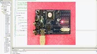
 MICROCHIP 5V CAN LIN Starter Kit for Digital Signal Controllers (DSCs) - PDF - Farnell Element 14
MICROCHIP 5V CAN LIN Starter Kit for Digital Signal Controllers (DSCs) - PDF - Farnell Element 14
- Revenir à l'accueil


Farnell Element 14 :


See the trailer for the next exciting episode of The Ben Heck show. Check back on Friday to be among the first to see the exclusive full show on element…

Connect your Raspberry Pi to a breadboard, download some code and create a push-button audio play project.


Puce électronique / Microchip :


Sans fil - Wireless :


Texas instrument :


Ordinateurs :


Logiciels :


Tutoriels :


Documents PDF :
![[TXT]](http://www.audentia-gestion.fr/icons/text.gif)
Farnell-ATMEL-8-bit-..> 10-Mar-2014 17:19 2.1M
Farnell-BYV79E-serie..> 10-Mar-2014 16:19 1.6M
Farnell-CIRRUS-LOGIC..> 10-Mar-2014 17:20 2.1M
Farnell-FICHE-DE-DON..> 10-Mar-2014 16:17 1.6M
Farnell-HUNTSMAN-Adv..> 10-Mar-2014 16:17 1.7M
Farnell-MOLEX-39-00-..> 10-Mar-2014 17:19 1.9M
Farnell-MOLEX-43020-..> 10-Mar-2014 17:21 1.9M
Farnell-MOLEX-43160-..> 10-Mar-2014 17:21 1.9M
Farnell-MOLEX-87439-..> 10-Mar-2014 17:21 1.9M
Farnell-Molex-Crimp-..> 10-Mar-2014 16:27 1.7M
Farnell-NXP-74VHC126..> 10-Mar-2014 16:17 1.6M
Farnell-NXP-PBSS9110..> 10-Mar-2014 17:21 1.9M
Farnell-NXP-PMBFJ620..> 10-Mar-2014 16:16 1.7M
Farnell-NXP-PSMN1R7-..> 10-Mar-2014 16:17 1.6M
Farnell-NXP-PSMN7R0-..> 10-Mar-2014 17:19 2.1M
Farnell-OMRON-Master..> 10-Mar-2014 16:26 1.8M
Farnell-Pico-Spox-Wi..> 10-Mar-2014 16:16 1.7M
Farnell-Proskit-SS-3..> 10-Mar-2014 16:26 1.8M
Farnell-TEKTRONIX-DP..> 10-Mar-2014 17:20 2.0M
Farnell-Tektronix-AC..> 10-Mar-2014 15:52 1.5M
Farnell-The-essentia..> 10-Mar-2014 16:27 1.7M
Farnell-manual-bus-p..> 10-Mar-2014 16:29 1.9M
Farnell-uC-OS-III-Br..> 10-Mar-2014 17:20 2.0M
![[TXT]](http://www.audentia-gestion.fr/__ovh_icons/text.gif) 0.20W-0402-2-TERM-0...> 29-Jul-2015 16:15 1.2M
0.20W-0402-2-TERM-0...> 29-Jul-2015 16:15 1.2M
![[DIR]](http://www.audentia-gestion.fr/__ovh_icons/folder.gif) ATmega/ 09-Jul-2015 11:27 -
Analog-Devices-ADC-S..> 09-Sep-2014 08:21 2.4M
Analog-Devices-ADMC2..> 09-Sep-2014 08:21 2.4M
Analog-Devices-ADMC4..> 09-Sep-2014 08:23 2.3M
Analog-Devices-AN300..> 08-Sep-2014 17:42 2.0M
Analog-Devices-ANF32..> 09-Sep-2014 08:18 2.6M
Analog-Devices-Basic..> 08-Sep-2014 17:49 1.9M
Analog-Devices-Compl..> 08-Sep-2014 17:38 2.0M
Analog-Devices-Convo..> 09-Sep-2014 08:26 2.1M
Analog-Devices-Convo..> 09-Sep-2014 08:25 2.2M
Analog-Devices-Convo..> 09-Sep-2014 08:25 2.2M
Analog-Devices-Digit..> 08-Sep-2014 18:02 2.1M
Analog-Devices-Digit..> 08-Sep-2014 18:03 2.0M
Analog-Devices-Gloss..> 08-Sep-2014 17:36 2.0M
Analog-Devices-Intro..> 08-Sep-2014 17:39 1.9M
Analog-Devices-The-C..> 08-Sep-2014 17:41 1.9M
Analog-Devices-Visua..> 09-Sep-2014 08:18 2.5M
Analog-Devices-Wi-Fi..> 09-Sep-2014 08:23 2.3M
Crucial-Ballistix-El..> 20-Dec-2014 16:42 8.0M
Crucial-Data-Transfe..> 20-Dec-2014 16:39 8.1M
Crucial-Guide-pour-l..> 20-Dec-2014 16:37 8.1M
Crucial-Guide-pratiq..> 20-Dec-2014 16:37 8.1M
Crucial-Guide-pratiq..> 20-Dec-2014 16:42 8.0M
Crucial-Technologie-..> 20-Dec-2014 16:45 8.0M
Crucial-The-power-de..> 20-Dec-2014 16:39 8.1M
Crucial-View-our-DDR..> 20-Dec-2014 16:45 8.0M
Electronique-Basic-o..> 08-Sep-2014 17:43 1.8M
Farnell-0050375063-D..> 18-Jul-2014 17:03 2.5M
Farnell-03-iec-runds..> 04-Jul-2014 10:40 3.7M
Farnell-0430300011-D..> 14-Jun-2014 18:13 2.0M
Farnell-0433751001-D..> 18-Jul-2014 17:02 2.5M
Farnell-06-6544-8-PD..> 26-Mar-2014 17:56 2.7M
Farnell-1N4148WS-Fai..> 06-Jul-2014 10:04 1.9M
Farnell-2-GBPS-Diffe..> 28-Jul-2014 17:42 2.7M
Farnell-2N3906-Fairc..> 08-Sep-2014 07:22 2.1M
Farnell-2N7002DW-Fai..> 06-Jul-2014 10:03 886K
Farnell-3M-Polyimide..> 21-Mar-2014 08:09 3.9M
Farnell-3M-VolitionT..> 25-Mar-2014 08:18 3.3M
Farnell-4-Bit-Magnit..> 08-Jul-2014 18:53 2.2M
Farnell-7-Amphenol-A..> 09-Jul-2015 11:13 2.4M
Farnell-8-bit-Atmel-..> 20-Dec-2014 11:01 2.0M
Farnell-8-bit-serial..> 03-Jun-2015 18:00 2.4M
Farnell-10BQ060-PDF.htm 14-Jun-2014 09:50 2.4M
Farnell-10TPB47M-End..> 14-Jun-2014 18:16 3.4M
Farnell-12mm-Size-In..> 14-Jun-2014 09:50 2.4M
Farnell-24AA024-24LC..> 23-Jun-2014 10:26 3.1M
Farnell-50A-High-Pow..> 20-Mar-2014 17:31 2.9M
Farnell-74AC00-74ACT..> 06-Jul-2014 10:03 911K
Farnell-74HC_HCT273-..> 09-Jul-2015 11:18 2.0M
Farnell-74LCX573-Fai..> 06-Jul-2014 10:05 1.9M
Farnell-197.31-KB-Te..> 04-Jul-2014 10:42 3.3M
Farnell-270-Series-O..> 08-Jul-2014 18:49 2.3M
Farnell-760G-French-..> 07-Jul-2014 19:45 1.2M
Farnell-851-Series-P..> 08-Jul-2014 18:47 3.0M
Farnell-900-Series-B..> 08-Jul-2014 18:50 2.3M
Farnell-1734-ARALDIT..> 07-Jul-2014 19:45 1.2M
Farnell-1907-2006-PD..> 26-Mar-2014 17:56 2.7M
Farnell-2020-Manuel-..> 08-Jul-2014 18:55 2.1M
Farnell-3367-ARALDIT..> 07-Jul-2014 19:46 1.2M
Farnell-5910-PDF.htm 25-Mar-2014 08:15 3.0M
Farnell-6517b-Electr..> 29-Mar-2014 11:12 3.3M
Farnell-43031-0002-M..> 18-Jul-2014 17:03 2.5M
Farnell-7491181012-O..> 20-Dec-2014 10:22 2.6M
Farnell-A-4-Hardener..> 07-Jul-2014 19:44 1.4M
Farnell-A-True-Syste..> 29-Mar-2014 11:13 3.3M
Farnell-AC-DC-Power-..> 15-Jul-2014 16:47 845K
Farnell-ACC-Silicone..> 04-Jul-2014 10:40 3.7M
Farnell-AD524-PDF.htm 20-Mar-2014 17:33 2.8M
Farnell-AD584-Rev-C-..> 08-Sep-2014 07:20 2.2M
Farnell-AD586BRZ-Ana..> 08-Sep-2014 08:09 1.6M
Farnell-AD620-Rev-H-..> 09-Sep-2014 08:13 2.6M
Farnell-AD736-Rev-I-..> 08-Sep-2014 07:31 1.3M
Farnell-AD7171-16-Bi..> 06-Jul-2014 10:06 1.0M
Farnell-AD7719-Low-V..> 18-Jul-2014 16:59 1.4M
Farnell-AD8300-Data-..> 18-Jul-2014 16:56 1.3M
Farnell-AD8307-Data-..> 08-Sep-2014 07:30 1.3M
Farnell-AD8310-Analo..> 08-Sep-2014 07:24 2.1M
Farnell-AD8313-Analo..> 08-Sep-2014 07:26 2.0M
Farnell-AD8361-Rev-D..> 08-Sep-2014 07:23 2.1M
Farnell-AD9833-Rev-E..> 08-Sep-2014 17:49 1.8M
Farnell-AD9834-Rev-D..> 08-Sep-2014 07:32 1.2M
Farnell-ADE7753-Rev-..> 08-Sep-2014 07:20 2.3M
Farnell-ADE7758-Rev-..> 08-Sep-2014 07:28 1.7M
Farnell-ADL6507-PDF.htm 14-Jun-2014 18:19 3.4M
Farnell-ADSP-21362-A..> 20-Mar-2014 17:34 2.8M
Farnell-ADuM1200-ADu..> 08-Sep-2014 08:09 1.6M
Farnell-ADuM1300-ADu..> 08-Sep-2014 08:11 1.7M
Farnell-ALF1210-PDF.htm 06-Jul-2014 10:06 4.0M
Farnell-ALF1225-12-V..> 01-Apr-2014 07:40 3.4M
Farnell-ALF2412-24-V..> 01-Apr-2014 07:39 3.4M
Farnell-AN2794-Appli..> 13-Oct-2014 07:01 1.0M
Farnell-AN10361-Phil..> 23-Jun-2014 10:29 2.1M
Farnell-ARADUR-HY-13..> 26-Mar-2014 17:55 2.8M
Farnell-ARALDITE-201..> 21-Mar-2014 08:12 3.7M
Farnell-ARALDITE-CW-..> 26-Mar-2014 17:56 2.7M
Farnell-AT42QT1010-D..> 20-Dec-2014 11:43 4.4M
Farnell-AT42QT1040-M..> 20-Dec-2014 11:44 4.4M
Farnell-AT89C5131-Ha..> 29-Jul-2014 10:31 1.2M
Farnell-AT90USB64-12..> 20-Dec-2014 10:59 4.4M
Farnell-AT90USBKey-H..> 29-Jul-2014 10:31 902K
Farnell-ATMEL-8-bit-..> 19-Mar-2014 18:04 2.1M
Farnell-ATMEL-8-bit-..> 11-Mar-2014 07:55 2.1M
Farnell-ATTINY4-5-9-..> 20-Dec-2014 11:42 2.0M
Farnell-ATmega8-L-da..> 20-Dec-2014 11:41 2.6M
Farnell-ATmega8A-dat..> 20-Dec-2014 11:41 3.1M
Farnell-ATmega48-88-..> 20-Dec-2014 10:59 3.6M
Farnell-ATmega48-88-..> 03-Jun-2015 18:09 3.2M
Farnell-ATmega329-32..> 20-Dec-2014 11:37 4.9M
Farnell-ATmega640-VA..> 14-Jun-2014 09:49 2.5M
Farnell-ATmega1284P-..> 09-Jul-2015 11:21 1.7M
Farnell-ATtiny20-PDF..> 25-Mar-2014 08:19 3.6M
Farnell-ATtiny24A-44..> 09-Jul-2015 11:19 2.0M
Farnell-ATtiny24A-44..> 20-Dec-2014 11:38 3.8M
Farnell-ATtiny25-V-A..> 20-Dec-2014 16:55 6.9M
Farnell-ATtiny26-L-A..> 18-Jul-2014 17:00 2.6M
Farnell-ATtiny26-L-A..> 13-Jun-2014 18:40 1.8M
Farnell-ATtiny1634-d..> 20-Dec-2014 11:44 5.5M
Farnell-ATtiny2313-A..> 20-Dec-2014 09:47 1.6M
Farnell-ATtiny2313A-..> 20-Dec-2014 11:37 4.3M
Farnell-ATxmega128A1..> 20-Dec-2014 11:39 3.4M
Farnell-AVR172-Senso..> 20-Dec-2014 09:47 1.2M
Farnell-Alimentation..> 07-Jul-2014 19:43 1.8M
Farnell-Alimentation..> 14-Jun-2014 18:24 2.5M
Farnell-Alimentation..> 01-Apr-2014 07:42 3.4M
Farnell-Amplificateu..> 29-Mar-2014 11:11 3.3M
Farnell-Amplifier-In..> 06-Jul-2014 10:02 940K
Farnell-An-Improved-..> 14-Jun-2014 09:49 2.5M
Farnell-Araldite-Fus..> 07-Jul-2014 19:45 1.2M
Farnell-Arithmetic-L..> 08-Jul-2014 18:54 2.1M
Farnell-Atmel-AT42QT..> 20-Dec-2014 16:57 5.5M
Farnell-Atmel-ATmega..> 19-Mar-2014 18:03 2.2M
Farnell-Atmel-ATtiny..> 20-Dec-2014 11:00 2.5M
Farnell-Atmel-AVR192..> 20-Dec-2014 11:41 2.6M
Farnell-Atmel-ICE-US..> 20-Dec-2014 11:00 2.1M
Farnell-Atmel-OLED1-..> 20-Dec-2014 16:59 5.5M
Farnell-Atmel-QTouch..> 20-Dec-2014 11:00 2.9M
Farnell-Atmel-SAM4S-..> 20-Dec-2014 11:39 3.2M
Farnell-Atmel-Xplain..> 20-Dec-2014 11:38 3.4M
Farnell-Avvertenze-e..> 14-Jun-2014 18:20 3.3M
Farnell-BA-Series-Oh..> 08-Jul-2014 18:50 2.3M
Farnell-BAT54J-Schot..> 20-Dec-2014 09:47 1.1M
Farnell-BAV99-Fairch..> 06-Jul-2014 10:03 896K
Farnell-BAV756S_BAW5..> 09-Jul-2015 11:18 2.0M
Farnell-BC846DS-NXP-..> 13-Jun-2014 18:42 1.6M
Farnell-BC846DS2-NXP..> 20-Dec-2014 09:48 1.2M
Farnell-BC847DS-NXP-..> 23-Jun-2014 10:24 3.3M
Farnell-BD6xxx-PDF.htm 22-Jul-2014 12:33 1.6M
Farnell-BF545A-BF545..> 23-Jun-2014 10:28 2.1M
Farnell-BGA7124-400-..> 18-Jul-2014 16:59 1.5M
Farnell-BK889B-PONT-..> 07-Jul-2014 19:42 1.8M
Farnell-BK2650A-BK26..> 29-Mar-2014 11:10 3.3M
Farnell-BT151-650R-N..> 13-Jun-2014 18:40 1.7M
Farnell-BTA204-800C-..> 13-Jun-2014 18:42 1.6M
Farnell-BUJD203AX-NX..> 13-Jun-2014 18:41 1.7M
Farnell-BYV29F-600-N..> 13-Jun-2014 18:42 1.6M
Farnell-BYV79E-serie..> 10-Mar-2014 16:19 1.6M
Farnell-BZX384-serie..> 23-Jun-2014 10:29 2.1M
Farnell-Battery-GBA-..> 14-Jun-2014 18:13 2.0M
Farnell-Both-the-Del..> 06-Jul-2014 10:01 948K
Farnell-C.A-6150-C.A..> 14-Jun-2014 18:24 2.5M
Farnell-C.A 8332B-C...> 01-Apr-2014 07:40 3.4M
Farnell-CC-Debugger-..> 07-Jul-2014 19:44 1.5M
Farnell-CC2530ZDK-Us..> 08-Jul-2014 18:55 2.1M
Farnell-CC2531-USB-H..> 07-Jul-2014 19:43 1.8M
Farnell-CC2560-Bluet..> 29-Mar-2014 11:14 2.8M
Farnell-CD4066B-Rev-..> 09-Jul-2015 11:20 1.8M
Farnell-CD4536B-Type..> 14-Jun-2014 18:13 2.0M
Farnell-CIRRUS-LOGIC..> 10-Mar-2014 17:20 2.1M
Farnell-CLASS 1-or-2..> 22-Jul-2014 12:30 4.7M
Farnell-CLRC632-NXP-..> 20-Dec-2014 10:22 2.6M
Farnell-CRC-HANDCLEA..> 07-Jul-2014 19:46 1.2M
Farnell-CS5532-34-BS..> 01-Apr-2014 07:39 3.5M
Farnell-Cannon-ZD-PD..> 11-Mar-2014 08:13 2.8M
Farnell-Ceramic-tran..> 14-Jun-2014 18:19 3.4M
Farnell-Circuit-Impr..> 25-Jul-2014 12:22 3.1M
Farnell-Circuit-Note..> 26-Mar-2014 18:00 2.8M
Farnell-Circuit-Note..> 26-Mar-2014 18:00 2.8M
Farnell-Cles-electro..> 21-Mar-2014 08:13 3.9M
Farnell-Clipper-Seri..> 08-Jul-2014 18:48 2.8M
Farnell-Compensating..> 09-Sep-2014 08:16 2.6M
Farnell-Compensating..> 09-Sep-2014 08:16 2.6M
Farnell-Conception-d..> 11-Mar-2014 07:49 2.4M
Farnell-Connectors-N..> 14-Jun-2014 18:12 2.1M
Farnell-Construction..> 14-Jun-2014 18:25 2.5M
Farnell-Controle-de-..> 11-Mar-2014 08:16 2.8M
Farnell-Cordless-dri..> 14-Jun-2014 18:13 2.0M
Farnell-Crucial-Ball..> 20-Dec-2014 16:48 8.0M
Farnell-Crucial-DDR4..> 20-Dec-2014 16:53 7.6M
Farnell-Cube-3D-Prin..> 18-Jul-2014 17:02 2.5M
Farnell-Current-Tran..> 26-Mar-2014 17:58 2.7M
Farnell-Current-Tran..> 26-Mar-2014 17:58 2.7M
Farnell-Current-Tran..> 26-Mar-2014 17:59 2.7M
Farnell-Current-Tran..> 26-Mar-2014 17:59 2.7M
Farnell-DAC8143-Data..> 18-Jul-2014 16:59 1.5M
Farnell-DC-DC-Conver..> 15-Jul-2014 16:48 781K
Farnell-DC-Fan-type-..> 14-Jun-2014 09:48 2.5M
Farnell-DC-Fan-type-..> 14-Jun-2014 09:51 1.8M
Farnell-DG411-DG412-..> 07-Jul-2014 19:47 1.0M
Farnell-DP83846A-DsP..> 18-Jul-2014 16:55 1.5M
Farnell-DS3231-DS-PD..> 18-Jul-2014 16:57 2.5M
Farnell-Data-Sheet-J..> 20-Dec-2014 10:21 1.0M
Farnell-Data-Sheet-J..> 20-Dec-2014 10:20 1.2M
Farnell-Data-Sheet-K..> 07-Jul-2014 19:46 1.2M
Farnell-Data-Sheet-M..> 09-Jul-2015 11:18 2.1M
Farnell-Data-Sheet-M..> 09-Jul-2015 11:17 2.1M
Farnell-Data-Sheet-M..> 09-Sep-2014 08:05 2.8M
Farnell-Data-Sheet-S..> 18-Jul-2014 17:00 1.2M
Farnell-Datasheet-FT..> 09-Sep-2014 08:10 2.8M
Farnell-Datasheet-Fa..> 06-Jul-2014 10:04 861K
Farnell-Datasheet-Fa..> 15-Jul-2014 17:05 1.0M
Farnell-Datasheet-NX..> 03-Jun-2015 18:10 2.5M
Farnell-Datasheet-NX..> 20-Dec-2014 09:52 1.6M
Farnell-Davum-TMC-PD..> 14-Jun-2014 18:27 2.4M
Farnell-De-la-puissa..> 29-Mar-2014 11:10 3.3M
Farnell-Decapant-KF-..> 07-Jul-2014 19:45 1.2M
Farnell-Directive-re..> 25-Mar-2014 08:16 3.0M
Farnell-Documentatio..> 14-Jun-2014 18:26 2.5M
Farnell-Download-dat..> 16-Jul-2014 09:02 2.2M
Farnell-Download-dat..> 13-Jun-2014 18:40 1.8M
Farnell-Drawing-Octo..> 09-Jul-2015 11:13 2.4M
Farnell-Dremel-Exper..> 22-Jul-2014 12:34 1.6M
Farnell-Dual-MOSFET-..> 28-Jul-2014 17:41 2.8M
Farnell-ECO-Series-T..> 20-Mar-2014 08:14 2.5M
Farnell-EE-SPX303N-4..> 15-Jul-2014 17:06 969K
Farnell-ELMA-PDF.htm 29-Mar-2014 11:13 3.3M
Farnell-EMC1182-PDF.htm 25-Mar-2014 08:17 3.0M
Farnell-EPCOS-173438..> 04-Jul-2014 10:43 3.3M
Farnell-EPCOS-Sample..> 11-Mar-2014 07:53 2.2M
Farnell-ES1F-ES1J-fi..> 06-Jul-2014 10:04 867K
Farnell-ES2333-PDF.htm 11-Mar-2014 08:14 2.8M
Farnell-ESCON-Featur..> 06-Jul-2014 10:05 938K
Farnell-ESCON-Featur..> 06-Jul-2014 10:02 931K
Farnell-ESM6045DV-ST..> 13-Oct-2014 07:06 850K
Farnell-ESMT-M52D323..> 20-Dec-2014 16:50 7.6M
Farnell-Ed.081002-DA..> 19-Mar-2014 18:02 2.5M
Farnell-Encodeur-USB..> 08-Jul-2014 18:56 2.0M
Farnell-Evaluating-t..> 22-Jul-2014 12:28 4.9M
Farnell-Everything-Y..> 11-Oct-2014 12:05 1.5M
Farnell-Excalibur-Hi..> 28-Jul-2014 17:10 2.4M
Farnell-Excalibur-Hi..> 28-Jul-2014 17:10 2.4M
Farnell-Explorer-16-..> 29-Jul-2014 10:31 1.3M
Farnell-F28069-Picco..> 14-Jun-2014 18:14 2.0M
Farnell-F42202-PDF.htm 19-Mar-2014 18:00 2.5M
Farnell-FAN6756-Fair..> 06-Jul-2014 10:04 850K
Farnell-FDC2512-Fair..> 06-Jul-2014 10:03 886K
Farnell-FDS-ITW-Spra..> 14-Jun-2014 18:22 3.3M
Farnell-FDV301N-Digi..> 06-Jul-2014 10:03 886K
Farnell-FICHE-DE-DON..> 10-Mar-2014 16:17 1.6M
Farnell-FSDM0565RB-F..> 09-Jul-2015 11:23 1.2M
Farnell-Fairchild-2N..> 09-Jul-2015 11:20 1.8M
Farnell-Fairchild-FD..> 09-Jul-2015 11:21 1.7M
Farnell-Fast-Charge-..> 28-Jul-2014 17:12 6.4M
Farnell-Fastrack-Sup..> 23-Jun-2014 10:25 3.3M
Farnell-Ferric-Chlor..> 29-Mar-2014 11:14 2.8M
Farnell-Fiche-de-don..> 14-Jun-2014 09:47 2.5M
Farnell-Fiche-de-don..> 14-Jun-2014 18:26 2.5M
Farnell-Fluke-1730-E..> 14-Jun-2014 18:23 2.5M
Farnell-Fluke-Ti400-..> 20-Dec-2014 16:48 8.0M
Farnell-Full-Datashe..> 15-Jul-2014 17:08 951K
Farnell-Full-Datashe..> 15-Jul-2014 16:47 803K
Farnell-GALVA-A-FROI..> 26-Mar-2014 17:56 2.7M
Farnell-GALVA-MAT-Re..> 26-Mar-2014 17:57 2.7M
Farnell-GN-RELAYS-AG..> 20-Mar-2014 08:11 2.6M
Farnell-Gertboard-Us..> 29-Jul-2014 10:30 1.4M
Farnell-HC49-4H-Crys..> 14-Jun-2014 18:20 3.3M
Farnell-HEF4052B-NXP..> 09-Jul-2015 11:18 2.0M
Farnell-HFE1600-Data..> 14-Jun-2014 18:22 3.3M
Farnell-HI-70300-Sol..> 14-Jun-2014 18:27 2.4M
Farnell-HIP4081A-Int..> 07-Jul-2014 19:47 1.0M
Farnell-HUNTSMAN-Adv..> 10-Mar-2014 16:17 1.7M
Farnell-Haute-vitess..> 20-Dec-2014 18:50 2.4M
Farnell-Hex-Inverter..> 29-Jul-2014 10:31 875K
Farnell-High-precisi..> 08-Jul-2014 18:51 2.3M
Farnell-ICM7228-Inte..> 07-Jul-2014 19:46 1.1M
Farnell-IP4251_52_53..> 20-Dec-2014 09:51 1.6M
Farnell-IP4252CZ16-8..> 13-Jun-2014 18:41 1.7M
Farnell-ISL6251-ISL6..> 07-Jul-2014 19:47 1.1M
Farnell-Instructions..> 19-Mar-2014 18:01 2.5M
Farnell-Jeu-multi-la..> 25-Jul-2014 12:23 3.0M
Farnell-KA3525A-SMPS..> 09-Jul-2015 11:23 1.2M
Farnell-KSZ8851SNL-S..> 23-Jun-2014 10:28 2.1M
Farnell-Keyboard-Mou..> 22-Jul-2014 12:27 5.9M
Farnell-L-efficacite..> 11-Mar-2014 07:52 2.3M
Farnell-L78-Positive..> 13-Oct-2014 07:04 1.8M
Farnell-L78-STMicroe..> 11-Oct-2014 15:49 1.6M
Farnell-L78S-STMicro..> 22-Jul-2014 12:32 1.6M
Farnell-L293B-STMicr..> 11-Oct-2014 15:49 1.7M
Farnell-L293d-Texas-..> 08-Jul-2014 18:53 2.2M
Farnell-L4978-STMicr..> 13-Oct-2014 07:07 783K
Farnell-L6384E-STMic..> 13-Oct-2014 07:02 1.9M
Farnell-L6562-STMicr..> 13-Oct-2014 07:07 754K
Farnell-LCW-CQ7P.CC-..> 25-Mar-2014 08:19 3.2M
Farnell-LD-WSECO16-P..> 25-Jul-2014 12:22 3.1M
Farnell-LF351-STMicr..> 11-Oct-2014 15:49 1.7M
Farnell-LM3S6952-Mic..> 22-Jul-2014 12:27 5.9M
Farnell-LM19-Texas-I..> 18-Jul-2014 17:00 1.2M
Farnell-LM139-LM239-..> 13-Oct-2014 07:07 771K
Farnell-LM158-LM258-..> 11-Oct-2014 15:49 1.6M
Farnell-LM217-LM317-..> 13-Oct-2014 07:04 1.7M
Farnell-LM324-Texas-..> 29-Jul-2014 10:32 1.5M
Farnell-LM350-STMicr..> 13-Oct-2014 07:03 1.8M
Farnell-LM386-Low-Vo..> 29-Jul-2014 10:32 1.5M
Farnell-LM555-Timer-..> 08-Jul-2014 18:53 2.2M
Farnell-LM2904-LM290..> 13-Oct-2014 07:04 1.7M
Farnell-LM7805-Fairc..> 09-Sep-2014 08:13 2.7M
Farnell-LME49725-Pow..> 14-Jun-2014 09:49 2.5M
Farnell-LMH6518-Texa..> 18-Jul-2014 16:59 1.3M
Farnell-LMP91051-Use..> 29-Jul-2014 10:30 1.4M
Farnell-LMT88-2.4V-1..> 28-Jul-2014 17:42 2.8M
Farnell-LOCTITE-542-..> 25-Mar-2014 08:15 3.0M
Farnell-LOCTITE-3463..> 25-Mar-2014 08:19 3.0M
Farnell-LPC11U3x-32-..> 16-Jul-2014 09:01 2.4M
Farnell-LPC81xM-32-b..> 16-Jul-2014 09:02 2.0M
Farnell-LPC81xM-NXP-..> 20-Dec-2014 10:26 1.2M
Farnell-LPC178x-7x-N..> 20-Dec-2014 10:21 1.6M
Farnell-LPC408x-7x 3..> 16-Jul-2014 09:03 1.6M
Farnell-LPC1769-68-6..> 16-Jul-2014 09:02 1.9M
Farnell-LPC1769-68-6..> 20-Dec-2014 10:06 2.2M
Farnell-LPC2141-42-4..> 09-Jul-2015 11:23 1.5M
Farnell-LPC2364-65-6..> 09-Jul-2015 11:23 1.4M
Farnell-LPC2468-NXP-..> 09-Jul-2015 11:23 1.6M
Farnell-LPC3220-30-4..> 16-Jul-2014 09:02 2.2M
Farnell-LPC4350-30-2..> 20-Dec-2014 10:21 1.4M
Farnell-LQ-RELAYS-AL..> 06-Jul-2014 10:02 924K
Farnell-LT1961-Linea..> 18-Jul-2014 16:58 1.6M
Farnell-LT3757-Linea..> 18-Jul-2014 16:58 1.6M
Farnell-LT6233-Linea..> 18-Jul-2014 16:56 1.3M
Farnell-LUMINARY-MIC..> 22-Jul-2014 12:31 3.6M
Farnell-LUXEON-Guide..> 11-Mar-2014 07:52 2.3M
Farnell-Leaded-Trans..> 23-Jun-2014 10:26 3.2M
Farnell-Les-derniers..> 11-Mar-2014 07:50 2.3M
Farnell-Loctite3455-..> 25-Mar-2014 08:16 3.0M
Farnell-Low-Noise-24..> 06-Jul-2014 10:05 1.0M
Farnell-Low-cost-Enc..> 13-Jun-2014 18:42 1.7M
Farnell-Lubrifiant-a..> 26-Mar-2014 18:00 2.7M
Farnell-M68000-PDF.htm 09-Jul-2015 11:22 1.7M
Farnell-MAX200-MAX20..> 09-Jul-2015 11:16 2.2M
Farnell-MAX202E-MAX2..> 09-Jul-2015 11:15 2.2M
Farnell-MAX232-MAX23..> 08-Jul-2014 18:52 2.3M
Farnell-MAX481-MAX48..> 09-Jul-2015 11:16 2.1M
Farnell-MAX756-MAX75..> 09-Jul-2015 11:16 2.2M
Farnell-MAX1365-MAX1..> 18-Jul-2014 16:56 1.4M
Farnell-MAX3221-Rev-..> 08-Sep-2014 07:28 1.8M
Farnell-MAX3222-MAX3..> 09-Jul-2015 11:16 2.1M
Farnell-MAX4661-MAX4..> 09-Sep-2014 08:10 2.8M
Farnell-MB85RS128B-F..> 20-Dec-2014 09:38 1.1M
Farnell-MC3510-PDF.htm 25-Mar-2014 08:17 3.0M
Farnell-MC21605-PDF.htm 15-Jan-2016 11:02 2.8M
Farnell-MC34063ABD-T..> 13-Oct-2014 07:06 844K
Farnell-MCF532x-7x-E..> 29-Mar-2014 11:14 2.8M
Farnell-MCOC1-Farnel..> 16-Jul-2014 09:04 1.0M
Farnell-MCP3421-Micr..> 18-Jul-2014 17:00 1.2M
Farnell-MIC809-MIC81..> 09-Jul-2015 11:13 2.4M
Farnell-MICREL-KSZ88..> 11-Mar-2014 07:54 2.2M
Farnell-MICROCHIP-PI..> 19-Mar-2014 18:02 2.5M
Farnell-MICROCHIP-PI..> 25-Jul-2014 12:34 6.7M
Farnell-MIDAS-un-tra..> 15-Jul-2014 17:05 1.0M
Farnell-MMBZxVCL-MMB..> 20-Dec-2014 09:53 1.6M
Farnell-MOLEX-39-00-..> 10-Mar-2014 17:19 1.9M
Farnell-MOLEX-43020-..> 10-Mar-2014 17:21 1.9M
Farnell-MOLEX-43160-..> 10-Mar-2014 17:21 1.9M
Farnell-MOLEX-87439-..> 10-Mar-2014 17:21 1.9M
Farnell-MPXV7002-Rev..> 20-Mar-2014 17:33 2.8M
Farnell-MSP-EXP430F5..> 29-Jul-2014 10:31 1.2M
Farnell-MSP430-Hardw..> 29-Jul-2014 10:36 1.1M
Farnell-MSP430F15x-M..> 08-Sep-2014 07:32 1.3M
Farnell-MTX-3250-MTX..> 18-Jul-2014 17:01 2.5M
Farnell-MTX-Compact-..> 18-Jul-2014 17:01 2.5M
Farnell-MULTICOMP-Ra..> 22-Jul-2014 12:57 5.9M
Farnell-MX670-MX675-..> 14-Jun-2014 09:46 2.5M
Farnell-Maxim-MAX322..> 09-Jul-2015 11:17 2.1M
Farnell-Microchip-MC..> 13-Jun-2014 18:27 1.8M
Farnell-Microship-PI..> 11-Mar-2014 07:53 2.2M
Farnell-Midas-Active..> 14-Jun-2014 18:17 3.4M
Farnell-Midas-MCCOG4..> 14-Jun-2014 18:11 2.1M
Farnell-Mini-Fit-Jr-..> 18-Jul-2014 17:03 2.5M
Farnell-Miniature-Ci..> 26-Mar-2014 17:55 2.8M
Farnell-Mistral-PDF.htm 14-Jun-2014 18:12 2.1M
Farnell-Molex-83421-..> 14-Jun-2014 18:17 3.4M
Farnell-Molex-COMMER..> 14-Jun-2014 18:16 3.4M
Farnell-Molex-Crimp-..> 10-Mar-2014 16:27 1.7M
Farnell-Multi-Functi..> 20-Mar-2014 17:38 3.0M
Farnell-NA555-NE555-..> 08-Jul-2014 18:53 2.2M
Farnell-NA555-NE555-..> 08-Sep-2014 07:51 1.5M
Farnell-NE556-SA556-..> 11-Oct-2014 15:48 1.7M
Farnell-NE5532-Texas..> 29-Jul-2014 10:32 1.5M
Farnell-NT3H1101-NT3..> 20-Dec-2014 10:06 2.3M
Farnell-NTE_SEMICOND..> 11-Mar-2014 07:52 2.3M
Farnell-NVE-datashee..> 28-Jul-2014 17:12 6.5M
Farnell-NXP-74VHC126..> 10-Mar-2014 16:17 1.6M
Farnell-NXP-BT136-60..> 11-Mar-2014 07:52 2.3M
Farnell-NXP-PBSS9110..> 10-Mar-2014 17:21 1.9M
Farnell-NXP-PCA9555 ..> 11-Mar-2014 07:54 2.2M
Farnell-NXP-PMBFJ620..> 10-Mar-2014 16:16 1.7M
Farnell-NXP-PSMN1R7-..> 10-Mar-2014 16:17 1.6M
Farnell-NXP-PSMN7R0-..> 10-Mar-2014 17:19 2.1M
Farnell-NXP-TEA1703T..> 11-Mar-2014 08:15 2.8M
Farnell-NaPiOn-Panas..> 06-Jul-2014 10:02 911K
Farnell-Nilï¬-sk-E-..> 14-Jun-2014 09:47 2.5M
Farnell-Novembre-201..> 20-Mar-2014 17:38 3.3M
Farnell-OMRON-INDUST..> 25-Jul-2014 12:31 6.9M
Farnell-OMRON-INDUST..> 25-Jul-2014 12:32 6.9M
Farnell-OMRON-Master..> 10-Mar-2014 16:26 1.8M
Farnell-OPA627-Texas..> 09-Sep-2014 08:08 2.8M
Farnell-OSLON-SSL-Ce..> 19-Mar-2014 18:03 2.1M
Farnell-OXPCIE958-FB..> 13-Jun-2014 18:40 1.8M
Farnell-Octal-D-type..> 03-Jun-2015 18:10 2.5M
Farnell-Octal-Genera..> 28-Jul-2014 17:42 2.8M
Farnell-PADO-semi-au..> 04-Jul-2014 10:41 3.7M
Farnell-PBSS5160T-60..> 19-Mar-2014 18:03 2.1M
Farnell-PBSS5320X-NX..> 20-Dec-2014 09:47 1.6M
Farnell-PCF8574-PCF8..> 16-Jul-2014 09:03 1.7M
Farnell-PDTA143X-ser..> 20-Mar-2014 08:12 2.6M
Farnell-PDTB123TT-NX..> 20-Dec-2014 09:39 1.0M
Farnell-PESD5V0F1BL-..> 20-Dec-2014 09:39 1.1M
Farnell-PESD5V0F1BL-..> 13-Jun-2014 18:43 1.5M
Farnell-PESD9X5.0L-P..> 13-Jun-2014 18:43 1.6M
Farnell-PIC12F529T39..> 20-Dec-2014 09:39 1.0M
Farnell-PIC12F609-61..> 04-Jul-2014 10:41 3.7M
Farnell-PIC18F1220-1..> 20-Dec-2014 16:53 7.5M
Farnell-PIC18F2420-2..> 20-Dec-2014 16:55 6.9M
Farnell-PIC18F2420-2..> 18-Jul-2014 16:57 2.5M
Farnell-PIC18F2455-2..> 23-Jun-2014 10:27 3.1M
Farnell-PIC18FXX2-Da..> 20-Dec-2014 16:58 6.2M
Farnell-PIC24FJ256GB..> 14-Jun-2014 09:51 2.4M
Farnell-PMBT3906-PNP..> 20-Dec-2014 09:39 1.0M
Farnell-PMBT3906-PNP..> 13-Jun-2014 18:44 1.5M
Farnell-PMBT4403-PNP..> 23-Jun-2014 10:27 3.1M
Farnell-PMEG3010EP-N..> 20-Dec-2014 09:47 1.1M
Farnell-PMEG4002EL-N..> 14-Jun-2014 18:18 3.4M
Farnell-PMEG4010CEH-..> 13-Jun-2014 18:43 1.6M
Farnell-PN512-Full-N..> 16-Jul-2014 09:03 1.4M
Farnell-PN512-NXP-Se..> 20-Dec-2014 10:01 1.9M
Farnell-PSMN011-80YS..> 20-Dec-2014 09:39 1.1M
Farnell-Panasonic-15..> 23-Jun-2014 10:29 2.1M
Farnell-Panasonic-Al..> 09-Jul-2015 11:22 1.7M
Farnell-Panasonic-EC..> 20-Mar-2014 17:36 2.6M
Farnell-Panasonic-EZ..> 20-Mar-2014 08:10 2.6M
Farnell-Panasonic-Id..> 20-Mar-2014 17:35 2.6M
Farnell-Panasonic-Ne..> 20-Mar-2014 17:36 2.6M
Farnell-Panasonic-Ra..> 20-Mar-2014 17:37 2.6M
Farnell-Panasonic-Ra..> 09-Jul-2015 11:22 1.6M
Farnell-Panasonic-TS..> 20-Mar-2014 08:12 2.6M
Farnell-Panasonic-Ty..> 09-Jul-2015 11:22 1.7M
Farnell-Panasonic-Y3..> 20-Mar-2014 08:11 2.6M
Farnell-PiFace-Digit..> 25-Jul-2014 12:25 3.0M
Farnell-Pico-Spox-Wi..> 10-Mar-2014 16:16 1.7M
Farnell-PicoScope-42..> 25-Jul-2014 12:23 3.0M
Farnell-PicoScope-se..> 25-Jul-2014 12:24 3.0M
Farnell-Pompes-Charg..> 24-Apr-2014 20:23 3.3M
Farnell-Ponts-RLC-po..> 14-Jun-2014 18:23 3.3M
Farnell-Portable-Ana..> 20-Dec-2014 18:49 2.8M
Farnell-Power-suppli..> 25-Jul-2014 12:29 7.0M
Farnell-Premier-Farn..> 21-Mar-2014 08:11 3.8M
Farnell-Processor-Su..> 09-Jul-2015 11:13 2.4M
Farnell-Produit-3430..> 14-Jun-2014 09:48 2.5M
Farnell-Proskit-SS-3..> 10-Mar-2014 16:26 1.8M
Farnell-Puissance-ut..> 11-Mar-2014 07:49 2.4M
Farnell-Q48-PDF.htm 23-Jun-2014 10:29 2.1M
Farnell-QRE1113-Fair..> 06-Jul-2014 10:03 879K
Farnell-QRE1113-QRE1..> 09-Jul-2015 11:14 2.4M
Farnell-Quadruple-2-..> 08-Sep-2014 07:29 1.5M
Farnell-Quick-Start-..> 25-Jul-2014 12:25 3.0M
Farnell-RASPBERRY-PI..> 22-Jul-2014 12:35 5.9M
Farnell-RDS-80-PDF.htm 18-Jul-2014 16:57 1.3M
Farnell-REF19x-Serie..> 20-Dec-2014 18:49 2.8M
Farnell-REF102-10V-P..> 28-Jul-2014 17:09 2.4M
Farnell-RF-short-tra..> 28-Jul-2014 17:16 6.3M
Farnell-Radial-Lead-..> 20-Mar-2014 08:12 2.6M
Farnell-RaspiCam-Doc..> 22-Jul-2014 12:32 1.6M
Farnell-Realiser-un-..> 11-Mar-2014 07:51 2.3M
Farnell-Reglement-RE..> 21-Mar-2014 08:08 3.9M
Farnell-Repartiteurs..> 14-Jun-2014 18:26 2.5M
Farnell-S-TRI-SWT860..> 21-Mar-2014 08:11 3.8M
Farnell-S1A-Fairchil..> 06-Jul-2014 10:03 896K
Farnell-SB175-Connec..> 11-Mar-2014 08:14 2.8M
Farnell-SB520-SB5100..> 22-Jul-2014 12:32 1.6M
Farnell-SEEDDIM138-F..> 09-Jul-2015 11:14 2.4M
Farnell-SERIAL-TFT-M..> 15-Jul-2014 17:05 1.0M
Farnell-SG2525A-SG35..> 20-Dec-2014 09:39 1.0M
Farnell-SICK-OPTIC-E..> 18-Jul-2014 16:58 1.5M
Farnell-SL3ICS1002-1..> 16-Jul-2014 09:05 2.5M
Farnell-SL3S1003_101..> 20-Dec-2014 10:06 2.0M
Farnell-SL3S1203_121..> 20-Dec-2014 10:01 2.0M
Farnell-SL3S1203_121..> 16-Jul-2014 09:04 1.1M
Farnell-SL3S4011_402..> 16-Jul-2014 09:03 1.1M
Farnell-SL59830-Inte..> 06-Jul-2014 10:11 1.0M
Farnell-SMAJ-STMicro..> 13-Oct-2014 07:07 734K
Farnell-SMBJ-Transil..> 29-Mar-2014 11:12 3.3M
Farnell-SMU-Instrume..> 08-Jul-2014 18:51 2.3M
Farnell-SN54HC164-SN..> 08-Sep-2014 07:25 2.0M
Farnell-SN54HC244-SN..> 08-Jul-2014 18:52 2.3M
Farnell-SN54LV4053A-..> 28-Jul-2014 17:20 5.9M
Farnell-SO967460-PDF..> 11-Oct-2014 12:05 2.9M
Farnell-SOT-23-Multi..> 11-Mar-2014 07:51 2.3M
Farnell-SOURIAU-Cont..> 08-Jul-2014 19:04 3.0M
Farnell-SPLC780A1-16..> 14-Jun-2014 18:25 2.5M
Farnell-SSC7102-Micr..> 23-Jun-2014 10:25 3.2M
Farnell-ST1S10PHR-ST..> 13-Oct-2014 07:06 820K
Farnell-ST3232B-ST32..> 13-Oct-2014 07:06 867K
Farnell-STEVAL-TDR02..> 13-Oct-2014 07:01 960K
Farnell-STK600-Expan..> 20-Dec-2014 11:41 3.2M
Farnell-STM32F030x4-..> 13-Oct-2014 07:06 1.1M
Farnell-STM32F103x8-..> 22-Jul-2014 12:33 1.6M
Farnell-STM32F103x8-..> 13-Oct-2014 07:06 1.0M
Farnell-STM32F205xx-..> 13-Oct-2014 07:05 1.7M
Farnell-STM32F405xx-..> 13-Oct-2014 07:05 1.4M
Farnell-STM32F405xxS..> 27-Aug-2014 18:27 1.8M
Farnell-STP16NF06L-n..> 13-Oct-2014 07:05 1.7M
Farnell-STP80NF55L-0..> 13-Oct-2014 07:05 1.7M
Farnell-SVPE-series-..> 14-Jun-2014 18:15 2.0M
Farnell-Schroff-A108..> 25-Jul-2014 12:27 2.8M
Farnell-Schroff-Main..> 25-Jul-2014 12:26 2.9M
Farnell-Schroff-mult..> 25-Jul-2014 12:26 2.9M
Farnell-Sensorless-C..> 04-Jul-2014 10:42 3.3M
Farnell-Septembre-20..> 20-Mar-2014 17:46 3.7M
Farnell-Serial-File-..> 06-Jul-2014 10:02 941K
Farnell-Serie-PicoSc..> 19-Mar-2014 18:01 2.5M
Farnell-Serie-Standa..> 14-Jun-2014 18:23 3.3M
Farnell-Series-2600B..> 20-Mar-2014 17:30 3.0M
Farnell-Series-TDS10..> 04-Jul-2014 10:39 4.0M
Farnell-Signal-PCB-R..> 14-Jun-2014 18:11 2.1M
Farnell-Silica-Gel-M..> 07-Jul-2014 19:46 1.2M
Farnell-Single-Chip-..> 08-Sep-2014 07:30 1.5M
Farnell-Smart-street..> 13-Oct-2014 07:02 1.8M
Farnell-SmartRF06-Ev..> 07-Jul-2014 19:43 1.6M
Farnell-Strangkuhlko..> 21-Mar-2014 08:09 3.9M
Farnell-Supercapacit..> 26-Mar-2014 17:57 2.7M
Farnell-Surge-arrest..> 20-Dec-2014 18:34 8.1M
Farnell-Synchronous-..> 08-Jul-2014 18:54 2.1M
Farnell-T672-3000-Se..> 08-Jul-2014 18:59 2.0M
Farnell-TAS1020B-USB..> 28-Jul-2014 17:19 6.2M
Farnell-TAS5707-Texa..> 09-Jul-2015 11:20 1.8M
Farnell-TCL-DC-traco..> 15-Jul-2014 16:46 858K
Farnell-TDA7296-STMi..> 11-Oct-2014 15:54 1.7M
Farnell-TDK-Lambda-H..> 14-Jun-2014 18:21 3.3M
Farnell-TEKTRONIX-DP..> 10-Mar-2014 17:20 2.0M
Farnell-TEL-5-Series..> 15-Jul-2014 16:47 814K
Farnell-TEN-8-WI-Ser..> 15-Jul-2014 16:46 939K
Farnell-TEP-150WI-Se..> 15-Jul-2014 16:47 837K
Farnell-TEXAS-INSTRU..> 22-Jul-2014 12:29 4.8M
Farnell-TEXAS-INSTRU..> 22-Jul-2014 12:31 2.4M
Farnell-TEXAS-INSTRU..> 22-Jul-2014 12:30 4.6M
Farnell-TIP41C-TIP42..> 13-Oct-2014 07:06 829K
Farnell-TIP102-TIP10..> 13-Oct-2014 07:06 853K
Farnell-TIS-Instruct..> 15-Jul-2014 16:47 845K
Farnell-TIS-series-t..> 15-Jul-2014 16:46 875K
Farnell-TKC2-Dusters..> 07-Jul-2014 19:46 1.2M
Farnell-TL082-Wide-B..> 28-Jul-2014 17:16 6.3M
Farnell-TL084-TL084A..> 11-Oct-2014 15:54 1.7M
Farnell-TLC5940-Texa..> 09-Jul-2015 11:19 2.0M
Farnell-TLV320AIC23B..> 08-Sep-2014 07:18 2.4M
Farnell-TLV320AIC325..> 28-Jul-2014 17:45 2.9M
Farnell-TMLM-Series-..> 15-Jul-2014 16:47 810K
Farnell-TMP006EVM-Us..> 29-Jul-2014 10:30 1.3M
Farnell-TMR-2-Series..> 15-Jul-2014 16:46 897K
Farnell-TMR-2-series..> 15-Jul-2014 16:48 787K
Farnell-TMR-3-WI-Ser..> 15-Jul-2014 16:46 939K
Farnell-TMS320F28055..> 28-Jul-2014 17:09 2.7M
Farnell-TOS-tracopow..> 15-Jul-2014 16:47 852K
Farnell-TPA31xxD2-Te..> 09-Jul-2015 11:20 1.9M
Farnell-TPS40060-Wid..> 28-Jul-2014 17:19 6.3M
Farnell-TSV6390-TSV6..> 28-Jul-2014 17:14 6.4M
Farnell-TXL-series-t..> 15-Jul-2014 16:47 829K
Farnell-TYCO-ELECTRO..> 25-Jul-2014 12:30 6.9M
Farnell-Tektronix-AC..> 13-Jun-2014 18:44 1.5M
Farnell-Telemetres-l..> 20-Mar-2014 17:46 3.7M
Farnell-Termometros-..> 14-Jun-2014 18:14 2.0M
Farnell-The-Discrete..> 08-Sep-2014 17:44 1.8M
Farnell-The-essentia..> 10-Mar-2014 16:27 1.7M
Farnell-Thermometre-..> 29-Jul-2014 10:30 1.4M
Farnell-Tiva-C-Serie..> 08-Jul-2014 18:49 2.6M
Farnell-Trust-Digita..> 25-Jul-2014 12:24 3.0M
Farnell-U2270B-PDF.htm 14-Jun-2014 18:15 3.4M
Farnell-ULINKpro-Deb..> 25-Jul-2014 12:35 5.9M
Farnell-ULN2001-ULN2..> 13-Oct-2014 07:02 1.9M
Farnell-ULN2003a-Tex..> 03-Jun-2015 18:10 2.5M
Farnell-ULN2803A-Rev..> 09-Sep-2014 19:26 2.9M
Farnell-ULQ2001-ULQ2..> 13-Oct-2014 07:02 1.9M
Farnell-USB-Buccanee..> 14-Jun-2014 09:48 2.5M
Farnell-USB-to-Seria..> 08-Sep-2014 07:27 2.0M
Farnell-USB1T11A-PDF..> 19-Mar-2014 18:03 2.1M
Farnell-UTO-Souriau-..> 08-Jul-2014 18:48 2.8M
Farnell-UTS-Series-S..> 08-Jul-2014 18:49 2.8M
Farnell-UTS-Series-S..> 08-Jul-2014 18:49 2.5M
Farnell-User-Guide-M..> 07-Jul-2014 19:41 2.0M
Farnell-V4N-PDF.htm 14-Jun-2014 18:11 2.1M
Farnell-VND920P-E-ST..> 13-Oct-2014 07:04 1.8M
Farnell-Videk-PDF.htm 06-Jul-2014 10:01 948K
Farnell-WIRE-WRAP-50..> 25-Jul-2014 12:34 5.9M
Farnell-WetTantalum-..> 11-Mar-2014 08:14 2.8M
Farnell-XPS-AC-Octop..> 14-Jun-2014 18:11 2.1M
Farnell-XPS-MC16-XPS..> 11-Mar-2014 08:15 2.8M
Farnell-XPSAF5130-PD..> 18-Jul-2014 16:56 1.4M
Farnell-YAGEO-DATA-S..> 11-Mar-2014 08:13 2.8M
Farnell-ZigBee-ou-le..> 11-Mar-2014 07:50 2.4M
Farnell-]74HC125-74H..> 03-Jun-2015 18:09 2.6M
Farnell-celpac-SUL84..> 21-Mar-2014 08:11 3.8M
Farnell-china_rohs_o..> 21-Mar-2014 10:04 3.9M
Farnell-cree-Xlamp-X..> 20-Mar-2014 17:34 2.8M
Farnell-cree-Xlamp-X..> 20-Mar-2014 17:35 2.7M
Farnell-cree-Xlamp-X..> 20-Mar-2014 17:31 2.9M
Farnell-cree-Xlamp-m..> 20-Mar-2014 17:32 2.9M
Farnell-cree-Xlamp-m..> 20-Mar-2014 17:32 2.9M
Farnell-ev-relays-ae..> 06-Jul-2014 10:02 926K
Farnell-fiche-de-don..> 07-Jul-2014 19:44 1.4M
Farnell-fx-3650P-fx-..> 29-Jul-2014 10:42 1.5M
Farnell-iServer-Micr..> 22-Jul-2014 12:32 1.6M
Farnell-ir1150s_fr.p..> 29-Mar-2014 11:11 3.3M
Farnell-manual-bus-p..> 10-Mar-2014 16:29 1.9M
Farnell-maxim-integr..> 28-Jul-2014 17:14 6.4M
Farnell-pmbta13_pmbt..> 15-Jul-2014 17:06 959K
Farnell-propose-plus..> 11-Mar-2014 08:19 2.8M
Farnell-safety-data-..> 07-Jul-2014 19:44 1.4M
Farnell-schneider-el..> 09-Jul-2015 11:15 2.4M
Farnell-techfirst_se..> 21-Mar-2014 08:08 3.9M
Farnell-tesa®pack63..> 08-Jul-2014 18:56 2.0M
Farnell-testo-205-20..> 20-Mar-2014 17:37 3.0M
Farnell-testo-470-Fo..> 20-Mar-2014 17:38 3.0M
Farnell-uC-OS-III-Br..> 10-Mar-2014 17:20 2.0M
Farnell-uPSD33xx-Tur..> 20-Dec-2014 16:50 8.0M
Farnell-user-manuel-..> 29-Jul-2014 10:29 1.5M
Index-Farnell-PDF.htm 29-Jul-2015 14:59 1.2M
Sefram-7866HD.pdf-PD..> 29-Mar-2014 11:46 472K
Sefram-CAT_ENREGISTR..> 29-Mar-2014 11:46 461K
Sefram-CAT_MESUREURS..> 29-Mar-2014 11:46 435K
Sefram-GUIDE_SIMPLIF..> 29-Mar-2014 11:46 481K
Sefram-GUIDE_SIMPLIF..> 29-Mar-2014 11:46 442K
Sefram-GUIDE_SIMPLIF..> 29-Mar-2014 11:46 422K
Sefram-SP270.pdf-PDF..> 29-Mar-2014 11:46 464K
ATmega/ 09-Jul-2015 11:27 -
Analog-Devices-ADC-S..> 09-Sep-2014 08:21 2.4M
Analog-Devices-ADMC2..> 09-Sep-2014 08:21 2.4M
Analog-Devices-ADMC4..> 09-Sep-2014 08:23 2.3M
Analog-Devices-AN300..> 08-Sep-2014 17:42 2.0M
Analog-Devices-ANF32..> 09-Sep-2014 08:18 2.6M
Analog-Devices-Basic..> 08-Sep-2014 17:49 1.9M
Analog-Devices-Compl..> 08-Sep-2014 17:38 2.0M
Analog-Devices-Convo..> 09-Sep-2014 08:26 2.1M
Analog-Devices-Convo..> 09-Sep-2014 08:25 2.2M
Analog-Devices-Convo..> 09-Sep-2014 08:25 2.2M
Analog-Devices-Digit..> 08-Sep-2014 18:02 2.1M
Analog-Devices-Digit..> 08-Sep-2014 18:03 2.0M
Analog-Devices-Gloss..> 08-Sep-2014 17:36 2.0M
Analog-Devices-Intro..> 08-Sep-2014 17:39 1.9M
Analog-Devices-The-C..> 08-Sep-2014 17:41 1.9M
Analog-Devices-Visua..> 09-Sep-2014 08:18 2.5M
Analog-Devices-Wi-Fi..> 09-Sep-2014 08:23 2.3M
Crucial-Ballistix-El..> 20-Dec-2014 16:42 8.0M
Crucial-Data-Transfe..> 20-Dec-2014 16:39 8.1M
Crucial-Guide-pour-l..> 20-Dec-2014 16:37 8.1M
Crucial-Guide-pratiq..> 20-Dec-2014 16:37 8.1M
Crucial-Guide-pratiq..> 20-Dec-2014 16:42 8.0M
Crucial-Technologie-..> 20-Dec-2014 16:45 8.0M
Crucial-The-power-de..> 20-Dec-2014 16:39 8.1M
Crucial-View-our-DDR..> 20-Dec-2014 16:45 8.0M
Electronique-Basic-o..> 08-Sep-2014 17:43 1.8M
Farnell-0050375063-D..> 18-Jul-2014 17:03 2.5M
Farnell-03-iec-runds..> 04-Jul-2014 10:40 3.7M
Farnell-0430300011-D..> 14-Jun-2014 18:13 2.0M
Farnell-0433751001-D..> 18-Jul-2014 17:02 2.5M
Farnell-06-6544-8-PD..> 26-Mar-2014 17:56 2.7M
Farnell-1N4148WS-Fai..> 06-Jul-2014 10:04 1.9M
Farnell-2-GBPS-Diffe..> 28-Jul-2014 17:42 2.7M
Farnell-2N3906-Fairc..> 08-Sep-2014 07:22 2.1M
Farnell-2N7002DW-Fai..> 06-Jul-2014 10:03 886K
Farnell-3M-Polyimide..> 21-Mar-2014 08:09 3.9M
Farnell-3M-VolitionT..> 25-Mar-2014 08:18 3.3M
Farnell-4-Bit-Magnit..> 08-Jul-2014 18:53 2.2M
Farnell-7-Amphenol-A..> 09-Jul-2015 11:13 2.4M
Farnell-8-bit-Atmel-..> 20-Dec-2014 11:01 2.0M
Farnell-8-bit-serial..> 03-Jun-2015 18:00 2.4M
Farnell-10BQ060-PDF.htm 14-Jun-2014 09:50 2.4M
Farnell-10TPB47M-End..> 14-Jun-2014 18:16 3.4M
Farnell-12mm-Size-In..> 14-Jun-2014 09:50 2.4M
Farnell-24AA024-24LC..> 23-Jun-2014 10:26 3.1M
Farnell-50A-High-Pow..> 20-Mar-2014 17:31 2.9M
Farnell-74AC00-74ACT..> 06-Jul-2014 10:03 911K
Farnell-74HC_HCT273-..> 09-Jul-2015 11:18 2.0M
Farnell-74LCX573-Fai..> 06-Jul-2014 10:05 1.9M
Farnell-197.31-KB-Te..> 04-Jul-2014 10:42 3.3M
Farnell-270-Series-O..> 08-Jul-2014 18:49 2.3M
Farnell-760G-French-..> 07-Jul-2014 19:45 1.2M
Farnell-851-Series-P..> 08-Jul-2014 18:47 3.0M
Farnell-900-Series-B..> 08-Jul-2014 18:50 2.3M
Farnell-1734-ARALDIT..> 07-Jul-2014 19:45 1.2M
Farnell-1907-2006-PD..> 26-Mar-2014 17:56 2.7M
Farnell-2020-Manuel-..> 08-Jul-2014 18:55 2.1M
Farnell-3367-ARALDIT..> 07-Jul-2014 19:46 1.2M
Farnell-5910-PDF.htm 25-Mar-2014 08:15 3.0M
Farnell-6517b-Electr..> 29-Mar-2014 11:12 3.3M
Farnell-43031-0002-M..> 18-Jul-2014 17:03 2.5M
Farnell-7491181012-O..> 20-Dec-2014 10:22 2.6M
Farnell-A-4-Hardener..> 07-Jul-2014 19:44 1.4M
Farnell-A-True-Syste..> 29-Mar-2014 11:13 3.3M
Farnell-AC-DC-Power-..> 15-Jul-2014 16:47 845K
Farnell-ACC-Silicone..> 04-Jul-2014 10:40 3.7M
Farnell-AD524-PDF.htm 20-Mar-2014 17:33 2.8M
Farnell-AD584-Rev-C-..> 08-Sep-2014 07:20 2.2M
Farnell-AD586BRZ-Ana..> 08-Sep-2014 08:09 1.6M
Farnell-AD620-Rev-H-..> 09-Sep-2014 08:13 2.6M
Farnell-AD736-Rev-I-..> 08-Sep-2014 07:31 1.3M
Farnell-AD7171-16-Bi..> 06-Jul-2014 10:06 1.0M
Farnell-AD7719-Low-V..> 18-Jul-2014 16:59 1.4M
Farnell-AD8300-Data-..> 18-Jul-2014 16:56 1.3M
Farnell-AD8307-Data-..> 08-Sep-2014 07:30 1.3M
Farnell-AD8310-Analo..> 08-Sep-2014 07:24 2.1M
Farnell-AD8313-Analo..> 08-Sep-2014 07:26 2.0M
Farnell-AD8361-Rev-D..> 08-Sep-2014 07:23 2.1M
Farnell-AD9833-Rev-E..> 08-Sep-2014 17:49 1.8M
Farnell-AD9834-Rev-D..> 08-Sep-2014 07:32 1.2M
Farnell-ADE7753-Rev-..> 08-Sep-2014 07:20 2.3M
Farnell-ADE7758-Rev-..> 08-Sep-2014 07:28 1.7M
Farnell-ADL6507-PDF.htm 14-Jun-2014 18:19 3.4M
Farnell-ADSP-21362-A..> 20-Mar-2014 17:34 2.8M
Farnell-ADuM1200-ADu..> 08-Sep-2014 08:09 1.6M
Farnell-ADuM1300-ADu..> 08-Sep-2014 08:11 1.7M
Farnell-ALF1210-PDF.htm 06-Jul-2014 10:06 4.0M
Farnell-ALF1225-12-V..> 01-Apr-2014 07:40 3.4M
Farnell-ALF2412-24-V..> 01-Apr-2014 07:39 3.4M
Farnell-AN2794-Appli..> 13-Oct-2014 07:01 1.0M
Farnell-AN10361-Phil..> 23-Jun-2014 10:29 2.1M
Farnell-ARADUR-HY-13..> 26-Mar-2014 17:55 2.8M
Farnell-ARALDITE-201..> 21-Mar-2014 08:12 3.7M
Farnell-ARALDITE-CW-..> 26-Mar-2014 17:56 2.7M
Farnell-AT42QT1010-D..> 20-Dec-2014 11:43 4.4M
Farnell-AT42QT1040-M..> 20-Dec-2014 11:44 4.4M
Farnell-AT89C5131-Ha..> 29-Jul-2014 10:31 1.2M
Farnell-AT90USB64-12..> 20-Dec-2014 10:59 4.4M
Farnell-AT90USBKey-H..> 29-Jul-2014 10:31 902K
Farnell-ATMEL-8-bit-..> 19-Mar-2014 18:04 2.1M
Farnell-ATMEL-8-bit-..> 11-Mar-2014 07:55 2.1M
Farnell-ATTINY4-5-9-..> 20-Dec-2014 11:42 2.0M
Farnell-ATmega8-L-da..> 20-Dec-2014 11:41 2.6M
Farnell-ATmega8A-dat..> 20-Dec-2014 11:41 3.1M
Farnell-ATmega48-88-..> 20-Dec-2014 10:59 3.6M
Farnell-ATmega48-88-..> 03-Jun-2015 18:09 3.2M
Farnell-ATmega329-32..> 20-Dec-2014 11:37 4.9M
Farnell-ATmega640-VA..> 14-Jun-2014 09:49 2.5M
Farnell-ATmega1284P-..> 09-Jul-2015 11:21 1.7M
Farnell-ATtiny20-PDF..> 25-Mar-2014 08:19 3.6M
Farnell-ATtiny24A-44..> 09-Jul-2015 11:19 2.0M
Farnell-ATtiny24A-44..> 20-Dec-2014 11:38 3.8M
Farnell-ATtiny25-V-A..> 20-Dec-2014 16:55 6.9M
Farnell-ATtiny26-L-A..> 18-Jul-2014 17:00 2.6M
Farnell-ATtiny26-L-A..> 13-Jun-2014 18:40 1.8M
Farnell-ATtiny1634-d..> 20-Dec-2014 11:44 5.5M
Farnell-ATtiny2313-A..> 20-Dec-2014 09:47 1.6M
Farnell-ATtiny2313A-..> 20-Dec-2014 11:37 4.3M
Farnell-ATxmega128A1..> 20-Dec-2014 11:39 3.4M
Farnell-AVR172-Senso..> 20-Dec-2014 09:47 1.2M
Farnell-Alimentation..> 07-Jul-2014 19:43 1.8M
Farnell-Alimentation..> 14-Jun-2014 18:24 2.5M
Farnell-Alimentation..> 01-Apr-2014 07:42 3.4M
Farnell-Amplificateu..> 29-Mar-2014 11:11 3.3M
Farnell-Amplifier-In..> 06-Jul-2014 10:02 940K
Farnell-An-Improved-..> 14-Jun-2014 09:49 2.5M
Farnell-Araldite-Fus..> 07-Jul-2014 19:45 1.2M
Farnell-Arithmetic-L..> 08-Jul-2014 18:54 2.1M
Farnell-Atmel-AT42QT..> 20-Dec-2014 16:57 5.5M
Farnell-Atmel-ATmega..> 19-Mar-2014 18:03 2.2M
Farnell-Atmel-ATtiny..> 20-Dec-2014 11:00 2.5M
Farnell-Atmel-AVR192..> 20-Dec-2014 11:41 2.6M
Farnell-Atmel-ICE-US..> 20-Dec-2014 11:00 2.1M
Farnell-Atmel-OLED1-..> 20-Dec-2014 16:59 5.5M
Farnell-Atmel-QTouch..> 20-Dec-2014 11:00 2.9M
Farnell-Atmel-SAM4S-..> 20-Dec-2014 11:39 3.2M
Farnell-Atmel-Xplain..> 20-Dec-2014 11:38 3.4M
Farnell-Avvertenze-e..> 14-Jun-2014 18:20 3.3M
Farnell-BA-Series-Oh..> 08-Jul-2014 18:50 2.3M
Farnell-BAT54J-Schot..> 20-Dec-2014 09:47 1.1M
Farnell-BAV99-Fairch..> 06-Jul-2014 10:03 896K
Farnell-BAV756S_BAW5..> 09-Jul-2015 11:18 2.0M
Farnell-BC846DS-NXP-..> 13-Jun-2014 18:42 1.6M
Farnell-BC846DS2-NXP..> 20-Dec-2014 09:48 1.2M
Farnell-BC847DS-NXP-..> 23-Jun-2014 10:24 3.3M
Farnell-BD6xxx-PDF.htm 22-Jul-2014 12:33 1.6M
Farnell-BF545A-BF545..> 23-Jun-2014 10:28 2.1M
Farnell-BGA7124-400-..> 18-Jul-2014 16:59 1.5M
Farnell-BK889B-PONT-..> 07-Jul-2014 19:42 1.8M
Farnell-BK2650A-BK26..> 29-Mar-2014 11:10 3.3M
Farnell-BT151-650R-N..> 13-Jun-2014 18:40 1.7M
Farnell-BTA204-800C-..> 13-Jun-2014 18:42 1.6M
Farnell-BUJD203AX-NX..> 13-Jun-2014 18:41 1.7M
Farnell-BYV29F-600-N..> 13-Jun-2014 18:42 1.6M
Farnell-BYV79E-serie..> 10-Mar-2014 16:19 1.6M
Farnell-BZX384-serie..> 23-Jun-2014 10:29 2.1M
Farnell-Battery-GBA-..> 14-Jun-2014 18:13 2.0M
Farnell-Both-the-Del..> 06-Jul-2014 10:01 948K
Farnell-C.A-6150-C.A..> 14-Jun-2014 18:24 2.5M
Farnell-C.A 8332B-C...> 01-Apr-2014 07:40 3.4M
Farnell-CC-Debugger-..> 07-Jul-2014 19:44 1.5M
Farnell-CC2530ZDK-Us..> 08-Jul-2014 18:55 2.1M
Farnell-CC2531-USB-H..> 07-Jul-2014 19:43 1.8M
Farnell-CC2560-Bluet..> 29-Mar-2014 11:14 2.8M
Farnell-CD4066B-Rev-..> 09-Jul-2015 11:20 1.8M
Farnell-CD4536B-Type..> 14-Jun-2014 18:13 2.0M
Farnell-CIRRUS-LOGIC..> 10-Mar-2014 17:20 2.1M
Farnell-CLASS 1-or-2..> 22-Jul-2014 12:30 4.7M
Farnell-CLRC632-NXP-..> 20-Dec-2014 10:22 2.6M
Farnell-CRC-HANDCLEA..> 07-Jul-2014 19:46 1.2M
Farnell-CS5532-34-BS..> 01-Apr-2014 07:39 3.5M
Farnell-Cannon-ZD-PD..> 11-Mar-2014 08:13 2.8M
Farnell-Ceramic-tran..> 14-Jun-2014 18:19 3.4M
Farnell-Circuit-Impr..> 25-Jul-2014 12:22 3.1M
Farnell-Circuit-Note..> 26-Mar-2014 18:00 2.8M
Farnell-Circuit-Note..> 26-Mar-2014 18:00 2.8M
Farnell-Cles-electro..> 21-Mar-2014 08:13 3.9M
Farnell-Clipper-Seri..> 08-Jul-2014 18:48 2.8M
Farnell-Compensating..> 09-Sep-2014 08:16 2.6M
Farnell-Compensating..> 09-Sep-2014 08:16 2.6M
Farnell-Conception-d..> 11-Mar-2014 07:49 2.4M
Farnell-Connectors-N..> 14-Jun-2014 18:12 2.1M
Farnell-Construction..> 14-Jun-2014 18:25 2.5M
Farnell-Controle-de-..> 11-Mar-2014 08:16 2.8M
Farnell-Cordless-dri..> 14-Jun-2014 18:13 2.0M
Farnell-Crucial-Ball..> 20-Dec-2014 16:48 8.0M
Farnell-Crucial-DDR4..> 20-Dec-2014 16:53 7.6M
Farnell-Cube-3D-Prin..> 18-Jul-2014 17:02 2.5M
Farnell-Current-Tran..> 26-Mar-2014 17:58 2.7M
Farnell-Current-Tran..> 26-Mar-2014 17:58 2.7M
Farnell-Current-Tran..> 26-Mar-2014 17:59 2.7M
Farnell-Current-Tran..> 26-Mar-2014 17:59 2.7M
Farnell-DAC8143-Data..> 18-Jul-2014 16:59 1.5M
Farnell-DC-DC-Conver..> 15-Jul-2014 16:48 781K
Farnell-DC-Fan-type-..> 14-Jun-2014 09:48 2.5M
Farnell-DC-Fan-type-..> 14-Jun-2014 09:51 1.8M
Farnell-DG411-DG412-..> 07-Jul-2014 19:47 1.0M
Farnell-DP83846A-DsP..> 18-Jul-2014 16:55 1.5M
Farnell-DS3231-DS-PD..> 18-Jul-2014 16:57 2.5M
Farnell-Data-Sheet-J..> 20-Dec-2014 10:21 1.0M
Farnell-Data-Sheet-J..> 20-Dec-2014 10:20 1.2M
Farnell-Data-Sheet-K..> 07-Jul-2014 19:46 1.2M
Farnell-Data-Sheet-M..> 09-Jul-2015 11:18 2.1M
Farnell-Data-Sheet-M..> 09-Jul-2015 11:17 2.1M
Farnell-Data-Sheet-M..> 09-Sep-2014 08:05 2.8M
Farnell-Data-Sheet-S..> 18-Jul-2014 17:00 1.2M
Farnell-Datasheet-FT..> 09-Sep-2014 08:10 2.8M
Farnell-Datasheet-Fa..> 06-Jul-2014 10:04 861K
Farnell-Datasheet-Fa..> 15-Jul-2014 17:05 1.0M
Farnell-Datasheet-NX..> 03-Jun-2015 18:10 2.5M
Farnell-Datasheet-NX..> 20-Dec-2014 09:52 1.6M
Farnell-Davum-TMC-PD..> 14-Jun-2014 18:27 2.4M
Farnell-De-la-puissa..> 29-Mar-2014 11:10 3.3M
Farnell-Decapant-KF-..> 07-Jul-2014 19:45 1.2M
Farnell-Directive-re..> 25-Mar-2014 08:16 3.0M
Farnell-Documentatio..> 14-Jun-2014 18:26 2.5M
Farnell-Download-dat..> 16-Jul-2014 09:02 2.2M
Farnell-Download-dat..> 13-Jun-2014 18:40 1.8M
Farnell-Drawing-Octo..> 09-Jul-2015 11:13 2.4M
Farnell-Dremel-Exper..> 22-Jul-2014 12:34 1.6M
Farnell-Dual-MOSFET-..> 28-Jul-2014 17:41 2.8M
Farnell-ECO-Series-T..> 20-Mar-2014 08:14 2.5M
Farnell-EE-SPX303N-4..> 15-Jul-2014 17:06 969K
Farnell-ELMA-PDF.htm 29-Mar-2014 11:13 3.3M
Farnell-EMC1182-PDF.htm 25-Mar-2014 08:17 3.0M
Farnell-EPCOS-173438..> 04-Jul-2014 10:43 3.3M
Farnell-EPCOS-Sample..> 11-Mar-2014 07:53 2.2M
Farnell-ES1F-ES1J-fi..> 06-Jul-2014 10:04 867K
Farnell-ES2333-PDF.htm 11-Mar-2014 08:14 2.8M
Farnell-ESCON-Featur..> 06-Jul-2014 10:05 938K
Farnell-ESCON-Featur..> 06-Jul-2014 10:02 931K
Farnell-ESM6045DV-ST..> 13-Oct-2014 07:06 850K
Farnell-ESMT-M52D323..> 20-Dec-2014 16:50 7.6M
Farnell-Ed.081002-DA..> 19-Mar-2014 18:02 2.5M
Farnell-Encodeur-USB..> 08-Jul-2014 18:56 2.0M
Farnell-Evaluating-t..> 22-Jul-2014 12:28 4.9M
Farnell-Everything-Y..> 11-Oct-2014 12:05 1.5M
Farnell-Excalibur-Hi..> 28-Jul-2014 17:10 2.4M
Farnell-Excalibur-Hi..> 28-Jul-2014 17:10 2.4M
Farnell-Explorer-16-..> 29-Jul-2014 10:31 1.3M
Farnell-F28069-Picco..> 14-Jun-2014 18:14 2.0M
Farnell-F42202-PDF.htm 19-Mar-2014 18:00 2.5M
Farnell-FAN6756-Fair..> 06-Jul-2014 10:04 850K
Farnell-FDC2512-Fair..> 06-Jul-2014 10:03 886K
Farnell-FDS-ITW-Spra..> 14-Jun-2014 18:22 3.3M
Farnell-FDV301N-Digi..> 06-Jul-2014 10:03 886K
Farnell-FICHE-DE-DON..> 10-Mar-2014 16:17 1.6M
Farnell-FSDM0565RB-F..> 09-Jul-2015 11:23 1.2M
Farnell-Fairchild-2N..> 09-Jul-2015 11:20 1.8M
Farnell-Fairchild-FD..> 09-Jul-2015 11:21 1.7M
Farnell-Fast-Charge-..> 28-Jul-2014 17:12 6.4M
Farnell-Fastrack-Sup..> 23-Jun-2014 10:25 3.3M
Farnell-Ferric-Chlor..> 29-Mar-2014 11:14 2.8M
Farnell-Fiche-de-don..> 14-Jun-2014 09:47 2.5M
Farnell-Fiche-de-don..> 14-Jun-2014 18:26 2.5M
Farnell-Fluke-1730-E..> 14-Jun-2014 18:23 2.5M
Farnell-Fluke-Ti400-..> 20-Dec-2014 16:48 8.0M
Farnell-Full-Datashe..> 15-Jul-2014 17:08 951K
Farnell-Full-Datashe..> 15-Jul-2014 16:47 803K
Farnell-GALVA-A-FROI..> 26-Mar-2014 17:56 2.7M
Farnell-GALVA-MAT-Re..> 26-Mar-2014 17:57 2.7M
Farnell-GN-RELAYS-AG..> 20-Mar-2014 08:11 2.6M
Farnell-Gertboard-Us..> 29-Jul-2014 10:30 1.4M
Farnell-HC49-4H-Crys..> 14-Jun-2014 18:20 3.3M
Farnell-HEF4052B-NXP..> 09-Jul-2015 11:18 2.0M
Farnell-HFE1600-Data..> 14-Jun-2014 18:22 3.3M
Farnell-HI-70300-Sol..> 14-Jun-2014 18:27 2.4M
Farnell-HIP4081A-Int..> 07-Jul-2014 19:47 1.0M
Farnell-HUNTSMAN-Adv..> 10-Mar-2014 16:17 1.7M
Farnell-Haute-vitess..> 20-Dec-2014 18:50 2.4M
Farnell-Hex-Inverter..> 29-Jul-2014 10:31 875K
Farnell-High-precisi..> 08-Jul-2014 18:51 2.3M
Farnell-ICM7228-Inte..> 07-Jul-2014 19:46 1.1M
Farnell-IP4251_52_53..> 20-Dec-2014 09:51 1.6M
Farnell-IP4252CZ16-8..> 13-Jun-2014 18:41 1.7M
Farnell-ISL6251-ISL6..> 07-Jul-2014 19:47 1.1M
Farnell-Instructions..> 19-Mar-2014 18:01 2.5M
Farnell-Jeu-multi-la..> 25-Jul-2014 12:23 3.0M
Farnell-KA3525A-SMPS..> 09-Jul-2015 11:23 1.2M
Farnell-KSZ8851SNL-S..> 23-Jun-2014 10:28 2.1M
Farnell-Keyboard-Mou..> 22-Jul-2014 12:27 5.9M
Farnell-L-efficacite..> 11-Mar-2014 07:52 2.3M
Farnell-L78-Positive..> 13-Oct-2014 07:04 1.8M
Farnell-L78-STMicroe..> 11-Oct-2014 15:49 1.6M
Farnell-L78S-STMicro..> 22-Jul-2014 12:32 1.6M
Farnell-L293B-STMicr..> 11-Oct-2014 15:49 1.7M
Farnell-L293d-Texas-..> 08-Jul-2014 18:53 2.2M
Farnell-L4978-STMicr..> 13-Oct-2014 07:07 783K
Farnell-L6384E-STMic..> 13-Oct-2014 07:02 1.9M
Farnell-L6562-STMicr..> 13-Oct-2014 07:07 754K
Farnell-LCW-CQ7P.CC-..> 25-Mar-2014 08:19 3.2M
Farnell-LD-WSECO16-P..> 25-Jul-2014 12:22 3.1M
Farnell-LF351-STMicr..> 11-Oct-2014 15:49 1.7M
Farnell-LM3S6952-Mic..> 22-Jul-2014 12:27 5.9M
Farnell-LM19-Texas-I..> 18-Jul-2014 17:00 1.2M
Farnell-LM139-LM239-..> 13-Oct-2014 07:07 771K
Farnell-LM158-LM258-..> 11-Oct-2014 15:49 1.6M
Farnell-LM217-LM317-..> 13-Oct-2014 07:04 1.7M
Farnell-LM324-Texas-..> 29-Jul-2014 10:32 1.5M
Farnell-LM350-STMicr..> 13-Oct-2014 07:03 1.8M
Farnell-LM386-Low-Vo..> 29-Jul-2014 10:32 1.5M
Farnell-LM555-Timer-..> 08-Jul-2014 18:53 2.2M
Farnell-LM2904-LM290..> 13-Oct-2014 07:04 1.7M
Farnell-LM7805-Fairc..> 09-Sep-2014 08:13 2.7M
Farnell-LME49725-Pow..> 14-Jun-2014 09:49 2.5M
Farnell-LMH6518-Texa..> 18-Jul-2014 16:59 1.3M
Farnell-LMP91051-Use..> 29-Jul-2014 10:30 1.4M
Farnell-LMT88-2.4V-1..> 28-Jul-2014 17:42 2.8M
Farnell-LOCTITE-542-..> 25-Mar-2014 08:15 3.0M
Farnell-LOCTITE-3463..> 25-Mar-2014 08:19 3.0M
Farnell-LPC11U3x-32-..> 16-Jul-2014 09:01 2.4M
Farnell-LPC81xM-32-b..> 16-Jul-2014 09:02 2.0M
Farnell-LPC81xM-NXP-..> 20-Dec-2014 10:26 1.2M
Farnell-LPC178x-7x-N..> 20-Dec-2014 10:21 1.6M
Farnell-LPC408x-7x 3..> 16-Jul-2014 09:03 1.6M
Farnell-LPC1769-68-6..> 16-Jul-2014 09:02 1.9M
Farnell-LPC1769-68-6..> 20-Dec-2014 10:06 2.2M
Farnell-LPC2141-42-4..> 09-Jul-2015 11:23 1.5M
Farnell-LPC2364-65-6..> 09-Jul-2015 11:23 1.4M
Farnell-LPC2468-NXP-..> 09-Jul-2015 11:23 1.6M
Farnell-LPC3220-30-4..> 16-Jul-2014 09:02 2.2M
Farnell-LPC4350-30-2..> 20-Dec-2014 10:21 1.4M
Farnell-LQ-RELAYS-AL..> 06-Jul-2014 10:02 924K
Farnell-LT1961-Linea..> 18-Jul-2014 16:58 1.6M
Farnell-LT3757-Linea..> 18-Jul-2014 16:58 1.6M
Farnell-LT6233-Linea..> 18-Jul-2014 16:56 1.3M
Farnell-LUMINARY-MIC..> 22-Jul-2014 12:31 3.6M
Farnell-LUXEON-Guide..> 11-Mar-2014 07:52 2.3M
Farnell-Leaded-Trans..> 23-Jun-2014 10:26 3.2M
Farnell-Les-derniers..> 11-Mar-2014 07:50 2.3M
Farnell-Loctite3455-..> 25-Mar-2014 08:16 3.0M
Farnell-Low-Noise-24..> 06-Jul-2014 10:05 1.0M
Farnell-Low-cost-Enc..> 13-Jun-2014 18:42 1.7M
Farnell-Lubrifiant-a..> 26-Mar-2014 18:00 2.7M
Farnell-M68000-PDF.htm 09-Jul-2015 11:22 1.7M
Farnell-MAX200-MAX20..> 09-Jul-2015 11:16 2.2M
Farnell-MAX202E-MAX2..> 09-Jul-2015 11:15 2.2M
Farnell-MAX232-MAX23..> 08-Jul-2014 18:52 2.3M
Farnell-MAX481-MAX48..> 09-Jul-2015 11:16 2.1M
Farnell-MAX756-MAX75..> 09-Jul-2015 11:16 2.2M
Farnell-MAX1365-MAX1..> 18-Jul-2014 16:56 1.4M
Farnell-MAX3221-Rev-..> 08-Sep-2014 07:28 1.8M
Farnell-MAX3222-MAX3..> 09-Jul-2015 11:16 2.1M
Farnell-MAX4661-MAX4..> 09-Sep-2014 08:10 2.8M
Farnell-MB85RS128B-F..> 20-Dec-2014 09:38 1.1M
Farnell-MC3510-PDF.htm 25-Mar-2014 08:17 3.0M
Farnell-MC21605-PDF.htm 15-Jan-2016 11:02 2.8M
Farnell-MC34063ABD-T..> 13-Oct-2014 07:06 844K
Farnell-MCF532x-7x-E..> 29-Mar-2014 11:14 2.8M
Farnell-MCOC1-Farnel..> 16-Jul-2014 09:04 1.0M
Farnell-MCP3421-Micr..> 18-Jul-2014 17:00 1.2M
Farnell-MIC809-MIC81..> 09-Jul-2015 11:13 2.4M
Farnell-MICREL-KSZ88..> 11-Mar-2014 07:54 2.2M
Farnell-MICROCHIP-PI..> 19-Mar-2014 18:02 2.5M
Farnell-MICROCHIP-PI..> 25-Jul-2014 12:34 6.7M
Farnell-MIDAS-un-tra..> 15-Jul-2014 17:05 1.0M
Farnell-MMBZxVCL-MMB..> 20-Dec-2014 09:53 1.6M
Farnell-MOLEX-39-00-..> 10-Mar-2014 17:19 1.9M
Farnell-MOLEX-43020-..> 10-Mar-2014 17:21 1.9M
Farnell-MOLEX-43160-..> 10-Mar-2014 17:21 1.9M
Farnell-MOLEX-87439-..> 10-Mar-2014 17:21 1.9M
Farnell-MPXV7002-Rev..> 20-Mar-2014 17:33 2.8M
Farnell-MSP-EXP430F5..> 29-Jul-2014 10:31 1.2M
Farnell-MSP430-Hardw..> 29-Jul-2014 10:36 1.1M
Farnell-MSP430F15x-M..> 08-Sep-2014 07:32 1.3M
Farnell-MTX-3250-MTX..> 18-Jul-2014 17:01 2.5M
Farnell-MTX-Compact-..> 18-Jul-2014 17:01 2.5M
Farnell-MULTICOMP-Ra..> 22-Jul-2014 12:57 5.9M
Farnell-MX670-MX675-..> 14-Jun-2014 09:46 2.5M
Farnell-Maxim-MAX322..> 09-Jul-2015 11:17 2.1M
Farnell-Microchip-MC..> 13-Jun-2014 18:27 1.8M
Farnell-Microship-PI..> 11-Mar-2014 07:53 2.2M
Farnell-Midas-Active..> 14-Jun-2014 18:17 3.4M
Farnell-Midas-MCCOG4..> 14-Jun-2014 18:11 2.1M
Farnell-Mini-Fit-Jr-..> 18-Jul-2014 17:03 2.5M
Farnell-Miniature-Ci..> 26-Mar-2014 17:55 2.8M
Farnell-Mistral-PDF.htm 14-Jun-2014 18:12 2.1M
Farnell-Molex-83421-..> 14-Jun-2014 18:17 3.4M
Farnell-Molex-COMMER..> 14-Jun-2014 18:16 3.4M
Farnell-Molex-Crimp-..> 10-Mar-2014 16:27 1.7M
Farnell-Multi-Functi..> 20-Mar-2014 17:38 3.0M
Farnell-NA555-NE555-..> 08-Jul-2014 18:53 2.2M
Farnell-NA555-NE555-..> 08-Sep-2014 07:51 1.5M
Farnell-NE556-SA556-..> 11-Oct-2014 15:48 1.7M
Farnell-NE5532-Texas..> 29-Jul-2014 10:32 1.5M
Farnell-NT3H1101-NT3..> 20-Dec-2014 10:06 2.3M
Farnell-NTE_SEMICOND..> 11-Mar-2014 07:52 2.3M
Farnell-NVE-datashee..> 28-Jul-2014 17:12 6.5M
Farnell-NXP-74VHC126..> 10-Mar-2014 16:17 1.6M
Farnell-NXP-BT136-60..> 11-Mar-2014 07:52 2.3M
Farnell-NXP-PBSS9110..> 10-Mar-2014 17:21 1.9M
Farnell-NXP-PCA9555 ..> 11-Mar-2014 07:54 2.2M
Farnell-NXP-PMBFJ620..> 10-Mar-2014 16:16 1.7M
Farnell-NXP-PSMN1R7-..> 10-Mar-2014 16:17 1.6M
Farnell-NXP-PSMN7R0-..> 10-Mar-2014 17:19 2.1M
Farnell-NXP-TEA1703T..> 11-Mar-2014 08:15 2.8M
Farnell-NaPiOn-Panas..> 06-Jul-2014 10:02 911K
Farnell-Nilï¬-sk-E-..> 14-Jun-2014 09:47 2.5M
Farnell-Novembre-201..> 20-Mar-2014 17:38 3.3M
Farnell-OMRON-INDUST..> 25-Jul-2014 12:31 6.9M
Farnell-OMRON-INDUST..> 25-Jul-2014 12:32 6.9M
Farnell-OMRON-Master..> 10-Mar-2014 16:26 1.8M
Farnell-OPA627-Texas..> 09-Sep-2014 08:08 2.8M
Farnell-OSLON-SSL-Ce..> 19-Mar-2014 18:03 2.1M
Farnell-OXPCIE958-FB..> 13-Jun-2014 18:40 1.8M
Farnell-Octal-D-type..> 03-Jun-2015 18:10 2.5M
Farnell-Octal-Genera..> 28-Jul-2014 17:42 2.8M
Farnell-PADO-semi-au..> 04-Jul-2014 10:41 3.7M
Farnell-PBSS5160T-60..> 19-Mar-2014 18:03 2.1M
Farnell-PBSS5320X-NX..> 20-Dec-2014 09:47 1.6M
Farnell-PCF8574-PCF8..> 16-Jul-2014 09:03 1.7M
Farnell-PDTA143X-ser..> 20-Mar-2014 08:12 2.6M
Farnell-PDTB123TT-NX..> 20-Dec-2014 09:39 1.0M
Farnell-PESD5V0F1BL-..> 20-Dec-2014 09:39 1.1M
Farnell-PESD5V0F1BL-..> 13-Jun-2014 18:43 1.5M
Farnell-PESD9X5.0L-P..> 13-Jun-2014 18:43 1.6M
Farnell-PIC12F529T39..> 20-Dec-2014 09:39 1.0M
Farnell-PIC12F609-61..> 04-Jul-2014 10:41 3.7M
Farnell-PIC18F1220-1..> 20-Dec-2014 16:53 7.5M
Farnell-PIC18F2420-2..> 20-Dec-2014 16:55 6.9M
Farnell-PIC18F2420-2..> 18-Jul-2014 16:57 2.5M
Farnell-PIC18F2455-2..> 23-Jun-2014 10:27 3.1M
Farnell-PIC18FXX2-Da..> 20-Dec-2014 16:58 6.2M
Farnell-PIC24FJ256GB..> 14-Jun-2014 09:51 2.4M
Farnell-PMBT3906-PNP..> 20-Dec-2014 09:39 1.0M
Farnell-PMBT3906-PNP..> 13-Jun-2014 18:44 1.5M
Farnell-PMBT4403-PNP..> 23-Jun-2014 10:27 3.1M
Farnell-PMEG3010EP-N..> 20-Dec-2014 09:47 1.1M
Farnell-PMEG4002EL-N..> 14-Jun-2014 18:18 3.4M
Farnell-PMEG4010CEH-..> 13-Jun-2014 18:43 1.6M
Farnell-PN512-Full-N..> 16-Jul-2014 09:03 1.4M
Farnell-PN512-NXP-Se..> 20-Dec-2014 10:01 1.9M
Farnell-PSMN011-80YS..> 20-Dec-2014 09:39 1.1M
Farnell-Panasonic-15..> 23-Jun-2014 10:29 2.1M
Farnell-Panasonic-Al..> 09-Jul-2015 11:22 1.7M
Farnell-Panasonic-EC..> 20-Mar-2014 17:36 2.6M
Farnell-Panasonic-EZ..> 20-Mar-2014 08:10 2.6M
Farnell-Panasonic-Id..> 20-Mar-2014 17:35 2.6M
Farnell-Panasonic-Ne..> 20-Mar-2014 17:36 2.6M
Farnell-Panasonic-Ra..> 20-Mar-2014 17:37 2.6M
Farnell-Panasonic-Ra..> 09-Jul-2015 11:22 1.6M
Farnell-Panasonic-TS..> 20-Mar-2014 08:12 2.6M
Farnell-Panasonic-Ty..> 09-Jul-2015 11:22 1.7M
Farnell-Panasonic-Y3..> 20-Mar-2014 08:11 2.6M
Farnell-PiFace-Digit..> 25-Jul-2014 12:25 3.0M
Farnell-Pico-Spox-Wi..> 10-Mar-2014 16:16 1.7M
Farnell-PicoScope-42..> 25-Jul-2014 12:23 3.0M
Farnell-PicoScope-se..> 25-Jul-2014 12:24 3.0M
Farnell-Pompes-Charg..> 24-Apr-2014 20:23 3.3M
Farnell-Ponts-RLC-po..> 14-Jun-2014 18:23 3.3M
Farnell-Portable-Ana..> 20-Dec-2014 18:49 2.8M
Farnell-Power-suppli..> 25-Jul-2014 12:29 7.0M
Farnell-Premier-Farn..> 21-Mar-2014 08:11 3.8M
Farnell-Processor-Su..> 09-Jul-2015 11:13 2.4M
Farnell-Produit-3430..> 14-Jun-2014 09:48 2.5M
Farnell-Proskit-SS-3..> 10-Mar-2014 16:26 1.8M
Farnell-Puissance-ut..> 11-Mar-2014 07:49 2.4M
Farnell-Q48-PDF.htm 23-Jun-2014 10:29 2.1M
Farnell-QRE1113-Fair..> 06-Jul-2014 10:03 879K
Farnell-QRE1113-QRE1..> 09-Jul-2015 11:14 2.4M
Farnell-Quadruple-2-..> 08-Sep-2014 07:29 1.5M
Farnell-Quick-Start-..> 25-Jul-2014 12:25 3.0M
Farnell-RASPBERRY-PI..> 22-Jul-2014 12:35 5.9M
Farnell-RDS-80-PDF.htm 18-Jul-2014 16:57 1.3M
Farnell-REF19x-Serie..> 20-Dec-2014 18:49 2.8M
Farnell-REF102-10V-P..> 28-Jul-2014 17:09 2.4M
Farnell-RF-short-tra..> 28-Jul-2014 17:16 6.3M
Farnell-Radial-Lead-..> 20-Mar-2014 08:12 2.6M
Farnell-RaspiCam-Doc..> 22-Jul-2014 12:32 1.6M
Farnell-Realiser-un-..> 11-Mar-2014 07:51 2.3M
Farnell-Reglement-RE..> 21-Mar-2014 08:08 3.9M
Farnell-Repartiteurs..> 14-Jun-2014 18:26 2.5M
Farnell-S-TRI-SWT860..> 21-Mar-2014 08:11 3.8M
Farnell-S1A-Fairchil..> 06-Jul-2014 10:03 896K
Farnell-SB175-Connec..> 11-Mar-2014 08:14 2.8M
Farnell-SB520-SB5100..> 22-Jul-2014 12:32 1.6M
Farnell-SEEDDIM138-F..> 09-Jul-2015 11:14 2.4M
Farnell-SERIAL-TFT-M..> 15-Jul-2014 17:05 1.0M
Farnell-SG2525A-SG35..> 20-Dec-2014 09:39 1.0M
Farnell-SICK-OPTIC-E..> 18-Jul-2014 16:58 1.5M
Farnell-SL3ICS1002-1..> 16-Jul-2014 09:05 2.5M
Farnell-SL3S1003_101..> 20-Dec-2014 10:06 2.0M
Farnell-SL3S1203_121..> 20-Dec-2014 10:01 2.0M
Farnell-SL3S1203_121..> 16-Jul-2014 09:04 1.1M
Farnell-SL3S4011_402..> 16-Jul-2014 09:03 1.1M
Farnell-SL59830-Inte..> 06-Jul-2014 10:11 1.0M
Farnell-SMAJ-STMicro..> 13-Oct-2014 07:07 734K
Farnell-SMBJ-Transil..> 29-Mar-2014 11:12 3.3M
Farnell-SMU-Instrume..> 08-Jul-2014 18:51 2.3M
Farnell-SN54HC164-SN..> 08-Sep-2014 07:25 2.0M
Farnell-SN54HC244-SN..> 08-Jul-2014 18:52 2.3M
Farnell-SN54LV4053A-..> 28-Jul-2014 17:20 5.9M
Farnell-SO967460-PDF..> 11-Oct-2014 12:05 2.9M
Farnell-SOT-23-Multi..> 11-Mar-2014 07:51 2.3M
Farnell-SOURIAU-Cont..> 08-Jul-2014 19:04 3.0M
Farnell-SPLC780A1-16..> 14-Jun-2014 18:25 2.5M
Farnell-SSC7102-Micr..> 23-Jun-2014 10:25 3.2M
Farnell-ST1S10PHR-ST..> 13-Oct-2014 07:06 820K
Farnell-ST3232B-ST32..> 13-Oct-2014 07:06 867K
Farnell-STEVAL-TDR02..> 13-Oct-2014 07:01 960K
Farnell-STK600-Expan..> 20-Dec-2014 11:41 3.2M
Farnell-STM32F030x4-..> 13-Oct-2014 07:06 1.1M
Farnell-STM32F103x8-..> 22-Jul-2014 12:33 1.6M
Farnell-STM32F103x8-..> 13-Oct-2014 07:06 1.0M
Farnell-STM32F205xx-..> 13-Oct-2014 07:05 1.7M
Farnell-STM32F405xx-..> 13-Oct-2014 07:05 1.4M
Farnell-STM32F405xxS..> 27-Aug-2014 18:27 1.8M
Farnell-STP16NF06L-n..> 13-Oct-2014 07:05 1.7M
Farnell-STP80NF55L-0..> 13-Oct-2014 07:05 1.7M
Farnell-SVPE-series-..> 14-Jun-2014 18:15 2.0M
Farnell-Schroff-A108..> 25-Jul-2014 12:27 2.8M
Farnell-Schroff-Main..> 25-Jul-2014 12:26 2.9M
Farnell-Schroff-mult..> 25-Jul-2014 12:26 2.9M
Farnell-Sensorless-C..> 04-Jul-2014 10:42 3.3M
Farnell-Septembre-20..> 20-Mar-2014 17:46 3.7M
Farnell-Serial-File-..> 06-Jul-2014 10:02 941K
Farnell-Serie-PicoSc..> 19-Mar-2014 18:01 2.5M
Farnell-Serie-Standa..> 14-Jun-2014 18:23 3.3M
Farnell-Series-2600B..> 20-Mar-2014 17:30 3.0M
Farnell-Series-TDS10..> 04-Jul-2014 10:39 4.0M
Farnell-Signal-PCB-R..> 14-Jun-2014 18:11 2.1M
Farnell-Silica-Gel-M..> 07-Jul-2014 19:46 1.2M
Farnell-Single-Chip-..> 08-Sep-2014 07:30 1.5M
Farnell-Smart-street..> 13-Oct-2014 07:02 1.8M
Farnell-SmartRF06-Ev..> 07-Jul-2014 19:43 1.6M
Farnell-Strangkuhlko..> 21-Mar-2014 08:09 3.9M
Farnell-Supercapacit..> 26-Mar-2014 17:57 2.7M
Farnell-Surge-arrest..> 20-Dec-2014 18:34 8.1M
Farnell-Synchronous-..> 08-Jul-2014 18:54 2.1M
Farnell-T672-3000-Se..> 08-Jul-2014 18:59 2.0M
Farnell-TAS1020B-USB..> 28-Jul-2014 17:19 6.2M
Farnell-TAS5707-Texa..> 09-Jul-2015 11:20 1.8M
Farnell-TCL-DC-traco..> 15-Jul-2014 16:46 858K
Farnell-TDA7296-STMi..> 11-Oct-2014 15:54 1.7M
Farnell-TDK-Lambda-H..> 14-Jun-2014 18:21 3.3M
Farnell-TEKTRONIX-DP..> 10-Mar-2014 17:20 2.0M
Farnell-TEL-5-Series..> 15-Jul-2014 16:47 814K
Farnell-TEN-8-WI-Ser..> 15-Jul-2014 16:46 939K
Farnell-TEP-150WI-Se..> 15-Jul-2014 16:47 837K
Farnell-TEXAS-INSTRU..> 22-Jul-2014 12:29 4.8M
Farnell-TEXAS-INSTRU..> 22-Jul-2014 12:31 2.4M
Farnell-TEXAS-INSTRU..> 22-Jul-2014 12:30 4.6M
Farnell-TIP41C-TIP42..> 13-Oct-2014 07:06 829K
Farnell-TIP102-TIP10..> 13-Oct-2014 07:06 853K
Farnell-TIS-Instruct..> 15-Jul-2014 16:47 845K
Farnell-TIS-series-t..> 15-Jul-2014 16:46 875K
Farnell-TKC2-Dusters..> 07-Jul-2014 19:46 1.2M
Farnell-TL082-Wide-B..> 28-Jul-2014 17:16 6.3M
Farnell-TL084-TL084A..> 11-Oct-2014 15:54 1.7M
Farnell-TLC5940-Texa..> 09-Jul-2015 11:19 2.0M
Farnell-TLV320AIC23B..> 08-Sep-2014 07:18 2.4M
Farnell-TLV320AIC325..> 28-Jul-2014 17:45 2.9M
Farnell-TMLM-Series-..> 15-Jul-2014 16:47 810K
Farnell-TMP006EVM-Us..> 29-Jul-2014 10:30 1.3M
Farnell-TMR-2-Series..> 15-Jul-2014 16:46 897K
Farnell-TMR-2-series..> 15-Jul-2014 16:48 787K
Farnell-TMR-3-WI-Ser..> 15-Jul-2014 16:46 939K
Farnell-TMS320F28055..> 28-Jul-2014 17:09 2.7M
Farnell-TOS-tracopow..> 15-Jul-2014 16:47 852K
Farnell-TPA31xxD2-Te..> 09-Jul-2015 11:20 1.9M
Farnell-TPS40060-Wid..> 28-Jul-2014 17:19 6.3M
Farnell-TSV6390-TSV6..> 28-Jul-2014 17:14 6.4M
Farnell-TXL-series-t..> 15-Jul-2014 16:47 829K
Farnell-TYCO-ELECTRO..> 25-Jul-2014 12:30 6.9M
Farnell-Tektronix-AC..> 13-Jun-2014 18:44 1.5M
Farnell-Telemetres-l..> 20-Mar-2014 17:46 3.7M
Farnell-Termometros-..> 14-Jun-2014 18:14 2.0M
Farnell-The-Discrete..> 08-Sep-2014 17:44 1.8M
Farnell-The-essentia..> 10-Mar-2014 16:27 1.7M
Farnell-Thermometre-..> 29-Jul-2014 10:30 1.4M
Farnell-Tiva-C-Serie..> 08-Jul-2014 18:49 2.6M
Farnell-Trust-Digita..> 25-Jul-2014 12:24 3.0M
Farnell-U2270B-PDF.htm 14-Jun-2014 18:15 3.4M
Farnell-ULINKpro-Deb..> 25-Jul-2014 12:35 5.9M
Farnell-ULN2001-ULN2..> 13-Oct-2014 07:02 1.9M
Farnell-ULN2003a-Tex..> 03-Jun-2015 18:10 2.5M
Farnell-ULN2803A-Rev..> 09-Sep-2014 19:26 2.9M
Farnell-ULQ2001-ULQ2..> 13-Oct-2014 07:02 1.9M
Farnell-USB-Buccanee..> 14-Jun-2014 09:48 2.5M
Farnell-USB-to-Seria..> 08-Sep-2014 07:27 2.0M
Farnell-USB1T11A-PDF..> 19-Mar-2014 18:03 2.1M
Farnell-UTO-Souriau-..> 08-Jul-2014 18:48 2.8M
Farnell-UTS-Series-S..> 08-Jul-2014 18:49 2.8M
Farnell-UTS-Series-S..> 08-Jul-2014 18:49 2.5M
Farnell-User-Guide-M..> 07-Jul-2014 19:41 2.0M
Farnell-V4N-PDF.htm 14-Jun-2014 18:11 2.1M
Farnell-VND920P-E-ST..> 13-Oct-2014 07:04 1.8M
Farnell-Videk-PDF.htm 06-Jul-2014 10:01 948K
Farnell-WIRE-WRAP-50..> 25-Jul-2014 12:34 5.9M
Farnell-WetTantalum-..> 11-Mar-2014 08:14 2.8M
Farnell-XPS-AC-Octop..> 14-Jun-2014 18:11 2.1M
Farnell-XPS-MC16-XPS..> 11-Mar-2014 08:15 2.8M
Farnell-XPSAF5130-PD..> 18-Jul-2014 16:56 1.4M
Farnell-YAGEO-DATA-S..> 11-Mar-2014 08:13 2.8M
Farnell-ZigBee-ou-le..> 11-Mar-2014 07:50 2.4M
Farnell-]74HC125-74H..> 03-Jun-2015 18:09 2.6M
Farnell-celpac-SUL84..> 21-Mar-2014 08:11 3.8M
Farnell-china_rohs_o..> 21-Mar-2014 10:04 3.9M
Farnell-cree-Xlamp-X..> 20-Mar-2014 17:34 2.8M
Farnell-cree-Xlamp-X..> 20-Mar-2014 17:35 2.7M
Farnell-cree-Xlamp-X..> 20-Mar-2014 17:31 2.9M
Farnell-cree-Xlamp-m..> 20-Mar-2014 17:32 2.9M
Farnell-cree-Xlamp-m..> 20-Mar-2014 17:32 2.9M
Farnell-ev-relays-ae..> 06-Jul-2014 10:02 926K
Farnell-fiche-de-don..> 07-Jul-2014 19:44 1.4M
Farnell-fx-3650P-fx-..> 29-Jul-2014 10:42 1.5M
Farnell-iServer-Micr..> 22-Jul-2014 12:32 1.6M
Farnell-ir1150s_fr.p..> 29-Mar-2014 11:11 3.3M
Farnell-manual-bus-p..> 10-Mar-2014 16:29 1.9M
Farnell-maxim-integr..> 28-Jul-2014 17:14 6.4M
Farnell-pmbta13_pmbt..> 15-Jul-2014 17:06 959K
Farnell-propose-plus..> 11-Mar-2014 08:19 2.8M
Farnell-safety-data-..> 07-Jul-2014 19:44 1.4M
Farnell-schneider-el..> 09-Jul-2015 11:15 2.4M
Farnell-techfirst_se..> 21-Mar-2014 08:08 3.9M
Farnell-tesa®pack63..> 08-Jul-2014 18:56 2.0M
Farnell-testo-205-20..> 20-Mar-2014 17:37 3.0M
Farnell-testo-470-Fo..> 20-Mar-2014 17:38 3.0M
Farnell-uC-OS-III-Br..> 10-Mar-2014 17:20 2.0M
Farnell-uPSD33xx-Tur..> 20-Dec-2014 16:50 8.0M
Farnell-user-manuel-..> 29-Jul-2014 10:29 1.5M
Index-Farnell-PDF.htm 29-Jul-2015 14:59 1.2M
Sefram-7866HD.pdf-PD..> 29-Mar-2014 11:46 472K
Sefram-CAT_ENREGISTR..> 29-Mar-2014 11:46 461K
Sefram-CAT_MESUREURS..> 29-Mar-2014 11:46 435K
Sefram-GUIDE_SIMPLIF..> 29-Mar-2014 11:46 481K
Sefram-GUIDE_SIMPLIF..> 29-Mar-2014 11:46 442K
Sefram-GUIDE_SIMPLIF..> 29-Mar-2014 11:46 422K
Sefram-SP270.pdf-PDF..> 29-Mar-2014 11:46 464K
2006 Microchip Technology Inc. DS51295F_CN
MPLAB® C18
C 编译器
入门
DS51295F_CN 第 ii 页 2006 Microchip Technology Inc.
提供本文档的中文版本仅为了便于理解。请勿忽视文档中包含
的英文部分,因为其中提供了有关 Microchip 产品性能和使用
情况的有用信息。Microchip Technology Inc. 及其分公司和相
关公司、各级主管与员工及事务代理机构对译文中可能存在的
任何差错不承担任何责任。建议参考 Microchip Technology
Inc. 的英文原版文档。
本出版物中所述的器件应用信息及其他类似内容仅为您提供便
利,它们可能由更新之信息所替代。确保应用符合技术规范,
是您自身应负的责任。Microchip 对这些信息不作任何明示或
暗示、书面或口头、法定或其他形式的声明或担保,包括但不
限于针对其使用情况、质量、性能、适销性或特定用途的适用
性的声明或担保。 Microchip 对因这些信息及使用这些信息而
引起的后果不承担任何责任。如果将 Microchip 器件用于生命
维持和 / 或生命安全应用,一切风险由买方自负。买方同意在
由此引发任何一切伤害、索赔、诉讼或费用时,会维护和保障
Microchip 免于承担法律责任,并加以赔偿。在 Microchip 知识
产权保护下,不得暗中或以其他方式转让任何许可证。
商标
Microchip 的名称和徽标组合、 Microchip 徽标、 Accuron、
dsPIC、 KEELOQ、 microID、 MPLAB、 PIC、 PICmicro、
PICSTART、 PRO MATE、 PowerSmart、 rfPIC 和
SmartShunt 均为 Microchip Technology Inc. 在美国和其他国
家或地区的注册商标。
AmpLab、 FilterLab、 Migratable Memory、 MXDEV、
MXLAB、SEEVAL、SmartSensor 和 The Embedded Control
Solutions Company 均为 Microchip Technology Inc. 在美国的
注册商标。
Analog-for-the-Digital Age、 Application Maestro、
CodeGuard、 dsPICDEM、 dsPICDEM.net、 dsPICworks、
ECAN、 ECONOMONITOR、 FanSense、 FlexROM、
fuzzyLAB、In-Circuit Serial Programming、ICSP、ICEPIC、
Linear Active Thermistor、 Mindi、 MiWi、 MPASM、
MPLIB、 MPLINK、 PICkit、 PICDEM、 PICDEM.net、
PICLAB、 PICtail、 PowerCal、 PowerInfo、 PowerMate、
PowerTool、REAL ICE、rfLAB、rfPICDEM、Select Mode、
Smart Serial、 SmartTel、 Total Endurance、 UNI/O、
WiperLock和ZENA均为Microchip Technology Inc.在美国和其
他国家或地区的商标。
SQTP 是 Microchip Technology Inc. 在美国的服务标记。
在此提及的所有其他商标均为各持有公司所有。
© 2006, Microchip Technology Inc. 版权所有。
请注意以下有关 Microchip 器件代码保护功能的要点:
• Microchip 的产品均达到 Microchip 数据手册中所述的技术指标。
• Microchip 确信:在正常使用的情况下, Microchip 系列产品是当今市场上同类产品中最安全的产品之一。
• 目前,仍存在着恶意、甚至是非法破坏代码保护功能的行为。就我们所知,所有这些行为都不是以 Microchip 数据手册中规定的
操作规范来使用 Microchip 产品的。这样做的人极可能侵犯了知识产权。
• Microchip 愿与那些注重代码完整性的客户合作。
• Microchip 或任何其他半导体厂商均无法保证其代码的安全性。代码保护并不意味着我们保证产品是 “牢不可破”的。
代码保护功能处于持续发展中。 Microchip 承诺将不断改进产品的代码保护功能。任何试图破坏 Microchip 代码保护功能的行为均可视
为违反了 《数字器件千年版权法案 (Digital Millennium Copyright Act)》。如果这种行为导致他人在未经授权的情况下,能访问您的
软件或其他受版权保护的成果,您有权依据该法案提起诉讼,从而制止这种行为。
Microchip 位于美国亚利桑那州 Chandler 和 Tempe、位于俄勒冈州
Gresham 及位于加利福尼亚州 Mountain View 的全球总部、设计中心和
晶圆生产厂均通过了 ISO/TS-16949:2002 认证。公司在 PICmicro® 8
位单片机、 KEELOQ® 跳码器件、串行 EEPROM、单片机外设、非易失
性存储器和模拟产品方面的质量体系流程均符合 ISO/TS-
16949:2002。此外,Microchip 在开发系统的设计和生产方面的质量体
系也已通过了 ISO 9001:2000 认证。
MPLAB® C18 C 编译器
入门
2006 Microchip Technology Inc. DS51295F_CN 第 iii 页
目录
前言 ................................................................................................................................. 1
第 1 章 概述
1.1 简介 ................................................................................................................ 9
1.2 嵌入式系统编程工具 ....................................................................................... 9
1.3 系统要求 ....................................................................................................... 11
1.4 目录 .............................................................................................................. 12
1.5 关于语言工具 ................................................................................................ 13
1.6 执行流程 ....................................................................................................... 14
第 2 章 安装
2.1 简介 .............................................................................................................. 15
2.2 安装 MPLAB C18 .......................................................................................... 15
2.3 卸载 MPLAB C18 .......................................................................................... 24
第 3 章 项目的基本操作及 MPLAB IDE 配置
3.1 简介 .............................................................................................................. 25
3.2 项目概述 ....................................................................................................... 25
3.3 创建文件 ....................................................................................................... 26
3.4 创建项目 ....................................................................................................... 26
3.5 使用项目窗口 ................................................................................................ 30
3.6 配置语言工具路径 ......................................................................................... 30
3.7 检查安装和编译选项 ..................................................................................... 33
3.8 编译和测试 ................................................................................................... 35
第 4 章 简单入门程序
4.1 简介 .............................................................................................................. 39
4.2 程序 1: “Hello, world!” ............................................................................. 39
4.3 程序 2:使用软件模拟器点亮 LED ............................................................... 44
4.4 程序 3:使用软件模拟器使 LED 闪烁 ........................................................... 49
4.5 使用演示板 ................................................................................................... 55
第 5 章 特性
5.1 概述 .............................................................................................................. 59
5.2 MPLAB 项目编译选项 ................................................................................... 59
5.3 演示:代码优化 ............................................................................................ 64
5.4 演示:在 Watch 窗口中显示数据 .................................................................. 76
MPLAB® C18 C 编译器入门
DS51295F_CN 第 iv 页 2006 Microchip Technology Inc.
第 6 章 架构
6.1 简介 .............................................................................................................. 89
6.2 PIC18XXXX 架构 .......................................................................................... 90
6.3 MPLAB C18 启动代码 .................................................................................. 94
6.4 #pragma 伪指令 ........................................................................................... 94
6.5 段 ................................................................................................................. 96
6.6 SFR 和软件 / 硬件定时器 .............................................................................. 97
6.7 中断 .............................................................................................................. 98
6.8 数学函数库和 I/O 函数库 .............................................................................. 98
第 7 章 疑难解答
7.1 简介 .............................................................................................................. 99
7.2 错误消息 ..................................................................................................... 100
7.3 常见问题 (FAQ) ...................................................................................... 101
术语表 ..........................................................................................................................107
索引 .............................................................................................................................121
全球销售及服务网点 ....................................................................................................123
MPLAB® C18 C 编译器
入门
2006 Microchip Technology Inc. DS51295F_CN 第 1 页
前言
简介
本文档旨在帮助嵌入式系统工程师快速学会使用 Microchip 的 MPLAB® C18 C 编译
器。通过配合使用 MPLAB C18 C 编译器、 MPLINK™ 链接器、 MPLAB IDE 和
PIC18 PICmicro MCU,可快速开发出 PICmicro® 单片机应用。关于本文所讲述编译器
特征的详细介绍,请参阅 《MPLAB® C18 C 编译器用户指南》(DS51288J_CN)。
本文所提供信息适用于有单片机使用背景、理解 8 位单片机基本概念且熟悉 C 编程语
言的工程师或学生。
本章内容包括:
• 文档编排
• 本指南使用的约定
• 推荐读物
• Microchip 网站
• 开发系统变更通知客户服务
• 客户支持
客户须知
所有文档均会过时,本文档也不例外。 Microchip 的工具和文档将不断演变以满足客户的需求,因此
实际使用中有些对话框和 / 或工具说明可能与本文档所述之内容有所不同。请访问我们的网站
(www.microchip.com)获取最新文档。
文档均标记有 “DS”编号。该编号出现在每页底部的页码之前。 DS 编号的命名约定为
“DSXXXXXA”,其中 “XXXXX”为文档编号,“A”为文档版本。
欲了解开发工具的最新信息,请参考 MPLAB® IDE 在线帮助。从 Help (帮助)菜单选择 Topics
(主题),打开现有在线帮助文件列表。
MPLAB® C18 C 编译器入门
DS51295F_CN 第 2 页 2006 Microchip Technology Inc.
文档编排
• 第1章 概述——对MPLAB C18 C编译器及其组件,以及它与MPLAB集成开发环境
(IDE)的集成方面的概述。
• 第 2 章 安装——一步步地指导 MPLAB C18 C 编译器的安装过程。
• 第3章 项目的基本操作及MPLAB IDE配置——通过MPLAB项目和MPLAB SIM软
件模拟器介绍了使用 MPLAB C18 时的 MPLAB IDE 设置,并提供了运行本指南中
示例和应用程序所需 MPLAB IDE 设置方面基本知识的参考信息。
• 第 4 章 简单入门程序——提供了简单的示例,从最简单的“Hello, world!”入门程
序开始,接着提供了点亮连接到 PIC18 单片机的 LED 的程序。
• 第 5 章 特性——概括介绍了 MPLAB C18 编译器的总体功能,提供了关于优化的代
码演示,并举例说明了如何使用 MPLAB Watch (观察)窗口来查看数据元素和结
构。
• 第6章 架构——讲述了PIC18架构,以及MPLAB C18编译器有别于其他C编译器的
特殊功能。
• 第7章 疑难解答——列出了常见的错误消息和技术问题,并提供了处理这些问题的
答案和指导。
前言
2006 Microchip Technology Inc. DS51295F_CN 第 3 页
本指南使用的约定
本手册采用以下文档约定:
文档约定
说明 表示 示例
Arial 字体:
斜体字符 参考书目 MPLAB® IDE User's Guide
需强调的文字 ... 仅有的编译器 ...
首字母大写 窗口 Output 窗口
对话框 Settings 对话框
菜单选项 选择 Enable Programmer
引用 窗口或对话框中的域名 “Save project before build”
带右尖括号且有下划线的斜体
文字
菜单路径 File>Save
粗体字 对话框按钮 单击 OK
选项卡 单击 Power 选项卡
尖括号 < > 括起的文字 键盘上的按键 按 ,
Courier 字体:
常规 Courier 源代码示例 #define START
文件名 main.c
文件路径 c:\mcc18\h
关键字 _asm, _endasm, static
命令行选项 -Opa+, -Opa-
位值 0, 1
常数 0xFF, ‘A’
斜体 Courier 可变参数 file.o,其中file 可以是任
一有效文件名
0bnnnn 二进制数, n 是其中一位 0b00100, 0b10
0xnnnn 十六进制数, n 是其中一位 0xFFFF, 0x007A
方括号 [ ] 可选参数 mcc18 [options] file
[options]
花括号和竖线: { | } 选择互斥参数; “或”选择 errorlevel {0|1}
省略号 ... 代替重复文字 var_name [,
var_name...]
表示由用户提供的代码 void main (void)
{ ...
}
MPLAB® C18 C 编译器入门
DS51295F_CN 第 4 页 2006 Microchip Technology Inc.
推荐读物
PIC18 开发参考读物
要了解更多关于编译器的函数库和预编译目标文件、 MPLAB IDE 及其他工具使用方面
的信息,请阅读以下推荐读物。
MPLAB-C18-README.txt
关于使用 MPLAB C18 C 编译器的最新信息,请阅读本软件自带的
MPLAB-C18-README.txt 文件(ASCII 文本)。此 readme 文件包含了本文档可能未提
供的更新信息。
Readme for XXX.txt
需要其他 Microchip 工具的最新信息 (MPLAB IDE 和 MPLINK 链接器等),请阅读软
件自带的相关 readme 文件 (ASCII 文本文件)。
MPLAB® C18 C 编译器用户指南 (DS51288J_CN)
一个综合指南,讲述了针对 PIC18 器件设计的 Microchip MPLAB C18 C 编译器的使用
及特征。
PIC18 Configuration Settings Addendum (DS51537)
给出了 MPLAB C18 C 编译器 #pragma config 伪指令和 MPASM CONFIG 伪指令支
持的 Microchip PIC18 器件的配置位设置。
MPLAB C18 C 编译器函数库 (DS51297F_CN)
关于 MPLAB C18 函数库和预编译目标文件的参考指南。列出了随 MPLAB C18 C 编译
器提供的所有库函数,并详细描述了这些库函数的使用。
MPLAB® IDE 用户指南 (DS51519A_CN)
介绍如何安装 MPLAB IDE 软件及如何使用 IDE 创建项目并烧写器件。
MPASM™ 汇编器、 MPLINK™ 目标链接器和 MPLIB™ 目标库管理器用户指南
(DS33014J_CN)
这个用户指南描述了如何使用 Microchip 的 PICmicro 单片机汇编器 (MPASM )、链
接器 (MPLINK)和库管理器 (MPLIB)。
PICmicro® 18C 单片机系列参考手册 (DS39500A_CN)
重点介绍 PIC18 系列器件。说明了 PIC18 系列的架构和外设模块的工作原理,但没有
涉及到每个器件的具体细节。
PIC18 器件数据手册
讲述 PIC18 器件工作和电气特性的数据手册。
要获得上述任何文档,请访问 Microchip 的网站(www.microchip.com),获得 Adobe
Acrobat (.pdf)格式的文档。
前言
2006 Microchip Technology Inc. DS51295F_CN 第 5 页
C 语言及其他参考书
有许多有关 C 语言一般知识的参考书和教材,其中一些资料还涉及到使用 Microchip
单片机开发嵌入式应用。
American National Standard for Information Systems – Programming Language – C.
American National Standards Institute (ANSI), 11 West 42nd. Street, New York,
New York, 10036.
此标准规定了用 C 语言编写程序的格式,并对 C 程序进行了解释。其目的是提高 C
程序在多种计算机系统上的可移植性、可靠性、可维护性及执行效率。
Harbison, Samuel P. and Steele, Guy L., C: A Reference Manual, Fourth Edition.
Prentice-Hall, Englewood Cliffs, New Jersey 07632.
详细地讲述了 C 编程语言。这本书是一本权威性的参考手册,它对 C 语言、运行时
库以及 C 编程的风格都进行了完整的描述,C 编程强调正确性、可移植性和可维护
性。
Huang, Han-Way. PIC® Microcontroller: An Introduction to Software & Hardware
Interfacing. Thomson Delmar Learning, Clifton Park, New York 12065.
对 Microchip PIC18 单片机系列进行了全面介绍,包括 PIC 单片机外设功能的编
程和接口。这本书可用作大学教科书,其中使用了 PIC 单片机汇编语言和
MPLAB C18 C 编译器。
Kernighan, Brian W. and Ritchie, Dennis M. The C Programming Language, Second
Edition. Prentice Hall, Englewood Cliffs, New Jersey 07632.
对由 ANSI 标准定义的 C 语言进行了简明阐述。对于 C 程序员来说是一本出色的参
考书。
Kochan, Steven G. Programming In ANSI C, Revised Edition. Hayden Books,
Indianapolis, Indiana 46268.
学习 ANSI C 的另一本出色的参考书,用作大学教材。
Peatman, John B. Embedded Design with the PIC18F452 Microcontroller, First
Edition. Pearson Education, Inc., Upper Saddle River, New Jersey 07458.
重点介绍Microchip公司的PIC18FXXX系列单片机以及如何编写优化的应用代码。
Van Sickle, Ted. Programming Microcontrollers in C, First Edition. LLH Technology
Publishing, Eagle Rock, Virginia 24085.
讲述单片机 C 语言编程的基本原理。
Standards Committee of the IEEE Computer Society – IEEE Standard for Binary
Floating-Point Arithmetic. The Institute of Electrical and Electronics Engineers,
Inc., 345 East 47th Street, New York, New York 10017.
这个标准描述了 MPLAB C18 采用的浮点数格式。
MPLAB® C18 C 编译器入门
DS51295F_CN 第 6 页 2006 Microchip Technology Inc.
应用笔记
Microchip 提供了丰富的应用笔记,许多应用笔记都与 MPLAB C18 C 编译器兼容。下
面列出了其中的部分应用笔记。请查看 Microchip 网站中最新发布的应用笔记。
• AN953 Data Encryption Routines for the PIC18
• AN851 A FLASH Bootloader for PIC16 and PIC18 Devices
• AN937 Implementing a PID Controller Using a PIC18 MCU
• AN914 Dynamic Memory Allocation for the MPLAB C18 C Compiler
• AN991 Using the C18 Compiler and the MSSP to Interface I2C™ EEPROMs with
PIC18 Devices
• AN878 PIC18C ECAN C Routines
• AN738 PIC18C CAN Routines in ‘C’
• AN930 J1939 C LIbrary for CAN-Enabled PICmicro® MCUs
设计中心
Microchip 网站 www.microchip.com 中包含许多设计中心,提供针对某个具体行业的
指导信息。这些设计中心中包含源代码、应用笔记、网络资源和针对具体应用推荐的
Microchip MCU。
下面是所提供的部分设计中心:
• Microchip 产品入门
• 汽车电子解决方案
• 高引脚数 / 高存储容量单片机
• KEELOQ® 鉴定解决方案
• 电池管理解决方案
• LCD 解决方案
• 网络连接解决方案
- 物理协议:CAN、 LIN 和 USB
- 无线协议:ZigBee™、红外和 rfPIC®
- 互联网协议:TCP/IP
• 低功耗解决方案
• 机电一体化设计
• 电机控制解决方案
• 家电解决方案
• 全球最小的单片机
• 公用仪表解决方案
• EMC 设计
• 3V 系统设计
• 16 位单片机解决方案
前言
2006 Microchip Technology Inc. DS51295F_CN 第 7 页
MICROCHIP 网站
Microchip 在全球网站 www.microchip.com 上提供在线支持。用户可以在网站上很方
便地获得文件和信息。用户可以使用互联网浏览器访问网站。该网站包含以下信息:
• 产品支持——数据手册和勘误表、应用笔记和示例程序、设计资源、用户指南和硬
件支持文档、最新的软件版本和归档软件
• 一般技术支持——常见问题 (FAQ)解答、技术支持请求、在线讨论组以及
Microchip 顾问计划成员名单
• Microchip 业务——产品选型和订购指南、最新的 Microchip 新闻、研讨会与活动安
排表、 Microchip 销售办事处、代理商及工厂代表列表
开发系统变更通知客户服务
Microchip 的客户通知服务有助于客户了解 Microchip 产品的最新信息。注册客户可在
他们感兴趣的某个产品系列或开发工具发生变更、更新、发布新版本或勘误表时,收
到电子邮件通知。
欲注册,请登录 Microchip 网站 www.microchip.com,点击 “变更通知客户
(Customer Change Notification)”服务并按照注册说明完成注册。
开发系统产品的分类如下:
• 编译器——Microchip C 编译器及其他语言工具的最新信息,包括 MPLAB C18 和
MPLAB C30 C 编译器、MPASM 和 MPLAB ASM30 汇编器、MPLINK 和 MPLAB
LINK30 目标链接器,以及 MPLIB 和 MPLAB LIB30 目标库管理器。
• 仿真器——Microchip 在线仿真器的最新信息,包括 MPLAB ICE 2000 和 MPLAB
ICE 4000。
• 在线调试器——Microchip 在线调试器 MPLAB ICD 2 的最新信息。
• MPLAB® IDE——关于支持开发系统工具的 Windows® 集成开发环境 Microchip
MPLAB IDE 的最新信息,主要针对 MPLAB IDE、 MPLAB SIM 软件模拟器、
MPLAB 项目管理器以及一般编辑和调试功能。
• 编程器——Microchip 编程器的最新信息,包括 MPLAB PM3 器件编程器和 PICSTART®
Plus 开发编程器。
客户支持
Microchip 产品的用户可通过以下渠道获得帮助:
• 代理商或代表
• 当地销售办事处
• 应用工程师 (FAE)
• 技术支持
客户应联系其代理商、代表或应用工程师 (FAE)寻求支持。当地销售办事处也可为
客户提供帮助。本文档后附有销售办事处的联系方式。
也可通过 http://support.microchip.com 获得网上技术支持。
MPLAB® C18 C 编译器入门
DS51295F_CN 第 8 页 2006 Microchip Technology Inc.
注:
MPLAB® C18 C 编译器
入门
2006 Microchip Technology Inc. DS51295F_CN 第 9 页
第 1 章 概述
1.1 简介
本章介绍用于嵌入式系统编程的软件工具。讲述了编译器和汇编器的功能及区别,以
及 C 语言的优势。还介绍了 MPLAB C18 的目录结构、各种语言工具可执行文件和执
行流程。
本章内容包括:
• 嵌入式系统编程工具
• 系统要求
• 目录
• 关于语言工具
• 执行流程
1.2 嵌入式系统编程工具
1.2.1 MPLAB C18 C 编译器
MPLAB C18 C编译器是在PC机上运行的交叉编译器,生成可由Microchip PIC18XXXX
系列单片机执行的代码。与汇编器一样, MPLAB C18 编译器将人可理解的语句翻译
为单片机可执行的 “1”和 “0”。而与汇编器不同的是,编译器不将机器助记符一对
一地翻译为机器码。
MPLAB C18 接受标准 C 语句,如 if(x==y) 和 temp=0x27,并将其转换为
PIC18XXXX 机器码。编译器在这个过程中融合了很多 “智能”功能。当代码中一个 C
函数采用的子程序也被其他 C 函数使用时,编译器将优化这段代码。编译器能重新排
列代码,删除不会执行到的代码,在多个函数间共用公共代码段,且可识别到使用效
率低的数据和寄存器并优化对它们的访问。
代码采用标准的 ANSI C 符号编写。源代码被编译为程序代码块和数据块,然后 “链
接”到其他的代码和数据块,再存放到 PIC18XXXX 单片机的各存储区中。这个过程
称为 “build”,且在编写、测试和调试代码的程序开发过程中经常会进行多次 build。
通过使用 “make”程序可使这个过程更为 “智能化”,它仅对上次编译后项目中更改
过的 C 源文件调用编译器,因此可缩短项目编译的时间。
可通过命令行调用 MPLAB C18 编译器及其相关工具 (如链接器和汇编器)来生成
.HEX 文件,可将这种文件烧写到 PIC18XXXX 器件中。也可从 MPLAB IDE 中调用
MPLAB C18 及其他工具 。 MPLAB 图形用户界面作为一个单一的环境,可在其中为嵌
入式应用编写、编译和调试代码。
MPLAB 对话框和项目管理器完成编译器、汇编器和链接器的大部分具体工作,因而用
户可将主要精力集中在编写和调试应用程序的任务上。
MPLAB® C18 C 编译器入门
DS51295F_CN 第 10 页 2006 Microchip Technology Inc.
由于 MPLAB C18 编译器使用标准 C 语言,因而使得嵌入式系统应用的开发更为容
易。有许多教授 C 语言的参考书,本文档的前言 “推荐读物”中列出了一些这样的参
考书。本指南假定读者已经了解关于 C 编程的基本知识。 C 语言的优势在于,它使用
广泛,可在不同的架构之间移植,有许多相关的参考书和教材,且比汇编语言更易于
维护和扩展。另外, MPLAB C18 可为 PIC18XXXX 单片机编译出极为高效率的代码。
1.2.2 MPASM 交叉汇编器和 MPLINK 链接器
通常情况下,可使用交叉汇编器和交叉编译器来为项目编写代码。MPASM 是 MPLAB
IDE 的一个组件,它与 MPLINK配合工作,MPLINK将汇编语言代码段与 MPLAB C18 C
编译器生成的代码链接起来。
汇编语言程序适用于要求非常快运行速度或要求在严格定义的时间内运行的小代码段。
1.2.3 其他工具
本指南中,利用 MPLAB IDE 的图形化用户界面和开发环境,通过 MPLAB C18 编译器
来编写和编译代码示例。《MPLAB® IDE v6.xx 快速入门指南》中提供了教程并一步步
指导和帮助您了解和学习使用 MPLAB IDE。其他有关汇编语言和链接器的信息,请参
阅 《MPASM™ 汇编器、 MPLINK™ 目标链接器和 MPLIB™ 目标库管理器用户指
南 》。
Microchip 的 PICDEM™ 2 Plus 开发板可使用 PIC18F452 作为主单片机,且本文档提供
的示例可在此开发板上运行,使板上的 LED 闪烁。
也可使用 MPLAB ICD 2 来对 PICDEM 2 Plus 开发板上的 PIC18F452 编程及调试程
序。但运行本指南中的示例可不需要这些硬件工具。可在免费的 MPLAB IDE 中,使用
的 MPLAB SIM 的 PIC18XXXX 模拟器来进行调试。
注: 尽管编译器生成代码的执行时间可能与使用汇编语言生成的代码几乎相
同,但由于编译是一个翻译转换过程,经过这一翻译转换过程后才能生成
可直接从汇编语言生成的机器码,因此编译器生成的代码不可能比汇编语
言代码执行速度快。
概述
2006 Microchip Technology Inc. DS51295F_CN 第 11 页
1.3 系统要求
使用 MPLAB C18 和 MPLAB IDE 的建议系统要求为:
• Intel® Pentium® PC,安装 Microsoft® 32 位 Windows 操作系统(Windows 2000、
Windows XP 家庭版或 Windows XP 专业版)
• 大约 250 MB 硬盘空间
• 针对本指南中某些示例的可选硬件工具:
- PICDEM 2 Plus 开发板和电源
- MPLAB ICD 2 在线调试器 (需要串行或 USB 连接)
尽管 MPLAB C18 可独立于 MPLAB IDE 单独使用,但本指南举例说明了 MPLAB C18
在 MPLAB 集成开发环境中的使用。应该在安装 MPLAB C18 之前安装 MPLAB IDE。
MPLAB IDE 的默认安装可能有预先设定的选择。当为使用 MPLAB C18 而安装 MPLAB
IDE 时,至少要选择如下组件 (参见图 1-1):
• MPLAB IDE 器件支持
- 8 位 MCU
• Microchip 应用程序
- MPLAB IDE
- MPLAB SIM
- MPASM 工具包(这个工具包也可随 MPLAB C18 安装,因此安装 MPLAB IDE
时不必安装它)
图 1-1: MPLAB® IDE 安装菜单
* 可选的组件。如果要使用 MPLAB ICD 2 来进行编程和调试,要选择这个组件。
MPLAB® C18 C 编译器入门
DS51295F_CN 第 12 页 2006 Microchip Technology Inc.
1.4 目录
可将 MPLAB C18 安装到 PC 的任何目录下。默认安装目录为 C:\mcc18。
图 1-2 示出了 MPLAB C18 典型安装的目录结构:
图 1-2: MPLAB® C18 目录结构
MPLAB C18安装目录包含编译器、汇编器和链接器的readme文件。表 1-1对其子目录
的内容进行了描述。
表 1-1: MPLAB C18 子目录描述
目录 描述
bin 包含编译器和链接器的可执行文件。将在第 1.5 节 “关于语言工具”中
对这些可执行文件进行更详细的描述。
doc 包含 C18 C 编译器的文档。仅当选择安装文档时,才会安装文档 (参
见第 2.2.5 节 “选择组件”和图 2-5)。
example 包含范例应用程序,帮助用户开始学习使用 MPLAB C18,其中包括本
文档中使用的示例。这些代码示例可能和第 4 章 “简单入门程序”中使
用的代码略微不同。
h 包含标准 C 函数库的头文件和所支持 PICmicro® 单片机的特定处理器
函数库的头文件。
lib 包含标准 C 函数库 (clib.lib 或 clib_e.lib)、特定处理器的函
数库 (p18xxxx.lib 或 p18xxxx_e.lib,其中 xxxx 是具体的器
件型号)和启动模块 (c018.o、 c018_e.o、c018i.o、
c018i_e.o、 c018iz.o 和 c018iz_e.o)。
lkr 包含供 MPLAB C18 使用的链接描述文件。
mpasm 包含 MPASM 汇编器以及 MPLAB C18 所支持器件的汇编头文件
(p18xxxx.inc)。
src 包含标准 C 函数库、特定处理器函数库和启动模块的 C 和汇编源代码
文件。其中包含针对扩展模式和传统 (非扩展)模式的子文件夹。
概述
2006 Microchip Technology Inc. DS51295F_CN 第 13 页
1.5 关于语言工具
MPLAB C18 编译器安装目录下的 bin 和 mpasm 子目录包含 MPLAB C18 、MPASM 汇
编器和 MPLINK 链接器的可执行文件。一般情况下,这些可执行文件中的大多数在编
译过程中自动运行。 MPLAB IDE 项目管理器需要知道主编译器、汇编器、链接器和库
可执行文件的安装位置 (由 Project>LanguageToolLocations 设置)。其中某些工具的
简要描述参见表 1-2。
关于语言工具的更详细信息,包括其命令行用法,请参考 《MPLAB® C18 C 编译器用
户指南》(DS51288J_CN)和 《MPASM™ 汇编器、 MPLINK™ 目标链接器和
MPLIB™ 目标库管理器用户指南 》(DS33014J_CN)。
表 1-2: MPLAB® C18、 MPASM™ 汇编器和 MPLINK™ 链接器可执行文件
可执行文件 描述
mcc18.exe 编译器 shell。它以 C 文件 (如 file.c)作为输入,调用扩展
模式和非扩展模式编译器可执行文件。
mplink.exe 链接器的驱动程序。它以链接描述文件 (如 18F452.lkr)、
目标文件和库文件作为输入,并把这些文件传递给
_mplink.exe。然后它会把_mplink.exe输出的COFF文件传
递给 mp2hex.exe。
_mplink.exe 链接器。它输入链接描述文件、目标文件和库文件,输出公共
目标文件格式 (Common Object File Format, COFF)可执行
文件 (如 file.out 或 file.cof)。 COFF 文件是对输入目
标文件及从函数库引用的目标文件的数据和代码进行地址分配
的结果。 _mplink.exe 也可以选择生成一个映射文件 (如
file.map),这种映射文件包含关于数据和代码分配的详细信
息。
mp2hex.exe 把 COFF 文件转化为 hex 文件的文件转换器。 hex 文件是
PICmicro® 单片机编程器(如 PICSTART® Plus 或 PRO MATE®
II)可读的文件格式。mp2hex.exe 输入由 _mplink.exe 生成
的 COFF 文件,输出 hex 文件 (如 file.hex)。
mplib.exe 库管理器。它允许创建和管理库文件 (如 file.lib),而库
文件则充当目标文件的存档文件。库文件用于将目标文件组织
成可重用的代码库。
mpasmwin.exe Windows® 汇编器可执行文件,它以汇编源文件 (如
file.asm)作为输入,输出 COFF 文件(如 file.o)或 hex
文件和 COD 文件 (如 file.hex 和 file.cod)。汇编源文
件可能包含汇编头文件 (如 p18f452.inc),汇编头文件也包
含汇编源代码。
MPLAB® C18 C 编译器入门
DS51295F_CN 第 14 页 2006 Microchip Technology Inc.
1.6 执行流程
图 1-3 举例说明了语言工具的执行流程。
图 1-3: 语言工具执行流程
在上面的示例中,由 MPLAB C18 编译两个 C 文件 file2.c 和 file3.c,由
MPASM 汇编汇编文件 file1.asm,生成了目标文件 file1.o、 file2.o 和
file3.o。
预编译的目标文件 file4.o 和 file3.o 形成名为 lib1.lib 的库文件。最后,链接
器将其余的目标文件与库文件组合在一起。
MPLINK 还输入链接描述文件 script.lkr。 MPLINK 生成输出文件 output.cof、
output.map 和 HEX 文件 output.hex。
03$60:,1
03/,%
03/,1.
0&&�� 0&&��
䕧ܹ
⑤᭛ӊ
Ⳃᷛ
᭛ӊ
ᑧ᭛ӊ
䫒ᦣ䗄᭛ӊ
ߎ䕧
᭛ӊ
RXWSXW�FRI RXWSXW�PDS RXWSXW�KH[
OLE��OLE VFULSW�ONU
ILOH��R ILOH��R ILOH��R ILOH��R
ILOH��DVP ILOH��F ILOH��F
MPLAB® C18 C 编译器
入门
2006 Microchip Technology Inc. DS51295F_CN 第 15 页
第 2 章 安装
2.1 简介
在安装 MPLAB C18 之前,应该先在 PC 上安装 MPLAB IDE。 MPLAB IDE 的安装文
件可从 CD-ROM 上获得或从 www.microchip.com 免费下载。 MPLAB IDE 的项目管理
器和 MPLAB SIM 软件模拟器都是 MPLAB IDE 的组件,本指南中广泛使用了这两个组
件和内置的调试器 (参见第 1.3 节 “系统要求”)。
本章详细讲述如何安装 MPLAB C18。有些情况下需要卸载软件,为此也提供了如何卸
载软件的指示说明。
2.2 安装 MPLAB C18
要安装 MPLAB C18,请运行 CD-ROM 中的安装程序。如果要升级 MPLAB C18,请
运行从 Microchip 网站上下载的升级安装程序。在整个安装过程中,一系列的对话框将
一步步地指导您如何进行安装。
2.2.1 欢迎
首先会出现一个欢迎屏幕 (图 2-1),告知安装程序要安装的 MPLAB C18 的版本号。
图 2-1: 安装:欢迎屏幕
点击 Next 继续安装。
Needs Updating
MPLAB® C18 C 编译器入门
DS51295F_CN 第 16 页 2006 Microchip Technology Inc.
2.2.2 许可协议
接着出现 MPLAB C18 许可协议。阅读协议,然后点击 “I Accept”。
图 2-2: 安装:许可协议
接受许可协议后,点击 Next> 继续。
安装
2006 Microchip Technology Inc. DS51295F_CN 第 17 页
2.2.3 Readme 文件
随后将显示 MPLAB C18 的 readme 文件 (图 2-3)。这个文件包含关于此版本
MPLAB C18 的重要信息,如支持的器件、新特性、已知问题及变通解决方案。每个版
本的 readme 文件有所不同,看起来与下图中类似,但内容不同。
图 2-3: 安装:README 文件
看完 readme 文件后,点击 Next 继续安装。
MPLAB® C18 C 编译器入门
DS51295F_CN 第 18 页 2006 Microchip Technology Inc.
2.2.4 选择安装目录
选择要将 MPLAB C18 安装到哪个目录中。
当第一次安装 MPLAB C18 时,默认的安装目录是 C:\mcc18,如图 2-4 所示。如果
要安装到其他目录中,请点击 Browse。
如果是安装升级版本,安装程序则会将默认安装目录设置为上次安装时的目录。在升
级时,所选的安装目录必须是上次安装或升级时的安装目录。
图 2-4: 安装:选择安装目录
点击 Next。
注: 在安装过程中,安装目录和其子目录中的文件可能会被覆盖或删除。若要
保存任何文件,例如要保存上次安装修改过的链接描述文件或库源代码,
则可在继续进行安装前将这些文件复制到安装目录外的目录中去。
注: 安装升级版本时,如果不安装到原有版本所在的目录中,将显示错误消息
“No previous installation”。
安装
2006 Microchip Technology Inc. DS51295F_CN 第 19 页
2.2.5 选择组件
选中相应的复选框,选择需要安装的组件 (图 2-5)。表 2-1 详细描述了可选择组件。
也会随 MPLAB IDE 提供 MPASM 的链接描述文件。当使用 MPLAB C18 编译器时,
要确保使用随 MPLAB C18 安装的链接描述文件,而不是随 MPLAB IDE 安装的链接
描述文件。随 MPLAB C18 提供的链接描述文件具有某些特殊编译器伪指令。
图 2-5: 安装:选择组件
点击 Next> 继续。
注: MPASM 和 MPLINK 随 MPLAB IDE 免费提供。这两个工具也可随 MPLAB
C18 编译器安装。为确保所有这些工具互相兼容,应该使用 MPASM 和
MPLINK 随 MPLAB C18 编译器提供的版本。
注: 并非所有的安装都包含文档。对于升级程序和某些从网上下载的安装程
序,文档是单独发布的。
MPLAB® C18 C 编译器入门
DS51295F_CN 第 20 页 2006 Microchip Technology Inc.
表 2-1: MPLAB C18 软件组件
组件 描述
程序文件 编译器和链接器的可执行文件。用户应该选择安装这个组件,除非是仅
升级辅助文件 (不升级可执行文件)。
汇编器文件 MPASM™ 汇编器以及 MPLAB C18 所支持器件的汇编头文件
(p18xxxx.inc)。
链接描述文件 MPLINK™ 链接器需要的文件。每个支持的 PICmicro 单片机都有一个这
样的文件。每个文件为处理器提供了一个默认的存储配置,并指引链接
器在处理器的存储器中分配代码和数据。
注:这些链接描述文件有别于随 MPLAB IDE 提供的链接描述文件,是
专门为 MPLAB C18 设计的。建议安装这个组件。
标准头文件 这些是标准 C 函数库和特定处理器函数库的头文件。建议安装这个组
件。
标准函数库 这个组件包含标准 C 函数库、特定处理器函数库和启动模块。请参阅
《MPLAB® C18 C 编译器函数库》(DS51297F_CN)和 《MPLAB®
C18 C 编译器用户指南》(DS51288J_CN),以获取更多关于函数库和
启动模块的信息。由于大多数典型的程序都使用函数库和一个启动模
块,推荐用户安装这个组件。
示例 这些是范例应用程序,其中包括本文档中讲述的示例,用来帮助用户学
习使用 MPLAB C18。
库源代码 标准 C 函数库和特定处理器函数库的源代码。可安装这个组件来查看源
代码,以及修改或重建函数库。
预处理器源代码 这是预处理器的源代码,供有兴趣的用户参考。
安装
2006 Microchip Technology Inc. DS51295F_CN 第 21 页
2.2.6 配置选项
在接下来的 Configuration Options (配置选项)对话框 (图 2-6)中,选择所需要的
MPLAB C18 配置选项。
图 2-6: 安装:配置选项
表 2-2 对各配置选项进行了详细描述。点击 Next。
MPLAB® C18 C 编译器入门
DS51295F_CN 第 22 页 2006 Microchip Technology Inc.
表 2-2: MPLAB C18 配置选项
配置 描述
Add MPLAB C18 to PATH
environment variable
将 MPLAB C18 可执行文件 (mcc18.exe)和 MPLINK 链接
器可执行文件 (mplink.exe)的路径添加到 PATH 环境变
量的开头。这样用户就能从任何目录、在命令 shell 提示符下
启动 MPLAB C18 编译器和 MPLINK 链接器。不管是否已经
包含了目录,都要将这个选项放在路径的最前面。
Add MPASM to PATH
environment variable
将 MPASM 可执行文件 (mpasmwin.exe)的路径添加到
PATH 环境变量的开头。这样用户就能从任何目录、在命令
shell 提示符下启动 MPASM 汇编器。不管是否已经包含了目
录,都要将这个选项放在路径的最前面。
Add header file path to
MCC_INCLUDE environment
variable
将 MPLAB C18 头文件目录的路径添加到 MCC_INCLUDE 环
境变量的开头。
MCC_INCLUDE 是一个由分号隔开的目录列表。如果 MPLAB
C18 在由 -I 命令行选项指定的目录列表中找不到头文件,那
么它将在 MCC_INCLUDE 目录列表中搜索头文件。选择该配
置选项表明在包含标准头文件时,用户不必使用 -I 命令行选
项。如果该变量不存在,就创建它。
Modify PATH and
MCC_INCLUDE variables for all
users
此选项只在当前用户以管理员身份登录 Windows NT 或
Windows 2000 计算机时出现。如果选择这个配置,则对前三
个选项中指定的变量所做的修改会影响到所有的用户,否则
只有当前用户的变量会受影响。
Update MPLAB IDE to use this
MPLAB C18
只有当系统安装有 MPLAB IDE 时才会出现此选项。选择此选
项将把 MPLAB IDE 配置为使用新安装的 MPLAB C18。这包
括在 MPLAB IDE 中,使用 MPLAB C18 库目录作为 MPLAB
C18 项目的默认库路径。
Update MPLAB IDE to use this
MPLINK linker
只有当系统安装有 MPLAB IDE 时才会出现此选项。选择此选
项将 MPLAB IDE 配置为使用新安装的 MPLINK™ 链接器。
安装
2006 Microchip Technology Inc. DS51295F_CN 第 23 页
2.2.7 文档通知
如果可执行文件不安装文档,将出现与图 2-7 类似的通知。可从 MPLAB C18 安装
CD-ROM 和 Microchip 网站上获得文档。
图 2-7: 安装:更新文档提示
2.2.8 开始安装
在 Start Installation (开始安装)屏幕 (图 2-8)中点击 Next> 安装文件。
注: 要通过 MPLAB C18 CD-ROM 或从网站上下载的带文档的升级版本自动安
装文档,请在 Select Components (选择组件)对话框中选择
Documentation (文档)选项 (见图 2-5)。
注: 安装目录及其子目录中的所有文件都会被覆盖或删除。
MPLAB® C18 C 编译器入门
DS51295F_CN 第 24 页 2006 Microchip Technology Inc.
图 2-8: 安装:开始安装
2.2.9 完成安装
在 Installation Complete (安装完成)屏幕中,点击 Finish。此时 MPLAB C18 已安
装成功。
为使 MPLAB C18 能正常运行,可能需要重新启动计算机。如果出现了 “Restart
Computer” (“重启计算机”)对话框,可选择 Yes 立即重新启动计算机,或选择
No,以后再重新启动计算机。
2.3 卸载 MPLAB C18
要卸载 MPLAB C18,请打开 Windows 控制面板并运行 “Add/Remove Programs”
(“添加 / 删除程序”)。在程序列表中选择安装的 MPLAB C18 程序,并按照指示来
删除程序。这样就会从计算机中删除 MPLAB C18 目录及其中的内容。
注: 如果卸载 MPLAB C18 的升级版本,则全部安装内容都会被删除;
MPLAB C18 不能恢复到升级前安装的版本。在卸载升级版本前,要确保
有原先的安装盘,以便以后可重新安装 MPLAB C18。
MPLAB® C18 C 编译器
入门
2006 Microchip Technology Inc. DS51295F_CN 第 25 页
第 3 章 项目的基本操作及 MPLAB IDE 配置
3.1 简介
本章讲述项目的基本操作以及通过 MPLAB SIM 测试本指南中示例和应用程序的配置
选项。本章仅对此做了概括性介绍,并以一个普通的应用作为示例。关于器件选择和
链接描述文件的详细信息随具体应用而有所不同。如果读者对于这些基本操作已较为
熟悉,则可忽略本章内容。
本章内容包括:
• 项目概述
• 创建文件
• 创建项目
• 使用项目窗口
• 配置语言工具路径
• 检查安装和编译选项
• 编译和测试
3.2 项目概述
项目由 MPLAB IDE 中与语言工具 (如 MPLAB C18)相关的文件组成。项目由源文
件、头文件、目标文件库文件和链接描述文件组成。每个项目都应该有一个或多个源
文件及一个链接描述文件。
一般来说,至少需要一个头文件来标识目标单片机的寄存器名。头文件一般被源文件
包含进来而不用明确地添加到项目中。
项目的输出文件包括将作为固件装载到目标单片机中的可执行代码。生成的调试文件
有助于 MPLAB IDE 将源文件中的符号和函数名与可执行代码和用于存储变量的存储区
关联起来。
本指南中的大部分示例和应用程序都只包含一个由一个源文件和一个链接描述文件组
成的项目。
更多信息,请参阅 《MPLAB® IDE v6.xx 快速入门指南》(DS51281C_CN)。
注: 这里未一步步讲述创建和编译项目所需的详细步骤,而仅概述了如何确保
正确设置 MPLAB IDE 的关键操作。《MPLAB® IDE 用户指南》中提供了如
何创建项目的教程。
MPLAB® C18 C 编译器入门
DS51295F_CN 第 26 页 2006 Microchip Technology Inc.
3.3 创建文件
启动 MPLAB IDE 并选择 File>New 打开一个新的空白源文件。本指南中的示例和应用
程序列出了源代码,可通过 MPLAB 编辑器键入或拷贝并粘贴这些源代码到文本文件
中。示例源代码在 mcc18\example\getting started 中。
键入或拷贝源代码 (在本指南的每个示例中列出)到这个新文件中。(从本文档的示
例中拷贝的源代码可能不保留空白。)选择 File>Save As 来保存这个文件。浏览至一
个文件夹或新建一个文件夹来保存文件。点击 Save (保存)。
3.4 创建项目
1. 选择Project>Project Wizard来创建新项目。当显示Welcome屏幕时,点击Next>
继续。
2. 在 “Step One: Select a device”对话框中,用下拉菜单来选择器件。
图 3-1: 项目向导——选择器件
点击 Next> 继续。
注: 可在创建新项目之前或之后创建新源文件,这个顺序并不重要。创建新文
件并不会自动将该文件添加到当前打开的项目中。
项目的基本操作及 MPLAB IDE 配置
2006 Microchip Technology Inc. DS51295F_CN 第 27 页
3. 在 “Step Two: Select a language toolsuite”对话框中选择 “Microchip C18
Toolsuite”作为 “Active Toolsuite”。然后点击工具包中 (在 “Toolsuite
Contents”下)的每个语言工具并检查或设置与相关可执行文件的路径
(图 3-2)。
图 3-2: 项目向导——选择语言工具包
MPASM 汇编器应指向 “Location”下的汇编器可执行文件 MPASMWIN.exe。
如果没有,应键入或浏览到可执行文件的路径,默认为:
C:\mcc18\mpasm\MPASMWIN.exe
MPLAB C18 C 编译器应指向 “Location”下的编译器可执行文件 mcc18.exe。
如果没有,应键入或浏览到可执行文件的路径,默认为:
C:\mcc18\bin\mcc18.exe
MPLINK 目标链接器应指向 “Location”下的链接器可执行文件 MPLink.exe。
如果没有,应键入或浏览到可执行文件的路径,默认为:
C:\mcc18\bin\MPLink.exe
MPLIB 库管理器应指向 “Location”下的库可执行文件 MPLib.exe。如果没
有,应键入或浏览到可执行文件的路径,默认为:
C:\mcc18\bin\MPLib.exe
点击 Next> 继续。
MPLAB® C18 C 编译器入门
DS51295F_CN 第 28 页 2006 Microchip Technology Inc.
4. 在 “Step Three: Name your project”(图 3-3)对话框中,键入项目名并点击
Browse 选择保存项目的文件夹。然后点击 Next> 继续。
图 3-3: 项目向导——项目名和目录
5. 在 “Step Four: Add any existing files to your project”对话框中,浏览至要添加
到项目中的源文件。
首先,选择原先创建好的源文件。如果还未创建源文件,可以以后后再添加
(见图 3-4)。点击 ADD>> 将它添加到项目要使用的文件列表中 (在右侧)。
图 3-4: 项目向导——添加 C 源文件
项目的基本操作及 MPLAB IDE 配置
2006 Microchip Technology Inc. DS51295F_CN 第 29 页
然后,必须添加链接描述文件,告知链接器所选择器件的存储器构成。链接描述
文件位于 MPLAB C18 安装目录下的 lkr 子文件夹中。向下滚动滚动条找到所
选择器件的 .lkr 文件,选中它并点击 ADD>> 将该文件添加到项目中。请参见
图 3-5 中的示例。选择 Next> 继续。
图 3-5: 项目向导——添加链接描述文件
6. 在 Summary (摘要)屏幕中,重新检查 “Project Parameters”(项目参数),
验证器件、工具包以及项目文件的路径是否正确。如果想修改某一项,可以点击
Set Language Tool Locations 打开 Set Language Tool Locations (设置
语言工具路径)对话框。点击 Microchip C18 Toolsuite 旁边的加号来展开它,然后
选中并展开 Executables 文件夹。在展开的列表中点击每个可执行文件来检查其安装
路径是否与 Location 中所示一致。
注: 如果发生错误,可选中文件名并按删除键或通过鼠标右键菜单来删除文
件。将光标移动到 “Source Files”或 “Linker Scripts”上并通过鼠标右
键来向项目添加正确的文件。
项目的基本操作及 MPLAB IDE 配置
2006 Microchip Technology Inc. DS51295F_CN 第 31 页
对于 MPASM 汇编器,要检查其路径是否如图 3-7 所示,为
C:\mcc18\mpasm\MPASMWIN.exe。
图 3-7: 设置语言工具路径:MPASM™ 汇编器
对于 MPLAB C18 编译器可执行文件,要检查其路径是否如图 3-8 所示,为
C:\mcc18\bin\mcc18.exe。
图 3-8: 设置语言工具路径:MPLAB® C18
MPLAB® C18 C 编译器入门
DS51295F_CN 第 32 页 2006 Microchip Technology Inc.
对于 MPLIB 库管理器 (编译器包可执行文件的一部分),要检查其路径是否如图 3-9
所示,为 C:\mcc18\bin\MPLib.exe。
图 3-9: 设置语言工具路径:MPLIB™ 库管理器
对于 MPLINK 链接器,要确保其路径如图 3-10 所示,为
C:\mcc18\bin\MPLink.exe。
图 3-10: 设置语言工具路径:MPLINK™ 链接器
点击 OK 保存这些设置并关闭这个对话框。
项目的基本操作及 MPLAB IDE 配置
2006 Microchip Technology Inc. DS51295F_CN 第 33 页
3.7 检查安装和编译选项
在编译和测试程序之前,还应该检查安装和项目设置。
语言工具应该安装正确,且设置对于这些第一批代码示例要正确,否则将发生错误。
按照如下所述进行这些检查:
1. 选择 Project>Build Options...>Project,并点击 General (常规)选项卡。如果
Include Path和Library Path未如图 3-11中所示设置,则使用Browse按钮来在
MPLAB C18 安装目录中找到这些文件夹。
图 3-11: 编译选项:GENERAL
注: 可为一个包含路径或一个库搜索路径输入多个路径,方法是将路径之间用
分号分隔开:
c:\myprojects\h;c:\mcc18\h。
MPLAB® C18 C 编译器入门
DS51295F_CN 第 34 页 2006 Microchip Technology Inc.
2. 有一个选项要更改为与默认设置不同。点击 MPLINK Linker 选项卡。如果 Suppress
COD-file generation 复选框没有选中,则选中它:
图 3-12: 编译选项:MPLINK™ LINKER
点击 OK 关闭这个对话框。
注: 如果不选中这个复选框,链接器会生成 MPLAB IDE 不再使用的老 .cod 文
件类型。这个文件格式具有 62 个字符的文件 / 路径长度限制,将导致错误
“name exceeds file format maximum of 62 characters”。
项目的基本操作及 MPLAB IDE 配置
2006 Microchip Technology Inc. DS51295F_CN 第 35 页
3.8 编译和测试
3.8.1 编译项目
如果按照指示完成了安装,就可以选择菜单 Project>Build All 或 Project>Make 来编译
项目了。
可不通过菜单选择,而使用快捷键 Ctrl+F10 和 F10 来进行编译。工具栏中也包含这些
功能的图标,因此按一下功能键或点击一次鼠标即可编译项目:
图 3-13: BUILD ALL 和 MAKE 的图标
项目应正确编译,如 Output (输出)窗口中所示:
图 3-14: 编译成功后的 OUTPUT 窗口
如果来自 MPLINK (链接器)和 MP2HEX (.hex 文件转换器)的消息未显示
“Errors : 0”,则可能有输入错误。在 Output 窗口中找到第一个错误。如果是输
入错误,则在 Output 窗口中的该错误行上双击来在文件 main.c 中编辑错误。如果存
在其他错误,请参阅第 7 章 “疑难解答”。
注: 编译并链接项目中的所有文件称为 “make”或 “build”。 Build All 将重
新编译项目中的所有源文件,而 Make 将仅重新编译自上次编译后更改过
的源文件,因此 Make 编译速度较快,尤其是项目中包含许多源文件时。
注: 将光标放在这些图标上,即可弹出文本标识图标的功能。
MPLAB® C18 C 编译器入门
DS51295F_CN 第 36 页 2006 Microchip Technology Inc.
3.8.2 通过 MPLAB® SIM 测试程序
要在 MPLAB IDE 中测试这些程序,可使用内置的软件模拟器 MPLAB SIM。
1. 选择 Debugger>Select Tool>MPLAB SIM 来启用模拟器。
更改调试工具后要重新编译项目,因为程序存储区可能被清除了。
2. 选择 Debugger>Settings 并点击 Uart1 IO 选项卡。应该选中 Enable Uart1 IO(使
能 Uart1 IO)复选框,且 Output (输出)应该设置为 Window (窗口),如
图 3-15 所示:
图 3-15: 软件模拟器设置:UART1
注: 这个对话框可使来自 printf() 函数的文本传输到软件模拟器的 UART
(串行 I/O 外设),然后传输到 MPLAB IDE 的 Output 窗口。
项目的基本操作及 MPLAB IDE 配置
2006 Microchip Technology Inc. DS51295F_CN 第 37 页
选择了软件模拟器后,将在 MPLAB 菜单下出现 Debug Toolbar (调试工具栏,
图 3-16)。
图 3-16: 调试工具栏
欲获得关于项目、 MPLAB 配置和调试技巧的更多信息,请参阅 《MPLAB® IDE 用户
指南》。
图标 功能
Run 运行程序
Halt 暂停程序执行
Animate 连续单步执行指令。使用 Debugger>Halt 或按 Halt 图标来
暂停。
Step Into 单步执行下一条指令
Step Over 单步跳过下一条指令
Step Out 单步跳出子程序
Reset 执行 MCLR 复位
MPLAB® C18 C 编译器入门
DS51295F_CN 第 38 页 2006 Microchip Technology Inc.
注:
MPLAB® C 18 C 编译器
入门
2006 Microchip Technology Inc. DS51295F_CN 第 39 页
第 4 章 简单入门程序
4.1 简介
假设读者已熟悉 MPLAB 项目。第 3 章 “项目的基本操作及 MPLAB IDE 配置”给出
了有关 MPLAB 项目的简要概述。更多深入描述,请参见 《MPLAB® IDE 用户指南》。
下面的章节给出了三个简单的入门程序,目的在于使工程师或学生通过使用 MPLAB
集成开发环境熟悉 MPLAB C18 C 编译器。
• 程序 1: “Hello, world!”—— 输出文本 “Hello, world!”
• 程序 2:使用软件模拟器点亮 LED ——写入模拟的 PIC 18 器件的 I/O 引脚以点亮
一个指示灯。
• 程序 3:使用软件模拟器使 LED 闪烁 ——扩展第二个程序,使指示灯闪烁。
• 使用演示板 ——演示了如何使用演示板测试程序。
如果有 MPLAB ICD 2 和开发硬件,就能在编译程序 3 后使用 MPLAB ICD 2 在开
发板上调式程序,从而使开发板上的 LED 闪烁。
4.2 程序 1: “HELLO, WORLD!”
4.2.1 写源代码
典型的 “Hello, world!”函数包含以下 C 语句来输出一条消息:
printf ("Hello, world!\n");
函数 main() 如例 4-1 那样编写:
例 4-1: HELLO, WORLD! main() 代码
void main (void)
{
printf ("Hello, world!\n");
while (1)
;
}
注: 由于通常情况下 “Hello, world!”程序是在 PC 上编译、执行,然后返回操
作系统和其他任务的,因此不使用最后的 “while (1)”语句。但是在嵌
入式控制器中,目标单片机是持续运行的,必须做一些事情,因此在此例
中,采用了一个无限循环来使单片机在完成输出 “Hello, world!”这一任务
后保持忙碌。
MPLAB® C 18 C 编译器入门
DS51295F_CN 第 40 页 2006 Microchip Technology Inc.
要使用 MPLAB C18 进行编译,代码必须如例 4-2 那样编写。
例 4-2: 程序 1 代码
第一行包含头文件 stdio.h,此文件含有 printf() 函数的原型。#pragma 语句是
MPLAB C18 特有的。 #pragma 语句控制目标单片机的看门狗定时器 , 将看门狗定时
器禁止以防止其干扰程序的执行。
4.2.2 创建程序 1
在名为 first project 的新文件夹下创建一个名为 gs1 的新项目。创建一个新文
件,将例 4-2 中的代码键入或复制、粘贴到此文件中,将该文件保存为 main.c。然
后,将该文件夹中的 main.c 作为源文件添加到项目中,并在项目中添加
18F452.lkr 链接描述文件。
最终的项目应如图 4-1 所示:
图 4-1: 最终项目窗口
#include
#pragma config WDT = OFF
void main (void)
{
printf ("Hello, world!\n");
while (1)
;
}
注: 看门狗定时器是 PIC18 MCU 的外设,它在默认情况下是使能的。使能看
门狗定时器时,程序最终会因该定时器超时而复位。在最终应用中,可以
使能看门狗定时器来用它检验固件是否正确运行。
注: 切记通过 Configure>Select Device (配置 > 选择器件)选择 PIC18F452
作为当前器件。
简单入门程序
2006 Microchip Technology Inc. DS51295F_CN 第 41 页
4.2.3 设置存储模型
当通过包含 stdio.h 使用标准库时,应为项目选择大代码模型。
转到 Project>Build Options>Project 对话框,并选择 MPLAB C18 选项卡,然后选择
Categories: Memory Model (类别:存储模型)并选中 Large code model (> 64K
bytes) (大代码模型 (> 64 KB))。
图 4-2: 选择大代码模型
注: 标准库是按大代码模型构建的,如果没有选中大代码模型,就会发出类型
限定符不匹配的警告。请参见第 7 章 “疑难解答”中的 FAQ-4“为什么会
出现 “Warning [2066] type qualifier mismatch in assignment”(警告
[2066] 指定的类型限定符不匹配)?”。
MPLAB® C 18 C 编译器入门
DS51295F_CN 第 42 页 2006 Microchip Technology Inc.
4.2.4 测试程序 1
使用 Project>Build All (项目 > 编译所有)或等效的图标来编译项目。
编译成功后, Run (运行)图标会变为蓝色,表明程序暂停并准备运行。选择 Run 图
标后该图标变为灰色,表明程序正在运行。Halt (暂停)图标变为蓝色,表明程序正
在运行并可被暂停。此外,会在底部的状态栏显示 “Running...”。选择 Halt 图标,
若此时 Output 窗口未打开,就会将其打开 (见图 4-3)。
图 4-3: OUTPUT 窗口:“HELLO, WORLD!”
“Hello, world!”文本应该会出现在 Output 窗口的 SIM Uart1 选项卡中。
选择 Reset (复位)图标复位程序 , 然后再次选择 Run 图标将这条消息再次输出到
Output 窗口中。
注: 输出 “Hello, world!”之后,程序继续执行,运行无限循环 while (1) 直
到被暂停。如果程序暂停后立即执行 Run,那么将继续运行无限循环。为
了使程序从头开始重新执行,可在程序暂停后选择 Reset 图标。
简单入门程序
2006 Microchip Technology Inc. DS51295F_CN 第 43 页
4.2.5 解决问题
如果由于输入错误导致编译项目时出错, Output 窗口的最后几行可能会如图 4-4 所
示:
图 4-4: OUTPUT 窗口语法错误
用鼠标双击包含 “syntax error”的行 (见图 4-4),就会打开 MPLAB 编辑器窗
口,光标停留在该窗口中出现该语法错误的行上。
“could not find stdio.h”错误通常意味着没有设置包含路径。请参见第 3.7 节
“检查安装和编译选项”了解有关设置包含路径的信息。
“type qualifier mismatch in assignment”警告可能意味着在使用标准 I/O
时未选择大存储模型。请参见第 4.2.3 节 “设置存储模型”。
“c018i.o is not found”错误可能意味着没有正确设置库路径。请参见第 3.7 节
“检查安装和编译选项”了解有关设置库路径的信息。
如果有消息显示在 c018i.o 中无法找到 “main”的定义,请检查确保 “main”中
的所有字母都是小写的,因为 C 语言是区分大小写的。
“could not find definition of symbol...”错误通常是由于使用了错误的
链接描述文件引起的:
确保使用的是 mcc18\lkr 目录下的 18F452.lkr 文件。在 MPLAB IDE 的某个子目
录中也含有一个供仅使用汇编器的项目使用的链接描述文件。请始终将 mcc18\lkr
链接描述文件用于所有使用 MPLAB C18 编译器的项目。
如果 “Hello, world!”未出现在 Output 窗口中,请尝试下列步骤:
1. 确保选择了软件模拟器 (Debugger>Select Tool>MPLAB SIM)(调试器 > 选择
工具 >MPLAB SIM)。
2. 确保使能了 Uart1 以发送 printf() 文本到 MPLAB IDE 的 Output 窗口,如图
3-15 所示。
3. 选择 Halt 图标 (图 3-16)。
4. 再次执行 Build All。 Output 窗口中应该不会有错误消息,并且在该窗口的最后
一行会显示 “Build Succeeded”(编译成功)消息 (图 3-13)。
5. 选择调试工具栏上的 Reset 图标 (图 3-16)。
6. 选择调试工具栏上的 Run 图标 (图 3-16)。
注: 右击鼠标并选择 Clear Page (清空页面)选项可将 Output 窗口清空。
MPLAB® C 18 C 编译器入门
DS51295F_CN 第 44 页 2006 Microchip Technology Inc.
4.2.6 程序 1 “Hello, world!”总结
第一个程序示例到此结束,本示例涉及以下主题:
• 编写 MPLAB C18 代码
• 编译 (编译和链接)项目
• 用 MPLAB SIM 测试项目
• 解决初学者易犯的错误
4.3 程序 2:使用软件模拟器点亮 LED
第一个示例演示了在 MPLAB IDE 中使用 MPLAB C18 创建、编译和测试项目的基本步
骤。它尚未涉及目标处理器将利用该代码完成什么任务的细节。在下一程序中,将生
成代码来模拟点亮与 PIC18F452 的某一引脚相连的发光二极管 (Light Emitting
Diode,LED)。
4.3.1 创建新项目
在名为 “Second Project”的新文件夹下创建名为 “GS2”的新项目。
确保设置了语言工具并且正确配置了 Build Options,如第 3.7 节 “检查安装和编译选
项”所示。
4.3.2 编写源代码
创建一个新文件并键入例 4-3 中的代码。将其以 main.c 文件名保存在 “Second
Project”文件夹中。
例 4-3: 程序 2 代码:main.c
本代码第一行包含了适用于所有 PIC18XXXX 器件的名为 p18cxxx.h 的通用处理器
头文件。此文件会选择与在 MPLAB IDE 中选择的器件相适应的头文件;在本例中为文
件名为 p18f542.h 的头文件 (也可以明确地包含该文件)。此文件包含了这些器件
中特殊功能寄存器的定义。
“#pragma config WDT = OFF”与第一个程序中相同。
#include
#pragma config WDT = OFF
void main (void)
{
TRISB = 0;
/* Reset the LEDs */
PORTB = 0;
/* Light the LEDs */
PORTB = 0x5A;
while (1)
;
}
注: 在 MPLAB C18 中, main 函数的返回值声明为 void,因为嵌入式应用程
序不会返回到另一个操作系统或函数。
简单入门程序
2006 Microchip Technology Inc. DS51295F_CN 第 45 页
本例将使用 PORTB 寄存器 8 位 I/O 端口的 4 个引脚。
“TRISB = 0”将 PIC18F452 器件的 TRISB 寄存器清零。 TRIS 寄存器控制端口上
I/O 引脚的方向。端口引脚可以是输入引脚,也可以是输出引脚。将该寄存器的所有位
清零将使 8 个引脚都成为输出引脚。
“PORTB = 0”将 PORTB 寄存器的 8 个引脚都设置为 0 或低电压。
“PORTB = 0x5A”将 PORTB 的 4 个引脚设置为 1 或高电压。
(0x5A = 0b01011010)。
当在 PIC18F452 中执行此程序时,与其中一个引脚正确连接的 LED 的电平将会升高,
点亮 LED。
将 main.c 作为源文件添加到项目中。选择 18F452.lkr 文件作为项目的链接描述文
件。项目窗口应如图 4-5 所示。
图 4-5: GS2 项目
4.3.3 编译程序 2
通过 Project>Build All 编译项目。如有错误,请检查语言工具的路径以及编译选项是否
正确,或者请参见第 4.2.5 节 “解决问题”或 第 7 章 “疑难解答”。
注: 一个便于记忆如何配置 TRIS 寄存器的方法是:将位设置为 0 表示输出,
因为零 (0)像字母 O (Output,输出)(O = 0)。将位设置为 1 表示输
入,因为数字一 (1)像字母 I (Input,输入)(I = 1)。
MPLAB® C 18 C 编译器入门
DS51295F_CN 第 46 页 2006 Microchip Technology Inc.
4.3.4 测试程序 2
如同第一个程序,将使用 MPLAB IDE 中的软件模拟器测试此代码。确保使能了软件模
拟器。如果没有预先选择软件模拟器,就需要重新编译项目。
要测试代码,必须监视 PORTB 上的引脚状态。 MPLAB IDE 中有两种方法可以完成此
任务。
4.3.4.1 将光标置于变量之上
成功编译项目后,使用鼠标将光标置于编辑器窗口中的变量名之上,以显示变量的当
前值。在运行程序之前,将光标放在 PORTB 上应该显示其值为零 (见图 4-6):
图 4-6: 执行程序前将光标置于 PORTB 上
单击 Run 图标 (或选择 Debug>Run (调试 > 运行)),然后单击 Halt 图标并再次将
光标置于该变量上。此时其值应为 0x5A (见图 4-7):
图 4-7: 执行程序后将光标置于 PORTB 上
简单入门程序
2006 Microchip Technology Inc. DS51295F_CN 第 47 页
4.3.4.2 使用 WATCH (观察)窗口
检查变量值的第二种方法是将其拖放到 Watch 窗口中。选择 View>Watch (视图 > 观
察)打开一个新的 Watch 窗口 (见图 4-8)。
图 4-8: 新 Watch 窗口
现在将 Watch 窗口拖离源文件窗口直到两窗口无任何重叠。选中 main.c 中的单词
PORTB。当该单词处于高亮状态时,将其拖动到 Watch 窗口的空白区域。 Watch 窗
口现在与图 4-9 相似。
图 4-9: WATCH 窗口中的 PORTB 变量
注: 如果 PORTB 的值为 0x5A,则表明此前已执行了程序。双击 Watch 窗口中
的值,键入零使之清零。
MPLAB® C 18 C 编译器入门
DS51295F_CN 第 48 页 2006 Microchip Technology Inc.
选择 Run 图标,数秒后再选择 Halt 图标。 Watch 窗口中应该显示 PORTB 的值为
0x5A (见图 4-10)。
图 4-10: 程序执行后的 WATCH 窗口
双击 Watch 窗口中 PORTB 的值 0x5A 使之高亮,然后键入任意其他 8 位值。依次选
择 Reset 和 Run,等待数秒后按下 Halt,将会看到该值返回到 0x5A。
4.3.5 程序 2 总结
第二个程序示例到此结束。该示例演示了以下主题:
• 使用带有特定处理器的寄存器定义的包含文件
• 编写代码设置 PIC18F452 中 PORTB 寄存器的位
• 使用鼠标查看寄存器的值
• 通过拖放向 Watch 窗口添加变量或寄存器
• 使用 Watch 窗口查看变量或寄存器的内容
• 在 Watch 窗口中改变变量或寄存器的值
简单入门程序
2006 Microchip Technology Inc. DS51295F_CN 第 49 页
4.4 程序 3:使用软件模拟器使 LED 闪烁
4.4.1 修改源代码
本程序将在上一程序的基础上使 PORTB 上的 LED 闪烁。修改上一程序使之循环运
行,以交替地将引脚设置为高电平或低电平。将程序 2 的代码修改为例 4-4 所示:
例 4-4: 程序 3 代码
现在 while() 无限循环中的代码会不断地将 PORTB 的 4 个引脚置 1 和清零。
这样会产生使 LED 闪烁的效果吗?
PIC18F452 指令的执行速度非常快,通常小于一微秒,具体取决于时钟速度。 LED 可
能在不断地点亮-熄灭,但是非常快,以至于肉眼无法察觉它们是在闪烁的。处理器
的时钟频率可由软件模拟器控制。选择 Debugger>Settings (调试器 > 设置)显示
Simulator Settings (软件模拟器设置)对话框 (见图 4-11):
图 4-11: 软件模拟器设置
#include
#pragma config WDT = OFF
void main (void)
{
TRISB = 0;
while (1)
{
/* Reset the LEDs */
PORTB = 0;
/* Light the LEDs */
PORTB = 0x5A;
}
MPLAB® C 18 C 编译器入门
DS51295F_CN 第 50 页 2006 Microchip Technology Inc.
4.4.2 选择跑表 (Stopwatch)
在 Osc/Trace (振荡器 / 跟踪)选项卡上,处理器频率的默认设置为 20 MHz。如果显
示的不是 20 MHz,请将其修改到与图 4-11 中的设置相匹配。然后单击 OK。
引脚电平变高和变低之间的时间间隔可用 MPLAB 跑表测定。选择
Debugger>Stopwatch (调试器 > 跑表)显示 MPLAB 跑表 (见图 4-12)。
图 4-12: 跑表
Stopwatch 窗口也显示当前的处理器频率设置为 20 MHz。为了测定 LED 点亮和熄灭
之间的时间间隔,要在代码的恰当位置设置断点。使用鼠标右键来设置断点。
将光标放在包含 PORTB 的第 12 行上并右击鼠标,将显示如图 4-13 所示的调式菜单。
图 4-13: 鼠标右键菜单
注: 如果无法从下拉菜单中选择 Stopwatch,可能是由于没有设置软件模拟器
(Debugger>Select Tool>MPLAB SIM)。
简单入门程序
2006 Microchip Technology Inc. DS51295F_CN 第 51 页
4.4.3 设置断点
从右键弹出菜单中选择 “Set Breakpoint”(设置断点),应该在屏幕的当前行显示一
个断点,由左侧空白区域中的红色 “B”图标表示 (见图 4-14)。
图 4-14: 断点
在第 15 行 (此行将值 0x5A 发送到 PORTB)设置第二个断点。此时编辑器窗口中应
该有两个断点,与图 4-15 相似:
图 4-15: 第二个断点
注: 如果无法设置断点,可能是因为尚未编译项目。选择 Project>Build All 并在
随后尝试重新设置断点。
MPLAB® C 18 C 编译器入门
DS51295F_CN 第 52 页 2006 Microchip Technology Inc.
4.4.4 运行程序 3
选择 Run 图标,程序应被执行,并随后在第一个断点处停止,由绿色的箭头指示。注
意跑表已经测量了到达第一个断点所花的时间 (见图 4-16)。
图 4-16: 运行到第一个断点
跑表读数为 7.000000 微秒,表示程序从复位到运行至该断点用了 7 微秒。
再次选择 Run 使程序运行至第二个断点 (见图 4-17):
图 4-17: 运行到第二个断点
此时跑表读数为 7.200000 微秒,表明从上一断点运行到此处用了 0.2 微秒。再次选择
Run 循环返回至第一个断点 (见图 4-18):
图 4-18: 循环返回至第一个断点
简单入门程序
2006 Microchip Technology Inc. DS51295F_CN 第 53 页
4.4.5 分析程序 3
我们可以回答前面提出的问题了。跑表读数为 8.000000 微秒,因此执行一次循环的用
时为 8.0 –7.2 = 0.8 微秒。如果 LED 每微秒点亮并熄灭的次数多于一次,对于肉眼来
说太快而无法分辨。要使 LED 以可被感知的速率闪烁,就必须降低处理器频率,或者
必须添加一些延时。
如果应用程序所需要做的只是使这些 LED 闪烁的话,就可以降低处理器频率。因为这
样做会使所有的代码都运行得非常慢,完成其他任务而不是使 LED 闪烁的代码也会运
行得很慢。更好的解决方案是添加一段延时。
4.4.6 添加一段延时
延时可以是一个使某个变量递减很多次的简单子程序。对本程序而言,延时子程序
可按例 4-5 编写:
例 4-5: 延时程序
将其添加到 main.c 的代码中,并在 LED 熄灭和点亮后分别插入对该延时函数的调用
(见例 4-6)。
例 4-6: 加入了延时的程序 3 代码
void delay (void)
{
int i;
for (i = 0; i < 10000; i++)
;
}
#include
#pragma config WDT = OFF
void delay (void)
{
unsigned int i;
for (i = 0; i < 10000; i++)
;
}
void main (void)
{
TRISB = 0;
while (1)
{
/* Reset the LEDs */
PORTB = 0;
/* Delay so human eye can see change */
delay ();
/* Light the LEDs */
PORTB = 0x5A;
/* Delay so human eye can see change */
delay ();
MPLAB® C 18 C 编译器入门
DS51295F_CN 第 54 页 2006 Microchip Technology Inc.
4.4.7 编译程序 3
在将源代码作了如上修改后再次选择 Project>Build All 来重新编译项目,并向写有
PORTB 的第 18 行和第 23 行添加断点。使用跑表测试代码。
代码中其他位置可能还会显示前面设置的断点。使用鼠标右键菜单 Remove
Breakpoint (移除断点),只留下需要的第 18 行和第 23 行的断点。
再次测定断点间的时间间隔。停止在第一个断点后,按下跑表上的 Zero (清零)按钮
来从此断点开始测量。
如果变量 i 从 10000 开始向下计数,当其为零时测得的时间间隔约为 36 毫秒。记住
当变量 i 被定义为 int 时,其范围为 -32768 至 32767 (见 《MPLAB® C18 C 编译器
用户指南》)。 其最大值 (32767)将使延时增长约 3 倍。如果 i 被声明为
unsigned int,其范围可扩展至 65535,如图 4-19 所示。当设置为此值时,测得的延
时将约为 301 毫秒,这意味着执行一次循环 (有两段延时)需用约 602 毫秒。刚超过
半秒,因此 LED 每秒约闪烁两次。请参见图 4-19。
图 4-19: LED 每 0.6 秒闪烁一次的最终代码
4.4.8 程序 3 总结
第三个程序示例到此结束。该示例涉及以下主题:
• 使用特定处理器的包含文件
• 设置软件模拟器处理器频率
• 设置断点
• 使用 MPLAB 跑表测量时间
简单入门程序
2006 Microchip Technology Inc. DS51295F_CN 第 55 页
4.5 使用演示板
本节使用硬件来演示前面的程序,而并非模拟。如果没有适合硬件,可跳过本节。本
节所要求的硬件如下:
• MPLAB ICD 2 在线调试器
• J6 上安装有跳线的 PICDEM 2 Plus 演示板
4.5.1 选择 MPLAB ICD 2
按照 MPLAB IDE 安装向导上的指导安装 MPLAB ICD 2。将 PICDEM 2 Plus 板与电源
相连,将 MPLAB ICD 2 上的 ICD 电缆与演示板相连。
使用 Debugger>Select Tool>MPLAB ICD 2 (调试器 > 选择工具 >MPLAB ICD 2)选
择 MPLAB ICD 2 作为硬件调试器。选择 Debugger>Connect (调试器 > 连接)确保
MPLAB ICD 2 已经与 MPLAB IDE 建立了通信。
如果一切均已安装并正确连接, Output 窗口应与图 4-20 相似:
图 4-20: MPLAB® ICD 2 OUTPUT 窗口
4.5.2 烧写代码以便用 MPLAB ICD 2 进行测试
当改变调试器时,必须重新编译项目。点击 Build All 图标。
选择 Debugger>Program (调试器 > 编程)将程序下载到 PICDEM 2 Plus 演示板。
注: 如果因为未找到 MPLAB ICD 2 或者 USB 端口无法打开而导致操作失败,
请检查 MPLAB IDE 文档查看器 (MPDocViewer.exe,在 MPLAB 安装目
录下的 Utilities 文件夹里),其中包含有安装 MPLAB ICD 2 的 USB 驱动程
序的相关信息。
注: 当使用 MPLAB ICD 2 时,会提供特殊的链接描述文件,这样应用代码就不
会使用供 MPLAB ICD 2 调试用的小存储区。这些链接描述文件的名称都以
字符“i”结尾。对当前项目,使用名为 18f452i.lkr 的链接描述文件。
在使用 MPLAB ICD 2 调试时总是使用名称含有 “i”的链接描述文件。
MPLAB® C 18 C 编译器入门
DS51295F_CN 第 56 页 2006 Microchip Technology Inc.
Output 窗口应该显示与图 4-21 相似的文本:
图 4-21: 编程后 MPLAB® ICD 2 的输出
4.5.3 在演示板上测试程序 3
选择 Run 图标。标识为 RB3 和 RB1 的 LED 应该会开始闪烁 (见图 4-22)。
图 4-22: PICDEM™ 2 PLUS 演示板的顶部
由于 PORTB 的值在 0x5A 与 0x00 之间交替变换以控制 4 个 LED, RB1 和 RB3 应该
闪烁,以表示 0x5A 的低半字节或值 0xA (二进制数 1010)。
注: 这些 LED 被标识为 RB0、 RB1、 RB2 及 RB3 是因为当 J6 上安装了跳线
时它们与 PORTB 的引脚相连。 PORTB 的 8 个端口引脚被称为 RBn,其
中 n 的范围为 0 到 7。这些引脚中只有 4 个连接了 LED。
确保安装
了 J6 跳线
简单入门程序
2006 Microchip Technology Inc. DS51295F_CN 第 57 页
LED 很可能闪烁得比前面在程序 3 中使用软件模拟器中的跑表时慢。这是因为 PICDEM
2 Plus 演示板带有的振荡器是 4 MHz 的,而使用软件模拟器时时钟频率为 20 MHz。延时
循环的值可以减小到 10000 以加快闪烁。
4.5.4 对演示板上的处理器编程
当 MPLAB ICD 2 作为调试器工作时,可以单步执行程序,可将变量输入到 Watch 窗
口,可以像在软件模拟器中一样运行和暂停程序。
当程序运行完全正常后,就可以将它烧写到目标器件中,从而无需连接 MPLAB ICD 2
和 PC 即可运行。
4.5.5 取消选定 MPLAB ICD 2 作为调试器
要取消 MPLAB ICD 2 作为调试器,请选择 Debugger>Select Tool>None (调试器 >
选择工具 > 无)。
4.5.6 设置 MPLAB ICD 2 作为编程器
选择 Programmer>Select Programmer>MPLAB ICD 2 (编程器 > 选择编程器
>MPLAB ICD2)将 MPLAB ICD 2 使能为编程器。
注: 跑表是软件模拟器的一种调试功能。 MPLAB ICD 2 不具备等效的功能。
注: 当使用 MPLAB ICD 2 作为调试器时,会将特殊的代码下载到目标器件中,
器件进入在线调试模式。对于最终应用,应关闭 MPLAB ICD 2 功能。
MPLAB® C 18 C 编译器入门
DS51295F_CN 第 58 页 2006 Microchip Technology Inc.
4.5.7 烧写器件
要将我们的代码下载并烧写到 PIC18F452 中,请选择 Programmer>Program (编程
器 > 烧写)。
Output 窗口应该会显示结果 (见图 4-23):
图 4-23: 烧写后 MPLAB® ICD 2 的输出
现在可以将 MPLAB ICD 2 与 PICDEM 2 Plus 断开。如果按下 PICDEM Plus 板上的
RESET (复位)按钮 (S1), LED 就会像之前一样开始闪烁,表明固件已被成功地
烧写到了最终应用中。
4.5.8 演示板使用总结
在演示板上实现较短的 C 程序的说明到此结束。本程序示例涉及以下主题:
• 选择 MPLAB ICD 2 作为调试器
• 使用 MPLAB ICD 2 调试演示板
• 选择 MPLAB ICD 2 作为编程器
• 使用 MPLAB ICD 2 将最终固件烧写到应用中。
注: 现在调试已完成,可使用原来的链接描述文件 18f452.lkr 来代替在使用
MPLAB ICD 2 进行调试时的 18f452i.lkr。
MPLAB® C 18 C 编译器
入门
2006 Microchip Technology Inc. DS51295F_CN 第 59 页
第 5 章 特性
5.1 概述
本章将讲述可通过 MPLAB 用户界面控制的 MPLAB C18 的很多特性。范例项目将展示
MPLAB C18 和 MPLAB 调试器的一些特性。可通过将范例中的源代码复制并粘贴到
MPLAB 编辑器中创建所有这些项目。
本章涉及以下主题:
• MPLAB 项目编译选项
- General 选项
- Memory Model 选项
- Optimization 选项
• 演示:代码优化
• 演示:在 Watch 窗口中显示数据
- 基本数据类型
- 数组
- 结构
- 指针
- 映射文件
5.2 MPLAB 项目编译选项
MPLAB 项目管理器中含有控制 MPLAB C18 编译器、MPASM 汇编器及 MPLINK 链接
器的设置。可为整个项目设置项目选项,也可为每个源文件分别调整项目选项。
项目编译选项具有如下选项卡来控制项目的语言工具选项。
• General (常规)——为项目设置路径。
• MPASM/C17/C18 Suite (MPASM/C17/C18 工具包)——将编译目标设置为标
准或库。
• MPASM Assembler (MPASM 汇编器)——控制 MPASM 开关选项,如是否区
分大小写、是否启用 PIC18XXXX 扩展模式、十六进制文件格式、警告及错误消
息。
• MPLINK Linker (MPLINK 链接器)——确定 HEX 文件的格式,以及映射文件和
调试输出文件的生成。
• MPLAB C18 —— 设置 general、 memory model 及 optimization 选项。
注: 可为每个文件分别定制编译设置。选择 Project>Build Options...> (项目 > 编译选项 > 文件名)显示项目中各文件的选项。
MPLAB® C 18 C 编译器入门
DS51295F_CN 第 60 页 2006 Microchip Technology Inc.
MPLAB C18 对话框具有 3 个分类,可从 Categories (分类)下拉菜单中选择。
• General 选项
• Memory Model 选项
• Optimization 选项
5.2.1 General 选项
选择 Project>Build Options...>Project 显示控制整个项目选项的对话框。MPLAB C18
选项卡具有以下设置 (见图 5-1):
图 5-1: 项目的 General 选项对话框
Diagnostic level (诊断级别)——通过以下三个设置控制诊断输出:
- 仅输出错误
- 输出错误及警告
- 输出错误、警告及消息
Default storage class (默认存储类别)——设置局部变量的默认存储类别。可通过
在定义各局部变量时将其声明为所希望的类别改写。
- Auto (自动)——这是默认设置,允许可重入的代码。这是在扩展模式中允
许使用的惟一存储类别。
- Static (静态)——局部变量和参数将被静态分配,因而存取这些变量和参数
所需代码量较小。仅在非扩展模式中才允许使用。
- Overlay (重叠)——局部变量及参数将被静态分配。此外,可能的话,局部
变量将会与其他函数的局部变量重叠。仅在非扩展模式中才允许使用。
特性
2006 Microchip Technology Inc. DS51295F_CN 第 61 页
Enable integer promotions (启用整型提升)—— ANSI C 标准要求算术运算以 int
精度 (16 位)或更高精度执行。禁用此选项有利于缩短应用程序的代码长度。若要求
与 ANSI C 兼容,应选中此复选框。
Treat ‘char’ as unsigned (将 char 视为无符号型)—— 因为 PIC18XXXX 器件的数据
总线是 8 位的,因而计算时通常使用 0 至 255 (0xFF)之间的值。正常情况下, char
定义一个值在 -128 至 127 之间的变量。将普通的 char 视为无符号型 (unsigned)将
只允许在 0 至 255 之间的正值,在一些用 8 位单片机处理长度较短变量的应用中,这样
做可能更适合于计算。
Extended mode (扩展模式)——允许使用 PIC18XXXX 扩展模式进行编译。当使用
支持扩展模式的 PIC18XXXX 器件时,必须使用恰当的链接描述文件。扩展模式链接
描述文件的名称以 “_e”结尾,如 18f2520_e.lkr。
Macro Definitions (宏定义)——可通过 Add (添加)按钮向宏定义段添加宏。这
与 《MPLAB® C18 C 编译器用户指南》中 “简介”部分描述的 -D 命令行选项是等效
的。
Inherit global settings (继承全局设置)——当选中此复选框时,文件会继承项目的
所有设置。
Use Alternate Settings (使用其他设置)——当选中此复选框时,设置仅适用于当前
文件。允许设置当前 MPLAB 对话框不支持的其他编译器命令行选项。更多有关编译
器开关选项的信息请参见 《MPLAB® C18 C 编译器用户指南》。
MPLAB® C 18 C 编译器入门
DS51295F_CN 第 62 页 2006 Microchip Technology Inc.
5.2.2 Memory Model 选项
该对话框可单独控制编译器的存储模型 (见图 5-2)。
图 5-2: MEMORY MODEL 选项对话框
Code Model (代码模型)—— 将程序存储器指针的默认长度设置为 16 位或 24 位。
可通过声明该指针为 near (16 位)或 far (24 位)改写默认设置。使用 16 位指针
(小代码模型)可提高代码效率,但如果指针指向的是程序存储器大于 64 KB 的器件
中的程序存储数据 (romdata),就应该使用 24 位指针 (大代码模型)。
Data Model (数据模型)—— 默认数据段 (idata 和 udata)位于快速操作 RAM
(Access RAM )中 (小代码模型)或分区 RAM (大代码模型)中。可通过将各变量
声明为 near 或 far 并在正确的存储区中创建段来改写特定变量的位置。
Stack Model (堆栈模型)——设置数据堆栈是否能延伸到一个存储区之外。堆栈的
大小和位置在链接描述文件中设置。如果链接描述文件将堆栈定义为延伸到单个存储
区外,此堆栈应该被设置为 “Multi-bank model”(多存储区模型)。如果使用的堆栈
较大,由于数据堆栈指针需要按 16 位而不是 8 位进行算术运算,因而会使性能略微下
降。
注: 小代码模型只能用于非扩展模式。
特性
2006 Microchip Technology Inc. DS51295F_CN 第 63 页
5.2.3 Optimization 选项
该对话框可单独控制编译器的各种优化 (见图 5-3)。有关每种优化的详细信息,请参
见 《MPLAB® C18 C 编译器用户指南》中的 “优化”一章。
通常来说,在调试代码时,推荐使用 Debug (调试)设置。
图 5-3: OPTIMIZATION 选项对话框
可通过 Generate Command Line (生成命令行)下的单选按钮控制优化。有关各种
优化的详细信息,请参见 《MPLAB® C18 C 编译器用户指南》中的 “优化”一章。
有四种设置:
Disable (禁止)——禁止所有优化
Debug —— 启用大多数优化,但禁止一些不利于调试的优化,特别是合并相同字符
串、代码排序及 WREG 跟踪。
Enable all (启用所有)——启用所有优化。
Custom (定制)—— 启用选中的优化。
Procedural-abstraction passes ( 过程抽象次数)——可多次执行过程抽象优化。
默认情况下运行 4 次过程抽象。也可尝试运行更多次过程抽象以进一步缩短代码,但
这样做可能会产生太多同时被抽象的函数,导致运行时返回堆栈溢出。可设置过程抽
象次数少于 4 次以使对返回堆栈的影响最小。
MPLAB® C 18 C 编译器入门
DS51295F_CN 第 64 页 2006 Microchip Technology Inc.
5.3 演示:代码优化
本节将通过一个示例讲述代码优化如何影响项目调试。在无优化的情况下创建并编译
代码。单步执行代码演示代码的预期行为。
之后,代码将被优化并会看到单步执行仍能产生正确的操作,但是代码的执行流程发
生了改变 (被优化),使得调试更加困难。
5.3.1 创建优化项目
要进行演示,通过 Project>New... (项目 > 新建)在 MPLAB IDE 中创建一个新项目
(见图 5-4)。将其命名为 “Optimizations”并创建一个名为 “More Projects”
的新项目目录。
图 5-4: 创建优化项目
特性
2006 Microchip Technology Inc. DS51295F_CN 第 65 页
使用 File>New (文件 > 新建)创建一个新文件并复制或键入以下代码 (例 5-1)。使
用 File>Save (文件 > 保存)将其以文件名 optimizations.c 保存在 More
Projects 目录中。
例 5-1: 优化代码
#include
void main (void)
{
int j = 0;
int i;
for (i = 0; i < 10; i++)
{
printf ("%d:\t", i);
if (i % 2)
{
printf ("ODD");
j += i;
}
else
{
printf ("EVEN");
j += i;
}
printf ("\tj = %d\n", j);
}
while (1)
;
}
MPLAB® C 18 C 编译器入门
DS51295F_CN 第 66 页 2006 Microchip Technology Inc.
右击项目窗口中的 Source Files 并将源文件 optimizations.c 添加到项目中。右击
项目窗口中的 Linker Scripts,添加链接描述文件 18F452.lkr (见图 5-5)。
图 5-5: 优化项目
5.3.2 启用软件模拟器
按如下方法设置软件模拟器:
• 通过 Debugger>Select Tool>MPLAB SIM 将软件模拟器设置为当前调试器。
特性
2006 Microchip Technology Inc. DS51295F_CN 第 67 页
5.3.3 关闭优化
按以下步骤设置调试所需的编译选项:
• 选择 Project>Build Options>Project 弹出编译对话框。
• 选择 MPLAB C18 选项卡并选择 Categories: Optimizations 显示如下所示的对话
框。
• 像图 5-6 所示选中 Debug 以禁止不利于调试的优化。
图 5-6: 编译选项:调试时的优化设置
MPLAB® C 18 C 编译器入门
DS51295F_CN 第 68 页 2006 Microchip Technology Inc.
5.3.4 检查设置
• 双击 General 选项卡并查看包含路径及库路径是否如第 3.7 节 “检查安装和编译
选项”那样正确设置。
• 还要检查 Debugger>Settings (调试器 > 设置)并单击 Uart1 IO 选项卡。确保选
中了 Enable Uart1 IO (使能 Uart1 IO)复选框并且 Output (输出)被设置为
Window (窗口)。
5.3.5 编译并测试项目
使用 Project>Build All 或工具栏中的 Build All 图标来编译项目。
单击 Run 图标并检查 Output 窗口以查看代码是否正确执行。 Output 窗口应该显示:
0: EVEN j = 0
1: ODD j = 1
2: EVEN j = 3
3: ODD j = 6
4: EVEN j = 10
5: ODD j = 15
6: EVEN j = 21
7: ODD j = 28
8: EVEN j = 36
9: ODD j = 45
5.3.6 单步执行代码
先后单击 Halt 图标和 Reset 图标以确保准备从头开始执行代码。
在 “for”循环处设置断点并单击 Run 图标使程序在主循环开始处暂停,如图 5-7 所
示:
图 5-7: 优化示例——优化关闭第 1 步
单击 Step Over 按钮开始单步执行代码。再次单击 Step Over 使代码执行到 “if”语
句 (见图 5-8)。
图 5-8: 优化示例——优化关闭第 2 步
特性
2006 Microchip Technology Inc. DS51295F_CN 第 69 页
再次单击 Step Over 使代码执行到该语句的 “else”部分。模运算(%)的结果在第一次循
环时为假,如 Output 窗口所示, Output 窗口的第一行显示为 “Even”(见图 5-9)。
图 5-9: 优化示例——优化关闭第 3 步
继续单击 Step Over 使代码再次执行到 “if”语句 (见图 5-10、图 5-12、图 5-13 和
图 5-14)。
图 5-10: 优化示例——优化关闭第 4 步
MPLAB® C 18 C 编译器入门
DS51295F_CN 第 70 页 2006 Microchip Technology Inc.
图 5-11: 优化示例——优化关闭第 5 步
图 5-12: 优化示例——优化关闭第 6 步
图 5-13: 优化示例——优化关闭第 7 步
图 5-14: 优化示例-优化关闭第 8 步
特性
2006 Microchip Technology Inc. DS51295F_CN 第 71 页
继续单击 Step Over 使代码执行到第 15 行,即函数 “if”部分的 “j += i”语句
(见图 5-15 和图 5-14)。
图 5-15: 优化示例——优化关闭第 9 步
图 5-16: 优化示例——优化关闭第 10 步
这一节演示了无优化情况下的代码运行。如同预期的那样,单步代码执行符合逻辑地
进行着。下一节将展示优化后的代码行为。
MPLAB® C 18 C 编译器入门
DS51295F_CN 第 72 页 2006 Microchip Technology Inc.
5.3.7 启用优化
选择 Project>Build Options>Project 对话框,然后选择 MPLAB C18 选项卡 (见
图 5-17)。选择 Categories: Optimization 下拉菜单,然后选中 Enable all 单选按
钮。
图 5-17: MPLAB® C18 编译选项:优化开启
特性
2006 Microchip Technology Inc. DS51295F_CN 第 73 页
使用 Build All 图标重新编译项目。如果还没有设置断点的话,在第 8 行的 “for”语
句处设置断点,然后使用 Step Over 图标单步执行代码 (见图 5-18 到图 5-26)。
图 5-18: 优化示例——优化开启第 1 步
和以前一样,使用 Step Over 图标单步执行代码。
图 5-19: 优化示例——优化开启第 2 步
图 5-20: 优化示例——优化开启第 3 步
MPLAB® C 18 C 编译器入门
DS51295F_CN 第 74 页 2006 Microchip Technology Inc.
图 5-21: 优化示例——优化开启第 4 步
图 5-22: 优化示例——优化开启第 5 步
图 5-23: 优化示例——优化开启第 6 步
图 5-24: 优化示例——优化开启第 7 步
特性
2006 Microchip Technology Inc. DS51295F_CN 第 75 页
图 5-25: 优化示例——优化开启第 8 步
图 5-26: 优化示例——优化开启第 9 步
再一次 Step Over 会产生令人吃惊的结果。上图中,程序计数器箭头在函数的 “if”
部分,而现在程序计数器却跳到了函数的 “else”部分 (见图 5-27)。
图 5-27: 优化示例——优化开启第 10 步
MPLAB® C 18 C 编译器入门
DS51295F_CN 第 76 页 2006 Microchip Technology Inc.
再次单击 Step Over 会看到将要执行代码中 “else”部分的 “j += i”语句 (见图
5-28)。
图 5-28: 优化示例——优化开启第 11 步
这一节演示了代码已经使用 “尾部合并 (tail merging)”技术进行了优化。代码
“if”与 “else”部分的 “j += i”语句由原来分离的两组代码优化为了一组代
码。
单步执行代码时,代码跳到了 “else”子句部分,但实际执行的仍是代码的 “if”
部分。上图中第 15 行的第一个 “j += i”语句已被删除。这一优化在调试时会导致
令人困惑的结果。代码仍按照设计的那样执行,但是编译器将其重新组织了以产生更
少的指令。
5.4 演示:在 WATCH 窗口中显示数据
5.4.1 基本数据类型
MPLAB C18 中的变量可以被添加到 Watch 窗口中。 MPLAB IDE 可用适合每种数据类
型的格式正确显示它们的值。
可以使用一个新的项目完成此演示。选择 Project>New Project,将项目名称设置为
“Data Types”并将项目目录设置为在上一演示中使用的同一目录 (见图 5-29)。
图 5-29: 演示:数据类型
特性
2006 Microchip Technology Inc. DS51295F_CN 第 77 页
该示例代码 (例 5-2)使用 MPLAB C18 的基本数据类型。使用 File>New 创建新文
件,将其保存为 “basic_types.c”,并将这个文件和 18F452.lkr 链接描述文件
添加到项目中。
例 5-2: 数据类型代码
char gC;
unsigned char guC;
signed char gsC;
int gI;
unsigned int guI;
short int gSI;
unsigned short int guSI;
short long int gSLI;
unsigned short long int guSLI;
long int gLI;
unsigned long int guLI;
float gF;
unsigned float guF;
void main (void)
{
gC = 'a';
guC = 'b';
gsC = 'c';
gI = 10;
guI = 0xA;
gSI = 0b1010;
guSI = 10u;
gLI = 0x1234;
guLI = 0xFA5A;
gF = -1.395;
guF = 3.14;
while (1)
;
}
MPLAB® C 18 C 编译器入门
DS51295F_CN 第 78 页 2006 Microchip Technology Inc.
选择 View>Watch 显示 Watch 窗口,并通过选中源代码中的变量并将其拖放到 Watch
窗口来添加变量 (见图 5-30)。
图 5-30: 数据类型 WATCH 窗口
编译项目;先后单击 Run 和 Halt。将会按照 basic_types.c 中的设置显示变量的
值。那些发生变化的变量将以红色显示,如图 5-31 所示。
图 5-31: 运行后的数据类型 WATCH 窗口
特性
2006 Microchip Technology Inc. DS51295F_CN 第 79 页
5.4.2 数组
数组在 MPLAB C18 Watch 窗口中以可折叠的项显示,允许其在需要被查看时展开,而在
观察其他变量时折叠起来,以提供更多的空间。为了演示,使用下列代码 (例 5-3)创建
一个新的名为 arrays.c 的源文件和一个名为 “Arrays”的新项目。
例 5-3: 数组代码
将名为 array.c 的文件和链接描述文件 18F452.lkr 添加到这个项目中 (见图 5-32)。
图 5-32: 数组项目
选择 View>Watch 打开一个 Watch 窗口并将名为 “x”和 “i”的数组拖放到 Watch
窗口中 (见图 5-33)。
图 5-33: 数组 Watch 窗口
char x[] = "abc";
int i[] = { 1, 2, 3, 4, 5};
void main (void)
{
while (1);
;
}
MPLAB® C 18 C 编译器入门
DS51295F_CN 第 80 页 2006 Microchip Technology Inc.
确保选择了软件模拟器作为调试器,编译项目并运行程序。随后,单击 Halt 可查看数
组。在图 5-34 中,每个数组旁的 “+”号被展开了。注意程序执行后数组中值。
图 5-34: 展开的数组
5.4.3 结构
和数组一样,MPLAB C18 中的结构在 Watch 窗口中也显示为可展开 / 可折叠的成员。
例 5-4 中的演示代码将用来演示结构在 MPLAB C18 Watch 窗口中的显示方式。
例 5-4: 结构代码
struct {
int x;
char y[4];
} s1 = { 0x5A, “abc” };
struct {
int x[5];
int y;
} s2 = { { 10, 22, 30, 40, 50 }, 0xA5 };
void main (void)
{
while (1)
;
}
特性
2006 Microchip Technology Inc. DS51295F_CN 第 81 页
用该源文件创建一个项目 (见图 5-35),向其中添加 18F452.lkr 链接描述文件,然
后将软件模拟器设置为调试器并编译项目。
图 5-35: 结构:项目
程序运行之前, Watch 窗口应如图 5-36 所示,此时所有的成员都是展开的:
图 5-36: 结构:WATCH 窗口
MPLAB® C 18 C 编译器入门
DS51295F_CN 第 82 页 2006 Microchip Technology Inc.
在单击 Run 之后单击 Halt, Watch 窗口应该显示储存在结构中的值 (见图 5-37):
图 5-37: 结构:代码执行后的 WATCH 窗口
5.4.4 指针
MPLAB C18 中的指针可用来指向 ROM 或 RAM 中的数据。本演示使用 3 个指针,说
明了它们在 PIC 18 架构中的使用方法。
源代码如例 5-5 所示。将其输入到 MPLAB IDE 中的新文件中,并以文件名
“pointers.c”保存在 “More Projects”文件夹中。
例 5-5: 指针代码
ram char * ram_ptr;
near rom char * near_rom_ptr;
far rom char * far_rom_ptr;
char ram_array[] = "this is RAM";
rom char rom_array[] = "this is ROM";
void main (void)
{
ram_ptr = &ram_array[0];
near_rom_ptr = &rom_array[0];
far_rom_ptr = (far rom char *)&rom_array[0];
while (1)
;
}
特性
2006 Microchip Technology Inc. DS51295F_CN 第 83 页
创建一个名为 “Pointers”的新项目,将 pointers.c 文件作为源文件添加到项目
中,并在项目中添加 18F452.lkr 链接描述文件。项目应如图 5-38 所示:
图 5-38: 指针:项目
选择 Project>Build All 编译项目。先不要运行项目。
选择 View>Watch 打开一个空的 Watch 窗口,然后选中源代码窗口中的 3 个指针和 2
个数组并将它们拖放到 Watch 窗口中,如图 5-39 所示。
图 5-39: 指针:程序运行前的 WATCH 窗口
在执行此演示程序之前,不妨看看程序存储器。注意 Watch 窗口显示名为 “rom_array”
的数组位于程序存储器地址 0x010E 处。选择 View>Program Memory (视图 > 程序存储
器)打开 Program Memory 窗口,向下滚动以查看 0x010E 附近的地址 (见图 5-40)。
图 5-40: 指针:程序存储器
注: 确保选择了窗口底部的 Opcode Hex (十六进制操作码)选项卡。
MPLAB® C 18 C 编译器入门
DS51295F_CN 第 84 页 2006 Microchip Technology Inc.
在位于地址 0x010E 处的名为 “rom_array”的 ROM 数组中设置的文本明确地将
“this is ROM”文本存储到程序存储器中。
单击 Run 图标执行程序,然后单击 Halt 图标。 Watch 窗口 (见图 5-41)现在将显示
3 个指针的值,并且文件寄存器 (RAM)区域包含 “this is RAM”字符串。
图 5-41: 指针:程序运行后的 WATCH 窗口
注: 在图 5-40 中,RAM 数组中的文本“this is RAM”也紧随其后显示了出
来。这是为什么呢?这是一个已初始化数据的示例。 RAM 数组是在源代码
中定义的,但当 PIC18 器件最初上电时,并没有设置 RAM 的内容,其中
存储的是随机值。为了在程序运行时初始化 RAM,会执行 MPLAB C18 初
始化代码 (c018i.o 作为预编译的库包含在链接描述文件中),从而将程
序存储器中的这一文本传送到 RAM。
特性
2006 Microchip Technology Inc. DS51295F_CN 第 85 页
可展开数组,以显示其中每个元素的地址 (见图 5-42):
图 5-42: 指针:数组展开后的 WATCH 窗口
选择 View>File Registers (视图 > 文件寄存器)并向下滚动到地址 0x0080 以查看
RAM 数组的内容 (见图 5-43)。
图 5-43: 指针:程序运行后的文件寄存器
MPLAB® C 18 C 编译器入门
DS51295F_CN 第 86 页 2006 Microchip Technology Inc.
5.4.5 映射文件
可由链接器生成映射文件,以提供一个文挡来定义由链接器确定的变量和代码的地址。
要生成映射文件,请选择 Project>Build Project>Project 并选择 MPLINK Linker
(MPLINK 链接器)选项卡 (见图 5-44)。选中标有 Generate Map File (生成映射
文件)的复选框。
图 5-44: 生成映射文件
特性
2006 Microchip Technology Inc. DS51295F_CN 第 87 页
用 Project>Build All 重新编译项目,然后使用 File>Open,使用标有 Files of Type
(文件类型)的底部下拉菜单将文件分类,使只显示 Map Files (*.map) (映射文
件)。请参见图 5-45。应该已生成了一个名为 pointers.map 的映射文件。
图 5-45: 打开映射文件
选中这个文件并单击 Open (打开)在 MPLAB 编辑器中查看文件。这个文件相当长,
其顶部应该如图 5-46 所示:
图 5-46: pointers.c 映射文件
MPLAB® C 18 C 编译器入门
DS51295F_CN 第 88 页 2006 Microchip Technology Inc.
下向滚动文件,将会看到在 pointers.c 程序中定义的变量 (见图 5-47)。映射文件
显示了这些变量在存储器中的地址以及定义它们的源文件。
图 5-47: pointers.c 中定义的变量
MPLAB® C 18 C 编译器
入门
2006 Microchip Technology Inc. DS51295F_CN 第 89 页
第 6 章 架构
6.1 简介
C 编译器的每个实现都必须支持目标处理器的特定功能。在 MPLAB C18 中,
PIC18XXXX 的独特特性要求必须对存储器结构、中断、特殊功能寄存器以及单片机内
核中与标准 C 语言无关的其他方面的细节加以考虑。本章提供了对 PIC18XXXX 某些
方面的概述,数据手册中包含对这些方面的详尽叙述。
• PIC18XXXX 架构
• MPLAB C18 启动代码
• #pragma 伪指令
• 段
• SFR 和软件 / 硬件定时器
• 中断
• 数学函数库和 I/O 函数库
MPLAB® C 18 C 编译器入门
DS51295F_CN 第 90 页 2006 Microchip Technology Inc.
6.2 PIC18XXXX 架构
PIC18XXXX MCU 是 “哈佛架构”的单片机,即程序存储空间和数据存储空间是相互
分离的。返回堆栈有其自身专用的存储区,并且如果特定器件具有片上数据 EEPROM
存储器的话,还会有一个非易失性存储空间。
6.2.1 程序存储器
使用 21 位的程序计数器来寻址程序存储空间,因此可允许 2 MB 的程序存储空间 (见
图 6-1)。通常,PIC18XXXX MCU 拥有 16 KB 至 128 KB 范围的片上程序存储器。有
些器件还允许扩展外部存储器。
复位时,程序计数器被设置为 0,取出第一条指令。中断向量位于地址为 0x000008 和
0x000018 的存储单元中,因此通常会在地址为 0 的存储单元中放置一条 GOTO 指令以
使程序跳过中断向量。
图 6-1: PIC18F452 程序存储器
程序存储器包含 16 位字。大多数指令是 16 位的,但有些是双字的 32 位指令。不能按
奇数字节边界访问指令。
PIC18F 器件带有闪存程序存储器, PIC18C 器件带有一次性可编程
(One-Time-Programmable, OTP)存储器(或在某些情况下,为紫外线(UV)可擦
除窗口器件)。通常,只有将固件烧写到器件中时才会写 OTP 存储器。而可以通过运
行程序来擦除和重写闪存存储器。只需对器件进行少许连接,就可以对 OTP 和闪存器
件编程了,从而能在器件被焊接到目标电路板上后对它们进行编程。
PC<20:0>
1 级堆栈•
31 级堆栈
复位向量
低优先级中断向量
•
•
CALL、RCALL、RETURN
RETFIE 和 RETLW
21
0000h
0018h
8000h
7FFFh
片上
程序存储器
高优先级中断向量 0008h
用户存储空间
读为 0
1FFFFFh
200000h
架构
2006 Microchip Technology Inc. DS51295F_CN 第 91 页
以下是 PIC18 架构的一些重要特性以及 MPLAB C18 与程序存储器有关的功能:
MPLAB C18 实现
请参见 《MPLAB® C18 C 编译器用户指南》了解更多关于这些特性的信息。
• 通常通过段属性 code 将指令存储到程序存储器中。
• 可通过段属性 romdata 和 rom 关键字将数据存储到程序存储器中。
• 可对 MPLAB C18 进行配置,为两种存储模型 (小存储模型和大存储模型)生成
代码。在使用小存储模型时,指向程序存储器的指针使用 16 位。大存储模型时使
用 24 位指针。
PIC18 架构
• GOTO 指令和 CALL 指令都是双字 (32 位)指令,可以跳转到程序存储器中的任
何位置。
• 如果执行双字指令的第二个字 (使用 GOTO 指令转移或跳转到指令的中间),它将
始终被执行为一条 NOP 指令。
• 所有指令都按偶数字节边界对齐。
• 在某些 PIC18XXXX 器件中,可以将整个程序存储器或程序存储器的部分空间代码
保护。代码会正确执行但不能被读出或复制。
• 可使用表读指令读取程序存储器,并使用表写指令以特定的代码顺序写程序存储
器。
MPLAB® C 18 C 编译器入门
DS51295F_CN 第 92 页 2006 Microchip Technology Inc.
6.2.2 数据存储器
数据存储器在 PIC18XXXX 系列中被称为 “文件寄存器”。它由一个多达 4096 个字节
的 8 位 RAM 组成。在上电时,数据存储器中的值是随机的。数据由 256 字节的存储
区为单位构成。在用存储区选择寄存器 (Bank Select Register, BSR)(寄存器地址
的高 4 位)选定了某个存储区后, PIC18 指令才能只使用寄存器地址的低 8 位来读写
文件寄存器。 12 位指针允许在不指定存储区的情况下间接访问整个 RAM 空间。此外,
可以直接访问 Bank 0 和 Bank 15 中的特殊存储区,而无需考虑分区和 BSR 寄存器的
内容。这些特殊数据存储区被称为快速操作 RAM。大部分特殊功能寄存器位于快速操
作 RAM 的高地址区域中 (见图 6-2)。以上说明只适用于非扩展模式。
图 6-2: PIC18F452 数据存储器
未初始化的数据存储器变量、数组和结构通常用段属性 udata 存储在数据存储器中。
可在 MPLAB C18 中定义已初始化数据,以确保在编译器执行初始化时变量的值正确。
这意味着启动时,存储在程序存储器中的值会被传送到数据存储器中。根据应用程序
需要多大初始化存储区,使用已初始化数据 (而不是在运行时设置数据值)可能会对
程序存储器的使用效率产生不良影响。
因为文件寄存器是 8 位的,所以在使用变量时,应该考虑是将其定义为 int 还是
char。当预计变量的值不会超过255时,将其定义为unsigned char会产生更小更快
的代码。
Bank 0
Bank 1
Bank 14
Bank 15
数据存储器映射
080h
07Fh
F80h
FFFh
00h
7Fh
80h
FFh
Bank 4
Bank 3
Bank 2
F7Fh
F00h
EFFh
3FFh
300h
2FFh
200h
1FFh
100h
0FFh
000h 快速操作 RAM
FFh
00h
FFh
00h
FFh
00h
FFh
00h
FFh
00h
FFh
00h
GPR
GPR
GPR
GPR
SFR
未用
快速操作 RAM 高
快速操作 RAM 低
Bank 5
GPR
GPR
Bank 6
至
4FFh
400h
5FFh
500h
600h
未用
读为 00h
(SFR)
快速操作存储区
架构
2006 Microchip Technology Inc. DS51295F_CN 第 93 页
6.2.3 特殊功能寄存器
特殊功能寄存器 (SFR)包括 CPU 内核寄存器 (如堆栈指针、 STATUS 寄存器和程
序计数器)和用于单片机外设模块的寄存器 (见图 6-3)。大多数 SFR 位于
Bank 15 中,并可以被直接访问而不需要使用 BSR,除非器件具有更多外设寄存器,
超过了 Bank 15 的 128 字节存储区。那样的话,必须使用 BSR 来读写那些特殊功能
寄存器。
图 6-3: PIC18F452 特殊功能寄存器
6.2.4 返回地址堆栈
CALL 和 RETURN 指令将程序计数器的值压入和弹出返回地址堆栈。返回堆栈是存储器中
一块独立的区域,允许 31 级子程序嵌套。
注: 如果有超过 128 字节的特殊功能寄存器,某些 PIC18 器件会减少 Bank 0
中快速操作 RAM 的数量,并增加 Bank 15 中的快速操作 RAM 的数量。
地址 名称 地址 名称 地址 名称 地址 名称
FFFh TOSU FDFh INDF2(3) FBFh CCPR1H F9Fh IPR1
FFEh TOSH FDEh POSTINC2(3) FBEh CCPR1L F9Eh PIR1
FFDh TOSL FDDh POSTDEC2(3) FBDh CCP1CON F9Dh PIE1
FFCh STKPTR FDCh PREINC2(3) FBCh CCPR2H F9Ch -
FFBh PCLATU FDBh PLUSW2(3) FBBh CCPR2L F9Bh -
FFAh PCLATH FDAh FSR2H FBAh CCP2CON F9Ah -
FF9h PCL FD9h FSR2L FB9h - F99h -
FF8h TBLPTRU FD8h STATUS FB8h - F98h -
FF7h TBLPTRH FD7h TMR0H FB7h - F97h -
FF6h TBLPTRL FD6h TMR0L FB6h - F96h TRISE(2)
FF5h TABLAT FD5h T0CON FB5h - F95h TRISD(2)
FF4h PRODH FD4h - FB4h - F94h TRISC
FF3h PRODL FD3h OSCCON FB3h TMR3H F93h TRISB
FF2h INTCON FD2h LVDCON FB2h TMR3L F92h TRISA
FF1h INTCON2 FD1h WDTCON FB1h T3CON F91h -
FF0h INTCON3 FD0h RCON FB0h - F90h -
FEFh INDF0(3) FCFh TMR1H FAFh SPBRG F8Fh -
FEEh POSTINC0(3) FCEh TMR1L FAEh RCREG F8Eh -
FEDh POSTDEC0(3) FCDh T1CON FADh TXREG F8Dh LATE(2)
FECh PREINC0(3) FCCh TMR2 FACh TXSTA F8Ch LATD(2)
FEBh PLUSW0(3) FCBh PR2 FABh RCSTA F8Bh LATC
FEAh FSR0H FCAh T2CON FAAh - F8Ah LATB
FE9h FSR0L FC9h SSPBUF FA9h EEADR F89h LATA
FE8h WREG FC8h SSPADD FA8h EEDATA F88h -
FE7h INDF1(3) FC7h SSPSTAT FA7h EECON2 F87h -
FE6h POSTINC1(3) FC6h SSPCON1 FA6h EECON1 F86h -
FE5h POSTDEC1(3) FC5h SSPCON2 FA5h - F85h -
FE4h PREINC1(3) FC4h ADRESH FA4h - F84h PORTE(2)
FE3h PLUSW1(3) FC3h ADRESL FA3h - F83h PORTD(2)
FE2h FSR1H FC2h ADCON0 FA2h IPR2 F82h PORTC
FE1h FSR1L FC1h ADCON1 FA1h PIR2 F81h PORTB
FE0h BSR FC0h - FA0h PIE2 F80h PORTA
注 1: 未用的寄存器,读为 0。
2: 该寄存器在 PIC18F2X2 器件上不存在。
3: 这不是一个物理寄存器。
注: 在使用 MPLAB C18 时,分区通常是透明的,但可使用 #pragma varlocate
伪指令告知编译器变量存储的位置,从而产生更高效的代码。
注: CALL/RETURN 堆栈与由 MPLAB C18 维护的软件堆栈不同。软件堆栈用于
存储自动参数和局部变量,并按照链接描述文件中的定义将它们分配到文件
寄存器存储区中。
MPLAB® C 18 C 编译器入门
DS51295F_CN 第 94 页 2006 Microchip Technology Inc.
6.2.5 EEPROM 数据存储器
数据 EEPROM 是独立的非易失性存储器。它可用来在芯片断电时存储数据。它可通过
4 个特殊功能寄存器进行访问,对其进行写操作需要特殊的写顺序。在许多
PIC18XXXX 器件中,该存储区也可被保护,使得数据不能被读出或复制。请参见
《MPLAB® C18 C 编译器用户指南》获取读写数据 EEPROM 存储器的代码示例。
6.2.6 配置存储区
配置位控制 PIC18XXXX 器件的各种模式,包括振荡器类型、看门狗定时器、代码保
护和其他特性。该存储区超过了程序存储器的 21 位地址范围,但可使用表读和表写指
令进行访问。大多数配置位已在编程器件时 (使用 MPLAB PM3、 PICSTART Plus、
MPLAB ICD 2 或其他编程硬件)被设置为了所需的状态。最初编程时,可通过
MPLAB C18 #pragma config 伪指令将这些位置 1,通常应用程序不需要访问存储
器的这一区域。
6.2.7 扩展模式
某些 PIC18XXXX 器件有一种为提高可重入代码效率而设计的备用工作模式。当这些
器件被编程为使用扩展模式时,寻址快速操作 RAM 的方式会受到影响,一些指令的执
行会有所不同,并且可使用某些新的指令和寻址模式。此外,使用扩展模式的应用程
序还需要随 MPLAB C18 安装、名称以 _e 结尾的特殊链接描述文件。
请参见相关的 PIC18XXXX 数据手册了解该模式的有关信息,尤其是在应用程序中使
用了汇编语言代码的情况。
6.3 MPLAB C18 启动代码
预编译代码块必须链接到每个 MPLAB C18 程序中,来初始化寄存器并为编译器设置
数据堆栈。该代码在应用程序启动时执行,然后跳转到应用程序中的 main()。有不同
的启动代码组可供选择,这取决于是否要求在启动时将变量初始化为 0 以及扩展模式
是否使能。请参见 《MPLAB® C18 C 编译器用户指南》了解有关启动代码的信息。
6.4 #pragma 伪指令
按照目标处理器架构的要求,ANSI C 标准为每个 C 实现提供了定义独特语法结构的方
法。这是通过使用 #pragma 伪指令完成的。 MPLAB C18 编译器中最常见的 #pragma
伪指令可标识 PIC18XXXX 中使用的存储器段。例如,
#pragma code
告知 MPLAB 18 将该伪指令后的 C 语言代码编译到程序存储器的 “code”段中。对
于每个 PIC18XXXX 器件 ,在每个 PIC18XXXX 器件的相应链接描述文件中定义 code
段,指定执行指令的程序存储区。可以如给出的示例那样插入该伪指令,也可以在该
伪指令后直接跟目标处理器 code 区中的某个地址,从而可以完全控制代码在存储器
中的位置。这通常无关紧要,但在某些应用程序中,如引导加载程序,对应用程序中
某些代码块的执行位置进行严格控制就非常重要。
架构
2006 Microchip Technology Inc. DS51295F_CN 第 95 页
将代码从另一种编译器移植到 MPLAB C18 时,原编译器的 #pragma 伪指令的操作必
须被识别并转换成 MPLAB C18 的类似伪指令。无法被 MPLAB C18 识别的 #pragma
伪指令将被忽略,从而允许将代码从一种架构移植到另一种架构,并且不会出现编译
错误。理解原编译器中 #pragma 伪指令的功能以及新的目标架构是工程师的职责所
在,以在不同的单片机之间有效移植代码。
在为变量分配存储空间时,另一种最常见的 #pragma 伪指令是
#pragma udata
在此声明之后定义的未初始化变量将使用通用寄存器进行存储。
这与为变量和指令位于相同存储空间内的器件编写 C 程序不同。在 PIC18XXXX 上,
程序存储器和文件寄存器存储器有很大不同,因此,必须明确地区分数据存储器和程
序存储器中的存储区。
MPLAB C18 中的 #pragma 伪指令如表 6-1 所示:
表 6-1: MPLAB® C18 #pragma 伪指令
关于这些 #pragma 伪指令及其他伪指令的完整信息,请参见 《MPLAB® C18 C 编译
器用户指南》。
伪指令 用途
code 程序存储器指令。将所有后续指令编译到目标 PIC18XXXX 的程序存储
器段中。
romdata 存储在程序存储器中的数据。将后续静态数据编译到目标 PIC18XXXX
的程序存储器段中。
udata 未初始化的数据。使用 PIC18XXXX 的文件寄存器 (数据)空间存储将
要在后面的源代码中使用的未初始化的静态变量。这些存储单元的值未
被初始化。更多信息,请参见 《MPLAB® C18 C 编译器用户指南》中
的 “启动代码”章节。
idata 已初始化数据。使用 PIC18XXXX 的文件寄存器 (数据)空间存储将要
在后面的源代码中使用的未初始化的变量。 但是,与 udata 不同,这
些单元将被设置为在源代码中定义的值。注意,这意味着这些值将被放
在程序存储器中的某个位置,然后在应用程序开始执行前被编译器初始
化代码传送到文件寄存器中。
config 定义 PIC18XXXX 配置位的状态。这些状态会生成到由链接器输出的
.HEX 文件中,并将与应用固件一同被编程到器件中。
interrupt 将指定 C 函数中的代码编译为高优先级中断服务程序。请参见
《MPLAB® C18 C 编译器用户指南》中的 “中断服务程序”章节。
interruptlow 将指定 C 函数中的代码编译为低优先级中断服务程序。请参见
《MPLAB® C18 C 编译器用户指南》中的 “中断服务程序”章节。
varlocate 指定变量的存放位置,使得编译器不会生成在访问变量时设置存储区的
额外指令。请参见 《MPLAB® C18 C 编译器用户指南》中的
“#pragma varlocate”章节。
MPLAB® C 18 C 编译器入门
DS51295F_CN 第 96 页 2006 Microchip Technology Inc.
6.5 段
如上所述,段是 PIC18XXXX 存储器中的各种区域,包括程序存储器、文件寄存器
(数据)存储器、 EEDATA 非易失性存储器和数据堆栈存储区以及其他一些存储区。
通常,程序存储器和数据存储器需要段。随着设计日益复杂,还可能需要其他类型的
段。
段是在链接描述文件中定义的。以下是 PIC18F452 的链接描述文件:
例 6-1: PIC18F452 的链接描述文件示例
该链接描述文件定义名为 page 的主程序存储区,地址从 0x002A 延伸到 0x7FFF。
当遇到 #pragma code 伪指令时,编译器将生成存放到该区域的机器码指令。
为 PIC18F452 的 6 个文件寄存器存储区 (gpr = 通用寄存器存储区)定义了数据存储
器段。由于在 PIC18XXXX 上存储器是分区的,这 6 个区域被各自定义为独立的段。
在遇到 #pragma udata 和 #pragma idata 时,编译器将在这些文件寄存器存储区
中保留区域,来存储随后定义的变量。
accessram 和 accesssfr 段用于定义数据存储器中的快速操作 RAM 区域。
注意,某些区域被标记为 “PROTECTED”。这意味着链接器不会将代码或数据放入那
些区域,除非特别指定。要将代码或数据放入受保护的区域,请使用如下所示的
#pragma 伪指令:
#pragma code page
这将导致其后的指令被编译到 page 段中,通常是在链接描述文件中定义的主程序存
储区。
// Sample linker script for the PIC18F452 processor
LIBPATH .
FILES c018i.o
FILES clib.lib
FILES p18f452.lib
CODEPAGE NAME=vectors START=0x0 END=0x29 PROTECTED
CODEPAGE NAME=page START=0x2A END=0x7FFF
CODEPAGE NAME=idlocs START=0x200000 END=0x200007 PROTECTED
CODEPAGE NAME=config START=0x300000 END=0x30000D PROTECTED
CODEPAGE NAME=devid START=0x3FFFFE END=0x3FFFFF PROTECTED
CODEPAGE NAME=eedata START=0xF00000 END=0xF000FF PROTECTED
ACCESSBANK NAME=accessram START=0x0 END=0x7F
DATABANK NAME=gpr0 START=0x80 END=0xFF
DATABANK NAME=gpr1 START=0x100 END=0x1FF
DATABANK NAME=gpr2 START=0x200 END=0x2FF
DATABANK NAME=gpr3 START=0x300 END=0x3FF
DATABANK NAME=gpr4 START=0x400 END=0x4FF
DATABANK NAME=gpr5 START=0x500 END=0x5FF
ACCESSBANK NAME=accesssfr START=0xF80 END=0xFFF PROTECTED
SECTION NAME=CONFIG ROM=config
STACK SIZE=0x100 RAM=gpr5
架构
2006 Microchip Technology Inc. DS51295F_CN 第 97 页
6.6 SFR 和软件 / 硬件定时器
PIC18XXXX 特殊功能寄存器 (SFR)是单片机文件寄存器区域中的特殊寄存器。包
括控制单片机内核的寄存器,如堆栈指针、 STATUS 寄存器和程序计数器,以及控制
各种外设的寄存器。外设包括输入和输出引脚、定时器、USART 和读写器件 EEDATA
区域的寄存器等。 MPLAB C18 可以通过名称访问这些寄存器,并且可像读写应用程序
中定义的变量那样对它们进行读写。但是使用时仍要小心,因为一些特殊功能寄存器
的特性与变量有所不同。有些特殊功能寄存器只有某些位可用,有些是只读的,还有
些可能会在被访问时影响其他寄存器或器件的操作。
6.6.1 I/O 寄存器
通过读写与器件上的端口引脚相关的寄存器来完成 PIC18XXXX 引脚的输入和输出。
请查看数据手册了解器件的可用端口。每个端口都有 3 个与之相关的特殊功能寄存器。
其中一个称为 TRIS 寄存器,它定义端口引脚的方向:输入或输出。第二个称为 PORT
寄存器,用来读写端口引脚的值;第三个称为 LAT 寄存器,它是一个锁存器,可允许
读写端口上的值,而实际上并不读端口上引脚的当前状态。这在 PIC18XXXX 架构中
很重要,因为需要考虑读 - 修改 - 写操作。存储 I/O 端口寄存器的内容不能像存储变量
一样处理——两者的操作有很大差异。欲知更多信息请参见数据手册。
有些引脚是复用的,在将它们用作数字 I/O 之前可能需要通过其他特殊功能寄存器进
行配置。特别是很多 PIC18XXXX 器件上的 PORTA 也能用作 A/D 转换器的模拟输入。
要将 PORTB 配置为 4 个输入引脚和 4 个输出引脚,在 MPLAB C 18 中可编写下列代
码:
6.6.2 硬件定时器
PIC18XXXX 定时器也是通过特殊功能寄存器配置并访问的。大多数 PIC18XXXX 器件
至少有 3 个定时器。例如,PIC18F452 中的 Timer0 通过 T0CON 寄存器进行配置,并
且可使用两个 8 位寄存器 TMR0L 和 TMR0H 读取和写入其计数器 / 定时器值。
INTCON 寄存器中的某些位可用来将 Timer0 设置为中断源,并且还控制 Timer0 在用
作计数器时是依靠振荡器的输出还是外部信号计数。
6.6.3 软件定时器
正如在任何 C 程序中那样,可以用软件创建延时和定时循环。设计考虑将影响到如何
采用软件定时器和硬件定时器。典型的软件延时循环包括创建一个计数变量,并将其
递减直至为零。软件定时器的缺点在于,如果发生中断,软件定时器的延时将被延长,
并可能变得无法预测。此外,在处理软件延时循环时,程序除了能对中断作出响应外,
什么也不能做。
TRISB = 0xF0 /* configure PORTB as 4 input pins, bits 4-7
and 4 output pins, bits 0-3 */
PORTB = 0x0C /* set pins 0 and 1 low, pins 2 and 3 high */
MPLAB® C 18 C 编译器入门
DS51295F_CN 第 98 页 2006 Microchip Technology Inc.
6.7 中断
中断是 PIC18XXXX 内核的一个功能。定时器、I/O 引脚、USART、A/D 和其他外设均
能导致中断。当发生中断时,应用程序中的代码被暂停,而执行中断服务程序中的代
码。 当中断服务程序结束时,会执行一条 “从中断返回”指令,程序将从停止的地方
恢复执行。
在 PIC18XXXX 中有低优先级中断和高优先级中断两种。决定使用哪种中断是设计应
用时需要考虑的事项。在 MPLAB C18 中可使用这两种中断类型 ,但设计人员必须注
意特定中断操作的细节以保护一些关键内部寄存器的内容。最重要的是要仔细考虑变
量的使用和库 (尤其是在中断服务程序中使用的变量和库)。
当中断发生时,低优先级中断只保存 PC (程序计数器寄存器)。对于高优先级中断,
PIC18XXXX 内核将自动保存 PC、 WREG、 BSR 和 STATUS 寄存器。请参见
《MPLAB® C18 C 编译器用户指南》中的 “ISR 现场保护”章节,了解关于在中断过
程中保存应用程序变量的信息。
6.8 数学函数库和 I/O 函数库
MPLAB C18 有用于外设控制、外设软件实现、通用数据处理和数学函数的库。请参见
《MPLAB® C18 C 编译器函数库》(DS51297F_CN)了解对这些库的完整描述。
为这些库提供了源代码,因此可根据应用的需求修改这些库,从而对它们进行定制并
重建。
对外设库进行使用通常要求理解器件数据手册中所描述的外设操作。使用 C 函数库可
以简化外设的初始化和使用。
MPLAB C18 数学函数库包括浮点运算、三角运算和其他运算。在 8 位嵌入式控制器上
使用浮点和复数数学函数时,应该仔细权衡,评估这些运算对于特定设计是否是高效
率的选择。通常,表、插值表或使用其他方法的近似算法会为任务提供足够的精度。
32 位浮点运算执行起来通常需要几百个周期,可能会占用非常大的程序存储空间。
MPLAB® C 18 C 编译器
入门
2006 Microchip Technology Inc. DS51295F_CN 第 99 页
第 7 章 疑难解答
7.1 简介
本章涉及在初学 MPLAB C18 时可能遇到的常见错误消息。本章还回答了许多常见问题
(Frequently Asked Question, FAQ)。
错误消息
• EM-1 链接器错误:“name exceeds file format maximum of 62 characters”(文件
名超过了文件格式要求的最多 62 个字符的限制)
• EM-2 链接器错误:“could not find file ‘c018i.o’”(找不到文件 c018i.o)
• EM-3 编译器错误 “Error [1027] unable to locate ‘p18cxxx.h’”(错误 [1027] 不能
定位 p18cxxx.h)
• EM-4 编译器错误:“Error [1105]symbol ‘symbol-name’ has not been defined.”(错
误 [1105] 符号 “符号名”未定义。)
• EM-5 MPLAB IDE 错误:“Skipping link step. The project contains no linker script.”
(跳过链接步骤。项目未包含链接描述文件。)
• EM-6 编译器错误:Syntax Error (语法错误)
• EM-7 链接器错误:“Could not find definition of symbol...”(找不到符号 ... 的定义)
常见问题 (FAQ)
• FAQ-1 是否安装了使用 MPLAB C18 所需的 MPLAB IDE 组件?
• FAQ-2 需要设置什么才能在 Output 窗口中显示 printf() 语句?
• FAQ-3 如何在某处声明一个全局结构 / 联合,这样就不需要在所有引用该变量的
.c 文件中添加 “extern”声明语句了?
• FAQ-4 为什么会出现 “Warning [2066] type qualifier mismatch in assignment”(警
告 [2066] 指定的类型限定符不匹配)?
• FAQ-5 当我取字符串指针的内容时,结果不是字符串的第一个字符,为什么?
• FAQ-6 使用低优先级中断的代码示例在哪里?
• FAQ-7 可以使用 16 位变量访问 16 位定时器的特殊功能寄存器 (如 TMR1L 和
TMR1H)吗?
• FAQ-8 我如何修复数据存储器段的 “unable to fit section”(不能分配到段)错误?
• FAQ-9 我如何修复程序存储器段的 “unable to fit section”(不能分配到段)错误?
• FAQ-10 我如何在数据存储器中创建一个大对象 (> 256 字节)?
• FAQ-11 我如何将数据表存入程序存储器?
• FAQ-12 我如何将数据从程序存储器复制到数据存储器?
• FAQ-13 我如何在 C 程序中设置配置位?
• FAQ-14 有哪些有关在 C 程序中设置配置位的参考资料?
• FAQ-15 我如何使用 printf 输出字符串常量?
• FAQ-16 当我对两个字符执行算术运算,并将运算结果赋值给一个整型变量,但我没
有得到期望的值。为什么?
MPLAB® C 18 C 编译器入门
DS51295F_CN 第 100 页 2006 Microchip Technology Inc.
7.2 错误消息
EM-1 链接器错误:“name exceeds file format maximum of
62 characters”(文件名超过了文件格式要求的最多 62 个字符的限制)
选择 Project>Build Options…>Project 的 MPLINK 选项卡,选中复选框 Suppress
Cod-file generation (禁止生成 Cod 文件)。 COD 文件是较早的格式,现在已不再
使用。
EM-2 链接器错误:“could not find file ‘c018i.o’”(找不到文件
c018i.o)
在 Project>Build Options…>Project 的 General 选项卡中输入正确的目录路径。将
Library Path (库路径)文本框设置为 “C:\mcc18\lib”。 c018i.o 是 MPLAB
C18 的启动库。它设置堆栈,初始化变量,然后跳转到应用程序的 main() 函数。
EM-3 编译器错误 “Error [1027] unable to locate ‘p18cxxx.h’”(错误
[1027] 不能定位 p18cxxx.h)
在 Project>Build Options&…>Project 的 General 选项卡上输入正确的目录路径。将
Include Path (包含路径)文本框设置为 “C:\mcc18\h”。 p18cxxx.h 是一个通
用头文件,包含特定于选定处理器的头文件。
EM-4 编译器错误:“Error [1105]symbol ‘symbol-name’ has not been
defined.”(错误 [1105] 符号 “符号名”未定义。)
如果符号名是一个特殊功能寄存器 (如 TRISB),请确认已包含了通用处理器头文件
(#include )或特定于处理器的包含文件 (如 #include
)。特殊功能寄存器在特定于处理器的头文件中声明。还要确认特殊功
能寄存器全部为大写字母 (即 TRISB 而非 trisb),因为 C 语言是区分大小写的,特
殊功能寄存器全用大写字母声明。
如果符号名不是特殊功能寄存器,请确认在使用前已定义符号,并且符号名拼写正确。
EM-5 MPLAB IDE 错误:“Skipping link step. The project contains no
linker script.”(跳过链接步骤。项目未包含链接描述文件。)
请确认项目包含一个链接描述文件。链接描述文件在 MPLAB C18 安装目录的 lkr 子
目录中。
EM-6 编译器错误:Syntax Error (语法错误)
这通常是源代码中的拼写错误。双击 Output 窗口中的错误行,就能转到 MPLAB 编辑
器窗口,并且光标停留在该窗口中引起错误的行上。通常采用颜色区分代码的语法会
显示错误。
EM-7 链接器错误:“Could not find definition of symbol...”(找不到符号
... 的定义)
这可能是由于使用了错误的链接描述文件导致的。 MPLAB C18 的链接描述文件包含其
他库文件。请确认使用的是 MPLAB C18 安装目录 lkr 子目录中的链接描述文件。
项目编译通过,但在链接器尝试链接时,显示以下错误:
Error - could not find definition of symbol 'putsMYFILE' in file
'C:\My Projects\myfile.o'.
Errors : 1
可能是 C 文件同汇编文件同名,尽管扩展名不同。仔细查看 Output 窗口以判断是否链
接器尝试生成两个文件名相同的 .o 文件。这样很有可能会忽略项目中同名的第一个文
件。重命名文件,这样文件就不会同名了。
疑难解答
2006 Microchip Technology Inc. DS51295F_CN 第 101 页
7.3 常见问题 (FAQ)
FAQ-1 是否安装了使用 MPLAB C18 所需的 MPLAB IDE 组件?
下面是检查安装的组件的方法:
转到 Windows 的开始菜单,浏览到 Microchip 文件夹,选择 MPLAB>Set Up MPLAB
Tools,验证是否安装了正确的组件。请参见图 1-1,了解 MPLAB C18 所需的最小
IDE 安装选择。
FAQ-2 需要设置什么才能在 Output 窗口中显示 printf() 语句?
在 MPLAB IDE 中,选择 Debugger>Select Tool>MPLAB SIM,启用软件模拟器,并访
问 debugger 菜单。然后选择 Debugger>Settings,单击 Uart1 I/O 选项卡。请确认选
中了 “Enable Uart1 I/O”,在 Output 框中选中 Window 选项 (见图 3-15)。
FAQ-3 如何在某处声明一个全局结构 / 联合,这样就不需要在所有引用该变
量的 .c 文件中添加 “extern”声明语句了?
在头文件中创建一个 typedef:
typedef union {
struct {
unsigned char Outstanding_Comms_Req:1;
};
unsigned char All_Flags;
} RS485_t;
然后在一个 .c 文件中使用:
RS485_t RS485_Flags;
要定义联合,可以在其他 .c 文件中使用:
extern RS485_t RS485_Flags;
还可以将 extern 写入一个头文件中,然后将该头文件包含在 .c 文件中。
FAQ-4 为什么会出现 “Warning [2066] type qualifier mismatch in
assignment”(警告 [2066] 指定的类型限定符不匹配)?
MPLAB C18 提供的库是使用大代码模型编译 (-ml 命令行选项)的。默认情况下,
MPLAB IDE 和编译器将使用小代码模型编译应用程序。例如,随编译器提供的
printf 函数期望收到 “const far rom char *”,但没有为应用程序选择大代码
模型时,应用程序实际发送 “const near rom char *”到 printf 函数。正是
far 和 near 间的差别引起了“type qualifier mismatch in assignment”警告。要消除这
些警告,应采取以下三种措施中的一种:
1. 使用小代码模型重新编译随 MPLAB C18 提供的库 (仅在所有应用程序均使用
小代码模型时推荐);
2. 在 IDE 中为特定应用程序启用大代码模型 (可能会增加代码尺寸);或
3. 将常量字符强制转换为常量 far rom 字符串指针,如:
printf ((const far rom char *)”This is a test\n\r”);
MPLAB® C 18 C 编译器入门
DS51295F_CN 第 102 页 2006 Microchip Technology Inc.
FAQ-5 当我取字符串指针的内容时,结果不是字符串的第一个字符,为什
么?
const char *path = "file.txt";
while(*path) // while end of string not found
{
path++;
length++;
}
MPLAB C18 将常量字符串存储在程序存储器中。但 path 是一个指向数据存储器的指
针。当取 path 指针的内容时,访问的是数据存储器,而非程序存储器。解决方法是
添加 rom 关键字,使指针指向 ROM 单元,而非 RAM。
const rom char *path = "file.txt";
FAQ-6 使用低优先级中断的代码示例在哪里?
请参见 《MPLAB® C18 C 编译器用户指南》中的 #pragma interruptlow 和 “示例”
一章。
FAQ-7 可以使用 16 位变量访问 16 位定时器的特殊功能寄存器 (如 TMR1L
和 TMR1H)吗?
请不要将 TMR1H 和 TMR1L 组合成一个 16 位变量进行访问。两个特殊功能寄存器的
读写顺序非常关键,因为只有读 / 写完 TMR1L 寄存器才表示读 / 写完了整个 16 位定
时器。如果编译器正好在写 TMR1H 前写了 TMR1L,那么就不会将写入 TMR1H 的数
据装入定时器的高字节。同样,编译器先读哪个字节也是不可控制的。
FAQ-8 我如何修复数据存储器段的 “unable to fit section”(不能分配到
段)错误?
MPLAB C18 提供了两种不同的数据存储器段类型:
• udata——包含静态分配的未初始化用户变量
• idata——包含静态分配的已初始化用户变量
在 MPLAB C18 中每种段类型都有默认的段 (如 .udata_foobar.o)。
例如,给出以下位于 foobar.c 中的源代码:
unsigned char foo[255];
int bar;
void main (void)
{
while (1)
;
}
该代码会导致下列错误:
Error - section ‘.udata_foobar.o’can not fit the section.
Section ‘.udata_foobar.o’ length = 0x00000101.
疑难解答
2006 Microchip Technology Inc. DS51295F_CN 第 103 页
有两种方法可解决这个错误:
1. 将 foobar.c 分成多个文件:
foo.c
unsigned char foo[255];
void main (void)
{
while (1)
;
}
bar.c
int bar;
2. 使用 #pragma udata 伪指令创建一个独立的段,包含 foo 和 bar 变量:
foobar.c
#pragma udata foo
unsigned char foo[255];
#pragma udata bar
int bar;
void main (void)
{
while (1)
;
}
FAQ-9 我如何修复程序存储器段的 “unable to fit section”(不能分配到
段)错误?
MPLAB C18 提供了两种不同的程序存储器段类型:
• code——包含可执行指令
• romdata——包含变量和常量
默认情况下, MPLAB IDE 仅启用不影响调试的优化。要减少代码段所用的程序存储器
空间,请启用所有的优化。要在 MPLAB IDE 中启用优化,请选择 Project>Build
options…>Project,单击 MPLAB C18 选项卡,并设置 Categories: Optimization 启
用所有优化。
MPLAB® C 18 C 编译器入门
DS51295F_CN 第 104 页 2006 Microchip Technology Inc.
FAQ-10 我如何在数据存储器中创建一个大对象 (> 256 字节)?
默认情况下, MPLAB C18 假设对象不超过存储区边界。要安全使用大于 256 字节的
对象,需要执行下列步骤:
1. 必须使用 #pragma idata 或 #pragma udata 伪指令将对象分配到恰当的段
中:
#pragma udata buffer_scn
static char buffer[0x180];
#pragma udata
2. 必须通过指针访问对象:
char * buf_ptr = &buffer[0];
...
// examples of use
buf_ptr[5] = 10;
if (buf_ptr[275] > 127)
...
3. 必须在链接描述文件中创建一个跨越多个存储区的区域:
- 修改前的链接描述文件:
DATABANK NAME=gpr2 START=0x200 END=0x2FF
DATABANK NAME=gpr3 START=0x300 END=0x3FF
- 修改后的链接描述文件:
DATABANK NAME=big START=0x200 END=0x37F PROTECTED
DATABANK NAME=gpr3 START=0x380 END=0x3FF
4. 必须通过在链接描述文件中添加 SECTION 伪指令,将对象所在的段 (在第 1 步
中创建)分配到新的区域 (在第 3 步中创建):
SECTION NAME=buffer_scn RAM=big
FAQ-11 我如何将数据表存入程序存储器?
默认情况下,MPLAB C18 将用户变量存入数据存储器。rom 限定符用于指示将对象分
配到程序存储器中:
rom int array_of_ints_in_rom[] =
{ 0, 1, 2, 3, 4, 5 };
rom int * q = &array_of_ints_in_rom[0];
在上面的示例中, array_of_ints_in_rom 表示程序存储器中的整型数组。q 是一
个指针,可用于遍历数组中的元素。
疑难解答
2006 Microchip Technology Inc. DS51295F_CN 第 105 页
FAQ-12 我如何将数据从程序存储器复制到数据存储器?
对于指针类型,使用下列某个标准库函数:
对于非指针类型,可以直接分配。
示例:
rom int rom_int = 0x1234;
ram int ram_int;
rom char * rom_ptr = “Hello, world!”;
ram char ram_buffer[14];
void main(void)
{
ram_int = rom_int;
strcpypgm2ram (ram_buffer, rom_ptr);
}
FAQ-13 我如何在 C 程序中设置配置位?
MPLAB C18 提供了 #pragma config 伪指令,可以在 C 程序中设置配置位。
使用示例:
/* Oscillator Selection: HS */
#pragma config OSC = HS
/* Enable watchdog timer and set postscaler to 1:128 */
#pragma config WDT = ON, WDTPS=128
FAQ-14 有哪些有关在 C 程序中设置配置位的参考资料?
• 《MPLAB® C18 C 编译器用户指南》包含对 #pragma config 伪指令的一般说
明。
• “PIC18 Configuration Settings Addendum”包含所有 PIC18 器件的可用配置设置
和值。
• MPLAB C18 --help-config 命令行选项列出了特定器件具有的配置设置和标准
输出值。
函数 说明
memcpypgm2ram 将 ROM 中的一段缓冲区复制到 RAM
memmovepgm2ram 将 ROM 中的一段缓冲区复制到 RAM
strcatpgm2ram 将 ROM 中的源字符串复制添加到 RAM 中目标字符串尾
strcpypgm2ram 将 RAM 中的字符串复制到 ROM
strncatpgm2ram 将 ROM 中源字符串中指定数量的字符添加到 RAM 中目标字
符串尾
strncpypgm2ram 将 ROM 中源字符串中的字符复制到 RAM 中的目标字符串中
MPLAB® C 18 C 编译器入门
DS51295F_CN 第 106 页 2006 Microchip Technology Inc.
FAQ-15 我如何使用 printf 输出字符串常量?
因为字符串常量存储在程序存储器中,因而需要添加特定于 MPLAB C18 的转换运算
符 (%S)来处理程序存储器数组 (rom char [])中字符的输出:
#include
rom char * foo = “Hello, world!”;
void main (void)
{
printf (“%S\n”, foo);
printf (“%S\n”, “Hello, world!”);
}
当输出一个 far 程序存储器数组 (far rom char [])时,请确认使用 H 大小指定符
(即 %HS):
#include
far rom char * foo = “Hello, world!”;
void main (void)
{
printf (“%HS\n”, foo);
}
FAQ-16 当我对两个字符执行算术运算,并将运算结果赋值给一个整型变量,
但我没有得到期望的值。为什么?
给定以下示例:
unsigned char a, b;
unsigned int i;
a = b = 0x80;
i = a + b;
ANSI/ISO 期望 i 的值是 0x100,但 MPLAB C18 将 i 设置为 0x00。
默认情况下,MPLAB C18 以最大操作数的长度执行算术运算,即使两个操作数都小于
int 长度。要启用 ISO 要求的运算方式,即所有算术运算采用的精度均大于或等于
int,使用 -Oi 命令行选项。要在 MPLAB IDE 中启用该功能,请选择 Project>Build
options…>Project,单击 MPLAB C18 选项卡,选中 Enable integer promotions。
MPLAB® C18 C 编译器
入门
2006 Microchip Technology Inc. DS51295F_CN 第 107 页
术语表
ANSI
美国国家标准学会,是美国负责制订和批准的组织。
ASCII
美国信息交换标准码是使用 7 个二进制数字来表示每个字符的字符集编码。它包括大写
和小写字母、数字、符号以及控制字符。
Build
编译并链接一个应用的所有源文件。
八进制 (Octal)
使用数字 0-7,以 8 为基数的计数体制。最右边的位表示 1 的倍数,右侧第二位表示 8
的倍数,右侧第三位表示 82 = 64 的倍数,以此类推。
编译器 (Compiler)
将用高级语言编写的源文件翻译成机器码的程序。
C
具有表达式简练、现代控制流程和数据结构,以及运算符丰富等特点的通用编程语言。
COFF
公共目标文件格式。这种格式的目标文件包含机器码、调试及其他信息。
CPU
参见中央处理单元。
场景 (Scenario)
对于 MPLAB SIM 软件模拟器来说,是用于激励控制的一个特定设置。
操作码 (Opcode)
操作码。参见助记符。
程序存储器 (Program Memory)
器件中存储指令的存储器。亦指仿真器或软件模拟器中包含下载的目标应用固件的存
储器。
程序计数器 (Program Counter)
包含正在执行的指令的地址的存储单元。
触发输出 (Trigger Output)
指可在任意地址或地址范围产生的仿真器输出信号,与跟踪和断点的设置无关。可设
置任意个触发输出点。
次数计数器 (Pass Counter)
每次一个事件 (如执行特定地址处的一条指令)发生时都会递减 1 的计数器。当次数
计数器的值为零时,事件满足。可将次数计数器分配给断点和跟踪逻辑,以及在
complex trigger (复杂触发)对话框中的任何连续事件。
MPLAB® C18 C 编译器入门
DS51295F_CN 第 108 页 2006 Microchip Technology Inc.
存储类别 (Storage Class)
决定对象的生存时间。
存储模型 (Memory Models)
指定指向程序存储器的指针长度的描述。
存储限定符 (Storage Qualifier)
表明对象的特殊属性 (如 volatile)。
错误文件 (Error File)
包含由语言工具生成的错误消息和诊断的文件。
DSC
参见数字信号控制器。
单片机 (Microcontroller)
高度集成的芯片,它包括 CPU、 RAM、程序存储器、 I/O 端口和定时器。
单片机模式 (Microcontroller Mode)
PIC17 和 PIC18 系列单片机的一种程序存储器配置。在单片机模式下,仅允许内部执
行。因此,在这种模式下仅可使用片内程序存储器。
导出 (Export)
以标准的格式将数据发送出 MPLAB IDE。
导入 (Import)
从外面的源 (如 hex 文件)将数据送入 MPLAB IDE。
递归 (Recursion)
已定义的函数或宏可调用自己的概念。当编写递归宏时要特别小心;当递归没有出口
时容易陷入无限循环。
递归调用 (Recursive Call)
直接或间接调用自己的函数。
地址 (Address)
标识存储器中位置的值。
堆栈,软件 (Stack, Software)
用来存储返回地址、函数参数和局部变量的存储区。当用高级语言开发代码时,该存
储区一般由编译器管理。
堆栈,硬件 (Stack, Hardware)
PICmicro 单片机中调用函数时存储返回地址的存储区。
段 (Section)
指定的代码或数据序列。
段属性 (Section Attribute)
段的特性 (如 access 段)。
断点,软件 (Breakpoint, Software)
一个地址,固件会在这个地址处暂停执行。通常由特殊的 break 指令获得。
断点,硬件 (Breakpoint, Hardware)
一种事件,执行这种事件会导致暂停。
术语表
2006 Microchip Technology Inc. DS51295F_CN 第 109 页
EEPROM
电可擦除的可编程只读存储器。一种可电擦除的特殊 PROM。一次写或擦除一个字节。
EEPROM 即使电源关闭时也能保留内容。
EPROM
可擦除的可编程只读存储器。通常通过紫外线照射来擦除的可编程只读存储器。
二进制 (Binary)
使用数字 0 和 1,以 2 为基数的计数体制。最右边的位表示 1 的倍数,右边第二位表
示 2 的倍数,右边第三位表示 22 = 4 的倍数,以此类推。
FNOP
强制空操作。强制 NOP 周期是双周期指令的第二个周期。由于 PICmicro 单片机的架构
是流水线型,在执行当前指令的同时预取物理地址空间中的下一条指令,如果当前指
令改变了程序计数器,那么这条预取的指令就被忽略了,导致一个强制 NOP 周期。
Free-Standing
一种 C 编译器实现,它接受任何不使用复杂类型的严格符合程序,而且在这种实现
中,对 ISO 库条款中规定的属性的使用,仅限于标准头文件 、
、、 和 的内容。
仿真 (Emulation)
象执行存储在单片机中的固件一样执行装入仿真存储区中的软件的过程。
仿真存储器 (Emulation Memory)
仿真器内部的程序存储器。
仿真器 (Emulator)
执行仿真的硬件。
仿真器系统 (Emulator System)
MPLAB ICE 2000 和 4000 仿真器系统包括仿真器主机、处理器模块、器件适配器、电
缆和 MPLAB IDE 软件。
仿真器主机 (Pod, Emulator)
包含仿真存储区、跟踪存储区、事件和周期定时器,以及跟踪 / 断点逻辑的仿真器盒
子。
非扩展模式 (Non-Extended Mode)
在非扩展模式下,编译器不会使用扩展指令和立即数变址寻址模式;也称为 “传统”
模式。
非实时 (Non Real-Time)
指处理器执行到断点或单步执行指令,或 MPLAB IDE 运行在软件模拟器模式。
非易失性存储器 (Non-Volatile Storage)
电源关闭时保留其内容的存储器件。
符号 (Symbol)
描述组成程序的不同部分的一种通用机制。这些部分包括函数名、变量名、段名、文
件名和结构 / 枚举 / 联合标记名等。 MPLAB IDE 中的符号主要指变量名、函数名和汇
编标号。链接后符号的值就是其在存储器中的值。
MPLAB® C18 C 编译器入门
DS51295F_CN 第 110 页 2006 Microchip Technology Inc.
GPR
通用寄存器。器件数据存储器 (RAM)的一部分,作为一般用途。
概要 (Profile)
对于 MPLAB SIM 软件模拟器来说,是对寄存器执行的激励的汇总表。
高级语言 (High-Level Language)
编写程序的语言,它比汇编语言更不依赖于具体的处理器。
跟踪 (Trace)
记录程序执行的仿真器或软件模拟器功能。仿真器将程序执行记录到其跟踪缓冲区内,
并可上载到 MPLAB IDE 的跟踪窗口中。
跟踪存储区 (Trace Memory)
跟踪存储区包含在仿真器内部。跟踪存储区有时称为跟踪缓冲区。
工作簿 (Workbook)
对于 MPLAB SIM 软件模拟器来说,是一种用于产生 SCL 激励的设置。
观察变量 (Watch Variable)
调试会话期间可在 Watch 窗口中监控的变量。
归档 (Archive)
可重定位目标模块的集合。由将多个源文件编译 / 汇编为目标文件,然后使用归档器将
目标文件组合为一个库文件生成。可将库与目标模块和其他库链接,生成可执行代码。
归档器 (Archiver)
生成和操作库的工具。
国际标准化组织 (International Organization for Standardization)
制订许多行业和技术 (包括计算和通讯)方面的标准的一个组织。
过滤器 (Filter)
通过选择确定在跟踪显示或数据文件中包含 / 排除哪些数据。
宏 (Macro)
宏指令。以缩写形式表示指令序列的指令。
宏伪指令 (Macro Directive)
控制宏定义体中执行和数据分配的伪指令。
Hex 代码 (Hex Code)
以十六进制格式代码存储的可执行指令。 hex 代码包含在 hex 文件中。
Hex 文件 (Hex File)
包含适用于对器件编程的十六进制地址和值 (hex 代码)的 ASCII 文件。
环境 — IDE (Environment – IDE)
应用程序开发桌面的特定布局。
环境 — MPLAB PM3 (Environment – MPLAB PM3)
包含关于如何烧写器件的文件的文件夹。可将这个文件传输到 SD™/MMC 卡。
汇编器 (Assembler )
把汇编源代码翻译成机器码的语言工具。
汇编语言 (Assembly)
以符号形式描述二进制机器码的符号语言。
术语表
2006 Microchip Technology Inc. DS51295F_CN 第 111 页
ICD
在线调试器。 MPLAB ICD 2 是 Microchip 的在线调试器。
ICE
在线仿真器。 MPLAB ICE 2000 和 4000 是 Microchip 的在线仿真器。
IDE
集成开发环境。 MPLAB IDE 是 Microchip 的集成开发环境。
IEEE
电子和电气工程师协会。
IRQ
参见中断请求。
ISO
参见国际标准化组织。
ISR
参见中断服务程序。
激励 (Stimulus)
软件模拟器的输入 (即为模拟对外部信号的响应而生成的数据)。通常数据采用文本
文件中一系列动作的形式。激励可以是异步的,同步的 (引脚),时钟激励和寄存器
激励。
机器码 (Machine Code)
处理器实际读和解释的计算机程序的表示。二进制机器码的程序由一系列机器指令
(可能还包含数据)组成。特定处理器的所有可能指令的集合称为 “指令集”。
机器语言 (Machine Language)
特定中央处理单元的指令集,不需翻译即可用于处理器。
基数 (Radix)
数字基,十六进制或十进制,用于指定一个地址。
交叉引用文件 (Cross Reference File)
引用符号表的一个文件及引用符号的文件列表。如果定义了符号,列出的第一个文件
是定义的位置。其他文件包含对符号的引用。
校准存储区 (Calibration Memory)
用于保存PICmicro单片机片内RC振荡器或其他外设校准值的特殊功能寄存器或通用寄
存器。
节点 (Node)
MPLAB IDE 项目的组件。
警告 (Warning)
提醒出现了可能导致器件、软件文件或设备物理损坏的通知。
静态 RAM 或 SRAM (Static RAM or SRAM)
静态随机访问存储器。目标板上可读 / 写且不需要经常刷新的程序存储器。
局部标号 (Local Label)
用LOCAL伪指令在一个宏内部定义的标号。这些标号特定于宏实例化的一个给定示例。
也就是说,声明为 local 的符号和标号在遇到 ENDM 宏后不再可访问。
绝对段 (Absolute Section)
具有链接器不能改变的固定 (绝对)地址的段。
MPLAB® C18 C 编译器入门
DS51295F_CN 第 112 页 2006 Microchip Technology Inc.
看门狗定时器 (Watchdog Timer)
PICmicro 单片机中在一段可选择长度的时间后复位处理器的定时器。使用配置位来使
能、禁止和设置 WDT。
可重定位 (Relocatable)
其段没有被分配到固定存储地址的目标文件。
可重入函数 (Reentrant)
可以有多个同时运行的实例的函数。在下面两种情况下可能发生函数重入:直接或间
接递归调用函数;或者在由函数转入的中断处理过程中又执行此函数。
控制伪指令 (Control Directive)
汇编语言代码中根据汇编时指定表达式的值包含或忽略代码的伪指令。
库 (Library)
参见归档。
库管理器 (Librarian)
参见归档器。
快速存取存储区 (Access Memory)
PIC18 单片机中的一些特殊寄存器,对这些寄存器的访问与存储区选择寄存器
(BSR)的设置无关。
扩展单片机模式 (Extended Microcontroller Mode)
在扩展单片机模式中,既可使用片内程序存储器,也可使用外部存储器。如果程序存
储器地址大于 PIC17C 或 PIC18C 器件的内部存储空间,执行自动切换到外部存储器。
扩展模式 (Extended Mode)
在扩展模式下,编译器将使用扩展指令 (即 ADDFSR、 ADDULNK、 CALLW、 MOVSF、
MOVSS、 PUSHL、 SUBFSR 和 SUBULNK)和立即数变址寻址模式。
链接描述文件 (Linker Script File)
链接器的命令文件。定义链接选项并描述目标平台上的可用存储器。
链接器 (Linker)
把目标文件和库文件组合起来生成可执行代码并解析一个模块对另外一个模块引用的
语言工具。
列表伪指令 (Listing Directive)
控制汇编器列表文件格式的伪指令。它们允许指定标题、分页及其他列表控制。
列表文件 (Listing File)
列出为每条 C 源语句生成的机器码,源文件中遇到的汇编指令、汇编器伪指令或宏的
ASCII 文本文件。
逻辑探头 (Logic Probe)
Microchip 的某些仿真器最多可连接 14 个逻辑探头。逻辑探头提供外部跟踪输入、触发
输出信号、 +5V 和公共接地端。
术语表
2006 Microchip Technology Inc. DS51295F_CN 第 113 页
Make 项目 (Make Project)
重新编译应用程序的命令,仅编译自上次编译完成后更改了的源文件。
MCU
单片机。 microcontroller 的缩写形式;也写作 µC。
MPASM 汇编器 (MPASM Assembler)
PICmicro 单片机、 KEELOQ® 器件及 Microchip 存储器件的 Microchip 可重定位宏汇编
器。
MPLAB ICD 2
Microchip 的在线调试器,与 MPLAB IDE 配合工作。 ICD 支持内置调试电路的闪存器
件。每个 ICD 的主要组件是模块。一个完整的系统包括模块、适配头、演示板、电缆
和 MPLAB IDE 软件。
MPLAB ICE 2000/4000
Microchip 的在线仿真器,与 MPLAB IDE 配合工作。MPLAB ICE 2000 支持 PICmicro
MCU。MPLAB ICE 4000 支持 PIC18F MCU和 dsPIC30F DSC。每个 ICE 的主要组件是
仿真器主机。一个完整的系统包括仿真器主机、处理器模块、电缆和 MPLAB IDE 软
件。
MPLAB IDE
Microchip 的集成开发环境。
MPLAB PM3
Microchip 的器件编程器。用于对 PIC18 单片机和 dsPIC® 数字信号控制器编程。可与
MPLAB IDE 配合使用或独立使用。将取代 PRO MATE® II 而使之废弃。
MPLAB SIM
Microchip 的软件模拟器,与 MPLAB IDE 配合工作,支持 PICmicro MCU 和 dsPIC DSC
器件。
MPLIB 目标库管理器 (MPLIB Object Librarian )
MPLIB 库管理器是用于将由 MPASM 汇编器(mpasm 或 mpasmwin v2.0)或 MPLAB
C1X C 编译器生成的 COFF 目标模块组合成库文件的目标库管理器。
MPLINK 目标链接器 (MPLINK Object Linker)
MPLINK链接器是Microchip MPASM汇编器和Microchip MPLAB C17或C18 C编译器的
目标链接器。也可将 MPLINK 链接器与 Microchip MPLIB 库管理器配合使用。
MPLINK 链接器设计为在 MPLAB IDE 中使用,尽管它也可独立于 MPLAB IDE 使用。
MRU
最近使用的。指可从 MPLAB IDE 主下拉菜单选择的文件和窗口。
命令行接口 (Command Line Interface)
仅基于文本输入和输出,在程序和其用户之间进行通讯的一种方式。
模板 (Template)
为以后插入自己的文件中使用而创建的文本行。 MPLAB 编辑器将模板存储到模板文件
中。
MPLAB® C18 C 编译器入门
DS51295F_CN 第 114 页 2006 Microchip Technology Inc.
目标 (Target)
指用户硬件。
目标板 (Target Board)
构成目标应用的电路和可编程器件。
目标处理器 (Target Processor)
目标应用板上的单片机。
目标代码 (Object Code)
由汇编器或编译器生成的机器码。
目标文件 (Object File)
包含机器码,也可能包含调试信息的文件。它可以直接执行;或为可重定位的,需要
与其他目标文件 (如库文件)链接来生成完全可执行的程序。
目标文件伪指令 (Object File Directives)
仅当生成目标文件时使用的伪指令。
目标应用程序 (Target Application)
目标板上的软件。
NOP
空操作。执行该指令时,除了程序计数器加 1 外没有任何其他影响。
内部链接 (Internal Linkage)
如果不能从定义函数或变量的模块外部访问它们,则这样的函数或变量具有内部链接。
匿名结构 (Anonymous Structure)
为 C 联合的一个成员的未命名结构。对匿名结构的成员的访问与访问包含该匿名结构的
联合的成员的方法相同。例如,在下面的代码中, hi 和 lo 都是联合 caster 中匿名结构
的成员:
union castaway
int intval;
struct {
char lo; //accessible as caster.lo
char hi; //accessible as caster.hi
};
} caster;
术语表
2006 Microchip Technology Inc. DS51295F_CN 第 115 页
OTP
可一次编程。非窗口封装的 EPROM 器件。由于 EPROM 需要紫外线照射来擦除其存储
内容,因此只有窗口片是可擦除的。
PC
个人计算机或程序计数器。
PC 主机 (PC Host)
运行有一个支持的 Windows 操作系统的任何 IBM 或兼容个人计算机。
PICmicro MCU
PICmicro 单片机 (MCU)指 Microchip 的所有单片机系列。
PICSTART Plus
Microchip 器件的开发编程器。可对 8、14、28 和 40 引脚的 PICmicro 单片机进行编程。
必须与 MPLAB IDE 软件配合使用。
Pragma
一种伪指令,它对于特定的编译器有意义。通常将 pragma 用于向编译器传送实现定
义的信息。 MPLAB C30 使用属性来传送这种信息。
PRO MATE II
Microchip 的器件编程器。可对大多数 PICmicro 单片机、大多数存储器和 KEELOQ 器件
进行编程。可与 MPLAB IDE 配合使用或单独使用。
PWM 信号 (PWM Signal)
脉冲宽度调制信号。某些 PICmicro MCU 包含 PWM 外设。
跑表 (Stopwatch)
测量执行周期的计数器。
片外存储器 (Off-Chip Memory)
指 PIC17 或 PIC18 器件的一种存储器选择,这种情况下存储器可位于目标板上,或所有
程序存储器都由仿真器提供。
配置位 (Configuration Bit)
可编程来设置 PICmicro 单片机工作模式的专用位。配置位可或不可再编程。
器件编程器 (Device Programmer)
用于对电可编程半导体器件 (如单片机)进行编程的工具。
嵌套深度 (Nesting Depth)
宏可包含其他宏的最大深度。
RAM
随机访问存储器 (数据存储器)。可以以任意顺序访问这种存储器中的信息。
ROM
只读存储器 (程序存储器)。不能修改的存储器。
Run
将仿真器从暂停状态释放,允许仿真器实时运行应用代码、实时改变 I/O 状态或实时响
应 I/O 的命令。
软件模拟器 (Simulator)
模拟器件操作的软件程序。
MPLAB® C18 C 编译器入门
DS51295F_CN 第 116 页 2006 Microchip Technology Inc.
SFR
参见特殊功能寄存器。
Single Step
这一命令单步执行代码,一次执行一条指令。执行每条指令后, MPLAB IDE 更新寄存
器窗口、通过查看变量及状态显示,可分析和调试指令。也可单步执行 C 编译器源代
码,但不是每次执行一条指令,MPLAB IDE 将执行一行高级 C 语句生成的所有汇编指
令。
Skew
不同时间出现在处理器总线上与指令执行有关的信息。例如,执行前一条指令的过程
中取指时,被执行的操作码出现在总线上;当实际执行操作码时,源数据地址及其值
以及目标数据地址出现在总线上。当执行下一条指令时,目标数据值出现在总线上。
跟踪缓冲区一次捕捉总线上的这些信息。因此,跟踪缓冲区的一条记录将包含三条指
令的执行信息。执行一条指令时,从一条信息到另一条信息的捕捉周期数称为 skew。
Skid
当使用硬件断点来暂停处理器时,在处理器暂停前可能再执行一条或多条指令。断点
后执行的指令条数称为 skid。
Step Into
这一命令与 Single Step 相同。Step Into (与 Step Over 相对)在 CALL 指令后,单步执
行子程序。
Step Out
Step Out 允许跳出当前正在单步执行的子程序。此命令执行子程序中剩下的代码,然
后在子程序的返回地址处停止执行。
Step Over
Step Over 允许单步执行时跳过子程序。这个命令执行子程序中的代码,然后在子程序
的返回地址处停止执行。
当 step over 一条 CALL 指令时,下一个断点将设置在 CALL 指令后的下一条指令处。
如果由于某种原因,子程序陷入无限循环或不正确返回,下一个断点将永远执行不到。
选择 Halt 来重新获得对程序执行的控制。
闪存 (Flash)
按块 (而不是按字节)写或擦除数据的一种 EEPROM。
上电复位仿真 (Power-on-Reset Emulation)
在开始为应用上电时,将随机值写到数据RAM 区中来模拟RAM中的未初始化值的软件
随机过程。
上载 (Upload)
上载功能将数据从一个工具,如仿真器或编程器,传送到主机 PC,或将数据从目标板
传送到仿真器。
事件 (Event)
对可能包含地址、数据、次数计数、外部输入、周期类型 (取指和读 / 写)及时间标记
的总线周期的描述。事件用于描述触发、断点和中断。
十六进制 (Hexadecimal)
使用数字 0-9 以及字母 A-F (或 a-f),以 16 为基数的计数体制。字母 A-F 表示十进
制数 10 到 15。最右边的位表示 1 的倍数,右边第二位表示 16 的倍数,第三位表示
162 = 256 的倍数,以此类推。
术语表
2006 Microchip Technology Inc. DS51295F_CN 第 117 页
实时 (Real-Time)
当从仿真器或 MPLAB ICD 模式中的暂停状态释放时,处理器以实时模式运行且与芯片
的正常操作相同。在实时模式下,使能 MPLAB ICE 的实时跟踪缓冲区,并持续捕捉
所有选择的周期,使能所有 break 逻辑。在仿真器或 MPLAB ICD 模式下,处理器实
时运行,直到有效断点导致暂停,或者直到用户暂停仿真器。在软件模拟器模式下,
实时仅意味着单片机指令的执行速度与主机 CPU 可模拟的指令速度一样快。
数据存储器 (Data Memory)
在 Microchip MCU 和 DSC 器件中,数据存储器 (RAM)由通用寄存器 (GPR)和特
殊功能寄存器 (SFR)组成。某些器件还有 EEPROM 数据存储器。
数据伪指令 (Data Directive)
指控制汇编器的程序和数据存储空间分配,并提供通过符号 (即有意义的名字)引用
数据项的方法的伪指令。
数字信号控制器 (Digital Signal Controller)
具有数字信号处理能力的单片机 (如 Microchip dsPIC® 器件)。
特殊功能寄存器 (Special Function Register)
数据存储器 (RAM)的一部分,专用于控制 I/O 处理函数、 I/O 状态、定时器或其他
模式及外设的寄存器。
条件编译 (Conditional Compilation)
只有当预处理伪指令指定的某个常量表达式为真时才编译程序段的操作。
Watch 窗口 (Watch Window)
Watch 窗口包含一系列观察变量,这些变量在每次执行到断点时更新。
WDT
参见看门狗定时器。
外部 RAM (External RAM)
片外的读 / 写存储器。
外部符号 (External Symbol)
具有外部链接的标识符符号。这可能是一个引用或一个定义。
外部符号解析 (External Symbol Resolution)
链接器搜集所有输入模块的外部符号定义来解析所有外部符号引用的过程。没有相应
定义的任何外部符号引用都会导致报告链接器错误。
外部输入线 (External Input Line)
用于根据外部信号设置事件的外部输入信号逻辑探针线 (TRIGIN)。
微处理器模式 (Microprocessor Mode)
PIC17 和 PIC18 系列单片机的一种程序存储器配置。在微处理器模式下,不使用片内的
程序存储器。整个程序存储器映射到外部。
伪指令 (Directive)
源代码中控制语言工具操作的语句。
MPLAB® C18 C 编译器入门
DS51295F_CN 第 118 页 2006 Microchip Technology Inc.
未初始化数据 (Uninitialized Data)
定义时未提供初始值的数据。在 C 中,
int myVar;
定义了将存放到未初始化数据段的一个变量。
文件寄存器 (File Register)
片内数据存储器,包括通用寄存器 (GPR)和特殊功能寄存器 (SFR)
系统窗口控制 (System Window Control)
系统窗口控制位于窗口或某些对话框的左上角。点击这一控制通常会弹出包含
“Minimize (最小化)”、“Maximize (最大化)”和 “Close (关闭)”等项的菜
单。
下载 (Download)
数据从主机发送到其他设备,如仿真器、编程器或目标板的过程。
限定符 (Qualifier)
次数计数器使用的地址或地址范围,或用作复杂触发中另一个操作之前的事件。
向量 (Vector)
指定事件 (如复位或中断)发生时,应用程序跳转到的存储器地址。
项目 (Project)
为应用构建目标代码和可执行代码的一组源文件及指令。
消息 (Message)
显示出来的文本,警告在语言工具的操作中可能存在的问题。消息不会停止操作。
小尾数法 (Little Endianess)
多字节数据的数据存储顺序机制。在这种机制中,最低有效字节存储到较低的地址。
样机系统 (Prototype System)
指用户目标应用或目标板的一个术语。
已分配段 (Assigned Section)
已在链接器命令文件中分配到目标存储区的段。
异步事件 (Asynchronous Events)
不同时发生的多个事件。通常用来指可能在处理器执行过程中的任意时刻发生的中断。
异步激励 (Asynchronous Stimulus)
使用软件模拟器时,为模拟被模拟器件的外部输入而生成的数据。
应用 (Application)
可由 PICmicro 单片机控制的一组软硬件。
源代码 (Source Code)
编程人员编写计算机程序的形式。采用某种正式的编程语言编写源代码,可翻译为机
器码或被解释程序执行。
源文件 (Source File)
包含源代码的 ASCII 文本文件。
术语表
2006 Microchip Technology Inc. DS51295F_CN 第 119 页
原始数据 (Raw Data)
与一个段有关的代码或数据的二进制表示。
运算符 (Operator)
构成表达式时使用的符号,如加法符号 “+”和减法符号 “-”。每个运算符都有用于
确定求值顺序的指定优先级。
运行时模型 (Runtime Model)
描述目标架构资源的使用。
暂停 (Halt)
停止程序执行。执行 Halt 与在断点处停止相同。
帧指针 (Frame Pointer)
指向堆栈中位置的指针,它将堆栈中的函数参数和局部变量分隔开。提供了一种方便
的方式来访问局部变量和当前函数的其他值。
指令 (Instruction)
告知中央处理单元执行特定操作,并包含操作中要使用的数据的位序列。
指令集 (Instruction Set)
特定处理器理解的机器语言指令的集合。
致命错误 (Fatal Error)
引起编译立即中止的错误。不产生其他消息。
中断 (Interrupt)
传递到 CPU 的信号,它使 CPU 暂停执行正在运行的应用程序,把控制权转交给中断
服务程序 (ISR),以处理事件。
中断处理程序 (Interrupt Handler)
发生中断时处理特殊代码的子程序。
中断服务程序 (Interrupt Service Routine)
当产生中断时进入的用户生成代码。代码在程序存储器中的位置通常取决于所产生中
断的类型。
中断请求 (Interrupt Request)
使处理器暂停正常的指令执行并开始执行中断处理程序的事件。某些处理器有几种中
断请求事件,允许具有不同优先级的中断。
中断响应时间 (Latency)
从事件发生到得到响应的时间。
中央处理单元 (Central Processing Unit)
器件的一部分,负责取出要执行的正确指令,对指令进行译码,然后执行指令。需要
时,它和算术逻辑单元 ( Arithmetic Logic Unit, ALU)配合工作,来完成指令的执
行。它控制程序存储器地址总线、数据存储器地址总线和对堆栈的访问。
助记符 (Mnemonics)
可直接翻译为机器码的文本指令。也称为操作码。
状态条 (Status Bar)
状态条位于 MPLAB IDE 窗口的底部,表明光标位置、开发模式和器件,以及有效工具
条等当前信息。
MPLAB® C18 C 编译器入门
DS51295F_CN 第 120 页 2006 Microchip Technology Inc.
字节存储顺序 (endianness)
描述多字节对象的字节存储顺序。
字母数字字符 (Alphanumeric)
字母数字字符由字母字符和十进制数字 (0, 1, …, 9)组成。
字母字符 (Alphabetic Character)
字母字符指属于阿拉伯字母表 (a, b, …, z, A, B, …, Z)中字母的字符。
MPLAB® C18 C 编译器
入门
2006 Microchip Technology Inc. DS51295F_CN 第 121 页
索引
符号
#pragma 伪指令 ...................................................... 94
HEX............................................................................ 9
_mplink.exe ......................................................... 13
A
安装 MPLAB C18 ..................................................... 15
B
build ........................................................................... 9
变更通知客户服务 ..................................................... 7
编译项目 .................................................................. 35
编译选项 .................................................................. 33
不能定位 ‘p18cxxx.h’ ........................................ 100
找不到符号定义 ..................................................... 100
C
参考书 ....................................................................... 5
常见问题 (FAQ) ................................................... 99
程序存储器 .............................................................. 90
错误消息 .................................................................. 99
Could not find definition of symbol.................. 100
name exceeds...62 characters........................ 100
symbol 'symbol-name’ has not been defined.. 100
Syntax Error.................................................... 100
unable to locate 'p18cxxx.h' ........................... 100
语法错误................................................................... 43
could not find file 'c018i.o' .............................. 100
D
Default storage class ............................................... 60
Diagnostic level........................................................ 60
低优先级中断................................................................ 102
调试工具栏....................................................................... 37
段....................................................................................... 96
断点................................................................................... 51
E
EEPROM 数据存储器 .............................................. 94
Enable integer promotions ....................................... 61
Extended mode........................................................ 61
F
返回地址堆栈................................................................... 93
非扩展模式....................................................................... 13
符号 ‘符号名’尚未定义........................................... 100
复制数据........................................................................ 105
G
General .................................................................... 60
General 选项 ........................................................... 60
H
hex ........................................................................... 13
函数库 ..........................................................12, 20, 98
汇编 ................................................................... 12, 20
J
I/O 寄存器 ................................................................ 97
Inherit global settings ............................................... 61
将光标置于变量之上 ................................................ 46
结构 ......................................................................... 80
解决问题 .................................................................. 43
警告
type qualifier mismatch in assignment ............ 101
K
客户支持 ............................................................................ 7
可执行程序 ......................................................... 12, 13, 20
扩展模式 ................................................................... 13, 94
L
链接描述文件 ........................................................... 12, 20
M
Macro Definitions ..................................................... 61
Make .......................................................................... 9
MCC_INCLUDE ......................................................... 22
mcc18.exe.............................................................. 13
Microchip 网站 ........................................................... 7
mp2hex.exe............................................................ 13
MPASM 汇编器 ....................................................... 12
MPASM 交叉汇编器 ................................................ 10
mpasmwin.exe ....................................................... 13
MPLAB C18 编译器安装 .......................................... 13
MPLAB ICD2............................................................ 55
MPLAB IDE 组件 ..................................................... 11
mplib.exe.............................................................. 13
mplink.exe............................................................ 13
MPLINK 链接器 ................................................. 10, 13
目录................................................................................... 18
O
Optimization ............................................................. 63
Optimization 选项........................................................... 63
P
PATH 环境变量............................................................... 22
PICDEM 2 Plus 演示板 ............................................ 56
printf .................................................................. 106
Procedural-abstraction passes................................. 63
跑表................................................................................... 50
配置存储区 ...................................................................... 94
配置位 ................................................................... 105
索引
2006 Microchip Technology Inc. DS51295F_CN 第 122 页
Q
启动代码........................................................................... 94
R
readme 文件 .................................................................... 17
软件定时器....................................................................... 97
软件模拟器设置............................................................... 49
S
设计中心............................................................................. 6
示例................................................................................... 20
鼠标右键菜单................................................................... 50
数据表............................................................................ 104
数据存储器....................................................................... 92
数据类型........................................................................... 76
数组................................................................................... 79
T
Treat 'char' as unsigned ......................................... 61
特殊功能寄存器 ....................................................... 93
添加文件到项目中 ................................................... 28
头文件 ................................................................12, 20
标准 C ..........................................................12, 20
推荐读物 .................................................................... 4
W
Watch 窗口 .............................................................. 47
Use Alternate Settings ............................................. 61
文档约定 .................................................................... 3
文件名超过文件格式要求的最大 62 字符的限制 .... 100
问题解答 .................................................................... 7
X
系统要求 .......................................................................... 11
项目 .................................................................................. 25
项目编译选项 .......................................................... 59
项目窗口 .......................................................................... 30
项目向导 .......................................................................... 26
小尾数法 ........................................................................ 118
卸载 MPLAB C18 ..................................................... 24
许可协议 .......................................................................... 16
Y
演示板 ..................................................................... 55
因特网地址 ................................................................ 7
硬件定时器 .............................................................. 97
应用笔记 .................................................................... 6
语法错误 ................................................................. 43, 100
语言工具 .......................................................................... 13
流程 .......................................................................... 14
语言工具路径 .......................................................... 30
语言工具设置 .......................................................... 27
源代码
标准 C 函数库 .................................................. 12
特定处理器函数库 ............................................ 12
Z
找不到 ‘c018i.o’ ................................................ 100
指定的类型限定符不匹配 ...................................... 101
指针 .................................................................................. 82
中断 .................................................................................. 98
中断服务程序 ........................................................ 119
字符串 ............................................................................ 102
索引
2006 Microchip Technology Inc. DS51295F_CN 第 123 页
注:
DS51295F_CN 第 124 页 2006 Microchip Technology Inc.
美洲
公司总部 Corporate Office
2355 West Chandler Blvd.
Chandler, AZ 85224-6199
Tel: 1-480-792-7200
Fax: 1-480-792-7277
技术支持:
http://support.microchip.com
网址:www.microchip.com
亚特兰大 Atlanta
Alpharetta, GA
Tel: 1-770-640-0034
Fax: 1-770-640-0307
波士顿 Boston
Westborough, MA
Tel: 1-774-760-0087
Fax: 1-774-760-0088
芝加哥 Chicago
Itasca, IL
Tel: 1-630-285-0071
Fax: 1-630-285-0075
达拉斯 Dallas
Addison, TX
Tel: 1-972-818-7423
Fax: 1-972-818-2924
底特律 Detroit
Farmington Hills, MI
Tel: 1-248-538-2250
Fax: 1-248-538-2260
科科莫 Kokomo
Kokomo, IN
Tel: 1-765-864-8360
Fax: 1-765-864-8387
洛杉矶 Los Angeles
Mission Viejo, CA
Tel: 1-949-462-9523
Fax: 1-949-462-9608
圣克拉拉 Santa Clara
Santa Clara, CA
Tel: 408-961-6444
Fax: 408-961-6445
加拿大多伦多 Toronto
Mississauga, Ontario,
Canada
Tel: 1-905-673-0699
Fax: 1-905-673-6509
亚太地区
亚太总部 Asia Pacific Office
Suites 3707-14, 37th Floor
Tower 6, The Gateway
Habour City, Kowloon
Hong Kong
Tel: 852-2401-1200
Fax: 852-2401-3431
中国 - 北京
Tel: 86-10-8528-2100
Fax: 86-10-8528-2104
中国 - 成都
Tel: 86-28-8665-5511
Fax: 86-28-8665-7889
中国 - 福州
Tel: 86-591-8750-3506
Fax: 86-591-8750-3521
中国 - 香港特别行政区
Tel: 852-2401-1200
Fax: 852-2401-3431
中国 - 青岛
Tel: 86-532-8502-7355
Fax: 86-532-8502-7205
中国 - 上海
Tel: 86-21-5407-5533
Fax: 86-21-5407-5066
中国 - 沈阳
Tel: 86-24-2334-2829
Fax: 86-24-2334-2393
中国 - 深圳
Tel: 86-755-8203-2660
Fax: 86-755-8203-1760
中国 - 顺德
Tel: 86-757-2839-5507
Fax: 86-757-2839-5571
中国 - 武汉
Tel: 86-27-5980-5300
Fax: 86-27-5980-5118
中国 - 西安
Tel: 86-29-8833-7250
Fax: 86-29-8833-7256
台湾地区 - 高雄
Tel: 886-7-536-4818
Fax: 886-7-536-4803
台湾地区 - 台北
Tel: 886-2-2500-6610
Fax: 886-2-2508-0102
台湾地区 - 新竹
Tel: 886-3-572-9526
Fax: 886-3-572-6459
亚太地区
澳大利亚 Australia - Sydney
Tel: 61-2-9868-6733
Fax: 61-2-9868-6755
印度 India - Bangalore
Tel: 91-80-4182-8400
Fax: 91-80-4182-8422
印度 India - New Delhi
Tel: 91-11-4160-8631
Fax: 91-11-4160-8632
印度 India - Pune
Tel: 91-20-2566-1512
Fax: 91-20-2566-1513
日本 Japan - Yokohama
Tel: 81-45-471- 6166
Fax: 81-45-471-6122
韩国 Korea - Gumi
Tel: 82-54-473-4301
Fax: 82-54-473-4302
韩国 Korea - Seoul
Tel: 82-2-554-7200
Fax: 82-2-558-5932 或
82-2-558-5934
马来西亚 Malaysia - Penang
Tel: 60-4-646-8870
Fax: 60-4-646-5086
菲律宾 Philippines - Manila
Tel: 63-2-634-9065
Fax: 63-2-634-9069
新加坡 Singapore
Tel: 65-6334-8870
Fax: 65-6334-8850
泰国 Thailand - Bangkok
Tel: 66-2-694-1351
Fax: 66-2-694-1350
欧洲
奥地利 Austria - Wels
Tel: 43-7242-2244-3910
Fax: 43-7242-2244-393
丹麦 Denmark-Copenhagen
Tel: 45-4450-2828
Fax: 45-4485-2829
法国 France - Paris
Tel: 33-1-69-53-63-20
Fax: 33-1-69-30-90-79
德国 Germany - Munich
Tel: 49-89-627-144-0
Fax: 49-89-627-144-44
意大利 Italy - Milan
Tel: 39-0331-742611
Fax: 39-0331-466781
荷兰 Netherlands - Drunen
Tel: 31-416-690399
Fax: 31-416-690340
西班牙 Spain - Madrid
Tel: 34-91-708-08-90
Fax: 34-91-708-08-91
英国 UK - Wokingham
Tel: 44-118-921-5869
Fax: 44-118-921-5820
全球销售及服务网点
08/29/06
2015 Microchip Technology Inc. DS00001854B-page 1
Highlights
• USB Hub Feature Controller IC with 4 USB 3.0/
2.0
downstream ports
• USB-IF Battery Charger revision 1.2 support on
up & downstream ports (DCP, CDP, SDP)
• FlexConnect: Downstream port able to swap with
upstream port, allowing master capable devices
to control other devices on the hub
• USB to I2C/UART/SPI/GPIO bridge endpoint support
• USB Link Power Management (LPM) support
• Enhanced OEM configuration options available
through either OTP or SPI ROM
• Available in 64-pin (9 x 9 mm) SQFN lead-free,
RoHS compliant package
• Commercial and industrial grade temperature
support
• Configuration Straps: Predefined configuration of
system level functions including GPIOs
Target Applications
• Standalone USB Hubs
• Laptop Docks
• PC Motherboards
• PC Monitor Docks
• Multi-function USB 3.0 Peripherals
Key Benefits
• USB 3.0 compliant 5 Gbps, 480 Mbps, 12 Mbps
and 1.5 Mbps operation
- 5 V tolerant USB 2.0 pins
- 1.32 V tolerant USB 3.0 pins
- Integrated termination & pull-up/pull-down resistors
• Supports per port battery charging of most popular
battery powered devices
- USB-IF Battery Charging rev. 1.2 support
(DCP, CDP, SDP)
- Apple portable product charger emulation
- Chinese YD/T 1591-2006 charger emulation
- Chinese YD/T 1591-2009 charger emulation
- European Union universal mobile charger support
- Support for Microchip USC100x family of battery
charging controllers
- Supports additional portable devices
• Smart port controller operation
- Firmware handling of companion port controllers
• On-chip microcontroller
- Manages I/Os, VBUS, and other signals
• 8 KB RAM, 64 KB ROM
• 8 KB One Time Programmable (OTP) ROM
- Includes on-chip charge pump
• Configuration programming via OTP ROM, SPI
ROM, or SMBus
• PortSwap
- Configurable differential intro-pair signal swapping
• PHYBoostTM
- Programmable USB transceiver drive strength for
recovering signal integrity
• VariSenseTM
- Programmable USB receiver sensitivity
• Compatible with Microsoft Windows 8, 7, XP,
Apple OS X 10.4+, and Linux hub drivers
• Optimized for low-power operation and
low thermal dissipation
• Package
- 64-pin SQFN (9 x 9 mm)
• Environmental
- 3 kV HBM JESD22-A114F ESD protection
- Commercial temperature range (0°C to +70°C)
- Industrial temperature range (-40°C to +85°C)
USB5734
4-Port SS/HS USB Controller Hub
USB5734
DS00001854B-page 2 2015 Microchip Technology Inc.
TO OUR VALUED CUSTOMERS
It is our intention to provide our valued customers with the best documentation possible to ensure successful use of your Microchip
products. To this end, we will continue to improve our publications to better suit your needs. Our publications will be refined and
enhanced as new volumes and updates are introduced.
If you have any questions or comments regarding this publication, please contact the Marketing Communications Department via
E-mail at docerrors@microchip.com. We welcome your feedback.
Most Current Documentation
To obtain the most up-to-date version of this documentation, please register at our Worldwide Web site at:
http://www.microchip.com
You can determine the version of a data sheet by examining its literature number found on the bottom outside corner of any page.
The last character of the literature number is the version number, (e.g., DS30000000A is version A of document DS30000000).
Errata
An errata sheet, describing minor operational differences from the data sheet and recommended workarounds, may exist for current
devices. As device/documentation issues become known to us, we will publish an errata sheet. The errata will specify the
revision of silicon and revision of document to which it applies.
To determine if an errata sheet exists for a particular device, please check with one of the following:
• Microchip’s Worldwide Web site; http://www.microchip.com
• Your local Microchip sales office (see last page)
When contacting a sales office, please specify which device, revision of silicon and data sheet (include -literature number) you are
using.
Customer Notification System
Register on our web site at www.microchip.com to receive the most current information on all of our products.
2015 Microchip Technology Inc. DS00001854B-page 3
USB5734
1.0 Preface ............................................................................................................................................................................................ 4
2.0 Introduction ..................................................................................................................................................................................... 6
3.0 Pin Description and Configuration .................................................................................................................................................. 8
4.0 Device Connections ...................................................................................................................................................................... 26
5.0 Modes of Operation ...................................................................................................................................................................... 28
6.0 Device Configuration ..................................................................................................................................................................... 31
7.0 Device Interfaces .......................................................................................................................................................................... 33
8.0 Functional Descriptions ................................................................................................................................................................. 35
9.0 Operational Characteristics ........................................................................................................................................................... 41
10.0 Package Outlines ........................................................................................................................................................................ 50
11.0 Revision History .......................................................................................................................................................................... 52
USB5734
DS00001854B-page 4 2015 Microchip Technology Inc.
1.0 PREFACE
1.1 General Terms
TABLE 1-1: GENERAL TERMS
Term Description
ADC Analog-to-Digital Converter
Byte 8 bits
CDC Communication Device Class
CSR Control and Status Registers
DWORD 32 bits
EOP End of Packet
EP Endpoint
FIFO First In First Out buffer
FS Full-Speed
FSM Finite State Machine
GPIO General Purpose I/O
HS Hi-Speed
HSOS High Speed Over Sampling
Hub Feature Controller The Hub Feature Controller, sometimes called a Hub Controller for short is the internal
processor used to enable the unique features of the USB Controller Hub. This is not to
be confused with the USB Hub Controller that is used to communicate the hub status
back to the Host during a USB session.
I
2C Inter-Integrated Circuit
LS Low-Speed
lsb Least Significant Bit
LSB Least Significant Byte
msb Most Significant Bit
MSB Most Significant Byte
N/A Not Applicable
NC No Connect
OTP One Time Programmable
PCB Printed Circuit Board
PCS Physical Coding Sublayer
PHY Physical Layer
PLL Phase Lock Loop
RESERVED Refers to a reserved bit field or address. Unless otherwise noted, reserved bits must
always be zero for write operations. Unless otherwise noted, values are not guaranteed
when reading reserved bits. Unless otherwise noted, do not read or write to
reserved addresses.
SDK Software Development Kit
SMBus System Management Bus
UUID Universally Unique IDentifier
WORD 16 bits
2015 Microchip Technology Inc. DS00001854B-page 5
USB5734
1.2 Reference Documents
1. UNICODE UTF-16LE For String Descriptors USB Engineering Change Notice, December 29th, 2004, http://
www.usb.org
2. Universal Serial Bus Specification, Revision 3.0, http://www.usb.org
3. Battery Charging Specification, Revision 1.2, Dec. 07, 2010, http://www.usb.org
4. I
2C-Bus Specification, Version 1.1, http://www.nxp.com
5. System Management Bus Specification, Version 1.0, http://smbus.org/specs
USB5734
DS00001854B-page 6 2015 Microchip Technology Inc.
2.0 INTRODUCTION
2.1 General Description
The Microchip USB5734 hub is low-power, OEM configurable, USB 3.0 hub feature controller with 4 downstream ports
and advanced features for embedded USB applications. The USB5734 is fully compliant with the USB 3.0 Specification
and USB 2.0 Link Power Management Addendum. The USB5734 supports 5 Gbps SuperSpeed (SS), 480 Mbps HiSpeed
(HS), 12 Mbps Full-Speed (FS), and 1.5 Mbps Low-Speed (LS) USB downstream devices on all enabled downstream
ports.
The USB5734 supports the legacy USB speeds (HS/FS/LS) through a dedicated USB 2.0 hub feature controller that is
the culmination of five generations of Microchip hub feature controller design and experience with proven reliability,
interoperability, and device compatibility. The SuperSpeed hub feature controller operates in parallel with the USB 2.0
controller, decoupling the 5 Gbps SS data transfers from bottlenecks due to the slower USB 2.0 traffic.
The USB5734 enables OEMs to configure their system using “Configuration Straps.” These straps simplify the configuration
process assigning default values to USB3.0 ports and GPIOs OEMs can disable ports, enable battery charging
and define GPIO functions as default assignments on power up removing the need for OTP or external SPI ROM.
The USB5734 supports both upstream battery charger detection and downstream battery charging. The USB5734 integrated
battery charger detection circuitry supports the USB-IF Battery Charging (BC1.2) detection method and most
Apple devices. The USB5734 provides the battery charging handshake and supports the following USB-IF BC1.2
charging profiles:
• DCP: Dedicated Charging Port (Power brick with no data)
• CDP: Charging Downstream Port (1.5A with data)
• SDP: Standard Downstream Port (0.5A with data)
• Custom profiles loaded via SMBus or OTP
The USB5734 provides an additional USB endpoint dedicated for use as a USB to I2C/UART/SPI/GPIO interface, allowing
external circuits or devices to be monitored, controlled, or configured via the USB interface. Additionally, the
USB5734 includes many powerful and unique features such as:
FlexConnect, which provides flexible connectivity options. One of the USB5734’s downstream ports can be reconfigured
to become the upstream port, allowing master capable devices to control other devices on the hub.
PortSwap, which adds per-port programmability to USB differential-pair pin locations. PortSwap allows direct alignment
of USB signals (D+/D-) to connectors to avoid uneven trace length or crossing of the USB differential signals on the
PCB.
PHYBoost, which provides programmable levels of Hi-Speed USB signal drive strength
in the downstream port transceivers. PHYBoost attempts to restore USB signal integrity
in a compromised system environment. The graphic on the right shows an example of
Hi-Speed USB eye diagrams before and after PHYBoost signal integrity restoration. in
a compromised system environment
VariSense, which controls the USB receiver sensitivity enabling programmable levels of USB signal receive sensitivity.
This capability allows operation in a sub-optimal system environment, such as when a captive USB cable is used.
The USB5734 can be configured for operation through internal default settings. Custom OEM configurations are supported
through external SPI ROM or OTP ROM. All port control signal pins are under firmware control in order to allow
for maximum operational flexibility, and are available as GPIOs for customer specific use.
The USB5734 is available in commercial (0°C to +70°C) and industrial (-40°C to +85°C) temperature ranges. An internal
block diagram of the USB5734 is shown in Figure 2-1.
2015 Microchip Technology Inc. DS00001854B-page 7
USB5734
FIGURE 2-1: INTERNAL BLOCK DIAGRAM USB 3.0 Hub Controller TX SS Flex PHY RX SS Flex PHY USB 2.0 Flex PHY USB 2.0 Hub Controller Buffer
HS/FS/LS Routing Logic
Common
Block
& PLL
Registers
& Hub I/O
VBUS
Control
Buffer
TX
SS
PHY
RX
SS
PHY
USB2.0
PHY
Buffer Buffer
TX
SS
PHY
RX
SS
PHY
USB2.0
PHY
Buffer Buffer
TX
SS
PHY
RX
SS
PHY
USB2.0
PHY
Buffer Buffer
TX
SS
PHY
RX
SS
PHY
USB2.0
PHY
Buffer Buffer
Upstream USB Port 0
(or Downstream Port 1 via FlexConnect)
Downstream USB Port 1
(or Upstream Port via FlexConnect)
Downstream USB Port 2 Downstream USB Port 3 Downstream USB Port 4
Embedded
8051 µC
Registers
& Hub I/O
64k ROM
8k RAM
APB Bus
XData
Downstream RX SS bus
Downstream TX SS bus
Reset & 8051
Boot Seq.
Xdata-toAPB
Bridge
Programmable
Functions
SPI/
SMBus/
UART
8k OTP
PROG_FUNC[7:1]
UART
SPI/SMBus
USB5734
DS00001854B-page 8 2015 Microchip Technology Inc.
3.0 PIN DESCRIPTION AND CONFIGURATION
3.1 Pin Assignments
Note 1: Configuration straps are identified by an underlined symbol name. Signals that function as configurations
traps must be augmented with an external resistor when connected to a load. Refer to Section 3.4, "Configuration
Straps and Programmable Functions" for additional information.
FIGURE 3-1: 64-SQFN PIN ASSIGNMENTS
Note: Exposed pad (VSS) on bottom of package must be connected to ground with a via field.
(Connect exposed pad to ground with a via field)
VSS
USB5734
64-SQFN
(Top View)
5
6
7
8
9
10
11
12
21
22
23
24
25
26
27
28
44
43
42
41
40
39
38
37
60
59
58
57
56
55
54
53
USB3DN_RXDM1
USB3DN_RXDP1
USB2DN_DP2/PRT_DIS_P2
USB2DN_DM2/PRT_DIS_M2
USB3DN_TXDP2
USB3DN_TXDM2
VDD12
USB3DN_RXDP2
PROG_FUNC4
SPI_CE_N/GPIO7/CFG_NON_REM
SPI_DO/UART_TX/GPIO5/I2C_SLV_CFG1
PRT_CTL1
PRT_CTL3
VDD12
USB3UP_RXDP
VDD12
USB3UP_TXDM
USB3UP_TXDP
VDD12
USB3DN_TXDP4
USB3DN_TXDM3
USB3DN_RXDM3
USB3DN_TXDP3
USB2DN_DM3/PRT_DIS_M3
USB2DN_DP3/PRT_DIS_P3
VDD33
SPI_CLK/UART_RX/GPIO4/I2C_SLV_CFG0
USB2UP_DP
USB3DN_TXDM4
USB2UP_DM
USB3DN_RXDP3
SPI_DI/GPIO9/CFG_BC_EN
62
61
52
51
3
4
13
14
19
20
29
30
36
35
46
45
VDD12
USB2DN_DP4/PRT_DIS_P4
USB2DN_DM4/PRT_DIS_M4
VDD12
VDD12
USB3DN_TXDM1
USB3DN_TXDP1
USB2DN_DM1/PRT_DIS_M1
XTALI/CLK_IN
XTALO
ATEST
USB3UP_RXDM
VBUS_DET/GPIO16
PROG_FUNC3
PROG_FUNC2
PRT_CTL2
1
USB2DN_DP1/PRT_DIS_P1 2
CFG_STRAP
16
15
PROG_FUNC7
USB3DN_RXDM2
17
18
VDD12
VDD33
32
USB3DN_RXDP4
USB3DN_RXDM4
31
34
33 VDD33
PRT_CTL4/GANG_PWR
48
47 PROG_FUNC5
RESET_N
50
49
PROG_FUNC1
PROG_FUNC6
64 RBIAS
VDD33 63
2015 Microchip Technology Inc. DS00001854B-page 9
USB5734
Table 3-1 details the package pin assignments in table format.
TABLE 3-1: 64-SQFN PIN ASSIGNMENTS
Pin
Number Pin Name Pin
Number Pin Name
1 CFG_STRAP 33 VDD33
2 USB2DN_DP1/PRT_DIS_P1 34 PRT_CTL4/GANG_PWR
3 USB2DN_DM1/PRT_DIS_M1 35 VDD12
4 USB3DN_TXDP1 36 PRT_CTL3
5 USB3DN_TXDM1 37 PRT_CTL2
6 VDD12 38 PRT_CTL1
7 USB3DN_RXDP1 39 PROG_FUNC2
8 USB3DN_RXDM1 40 PROG_FUNC3
9 USB2DN_DP2/PRT_DIS_P2 41 VBUS_DET/GPIO16
10 USB2DN_DM2/PRT_DIS_M2 42 SPI_CLK/UART_RX/GPIO4/I2C_SLV_CFG0
11 USB3DN_TXDP2 43 SPI_DO/UART_TX/GPIO5/I2C_SLV_CFG1
12 USB3DN_TXDM2 44 SPI_DI/GPIO9/CFG_BC_EN
13 VDD12 45 SPI_CE_N/GPIO7/CFG_NON_REM
14 USB3DN_RXDP2 46 PROG_FUNC4
15 USB3DN_RXDM2 47 PROG_FUNC5
16 PROG_FUNC7 48 RESET_N
17 VDD12 49 PROG_FUNC6
18 VDD33 50 PROG_FUNC1
19 USB2DN_DP3/PRT_DIS_P3 51 VDD12
20 USB2DN_DM3/PRT_DIS_M3 52 VDD33
21 USB3DN_TXDP3 53 USB2UP_DP
22 USB3DN_TXDM3 54 USB2UP_DM
23 VDD12 55 USB3UP_TXDP
24 USB3DN_RXDP3 56 USB3UP_TXDM
25 USB3DN_RXDM3 57 VDD12
26 USB2DN_DP4/PRT_DIS_P4 58 USB3UP_RXDP
27 USB2DN_DM4/PRT_DIS_M4 59 USB3UP_RXDM
28 USB3DN_TXDP4 60 ATEST
29 USB3DN_TXDM4 61 XTALO
30 VDD12 62 XTALI/CLK_IN
31 USB3DN_RXDP4 63 VDD13
32 USB3DN_RXDM4 64 RBIAS
USB5734
DS00001854B-page 10 2015 Microchip Technology Inc.
3.2 Pin Descriptions
This section contains descriptions of the various USB5734 pins. This pin descriptions have been broken into functional
groups as follows:
• USB 3.0 Pin Descriptions
• USB 2.0 Pin Descriptions
• USB Port Control Pin Descriptions
• SPI/UART Pin Descriptions
• Programmable Function Pin Descriptions
• Miscellaneous Pin Descriptions
• Power and Ground Pin Descriptions
The “_N” symbol in the signal name indicates that the active, or asserted, state occurs when the signal is at a low voltage
level. For example, RESET_N indicates that the reset signal is active low. When “_N” is not present after the signal
name, the signal is asserted when at the high voltage level.
The terms assertion and negation are used exclusively. This is done to avoid confusion when working with a mixture of
“active low” and “Active high” signals. The term assert, or assertion, indicates that a signal is active, independent of
whether that level is represented by a high or low voltage. The term negate, or negation, indicates that a signal is inactive.
Note: The buffer type for each signal is indicated in the “Buffer Type” column of the pin description tables. A
description of the buffer types is provided in Section 3.3, "Buffer Types," on page 15.
For additional information on configuration straps and configurable pins, refer to Section 3.4, "Configuration
Straps and Programmable Functions".
TABLE 3-2: USB 3.0 PIN DESCRIPTIONS
Num
Pins Symbol Buffer
Type Description
1 USB3UP_TXDP IO-U USB 3.0 upstream SuperSpeed transmit data plus.
1 USB3UP_TXDM IO-U USB 3.0 upstream SuperSpeed transmit data minus.
1 USB3UP_RXDP IO-U USB 3.0 upstream SuperSpeed receive data plus.
1 USB3UP_RXDM IO-U USB 3.0 upstream SuperSpeed receive data minus.
4 USBDN_TXDP[4:1] IO-U USB 3.0 downstream ports 4-1 SuperSpeed transmit data plus.
4 USBDN_TXDM[4:1] IO-U USB 3.0 downstream ports 4-1 SuperSpeed transmit data minus.
4 USBDN_RXDP[4:1] IO-U USB 3.0 downstream ports 4-1 SuperSpeed receive data plus.
4 USBDN_RXDM[4:1] IO-U USB 3.0 downstream ports 4-1 SuperSpeed receive data minus.
TABLE 3-3: USB 2.0 PIN DESCRIPTIONS
Num
Pins Symbol Buffer
Type Description
1 USB2UP_DP IO-U USB 2.0 upstream data plus (D+).
1 USB2UP_DM IO-U USB 2.0 upstream data minus (D-).
2015 Microchip Technology Inc. DS00001854B-page 11
USB5734
Note 2: Configuration strap values are latched on Power-On Reset (POR) and the rising edge of RESET_N (external
chip reset). Configuration straps are identified by an underlined symbol name. Signals that function as configurations
traps must be augmented with an external resistor when connected to a load. Refer to Section
3.4, "Configuration Straps and Programmable Functions" for additional information.
4
USB2DN_DP[4:1] IO-U USB 2.0 downstream ports 4-1 data plus (D+).
PRT_DIS_P[4:1] I
Port 4-1 D+ Disable Configuration Strap.
These configuration straps are used in conjunction with the corresponding
PRT_DIS_M[4:1] straps to disable the related port (4-1).
Refer to Section 3.4.2, "Port Disable Configuration (PRT_DIS_P[4:1] /
PRT_DIS_M[4:1])" for more information.
See Note 2.
4
USB2DN_DM[4:1] IO-U USB 2.0 downstream ports 4-1 data minus (D-).
PRT_DIS_M[4:1] I
Port 4-1 D- Disable Configuration Strap.
These configuration straps are used in conjunction with the corresponding
PRT_DIS_P[4:1] straps to disable the related port (4-1).
Refer to Section 3.4.2, "Port Disable Configuration (PRT_DIS_P[4:1] /
PRT_DIS_M[4:1])" for more information.
See Note 2.
1 VBUS_DET IS
This signal detects the state of the upstream bus power.
When designing a detachable hub, this pin must be connected to the
VBUS power pin of the upstream USB port through a resistor divider
(50 k by 100 k) to provide 3.3 V.
For self-powered applications with a permanently attached host, this
pin must be connected to either 3.3 V or 5.0 V through a resistor
divider to provide 3.3 V.
In embedded applications, VBUS_DET may be controlled (toggled)
when the host desires to renegotiate a connection without requiring a
full reset of the device.
GPIO16 I/O6 General purpose input/output 16.
TABLE 3-4: USB PORT CONTROL PIN DESCRIPTIONS
Num
Pins Symbol Buffer
Type Description
1 PRT_CTL1 I
(PU)
Port 1 Power Enable / Overcurrent Sense.
As an output, this signal is an active high control signal used to enable
power to the downstream port 1. As an input, this signal indicates an
overcurrent condition from an external current monitor on USB port 1.
1 PRT_CTL2 I
(PU)
Port 2 Power Enable / Overcurrent Sense.
As an output, this signal is an active high control signal used to enable
power to the downstream port 2. As an input, this signal indicates an
overcurrent condition from an external current monitor on USB port 2.
TABLE 3-3: USB 2.0 PIN DESCRIPTIONS (CONTINUED)
Num
Pins Symbol Buffer
Type Description
USB5734
DS00001854B-page 12 2015 Microchip Technology Inc.
1 PRT_CTL3 I
(PU)
Port 3 Power Enable / Overcurrent Sense.
As an output, this signal is an active high control signal used to enable
power to the downstream port 3. As an input, this signal indicates an
overcurrent condition from an external current monitor on USB port 3.
1
PRT_CTL4 I
(PU)
Port 4 Power Enable / Overcurrent Sense.
As an output, this signal is an active high control signal used to enable
power to the downstream port 4. As an input, this signal indicates an
overcurrent condition from an external current monitor on USB port 4.
GANG_PWR I
(PU)
When pulled high enables gang mode. Gang power pin when used in
gang mode.
TABLE 3-5: SPI/UART PIN DESCRIPTIONS
Num
Pins Symbol Buffer
Type Description
1
SPI_CE_N O12 Active low SPI chip enable output.
GPIO7 I/O12 General purpose input/output 7.
CFG_NON_REM I
Non-Removable Port Configuration Strap.
This configuration strap is used to configure the number of nonremovable
ports. Refer to Section 3.4.3, "Non-Removable Port Configuration
(CFG_NON_REM)" for more information.
See Note 3.
1
SPI_CLK O6 SPI clock output to the serial ROM, when configured for SPI operation.
UART_RX I UART receive pin, when configured for UART operation.
GPIO4 I/O6 General purpose input/output 4.
I2C_SLV_CFG0 I
I
2C Slave 0 Configuration Strap.
This configuration strap is used to configure I2C controller 0. Refer to
Section 3.4.1, "SPI/SMBus/I2C/UART Configuration
(I2C_SLV_CFG[1:0])" for additional information.
1
SPI_DO O6 SPI data output, when configured for SPI operation.
UART_TX O12 UART transmit pin, when configured for UART operation.
GPIO5 I/O6 General purpose input/output 5.
I2C_SLV_CFG1 I
I
2C Slave 1 Configuration Strap.
This configuration strap is used to configure I2C controller 1. Refer to
Section 3.4.1, "SPI/SMBus/I2C/UART Configuration
(I2C_SLV_CFG[1:0])" for additional information.
TABLE 3-4: USB PORT CONTROL PIN DESCRIPTIONS (CONTINUED)
Num
Pins Symbol Buffer
Type Description
2015 Microchip Technology Inc. DS00001854B-page 13
USB5734
Note 3: Configuration strap values are latched on Power-On Reset (POR) and the rising edge of RESET_N (external
chip reset). Configuration straps are identified by an underlined symbol name. Signals that function as configurations
traps must be augmented with an external resistor when connected to a load. Refer to Section
3.4, "Configuration Straps and Programmable Functions" for additional information.
Note 4: The PROG_FUNC2 buffer type is I/O6. The PROG_FUNC7 buffer type is I/O10. All other PROG_FUNCx
pins have a buffer type of I/O12.
Note 5: Configuration strap values are latched on Power-On Reset (POR) and the rising edge of RESET_N (external
chip reset). Configuration straps are identified by an underlined symbol name. Signals that function as configurations
traps must be augmented with an external resistor when connected to a load. Refer to Section
3.4, "Configuration Straps and Programmable Functions" for additional information.
1
SPI_DI IS SPI data input, when configured for SPI operation.
GPIO9 I/O12 General purpose input/output 9.
CFG_BC_EN I
Battery Charging Configuration Strap.
This configuration strap is used to enable battery charging. Refer to
Section 3.4.4, "Battery Charging Configuration (CFG_BC_EN)" for
more information.
See Note 3.
TABLE 3-6: PROGRAMMABLE FUNCTION PIN DESCRIPTIONS
Num
Pins Symbol Buffer
Type Description
7 PROG_FUNC[7:1] Note 4
Programmable function pins 7-1.
The functions of these pins are configured via the CFG_STRAP pin.
Refer to Section 3.4.5, "Device Mode / PROG_FUNC[7:1] Configuration
(CFG_STRAP)" for additional information.
1 CFG_STRAP I
Device Mode Configuration Strap.
This configuration strap is used to set the device mode. Refer to Section
3.4.5, "Device Mode / PROG_FUNC[7:1] Configuration
(CFG_STRAP)" for more information.
See Note 5.
TABLE 3-5: SPI/UART PIN DESCRIPTIONS (CONTINUED)
Num
Pins Symbol Buffer
Type Description
USB5734
DS00001854B-page 14 2015 Microchip Technology Inc.
TABLE 3-7: MISCELLANEOUS PIN DESCRIPTIONS
Num
Pins Symbol Buffer
Type Description
1 RESET_N IS The RESET_N pin puts the device into Reset Mode, as the name of
the pin and function then align.
1
XTALI ICLK External 25 MHz crystal input
CLK_IN ICLK
External reference clock input.
The device may alternatively be driven by a single-ended clock oscillator.
When this method is used, XTALO should be left unconnected.
1 XTALO OCLK External 25 MHz crystal output
1 RBIAS AI A 12.0 k (+/- 1%) resistor is attached from ground to this pin to set
the transceiver’s internal bias settings.
1 ATEST AI
Analog test pin.
This signal is used for test purposes and must always be connected to
ground.
TABLE 3-8: POWER AND GROUND PIN DESCRIPTIONS
Num
Pins Symbol Buffer
Type Description
4 VDD33 P
+3.3 V power and internal regulator input
Refer to Section 4.1, "Power Connections" for power connection information.
8 VDD12 P
+1.2 V core power
Refer to Section 4.1, "Power Connections" for power connection information.
Pad VSS P
Common ground.
This exposed pad must be connected to the ground plane with a via
array.
2015 Microchip Technology Inc. DS00001854B-page 15
USB5734
3.3 Buffer Types
TABLE 3-9: BUFFER TYPES
Buffer Type Description
I Input
IS Schmitt-triggered input
O6 Output with 6 mA sink and 6 mA source
O10 Output with 10 mA sink and 10 mA source
O12 Output with 12 mA sink and 12 mA source
OD12 Open-drain output with 12 mA sink
PU 50 µA (typical) internal pull-up. Unless otherwise noted in the pin description, internal pullups
are always enabled.
Internal pull-up resistors prevent unconnected inputs from floating. Do not rely on internal
resistors to drive signals external to the device. When connected to a load that must be
pulled high, an external resistor must be added.
PD 50 µA (typical) internal pull-down. Unless otherwise noted in the pin description, internal
pull-downs are always enabled.
Internal pull-down resistors prevent unconnected inputs from floating. Do not rely on internal
resistors to drive signals external to the device. When connected to a load that must be
pulled low, an external resistor must be added.
IO-U Analog input/output as defined in USB specification
AI Analog input
ICLK Crystal oscillator input pin
OCLK Crystal oscillator output pin
P Power pin
Note: Refer to Section 9.5, "DC Specifications" for individual buffer DC electrical characteristics.
USB5734
DS00001854B-page 16 2015 Microchip Technology Inc.
3.4 Configuration Straps and Programmable Functions
Configuration straps are multi-function pins that are used during Power-On Reset (POR) or external chip reset
(RESET_N) to determine the default configuration of a particular feature. The state of the signal is latched following deassertion
of the reset. Configuration straps are identified by an underlined symbol name. This section details the various
device configuration straps and associated programmable pin functions.
3.4.1 SPI/SMBUS/I2C/UART CONFIGURATION (I2C_SLV_CFG[1:0])
The SPI/SMBus/I2C//UART pins can be configured into one of four functional modes:
• SPI Mode
• SMBus Slave Enable Mode
• I2C Bridging Mode
• UART Mode
If 10 k pull-up resistors are detected on SPI_DO and SPI_CLK, the SPI/SMBus/I2C/UART pins are configured into
SMBus Slave Enable Mode. If a 10 k pull-down resistor is detected on SPI_DO, the SPI/SMBus/I2C/UART pins are
configured into UART Mode. If no pull-ups or pull-downs are detected on SPI_DO and SPI_CLK, the SPI/SMBus/I2C/
UART pins are first configured into SPI Mode. If no valid SPI ROM is detected, the SPI/SMBus/I2C/UART pins are configured
into I2C Bridging Mode. The strap settings for these supported modes are detailed in Table 3-10. The individual
pin function assignments for each mode are detailed in Table 3-11. For additional device connection information, refer
to Section 4.0, "Device Connections".
Note 6: In order to use the SPI interface, an SPI ROM containing a valid signature of 2DFU (device firmware
upgrade) beginning at address 0xFFFA must be present. Refer to Section 7.1, "SPI Master Interface" for
additional information.
Note 7: In order to use the SMBus slave interface, the SPI_DO and SPI_CLK pins must be configured for SMBus
Slave Enable Mode and CFG_STRAP must be configured to Configuration 1, 2, 3, or 6, which programs the
PROG_FUNC4 and PROG_FUNC5 pins as SMDAT and SMCLK, respectively. When in Configuration 4 or
5, the SMBus slave interface is not usable. Refer to Section 3.4.5, "Device Mode / PROG_FUNC[7:1] Configuration
(CFG_STRAP)" for additional information.
Note 8: In order to use the I2C Bridging interface, the SPI_DO and SPI_CLK pins must be configured for I2C Bridging
Mode and CFG_STRAP must be configured to Configuration 1, 2, 3, or 6, which programs the PROG_-
FUNC4 and PROG_FUNC5 pins as SMDAT and SMCLK, respectively. When in Configuration 4 or 5, the
I
2C Bridging interface is not usable. Additional hub register configuration is also required. Refer to Section
3.4.5, "Device Mode / PROG_FUNC[7:1] Configuration (CFG_STRAP)" and Section 7.3, "I2C Bridge Interface"
for additional information.
Note: The system designer must guarantee that configuration straps meet the timing requirements specified in
Section 9.6.1, "Power-On and Configuration Strap Timing," on page 45 and Section 9.6.2, "Reset and Configuration
Strap Timing," on page 45. If configuration straps are not at the correct voltage level prior to being
latched, the device may capture incorrect strap values.
Note: The following interfaces cannot be used simultaneously:
• UART and SMBus Slave
• UART and SPI
• SMBus Slave and I2C Bridging interface
TABLE 3-10: SPI/SMBUS/I2C/UART MODE CONFIGURATION SETTINGS
Pin SPI Mode
(Note 6)
SMBus Slave Enable
Mode (Note 7)
I
2C Bridging
Mode (Note 8)
UART
Mode
43
(SPI_DO) No pull-up/down 10 k pull-up No pull-up/down 10 k pull-down
42
(SPI_CLK) No pull-up/down 10 k pull-up No pull-up/down No pull-up/down
2015 Microchip Technology Inc. DS00001854B-page 17
USB5734
3.4.2 PORT DISABLE CONFIGURATION (PRT_DIS_P[4:1] / PRT_DIS_M[4:1])
The PRT_DIS_P[4:1] and PRT_DIS_M[4:1] configuration straps are used in conjunction to disable the related port (4-1).
For PRT_DIS_Px (where x is the corresponding port 4-1):
0 = Port x D+ Enabled
1 = Port x D+ Disabled
For PRT_DIS_Mx (where x is the corresponding port 4-1):
0 = Port x D- Enabled
1 = Port x D- Disabled
3.4.3 NON-REMOVABLE PORT CONFIGURATION (CFG_NON_REM)
The CFG_NON_REM configuration strap is used to configure the non-removable port settings of the device to one of
five settings. These modes are selected by the configuration of an external resistor on the CFG_NON_REM pin. The
resistor options are a 200 kΩ pull-down, 200 kΩ pull-up, 10 kΩ pull-down, 10 kΩ pull-up, and 10 Ω pull-down, as shown
in Table 3-12.
TABLE 3-11: SPI/SMBUS/I2C/UART MODE PIN ASSIGNMENTS
Pin SPI
Mode
SMBus Slave Enable
Mode
I
2C Bridging
Mode
UART
Mode
45 SPI_CE_N CFG_NON_REM CFG_NON_REM CFG_NON_REM
44 SPI_DI CFG_BC_EN CFG_BC_EN CFG_BC_EN
43 SPI_DO I2C_SLV_CFG0 - UART_TX
42 SPI_CLK I2C_SLV_CFG1 - UART_RX
Note: Both PRT_DIS_Px and PRT_DIS_Mx (where x is the corresponding port) must be tied to 3.3 V to disable
the associated downstream port. Disabling the USB 2.0 port will also disable the corresponding USB 3.0
port.
TABLE 3-12: CFG_NON_REM RESISTOR ENCODING
CFG_NON_REM Resistor Value Setting
200 kΩ Pull-Down All ports removable
200 kΩ Pull-Up Port 1 non-removable
10 kΩ Pull-Down Port 1, 2 non-removable
10 kΩ Pull-Up Port 1, 2, 3, non-removable
10 Ω Pull-Down Port 1, 2, 3, 4 non-removable
USB5734
DS00001854B-page 18 2015 Microchip Technology Inc.
3.4.4 BATTERY CHARGING CONFIGURATION (CFG_BC_EN)
The CFG_BC_EN configuration strap is used to configure the battery charging port settings of the device to one of five
settings. These modes are selected by the configuration of an external resistor on the CFG_BC_EN pin. The resistor
options are a 200 kΩ pull-down, 200 kΩ pull-up, 10 kΩ pull-down, 10 kΩ pull-up, and 10 Ω pull-down, as shown in
Table 3-13.
3.4.5 DEVICE MODE / PROG_FUNC[7:1] CONFIGURATION (CFG_STRAP)
The CFG_STRAP is used to configure the programmable function pins (PROG_FUNC[7:1]) into one of six modes.
These modes are selected by the configuration of an external resistor on the CFG_STRAP pin. The resistor options are
a 200 kΩ pull-down, 200 kΩ pull-up, 10 kΩ pull-down, 10 kΩ pull-up, 10 Ω pull-down, and 10 Ω pull-up, as shown in
Table 3-14. For details on each device mode, including pin assignments, refer to the following subsections.
TABLE 3-13: CFG_BC_EN RESISTOR ENCODING
CFG_BC_EN Resistor Value Setting
200 kΩ Pull-Down No battery charging
200 kΩ Pull-Up Port 1 battery charging
10 kΩ Pull-Down Port 1, 2 battery charging
10 kΩ Pull-Up Port 1, 2, 3, battery charging
10 Ω Pull-Down Port 1, 2, 3, 4 battery charging
TABLE 3-14: CFG_STRAP RESISTOR ENCODING
CFG_STRAP Resistor Value Mode
200 kΩ Pull-Down Configuration 1 - Mixed Mode
200 kΩ Pull-Up Configuration 2 - FlexConnect Mode
10 kΩ Pull-Down Configuration 3 - Speed Indicator Mode
10 kΩ Pull-Up Configuration 4 - GPIO Mode (Reserved)
10 Ω Pull-Down Configuration 5 - Battery Charging / Power Delivery Indicator Mode
10 Ω Pull-Up Configuration 6 - Full UART Mode
2015 Microchip Technology Inc. DS00001854B-page 19
USB5734
3.4.5.1 Configuration 1 - Mixed Mode
When the CFG_STRAP is configured to this mode, the programmable function pins (PROG_FUNC[7:1]) are set to provide
an SMBus/I2C interface, 3 GPIOs, and FlexConnect capabilities. Table 3-15 details the PROG_FUNC[7:1] pin
assignments in this mode.
TABLE 3-15: CONFIGURATION 1 PROG_FUNC[7:1] FUNCTION ASSIGNMENT
Pin Function Buffer
Type Description
PROG_FUNC1 GPIO1 I/O12 General Purpose Input/Output 1
PROG_FUNC2 GPIO2 I/O6 General Purpose Input/Output 2
PROG_FUNC3 GPIO3 I/O12 General Purpose Input/Output 3
PROG_FUNC4 SMDAT OD12 SMBus/I2C Data
The SMBus/I2C interface acts as SMBus slave or I2C bridge
dependent on the device configuration. Refer to Section 3.4.1,
"SPI/SMBus/I2C/UART Configuration (I2C_SLV_CFG[1:0])".
PROG_FUNC5 SMCLK OD12 SMBus/I2C Clock
The SMBus/I2C interface acts as SMBus slave or I2C bridge
dependent on the device configuration. Refer to Section 3.4.1,
"SPI/SMBus/I2C/UART Configuration (I2C_SLV_CFG[1:0])".
PROG_FUNC6 FLEXCMD IS FlexConnect Control
0: Normal Operation (Port 0 upstream, Port 1 downstream)
1: Flex Operation (Port 1 upstream, Port 0 downstream)
Note: Refer to Section 8.2, "FlexConnect" for additional
information.
PROG_FUNC7 USB2_SUSP_IND O10 USB2.0 Suspend Indicator
USB2_SUSP_IND can be used as a sideband remote wakeup
signal for the host when in USB2.0 suspend.
Note: Refer to Section 8.5, "Remote Wakeup Indicator"
for additional information.
USB5734
DS00001854B-page 20 2015 Microchip Technology Inc.
3.4.5.2 Configuration 2 - FlexConnect Mode
When the CFG_STRAP is configured to this mode, the programmable function pins (PROG_FUNC[7:1]) are set to provide
FlexConnect, an SMBus/I2C interface, and other additional features. Table 3-16 details the PROG_FUNC[7:1] pin
assignments in this mode.
TABLE 3-16: CONFIGURATION 2 PROG_FUNC[7:1] FUNCTION ASSIGNMENT
Pin Function Buffer
Type Description
PROG_FUNC1 HOST_TYPE0 O12 Port 0 USB Host Type
Tri-state: No USB host detected on Port 0
0: USB 3.0 Host detected on Port 0
1: USB 2.0 or USB 1.1 Host detected on Port 0
A USB 2.0 Host is considered detected when the USB 2.0 hub
address register holds a non-zero value. A USB 3.0 Host is
considered detected when the USB 3.0 hub address register
holds a non-zero value.
PROG_FUNC2 HOST_TYPE1 O6 Port 1 USB Host Type
Tri-state: No USB host detected on Port 1
0: USB 3.0 Host detected on Port 1
1: USB 2.0 or USB 1.1 Host detected on Port 1
A USB 2.0 Host is considered detected when the USB 2.0 hub
address register holds a non-zero value. A USB 3.0 Host is
considered detected when the USB 3.0 hub address register
holds a non-zero value.
PROG_FUNC3 FLEX_STATE_N O12 FlexConnect State Compliment Indicator
This signal reflects the inverse of the current state of FLEXCMD.
0: Flex Operation (Port 1 upstream, Port 0 downstream)
1: Normal Operation (Port 0 upstream, Port 1 downstream)
Note: Refer to Section 8.2, "FlexConnect" for additional
information.
PROG_FUNC4 SMDAT OD12 SMBus/I2C Data
The SMBus/I2C interface acts as SMBus slave or I2C bridge
dependent on the device configuration. Refer to Section 3.4.1,
"SPI/SMBus/I2C/UART Configuration (I2C_SLV_CFG[1:0])".
PROG_FUNC5 SMCLK OD12 SMBus/I2C Clock
The SMBus/I2C interface acts as SMBus slave or I2C bridge
dependent on the device configuration. Refer to Section 3.4.1,
"SPI/SMBus/I2C/UART Configuration (I2C_SLV_CFG[1:0])".
PROG_FUNC6 FLEXCMD IS FlexConnect Control
0: Normal Operation (Port 0 upstream, Port 1 downstream)
1: Flex Operation (Port 1 upstream, Port 0 downstream)
Note: Refer to the Section 8.2, "FlexConnect" for additional
information.
PROG_FUNC7 FLEX_STATE O10 FlexConnect State Indicator
This signal reflects the current state of FLEXCMD.
0: Normal Operation (Port 0 upstream, Port 1 downstream)
1: Flex Operation (Port 1 upstream, Port 0 downstream)
Note: Refer to Section 8.2, "FlexConnect" for additional
information.
2015 Microchip Technology Inc. DS00001854B-page 21
USB5734
3.4.5.3 Configuration 3 - Speed Indicator Mode
When the CFG_STRAP is configured to this mode, the programmable function pins (PROG_FUNC[7:1]) are set to indicate
speed status, host type, and provide an SMBus/I2C interface. Table 3-17 details the PROG_FUNC[7:1] pin assignments
in this mode.
TABLE 3-17: CONFIGURATION 3 PROG_FUNC[7:1] FUNCTION ASSIGNMENT
Pin Function Buffer
Type Description
PROG_FUNC1 SPEED_IND1 O12 Port 1 Speed Indicator
Tri-state: Not connected
0: USB 2.0 / USB 1.1
1: USB 3.0
PROG_FUNC2 SPEED_IND2 O6 Port 2 Speed Indicator
Tri-state: Not connected
0: USB 2.0 / USB 1.1
1: USB 3.0
PROG_FUNC3 SPEED_IND3 O12 Port 3 Speed Indicator
Tri-state: Not connected
0: USB 2.0 / USB 1.1
1: USB 3.0
PROG_FUNC4 SMDAT OD12 SMBus/I2C Data
The SMBus/I2C interface acts as SMBus slave or I2C bridge
dependent on the device configuration. Refer to Section 3.4.1,
"SPI/SMBus/I2C/UART Configuration (I2C_SLV_CFG[1:0])".
PROG_FUNC5 SMCLK OD12 SMBus/I2C Clock
The SMBus/I2C interface acts as SMBus slave or I2C bridge
dependent on the device configuration. Refer to Section 3.4.1,
"SPI/SMBus/I2C/UART Configuration (I2C_SLV_CFG[1:0])".
PROG_FUNC6 SPEED_IND4 O12 Port 4 Speed Indicator
Tri-state: Not connected
0: USB 2.0 / USB 1.1
1: USB 3.0
PROG_FUNC7 HOST_TYPE O10 Port 0 USB Host Type
Tri-state: No USB host detected on Port 0
0: USB 3.0 Host detected on Port 0
1: USB 2.0 or USB 1.1 Host detected on Port 0
A USB 2.0 Host is considered detected when the USB 2.0 hub
address register holds a non-zero value. A USB 3.0 Host is
considered detected when the USB 3.0 hub address register
holds a non-zero value.
USB5734
DS00001854B-page 22 2015 Microchip Technology Inc.
FIGURE 3-2: CONFIGURATION 3 PROG_FUNC[7:1] PIN CONNECTIONS
PROG_FUNC1
3.3 V Rail
SPEED_IND1 330
PROG_FUNC2
PROG_FUNC3
PROG_FUNC4
MMBD914LT1G
Speed LED Indication:
OFF – Port Not Connected
A – USB2.0/1.1 Connection
B – USB 3.0 Connection
PROG_FUNC5
PROG_FUNC6
PROG_FUNC7
SPEED_IND2 330
SPEED_IND3 330
SPEED_IND4 330
HOST_TYPE 330
SMDAT
SMCLK
A B
A B
A B
A B
A B
2015 Microchip Technology Inc. DS00001854B-page 23
USB5734
3.4.5.4 Configuration 4 - GPIO Mode (Reserved)
When the CFG_STRAP is configured to this mode, the programmable function pins (PROG_FUNC[7:1]) are set to provide
7 general purpose I/Os that can be used for GPIO bridging. Table 3-18 details the PROG_FUNC[7:1] pin assignments
in this mode.
3.4.5.5 Configuration 5 - Battery Charging / Power Delivery Indicator Mode
When the CFG_STRAP is configured to this mode, the programmable function pins (PROG_FUNC[7:1]) are set to indicate
battery charging and 3 general purpose I/Os. Table 3-19 details the PROG_FUNC[7:1] pin assignments in this
mode.
TABLE 3-18: CONFIGURATION 4 PROG_FUNC[7:1] FUNCTION ASSIGNMENT
Pin Function Buffer
Type Description
PROG_FUNC1 GPIO1 I/O12 General Purpose Input/Output 1
PROG_FUNC2 GPIO2 I/O6 General Purpose Input/Output 2
PROG_FUNC3 GPIO3 I/O12 General Purpose Input/Output 3
PROG_FUNC4 GPIO6 I/O12 General Purpose Input/Output 4
PROG_FUNC5 GPIO8 I/O12 General Purpose Input/Output 5
PROG_FUNC6 GPIO10 I/O12 General Purpose Input/Output 6
PROG_FUNC7 GPIO11 I/O10 General Purpose Input/Output 7
TABLE 3-19: CONFIGURATION 5 PROG_FUNC[7:1] FUNCTION ASSIGNMENT
Pin Function Buffer
Type Description
PROG_FUNC1 BC_IND1 O12 Port 1 Battery Charging Indicator
Tri-state: Battery Charging not enabled
0: In BC 1.2 Mode
1: Battery Charging enabled
PROG_FUNC2 BC_IND2 O6 Port 2 Battery Charging Indicator
Tri-state: Battery Charging not enabled
0: In BC 1.2 Mode
1: Battery Charging enabled
PROG_FUNC3 BC_IND3 O12 Port 3 Battery Charging Indicator
Tri-state: Battery Charging not enabled
0: In BC 1.2 Mode
1: Battery Charging enabled
PROG_FUNC4 BC_IND4 O12 Port 4 Battery Charging Indicator
Tri-state: Battery Charging not enabled
0: In BC 1.2 Mode
1: Battery Charging enabled
PROG_FUNC5 GPIO8 I/O12 General Purpose Input/Output 8
PROG_FUNC6 GPIO10 I/O12 General Purpose Input/Output 10
PROG_FUNC7 GPIO11 I/O10 General Purpose Input/Output 11
USB5734
DS00001854B-page 24 2015 Microchip Technology Inc.
FIGURE 3-3: CONFIGURATION 5 PROG_FUNC[7:1] PIN CONNECTIONS
PROG_FUNC1
3.3 V Rail
BC_STATUS_1 330
PROG_FUNC2
PROG_FUNC3
PROG_FUNC4
MMBD914LT1G
BC LED Indication:
OFF – BC In not Enabled
A – BC Enabled
B – BC in 1.2 Mode
PROG_FUNC5
PROG_FUNC6
PROG_FUNC7
BC_STATUS_2 330
BC_STATUS_3 330
BC_STATUS_4 330
GPIO8
GPIO10
GPIO11
A B
A B
A B
A B
2015 Microchip Technology Inc. DS00001854B-page 25
USB5734
3.4.5.6 Configuration 6 - Full UART Mode
When the CFG_STRAP is configured to this mode, the programmable function pins (PROG_FUNC[7:1]) are set for full
UART configuration and also provide an SMBus/I2C interface. In this mode the PROG_FUNCx pins are used in conjunction
with the UART_TX and UART_RX pins for a full UART interface. Table 3-20 details the PROG_FUNC[7:1] pin
assignments in this mode.
Note: When flow control is disabled, UART_nCTS, UART_nDCD, and UART_nDSR must not be left floating. In
this case, these pins should include external pull-downs to maintain UART communication in Full UART
Mode with no flow control.
TABLE 3-20: CONFIGURATION 6 PROG_FUNC[7:1] FUNCTION ASSIGNMENT
Pin Function Buffer
Type Description
PROG_FUNC1 UART_nRTS I/O12 UART Request To Send
PROG_FUNC2 UART_nCTS I/O6 UART Clear To Send
PROG_FUNC3 UART_nDCD I/O12 UART Data Carrier Detect
PROG_FUNC4 SMDAT OD12 SMBus/I2C Data
The SMBus/I2C interface acts as SMBus slave or I2C bridge
dependent on the device configuration. Refer to Section 3.4.1,
"SPI/SMBus/I2C/UART Configuration (I2C_SLV_CFG[1:0])".
PROG_FUNC5 SMCLK OD12 SMBus/I2C Clock
The SMBus/I2C interface acts as SMBus slave or I2C bridge
dependent on the device configuration. Refer to Section 3.4.1,
"SPI/SMBus/I2C/UART Configuration (I2C_SLV_CFG[1:0])".
PROG_FUNC6 UART_nDTR I/O12 UART Data Terminal Ready
PROG_FUNC7 UART_nDSR I/O10 UART Data Set Ready
USB5734
DS00001854B-page 26 2015 Microchip Technology Inc.
4.0 DEVICE CONNECTIONS
4.1 Power Connections
Figure 4-1 illustrates the device power connections.
4.2 SPI ROM Connections
Figure 4-2 illustrates the device SPI ROM connections. Refer to Section 7.1, "SPI Master Interface," on page 33 for
additional information on this device interface.
FIGURE 4-1: POWER CONNECTIONS
FIGURE 4-2: SPI ROM CONNECTIONS
+3.3V
Supply
USB5734
3.3V Internal Logic VDD33
(4x)
VSS
1.2V Internal Logic
+1.2V
Supply
VDD12
(8x)
USB5734
SPI_CE_N
SPI_CLK
SPI_DO
SPI_DI
SPI ROM
CE#
CLK
DO
DI
2015 Microchip Technology Inc. DS00001854B-page 27
USB5734
4.3 SMBus Slave Connections
Figure 4-3 illustrates the device SMBus slave connections. Refer to Section 7.2, "SMBus Slave Interface," on page 33
for additional information on this device interface.
4.4 I2C Bridge Connections
Figure 4-4 illustrates the device I2C bridge connections. Refer to Section 7.3, "I2C Bridge Interface," on page 33 for
additional information on this device interface.
4.5 UART Bridge Connections
Figure 4-5 illustrates the device UART bridge connections. Refer to Section 7.4, "Two Pin Serial Port (UART) Interface,"
on page 34 for additional information on this device interface.
FIGURE 4-3: SMBUS SLAVE CONNECTIONS
FIGURE 4-4: I2C BRIDGE CONNECTIONS
FIGURE 4-5: UART BRIDGE CONNECTIONS
+3.3V
USB5734
SMCLK
SMDAT
SMBus
Master
Clock
Data
10K
+3.3V
10K
+3.3V
10K
+3.3V
10K
I2C_SLV_CFG1
I2C_SLV_CFG0
+3.3V
USB5734
SMCLK
SMDAT
I
2
C
Slave
Clock
Data
10K
+3.3V
10K
I2C_SLV_CFG1
I2C_SLV_CFG0
X
X
No
Connect
USB5734
UART_RX
UART_TX
UART
TX
RX
10K
USB5734
DS00001854B-page 28 2015 Microchip Technology Inc.
5.0 MODES OF OPERATION
The device provides two main modes of operation: Standby Mode and Hub Mode. These modes are controlled via the
RESET_N pin, as shown in Table 5-1.
The flowchart in Figure 5-1 details the modes of operation and details how the device traverses through the Hub Mode
stages (shown in bold). The remaining sub-sections provide more detail on each stage of operation.
TABLE 5-1: MODES OF OPERATION
RESET_N Input Summary
0 Standby Mode: This is the lowest power mode of the device. No functions are active
other than monitoring the RESET_N input. All port interfaces are high impedance and
the PLL is halted. Refer to Section 8.3.2, "External Chip Reset (RESET_N)" for additional
information on RESET_N.
1 Hub (Normal) Mode: The device operates as a configurable USB hub with battery
charger detection. This mode has various sub-modes of operation, as detailed in
Figure 5-1. Power consumption is based on the number of active ports, their speed,
and amount of data received.
FIGURE 5-1: HUB MODE FLOWCHART
Combine OTP
Config Data
In SPI Mode &
Ext. SPI ROM
present?
YES
NO
Run From
External SPI ROM
Hub Connect
(Hub.Connect)
(SPI_INIT)
Normal operation
SMBus Host Present?
RESET_N deasserted
Modify Config
Based on Config
Straps
(CFG_RD)
Load Config from
Internal ROM
YES
NO
(STRAP)
UART Present? YES
NO
Perform SMBus/I2
C
Initialization
SOC Done?
NO YES
(SOC_CFG) (CDC)
Expose CDC
Interface
(OTP_CFG)
2015 Microchip Technology Inc. DS00001854B-page 29
USB5734
5.1 Boot Sequence
5.1.1 STANDBY MODE
If the RESET_N pin is asserted, the hub will be in Standby Mode. This mode provides a very low power state for maximum
power efficiency when no signaling is required. This is the lowest power state. In Standby Mode all downstream
ports are disabled, the USB data pins are held in a high-impedance state, all transactions immediately terminate (no
states saved), all internal registers return to their default state, the PLL is halted, and core logic is powered down in order
to minimize power consumption. Because core logic is powered off, no configuration settings are retained in this mode
and must be re-initialized after RESET_N is negated high.
5.1.2 SPI INITIALIZATION STAGE (SPI_INIT)
The first stage, the initialization stage, occurs on the deassertion of RESET_N. In this stage, the internal logic is reset,
the PLL locks if a valid clock is supplied, and the configuration registers are initialized to their default state. The internal
firmware then checks for an external SPI ROM. The firmware looks for an external SPI flash device that contains a valid
signature of “2DFU” (device firmware upgrade) beginning at address 0xFFFA. If a valid signature is found, then the
external ROM is enabled and the code execution begins at address 0x0000 in the external SPI device. If a valid signature
is not found, then execution continues from internal ROM (CFG_RD stage).
When using an external SPI ROM, a 1 Mbit, 60 MHz or faster ROM must be used. Both 1- and 2-bit SPI operation are
supported. For optimum throughput, a 2-bit SPI ROM is recommended. Both mode 0 and mode 3 SPI ROMs are also
supported.
If the system is not strapped for SPI Mode, code execution will continue from internal ROM (CFG_RD stage).
5.1.3 CONFIGURATION READ STAGE (CFG_RD)
In this stage, the internal firmware loads the default values from the internal ROM and then uses the configuration strapping
options to override the default values. Refer to Section 3.4, "Configuration Straps and Programmable Functions"
for information on usage of the various device configuration straps.
5.1.4 STRAP READ STAGE (STRAP)
In this stage, the firmware registers the configuration strap settings on the SPI_DO and SPI_CLK pins. Refer to Section
3.4.1, "SPI/SMBus/I2C/UART Configuration (I2C_SLV_CFG[1:0])" for information on configuring these straps. If configured
for SMBus Slave Mode, the next state will be SOC_CFG. If configured for UART Mode, the device will become a
UART bridging combination device and the next state will be CDC. If neither condition is met, the next state is
OTP_CFG.
5.1.5 SOC CONFIGURATION STAGE (SOC_CFG)
In this stage, the SOC can modify any of the default configuration settings specified in the integrated ROM, such as USB
device descriptors and port electrical settings.
There is no time limit on this mode. In this stage the firmware will wait indefinitely for the SMBus/I2C configuration. When
the SOC has completed configuring the device, it must write to register 0xFF to end the configuration.
5.1.6 CDC CONFIGURATION STAGE (CDC)
If the device is configured in UART Mode, (UART Bridge), the hub feature controller will identify itself as a CDC UART
device and move to the OTP_CFG. Refer to Section 3.4.1, "SPI/SMBus/I2C/UART Configuration (I2C_SLV_CFG[1:0])"
for information on configuring the UART Mode.
5.1.7 OTP CONFIGURATION STAGE (OTP_CFG)
Once the SOC has indicated that it is done with configuration, all configuration data is combined in this stage. The
default data, the SOC configuration data, and the OTP data are all combined in the firmware and the device is programmed.
After the device is fully configured, it will go idle and then into suspend if there is no VBUS or Hub.Connect present.
Once VBUS is present, and battery charging is enabled, the device will transition to the Battery Charger Detection
Stage. If VBUS is present, and battery charging is not enabled, the device will transition to the Connect stage.
USB5734
DS00001854B-page 30 2015 Microchip Technology Inc.
5.1.8 HUB CONNECT STAGE (HUB.CONNECT)
Once the CHGDET stage is completed, the device enters the Hub Connect stage. USB connect can be initiated by
asserting the VBUS pin function high. The device will remain in the Hub Connect stage indefinitely until the VBUS pin
function is deasserted.
5.1.9 NORMAL MODE
Lastly, the hub enters Normal Mode of operation. In this stage full USB operation is supported under control of the USB
Host on the upstream port. The device will remain in the normal mode until the operating mode is changed by the system.
If RESET_N is asserted low, then Standby Mode is entered. The device may then be placed into any of the designated
hub stages. Asserting a soft disconnect on the upstream port will cause the hub to return to the Hub.Connect stage until
the soft disconnect is negated.
2015 Microchip Technology Inc. DS00001854B-page 31
USB5734
6.0 DEVICE CONFIGURATION
The device supports a large number of features (some mutually exclusive), and must be configured in order to correctly
function when attached to a USB host controller. The hub can be configured either internally or externally depending on
the implemented interface.
Microchip provides a comprehensive software programming tool, Pro-Touch, for configuring the USB5734 functions,
registers and OTP memory. All configuration is to be performed via the Pro-Touch programming tool. For additional information
on the Pro-Touch programming tool, refer to Software Libraries within Microchip USB5734 product page at
www.microchip.com/USB5734.
6.1 Customer Accessible Functions
The following USB or SMBus accessible functions are available to the customer via the Pro-Touch Programming Tool.
6.1.1 USB ACCESSIBLE FUNCTIONS
6.1.1.1 I2C Bridging Access over USB
Access to I2C devices is performed as a pass-through operation from the USB Host. The device firmware has no knowledge
of the operation of the attached I2C device. For more information, refer to the Microchip USB5734 product page
and SDK at www.microchip.com/USB5734.
6.1.1.2 SPI Access over USB
Access to an attached SPI device is performed as a pass-through operation from the USB Host. The device firmware
has no knowledge of the operation of the attached SPI device. For more information, refer to the Microchip USB5734
product page and SDK at www.microchip.com/USB5734.
6.1.1.3 UART Access over USB
Access to UART devices is performed as a pass-through operation from the USB Host. The device firmware has no
knowledge of the operation of the attached UART device. For more information, refer to the Microchip USB5734 product
page and SDK at www.microchip.com/USB5734.
6.1.1.4 OTP Access over USB
The OTP ROM in the device is accessible via the USB bus. All OTP parameters can be modified to the USB Host. The
OTP operates in Single Ended mode. For more information, refer to the Microchip USB5734 product page and SDK at
www.microchip.com/USB5734.
6.1.1.5 Battery Charging Access over USB
The Battery charging behavior of the device can be dynamically changed by the USB Host when something other than
the preprogrammed or OTP programmed behavior is desired. For more information, refer to the Microchip USB5734
product page and SDK at www.microchip.com/USB5734.
Note: Device configuration straps and programmable pins are detailed in Section 3.4, "Configuration Straps and
Programmable Functions," on page 16.
Refer to Section 7.0, "Device Interfaces" for detailed information on each device interface.
Note: For additional programming details, refer to the Pro-Touch programming tool.
Note: Refer to Section 7.3, "I2C Bridge Interface," on page 33 for additional information on the I2C interface.
Note: Refer to Section 7.1, "SPI Master Interface," on page 33 for additional information on the SPI.
Note: Refer to Section 7.4, "Two Pin Serial Port (UART) Interface," on page 34 for additional information on the
UART interface.
USB5734
DS00001854B-page 32 2015 Microchip Technology Inc.
6.1.2 SMBUS ACCESSIBLE FUNCTIONS
OTP access and configuration of specific device functions are possible via the USB5734 SMBus. All OTP parameters
can be modified via the SMBus Host. The OTP can be programmed to operate in Single-Ended, Differential, Redundant,
or Differential Redundant mode, depending on the level of reliability required. For more information, refer to AN1903 -
“Configuration Options for the USB5734 and USB5744” application note at www.microchip.com/AN1903.
2015 Microchip Technology Inc. DS00001854B-page 33
USB5734
7.0 DEVICE INTERFACES
The USB5734 provides multiple interfaces for configuration and external memory access. This section details the various
device interfaces and their usage:
• SPI Master Interface
• SMBus Slave Interface
• I2C Bridge Interface
• Two Pin Serial Port (UART) Interface
7.1 SPI Master Interface
The device is capable of code execution from an external SPI ROM. When configured for SPI Mode, on power up the
firmware looks for an external SPI flash device that contains a valid signature of 2DFU (device firmware upgrade) beginning
at address 0xFFFA. If a valid signature is found, then the external ROM is enabled and the code execution begins
at address 0x0000 in the external SPI device. If a valid signature is not found, then execution continues from internal
ROM.
7.2 SMBus Slave Interface
The device includes an integrated SMBus slave interface, which can be used to access internal device run time registers
or program the internal OTP memory. SMBus slave detection is accomplished by detection of pull-up resistors on both
the SMDAT and SMCLK signals. Refer to Section 3.4.1, "SPI/SMBus/I2C/UART Configuration (I2C_SLV_CFG[1:0])"
for additional information.
7.3 I2C Bridge Interface
The I2C Bridge interface implements a subset of the I2C Master Specification (Please refer to the Philips Semiconductor
Standard I2C-Bus Specification for details on I2C bus protocols). The I2C Bridge conforms to the Fast-Mode I2C Specification
(400 kbit/s transfer rate and 7-bit addressing) for protocol and electrical compatibility. The device acts as the
master and generates the serial clock SCL, controls the bus access (determines which device acts as the transmitter
and which device acts as the receiver), and generates the START and STOP conditions. The I2C Bridge interface frequency
is configurable through the I2C Bridging commands. I2C Bridge frequencies are derived from the formula
626KHz/n, where n is any integer from 1 to 256. Refer to Section 3.4.1, "SPI/SMBus/I2C/UART Configuration
(I2C_SLV_CFG[1:0])" for additional information.
Note: For details on how to enable each interface, refer to Section 3.4.1, "SPI/SMBus/I2C/UART Configuration
(I2C_SLV_CFG[1:0])".
For information on device connections, refer to Section 4.0, "Device Connections". For information on
device configuration, refer to Section 6.0, "Device Configuration".
Microchip provides a comprehensive software programming tool, Pro-Touch, for configuring the USB5734
functions, registers and OTP memory. All configuration is to be performed via the Pro-Touch programming
tool. For additional information on the Pro-Touch programming tool, refer to Software Libraries within Microchip
USB5734 product page at www.microchip.com/USB5734.
Note: For SPI timing information, refer to Section 9.6.6, "SPI Timing".
Note: All device configuration must be performed via the Pro-Touch Programming Tool. For additional information
on the Pro-Touch programming tool, refer to Software Libraries within Microchip USB5734 product page at
www.microchip.com/USB5734.
USB5734
DS00001854B-page 34 2015 Microchip Technology Inc.
7.4 Two Pin Serial Port (UART) Interface
The device incorporates a fully programmable, universal asynchronous receiver/transmitter (UART) that is functionally
compatible with the NS 16550AF, 16450, 16450 ACE registers and the 16C550A. The UART performs serial-to-parallel
conversion on received characters and parallel-to-serial conversion on transmit characters. Two sets of baud rates are
provided: 24 Mhz and 16 MHz. When the 24 Mhz source clock is selected, standard baud rates from 50 to 115.2 K are
available. When the source clock is 16 MHz, baud rates from 125 K to 1,000 K are available. The character options are
programmable for the transmission of data in word lengths of from five to eight, 1 start bit; 1, 1.5 or 2 stop bits; even,
odd, sticky or no parity; and prioritized interrupts. The UART contains a programmable baud rate generator that is capable
of dividing the input clock or crystal by a number from 1 to 65535. The UART is also capable of supporting the MIDI
data rate.
7.4.1 TRANSMIT OPERATION
Transmission is initiated by writing the data to be sent to the TX Holding Register or TX FIFO (if enabled). The data is
then transferred to the TX Shift Register together with a start bit and parity and stop bits as determined by settings in
the Line Control Register. The bits to be transmitted are then shifted out of the TX Shift Register in the order Start bit,
Data bits (LSB first), Parity bit, Stop bit, using the output from the Baud Rate Generator (divided by 16) as the clock.
If enabled, a TX Holding Register Empty interrupt will be generated when the TX Holding Register or the TX FIFO (if
enabled) becomes empty.
When FIFOs are enabled (i.e. bit 0 of the FIFO Control Register is set), the UART can store up to 16 bytes of data for
transmission at a time. Transmission will continue until the TX FIFO is empty. The FIFO’s readiness to accept more data
is indicated by interrupt.
7.4.2 RECEIVE OPERATION
Data is sampled into the RX Shift Register using the Receive clock, divided by 16. The Receive clock is provided by the
Baud Rate Generator. A filter is used to remove spurious inputs that last for less than two periods of the Receive clock.
When the complete word has been clocked into the receiver, the data bits are transferred to the RX Buffer Register or
to the RX FIFO (if enabled) to be read by the CPU. (The first bit of the data to be received is placed in bit 0 of this register.)
The receiver also checks that the parity bit and stop bits are as specified by the Line Control Register.
If enabled, an RX Data Received interrupt will be generated when the data has been transferred to the RX Buffer Register
or, if FIFOs are enabled, when the RX Trigger Level has been reached. Interrupts can also be generated to signal
RX FIFO Character Timeout, incorrect parity, a missing stop bit (frame error) or other Line Status errors.
When FIFOs are enabled (i.e. bit 0 of the FIFO Control Register is set), the UART can store up to 16 bytes of received
data at a time. Depending on the selected RX Trigger Level, interrupt will go active to indicate that data is available when
the RX FIFO contains 1, 4, 8 or 14 bytes of data.
Note: Extensions to the I2C Specification are not supported.
All device configuration must be performed via the Pro-Touch Programming Tool. For additional information
on the Pro-Touch programming tool, contact your local sales representative.
2015 Microchip Technology Inc. DS00001854B-page 35
USB5734
8.0 FUNCTIONAL DESCRIPTIONS
This section details various USB5734 functions, including:
• Downstream Battery Charging
• FlexConnect
• Resets
• Link Power Management (LPM)
• Remote Wakeup Indicator
• Port Control Interface
8.1 Downstream Battery Charging
The device can be configured by an OEM to have any of the downstream ports support battery charging. The hub’s role
in battery charging is to provide acknowledgment to a device’s query as to whether the hub system supports USB battery
charging. The hub silicon does not provide any current or power FETs or any additional circuitry to actually charge the
device. Those components must be provided externally by the OEM.
If the OEM provides an external supply capable of supplying current per the battery charging specification, the hub can
be configured to indicate the presence of such a supply from the device. This indication, via the PRT_CTL[4:1] pins, is
on a per port basis. For example, the OEM can configure two ports to support battery charging through high current
power FETs and leave the other two ports as standard USB ports.
For additional information, refer to the Microchip USB5734 Battery Charging application note on the Microchip.com
USB5734 product page at www.microchip.com/USB5734.
8.2 FlexConnect
This feature allows the upstream port to be swapped with downstream physical port 1. Only downstream port 1 can be
swapped physically. Using port remapping, any logical port (number assignment) can be swapped with the upstream
port (non-physical).
FlexConnect is enabled/disabled via the FLEXCONNECT control bit in the Connect Configuration register (address
0x318E). The FLEXCONNECT configuration bit switches the port. This bit can be controlled via the I2C interface or via
the FLEXCMD pin (PROG_FUNC6 in configurations 1 or 2). Toggling of FLEXCMD will cause an interrupt to the device
firmware. The firmware will then change the port direction based on the input value. Refer to Section 3.4.5, "Device
Mode / PROG_FUNC[7:1] Configuration (CFG_STRAP)" for additional information.
For additional information, refer to the Microchip USB5734 FlexConnect application note on the Microchip.com
USB5734 product page.
FIGURE 8-1: BATTERY CHARGING EXTERNAL POWER SUPPLY
SOC
VBUS[n]
PRT_CTL[n]
INT
SCL
SDA
Microchip
Hub
DC Power
USB5734
DS00001854B-page 36 2015 Microchip Technology Inc.
8.3 Resets
The device includes the following chip-level reset sources:
• Power-On Reset (POR)
• External Chip Reset (RESET_N)
• USB Bus Reset
8.3.1 POWER-ON RESET (POR)
A power-on reset occurs whenever power is initially supplied to the device, or if power is removed and reapplied to the
device. A timer within the device will assert the internal reset per the specifications listed in Section 9.6.1, "Power-On
and Configuration Strap Timing," on page 45.
8.3.2 EXTERNAL CHIP RESET (RESET_N)
A valid hardware reset is defined as assertion of RESET_N, after all power supplies are within operating range, per the
specifications in Section 9.6.2, "Reset and Configuration Strap Timing," on page 45. While reset is asserted, the device
(and its associated external circuitry) enters Standby Mode and consumes minimal current.
Assertion of RESET_N causes the following:
1. The PHY is disabled and the differential pairs will be in a high-impedance state.
2. All transactions immediately terminate; no states are saved.
3. All internal registers return to the default state.
4. The external crystal oscillator is halted.
5. The PLL is halted.
8.3.3 USB BUS RESET
In response to the upstream port signaling a reset to the device, the device performs the following:
1. Sets default address to 0.
2. Sets configuration to Unconfigured.
3. Moves device from suspended to active (if suspended).
4. Complies with the USB Specification for behavior after completion of a reset sequence.
The host then configures the device in accordance with the USB Specification.
8.4 Link Power Management (LPM)
The device supports the L0 (On), L1 (Sleep), and L2 (Suspend) link power management states. These supported LPM
states offer low transitional latencies in the tens of microseconds versus the much longer latencies of the traditional USB
suspend/resume in the tens of milliseconds. The supported LPM states are detailed in Table 8-1.
Note: All power supplies must have reached the operating levels mandated in Section 9.2, "Operating Conditions**,"
on page 41, prior to (or coincident with) the assertion of RESET_N.
Note: The device does not propagate the upstream USB reset to downstream devices.
TABLE 8-1: LPM STATE DEFINITIONS
State Description Entry/Exit Time to L0
L2 Suspend Entry: ~3 ms
Exit: ~2 ms (from start of RESUME)
L1 Sleep Entry: <10 us
Exit: <50 us
L0 Fully Enabled (On) -
2015 Microchip Technology Inc. DS00001854B-page 37
USB5734
8.5 Remote Wakeup Indicator
The remote wakeup indicator feature uses USB2_SUSP_IND as a side band signal to wake up the host when in USB2.0
suspend. This feature is enabled and disabled via the HUB_RESUME_INHIBIT configuration bit in the hub configuration
space register CFG3. The only way to control the bit is by configuration EEPROM, SMBus or internal ROM default setting.
The state is only modified during a power on reset, or hardware reset. No dynamic reconfiguring of this capability
is possible.
When HUB_RESUME_INHIBIT = ‘0’, Normal Resume Behavior per the USB 2.0 specification
When HUB_RESUME_INHIBIT = ‘1’, Modified Resume Behavior is enabled
For additional information, refer to the Microchip USB5734 Suspend Indicator application note on the Microchip.com
USB5734 product page.
8.6 Port Control Interface
Port power and over-current sense share the same pin (PRT_CTLx) for each port. These functions can be controlled
directly from the USB hub, or via the processor. Additionally, smart port controllers can be controlled via the I2C interface.
The device can be configured into the following port control modes:
• Ganged Mode
• Combined Mode
Port connection in various modes are detailed in the following subsections.
8.6.1 PORT CONNECTION IN GANGED MODE
In this mode, one pin (GANG_PWR) is used to control port power and over-current sensing.
8.6.2 PORT CONNECTION IN COMBINED MODE
8.6.2.1 Port Power Control using USB Power Switch
When operating in combined mode, the device will have one port power control and over-current sense pin for each
downstream port. When disabling port power, the driver will actively drive a '0'. To avoid unnecessary power dissipation,
the pull-up resistor will be disabled at that time. When port power is enabled, it will disable the output driver and enable
the pull-up resistor, making it an open drain output. If there is an over-current situation, the USB Power Switch will assert
the open drain OCS signal. The Schmidt trigger input will recognize that as a low. The open drain output does not interfere.
The over-current sense filter handles the transient conditions such as low voltage while the device is powering up.
Note: The USB2_SUSP_IND signal only indicates the USB2.0 state.
USB5734
DS00001854B-page 38 2015 Microchip Technology Inc.
8.6.2.2 Port Power Control using Poly Fuse
When using the device with a poly fuse, there is no need for an output power control. To maintain consistency, the same
circuit will be used. A single port power control and over-current sense for each downstream port is still used from the
Hub's perspective. When disabling port power, the driver will actively drive a '0'. This will have no effect as the external
diode will isolate pin from the load. When port power is enabled, it will disable the output driver and enable the pull-up
resistor. This means that the pull-up resistor is providing 3.3 volts to the anode of the diode. If there is an over-current
situation, the poly fuse will open. This will cause the cathode of the diode to go to 0 volts. The anode of the diode will
be at 0.7 volts, and the Schmidt trigger input will register this as a low resulting in an over-current detection. The open
drain output does not interfere.
FIGURE 8-2: PORT POWER CONTROL WITH USB POWER SWITCH
Note: The USB 2.0 and USB 3.0 bPwrOn2PwrGood descriptors must be set to 0 when using poly-fuse mode.
Refer to Microchip application note AN1903 “Configuration Options for the USB5734 and USB5744” for
details on how to change these values.
USB Power
Switch
50k
PRTPWR
EN
OCS
OCS
Pull-Up Enable
5V
USB
Device
FILTER
PRT_CTLx
2015 Microchip Technology Inc. DS00001854B-page 39
USB5734
8.6.2.3 Port Power Control with Single Poly Fuse and Multiple Loads
Many customers use a single poly fuse to power all their devices. For the ganged situation, all power control pins must
be tied together.
FIGURE 8-3: PORT POWER CONTROL USING A POLY FUSE
FIGURE 8-4: PORT POWER CONTROL WITH GANGED CONTROL WITH POLY FUSE
PRT_CTLx
50k
PRTPWR
OCS
USB
Device
Pull-Up Enable
5V
Poly Fuse
FILTER
Pull-Up Enable
USB
Device
Poly Fuse
5V
Pull-Up Enable
Pull-Up Enable
50k
50k
50k
PRTPWR
OCS
USB
Device
USB
Device
PRT_CTLx
PRT_CTLy
PRT_CTLz
USB5734
DS00001854B-page 40 2015 Microchip Technology Inc.
8.6.3 PORT CONTROLLER CONNECTION EXAMPLE
FIGURE 8-5: USB5734 WITH 4 GENERIC PORT POWER CONTROLLERS (2 BC ENABLED)
Note: The CFG_BC_EN configuration strap must be properly configured to enable battery charging on the appropriate
ports. For example, in the application shown in Figure 8-5, CFG_BC_EN must be connected to an
external 10 kΩ pull-down resistor to enable battery charging on Ports 1 and 2. For more information on the
CFG_BC_EN configuration strap, refer to Section 3.4.4, "Battery Charging Configuration (CFG_BC_EN)".
USB5734
Port 1
Connector
Generic Port
Power Controller
POWER
(High Current)
(BC Enabled)
OCS
D+
D-
VBUS
D+
D-
Port 2
Connector
Generic Port
Power Controller
POWER
(High Current)
(BC Enabled)
OCS
D+
D-
VBUS
D+
D-
PRT_CTL2
PRT_CTL1
Port 3
Connector
Generic Port
Power Controller
POWER
OCS
D+
D-
VBUS
D+
D-
PRT_CTL3
Port 4
Connector
Generic Port
Power Controller
POWER
OCS
D+
D-
VBUS
D+
D-
PRT_CTL4
2015 Microchip Technology Inc. DS00001854B-page 41
USB5734
9.0 OPERATIONAL CHARACTERISTICS
9.1 Absolute Maximum Ratings*
+1.2 V Supply Voltage (VDD12) (Note 1) . . . . . . . . . . . . . . . . . . . . . . . . . . . . . . . . . . . . . . . . . . . . . . . -0.5 V to +1.32 V
+3.3 V Supply Voltage (VDD33) (Note 1) . . . . . . . . . . . . . . . . . . . . . . . . . . . . . . . . . . . . . . . . . . . . . . . . -0.5 V to +4.6 V
Positive voltage on input signal pins, with respect to ground (Note 2) . . . . . . . . . . . . . . . . . . . . . . . . . . . . . . . . . +4.6 V
Negative voltage on input signal pins, with respect to ground . . . . . . . . . . . . . . . . . . . . . . . . . . . . . . . . . . . . . . . . -0.5 V
Positive voltage on XTALI/CLK_IN, with respect to ground . . . . . . . . . . . . . . . . . . . . . . . . . . . . . . . . . . . . . . . .+3.63 V
Positive voltage on USB DP/DM signal pins, with respect to ground . . . . . . . . . . . . . . . . . . . . . . . . . . . . . . . . . . .+6.0 V
Positive voltage on USB 3.0 USB3UP_xxxx and USB3DN_xxxx signal pins, with respect to ground . . . . . . . . . .1.32 V
Storage Temperature . . . . . . . . . . . . . . . . . . . . . . . . . . . . . . . . . . . . . . . . . . . . . . . . . . . . . . . . . . . . . . .-55oC to +150oC
Junction Temperature . . . . . . . . . . . . . . . . . . . . . . . . . . . . . . . . . . . . . . . . . . . . . . . . . . . . . . . . . . . . . . . . . . . . . .+125oC
Lead Temperature Range . . . . . . . . . . . . . . . . . . . . . . . . . . . . . . . . . . . . . . . . . . . . . . Refer to JEDEC Spec. J-STD-020
HBM ESD Performance . . . . . . . . . . . . . . . . . . . . . . . . . . . . . . . . . . . . . . . . . . . . . . . . . . . . . . . . . . . . . . . . . . . . . . 3 kV
Note 1: When powering this device from laboratory or system power supplies, it is important that the absolute maximum
ratings not be exceeded or device failure can result. Some power supplies exhibit voltage spikes on
their outputs when AC power is switched on or off. In addition, voltage transients on the AC power line may
appear on the DC output. If this possibility exists, it is suggested to use a clamp circuit.
Note 2: This rating does not apply to the following pins: All USB DM/DP pins, XTAL1/CLK_IN, and XTALO
*Stresses exceeding those listed in this section could cause permanent damage to the device. This is a stress rating
only. Exposure to absolute maximum rating conditions for extended periods may affect device reliability. Functional
operation of the device at any condition exceeding those indicated in Section 9.2, "Operating Conditions**", Section 9.5,
"DC Specifications", or any other applicable section of this specification is not implied.
9.2 Operating Conditions**
+1.2 V Supply Voltage (VDD12) . . . . . . . . . . . . . . . . . . . . . . . . . . . . . . . . . . . . . . . . . . . . . . . . . . . . . +1.08 V to +1.32 V
+3.3 V Supply Voltage (VDD33) . . . . . . . . . . . . . . . . . . . . . . . . . . . . . . . . . . . . . . . . . . . . . . . . . . . . . . . +3.0 V to +3.6 V
Input Signal Pins Voltage (Note 2) . . . . . . . . . . . . . . . . . . . . . . . . . . . . . . . . . . . . . . . . . . . . . . . . . . . . . -0.3 V to +3.6 V
XTALI/CLK_IN Voltage . . . . . . . . . . . . . . . . . . . . . . . . . . . . . . . . . . . . . . . . . . . . . . . . . . . . . . . . . . . . . -0.3 V to +3.6 V
USB 2.0 DP/DM Signal Pins Voltage . . . . . . . . . . . . . . . . . . . . . . . . . . . . . . . . . . . . . . . . . . . . . . . . . . . -0.3 V to +5.5 V
USB 3.0 USB3UP_xxxx and USB3DN_xxxx Signal Pins Voltage. . . . . . . . . . . . . . . . . . . . . . . . . . . . . -0.3 V to +1.32 V
Ambient Operating Temperature in Still Air (TA) . . . . . . . . . . . . . . . . . . . . . . . . . . . . . . . . . . . . . . . . . . . . . . . . . . .Note 3
+1.2 V Supply Voltage Rise Time (TRT in Figure 9-1) . . . . . . . . . . . . . . . . . . . . . . . . . . . . . . . . . . . . . . . . . . . . . . 400 µs
+3.3 V Supply Voltage Rise Time (TRT in Figure 9-1) . . . . . . . . . . . . . . . . . . . . . . . . . . . . . . . . . . . . . . . . . . . . . . 400 µs
Note 3: 0oC to +70oC for commercial version, -40oC to +85oC for industrial version.
**Proper operation of the device is guaranteed only within the ranges specified in this section.
Note: Do not drive input signals without power supplied to the device.
USB5734
DS00001854B-page 42 2015 Microchip Technology Inc.
9.3 Package Thermal Specifications
FIGURE 9-1: SUPPLY RISE TIME MODEL
TABLE 9-1: PACKAGE THERMAL PARAMETERS
Symbol °C/W Velocity (Meters/s)
JA
25 0
22 1
JT
0.2 0
0.3 1
JC
2.5 0
2.5 1
Note: Thermal parameters are measured or estimated for devices in a multi-layer 2S2P PCB per JESDN51.
TABLE 9-2: MAXIMUM POWER DISSIPATION
Parameter Value Units
PD(max) 1400 mW
t10%
10%
90%
Voltage TRT
t90% Time
3.3 V 100%
VSS
VDD33
90%
100% 1.2 V
VDD12
2015 Microchip Technology Inc. DS00001854B-page 43
USB5734
9.4 Power Consumption
This section details the power consumption of the device as measured during various modes of operation. Power dissipation
is determined by temperature, supply voltage, and external source/sink requirements.
TABLE 9-3: DEVICE POWER CONSUMPTION
Typical (mA) Typical Power
VDD33 VDD12 (mW)
Reset 0.8 1.8 4.8
No VBUS 2.0 5.0 12.6
Global Suspend 2.0 5.2 12.9
4 FS Ports 39 35 170
4 HS Ports 53 42 222
4 SS Ports 55 683 1001
4 SS/HS Ports 93 688 1132
USB5734
DS00001854B-page 44 2015 Microchip Technology Inc.
9.5 DC Specifications
Note 4: The PROG_FUNC3 pin has a Schmitt trigger hysteresis minimum of 10 mV and a maximum of 60 mV.
Note 5: XTALI can optionally be driven from a 25 MHz singled-ended clock oscillator.
Note 6: Refer to the USB 3.0 Specification for USB DC electrical characteristics.
TABLE 9-4: I/O DC ELECTRICAL CHARACTERISTICS
Parameter Symbol Min Typical Max Units Notes
I Type Input Buffer
Low Input Level
High Input Level
VIL
VIH 2.1
0.9 V
V
IS Type Input Buffer
Low Input Level
High Input Level
Schmitt Trigger Hysteresis
(VIHT - VILT)
VIL
VIH
VHYS
1.9
9 20
0.9
40
V
V
mV Note 4
O6 Type Output Buffer
Low Output Level
High Output Level
VOL
VOH VDD33-0.4
0.4 V
V
IOL = 6 mA
IOH = -6 mA
O10 Type Output Buffer
Low Output Level
High Output Level
VOL
VOH VDD33-0.4
0.4 V
V
IOL = 10 mA
IOH = -10 mA
O12 Type Output Buffer
Low Output Level
High Output Level
VOL
VOH VDD33-0.4
0.4 V
V
IOL = 12 mA
IOH = -12 mA
OD12 Type Output Buffer
Low Output Level VOL 0.4 V IOL = 12 mA
ICLK Type Input Buffer
(XTALI Input)
Low Input Level
High Input Level
VIL
VIH 0.85
0.50
VDD33
V
V
Note 5
IO-U Type Buffer
(See Note 6)
Note 6
2015 Microchip Technology Inc. DS00001854B-page 45
USB5734
9.6 AC Specifications
This section details the various AC timing specifications of the device.
9.6.1 POWER-ON AND CONFIGURATION STRAP TIMING
Figure 9-2 illustrates the configuration strap valid timing requirements in relation to power-on, for applications where
RESET_N is not used at power-on. In order for valid configuration strap values to be read at power-on, the following
timing requirements must be met. The operational levels (Vopp) for the external power supplies are detailed in Section
9.2, "Operating Conditions**," on page 41.
Device configuration straps are also latched as a result of RESET_N assertion. Refer to Section 9.6.2, "Reset and Configuration
Strap Timing" for additional details.
9.6.2 RESET AND CONFIGURATION STRAP TIMING
Figure 9-3 illustrates the RESET_N pin timing requirements and its relation to the configuration strap pins. Assertion of
RESET_N is not a requirement. However, if used, it must be asserted for the minimum period specified. Refer to Section
8.3, "Resets" for additional information on resets. Refer to Section 3.4, "Configuration Straps and Programmable Functions"
for additional information on configuration straps.
FIGURE 9-2: POWER-ON CONFIGURATION STRAP VALID TIMING
TABLE 9-5: POWER-ON CONFIGURATION STRAP LATCHING TIMING
Symbol Description Min Typ Max Units
tcsh Configuration strap hold after external power supplies at operational
levels
1 ms
FIGURE 9-3: RESET_N CONFIGURATION STRAP TIMING
TABLE 9-6: RESET_N CONFIGURATION STRAP TIMING
Symbol Description Min Typ Max Units
trstia RESET_N input assertion time 5 s
tcsh Configuration strap pins hold after RESET_N deassertion 1 ms
All External
Power Supplies
Vopp
Configuration
Straps
tcsh
RESET_N
Configuration
Straps
trstia
tcsh
USB5734
DS00001854B-page 46 2015 Microchip Technology Inc.
9.6.3 USB TIMING
All device USB signals confirm to the voltage, power, and timing characteristics/specifications as set forth in the Universal
Serial Bus Specification. Please refer to the Universal Serial Bus Specification, Revision 3.0, available at http://
www.usb.org/developers/docs.
9.6.4 I2C TIMING
All device I2C signals confirm to the 100KHz Standard Mode (Sm) voltage, power, and timing characteristics/specifications
as set forth in the I
2C-Bus Specification. Please refer to the I
2C-Bus Specification, available at http://www.nxp.com/
documents/user_manual/UM10204.pdf.
9.6.5 SMBUS TIMING
All device SMBus signals confirm to the voltage, power, and timing characteristics/specifications as set forth in the System
Management Bus Specification. Please refer to the System Management Bus Specification, Version 1.0, available
at http://smbus.org/specs.
Note: The clock input must be stable prior to RESET_N deassertion.
Configuration strap latching and output drive timings shown assume that the Power-On reset has finished
first otherwise the timings in Section 9.6.1, "Power-On and Configuration Strap Timing" apply.
2015 Microchip Technology Inc. DS00001854B-page 47
USB5734
9.6.6 SPI TIMING
This section specifies the SPI timing requirements for the device.
FIGURE 9-4: SPI TIMING
TABLE 9-7: SPI TIMING (30 MHZ OPERATION)
Symbol Description Min Typ Max Units
tfc Clock frequency 30 MHz
tceh Chip enable (SPI_CE_EN) high time 100 ns
tclq Clock to input data 13 ns
tdh Input data hold time 0 ns
tos Output setup time 5 ns
toh Output hold time 5 ns
tov Clock to output valid 4 ns
tcel Chip enable (SPI_CE_EN) low to first clock 12 ns
tceh Last clock to chip enable (SPI_CE_EN) high 12 ns
TABLE 9-8: SPI TIMING (60 MHZ OPERATION)
Symbol Description Min Typ Max Units
tfc Clock frequency 60 MHz
tceh Chip enable (SPI_CE_EN) high time 50 ns
tclq Clock to input data 9 ns
tdh Input data hold time 0 ns
tos Output setup time 5 ns
toh Output hold time 5 ns
tov Clock to output valid 4 ns
tcel Chip enable (SPI_CE_EN) low to first clock 12 ns
tceh Last clock to chip enable (SPI_CE_EN) high 12 ns
SPI_CLK
SPI_DI
SPI_DO
SPI_CE_N
tcel tfc
tclq
tceh
tdh
tos toh tov toh
USB5734
DS00001854B-page 48 2015 Microchip Technology Inc.
9.7 Clock Specifications
The device can accept either a 25MHz crystal or a 25MHz single-ended clock oscillator (±50ppm) input. If the singleended
clock oscillator method is implemented, XTALO should be left unconnected and XTALI/CLK_IN should be
driven with a nominal 0-3.3V clock signal. The input clock duty cycle is 40% minimum, 50% typical and 60% maximum.
It is recommended that a crystal utilizing matching parallel load capacitors be used for the crystal input/output signals
(XTALI/XTALO). The following circuit design (Figure 9-5) and specifications (Table 9-9) are required to ensure proper
operation.
9.7.1 CRYSTAL SPECIFICATIONS
It is recommended that a crystal utilizing matching parallel load capacitors be used for the crystal input/output signals
(XTALI/XTALO). Refer to Table 9-9 for the recommended crystal specifications.
Note 7: Frequency Deviation Over Time is also referred to as Aging.
FIGURE 9-5: 25MHZ CRYSTAL CIRCUIT
TABLE 9-9: CRYSTAL SPECIFICATIONS
PARAMETER SYMBOL MIN NOM MAX UNITS NOTES
Crystal Cut AT, typ
Crystal Oscillation Mode Fundamental Mode
Crystal Calibration Mode Parallel Resonant Mode
Frequency Ffund - 25.000 - MHz
Frequency Tolerance @ 25oC Ftol - - ±50 PPM Note 7
Frequency Stability Over Temp Ftemp - - ±50 PPM Note 7
Frequency Deviation Over Time Fage - ±3 to 5 - PPM
Total Allowable PPM Budget - - ±100 PPM Note 8
Shunt Capacitance CO - 7 typ - pF
Load Capacitance CL - 20 typ - pF
Drive Level PW 100 - - uW
Equivalent Series Resistance R1 - - 50 Ω
Operating Temperature Range Note 8 - Note 9 oC
XTALI/CLK_IN Pin Capacitance - 3 typ - pF Note 10
XTALO Pin Capacitance - 3 typ - pF Note 10
USB5734
XTALO
XTALI
Y1
C1 C2
2015 Microchip Technology Inc. DS00001854B-page 49
USB5734
Note 8: 0 °C for commercial version, -40 °C for industrial version.
Note 9: +70 °C for commercial version, +85 °C for industrial version.
Note 10: This number includes the pad, the bond wire and the lead frame. PCB capacitance is not included in this
value. The XTALI/CLK_IN pin, XTALO pin and PCB capacitance values are required to accurately calculate
the value of the two external load capacitors. These two external load capacitors determine the accuracy
of the 25.000 MHz frequency.
9.7.2 EXTERNAL REFERENCE CLOCK (CLK_IN)
When using an external reference clock, the following input clock specifications are suggested:
• 25 MHz
• 50% duty cycle ±10%, ±100 ppm
• Jitter < 100 ps RMS
USB5734
DS00001854B-page 50 2015 Microchip Technology Inc.
10.0 PACKAGE OUTLINES
Note: For the most current package drawings, see the Microchip Packaging Specification at:
http://www.microchip.com/packaging.
FIGURE 10-1: 64-SQFN PACKAGE (DRAWING)
2015 Microchip Technology Inc. DS00001854B-page 51
USB5734
FIGURE 10-2: 64-SQFN PACKAGE (DIMENSIONS)
USB5734
DS00001854B-page 52 2015 Microchip Technology Inc.
11.0 REVISION HISTORY
TABLE 11-1: REVISION HISTORY
Revision Level & Date Section/Figure/Entry Correction
DS00001854B (04-16-15) Features Changed Environmental feature bullet from
“4kV HBM JESD22-A114F ESD protection”
to
“3kV HBM JESD22-A114F ESD protection”
Section 9.2, Operating Conditions** Changed XTALI/CLK_IN Voltage to -0.3V to
+3.6V
Table 9-9, "Crystal Specifications" Total Allowable PPM budget changed to
100pm, removed notes under table regarding
“Frequency Tolerance” and “Frequency and
Transmitter Clock Frequency”
Section 9.7.2, External Reference
Clock (CLK_IN)
Changed +-350ppm t +-100 ppm
Figure 3-1, "64-SQFN Pin Assignments",
Table 3-1, "64-SQFN Pin
Assignments"
Modified pin 32 from “PRT_CTL4/
GANG_PWR” to “PRT_CTL4/GANG_PWR”
Table 3-4, "USB Port Control Pin
Descriptions"
Revised description of Pin 1, GANG_PWR
Table 1-1, "General Terms" and
throughout document
Replaced the term Hub Controller with Hub
Feature Controller, added definition in Table 1-
1, "General Terms".
Section 6.1.2, SMBus Accessible
Functions
Added web link to AN1903
Removed PortMap feature throughout document.
Table 3-7, "Miscellaneous Pin
Descriptions"
Modified RESET_N pin description
Section 8.4, Link Power Management
(LPM)
Removed “per the USB 3.0 Specification” from
the first sentence. Removed last sentence
“For additional information, refer to the USB
3.0 Specification.”
Table 9-2, "MAXIMUM Power Dissipation"
Added Table 9-2.
Section 9.7, "Clock
Specifications",Figure 9-5, Table 9-9,
"Crystal Specifications"
Updated these sections.
Section 9.7.2, External Reference
Clock (CLK_IN)
Oscillator changed from “35MHz” to “25 MHz”
Section 9.6.6, SPI Timing Removed SPI interface configure note
Section 9.1, Absolute Maximum Ratings*
Added “Positive voltage on USB 3.0 USB3UP-
_xxxx and USB3DN_xxxx signal pins, with
respect to ground...1.32 V
Changed XTALI positive voltage from 2.1V to
3.63V.
Changed “USB 3.0 DP/DM Signal Pins Voltage”
to “USB 3.0 USB3UP_xxxx and
USB3DN_xxxx Signal Pins Voltage”
Section 8.6.2, "Port Connection in
Combined Mode," on page 37
Added note under Section 8.6.2
2015 Microchip Technology Inc. DS00001854B-page 53
USB5734
Product Identification System on page
55
Updated ordering information
Section 9.1, "Absolute Maximum Ratings*,"
on page 41
Updated +1.2V supply voltage absolute max
value. Added HBM ESD performance specification.
Table 9-1, “Package Thermal Parameters,”
on page 42
Added package thermal parameters.
Worldwide Sales and Service on page
57
Updated Worldwide Sales Listing
Table 9-4, “I/O DC Electrical Characteristics,”
on page 44
Updated I buffer type high input level max.
Added IS buffer type Schmitt trigger hysteresis
values and note for PROG_FUNC3 pin.
Cover, All Updated document title to “4-Port SS/HS Controller
Hub”
Removed PortMap references.
Removed sentence: ”These circuits are used
to detect the attachment and type of a USB
charger and provide an interrupt output to indicate
charger information is available to be
read from the device’s status registers via the
serial interface.“
FIGURE 3-1: 64-SQFN Pin Assignments
on page 8
Added configuration strap note under figure.
Table 3-6, “Programmable Function
Pin Descriptions,” on page 13,
Table 3-15, Table 3-16, Table 3-17,
Table 3-18, Table 3-19, Table 3-20
Added note to PROG_FUNC[7:1] buffer type
column, which indicates the following: “The
PROG_FUNC2 buffer type is I/O6. The
PROG_FUNC7 buffer type is I/O10. All other
PROG_FUNCx pins have a buffer type of I/
O12.”
Table 3-15, Table 3-16, Table 3-17,
Table 3-18, Table 3-19, Table 3-20
Updated PROG_FUNC2 and PROG_FUNC7
buffer type definitions to reflect O6 and O10
outputs, respectively.
Table 3-9, “Buffer Types,” on page 15,
Table 9-4, “I/O DC Electrical Characteristics,”
on page 44
Added O10 buffer type
Table 3-15, “Configuration 1 PROG_-
FUNC[7:1] Function Assignment,” on
page 19
Updated PROG_FUNC7 name in Configuration
1 - Mixed Mode from SUSP_IND to
USB2_SUSP_IND and clarified description.
Section 3.4.5.6, "Configuration 6 - Full
UART Mode," on page 25
Added note: “When flow control is disabled,
UART_nCTS, UART_nDCD, and
UART_nDSR must not be left floating. In this
case, these pins should include external pulldowns
to maintain UART communication in
Full UART Mode with no flow control.”
Section 8.2, "FlexConnect," on
page 35
Updated second paragraph to clarify proper
FLEXCONNECT operation.
Section 8.5, "Remote Wakeup Indicator,"
on page 37
Updated SUSP_IND to USB2_SUSP_IND
and clarified the function is for USB2.0 only.
DS00001854A (12-15-14) All Initial Release
TABLE 11-1: REVISION HISTORY (CONTINUED)
Revision Level & Date Section/Figure/Entry Correction
USB5734
DS00001854B-page 54 2015 Microchip Technology Inc.
THE MICROCHIP WEB SITE
Microchip provides online support via our WWW site at www.microchip.com. This web site is used as a means to make
files and information easily available to customers. Accessible by using your favorite Internet browser, the web site contains
the following information:
• Product Support – Data sheets and errata, application notes and sample programs, design resources, user’s
guides and hardware support documents, latest software releases and archived software
• General Technical Support – Frequently Asked Questions (FAQ), technical support requests, online discussion
groups, Microchip consultant program member listing
• Business of Microchip – Product selector and ordering guides, latest Microchip press releases, listing of seminars
and events, listings of Microchip sales offices, distributors and factory representatives
CUSTOMER CHANGE NOTIFICATION SERVICE
Microchip’s customer notification service helps keep customers current on Microchip products. Subscribers will receive
e-mail notification whenever there are changes, updates, revisions or errata related to a specified product family or
development tool of interest.
To register, access the Microchip web site at www.microchip.com. Under “Support”, click on “Customer Change Notification”
and follow the registration instructions.
CUSTOMER SUPPORT
Users of Microchip products can receive assistance through several channels:
• Distributor or Representative
• Local Sales Office
• Field Application Engineer (FAE)
• Technical Support
Customers should contact their distributor, representative or field application engineer (FAE) for support. Local sales
offices are also available to help customers. A listing of sales offices and locations is included in the back of this document.
Technical support is available through the web site at: http://www.microchip.com/support
2015 Microchip Technology Inc. DS00001854B-page 55
USB5734
PRODUCT IDENTIFICATION SYSTEM
To order or obtain information, e.g., on pricing or delivery, refer to the factory or the listed sales office.
Device: USB5734
Tape and Reel
Option:
Blank = Standard packaging (tray)
T = Tape and Reel(
Note 1)
Temperature
Range:
Blank = 0C to +70C (Commercial)
I = -40C to +85C (Industrial)
Package: MR = 64-pin SQFN
Examples:
a) USB5734/MR
Tray, Commercial temp., 64-pin SQFN
b) USB5734-I/MR
Tray, Industrial temp., 64-pin SQFN
c) USB5734T-I/MR
Tape & reel, Industrial temp., 64-pin SQFN
d) USB5734T/MR
Tape & reel, Commercial temp., 64-pin SQFN
Note 1: Tape and Reel identifier only appears in
the catalog part number description. This
identifier is used for ordering purposes and
is not printed on the device package.
Check with your Microchip Sales Office for
package availability with the Tape and Reel
option.
PART NO.
Device Tape & Reel
/
Temperature
Range
[X] [-X] XX
Package
Option
USB5734
DS00001854B-page 56 2015 Microchip Technology Inc.
Note the following details of the code protection feature on Microchip devices:
• Microchip products meet the specification contained in their particular Microchip Data Sheet.
• Microchip believes that its family of products is one of the most secure families of its kind on the market today, when used in the
intended manner and under normal conditions.
• There are dishonest and possibly illegal methods used to breach the code protection feature. All of these methods, to our
knowledge, require using the Microchip products in a manner outside the operating specifications contained in Microchip’s Data
Sheets. Most likely, the person doing so is engaged in theft of intellectual property.
• Microchip is willing to work with the customer who is concerned about the integrity of their code.
• Neither Microchip nor any other semiconductor manufacturer can guarantee the security of their code. Code protection does not
mean that we are guaranteeing the product as “unbreakable.”
Code protection is constantly evolving. We at Microchip are committed to continuously improving the code protection features of our
products. Attempts to break Microchip’s code protection feature may be a violation of the Digital Millennium Copyright Act. If such acts
allow unauthorized access to your software or other copyrighted work, you may have a right to sue for relief under that Act.
Information contained in this publication regarding device applications and the like is provided only for your convenience and may be
superseded by updates. It is your responsibility to ensure that your application meets with your specifications. MICROCHIP MAKES NO
REPRESENTATIONS OR WARRANTIES OF ANY KIND WHETHER EXPRESS OR IMPLIED, WRITTEN OR ORAL, STATUTORY OR
OTHERWISE, RELATED TO THE INFORMATION, INCLUDING BUT NOT LIMITED TO ITS CONDITION, QUALITY, PERFORMANCE,
MERCHANTABILITY OR FITNESS FOR PURPOSE. Microchip disclaims all liability arising from this information and its use. Use of
Microchip devices in life support and/or safety applications is entirely at the buyer’s risk, and the buyer agrees to defend, indemnify and
hold harmless Microchip from any and all damages, claims, suits, or expenses resulting from such use. No licenses are conveyed, implicitly
or otherwise, under any Microchip intellectual property rights.
Trademarks
The Microchip name and logo, the Microchip logo, dsPIC, FlashFlex, flexPWR, JukeBlox, KEELOQ, KEELOQ logo, Kleer, LANCheck,
MediaLB, MOST, MOST logo, MPLAB, OptoLyzer, PIC, PICSTART, PIC32 logo, RightTouch, SpyNIC, SST, SST Logo, SuperFlash and
UNI/O are registered trademarks of Microchip Technology Incorporated in the U.S.A. and other countries.
The Embedded Control Solutions Company and mTouch are registered trademarks of Microchip Technology Incorporated in the U.S.A.
Analog-for-the-Digital Age, BodyCom, chipKIT, chipKIT logo, CodeGuard, dsPICDEM, dsPICDEM.net, ECAN, In-Circuit Serial
Programming, ICSP, Inter-Chip Connectivity, KleerNet, KleerNet logo, MiWi, MPASM, MPF, MPLAB Certified logo, MPLIB, MPLINK,
MultiTRAK, NetDetach, Omniscient Code Generation, PICDEM, PICDEM.net, PICkit, PICtail, RightTouch logo, REAL ICE, SQI, Serial
Quad I/O, Total Endurance, TSHARC, USBCheck, VariSense, ViewSpan, WiperLock, Wireless DNA, and ZENA are trademarks of
Microchip Technology Incorporated in the U.S.A. and other countries.
SQTP is a service mark of Microchip Technology Incorporated in the U.S.A.
Silicon Storage Technology is a registered trademark of Microchip Technology Inc. in other countries.
GestIC is a registered trademarks of Microchip Technology Germany II GmbH & Co. KG, a subsidiary of Microchip Technology Inc., in
other countries.
All other trademarks mentioned herein are property of their respective companies.
© 2015, Microchip Technology Incorporated, Printed in the U.S.A., All Rights Reserved.
ISBN: 9781632772190
Microchip received ISO/TS-16949:2009 certification for its worldwide
headquarters, design and wafer fabrication facilities in Chandler and
Tempe, Arizona; Gresham, Oregon and design centers in California
and India. The Company’s quality system processes and procedures
are for its PIC® MCUs and dsPIC® DSCs, KEELOQ® code hopping
devices, Serial EEPROMs, microperipherals, nonvolatile memory and
analog products. In addition, Microchip’s quality system for the design
and manufacture of development systems is ISO 9001:2000 certified.
QUALITY MANAGEMENT SYSTEM
CERTIFIED BY DNV
== ISO/TS 16949 ==
DS00001854B-page 57 2015 Microchip Technology Inc.
AMERICAS
Corporate Office
2355 West Chandler Blvd.
Chandler, AZ 85224-6199
Tel: 480-792-7200
Fax: 480-792-7277
Technical Support:
http://www.microchip.com/
support
Web Address:
www.microchip.com
Atlanta
Duluth, GA
Tel: 678-957-9614
Fax: 678-957-1455
Austin, TX
Tel: 512-257-3370
Boston
Westborough, MA
Tel: 774-760-0087
Fax: 774-760-0088
Chicago
Itasca, IL
Tel: 630-285-0071
Fax: 630-285-0075
Cleveland
Independence, OH
Tel: 216-447-0464
Fax: 216-447-0643
Dallas
Addison, TX
Tel: 972-818-7423
Fax: 972-818-2924
Detroit
Novi, MI
Tel: 248-848-4000
Houston, TX
Tel: 281-894-5983
Indianapolis
Noblesville, IN
Tel: 317-773-8323
Fax: 317-773-5453
Los Angeles
Mission Viejo, CA
Tel: 949-462-9523
Fax: 949-462-9608
New York, NY
Tel: 631-435-6000
San Jose, CA
Tel: 408-735-9110
Canada - Toronto
Tel: 905-673-0699
Fax: 905-673-6509
ASIA/PACIFIC
Asia Pacific Office
Suites 3707-14, 37th Floor
Tower 6, The Gateway
Harbour City, Kowloon
Hong Kong
Tel: 852-2943-5100
Fax: 852-2401-3431
Australia - Sydney
Tel: 61-2-9868-6733
Fax: 61-2-9868-6755
China - Beijing
Tel: 86-10-8569-7000
Fax: 86-10-8528-2104
China - Chengdu
Tel: 86-28-8665-5511
Fax: 86-28-8665-7889
China - Chongqing
Tel: 86-23-8980-9588
Fax: 86-23-8980-9500
China - Dongguan
Tel: 86-769-8702-9880
China - Hangzhou
Tel: 86-571-8792-8115
Fax: 86-571-8792-8116
China - Hong Kong SAR
Tel: 852-2943-5100
Fax: 852-2401-3431
China - Nanjing
Tel: 86-25-8473-2460
Fax: 86-25-8473-2470
China - Qingdao
Tel: 86-532-8502-7355
Fax: 86-532-8502-7205
China - Shanghai
Tel: 86-21-5407-5533
Fax: 86-21-5407-5066
China - Shenyang
Tel: 86-24-2334-2829
Fax: 86-24-2334-2393
China - Shenzhen
Tel: 86-755-8864-2200
Fax: 86-755-8203-1760
China - Wuhan
Tel: 86-27-5980-5300
Fax: 86-27-5980-5118
China - Xian
Tel: 86-29-8833-7252
Fax: 86-29-8833-7256
ASIA/PACIFIC
China - Xiamen
Tel: 86-592-2388138
Fax: 86-592-2388130
China - Zhuhai
Tel: 86-756-3210040
Fax: 86-756-3210049
India - Bangalore
Tel: 91-80-3090-4444
Fax: 91-80-3090-4123
India - New Delhi
Tel: 91-11-4160-8631
Fax: 91-11-4160-8632
India - Pune
Tel: 91-20-3019-1500
Japan - Osaka
Tel: 81-6-6152-7160
Fax: 81-6-6152-9310
Japan - Tokyo
Tel: 81-3-6880- 3770
Fax: 81-3-6880-3771
Korea - Daegu
Tel: 82-53-744-4301
Fax: 82-53-744-4302
Korea - Seoul
Tel: 82-2-554-7200
Fax: 82-2-558-5932 or
82-2-558-5934
Malaysia - Kuala Lumpur
Tel: 60-3-6201-9857
Fax: 60-3-6201-9859
Malaysia - Penang
Tel: 60-4-227-8870
Fax: 60-4-227-4068
Philippines - Manila
Tel: 63-2-634-9065
Fax: 63-2-634-9069
Singapore
Tel: 65-6334-8870
Fax: 65-6334-8850
Taiwan - Hsin Chu
Tel: 886-3-5778-366
Fax: 886-3-5770-955
Taiwan - Kaohsiung
Tel: 886-7-213-7828
Taiwan - Taipei
Tel: 886-2-2508-8600
Fax: 886-2-2508-0102
Thailand - Bangkok
Tel: 66-2-694-1351
Fax: 66-2-694-1350
EUROPE
Austria - Wels
Tel: 43-7242-2244-39
Fax: 43-7242-2244-393
Denmark - Copenhagen
Tel: 45-4450-2828
Fax: 45-4485-2829
France - Paris
Tel: 33-1-69-53-63-20
Fax: 33-1-69-30-90-79
Germany - Dusseldorf
Tel: 49-2129-3766400
Germany - Munich
Tel: 49-89-627-144-0
Fax: 49-89-627-144-44
Germany - Pforzheim
Tel: 49-7231-424750
Italy - Milan
Tel: 39-0331-742611
Fax: 39-0331-466781
Italy - Venice
Tel: 39-049-7625286
Netherlands - Drunen
Tel: 31-416-690399
Fax: 31-416-690340
Poland - Warsaw
Tel: 48-22-3325737
Spain - Madrid
Tel: 34-91-708-08-90
Fax: 34-91-708-08-91
Sweden - Stockholm
Tel: 46-8-5090-4654
UK - Wokingham
Tel: 44-118-921-5800
Fax: 44-118-921-5820
Worldwide Sales and Service
01/27/15
Micrel Acquisition
May 7, 2015
2
Cautionary Statement:
Statements about the expected timing, financial impact and effects of the proposed transaction, and other statements in this
presentation that are not historical facts, are forward-looking statements made pursuant to the safe harbor provisions of the Private
Securities Litigation Reform Act of 1995. These statements involve risks and uncertainties that could cause actual results to differ
materially from such forward looking statements. Such risks and uncertainties include the actual timing of the closing of the
acquisition, the satisfaction of the conditions to closing in the acquisition agreement, any termination of the acquisition agreement,
the effect of the acquisition on Microchip’s and Micrel’s existing relationships with customers, employees and vendors and on
Microchip’s and Micrel’s respective operating results and businesses; general economic, industry or political conditions in the U.S.
or internationally; and the risks described from time to time in SEC reports including filings on Forms 10-K, 10-Q and 8-K. You can
obtain copies of applicable Forms 10-K, 10-Q and 8-K and other relevant documents for free at Microchip’s website
(www.microchip.com), at Micrel’s website (www.Micrel.com) or the SEC's website (www.sec.gov) or from commercial document
retrieval services. You are cautioned not to place undue reliance on these forward-looking statements, which speak only as of the
date such statements are made. We do not undertake any obligation to publicly update any forward-looking statements to reflect
events, circumstances or new information after the date hereof.
Additional Information and Where to Find It
Microchip will file a Registration Statement on Form S-4 that will include a proxy statement of Micrel in connection with the
acquisition transaction. Investors and security holders are urged to read such document when it becomes available because it will
contain important information about the transaction. Investors and security holders may obtain free copies of such document
(when it becomes available) and other documents filed with the SEC at the SEC's web site at www.sec.gov. Microchip, Micrel and
their directors and executive officers may be deemed to be participants in the solicitation of proxies from the shareholders of Micrel
in connection with the acquisition transaction. Information regarding the special interests of these directors and executive officers
in the transaction will be included in the proxy statement/prospectus described above. Additional information regarding the
directors and executive officers of Microchip is also included in Microchip's proxy statement for its 2014 Annual Meeting of
Stockholders, which was filed with the SEC on July 18, 2014. Additional information regarding the directors and executive officers
of Micrel is also included in Micrel’s Annual Report on Form 10-K/A, which was filed with the SEC on April 24, 2015. These
documents are available free of charge at the SEC's web site at www.sec.gov and as described above.
3
Micrel Overview
High quality Analog franchise with attractive product portfolio
Linear & Power Management (52%), LAN solutions (21%), Timing &
Communications (25%) and Foundry Services (2%)
Diversified end markets
Industrial and Automotive (48%), Communications (36%) and Consumer
(16%)
Technology leadership and innovation
Over 230 core new products introduced in the last 4 years
Over 400 patents granted
CY14 revenue of $248M
52.1% non-GAAP gross margin; 9.4% non-GAAP operating margin
Proprietary product line supports consistent profitability
$95M cash and investments on the balance sheet at 3/31/15
No debt
Headquartered in San Jose, CA
698 employees worldwide
4
Diverse Customer Base Of
Industry Leaders
Industrial & Automotive
Communications
Consumer
No customer > 10% of revenues
5
Linear and Power
Solutions
6
LAN Solutions
7
Timing & Communication
Solutions
Clock & Timing
Solutions
High Speed
Communications
MEMS resonator
Products
Consumer
Industrial &
Automotive
Communication
s
Markets
8
Compelling Strategic Rationale
Enhances Microchip’s Analog product portfolio through
the addition of a rich portfolio of Linear and Power
Management products that complement our offerings
Expands Microchip’s portfolio of LAN and connectivity
solutions, giving us a richer product offering and
additional applications and customers we can serve
Adds Timing and Communication products as a new set
of products and business unit to Microchip
Microchip’s manufacturing and sales channel strengths
can extend the reach of Micrel’s solutions into new
applications and markets
Adds strong patent portfolio of over 400 patents to
Microchip IP portfolio
9
Transaction Summary
Transaction value of $839M representing $14/share
$744M net of Micrel’s cash and investments
Micrel shareholders can elect to receive either Microchip
shares or cash, but at least 42% of the transaction value
must be in shares
Transaction will initially be mildly dilutive on a non GAAP
basis
Microchip expects to do a share buy back to emulate a
cash transaction
Expect transaction to be accretive on a non-GAAP basis in
the first full quarter after the stock buy back
Expect transaction to close in early CQ3 2015
Will provide more guidance on revenue, gross margin,
synergy and EPS impact after the transaction closes
Thank You!
www.microchip.com
2011 - 2014 Microchip Technology Inc. DS00001725B-page 1
Features
• High Speed USB Mux for multiplexing the USB
lanes between different functions
- Switch the USB connector between two different
functions
- Up to 1GHz Bandwidth
• USB Port ESD Protection (DP/DM)
- ±15kV (air discharge)
- ±15kV (contact discharge)
- IEC 61000-4-2 level 4 ESD protection without
external devices
• flexPWRTM Technology
- 30nA Active/Standby Current
- Extremely low power design ideal for battery
powered applications
• Control inputs accommodate 1.8V to 5V inputs
• DP/DM tolerate up to 5.5V
• Industrial Operating Temperature -40°C to +85°C
• 10 pin, QFN, RoHS compliant package;
(1.3mm x 1.8mm x 0.55mm height, 0.4mm pitch)
• 10 pin, QFN, RoHS compliant package;
(1.6mm x 2.1mm x 0.55mm height, 0.5mm pitch)
Block Diagram
OE_N
S
DP
DM
ESD Protection
HS USB
Switch
DM_2
DP_2
USB Connector
USB 2.0 PHY,
Processor, or
Accessory
Processor GND
DM_1
DP_1
USB 2.0 PHY,
Processor, or
Accessory
DP
DM
DP
DM
USB3740B
VDD
VDD
ESD Protection
USB3740B
High Speed USB 2.0 Switch with ESD Protection and Low
Standby Current
USB3740B
DS00001725B-page 2 2011 - 2014 Microchip Technology Inc.
TO OUR VALUED CUSTOMERS
It is our intention to provide our valued customers with the best documentation possible to ensure successful use of your Microchip
products. To this end, we will continue to improve our publications to better suit your needs. Our publications will be refined and
enhanced as new volumes and updates are introduced.
If you have any questions or comments regarding this publication, please contact the Marketing Communications Department via
E-mail at docerrors@microchip.com. We welcome your feedback.
Most Current Data Sheet
To obtain the most up-to-date version of this data sheet, please register at our Worldwide Web site at:
http://www.microchip.com
You can determine the version of a data sheet by examining its literature number found on the bottom outside corner of any page.
The last character of the literature number is the version number, (e.g., DS30000000A is version A of document DS30000000).
Errata
An errata sheet, describing minor operational differences from the data sheet and recommended workarounds, may exist for current
devices. As device/documentation issues become known to us, we will publish an errata sheet. The errata will specify the
revision of silicon and revision of document to which it applies.
To determine if an errata sheet exists for a particular device, please check with one of the following:
• Microchip’s Worldwide Web site; http://www.microchip.com
• Your local Microchip sales office (see last page)
When contacting a sales office, please specify which device, revision of silicon and data sheet (include -literature number) you are
using.
Customer Notification System
Register on our web site at www.microchip.com to receive the most current information on all of our products.
2011 - 2014 Microchip Technology Inc. DS00001725B-page 3
USB3740B
Table of Contents
1.0 General Description ........................................................................................................................................................................ 4
2.0 Pin Layout ....................................................................................................................................................................................... 5
3.0 Electrical Specifications .................................................................................................................................................................. 6
4.0 General Operation .......................................................................................................................................................................... 7
5.0 Application Notes ............................................................................................................................................................................ 8
6.0 Package Outlines ............................................................................................................................................................................ 9
The Microchip Web Site ...................................................................................................................................................................... 12
Customer Change Notification Service ............................................................................................................................................... 12
Customer Support ............................................................................................................................................................................... 12
Product Identification System ............................................................................................................................................................. 13
USB3740B
DS00001725B-page 4 2011 - 2014 Microchip Technology Inc.
1.0 GENERAL DESCRIPTION
The USB3740B is a USB 2.0 compliant High Speed switch that provides robust ESD protection to the interface in an
extremely small package. Outstanding ESD robustness eliminates the need for external ESD protection devices to save
eBOM cost and PCB area.
The high bandwidth capabilities of the USB3740B enable extremely low high frequency loss and an exceptionally clean
USB 2.0 High Speed eye diagram.
1.1 Reference Document
Universal Serial Bus Specification, Revision 2.0
FIGURE 1-1: USB3740B USB 2.0 HIGH SPEED EYE DIAGRAM
Input to Switch Output of Switch
2011 - 2014 Microchip Technology Inc. DS00001725B-page 5
USB3740B
2.0 PIN LAYOUT
2.1 Pin Diagram
The USB3740B is available in both a 0.4mm pitch QFN (1.3mm x 1.8mm) and 0.5mm pitch QFN (1.55mm x 2.05mm)
package.
2.2 Ball/Pin Definitions
The following table details the ball/pin definitions for the package diagram above.
FIGURE 2-1: USB3740B PACKAGE DIAGRAM
Pin Name Type/
Direction Description
10 DP Analog USB Mux Output
9 DM Analog
2 DP_1 Analog USB Mux Input 1
1 DM_1 Analog
6 DP_2 Analog USB Mux Input 2
7 DM_2 Analog
8 GND Analog Ground
5 VDD Analog Power
4 S Digital Input Switch control. Refer to Table 4-1.
3 OE_N Digital Input Active low switch Output Enable. Refer to Table 4-1. DP_2
S
OE_N DP
VDD GND DM_2
3
4
5 6
7
10
9
8
2
1
DM
DP_1
DM_1
USB3740B
DS00001725B-page 6 2011 - 2014 Microchip Technology Inc.
3.0 ELECTRICAL SPECIFICATIONS
3.1 Absolute Maximum Ratings
Stresses beyond the Absolute Maximum Ratings may damage the USB3740B.
3.2 Electrical Specifications
TABLE 3-1: ABSOLUTE MAXIMUM RATINGS
Description Rating Unit
VDD Voltage to GND -0.3 to 6.0 V
Any other pin to GND -0.3 to VDD+0.5 V
Operating Temperature Range -40 to +85 C
Storage Temperature Range -55 to +150 C
ESD Rating HBM (JESD 22) 8,000 V
HBM (Pin to Ground) 8,000 V
IEC-61000-4-2 15,000 (Air)
15,000 (Contact)
V
TABLE 3-2: ELECTRICAL SPECIFICATIONS
Characteristic Symbol MIN TYP MAX Units Conditions
VDD = 5.0V, TA = -40C to 85C, all typical values at TA = 25C unless otherwise noted.
VDD Recommended Operating Conditions
Input Voltage VDD 3.0 5.5 V
Active/Standby IDD 30 175 nA
USB Mux Characteristics
USB Mux On Resistance RON_USB 1 2 5 ohm 0V < Vin < 3.3V
1 2 2.5 0V < Vin < 0.4V
USB Mux Off Leakage IOFF_USB 100 200 nA 0V < Vin < 3.3V
On Capacitance CON_USB 5 7 pF VDD = 3V
Off Capacitance COFF_USB 3 4 pF VDD = 3V
Off Isolation -30 -32 -40 dB RL = 50 ohm, F = 250MHz
Crosstalk -30 -45 -60 dB RL = 50 ohm, F = 250MHz
Bandwidth (-3dB) BW 950 1000 1100 MHz RL = 50 ohm, CL = 0pF
850 950 980 RL = 50 ohm, CL = 5pF
530 560 600 RL = 50 ohm, CL = 10pF
Control Signal Characteristics
Input Logic High Threshold VIN_H 1.4 V
Input Logic Low Threshold VIN_L 0.4 V
2011 - 2014 Microchip Technology Inc. DS00001725B-page 7
USB3740B
4.0 GENERAL OPERATION
The USB3740B is a high bandwidth switch suitable for many applications, including High Speed USB. The mux allows
high speed signals to pass through and still meet HS USB signaling requirements.
The USB3740B will protect the system from ESD stress events on all DP and DM pins. The USB3740B provides ESD
protection to the IEC-61000 ESD specification.
The USB mux is designed to pass High Speed USB signals to the USB connector, and allows for two USB inputs to be
multiplexed into one USB output.
The USB Mux is designed to pass USB signals from 0 to VDD. It is not designed to pass signals that go above VDD or
below ground.
The USB3740B switches are controlled by the digital signals OE_N and S, as shown in Table 4-1.
TABLE 4-1: USB3740B SWITCH STATES DEFINITION
OE_N S Switch State
1 X STANDBY:
• Both switch paths disconnected.
• Lowest power state
0 0 DP = DP1, DM = DM1:
0 1 DP = DP2, DM = DM2:
USB3740B
DS00001725B-page 8 2011 - 2014 Microchip Technology Inc.
5.0 APPLICATION NOTES
5.1 ESD Performance
The USB3740B is protected from ESD strikes. By eliminating the requirement for external ESD protection devices,
board space is conserved, and the board manufacturer is enabled to reduce cost. The advanced ESD structures integrated
into the USB3740B protect the device whether or not it is powered up.
5.1.1 HUMAN BODY MODEL (HBM) PERFORMANCE
HBM testing verifies the ability to withstand the ESD strikes like those that occur during handling and manufacturing,
and is done without power applied to the IC. To pass the test, the device must have no change in operation or performance
due to the event. The USB3740B HBM performance is detailed in Table 3-1.
5.1.2 EN/IEC 61000-4-2 PERFORMANCE
The EN/IEC 61000-4-2 ESD specification is an international standard that addresses system-level immunity to ESD
strikes while the end equipment is operational. In contrast, the HBM ESD tests are performed at the device level with
the device powered down.
Microchip contracts with Independent laboratories to test the USB3740B to EN/IEC 61000-4-2 in a working system.
Reports are available upon request. Please contact your Microchip representative, and request information on 3rd party
ESD test results. The reports show that systems designed with the USB3740B can safely provide the ESD performance
shown in Table 3-1 without additional board level protection.
In addition to defining the ESD tests, EN/IEC 61000-4-2 also categorizes the impact to equipment operation when the
strike occurs (ESD Result Classification). The USB3740B maintains an ESD Result Classification 1 or 2 when subjected
to an EN/IEC 61000-4-2 (level 4) ESD strike.
Both air discharge and contact discharge test techniques for applying stress conditions are defined by the EN/IEC
61000-4-2 ESD document.
5.1.2.1 Air Discharge
To perform this test, a charged electrode is moved close to the system being tested until a spark is generated. This test
is difficult to reproduce because the discharge is influenced by such factors as humidity, the speed of approach of the
electrode, and construction of the test equipment.
5.1.2.2 Contact Discharge
The uncharged electrode first contacts the USB connector to prepare this test, and then the probe tip is energized. This
yields more repeatable results, and is the preferred test method. The independent test laboratories contracted by Microchip
provide test results for both types of discharge methods.
2011 - 2014 Microchip Technology Inc. DS00001725B-page 9
USB3740B
6.0 PACKAGE OUTLINES
Note: For the most current package drawings, see the Microchip Packaging Specification at http://www.microchip.com/packaging.
FIGURE 6-1: 10 PIN, 1.3MM X 1.8MM QFN PACKAGE OUTLINE
USB3740B
DS00001725B-page 10 2011 - 2014 Microchip Technology Inc.
FIGURE 6-2: 10 PIN, 1.6MM X 2.1MM QFN PACKAGE OUTLINE
2011 - 2014 Microchip Technology Inc. DS00001725B-page 11
USB3740B
APPENDIX A: DATA SHEET REVISION HISTORY
TABLE A-1: REVISION HISTORY
Revision Section/Figure/Entry Correction
DS00001725B (08-21-14) Document is converted to Microchip template; Product Identification System page
replaces Ordering Information.
DS00001725A replaces the
previous SMSC version,
Rev. 1.2
Title changed from “High Speed Switch for Mobile
and Portable Applications” to “High Speed USB 2.0
Switch with ESD Protection and Low Standby
Current”
Rev. 1.2 (07-30-12) Table 3-1, “Absolute
Maximum Ratings,” on
page 6
Corrected “Any other pin to GND” row’s rating to “-
0.3 to VDD+0.5V”
Rev. 1.1 (12-15-11) Section 2.2, "Ball/Pin
Definitions"
In Section 2.2, changed the description of Pin #8
as follows: “Ground”
Rev. 1.0 (08-03-11) Data Sheet Release
USB3740B
DS00001725B-page 12 2011 - 2014 Microchip Technology Inc.
THE MICROCHIP WEB SITE
Microchip provides online support via our WWW site at www.microchip.com. This web site is used as a means to make
files and information easily available to customers. Accessible by using your favorite Internet browser, the web site contains
the following information:
• Product Support – Data sheets and errata, application notes and sample programs, design resources, user’s
guides and hardware support documents, latest software releases and archived software
• General Technical Support – Frequently Asked Questions (FAQ), technical support requests, online discussion
groups, Microchip consultant program member listing
• Business of Microchip – Product selector and ordering guides, latest Microchip press releases, listing of seminars
and events, listings of Microchip sales offices, distributors and factory representatives
CUSTOMER CHANGE NOTIFICATION SERVICE
Microchip’s customer notification service helps keep customers current on Microchip products. Subscribers will receive
e-mail notification whenever there are changes, updates, revisions or errata related to a specified product family or
development tool of interest.
To register, access the Microchip web site at www.microchip.com. Under “Support”, click on “Customer Change Notification”
and follow the registration instructions.
CUSTOMER SUPPORT
Users of Microchip products can receive assistance through several channels:
• Distributor or Representative
• Local Sales Office
• Field Application Engineer (FAE)
• Technical Support
Customers should contact their distributor, representative or field application engineer (FAE) for support. Local sales
offices are also available to help customers. A listing of sales offices and locations is included in the back of this document.
Technical support is available through the web site at: http://www.microchip.com/support
2011 - 2014 Microchip Technology Inc. DS00001725B-page 13
USB3740B
PRODUCT IDENTIFICATION SYSTEM
To order or obtain information, e.g., on pricing or delivery, refer to the factory or the listed sales office.
PART NO. XXX
Device Package
Device: USB3740B
Package: AI2 = 10-pin QFN (1.3mm x 1.8mm)
AI9 = 10-pin QFN (1.6mm x 2.1mm)
Tape and Reel
Option:
Blank = Tray packaging
TR = Tape and Reel
Examples:
a) USB3740B-AI2-TR
10-pin QFN RoHS Compliant package
(1.3mm x 1.8mm)
Tape & Reel
b) USB3740B-AI9-TR
10-pin QFN RoHS Compliant package
(1.6mm x 2.1mm)
Tape & Reel
[X](1)
Tape and Reel
Option
-
Note 1: Tape and Reel identifier only appears in the
catalog part number description. This
identifier is used for ordering purposes and is
not printed on the device package. Check
with your Microchip Sales Office for package
availability with the Tape and Reel option.
Reel size is 4,000.
-
DS00001725B-page 14 2011 - 2014 Microchip Technology Inc.
Information contained in this publication regarding device applications and the like is provided only for your convenience and may be
superseded by updates. It is your responsibility to ensure that your application meets with your specifications. MICROCHIP MAKES NO
REPRESENTATIONS OR WARRANTIES OF ANY KIND WHETHER EXPRESS OR IMPLIED, WRITTEN OR ORAL, STATUTORY OR
OTHERWISE, RELATED TO THE INFORMATION, INCLUDING BUT NOT LIMITED TO ITS CONDITION, QUALITY, PERFORMANCE,
MERCHANTABILITY OR FITNESS FOR PURPOSE. Microchip disclaims all liability arising from this information and its use. Use of Microchip
devices in life support and/or safety applications is entirely at the buyer’s risk, and the buyer agrees to defend, indemnify and hold
harmless Microchip from any and all damages, claims, suits, or expenses resulting from such use. No licenses are conveyed, implicitly or
otherwise, under any Microchip intellectual property rights.
Trademarks
The Microchip name and logo, the Microchip logo, dsPIC, FlashFlex, flexPWR, JukeBlox, KEELOQ, KEELOQ logo, Kleer, LANCheck,
MediaLB, MOST, MOST logo, MPLAB, OptoLyzer, PIC, PICSTART, PIC32 logo, RightTouch, SpyNIC, SST, SST Logo, SuperFlash and
UNI/O are registered trademarks of Microchip Technology Incorporated in the U.S.A. and other countries.
The Embedded Control Solutions Company and mTouch are registered trademarks of Microchip Technology Incorporated in the U.S.A.
Analog-for-the-Digital Age, BodyCom, chipKIT, chipKIT logo, CodeGuard, dsPICDEM, dsPICDEM.net, ECAN, In-Circuit Serial
Programming, ICSP, Inter-Chip Connectivity, KleerNet, KleerNet logo, MiWi, MPASM, MPF, MPLAB Certified logo, MPLIB, MPLINK,
MultiTRAK, NetDetach, Omniscient Code Generation, PICDEM, PICDEM.net, PICkit, PICtail, RightTouch logo, REAL ICE, SQI, Serial
Quad I/O, Total Endurance, TSHARC, USBCheck, VariSense, ViewSpan, WiperLock, Wireless DNA, and ZENA are trademarks of
Microchip Technology Incorporated in the U.S.A. and other countries.
SQTP is a service mark of Microchip Technology Incorporated in the U.S.A.
Silicon Storage Technology is a registered trademark of Microchip Technology Inc. in other countries.
GestIC is a registered trademarks of Microchip Technology Germany II GmbH & Co. KG, a subsidiary of Microchip Technology Inc., in
other countries.
All other trademarks mentioned herein are property of their respective companies.
© 2011 - 2014, Microchip Technology Incorporated, Printed in the U.S.A., All Rights Reserved.
ISBN: 9781632765369
Note the following details of the code protection feature on Microchip devices:
• Microchip products meet the specification contained in their particular Microchip Data Sheet.
• Microchip believes that its family of products is one of the most secure families of its kind on the market today, when used in the
intended manner and under normal conditions.
• There are dishonest and possibly illegal methods used to breach the code protection feature. All of these methods, to our
knowledge, require using the Microchip products in a manner outside the operating specifications contained in Microchip’s Data
Sheets. Most likely, the person doing so is engaged in theft of intellectual property.
• Microchip is willing to work with the customer who is concerned about the integrity of their code.
• Neither Microchip nor any other semiconductor manufacturer can guarantee the security of their code. Code protection does not
mean that we are guaranteeing the product as “unbreakable.”
Code protection is constantly evolving. We at Microchip are committed to continuously improving the code protection features of our
products. Attempts to break Microchip’s code protection feature may be a violation of the Digital Millennium Copyright Act. If such acts
allow unauthorized access to your software or other copyrighted work, you may have a right to sue for relief under that Act.
Microchip received ISO/TS-16949:2009 certification for its worldwide
headquarters, design and wafer fabrication facilities in Chandler and
Tempe, Arizona; Gresham, Oregon and design centers in California
and India. The Company’s quality system processes and procedures
are for its PIC® MCUs and dsPIC® DSCs, KEELOQ® code hopping
devices, Serial EEPROMs, microperipherals, nonvolatile memory and
analog products. In addition, Microchip’s quality system for the design
and manufacture of development systems is ISO 9001:2000 certified.
QUALITY MANAGEMENT SYSTEM
CERTIFIED BY DNV
== ISO/TS 16949 ==
DS00001725B-page 15 2011 - 2014 Microchip Technology Inc.
AMERICAS
Corporate Office
2355 West Chandler Blvd.
Chandler, AZ 85224-6199
Tel: 480-792-7200
Fax: 480-792-7277
Technical Support:
http://www.microchip.com/
support
Web Address:
www.microchip.com
Atlanta
Duluth, GA
Tel: 678-957-9614
Fax: 678-957-1455
Austin, TX
Tel: 512-257-3370
Boston
Westborough, MA
Tel: 774-760-0087
Fax: 774-760-0088
Chicago
Itasca, IL
Tel: 630-285-0071
Fax: 630-285-0075
Cleveland
Independence, OH
Tel: 216-447-0464
Fax: 216-447-0643
Dallas
Addison, TX
Tel: 972-818-7423
Fax: 972-818-2924
Detroit
Novi, MI
Tel: 248-848-4000
Houston, TX
Tel: 281-894-5983
Indianapolis
Noblesville, IN
Tel: 317-773-8323
Fax: 317-773-5453
Los Angeles
Mission Viejo, CA
Tel: 949-462-9523
Fax: 949-462-9608
New York, NY
Tel: 631-435-6000
San Jose, CA
Tel: 408-735-9110
Canada - Toronto
Tel: 905-673-0699
Fax: 905-673-6509
ASIA/PACIFIC
Asia Pacific Office
Suites 3707-14, 37th Floor
Tower 6, The Gateway
Harbour City, Kowloon
Hong Kong
Tel: 852-2943-5100
Fax: 852-2401-3431
Australia - Sydney
Tel: 61-2-9868-6733
Fax: 61-2-9868-6755
China - Beijing
Tel: 86-10-8569-7000
Fax: 86-10-8528-2104
China - Chengdu
Tel: 86-28-8665-5511
Fax: 86-28-8665-7889
China - Chongqing
Tel: 86-23-8980-9588
Fax: 86-23-8980-9500
China - Hangzhou
Tel: 86-571-8792-8115
Fax: 86-571-8792-8116
China - Hong Kong SAR
Tel: 852-2943-5100
Fax: 852-2401-3431
China - Nanjing
Tel: 86-25-8473-2460
Fax: 86-25-8473-2470
China - Qingdao
Tel: 86-532-8502-7355
Fax: 86-532-8502-7205
China - Shanghai
Tel: 86-21-5407-5533
Fax: 86-21-5407-5066
China - Shenyang
Tel: 86-24-2334-2829
Fax: 86-24-2334-2393
China - Shenzhen
Tel: 86-755-8864-2200
Fax: 86-755-8203-1760
China - Wuhan
Tel: 86-27-5980-5300
Fax: 86-27-5980-5118
China - Xian
Tel: 86-29-8833-7252
Fax: 86-29-8833-7256
China - Xiamen
Tel: 86-592-2388138
Fax: 86-592-2388130
China - Zhuhai
Tel: 86-756-3210040
Fax: 86-756-3210049
ASIA/PACIFIC
India - Bangalore
Tel: 91-80-3090-4444
Fax: 91-80-3090-4123
India - New Delhi
Tel: 91-11-4160-8631
Fax: 91-11-4160-8632
India - Pune
Tel: 91-20-3019-1500
Japan - Osaka
Tel: 81-6-6152-7160
Fax: 81-6-6152-9310
Japan - Tokyo
Tel: 81-3-6880- 3770
Fax: 81-3-6880-3771
Korea - Daegu
Tel: 82-53-744-4301
Fax: 82-53-744-4302
Korea - Seoul
Tel: 82-2-554-7200
Fax: 82-2-558-5932 or
82-2-558-5934
Malaysia - Kuala Lumpur
Tel: 60-3-6201-9857
Fax: 60-3-6201-9859
Malaysia - Penang
Tel: 60-4-227-8870
Fax: 60-4-227-4068
Philippines - Manila
Tel: 63-2-634-9065
Fax: 63-2-634-9069
Singapore
Tel: 65-6334-8870
Fax: 65-6334-8850
Taiwan - Hsin Chu
Tel: 886-3-5778-366
Fax: 886-3-5770-955
Taiwan - Kaohsiung
Tel: 886-7-213-7830
Taiwan - Taipei
Tel: 886-2-2508-8600
Fax: 886-2-2508-0102
Thailand - Bangkok
Tel: 66-2-694-1351
Fax: 66-2-694-1350
EUROPE
Austria - Wels
Tel: 43-7242-2244-39
Fax: 43-7242-2244-393
Denmark - Copenhagen
Tel: 45-4450-2828
Fax: 45-4485-2829
France - Paris
Tel: 33-1-69-53-63-20
Fax: 33-1-69-30-90-79
Germany - Dusseldorf
Tel: 49-2129-3766400
Germany - Munich
Tel: 49-89-627-144-0
Fax: 49-89-627-144-44
Germany - Pforzheim
Tel: 49-7231-424750
Italy - Milan
Tel: 39-0331-742611
Fax: 39-0331-466781
Italy - Venice
Tel: 39-049-7625286
Netherlands - Drunen
Tel: 31-416-690399
Fax: 31-416-690340
Poland - Warsaw
Tel: 48-22-3325737
Spain - Madrid
Tel: 34-91-708-08-90
Fax: 34-91-708-08-91
Sweden - Stockholm
Tel: 46-8-5090-4654
UK - Wokingham
Tel: 44-118-921-5800
Fax: 44-118-921-5820
Worldwide Sales and Service
03/25/14
© 2006 Microchip Technology Inc. DS70046E
dsPIC30F
Family Reference Manual
High-Performance
Digital Signal Controllers
DS70046E-page ii © 2006 Microchip Technology Inc.
Information contained in this publication regarding device
applications and the like is provided only for your convenience
and may be superseded by updates. It is your responsibility to
ensure that your application meets with your specifications.
MICROCHIP MAKES NO REPRESENTATIONS OR WARRANTIES
OF ANY KIND WHETHER EXPRESS OR IMPLIED,
WRITTEN OR ORAL, STATUTORY OR OTHERWISE,
RELATED TO THE INFORMATION, INCLUDING BUT NOT
LIMITED TO ITS CONDITION, QUALITY, PERFORMANCE,
MERCHANTABILITY OR FITNESS FOR PURPOSE.
Microchip disclaims all liability arising from this information and
its use. Use of Microchip devices in life support and/or safety
applications is entirely at the buyer’s risk, and the buyer agrees
to defend, indemnify and hold harmless Microchip from any and
all damages, claims, suits, or expenses resulting from such
use. No licenses are conveyed, implicitly or otherwise, under
any Microchip intellectual property rights.
Trademarks
The Microchip name and logo, the Microchip logo, Accuron,
dsPIC, KEELOQ, microID, MPLAB, PIC, PICmicro, PICSTART,
PRO MATE, PowerSmart, rfPIC and SmartShunt are
registered trademarks of Microchip Technology Incorporated
in the U.S.A. and other countries.
AmpLab, FilterLab, Migratable Memory, MXDEV, MXLAB,
SEEVAL, SmartSensor and The Embedded Control Solutions
Company are registered trademarks of Microchip Technology
Incorporated in the U.S.A.
Analog-for-the-Digital Age, Application Maestro, dsPICDEM,
dsPICDEM.net, dsPICworks, ECAN, ECONOMONITOR,
FanSense, FlexROM, fuzzyLAB, In-Circuit Serial
Programming, ICSP, ICEPIC, Linear Active Thermistor,
MPASM, MPLIB, MPLINK, MPSIM, PICkit, PICDEM,
PICDEM.net, PICLAB, PICtail, PowerCal, PowerInfo,
PowerMate, PowerTool, Real ICE, rfLAB, rfPICDEM, Select
Mode, Smart Serial, SmartTel, Total Endurance, UNI/O,
WiperLock and Zena are trademarks of Microchip Technology
Incorporated in the U.S.A. and other countries.
SQTP is a service mark of Microchip Technology Incorporated
in the U.S.A.
All other trademarks mentioned herein are property of their
respective companies.
© 2006, Microchip Technology Incorporated, Printed in the
U.S.A., All Rights Reserved.
Printed on recycled paper.
Note the following details of the code protection feature on Microchip devices:
• Microchip products meet the specification contained in their particular Microchip Data Sheet.
• Microchip believes that its family of products is one of the most secure families of its kind on the market today, when used in the
intended manner and under normal conditions.
• There are dishonest and possibly illegal methods used to breach the code protection feature. All of these methods, to our
knowledge, require using the Microchip products in a manner outside the operating specifications contained in Microchip’s Data
Sheets. Most likely, the person doing so is engaged in theft of intellectual property.
• Microchip is willing to work with the customer who is concerned about the integrity of their code.
• Neither Microchip nor any other semiconductor manufacturer can guarantee the security of their code. Code protection does not
mean that we are guaranteeing the product as “unbreakable.”
Code protection is constantly evolving. We at Microchip are committed to continuously improving the code protection features of our
products. Attempts to break Microchip’s code protection feature may be a violation of the Digital Millennium Copyright Act. If such acts
allow unauthorized access to your software or other copyrighted work, you may have a right to sue for relief under that Act.
Microchip received ISO/TS-16949:2002 quality system certification for
its worldwide headquarters, design and wafer fabrication facilities in
Chandler and Tempe, Arizona and Mountain View, California in
October 2003. The Company’s quality system processes and
procedures are for its PICmicro® 8-bit MCUs, KEELOQ® code hopping
devices, Serial EEPROMs, microperipherals, nonvolatile memory and
analog products. In addition, Microchip’s quality system for the design
and manufacture of development systems is ISO 9001:2000 certified.
© 2006 Microchip Technology Inc. 70046E-page iii
PAGE
M
SECTION 1. INTRODUCTION 1-1
Introduction ...................................................................................................................................................... 1-2
Manual Objective ............................................................................................................................................. 1-2
Device Structure ............................................................................................................................................... 1-3
Development Support ...................................................................................................................................... 1-4
Style and Symbol Conventions ........................................................................................................................ 1-4
Related Documents ..........................................................................................................................................1-6
Revision History ............................................................................................................................................... 1-7
SECTION 2. CPU 2-1
Introduction ...................................................................................................................................................... 2-2
Programmer’s Model ........................................................................................................................................ 2-4
Software Stack Pointer .....................................................................................................................................2-8
CPU Register Descriptions ............................................................................................................................. 2-11
Arithmetic Logic Unit (ALU) ............................................................................................................................ 2-17
DSP Engine .................................................................................................................................................... 2-18
Divide Support ................................................................................................................................................ 2-27
Instruction Flow Types ...................................................................................................................................2-27
Loop Constructs ............................................................................................................................................. 2-30
Address Register Dependencies .................................................................................................................... 2-35
Register Maps ................................................................................................................................................ 2-38
Related Application Notes ..............................................................................................................................2-40
Revision History ............................................................................................................................................. 2-41
SECTION 3. DATA MEMORY 3-1
Introduction ...................................................................................................................................................... 3-2
Data Space Address Generator Units (AGUs) ................................................................................................. 3-5
Modulo Addressing ..........................................................................................................................................3-7
Bit-Reversed Addressing ............................................................................................................................... 3-14
Control Register Descriptions ......................................................................................................................... 3-18
Related Application Notes ..............................................................................................................................3-23
Revision History ............................................................................................................................................. 3-24
SECTION 4. PROGRAM MEMORY 4-1
Program Memory Address Map ....................................................................................................................... 4-2
Program Counter .............................................................................................................................................. 4-4
Data Access from Program Memory ................................................................................................................ 4-4
Program Space Visibility from Data Space ...................................................................................................... 4-8
Program Memory Writes ................................................................................................................................ 4-10
PSV Code Examples ...................................................................................................................................... 4-11
Related Application Notes ..............................................................................................................................4-12
Revision History ............................................................................................................................................. 4-13
Table of Contents
70046E-page iv © 2006 Microchip Technology Inc.
PAGE
M
SECTION 5. FLASH AND EEPROM PROGRAMMING 5-1
Introduction ...................................................................................................................................................... 5-2
Table Instruction Operation .............................................................................................................................. 5-2
Control Registers ............................................................................................................................................. 5-5
Run-Time Self-Programming (RTSP) .............................................................................................................5-10
Data EEPROM Programming ........................................................................................................................ 5-15
Design Tips .................................................................................................................................................... 5-21
Related Application Notes ..............................................................................................................................5-22
Revision History ............................................................................................................................................. 5-23
SECTION 6. RESET INTERRUPTS 6-1
Introduction ...................................................................................................................................................... 6-2
Non-Maskable Traps ........................................................................................................................................ 6-6
Interrupt Processing Timing ........................................................................................................................... 6-11
Interrupt Control and Status Registers ........................................................................................................... 6-14
Interrupt Setup Procedures ............................................................................................................................ 6-42
Design Tips .................................................................................................................................................... 6-44
Related Application Notes ..............................................................................................................................6-45
Revision History ............................................................................................................................................. 6-46
SECTION 7. OSCILLATOR 7-1
Introduction ...................................................................................................................................................... 7-2
Device Clocking and MIPS ............................................................................................................................... 7-5
Oscillator Configuration .................................................................................................................................... 7-6
Oscillator Control Registers – OSCCON and OSCTUN .................................................................................7-13
Primary Oscillator ........................................................................................................................................... 7-20
Crystal Oscillators/Ceramic Resonators ......................................................................................................... 7-22
Determining Best Values for Crystals, Clock Mode, C1, C2 and Rs .............................................................. 7-24
External Clock Input ....................................................................................................................................... 7-25
External RC Oscillator .................................................................................................................................... 7-26
Phase Locked Loop (PLL) ..............................................................................................................................7-30
Low-Power 32 kHz Crystal Oscillator .............................................................................................................7-31
Oscillator Start-up Timer (OST) ...................................................................................................................... 7-31
Internal Fast RC Oscillator (FRC) .................................................................................................................. 7-31
Internal Low-Power RC (LPRC) Oscillator ..................................................................................................... 7-32
Fail-Safe Clock Monitor (FSCM) .................................................................................................................... 7-32
Programmable Oscillator Postscaler .............................................................................................................. 7-33
Clock Switching Operation ............................................................................................................................. 7-34
Design Tips .................................................................................................................................................... 7-38
Related Application Notes ..............................................................................................................................7-39
Revision History ............................................................................................................................................. 7-40
Table of Contents
© 2006 Microchip Technology Inc. 70046E-page v
PAGE
M
SECTION 8. RESET 8-1
Introduction ...................................................................................................................................................... 8-2
Clock Source Selection at Reset ...................................................................................................................... 8-5
POR: Power-on Reset ...................................................................................................................................... 8-5
External Reset (EXTR) .....................................................................................................................................8-7
Software RESET Instruction (SWR) ................................................................................................................. 8-7
Watchdog Time-out Reset (WDTR) ................................................................................................................. 8-7
Brown-out Reset (BOR) ................................................................................................................................... 8-8
Using the RCON Status Bits .......................................................................................................................... 8-10
Device Reset Times ....................................................................................................................................... 8-11
Device Start-up Time Lines ............................................................................................................................ 8-13
Special Function Register Reset States ......................................................................................................... 8-16
Design Tips .................................................................................................................................................... 8-17
Related Application Notes ..............................................................................................................................8-18
Revision History ............................................................................................................................................. 8-19
SECTION 9. LOW VOLTAGE DETECT (LVD) 9-1
Introduction ...................................................................................................................................................... 9-2
LVD Operation ................................................................................................................................................. 9-5
Design Tips ...................................................................................................................................................... 9-6
Related Application Notes ................................................................................................................................9-7
Revision History ............................................................................................................................................... 9-8
SECTION 10. WATCHDOG TIMER AND POWER SAVING MODES 10-1
Introduction .................................................................................................................................................... 10-2
Power Saving Modes ..................................................................................................................................... 10-2
Sleep Mode .................................................................................................................................................... 10-2
Idle Mode ....................................................................................................................................................... 10-4
Interrupts Coincident with Power Save Instructions .......................................................................................10-5
Watchdog Timer ............................................................................................................................................. 10-6
Peripheral Module Disable (PMD) Registers ..................................................................................................10-9
Design Tips .................................................................................................................................................. 10-10
Related Application Notes ............................................................................................................................ 10-11
Revision History ........................................................................................................................................... 10-12
SECTION 11. I/O PORTS 11-1
Introduction .................................................................................................................................................... 11-2
I/O Port Control Registers ..............................................................................................................................11-3
Peripheral Multiplexing ...................................................................................................................................11-4
Port Descriptions ............................................................................................................................................ 11-6
Change Notification (CN) Pins ....................................................................................................................... 11-7
CN Operation in Sleep and Idle Modes .......................................................................................................... 11-8
Related Application Notes ............................................................................................................................ 11-11
Revision History ........................................................................................................................................... 11-12
Table of Contents
70046E-page vi © 2006 Microchip Technology Inc.
PAGE
M
SECTION 12. TIMERS 12-1
Introduction .................................................................................................................................................... 12-2
Timer Variants ................................................................................................................................................ 12-3
Control Registers ........................................................................................................................................... 12-6
Modes of Operation ........................................................................................................................................12-9
Timer Prescalers .......................................................................................................................................... 12-14
Timer Interrupts ............................................................................................................................................ 12-14
Reading and Writing 16-bit Timer Module Registers .................................................................................... 12-15
Low Power 32 kHz Crystal Oscillator Input .................................................................................................. 12-15
32-bit Timer Configuration ............................................................................................................................ 12-16
32-bit Timer Modes of Operation ................................................................................................................. 12-18
Reading and Writing into 32-bit Timers ........................................................................................................ 12-21
Timer Operation in Power Saving States ..................................................................................................... 12-21
Peripherals Using Timer Modules ................................................................................................................ 12-22
Design Tips .................................................................................................................................................. 12-24
Related Application Notes ............................................................................................................................ 12-25
Revision History ........................................................................................................................................... 12-26
SECTION 13. INPUT CAPTURE 13-1
Introduction .................................................................................................................................................... 13-2
Input Capture Registers ................................................................................................................................. 13-3
Timer Selection ..............................................................................................................................................13-4
Input Capture Event Modes ........................................................................................................................... 13-4
Capture Buffer Operation ............................................................................................................................... 13-8
Input Capture Interrupts ................................................................................................................................. 13-9
UART Autobaud Support ............................................................................................................................... 13-9
Input Capture Operation in Power Saving States ........................................................................................ 13-10
I/O Pin Control .............................................................................................................................................. 13-10
Special Function Registers Associated with the Input Capture Module ....................................................... 13-11
Design Tips .................................................................................................................................................. 13-12
Related Application Notes ............................................................................................................................ 13-13
Revision History ........................................................................................................................................... 13-14
SECTION 14. OUTPUT COMPARE 14-1
Introduction .................................................................................................................................................... 14-2
Output Compare Registers ............................................................................................................................ 14-3
Modes of Operation ........................................................................................................................................14-4
Output Compare Operation in Power Saving States .................................................................................... 14-23
I/O Pin Control .............................................................................................................................................. 14-23
Design Tips .................................................................................................................................................. 14-26
Related Application Notes ............................................................................................................................ 14-27
Revision History ........................................................................................................................................... 14-28
Table of Contents
© 2006 Microchip Technology Inc. 70046E-page vii
PAGE
M
SECTION 15. MOTOR CONTROL PWM 15-1
Introduction .................................................................................................................................................... 15-2
Control Registers ........................................................................................................................................... 15-4
PWM Time Base .......................................................................................................................................... 15-16
PWM Duty Cycle Comparison Units ............................................................................................................. 15-20
Complementary PWM Output Mode ............................................................................................................ 15-26
Dead Time Control ....................................................................................................................................... 15-27
Independent PWM Output Mode .................................................................................................................. 15-30
PWM Output Override .................................................................................................................................. 15-31
PWM Output and Polarity Control ................................................................................................................ 15-34
PWM Fault Pins ........................................................................................................................................... 15-34
PWM Update Lockout .................................................................................................................................. 15-37
PWM Special Event Trigger ......................................................................................................................... 15-38
Operation in Device Power Saving Modes ................................................................................................... 15-38
Special Features for Device Emulation ........................................................................................................ 15-39
Related Application Notes ............................................................................................................................ 15-42
Revision History ........................................................................................................................................... 15-43
SECTION 16. QUADRATURE ENCODER INTERFACE (QEI) 16-1
Module Introduction ........................................................................................................................................16-2
Control and Status Registers ......................................................................................................................... 16-4
Programmable Digital Noise Filters ................................................................................................................ 16-9
Quadrature Decoder .................................................................................................................................... 16-10
16-bit Up/Down Position Counter ................................................................................................................. 16-12
Using QEI as an Alternate 16-bit Timer/Counter .......................................................................................... 16-16
Quadrature Encoder Interface Interrupts ..................................................................................................... 16-17
I/O Pin Control .............................................................................................................................................. 16-18
QEI Operation During Power Saving Modes ................................................................................................ 16-19
Effects of a Reset ......................................................................................................................................... 16-19
Design Tips .................................................................................................................................................. 16-21
Related Application Notes ............................................................................................................................ 16-22
Revision History ........................................................................................................................................... 16-23
Table of Contents
70046E-page viii © 2006 Microchip Technology Inc.
PAGE
M
SECTION 17. 10-BIT A/D CONVERTER 17-1
Introduction .................................................................................................................................................... 17-2
Control Registers ........................................................................................................................................... 17-4
A/D Result Buffer ........................................................................................................................................... 17-4
A/D Terminology and Conversion Sequence ............................................................................................... 17-11
A/D Module Configuration ............................................................................................................................ 17-13
Selecting the Voltage Reference Source ..................................................................................................... 17-13
Selecting the A/D Conversion Clock ............................................................................................................ 17-13
Selecting Analog Inputs for Sampling .......................................................................................................... 17-14
Enabling the Module .................................................................................................................................... 17-16
Specifying the Sample/Conversion Sequence ............................................................................................. 17-16
How to Start Sampling ................................................................................................................................. 17-17
How to Stop Sampling and Start Conversions ............................................................................................. 17-18
Controlling Sample/Conversion Operation ................................................................................................... 17-29
Specifying How Conversion Results are Written Into the Buffer .................................................................. 17-30
Conversion Sequence Examples ................................................................................................................. 17-31
A/D Sampling Requirements ........................................................................................................................ 17-45
Reading the A/D Result Buffer ..................................................................................................................... 17-46
Transfer Function ......................................................................................................................................... 17-47
A/D Accuracy/Error ...................................................................................................................................... 17-47
Connection Considerations .......................................................................................................................... 17-47
Initialization .................................................................................................................................................. 17-48
A/D Conversion Speeds ............................................................................................................................... 17-49
Operation During Sleep and Idle Modes ...................................................................................................... 17-55
Effects of a Reset ......................................................................................................................................... 17-55
Special Function Registers Associated with the 10-bit A/D Converter ......................................................... 17-56
Design Tips .................................................................................................................................................. 17-57
Related Application Notes ............................................................................................................................ 17-58
Revision History ........................................................................................................................................... 17-59
Table of Contents
© 2006 Microchip Technology Inc. 70046E-page ix
PAGE
M
SECTION 18. 12-BIT A/D CONVERTER 18-1
Introduction .................................................................................................................................................... 18-2
Control Registers ........................................................................................................................................... 18-4
A/D Result Buffer ........................................................................................................................................... 18-4
A/D Terminology and Conversion Sequence ............................................................................................... 18-10
A/D Module Configuration ............................................................................................................................ 18-11
Selecting the Voltage Reference Source ..................................................................................................... 18-11
Selecting the A/D Conversion Clock ............................................................................................................ 18-12
Selecting Analog Inputs for Sampling .......................................................................................................... 18-12
Enabling the Module .................................................................................................................................... 18-14
How to Start Sampling ................................................................................................................................. 18-14
How to Stop Sampling and Start Conversions ............................................................................................. 18-14
Controlling Sample/Conversion Operation ................................................................................................... 18-19
Specifying How Conversion Results are Written into the Buffer .................................................................. 18-19
Conversion Sequence Examples ................................................................................................................. 18-21
A/D Sampling Requirements ........................................................................................................................ 18-26
Reading the A/D Result Buffer ..................................................................................................................... 18-27
Transfer Function ......................................................................................................................................... 18-28
A/D Accuracy/Error ...................................................................................................................................... 18-28
Connection Considerations .......................................................................................................................... 18-28
Initialization .................................................................................................................................................. 18-29
A/D Conversion Speeds ............................................................................................................................... 18-30
Operation During Sleep and Idle Modes ...................................................................................................... 18-33
Effects of a Reset ......................................................................................................................................... 18-33
Special Function Registers Associated with the 12-bit A/D Converter ......................................................... 18-34
Design Tips .................................................................................................................................................. 18-35
Related Application Notes ............................................................................................................................ 18-36
Revision History ........................................................................................................................................... 18-37
SECTION 19. UART 19-1
Introduction .................................................................................................................................................... 19-2
Control Registers ........................................................................................................................................... 19-3
UART Baud Rate Generator (BRG) ............................................................................................................... 19-8
UART Configuration ..................................................................................................................................... 19-10
UART Transmitter ........................................................................................................................................ 19-11
UART Receiver ............................................................................................................................................ 19-14
Using the UART for 9-bit Communication .................................................................................................... 19-18
Receiving Break Characters ........................................................................................................................ 19-19
Initialization .................................................................................................................................................. 19-20
Other Features of the UART ........................................................................................................................ 19-21
UART Operation During CPU Sleep and Idle Modes ................................................................................... 19-21
Registers Associated with UART Module ..................................................................................................... 19-22
Design Tips .................................................................................................................................................. 19-23
Related Application Notes ............................................................................................................................ 19-24
Revision History ........................................................................................................................................... 19-25
Table of Contents
70046E-page x © 2006 Microchip Technology Inc.
PAGE
M
SECTION 20. SERIAL PERIPHERAL INTERFACE (SPI™) 20-1
Introduction .................................................................................................................................................... 20-2
Status and Control Registers ......................................................................................................................... 20-4
Modes of Operation ........................................................................................................................................20-7
SPI Master Mode Clock Frequency .............................................................................................................. 20-19
Operation in Power Save Modes ................................................................................................................. 20-20
Special Function Registers Associated with SPI Modules ........................................................................... 20-22
Related Application Notes ............................................................................................................................ 20-23
Revision History ........................................................................................................................................... 20-24
SECTION 21. INTER-INTEGRATED CIRCUIT™ (I2C™) 21-1
Overview ........................................................................................................................................................ 21-2
I
2C Bus Characteristics .................................................................................................................................. 21-4
Control and Status Registers ......................................................................................................................... 21-7
Enabling I2C Operation ................................................................................................................................ 21-13
Communicating as a Master in a Single Master Environment ...................................................................... 21-15
Communicating as a Master in a Multi-Master Environment ........................................................................ 21-29
Communicating as a Slave .......................................................................................................................... 21-32
Connection Considerations for I2C Bus ....................................................................................................... 21-47
Module Operation During PWRSAV Instruction ........................................................................................... 21-49
Effects of a Reset ......................................................................................................................................... 21-49
Design Tips .................................................................................................................................................. 21-50
Related Application Notes ............................................................................................................................ 21-51
Revision History ........................................................................................................................................... 21-52
SECTION 22. DATA CONVERTER INTERFACE (DCI) 22-1
Introduction .................................................................................................................................................... 22-2
Control Register Descriptions ......................................................................................................................... 22-2
Codec Interface Basics and Terminology ....................................................................................................... 22-8
DCI Operation .............................................................................................................................................. 22-10
Using the DCI Module .................................................................................................................................. 22-17
Operation in Power Saving Modes ............................................................................................................... 22-28
Registers Associated with DCI ..................................................................................................................... 22-28
Design Tips .................................................................................................................................................. 22-30
Related Application Notes ............................................................................................................................ 22-31
Revision History ........................................................................................................................................... 22-32
Table of Contents
© 2006 Microchip Technology Inc. 70046E-page xi
PAGE
M
SECTION 23. CAN MODULE 23-1
Introduction .................................................................................................................................................... 23-2
Control Registers for the CAN Module ........................................................................................................... 23-2
CAN Module Features .................................................................................................................................. 23-28
CAN Module Implementation ....................................................................................................................... 23-29
CAN Module Operation Modes .................................................................................................................... 23-36
Message Reception ..................................................................................................................................... 23-39
Transmission ................................................................................................................................................ 23-49
Error Detection ............................................................................................................................................. 23-58
CAN Baud Rate ............................................................................................................................................ 23-60
Interrupts ...................................................................................................................................................... 23-64
CAN Capture ................................................................................................................................................ 23-65
CAN Module I/O ........................................................................................................................................... 23-65
Operation in CPU Power Saving Modes ...................................................................................................... 23-66
CAN Protocol Overview ............................................................................................................................... 23-68
Related Application Notes ............................................................................................................................ 23-72
Revision History ........................................................................................................................................... 23-73
SECTION 24. DEVICE CONFIGURATION 24-1
Introduction .................................................................................................................................................... 24-2
Device Configuration Registers ...................................................................................................................... 24-2
Configuration Bit Descriptions ........................................................................................................................ 24-6
Device Identification Registers ....................................................................................................................... 24-7
Related Application Notes ..............................................................................................................................24-8
Revision History ............................................................................................................................................. 24-9
SECTION 25. DEVELOPMENT TOOL SUPPORT 25-1
Introduction .................................................................................................................................................... 25-2
Microchip Hardware and Language Tools ...................................................................................................... 25-2
Third Party Hardware/Software Tools and Application Libraries ................................................................... 25-6
dsPIC30F Hardware Development Boards .................................................................................................. 25-11
Related Application Notes ............................................................................................................................ 25-15
Revision History ........................................................................................................................................... 25-16
SECTION 26. APPENDIX 26-1
Table of Contents
70046E-page xii © 2006 Microchip Technology Inc.
PAGE
M
NOTES:
Table of Contents
© 2004 Microchip Technology Inc. DS70048C-page 1-1
Introduction
1
Section 1. Introduction
HIGHLIGHTS
This section of the manual contains the following topics:
1.1 Introduction .................................................................................................................... 1-2
1.2 Manual Objective ........................................................................................................... 1-2
1.3 Device Structure............................................................................................................. 1-3
1.4 Development Support ....................................................................................................1-4
1.5 Style and Symbol Conventions ...................................................................................... 1-4
1.6 Related Documents ....................................................................................................... 1-6
1.7 Revision History ............................................................................................................. 1-7
dsPIC30F Family Reference Manual
DS70048C-page 1-2 © 2004 Microchip Technology Inc.
1.1 Introduction
Microchip is a leading provider of microcontrollers and analog semiconductors. The company’s
focus is on products that meet the needs of the embedded control market. We are a leading
supplier of:
• 8-bit general purpose microcontrollers (PICmicro® MCUs)
• dsPIC30F 16-bit microcontrollers
• Speciality and standard non-volatile memory devices
• Security devices (KEELOQ®)
• Application specific standard products
Please request a Microchip Product Line Card for a listing of all the interesting products that we
have to offer. This literature can be obtained from your local sales office, or downloaded from the
Microchip web site (www.microchip.com).
1.2 Manual Objective
PICmicro and dsPIC30F devices are grouped by the size of their Instruction Word and Data Path.
The current device families are:
1. Base-Line: 12-bit Instruction Word length, 8-bit Data Path
2. Mid-Range: 14-bit Instruction Word length, 8-bit Data Path
3. High-End: 16-bit Instruction Word length, 8-bit Data Path
4. Enhanced: 16-bit Instruction Word length, 8-bit Data Path
5. dsPIC30F: 24-bit Instruction Word length, 16-bit Data Path
This manual describes the dsPIC30F 16-bit MCU family of devices.
This manual explains the operation of the dsPIC30F MCU family architecture and peripheral
modules, but does not cover the specifics of each device. The user should refer to the data sheet
for device specific information. The information that can be found in the data sheet includes:
• Device memory map
• Device pinout and packaging details
• Device electrical specifications
• List of peripherals included on the device
Code examples are given throughout this manual. These examples sometimes need to be
written as device specific as opposed to family generic, though they are valid for most other
devices. Some modifications may be required for devices with variations in register file
mappings.
© 2004 Microchip Technology Inc. DS70048C-page 1-3
Section 1. Introduction
Introduction
1
1.3 Device Structure
Each part of the dsPIC30F device can be placed into one of three groups:
1. CPU Core
2. System Integration
3. Peripherals
1.3.1 CPU Core
The CPU core pertains to the basic features that are required to make the device operate. The
sections of the manual related to the CPU core include:
1. CPU
2. Data Memory
3. Program Memory
4. DSP Engine
5. Interrupts
1.3.2 System Integration
System integration functions help to:
• Decrease system cost
• Increase system reliability
• Increase design flexibility
The following sections of the manual discuss dsPIC30F system integration functions:
1. Oscillator
2. Reset
3. Low Voltage Detect
4. Watchdog Timer and Power Saving Modes
5. Flash and EEPROM Programming
6. Device Configuration
1.3.3 Peripherals
The dsPIC30F has many peripherals that allow the device to be interfaced to the external world.
The peripherals discussed in this manual include:
1. I/O Ports
2. Timers
3. Input Capture Module
4. Output Compare Module
5. Quadrature Encoder Interface (QEI)
6. 10-bit A/D Converter
7. 12-bit A/D Converter
8. UART Module
9. SPITM Module
10. I2CTM Module
11. Data Converter Interface (DCI) Module
12. CAN Module
1.3.4 Memory Technology
At the time of this writing, all dsPIC30F devices use Flash program memory technology. The
Flash program memory can be electrically erased or programmed.
dsPIC30F Family Reference Manual
DS70048C-page 1-4 © 2004 Microchip Technology Inc.
1.4 Development Support
Microchip offers a wide range of development tools that allow users to efficiently develop and
debug application code. Microchip’s development tools can be broken down into four categories:
1. Code generation
2. Hardware/Software debug
3. Device programmer
4. Product evaluation boards
A full description of each of Microchip’s development tools is discussed in Section
25. “Development Tool Support”. As new tools are developed, the latest product briefs and
user guides can be obtained from the Microchip web site (www.microchip.com) or from your local
Microchip Sales Office.
Microchip offers other reference tools to speed the development cycle. These include:
• Application Notes
• Reference Designs
• Microchip web site
• Local Sales Offices with Field Application Support
• Corporate Support Line
The Microchip web site lists other sites that may be useful references.
1.5 Style and Symbol Conventions
Throughout this document, certain style and font format conventions are used. Most format
conventions imply a distinction should be made for the emphasized text. The MCU industry has
many symbols and non-conventional word definitions/abbreviations. Table 1-1 provides a
description for many of the conventions contained in this document. Located at the rear of this
document, a glossary provides additional word and abbreviation definitions used throughout this
manual.
© 2004 Microchip Technology Inc. DS70048C-page 1-5
Section 1. Introduction
Introduction
1
1.5.1 Document Conventions
Table 1-1 defines some of the symbols and terms used throughout this manual.
Table 1-1: Document Conventions
Symbol or Term Description
set To force a bit/register to a value of logic ‘1’.
clear To force a bit/register to a value of logic ‘0’.
Reset 1) To force a register/bit to its default state.
2) A condition in which the device places itself after a device Reset
occurs. Some bits will be forced to ‘0’ (such as interrupt enable bits),
while others will be forced to ‘1’ (such as the I/O data direction bits).
0xnn or nnh Designates the number ‘nn’ in the hexadecimal number system. These
conventions are used in the code examples. For example, 0x13F or
13Fh.
B‘bbbbbbbb’ Designates the number ‘bbbbbbbb’ in the binary number system. This
convention is used in the text and in figures and tables. For example,
B‘10100000’.
R-M-W Read-Modify-Write. This is when a register or port is read, then the value
is modified, and that value is then written back to the register or port. This
action can occur from a single instruction (such as bit set, BSET), or a
sequence of instructions.
: (colon) Used to specify a range or the concatenation of registers/bits/pins.
One example is TMR3:TMR2, which is the concatenation of two 16-bit
registers to form a 32-bit timer value.
Concatenation order (left-right) usually specifies a positional relationship
(MSb to LSb, higher to lower).
< > Specifies bit(s) locations in a particular register.
One example is PTCON (or PTMOD<1:0>), which
specifies the register and associated bits or bit positions.
MSb, MSbit, LSb,
LSbit
Indicates the Least Significant or Most Significant bit in a field.
MSByte, MSWord,
LSByte, LSWord
Indicates the Least/Most Significant Byte or Word in a field of bits.
Courier Font Used for code examples, binary numbers and for instruction mnemonics
in the text.
Times Font Used for equations and variables.
Times, Bold Font,
Italics
Used in explanatory text for items called out from a graphic/
equation/example.
Note A Note presents information that we wish to re-emphasize, either to help
you avoid a common pitfall, or make you aware of operating differences
between some device family members. A Note is always in a shaded box
(as below), unless used in a table, where it is at the bottom of the table
(as in this table).
Note: This is a Note in a shaded note box.
dsPIC30F Family Reference Manual
DS70048C-page 1-6 © 2004 Microchip Technology Inc.
1.5.2 Electrical Specifications
Throughout this manual, there will be references to electrical specifications and their parameter
numbers. Table 1-2 shows the parameter numbering convention for dsPIC30F devices. A
parameter number represents a unique set of characteristics and conditions that is consistent
between every data sheet, though the actual parameter value may vary from device to device.
This manual describes a family of devices and therefore, does not specify the parameter values.
The user should refer to the “Electrical Specifications” section of the device data sheet for the
actual parameter values for that device.
Table 1-2: Electrical Specification Parameter Numbering Convention
1.6 Related Documents
Microchip, as well as other sources, offers additional documentation which can aid in your
development with dsPIC30F MCUs. These lists contain the most common documentation,
but other documents may also be available. Please check the Microchip web site
(www.microchip.com) for the latest published technical documentation.
1.6.1 Microchip Documentation
The following dsPIC30F documentation is available from Microchip at the time of this writing.
Many of these documents provide application specific information that gives actual examples of
using, programming and designing with dsPIC30F MCUs.
1. dsPIC30F Programmer’s Reference Manual (DS70030)
The dsPIC30F Programmer’s Reference Manual provides information about the dsPIC30F
programmer’s model and instruction set. A description of each instruction and syntax
examples are provided in this document.
2. dsPIC30F Family Overview (DS70043)
This document provides a summary of the available dsPIC30F family variants, including
device pinouts, memory sizes and available peripherals.
3. dsPIC30F Data Sheets (DS70082 and DS70083)
The data sheets contain device specific information, such as pinout and packaging details,
electrical specifications and memory maps.
1.6.2 Third Party Documentation
There are several documents available from third party sources around the world. Microchip
does not review these documents for technical accuracy. However, they may be a helpful source
for understanding the operation of Microchip dsPIC30F devices. Please refer to the Microchip
web site for third party documentation related to the dsPIC30F.
Parameter Number Format Comment
DXXX DC Specification
AXXX DC Specification for Analog Peripherals
XXX Timing (AC) Specification
PDXXX Device Programming DC Specification
PXXX Device Programming Timing (AC) Specification
Legend: XXX represents a number.
© 2004 Microchip Technology Inc. DS70048C-page 1-7
Section 1. Introduction
Introduction
1
1.7 Revision History
Revision A
This is the initial released revision of this document.
Revision B
There were no technical content or editorial revisions to this section of the manual, however, this
section was updated to reflect Revision B throughout the manual.
Revision C
There were no technical content revisions to this section of the manual, however, this section was
updated to reflect Revision C throughout the manual.
dsPIC30F Family Reference Manual
DS70048C-page 1-8 © 2004 Microchip Technology Inc.
NOTES:
© 2004 Microchip Technology Inc. DS70049C-page 2-1
CPU
2
Section 2. CPU
HIGHLIGHTS
This section of the manual contains the following topics:
2.1 Introduction .................................................................................................................... 2-2
2.2 Programmer’s Model...................................................................................................... 2-4
2.3 Software Stack Pointer................................................................................................... 2-8
2.4 CPU Register Descriptions .......................................................................................... 2-11
2.5 Arithmetic Logic Unit (ALU).......................................................................................... 2-17
2.6 DSP Engine ................................................................................................................. 2-18
2.7 Divide Support .............................................................................................................2-27
2.8 Instruction Flow Types ................................................................................................. 2-27
2.9 Loop Constructs........................................................................................................... 2-30
2.10 Address Register Dependencies .................................................................................2-35
2.11 Register Maps.............................................................................................................. 2-38
2.12 Related Application Notes............................................................................................2-40
2.13 Revision History ...........................................................................................................2-41
dsPIC30F Family Reference Manual
DS70049C-page 2-2 © 2004 Microchip Technology Inc.
2.1 Introduction
The dsPIC30F CPU module has a 16-bit (data) modified Harvard architecture with an enhanced
instruction set, including significant support for DSP. The CPU has a 24-bit instruction word, with
a variable length opcode field. The program counter (PC) is 24-bits wide and addresses up to
4M x 24 bits of user program memory space. A single cycle instruction pre-fetch mechanism is
used to help maintain throughput and provides predictable execution. All instructions execute in
a single cycle, with the exception of instructions that change the program flow, the double-word
move (MOV.D) instruction and the table instructions. Overhead free program loop constructs are
supported using the DO and REPEAT instructions, both of which are interruptible at any point.
The dsPIC30F devices have sixteen 16-bit working registers in the programmer’s model. Each
of the working registers can act as a data, address, or address offset register. The 16th working
register (W15) operates as a software stack pointer for interrupts and calls.
The dsPIC30F instruction set has two classes of instructions: the MCU class of instructions and
the DSP class of instructions. These two instruction classes are seamlessly integrated into the
architecture and execute from a single execution unit. The instruction set includes many
Addressing modes and was designed for optimum C compiler efficiency.
The data space can be addressed as 32K words or 64 Kbytes and is split into two blocks,
referred to as X and Y data memory. Each memory block has its own independent Address
Generation Unit (AGU). The MCU class of instructions operate solely through the X memory
AGU, which accesses the entire memory map as one linear data space. Certain DSP instructions
operate through the X and Y AGUs to support dual operand reads, which splits the data
address space into two parts. The X and Y data space boundary is device specific.
The upper 32 Kbytes of the data space memory map can optionally be mapped into program
space at any 16K program word boundary defined by the 8-bit Program Space Visibility Page
(PSVPAG) register. The program to data space mapping feature lets any instruction access
program space as if it were data space. Furthermore, RAM may be connected to the program
memory bus on devices with an external bus and used to extend the internal data RAM.
Overhead free circular buffers (modulo addressing) are supported in both X and Y address
spaces. The modulo addressing removes the software boundary checking overhead for DSP
algorithms. Furthermore, the X AGU circular addressing can be used with any of the MCU class
of instructions. The X AGU also supports bit-reverse addressing to greatly simplify input or
output data reordering for radix-2 FFT algorithms.
The CPU supports Inherent (no operand), Relative, Literal, Memory Direct, Register Direct
and Register Indirect Addressing modes. Each instruction is associated with a predefined
Addressing mode group depending upon its functional requirements. As many as 6 Addressing
modes are supported for each instruction.
For most instructions, the dsPIC30F is capable of executing a data (or program data) memory
read, a working register (data) read, a data memory write and a program (instruction) memory
read per instruction cycle. As a result, 3 operand instructions can be supported, allowing
A+B=C operations to be executed in a single cycle.
The DSP engine features a high speed, 17-bit by 17-bit multiplier, a 40-bit ALU, two 40-bit
saturating accumulators and a 40-bit bi-directional barrel shifter. The barrel shifter is capable of
shifting a 40-bit value up to 15 bits right, or up to 16 bits left, in a single cycle. The DSP instructions
operate seamlessly with all other instructions and have been designed for optimal
real-time performance. The MAC instruction and other associated instructions can concurrently
fetch two data operands from memory while multiplying two W registers. This requires that the
data space be split for these instructions and linear for all others. This is achieved in a
transparent and flexible manner through dedicating certain working registers to each address
space.
The dsPIC30F has a vectored exception scheme with up to 8 sources of non-maskable traps
and 54 interrupt sources. Each interrupt source can be assigned to one of seven priority levels.
A block diagram of the CPU is shown in Figure 2-1.
© 2004 Microchip Technology Inc. DS70049C-page 2-3
Section 2. CPU
CPU
2
Figure 2-1: dsPIC30F CPU Core Block Diagram
Power-up
Timer
Oscillator
Start-up Timer
POR/BOR
Reset
Watchdog
Timer
Instruction
Decode &
Control
OSC1/CLKI
MCLR
VDD, VSS
Low Voltage
Detect
UART1,
CAN2
Timing
Generation
CAN1,
16
PCH PCL
16
Program Counter
16-bit ALU
24
24
24
24
X Data Bus
IR
I
2C™
DCI
PCU
10-bit or
Timers
Input
Capture
Module
Output
Compare
Module
16
16 16
16 x 16
W Reg Array
Divide
Support
Engine
DSP
ROM Latch
16
Y Data Bus
EA MUX
X RAGU
X WAGU
Y AGU
AVDD, AVSS
SPI2 UART2
16
16
16
16
16
16
16
16
16
8
Interrupt
Controller PSV & Table
Data Access
Control Block
Stack
Control
Logic
Loop
Control
Logic
Data Latch Data Latch
Y Data
(4 Kbytes)
RAM
X Data
(4 Kbytes)
RAM
Address
Latch
Address
Latch
Control Signals
to Various Blocks
16
SPI1,
Address Latch
Program Memory
(144 Kbytes)
Data Latch
Data EEPROM
(4 Kbytes)
I/O Ports
16
16
16
X Address Bus Y Address Bus
16
Literal Data
12-bit ADC
dsPIC30F Family Reference Manual
DS70049C-page 2-4 © 2004 Microchip Technology Inc.
2.2 Programmer’s Model
The programmer’s model for the dsPIC30F is shown in Figure 2-2. All registers in the programmer’s
model are memory mapped and can be manipulated directly by instructions. A description
of each register is provided in Table 2-1.
In addition to the registers contained in the programmer’s model, the dsPIC30F contains control
registers for modulo addressing, bit-reversed addressing and interrupts. These registers are
described in subsequent sections of this document.
All registers associated with the programmer’s model are memory mapped, as shown in
Table 2-8 on page 2-38.
Table 2-1: Programmer’s Model Register Descriptions
Register(s) Name Description
W0 through W15 Working register array
ACCA, ACCB 40-bit DSP Accumulators
PC 23-bit Program Counter
SR ALU and DSP Engine Status register
SPLIM Stack Pointer Limit Value register
TBLPAG Table Memory Page Address register
PSVPAG Program Space Visibility Page Address register
RCOUNT REPEAT Loop Count register
DCOUNT DO Loop Count register
DOSTART DO Loop Start Address register
DOEND DO Loop End Address register
CORCON Contains DSP Engine and DO Loop control bits
© 2004 Microchip Technology Inc. DS70049C-page 2-5
Section 2. CPU
CPU
2
Figure 2-2: Programmer’s Model
N OV SZ C
TBLPAG
22 0
7 0
15 0
Program Counter
Data Table Page Address
Status Register
Working/Address
Registers
DSP Operand
Registers
W0 (WREG)
W1
W2
W3
W4
W5
W6
W7
W8
W9
W10
W11
W12
W13
Frame Pointer/W14
Stack Ptr/W15
DSP Address
Registers
39 31 0
DSP
Accumulators
PSVPAG
7 0
Program Space Visibility
RA
0
OA OB SA SB
RCOUNT
15 0
REPEAT Loop Counter
DCOUNT
15 0
DO Loop Counter
DOSTART
22 0
DO Loop Start Address
DOEND DO Loop End Address
IPL<2:0>
SPLIM Stack Pointer Limit
15
22 0
SRL
PUSH.S and POP.S Shadows
0
0
OAB SAB
Page Address
DA DC
CORCON
15 0
Core Control Register
ACCAU ACCAH ACCAL
ACCBU ACCBH ACCBL
ACCA
ACCB
SRH
0
0
Note: DCOUNT, DOSTART and DOEND have one level of shadow registers (not shown) for nested DO loops.
dsPIC30F Family Reference Manual
DS70049C-page 2-6 © 2004 Microchip Technology Inc.
2.2.1 Working Register Array
The 16 working (W) registers can function as data, address or address offset registers. The
function of a W register is determined by the Addressing mode of the instruction that accesses it.
The dsPIC30F instruction set can be divided into two instruction types: register and file register
instructions. Register instructions can use each W register as a data value or an address offset
value. For example:
MOV W0,W1 ; move contents of W0 to W1
MOV W0,[W1] ; move W0 to address contained in W1
ADD W0,[W4],W5 ; add contents of W0 to contents pointed
; to by W4. Place result in W5.
2.2.1.1 W0 and File Register Instructions
W0 is a special working register because it is the only working register that can be used in file
register instructions. File register instructions operate on a specific memory address contained
in the instruction opcode and W0. W1-W15 cannot be specified as a target register in file register
instructions.
The file register instructions provide backward compatibility with existing PICmicro® devices
which have only one W register. The label ‘WREG’ is used in the assembler syntax to denote W0
in a file register instruction. For example:
MOV WREG,0x0100 ; move contents of W0 to address 0x0100
ADD 0x0100,WREG ; add W0 to address 0x0100, store in W0
2.2.1.2 W Register Memory Mapping
Since the W registers are memory mapped, it is possible to access a W register in a file register
instruction as shown below:
MOV 0x0004, W10 ; equivalent to MOV W2, W10
where 0x0004 is the address in memory of W2.
Further, it is also possible to execute an instruction that will attempt to use a W register as both
an address pointer and operand destination. For example:
MOV W1,[W2++]
where:
W1 = 0x1234
W2 = 0x0004 ;[W2] addresses W2
In the example above, the contents of W2 are 0x0004. Since W2 is used as an address pointer,
it points to location 0x0004 in memory. W2 is also mapped to this address in memory. Even
though this is an unlikely event, it is impossible to detect until run-time. The dsPIC30F ensures
that the data write will dominate, resulting in W2 = 0x1234 in the example above.
2.2.1.3 W Registers and Byte Mode Instructions
Byte instructions which target the W register array only affect the Least Significant Byte of the
target register. Since the working registers are memory mapped, the Least and Most Significant
Bytes can be manipulated through byte wide data memory space accesses.
2.2.2 Shadow Registers
Many of the registers in the programmer’s model have an associated shadow register as shown
in Figure 2-2. None of the shadow registers are accessible directly. There are two types of
shadow registers: those utilized by the PUSH.S and POP.S instructions and those utilized by the
DO instruction.
Note: For a complete description of Addressing modes and instruction syntax, please
refer to the dsPIC30F Programmer’s Reference Manual (DS70032).
© 2004 Microchip Technology Inc. DS70049C-page 2-7
Section 2. CPU
CPU
2
2.2.2.1 PUSH.S and POP.S Shadow Registers
The PUSH.S and POP.S instructions are useful for fast context save/restore during a function call
or Interrupt Service Routine (ISR). The PUSH.S instruction will transfer the following register
values into their respective shadow registers:
• W0...W3
• SR (N, OV, Z , C, DC bits only)
The POP.S instruction will restore the values from the shadow registers into these register
locations. A code example using the PUSH.S and POP.S instructions is shown below:
MyFunction:
PUSH.S ; Save W registers, MCU status
MOV #0x03,W0 ; load a literal value into W0
ADD RAM100 ; add W0 to contents of RAM100
BTSC SR,#Z ; is the result 0?
BSET Flags,#IsZero ; Yes, set a flag
POP.S ; Restore W regs, MCU status
RETURN
The PUSH.S instruction will overwrite the contents previously saved in the shadow registers. The
shadow registers are only one level in depth, so care must be taken if the shadow registers are
to be used for multiple software tasks.
The user must ensure that any task using the shadow registers will not be interrupted by a higher
priority task that also uses the shadow registers. If the higher priority task is allowed to interrupt
the lower priority task, the contents of the shadow registers saved in the lower priority task will
be overwritten by the higher priority task.
2.2.2.2 DO Loop Shadow Registers
The following registers are automatically saved in shadow registers when a DO instruction is
executed:
• DOSTART
• DOEND
• DCOUNT
The DO shadow registers are one level in depth, permitting two loops to be automatically nested.
Refer to Section 2.9.2.2 “DO Loop Nesting” for further details.
2.2.3 Uninitialized W Register Reset
The W register array (with the exception of W15) is cleared during all Resets and is considered
uninitialized until written to. An attempt to use an uninitialized register as an address pointer will
reset the device.
A word write must be performed to initialize a W register. A byte write will not affect the initialization
detection logic.
dsPIC30F Family Reference Manual
DS70049C-page 2-8 © 2004 Microchip Technology Inc.
2.3 Software Stack Pointer
W15 serves as a dedicated software stack pointer and is automatically modified by exception
processing, subroutine calls and returns. However, W15 can be referenced by any instruction in
the same manner as all other W registers. This simplifies reading, writing and manipulating the
stack pointer (e.g., creating stack frames).
W15 is initialized to 0x0800 during all Resets. This address ensures that the stack pointer (SP)
will point to valid RAM in all dsPIC30F devices and permits stack availability for non-maskable
trap exceptions, which may occur before the SP is initialized by the user software. The user may
reprogram the SP during initialization to any location within data space.
The stack pointer always points to the first available free word and fills the software stack working
from lower towards higher addresses. It pre-decrements for a stack pop (read) and
post-increments for a stack push (writes), as shown in Figure 2-3.
When the PC is pushed onto the stack, PC<15:0> is pushed onto the first available stack word,
then PC<22:16> is pushed into the second available stack location. For a PC push during any
CALL instruction, the MSByte of the PC is zero-extended before the push as shown in Figure 2-3.
During exception processing, the MSByte of the PC is concatenated with the lower 8 bits of the
CPU status register, SR. This allows the contents of SRL to be preserved automatically during
interrupt processing.
Figure 2-3: Stack Operation for a CALL Instruction
Note: In order to protect against misaligned stack accesses, W15<0> is fixed to ‘0’ by the
hardware.
PC<15:0>
PC<22:16>
15 0
W15 (before CALL)
W15 (after CALL)
Stack Grows Towards
Higher Address
B‘000000000’
CALL SUBR
© 2004 Microchip Technology Inc. DS70049C-page 2-9
Section 2. CPU
CPU
2
2.3.1 Software Stack Examples
The software stack is manipulated using the PUSH and POP instructions. The PUSH and POP
instructions are the equivalent of a MOV instruction with W15 used as the destination pointer. For
example, the contents of W0 can be pushed onto the stack by:
PUSH W0
This syntax is equivalent to:
MOV W0,[W15++]
The contents of the top-of-stack can be returned to W0 by:
POP W0
This syntax is equivalent to:
MOV [--W15],W0
Figure 2-4 through Figure 2-7 show examples of how the software stack is used. Figure 2-4
shows the software stack at device initialization. W15 has been initialized to 0x0800. Furthermore,
this example assumes the values 0x5A5A and 0x3636 have been written to W0 and W1,
respectively. The stack is pushed for the first time in Figure 2-5 and the value contained in W0 is
copied to the stack. W15 is automatically updated to point to the next available stack location
(0x0802). In Figure 2-6, the contents of W1 are pushed onto the stack. In Figure 2-7, the stack
is popped and the top-of-stack value (previously pushed from W1) is written to W3.
Figure 2-4: Stack Pointer at Device Reset
Figure 2-5: Stack Pointer After the First PUSH Instruction
Figure 2-6: Stack Pointer After the Second PUSH Instruction
0x0000
0xFFFE
W15 0x0800
W15 = 0x0800
W0 = 0x5A5A
W1 = 0x3636
0x0000
0xFFFE
0x5A5A
W15 = 0x0802
W0 = 0x5A5A
W1 = 0x3636
0x0800 PUSH W0
W15 0x0802
0x0000
0xFFFE
0x5A5A
0x3636
W15 = 0x0804
W0 = 0x5A5A
W1 = 0x3636
0x0800 PUSH W1
0x0802
W15 0x0804
dsPIC30F Family Reference Manual
DS70049C-page 2-10 © 2004 Microchip Technology Inc.
Figure 2-7: Stack Pointer After a POP Instruction
2.3.2 W14 Software Stack Frame Pointer
A frame is a user defined section of memory in the stack that is used by a single subroutine. W14
is a special working register because it can be used as a stack frame pointer with the LNK (link)
and ULNK (unlink) instructions. W14 can be used in a normal working register by instructions
when it is not used as a frame pointer.
Refer to the “dsPIC30F Programmer’s Reference Manual” (DS70030) for software examples that
use W14 as a stack frame pointer.
2.3.3 Stack Pointer Overflow
There is a stack limit register (SPLIM) associated with the stack pointer that is reset to 0x0000.
SPLIM is a 16-bit register, but SPLIM<0> is fixed to ‘0’ because all stack operations must be word
aligned.
The stack overflow check will not be enabled until a word write to SPLIM occurs, after which time
it can only be disabled by a device Reset. All effective addresses generated using W15 as a
source or destination are compared against the value in SPLIM. If the contents of the Stack
Pointer (W15) are greater than the contents of the SPLIM register by 2 and a push operation is
performed, a Stack Error Trap will not occur. The Stack Error Trap will occur on a subsequent
push operation. Thus, for example, if it is desirable to cause a Stack Error Trap when the stack
grows beyond address 0x2000 in RAM, initialize the SPLIM with the value, 0x1FFE.
If stack overflow checking has been enabled, a stack error trap will also occur if the W15 effective
address calculation wraps over the end of data space (0xFFFF).
Refer to Section 6. “Reset Interrupts” for more information on the stack error trap.
2.3.4 Stack Pointer Underflow
The stack is initialized to 0x0800 during Reset. A stack error trap will be initiated should the stack
pointer address ever be less than 0x0800.
0x0000
0xFFFE
0x05A5A
0x03636
0x3636 → W3
W15 = 0x0802
POP W3
0x0802
0x0800
W15
Note: A Stack Error Trap may be caused by any instruction that uses the contents of the
W15 register to generate an effective address (EA). Thus, if the contents of W15 are
greater than the contents of the SPLIM register by 2, and a CALL instruction is
executed, or if an interrupt occurs, a Stack Error Trap will be generated.
Note: A write to the Stack Pointer Limit register, SPLIM, should not be followed by an
indirect read operation using W15.
Note: Locations in data space between 0x0000 and 0x07FF are, in general, reserved for
core and peripheral special function registers.
© 2004 Microchip Technology Inc. DS70049C-page 2-11
Section 2. CPU
CPU
2
2.4 CPU Register Descriptions
2.4.1 SR: CPU Status Register
The dsPIC30F CPU has a 16-bit status register (SR), the LSByte of which is referred to as the
lower status register (SRL). The upper byte of SR is referred to as SRH. A detailed description
of SR is shown in Register 2-1.
SRL contains all the MCU ALU operation status flags, plus the CPU interrupt priority status bits,
IPL<2:0> and the REPEAT loop active status bit, RA (SR<4>). During exception processing, SRL
is concatenated with the MSByte of the PC to form a complete word value, which is then stacked.
SRH contains the DSP Adder/Subtractor status bits, the DO loop active bit, DA (SR<9>) and the
Digit Carry bit, DC (SR<8>).
The SR bits are readable/writable with the following exceptions:
1. The DA bit (SR<8>): DA is a read only bit.
2. The RA bit (SR<4>): RA is a read only bit.
3. The OA, OB (SR<15:14>) and OAB (SR<11>) bits: These bits are read only and can only
be modified by the DSP engine hardware.
4. The SA, SB (SR<13:12>) and SAB (SR<10>) bits: These are read and clear only and can
only be set by the DSP engine hardware. Once set, they remain set until cleared by the
user, irrespective of the results from any subsequent DSP operations.
2.4.2 CORCON: Core Control Register
The CORCON register contains bits that control the operation of the DSP multiplier and DO loop
hardware. The CORCON register also contains the IPL3 status bit, which is concatenated with
IPL<2:0> (SR<7:5>), to form the CPU Interrupt Priority Level.
Note: Clearing the SAB bit will also clear both the SA and SB bits.
Note: A description of the SR bits affected by each instruction is provided in the dsPIC30F
Programmer’s Reference Manual (DS70030).
dsPIC30F Family Reference Manual
DS70049C-page 2-12 © 2004 Microchip Technology Inc.
Register 2-1: SR: CPU Status Register
Upper Byte:
R-0 R-0 R/C-0 R/C-0 R-0 R/C-0 R -0 R/W-0
OA OB SA SB OAB SAB DA DC
bit 15 bit 8
Lower Byte: (SRL)
R/W-0(2) R/W-0(2) R/W-0(2) R-0 R/W-0 R/W-0 R/W-0 R/W-0
IPL<2:0> RA N OV Z C
bit 7 bit 0
bit 15 OA: Accumulator A Overflow Status bit
1 = Accumulator A overflowed
0 = Accumulator A has not overflowed
bit 14 OB: Accumulator B Overflow Status bit
1 = Accumulator B overflowed
0 = Accumulator B has not overflowed
bit 13 SA: Accumulator A Saturation ‘Sticky’ Status bit
1 = Accumulator A is saturated or has been saturated at some time
0 = Accumulator A is not saturated
Note: This bit may be read or cleared (not set).
bit 12 SB: Accumulator B Saturation ‘Sticky’ Status bit
1 = Accumulator B is saturated or has been saturated at some time
0 = Accumulator B is not saturated
Note: This bit may be read or cleared (not set).
bit 11 OAB: OA || OB Combined Accumulator Overflow Status bit
1 = Accumulators A or B have overflowed
0 = Neither Accumulators A or B have overflowed
bit 10 SAB: SA || SB Combined Accumulator ‘Sticky’ Status bit
1 = Accumulators A or B are saturated or have been saturated at some time in the past
0 = Neither Accumulator A or B are saturated
Note: This bit may be read or cleared (not set). Clearing this bit will clear SA and SB.
bit 9 DA: DO Loop Active bit
1 = DO loop in progress
0 = DO loop not in progress
bit 8 DC: MCU ALU Half Carry/Borrow bit
1 = A carry-out from the 4th low order bit (for byte-sized data) or 8th low order bit (for word-sized data)
of the result occurred
0 = No carry-out from the 4th low order bit (for byte-sized data) or 8th low order bit (for word-sized data)
of the result occurred
© 2004 Microchip Technology Inc. DS70049C-page 2-13
Section 2. CPU
CPU
2
Register 2-1: SR: CPU Status Register (Continued)
bit 7-5 IPL<2:0>: CPU Interrupt Priority Level Status bits(1)
111 = CPU Interrupt Priority Level is 7 (15). User interrupts disabled.
110 = CPU Interrupt Priority Level is 6 (14)
101 = CPU Interrupt Priority Level is 5 (13)
100 = CPU Interrupt Priority Level is 4 (12)
011 = CPU Interrupt Priority Level is 3 (11)
010 = CPU Interrupt Priority Level is 2 (10)
001 = CPU Interrupt Priority Level is 1 (9)
000 = CPU Interrupt Priority Level is 0 (8)
Note 1: The IPL<2:0> bits are concatenated with the IPL<3> bit (CORCON<3>) to form the CPU
Interrupt Priority Level. The value in parentheses indicates the IPL if IPL<3> = 1. User interrupts
are disabled when IPL<3> = 1.
2: The IPL<2:0> status bits are read only when NSTDIS = 1 (INTCON1<15>).
bit 4 RA: REPEAT Loop Active bit
1 = REPEAT loop in progress
0 = REPEAT loop not in progress
bit 3 N: MCU ALU Negative bit
1 = Result was negative
0 = Result was non-negative (zero or positive)
bit 2 OV: MCU ALU Overflow bit
This bit is used for signed arithmetic (2’s complement). It indicates an overflow of the magnitude which
causes the sign bit to change state.
1 = Overflow occurred for signed arithmetic (in this arithmetic operation)
0 = No overflow occurred
bit 1 Z: MCU ALU Zero bit
1 = An operation which effects the Z bit has set it at some time in the past
0 = The most recent operation which effects the Z bit has cleared it (i.e., a non-zero result)
bit 0 C: MCU ALU Carry/Borrow bit
1 = A carry-out from the Most Significant bit of the result occurred
0 = No carry-out from the Most Significant bit of the result occurred
Legend:
R = Readable bit W = Writable bit U = Unimplemented bit, read as ‘0’
C = Clear only bit S = Set only bit -n = Value at POR
‘1’ = Bit is set ‘0’ = Bit is cleared x = Bit is unknown
dsPIC30F Family Reference Manual
DS70049C-page 2-14 © 2004 Microchip Technology Inc.
Register 2-2: CORCON: Core Control Register
Upper Byte:
U-0 U-0 U-0 R/W-0 R/W-0 R-0 R-0 R-0
— — — US EDT DL<2:0>
bit 15 bit 8
Lower Byte:
R/W-0 R/W-0 R/W-1 R/W-0 R/C-0 R/W-0 R/W-0 R/W-0
SATA SATB SATDW ACCSAT IPL3 PSV RND IF
bit 7 bit 0
bit 15-13 Unimplemented: Read as '0’
bit 12 US: DSP Multiply Unsigned/Signed Control bit
1 = DSP engine multiplies are unsigned
0 = DSP engine multiplies are signed
bit 11 EDT: Early DO Loop Termination Control bit
1 = Terminate executing DO loop at end of current loop iteration
0 = No effect
Note: This bit will always read as ‘0’.
bit 10-8 DL<2:0>: DO Loop Nesting Level Status bits
111 = 7 DO loops active
•
•
001 = 1 DO loop active
000 = 0 DO loops active
bit 7 SATA: AccA Saturation Enable bit
1 = Accumulator A saturation enabled
0 = Accumulator A saturation disabled
bit 6 SATB: AccB Saturation Enable bit
1 = Accumulator B saturation enabled
0 = Accumulator B saturation disabled
bit 5 SATDW: Data Space Write from DSP Engine Saturation Enable bit
1 = Data space write saturation enabled
0 = Data space write saturation disabled
bit 4 ACCSAT: Accumulator Saturation Mode Select bit
1 = 9.31 saturation (super saturation)
0 = 1.31 saturation (normal saturation)
bit 3 IPL3: CPU Interrupt Priority Level Status bit 3
1 = CPU interrupt priority level is greater than 7
0 = CPU interrupt priority level is 7 or less
Note: The IPL3 bit is concatenated with the IPL<2:0> bits (SR<7:5>) to form the CPU interrupt
priority level.
© 2004 Microchip Technology Inc. DS70049C-page 2-15
Section 2. CPU
CPU
2
Register 2-2: CORCON: Core Control Register (Continued)
bit 2 PSV: Program Space Visibility in Data Space Enable bit
1 = Program space visible in data space
0 = Program space not visible in data space
bit 1 RND: Rounding Mode Select bit
1 = Biased (conventional) rounding enabled
0 = Unbiased (convergent) rounding enabled
bit 0 IF: Integer or Fractional Multiplier Mode Select bit
1 = Integer mode enabled for DSP multiply ops
0 = Fractional mode enabled for DSP multiply ops
Legend:
R = Readable bit W = Writable bit U = Unimplemented bit, read as ‘0’ C = Bit can be cleared
-n = Value at POR ‘1’ = Bit is set ‘0’ = Bit is cleared x = Bit is unknown
dsPIC30F Family Reference Manual
DS70049C-page 2-16 © 2004 Microchip Technology Inc.
2.4.3 Other dsPIC30F CPU Control Registers
The registers listed below are associated with the dsPIC30F CPU core, but are described in
further detail in other sections of this manual.
2.4.3.1 TBLPAG: Table Page Register
The TBLPAG register is used to hold the upper 8 bits of a program memory address during table
read and write operations. Table instructions are used to transfer data between program memory
space and data memory space. Refer to Section 4. “Program Memory” for further details.
2.4.3.2 PSVPAG: Program Space Visibility Page Register
Program space visibility allows the user to map a 32-Kbyte section of the program memory space
into the upper 32 Kbytes of data address space. This feature allows transparent access of
constant data through dsPIC30F instructions that operate on data memory. The PSVPAG
register selects the 32 Kbyte region of program memory space that is mapped to the data
address space. Refer to Section 4. “Program Memory” for more information on the PSVPAG
register.
2.4.3.3 MODCON: Modulo Control Register
The MODCON register is used to enable and configure modulo addressing (circular buffers).
Refer to Section 3. “Data Memory” for further details on modulo addressing.
2.4.3.4 XMODSRT, XMODEND: X Modulo Start and End Address Registers
The XMODSRT and XMODEND registers hold the start and end addresses for modulo (circular)
buffers implemented in the X data memory address space. Refer to Section 3. “Data Memory”
for further details on modulo addressing.
2.4.3.5 YMODSRT, YMODEND: Y Modulo Start and End Address Registers
The YMODSRT and YMODEND registers hold the start and end addresses for modulo (circular)
buffers implemented in the Y data memory address space. Refer to Section 3. “Data Memory”
for further details on modulo addressing.
2.4.3.6 XBREV: X Modulo Bit-Reverse Register
The XBREV register is used to set the buffer size used for bit-reversed addressing. Refer to
Section 3. “Data Memory” for further details on bit-reversed addressing.
2.4.3.7 DISICNT: Disable Interrupts Count Register
The DISICNT register is used by the DISI instruction to disable interrupts of priority 1-6 for a
specified number of cycles. See Section 6. “Reset Interrupts” for further information.
© 2004 Microchip Technology Inc. DS70049C-page 2-17
Section 2. CPU
CPU
2
2.5 Arithmetic Logic Unit (ALU)
The dsPIC30F ALU is 16-bits wide and is capable of addition, subtraction, single bit shifts and
logic operations. Unless otherwise mentioned, arithmetic operations are 2’s complement in
nature. Depending on the operation, the ALU may affect the values of the Carry (C), Zero (Z),
Negative (N), Overflow (OV) and Digit Carry (DC) status bits in the SR register. The C and DC
status bits operate as a Borrow and Digit Borrow bits, respectively, for subtraction operations.
The ALU can perform 8-bit or 16-bit operations, depending on the mode of the instruction that is
used. Data for the ALU operation can come from the W register array or data memory depending
on the Addressing mode of the instruction. Likewise, output data from the ALU can be written to
the W register array or a data memory location.
Refer to the dsPIC30F Programmer’s Reference Manual (DS70030) for information on the SR
bits affected by each instruction, Addressing modes and 8-bit/16-bit Instruction modes.
2.5.1 Byte to Word Conversion
The dsPIC30F has two instructions that are helpful when mixing 8-bit and 16-bit ALU operations.
The sign-extend (SE) instruction takes a byte value in a W register or data memory and creates
a sign-extended word value that is stored in a W register. The zero-extend (ZE) instruction clears
the 8 MSbs of a word value in a W register or data memory and places the result in a destination
W register.
Note 1: Byte operations use the 16-bit ALU and can produce results in excess of 8 bits.
However, to maintain backward compatibility with PICmicro devices, the ALU result
from all byte operations is written back as a byte (i.e., MSByte not modified), and
the SR register is updated based only upon the state of the LSByte of the result.
2: All register instructions performed in Byte mode only affect the LSByte of the W
registers. The MSByte of any W register can be modified by using file register
instructions that access the memory mapped contents of the W registers.
dsPIC30F Family Reference Manual
DS70049C-page 2-18 © 2004 Microchip Technology Inc.
2.6 DSP Engine
The DSP engine is a block of hardware which is fed data from the W register array but contains
its own specialized result registers. The DSP engine is driven from the same instruction decoder
that directs the MCU ALU. In addition, all operand effective addresses (EAs) are generated in the
W register array. Concurrent operation with MCU instruction flow is not possible, though both the
MCU ALU and DSP engine resources may be shared by all instructions in the instruction set.
The DSP engine consists of the following components:
• high speed 17-bit x 17-bit multiplier
• barrel shifter
• 40-bit adder/subtractor
• two target accumulator registers
• rounding logic with Selectable modes
• saturation logic with Selectable modes
Data input to the DSP engine is derived from one of the following sources:
1. Directly from the W array (registers W4, W5, W6 or W7) for dual source operand DSP
instructions. Data values for the W4, W5, W6 and W7 registers are pre-fetched via the X
and Y memory data buses.
2. From the X memory data bus for all other DSP instructions.
Data output from the DSP engine is written to one of the following destinations:
1. The target accumulator, as defined by the DSP instruction being executed.
2. The X memory data bus to any location in the data memory address space.
The DSP engine has the capability to perform inherent accumulator to accumulator operations
which require no additional data.
The MCU shift and multiply instructions use the DSP engine hardware to obtain their results. The
X memory data bus is used for data reads and writes in these operations.
A block diagram of the DSP engine is shown in Figure 2-8.
Note: For detailed code examples and instruction syntax related to this section, refer to
the dsPIC30F Programmer’s Reference Manual (DS70030).
© 2004 Microchip Technology Inc. DS70049C-page 2-19
Section 2. CPU
CPU
2
Figure 2-8: DSP Engine Block Diagram
Zero Backfill
Sign-Extend
Barrel
Shifter
40-bit Accumulator A
40-bit Accumulator B
Round Logic
X Data Bus
To/From W Array
Adder
Saturate
Negate
32
32
32
16
16 16
16
40 40
40 40
Y Data Bus
40
16
40
Multiplier/Scaler
17-bit x 17-bit
16-bit to 17-bit
Conversion
Saturation Logic
dsPIC30F Family Reference Manual
DS70049C-page 2-20 © 2004 Microchip Technology Inc.
2.6.1 Data Accumulators
There are two 40-bit data accumulators, ACCA and ACCB, that are the result registers for the
DSP instructions listed in Table 2-3. Each accumulator is memory mapped to three registers,
where ‘x’ denotes the particular accumulator:
• ACCxL: ACCx<15:0>
• ACCxH: ACCx<31:16>
• ACCxU: ACCx<39:32>
For fractional operations that use the accumulators, the radix point is located to the right of
bit 31. The range of fractional values that be stored in each accumulator is -256.0 to
(256.0 – 2-31). For integer operations that use the accumulators, the radix point is located to the
right of bit 0. The range of integer values that can be stored in each accumulator is
-549,755,813,888 to 549,755,813,887.
2.6.2 Multiplier
The dsPIC30F features a 17-bit x 17-bit multiplier which is shared by both the MCU ALU and the
DSP engine. The multiplier is capable of signed or unsigned operation and can support either
1.31 fractional (Q.31) or 32-bit integer results.
The multiplier takes in 16-bit input data and converts the data to 17-bits. Signed operands to the
multiplier are sign-extended. Unsigned input operands are zero-extended. The 17-bit conversion
logic is transparent to the user and allows the multiplier to support mixed sign and
unsigned/unsigned multiplication.
The IF control bit (CORCON<0>) determines integer/fractional operation for the instructions
listed in Table 2-3. The IF bit does not affect MCU multiply instructions listed in Table 2-4, which
are always integer operations. The multiplier scales the result one bit to the left for fractional
operation. The LSbit of the result is always cleared. The multiplier defaults to Fractional mode for
DSP operations at a device Reset.
The representation of data in hardware for each of these modes is as follows:
• Integer data is inherently represented as a signed two’s complement value, where the
MSbit is defined as a sign bit. Generally speaking, the range of an N-bit two’s
complement integer is -2N-1 to 2N-1 – 1.
• Fractional data is represented as a two’s complement fraction where the MSbit is
defined as a sign bit and the radix point is implied to lie just after the sign bit (Q.X
format). The range of an N-bit two’s complement fraction with this implied radix point is
-1.0 to (1 – 21-N).
Figure 2-9 and Figure 2-10 illustrate how the multiplier hardware interprets data in Integer and
Fractional modes. The range of data in both Integer and Fractional modes is listed in Table 2-2.
© 2004 Microchip Technology Inc. DS70049C-page 2-21
Section 2. CPU
CPU
2
Figure 2-9: Integer and Fractional Representation of 0x4001
Figure 2-10: Integer and Fractional Representation of 0xC002
Different Representations of 0x4001
Integer:
-215 214 213 212 . . . .
0x4001 = 214 + 20 = 16385
1.15 Fractional:
2-15
0
2-1 2-2 2-3 -2 . . . 0
20
0x4001 = 2-1 + 2-15 = 0.500030518
Implied Radix Point
.
1 0000000000000 1
0 1 0000000000000 1
Different Representations of 0xC002
Integer:
-215 214 213 212 . . . .
0xC002 = -215 + 214 + 20 = -32768 + 16384 + 2 = -16382
1.15 Fractional:
2-15 . 2-1 2-2 2-3 -2 . . . 0
20
0xC002 = -20 + 2-1 + 2-14 = -1 + 0.5 + 0.000061035 = -0.499938965
Implied Radix Point
1 1 0000000000001 0
1 1 0000000000001 0
dsPIC30F Family Reference Manual
DS70049C-page 2-22 © 2004 Microchip Technology Inc.
Table 2-2: dsPIC30F Data Ranges
2.6.2.1 DSP Multiply Instructions
The DSP instructions that utilize the multiplier are summarized in Table 2-3.
Table 2-3: DSP Instructions that Utilize the Multiplier
The US control bit (CORCON<12>) determines whether DSP multiply instructions are signed
(default) or unsigned. The US bit does not influence the MCU multiply instructions which have
specific instructions for signed or unsigned operation. If the US bit is set, the input operands for
instructions shown in Table 2-3 are considered as unsigned values which are always
zero-extended into the 17th bit of the multiplier value.
2.6.2.2 MCU Multiply Instructions
The same multiplier is used to support the MCU multiply instructions, which include integer 16-bit
signed, unsigned and mixed sign multiplies as shown in Table 2-4. All multiplications performed
by the MUL instruction produce integer results. The MUL instruction may be directed to use byte
or word sized operands. Byte input operands will produce a 16-bit result and word input operands
will produce a 32-bit result to the specified register(s) in the W array.
Table 2-4: MCU Instructions that Utilize the Multiplier
Register
Size Integer Range Fraction Range Fraction
Resolution
16-bit -32768 to
32767
-1.0 to (1.0 – 2-15)
(Q.15 Format)
3.052 x 10⁻⁵
32-bit -2,147,483,648 to
2,147,483,647
-1.0 to (1.0 – 2-31)
(Q.31 Format)
4.657 x 10⁻¹⁰
40-bit -549,755,813,888 to
549,755,813,887
-256.0 to (256.0 – 2-31)
(Q.31 Format with 8 Guard bits)
4.657 x 10⁻¹⁰
DSP Instruction Description Algebraic Equivalent
MAC Multiply and Add to Accumulator OR
Square and Add to Accumulator
a = a + b*c
a = a + b2
MSC Multiply and Subtract from Accumulator a = a – b*c
MPY Multiply a = b*c
MPY.N Multiply and Negate Result a = -b*c
ED Partial Euclidean Distance a = (b – c)2
EDAC Add Partial Euclidean Distance to the
Accumulator
a = a + (b – c)2
Note: DSP instructions using the multiplier can operate in Fractional (1.15) or Integer
modes.
MCU Instruction Description
MUL/MUL.UU Multiply two unsigned integers
MUL.SS Multiply two signed integers
MUL.SU/MUL.US Multiply a signed integer with an unsigned integer
Note 1: MCU instructions using the multiplier operate only in Integer mode.
2: Result of an MCU multiply is 32-bits long and is stored in a pair of W registers.
© 2004 Microchip Technology Inc. DS70049C-page 2-23
Section 2. CPU
CPU
2
2.6.3 Data Accumulator Adder/Subtractor
The data accumulators have a 40-bit adder/subtractor with automatic sign extension logic for the
multiplier result (if signed). It can select one of two accumulators (A or B) as its pre-accumulation
source and post-accumulation destination. For the ADD (accumulator) and LAC instructions, the
data to be accumulated or loaded can optionally be scaled via the barrel shifter prior to
accumulation.
The 40-bit adder/subtractor may optionally negate one of its operand inputs to change the sign
of the result (without changing the operands). The negate is used during multiply and subtract
(MSC), or multiply and negate (MPY.N) operations.
The 40-bit adder/subtractor has an additional saturation block which controls accumulator data
saturation, if enabled.
2.6.3.1 Accumulator Status Bits
Six Status register bits have been provided to support saturation and overflow. They are located
in the CPU Status register, SR, and are listed below:
Table 2-5: Accumulator Overflow and Saturation Status Bits
The OA and OB bits are read only and are modified each time data passes through the accumulator
add/subtract logic. When set, they indicate that the most recent operation has overflowed
into the accumulator guard bits (bits 32 through 39). This type of overflow is not catastrophic; the
guard bits preserve the accumulator data. The OAB status bit is the logically ORed value of OA
and OB.
The OA and OB bits, when set, can optionally generate an arithmetic error trap. The trap is
enabled by setting the corresponding overflow trap flag enable bit OVATE:OVBTE
(INTCON1<10:9>). The trap event allows the user to take immediate corrective action, if desired.
The SA and SB bits can be set each time data passes through the accumulator saturation logic.
Once set, these bits remain set until cleared by the user. The SAB status bit indicates the logically
ORed value of SA and SB. The SA and SB bits will be cleared when SAB is cleared. When set,
these bits indicate that the accumulator has overflowed its maximum range (bit 31 for 32-bit
saturation or bit 39 for 40-bit saturation) and will be saturated (if saturation is enabled).
When saturation is not enabled, the SA and SB bits indicate that a catastrophic overflow has
occurred (the sign of the accumulator has been destroyed). If the COVTE (INTCON1<8>) bit is
set, SA and SB bits will generate an arithmetic error trap when saturation is disabled.
Status Bit Location Description
OA SR<15> Accumulator A overflowed into guard bits (ACCA<39:32>)
OB SR<14> Accumulator B overflowed into guard bits(ACCB<39:32>)
SA SR<13> ACCA saturated (bit 31 overflow and saturation)
or
ACCA overflowed into guard bits and saturated
(bit 39 overflow and saturation)
SB SR<12> ACCB saturated (bit 31 overflow and saturation)
or
ACCB overflowed into guard bits and saturated
(bit 39 overflow and saturation)
OAB SR<11> OA logically ORed with OB
SAB SR<10> SA logically ORed with SB.
Clearing SAB will also clear SA and SB.
Note: See Section 6. “Reset Interrupts” for further information on arithmetic warning
traps.
Note: The user must remember that SA, SB and SAB status bits can have different
meanings depending on whether accumulator saturation is enabled. The
Accumulator Saturation mode is controlled via the CORCON register.
dsPIC30F Family Reference Manual
DS70049C-page 2-24 © 2004 Microchip Technology Inc.
2.6.3.2 Saturation and Overflow Modes
The device supports three Saturation and Overflow modes.
1. Accumulator 39-bit Saturation:
In this mode, the saturation logic loads the maximally positive 9.31 value
(0x7FFFFFFFFF), or maximally negative 9.31 value (0x8000000000), into the target
accumulator. The SA or SB bit is set and remains set until cleared by the user. This
Saturation mode is useful for extending the dynamic range of the accumulator.
To configure for this mode of saturation, the ACCSAT(CORCON<4>) bit must be set.
Additionally, the SATA and/or SATB (CORCON<7 and/or 6>) bits must be set to enable
accumulator saturation.
2. Accumulator 31-bit Saturation:
In this mode, the saturation logic loads the maximally positive 1.31 value
(0x007FFFFFFF) or maximally negative 1.31 value (0xFF80000000) into the target
accumulator. The SA or SB bit is set and remains set until cleared by the user. When this
Saturation mode is in effect, the guard bits 32 through 39 are not used, except for
sign-extension of the accumulator value. Consequently, the OA, OB or OAB bits in SR will
never be set.
To configure for this mode of overflow and saturation, the ACCSAT (CORCON<4>) bit
must be cleared. Additionally, the SATA and/or SATB (CORCON<7 and/or 6>) bits must
be set to enable accumulator saturation.
3. Accumulator Catastrophic Overflow:
If the SATA and/or SATB (CORCON<7 and/or 6>) bits are not set, then no saturation
operation is performed on the accumulator and the accumulator is allowed to overflow all
the way up to bit 39 (destroying its sign). If the COVTE bit (INTCON1<8>) is set, a
catastrophic overflow will initiate an arithmetic error trap.
Note that accumulator saturation and overflow detection can only result from the execution of a
DSP instruction that modifies one of the two accumulators via the 40-bit DSP ALU. Saturation
and overflow detection will not take place when the accumulators are accessed as memory
mapped registers via MCU class instructions. Furthermore, the accumulator status bits shown in
Table 2-5 will not be modified. However, the MCU status bits (Z, N, C, OV, DC) will be modified
depending on the MCU instruction that accesses the accumulator.
2.6.3.3 Data Space Write Saturation
In addition to adder/subtractor saturation, writes to data space can be saturated without affecting
the contents of the source accumulator. This feature allows data to be limited while not sacrificing
the dynamic range of the accumulator during intermediate calculation stages. Data space write
saturation is enabled by setting the SATDW control bit (CORCON<5>). Data space write
saturation is enabled by default at a device Reset.
The data space write saturation feature works with the SAC and SAC.R instructions. The value
held in the accumulator is never modified when these instructions are executed. The hardware
takes the following steps to obtain the saturated write result:
1. The read data is scaled based upon the arithmetic shift value specified in the instruction.
2. The scaled data is rounded (SAC.R only).
3. The scaled/rounded value is saturated to a 16-bit result based on the value of the guard
bits. For data values greater than 0x007FFF, the data written to memory is saturated to
the maximum positive 1.15 value, 0x7FFF. For input data less than 0xFF8000, data
written to memory is saturated to the maximum negative 1.15 value, 0x8000.
Note: See Section 6. “Reset Interrupts” for further information on arithmetic error traps.
© 2004 Microchip Technology Inc. DS70049C-page 2-25
Section 2. CPU
CPU
2
2.6.3.4 Accumulator ‘Write Back’
The MAC and MSC instructions can optionally write a rounded version of the accumulator that is
not the target of the current operation into data space memory. The write is performed across the
X-bus into combined X and Y address space. This accumulator write back feature is beneficial
in certain FFT and LMS algorithms.
The following Addressing modes are supported by the accumulator write back hardware:
1. W13, register direct:
The rounded contents of the non-target accumulator are written into W13 as a 1.15
fractional result.
2. [W13]+=2, register indirect with post-increment:
The rounded contents of the non-target accumulator are written into the address pointed
to by W13 as a 1.15 fraction. W13 is then incremented by 2.
2.6.4 Round Logic
The round logic can perform a conventional (biased) or convergent (unbiased) round function
during an accumulator write (store). The Round mode is determined by the state of the RND
(CORCON<1>) bit. It generates a 16-bit, 1.15 data value, which is passed to the data space write
saturation logic. If rounding is not indicated by the instruction, a truncated 1.15 data value is
stored.
The two Rounding modes are shown in Figure 2-11. Conventional rounding takes bit 15 of the
accumulator, zero-extends it and adds it to the MSWord excluding the guard or overflow bits (bits
16 through 31). If the LSWord of the accumulator is between 0x8000 and 0xFFFF (0x8000
included), the MSWord is incremented. If the LSWord of the accumulator is between 0x0000 and
0x7FFF, the MSWord is left unchanged. A consequence of this algorithm is that over a
succession of random rounding operations, the value will tend to be biased slightly positive.
Convergent (or unbiased) rounding operates in the same manner as conventional rounding
except when the LSWord equals 0x8000. If this is the case, the LSbit of the MSWord (bit 16 of
the accumulator) is examined. If it is ‘1’, the MSWord is incremented. If it is ‘0’, the MSWord is
not modified. Assuming that bit 16 is effectively random in nature, this scheme will remove any
rounding bias that may accumulate.
The SAC and SAC.R instructions store either a truncated (SAC) or rounded (SAC.R) version of
the contents of the target accumulator to data memory via the X-bus (subject to data saturation,
see Section 2.6.3.3 “Data Space Write Saturation”).
Note that for the MAC class of instructions, the accumulator write back data path is always subject
to rounding.
Figure 2-11: Conventional and Convergent Rounding Modes
16 15 0
16 15 0
16 15 0
16 15 0
1XXX XXXX XXXX XXXX 1000 0000 0000 0000
0XXX XXXX XXXX XXXX 1000 0000 0000 0000
1
0
Conventional (Biased) Convergent (Unbiased)
Round Up (add 1 to MSWord) when:
Round Down (add nothing) when:
Round Up (add 1 to MSWord) when:
1. LSWord = 0x8000 and bit 16 = 1
2. LSWord > 0x8000
LSWord >= 0x8000
LSWord < 0x8000
Round Down (add nothing) when:
1. LSWord = 0x8000 and bit 16 = 0
2. LSWord < 0x8000
MSWord
MSWord
MSWord
MSWord
dsPIC30F Family Reference Manual
DS70049C-page 2-26 © 2004 Microchip Technology Inc.
2.6.5 Barrel Shifter
The barrel shifter is capable of performing up to a 16-bit arithmetic right shift, or up to a 16-bit left
shift, in a single cycle. The barrel shifter can be used by DSP instructions or MCU instructions for
multi-bit shifts.
The shifter requires a signed binary value to determine both the magnitude (number of bits) and
direction of the shift operation:
• A positive value will shift the operand right
• A negative value will shift the operand left
• A value of ‘0’ will not modify the operand
The barrel shifter is 40-bits wide to accommodate the width of the accumulators. A 40-bit output
result is provided for DSP shift operations, and a 16-bit result for MCU shift operations.
A summary of instructions that use the barrel shifter is provided below in Table 2-6.
Table 2-6: Instructions that Utilize the DSP Engine Barrel Shifter
2.6.6 DSP Engine Mode Selection
The various operational characteristics of the DSP engine discussed in previous sub-sections
can be selected through the CPU Core Configuration register (CORCON). These are listed
below:
• Fractional or integer multiply operation.
• Conventional or convergent rounding.
• Automatic saturation on/off for ACCA.
• Automatic saturation on/off for ACCB.
• Automatic saturation on/off for writes to data memory.
• Accumulator Saturation mode selection.
2.6.7 DSP Engine Trap Events
The various arithmetic error traps that can be generated for handling exceptions in the DSP
engine are selected through the Interrupt Control register (INTCON1). These are listed below:
• Trap on ACCA overflow enable, using OVATE (INTCON1<10>).
• Trap on ACCB overflow enable, using OVBTE (INTCON1<9>).
• Trap on catastrophic ACCA and/or ACCB overflow enable, using COVTE (INTCON1<8>).
An arithmetic error trap will also be generated when the user attempts to shift a value beyond the
maximum allowable range (+/- 16 bits) using the SFTAC instruction. This trap source cannot be
disabled. The execution of the instruction will complete, but the results of the shift will not be
written to the target accumulator.
For further information on bits in the INTCON1 register and arithmetic error traps, please refer to
Section 6. “Reset Interrupts”.
Instruction Description
ASR Arithmetic multi-bit right shift of data memory location
LSR Logical multi-bit right shift of data memory location
SL Multi-bit shift left of data memory location
SAC Store DSP accumulator with optional shift
SFTAC Shift DSP accumulator
© 2004 Microchip Technology Inc. DS70049C-page 2-27
Section 2. CPU
CPU
2
2.7 Divide Support
The dsPIC30F supports the following types of division operations:
• DIVF: 16/16 signed fractional divide
• DIV.SD: 32/16 signed divide
• DIV.UD: 32/16 unsigned divide
• DIV.SW: 16/16 signed divide
• DIV.UW: 16/16 unsigned divide
The quotient for all divide instructions is placed in W0, and the remainder in W1. The 16-bit
divisor can be located in any W register. A 16-bit dividend can be located in any W register and
a 32-bit dividend must be located in an adjacent pair of W registers.
All divide instructions are iterative operations and must be executed 18 times within a REPEAT
loop. The user is responsible for programming the REPEAT instruction. A complete divide
operation takes 19 instruction cycles to execute.
The divide flow is interruptible, just like any other REPEAT loop. All data is restored into the
respective data registers after each iteration of the loop, so the user will be responsible for
saving the appropriate W registers in the ISR. Although they are important to the divide
hardware, the intermediate values in the W registers have no meaning to the user. The divide
instructions must be executed 18 times in a REPEAT loop to produce a meaningful result.
Refer to the “dsPIC30F Programmer’s Reference Manual” (DS70030) for more information and
programming examples for the divide instructions.
2.8 Instruction Flow Types
Most instructions in the dsPIC30F architecture occupy a single word of program memory and
execute in a single cycle. An instruction pre-fetch mechanism facilitates single cycle (1 TCY)
execution. However, some instructions take 2 or 3 instruction cycles to execute. Consequently,
there are seven different types of instruction flow in the dsPIC® architecture. These are described
below:
1. 1 Instruction Word, 1 Instruction Cycle:
These instructions will take one instruction cycle to execute as shown in Figure 2-12. Most
instructions are 1-word, 1-cycle instructions.
Figure 2-12: Instruction Flow – 1-Word, 1-Cycle
2. 1 Instruction Word, 2 Instruction Cycles:
In these instructions, there is no pre-fetch flush. The only instructions of this type are the
MOV.D instructions (load and store double-word). Two cycles are required to complete these
instructions, as shown in Figure 2-13.
Figure 2-13: Instruction Flow – 1-Word, 2-Cycle (MOV.D Operation)
TCY0 TCY1 TCY2 TCY3 TCY4 TCY5
1. MOV #0x55AA,W0 Fetch 1 Execute 1
2. MOV W0,PORTA Fetch 2 Execute 2
3. MOV W0,PORTB Fetch 3 Execute 3
TCY0 TCY1 TCY2 TCY3 TCY4 TCY5
1. MOV #0x1234,W0 Fetch 1 Execute 1
2. MOV.D [W0++],W1 Fetch 2 Execute 2
R/W Cycle 1
3. MOV #0x00AA,W1 Fetch 3 Execute 2
R/W Cycle2
No Fetch Execute 3
4. MOV #0x00CC,W0 Fetch 4 Execute 4
dsPIC30F Family Reference Manual
DS70049C-page 2-28 © 2004 Microchip Technology Inc.
3. 1 Instruction Word, 2 or 3 Instruction Cycle Program Flow Changes:
These instructions include relative call and branch instructions, and skip instructions. When
an instruction changes the PC (other than to increment it), the program memory pre-fetch
data must be discarded. This makes the instruction take two effective cycles to execute, as
shown in Figure 2-14.
Figure 2-14: Instruction Flow – 1-Word, 2-Cycle (Program Flow Change)
Three cycles will be taken when a two-word instruction is skipped. In this case, the program
memory pre-fetch data is discarded and the second word of the two-word instruction is
fetched. The second word of the instruction will be executed as a NOP, as shown in
Figure 2-15.
Figure 2-15: Instruction Flow – 1-Word, 3-Cycle (2-Word Instruction Skipped)
4. 1 Instruction Word, 3 Instruction Cycles (RETFIE, RETURN, RETLW):
The RETFIE, RETURN and RETLW instructions, that are used to return from a subroutine
call or an Interrupt Service Routine, take 3 instruction cycles to execute, as shown in
Figure 2-16.
Figure 2-16: Instruction Flow – 1-Word, 3-Cycle (RETURN, RETFIE, RETLW)
TCY0 TCY1 TCY2 TCY3 TCY4 TCY5
1. MOV.B #0x55,W0 Fetch 1 Execute 1
2. BTSC PORTA,#3 Fetch 2 Execute 2
Skip Taken
3. ADD.B PORTA (executed as FNOP) Fetch 3 Forced NOP
4. BRA SUB_1 Fetch 4 Execute 4
5. ADD.B PORTB (executed as FNOP) Fetch 5 Forced NOP
6. SUB_1: Instruction @ address SUB_1 Fetch SUB_1
TCY0 TCY1 TCY2 TCY3 TCY4 TCY5
1. BTSC SR,#Z Fetch 1 Execute 1,
Skip Taken
2. GOTO LABEL Fetch 2 Forced NOP
(GOTO 2nd word) Fetch 2nd
word of
GOTO
2nd word
executed as
a NOP
3. BCLR PORTB,#3 Fetch 3 Execute 3
4. MOV W0,W1 Fetch 4 Execute 4
TCY0 TCY1 TCY2 TCY3 TCY4 TCY5
1. MOV #0x55AA,W0 Fetch 1 Execute 1
2. RETURN Fetch 2 Execute 2
3. (instruction in old program flow) Fetch 3 Execute 2
4. MOV W0, W3 (instruction in new program flow) No Fetch Execute 2
5. MOV W3, W5 Fetch 4 Execute 4
Fetch 5
© 2004 Microchip Technology Inc. DS70049C-page 2-29
Section 2. CPU
CPU
2
5. Table Read/Write Instructions:
These instructions will suspend fetching to insert a read or write cycle to the program
memory. The instruction fetched while executing the table operation is saved for 1 cycle and
executed in the cycle immediately after the table operation as shown in Figure 2-17.
Figure 2-17: Instruction Pipeline Flow – Table Operations
6. 2 Instruction Words, 2 Instruction Cycles:
In these instructions, the fetch after the instruction contains data. This results in a 2-cycle
instruction as shown in Figure 2-18. The second word of a two-word instruction is encoded
so that it will be executed as a NOP, should it be fetched by the CPU without first fetching the
first word of the instruction. This is important when a two-word instruction is skipped by a
skip instruction (see Figure 2-15).
Figure 2-18: Instruction Pipeline Flow – 2-Word, 2-Cycle
7. Address Register Dependencies:
These are instructions that are subjected to a stall due to a data address dependency
between the X-data space read and write operations. An additional cycle is inserted
to resolve the resource conflict as discussed in Section 2.10 “Address Register Dependencies”.
Figure 2-19: Instruction Pipeline Flow – 1-Word, 1-Cycle (With Instruction Stall)
TCY0 TCY1 TCY2 TCY3 TCY4 TCY5
1. MOV #0x1234,W0 Fetch 1 Execute 1
2. TBLRDL.w [W0++],W1 Fetch 2 Execute 2
3. MOV #0x00AA,W1 Fetch 3 PM Data
Read Cycle
Bus Read Execute 3
4. MOV #0x00CC,W0 Fetch 4 Execute 4
TCY0 TCY1 TCY2 TCY3 TCY4 TCY5
1. MOV #0xAA55,W0 Fetch 1 Execute 1
2. GOTO LABEL Fetch 2L Update PC
Fetch 2H Forced NOP
3. LABEL: MOV W0,W2 Fetch 3 Execute 3
4. BSET PORTA, #3 Fetch 4 Execute 4
TCY0 TCY1 TCY2 TCY3 TCY4 TCY5
1. MOV W0,W1 Fetch 1 Execute 1
2. MOV [W1],[W4] Fetch 2 Execute 1
Stall Execute 2
3. MOV W2,W1 Fetch 3 Execute 3
dsPIC30F Family Reference Manual
DS70049C-page 2-30 © 2004 Microchip Technology Inc.
2.9 Loop Constructs
The dsPIC30F supports both REPEAT and DO instruction constructs to provide unconditional
automatic program loop control. The REPEAT instruction is used to implement a single instruction
program loop. The DO instruction is used to implement a multiple instruction program loop. Both
instructions use control bits within the CPU Status register, SR, to temporarily modify CPU
operation.
2.9.1 Repeat Loop Construct
The REPEAT instruction causes the instruction that follows it to be repeated a number of times.
A literal value contained in the instruction or a value in one of the W registers can be used to
specify the repeat count value. The W register option enables the loop count to be a software
variable.
An instruction in a REPEAT loop will be executed at least once. The number of iterations for a
repeat loop will be the 14-bit literal value + 1, or Wn + 1.
The syntax for the two forms of the REPEAT instruction is given below:
REPEAT #lit14 ; RCOUNT <-- lit14
(Valid target Instruction)
or
REPEAT Wn ; RCOUNT <-- Wn
(Valid target Instruction)
2.9.1.1 Repeat Operation
The loop count for Repeat operations is held in the 14-bit RCOUNT register, which is memory
mapped. RCOUNT is initialized by the REPEAT instruction. The REPEAT instruction sets the
Repeat Active, or RA (SR<4>) status bit to ‘1’, if the RCOUNT is a non-zero value.
RA is a read only bit and cannot be modified through software. For repeat loop count values
greater than ‘0’, the PC is not incremented. Further PC increments are inhibited until
RCOUNT = 0. See Figure 2-20 for an instruction flow example of a Repeat loop.
For a loop count value equal to ‘0’, REPEAT has the effect of a NOP and the RA (SR<4>) bit is not
set. The Repeat loop is essentially disabled before it begins, allowing the target instruction to
execute only once while pre-fetching the subsequent instruction (i.e., normal execution flow).
Figure 2-20: REPEAT Instruction Pipeline Flow
Note: The instruction immediately following the REPEAT instruction (i.e., the target
instruction) is always executed at least one time. It is always executed one time
more than the value specified in the 14-bit literal or the W register operand.
TCY0 TCY1 TCY2 TCY3 TCY4 TCY5
1.REPEAT #0x2 Fetch 1 Execute 1
2.MAC W4*W5,A,[W8]+=2,W4 Fetch 2 Execute 2
No Fetch Execute 2
No Fetch Execute 2
3.BSET PORTA,#3 Fetch 3 Execute 3
PC (at end of instruction) PC PC+2 PC+2 PC+2 PC+4 PC+6
RCOUNT
(at end of instruction) X210 0 0
RA (at end of instruction) 0110 0 0
© 2004 Microchip Technology Inc. DS70049C-page 2-31
Section 2. CPU
CPU
2
2.9.1.2 Interrupting a REPEAT Loop
A REPEAT instruction loop may be interrupted at any time.
The RA state is preserved on the stack during exception processing to allow the user to execute
further REPEAT loops from within (any number) of nested interrupts. After SRL is stacked, the
RA status bit is cleared to restore normal execution flow within the ISR.
Returning into a Repeat loop from an ISR using RETFIE requires no special handling. Interrupts
will pre-fetch the repeated instruction during the third cycle of the RETFIE. The stacked RA bit
will be restored when the SRL register is popped and, if set, the interrupted Repeat loop will be
resumed.
2.9.1.2.1 Early Termination of a Repeat Loop
An interrupted Repeat loop can be terminated earlier than normal in the ISR by clearing the
RCOUNT register in software.
2.9.1.3 Restrictions on the REPEAT Instruction
Any instruction can immediately follow a REPEAT except for the following:
1. Program Flow Control instructions (any branch, compare and skip, subroutine calls,
returns, etc.).
2. Another REPEAT or DO instruction.
3. DISI, ULNK, LNK, PWRSAV, RESET.
4. MOV.D instruction.
Note: If a Repeat loop has been interrupted and an ISR is being processed, the user must
stack the RCOUNT (Repeat Count register) prior to executing another REPEAT
instruction within an ISR.
Note: If Repeat was used within an ISR, the user must unstack RCOUNT prior to executing
RETFIE.
Note: Should the repeated instruction (target instruction in the Repeat loop) be accessing
data from PS using PSV, the first time it is executed after a return from an exception
will require 2 instruction cycles. Similar to the first iteration of a loop, timing limitations
will not allow the first instruction to access data residing in PS in a single
instruction cycle.
Note: There are some instructions and/or Instruction Addressing modes that can be
executed within a Repeat loop, but make little sense when repeated.
dsPIC30F Family Reference Manual
DS70049C-page 2-32 © 2004 Microchip Technology Inc.
2.9.2 DO Loop Construct
The DO instruction can execute a group of instructions that follow it a specified number of times
without software overhead. The set of instructions up to and including the end address will be
repeated. The repeat count value for the DO instruction can be specified by a 14-bit literal or by
the contents of a W register declared within the instruction. The syntax for the two forms of the
DO instruction is given below:
DO #lit14,LOOP_END ; DCOUNT <-- lit14
Instruction1
Instruction2
:
:
LOOP_END: Instruction n
DO Wn,LOOP_END ; DCOUNT <-- Wn<13:0>
Instruction1
Instruction2
:
:
LOOP_END: Instruction n
The following features are provided in the DO loop construct:
• A W register can be used to specify the loop count. This allows the loop count to be
defined at run-time.
• The instruction execution order need not be sequential (i.e., there can be branches,
subroutine calls, etc.).
• The loop end address does not have to be greater than the start address.
2.9.2.1 DO Loop Registers and Operation
The number of iterations executed by a DO loop will be the (14-bit literal value +1) or the (Wn
value + 1). If a W register is used to specify the number of iterations, the two MSbits of the W
register are not used to specify the loop count. The operation of a DO loop is similar to the
‘do-while’ construct in the C programming language because the instructions in the loop will
always be executed at least once.
The dsPIC30F has three registers associated with DO loops: DOSTART, DOEND and DCOUNT.
These registers are memory mapped and automatically loaded by the hardware when the DO
instruction is executed. DOSTART holds the starting address of the DO loop while DOEND holds
the end address of the DO loop. The DCOUNT register holds the number of iterations to be
executed by the loop. DOSTART and DOEND are 22-bit registers that hold the PC value. The
MSbits and LSbits of these registers is fixed to ‘0’. Refer to Figure 2-2 for further details. The
LSbit is not stored in these registers because PC<0> is always forced to ‘0’.
The DA status bit (SR<9>) indicates that a single DO loop (or nested DO loops) is active. The
DA bit is set when a DO instruction is executed and enables a PC address comparison with the
DOEND register on each subsequent instruction cycle. When PC matches the value in DOEND,
DCOUNT is decremented. If the DCOUNT register is not zero, the PC is loaded with the address
contained in the DOSTART register to start another iteration of the DO loop.
The DO loop will terminate when DCOUNT = 0. If there are no other nested DO loops in progress,
then the DA bit will also be cleared.
Note: The group of instructions in a DO loop construct is always executed at least one
time. The DO loop is always executed one time more than the value specified in the
literal or W register operand.
© 2004 Microchip Technology Inc. DS70049C-page 2-33
Section 2. CPU
CPU
2
2.9.2.2 DO Loop Nesting
The DOSTART, DOEND and DCOUNT registers each have a shadow register associated with
them, such that the DO loop hardware supports one level of automatic nesting. The DOSTART,
DOEND and DCOUNT registers are user accessible and they may be manually saved to permit
additional nesting, where required.
The DO Level bits, DL<2:0> (CORCON<10:8>) indicate the nesting level of the DO loop currently
being executed. When the first DO instruction is executed, DL<2:0> is set to B‘001’ to indicate
that one level of DO loop is underway. The DA (SR<9>) is also set. When another DO instruction
is executed within the first DO loop, the DOSTART, DOEND and DCOUNT registers are
transferred into the shadow registers, prior to being updated with the new loop values. The
DL<2:0> bits are set to B‘010’ indicating that a second, nested DO loop is in progress. The DA
(SR<9>) bit also remains set.
If no more than one level of DO loop nesting is required in the application, no special attention is
required. Should the user require more than one level of DO loop nesting, this may be achieved
through manually saving the DOSTART, DOEND and DCOUNT registers prior to executing the
next DO instruction. These registers should be saved whenever DL<2:0> is B’010’ or greater.
The DOSTART, DOEND and DCOUNT registers will automatically be restored from their shadow
registers when a DO loop terminates and DL<2:0> = B’010’.
2.9.2.3 Interrupting a DO Loop
DO loops may be interrupted at any time. If another DO loop is to be executed during the ISR,
the user must check the DL<2:0> status bits and save the DOSTART, DOEND and DCOUNT
registers as required.
No special handling is required if the user can ensure that only one level of DO loop will ever be
executed in:
• both background and any one ISR handler (if interrupt nesting is enabled) or
• both background and any ISR (if interrupt nesting is disabled)
Alternatively, up to two (nested) DO loops may be executed in either background or within any
• one ISR handler (if interrupt nesting is enabled) or
• in any ISR (if interrupt nesting is disabled)
It is assumed that no DO loops are used within any trap handlers.
Returning to a DO loop from an ISR, using the RETFIE instruction, requires no special handling.
2.9.2.4 Early Termination of the DO loop
There are two ways to terminate a DO loop, earlier than normal:
1. The EDT (CORCON<11>) bit provides a means for the user to terminate a DO loop before
it completes all loops. Writing a ‘1’ to the EDT bit will force the loop to complete the
iteration underway and then terminate. If EDT is set during the penultimate or last
instruction of the loop, one more iteration of the loop will occur. EDT will always read as a
‘0’; clearing it has no effect. After the EDT bit is set, the user can optionally branch out of
the DO loop.
2. Alternatively, the code may branch out of the loop at any point except from the last instruction,
which cannot be a flow control instruction. Although the DA bit enables the DO loop
hardware, it will have no effect unless the address of the penultimate instruction is
encountered during an instruction pre-fetch. This is not a recommended method for
terminating a DO loop.
Note: The DL<2:0> (CORCON<10:8>) bits are combined (logically OR-ed) to form the DA
(SR<9>) bit. If nested DO loops are being executed, the DA bit is cleared only when
the loop count associated with the outer most loop expires.
Note: Exiting a DO loop without using EDT is not recommended because the hardware
will continue to check for DOEND addresses.
dsPIC30F Family Reference Manual
DS70049C-page 2-34 © 2004 Microchip Technology Inc.
2.9.2.5 DO Loop Restrictions
DO loops have the following restrictions imposed:
• choice of last instruction in the loop
• the loop length (offset from the first instruction)
• reading of the DOEND register
All DO loops must contain at least 2 instructions because the loop termination tests are
performed in the penultimate instruction. REPEAT should be used for single instruction loops.
The special function register, DOEND, cannot be read by user software in the instruction that
immediately follows either a DO instruction, or a file register write operation to the DOEND SFR.
The instruction that is executed two instructions before the last instruction in a DO loop should not
modify any of the following:
• CPU priority level governed by the IPL (SR<7:5>) bits
• Peripheral Interrupt Enable bits governed by the IEC0, IEC1 and IEC2 registers
• Peripheral Interrupt Priority bits governed by the IPC0 through IPC11 registers
If the restrictions above are not followed, the DO loop may execute incorrectly.
2.9.2.5.1 Last Instruction Restrictions
There are restrictions on the last instruction executed in a DO loop. The last instruction in a DO
loop should not be:
1. Flow control instruction (for e.g., any branch, compare and skip, GOTO, CALL, RCALL,
TRAP).
2. RETURN, RETFIE and RETLW will work correctly as the last instruction of a DO loop, but
the user must be responsible for returning into the loop to complete it.
3. Another REPEAT or DO instruction.
4. Target instruction within a REPEAT loop. This restriction implies that the penultimate
instruction also cannot be a REPEAT.
5. Any instruction that occupies two words in program space.
6. DISI instruction
2.9.2.5.2 Loop Length Restrictions
Loop length is defined as the signed offset of the last instruction from the first instruction in the DO
loop. The loop length when added to the address of the first instruction in the loop forms the
address of the last instruction of the loop.There are some loop length values that should be
avoided.
1. Loop Length = -2
Execution will start at the first instruction in the loop (i.e., at [PC]) and will continue until the
loop end address (in this case [PC – 4]) is pre-fetched. As this is the first word of the DO
instruction, it will execute the DO instruction again, re-initializing the DCOUNT and
pre-fetching [PC]. This will continue forever as long as the loop end address [PC – 4] is
pre-fetched. This value of n has the potential of creating an infinite loop (subject to a
Watchdog Timer Reset).
end_loop: DO #33, end_loop ;DO is a two-word instruction
NOP ;2nd word of DO executes as a NOP
ADD W2,W3,W4 ;First instruction in DO loop([PC])
© 2004 Microchip Technology Inc. DS70049C-page 2-35
Section 2. CPU
CPU
2
2. Loop Length = -1
Execution will start at the first instruction in the loop (i.e., at [PC]) and will continue until the
loop end address ([PC – 2]) is pre-fetched. Since the loop end address is the second word
of the DO instruction, it will execute as a NOP but will still pre-fetch [PC]. The loop will then
execute again. This will continue as long as the loop end address [PC – 2] is pre-fetched
and the loop does not terminate. Should the value in the DCOUNT register reach zero and
on a subsequent decrement generate a borrow, the loop will terminate. However, in such a
case the initial instruction outside the loop will once again be the first loop instruction.
DO #33, end_loop ;DO is a two-word instruction
end_loop: NOP ;2nd word of DO executes as a NOP
ADD W2,W3,W4 ;First instruction in DO loop([PC])
3. Loop Length = 0
Execution will start at the first instruction in the loop (i.e., at [PC]) and will continue until the
loop end address ([PC]) is pre-fetched. If the loop is to continue, this pre-fetch will cause
the DO loop hardware to load the DOEND address ([PC]) into the PC for the next fetch
(which will be [PC] again). After the first true iteration of the loop, the first instruction in the
loop will be executed repeatedly until the loop count underflows and the loop terminates.
When this occurs, the initial instruction outside the loop will be the instruction after [PC].
DO #33, end_loop ;DO is a two-word instruction
NOP ;2nd word of DO executes as a NOP
end_loop: ADD W2,W3,W4 ;First instruction in DO loop([PC])
2.10 Address Register Dependencies
The dsPIC30F architecture supports a data space read (source) and a data space write
(destination) for most MCU class instructions. The effective address (EA) calculation by the AGU
and subsequent data space read or write, each take a period of 1 instruction cycle to complete.
This timing causes the data space read and write operations for each instruction to partially
overlap, as shown in Figure 2-21. Because of this overlap, a ‘Read-After-Write’ (RAW) data
dependency can occur across instruction boundaries. RAW data dependencies are detected and
handled at run-time by the dsPIC30F CPU.
Figure 2-21: Data Space Access Timing
ADD MOV
[W7]
[W10] [W9]++
X-Space Address W7 W10 W8 W9
ADD W0, [W7], [W10]
MOV [W8], [W9]++
X-Space RAGU [W8]
Instruction Register
Contents
X-Space WAGU
1 Instruction Cycle (TCY)
TCY0 TCY1 TCY2
dsPIC30F Family Reference Manual
DS70049C-page 2-36 © 2004 Microchip Technology Inc.
2.10.1 Read-After-Write Dependency Rules
If the W register is used as a write operation destination in the current instruction and the W
register being read in the pre-fetched instruction are the same, the following rules will apply:
1. If the destination write (current instruction) does not modify the contents of Wn, no stalls
will occur.
or
2. If the source read (pre-fetched instruction) does not calculate an EA using Wn, no stalls
will occur.
During each instruction cycle, the dsPIC30F hardware automatically checks to see if a RAW data
dependency is about to occur. If the conditions specified above are not satisfied, the CPU will
automatically add a one instruction cycle delay before executing the pre-fetched instruction. The
instruction stall provides enough time for the destination W register write to take place before the
next (pre-fetched) instruction has to use the written data.
Table 2-7: Read-After-Write Dependency Summary
2.10.2 Instruction Stall Cycles
An instruction stall is essentially a one instruction cycle wait period appended in front of the read
phase of an instruction, in order to allow the prior write to complete before the next read operation.
For the purposes of interrupt latency, it should be noted that the stall cycle is associated with
the instruction following the instruction where it was detected (i.e., stall cycles always precede
instruction execution cycles).
Destination
Addressing Mode
using Wn
Source
Addressing Mode
using Wn
Status Examples
(Wn = W2)
Direct Direct Allowed ADD.w W0, W1, W2
MOV.w W2, W3
Direct Indirect Stall ADD.w W0, W1, W2
MOV.w [W2], W3
Direct Indirect with
modification
Stall ADD.w W0, W1, W2
MOV.w [W2++], W3
Indirect Direct Allowed ADD.w W0, W1, [W2]
MOV.w W2, W3
Indirect Indirect Allowed ADD.w W0, W1, [W2]
MOV.w [W2], W3
Indirect Indirect with
modification
Allowed ADD.w W0, W1, [W2]
MOV.w [W2++], W3
Indirect with
modification
Direct Allowed ADD.w W0, W1, [W2++]
MOV.w W2, W3
Indirect Indirect Stall ADD.w W0, W1, [W2]
MOV.w [W2], W3
; W2=0x0004 (mapped W2)
Indirect Indirect with
modification
Stall ADD.w W0, W1, [W2]
MOV.w [W2++], W3
; W2=0x0004 (mapped W2)
Indirect with
modification
Indirect Stall ADD.w W0, W1, [W2++]
MOV.w [W2], W3
Indirect with
modification
Indirect with
modification
Stall ADD.w W0, W1, [W2++]
MOV.w [W2++], W3
© 2004 Microchip Technology Inc. DS70049C-page 2-37
Section 2. CPU
CPU
2
If a RAW data dependency is detected, the dsPIC30F will begin an instruction stall. During an
instruction stall, the following events occur:
1. The write operation underway (for the previous instruction) is allowed to complete as normal.
2. Data space is not addressed until after the instruction stall.
3. PC increment is inhibited until after the instruction stall.
4. Further instruction fetches are inhibited until after the instruction stall.
2.10.2.1 Instruction Stall Cycles and Interrupts
When an interrupt event coincides with two adjacent instructions that will cause an instruction
stall, one of two possible outcomes could occur:
1. The interrupt could be coincident with the first instruction. In this situation, the first instruction
will be allowed to complete and the second instruction will be executed after the ISR
completes. In this case, the stall cycle is eliminated from the second instruction because
the exception process provides time for the first instruction to complete the write phase.
2. The interrupt could be coincident with the second instruction. In this situation, the second
instruction and the appended stall cycle will be allowed to execute prior to the ISR. In this
case, the stall cycle associated with the second instruction executes normally. However,
the stall cycle will be effectively absorbed into the exception process timing. The exception
process proceeds as if an ordinary two-cycle instruction was interrupted.
2.10.2.2 Instruction Stall Cycles and Flow Change Instructions
The CALL and RCALL instructions write to the stack using W15 and may, therefore, force an
instruction stall prior to the next instruction, if the source read of the next instruction uses W15.
The RETFIE and RETURN instructions can never force an instruction stall prior to the next
instruction because they only perform read operations. However, the user should note that the
RETLW instruction could force a stall, because it writes to a W register during the last cycle.
The GOTO and branch instructions can never force an instruction stall because they do not
perform write operations.
2.10.2.3 Instruction Stalls and DO and REPEAT Loops
Other than the addition of instruction stall cycles, RAW data dependencies will not affect the
operation of either DO or REPEAT loops.
The pre-fetched instruction within a REPEAT loop does not change until the loop is complete or
an exception occurs. Although register dependency checks occur across instruction boundaries,
the dsPIC30F effectively compares the source and destination of the same instruction during a
REPEAT loop.
The last instruction of a DO loop either pre-fetches the instruction at the loop start address or the
next instruction (outside the loop). The instruction stall decision will be based on the last
instruction in the loop and the contents of the pre-fetched instruction.
2.10.2.4 Instruction Stalls and Program Space Visibility (PSV)
When program space (PS) is mapped to data space by enabling the PSV (CORCON<2>) bit, and
the X space EA falls within the visible program space window, the read or write cycle is redirected
to the address in program space. Accessing data from program space takes up to 3 instruction
cycles.
Instructions operating in PSV address space are subject to RAW data dependencies and
consequent instruction stalls, just like any other instruction.
Consider the following code segment:
ADD W0,[W1],[W2++] ; PSV = 1, W1=0x8000, PSVPAG=0xAA
MOV [W2],[W3]
This sequence of instructions would take 5 instruction cycles to execute. 2 instruction cycles are
added to perform the PSV access via W1. Furthermore, an instruction stall cycle is inserted to
resolve the RAW data dependency caused by W2.
dsPIC30F Family Reference Manual
DS70049C-page 2-38 © 2004 Microchip Technology Inc. 2.11 Register Maps A summary of the registers associated with the dsPIC30F CPU core is provided in Table 2-8. Table 2-8: dsPIC30F Core Register Map Name Addr Bit 15 Bit 14 Bit 13 Bit 12 Bit 11 Bit 10 Bit 9 Bit 8 Bit 7 Bit 6 Bit 5 Bit 4 Bit 3 Bit 2 Bit 1 Bit 0 Reset State W0 0000 W0 (WREG) 0000 0000 0000 0000 W1 0002 W1 0000 0000 0000 0000 W2 0004 W2 0000 0000 0000 0000 W3 0006 W3 0000 0000 0000 0000 W4 0008 W4 0000 0000 0000 0000 W5 000A W5 0000 0000 0000 0000 W6 000C W6 0000 0000 0000 0000 W7 000E W7 0000 0000 0000 0000 W8 0010 W8 0000 0000 0000 0000 W9 0012 W9 0000 0000 0000 0000 W10 0014 W10 0000 0000 0000 0000 W11 0016 W11 0000 0000 0000 0000 W12 0018 W12 0000 0000 0000 0000 W13 001A W13 0000 0000 0000 0000 W14 001C W14 0000 0000 0000 0000 W15 001E W15 0000 0000 0000 0000 SPLIM 0020 SPLIM 0000 0000 0000 0000 ACCAL 0022 ACCAL 0000 0000 0000 0000 ACCAH 0024 ACCAH 0000 0000 0000 0000 ACCAU 0026 Sign-extension of ACCA<39> ACCAU 0000 0000 0000 0000 ACCBL 0028 ACCBL 0000 0000 0000 0000 ACCBH 002A ACCBH 0000 0000 0000 0000 ACCBU 002C Sign-extension of ACCB<39> ACCBU 0000 0000 0000 0000 PCL 002E PCL 0000 0000 0000 0000 PCH 0030
—
—
—
—
—
—
—
— — PCH 0 0000 0000 0000 0000
TBLPAG 0032
—
—
—
—
—
—
— — TBLPAG 0000 0000 0000 0000
PSVPAG 0034
—
—
—
—
—
—
— — PSVPAG 0000 0000 0000 0000
RCOUNT 0036 RCOUNT xxxx xxxx xxxx xxxx
DCOUNT 0038 DCOUNT xxxx xxxx xxxx xxxx
DOSTARTL 003A DOSTARTL 0 xxxx xxxx xxxx xxx0
DOSTARTH 003C
—
—
—
—
—
—
—
—
— — DOSTARTH 0000 0000 00xx xxxx
DOENDL 003E DOENDL 0 xxxx xxxx xxxx xxx0
DOENDH 0040
—
—
—
—
—
—
—
—
— — DOENDH 0000 0000 00xx xxxx
SR 0042 OA OB SA SB OAB SAB DA DC IPL2 IPL1 IPL0 RA N OV Z C 0000 0000 0000 0000
© 2004 Microchip Technology Inc. DS70049C-page 2-39
Section 2. CPU
CPU 2
CORCON 0044 — — — US EDT DL2 DL<1:0> SATA SATB SATDW ACCSAT IPL3 PSV RND IF 0000 0000 0010 0000
MODCON 0046 XMODEN YMODEN — — BWM<3:0> YWM<3:0> XWM<3:0> 0000 0000 0000 0000
XMODSRT 0048 XMODSRT<15:0> 0 xxxx xxxx xxxx xxx0
XMODEND 004A XMODEND<15:0> 1 xxxx xxxx xxxx xxx1
YMODSRT 004C YMODSRT<15:0> 0 xxxx xxxx xxxx xxx0
YMODEND 004E YMODEND<15:0> 1 xxxx xxxx xxxx xxx1
XBREV 0050 BREN XBREV<14:0> xxxx xxxx xxxx xxxx
DISICNT 0052 — — DISICNT<13:0> 0000 0000 0000 0000
Reserved 0054 -
007E
— — — — — — — — — — — — — — — — 0000 0000 0000 0000
Legend: x = uninitiated
Note: Refer to the device data sheet for specific Core Register Map details.
Table 2-8: dsPIC30F Core Register Map (Continued)
Name Addr Bit 15 Bit 14 Bit 13 Bit 12 Bit 11 Bit 10 Bit 9 Bit 8 Bit 7 Bit 6 Bit 5 Bit 4 Bit 3 Bit 2 Bit 1 Bit 0 Reset State
dsPIC30F Family Reference Manual
DS70049C-page 2-40 © 2004 Microchip Technology Inc.
2.12 Related Application Notes
This section lists application notes that are related to this section of the manual. These
application notes may not be written specifically for the dsPIC30F Product Family, but the
concepts are pertinent and could be used with modification and possible limitations. The current
application notes related to the dsPIC30F CPU module are:
Title Application Note #
No related application notes at this time.
Note: Please visit the Microchip web site (www.microchip.com) for additional Application
Notes and code examples for the dsPIC30F Family of devices.
© 2004 Microchip Technology Inc. DS70049C-page 2-41
Section 2. CPU
CPU
2
2.13 Revision History
Revision A
This is the initial released revision of this document.
Revision B
This revision incorporates additional technical content for the dsPIC30F CPU module.
Revision C
This revision incorporates all known errata at the time of this document update.
dsPIC30F Family Reference Manual
DS70049C-page 2-42 © 2004 Microchip Technology Inc.
NOTES:
© 2004 Microchip Technology Inc. DS70050C-page 3-1
Data Memory
3
Section 3. Data Memory
HIGHLIGHTS
This section of the manual contains the following topics:
3.1 Introduction .................................................................................................................... 3-2
3.2 Data Space Address Generator Units (AGUs)............................................................... 3-5
3.3 Modulo Addressing ........................................................................................................ 3-7
3.4 Bit-Reversed Addressing ............................................................................................. 3-14
3.5 Control Register Descriptions ...................................................................................... 3-18
3.6 Related Application Notes............................................................................................3-23
3.7 Revision History ........................................................................................................... 3-24
dsPIC30F Family Reference Manual
DS70050C-page 3-2 © 2004 Microchip Technology Inc.
3.1 Introduction
The dsPIC30F data width is 16-bits. All internal registers and data space memory are organized
as 16-bits wide. The dsPIC30F features two data spaces. The data spaces can be accessed
separately (for some DSP instructions) or together as one 64-Kbyte linear address range (for
MCU instructions). The data spaces are accessed using two Address Generation Units (AGUs)
and separate data paths.
An example data space memory map is shown in Figure 3-1.
Data memory addresses between 0x0000 and 0x07FF are reserved for the device special
function registers (SFRs). The SFRs include control and status bits for the CPU and peripherals
on the device.
The RAM begins at address 0x0800 and is split into two blocks, X and Y data space. For data
writes, the X and Y data spaces are always accessed as a single, linear data space. For data
reads, the X and Y memory spaces can be accessed independently or as a single, linear space.
Data reads for MCU class instructions always access the the X and Y data spaces as a single
combined data space. Dual source operand DSP instructions, such as the MAC instruction,
access the X and Y data spaces separately to support simultaneous reads for the two source
operands.
MCU instructions can use any W register as an address pointer for a data read or write operation.
During data reads, the DSP class of instructions isolates the Y address space from the total data
space. W10 and W11 are used as address pointers for reads from the Y data space. The remaining
data space is referred to as X space, but could more accurately be described as “X minus Y”
space. W8 and W9 are used as address pointers for data reads from the X data space in DSP
class instructions.
Figure 3-2 shows how the data memory map functions for both MCU class and DSP class
instructions. Note that it is the W register number and type of instruction that determines how
address space is accessed for data reads. In particular, MCU instructions treat the X and Y
memory as a single combined data space. The MCU instructions can use any W register as an
address pointer for reads and writes. The DSP instructions that can simultaneously pre-fetch two
data operands, split the data memory into two spaces. Specific W registers must be used for read
address pointers in this case.
Some DSP instructions have the ability to store the accumulator that is not targeted by the
instruction to data memory. This function is called “accumulator write back”. W13 must be used
as an address pointer to the combined data memory space for accumulator write back
operations.
For DSP class instructions, W8 and W9 should point to implemented X memory space for all
memory reads. If W8 or W9 points to Y memory space, zeros will be returned. If W8 or W9 points
to an unimplemented memory address, an address error trap will be generated.
For DSP class instructions, W10 and W11 should point to implemented Y memory space for all
memory reads. If W10 or W11 points to implemented X memory space, all zeros will be returned.
If W10 or W11 points to an unimplemented memory address, an address error trap will be
generated. For additional information on address error traps, refer to Section 6. “Reset Interrupts”.
Note: The data memory map and the partition between the X and Y data spaces is device
specific. Refer to the specific dsPIC30F device data sheet for further details.
© 2004 Microchip Technology Inc. DS70050C-page 3-3
Section 3. Data Memory
Data Memory
3
Figure 3-1: Example Data Memory Map
Note 1: The partition between the X and Y data spaces is device specific. Refer to the appropriate device
data sheet for further details. The data space boundaries indicated here are used for example
purposes only.
2: Near data memory can be accessed directly via file register instructions that encode a 13-bit
address into the opcode. At a minimum, the near data memory region overlaps all of the SFR
space and a portion of X memory space. All of X memory space and some or all of Y memory
space may be included in the near data memory region, depending on the device variant.
3: All data memory can be accessed indirectly via W registers or directly using the MOV instruction.
4: Upper half of data memory map can be mapped into a segment of program memory space for
program space visibility.
0x0000
0x07FE
0x17FE
LSByte
16-bits Address
MSByte LSByte
MSByte
Address
0x0001
0x07FF
0x17FF
0xFFFF
X Data RAM
0x8001 0x8000
Provides Program
Space Visibility
Unimplemented
0x27FF 0x27FE
0x2801 0x2800
0x0801 0x0800
0x1801 0x1800
Near Data
Memory
0x1FFF
SFR Space
X Data RAM
Y Data RAM
dsPIC30F Family Reference Manual
DS70050C-page 3-4 © 2004 Microchip Technology Inc.
Figure 3-2: Data Spaces for MCU and DSP Instructions
3.1.1 Near Data Memory
An 8-Kbyte address space, referred to as near data memory, is reserved in the data memory
space between 0x0000 and 0x1FFF. Near data memory is directly addressable via a 13-bit
absolute address field within all file register instructions.
The memory regions included in the near data region will depend on the amount of data memory
implemented for each dsPIC30F device variant. At a minimum, the near data region will include
all of the SFRs and some of the X data memory. For devices that have smaller amounts of data
memory, the near data region may include all of X memory space and possibly some or all of Y
memory space. Refer to Figure 3-1 for more details.
(Y SPACE)
X SPACE
UNUSED
X SPACE X SPACE
UNUSED
UNUSED
MCU Class Instructions (Read/Write) Dual Source Operand DSP Instructions (Read)
Indirect EA from W10, W11 Indirect EA from W8, W9
Note: Data writes for DSP instructions consider the entire data memory as one
combined space. DSP instructions that perform an accumulator write back
use W13 as an address pointer for writes to the combined data spaces.
DSP Instructions (Write)
Y SPACE
Note: The entire 64K data space can be addressed directly using the MOV instruction.
Refer to the dsPIC30F Programmer’s Reference Manual (DS70030) for further
details.
© 2004 Microchip Technology Inc. DS70050C-page 3-5
Section 3. Data Memory
Data Memory
3
3.2 Data Space Address Generator Units (AGUs)
The dsPIC30F contains an X AGU and a Y AGU for generating data memory addresses. Both X
and Y AGUs can generate any effective address (EA) within a 64-Kbyte range. However, EAs
that are outside the physical memory provided will return all zeros for data reads and data writes
to those locations will have no effect. Furthermore, an address error trap will be generated. For
more information on address error traps, refer to Section 6. “Reset Interrupts”.
3.2.1 X Address Generator Unit
The X AGU is used by all instructions and supports all Addressing modes. The X AGU consists
of a read AGU (X RAGU) and a write AGU (X WAGU), which operate independently on separate
read and write buses during different phases of the instruction cycle. The X read data bus is the
return data path for all instructions that view data space as combined X and Y address space. It
is also the X address space data path for the dual operand read instructions (DSP instruction
class). The X write data bus is the only write path to the combined X and Y data space for all
instructions.
The X RAGU starts its effective address calculation during the prior instruction cycle, using
information derived from the just pre-fetched instruction. The X RAGU EA is presented to the
address bus at the beginning of the instruction cycle.
The X WAGU starts its effective address calculation at the beginning of the instruction cycle. The
EA is presented to the address bus during the write phase of the instruction.
Both the X RAGU and the X WAGU support modulo addressing.
Bit-reversed addressing is supported by the X WAGU only.
3.2.2 Y Address Generator Unit
The Y data memory space has one AGU that supports data reads from the Y data memory space.
The Y memory bus is never used for data writes. The function of the Y AGU and Y memory bus
is to support concurrent data reads for DSP class instructions.
The Y AGU timing is identical to that of the X RAGU, in that its effective address calculation starts
prior to the instruction cycle, using information derived from the pre-fetched instruction. The EA
is presented to the address bus at the beginning of the instruction cycle.
The Y AGU supports Modulo Addressing and Post-modification Addressing modes for the DSP
class of instructions that use it.
Note: The Y AGU does not support data writes. All data writes occur via the X WAGU to
the combined X and Y data spaces. The Y AGU is only used during data reads for
dual source operand DSP instructions.
dsPIC30F Family Reference Manual
DS70050C-page 3-6 © 2004 Microchip Technology Inc.
Figure 3-3: Data Space Access Timing
3.2.3 Address Generator Units and DSP Class Instructions
The Y AGU and Y memory data path are used in concert with the X RAGU by the DSP class of
instructions to provide two concurrent data read paths. For example, the MAC instruction can
simultaneously pre-fetch two operands to be used in the next multiplication.
The DSP class of instructions dedicates two W register pointers, W8 and W9, to always operate
through the X RAGU and address X data space independently from Y data space, plus two W
register pointers, W10 and W11, to always operate through the Y AGU and address Y data space
independently from X data space. Any data write performed by a DSP class instruction will take
place in the combined X and Y data space and the write will occur across the X-bus.
Consequently, the write can be to any address irrespective of where the EA is directed.
The Y AGU only supports Post-modification Addressing modes associated with the DSP class of
instructions. For more information on Addressing modes, please refer to the dsPIC30F Programmer’s
Reference Manual. The Y AGU also supports modulo addressing for automated circular
buffers. All other (MCU) class instructions can access the Y data address space through the X
AGU when it is regarded as part of the composite linear space.
IR
X RAGU
X WAGU
X Data Read [W7]
ADD MOV
Y Address
MAC SUB
[W7] [W8]+=2 [--W9]
ALU OP
ALU OP
[W10] [W9++] [W13] [W6++]
Stall Check
[W10]+=2
Stall Check
X Address
Y AGU
[W7] W10 W9 W8 W13 W9-2 W6
[W8] [W9-2]
X Data Write [W10] [W9] [W13]
W10
Y Data (Read) [W10]
ADD.W W0, [W7], [W10]
MOV.W W10, [W9++]
MAC W4*W5, A, W4, [W8]+=2, W5, [W10]+=2, [W13]+=2
SUB.W W4, [--W9], [W6++]
During
Stall Check
TCY
Q3
© 2004 Microchip Technology Inc. DS70050C-page 3-7
Section 3. Data Memory
Data Memory
3
3.2.4 Data Alignment
The ISA supports both word and byte operations for all MCU instructions that access data
through the X memory AGU. The LSb of a 16-bit data address is ignored for word operations.
Word data is aligned in the little-endian format with the LSByte at the even address (LSB = 0)
and the MSByte at the odd address (LSB = 1).
For byte operations, the LSB of the data address is used to select the byte that is accessed. The
addressed byte is placed on the lower 8 bits of the internal data bus.
All effective address calculations are automatically adjusted depending on whether a byte or a
word access is performed. For example, an address will be incremented by 2 for a word
operation that post-increments the address pointer.
Figure 3-4: Data Alignment
3.3 Modulo Addressing
Modulo, or circular addressing provides an automated means to support circular data buffers
using hardware. The objective is to remove the need for software to perform data address
boundary checks when executing tightly looped code as is typical in many DSP algorithms.
Any W register, except W15, can be selected as the pointer to the modulo buffer. The modulo
hardware performs boundary checks on the address held in the selected W register and
automatically adjusts the pointer value at the buffer boundaries, when required.
dsPIC30F modulo addressing can operate in either data or program space (since the data
pointer mechanism is essentially the same for both). One circular buffer can be supported in each
of the X (which also provides the pointers into Program space) and Y data spaces.
The modulo data buffer length can be any size up to 32K words. The modulo buffer logic supports
buffers using word or byte sized data. However, the modulo logic only performs address boundary
checks at word address boundaries, so the length of a byte modulo buffer must be even. In
addition, byte-sized modulo buffers cannot be implemented using the Y AGU because byte
access is not supported via the Y memory data bus.
Note: All word accesses must be aligned to an even address (LSB = 0). Misaligned word
data fetches are not supported, so care must be taken when mixing byte and word
operations or translating from existing PICmicro code. Should a misaligned word
read or write be attempted, an address error trap will occur. A misaligned read
operation will complete, but a misaligned write will not take place. The trap will then
be taken, allowing the system to examine the machine state prior to execution of the
address Fault.
15 8 7 0
0001
0003
0005
0000
0002
0004
Byte 1
Byte 3
Byte 5
MSByte LSByte
Word 0
Word 1
0006
0008
Long Word<15:0> 000A
Long Word<31:16> 000C
Byte 0
Byte 2
Byte 4
dsPIC30F Family Reference Manual
DS70050C-page 3-8 © 2004 Microchip Technology Inc.
3.3.1 Modulo Start and End Address Selection
Four address registers are available for specifying the modulo buffer start and end addresses:
• XMODSRT: X AGU Modulo Start Address Register
• XMODEND: X AGU Modulo End Address Register
• YMODSRT: Y AGU Modulo Start Address Register
• YMODEND: Y AGU Modulo End Address Register
The start address for a modulo buffer must be located at an even byte address boundary. The
LSB of the XMODSRT and YMODSRT registers is fixed at ‘0’ to ensure the correct modulo start
address. The end address for a modulo buffer must be located at an odd byte address boundary.
The LSB of the XMODEND and YMODEND registers is fixed to ‘1’ to ensure the correct modulo
end address.
The start and end address selected for each modulo buffer have certain restrictions, depending
on whether an incrementing or decrementing buffer is to be implemented. For an incrementing
buffer, a W register pointer is incremented through the buffer address range. When the end
address of the incrementing buffer is reached, the W register pointer is reset to point to the start
of the buffer. For a decrementing buffer, a W register pointer is decremented through the buffer
address range. When the start address of a decrementing buffer is reached, the W register
pointer is reset to point to the end of the buffer.
3.3.1.1 Modulo Start Address
The data buffer start address is arbitrary, but must be at a ‘zero’ power of two boundary for
incrementing modulo buffers. The modulo start address can be any value for decrementing
modulo buffers and is calculated using the chosen buffer end address and buffer length.
For example, if the buffer length for an incrementing buffer is chosen to be 50 words (100 bytes),
then the buffer start byte address must contain 7 Least Significant zeros. Valid start addresses
may, therefore, be 0xNN00 and 0xNN80, where ‘N’ is any hexadecimal value.
3.3.1.2 Modulo End Address
The data buffer end address is arbitrary but must be at a ‘ones’ boundary for decrementing
buffers. The modulo end address can be any value for an incrementing buffer and is calculated
using the chosen buffer start address and buffer length.
For example, if the buffer size (modulus value) is chosen to be 50 words (100 bytes), then the
buffer end byte address for decrementing modulo buffer must contain 7 Least Significant ones.
Valid end addresses may, therefore, be 0xNNFF and 0xNN7F, where ‘x’ is any hexadecimal
value.
Note: The user must decide whether an incrementing or decrementing modulo buffer is
required for the application. There are certain address restrictions that depend on
whether an incrementing or decrementing modulo buffer is to be implemented.
Note: If the required modulo buffer length is an even power of 2, modulo start and end
addresses can be chosen that satisfy the requirements for incrementing and
decrementing buffers.
© 2004 Microchip Technology Inc. DS70050C-page 3-9
Section 3. Data Memory
Data Memory
3
3.3.1.3 Modulo Address Calculation
The end address for an incrementing modulo buffer must be calculated from the chosen start
address and the chosen buffer length in bytes. Equation 3-1 may be used to calculate the end
address.
Equation 3-1: Modulo End Address for Incrementing Buffer
The start address for a decrementing modulo buffer is calculated from the chosen end address
and the buffer length, as shown in Equation 3-2.
Equation 3-2: Modulo Start Address for Decrementing Buffer
3.3.1.4 Data Dependencies Associated with Modulo Addressing SFRs
A write operation to the Modulo Addressing Control register, MODCON, should not be
immediately followed by an indirect read operation using any W register. The code segment
shown in Example 3-1 will thus lead to unexpected results.
Example 3-1: Incorrect MODCON Initialization
To work around this problem of initialization, use any Addressing mode other than indirect reads
in the instruction that immediately follows the initialization of MODCON. A simple work around to
the problem is achieved by adding a NOP after initializing MODCON, as shown in Example 3-2.
Example 3-2: Correct MODCON Initialization
End Address = Start Address + Buffer Length – 1
Start Address = End Address – Buffer Length + 1
Note 1: Using a POP instruction to pop the contents of the top-of-stack (TOS) location into
MODCON, also constitutes a write to MODCON. The instruction immediately
following a write to MODCON cannot be any instruction performing an indirect read
operation.
2: The user should note that some instructions perform an indirect read operation,
implicitly. These are: POP, RETURN, RETFIE, RETLW and ULNK.
MOV #0x8FF4, w0 ;Initialize MODCON
MOV w0, MODCON
MOV [w1], w2 ;Incorrect EA generated here
MOV #0x8FF4, w0 ;Initialize MODCON
MOV w0, MODCON
NOP ;See Note below
MOV [w1], w2 ;Correct EA generated here
dsPIC30F Family Reference Manual
DS70050C-page 3-10 © 2004 Microchip Technology Inc.
An additional condition exists for indirect read operations performed immediately after writing to
the modulo address SFRs:
• XMODSRT
• XMODEND
• YMODSRT
• YMODEND
If modulo addressing has already been enabled in MODCON, then a write to the X (or Y) modulo
address SFRs should not be immediately followed by an indirect read, using the W register
designated for modulo buffer access from X-data space (or Y-data space). The code segment in
Example 3-3 shows how initializing the modulo SFRs associated with the X-data space, could
lead to unexpected results. A similar example can be made for initialization in Y-data space.
Example 3-3: Incorrect Modulo Addressing Setup
To work around this issue, insert a NOP, or perform any operation other than an indirect read that
uses the W register designated for modulo buffer access, after initializing the modulo address
SFRs. This is demonstrated in Example 3-4. Another alternative would be to enable modulo
addressing in MODCON after initializing the modulo start and end address SFRs.
Example 3-4: Correct Modulo Addressing Setup
MOV #0x8FF4, w0 ;Modulo addressing enabled
MOV w0, MODCON ;in X-data space using w4
;for buffer access
MOV #0x1200, w4 ;XMODSRT is initialized
MOV w4, XMODSRT
MOV #0x12FF, w0 ;XMODEND is initialized
MOV w0, XMODEND
MOV [w4++], w5 ;Incorrect EA generated
MOV #0x8FF4, w0 ;Modulo addressing enabled
MOV w0, MODCON ;in X-data space using w4
;for buffer access
MOV #0x1200, w4 ;XMODSRT is initialized
MOV w4, XMODSRT
MOV #0x12FF, w0 ;XMODEND is initialized
MOV w0, XMODEND
NOP ;See Note below
MOV [w4++], w5 ;Correct EA generated here
Note: Alternatively, execute other instructions that do not perform indirect read operations,
using the W register designated for modulo buffer access.
© 2004 Microchip Technology Inc. DS70050C-page 3-11
Section 3. Data Memory
Data Memory
3
3.3.2 W Address Register Selection
The X address space pointer W register (XWM) to which modulo addressing is to be applied, is
stored in MODCON<3:0> (see Register 3-1). The XMODSRT, XMODEND, and the XWM
register selection are shared between the X RAGU and X WAGU. Modulo addressing is enabled
for X data space when XWM is set to any value other than 15 and the XMODEN bit is set
(MODCON<15>). W15 cannot be used as the pointer for modulo addressing because it is the
dedicated software stack pointer.
The Y address space pointer W register (YWM) to which modulo addressing is to be applied, is
stored in MODCON<7:4> (see Register 3-2). Modulo addressing is enabled for Y data space
when YWM is set to any value other than 15 and the YMODEN bit is set (MODCON<14>).
3.3.3 Modulo Addressing Applicability
Modulo addressing can be applied to the effective address (EA) calculation associated with the
selected W register. It is important to realize that the address boundary tests look for addresses
equal to or greater than the upper address boundary for incrementing buffers and equal to or less
than the lower address boundary for decrementing buffers. Address changes may, therefore,
jump over boundaries and still be adjusted correctly. Remember that the automatic adjustment
of the W register pointer by the modulo hardware is uni-directional. That is, the W register pointer
may not be adjusted correctly by the modulo hardware when the W register pointer for an
incrementing buffer is decremented and vice versa. The exception to this rule is when the buffer
length is an even power of 2 and the start and end addresses can be chosen to meet the
-boundary requirements for both incrementing and decrementing modulo buffers.
A new EA can exceed the modulo buffer boundary by up to the length of the buffer and still be
successfully corrected. This is important to remember when the Register Indexed ([Wb + Wn])
and Literal Offset ([Wn + lit10]) Addressing modes are used. The user should remember that
the Register Indexed and Literal Offset Addressing modes do not change the value held in the
W register. Only the indirect with Pre- and Post-modification Addressing modes ([Wn++],
[Wn--], [++Wn], [--Wn]) will modify the W register address value.
Note: A write to the MODCON register should not be followed by an instruction that
performs an indirect read operation using a W register. Unexpected results may
occur. Some instructions perform an implicit indirect read. These are:POP,
RETURN, RETFIE, RETLW and ULNK.
dsPIC30F Family Reference Manual
DS70050C-page 3-12 © 2004 Microchip Technology Inc.
3.3.4 Modulo Addressing Initialization for Incrementing Modulo Buffer
The following steps describe the setup procedure for an incrementing circular buffer. The steps
are similar whether the X AGU or Y AGU is used.
1. Determine the buffer length in 16-bit data words. Multiply this value by 2 to get the length
of the buffer in bytes.
2. Select a buffer starting address that is located at a binary ‘zeros’ boundary based on the
desired length of the buffer. Remember that the buffer length in words must be multiplied
by 2 to obtain the byte address range. For example, a buffer with a length of 100 words
(200 bytes) could use 0xXX00 as the starting address.
3. Calculate the buffer end address using the buffer length chosen in Step 1 and the buffer
start address chosen in Step 2. The buffer end address is calculated using Equation 3-1.
4. Load the XMODSRT (YMODSRT) register with the buffer start address chosen in Step 2.
5. Load the XMODEND (YMODEND) register with the buffer end address calculated in
Step 3.
6. Write to the XWM<3:0> (YWM<3:0>) bits in the MODCON register to select the W register
that will be used to access the circular buffer.
7. Set the XMODEN (YMODEN) bit in the MODCON register to enable the circular buffer.
8. Load the selected W register with address that points to the buffer.
9. The W register address will be adjusted automatically at the end of the buffer when an
indirect access with pre/post increment is performed (see Figure 3-5).
Figure 3-5: Incrementing Buffer Modulo Addressing Operation Example
0x1100
0x1163
Start Addr = 0x1100
End Addr = 0x1163
Length = 50 Words
Byte
Address MOV #0x1100,W0
MOV W0,XMODSRT ;set modulo start address
MOV #0x1163,W0
MOV W0,XMODEND ;set modulo end address
MOV #0x8001,W0
MOV W0,MODCON ;enable W1, X AGU for modulo
MOV #0x0000,W0 ;W0 holds buffer fill value
MOV #0x1100,W1 ;point W1 to buffer
DO #49,FILL ;fill the 50 buffer locations
FILL:
MOV W0,[W1++] ;fill the next location
;W1 = 0x1100 when DO loop completes
© 2004 Microchip Technology Inc. DS70050C-page 3-13
Section 3. Data Memory
Data Memory
3
3.3.5 Modulo Addressing Initialization for Decrementing Modulo Buffer
The following steps describe the setup procedure for a decrementing circular buffer. The steps
are similar whether the X AGU or Y AGU is used.
1. Determine the buffer length in 16-bit data words. Multiply this value by 2 to get the length
of the buffer in bytes.
2. Select a buffer end address that is located at a binary ‘ones’ boundary, based on the
desired length of the buffer. Remember that the buffer length in words must be multiplied
by 2 to obtain the byte address range. For example, a buffer with a length of 128 words
(256 bytes) could use 0xXXFF as the end address.
3. Calculate the buffer start address using the buffer length chosen in Step 1 and the end
address chosen in Step 2. The buffer start address is calculated using Equation 3-2.
4. Load the XMODSRT (YMODSRT) register with the buffer start address chosen in Step 3.
5. Load the XMODEND (YMODEND) register with the buffer end address chosen in Step 2.
6. Write to the XWM<3:0> (YWM<3:0>) bits in the MODCON register to select the W register
that will be used to access the circular buffer.
7. Set the XMODEN (YMODEN) bit in the MODCON register to enable the circular buffer.
8. Load the selected W register with address that points to the buffer.
9. The W register address will be adjusted automatically at the end of the buffer when an
indirect access with pre/post-decrement is performed (see Figure 3-6).
Figure 3-6: Decrementing Buffer Modulo Addressing Operation Example
0x11E0
0x11FF
Start Addr = 0x11E0
End Addr = 0x11FF
Length = 16 Words
Byte
Address
MOV #0x11E0,W0
MOV W0,XMODSRT ;set modulo start address
MOV #0x11FF,W0
MOV W0,XMODEND ;set modulo end address
MOV #0x8001,W0
MOV W0,MODCON ;enable W1, X AGU for modulo
MOV #0x000F,W0 ;W0 holds buffer fill value
MOV #0x11FE,W1 ;point W1 to buffer
DO #15,FILL ;fill the 16 buffer locations
MOV W0,[W1--] ;fill the next location
FILL:
DEC W0,W0 ;decrement the fill value
; W1 = 0x11FE when DO loop completes
dsPIC30F Family Reference Manual
DS70050C-page 3-14 © 2004 Microchip Technology Inc.
3.4 Bit-Reversed Addressing
3.4.1 Introduction to Bit-Reversed Addressing
Bit-reversed addressing simplifies data re-ordering for radix-2 FFT algorithms. It is supported
through the X WAGU only. Bit-reversed addressing is accomplished by effectively creating a
‘mirror image’ of an address pointer by swapping the bit locations around the center point of the
binary value, as shown in Figure 3-7. An example bit-reversed sequence for a 4-bit address field
is shown in Table 3-1.
Figure 3-7: Bit-Reversed Address Example
Table 3-1: Bit-Reversed Address Sequence (16-Entry)
b3 b2 b1 b0
b0 b1 b2 b3
Bit locations swapped left-to-right
around center of binary value.
Bit-Reversed Result
Normal
Address
Bit-Reversed
Address
A3 A2 A1 A0 decimal A3 A2 A1 A0 decimal
0000 0 0000 0
0001 1 1000 8
0010 2 0100 4
0 0 1 1 3 1 1 0 0 12
0100 4 0010 2
0 1 0 1 5 1 0 1 0 10
0110 6 0110 6
0 1 1 1 7 1 1 1 0 14
1000 8 0001 1
1001 9 1001 9
1 0 1 0 10 0 1 0 1 5
1 0 1 1 11 1 1 0 1 13
1 1 0 0 12 0 0 1 1 3
1 1 0 1 13 1 0 1 1 11
1 1 1 0 14 0 1 1 1 7
1 1 1 1 15 1 1 1 1 15
© 2004 Microchip Technology Inc. DS70050C-page 3-15
Section 3. Data Memory
Data Memory
3
3.4.2 Bit-Reversed Addressing Operation
Bit-reversed addressing is only supported by the X WAGU and is controlled by the MODCON
and XBREV special function registers. Bit-reversed addressing is invoked as follows:
1. Bit-reversed addressing is assigned to one of the W registers using the BWM control bits
(MODCON<11:8>).
2. Bit-reversed addressing is enabled by setting the BREN control bit (XBREV<15>).
3. The X AGU bit-reverse modifier is set via the XB control bits (XBREV<14:0>).
When enabled, the bit-reversed addressing hardware will generate bit-reversed addresses, only
when the register indirect with Pre- or Post-increment Addressing modes are used ([Wn++],
[++Wn]). Furthermore, bit-reverse addresses are only generated for Word mode instructions. It
will not function for all other Addressing modes or Byte mode instructions (normal addresses will
be generated).
3.4.2.1 Modulo Addressing and Bit-Reversed Addressing
Modulo addressing and bit-reversed addressing can be enabled simultaneously using the same
W register, but bit-reversed addressing operation will always take precedence for data writes
when enabled. As an example, the following setup conditions would assign the same W register
to modulo and bit-reversed addressing:
• X modulo addressing is enabled (XMODEN = 1)
• Bit-reverse addressing is enabled (BREN = 1)
• W1 assigned to modulo addressing (XWM<3:0> = 0001)
• W1 assigned to bit-reversed addressing (BWM<3:0> = 0001)
For data reads that use W1 as the pointer, modulo address boundary checking will occur. For
data writes using W1 as the destination pointer, the bit-reverse hardware will correct W1 for data
re-ordering.
3.4.2.2 Data Dependencies Associated with XBREV
If bit-reversed addressing has already been enabled by setting the BREN (XBREV<15>) bit, then
a write to the XBREV register should not be followed by an indirect read operation using the W
register, designated as the bit reversed address pointer.
Note: A write to the MODCON register should not be followed by an instruction that performs
an indirect read operation using a W register. Unexpected results may occur.
Some instructions perform an implicit indirect read. These are: POP, RETURN,
RETFIE, RETLW and ULNK.
dsPIC30F Family Reference Manual
DS70050C-page 3-16 © 2004 Microchip Technology Inc.
3.4.3 Bit-Reverse Modifier Value
The value loaded into the XBREV register is a constant that indirectly defines the size of the
bit-reversed data buffer. The XB modifier values used with common bit-reversed buffers are
summarized in Table 3-2.
Table 3-2: Bit-Reversed Address Modifier Values
The bit-reverse hardware modifies the W register address by performing a ‘reverse-carry’
addition of the W contents and the XB modifier constant. A reverse-carry addition is performed
by adding the bits from left-to-right instead of right-to-left. If a carry-out occurs in a bit location,
the carry out bit is added to the next bit location to the right. Example 3-5 demonstrates the
reverse-carry addition and subsequent W register values using 0x0008 as the XB modifier
value. Note that the XB modifier is shifted one bit location to the left to generate word address
values.
Buffer Size (Words) XB Bit-Reversed Address Modifier Value
32768 0x4000
16384 0x2000
8192 0x1000
4096 0x0800
2048 0x0400
1024 0x0200
512 0x0100
256 0x0080
128 0x0040
64 0x0020
32 0x0010
16 0x0008
8 0x0004
4 0x0002
2 0x0001
Note: Only the the bit-reversed modifier values shown will produce valid bit-reversed
address sequences.
© 2004 Microchip Technology Inc. DS70050C-page 3-17
Section 3. Data Memory
Data Memory
3
Example 3-5: XB Address Calculation
When XB<14:0> = 0x0008, the bit-reversed buffer size will be 16 words. Bits 1-4 of the W
register will be subject to bit-reversed address correction, but bits 5-15 (outside the pivot point)
will not be modified by the bit-reverse hardware. Bit 0 is not modified because the bit-reverse
hardware only operates on word addresses.
The XB modifier controls the ‘pivot point’ for the bit-reverse address modification. Bits outside of
the pivot point will not be subject to bit-reversed address corrections.
Figure 3-8: Bit-Reversed Address Modification for 16-Word Buffer
0000 0000 0000 0000 Wn points to word 0
+1 0000 Wn = Wn + XB
0000 0000 0001 0000 Wn points to word 8
+1 0000 Wn = Wn + XB
0000 0000 0000 1000 Wn points to word 4
+1 0000 Wn = Wn + XB
0000 0000 0001 1000 Wn points to word 12
+1 0000 Wn = Wn + XB
0000 0000 0000 0100 Wn points to word 2
+1 0000 Wn = Wn + XB
0000 0000 0001 0100 Wn points to word 10
Bit-Reversed Result
15 14 13 12 11 10 9 8 7 6 5 4 3 2 1 0
15 14 13 12 11 10 9 8 7 6 5 4 3 2 1 0
XB<14:0> = 0x0008
Bits 1-4 of address
Pivot Point
are modified.
dsPIC30F Family Reference Manual
DS70050C-page 3-18 © 2004 Microchip Technology Inc.
3.4.4 Bit-Reversed Addressing Code Example
The following code example reads a series of 16 data words and writes the data to a new location
in bit-reversed order. W0 is the read address pointer and W1 is the write address pointer subject
to bit-reverse modification.
; Set XB for 16-word buffer, enable bit reverse addressing
MOV #0x8008,W0
MOV W0,XBREV
; Setup MODCON to use W1 for bit reverse addressing
MOV #0x01FF,W0
MOV W0,MODCON
; W0 points to input data buffer
MOV #Input_Buf,W0
; W1 points to bit reversed data
MOV #Bit_Rev_Buf,W1
; Re-order the data from Input_Buf into Bit_Rev_Buf
REPEAT #15
MOV [W0++],[W1++]
3.5 Control Register Descriptions
The following registers are used to control modulo and bit-reversed addressing:
• MODCON: Modulo Addressing Control Register
• XMODSRT: X AGU Modulo Start Address Register
• XMODEND: X AGU Modulo End Address Register
• YMODSRT: Y AGU Modulo Start Address Register
• YMODEND: Y AGU Modulo End Address Register
• XBREV: X AGU Bit-Reverse Addressing Control Register
A detailed description of each register is provided on subsequent pages.
© 2004 Microchip Technology Inc. DS70050C-page 3-19
Section 3. Data Memory
Data Memory
3
Register 3-1: MODCON: Modulo and Bit-Reversed Addressing Control Register
Upper Byte:
R/W-0 R/W-0 U-0 U-0 R/W-0 R/W-0 R/W-0 R/W-0
XMODEN YMODEN — — BWM<3:0>
bit 15 bit 8
Lower Byte:
R/W-0 R/W-0 R/W-0 R/W-0 R/W-0 R/W-0 R/W-0 R/W-0
YWM<3:0> XWM<3:0>
bit 7 bit 0
bit 15 XMODEN: X RAGU and X WAGU Modulus Addressing Enable bit
1 = X AGU modulus addressing enabled
0 = X AGU modulus addressing disabled
bit 14 YMODEN: Y AGU Modulus Addressing Enable bit
1 = Y AGU modulus addressing enabled
0 = Y AGU modulus addressing disabled
bit 13-12 Unimplemented: Read as ‘0’
bit 11-8 BWM<3:0>: X WAGU Register Select for Bit-Reversed Addressing bits
1111 = Bit-reversed addressing disabled
1110 = W14 selected for bit-reversed addressing
1101 = W13 selected for bit-reversed addressing
•
•
0000 = W0 selected for bit-reversed addressing
bit 7-4 YWM<3:0>: Y AGU W Register Select for Modulo Addressing bits
1111 = Modulo addressing disabled
1010 = W10 selected for modulo addressing
1011 = W11 selected for modulo addressing
Note: All other settings of the YWM<3:0> control bits are reserved and should not be used.
bit 3-0 XWM<3:0>: X RAGU and X WAGU W Register Select for Modulo Addressing bits
1111 = Modulo addressing disabled
1110 = W14 selected for modulo addressing
•
•
0000 = W0 selected for modulo addressing
Note: A write to the MODCON register should not be followed by an instruction that performs an
indirect read operation using a W register. Unexpected results may occur. Some instructions
perform an implicit indirect read. These are: POP, RETURN, RETFIE, RETLW and ULNK.
Legend:
R = Readable bit W = Writable bit U = Unimplemented bit, read as ‘0’
-n = Value at POR ‘1’ = Bit is set ‘0’ = Bit is cleared x = Bit is unknown
dsPIC30F Family Reference Manual
DS70050C-page 3-20 © 2004 Microchip Technology Inc.
Register 3-2: XMODSRT: X AGU Modulo Addressing Start Register
Register 3-3: XMODEND: X AGU Modulo Addressing End Register
Upper Byte:
R/W-0 R/W-0 R/W-0 R/W-0 R/W-0 R/W-0 R/W-0 R/W-0
XS<15:8>
bit 15 bit 8
Lower Byte:
R/W-0 R/W-0 R/W-0 R/W-0 R/W-0 R/W-0 R/W-0 R-0
XS<7:1> 0
bit 7 bit 0
bit 15-1 XS<15:1>: X RAGU and X WAGU Modulo Addressing Start Address bits
bit 0 Unimplemented: Read as ‘0’
Legend:
R = Readable bit W = Writable bit U = Unimplemented bit, read as ‘0’
-n = Value at POR ‘1’ = Bit is set ‘0’ = Bit is cleared x = Bit is unknown
Upper Byte:
R/W-0 R/W-0 R/W-0 R/W-0 R/W-0 R/W-0 R/W-0 R/W-0
XE<15:8>
bit 15 bit 8
Lower Byte:
R/W-0 R/W-0 R/W-0 R/W-0 R/W-0 R/W-0 R/W-0 R-1
XE<7:1> 1
bit 7 bit 0
bit 15-1 XE<15:1>: X RAGU and X WAGU Modulo Addressing End Address bits
bit 0 Unimplemented: Read as ‘1’
Legend:
R = Readable bit W = Writable bit U = Unimplemented bit, read as ‘0’
-n = Value at POR ‘1’ = Bit is set ‘0’ = Bit is cleared x = Bit is unknown
© 2004 Microchip Technology Inc. DS70050C-page 3-21
Section 3. Data Memory
Data Memory
3
Register 3-4: YMODSRT: Y AGU Modulo Addressing Start Register
Register 3-5: YMODEND: Y AGU Modulo Addressing End Register
Upper Byte:
R/W-0 R/W-0 R/W-0 R/W-0 R/W-0 R/W-0 R/W-0 R/W-0
YS<15:8>
bit 15 bit 8
Lower Byte:
R/W-0 R/W-0 R/W-0 R/W-0 R/W-0 R/W-0 R/W-0 R-0
YS<7:1> 0
bit 7 bit 0
bit 15-1 YS<15:1>: Y AGU Modulo Addressing Start Address bits
bit 0 Unimplemented: Read as ‘0’
Legend:
R = Readable bit W = Writable bit U = Unimplemented bit, read as ‘0’
-n = Value at POR ‘1’ = Bit is set ‘0’ = Bit is cleared x = Bit is unknown
Upper Byte:
R/W-0 R/W-0 R/W-0 R/W-0 R/W-0 R/W-0 R/W-0 R/W-0
YE<15:8>
bit 15 bit 8
Lower Byte:
R/W-0 R/W-0 R/W-0 R/W-0 R/W-0 R/W-0 R/W-0 R-1
YE<7:1> 1
bit 7 bit 0
bit 15-1 YE<15:1>: Y AGU Modulo Addressing End Address bits
bit 0 Unimplemented: Read as ‘1’
Legend:
R = Readable bit W = Writable bit U = Unimplemented bit, read as ‘0’
-n = Value at POR ‘1’ = Bit is set ‘0’ = Bit is cleared x = Bit is unknown
dsPIC30F Family Reference Manual
DS70050C-page 3-22 © 2004 Microchip Technology Inc.
Register 3-6: XBREV: X Write AGU Bit-Reversal Addressing Control Register
Upper Byte:
R/W-0 R/W-0 R/W-0 R/W-0 R/W-0 R/W-0 R/W-0 R/W-0
BREN XB<14:8>
bit 15 bit 8
Lower Byte:
R/W-0 R/W-0 R/W-0 R/W-0 R/W-0 R/W-0 R/W-0 R/W-0
XB<7:0>
bit 7 bit 0
bit 15 BREN: Bit-Reversed Addressing (X AGU) Enable bit
1 = Bit-reversed addressing enabled
0 = Bit-reversed addressing disabled
bit 14-0 XB<14:0>: X AGU Bit-Reversed Modifier bits
0x4000 = 32768 word buffer
0x2000 = 16384 word buffer
0x1000 = 8192 word buffer
0x0800 = 4096 word buffer
0x0400 = 2048 word buffer
0x0200 = 1024 word buffer
0x0100 = 512 word buffer
0x0080 = 256 word buffer
0x0040 = 128 word buffer
0x0020 = 64 word buffer
0x0010 = 32 word buffer
0x0008 = 16 word buffer
0x0004 = 8 word buffer
0x0002 = 4 word buffer
0x0001 = 2 word buffer
Legend:
R = Readable bit W = Writable bit U = Unimplemented bit, read as ‘0’
-n = Value at POR ‘1’ = Bit is set ‘0’ = Bit is cleared x = Bit is unknown
© 2004 Microchip Technology Inc. DS70050C-page 3-23
Section 3. Data Memory
Data Memory
3
3.6 Related Application Notes
This section lists application notes that are related to this section of the manual. These
application notes may not be written specifically for the dsPIC30F Product Family, but the
concepts are pertinent and could be used with modification and possible limitations. The current
application notes related to the Data Memory module are:
Title Application Note #
No related application notes at this time.
Note: Please visit the Microchip web site (www.microchip.com) for additional Application
Notes and code examples for the dsPIC30F Family of devices.
dsPIC30F Family Reference Manual
DS70050C-page 3-24 © 2004 Microchip Technology Inc.
3.7 Revision History
Revision A
This is the initial released revision of this document.
Revision B
This revision incorporates additional technical content for the dsPIC30F Data Memory module.
Revision C
This revision incorporates all known errata at the time of this document update.
© 2005 Microchip Technology Inc. DS70051D-page 4-1
P
r
o
g
r
a
m
Memory
4
Section 4. Program Memory
HIGHLIGHTS
This section of the manual contains the following topics:
4.1 Program Memory Address Map..................................................................................... 4-2
4.2 Program Counter ........................................................................................................... 4-4
4.3 Data Access from Program Memory.............................................................................. 4-4
4.4 Program Space Visibility from Data Space .................................................................... 4-8
4.5 Program Memory Writes .............................................................................................. 4-10
4.6 PSV Code Examples ................................................................................................... 4-11
4.7 Related Application Notes............................................................................................4-12
4.8 Revision History ........................................................................................................... 4-13
dsPIC30F Family Reference Manual
DS70051D-page 4-2 © 2005 Microchip Technology Inc.
4.1 Program Memory Address Map
The dsPIC30F devices have a 4M x 24-bit program memory address space, shown in Figure 4-1.
There are three available methods for accessing program space.
1. Via the 23-bit PC.
2. Via table read (TBLRD) and table write (TBLWT) instructions.
3. By mapping a 32-Kbyte segment of program memory into the data memory address
space.
The program memory map is divided into the user program space and the user configuration
space. The user program space contains the Reset vector, interrupt vector tables, program
memory and data EEPROM memory. The user configuration space contains non-volatile
configuration bits for setting device options and the device ID locations.
© 2005 Microchip Technology Inc. DS70051D-page 4-3
Section 4. Program Memory
P
r
o
g
r
a
m
Memory
4
Figure 4-1: Example Program Space Memory Map
Note: The address boundaries for user Flash program memory and data EEPROM memory will depend on the dsPIC30F device variant
that is selected. Refer to the appropriate device data sheet for further details.
Reset - Target Address
User Memory
Space
000000
00007E
Level 15 Trap Vector
000002
000080
Device Configuration
User Flash
Program Memory
018000
017FFE
Configuration Memory
Space
Data EEPROM
Level 14 Trap Vector
Level 13 Trap Vector
Level 12 Trap Vector
Level 11 Trap Vector
Level 10 Trap Vector
Level 9 Trap Vector
Level 8 Trap Vector
Interrupt 0 Vector
Interrupt 1 Vector
Interrupt 52 Vector
Interrupt 53 Vector
(48K Instructions)
(4 Kbytes)
800000
F80000
Registers F8000E
F80010
DEVID (2)
FEFFFE
FF0000
FFFFFE
Reserved
F7FFFE
Reserved
7FF000
7FEFFE
(Read 0’s)
8005FE
800600
UNITID
000014
Interrupt Vector Table
8005BE
8005C0
Reset - GOTO Instruction
000004
Reserved
7FFFFE
Reserved
000100
0000FE
000084
Reserved
Level 15 Trap Vector
Level 14 Trap Vector
Level 13 Trap Vector
Level 12 Trap Vector
Level 11 Trap Vector
Level 10 Trap Vector
Level 9 Trap Vector
Level 8 Trap Vector
Interrupt 0 Vector
Interrupt 1 Vector
Interrupt 52 Vector
Interrupt 53 Vector
000082
Alternate Interrupt Vector Table
dsPIC30F Family Reference Manual
DS70051D-page 4-4 © 2005 Microchip Technology Inc.
4.2 Program Counter
The PC increments by 2 with the LSb set to ‘0’ to provide compatibility with data space
addressing. Sequential instruction words are addressed in the 4M program memory space by
PC<22:1>. Each instruction word is 24-bits wide.
The LSb of the program memory address (PC<0>) is reserved as a byte select bit for program
memory accesses from data space that use Program Space Visibility or table instructions. For
instruction fetches via the PC, the byte select bit is not required. Therefore, PC<0> is always set
to ‘0’.
An instruction fetch example is shown in Figure 4-2. Note that incrementing PC<22:1> by one is
equivalent to adding 2 to PC<22:0>.
Figure 4-2: Instruction Fetch Example
4.3 Data Access from Program Memory
There are two methods by which data can be transferred between the program memory and data
memory spaces: via special table instructions, or through the remapping of a 32-Kbyte program
space page into the upper half of data space. The TBLRDL and TBLWTL instructions offer a direct
method of reading or writing the LSWord of any address within program space without going
through data space, which is preferable for some applications. The TBLRDH and TBLWTH
instructions are the only method whereby the upper 8-bits of a program word can be accessed
as data.
22 0
Program Counter 0
0x000000
0x7FFFFE
24-bits
Instruction
Instruction
23
+1(1)
Note 1: Increment of PC<22:1> is equivalent to PC<22:0>+2.
24 23 User
Space
Latch
© 2005 Microchip Technology Inc. DS70051D-page 4-5
Section 4. Program Memory
P
r
o
g
r
a
m
Memory
4
4.3.1 Table Instruction Summary
A set of table instructions is provided to move byte or word-sized data between program space
and data space. The table read instructions are used to read from the program memory space
into data memory space. The table write instructions allow data memory to be written to the
program memory space.
The four available table instructions are listed below:
• TBLRDL: Table Read Low
• TBLWTL: Table Write Low
• TBLRDH: Table Read High
• TBLWTH: Table Write High
For table instructions, program memory can be regarded as two 16-bit word wide address spaces
residing side by side, each with the same address range as shown in Figure 4-3. This allows
program space to be accessed as byte or aligned word addressable, 16-bit wide, 64-Kbyte pages
(i.e., same as data space).
TBLRDL and TBLWTL access the LS Data Word of the program memory, and TBLRDH and
TBLWTH access the upper word. As program memory is only 24-bits wide, the upper byte from
this latter space does not exist, though it is addressable. It is, therefore, termed the ‘phantom’
byte.
Figure 4-3: High and Low Address Regions for Table Operations
Note: Detailed code examples using table instructions can be found in Section 5. “Flash
and EEPROM Programming”.
16 8 0 PC Address
0x000100
0x000102
0x000104
0x000106
23
00000000
00000000
00000000
00000000
Program Memory
‘Phantom’ Byte
(Read as ‘0’)
‘HIGH’ Table Address Range ‘LOW’ Table Address Range
dsPIC30F Family Reference Manual
DS70051D-page 4-6 © 2005 Microchip Technology Inc.
4.3.2 Table Address Generation
For all table instructions, a W register address value is concatenated with the 8-bit Data Table
Page register, TBLPAG, to form a 23-bit effective program space address plus a byte select bit,
as shown in Figure 4-4. As there are 15 bits of program space address provided from the
W register, the data table page size in program memory is, therefore, 32K words.
Figure 4-4: Address Generation for Table Operations
4.3.3 Program Memory Low Word Access
The TBLRDL and TBLWTL instructions are used to access the lower 16 bits of program memory
data. The LSb of the W register address is ignored for word-wide table accesses. For byte-wide
accesses, the LSb of the W register address determines which byte is read. Figure 4-5
demonstrates the program memory data regions accessed by the TBLRDL and TBLWTL
instructions.
Figure 4-5: Program Data Table Access (LSWord)
TBLPAG
8 bits from TBLPAG
EA
EA<0> Selects Byte
24-bit EA
TBLPAG<7> Selects
User/Configuration
Space
7 0 15 0
16 bits from Wn
16 8 0 PC Address
0x000100
0x000102
0x000104
0x000106
23
00000000
00000000
00000000
00000000
Program Memory
‘Phantom’ Byte
(Read as ‘0’)
TBLRDL.W
TBLRDL.B (Wn<0> = 1)
TBLRDL.B (Wn<0> = 0)
© 2005 Microchip Technology Inc. DS70051D-page 4-7
Section 4. Program Memory
P
r
o
g
r
a
m
Memory
4
4.3.4 Program Memory High Word Access
The TBLRDH and TBLWTH instructions are used to access the upper 8 bits of the program
memory data. These instructions also support Word or Byte Access modes for orthogonality, but
the high byte of the program memory data will always return ‘0’, as shown in Figure 4-6.
Figure 4-6: Program Data Table Access (MS Byte)
4.3.5 Data Storage in Program Memory
It is assumed that for most applications, the high byte (P<23:16>) will not be used for data,
making the program memory appear 16-bits wide for data storage. It is recommended that the
upper byte of program data be programmed either as a NOP, or as an illegal opcode value, to
protect the device from accidental execution of stored data. The TBLRDH and TBLWTH
instructions are primarily provided for array program/verification purposes and for those
applications that require compressed data storage.
16 8 0 PC Address
0x000100
0x000102
0x000104
0x000106
23
00000000
00000000
00000000
00000000
Program Memory
‘Phantom’ Byte
(Read as ‘0’)
TBLRDH.W
TBLRDH.B (Wn<0> = 1)
TBLRDH.B (Wn<0> = 0)
dsPIC30F Family Reference Manual
DS70051D-page 4-8 © 2005 Microchip Technology Inc.
4.4 Program Space Visibility from Data Space
The upper 32 Kbytes of the dsPIC30F data memory address space may optionally be mapped
into any 16K word program space page. This mode of operation is called Program Space
Visibility (PSV) and provides transparent access of stored constant data from X data space
without the need to use special instructions (i.e., TBLRD, TBLWT instructions).
4.4.1 PSV Configuration
Program Space Visibility is enabled by setting the PSV bit (CORCON<2>). A description of the
CORCON register can be found in Section 2. “CPU”.
When PSV is enabled, each data space address in the upper half of the data memory map will
map directly into a program address (see Figure 4-7). The PSV window allows access to the
lower 16 bits of the 24-bit program word. The upper 8 bits of the program memory data should
be programmed to force an illegal instruction, or a NOP, to maintain machine robustness. Note
that table instructions provide the only method of reading the upper 8 bits of each program
memory word.
Figure 4-8 shows how the PSV address is generated. The 15 LSbs of the PSV address are
provided by the W register that contains the effective address. The MSb of the W register is not
used to form the address. Instead, the MSb specifies whether to perform a PSV access from
program space or a normal access from data memory space. If a W register effective address of
0x8000 or greater is used, the data access will occur from program memory space when PSV
is enabled. All accesses will occur from data memory when the W register effective address is
less than 0x8000.
The remaining address bits are provided by the PSVPAG register (PSVPAG<7:0>), as shown in
Figure 4-8. The PSVPAG bits are concatenated with the 15 LSbs of the W register, holding the
effective address to form a 23-bit program memory address. PSV can only be used to access
values in program memory space. Table instructions must be used to access values in the user
configuration space.
The LSb of the W register value is used as a byte select bit, which allows instructions using PSV
to operate in Byte or Word mode.
4.4.2 PSV Mapping with X and Y Data Spaces
The Y data space is located outside of the upper half of data space for most dsPIC30F variants,
such that the PSV area will map into X data space. The X and Y mapping will have an effect on
how PSV is used in algorithms.
As an example, the PSV mapping can be used to store coefficient data for Finite Impulse
Response (FIR) filter algorithms. The FIR filter multiplies each value of a data buffer containing
historical filter input data with elements of a data buffer that contains constant filter coefficients.
The FIR algorithm is executed using the MAC instruction within a REPEAT loop. Each iteration of
the MAC instruction pre-fetches one historical input value and one coefficient value to be
multiplied in the next iteration. One of the pre-fetched values must be located in X data memory
space and the other must be located in Y data memory space.
To satisfy the PSV mapping requirements for the FIR filter algorithm, the user must locate the
historical input data in the Y memory space and the filter coefficients in X memory space.
© 2005 Microchip Technology Inc. DS70051D-page 4-9
Section 4. Program Memory
P
r
o
g
r
a
m
Memory
4
Figure 4-7: Program Space Visibility Operation
Figure 4-8: Program Space Visibility Address Generation
23 15 0
PSVPAG
EA<15> = 1
Data Space
Program Space
8
15 23
0x0000
0x8000
0xFFFF
0x01
0x008000
Data Read
Upper 8 bits of Program
Memory Data cannot be
read using Program Space
Visibility.
0x000100
0x017FFF
23 bits
1
PSVPAG Reg
8 bits
Wn
15 bits
Select
23-bit EA
Wn<0> is Byte Select
dsPIC30F Family Reference Manual
DS70051D-page 4-10 © 2005 Microchip Technology Inc.
4.4.3 PSV Timing
Instructions that use PSV will require two extra instruction cycles to complete execution, except
the following instructions that require only one extra cycle to complete execution:
- The MAC class of instructions with data pre-fetch operands
- All MOV instructions including the MOV.D instruction
The additional instruction cycles are used to fetch the PSV data on the program memory bus.
4.4.3.1 Using PSV in a Repeat Loop
Instructions that use PSV within a REPEAT loop eliminate the extra instruction cycle(s) required
for the data access from program memory, hence incurring no overhead in execution time.
However, the following iterations of the REPEAT loop will incur an overhead of two instruction
cycles to complete execution:
- The first iteration
- The last iteration
- Instruction execution prior to exiting the loop due to an interrupt
- Instruction execution upon re-entering the loop after an interrupt is serviced
4.4.3.2 PSV and Instruction Stalls
Refer to Section 2. “CPU” for more information about instruction stalls using PSV.
4.5 Program Memory Writes
The dsPIC30F family of devices contains internal program Flash memory for executing user
code. There are two methods by which the user can program this memory:
1. Run-Time Self Programming (RTSP)
2. In-Circuit Serial Programming™ (ICSP™)
RTSP is accomplished using TBLWT instructions. ICSP is accomplished using the SPI interface
and integral bootloader software. Refer to Section 5. “Flash and EEPROM Programming” for
further details about RTSP. ICSP specifications can be downloaded from the Microchip
Technology web site (www.microchip.com).
© 2005 Microchip Technology Inc. DS70051D-page 4-11
Section 4. Program Memory
P
r
o
g
r
a
m
Memory
4
4.6 PSV Code Examples
4.6.1 PSV Code Example in C:
// PSV code example in C
// When defined as below the const string uses the PSV feature of dsPIC
const unsigned char hello[] = {"Hello World:\r\n"};
unsigned char *TXPtr; // Transmit pointer
int main(void)
{
// Initialize the UART1
U1MODE = 0x8000;
U1STA = 0x0000;
U1BRG = ((FCY/16)/BAUD) - 1; // set baud rate = BAUD
TXPtr = &hello[0]; // point to first char in string
U1STAbits.UTXEN = 1; // Initiate transmission
while (1)
{
while (*TXPtr) // while valid char in string ...
if (!U1STAbits.UTXBF) // and buffer not full ...
U1TXREG = *TXPtr++; // transmit string via UART
DelayNmSec(500); // delay for 500 mS
TXPtr = &hello[0]; // re-initialize pointer to first char
}
} // end main
4.6.2 PSV code Example in Assembly:
.equ CORCONL, CORCON
.section .const, "r"
hello:
.ascii "Hello World:\n\r\0"
.global __reset ;Declare the label for the start of code
.text ;Start of Code section
__reset:
clr U1STA
mov #0x8000,W0 ; enable UART module
mov W0,U1MODE
mov #BR,W0 ; set baudrate using formula value
mov W0, U1BRG ; /
bset U1STA,#UTXEN ; initiate transmission
Again:
rcall Delay500mSec ; delay for 500 mS
mov #psvpage(hello),w0
mov w0, PSVPAG
bset.b CORCONL,#PSV
mov #psvoffset(hello),w0
TxSend:
mov.b [w0++], w1 ; get char in string
cp w1,#0 ; if Null
bra Z,Again ; then re-initialize
BufferTest:
btsc U1STA,#UTXBF ; see if buffer full
bra BufferTest ; wait till empty
mov w1,U1TXREG ; load value in TX buffer
bra TxSend ; repeat for next char.
dsPIC30F Family Reference Manual
DS70051D-page 4-12 © 2005 Microchip Technology Inc.
4.7 Related Application Notes
This section lists application notes that are related to this section of the manual. These
application notes may not be written specifically for the dsPIC30F Product Family, but the
concepts are pertinent and could be used with modification and possible limitations. The current
application notes related to the Program Memory module are:
Title Application Note #
No related application notes at this time.
Note: Please visit the Microchip web site (www.microchip.com) for additional Application
Notes and code examples for the dsPIC30F Family of devices.
© 2005 Microchip Technology Inc. DS70051D-page 4-13
Section 4. Program Memory
P
r
o
g
r
a
m
Memory
4
4.8 Revision History
Revision A
This is the initial released revision of this document.
Revision B
There were no technical content or editorial revisions to this section of the manual, however, this
section was updated to reflect Revision B throughout the manual.
Revision C
This revision incorporates all known errata at the time of this document update.
Revision D
Section 4.6 “PSV Code Examples”, has been added.
dsPIC30F Family Reference Manual
DS70051D-page 4-14 © 2005 Microchip Technology Inc.
NOTES:
© 2005 Microchip Technology Inc. DS70052D-page 5-1
Fla
s
h
a
n
d
E
E
P
R
O
M
Programming
5
Section 5. Flash and EEPROM Programming
HIGHLIGHTS
This section of the manual contains the following topics:
5.1 Introduction .................................................................................................................... 5-2
5.2 Table Instruction Operation............................................................................................ 5-2
5.3 Control Registers ........................................................................................................... 5-5
5.4 Run-Time Self-Programming (RTSP) .......................................................................... 5-10
5.5 Data EEPROM Programming ...................................................................................... 5-15
5.6 Design Tips .................................................................................................................. 5-21
5.7 Related Application Notes............................................................................................5-22
5.8 Revision History ........................................................................................................... 5-23
dsPIC30F Family Reference Manual
DS70052D-page 5-2 © 2005 Microchip Technology Inc.
5.1 Introduction
This section describes programming techniques for Flash program memory and data EEPROM
memory. The dsPIC30F family of devices contains internal program Flash memory for executing
user code. There are two methods by which the user can program this memory:
1. Run-Time Self Programming (RTSP)
2. In-Circuit Serial Programming™ (ICSP™)
RTSP is performed by the user’s software. ICSP is performed using a serial data connection to
the device and allows much faster programming times than RTSP. RTSP techniques are
described in this chapter. The ICSP protocol is described in the dsPIC30F Programming
Specification document, which may be downloaded from the Microchip web site.
The data EEPROM is mapped into the program memory space. The EEPROM is organized as
16-bit wide memory and the memory size can be up to 2K words (4 Kbytes). The amount of
EEPROM is device dependent. Refer to the device data sheet for further information.
The programming techniques used for the data EEPROM are similar to those used for Flash
program memory RTSP. The key difference between Flash and data EEPROM programming
operations is the amount of data that can be programmed or erased during each program/erase
cycle.
5.2 Table Instruction Operation
The table instructions provide one method of transferring data between the program memory
space and the data memory space of dsPIC30F devices. A summary of the table instructions is
provided here since they are used during programming of the Flash program memory and data
EEPROM. There are four basic table instructions:
• TBLRDL: Table Read Low
• TBLRDH: Table Read High
• TBLWTL: Table Write Low
• TBLWTH: Table Write High
The TBLRDL and the TBLWTL instructions are used to read and write to bits <15:0> of program
memory space. TBLRDL and TBLWTL can access program memory in Word or Byte mode.
The TBLRDH and TBLWTH instructions are used to read or write to bits <23:16> of program
memory space. TBLRDH and TBLWTH can access program memory in Word or Byte mode. Since
the program memory is only 24-bits wide, the TBLRDH and TBLWTH instructions have the ability
to address an upper byte of program memory that does not exist. This byte is called the ‘phantom
byte’. Any read of the phantom byte will return 0x00 and a write to the phantom byte has no
effect.
Always remember that the 24-bit program memory can be regarded as two side-by-side 16-bit
spaces, with each space sharing the same address range. Therefore, the TBLRDL and TBLWTL
instructions access the ‘low’ program memory space (PM<15:0>). The TBLRDH and TBLWTH
instructions access the ‘high’ program memory space (PM<31:16>). Any reads or writes to
PM<31:24> will access the phantom (unimplemented) byte. When any of the table instructions
are used in Byte mode, the LSb of the table address will be used as the byte select bit. The LSb
determines which byte in the high or low program memory space is accessed.
Figure 5-1 shows how the program memory is addressed using the table instructions. A 24-bit
program memory address is formed using bits <7:0> of the TBLPAG register and the effective
address (EA) from a W register, specified in the table instruction. The 24-bit program counter is
shown in Figure 5-1 for reference. The upper 23 bits of the EA are used to select the program
memory location. For the Byte mode table instructions, the LSb of the W register EA is used to
pick which byte of the 16-bit program memory word is addressed. A ‘1’ selects bits <15:8>, a ‘0’
selects bits <7:0>. The LSb of the W register EA is ignored for a table instruction in Word mode.
In addition to the program memory address, the table instruction also specifies a W register (or
a W register pointer to a memory location) that is the source of the program memory data to be
written, or the destination for a program memory read. For a table write operation in Byte mode,
bits <15:8> of the source working register are ignored.
© 2005 Microchip Technology Inc. DS70052D-page 5-3
Section 5. Flash and EEPROM Programming
Fla
s
h
a
n
d
E
E
P
R
O
M
Programming
5
Figure 5-1: Addressing for Table Instructions
5.2.1 Using Table Read Instructions
Table reads require two steps. First, an address pointer is setup using the TBLPAG register and
one of the W registers. Then, the program memory contents at the address location may be read.
5.2.1.1 Read Word Mode
The following code example shows how to read a word of program memory using the table
instructions in Word mode:
; Setup the address pointer to program space
MOV #tblpage(PROG_ADDR),W0 ; get table page value
MOV W0,TBLPAG ; load TBLPAG register
MOV #tbloffset(PROG_ADDR),W0 ; load address LS word
; Read the program memory location
TBLRDH [W0],W3 ; Read high byte to W3
TBLRDL [W0],W4 ; Read low word to W4
5.2.1.2 Read Byte Mode
; Setup the address pointer to program space
MOV #tblpage(PROG_ADDR),W0 ; get table page value
MOV W0,TBLPAG ; load TBLPAG register
MOV #tbloffset(PROG_ADDR),W0 ; load address LS word
; Read the program memory location
TBLRDH.B [W0],W3 ; Read high byte to W3
TBLRDL.B [W0++],W4 ; Read low byte to W4
TBLRDL.B [W0++],W5 ; Read middle byte to W5
In the code example above, the post-increment operator on the read of the low byte causes the
address in the working register to increment by one. This sets EA<0> to a ‘1’ for access to the
middle byte in the third write instruction. The last post-increment sets W0 back to an even
address, pointing to the next program memory location.
TBLPAG
8 bits from TBLPAG
EA
EA<0> Selects Byte
24-bit EA
TBLPAG<7> Selects
User/Configuration
Space
7 0 15 0
16 bits from Wn
Note: The tblpage() and tbloffset() directives are provided by the Microchip
assembler for the dsPIC30F. These directives select the appropriate TBLPAG and
W register values for the table instruction from a program memory address value.
Refer to the MPLAB ASM 30, MPLAB LINK30 and Utilities User’s Guide (DS51317)
for further details.
dsPIC30F Family Reference Manual
DS70052D-page 5-4 © 2005 Microchip Technology Inc.
5.2.2 Using Table Write Instructions
The effect of a table write instruction will depend on the type of memory technology that is present
in the device program memory address space. The program memory address space could
contain volatile or non-volatile program memory, non-volatile data memory, and an External Bus
Interface (EBI). If a table write instruction occurs within the EBI address region, for example, the
write data will be placed onto the EBI data lines.
5.2.2.1 Table Write Holding Latches
Table write instructions do not write directly to the non-volatile program and data memory.
Instead, the table write instructions load holding latches that store the write data. The holding
latches are not memory mapped and can only be accessed using table write instructions. When
all of the holding latches have been loaded, the actual memory programming operation is started
by executing a special sequence of instructions.
The number of holding latches will determine the maximum memory block size that can be
programmed and may vary depending on the type of non-volatile memory and the device variant.
For example, the number of holding latches could be different for program memory, data
EEPROM memory and Device Configuration registers for a given device.
In general, the program memory is segmented into rows and panels. Each panel will have its own
set of table write holding latches. This allows multiple memory panels to be programmed at once,
reducing the overall programming time for the device. For each memory panel, there are
generally enough holding latches to program one row of memory at a time. The memory logic
automatically decides which set of write latches to load based on the address value used in the
table write instruction.
Please refer to the specific device data sheet for further details.
5.2.2.2 Write Word Mode
The following sequence can be used to write a single program memory latch location in Word
mode:
; Setup the address pointer to program space
MOV #tblpage(PROG_ADDR),W0 ; get table page value
MOV W0,TBLPAG ; load TBLPAG register
MOV #tbloffset(PROG_ADDR),W0 ; load address LS word
; Load write data into W registers
MOV #PROG_LOW_WORD,W2
MOV #PROG_HI_BYTE,W3
; Perform the table writes to load the latch
TBLWTL W2,[W0]
TBLWTH W3,[W0++]
In this example, the contents of the upper byte of W3 does not matter because this data will be
written to the phantom byte location. W0 is post-incremented by 2, after the second TBLWTH
instruction, to prepare for the write to the next program memory location.
© 2005 Microchip Technology Inc. DS70052D-page 5-5
Section 5. Flash and EEPROM Programming
Fla
s
h
a
n
d
E
E
P
R
O
M
Programming
5
5.2.2.3 Write Byte Mode
To write a single program memory latch location in Byte mode, the following code sequence can
be used:
; Setup the address pointer to program space
MOV #tblpage(PROG_ADDR),W0 ; get table page value
MOV W0,TBLPAG ; load TBLPAG register
MOV #tbloffset(PROG_ADDR),W0 ; load address LS word
; Load data into working registers
MOV #LOW_BYTE,W2
MOV #MID_BYTE,W3
MOV #HIGH_BYTE,W4
; Write data to the latch
TBLWTH.B W4,[W0] ; write high byte
TBLWTL.B W2,[W0++] ; write low byte
TBLWTL.B W3,[W0++] ; write middle byte
In the code example above, the post-increment operator on the write to the low byte causes the
address in W0 to increment by one. This sets EA<0> = 1 for access to the middle byte in the third
write instruction. The last post-increment sets W0 back to an even address pointing to the next
program memory location.
5.3 Control Registers
Flash and data EEPROM programming operations are controlled using the following
Non-Volatile Memory (NVM) control registers:
• NVMCON: Non-Volatile Memory Control Register
• NVMKEY: Non-Volatile Memory Key Register
• NVMADR: Non-Volatile Memory Address Register
5.3.1 NVMCON Register
The NVMCON register is the primary control register for Flash and EEPROM program/erase
operations. This register selects Flash or EEPROM memory, whether an erase or program operation
will be performed, and is used to start the program or erase cycle.
The NVMCON register is shown in Register 5-1. The lower byte of NVMCOM configures the type
of NVM operation that will be performed. For convenience, a summary of NVMCON setup values
for various program and erase operations is given in Table 5-1.
Table 5-1: NVMCON Register Values
NVMCON Register Values for RTSP Program and Erase Operations
Memory Type Operation Data Size NVMCON Value
Flash PM Erase 1 row (32 instr. words) 0x4041
Program 1 row (32 instr. words) 0x4001
Data EEPROM
Erase
1 data word 0x4044
16 data words 0x4045
Entire EEPROM 0x4046
Program
1 data word 0x4004
16 data words 0x4005
Configuration Register Write(1) 1 config. register 0x4008
Note 1: The Device Configuration registers, except for FG5, may be written to a new value
without performing an erase cycle.
dsPIC30F Family Reference Manual
DS70052D-page 5-6 © 2005 Microchip Technology Inc.
5.3.2 NVM Address Register
There are two NVM Address Registers - NVMADRU and NVMADR. These two registers when
concatenated form the 24-bit effective address (EA) of the selected row or word for programming
operations. The NVMADRU register is used to hold the upper 8 bits of the EA, while the
NVMADR register is used to hold the lower 16 bits of the EA.
The register pair, NVMADRU:NVMADR, capture the EA<23:0> of the last table-write instruction
that has been executed and select the row of Flash or EEPROM memory to write/erase.
Figure 5-2 shows how the program memory EA is formed for programming and erase operations.
Although the NVMADRU and NVMADR registers are automatically loaded by the table-write
instructions, the user can also directly modify their contents before the programming operation
begins. A write to these registers will be required prior to an erase operation, because no
table-write instructions are required for any erase operation.
Figure 5-2: NVM Addressing with TBLPAG and NVM Address Registers
5.3.3 NVMKEY Register
NVMKEY is a write only register that is used to prevent accidental writes/erasures of Flash or
EEPROM memory. To start a programming or an erase sequence, the following steps must be
taken in the exact order shown:
1. Write 0x55 to NVMKEY.
2. Write 0xAA to NVMKEY.
3. Execute two NOP instructions.
After this sequence, a write will be allowed to the NVMCON register for one instruction cycle. In
most cases, the user will simply need to set the WR bit in the NVMCON register to start the
program or erase cycle. Interrupts should be disabled during the unlock sequence. The code
example below shows how the unlock sequence is performed:
PUSH SR ; Disable interrupts, if enabled
MOV #0x00E0,W0
IOR SR
MOV #0x55,W0
MOV #0xAA,W0
MOV W0,NVMKEY
MOV W0,NVMKEY ; NOP not required
BSET NVMCON,#WR ; Start the program/erase cycle
NOP
NOP
POP SR ; Re-enable interrupts
Refer to Section 5.4.2 “Flash Programming Operations” for further programming examples.
24-bit PM address
TBLPAG Reg
8 bits 16 bits
Using
NVMADR
Addressing
NVMADR Register
NVMADR register loaded with contents of W
register EA used during last table-write instruction.
W Register EA
EA<0> is
Byte Select
TBLPAG<7>
selects User
or Configuration
Space
NVMADRU Register
TBLPAG register during last table-write instruction
NVMADRU register loaded with contents of
© 2005 Microchip Technology Inc. DS70052D-page 5-7
Section 5. Flash and EEPROM Programming
Fla
s
h
a
n
d
E
E
P
R
O
M
Programming
5
Register 5-1: NVMCON: Non-Volatile Memory Control Register
Upper Byte:
R/S-0 R/W-0 R/W-0 U-0 U-0 U-0 U-0 U-0
WR WREN WRERR — — — — —
bit 15 bit 8
Lower Byte:
R/W-0 R/W-0 R/W-0 R/W-0 R/W-0 R/W-0 R/W-0 R/W-0
PROGOP<7:0>
bit 7 bit 0
bit 15 WR: Write (Program or Erase) Control bit
1 = Initiates a data EEPROM or program Flash erase or write cycle
(the WR bit can be set but not cleared in software)
0 = Write cycle is complete
bit 14 WREN: Write (Erase or Program) Enable bit
1 = Enable an erase or program operation
0 = No operation allowed (Device clears this bit on completion of the write/erase operation)
bit 13 WRERR: Flash Error Flag bit
1 = A write operation is prematurely terminated (any MCLR or WDT Reset during programming operation)
0 = The write operation completed successfully
bit 12-8 Reserved: User code should write ‘0’s to these locations
bit 7-0 PROGOP<7:0>: Programming Operation Command Byte bits
Erase Operations:
0x41 = Erase 1 row (32 instruction words) of program Flash
0x44 = Erase 1 data word from data EEPROM
0x45 = Erase 1 row (16 data words) from data EEPROM
0x46 = Erase entire data EEPROM
Programming Operations:
0x01 = Program 1 row (32 instruction words) into Flash program memory
0x04 = Program 1 data word into data EEPROM
0x05 = Program 1 row (16 data words) into data EEPROM
0x08 = Program 1 data word into device configuration register
Legend:
R = Readable bit W = Writable bit U = Unimplemented bit, read as ‘0’
S = Settable bit -n = Value at POR ‘1’ = Bit is set
‘0’ = Bit is cleared x = Bit is unknown
dsPIC30F Family Reference Manual
DS70052D-page 5-8 © 2005 Microchip Technology Inc.
Register 5-2: NVMADR: Non-Volatile Memory Address Register
Upper Byte:
R/W-x R/W-x R/W-x R/W-x R/W-x R/W-x R/W-x R/W-x
NVMADR<15:8>
bit 15 bit 8
Lower Byte:
R/W-x R/W-x R/W-x R/W-x R/W-x R/W-x R/W-x R/W-x
NVMADR<7:0>
bit 7 bit 0
bit 15-0 NVMADR<15:0>: NV Memory Write Address bits
Selects the location to program or erase in program or data Flash memory.
This register may be read or written by user. This register will contain the address of EA<15:0> of the
last table write instruction executed, until written by the user.
Legend:
R = Readable bit W = Writable bit U = Unimplemented bit, read as ‘0’
-n = Value at POR ‘1’ = Bit is set ‘0’ = Bit is cleared x = Bit is unknown
© 2005 Microchip Technology Inc. DS70052D-page 5-9
Section 5. Flash and EEPROM Programming
Fla
s
h
a
n
d
E
E
P
R
O
M
Programming
5
Register 5-3: NVMADRU: Non-Volatile Memory Upper Address Register
Register 5-4: NVMKEY: Non-Volatile Memory Key Register
Upper Byte:
U-0 U-0 U-0 U-0 U-0 U-0 U-0 U-0
— — — — — — — —
bit 15 bit 8
Lower Byte:
R/W-x R/W-x R/W-x R/W-x R/W-x R/W-x R/W-x R/W-x
NVMADRU<7:0>
bit 7 bit 0
bit 15-8 Unimplemented: Read as ‘0’
bit 7-0 NVMADRU<7:0>: NV Memory Upper Write Address bits
Selects the upper 8 bits of the location to program or erase in program or data Flash memory.
This register may be read or written by the user. This register will contain the value of the TBLPAG register
when the last table write instruction executed, until written by the user.
Legend:
R = Readable bit W = Writable bit U = Unimplemented bit, read as ‘0’
-n = Value at POR ‘1’ = Bit is set ‘0’ = Bit is cleared x = Bit is unknown
Upper Byte:
U-0 U-0 U-0 U-0 U-0 U-0 U-0 U-0
— — — — — — — —
bit 15 bit 8
Lower Byte:
W-0 W-0 W-0 W-0 W-0 W-0 W-0 W-0
NVMKEY<7:0>
bit 7 bit 0
bit 15-8 Unimplemented: Read as ‘0’
bit 7-0 NVMKEY<7:0>: Key Register (Write Only) bits
Legend:
R = Readable bit W = Writable bit U = Unimplemented bit, read as ‘0’
-n = Value at POR ‘1’ = Bit is set ‘0’ = Bit is cleared x = Bit is unknown
dsPIC30F Family Reference Manual
DS70052D-page 5-10 © 2005 Microchip Technology Inc.
5.4 Run-Time Self-Programming (RTSP)
RTSP allows the user code to modify Flash program memory contents. RTSP is accomplished
using TBLRD (table read) and TBLWT (table write) instructions, and the NVM Control registers.
With RTSP, the user may erase program memory, 32 instructions (96 bytes) at a time and can
write program memory data, 32 instructions (96 bytes) at a time.
5.4.1 RTSP Operation
The dsPIC30F Flash program memory is organized into rows and panels. Each row consists of
32 instructions or 96 bytes. The panel size may vary depending on the dsPIC30F device variant.
Refer to the device data sheet for further information. Typically, each panel consists of 128 rows,
or 4K x 24 instructions. RTSP allows the user to erase one row (32 instructions) at a time and to
program 32 instructions at one time.
Each panel of program memory contains write latches that hold 32 instructions of programming
data. These latches are not memory mapped. The only way for the user to access the write
latches is through the use of table write instructions. Prior to the actual programming operation,
the write data must be loaded into the panel write latches with table write instructions. The data
to be programmed into the panel is typically loaded in sequential order into the write latches:
instruction 0, instruction 1, etc. The instruction words loaded must always be from an ‘even’
group of four address boundaries (e.g., loading of instructions 3, 4, 5, 6 is not allowed). Another
way of stating this requirement is that the starting program memory address of the four instructions
must have the 3 LSb’s equal to ‘0’. All 32 write latches must be written during a
programming operation to ensure that any old data held in the latches is overwritten.
The basic sequence for RTSP programming is to setup a table pointer, then do a series of TBLWT
instructions to load the write latches. Programming is performed by setting special bits in the
NVMCON register. 32 TBLWTL and 32 TBLWTH instructions are required to load the four instructions.
If multiple, discontinuous regions of program memory need to be programmed, the table
pointer should be changed for each region and the next set of write latches written.
All of the table write operations to the Flash program memory take 2 instruction cycles each,
because only the table latches are written. The actual programming operation is initiated using
the NVMCON register.
5.4.2 Flash Programming Operations
A program/erase operation is necessary for programming or erasing the internal Flash program
memory in RTSP mode. The program or erase operation is automatically timed by the device
and is nominally 2 msec in duration. Setting the WR bit (NVMCON<15>) starts the operation
and the WR bit is automatically cleared when the operation is finished.
The CPU stalls (waits) until the programming operation is finished. The CPU will not execute
any instruction or respond to interrupts during this time. If any interrupts do occur during the
programming cycle, then they will remain pending until the cycle completes.
© 2005 Microchip Technology Inc. DS70052D-page 5-11
Section 5. Flash and EEPROM Programming
Fla
s
h
a
n
d
E
E
P
R
O
M
Programming
5
5.4.2.1 Flash Program Memory Programming Algorithm
The user can erase and program Flash Program Memory by rows (32 instruction words). The
general process is as follows:
1. Read one row of program Flash (32 instruction words) and store into data RAM as a data
“image”. The RAM image must be read from an even 32-word program memory address
boundary.
2. Update the RAM data image with the new program memory data.
3. Erase program Flash row.
• Setup NVMCON register to erase 1 row of Flash program memory.
• Write address of row to be erased into NVMADRU and NVMADR registers.
• Disable interrupts.
• Write the key sequence to NVMKEY to enable the erase.
• Set the WR bit. This will begin erase cycle.
• CPU will stall for the duration of the erase cycle.
• The WR bit is cleared when erase cycle ends.
• Re-enable interrupts.
4. Write 32 instruction words of data from RAM into the Flash program memory write latches.
5. Program 32 instruction words into program Flash.
• Setup NVMCON to program one row of Flash program memory.
• Disable interrupts.
• Write the key sequence to NVMKEY to enable the program cycle.
• Set the WR bit. This will begin the program cycle.
• CPU will stall for duration of the program cycle.
• The WR bit is cleared by the hardware when program cycle ends.
• Re-enable interrupts.
6. Repeat steps 1 through 6, as needed, to program the desired amount of Flash program
memory
Note: The user should remember that the minimum amount of program memory that can
be modified using RTSP is 32 instruction word locations. Therefore, it is important
that an image of these locations be stored in general purpose RAM before an erase
cycle is initiated. An erase cycle must be performed on any previously written
locations before any programming is done.
dsPIC30F Family Reference Manual
DS70052D-page 5-12 © 2005 Microchip Technology Inc.
5.4.2.2 Erasing a Row of Program Memory
The following is a code sequence that can be used to erase a row (32 instructions) of program
memory. The NVMCON register is configured to erase one row of program memory. The
NVMADRU and NVMADR registers are loaded with the address of the row to be erased. The
program memory must be erased at ‘even’ row boundaries. Therefore, the 6 LSbits of the value
written to the NVMADR register have no effect when a row is erased.
The erase operation is initiated by writing a special unlock, or key sequence to the NVMKEY
register before setting the WR control bit (NVMCON<15>). The unlock sequence needs to be
executed in the exact order shown without interruption. Therefore, interrupts should be disabled
prior to writing the sequence.
Two NOP instructions should be inserted in the code at the point where the CPU will resume
operation. Finally, interrupts can be enabled (if required).
; Setup NVMCON to erase one row of Flash program memory
MOV #0x4041,W0
MOV W0,NVMCON
; Setup address pointer to row to be ERASED
MOV #tblpage(PROG_ADDR),W0
MOV W0,NVMADRU
MOV #tbloffset(PROG_ADDR),W0
MOV W0,NVMADR
; Disable interrupts, if enabled
PUSH SR
MOV #0x00E0,W0
IOR SR
; Write the KEY sequence
MOV #0x55,W0
MOV W0, NVMKEY
MOV #0xAA, W0
MOV W0, NVMKEY
; Start the erase operation
BSET NVMCON,#WR
; Insert two NOPs after the erase cycle (required)
NOP
NOP
; Re-enable interrupts, if needed
POP SR
Note: When erasing a row of program memory, the user writes the upper 8 bits of the
erase address directly to the NVMADRU and NVMADR registers. Together, the
contents of the NVMADRU and NVMADR registers form the complete address of
the program memory row to be erased.
The NVMADRU and NVMADR registers specify the address for all Flash erase and
program operations. However, these two registers do not have to be directly written
by the user for Flash program operations. This is because the table write instructions
used to write the program memory data automatically transfers the TBLPAG
register contents and the table write address into the NVMADRU and NVMADR
registers.
The above code example could be modified to perform a ‘dummy’ table write
operation to capture the program memory erase address.
© 2005 Microchip Technology Inc. DS70052D-page 5-13
Section 5. Flash and EEPROM Programming
Fla
s
h
a
n
d
E
E
P
R
O
M
Programming
5
5.4.2.3 Loading Write Latches
The following is a sequence of instructions that can be used to load the 768-bits of write latches
(32 instruction words). 32 TBLWTL and 32 TBLWTH instructions are needed to load the write
latches selected by the table pointer.
The TBLPAG register is loaded with the 8 MSbits of the program memory address. The user
does not need to write the NVMADRU:NVMADR register-pair for a Flash programming operation.
The 24-bits of the program memory address are automatically captured into the
NVMADRU:NVMADR register-pair when each table write instruction is executed. The program
memory must be programmed at an ‘even’ 32 instruction word address boundary. In effect, the
6 LSbits of the value captured in the NVMADR register are not used during the programming
operation.
The row of 32 instruction words do not necessarily have to be written in sequential order. The
6 LSbits of the table write address determine which of the latches will be written. However, all 32
instruction words should be written for each programming cycle to overwrite old data.
; Set up a pointer to the first program memory location to be written.
MOV #tblpage(PROG_ADDR),W0
MOV W0,TBLPAG
MOV #tbloffset(PROG_ADDR),W0
; Perform the TBLWT instructions to write the latches
; W0 is incremented in the TBLWTH instruction to point to the
; next instruction location.
MOV #LOW_WORD_0,W2
MOV #HIGH_BYTE_0,W3
TBLWTL W2,[W0]
TBLWTH W3,[W0++] ; 1st_program_word
MOV #LOW_WORD_1,W2
MOV #HIGH_BYTE_1,W3
TBLWTL W2,[W0]
TBLWTH W3,[W0++] ; 2nd_program_word
MOV #LOW_WORD_2,W2
MOV #HIGH_BYTE_2,W3
TBLWTL W2, [W0]
TBLWTH W3, [W0++] ; 3rd_program_word
MOV #LOW_WORD_3,W2
MOV #HIGH_BYTE_3,W3
TBLWTL W2,[W0]
TBLWTH W3,[W0++] ; 4th_program_word
........
........
MOV #LOW_WORD_31,W2
MOV #HIGH_BYTE_31,W3
TBLWTL W2,[W0]
TBLWTH W3,[W0++] ; 32nd_program_word
Note: The following code example is the ‘Load_Write_Latch’ code referred to in
subsequent examples.
dsPIC30F Family Reference Manual
DS70052D-page 5-14 © 2005 Microchip Technology Inc.
5.4.2.4 Single Row Programming Example
An example of single row programming code is:
; Setup NVMCON to write 1 row of program memory
MOV #0x4001,W0
MOV W0,NVMCON
; Load the 32 program memory write latches
CALL Load_Write_Latch(1)
; Disable interrupts, if enabled
PUSH SR
MOV #0x00E0,W0
IOR SR
; Write the KEY sequence
MOV #0x55,W0
MOV W0,NVMKEY
MOV #0xAA,W0
MOV W0,NVMKEY
; Start the programming sequence
BSET NVMCON,#WR
; Insert two NOPs after programming
NOP
NOP
; Re-enable interrupts, if required
POP SR
Note 1: See Section 5.4.2.3 “Loading Write Latches”
5.4.3 Writing to Device Configuration Registers
RTSP may be used to write to the Device Configuration registers. RTSP allows each Configuration
register, except the FG5, to be individually rewritten without first performing an erase cycle.
Caution must be exercised when writing the Configuration registers since they control critical
device operating parameters, such as the system clock source, PLL multiplication ratio and WDT
enable.
The procedure for programming a Device Configuration register is similar to the procedure for
Flash program memory, except that only TBLWTL instructions are required. This is because the
upper 8 bits are unused in each Device Configuration register. Furthermore, bit 23 of the table
write address must be set to access the Configuration registers. Refer to Section 24. “Device
Configuration” and the device data sheet for a full description of the Device Configuration
registers.
5.4.3.1 Configuration Register Write Algorithm
1. Write the new configuration value to the table write latch using a TBLWTL instruction.
2. Configure NVMCON for a Configuration register write (NVMCON = 0x4008).
3. Disable interrupts, if enabled.
4. Write the key sequence to NVMKEY.
5. Start the write sequence by setting WR (NVMCON<15>).
6. CPU execution will resume when the write is finished.
7. Re-enable interrupts, if needed.
© 2005 Microchip Technology Inc. DS70052D-page 5-15
Section 5. Flash and EEPROM Programming
Fla
s
h
a
n
d
E
E
P
R
O
M
Programming
5
5.4.3.2 Configuration Register Write Code Example
The following code sequence can be used to modify a Device Configuration register:
; Set up a pointer to the location to be written.
MOV #tblpage(CONFIG_ADDR),W0
MOV W0,TBLPAG
MOV #tbloffset(CONFIG_ADDR),W0
; Get the new data to write to the configuration register
MOV #ConfigValue,W1
; Perform the table write to load the write latch
TBLWTL W1,[W0]
; Configure NVMCON for a configuration register write
MOV #0x4008,W0
MOV W0,NVMCON
; Disable interrupts, if enabled
PUSH SR
MOV #0x00E0,W0
IOR SR
; Write the KEY sequence
MOV #0x55,W0
MOV W0,NVMKEY
MOV #0xAA,W0
MOV W0,NVMKEY
; Start the programming sequence
BSET NVMCON,#WR
; Insert two NOPs after programming
NOP
NOP
; Re-enable interrupts, if required
POP SR
5.5 Data EEPROM Programming
The EEPROM block is accessed using table read and write operations similar to the program
memory. The TBLWTH and TBLRDH instructions are not required for EEPROM operations since
the memory is only 16-bits wide. The program and erase procedures for the data EEPROM are
similar to those used for the Flash program memory, except they are optimized for fast data
access. The following programming operations can be performed on the data EEPROM:
• Erase one word
• Erase one row (16 words)
• Erase entire data EEPROM
• Program one word
• Program one row (16 words)
The data EEPROM is readable and writable during normal operation (full VDD operating range).
Unlike the Flash program memory, normal program execution is not stopped during an EEPROM
program or erase operation.
EEPROM erase and program operations are performed using the NVMCON and NVMKEY
registers. The programming software is responsible for waiting for the operation to complete. The
software may detect when the EEPROM erase or programming operation is complete by one of
three methods:
• Poll the WR bit (NVMCON<15>) in software. The WR bit will be cleared when the operation
is complete.
• Poll the NVMIF bit (IFS0<12>) in software. The NVMIF bit will be set when the operation is
complete.
• Enable NVM interrupts. The CPU will be interrupted when the operation is complete.
Further programming operations can be handled in the ISR.
Note: Unexpected results will be obtained should the user attempt to read the EEPROM
while a programming or erase operation is underway.
dsPIC30F Family Reference Manual
DS70052D-page 5-16 © 2005 Microchip Technology Inc.
5.5.1 EEPROM Single Word Programming Algorithm
1. Erase one EEPROM word.
• Setup NVMCON register to erase one EEPROM word.
• Write address of word to be erased into NVMADRU, NVMADR registers.
• Clear NVMIF status bit and enable NVM interrupt (optional).
• Write the key sequence to NVMKEY.
• Set the WR bit. This will begin erase cycle.
• Either poll the WR bit or wait for the NVM interrupt.
2. Write data word into data EEPROM write latch.
3. Program the data word into the EEPROM.
• Setup the NVMCON register to program one EEPROM word.
• Clear NVMIF status bit and enable NVM interrupt (optional).
• Write the key sequence to NVMKEY.
• Set the WR bit. This will begin the program cycle.
• Either poll the WR bit or wait for the NVM interrupt.
5.5.2 EEPROM Row Programming Algorithm
If multiple words need to be programmed into the EEPROM, it is quicker to erase and program
16 words (1 row) at a time. The process to program 16 words of EEPROM is:
1. Read one row of data EEPROM (16 words) and store into data RAM as a data “image”.
The section of EEPROM to be modified must fall on an even 16-word address boundary.
2. Update the data image with the new data.
3. Erase the EEPROM row.
• Setup the NVMCON register to erase one row of EEPROM.
• Write starting address of row to be erased into NUMADRU and NVMADR registers.
• Clear NVMIF status bit and enable NVM interrupt (optional).
• Write the key sequence to NVMKEY.
• Set the WR bit. This will begin the erase cycle.
• Either poll the WR bit or wait for the NVM interrupt.
4. Write the 16 data words into the data EEPROM write latches.
5. Program a row into data EEPROM.
• Setup the NVMCON register to program one row of EEPROM.
• Clear NVMIF status bit and enable NVM interrupt (optional).
• Write the key sequence to NVMKEY.
• Set the WR bit. This will begin the program cycle.
• Either poll the WR bit or wait for the NVM interrupt.
© 2005 Microchip Technology Inc. DS70052D-page 5-17
Section 5. Flash and EEPROM Programming
Fla
s
h
a
n
d
E
E
P
R
O
M
Programming
5
5.5.3 Erasing One Word of Data EEPROM Memory
The NVMADRU and NVMADR registers must be loaded with the data EEPROM address to be
erased. Since one word of the EEPROM is accessed, the LSB of the NVMADR has no effect on
the erase operation. The NVMCON register must be configured to erase one word of EEPROM
memory.
Setting the WR control bit (NVMCON<15>) initiates the erase. A special unlock or key sequence
should be written to the NVMKEY register before setting the WR control bit. The unlock sequence
needs to be executed in the exact order shown without interruption. Therefore, interrupts should
be disabled prior to writing the sequence.
; Set up a pointer to the EEPROM location to be erased.
MOV #tblpage(EE_ADDR),W0
MOV W0,NVMADRU
MOV #tbloffset(EE_ADDR),W0
MOV W0,NVMADR
; Setup NVMCON to erase one word of data EEPROM
MOV #0x4044,W0
MOV W0,NVMCON
; Disable interrupts while the KEY sequence is written
PUSH SR
MOV #0x00E0,W0
IOR SR
; Write the KEY sequence
MOV #0x55,W0
MOV W0,NVMKEY
MOV #0xAA,W0
MOV W0,NVMKEY
; Start the erase cycle
BSET NVMCON,#WR
; Re-enable interrupts
POP SR
dsPIC30F Family Reference Manual
DS70052D-page 5-18 © 2005 Microchip Technology Inc.
5.5.4 Writing One Word of Data EEPROM Memory
Assuming the user has erased the EEPROM location to be programmed, use a table write
instruction to write one write latch. The TBLPAG register is loaded with the 8 MSBs of the
EEPROM address. The 16 LSBs of the EEPROM address are automatically captured into the
NVMADR register when the table write is executed. The LSB of the NVMADR register has no
effect on the programming operation. The NVMCON register is configured to program one word
of data EEPROM.
Setting the WR control bit (NVMCON<15>) initiates the programming operation. A special unlock
or key sequence should be written to the NVMKEY register before setting the WR control bit. The
unlock sequence needs to be executed in the exact order shown without interruption. Therefore,
interrupts should be disabled prior to writing the sequence.
; Setup a pointer to data EEPROM
MOV #tblpage(EE_ADDR),W0
MOV W0,TBLPAG
MOV #tbloffset(EE_ADDR),W0
; Write data value to holding latch
MOV EE_DATA,W1
TBLWTL W1,[ W0]
; NVMADR captures write address from the TBLWTL instruction.
; Setup NVMCON for programming one word to data EEPROM
MOV #0x4004,W0
MOV W0,NVMCON
; Disable interrupts while the KEY sequence is written
PUSH SR
MOV #0x00E0,W0
IOR SR
; Write the key sequence
MOV #0x55,W0
MOV W0,NVMKEY
MOV #0xAA,W0
MOV W0,NVMKEY
; Start the write cycle
BSET NVMCON,#WR
;Re-enable interrupts, if needed
POP SR
© 2005 Microchip Technology Inc. DS70052D-page 5-19
Section 5. Flash and EEPROM Programming
Fla
s
h
a
n
d
E
E
P
R
O
M
Programming
5
5.5.5 Erasing One Row of Data EEPROM
The NVMCON register is configured to erase one row of EEPROM memory. The NVMADRU
and NVMADR registers must point to the row to be erased. The data EEPROM must be erased
at even address boundaries. Therefore, the 5 LSBs of the NVMADR register will have no effect
on the row that is erased.
Setting the WR control bit (NVMCON<15>) initiates the erase. A special unlock or key sequence
should be written to the NVMKEY register before setting the WR control bit. The unlock sequence
needs to be executed in the exact order shown without interruption. Therefore, interrupts should
be disabled prior to writing the sequence.
; Set up a pointer to the EEPROM row to be erased.
MOV #tblpage(EE_ADDR),W0
MOV W0,NVMADRU
MOV #tbloffset(EE_ADDR),W0
MOV W0,NVMADR
; Setup NVMCON to erase one row of EEPROM
MOV #0x4045,W0
MOV W0,NVMCON
; Disable interrupts while the KEY sequence is written
PUSH SR
MOV #0x00E0,W0
IOR SR
; Write the KEY Sequence
MOV #0x55,W0
MOV W0,NVMKEY
MOV #0xAA,W0
MOV W0,NVMKEY
; Start the erase operation
BSET NVMCON,#WR
;Re-enable interrupts, if needed
POP SR
dsPIC30F Family Reference Manual
DS70052D-page 5-20 © 2005 Microchip Technology Inc.
5.5.6 Write One Row of Data EEPROM Memory
To write a row of data EEPROM, all sixteen write latches must be written before the programming
sequence is initiated. The TBLPAG register is loaded with the 8 MSbs of the EEPROM
address. The 16 LSbs of the EEPROM address are automatically captured into the NVMADR
register when each table write is executed. Data EEPROM row programming must occur at
even address boundaries, so the 5 LSbs of the NVMADR register have no effect on the row that
is programmed.
Setting the WR control bit (NVMCON<15>) initiates the programming operation. A special unlock
or key sequence should be written to the NVMKEY register before setting the WR control bit. The
unlock sequence needs to be executed in the exact order shown without interruption. Therefore,
interrupts should be disabled prior to writing the sequence.
; Set up a pointer to the EEPROM row to be programmed.
MOV #tblpage(EE_ADDR),W0
MOV W0,TBLPAG
MOV #tbloffset(EE_ADDR),W0
; Write the data to the programming latches.
MOV data_ptr,W1 ; Use W1 as pointer to the data.
TBLWTL [W1++],[W0++] ; Write 1st data word
TBLWTL [W1++],[W0++] ; Write 2nd data word
TBLWTL [W1++],[W0++] ; Write 3rd data word
TBLWTL [W1++],[W0++] ; Write 4th data word
TBLWTL [W1++],[W0++] ; Write 5th data word
TBLWTL [W1++],[W0++] ; Write 6th data word
TBLWTL [W1++],[W0++] ; Write 7th data word
TBLWTL [W1++],[W0++] ; Write 8th data word
TBLWTL [W1++],[W0++] ; Write 9th data word
TBLWTL [W1++],[W0++] ; Write 10th data word
TBLWTL [W1++],[W0++] ; Write 11th data word
TBLWTL [W1++],[W0++] ; Write 12th data word
TBLWTL [W1++],[W0++] ; Write 13th data word
TBLWTL [W1++],[W0++] ; Write 14th data word
TBLWTL [W1++],[W0++] ; Write 15th data word
TBLWTL [W1++],[W0++] ; Write 16th data word
; The NVMADR captures last table access address.
; Setup NVMCON to write one row of EEPROM
MOV #0x4005,W0
MOV W0,NVMCON
; Disable interrupts while the KEY sequence is written
PUSH SR
MOV #0x00E0,W0
IOR SR
; Write the KEY sequence
MOV #0x55,W0
MOV W0,NVMKEY
MOV #0xAA,W0
MOV W0,NVMKEY
; Start the programming operation
BSET NVMCON,#WR
;Re-enable interrupts, if needed
POP SR
Note: Sixteen table write instructions have been used in this code segment to provide
clarity in the example. The code segment could be simplified by using a single table
write instruction in a REPEAT loop.
© 2005 Microchip Technology Inc. DS70052D-page 5-21
Section 5. Flash and EEPROM Programming
Fla
s
h
a
n
d
E
E
P
R
O
M
Programming
5
5.5.7 Reading the Data EEPROM Memory
A TBLRD instruction reads a word at the current program word address. This example uses W0
as a pointer to data Flash. The result is placed into register W4.
; Setup pointer to EEPROM memory
MOV #tblpage(EE_ADDR),W0
MOV W0,TBLPAG
MOV #tbloffset(EE_ADDR),W0
; Read the EEPROM data
TBLRDL [W0],W4
5.6 Design Tips
Question 1: I cannot get the device to program or erase properly. My code appears to
be correct. What could be the cause?
Answer: Interrupts should be disabled when a program or erase cycle is initiated to ensure that
the key sequence executes without interruption. Interrupts can be disabled by raising the current
CPU priority to level 7. The code examples in this chapter disable interrupts by saving the current
SR register value on the stack, then ORing the value 0x00E0 with SR to force IPL<2:0> = 111.
If no priority level 7 interrupts are enabled, then the DISI instruction provides another method to
temporarily disable interrupts, while the key sequence is executed.
Question 2: What is an easy way to read data EEPROM without using table
instructions?
Answer: The data EEPROM is mapped into the program memory space. PSV can be used to
map the EEPROM region into data memory space. See Section 4. “Program Memory” for
further information about PSV.
Note: Program Space Visibility (PSV) can also be used to read locations in the program
memory address space. See Section 4. “Program Memory” for further information
about PSV.
dsPIC30F Family Reference Manual
DS70052D-page 5-22 © 2005 Microchip Technology Inc.
5.7 Related Application Notes
This section lists application notes that are related to this section of the manual. These
application notes may not be written specifically for the dsPIC30F Product Family, but the
concepts are pertinent and could be used with modification and possible limitations. The current
application notes related to the Flash and EEPROM Programming module are:
Title Application Note #
Using the dsPIC30F for Sensorless BLDC Control AN901
Note: Please visit the Microchip web site (www.microchip.com) for additional Application
Notes and code examples for the dsPIC30F Family of devices.
© 2005 Microchip Technology Inc. DS70052D-page 5-23
Section 5. Flash and EEPROM Programming
Fla
s
h
a
n
d
E
E
P
R
O
M
Programming
5
5.8 Revision History
Revision A
This is the initial released revision of this document.
Revision B
This revision incorporates technical content changes for the dsPIC30F Flash and EEPROM
Programming module.
Revision C
This revision incorporates all known errata at the time of this document update.
Revision D
This revision incorporates technical content changes for the dsPIC30F Flash and EEPROM
Programming module.
dsPIC30F Family Reference Manual
DS70052D-page 5-24 © 2005 Microchip Technology Inc.
NOTES:
© 2004 Microchip Technology Inc. DS70053C-page 6-1
Interrupts
6
Section 6. Reset Interrupts
HIGHLIGHTS
This section of the manual contains the following topics:
6.1 Introduction .................................................................................................................... 6-2
6.2 Non-Maskable Traps...................................................................................................... 6-6
6.3 Interrupt Processing Timing ......................................................................................... 6-11
6.4 Interrupt Control and Status Registers......................................................................... 6-14
6.5 Interrupt Setup Procedures.......................................................................................... 6-42
6.6 Design Tips .................................................................................................................. 6-44
6.7 Related Application Notes............................................................................................6-45
6.8 Revision History ........................................................................................................... 6-46
dsPIC30F Family Reference Manual
DS70053C-page 6-2 © 2004 Microchip Technology Inc.
6.1 Introduction
The dsPIC30F interrupt controller module reduces the numerous peripheral interrupt request
signals to a single interrupt request signal to the dsPIC30F CPU and has the following features:
• Up to 8 processor exceptions and software traps
• 7 user selectable priority levels
• Interrupt Vector Table (IVT) with up to 62 vectors
• A unique vector for each interrupt or exception source
• Fixed priority within a specified user priority level
• Alternate Interrupt Vector Table (AIVT) for debug support
• Fixed interrupt entry and return latencies
6.1.1 Interrupt Vector Table
The Interrupt Vector Table (IVT) is shown in Figure 6-1. The IVT resides in program memory,
starting at location 0x000004. The IVT contains 62 vectors consisting of 8 non-maskable trap
vectors plus up to 54 sources of interrupt. In general, each interrupt source has its own vector.
Each interrupt vector contains a 24-bit wide address. The value programmed into each interrupt
vector location is the starting address of the associated Interrupt Service Routine (ISR).
6.1.2 Alternate Vector Table
The Alternate Interrupt Vector Table (AIVT) is located after the IVT as shown in Figure 6-1.
Access to the AIVT is provided by the ALTIVT control bit (INTCON2<15>). If the ALTIVT bit is
set, all interrupt and exception processes will use the alternate vectors instead of the default
vectors. The alternate vectors are organized in the same manner as the default vectors.
The AIVT supports emulation and debugging efforts by providing a means to switch between
an application and a support environment without requiring the interrupt vectors to be
reprogrammed. This feature also enables switching between applications for evaluation of
different software algorithms at run-time. If the AIVT is not needed, the AIVT should be
programmed with the same addresses used in the IVT.
6.1.3 Reset Sequence
A device Reset is not a true exception because the interrupt controller is not involved in the Reset
process. The dsPIC30F device clears its registers in response to a Reset which forces the PC to
zero. The processor then begins program execution at location 0x000000. The user programs
a GOTO instruction at the Reset address which redirects program execution to the appropriate
start-up routine.
Note: Any unimplemented or unused vector locations in the IVT and AIVT should be
programmed with the address of a default interrupt handler routine that contains a
RESET instruction.
© 2004 Microchip Technology Inc. DS70053C-page 6-3
Section 6. Interrupts
Interrupts
6
Figure 6-1: Interrupt Vector Table
Table 6-1: Trap Vector Details Decreasing Natural Order Priority
0x000000
0x000014
Reserved
Address Error Trap Vector
Stack Error Trap Vector
Reserved
Reserved
Reserved
Interrupt Vector 0
Interrupt Vector 1
~
~
~
Interrupt Vector 52
Interrupt Vector 53
Arithmetic Error Trap Vector
Oscillator Fail Trap Vector
Reserved
Interrupt Vector 0
Interrupt Vector 1
~
~
~
Interrupt Vector 52
Interrupt Vector 53
IVT
AIVT
0x000080
0x00007E
0x0000FE
Reserved
Reserved
Address Error Trap Vector
Stack Error Trap Vector
Reserved
Reserved
Arithmetic Error Trap Vector
Oscillator Fail Trap Vector
0x000094
Reset – GOTO Instruction
Reset – GOTO Address 0x000002
Reserved
0x000082
0x000084
0x000004
See Table 6-2
Vector details.
for Interrupt
Vector
Number IVT Address AIVT Address Trap Source
0 0x000004 0x000084 Reserved
1 0x000006 0x000086 Oscillator Failure
2 0x000008 0x000088 Address Error
3 0x00000A 0x00008A Stack Error
4 0x00000C 0x00008C Arithmetic Error
5 0x00000E 0x00008E Reserved
6 0x000010 0x000090 Reserved
7 0x000012 0x000092 Reserved
dsPIC30F Family Reference Manual
DS70053C-page 6-4 © 2004 Microchip Technology Inc.
Table 6-2: Interrupt Vector Details
Vector
Number IVT Address AIVT Address Interrupt Source
8 0x000014 0x000094 INT0 – External Interrupt 0
9 0x000016 0x000096 IC1 – Input Compare 1
10 0x000018 0x000098 OC1 – Output Compare 1
11 0x00001A 0x00009A T1 – Timer 1
12 0x00001C 0x00009C IC2 – Input Capture 2
13 0x00001E 0x00009E OC2 – Output Compare 2
14 0x000020 0x0000A0 T2 – Timer 2
15 0x000022 0x0000A2 T3 – Timer 3
16 0x000024 0x0000A4 SPI1
17 0x000026 0x0000A6 U1RX – UART1 Receiver
18 0x000028 0x0000A8 U1TX – UART1 Transmitter
19 0x00002A 0x0000AA ADC – ADC Convert Done
20 0x00002C 0x0000AC NVM – NVM Write Complete
21 0x00002E 0x0000AE I
2C Slave Operation – Message
Detect
22 0x000030 0x0000B0 I
2C Master Operation – Message
Event Complete
23 0x000032 0x0000B2 Change Notice Interrupt
24 0x000034 0x0000B4 INT1 – External Interrupt 1
25 0x000036 0x0000B6 IC7 – Input Capture 7
26 0x000038 0x0000B8 IC8 – Input Capture 8
27 0x00003A 0x0000BA OC3 – Output Compare 3
28 0x00003C 0x0000BC OC4 – Output Compare 4
29 0x00003E 0x0000BE T4 – Timer 4
30 0x000040 0x0000C0 T5 – Timer 5
31 0x000042 0x0000C2 INT2 – External Interrupt 2
32 0x000044 0x0000C4 U2RX – UART2 Receiver
33 0x000046 0x0000C6 U2TX – UART2 Transmitter
34 0x000048 0x0000C8 SPI2
35 0x00004A 0x0000CA CAN1
36 0x00004C 0x0000CC IC3 – Input Capture 3
37 0x00004E 0x0000CE IC4 – Input Capture 4
38 0x000050 0x0000D0 IC5 – Input Capture 5
39 0x000052 0x0000D2 IC6 – Input Capture 6
40 0x000054 0x0000D4 OC5 – Output Compare 5
41 0x000056 0x0000D6 OC6 – Output Compare 6
42 0x000058 0x0000D8 OC7 – Output Compare 7
43 0x00005A 0x0000DA OC8 – Output Compare 8
44 0x00005C 0x0000DC INT3 – External Interrupt 3
45 0x00005E 0x0000DE INT4 – External Interrupt 4
46 0x000060 0x0000E0 CAN2
47 0x000062 0x0000E2 PWM – PWM Period Match
48 0x000064 0x0000E4 QEI – Position Counter Compare
49 0x000066 0x0000E6 DCI – Codec Transfer Done
50 0x000068 0x0000E8 LVD – Low Voltage Detect
51 0x00006A 0x0000EA FLTA – MCPWM Fault A
52 0x00006C 0x0000EC FLTB – MCPWM Fault B
53-61 0x00006E-0x00007E 0x00006E-0x00007E Reserved
© 2004 Microchip Technology Inc. DS70053C-page 6-5
Section 6. Interrupts
Interrupts
6
6.1.4 CPU Priority Status
The CPU can operate at one of sixteen priority levels, 0-15. An interrupt or trap source must have
a priority level greater than the current CPU priority in order to initiate an exception process.
Peripheral and external interrupt sources can be programmed for level 0-7, while CPU priority
levels 8-15 are reserved for trap sources. A trap is a non-maskable interrupt source intended to
detect hardware and software problems (see Section 6.2 ”Non-Maskable Traps”). The priority
level for each trap source is fixed and only one trap is assigned to a priority level. Note that an
interrupt source programmed to priority level 0 is effectively disabled, since it can never be
greater than the CPU priority.
The current CPU priority level is indicated by the following four status bits:
• IPL<2:0> status bits located in SR<7:5>
• IPL3 status bit located in CORCON<3>
The IPL<2:0> status bits are readable and writable, so the user may modify these bits to disable
all sources of interrupts below a given priority level. If IPL<2:0> = 3, for example, the CPU would
not be interrupted by any source with a programmed priority level of 0, 1, 2 or 3.
Trap events have higher priority than any user interrupt source. When the IPL3 bit is set, a trap
event is in progress. The IPL3 bit can be cleared, but not set by the user. In some applications,
it may be desirable to clear the IPL3 bit when a trap has occurred and branch to an instruction
other than the instruction after the one that originally caused the trap to occur.
All user interrupt sources can be disabled by setting IPL<2:0> = 111.
6.1.5 Interrupt Priority
Each peripheral interrupt source can be assigned to one of seven priority levels. The user
assignable interrupt priority control bits for each individual interrupt are located in the Least
Significant 3 bits of each nibble within the IPCx register(s). Bit 3 of each nibble is not used and
is read as a ‘0’. These bits define the priority level assigned to a particular interrupt. The usable
priority levels start at ‘1’ as the lowest priority and level 7 as the highest priority. If the IPC bits
associated with an interrupt source are all cleared, then the interrupt source is effectively
disabled.
Since more than one interrupt request source may be assigned to a specific priority level, a
means is provided to resolve priority conflicts within a given user assigned level. Each source of
interrupt has a natural order priority based on its location in the IVT. Table 6-2 shows the location
of each interrupt source in the IVT. The lower numbered interrupt vectors have higher natural
priority, while the higher numbered vectors have lower natural priority. The overall priority level
for any pending source of interrupt is determined first by the user assigned priority of that source
in the IPCx register, then by the natural order priority within the IVT.
Natural order priority is used only to resolve conflicts between simultaneous pending interrupts
with the same user assigned priority level. Once the priority conflict is resolved and the exception
process begins, the CPU can only be interrupted by a source with higher user assigned priority.
Interrupts with the same user assigned priority but a higher natural order priority, that become
pending after the exception process begins, will remain pending until the current exception
process completes.
The ability for the user to assign each interrupt source to one of seven priority levels means that
the user can give an interrupt with a low natural order priority a very high overall priority level. For
example: the PLVD (Programmable Low Voltage Detect) can be given a priority of 7 and the INT0
(External Interrupt 0) may be assigned to priority level 1, thus giving it a very low effective priority.
Note: The IPL<2:0> bits become read only bits when interrupt nesting is disabled. See
Section 6.2.4.2 ”Interrupt Nesting” for more information.
Note: The peripherals and sources of interrupt available in the IVT will vary depending on
the specific dsPIC30F device. The sources of interrupt shown in this document
represent a comprehensive listing of all interrupt sources found on dsPIC30F
devices. Refer to the specific device data sheet for further details.
dsPIC30F Family Reference Manual
DS70053C-page 6-6 © 2004 Microchip Technology Inc.
6.2 Non-Maskable Traps
Traps can be considered as non-maskable, nestable interrupts which adhere to a fixed priority
structure. Traps are intended to provide the user a means to correct erroneous operation during
debug and when operating within the application. If the user does not intend to take corrective
action in the event of a trap error condition, these vectors must be loaded with the address of a
software routine that will reset the device. Otherwise, the trap vector is programmed with the
address of a service routine that will correct the trap condition.
The dsPIC30F has four implemented sources of non-maskable traps:
• Oscillator Failure Trap
• Stack Error Trap
• Address Error Trap
• Arithmetic Error Trap
Note that many of these trap conditions can only be detected when they happen. Consequently,
the instruction that caused the trap is allowed to complete before exception processing begins.
Therefore, the user may have to correct the action of the instruction that caused the trap.
Each trap source has a fixed priority as defined by its position in the IVT. An oscillator failure trap
has the highest priority, while an arithmetic error trap has the lowest priority (see Figure 6-1). In
addition, trap sources are classified into two distinct categories: ‘Hard’ traps and ‘Soft’ traps.
6.2.1 Soft Traps
The arithmetic error trap (priority level 11) and stack error trap (priority level 12) are categorized
as ‘soft’ trap sources. Soft traps can be treated like non-maskable sources of interrupt that
adhere to the priority assigned by their position in the IVT. Soft traps are processed like interrupts
and require 2 cycles to be sampled and Acknowledged prior to exception processing. Therefore,
additional instructions may be executed before a soft trap is Acknowledged.
6.2.1.1 Stack Error Trap (Soft Trap, Level 12)
The stack is initialized to 0x0800 during Reset. A stack error trap will be generated should the
stack pointer address ever be less than 0x0800.
There is a Stack Limit register (SPLIM) associated with the stack pointer that is uninitialized at
Reset. The stack overflow check is not enabled until a word write to SPLIM occurs.
All Effective Addresses (EA) generated using W15 as a source or destination pointer are
compared against the value in SPLIM. Should the EA be greater than the contents of the SPLIM
register, then a stack error trap is generated. In addition, a stack error trap will be generated
should the EA calculation wrap over the end of data space (0xFFFF).
A stack error can be detected in software by polling the STKERR status bit (INTCON1<2>). To
avoid re-entering the Trap Service Routine, the STKERR status flag must be cleared in software
prior to returning from the trap with a RETFIE instruction.
© 2004 Microchip Technology Inc. DS70053C-page 6-7
Section 6. Interrupts
Interrupts
6
6.2.1.2 Arithmetic Error Trap (Soft Trap, Level 11)
Any of the following events will cause an arithmetic error trap to be generated:
• Accumulator A Overflow
• Accumulator B Overflow
• Catastrophic Accumulator Overflow
• Divide by Zero
• Shift Accumulator (SFTAC) operation exceeding +/-16 bits
There are three enable bits in the INTCON1 register that enable the three types of accumulator
overflow traps. The OVATE control bit (INTCON1<10>) is used to enable traps for an Accumulator
A overflow event. The OVBTE control bit (INTCON1<9>) is used to enable traps for an
Accumulator B overflow event. The COVTE control bit (INTCON1<8>) is used to enable traps for
a catastrophic overflow of either accumulator.
An Accumulator A or Accumulator B overflow event is defined as a carry-out from bit 31. Note
that no accumulator overflow can occur if the 31-bit Saturation mode is enabled for the accumulator.
A catastrophic accumulator overflow is defined as a carry-out from bit 39 of either
accumulator. No catastrophic overflow can occur if accumulator saturation (31-bit or 39-bit) is
enabled.
Divide-by-zero traps cannot be disabled. The divide-by-zero check is performed during the first
iteration of the REPEAT loop that executes the divide instruction.
Accumulator shift traps cannot be disabled. The SFTAC instruction can be used to shift the
accumulator by a literal value or a value in one of the W registers. If the shift value exceeds
+/-16 bits, an arithmetic trap will be generated. The SFTAC instruction will execute, but the results
of the shift will not be written to the target accumulator.
An arithmetic error trap can be detected in software by polling the MATHERR status bit
(INTCON1<4>). To avoid re-entering the Trap Service Routine, the MATHERR status flag must
be cleared in software prior to returning from the trap with a RETFIE instruction. Before the
MATHERR status bit can be cleared, all conditions that caused the trap to occur must also be
cleared. If the trap was due to an accumulator overflow, the OA and OB status bits (SR<15:14>)
must be cleared. The OA and OB status bits are read only, so the user software must perform a
dummy operation on the overflowed accumulator (such as adding ‘0’) that will cause the
hardware to clear the OA or OB status bit.
6.2.2 Hard Traps
Hard traps include exceptions of priority level 13 through level 15, inclusive. The address error
(level 13) and oscillator error (level 14) traps fall into this category.
Like soft traps, hard traps can also be viewed as non-maskable sources of interrupt. The
difference between hard traps and soft traps is that hard traps force the CPU to stop code
execution after the instruction causing the trap has completed. Normal program execution flow
will not resume until after the trap has been Acknowledged and processed.
6.2.2.1 Trap Priority and Hard Trap Conflicts
If a higher priority trap occurs while any lower priority trap is in progress, processing of the lower
priority trap will be suspended and the higher priority trap will be Acknowledged and processed.
The lower priority trap will remain pending until processing of the higher priority trap completes.
Each hard trap that occurs must be Acknowledged before code execution of any type may
continue. If a lower priority hard trap occurs while a higher priority trap is pending, Acknowledged,
or is being processed, a hard trap conflict will occur. The conflict occurs because the lower
priority trap cannot be Acknowledged until processing for the higher priority trap completes.
The device is automatically reset in a hard trap conflict condition. The TRAPR status bit
(RCON<15> ) is set when the Reset occurs, so that the condition may be detected in software.
dsPIC30F Family Reference Manual
DS70053C-page 6-8 © 2004 Microchip Technology Inc.
6.2.2.2 Oscillator Failure Trap (Hard Trap, Level 14)
An oscillator failure trap event will be generated for any of the following reasons:
• The Fail-Safe Clock Monitor (FSCM) is enabled and has detected a loss of the system
clock source.
• A loss of PLL lock has been detected during normal operation using the PLL.
• The FSCM is enabled and the PLL fails to achieve lock at a Power-On Reset (POR).
An oscillator failure trap event can be detected in software by polling the OSCFAIL status bit
(INTCON1<1>), or the CF status bit (OSCCON<3>). To avoid re-entering the Trap Service
Routine, the OSCFAIL status flag must be cleared in software prior to returning from the trap with
a RETFIE instruction.
Refer to Section 7. “Oscillator” and Section 24. “Device Configuration” for more information
about the FSCM.
6.2.2.3 Address Error Trap (Hard Trap, Level 13)
The following paragraphs describe operating scenarios that would cause an address error trap
to be generated:
1. A misaligned data word fetch is attempted. This condition occurs when an instruction
performs a word access with the LSb of the effective address set to ‘1’. The dsPIC30F
CPU requires all word accesses to be aligned to an even address boundary.
2. A bit manipulation instruction using the Indirect Addressing mode with the LSb of the
effective address set to ‘1’.
3. A data fetch from unimplemented data address space is attempted.
4. Execution of a “BRA #literal” instruction or a “GOTO #literal” instruction, where
literal is an unimplemented program memory address.
5. Executing instructions after modifying the PC to point to unimplemented program memory
addresses. The PC may be modified by loading a value into the stack and executing a
RETURN instruction.
Data space writes will be inhibited whenever an address error trap occurs, so that data is not
destroyed.
An address error can be detected in software by polling the ADDRERR status bit (INTCON1<3>).
To avoid re-entering the Trap Service Routine, the ADDRERR status flag must be cleared in
software prior to returning from the trap with a RETFIE instruction.
6.2.3 Disable Interrupts Instruction
The DISI (disable interrupts) instruction has the ability to disable interrupts for up to 16384
instruction cycles. This instruction is useful when time critical code segments must be executed.
The DISI instruction only disables interrupts with priority levels 1-6. Priority level 7 interrupts and
all trap events still have the ability to interrupt the CPU when the DISI instruction is active.
The DISI instruction works in conjunction with the DISICNT register. When the DISICNT register
is non-zero, priority level 1-6 interrupts are disabled. The DISICNT register is decremented on
each subsequent instruction cycle. When the DISICNT register counts down to ‘0’, priority
level 1-6 interrupts will be re-enabled. The value specified in the DISI instruction includes all
cycles due to PSV accesses, instruction stalls, etc.
The DISICNT register is readable and writable. The user can terminate the effect of a previous
DISI instruction early by clearing the DISICNT register. The amount of time that interrupts are
disabled can also be increased by writing to or adding to DISICNT.
Note: In the MAC class of instructions, the data space is split into X and Y spaces. In these
instructions, unimplemented X space includes all of Y space, and unimplemented Y
space includes all of X space.
© 2004 Microchip Technology Inc. DS70053C-page 6-9
Section 6. Interrupts
Interrupts
6
Note that if the DISICNT register is zero, interrupts cannot be disabled by simply writing a
non-zero value to the register. Interrupts must first be disabled by using the DISI instruction.
Once the DISI instruction has executed and DISICNT holds a non-zero value, the interrupt
disable time can be extended by modifying the contents of DISICNT.
The DISI status bit (INTCON2<14>) is set whenever interrupts are disabled as a result of the
DISI instruction.
6.2.4 Interrupt Operation
All interrupt event flags are sampled during each instruction cycle. A pending Interrupt Request
(IRQ) is indicated by the flag bit being equal to a ‘1’ in an IFSx register. The IRQ will cause an
interrupt to occur if the corresponding bit in the Interrupt Enable (IECx) registers is set. For the
rest of the instruction cycle in which the IRQ is sampled, the priorities of all pending interrupt
requests are evaluated.
No instruction will be aborted when the CPU responds to the IRQ. The instruction that was in
progress when the IRQ is sampled will be completed before the ISR is executed.
If there is a pending IRQ with a user assigned priority level greater than the current processor
priority level, indicated by the IPL<2:0> status bits (SR<7:5>), an interrupt will be presented to
the processor. The processor then saves the following information on the software stack:
• the current PC value
• the low byte of the Processor Status register (SRL)
• the IPL3 status bit (CORCON<3>)
These three values that are saved on the stack allow the return PC address value, MCU status
bits, and the current processor priority level to be automatically saved.
After the above information is saved on the stack, the CPU writes the priority level of the pending
interrupt into the IPL<2:0> bit locations. This action will disable all interrupts of less than, or equal
priority, until the Interrupt Service Routine (ISR) is terminated using the RETFIE instruction.
Figure 6-2: Stack Operation for Interrupt Event
6.2.4.1 Return from Interrupt
The RETFIE (Return from Interrupt) instruction will unstack the PC return address, IPL3 status
bit, and SRL register to return the processor to the state and priority level prior to the interrupt
sequence.
Note: Software modification of the DISICNT register is not recommended.
Note: The DISI instruction can be used to quickly disable all user interrupt sources if no
source is assigned to CPU priority level 7.
PC<15:0>
PC<22:16>
15 0
W15 (before IRQ)
W15 (after IRQ)
Stack Grows Towards
Higher Address
SR<7:0>
This stack location used
to store the IPL3 status
bit (CORCON<3>).
dsPIC30F Family Reference Manual
DS70053C-page 6-10 © 2004 Microchip Technology Inc.
6.2.4.2 Interrupt Nesting
Interrupts, by default, are nestable. Any ISR that is in progress may be interrupted by another
source of interrupt with a higher user assigned priority level. Interrupt nesting may be optionally
disabled by setting the NSTDIS control bit (INTCON1<15>). When the NSTDIS control bit is set,
all interrupts in progress will force the CPU priority to level 7 by setting IPL<2:0> = 111. This
action will effectively mask all other sources of interrupt until a RETFIE instruction is executed.
When interrupt nesting is disabled, the user assigned interrupt priority levels will have no effect,
except to resolve conflicts between simultaneous pending interrupts.
The IPL<2:0> bits become read only when interrupt nesting is disabled. This prevents the user
software from setting IPL<2:0> to a lower value, which would effectively re-enable interrupt
nesting.
6.2.5 Wake-up from Sleep and Idle
Any source of interrupt that is individually enabled, using its corresponding control bit in the IECx
registers, can wake-up the processor from Sleep or Idle mode. When the interrupt status flag for
a source is set and the interrupt source is enabled via the corresponding bit in the IEC Control
registers, a wake-up signal is sent to the dsPIC30F CPU. When the device wakes from Sleep or
Idle mode, one of two actions may occur:
1. If the interrupt priority level for that source is greater than the current CPU priority level,
then the processor will process the interrupt and branch to the ISR for the interrupt source.
2. If the user assigned interrupt priority level for the source is less than or equal the current
CPU priority level, then the processor will simply continue execution, starting with the
instruction immediately following the PWRSAV instruction that previously put the CPU in
Sleep or Idle mode.
6.2.6 A/D Converter External Conversion Request
The INT0 external interrupt request pin is shared with the A/D converter as an external
conversion request signal. The INT0 interrupt source has programmable edge polarity, which is
also available to the A/D converter external conversion request feature.
6.2.7 External Interrupt Support
The dsPIC30F supports up to 5 external interrupt pin sources (INT0-INT4). Each external
interrupt pin has edge detection circuitry to detect the interrupt event. The INTCON2 register has
five control bits (INT0EP-INT4EP) that select the polarity of the edge detection circuitry. Each
external interrupt pin may be programmed to interrupt the CPU on a rising edge or falling edge
event. See Register 6-4 for further details.
Note: User interrupt sources that are assigned to CPU priority level 0 cannot wake the
CPU from Sleep or Idle mode, because the interrupt source is effectively disabled.
To use an interrupt as a wake-up source, the CPU priority level for the interrupt must
be assigned to CPU priority level 1 or greater.
© 2004 Microchip Technology Inc. DS70053C-page 6-11
Section 6. Interrupts
Interrupts
6
6.3 Interrupt Processing Timing
6.3.1 Interrupt Latency for One-Cycle Instructions
Figure 6-3 shows the sequence of events when a peripheral interrupt is asserted during a
one-cycle instruction. The interrupt process takes four instruction cycles. Each cycle is numbered
in the Figure for reference.
The interrupt flag status bit is set during the instruction cycle after the peripheral interrupt occurs.
The current instruction completes during this instruction cycle. In the second instruction
cycle after the interrupt event, the contents of the PC and SRL registers are saved into a
temporary buffer register. The second cycle of the interrupt process is executed as a NOP to
maintain consistency with the sequence taken during a two-cycle instruction (see Section 6.3.2
”Interrupt Latency for Two-Cycle Instructions”). In the third cycle, the PC is loaded with the
vector table address for the interrupt source and the starting address of the ISR is fetched. In the
fourth cycle, the PC is loaded with the ISR address. The fourth cycle is executed as a NOP while
the first instruction in the ISR is fetched.
Figure 6-3: Interrupt Timing During a One-Cycle Instruction
4 4 4 6 6 6
INST(PC-2) INST(PC) FNOP FNOP ISR
INST
Executed
Interrupt Flag
PUSH Low 16 bits of PC
PUSH SRL and High 8 bits of PC
4 6
ISR + 2 ISR + 4
CPU Priority
Fetch
PC PC PC+2 2000 (ISR) 2002 2004 2006
Vector
Save PC in
Status bit
Vector#
Peripheral interrupt event
occurs at or before midpoint
TCY 1 2 3 4
temporary
buffer.
of this cycle.
(from temporary buffer).
(from temporary buffer).
dsPIC30F Family Reference Manual
DS70053C-page 6-12 © 2004 Microchip Technology Inc.
6.3.2 Interrupt Latency for Two-Cycle Instructions
The interrupt latency during a two-cycle instruction is the same as during a one-cycle instruction.
The first and second cycle of the interrupt process allow the two-cycle instruction to complete
execution. The timing diagram in Figure 6-5 shows the case when the peripheral interrupt event
occurs in the instruction cycle prior to execution of the two-cycle instruction.
Figure 6-5 shows the timing when a peripheral interrupt is coincident with the first cycle of a
two-cycle instruction. In this case, the interrupt process completes as for a one-cycle instruction
(see Section 6.3.1 ”Interrupt Latency for One-Cycle Instructions”).
Figure 6-4: Interrupt Timing During a Two-Cycle Instruction
Figure 6-5: Interrupt Timing, Interrupt Occurs During 1st Cycle of a 2-Cycle Instruction
4 4 4 6 6 6
INST(PC-2) INST(PC) INST(PC) FNOP ISR
INST
Executed
Interrupt Flag
PUSH Low 16 bits of PC
PUSH SRL and High 8 bits of PC
4 6
ISR + 2 ISR + 4
CPU Priority
Fetch
PC PC PC+2 2000 (ISR) 2002 2004 2006
Vector
Save PC in
Status bit
Vector#
Peripheral interrupt event
occurs at or before
TCY 1 2 3 4
1st cycle 2nd cycle
temporary
buffer.
midpoint of this cycle.
(from temporary buffer).
(from temporary buffer).
4 4 4 6 6 6
INST(PC) INST(PC) FNOP ISR INST
Executed
Interrupt Flag
PUSH Low 16 bits of PC
PUSH SRL and High 8 bits of PC
4 6
ISR + 2 ISR + 4
CPU Priority
Fetch
PC PC PC + 2 2000 (ISR) 2002 2004 2006
Vector
Save PC in
Status bit
Vector#
Peripheral interrupt event
occurs at or before
TCY 1 2 3 4
1st cycle 2nd cycle
temporary
buffer.
FNOP
midpoint of this cycle.
(from temporary buffer).
(from temporary buffer).
© 2004 Microchip Technology Inc. DS70053C-page 6-13
Section 6. Interrupts
Interrupts
6
6.3.3 Returning from Interrupt
The “Return from Interrupt” instruction, RETFIE, exits an interrupt or trap routine.
During the first cycle of a RETFIE instruction, the upper bits of the PC and the SRL register are
popped from the stack. The lower 16 bits of the stacked PC value are popped from the stack
during the second cycle. The third instruction cycle is used to fetch the instruction addressed by
the updated program counter. This cycle executes as a NOP.
Figure 6-6: Return from Interrupt Timing
6.3.4 Special Conditions for Interrupt Latency
The dsPIC30F allows the current instruction to complete when a peripheral interrupt source
becomes pending. The interrupt latency is the same for both one and two-cycle instructions.
However, there are certain conditions that can increase interrupt latency by one cycle, depending
on when the interrupt occurs. The user should avoid these conditions if a fixed latency is critical
to the application. These conditions are as follows:
• A MOV.D instruction is executed that uses PSV to access a value in program memory
space.
• An instruction stall cycle is appended to any two-cycle instruction.
• An instruction stall cycle is appended to any one-cycle instruction that performs a PSV
access.
• A bit test and skip instruction (BTSC, BTSS) uses PSV to access a value in the program
memory space.
6 6 4 4 4 4
CPU
Priority
INST RETFIE RETFIE PC
Executed
ISR last FNOP
6
PC + 2 PC + 4
POP Low 16 bits of PC to RAM Stack.
POP SRL and High 8 bits of PC.
PC ISR ISR + 2 PC PC + 2 PC + 4 PC + 6
2nd cycle
TCY
instruction
dsPIC30F Family Reference Manual
DS70053C-page 6-14 © 2004 Microchip Technology Inc.
6.4 Interrupt Control and Status Registers
The following registers are associated with the interrupt controller:
• INTCON1, INTCON2 Registers
Global interrupt control functions are derived from these two registers. INTCON1 contains
the Interrupt Nesting Disable (NSTDIS) bit, as well as the control and status flags for the
processor trap sources. The INTCON2 register controls the external interrupt request
signal behavior and the use of the alternate vector table.
• IFSx: Interrupt Flag Status Registers
All interrupt request flags are maintained in the IFSx registers, where ‘x’ denotes the
register number. Each source of interrupt has a Status bit, which is set by the respective
peripherals or external signal and is cleared via software.
• IECx: Interrupt Enable Control Registers
All Interrupt Enable Control bits are maintained in the IECx registers, where ‘x’ denotes the
register number. These control bits are used to individually enable interrupts from the
peripherals or external signals.
• IPCx: Interrupt Priority Control Registers
Each user interrupt source can be assigned to one of eight priority levels. The IPC registers
are used to set the interrupt priority level for each source of interrupt.
• SR: CPU Status Register
The SR is not specifically part of the interrupt controller hardware, but it contains the
IPL<2:0> Status bits (SR<7:5>) that indicate the current CPU priority level. The user may
change the current CPU priority level by writing to the IPL bits.
• CORCON: Core Control Register
The CORCON is not specifically part of the interrupt controller hardware, but it contains the
IPL3 Status bit which indicates the current CPU priority level. IPL3 is a Read Only bit so
that trap events cannot be masked by the user software.
Each register is described in detail on the following pages.
6.4.1 Assignment of Interrupts to Control Registers
The interrupt sources are assigned to the IFSx, IECx and IPCx registers in the same sequence
that they are listed in Table 6-2. For example, the INT0 (External Interrupt 0) is shown as having
vector number and a natural order priority of ‘0’. Thus, the INT0IF Status bit is found in IFS0<0>.
The INT0 interrupt uses bit 0 of the IEC0 register as its Enable bit and the IPC0<2:0> bits assign
the interrupt priority level for the INT0 interrupt.
Note: The total number and type of interrupt sources will depend on the device variant.
Refer to the specific device data sheet for further details.
© 2004 Microchip Technology Inc. DS70053C-page 6-15
Section 6. Interrupts
Interrupts
6
Register 6-1: SR: Status Register (In CPU)
Register 6-2: CORCON: Core Control Register
Upper Byte:
R-0 R-0 R/C-0 R/C-0 R-0 R/C-0 R-0 R-0
OA OB SA SB OAB SAB DA DC
bit 15 bit 8
Lower Byte:
R/W-0 R/W-0 R/W-0 R-0 R/W-0 R/W-0 R/W-0 R/W-0
IPL<2:0> RA N OV Z C
bit 7 bit 0
bit 7-5 IPL<2:0>: CPU Interrupt Priority Level Status bits
111 = CPU interrupt priority level is 7 (15). User interrupts disabled.
110 = CPU interrupt priority level is 6 (14)
101 = CPU interrupt priority level is 5 (13)
100 = CPU interrupt priority level is 4 (12)
011 = CPU interrupt priority level is 3 (11)
010 = CPU interrupt priority level is 2 (10)
001 = CPU interrupt priority level is 1 (9)
000 = CPU interrupt priority level is 0 (8)
Note 1: The IPL<2:0> bits are concatenated with the IPL<3> bit (CORCON<3>) to form the CPU
interrupt priority level. The value in parentheses indicates the IPL if IPL<3> = 1.
2: The IPL<2:0> status bits are read only when NSTDIS = 1 (INTCON1<15>).
Legend:
R = Readable bit W = Writable bit U = Unimplemented bit, read as ‘0’ C = Bit can be cleared
-n = Value at POR ‘1’ = Bit is set ‘0’ = Bit is cleared x = Bit is unknown
Upper Byte:
U-0 U-0 U-0 R/W-0 R/W-0 R-0 R-0 R-0
— — — US EDT DL<1:0>
bit 15 bit 8
Lower Byte:
R/W-0 R/W-0 R/W-1 R/W-0 R/C-0 R/W-0 R/W-0 R/W-0
SATA SATB SATDW ACCSAT IPL3 PSV RND IF
bit 7 bit 0
bit 3 IPL3: CPU Interrupt Priority Level Status bit 3
1 = CPU interrupt priority level is greater than 7
0 = CPU interrupt priority level is 7 or less
Note 1: The IPL3 bit is concatenated with the IPL<2:0> bits (SR<7:5>) to form the CPU interrupt priority
level.
Legend:
R = Readable bit W = Writable bit U = Unimplemented bit, read as ‘0’ C = Bit can be cleared
-n = Value at POR ‘1’ = Bit is set ‘0’ = Bit is cleared x = Bit is unknown
dsPIC30F Family Reference Manual
DS70053C-page 6-16 © 2004 Microchip Technology Inc.
Register 6-3: INTCON1: Interrupt Control Register 1
Upper Byte:
R/W-0 U-0 U-0 U-0 U-0 R/W-0 R/W-0 R/W-0
NSTDIS — — — — OVATE OVBTE COVTE
bit 15 bit 8
Lower Byte:
U-0 U-0 U-0 R/W-0 R/W-0 R/W-0 R/W-0 U-0
— — — MATHERR ADDRERR STKERR OSCFAIL —
bit 7 bit 0
bit 15 NSTDIS: Interrupt Nesting Disable bit
1 = Interrupt nesting is disabled
0 = Interrupt nesting is enabled
bit 14-11 Unimplemented: Read as ‘0’
bit 10 OVATE: Accumulator A Overflow Trap Enable bit
1 = Trap overflow of Accumulator A
0 = Trap disabled
bit 9 OVBTE: Accumulator B Overflow Trap Enable bit
1 = Trap overflow of Accumulator B
0 = Trap disabled
bit 8 COVTE: Catastrophic Overflow Trap Enable bit
1 = Trap on catastrophic overflow of Accumulator A or B enabled
0 = Trap disabled
bit 7-5 Unimplemented: Read as ‘0’
bit 4 MATHERR: Arithmetic Error Status bit
1 = Overflow trap has occurred
0 = Overflow trap has not occurred
bit 3 ADDRERR: Address Error Trap Status bit
1 = Address error trap has occurred
0 = Address error trap has not occurred
bit 2 STKERR: Stack Error Trap Status bit
1 = Stack error trap has occurred
0 = Stack error trap has not occurred
bit 1 OSCFAIL: Oscillator Failure Trap Status bit
1 = Oscillator failure trap has occurred
0 = Oscillator failure trap has not occurred
bit 0 Unimplemented: Read as ‘0’
Legend:
R = Readable bit W = Writable bit U = Unimplemented bit, read as ‘0’
-n = Value at POR ‘1’ = Bit is set ‘0’ = Bit is cleared x = Bit is unknown
© 2004 Microchip Technology Inc. DS70053C-page 6-17
Section 6. Interrupts
Interrupts
6
Register 6-4: INTCON2: Interrupt Control Register 2
Upper Byte:
R/W-0 R-0 U-0 U-0 U-0 U-0 U-0 U-0
ALTIVT DISI — — — — — —
bit 15 bit 8
Lower Byte:
U-0 U-0 U-0 R/W-0 R/W-0 R/W-0 R/W-0 R/W-0
— — — INT4EP INT3EP INT2EP INT1EP INT0EP
bit 7 bit 0
bit 15 ALTIVT: Enable Alternate Interrupt Vector Table bit
1 = Use alternate vector table
0 = Use standard (default) vector table
bit 14 DISI: DISI Instruction Status bit
1 = DISI instruction is active
0 = DISI is not active
bit 13-5 Unimplemented: Read as ‘0’
bit 4 INT4EP: External Interrupt #4 Edge Detect Polarity Select bit
1 = Interrupt on negative edge
0 = Interrupt on positive edge
bit 3 INT3EP: External Interrupt #3 Edge Detect Polarity Select bit
1 = Interrupt on negative edge
0 = Interrupt on positive edge
bit 2 INT2EP: External Interrupt #2 Edge Detect Polarity Select bit
1 = Interrupt on negative edge
0 = Interrupt on positive edge
bit 1 INT1EP: External Interrupt #1 Edge Detect Polarity Select bit
1 = Interrupt on negative edge
0 = Interrupt on positive edge
bit 0 INT0EP: External Interrupt #0 Edge Detect Polarity Select bit
1 = Interrupt on negative edge
0 = Interrupt on positive edge
Legend:
R = Readable bit W = Writable bit U = Unimplemented bit, read as ‘0’
-n = Value at POR ‘1’ = Bit is set ‘0’ = Bit is cleared x = Bit is unknown
dsPIC30F Family Reference Manual
DS70053C-page 6-18 © 2004 Microchip Technology Inc.
Register 6-5: IFS0: Interrupt Flag Status Register 0
Upper Byte:
R/W-0 R/W-0 R/W-0 R/W-0 R/W-0 R/W-0 R/W-0 R/W-0
CNIF MI2CIF SI2CIF NVMIF ADIF U1TXIF U1RXIF SPI1IF
bit 15 bit 8
Lower Byte:
R/W-0 R/W-0 R/W-0 R/W-0 R/W-0 R/W-0 R/W-0 R/W-0
T3IF T2IF OC2IF IC2IF T1IF OC1IF IC1IF INT0IF
bit 7 bit 0
bit 15 CNIF: Input Change Notification Flag Status bit
1 = Interrupt request has occurred
0 = Interrupt request has not occurred
bit 14 MI2CIF: I2C Bus Collision Flag Status bit
1 = Interrupt request has occurred
0 = Interrupt request has not occurred
bit 13 SI2CIF: I2C Transfer Complete Interrupt Flag Status bit
1 = Interrupt request has occurred
0 = Interrupt request has not occurred
bit 12 NVMIF: Non-Volatile Memory Write Complete Interrupt Flag Status bit
1 = Interrupt request has occurred
0 = Interrupt request has not occurred
bit 11 ADIF: A/D Conversion Complete Interrupt Flag Status bit
1 = Interrupt request has occurred
0 = Interrupt request has not occurred
bit 10 U1TXIF: UART1 Transmitter Interrupt Flag Status bit
1 = Interrupt request has occurred
0 = Interrupt request has not occurred
bit 9 U1RXIF: UART1 Receiver Interrupt Flag Status bit
1 = Interrupt request has occurred
0 = Interrupt request has not occurred
bit 8 SPI1IF: SPI1 Interrupt Flag Status bit
1 = Interrupt request has occurred
0 = Interrupt request has not occurred
bit 7 T3IF: Timer3 Interrupt Flag Status bit
1 = Interrupt request has occurred
0 = Interrupt request has not occurred
bit 6 T2IF: Timer2 Interrupt Flag Status bit
1 = Interrupt request has occurred
0 = Interrupt request has not occurred
bit 5 OC2IF: Output Compare Channel 2 Interrupt Flag Status bit
1 = Interrupt request has occurred
0 = Interrupt request has not occurred
bit 4 IC2IF: Input Capture Channel 2 Interrupt Flag Status bit
1 = Interrupt request has occurred
0 = Interrupt request has not occurred
bit 3 T1IF: Timer1 Interrupt Flag Status bit
1 = Interrupt request has occurred
0 = Interrupt request has not occurred
bit 2 OC1IF: Output Compare Channel 1 Interrupt Flag Status bit
1 = Interrupt request has occurred
0 = Interrupt request has not occurred
© 2004 Microchip Technology Inc. DS70053C-page 6-19
Section 6. Interrupts
Interrupts
6
Register 6-5: IFS0: Interrupt Flag Status Register 0 (Continued)
bit 1 IC1IF: Input Capture Channel 1 Interrupt Flag Status bit
1 = Interrupt request has occurred
0 = Interrupt request has not occurred
bit 0 INT0IF: External Interrupt 0 Flag Status bit
1 = Interrupt request has occurred
0 = Interrupt request has not occurred
Legend:
R = Readable bit W = Writable bit U = Unimplemented bit, read as ‘0’
-n = Value at POR ‘1’ = Bit is set ‘0’ = Bit is cleared x = Bit is unknown
dsPIC30F Family Reference Manual
DS70053C-page 6-20 © 2004 Microchip Technology Inc.
Register 6-6: IFS1: Interrupt Flag Status Register 1
Upper Byte:
R/W-0 R/W-0 R/W-0 R/W-0 R/W-0 R/W-0 R/W-0 R/W-0
IC6IF IC5IF IC4IF IC3IF C1IF SPI2IF U2TXIF U2RXIF
bit 15 bit 8
Lower Byte:
R/W-0 R/W-0 R/W-0 R/W-0 R/W-0 R/W-0 R/W-0 R/W-0
INT2IF T5IF T4IF OC4IF OC3IF IC8IF IC7IF INT1IF
bit 7 bit 0
bit 15 IC6IF: Input Capture Channel 6 Interrupt Flag Status bit
1 = Interrupt request has occurred
0 = Interrupt request has not occurred
bit 14 IC5IF: Input Capture Channel 5 Interrupt Flag Status bit
1 = Interrupt request has occurred
0 = Interrupt request has not occurred
bit 13 IC4IF: Input Capture Channel 4 Interrupt Flag Status bit
1 = Interrupt request has occurred
0 = Interrupt request has not occurred
bit 12 IC3IF: Input Capture Channel 3 Interrupt Flag Status bit
1 = Interrupt request has occurred
0 = Interrupt request has not occurred
bit 11 C1IF: CAN1 (Combined) Interrupt Flag Status bit
1 = Interrupt request has occurred
0 = Interrupt request has not occurred
bit 10 SPI2IF: SPI2 Interrupt Flag Status bit
1 = Interrupt request has occurred
0 = Interrupt request has not occurred
bit 9 U2TXIF: UART2 Transmitter Interrupt Flag Status bit
1 = Interrupt request has occurred
0 = Interrupt request has not occurred
bit 8 U2RXIF: UART2 Receiver Interrupt Flag Status bit
1 = Interrupt request has occurred
0 = Interrupt request has not occurred
bit 7 INT2IF: External Interrupt 2 Flag Status bit
1 = Interrupt request has occurred
0 = Interrupt request has not occurred
bit 6 T5IF: Timer5 Interrupt Flag Status bit
1 = Interrupt request has occurred
0 = Interrupt request has not occurred
bit 5 T4IF: Timer4 Interrupt Flag Status bit
1 = Interrupt request has occurred
0 = Interrupt request has not occurred
bit 4 OC4IF: Output Compare Channel 4 Interrupt Flag Status bit
1 = Interrupt request has occurred
0 = Interrupt request has not occurred
bit 3 OC3IF: Output Compare Channel 3 Interrupt Flag Status bit
1 = Interrupt request has occurred
0 = Interrupt request has not occurred
bit 2 IC8IF: Input Capture Channel 8 Interrupt Flag Status bit
1 = Interrupt request has occurred
0 = Interrupt request has not occurred
© 2004 Microchip Technology Inc. DS70053C-page 6-21
Section 6. Interrupts
Interrupts
6
Register 6-6: IFS1: Interrupt Flag Status Register 1 (Continued)
bit 1 IC7IF: Input Capture Channel 7 Interrupt Flag Status bit
1 = Interrupt request has occurred
0 = Interrupt request has not occurred
bit 0 INT1IF: External Interrupt 1 Flag Status bit
1 = Interrupt request has occurred
0 = Interrupt request has not occurred
Legend:
R = Readable bit W = Writable bit U = Unimplemented bit, read as ‘0’
-n = Value at POR ‘1’ = Bit is set ‘0’ = Bit is cleared x = Bit is unknown
dsPIC30F Family Reference Manual
DS70053C-page 6-22 © 2004 Microchip Technology Inc.
Register 6-7: IFS2: Interrupt Flag Status Register 2
Upper Byte:
U-0 U-0 U-0 R/W-0 R/W-0 R/W-0 R/W-0 R/W-0
— — — FLTBIF FLTAIF LVDIF DCIIF QEIIF
bit 15 bit 8
Lower Byte:
R/W-0 R/W-0 R/W-0 R/W-0 R/W-0 R/W-0 R/W-0 R/W-0
PWMIF C2IF INT4IF INT3IF OC8IF OC7IF OC6IF OC5IF
bit 7 bit 0
bit 15-13 Unimplemented: Read as ‘0’
bit 12 FLTBIF: Fault B Input Interrupt Flag Status bit
1 = Interrupt request has occurred
0 = Interrupt request has not occurred
bit 11 FLTAIF: Fault A Input Interrupt Flag Status bit
1 = Interrupt request has occurred
0 = Interrupt request has not occurred
bit 10 LVDIF: Programmable Low Voltage Detect Interrupt Flag Status bit
1 = Interrupt request has occurred
0 = Interrupt request has not occurred
bit 9 DCIIF: Data Converter Interface Interrupt Flag Status bit
1 = Interrupt request has occurred
0 = Interrupt request has not occurred
bit 8 QEIIF: Quadrature Encoder Interface Interrupt Flag Status bit
1 = Interrupt request has occurred
0 = Interrupt request has not occurred
bit 7 PWMIF: Motor Control Pulse Width Modulation Interrupt Flag Status bit
1 = Interrupt request has occurred
0 = Interrupt request has not occurred
bit 6 C2IF: CAN2 (Combined) Interrupt Flag Status bit
1 = Interrupt request has occurred
0 = Interrupt request has not occurred
bit 5 INT4IF: External Interrupt 4 Flag Status bit
1 = Interrupt request has occurred
0 = Interrupt request has not occurred
bit 4 INT3IF: External Interrupt 3 Flag Status bit
1 = Interrupt request has occurred
0 = Interrupt request has not occurred
bit 3 OC8IF: Output Compare Channel 8 Interrupt Flag Status bit
1 = Interrupt request has occurred
0 = Interrupt request has not occurred
bit 2 OC7IF: Output Compare Channel 7 Interrupt Flag Status bit
1 = Interrupt request has occurred
0 = Interrupt request has not occurred
© 2004 Microchip Technology Inc. DS70053C-page 6-23
Section 6. Interrupts
Interrupts
6
Register 6-7: IFS2: Interrupt Flag Status Register 2 (Continued)
bit 1 OC6IF: Output Compare Channel 6 Interrupt Flag Status bit
1 = Interrupt request has occurred
0 = Interrupt request has not occurred
bit 0 OC5IF: Output Compare Channel 5 Interrupt Flag Status bit
1 = Interrupt request has occurred
0 = Interrupt request has not occurred
Legend:
R = Readable bit W = Writable bit U = Unimplemented bit, read as ‘0’
-n = Value at POR ‘1’ = Bit is set ‘0’ = Bit is cleared x = Bit is unknown
dsPIC30F Family Reference Manual
DS70053C-page 6-24 © 2004 Microchip Technology Inc.
Register 6-8: IEC0: Interrupt Enable Control Register 0
Upper Byte:
R/W-0 R/W-0 R/W-0 R/W-0 R/W-0 R/W-0 R/W-0 R/W-0
CNIE MI2CIE SI2CIE NVMIE ADIE U1TXIE U1RXIE SPI1IE
bit 15 bit 8
Lower Byte:
R/W-0 R/W-0 R/W-0 R/W-0 R/W-0 R/W-0 R/W-0 R/W-0
T3IE T2IE OC2IE IC2IE T1IE OC1IE IC1IE INT0IE
bit 7 bit 0
bit 15 CNIE: Input Change Notification Interrupt Enable bit
1 = Interrupt request enabled
0 = Interrupt request not enabled
bit 14 MI2CIE: I2C Bus Collision Interrupt Enable bit
1 = Interrupt request enabled
0 = Interrupt request not enabled
bit 13 SI2CIE: I2C Transfer Complete Interrupt Enable bit
1 = Interrupt request enabled
0 = Interrupt request not enabled
bit 12 NVMIE: Non-Volatile Memory Write Complete Interrupt Enable bit
1 = Interrupt request enabled
0 = Interrupt request not enabled
bit 11 ADIE: A/D Conversion Complete Interrupt Enable bit
1 = Interrupt request enabled
0 = Interrupt request not enabled
bit 10 U1TXIE: UART1 Transmitter Interrupt Enable bit
1 = Interrupt request enabled
0 = Interrupt request not enabled
bit 9 U1RXIE: UART1 Receiver Interrupt Enable bit
1 = Interrupt request enabled
0 = Interrupt request not enabled
bit 8 SPI1IE: SPI1 Interrupt Enable bit
1 = Interrupt request enabled
0 = Interrupt request not enabled
bit 7 T3IE: Timer3 Interrupt Enable bit
1 = Interrupt request enabled
0 = Interrupt request not enabled
bit 6 T2IE: Timer2 Interrupt Enable bit
1 = Interrupt request enabled
0 = Interrupt request not enabled
bit 5 OC2IE: Output Compare Channel 2 Interrupt Enable bit
1 = Interrupt request enabled
0 = Interrupt request not enabled
bit 4 IC2IE: Input Capture Channel 2 Interrupt Enable bit
1 = Interrupt request enabled
0 = Interrupt request not enabled
bit 3 T1IE: Timer1 Interrupt Enable bit
1 = Interrupt request enabled
0 = Interrupt request not enabled
bit 2 OC1IE: Output Compare Channel 1 Interrupt Enable bit
1 = Interrupt request enabled
0 = Interrupt request not enabled
© 2004 Microchip Technology Inc. DS70053C-page 6-25
Section 6. Interrupts
Interrupts
6
Register 6-8: IEC0: Interrupt Enable Control Register 0 (Continued)
bit 1 IC1IE: Input Capture Channel 1 Interrupt Enable bit
1 = Interrupt request enabled
0 = Interrupt request not enabled
bit 0 INT0IE: External Interrupt 0 Enable bit
1 = Interrupt request enabled
0 = Interrupt request not enabled
Legend:
R = Readable bit W = Writable bit U = Unimplemented bit, read as ‘0’
-n = Value at POR ‘1’ = Bit is set ‘0’ = Bit is cleared x = Bit is unknown
dsPIC30F Family Reference Manual
DS70053C-page 6-26 © 2004 Microchip Technology Inc.
Register 6-9: IEC1: Interrupt Enable Control Register 1
Upper Byte:
R/W-0 R/W-0 R/W-0 R/W-0 R/W-0 R/W-0 R/W-0 R/W-0
IC6IE IC5IE IC4IE IC3IE C1IE SPI2IE U2TXIE U2RXIE
bit 15 bit 8
Lower Byte:
R/W-0 R/W-0 R/W-0 R/W-0 R/W-0 R/W-0 R/W-0 R/W-0
INT2IE T5IE T4IE OC4IE OC3IE IC8IE IC7IE INT1IE
bit 7 bit 0
bit 15 IC6IE: Input Capture Channel 6 Interrupt Enable bit
1 = Interrupt request enabled
0 = Interrupt request not enabled
bit 14 IC5IE: Input Capture Channel 5 Interrupt Enable bit
1 = Interrupt request enabled
0 = Interrupt request not enabled
bit 13 IC4IE: Input Capture Channel 4 Interrupt Enable bit
1 = Interrupt request enabled
0 = Interrupt request not enabled
bit 12 IC3IE: Input Capture Channel 3 Interrupt Enable bit
1 = Interrupt request enabled
0 = Interrupt request not enabled
bit 11 C1IE: CAN1 (Combined) Interrupt Enable bit
1 = Interrupt request enabled
0 = Interrupt request not enabled
bit 10 SPI2IE: SPI2 Interrupt Enable bit
1 = Interrupt request enabled
0 = Interrupt request not enabled
bit 9 U2TXIE: UART2 Transmitter Interrupt Enable bit
1 = Interrupt request enabled
0 = Interrupt request not enabled
bit 8 U2RXIE: UART2 Receiver Interrupt Enable bit
1 = Interrupt request enabled
0 = Interrupt request not enabled
bit 7 INT2IE: External Interrupt 2 Enable bit
1 = Interrupt request enabled
0 = Interrupt request not enabled
bit 6 T5IE: Timer5 Interrupt Enable bit
1 = Interrupt request enabled
0 = Interrupt request not enabled
bit 5 T4IE: Timer4 Interrupt Enable bit
1 = Interrupt request enabled
0 = Interrupt request not enabled
bit 4 OC4IE: Output Compare Channel 4 Interrupt Enable bit
1 = Interrupt request enabled
0 = Interrupt request not enabled
bit 3 OC3IE: Output Compare Channel 3 Interrupt Enable bit
1 = Interrupt request enabled
0 = Interrupt request not enabled
bit 2 IC8IE: Input Capture Channel 8 Interrupt Enable bit
1 = Interrupt request enabled
0 = Interrupt request not enabled
© 2004 Microchip Technology Inc. DS70053C-page 6-27
Section 6. Interrupts
Interrupts
6
Register 6-9: IEC1: Interrupt Enable Control Register 1 (Continued)
bit 1 IC7IE: Input Capture Channel 7 Interrupt Enable bit
1 = Interrupt request enabled
0 = Interrupt request not enabled
bit 0 INT1IE: External Interrupt 1 Enable bit
1 = Interrupt request enabled
0 = Interrupt request not enabled
Legend:
R = Readable bit W = Writable bit U = Unimplemented bit, read as ‘0’
-n = Value at POR ‘1’ = Bit is set ‘0’ = Bit is cleared x = Bit is unknown
dsPIC30F Family Reference Manual
DS70053C-page 6-28 © 2004 Microchip Technology Inc.
Register 6-10: IEC2: Interrupt Enable Control Register 2
Upper Byte:
U-0 U-0 U-0 R/W-0 R/W-0 R/W-0 R/W-0 R/W-0
— — — FLTBIE FLTAIE LVDIE DCIIE QEIIE
bit 15 bit 8
Lower Byte:
R/W-0 R/W-0 R/W-0 R/W-0 R/W-0 R/W-0 R/W-0 R/W-0
PWMIE C2IE INT4IE INT3IE OC8IE OC7IE OC6IE OC5IE
bit 7 bit 0
bit 15-13 Unimplemented: Read as ‘0’
bit 12 FLTBIE: Fault B Input Interrupt Enable bit
1 = Interrupt request enabled
0 = Interrupt request not enabled
bit 11 FLTAIE: Fault A Interrupt Enable bit
1 = Interrupt request enabled
0 = Interrupt request not enabled
bit 10 LVDIE: Programmable Low Voltage Detect Interrupt Enable bit
1 = Interrupt request enabled
0 = Interrupt request not enabled
bit 9 DCIIE: Data Converter Interface Interrupt Enable bit
1 = Interrupt request enabled
0 = Interrupt request not enabled
bit 8 QEIIE: Quadrature Encoder Interface Interrupt Enable bit
1 = Interrupt request enabled
0 = Interrupt request not enabled
bit 7 PWMIE: Motor Control Pulse Width Modulation Interrupt Enable bit
1 = Interrupt request enabled
0 = Interrupt request not enabled
bit 6 C2IE: CAN2 (Combined) Interrupt Enable bit
1 = Interrupt request enabled
0 = Interrupt request not enabled
bit 5 INT4IE: External Interrupt 4 Enable bit
1 = Interrupt request enabled
0 = Interrupt request not enabled
bit 4 INT3IE: External Interrupt 3 Enable bit
1 = Interrupt request enabled
0 = Interrupt request not enabled
bit 3 OC8IE: Output Compare Channel 8 Interrupt Enable bit
1 = Interrupt request enabled
0 = Interrupt request not enabled
bit 2 OC7IE: Output Compare Channel 7 Interrupt Enable bit
1 = Interrupt request enabled
0 = Interrupt request not enabled
© 2004 Microchip Technology Inc. DS70053C-page 6-29
Section 6. Interrupts
Interrupts
6
Register 6-10: IEC2: Interrupt Enable Control Register 2 (Continued)
bit 1 OC6IE: Output Compare Channel 6 Interrupt Enable bit
1 = Interrupt request enabled
0 = Interrupt request not enabled
bit 0 OC5IE: Output Compare Channel 5 Interrupt Enable bit
1 = Interrupt request enabled
0 = Interrupt request not enabled
Legend:
R = Readable bit W = Writable bit U = Unimplemented bit, read as ‘0’
-n = Value at POR ‘1’ = Bit is set ‘0’ = Bit is cleared x = Bit is unknown
dsPIC30F Family Reference Manual
DS70053C-page 6-30 © 2004 Microchip Technology Inc.
Register 6-11: IPC0: Interrupt Priority Control Register 0
Upper Byte:
U-0 R/W-1 R/W-0 R/W-0 U-0 R/W-1 R/W-0 R/W-0
— T1IP<2:0> — OC1IP<2:0>
bit 15 bit 8
Lower Byte:
U-0 R/W-1 R/W-0 R/W-0 U-0 R/W-1 R/W-0 R/W-0
— IC1IP<2:0> — INT0IP<2:0>
bit 7 bit 0
bit 15 Unimplemented: Read as ‘0’
bit 14-12 T1IP<2:0>: Timer1 Interrupt Priority bits
111 = Interrupt is priority 7 (highest priority interrupt)
•
•
•
001 = Interrupt is priority 1
000 = Interrupt source is disabled
bit 11 Unimplemented: Read as ‘0’
bit 10-8 OC1IP<2:0>: Output Compare Channel 1 Interrupt Priority bits
111 = Interrupt is priority 7 (highest priority interrupt)
•
•
•
001 = Interrupt is priority 1
000 = Interrupt source is disabled
bit 7 Unimplemented: Read as ‘0’
bit 6-4 IC1IP<2:0>: Input Capture Channel 1 Interrupt Priority bits
111 = Interrupt is priority 7 (highest priority interrupt)
•
•
•
001 = Interrupt is priority 1
000 = Interrupt source is disabled
bit 3 Unimplemented: Read as ‘0’
bit 2-0 INT0IP<2:0>: External Interrupt 0 Priority bits
111 = Interrupt is priority 7 (highest priority interrupt)
•
•
•
001 = Interrupt is priority 1
000 = Interrupt source is disabled
Legend:
R = Readable bit W = Writable bit U = Unimplemented bit, read as ‘0’
-n = Value at POR ‘1’ = Bit is set ‘0’ = Bit is cleared x = Bit is unknown
© 2004 Microchip Technology Inc. DS70053C-page 6-31
Section 6. Interrupts
Interrupts
6
Register 6-12: IPC1: Interrupt Priority Control Register 1
Upper Byte:
U-0 R/W-1 R/W-0 R/W-0 U-0 R/W-1 R/W-0 R/W-0
— T3IP<2:0> — T2IP<2:0>
bit 15 bit 8
Lower Byte:
U-0 R/W-1 R/W-0 R/W-0 U-0 R/W-1 R/W-0 R/W-0
— OC2IP<2:0> — IC2IP<2:0>
bit 7 bit 0
bit 15 Unimplemented: Read as ‘0’
bit 14-12 T3IP<2:0>: Timer3 Interrupt Priority bits
111 = Interrupt is priority 7 (highest priority interrupt)
•
•
•
001 = Interrupt is priority 1
000 = Interrupt source is disabled
bit 11 Unimplemented: Read as ‘0’
bit 10-8 T2IP<2:0>: Timer2 Interrupt Priority bits
111 = Interrupt is priority 7 (highest priority interrupt)
•
•
•
001 = Interrupt is priority 1
000 = Interrupt source is disabled
bit 7 Unimplemented: Read as ‘0’
bit 6-4 OC2IP<2:0>: Output Compare Channel 2 Interrupt Priority bits
111 = Interrupt is priority 7 (highest priority interrupt)
•
•
•
001 = Interrupt is priority 1
000 = Interrupt source is disabled
bit 3 Unimplemented: Read as ‘0’
bit 2-0 IC2IP<2:0>: Input Capture Channel 2 Interrupt Priority bits
111 = Interrupt is priority 7 (highest priority interrupt)
•
•
•
001 = Interrupt is priority 1
000 = Interrupt source is disabled
Legend:
R = Readable bit W = Writable bit U = Unimplemented bit, read as ‘0’
-n = Value at POR ‘1’ = Bit is set ‘0’ = Bit is cleared x = Bit is unknown
dsPIC30F Family Reference Manual
DS70053C-page 6-32 © 2004 Microchip Technology Inc.
Register 6-13: IPC2: Interrupt Priority Control Register 2
Upper Byte:
U-0 R/W-1 R/W-0 R/W-0 U-0 R/W-1 R/W-0 R/W-0
— ADIP<2:0> — U1TXIP<2:0>
bit 15 bit 8
Lower Byte:
U-0 R/W-1 R/W-0 R/W-0 U-0 R/W-1 R/W-0 R/W-0
— U1RXIP<2:0> — SPI1IP<2:0>
bit 7 bit 0
bit 15 Unimplemented: Read as ‘0’
bit 14-12 ADIP<2:0>: A/D Conversion Complete Interrupt Priority bits
111 = Interrupt is priority 7 (highest priority interrupt)
•
•
•
001 = Interrupt is priority 1
000 = Interrupt source is disabled
bit 11 Unimplemented: Read as ‘0’
bit 10-8 U1TXIP<0>: UART1 Transmitter Interrupt Priority bits
111 = Interrupt is priority 7 (highest priority interrupt)
•
•
•
001 = Interrupt is priority 1
000 = Interrupt source is disabled
bit 7 Unimplemented: Read as ‘0’
bit 6-4 U1RXIP<2:0>: UART1 Receiver Interrupt Priority bits
111 = Interrupt is priority 7 (highest priority interrupt)
•
•
•
001 = Interrupt is priority 1
000 = Interrupt source is disabled
bit 3 Unimplemented: Read as ‘0’
bit 2-0 SPI1IP<2:0>: SPI1 Interrupt Priority bits
111 = Interrupt is priority 7 (highest priority interrupt)
•
•
•
001 = Interrupt is priority 1
000 = Interrupt source is disabled
Legend:
R = Readable bit W = Writable bit U = Unimplemented bit, read as ‘0’
-n = Value at POR ‘1’ = Bit is set ‘0’ = Bit is cleared x = Bit is unknown
© 2004 Microchip Technology Inc. DS70053C-page 6-33
Section 6. Interrupts
Interrupts
6
Register 6-14: IPC3: Interrupt Priority Control Register 3
Upper Byte:
U-0 R/W-1 R/W-0 R/W-0 U-0 R/W-1 R/W-0 R/W-0
— CNIP<2:0> — MI2CIP<2:0>
bit 15 bit 8
Lower Byte:
U-0 R/W-1 R/W-0 R/W-0 U-0 R/W-1 R/W-0 R/W-0
— SI2CIP<2:0> — NVMIP<2:0>
bit 7 bit 0
bit 15 Unimplemented: Read as ‘0’
bit 14-12 CNIP<2:0>: Input Change Notification Interrupt Priority bits
111 = Interrupt is priority 7 (highest priority interrupt)
•
•
•
001 = Interrupt is priority 1
000 = Interrupt source is disabled
bit 11 Unimplemented: Read as ‘0’
bit 10-8 MI2CIP<2:0>: I2C Bus Collision Interrupt Priority bits
111 = Interrupt is priority 7 (highest priority interrupt)
•
•
•
001 = Interrupt is priority 1
000 = Interrupt source is disabled
bit 7 Unimplemented: Read as ‘0’
bit 6-4 SI2CIP<2:0>: I2C Transfer Complete Interrupt Priority bits
111 = Interrupt is priority 7 (highest priority interrupt)
•
•
•
001 = Interrupt is priority 1
000 = Interrupt source is disabled
bit 3 Unimplemented: Read as ‘0’
bit 2-0 NVMIP<2:0>: Non-Volatile Memory Write Interrupt Priority bits
111 = Interrupt is priority 7 (highest priority interrupt)
•
•
•
001 = Interrupt is priority 1
000 = Interrupt source is disabled
Legend:
R = Readable bit W = Writable bit U = Unimplemented bit, read as ‘0’
-n = Value at POR ‘1’ = Bit is set ‘0’ = Bit is cleared x = Bit is unknown
dsPIC30F Family Reference Manual
DS70053C-page 6-34 © 2004 Microchip Technology Inc.
Register 6-15: IPC4: Interrupt Priority Control Register 4
Upper Byte:
U-0 R/W-1 R/W-0 R/W-0 U-0 R/W-1 R/W-0 R/W-0
— OC3IP<2:0> — IC8IP<2:0>
bit 15 bit 8
Lower Byte:
U-0 R/W-1 R/W-0 R/W-0 U-0 R/W-1 R/W-0 R/W-0
— IC7IP<2:0> — INT1IP<2:0>
bit 7 bit 0
bit 15 Unimplemented: Read as ‘0’
bit 14-12 OC3IP<2:0>: Output Compare Channel 3 Interrupt Priority bits
111 = Interrupt is priority 7 (highest priority interrupt)
•
•
•
001 = Interrupt is priority 1
000 = Interrupt source is disabled
bit 11 Unimplemented: Read as ‘0’
bit 10-8 IC8IP<2:0>: Input Capture Channel 8 Interrupt Priority bits
111 = Interrupt is priority 7 (highest priority interrupt)
•
•
•
001 = Interrupt is priority 1
000 = Interrupt source is disabled
bit 7 Unimplemented: Read as ‘0’
bit 6-4 IC7IP<2:0>: Input Capture Channel 7 Interrupt Priority bits
111 = Interrupt is priority 7 (highest priority interrupt)
•
•
•
001 = Interrupt is priority 1
000 = Interrupt source is disabled
bit 3 Unimplemented: Read as ‘0’
bit 2-0 INT1IP<2:0>: External Interrupt 1 Priority bits
111 = Interrupt is priority 7 (highest priority interrupt)
•
•
•
001 = Interrupt is priority 1
000 = Interrupt source is disabled
Legend:
R = Readable bit W = Writable bit U = Unimplemented bit, read as ‘0’
-n = Value at POR ‘1’ = Bit is set ‘0’ = Bit is cleared x = Bit is unknown
© 2004 Microchip Technology Inc. DS70053C-page 6-35
Section 6. Interrupts
Interrupts
6
Register 6-16: IPC5: Interrupt Priority Control Register 5
Upper Byte:
U-0 R/W-1 R/W-0 R/W-0 U-0 R/W-1 R/W-0 R/W-0
— INT2IP<2:0> — T5IP<2:0>
bit 15 bit 8
Lower Byte:
U-0 R/W-1 R/W-0 R/W-0 U-0 R/W-1 R/W-0 R/W-0
— T4IP<2:0> — OC4IP<2:0>
bit 7 bit 0
bit 15 Unimplemented: Read as ‘0’
bit 14-12 INT2IP<2:0>: External Interrupt 2 Priority bits
111 = Interrupt is priority 7 (highest priority interrupt)
•
•
•
001 = Interrupt is priority 1
000 = Interrupt source is disabled
bit 11 Unimplemented: Read as ‘0’
bit 10-8 T5IP<2:0>: Timer5 Interrupt Priority bits
111 = Interrupt is priority 7 (highest priority interrupt)
•
•
•
001 = Interrupt is priority 1
000 = Interrupt source is disabled
bit 7 Unimplemented: Read as ‘0’
bit 6-4 T4IP<2:0>: Timer4 Interrupt Priority bits
111 = Interrupt is priority 7 (highest priority interrupt)
•
•
•
001 = Interrupt is priority 1
000 = Interrupt source is disabled
bit 3 Unimplemented: Read as ‘0’
bit 2-0 OC4IP<2:0>: Output Compare Channel 4 Interrupt Priority bits
111 = Interrupt is priority 7 (highest priority interrupt)
•
•
•
001 = Interrupt is priority 1
000 = Interrupt source is disabled
Legend:
R = Readable bit W = Writable bit U = Unimplemented bit, read as ‘0’
-n = Value at POR ‘1’ = Bit is set ‘0’ = Bit is cleared x = Bit is unknown
dsPIC30F Family Reference Manual
DS70053C-page 6-36 © 2004 Microchip Technology Inc.
Register 6-17: IPC6: Interrupt Priority Control Register 6
Upper Byte:
U-0 R/W-1 R/W-0 R/W-0 U-0 R/W-1 R/W-0 R/W-0
— C1IP<2:0> — SPI2IP<2:0>
bit 15 bit 8
Lower Byte:
U-0 R/W-1 R/W-0 R/W-0 U-0 R/W-1 R/W-0 R/W-0
— U2TXIP<2:0> — U2RXIP<2:0>
bit 7 bit 0
bit 15 Unimplemented: Read as ‘0’
bit 14-12 C1IP<2:0>: CAN1 (Combined) Interrupt Priority bits
111 = Interrupt is priority 7 (highest priority interrupt)
•
•
•
001 = Interrupt is priority 1
000 = Interrupt source is disabled
bit 11 Unimplemented: Read as ‘0’
bit 10-8 SPI2IP<2:0>: SPI2 Interrupt Priority bits
111 = Interrupt is priority 7 (highest priority interrupt)
•
•
•
001 = Interrupt is priority 1
000 = Interrupt source is disabled
bit 7 Unimplemented: Read as ‘0’
bit 6-4 U2TXIP<2:0>: UART2 Transmitter Interrupt Priority bits
111 = Interrupt is priority 7 (highest priority interrupt)
•
•
•
001 = Interrupt is priority 1
000 = Interrupt source is disabled
bit 3 Unimplemented: Read as ‘0’
bit 2-0 U2RXIP<2:0>: UART2 Receiver Interrupt Priority bits
111 = Interrupt is priority 7 (highest priority interrupt)
•
•
•
001 = Interrupt is priority 1
000 = Interrupt source is disabled
Legend:
R = Readable bit W = Writable bit U = Unimplemented bit, read as ‘0’
-n = Value at POR ‘1’ = Bit is set ‘0’ = Bit is cleared x = Bit is unknown
© 2004 Microchip Technology Inc. DS70053C-page 6-37
Section 6. Interrupts
Interrupts
6
Register 6-18: IPC7: Interrupt Priority Control Register 7
Upper Byte:
U-0 R/W-1 R/W-0 R/W-0 U-0 R/W-1 R/W-0 R/W-0
— IC6IP<2:0> — IC5IP<2:0>
bit 15 bit 8
Lower Byte:
U-0 R/W-1 R/W-0 R/W-0 U-0 R/W-1 R/W-0 R/W-0
— IC4IP<2:0> — IC3IP<2:0>
bit 7 bit 0
bit 15 Unimplemented: Read as ‘0’
bit 14-12 IC6IP<2:0>: Input Capture Channel 6 Interrupt Priority bits
111 = Interrupt is priority 7 (highest priority interrupt)
•
•
•
001 = Interrupt is priority 1
000 = Interrupt source is disabled
bit 11 Unimplemented: Read as ‘0’
bit 10-8 IC5IP<2:0>: Input Capture Channel 5 Interrupt Priority bits
111 = Interrupt is priority 7 (highest priority interrupt)
•
•
•
001 = Interrupt is priority 1
000 = Interrupt source is disabled
bit 7 Unimplemented: Read as ‘0’
bit 6-4 IC4IP<2:0>: Input Capture Channel 4 Interrupt Priority bits
111 = Interrupt is priority 7 (highest priority interrupt)
•
•
•
001 = Interrupt is priority 1
000 = Interrupt source is disabled
bit 3 Unimplemented: Read as ‘0’
bit 2-0 IC3IP<2:0>: Input Capture Channel 3 Interrupt Priority bits
111 = Interrupt is priority 7 (highest priority interrupt)
•
•
•
001 = Interrupt is priority 1
000 = Interrupt source is disabled
Legend:
R = Readable bit W = Writable bit U = Unimplemented bit, read as ‘0’
-n = Value at POR ‘1’ = Bit is set ‘0’ = Bit is cleared x = Bit is unknown
dsPIC30F Family Reference Manual
DS70053C-page 6-38 © 2004 Microchip Technology Inc.
Register 6-19: IPC8: Interrupt Priority Control Register 8
Upper Byte:
U-0 R/W-1 R/W-0 R/W-0 U-0 R/W-1 R/W-0 R/W-0
— OC8IP<2:0> — OC7IP<2:0>
bit 15 bit 8
Lower Byte:
U-0 R/W-1 R/W-0 R/W-0 U-0 R/W-1 R/W-0 R/W-0
— OC6IP<2:0> — OC5IP<2:0>
bit 7 bit 0
bit 15 Unimplemented: Read as ‘0’
bit 14-12 OC8IP<2:0>: Output Compare Channel 8 Interrupt Priority bits
111 = Interrupt is priority 7 (highest priority interrupt)
•
•
•
001 = Interrupt is priority 1
000 = Interrupt source is disabled
bit 11 Unimplemented: Read as ‘0’
bit 10-8 OC7IP<2:0>: Output Compare Channel 7 Interrupt Priority bits
111 = Interrupt is priority 7 (highest priority interrupt)
•
•
•
001 = Interrupt is priority 1
000 = Interrupt source is disabled
bit 7 Unimplemented: Read as ‘0’
bit 6-4 OC6IP<2:0>: Output Compare Channel 6 Interrupt Priority bits
111 = Interrupt is priority 7 (highest priority interrupt)
•
•
•
001 = Interrupt is priority 1
000 = Interrupt source is disabled
bit 3 Unimplemented: Read as ‘0’
bit 2-0 OC5IP<2:0>: Output Compare Channel 5 Interrupt Priority bits
111 = Interrupt is priority 7 (highest priority interrupt)
•
•
•
001 = Interrupt is priority 1
000 = Interrupt source is disabled
Legend:
R = Readable bit W = Writable bit U = Unimplemented bit, read as ‘0’
-n = Value at POR ‘1’ = Bit is set ‘0’ = Bit is cleared x = Bit is unknown
© 2004 Microchip Technology Inc. DS70053C-page 6-39
Section 6. Interrupts
Interrupts
6
Register 6-20: IPC9: Interrupt Priority Control Register 9
Upper Byte:
U-0 R/W-1 R/W-0 R/W-0 U-0 R/W-1 R/W-0 R/W-0
— PWMIP<2:0> — C2IP<2:0>
bit 15 bit 8
Lower Byte:
U-0 R/W-1 R/W-0 R/W-0 U-0 R/W-1 R/W-0 R/W-0
— INT4IP<2:0> — INT3IP<2:0>
bit 7 bit 0
bit 15 Unimplemented: Read as ‘0’
bit 14-12 PWMIP<2:0>: Motor Control Pulse Width Modulation Interrupt Priority bits
111 = Interrupt is priority 7 (highest priority interrupt)
•
•
•
001 = Interrupt is priority 1
000 = Interrupt source is disabled
bit 11 Unimplemented: Read as ‘0’
bit 10-8 C2IP<2:0>: CAN2 (Combined) Interrupt Priority bits
111 = Interrupt is priority 7 (highest priority interrupt)
•
•
•
001 = Interrupt is priority 1
000 = Interrupt source is disabled
bit 7 Unimplemented: Read as ‘0’
bit 6-4 INT4IP<2:0>: External Interrupt 4 Priority bits
111 = Interrupt is priority 7 (highest priority interrupt)
•
•
•
001 = Interrupt is priority 1
000 = Interrupt source is disabled
bit 3 Unimplemented: Read as ‘0’
bit 2-0 INT3IP<2:0>: External Interrupt 3 Priority bits
111 = Interrupt is priority 7 (highest priority interrupt)
•
•
•
001 = Interrupt is priority 1
000 = Interrupt source is disabled
Legend:
R = Readable bit W = Writable bit U = Unimplemented bit, read as ‘0’
-n = Value at POR ‘1’ = Bit is set ‘0’ = Bit is cleared x = Bit is unknown
dsPIC30F Family Reference Manual
DS70053C-page 6-40 © 2004 Microchip Technology Inc.
Register 6-21: IPC10: Interrupt Priority Control Register 10
Upper Byte:
U-0 R/W-1 R/W-0 R/W-0 U-0 R/W-1 R/W-0 R/W-0
— FLTAIP<2:0> — LVDIP<2:0>
bit 15 bit 8
Lower Byte:
U-0 R/W-1 R/W-0 R/W-0 U-0 R/W-1 R/W-0 R/W-0
— DCIIP<2:0> — QEIIP<2:0>
bit 7 bit 0
bit 15 Unimplemented: Read as ‘0’
bit 14-12 FLTAIP<2:0>: Fault A Input Interrupt Priority bits
111 = Interrupt is priority 7 (highest priority interrupt)
•
•
•
001 = Interrupt is priority 1
000 = Interrupt source is disabled
bit 11 Unimplemented: Read as ‘0’
bit 10-8 LVDIP<2:0>: Programmable Low Voltage Detect Interrupt Priority bits
111 = Interrupt is priority 7 (highest priority interrupt)
•
•
•
001 = Interrupt is priority 1
000 = Interrupt source is disabled
bit 7 Unimplemented: Read as ‘0’
bit 6-4 DCIIP<2:0>: Data Converter Interface Interrupt Priority bits
111 = Interrupt is priority 7 (highest priority interrupt)
•
•
•
001 = Interrupt is priority 1
000 = Interrupt source is disabled
bit 3 Unimplemented: Read as ‘0’
bit 2-0 QEIIP<2:0>: Quadrature Encoder Interface Interrupt Priority bits
111 = Interrupt is priority 7 (highest priority interrupt)
•
•
•
001 = Interrupt is priority 1
000 = Interrupt source is disabled
Legend:
R = Readable bit W = Writable bit U = Unimplemented bit, read as ‘0’
-n = Value at POR ‘1’ = Bit is set ‘0’ = Bit is cleared x = Bit is unknown
© 2004 Microchip Technology Inc. DS70053C-page 6-41
Section 6. Interrupts
Interrupts
6
Register 6-22: IPC11: Interrupt Priority Control Register 11
Upper Byte:
U-0 U-0 U-0 U-0 U-0 U-0 U-0 U-0
— — — — — — — —
bit 15 bit 8
Lower Byte:
U-0 U-0 U-0 U-0 U-0 R/W-1 R/W-0 R/W-0
— — — — — FLTBIP<2:0>
bit 7 bit 0
bit 15-3 Unimplemented: Read as ‘0’
bit 2-0 FLTBIP<2:0>: Fault B Input Interrupt Priority bits
111 = Interrupt is priority 7 (highest priority interrupt)
•
•
•
001 = Interrupt is priority 1
000 = Interrupt source is disabled
Legend:
R = Readable bit W = Writable bit U = Unimplemented bit, read as ‘0’
-n = Value at POR ‘1’ = Bit is set ‘0’ = Bit is cleared x = Bit is unknown
dsPIC30F Family Reference Manual
DS70053C-page 6-42 © 2004 Microchip Technology Inc.
6.5 Interrupt Setup Procedures
6.5.1 Initialization
The following steps describe how to configure a source of interrupt:
1. Set the NSTDIS Control bit (INTCON1<15>) if nested interrupts are not desired.
2. Select the user assigned priority level for the interrupt source by writing the control bits in
the appropriate IPCx Control register. The priority level will depend on the specific
application and type of interrupt source. If multiple priority levels are not desired, the IPCx
register control bits for all enabled interrupt sources may be programmed to the same
non-zero value.
3. Clear the interrupt flag status bit associated with the peripheral in the associated IFSx
Status register.
4. Enable the interrupt source by setting the interrupt enable control bit associated with the
source in the appropriate IECx Control register.
6.5.2 Interrupt Service Routine
The method that is used to declare an ISR and initialize the IVT with the correct vector address
will depend on the programming language (i.e., C or assembler) and the language development
tool suite that is used to develop the application. In general, the user must clear the interrupt flag
in the appropriate IFSx register for the source of interrupt that the ISR handles. Otherwise, the
ISR will be re-entered immediately after exiting the routine. If the ISR is coded in assembly
language, it must be terminated using a RETFIE instruction to unstack the saved PC value, SRL
value, and old CPU priority level.
6.5.3 Trap Service Routine
A Trap Service Routine (TSR) is coded like an ISR, except that the appropriate trap status flag
in the INTCON1 register must be cleared to avoid re-entry into the TSR.
6.5.4 Interrupt Disable
All user interrupts can be disabled using the following procedure:
1. Push the current SR value onto the software stack using the PUSH instruction.
2. Force the CPU to priority level 7 by inclusive ORing the value 0xE0 with SRL.
To enable user interrupts, the POP instruction may be used to restore the previous SR value.
Note that only user interrupts with a priority level of 7 or less can be disabled. Trap sources
(level 8-level 15) cannot be disabled.
The DISI instruction provides a convenient way to disable interrupts of priority levels 1-6, for a
fixed period of time. Level 7 interrupt sources are not disabled by the DISI instruction.
Note: At a device Reset, the IPC registers are initialized, such that all user interrupt
sources are assigned to priority level 4.
Section 6. Interrupts
Interrupts 6
© 2004 Microchip Technology Inc. DS70053C-page 6-43 Table 6-3: Special Function Registers Associated with Interrupt Controller SFR Name ADR Bit 15 Bit 14 Bit 13 Bit 12 Bit 11 Bit 10 Bit 9 Bit 8 Bit 7 Bit 6 Bit 5 Bit 4 Bit 3 Bit 2 Bit 1 Bit 0 Reset State INTCON1 0080 NSTDIS — — — — OVATE OVBTE COVTE — — — MATHERR ADDRERR STKERR OSCFAIL — 0000 0000 0000 0000 INTCON2 0082 ALTIVT — — — — — — — — — — INT4EP INT3EP INT2EP INT1EP INT0EP 0000 0000 0000 0000 IFT0IF 0084 CNIF MI2CIF SI2CIF NVMIF ADIF U1TXIF U1RXIF SPI1IF T3IF T2IF OC2IF IC2IF T1IF OC1IF IC1IF INT0 0000 0000 0000 0000 IFS1 0086 IC6IF IC5IF IC4IF IC3IF C1IF SPI2IF U2TXIF U2RXIF INT2IF T5IF T4IF OC4IF OC3IF IC8IF IC7IF INT1IF 0000 0000 0000 0000 IFS2 0088 — — — FLTBIF FLTAIF LVDIF DCIIF QEIIF PWMIF C2IF INT4IF INT3IF OC8IF OC7IF OC6IF OC5IF 0000 0000 0000 0000 IEC0 008C CNIE MI2CIE SI2CIE NVMIE ADIE U1TXIE U1RXIE SPI1IE T3IE T2IE OC2IE IC2IE T1IE OC1IE IC1IE INT0IE 0000 0000 0000 0000 IEC1 008E IC6IE IC5IE IC4IE IC3IE C1IE SPI2IE U2TXIE U2RXIE INT2IE T5IE T4IE OC4IE OC3IE IC8IE IC7IE INT1IE 0000 0000 0000 0000 IEC2 0090 — — — FLTBIE FLTAIE LVDIE DCIIE QEIIE PWMIE C2IE INT4IE INT3IE OC8IE OC7IE OC6IE OC5IE 0000 0000 0000 0000 IPC0 0094 — T1IP<2:0> — OC1IP<2:0> — IC1IP<2:0> — INT0IP<2:0> 0100 0100 0100 0100 IPC1 0096 — T31P<2:0> — T2IP<2:0> — OC2IP<2:0> — IC2IP<2:0> 0100 0100 0100 0100 IPC2 0098 — ADIP<2:0> — U1TXIP<2:0> — U1RXIP<2:0> — SPI1IP<2:0> 0100 0100 0100 0100 IPC3 009A — CNIP<2:0> — MI2CIP<2:0> — SI2CIP<2:0> — NVMIP<2:0> 0100 0100 0100 0100 IPC4 009C — OC3IP<2:0> — IC8IP<2:0> — IC7IP<2:0> — INT1IP<2:0> 0100 0100 0100 0100 IPC5 009E — INT2IP<2:0> — T5IP<2:0> — T4IP<2:0> — OC4IP<2:0> 0100 0100 0100 0100 IPC6 00A0 — C1IP<2:0> — SPI2IP<2:0> — U2TXIP<2:0> — U2RXIP<2:0> 0100 0100 0100 0100 IPC7 00A2 — IC6IP<2:0> — IC5IP<2:0> — IC4IP<2:0> — IC3IP<2:0> 0100 0100 0100 0100 IPC8 00A4 — OC8IP<2:0> — OC7IP<2:0> — OC6IP<2:0> — OC5IP<2:0> 0100 0100 0100 0100 IPC9 00A6 — PWMIP<2:0> — C2IP<2:0> — INT41IP<2:0> — INT3IP<2:0> 0100 0100 0100 0100 IPC10 00A8 — FLTAIP<2:0> — LVDIP<2:0> — DCIIP<2:0> — QEIIP<2:0> 0100 0100 0100 0100 IPC11 00AA — — — — — — — — — — — — — FLTBIP<2:0> 0000 0000 0000 0100 Note: All interrupt sources and their associated control bits may not be available on a particular device. Refer to the device data sheet for details.
dsPIC30F Family Reference Manual
DS70053C-page 6-44 © 2004 Microchip Technology Inc.
6.6 Design Tips
Question 1: What happens when two sources of interrupt become pending at the same
time and have the same user assigned priority level?
Answer: The interrupt source with the highest natural order priority will take precedence. The
natural order priority is determined by the Interrupt Vector Table (IVT) address for that source.
Interrupt sources with a smaller IVT address have a higher natural order priority.
Question 2: Can the DISI instruction be used to disable all sources of interrupt and
traps?
Answer: The DISI instruction does not disable traps or priority level 7 interrupt sources.
However, the DISI instruction can be used as a convenient way to disable all interrupt sources
if no priority level 7 interrupt sources are enabled in the user’s application.
© 2004 Microchip Technology Inc. DS70053C-page 6-45
Section 6. Interrupts
Interrupts
6
6.7 Related Application Notes
This section lists application notes that are related to this section of the manual. These
application notes may not be written specifically for the dsPIC30F Product Family, but the
concepts are pertinent and could be used with modification and possible limitations. The current
application notes related to the Interrupts module are:
Title Application Note #
No related application notes at this time.
Note: Please visit the Microchip web site (www.microchip.com) for additional Application
Notes and code examples for the dsPIC30F Family of devices.
dsPIC30F Family Reference Manual
DS70053C-page 6-46 © 2004 Microchip Technology Inc.
6.8 Revision History
Revision A
This is the initial released revision of this document.
Revision B
This revision incorporates additional technical content for the dsPIC30F Interrupts module.
Revision C
This revision incorporates all known errata at the time of this document update.
© 2005 Microchip Technology Inc. DS70054D-page 7-1
Oscillator
7
Section 7. Oscillator
HIGHLIGHTS
This section of the manual contains the following topics:
7.1 Introduction .................................................................................................................... 7-2
7.2 Device Clocking and MIPS ............................................................................................ 7-5
7.3 Oscillator Configuration.................................................................................................. 7-6
7.4 Oscillator Control Registers – OSCCON and OSCTUN .............................................. 7-13
7.5 Primary Oscillator......................................................................................................... 7-20
7.6 Crystal Oscillators/Ceramic Resonators ......................................................................7-22
7.7 Determining Best Values for Crystals, Clock Mode, C1, C2 and Rs............................ 7-24
7.8 External Clock Input..................................................................................................... 7-25
7.9 External RC Oscillator..................................................................................................7-26
7.10 Phase Locked Loop (PLL) ........................................................................................... 7-30
7.11 Low-Power 32 kHz Crystal Oscillator........................................................................... 7-31
7.12 Oscillator Start-up Timer (OST).................................................................................... 7-31
7.13 Internal Fast RC Oscillator (FRC)................................................................................ 7-31
7.14 Internal Low-Power RC (LPRC) Oscillator................................................................... 7-32
7.15 Fail-Safe Clock Monitor (FSCM) .................................................................................. 7-32
7.16 Programmable Oscillator Postscaler............................................................................ 7-33
7.17 Clock Switching Operation........................................................................................... 7-34
7.18 Design Tips .................................................................................................................. 7-38
7.19 Related Application Notes............................................................................................7-39
7.20 Revision History ........................................................................................................... 7-40
dsPIC30F Family Reference Manual
DS70054D-page 7-2 © 2005 Microchip Technology Inc.
7.1 Introduction
This section describes the operation of the oscillator system for dsPIC30F devices in the General
Purpose, Sensor and Motor Control families. The oscillator system has the following modules
and features:
• Various external and internal oscillator options as clock sources
• An on-chip PLL to boost internal operating frequency
• Clock switching between various clock sources
• Programmable clock postscaler for system power savings
• A Fail-Safe Clock Monitor (FSCM) that detects clock failure and takes fail-safe measures
• Device clocking controlled by Special Function Registers as well as nonvolatile Configuration
bits
A simplified diagram of the oscillator system is shown in Figure 7-1.
7.1.1 Oscillator System Features Summary
dsPIC30F devices in the General Purpose, Sensor and Motor Control families feature one of
three versions of the oscillator system – VERSION 1, VERSION 2 and VERSION 3. The features
of the three versions of the oscillator system are summarized in Table 7-1.
.
Note: Refer to the device data sheet to determine the version of the oscillator system featured on
the dsPIC30F device you are using.
Table 7-1: Device-Specific Oscillator System Feature Summary
Oscillator
System
dsPIC30F
Device Feature Summary
VERSION 1 30F6010,
30F6011,
30F6012,
30F6013,
30F6014
Oscillator Sources:
• Primary oscillator with Multiple Clock modes – XT, EC, HS
• Secondary oscillator (Low-Power 32 kHz Crystal oscillator)
• FRC oscillator: Fast Internal RC (7.37 MHz)
• LPRC oscillator: Low-Power Internal RC (512 kHz)
PLL Clock Multiplier:
• 4 MHz-10 MHz input frequency range
• 4x Multiplier mode (FOUT = 16 MHz-40 MHz)
• 8x Multiplier mode (FOUT = 32 MHz-80 MHz)
• 16x Multiplier mode (FOUT = 64 MHz-120 MHz)
• PLL VCO lock indication plus ‘out of lock’ trap option
• PLL input provided by the following sources:
- XT or EC Primary oscillator
Clock Scaling Options:
Generic postscaler for device clock (divide by 4, 16, 64)
Fail-Safe Clock Monitor (FSCM):
Detects clock failure and switches over to internal FRC oscillator
VERSION 2 30F2010,
30F4011,
30F4012,
30F5011,
30F5013
Oscillator System VERSION 2 adds the following capabilities to VERSION 1:
• Internal FRC oscillator may also be provided as an input to the PLL to allow fast
execution while eliminating the need for an external clock source (This feature is
applicable to all devices other than the 30F2010)
• User tuning capability added for the Internal FRC oscillator
© 2005 Microchip Technology Inc. DS70054D-page 7-3
Section 7. Oscillator
Oscillator
7
VERSION 3 30F2011,
30F2012,
30F3010,
30F3011,
30F3012,
30F3013,
30F3014,
30F4013,
30F5015,
30F5016,
30F6010A,
30F6011A,
30F6012A,
30F6013A,
30F6014A,
30F6015
Oscillator System VERSION 3 adds the following capabilities to VERSION 2:
• HS oscillator may also be provided as an input to the PLL to allow greater
choices of crystal frequency
Table 7-1: Device-Specific Oscillator System Feature Summary
Oscillator
System
dsPIC30F
Device Feature Summary
dsPIC30F Family Reference Manual
DS70054D-page 7-4 © 2005 Microchip Technology Inc.
Figure 7-1: Oscillator System Block Diagram
Primary
OSC1
OSC2
SOSCO
SOSCI
Oscillator
Secondary
Clock
and Control
Block
Switching
x4, x8, x16
PLL
Primary
Oscillator
Stability Detector
Stability Detector
Secondary
Oscillator
Programmable
Clock Divider
Oscillator
Start-up
Timer
Fail-Safe Clock
Monitor (FSCM)
Internal Fast RC
Oscillator (FRC)
Internal Low
Power RC
Oscillator (LPRC)
PWRSAV Instruction
Wake-up Request
Oscillator Configuration bits
Oscillator Trap
to Timer1
LPRC
FRC
Secondary Osc
POR
Primary Osc
PLL
Oscillator
32 kHz
FOSC(1)
(2)
Note 1: The system clock output, FOSC, is divided by 4 to get the instruction cycle clock.
2: Devices that feature VERSION 2 or VERSION 3 of the Oscillator System allow the internal FRC oscillator to be
connected to the PLL.
© 2005 Microchip Technology Inc. DS70054D-page 7-5
Section 7. Oscillator
Oscillator
7
7.2 Device Clocking and MIPS
Referring to Figure 7-1, the system clock source can be provided by one of four sources. These
sources are the Primary oscillator, Secondary oscillator, Internal Fast RC (FRC) oscillator or the
Low-Power RC (LPRC) oscillator. The Primary oscillator source has the option of using
the internal PLL. The frequency of the selected clock source can optionally be reduced by the
programmable postscaler (clock divider). The output from the programmable postscaler
becomes the system clock source, FOSC.
The system clock source is divided by four to produce the internal instruction cycle clock, FCY. In
this document, the instruction cycle clock is also denoted by FOSC/4. The timing diagram in
Figure 7-2 shows the relationship between the system clock source and instruction execution.
The internal instruction cycle clock, FCY, can be provided on the OSC2 I/O pin for some
Operating modes of the Primary oscillator (see Section 7.3 “Oscillator Configuration”).
Figure 7-2: Clock/Instruction Cycle Timing
Equation 7-1: MIPS and Source Oscillator Frequency Relationship
FOSC
PC
FCY
PC PC + 2 PC + 4
Fetch INST (PC)
Execute INST (PC - 2) Fetch INST (PC + 2)
Execute INST (PC) Fetch INST (PC + 4)
Execute INST (PC + 2)
TCY
FCY = SOURCE OSCILLATOR FREQUENCY * PLL MULTIPLIER
PROGRAMMABLE POSTSCALER * 4 ( ) FOSC
4 =
dsPIC30F Family Reference Manual
DS70054D-page 7-6 © 2005 Microchip Technology Inc.
7.3 Oscillator Configuration
The oscillator source (and Operating mode) that is used at a device Power-on Reset event is
selected using nonvolatile Configuration bits. The oscillator Configuration bits are located in the
FOSC Configuration register.
The FOS bits in the FOSC nonvolatile Configuration register select the oscillator source that is
used at a Power-on Reset. The Primary oscillator is the default (unprogrammed) selection. The
Secondary oscillator, or one of the internal oscillators, may be chosen by programming these bit
locations.
The FPR bits in the FOSC nonvolatile Configuration register select the Operating mode of the
Primary oscillator.
dsPIC30F devices in the General Purpose, Sensor and Motor Control families may feature one
of three versions of the Oscillator system. The definition of the FOSC nonvolatile Configuration
register varies between these versions, as described in the sub-sections below.
7.3.1 Oscillator System VERSION 1 Configuration
For devices that feature the Oscillator system VERSION 1, the FOSC nonvolatile Configuration
register is shown in Register 7-1. The operating modes for the FPR bits may be selected as
shown in Table 7-2.
7.3.2 Oscillator System VERSION 2 Configuration
For devices that feature the Oscillator system VERSION 2, the FOSC nonvolatile Configuration
register is shown in Register 7-2. The operating modes for the FPR bits may be selected as
shown in Table 7-3.
7.3.3 Oscillator System VERSION 3 Configuration
For devices that feature the Oscillator system VERSION 3, the FOSC nonvolatile Configuration
register is shown in Register 7-3. The operating modes for the FPR bits may be selected as
shown in Table 7-4.
7.3.4 Clock Switching Mode Configuration Bits
The FCKSM<1:0> Configuration bits (FOSC<15:14>) are used to enable/disable device clock
switching and the Fail-Safe Clock Monitor (FSCM). When these bits are unprogrammed (default),
clock switching and the FSCM are disabled. These bits carry the same definition and functionality
across all versions of the Oscillator system.
© 2005 Microchip Technology Inc. DS70054D-page 7-7
Section 7. Oscillator
Oscillator
7
Register 7-1: FOSC: Oscillator Configuration Register for Oscillator System VERSION 1
Upper Byte:
U U U U UUU U
— — — — — — — —
bit 23 bit 16
Middle Byte:
R/P R/P U U U U R/P R/P
FCKSM<1:0> — — — — FOS<1:0>
bit 15 bit 8
Lower Byte:
U U U U R/P R/P R/P R/P
— — — — FPR<3:0>
bit 7 bit 0
bit 23-16 Unimplemented: Read as ‘0’
bit 15-14 FCKSM<1:0>: Clock Switching Mode Selection Fuses bits
1x = Clock switching is disabled, Fail-Safe Clock Monitor is disabled
01 = Clock switching is enabled, Fail-Safe Clock Monitor is disabled
00 = Clock switching is enabled, Fail-Safe Clock Monitor is enabled
bit 13-10 Unimplemented: Read as ‘0’
bit 9-8 FOS<1:0>: Oscillator Source Selection on POR bits
11 = Primary Oscillator (Primary Oscillator mode selected by FPR<3:0>)
10 = Internal Low-Power RC Oscillator
01 = Internal Fast RC Oscillator
00 = Low-Power 32 kHz Oscillator (Timer1 oscillator)
bit 7-4 Unimplemented: Read as ‘0’
bit 3-0 FPR<3:0>: Oscillator Selection within Primary Group bits, See Table 7-2
Legend:
R = Readable bit P = Programmable bit U = Unimplemented bit
dsPIC30F Family Reference Manual
DS70054D-page 7-8 © 2005 Microchip Technology Inc.
Table 7-2: Oscillator System VERSION 1: Configuration Bit Values for Clock Selection
Oscillator Mode Oscillator
Source FOS<1:0> FPR<3:0> OSC2 Pin
Function
EC w/ PLL 16x Primary 1 11111 I/O (Note 4)
EC w/ PLL 8x Primary 1 11110 I/O
EC w/ PLL 4x Primary 1 11101 I/O
ECIO Primary 1 11100 I/O
EC Primary 1 11011 FOSC/4
Reserved Primary 1 11010 n/a
ERC Primary 1 11001 FOSC/4
ERCIO Primary 1 11000 I/O
XT w/ PLL 16x Primary 1 10111 (Note 3)
XT w/ PLL 8x Primary 1 10110 (Note 3)
XT w/ PLL 4x Primary 1 10101 (Note 3)
XT Primary 1 10100 (Note 3)
HS Primary 1 1001x (Note 3)
XTL Primary 1 1000x (Note 3)
LP Secondary 0 0 ———— (Notes 1, 2)
FRC Internal 0 1 ———— (Notes 1, 2)
LPRC Internal 1 0 ———— (Notes 1, 2)
Note 1: OSC2 pin function is determined by the Primary Oscillator mode selection (FPR<3:0> Configuration bits).
2: Note that OSC1 pin cannot be used as an I/O pin, even if the Secondary oscillator or an internal clock
source is selected at all times.
3: In these Oscillator modes, a crystal is connected between the OSC1 and OSC2 pins.
4: This is the default Oscillator mode for an unprogrammed (erased) device. An unprogrammed Configuration
bit has a value of ‘1’.
5: XTL – XTL Crystal Oscillator mode (200 kHz-4 MHz crystal)
6: XT – XT Crystal Oscillator mode (4 MHz-10 MHz crystal)
7: HS – HS Crystal Oscillator mode (10 MHz-25 MHz crystal)
© 2005 Microchip Technology Inc. DS70054D-page 7-9
Section 7. Oscillator
Oscillator
7
Register 7-2: FOSC: Oscillator Configuration Register for Oscillator System VERSION 2
Upper Byte:
U U U U UUU U
— — — — — — — —
bit 23 bit 16
Middle Byte:
R/P R/P U U U U R/P R/P
FCKSM<1:0> — — — — FOS<1:0>
bit 15 bit 8
Lower Byte:
U U U U R/P R/P R/P R/P
— — — — FPR<3:0>
bit 7 bit 0
bit 23-16 Unimplemented: Read as ‘0’
bit 15-14 FCKSM<1:0>: Clock Switching Mode Selection Fuses bits
1x = Clock switching is disabled, Fail-Safe Clock Monitor is disabled
01 = Clock switching is enabled, Fail-Safe Clock Monitor is disabled
00 = Clock switching is enabled, Fail-Safe Clock Monitor is enabled
bit 13-10 Unimplemented: Read as ‘0’
bit 9-8 FOS<1:0>: Oscillator Source Selection on POR bits
11 = Primary Oscillator (Primary Oscillator mode selected by FPR<3:0>)
10 = Internal Low-Power RC Oscillator
01 = Internal Fast RC Oscillator
00 = Low-Power 32 kHz Oscillator (Timer1 oscillator)
bit 7-4 Unimplemented: Read as ‘0’
bit 3-0 FPR<3:0>: Oscillator Mode Selection within Primary Group bits, See Table 7-3
Legend:
R = Readable bit P = Programmable bit U = Unimplemented bit
dsPIC30F Family Reference Manual
DS70054D-page 7-10 © 2005 Microchip Technology Inc.
Table 7-3: Oscillator System VERSION 2: Configuration Bit Values for Clock Selection:
Oscillator Mode Oscillator
Source FOS<1:0> FPR<3:0> OSC2 Pin
Function
EC Primary 1 11011 CLKO
ECIO Primary 1 11100 I/O
EC w/PLL 4x Primary 1 11101 I/O
EC w/PLL 8x Primary 1 11110 I/O
EC w/PLL 16x Primary 1 11111 I/O (Note 4)
ERC Primary 1 11001 CLKO
ERCIO Primary 1 11000 I/O
XT Primary 1 10100 (Note 3)
XT w/PLL 4x Primary 1 10101 (Note 3)
XT w/PLL 8x Primary 1 10110 (Note 3)
XT w/PLL 16x Primary 1 10111 (Note 3)
XTL Primary 1 10000 (Note 3)
HS Primary 1 10010 (Note 3)
FRC w/PLL 4x Primary 1 10001 I/O
FRC w/PLL 8x Primary 1 11010 I/O
FRC w/PLL 16x Primary 1 10011 I/O
LP Secondary 0 0 ———— (Notes 1, 2)
FRC Internal FRC 0 1 ———— (Notes 1, 2)
LPRC Internal LPRC 1 0 ———— (Notes 1, 2)
Note 1: OSC2 pin function is determined by the Primary Oscillator mode selection (FPR<3:0>).
2: Note that OSC1 pin cannot be used as an I/O pin, even if the secondary oscillator or an internal clock
source is selected at all times.
3: In these Oscillator modes, a crystal is connected between the OSC1 and OSC2 pins.
4: This is the default Oscillator mode for an unprogrammed (erased) device. An unprogrammed Configuration
bit has a value of ‘1’.
5: XTL – XTL Crystal Oscillator mode (200 kHz-4 MHz crystal)
6: XT – XT Crystal Oscillator mode (4 MHz-10 MHz crystal)
7: HS – HS Crystal Oscillator mode (10 MHz-25 MHz crystal)
© 2005 Microchip Technology Inc. DS70054D-page 7-11
Section 7. Oscillator
Oscillator
7
Register 7-3: FOSC: Oscillator Configuration Register for Oscillator System VERSION 3
Upper Byte:
U U U U UUU U
— — — — — — — —
bit 23 bit 16
Middle Byte:
R/P R/P U U U R/P R/P R/P
FCKSM<1:0> — — — FOS<2:0>
bit 15 bit 8
Lower Byte:
U U U R/P R/P R/P R/P R/P
— — — FPR<4:0>
bit 7 bit 0
bit 23-16 Unimplemented: Read as ‘0’
bit 15-14 FCKSM<1:0>: Clock Switching and Monitor Selection Configuration bits
1x = Clock switching is disabled, Fail-Safe Clock Monitor is disabled
01 = Clock switching is enabled, Fail-Safe Clock Monitor is disabled
00 = Clock switching is enabled, Fail-Safe Clock Monitor is enabled
bit 13-10 Unimplemented: Read as ‘0’
bit 9-8 FOS<2:0>: Oscillator Group Selection on POR bit
111 = PLL Oscillator; PLL source selected by FPR<4:0> bits
011 = EXT: External Oscillator; OSC1/OSC2 pins; External Oscillator configuration selected by
FPR<4:0> bits
010 = LPRC: Internal Low-Power RC
001 = FRC: Internal Fast RC
000 = LPOSC: Low-Power Crystal Oscillator; SOSCI/SOSCO pins
bit 7-4 Unimplemented: Read as ‘0’
bit 3-0 FPR<4:0>: Oscillator Selection within Primary Group bits, See Table 7-4.
Legend:
R = Readable bit W = Writable bit U = Unimplemented bit, read as ‘0’
dsPIC30F Family Reference Manual
DS70054D-page 7-12 © 2005 Microchip Technology Inc.
Table 7-4: Oscillator System VERSION 3: Configuration Bit Values for Clock Selection
Oscillator Mode Oscillator
Source FOS<2:0> FPR<4:0> OSC2 Pin
Function
ECIO w/ PLL 4x PLL 1 1 101101 I/O
ECIO w/ PLL 8x PLL 1 1 101110 I/O
ECIO w/ PLL 16x PLL 1 1 101111 I/O
FRC w/ PLL 4x PLL 1 1 100001 I/O
FRC w/ PLL 8x PLL 1 1 101010 I/O
FRC w/ PLL 16x PLL 1 1 100011 I/O
XT w/ PLL 4x PLL 1 1 100101 (Note 3)
XT w/ PLL 8x PLL 1 1 100110 (Note 3)
XT w/ PLL 16x PLL 1 1 100111 (Note 3)
HS2 w/ PLL 4x PLL 1 1 110001 (Note 3)
HS2 w/ PLL 8x PLL 1 1 110010 (Note 3)
HS2 w/ PLL 16x PLL 1 1 110011 (Note 3)
HS3 w/ PLL 4x PLL 1 1 110101 (Note 3)
HS3 w/ PLL 8x PLL 1 1 110110 (Note 3)
HS3 w/ PLL 16x PLL 1 1 110111 (Note 3)
ECIO External 0 1 101100 I/O
XT External 0 1 100100 (Note 3)
HS External 0 1 100010 (Note 3)
EC External 0 1 101011 CLKOUT
ERC External 0 1 101001 CLKOUT
ERCIO External 0 1 101000 I/O
XTL External 0 1 100000 (Note 3)
LP Secondary 0 0 0xxxxx (Note 1, 2)
FRC Internal FRC 0 0 1xxxxx (Note 1, 2)
LPRC Internal LPRC 0 1 0xxxxx (Note 1, 2)
Note 1: OSC2 pin function is determined by (FPR<4:0>).
2: OSC1 pin cannot be used as an I/O pin even if the secondary oscillator or an internal clock source is
selected at all times.
3: In these Oscillator modes, a crystal is connected between the OSC1 and OSC2 pins.
4: XTL – XTL Crystal Oscillator mode (200 kHz-4 MHz crystal)
5: XT – XT Crystal Oscillator mode (4 MHz-10 MHz crystal)
6: HS – HS Crystal Oscillator mode (10 MHz-25 MHz crystal)
© 2005 Microchip Technology Inc. DS70054D-page 7-13
Section 7. Oscillator
Oscillator
7
7.4 Oscillator Control Registers – OSCCON and OSCTUN
Run-time control and status of the Oscillator system is provided to the user via Special Function
Registers. Table 7-5 summarizes the run-time control features provided in VERSION 1,
VERSION 2 and VERSION 3 of the Oscillator System. Refer to the device data sheet to determine
the version of the oscillator system featured on the dsPIC30F device you are using.
The OSCCON Control register provides control of clock switching and clock source status
information.
The COSC Status bits in OSCCON are read-only bits that indicate the oscillator source that the
device is operating from. The COSC bits are set to the FOS Configuration bit values at a
Power-on Reset and will change to indicate the new oscillator source at the end of a clock switch
operation.
The NOSC Status bits in OSCCON are control bits that select the new clock source for a clock
switch operation. The NOSC bits are set to the FOS Configuration bit values at a Power-on Reset
or Brown-out Reset and are modified by the user software during a clock switch operation.
The POST<1:0> control bits (OSCCON<8:7>) control the system clock divide ratio.
The LOCK Status bit (OSCCON<5>) is read-only and indicates the status of the PLL circuit.
The CF Status bit (OSCCON<3>) is a readable/writable Status bit that indicates a clock failure.
The LPOSCEN control bit (OSCCON<1>) is used to enable or disable the 32 kHz Low-Power
Crystal oscillator.
The OSWEN control bit (OSCCON<0>) is used to initiate a clock switch operation. The OSWEN
bit is cleared automatically after a successful clock switch.
The TUN<3:0> bits allow the user to tune the internal FRC oscillator to frequencies higher and
lower than the nominal value of 7.37 MHz.
7.4.1 Protection Against Accidental Writes to OSCCON
A write to the OSCCON register is intentionally made difficult, because it controls clock switching
and clock scaling.
To write to the OSCCON low byte, the following code sequence must be executed without any
other instructions in between:
Byte Write 0x46 to OSCCONL
Byte Write 0x57 to OSCCONL
After this sequence, a byte write to OSCCONL is allowed for one instruction cycle. Write the
desired value or use a bit manipulation instruction.
To write to the OSCCON high byte, the following instructions must be executed without any other
instructions in between:
Byte Write 0x78 to OSCCONH
Byte Write 0x9A to OSCCONH
After this sequence, a byte write is allowed to OSCCONH for one instruction cycle. Write the
desired value or use a bit manipulation instruction.
Table 7-5: Oscillator Control SFRs
Oscillator System Oscillator Control SFRs Feature Summary
VERSION 1 Control via OSCCON SFR. Refer to Register 7-4.
VERSION 2 Control via OSCCON SFR. User may tune the FRC oscillator via
TUN<3:0> bits in OSCCON. Refer to Register 7-5.
VERSION 3 Control via OSCCON and OSCTUN SFRs. User may tune the FRC
oscillator via TUN<3:0> bits in OSCTUN. Refer to Register 7-6 and
Register 7-7.
Note: The OSCCON register is write-protected because it controls the device clock
switching mechanism. See Section 7.4.1 “Protection Against Accidental Writes
to OSCCON” for instructions on writing to OSCCON.
dsPIC30F Family Reference Manual
DS70054D-page 7-14 © 2005 Microchip Technology Inc.
Register 7-4: OSCCON: Oscillator Control Register – Oscillator System VERSION 1
Upper Byte:
U-0 U-0 R-y R-y U-0 U-0 R/W-y R/W-y
— — COSC<1:0> — — NOSC<1:0>
bit 15 bit 8
Lower Byte:
R/W-0 R/W-0 R-0 U-0 R/W-0 U-0 R/W-0 R/W-0
POST<1:0> LOCK — CF — LPOSCEN OSWEN
bit 7 bit 0
bit 15-14 Unimplemented: Read as ‘0’
bit 13-12 COSC<1:0>: Current Oscillator Source Status bits
11 = Primary oscillator
10 = Internal LPRC oscillator
01 = Internal FRC oscillator
00 = Low-Power 32 kHz Crystal oscillator (Timer1)
bit 11-10 Unimplemented: Read as ‘0’
bit 9-8 NOSC<1:0>: New Oscillator Group Selection bits
11 = Primary oscillator
10 = Internal LPRC oscillator
01 = Internal FRC oscillator
00 = Low-Power 32 kHz Crystal oscillator (Timer1)
bit 7-6 POST<1:0>: Oscillator Postscaler Selection bits
11 = Oscillator postscaler divides clock by 64
10 = Oscillator postscaler divides clock by 16
01 = Oscillator postscaler divides clock by 4
00 = Oscillator postscaler does not alter clock
bit 5 LOCK: PLL Lock Status bit
1 = Indicates that PLL is in lock
0 = Indicates that PLL is out of lock (or disabled)
Reset on POR or BOR
Reset when a valid clock switching sequence is initiated
Set when PLL lock is achieved after a PLL start
Reset when lock is lost
Read zero when PLL is not selected as a system clock
bit 4 Unimplemented: Read as ‘0’
bit 3 CF: Clock Fail Status bit
1 = FSCM has detected a clock failure
0 = FSCM has not detected a clock failure
Reset on POR or BOR
Reset when a valid clock switching sequence is initiated
Set when clock fail detected
bit 2 Unimplemented: Read as ‘0’
bit 1 LPOSCEN: 32 kHz LP Oscillator Enable bit
1 = LP oscillator is enabled
0 = LP oscillator is disabled
Reset on POR or BOR
bit 0 OSWEN: Oscillator Switch Enable bit
1 = Request oscillator switch to selection specified by NOSC<1:0> bits
0 = Oscillator switch is complete
Legend:
R = Readable bit W = Writable bit U = Unimplemented bit, read as ‘0’
-n = Value at POR ‘1’ = Bit is set ‘0’ = Bit is cleared x = Bit is unknown
y = Value set from Configuration bits on POR or BOR
© 2005 Microchip Technology Inc. DS70054D-page 7-15
Section 7. Oscillator
Oscillator
7
Register 7-5: OSCCON: Oscillator Control Register – Oscillator System VERSION 2
Upper Byte:
R/W-0 R/W-0 R-y R-y R/W-0 R/W-0 R/W-y R/W-y
TUN3 TUN2 COSC<1:0> TUN1 TUN0 NOSC<1:0>
bit 15 bit 8
Lower Byte:
R/W-0 R/W-0 R-0 U-0 R/W-0 U-0 R/W-0 R/W-0
POST<1:0> LOCK — CF — LPOSCEN OSWEN
bit 7 bit 0
bit 15-14 TUN<3:2>: Upper 2 bits of the TUN bit-field. Refer to the description of TUN<1:0> (OSCCON<11:10>)
bits for details.
bit 13-12 COSC<1:0>: Current Oscillator Source Status bits
11 = Primary oscillator
10 = Internal LPRC oscillator
01 = Internal FRC oscillator
00 = Low-Power 32 kHz Crystal oscillator (Timer1)
bit 11-10 TUN<1:0>: Lower 2 bits of the TUN bit-field.
The four bit field specified by TUN<3:0> allows the user to tune the Internal Fast RC oscillator which has
a nominal frequency of 7.37 MHz. For example, the user may be able to tune the frequency of the FRC
oscillator within a range of +/- 12% (or 960 kHz) in steps of 1.5% around the factory-calibrated frequency
setting, as follows:
TUN<3:0> = 0111 provides the highest frequency
......
TUN<3:0> = 0000 provides the factory-calibrated frequency
......
TUN<3:0> = 1000 provides the lowest frequency
Note: Refer to the device-specific data sheet for the exact tuning range and tuning step size for the
FRC oscillator on your device.
bit 9-8 NOSC<1:0>: New Oscillator Group Selection bits
11 = Primary oscillator
10 = Internal LPRC oscillator
01 = Internal FRC oscillator
00 = Low-Power 32 kHz Crystal oscillator (Timer1)
bit 7-6 POST<1:0>: Oscillator Postscaler Selection bits
11 = Oscillator postscaler divides clock by 64
10 = Oscillator postscaler divides clock by 16
01 = Oscillator postscaler divides clock by 4
00 = Oscillator postscaler does not alter clock
bit 5 LOCK: PLL Lock Status bit
1 = Indicates that PLL is in lock
0 = Indicates that PLL is out of lock (or disabled)
Reset on POR or BOR
Reset when a valid clock switching sequence is initiated
Set when PLL lock is achieved after a PLL start
Reset when lock is lost
Read zero when PLL is not selected as a system clock
bit 4 Unimplemented: Read as ‘0’
bit 3 CF: Clock Fail Status bit
1 = FSCM has detected a clock failure
0 = FSCM has not detected a clock failure
Reset on POR or BOR
Reset when a valid clock switching sequence is initiated
Set when clock fail detected
bit 2 Unimplemented: Read as ‘0’
dsPIC30F Family Reference Manual
DS70054D-page 7-16 © 2005 Microchip Technology Inc.
OSCCON: Oscillator Control Register – Oscillator System VERSION 2 (Continued)
bit 1 LPOSCEN: 32 kHz LP Oscillator Enable bit
1 = LP oscillator is enabled
0 = LP oscillator is disabled
Reset on POR or BOR
bit 0 OSWEN: Oscillator Switch Enable bit
1 = Request oscillator switch to selection specified by NOSC<1:0> bits
0 = Oscillator switch is complete
Legend:
R = Readable bit W = Writable bit U = Unimplemented bit, read as ‘0’
-n = Value at POR ‘1’ = Bit is set ‘0’ = Bit is cleared x = Bit is unknown
y = Value set from Configuration bits on POR or BOR
© 2005 Microchip Technology Inc. DS70054D-page 7-17
Section 7. Oscillator
Oscillator
7
Register 7-6: OSCCON: Oscillator Control Register – Oscillator System VERSION 3
Upper Byte:
U-0 R-y R-y R-y U-0 R/W-y R/W-y R/W-y
— COSC<2:0> — NOSC<2:0>
bit 15 bit 8
Lower Byte:
R/W-0 R/W-0 R-0 U-0 R/W-0 U-0 R/W-0 R/W-0
POST<1:0> LOCK — CF — LPOSCEN OSWEN
bit 7 bit 0
bit 15 Unimplemented: Read as ‘0’
bit 14-12 COSC<2:0>: Current Oscillator Group Selection bits (Read-Only)
111 = PLL Oscillator; PLL source selected by FPR<4:0> bits
011 = External Oscillator; OSC1/OSC2 pins; External Oscillator configuration selected by FPR<4:0> bits
010 = LPRC internal low-power RC
001 = FRC internal fast RC
000 = LP crystal oscillator; SOSCI/SOSCO pins
Set to FOS<2:0> values on POR or BOR
Loaded with NOSC<2:0> at the completion of a successful clock switch
Set to FRC value when FSCM detects a failure and switches clock to FRC
bit 11 Unimplemented: Read as ‘0’
bit 10-8 NOSC<2:0>: New Oscillator Group Selection bits
111 = PLL Oscillator; PLL source selected by FPR<4:0> bits
011 = External Oscillator; OSC1/OSC2 pins; External Oscillator configuration selected by FPR<4:0> bits
010 = LPRC internal low-power RC
001 = FRC internal fast RC
000 = LP crystal oscillator; SOSCI/SOSCO pins
Set to FOS<2:0> values on POR or BOR
bit 7-6 POST<1:0>: Oscillator Postscaler Selection bits
11 = Oscillator postscaler divides clock by 64
10 = Oscillator postscaler divides clock by 16
01 = Oscillator postscaler divides clock by 4
00 = Oscillator postscaler does not alter clock
bit 5 LOCK: PLL Lock Status bit (Read-Only)
1 = Indicates that PLL is in lock
0 = Indicates that PLL is out of lock (or disabled)
Reset on POR or BOR
Reset when a valid clock switching sequence is initiated
Set when PLL lock is achieved after a PLL start
Reset when lock is lost
Read zero when PLL is not selected as a system clock
bit 4 Unimplemented: Read as ‘0’
dsPIC30F Family Reference Manual
DS70054D-page 7-18 © 2005 Microchip Technology Inc.
OSCCON: Oscillator Control Register – Oscillator System VERSION 3 (Continued)
bit 3 CF: Clock Fail Detect bit (Read/Clearable by application)
1 = FSCM has detected clock failure
0 = FSCM has NOT detected clock failure
Reset on POR or BOR
Reset when a valid clock switching sequence is initiated
Set when clock fail detected
bit 2 Unimplemented: Read as ‘0’
bit 1 LPOSCEN: 32 kHz Secondary (LP) Oscillator Enable bit
1 = Secondary Oscillator is enabled
0 = Secondary Oscillator is disabled
Reset on POR or BOR
bit 0 OSWEN: Oscillator Switch Enable bit
1 = Request Oscillator switch to selection specified by NOSCG<2:0> bits
0 = Oscillator switch is complete
Reset on POR or BOR
Reset after a successful clock switch
Reset after a redundant clock switch (i.e., a clock switch operation is requested to the current oscillator)
Reset after FSCM switches the oscillator to (Group 1) FRC
Legend:
R = Readable bit W = Writable bit U = Unimplemented bit, read as ‘0’
-n = Value at POR ‘1’ = Bit is set ‘0’ = Bit is cleared x = Bit is unknown
y = Value set from Configuration bits on POR
© 2005 Microchip Technology Inc. DS70054D-page 7-19
Section 7. Oscillator
Oscillator
7
Register 7-7: OSCTUN: FRC Oscillator Tuning Register – Oscillator System VERSION 3 Only
Upper Byte:
U-0 U-0 U-0 U-0 U-0 U-0 U-0 U-0
— — — — — — — —
bit 15 bit 8
Lower Byte:
U-0 U-0 U-0 U-0 R/W-0 R/W-0 R/W-0 R/W-0
— — — — TUN<3:0>
bit 7 bit 0
bit 15-4 Unimplemented: Read as ‘0’
bit 3-0 TUN<3:0>: The four bit field specified by TUN<3:0> allows the user to tune the Internal Fast RC oscillator
which has a nominal frequency of 7.37 MHz.
TUN<3:0> = 0111 provides the highest frequency
......
TUN<3:0> = 0000 provides the factory-calibrated frequency
......
TUN<3:0> = 1000 provides the lowest frequency
Note 1: Refer to the device-specific data sheet for the exact tuning range and tuning step size for the
FRC oscillator on your device.
2: Certain devices may have more than four TUN bits. Refer to the device-specific data sheet to
identify the number of TUN bits available to the user for tuning the FRC oscillator.
Legend:
R = Readable bit W = Writable bit U = Unimplemented bit, read as ‘0’
-n = Value at POR ‘1’ = Bit is set ‘0’ = Bit is cleared x = Bit is unknown
y = Value set from Configuration bits on POR
dsPIC30F Family Reference Manual
DS70054D-page 7-20 © 2005 Microchip Technology Inc.
7.5 Primary Oscillator
The Primary oscillator is available on the OSC1 and OSC2 pins of the dsPIC30F device family. The
Primary oscillator has a wide variety of operation modes summarized in Table 7-6. In general, the
Primary oscillator can be configured for an external clock input, external RC network, or an external
crystal. Further details of the Primary Oscillator Operating modes are described in subsequent sections.
The FPR bits in the FOSC nonvolatile Configuration register select the Operating mode of the
Primary oscillator.
Table 7-6: Primary Oscillator Operating Modes
Oscillator Mode(4) Description
XTL 200 kHz-4 MHz crystal on OSC1:OSC2.
XT 4 MHz-10 MHz crystal on OSC1:OSC2.
XT w/ PLL 4x 4 MHz-10 MHz crystal on OSC1:OSC2, 4x PLL enabled.
XT w/ PLL 8x 4 MHz-10 MHz crystal on OSC1:OSC2, 8x PLL enabled.
XT w/ PLL 16x 4 MHz-10 MHz crystal on OSC1:OSC2, 16x PLL enabled(1).
LP 32 kHz crystal on SOSCO:SOSCI(2).
HS 10 MHz-25 MHz crystal.
HS/2 w/PLL 4x 10 MHz -25 MHz crystal, divide by 2, 4x PLL enabled.
HS/2 w/ PLL 8x 10 MHz-25MHz crystal, divide by 2, 8x PLL enabled.
HS/2 w/ PLL 16x 10 MHz-25MHz crystal, divide by 2, 16x PLL enabled(1).
HS/3 w/PLL 4x 10 MHz-25 MHz crystal, divide by 3, 4x PLL enabled.
HS/3 w/ PLL 8x 10 MHz-25MHz crystal, divide by 3, 8x PLL enabled.
HS/3 w/ PLL 16x 10 MHz-25MHz crystal, divide by 3, 16x PLL enabled(1).
EC External clock input (0-40 MHz).
ECIO External clock input (0-40 MHz), OSC2 pin is I/O.
EC w/ PLL 4x External clock input (4-10 MHz), OSC2 pin is I/O, 4x PLL enabled(1).
EC w/ PLL 8x External clock input (4-10 MHz), OSC2 pin is I/O, 8x PLL enabled(1).
EC w/ PLL 16x External clock input (4-10 MHz), OSC2 pin is I/O, 16x PLL enabled(1).
ERC External RC oscillator, OSC2 pin is FOSC/4 output(3).
ERCIO External RC oscillator, OSC2 pin is I/O(3).
FRC 7.37 MHz internal Fast RC oscillator.
FRC w/ PLL 4x 7.37 MHz Internal Fast RC oscillator, 4x PLL enabled.
FRC w/ PLL 8x 7.37 MHz Internal Fast RC oscillator, 8x PLL enabled.
FRC w/ PLL 16x 7.37 MHz Internal Fast RC oscillator, 16x PLL enabled.
LPRC 512 kHz internal Fast RC oscillator.
Note 1: dsPIC30F maximum operating frequency of 120 MHz must be met.
2: LP oscillator can be conveniently shared as system clock, as well as real-time clock for Timer1.
3: Requires external R and C. Frequency operation up to 4 MHz.
4: This table lists a cumulative set of operating modes featured in Oscillator system VERSION 1, VERSION 2
and VERSION 3.
© 2005 Microchip Technology Inc. DS70054D-page 7-21
Section 7. Oscillator
Oscillator
7
7.5.1 Oscillator Mode Selection Guidelines
The main difference between the XT, XTL and HS modes is the gain of the internal inverter of the
oscillator circuit, which allows the different frequency ranges. In general, use the oscillator option
with the lowest possible gain that still meets specifications. This will result in lower dynamic
currents (IDD). The frequency range of each Oscillator mode is the recommended frequency
cutoff, but the selection of a different Gain mode is acceptable as long as a thorough validation
is performed (voltage, temperature and component variations, such as resistor, capacitor and
internal oscillator circuitry).
The oscillator feedback circuit is disabled in all EC and ECIO modes. The OSC1 pin is a high
impedance input and can be driven by a CMOS driver.
The ERC and ERCIO modes provide the least expensive solution for device oscillation (only an
external resistor and capacitor is required). These modes also provide the most variation in the
oscillation frequency.
If the Primary oscillator is configured for an external clock input or an external RC network, the
OSC2 pin is not required to support the oscillator function. For these modes, the OSC2 pin can
be used as an additional device I/O pin or a clock output pin. When the OSC2 pin is used as a
clock output pin, the output frequency is FOSC/4.
The XTL mode is a Low Power/Low Frequency mode. This mode of the oscillator consumes the
least amount of power of the three Crystal modes. The XT mode is a Medium Power/Medium
Frequency mode and HS mode provides the highest oscillator frequencies with a crystal.
The EC and XT modes that use the PLL circuit provide the highest device operating frequencies.
The oscillator circuit will consume the most current in these modes because the PLL is enabled
to multiply the frequency of the oscillator.
dsPIC30F Family Reference Manual
DS70054D-page 7-22 © 2005 Microchip Technology Inc.
7.6 Crystal Oscillators/Ceramic Resonators
In XT, XTL and HS modes, a crystal or ceramic resonator is connected to the OSC1 and OSC2
pins to establish oscillation (Figure 7-3). The dsPIC30F oscillator design requires the use of a
parallel cut crystal. Using a series cut crystal may give a frequency out of the crystal
manufacturer’s specifications.
Figure 7-3: Crystal or Ceramic Resonator Operation (XT, XT or HS Oscillator Mode)
7.6.1 Oscillator/Resonator Start-up
As the device voltage increases from VSS, the oscillator will start its oscillations.The time required
for the oscillator to start oscillating depends on many factors. These include:
• Crystal/resonator frequency
• Capacitor values used (C1 and C2 in Figure 7-3)
• Device VDD rise time
• System temperature
• Series resistor value and type if used (Rs in Figure 7-3)
• Oscillator mode selection of device (selects the gain of the internal oscillator inverter)
• Crystal quality
• Oscillator circuit layout
• System noise
Figure 7-4 shows a plot of a typical oscillator/resonator start-up.
Figure 7-4: Example Oscillator/Resonator Start-up Characteristics
C1(3)
C2(3)
XTAL
OSC2
RS(1)
OSC1
RF(2) Sleep
To Internal Logic
dsPIC30FXXXX
Note 1: A series resistor, Rs, may be required for AT strip cut crystals.
2: The internal feedback resistor, RF, is typically in the range of 2 to
10 MΩ.
3: See Section 7.7 “Determining Best Values for Crystals, Clock
Mode, C1, C2 and Rs”.
Voltage
Crystal Start-up Time
Time
Device VDD
Maximum VDD of System
0V
VIL
VIH
© 2005 Microchip Technology Inc. DS70054D-page 7-23
Section 7. Oscillator
Oscillator
7
7.6.2 Tuning the Oscillator Circuit
Since Microchip devices have wide operating ranges (frequency, voltage and temperature;
depending on the part and version ordered) and external components (crystals, capacitors,...) of
varying quality and manufacture, validation of operation needs to be performed to ensure that
the component selection will comply with the requirements of the application.
There are many factors that go into the selection and arrangement of these external components.
These factors include:
• amplifier gain
• desired frequency
• resonant frequency(s) of the crystal
• temperature of operation
• supply voltage range
• start-up time
• stability
• crystal life
• power consumption
• simplification of the circuit
• use of standard components
• component count
7.6.3 Oscillator Start-up from Sleep Mode
The most difficult time for the oscillator to start-up is when waking up from Sleep mode. This is
because the load capacitors have both partially charged to some quiescent value, and phase
differential at wake-up is minimal. Thus, more time is required to achieve stable oscillation.
Remember also that low voltage, high temperatures and the Lower Frequency Clock modes also
impose limitations on loop gain, which in turn affects start-up. Each of the following factors
increases the start-up time:
• a low frequency design (with a Low Gain Clock mode)
• a quiet environment (such as a battery operated device)
• operating in a shielded box (away from the noisy RF area)
• low voltage
• high temperature
• wake-up from Sleep mode
Noise actually helps lower the oscillator start-up time since it provides a “kick start” to the
oscillator.
Prior to entering Sleep mode, the application may switch to the Internal FRC(+PLL) oscillator in
order to reduce the time taken by the device to wake-up from Sleep.
dsPIC30F Family Reference Manual
DS70054D-page 7-24 © 2005 Microchip Technology Inc.
7.7 Determining Best Values for Crystals, Clock Mode, C1, C2 and RS
The best method for selecting components is to apply a little knowledge and a lot of trial,
measurement and testing.
Crystals are usually selected by their parallel resonant frequency only, however, other parameters
may be important to your design, such as temperature or frequency tolerance. Application
Note AN588 “PICmicro® Microcontroller Oscillator Design Guide” is an excellent reference to
learn more about crystal operation and their ordering information.
The dsPIC30F internal oscillator circuit is a parallel oscillator circuit, which requires that a parallel
resonant crystal be selected. The load capacitance is usually specified in the 22 pF to 33 pF
range. The crystal will oscillate closest to the desired frequency with a load capacitance in this
range. It may be necessary to alter these values, as described later, in order to achieve other
benefits.
The Clock mode is primarily chosen based on the desired frequency of the crystal oscillator. The
main difference between the XT, XTL and HS Oscillator modes is the gain of the internal inverter
of the oscillator circuit, which allows the different frequency ranges. In general, use the oscillator
option with the lowest possible gain that still meets specifications. This will result in lower
dynamic currents (IDD). The frequency range of each Oscillator mode is the recommended
frequency cutoff, but the selection of a different Gain mode is acceptable, as long as a thorough
validation is performed (voltage, temperature and component variations, such as resistor,
capacitor and internal oscillator circuitry).
C1 and C2 (see Figure 7-3) should also be initially selected based on the load capacitance as
suggested by the crystal manufacturer and the tables supplied in the device data sheet. The
values given in the device data sheet can only be used as a starting point since the crystal
manufacturer, supply voltage, and other factors already mentioned may cause your circuit to
differ from the one used in the factory characterization process.
Ideally, the capacitance is chosen so that it will oscillate at the highest temperature and the lowest
VDD that the circuit will be expected to perform under. High temperature and low VDD both have
a limiting effect on the loop gain, such that if the circuit functions at these extremes, the designer
can be more assured of proper operation at other temperatures and supply voltage
combinations. The output sine wave should not be clipped in the highest gain environment
(highest VDD and lowest temperature) and the sine output amplitude should be large enough in
the lowest gain environment (lowest VDD and highest temperature) to cover the logic input
requirements of the clock as listed in the device data sheet.
A method for improving start-up is to use a value of C2 greater than C1. This causes a greater
phase shift across the crystal at power-up, which speeds oscillator start-up.
Besides loading the crystal for proper frequency response, these capacitors can have the effect
of lowering loop gain if their value is increased. C2 can be selected to affect the overall gain of
the circuit. A higher C2 can lower the gain if the crystal is being over driven (also, see discussion
on Rs). Capacitance values that are too high can store and dump too much current through the
crystal, so C1 and C2 should not become excessively large. Unfortunately, measuring the
wattage through a crystal is difficult, but if you do not stray too far from the suggested values you
should not have to be concerned with this.
A series resistor, Rs, is added to the circuit if, after all other external components are selected to
satisfaction, the crystal is still being overdriven. This can be determined by looking at the OSC2
pin, which is the driven pin, with an oscilloscope. Connecting the probe to the OSC1 pin will load
the pin too much and negatively affect performance. Remember that a scope probe adds its own
capacitance to the circuit, so this may have to be accounted for in your design (i.e., if the circuit
worked best with a C2 of 22 pF and scope probe was 10 pF, a 33 pF capacitor may actually be
called for). The output signal should not be clipping or flattened. Overdriving the crystal can also
lead to the circuit jumping to a higher harmonic level or even crystal damage.
© 2005 Microchip Technology Inc. DS70054D-page 7-25
Section 7. Oscillator
Oscillator
7
The OSC2 signal should be a clean sine wave that easily spans the input minimum and maximum
of the clock input pin (4V to 5V peak-to-peak for a 5V VDD is usually good). An easy way to set
this is to again test the circuit at the minimum temperature and maximum VDD that the design will
be expected to perform in, then look at the output. This should be the maximum amplitude of the
clock output. If there is clipping or the sine wave is distorted near VDD and VSS, increasing load
capacitors may cause too much current to flow through the crystal or push the value too far from
the manufacturer’s load specification. To adjust the crystal current, add a trimmer potentiometer
between the crystal inverter output pin and C2 and adjust it until the sine wave is clean. The
crystal will experience the highest drive currents at the low temperature and high VDD extremes.
The trimmer potentiometer should be adjusted at these limits to prevent overdriving. A series
resistor, Rs, of the closest standard value can now be inserted in place of the trimpot. If Rs is too
high, perhaps more than 20 kOhms, the input will be too isolated from the output, making the
clock more susceptible to noise. If you find a value this high is needed to prevent overdriving the
crystal, try increasing C2 to compensate or changing the Oscillator Operating mode. Try to get a
combination where Rs is around 10k or less and load capacitance is not too far from the
manufacturer specification.
7.8 External Clock Input
Two of the Primary Oscillator modes use an external clock. These modes are EC and ECIO.
In the EC mode (Figure 7-5), the OSC1 pin can be driven by CMOS drivers. In this mode, the
OSC1 pin is high-impedance and the OSC2 pin is the clock output (FOSC/4). This output clock is
useful for testing or synchronization purposes.
Figure 7-5: External Clock Input Operation (EC Oscillator Configuration)
In the ECIO mode (Figure 7-6), the OSC1 pin can be driven by CMOS drivers. In this mode, the
OSC1 pin is high-impedance and the OSC2 pin becomes a general purpose I/O pin. The feedback
device between OSC1 and OSC2 is turned off to save current.
Figure 7-6: External Clock Input Operation (ECIO Oscillator Configuration)
OSC1
FOSC/4 OSC2
Clock from
Ext. System dsPIC30F
OSC1
I/O I/O (OSC2)
Clock from
Ext. System dsPIC30F
dsPIC30F Family Reference Manual
DS70054D-page 7-26 © 2005 Microchip Technology Inc.
7.9 External RC Oscillator
For timing insensitive applications, the ERC and ERCIO modes of the Primary oscillator offer
additional cost savings. The RC oscillator frequency is a function of the:
• Supply voltage
• External resistor (REXT) values
• External capacitor (CEXT) values
• Operating temperature
In addition to this, the oscillator frequency will vary from unit-to-unit due to normal process
parameter variation. Furthermore, the difference in lead frame capacitance between package
types will also affect the oscillation frequency, especially for low CEXT values. The user also
needs to take into account variation due to tolerance of external REXT and CEXT components
used. Figure 7-7 shows how the RC combination is connected. For REXT values below 2.2 kΩ,
oscillator operation may become unstable or stop completely. For very high REXT values (e.g.,
1 MΩ), the oscillator becomes sensitive to noise, humidity and leakage. Thus, it is recommended
that a REXT value between 3 kΩ and 100 kΩ is used.
Figure 7-7: ERC Oscillator Mode
Although the oscillator will operate with no external capacitor (CEXT = 0 pF), a value above 20 pF
should be used for noise and stability reasons. With no or a small external capacitance, the
oscillation frequency can vary dramatically due to changes in external capacitances, such as
PCB trace capacitance and package lead frame capacitance.
The oscillator frequency, divided by 4, is available on the OSC2/CLKO pin, and can be used for
test purposes or to synchronize other logic.
Note: An external clock source should not be connected to the OSC1 pin when the
oscillator is configured for ERC or ERCIO modes.
OSC2
CEXT
VDD
REXT
VSS
dsPIC30F
OSC1
FOSC/4
Internal
Clock
© 2005 Microchip Technology Inc. DS70054D-page 7-27
Section 7. Oscillator
Oscillator
7
7.9.1 External RC Oscillator with I/O Enabled
The ERCIO Oscillator mode functions in the exact same manner as the ERC Oscillator mode.
The only difference is that the OSC2 pin is configured as an I/O pin.
As in the RC mode, the user needs to take into account any variation of the clock frequency due
to tolerance of external REXT and CEXT components used, process variation, voltage and
temperature. Figure 7-8 shows how the RC with the I/O pin combination is connected.
Figure 7-8: ERCIO Oscillator Mode
7.9.2 External RC Start-up
There is no start-up delay associated with the RC oscillator. Oscillation will begin when VDD is
applied.
7.9.3 RC Operating Frequency
The following graphs show the external RC oscillator frequency as a function of device voltage
for a selection of RC component values.
I/O (OSC2)
CEXT
REXT
VSS
OSC1 Internal
Clock
VDD
dsPIC30F
Note: The user should verify that VDD is within specifications before the device begins to
execute code.
Note: The following graphs should be used only as approximate guidelines for RC
component selection. The actual frequency will vary based on the system
temperature and device. Please refer to the specific device data sheet for further
RC oscillator characteristic data.
dsPIC30F Family Reference Manual
DS70054D-page 7-28 © 2005 Microchip Technology Inc.
Figure 7-9: Typical External RC Oscillator Frequency vs. VDD, CEXT = 20 pF
Figure 7-10: Typical External RC Oscillator Frequency vs. VDD, CEXT = 100 pF
0.0
0.5
1.0
1.5
2.0
2.5
3.0
3.5
4.0
4.5
5.0
2.5 3.0 3.5 4.0 4.5 5.0 5.5
VDD (V)
Freq (MHz)
REXT = 10k
REXT = 100k
Operation above 4 MHz is not recommended.
0.0
1.0
2.0
3.0
4.0
5.0
2.5 3.0 3.5 4.0 4.5 5.0 5.5
VDD (V)
Freq (MHz)
REXT = 5.1k
REXT = 10k
REXT = 100k
Operation above 4 MHz is not recommended.
© 2005 Microchip Technology Inc. DS70054D-page 7-29
Section 7. Oscillator
Oscillator
7
Figure 7-11: Typical External RC Oscillator Frequency vs. VDD, CEXT = 300 pF
0
50
100
150
200
250
300
2.5 3.0 3.5 4.0 4.5 5.0 5.5
VDD (V)
Freq (kHz)
REXT = 3.3k
REXT = 5.1k
REXT = 10k
REXT = 100k
dsPIC30F Family Reference Manual
DS70054D-page 7-30 © 2005 Microchip Technology Inc.
7.10 Phase Locked Loop (PLL)
The PLL can be enabled for x4, x8 or x16 Operation modes using the FPR<3:0> oscillator
Configuration bits. The input and output frequency ranges for each Operating mode are
summarized in Table 7-7.
Table 7-7: PLL Frequency Range
7.10.1 PLL Lock Status
The PLL circuit is able to detect when the PLL enters a phase locked state. It can also detect
when the PLL loses lock. The time delay for the PLL to achieve lock is designated as TLOCK. The
TLOCK value is nominally 20 μs. Refer to the “Electrical Specifications” in the specific device data
sheet for further information.
The LOCK bit is a read-only Status bit (OSCCON<5>) that reflects the LOCK status of the PLL.
The LOCK bit is cleared at a Power-on Reset.
7.10.1.1 Loss of PLL Lock During Clock Switching
When the PLL is selected as a destination clock source in a clock switch operation (including a
Power-on Reset), the LOCK bit is cleared. The LOCK bit is set after phase lock has been
achieved. If the PLL fails to achieve lock, then the clock switching circuit will NOT switch to the
PLL output for system clock; instead, it will continue to run with the old clock source.
7.10.1.2 Loss of PLL Lock During a Power-on Reset
If the PLL fails to achieve lock at a Power-on Reset (POR) and the Fail-Safe Clock Monitor
(FSCM) is enabled, the FRC oscillator will become the device clock source and a clock failure
trap will occur.
7.10.1.3 Loss of PLL Lock During Normal Device Operation
If the PLL loses lock during normal operation for at least 4 input clock cycles, then the LOCK bit
is cleared, indicating a loss of PLL lock. Furthermore, a clock failure trap will be generated. In this
situation, the processor continues to run using the PLL clock source. The user can switch to
another clock source in the Trap Service Routine, if desired.
Note: Some PLL output frequency ranges can be achieved that exceed the maximum
operating frequency of the dsPIC30F device. Refer to the “Electrical Specifications”
in the specific device data sheet for further details.
FIN PLL Multiplier FOUT
4 MHz-10 MHz x4 16 MHz-40 MHz
4 MHz-10 MHz x8 32 MHz-80 MHz
4 MHz-7.5 MHz x16 64 MHz-120 MHz
Note: Refer to Section 6. “Reset Interrupts” for further details about oscillator failure
traps.
Note: A loss of PLL lock during normal device operation will generate a clock failure trap,
but the system clock source will not be changed. The FSCM does not need to be
enabled to detect the loss of lock.
© 2005 Microchip Technology Inc. DS70054D-page 7-31
Section 7. Oscillator
Oscillator
7
7.11 Low-Power 32 kHz Crystal Oscillator
The LP or Secondary oscillator is designed specifically for low power operation with a 32 kHz
crystal. The LP oscillator is located on the SOSCO and SOSCI device pins and serves as a
secondary crystal clock source for low power operation. The LP oscillator can also drive Timer1
for a real-time clock application.
7.11.1 LP Oscillator Enable
The following control bits affect the operation of the LP oscillator:
1. The COSC<1:0> bits in the OSCCON register (OSCCON<13:12>).
2. The LPOSCEN bit in the OSCCON register (OSCCON<1>).
When the LP Oscillator is enabled, the SOSCO and SOSCI I/O pins are controlled by the
oscillator and cannot be used for other I/O functions.
7.11.1.1 LP Oscillator Continuous Operation
The LP oscillator will always be enabled if the LPOSCEN control bit (OSCCON<1>) is set. There
are two reasons to leave the LP oscillator running. First, keeping the LP oscillator ON at all times
allows a fast switch to the 32 kHz system clock for lower power operation. Returning to the faster
main oscillator will still require an oscillator start-up time if it is a crystal type source (see
Section 7.12 “Oscillator Start-up Timer (OST)”). Second, the oscillator should remain ON at
all times when using Timer1 as a real-time clock.
7.11.1.2 LP Oscillator Intermittent Operation
When the LPOSCEN control bit (OSCCON<1>) is cleared, the LP oscillator will only operate
when it is selected as the current device clock source (COSC<1:0> = 00). The LP oscillator will
be disabled if it is the current device clock source and the device enters Sleep mode.
7.11.2 LP Oscillator Operation with Timer1
The LP oscillator can be used as a clock source for Timer1 in a real-time clock application. Refer
to Section 12. “Timers” for further details.
7.12 Oscillator Start-up Timer (OST)
In order to ensure that a crystal oscillator (or ceramic resonator) has started and stabilized, an
Oscillator Start-up Timer is provided. It is a simple 10-bit counter that counts 1024 TOSC cycles
before releasing the oscillator clock to the rest of the system. The time-out period is designated
as TOST. The amplitude of the oscillator signal must reach the VIL and VIH thresholds for the
oscillator pins before the OST can begin to count cycles (see Figure 7-4).
The TOST time is involved every time the oscillator has to restart (i.e., on POR, BOR and wake-up
from Sleep mode). The Oscillator Start-up Timer is applied to the LP oscillator and the XT, XTL
and HS modes for the Primary oscillator.
7.13 Internal Fast RC Oscillator (FRC)
The FRC oscillator is a fast (7.37 MHz nominal) internal RC oscillator. This oscillator is intended
to provide a range of device operating speeds without the use of an external crystal, ceramic
resonator or RC network. Devices featuring the Oscillator system VERSIONs 2 or 3 may
optionally provide the FRC oscillator as an input frequency to the PLL.
dsPIC30F Family Reference Manual
DS70054D-page 7-32 © 2005 Microchip Technology Inc.
7.14 Internal Low-Power RC (LPRC) Oscillator
The LPRC oscillator is a component of the Watchdog Timer (WDT) and oscillates at a nominal
frequency of 512 kHz. The LPRC oscillator is the clock source for the Power-up Timer (PWRT)
circuit, WDT and clock monitor circuits. It may also be used to provide a low frequency clock
source option for applications where power consumption is critical, and timing accuracy is not
required.
7.14.1 Enabling the LPRC Oscillator
The LPRC oscillator is always enabled at a Power-on Reset because it is the clock source for
the PWRT. After the PWRT expires, the LPRC oscillator will remain ON if one of the following is
TRUE:
• The Fail-Safe Clock Monitor is enabled.
• The WDT is enabled.
• The LPRC oscillator is selected as the system clock (COSC<1:0> = 10).
If none of the above conditions is true, the LPRC will shut-off after the PWRT expires.
7.15 Fail-Safe Clock Monitor (FSCM)
The Fail-Safe Clock Monitor (FSCM) allows the device to continue to operate even in the event
of an oscillator failure. The FSCM function is enabled by programming the FCKSM bits
(Clock Switch and Monitor bits) in the FOSC Device Configuration register. Refer to
7.3 “Oscillator Configuration” for further details. If the FSCM function is enabled, the LPRC
internal oscillator will run at all times (except during Sleep mode).
In the event of an oscillator failure, the FSCM will generate a clock failure trap and will switch the
system clock to the FRC oscillator. The user will then have the option to either attempt to restart
the oscillator or execute a controlled shutdown.
The FSCM module will take the following actions when switching to the FRC oscillator:
1. The COSC<1:0> bits are loaded with ‘01’.
2. The CF bit is set to indicate the clock failure.
3. The OSWEN control bit is cleared to cancel any pending clock switches.
7.15.1 FSCM Delay
On a POR, BOR or wake-up event from Sleep mode, a nominal 100 μs delay (TFSCM) may be
inserted before the FSCM begins to monitor the system clock source. The purpose of the FSCM
delay is to provide time for the oscillator and/or PLL to stabilize when the Power-up Timer
(PWRT) is not utilized. The FSCM delay will be generated after the internal System Reset signal,
SYSRST, has been released. Refer to Section 8. “Reset” for FSCM delay timing information.
The FSCM delay, TFSCM, is applied when the FSCM is enabled and any of the following device
clock sources is selected as the system clock:
• EC+PLL
• XT+PLL
• XT
• HS
• HS/2 or HS/3 + PLL
• XTL
• LP
Note: The oscillation frequency of the LPRC oscillator will vary depending on the device
voltage and operating temperature. Refer to the “Electrical Specifications” in the
specific device data sheet for further details.
Note: For more information about the oscillator failure trap, please refer to
Section 6. “Reset Interrupts”.
Note: Please refer to the “Electrical Specifications” section of the device data sheet for
TFSCM specification values.
© 2005 Microchip Technology Inc. DS70054D-page 7-33
Section 7. Oscillator
Oscillator
7
7.15.2 FSCM and Slow Oscillator Start-up
If the chosen device oscillator has a slow start-up time coming out of POR, BOR or Sleep mode,
it is possible that the FSCM delay will expire before the oscillator has started. In this case, the
FSCM will initiate a clock failure trap. As this happens, the COSC<1:0> bits (OSCCON<13:12>)
are loaded with the FRC oscillator selection. This will effectively shut-off the original oscillator that
was trying to start. The user can detect this situation and initiate a clock switch back to the
desired oscillator in the Trap Service Routine.
7.15.3 FSCM and WDT
In the event of a clock failure, the WDT is unaffected and continues to run on the LPRC clock.
7.16 Programmable Oscillator Postscaler
The postscaler allows the user to save power by lowering the frequency of the clock which feeds
the CPU and the peripherals. Postscale values can be changed at any time via the POST<1:0>
control bits (OSCCON<7:6>).
To ensure a clean clock transition, there is some delay before a clock change occurs. The clock
postscaler does not change the clock selection multiplexer until a falling edge on the divide-by-64
output occurs. In effect, the switching delay could be up to 64 system clock cycles depending on
when the POST<1:0> control bits are written. Figure 7-13 shows the postscaler operation for
three different postscaler changes.
Figure 7-12: Programmable Oscillator Postscaler
Counter
div. by 4
div. by 16
div. by 64
System
POST1
POST0
00
01
10
11
Clock Input
Postscaled
System Clock
(from Clock Switch
and Control Logic)
Note: The system clock input can be any available source.
dsPIC30F Family Reference Manual
DS70054D-page 7-34 © 2005 Microchip Technology Inc.
Figure 7-13: Postscaler Update Timing
7.17 Clock Switching Operation
The selection of clock sources available for clock switching during device operation are as
follows:
• Primary oscillator on OSC1/OSC2 pins
• Low-Power 32 kHz Crystal (Secondary) oscillator on SOSCO/SOSCI pins
• Internal Fast RC (FRC) oscillator
• Internal Low-Power RC (LPRC) oscillator
7.17.1 Clock Switching Enable
To enable clock switching, the FCKSM1 Configuration bit in the FOSC Configuration register must
be programmed to a ‘0’. (Refer to 7.3 “Oscillator Configuration” for further details.)
If the FCKSM1 Configuration bit is a ‘1’ (unprogrammed), then the clock switching function is
disabled. The Fail-Safe Clock Monitor function is also disabled. This is the default setting. The
NOSC control bits in OSCCON do not control the clock selection when clock switching is
disabled. However, the COSC bits in OSCCON will reflect the clock source selected by the FPR
and FOS Configuration bits in the FOSC Configuration register. The OSWEN control bit
(OSCCON<0>) has no effect when clock switching is disabled. It is held at ‘0’ at all times.
Divide
by 4
Divide
by 16
Divide
by 64
POST<1:0> 01 10 11 00
Postscaled
System
Clock
System
1:4 1:16 1:1 1:64
Clock
Note: This diagram demonstrates the clock postscaler function only. The divide ratios shown in the timing diagram
are not correct.
Note: The Primary oscillator has multiple operating modes (EC, RC, XT, FRC etc.). The
Operating mode of the Primary oscillator is determined by the FPR Configuration
bits in the FOSC device Configuration register. (Refer to 7.3 “Oscillator Configuration”
for further details.)
© 2005 Microchip Technology Inc. DS70054D-page 7-35
Section 7. Oscillator
Oscillator
7
7.17.2 Oscillator Switching Sequence
The following steps are taken by the hardware and software to change the device clock source.
(The steps shown below use the OSCCON register definition for the Oscillator system VERSION
1. For a description of the OSCCON register for the Oscillator system VERSION 2 and VERSION
3, refer to 7.4 “Oscillator Control Registers – OSCCON and OSCTUN”):
1. Read the COSC<1:0> Status bits (OSCCON<13:12>), if desired, to determine current
oscillator source.
2. Perform the unlock sequence to allow a write to the OSCCON register high byte.
3. Write the appropriate value to the NOSC<1:0> control bits (OSCCON<9:8>) for the new
oscillator source.
4. Perform the unlock sequence to allow a write to the OSCCON register low byte.
5. Set the OSWEN bit (OSCCON<0>). This will INITIATE the oscillator switch.
6. The clock switching hardware compares the COSC<1:0> Status bits with the new value
of the NOSC<1:0> control bits. If they are the same, then the clock switch is a redundant
operation. In this case, the OSWEN bit is cleared automatically and the clock switch is
aborted.
7. If a valid clock switch has been initiated, the LOCK (OSCCON<5>) and the CF
(OSCCON<3>) Status bits are cleared.
8. The new oscillator is turned on by the hardware if it is not currently running. If a crystal
oscillator must be turned on, the hardware will wait until the OST expires. If the new
source is using the PLL, then the hardware waits until a PLL lock is detected (LOCK = 1).
9. The hardware waits for 10 clock cycles from the new clock source and then performs the
clock switch.
10. The hardware clears the OSWEN bit to indicate a successful clock transition. In addition,
the NOSC<1:0> bit values are transferred to the COSC<1:0> Status bits.
11. The clock switch is completed. The old clock source will be turned off at this time, with the
following exceptions:
• The LPRC oscillator will stay on if the WDT or FSCM is enabled.
• The LP oscillator will stay on if LPOSCEN = 1 (OSCCON<1>).
Figure 7-14: Clock Transition Timing Diagram
Note: The processor will continue to execute code throughout the clock switching
sequence. Timing sensitive code should not be executed during this time.
Old Clock Source
New Clock Source
System Clock
Both Oscillators Active
OSWEN
1 2 3 4 5 6 7 8 9 10
New Source
Enabled New Source
Stable
Old Source
Disabled
Note: The system clock can be any selected source – Primary, Secondary, FRC or LPRC.
dsPIC30F Family Reference Manual
DS70054D-page 7-36 © 2005 Microchip Technology Inc.
7.17.3 Clock Switching Tips
• If the destination clock source is a crystal oscillator, the clock switch time will be dominated
by the oscillator start-up time.
• If the new clock source does not start, or is not present, then the clock switching hardware
will simply wait for the 10 synchronization cycles to occur. The user can detect this situation
because the OSWEN bit (OSCCON<0>) remains set indefinitely.
• If the new clock source uses the PLL, a clock switch will not occur until lock has been
achieved. The user can detect a loss of PLL lock because the LOCK bit will be cleared and
the OSWEN bit is set.
• The user may wish to consider the settings of the POST<1:0> control bits (OSCCON<7:6>)
when executing a clock switch. Switching to a low frequency clock source, such as the LP
oscillator with a postscaler ratio greater than 1:1, will result in very slow device operation.
7.17.4 Aborting a Clock Switch
In the event the clock switch did not complete, the clock switch logic can be reset by clearing the
OSWEN bit. Clearing the OSWEN bit (OSCCON<0>) will:
1. Abandon the clock switch
2. Stop and reset the OST, if applicable
3. Stop the PLL, if applicable
A clock switch procedure can be aborted at any time.
7.17.5 Entering Sleep Mode During a Clock Switch
If the device enters Sleep mode during a clock switch operation, the clock switch operation is
aborted. The processor keeps the old clock selection and the OSWEN bit is cleared. The PWRSAV
instruction is then executed normally.
7.17.6 Recommended Code Sequence for Clock Switching
The following steps should be taken to change the oscillator source:
• Disable interrupts during the OSCCON register unlock and write sequence.
• Execute unlock sequence for OSCCON high byte.
• Write new oscillator source to NOSC control bits.
• Execute unlock sequence for OSCCON low byte.
• Set OSWEN bit.
• Continue to execute code that is not clock sensitive (optional).
• Invoke an appropriate amount of software delay (cycle counting) to allow for oscillator
and/or PLL start-up.
• Check to see if OSWEN is ‘0’. If it is, we are DONE SUCCESSFULLY.
• If OSWEN is still set, then check LOCK bit to determine cause of failure.
Note: The application should not attempt to switch to a clock of frequency lower than
100 kHz when the Fail-Safe Clock Monitor is enabled. If such clock switching is
performed, the device may generate an oscillator fail trap and switch to the Fast RC
oscillator.
© 2005 Microchip Technology Inc. DS70054D-page 7-37
Section 7. Oscillator
Oscillator
7
7.17.7 Clock Switch Code Examples
7.17.7.1 Starting a Clock Switch
The following code sequence shows how to unlock the OSCCON register and begin a clock
switch operation:
;Place the new oscillator selection in W0
;OSCCONH (high byte) Unlock Sequence
MOV #OSCCONH, w1
MOV #0x78, w2
MOV #0x9A, w3
MOV.B w2, [w1]
MOV.B w3, [w1]
;Set new oscillator selection
MOV.B WREG, OSCCONH
;OSCCONL (low byte) unlock sequence
MOV #OSCCONL, w1
MOV.B #0x01, w0
MOV #0x46, w2
MOV #0x57, w3
MOV.B w2, [w1]
MOV.B w3, [w1]
;Start oscillator switch operation
MOV.b w0, [w1]
7.17.7.2 Aborting a Clock Switch
The following code sequence would be used to ABORT an unsuccessful clock switch:
MOV OSCCON,W0 ; Read OSCCON into W0
BCLR W0, #OSWEN ; Clear bit 0 in W0
MOV #OSCCON,W1 ; pointer to OSCCON
MOV.B #0x46,W2 ; first unlock code
MOV.B #0x57,W3 ; second unlock code
MOV.B W2, [W1] ; write first unlock code
MOV.B W3, [W1] ; write second unlock code
MOV.B W0, [W1] ; ABORT the switch
dsPIC30F Family Reference Manual
DS70054D-page 7-38 © 2005 Microchip Technology Inc.
7.18 Design Tips
Question 1: When looking at the OSC2 pin after power-up with an oscilloscope, there is
no clock. What can cause this?
Answer:
1. Entering Sleep mode with no source for wake-up (such as, WDT, MCLR, or an interrupt).
Verify that the code does not put the device to Sleep without providing for wake-up. If it is
possible, try waking it up with a low pulse on MCLR. Powering up with MCLR held low will
also give the crystal oscillator more time to start-up, but the Program Counter will not
advance until the MCLR pin is high.
2. The wrong Clock mode is selected for the desired frequency. For a blank device, the
default oscillator is EC + 16x PLL. Most parts come with the clock selected in the Default
mode, which will not start oscillation with a crystal or resonator. Verify that the Clock mode
has been programmed correctly.
3. The proper power-up sequence has not been followed. If a CMOS part is powered through
an I/O pin prior to power-up, bad things can happen (latch-up, improper start-up, etc.). It
is also possible for brown-out conditions, noisy power lines at start-up, and slow VDD rise
times to cause problems. Try powering up the device with nothing connected to the I/O,
and power-up with a known, good, fast rise, power supply. Refer to the power-up
information in the device data sheet for considerations on brown-out and power-up
sequences.
4. The C1 and C2 capacitors attached to the crystal have not been connected properly or
are not the correct values. Make sure all connections are correct. The device data sheet
values for these components will usually get the oscillator running; however, they just
might not be the optimal values for your design.
Question 2: The device starts, but runs at a frequency much higher than the resonant
frequency of the crystal.
Answer: The gain is too high for this oscillator circuit. Refer to Section 7.6 “Crystal Oscillators/Ceramic
Resonators” to aid in the selection of C2 (may need to be higher), Rs (may be
needed) and Clock mode (wrong mode may be selected). This is especially possible for low
frequency crystals, like the common 32.768 kHz.
Question 3: The design runs fine, but the frequency is slightly off. What can be done to
adjust this?
Answer: Changing the value of C1 has some effect on the oscillator frequency. If a SERIES
resonant crystal is used, it will resonate at a different frequency than a PARALLEL resonant
crystal of the same frequency call-out. Ensure that you are using a PARALLEL resonant crystal.
Question 4: The board works fine, then suddenly quits or loses time.
Answer: Other than the obvious software checks that should be done to investigate losing time,
it is possible that the amplitude of the oscillator output is not high enough to reliably trigger the
oscillator input. Look at the C1 and C2 values and ensure that the device Configuration bits are
correct for the desired oscillator mode.
Question 5: If I put an oscilloscope probe on an oscillator pin, I don’t see what I expect.
Why?
Answer: Remember that an oscilloscope probe has capacitance. Connecting the probe to the
oscillator circuitry will modify the oscillator characteristics. Consider using a low capacitance
(active) probe.
© 2005 Microchip Technology Inc. DS70054D-page 7-39
Section 7. Oscillator
Oscillator
7
7.19 Related Application Notes
This section lists application notes that are related to this section of the manual. These
application notes may not be written specifically for the dsPIC30F Product Family, but the
concepts are pertinent and could be used with modification and possible limitations. The current
application notes related to the Oscillator module are:
Title Application Note #
PICmicro® Microcontroller Oscillator Design Guide AN588
Low Power Design using PICmicro® Microcontrollers AN606
Crystal Oscillator Basics and Crystal Selection for rfPIC® and PICmicro® Devices AN826
Note: Please visit the Microchip web site (www.microchip.com) for additional Application
Notes and code examples for the dsPIC30F Family of devices.
dsPIC30F Family Reference Manual
DS70054D-page 7-40 © 2005 Microchip Technology Inc.
7.20 Revision History
Revision A
This is the initial released revision of this document.
Revision B
This revision incorporates technical content changes for the dsPIC30F Oscillator module.
Revision C
This revision incorporates all known errata at the time of this document update.
Revision D
This revision incorporates details on the three versions (VERSION 1, VERSION 2 and VERSION
3) of the Oscillator system implemented in dsPIC30F devices in the General Purpose, Sensor
and Motor Control families.
© 2004 Microchip Technology Inc. DS70055C-page 8-1
Reset
8
Section 8. Reset
HIGHLIGHTS
This section of the manual contains the following topics:
8.1 Introduction .................................................................................................................... 8-2
8.2 Clock Source Selection at Reset ...................................................................................8-5
8.3 POR: Power-on Reset ................................................................................................... 8-5
8.4 External Reset (EXTR) .................................................................................................. 8-7
8.5 Software Reset Instruction (SWR)................................................................................. 8-7
8.6 Watchdog Time-out Reset (WDTR) ............................................................................... 8-7
8.7 Brown-out Reset (BOR)................................................................................................. 8-8
8.8 Using the RCON Status Bits ........................................................................................ 8-10
8.9 Device Reset Times..................................................................................................... 8-11
8.10 Device Start-up Time Lines.......................................................................................... 8-13
8.11 Special Function Register Reset States....................................................................... 8-16
8.12 Design Tips .................................................................................................................. 8-17
8.13 Related Application Notes............................................................................................8-18
8.14 Revision History ........................................................................................................... 8-19
dsPIC30F Family Reference Manual
DS70055C-page 8-2 © 2004 Microchip Technology Inc.
8.1 Introduction
The Reset module combines all Reset sources and controls the device Master Reset Signal,
SYSRST. The following is a list of device Reset sources:
• POR: Power-on Reset
• EXTR: Pin Reset (MCLR)
• SWR: RESET Instruction
• WDTR: Watchdog Timer Reset
• BOR: Brown-out Reset
• TRAPR: Trap Conflict Reset
• IOPR: Illegal Opcode Reset
• UWR: Uninitialized W Register Reset
A simplified block diagram of the Reset module is shown in Figure 8-1. Any active source of
Reset will make the SYSRST signal active. Many registers associated with the CPU and peripherals
are forced to a known “Reset state”. Most registers are unaffected by a Reset; their status
is unknown on POR and unchanged by all other Resets.
All types of device Reset will set a corresponding status bit in the RCON register to indicate the
type of Reset (see Register 8-1). A POR will clear all bits except for the POR and BOR bits
(RCON<2:1>), which are set. The user may set or clear any bit at any time during code execution.
The RCON bits only serve as status bits. Setting a particular Reset status bit in software will not
cause a device Reset to occur.
The RCON register also has other bits associated with the Low Voltage Detect module,
Watchdog Timer, and device power saving states. The function of these bits is discussed in other
sections of this manual.
Figure 8-1: Reset System Block Diagram
Note: Refer to the specific peripheral or CPU section of this manual for register Reset
states.
MCLR
VDD
VDD Rise
Detect
POR
Sleep or Idle
Brown-out
Reset
BOREN
RESET
Instruction
WDT
Module
Glitch Filter
BOR
Trap Conflict
Illegal Opcode
Uninitialized W Register
SYSRST
© 2004 Microchip Technology Inc. DS70055C-page 8-3
Section 8. Reset
Reset
8
Register 8-1: RCON: Reset Control Register
Upper Byte:
R/W-0 R/W-0 R-0 R/W-0 R/W-0 R/W-1 R/W-0 R/W-1
TRAPR IOPUWR BGST LVDEN LVDL<3:0>
bit 15 bit 8
Lower Byte:
R/W-0 R/W-0 R/W-0 R/W-0 R/W-0 R/W-0 R/W-1 R/W-1
EXTR SWR SWDTEN WDTO SLEEP IDLE BOR POR
bit 7 bit 0
bit 15 TRAPR: Trap Reset Flag bit
1 = A Trap Conflict Reset has occurred
0 = A Trap Conflict Reset has not occurred
bit 14 IOPUWR: Illegal Opcode or Uninitialized W Access Reset Flag bit
1 = An illegal opcode detection, an illegal Address mode, or uninitialized W register used as an address
pointer caused a Reset
0 = An illegal opcode or uninitialized W Reset has not occurred
bit 13 BGST: Bandgap Stable bit
1 = The bandgap has stabilized
0 = Bandgap is not stable and LVD interrupts should be disabled
bit 12 LVDEN: Low Voltage Detect Power Enable bit
1 = Enables LVD, powers up LVD circuit
0 = Disables LVD, powers down LVD circuit
bit 11-8 LVDL<3:0>: Low Voltage Detection Limit bits
Refer to Section 9. “Low Voltage Detect (LVD)” for further details.
bit 7 EXTR: External Reset (MCLR) Pin bit
1 = A Master Clear (pin) Reset has occurred
0 = A Master Clear (pin) Reset has not occurred
bit 6 SWR: Software RESET (Instruction) Flag bit
1 = A RESET instruction has been executed
0 = A RESET instruction has not been executed
bit 5 SWDTEN: Software Enable/Disable of WDT bit
1 = WDT is turned on
0 = WDT is turned off
Note: If FWDTEN fuse bit is ‘1’ (unprogrammed), the WDT is ALWAYS ENABLED, regardless of the
SWDTEN bit setting.
bit 4 WDTO: Watchdog Timer Time-out Flag bit
1 = WDT Time-out has occurred
0 = WDT Time-out has not occurred
bit 3 SLEEP: Wake From Sleep Flag bit
1 = Device has been in Sleep mode
0 = Device has not been in Sleep mode
bit 2 IDLE: Wake-up From Idle Flag bit
1 = Device was in Idle mode
0 = Device was not in Idle mode
dsPIC30F Family Reference Manual
DS70055C-page 8-4 © 2004 Microchip Technology Inc.
Register 8-1: RCON: Reset Control Register (Continued)
bit 1 BOR: Brown-out Reset Flag bit
1 = A Brown-out Reset has occurred. Note that BOR is also set after Power-on Reset.
0 = A Brown-out Reset has not occurred
bit 0 POR: Power-on Reset Flag bit
1 = A Power-up Reset has occurred
0 = A Power-up Reset has not occurred
Note: All of the Reset status bits may be set or cleared in software. Setting one of these bits in software
does not cause a device Reset.
Legend:
R = Readable bit W = Writable bit U = Unimplemented bit, read as ‘0’
-n = Value at POR ‘1’ = Bit is set ‘0’ = Bit is cleared x = Bit is unknown
© 2004 Microchip Technology Inc. DS70055C-page 8-5
Section 8. Reset
Reset
8
8.2 Clock Source Selection at Reset
If clock switching is enabled, the system clock source at device Reset is chosen as shown in
Table 8-1. If clock switching is disabled, the system clock source is always selected according to
the oscillator configuration fuses. Refer to Section 7. “Oscillator” for further details.
Table 8-1: Oscillator Selection vs. Type of Reset (Clock Switching Enabled)
8.3 POR: Power-on Reset
There are two threshold voltages associated with a Power-on Reset (POR). The first voltage is
the device threshold voltage, VPOR. The device threshold voltage is the voltage at which the
device logic circuits become operable. The second voltage associated with a POR event is the
POR circuit threshold voltage which is nominally 1.85V.
A power-on event will generate an internal Power-on Reset pulse when a VDD rise is detected.
The Reset pulse will be generated at VPOR. The device supply voltage characteristics must meet
specified starting voltage and rise rate requirements to generate the POR pulse. In particular,
VDD must fall below VPOR before a new POR is initiated. For more information on the VPOR and
the VDD rise rate specifications, please refer to the “Electrical Specifications” section of the
device data sheet.
The POR pulse will reset a POR timer and place the device in the Reset state. The POR also
selects the device clock source identified by the oscillator configuration bits.
After the Power-on Reset pulse is generated, the POR circuit inserts a small delay, TPOR, which
is nominally 10 μs and ensures that internal device bias circuits are stable. Furthermore, a user
selected Power-up Time-out (TPWRT) may be applied. The TPWRT parameter is based on device
configuration bits and can be 0 ms (no delay), 4 ms, 16 ms or 64 ms. The total delay time at
device power-up is TPOR + TPWRT. When these delays have expired, SYSRST will be released
on the next leading edge of the instruction cycle clock, and the PC will jump to the Reset vector.
The timing for the SYSRST signal is shown in Figure 8-2. A Power-on Reset is initialized when
VDD falls below a threshold voltage, VT. The POR delay time is inserted when VDD crosses the
POR circuit threshold voltage. Finally, the PWRT delay time, TPWRT, is inserted before SYSRST
is released.
The power-on event will set the POR and BOR status bits (RCON<1:0>).
Reset Type Clock Source Selected Based On
POR Oscillator Configuration Fuses
BOR Oscillator Configuration Fuses
EXTR COSC Control bits (OSCCON<13:12>)
WDTR COSC Control bits (OSCCON<13:12>)
SWR COSC Control bits (OSCCON<13:12>)
dsPIC30F Family Reference Manual
DS70055C-page 8-6 © 2004 Microchip Technology Inc.
Figure 8-2: POR Module Timing Diagram for Rising VDD
TPOR
VDD POR Circuit
Time
Time
VPOR
POR Circuit Threshold Voltage
SYSRST
Time
TPWRT
Internal Power-on Reset pulse occurs at VPOR
and begins POR delay time, TPOR.
POR circuit is initialized at VPOR.
System Reset is released
after Power-up Timer
expires.
(0 ms, 4 ms, 16 ms or 64 ms)
Note: When the device exits the Reset condition (begins normal operation), the device
operating parameters (voltage, frequency, temperature, etc.) must be within their
operating ranges, otherwise the device will not function correctly. The user must
ensure that the delay between the time power is first applied and the time SYSRST
becomes inactive is long enough to get all operating parameters within
specification.
© 2004 Microchip Technology Inc. DS70055C-page 8-7
Section 8. Reset
Reset
8
8.3.1 Using the POR Circuit
To take advantage of the POR circuit, just tie the MCLR pin directly to VDD. This will eliminate
external RC components usually needed to create a Power-on Reset delay. A minimum rise time
for VDD is required. Refer to the “Electrical Specifications” section in the specific device data
sheet for further details.
Depending on the application, a resistor may be required between the MCLR pin and VDD. This
resistor can be used to decouple the MCLR pin from a noisy power supply rail. The resistor will
also be necessary if the device programming voltage, VPP, needs to be placed on the MCLR pin
while the device is installed in the application circuit. VPP is 13 volts for most devices.
Figure 8-3 shows a possible POR circuit for a slow power supply ramp up. The external
Power-on Reset circuit is only required if the device would exit Reset before the device VDD is in
the valid operating range. The diode, D, helps discharge the capacitor quickly when VDD powers
down.
Figure 8-3: External Power-on Reset Circuit (For Slow VDD Rise Time)
8.3.2 Power-up Timer (PWRT)
The PWRT provides an optional time delay (TPWRT) before SYSRST is released at a device POR
or BOR (Brown-out Reset). The PWRT time delay is provided in addition to the POR delay time
(TPOR). The PWRT time delay may be 0 ms, 4 ms, 16 ms or 64 ms nominal (see Figure 8-2).
The PWRT delay time is selected using the FPWRT<1:0> configuration fuses in the FBORPOR
Device Configuration register. Refer to Section 24. “Device Configuration” for further details.
8.4 External Reset (EXTR)
Whenever the MCLR pin is driven low, the device will asynchronously assert SYSRST, provided
the input pulse on MCLR is longer than a certain minimum width. (Refer to the “Electrical
Specifications” in the specific device data sheet for further details.) When the MCLR pin is
released, SYSRST will be released on the next instruction clock cycle, and the Reset vector fetch
will commence. The processor will maintain the existing clock source that was in use before the
EXTR occurred. The EXTR status bit (RCON<7>) will be set to indicate the MCLR Reset.
8.5 Software RESET Instruction (SWR)
Whenever the RESET instruction is executed, the device will assert SYSRST, placing the device
in a special Reset state. This Reset state will not re-initialize the clock. The clock source in effect
prior to the RESET instruction will remain. SYSRST will be released at the next instruction cycle,
and the Reset vector fetch will commence.
8.6 Watchdog Time-out Reset (WDTR)
Whenever a Watchdog time-out occurs, the device will asynchronously assert SYSRST. The
clock source will remain unchanged. Note that a WDT time-out during Sleep or Idle mode will
wake-up the processor, but NOT reset the processor. For more information, refer to Section
10. “Watchdog Timer and Power Saving Modes”.
Note 1: The value of R should be low enough so that the voltage drop across it does not violate
the VIH specification of the MCLR pin.
2: R1 will limit any current flowing into MCLR from external capacitor C in the event of
MCLR/VPP pin breakdown, due to Electrostatic Discharge (ESD) or Electrical Overstress
(EOS).
R1
MCLR
dsPIC30F
D R
C
VDD VDD
dsPIC30F Family Reference Manual
DS70055C-page 8-8 © 2004 Microchip Technology Inc.
8.7 Brown-out Reset (BOR)
The BOR (Brown-out Reset) module is based on an internal voltage reference circuit. The main
purpose of the BOR module is to generate a device Reset when a brown-out condition occurs.
Brown-out conditions are generally caused by glitches on the AC mains (i.e., missing waveform
portions of the AC cycles due to bad power transmission lines), or voltage sags due to excessive
current draw when a large load is energized.
The BOR module allows selection of one of the following voltage trip points:
• VBOR = 2.0V
• VBOR = 2.7V
• VBOR = 4.2V
• VBOR = 4.5V
On a BOR, the device will select the system clock source based on the device configuration bit
values (FPR<3:0>, FOS<1:0>). The PWRT time-out (TPWRT), if enabled, will be applied before
SYSRST is released.
If a crystal oscillator source is selected, the Brown-out Reset will invoke the Oscillator Start-up
Timer (OST). The system clock is held until OST expires. If a system clock source is derived from
the PLL, then the clock will be held until the LOCK bit (OSCCON<5>) is set.
The BOR status bit (RCON<1>) will be set to indicate that a BOR has occurred.
The BOR circuit, if enabled, will continue to operate while in Sleep or Idle modes and will reset
the device should VDD fall below the BOR threshold voltage.
Refer to the “Electrical Specifications” section of the appropriate device data sheet for the BOR
electrical specifications.
Typical brown-out scenarios are shown in Figure 8-4. As shown, a PWRT delay (if enabled) will
be initiated each time VDD rises above the VBOR trip point.
Figure 8-4: Brown-out Situations
Note: The BOR voltage trip points indicated here are nominal values provided for design
guidance only. Refer to the “Electrical Specifications” in the specific device data
sheet for BOR voltage limit specifications.
VDD
SYSRST
VBOR
VDD
SYSRST
VBOR
VDD
SYSRST
VBOR
TPWRT
TPWRT
TPWRT
VDD dips before PWRT expires
© 2004 Microchip Technology Inc. DS70055C-page 8-9
Section 8. Reset
Reset
8
8.7.1 BOR Configuration
The BOR module is enabled/disabled and configured via device configuration fuses.
The BOR module is enabled by default and may be disabled (to reduce power consumption) by
programming the BOREN device configuration fuse to a ‘0’ (FBORPOR<7>). The BOREN
configuration fuse is located in the FBORPOR Device Configuration register. The BOR voltage
trip point (VBOR) is selected using the BORV<1:0> configuration fuses (FBOR<5:4>). Refer to
Section 24. “Device Configuration” for further details.
8.7.2 Current Consumption for BOR Operation
The BOR circuit relies on an internal voltage reference circuit that is shared with other peripheral
devices, such as the Low Voltage Detect module. The internal voltage reference will be active
whenever one of its associated peripherals is enabled. For this reason, the user may not observe
the expected change in current consumption when the BOR is disabled.
8.7.3 Illegal Opcode Reset
A device Reset will be generated if the device attempts to execute an illegal opcode value that
was fetched from program memory. The Illegal Opcode Reset function can prevent the device
from executing program memory sections that are used to store constant data. To take
advantage of the Illegal Opcode Reset, use only the lower 16 bits of each program memory
section to store the data values. The upper 8 bits should be programmed with 0x3F, which is an
illegal opcode value.
If a device Reset occurs as a result of an illegal opcode value, the IOPUWR status bit
(RCON<14>) will be set.
8.7.4 Uninitialized W Register Reset
The W register array (with the exception of W15) is cleared during all Resets and is considered
uninitialized until written to. An attempt to use an uninitialized register as an address pointer will
reset the device. Furthermore, the IOPUWR status bit (RCON<14>) will be set.
8.7.5 Trap Conflict Reset
A device Reset will occur whenever multiple hard trap sources become pending at the same
time. The TRAPR status bit (RCON<15>) will be set. Refer to Section 6. “Reset Interrupts” for
more information on Trap Conflict Resets.
dsPIC30F Family Reference Manual
DS70055C-page 8-10 © 2004 Microchip Technology Inc.
8.8 Using the RCON Status Bits
The user can read the RCON register after any device Reset to determine the cause of the
Reset.
Table 8-2 provides a summary of the Reset flag bit operation.
Table 8-2: Reset Flag Bit Operation
Note: The status bits in the RCON register should be cleared after they are read so that
the next RCON register value after a device Reset will be meaningful.
Flag Bit Set by: Cleared by:
TRAPR (RCON<15>) Trap conflict event POR
IOPWR (RCON<14>) Illegal opcode or uninitialized
W register access
POR
EXTR (RCON<7>) MCLR Reset POR
SWR (RCON<6>) RESET instruction POR
WDTO (RCON<4>) WDT time-out PWRSAV instruction, POR
SLEEP (RCON<3>) PWRSAV #SLEEP instruction POR
IDLE (RCON<2>) PWRSAV #IDLE instruction POR
BOR (RCON<1>) POR, BOR
POR (RCON<0>) POR
Note: All RESET flag bits may be set or cleared by the user software.
© 2004 Microchip Technology Inc. DS70055C-page 8-11
Section 8. Reset
Reset
8
8.9 Device Reset Times
The Reset times for various types of device Reset are summarized in Table 8-3. Note that the
system Reset signal, SYSRST, is released after the POR delay time and PWRT delay times
expire.
The time that the device actually begins to execute code will also depend on the system oscillator
delays, which include the Oscillator Start-up Timer (OST) and the PLL lock time. The OST and
PLL lock times occur in parallel with the applicable SYSRST delay times.
The FSCM delay determines the time at which the FSCM begins to monitor the system clock
source after the SYSRST signal is released.
Table 8-3: Reset Delay Times for Various Device Resets
Reset Type Clock Source SYSRST Delay System Clock
Delay
FSCM
Delay Notes
POR EC, EXTRC,
FRC, LPRC
TPOR + TPWRT — — 1, 2
EC + PLL TPOR + TPWRT TLOCK TFSCM 1, 2, 4, 5
XT, HS, XTL, LP TPOR + TPWRT TOST TFSCM 1, 2, 3, 5
XT + PLL TPOR + TPWRT TOST + TLOCK TFSCM 1, 2, 3, 4, 5
BOR EC, EXTRC,
FRC, LPRC
TPWRT — — 2
EC + PLL TPWRT TLOCK TFSCM 1, 2, 4, 5
XT, HS, XTL, LP TPWRT TOST TFSCM 1, 2, 3, 5
XT + PLL TPWRT TOST + TLOCK TFSCM 1, 2, 3, 4, 5
MCLR Any Clock — — —
WDT Any Clock — — —
Software Any clock — — —
Illegal Opcode Any Clock — — —
Uninitialized W Any Clock — — —
Trap Conflict Any Clock — — —
Note 1: TPOR = Power-on Reset delay (10 μs nominal).
2: TPWRT = Additional “power-up” delay as determined by the FPWRT<1:0>
configuration bits. This delay is 0 ms, 4 ms, 16 ms or 64 ms nominal.
3: TOST = Oscillator Start-up Timer. A 10-bit counter counts 1024 oscillator periods
before releasing the oscillator clock to the system.
4: TLOCK = PLL lock time (20 μs nominal).
5: TFSCM = Fail-Safe Clock Monitor delay (100 μs nominal).
dsPIC30F Family Reference Manual
DS70055C-page 8-12 © 2004 Microchip Technology Inc.
8.9.1 POR and Long Oscillator Start-up Times
The oscillator start-up circuitry and its associated delay timers is not linked to the device Reset
delays that occur at power-up. Some crystal circuits (especially low frequency crystals) will have
a relatively long start-up time. Therefore, one or more of the following conditions is possible after
SYSRST is released:
• The oscillator circuit has not begun to oscillate.
• The oscillator start-up timer has NOT expired (if a crystal oscillator is used).
• The PLL has not achieved a LOCK (if PLL is used).
The device will not begin to execute code until a valid clock source has been released to the
system. Therefore, the oscillator and PLL start-up delays must be considered when the Reset
delay time must be known.
8.9.2 Fail-Safe Clock Monitor (FSCM) and Device Resets
If the FSCM is enabled, it will begin to monitor the system clock source when SYSRST is
released. If a valid clock source is not available at this time, the device will automatically switch
to the FRC oscillator and the user can switch to the desired crystal oscillator in the Trap Service
Routine.
8.9.2.1 FSCM Delay for Crystal and PLL Clock Sources
When the system clock source is provided by a crystal oscillator and/or the PLL, a small delay,
TFSCM, will automatically be inserted after the POR and PWRT delay times. The FSCM will not
begin to monitor the system clock source until this delay expires. The FSCM delay time is
nominally 100 μs and provides additional time for the oscillator and/or PLL to stabilize. In most
cases, the FSCM delay will prevent an oscillator failure trap at a device Reset when the PWRT
is disabled.
© 2004 Microchip Technology Inc. DS70055C-page 8-13
Section 8. Reset
Reset
8
8.10 Device Start-up Time Lines
Figure 8-5 through Figure 8-8 show graphical time lines of the delays associated with device
Reset for several operating scenarios.
Figure 8-5 shows the delay time line when a crystal oscillator and PLL are used as the system
clock and the PWRT is disabled. The internal Power-on Reset pulse occurs at the VPOR
threshold. A small POR delay occurs after the internal Reset pulse. (The POR delay is always
inserted before device operation begins.)
The FSCM, if enabled, begins to monitor the system clock for activity when the FSCM delay
expires. Figure 8-5 shows that the oscillator and PLL delays expire before the Fail-Safe Clock
Monitor (FSCM) is enabled. However, it is possible that these delays may not expire until after
FSCM is enabled. In this case, the FSCM would detect a clock failure and a clock failure trap
will be generated. If the FSCM delay does not provide adequate time for the oscillator and PLL
to stabilize, the PWRT could be enabled to allow more delay time before device operation
begins and the FSCM starts to monitor the system clock.
Figure 8-5: Device Reset Delay, Crystal + PLL Clock Source, PWRT Disabled
POR Circuit Threshold Voltage
SYSRST
Oscillator
Internal Power-on Reset Pulse
TPOR
TFSCM
TOST TLOCK
VDD
Oscillator released to system, device operation
POR
System Reset released.
Note 1: Delay times shown are not drawn to scale.
2: FSCM, if enabled, monitors system clock at expiration of TPOR + TFSCM.
3: TLOCK not inserted when PLL is disabled.
FSCM
FSCM enabled.
begins.
OSC Delay
System OSC
dsPIC30F Family Reference Manual
DS70055C-page 8-14 © 2004 Microchip Technology Inc.
The Reset time line shown in Figure 8-6 is similar to that shown in Figure 8-5, except that the
PWRT has been enabled to increase the amount of delay time before SYSRST is released.
The FSCM, if enabled, will begin to monitor the system clock after TFSCM expires. Note that the
additional PWRT delay time added to TFSCM provides ample time for the system clock source to
stabilize in most cases.
Figure 8-6: Device Reset Delay, Crystal + PLL Clock Source, PWRT Enabled
POR Circuit Threshold Voltage
SYSRST
Internal Power-on Reset Pulse
TPOR TPWRT
TOST TLOCK
VDD
Oscillator released to system.
POR
Note 1: Delay times shown are not drawn to scale.
2: FSCM, if enabled, monitors system clock at expiration of TPOR + TPWRT + TFSCM.
3: TLOCK not inserted when PLL is is disabled.
TFSCM short
compared to
TPWRT.
FSCM
Device operation
begins.
OSC Delay
TFSCM
© 2004 Microchip Technology Inc. DS70055C-page 8-15
Section 8. Reset
Reset
8
The Reset time line in Figure 8-7 shows an example when an EC + PLL clock source is used as
the system clock and the PWRT is enabled. This example is similar to the one shown in
Figure 8-6, except that the oscillator start-up timer delay, TOST, does not occur.
Figure 8-7: Device Reset Delay, EC + PLL Clock, PWRT Enabled
POR Circuit Threshold Voltage
SYSRST
Internal Power-on Reset Pulse
TPOR TPWRT
TLOCK
VDD
POR
Note 1: Delay times shown are not drawn to scale.
2: FSCM, if enabled, monitors system clock at expiration of TPOR + TPWRT + TFSCM.
3: TLOCK not inserted when PLL is is disabled.
TFSCM short
compared to
TPWRT.
FSCM
Device operation
begins.
OSC Delay
TFSCM
Oscillator released to system.
dsPIC30F Family Reference Manual
DS70055C-page 8-16 © 2004 Microchip Technology Inc.
The Reset time line shown in Figure 8-8 shows an example where an EC without PLL, or RC
system clock source is selected and the PWRT is disabled. Note that this configuration provides
minimal Reset delays. The POR delay is the only delay time that occurs before device operation
begins. No FSCM delay will occur if the FSCM is enabled, because the system clock source is
not derived from a crystal oscillator or the PLL.
Figure 8-8: Device Reset Delay, EC or RC Clock, PWRT Disabled
8.11 Special Function Register Reset States
Most of the special function registers (SFRs) associated with the dsPIC30F CPU and peripherals
are reset to a particular value at a device Reset. The SFRs are grouped by their peripheral or
CPU function and their Reset values are specified in each section of this manual.
The Reset value for each SFR does not depend on the type of Reset, with the exception of two
registers. The Reset value for the Reset Control register, RCON, will depend on the type of
device Reset. The Reset value for the Oscillator Control register, OSCCON, will depend on the
type of Reset and the programmed values of the oscillator configuration bits in the FOSC Device
Configuration register (see Table 8-1).
POR Circuit Threshold Voltage
SYSRST
Internal Power-on Reset Pulse
TPOR
VDD
Oscillator released to system.
POR
System Reset released.
Note 1: Delay times shown are not drawn to scale.
2: If enabled, FSCM will begin to monitor system clock at expiration of TPOR.
FSCM
OSC Delay
© 2004 Microchip Technology Inc. DS70055C-page 8-17
Section 8. Reset
Reset
8
8.12 Design Tips
Question 1: How do I use the RCON register?
Answer: The initialization code after a Reset should examine RCON and confirm the source of
the Reset. In certain applications, this information can be used to take appropriate action to correct
the problem that caused the Reset to occur. All Reset status bits in the RCON register should
be cleared after reading them to ensure the RCON value will provide meaningful results after the
next device Reset.
Question 2: How should I use BOR in a battery operated application?
Answer: The BOR feature is not designed to operate as a low battery detect, and should be
disabled in battery operated systems (to save current). The Low Voltage Detect peripheral can
be used to detect when the battery has reached its end of life voltage.
Question 3: The BOR module does not have the programmable trip points that my
application needs. How can I work around this?
Answer: There are some applications where the device’s programmable BOR trip point levels
may still not be at the desired level for the application. Figure 8-9 shows a possible circuit for
external brown-out protection, using the MCP100 system supervisor.
Figure 8-9: External Brown-out Protection Using the MCP100
Question 4: I initialized a W register with a 16-bit address, but the device appears to
reset when I attempt to use the register as an address.
Answer: Because all data addresses are 16 bit values, the uninitialized W register logic only
recognizes that a register has been initialized correctly if it was subjected to a word load. Two
byte moves to a W register, even if successive, will not work, resulting in a device Reset if the W
register is used as an address pointer in an operation.
VSS RST
MCP100
VDD
dsPIC30F
VDD
MCLR
dsPIC30F Family Reference Manual
DS70055C-page 8-18 © 2004 Microchip Technology Inc.
8.13 Related Application Notes
This section lists application notes that are related to this section of the manual. These
application notes may not be written specifically for the dsPIC30F Product Family, but the
concepts are pertinent and could be used with modification and possible limitations. The current
application notes related to the Reset module are:
Title Application Note #
Power-up Trouble Shooting AN607
Power-up Considerations AN522
Note: Please visit the Microchip web site (www.microchip.com) for additional Application
Notes and code examples for the dsPIC30F Family of devices.
© 2004 Microchip Technology Inc. DS70055C-page 8-19
Section 8. Reset
Reset
8
8.14 Revision History
Revision A
This is the initial released revision of this document.
Revision B
There were no technical content or editorial revisions to this section of the manual, however, this
section was updated to reflect Revision B throughout the manual.
Revision C
There were no technical content revisions to this section of the manual, however, this section was
updated to reflect Revision C throughout the manual.
dsPIC30F Family Reference Manual
DS70055C-page 8-20 © 2004 Microchip Technology Inc.
NOTES:
© 2004 Microchip Technology Inc. DS70056C-page 9-1
L
o
w
Volta
g
e
Detect (LVD)
9
Section 9. Low Voltage Detect (LVD)
HIGHLIGHTS
This section of the manual contains the following topics:
9.1 Introduction .................................................................................................................... 9-2
9.2 LVD Operation ...............................................................................................................9-5
9.3 Design Tips .................................................................................................................... 9-6
9.4 Related Application Notes..............................................................................................9-7
9.5 Revision History ............................................................................................................. 9-8
dsPIC30F Family Reference Manual
DS70056C-page 9-2 © 2004 Microchip Technology Inc.
9.1 Introduction
The LVD module is applicable to battery operated applications. As the battery drains its energy,
the battery voltage slowly drops. The battery source impedance also increases as it loses energy.
The LVD module is used to detect when the battery voltage (and therefore, the VDD of the device)
drops below a threshold, which is considered near the end of battery life for the application. This
allows the application to gracefully shutdown its operation.
The LVD module uses an internal reference voltage for comparison. The threshold voltage, VLVD,
is programmable during run-time.
Figure 9-1 shows a possible application battery voltage curve. Over time, the device voltage
decreases. When the device voltage equals voltage VLVD, the LVD logic generates an interrupt.
This occurs at time TA. The application software then has until the device voltage is no longer in
valid operating range to shutdown the system. Voltage point VB is the minimum valid operating
voltage specification. This gives a time TB. The total time for shutdown is TB – TA.
Figure 9-1: Typical Low Voltage Detect Application
Time
Voltage
VLVD
VMIN
TA
VLVD = LVD trip point
VMIN = Minimum valid device operating voltage
Legend:
TB
© 2004 Microchip Technology Inc. DS70056C-page 9-3
Section 9. Low Voltage Detect
L
o
w
Volta
g
e
Detect (LVD)
9
Figure 9-2 shows the block diagram for the LVD module. A comparator uses an internally
generated reference voltage as the set point. When the selected tap output of the device voltage
is lower than the reference voltage, the LVDIF bit (IFS2<10>) is set.
Each node in the resistor divider represents a “trip point” voltage. This voltage is software
programmable to any one of 16 values.
Figure 9-2: Low Voltage Detect (LVD) Block Diagram
9.1.1 LVD Control Bits
The LVD module control bits are located in the RCON register.
The LVDEN bit (RCON<12>) enables the Low Voltage Detect module. The LVD module is
enabled when LVDEN = 1. If power consumption is important, the LVDEN bit can be cleared for
maximum power savings.
9.1.1.1 LVD Trip Point Selection
The LVDL<3:0> bits (RCON<11:8>) will choose the LVD trip point. There are 15 trip point options
that may be selected from the internal voltage divider connected to VDD. If none of the trip point
options are suitable for the application, there is one option that allows the LVD sample voltage to
be applied externally on the LVDIN pin. (Refer to the specific device data sheet for the pin
location.) The nominal trip point voltage for the external LVD input is 1.24 volts. The LVD external
input option requires that the user select values for an external voltage divider circuit that will
generate a LVD interrupt at the desired VDD.
9.1.2 Internal Voltage Reference
The LVD uses an internal bandgap voltage reference circuit that requires a nominal amount of
time to stabilize. Refer to the “Electrical Specifications” in the specific device data sheet for
details. The BGST status bit (RCON<13>) indicates when the bandgap voltage reference has
stabilized. The user should poll the BGST status bit in software after the LVD module is enabled.
At the end of the stabilization time, the LVDIF bit (IFS2<10>) should be cleared. Refer to the LVD
module setup procedure in Section 9.2 “LVD Operation”.
The bandgap voltage reference circuit can also be used by other peripherals on the device so it
may already be active (and stabilized) prior to enabling the LVD module.
VDD
LVDIF
16 to 1 MUX
LVDEN Internally Generated
Reference Voltage
LVDIN LVDL<3:0>
External LVD Input pin
4
dsPIC30F Family Reference Manual
DS70056C-page 9-4 © 2004 Microchip Technology Inc.
Register 9-1: RCON: Reset Control Register
Upper Byte:
R/W-0 R/W-0 R-0 R/W-0 R/W-0 R/W-1 R/W-0 R/W-1
TRAPR IOPUWR BGST LVDEN LVDL<3:0>
bit 15 bit 8
Lower Byte:
R/W-0 R/W-0 R/W-0 R/W-0 R/W-0 R/W-0 R/W-1 R/W-1
EXTR SWR SWDTEN WDTO SLEEP IDLE BOR POR
bit 7 bit 0
bit 13 BGST: Bandgap Stable bit
1 = The bandgap has stabilized
0 = Bandgap is not stable and LVD interrupts should be disabled
bit 12 LVDEN: Low Voltage Detect Power Enable bit
1 = Enables LVD, powers up LVD circuit
0 = Disables LVD, powers down LVD circuit
bit 11-8 LVDL<3:0>: Low Voltage Detection Limit bits
1111 = Input to LVD is the LVDIN pin (1.24V threshold, nominal)
1110 = 4.6V
1101 = 4.3V
1100 = 4.1V
1011 = 3.9V
1010 = 3.7V
1001 = 3.6V
1000 = 3.4V
0111 = 3.1V
0110 = 2.9V
0101 = 2.8V (default value at Reset)
0100 = 2.6V
0011 = 2.5V
0010 = 2.3V
0001 = 2.1V
0000 = 1.9V
Note: The voltage threshold values shown here are provided for design guidance only. Refer to the
“Electrical Specifications” in the device data sheet for further details.
Legend:
R = Readable bit W = Writable bit U = Unimplemented bit, read as ‘0’
-n = Value at POR ‘1’ = Bit is set ‘0’ = Bit is cleared x = Bit is unknown
Note: See Section 8. “Reset” for a description of other bits in the RCON register.
© 2004 Microchip Technology Inc. DS70056C-page 9-5
Section 9. Low Voltage Detect
L
o
w
Volta
g
e
Detect (LVD)
9
9.2 LVD Operation
The LVD module adds robustness to the application because the device can monitor the state of
the device voltage. When the device voltage enters a voltage window near the lower limit of the
valid operating voltage range, the device can save values to ensure a “clean” shutdown.
Depending on the power source for the device, the supply voltage may decrease relatively
slowly. This means that the LVD module does not need to be constantly operating. To decrease
the current requirements, the LVD circuitry only needs to be enabled for short periods where the
voltage is checked. After doing the check, the LVD module may be disabled.
9.2.1 LVD Initialization Steps
The following steps are required to setup the LVD module:
1. If the external LVD input pin is used (LVDIN), ensure that all other peripherals multiplexed
on the pin are disabled and the pin is configured as an input by setting the appropriate bit
in the TRISx registers.
2. Write the desired value to the LVDL control bits (RCON<11:8>), which selects the desired
LVD threshold voltage.
3. Ensure that LVD interrupts are disabled by clearing the LVDIE bit (IEC2<10>).
4. Enable the LVD module by setting the LVDEN bit (RCON<12>).
5. Wait for the internal voltage reference to become stable by polling the BGST status bit
(RCON<13>), if required (see Section 9.1.2 “Internal Voltage Reference”).
6. Ensure that the LVDIF bit (IFS2<10>) is cleared before interrupts are enabled. If LVDIF is
set, the device VDD may be below the chosen LVD threshold voltage.
7. Set LVD interrupts to the desired CPU priority level by writing the LVDIP<2:0> control bits
(IPC10<10:8>).
8. Enable LVD interrupts by setting the LVDIE control bit.
Once the VDD has fallen below the programmed LVD threshold, the LVDIF bit will remain set.
When the LVD module has interrupted the CPU, one of two actions may be taken in the ISR:
1. Clear the LVDIE control bit to disable further LVD module interrupts and take the
appropriate shutdown procedures.
or
2. Decrease the LVD voltage threshold using the LVDL control bits and clear the LDVIF
status bit. This technique can be used to track a gradually decreasing battery voltage.
9.2.2 Current Consumption for LVD Operation
The LVD circuit relies on an internal voltage reference circuit that is shared with other peripheral
devices, such as the Brown-out Reset (BOR) module. The internal voltage reference will be
active whenever one of its associated peripherals is enabled. For this reason, the user may not
observe the expected change in current consumption when the LVD module is disabled.
9.2.3 Operation in Sleep and Idle Mode
When enabled, the LVD circuitry continues to operate during Sleep or Idle modes. If the device
voltage crosses the trip point, the LVDIF bit will be set.
The criteria for exiting from Sleep or Idle modes are as follows:
• If the LVDIE bit (IEC2<10>) is set, the device will wake from Sleep or Idle mode.
• If the assigned priority for the LVD interrupt is less than or equal to the current CPU priority,
the device will wake-up and continue code execution from the instruction following the
PWRSAV instruction that initiated the Sleep or Idle mode.
• If the assigned priority level for the LVD interrupt is greater than the current CPU priority,
the device will wake-up and the CPU exception process will begin. Code execution will
continue from the first instruction of the LVD ISR.
Note: The system design should ensure that the application software is given adequate
time to save values before the device exits the valid operating range, or is forced
into a Brown-out Reset.
dsPIC30F Family Reference Manual
DS70056C-page 9-6 © 2004 Microchip Technology Inc.
9.3 Design Tips
Question 1: The LVD circuitry seems to be generating random interrupts?
Answer: Ensure that the internal voltage reference is stable before enabling the LVD interrupt.
This is done by polling the BGST status bit (RCON<13>) after the LVD module is enabled. After
this time delay, the LVDIF bit should be cleared and then, the LVDIE bit may be set.
Question 2: How can I reduce the current consumption of the module?
Answer: Low Voltage Detect is used to monitor the device voltage. The power source is normally
a battery that ramps down slowly. This means that the LVD circuity can be disabled for most of
the time, and only enabled occasionally to do the device voltage check.
Question 3: Should I enable the BOR circuit for a battery powered application?
Answer: The BOR circuit is intended to protect the device from improper operation due to power
supply fluctuations caused by the AC line voltage. The BOR is typically not required for battery
applications and can be disabled for lower current consumption.
© 2004 Microchip Technology Inc. DS70056C-page 9-7
Section 9. Low Voltage Detect
L
o
w
Volta
g
e
Detect (LVD)
9
9.4 Related Application Notes
This section lists application notes that are related to this section of the manual. These
application notes may not be written specifically for the dsPIC30F Product Family, but the
concepts are pertinent and could be used with modification and possible limitations. The current
application notes related to the Low Voltage Detect module are:
Title Application Note #
No related application notes at this time.
Note: Please visit the Microchip web site (www.microchip.com) for additional Application
Notes and code examples for the dsPIC30F Family of devices.
dsPIC30F Family Reference Manual
DS70056C-page 9-8 © 2004 Microchip Technology Inc.
9.5 Revision History
Revision A
This is the initial released revision of this document.
Revision B
There were no technical content or editorial revisions to this section of the manual, however, this
section was updated to reflect Revision B throughout the manual.
Revision C
There were no technical content revisions to this section of the manual, however, this section was
updated to reflect Revision C throughout the manual.
© 2005 Microchip Technology Inc. DS70057D-page 10-1
W
D
T
a
n
d
P
o
w
er
Saving Modes
10
Section 10. Watchdog Timer and Power Saving Modes
HIGHLIGHTS
This section of the manual contains the following topics:
10.1 Introduction .................................................................................................................. 10-2
10.2 Power Saving Modes ................................................................................................... 10-2
10.3 Sleep Mode.................................................................................................................. 10-2
10.4 Idle Mode ..................................................................................................................... 10-4
10.5 Interrupts Coincident with Power Save Instructions.....................................................10-5
10.6 Watchdog Timer........................................................................................................... 10-6
10.7 Peripheral Module Disable (PMD) Registers ............................................................... 10-9
10.8 Design Tips ................................................................................................................ 10-10
10.9 Related Application Notes.......................................................................................... 10-11
10.10 Revision History ......................................................................................................... 10-12
dsPIC30F Family Reference Manual
DS70057D-page 10-2 © 2005 Microchip Technology Inc.
10.1 Introduction
This section addresses the Watchdog Timer (WDT) and Power Saving modes of the dsPIC30F
device family. The dsPIC DSC devices have two reduced Power modes that can be entered
through execution of the PWRSAV instruction:
• Sleep Mode: The CPU, system clock source, and any peripherals that operate on the
system clock source are disabled. This is the lowest Power mode for the device.
• Idle Mode: The CPU is disabled, but the system clock source continues to operate.
Peripherals continue to operate, but can optionally be disabled.
The WDT, when enabled, operates from the internal LPRC clock source and can be used to
detect system software malfunctions by resetting the device if the WDT has not been cleared in
software. Various WDT time-out periods can be selected using the WDT postscaler. The WDT
can also be used to wake the device from Sleep or Idle mode.
10.2 Power Saving Modes
The dsPIC30F device family has two special Power Saving modes, Sleep mode and Idle mode,
that can be entered through the execution of a special PWRSAV instruction.
The assembly syntax of the PWRSAV instruction is as follows:
PWRSAV #SLEEP_MODE ; Put the device into SLEEP mode
PWRSAV #IDLE_MODE ; Put the device into IDLE mode
The Power Saving modes can be exited as a result of an enabled interrupt, WDT time-out, or a
device Reset. When the device exits one of these two Operating modes, it is said to ‘wake-up’.
The characteristics of the Power Saving modes are described in subsequent sections.
10.3 Sleep Mode
The characteristics of Sleep mode are as follows:
• The system clock source is shutdown. If an on-chip oscillator is used, it is turned off.
• The device current consumption will be at a minimum provided that no I/O pin is sourcing
current.
• The Fail-Safe Clock Monitor (FSCM) does not operate during Sleep mode since the system
clock source is disabled.
• The LPRC clock will continue to run in Sleep mode if the WDT is enabled.
• The Low Voltage Detect circuit, if enabled, remains operative during Sleep mode.
• The BOR circuit, if enabled, remains operative during Sleep mode.
• The WDT, if enabled, is automatically cleared prior to entering Sleep mode.
• Some peripherals may continue to operate in Sleep mode. These peripherals include I/O
pins that detect a change in the input signal, or peripherals that use an external clock input.
Any peripheral that is operating on the system clock source will be disabled in Sleep mode.
The processor will exit, or ‘wake-up’, from Sleep on one of the following events:
• On any interrupt source that is individually enabled
• On any form of device Reset
• On a WDT time-out
10.3.1 Clock Selection on Wake-up from Sleep
The processor will restart the same clock source that was active when Sleep mode was entered.
Note: SLEEP_MODE and IDLE_MODE are constants defined in the assembler include
file for the selected device.
© 2005 Microchip Technology Inc. DS70057D-page 10-3
Section 10. WDT and Power Saving Modes
W
D
T
a
n
d
P
o
w
er
Saving Modes
10
10.3.2 Delay on Wake-up from Sleep
The power-up and oscillator start-up delays associated with waking up from Sleep mode are
shown in Table 10-1. In all cases, the POR delay time (TPOR = 10 μs nominal) is applied to allow
internal device circuits to stabilize before the internal system Reset signal, SYSRST, is released.
Table 10-1: Delay Times for Exit from Sleep Mode
10.3.3 Wake-up from Sleep Mode with Crystal Oscillator or PLL
If the system clock source is derived from a crystal oscillator and/or the PLL, then the Oscillator
Start-up Timer (OST) and/or PLL lock times must be applied before the system clock source is
made available to the device. As an exception to this rule, no oscillator delays are necessary if
the system clock source is the LP oscillator and it was running while in Sleep mode. Note that in
spite of various delays applied, the crystal oscillator (and PLL) may not be up and running at the
end of the POR delay.
10.3.4 FSCM Delay and Sleep Mode
If the following conditions are true, a nominal 100 μs delay (TFSCM) will be applied after the POR
delay expires when waking from Sleep mode:
• The oscillator was shutdown while in Sleep mode.
• The system clock is derived from a crystal oscillator source and/or the PLL.
The FSCM delay provides time for the OST to expire and the PLL to stabilize before device
execution resumes in most cases. If the FSCM is enabled, it will begin to monitor the system
clock source after the FSCM delay expires.
10.3.5 Slow Oscillator Start-up
The OST and PLL lock times may not have expired when the power-up delays have expired.
If the FSCM is enabled, then the device will detect this condition as a clock failure and a clock
fail trap will occur. The device will switch to the FRC oscillator and the user can re-enable the
crystal oscillator source in the clock failure Trap Service Routine.
If FSCM is NOT enabled, then the device will simply not start executing code until the clock is
stable. From the user’s perspective, the device will appear to be in Sleep until the oscillator clock
has started.
Clock Source SYSRST
Delay
Oscillator
Delay FSCM Delay Notes
EC, EXTRC TPOR — — 1
EC + PLL TPOR TLOCK TFSCM 1, 3, 4
XT + PLL TPOR TOST + TLOCK TFSCM 1, 2, 3, 4
XT, HS, XTL TPOR TOST TFSCM 1, 2, 4
LP (OFF during Sleep) TPOR TOST TFSCM 1, 2, 4
LP (ON during Sleep) TPOR — — 1
FRC, LPRC TPOR — — 1
Note 1: TPOR = Power-on Reset delay (10 μs nominal).
2: TOST = Oscillator Start-up Timer. A 10-bit counter counts 1024 oscillator periods
before releasing the oscillator clock to the system.
3: TLOCK = PLL lock time (20 μs nominal).
4: TFSCM = Fail-Safe Clock Monitor delay (100 μs nominal).
Note: Please refer to the “Electrical Specifications” section of the dsPIC30F device data
sheet for TPOR, TFSCM and TLOCK specification values.
dsPIC30F Family Reference Manual
DS70057D-page 10-4 © 2005 Microchip Technology Inc.
10.3.6 Wake-up from Sleep on Interrupt
User interrupt sources that are assigned to CPU priority level 0 cannot wake the CPU from Sleep
mode, because the interrupt source is effectively disabled. To use an interrupt as a wake-up
source, the CPU priority level for the interrupt must be assigned to CPU priority level 1 or greater.
Any source of interrupt that is individually enabled, using its corresponding IE control bit in the
IECx registers, can wake-up the processor from Sleep mode. When the device wakes from Sleep
mode, one of two actions may occur:
• If the assigned priority for the interrupt is less than or equal to the current CPU priority, the
device will wake-up and continue code execution from the instruction following the PWRSAV
instruction that initiated Sleep mode.
• If the assigned priority level for the interrupt source is greater than the current CPU priority,
the device will wake-up and the CPU exception process will begin. Code execution will
continue from the first instruction of the ISR.
The Sleep status bit (RCON<3>) is set upon wake-up.
10.3.7 Wake-up from Sleep on Reset
All sources of device Reset will wake the processor from Sleep mode. Any source of Reset (other
than a POR) that wakes the processor will set the Sleep status bit (RCON<3>) to indicate that
the device was previously in Sleep mode.
On a Power-on Reset, the Sleep bit is cleared.
10.3.8 Wake-up from Sleep on Watchdog Time-out
If the Watchdog Timer (WDT) is enabled and expires while the device is in Sleep mode, the
processor will wake-up. The Sleep and WDTO status bits (RCON<3>, RCON<4>) are both set
to indicate that the device resumed operation due to the WDT expiration. Note that this event
does not reset the device. Operation continues from the instruction following the PWRSAV
instruction that initiated Sleep mode.
10.4 Idle Mode
User interrupt sources that are assigned to CPU priority level 0 cannot wake the CPU from Idle
mode, because the interrupt source is effectively disabled. To use an interrupt as a wake-up
source, the CPU priority level for the interrupt must be assigned to CPU priority level 1 or greater.
When the device enters Idle mode, the following events occur:
• The CPU will stop executing instructions.
• The WDT is automatically cleared.
• The system clock source will remain active and peripheral modules, by default, will
continue to operate normally from the system clock source. Peripherals can optionally be
shutdown in Idle mode using their ‘stop-in-idle’ control bit. (See peripheral descriptions for
further details.)
• If the WDT or FSCM is enabled, the LPRC will also remain active.
The processor will wake from Idle mode on the following events:
• On any interrupt that is individually enabled.
• On any source of device Reset.
• On a WDT time-out.
Upon wake-up from Idle, the clock is re-applied to the CPU and instruction execution begins
immediately starting with the instruction following the PWRSAV instruction, or the first instruction
in the ISR.
© 2005 Microchip Technology Inc. DS70057D-page 10-5
Section 10. WDT and Power Saving Modes
W
D
T
a
n
d
P
o
w
er
Saving Modes
10
10.4.1 Wake-up from Idle on Interrupt
Any source of interrupt that is individually enabled using the corresponding IE control bit in the
IECx register and exceeds the current CPU priority level, will be able to wake-up the processor
from Idle mode. When the device wakes from Idle mode, one of two options may occur:
• If the assigned priority for the interrupt is less than or equal to the current CPU priority, the
device will wake-up and continue code execution from the instruction following the PWRSAV
instruction that initiated Idle mode.
• If the assigned priority level for the interrupt source is greater than the current CPU priority,
the device will wake-up and the CPU exception process will begin. Code execution will
continue from the first instruction of the ISR.
The Idle status bit (RCON<2>) is set upon wake-up.
10.4.2 Wake-up from Idle on Reset
Any Reset, other than a POR, will wake the CPU from Idle mode. On any device Reset, except
a POR, the Idle status bit is set (RCON<2>) to indicate that the device was previously in Idle
mode. In a Power-on Reset, the Idle bit is cleared.
10.4.3 Wake-up from Idle on WDT Time-out
If the WDT is enabled, then the processor will wake from Idle mode on a WDT time-out and
continue code execution with the instruction following the PWRSAV instruction that initiated Idle
mode. Note that the WDT time-out does not reset the device in this case. The WDTO and Idle
status bits (RCON<4>, RCON<2>) will both be set.
10.4.4 Time Delays on Wake from Idle Mode
Unlike a wake-up from Sleep mode, there are no time delays associated with wake-up from Idle
mode. The system clock is running during Idle mode, therefore, no start-up times are required at
wake-up.
10.5 Interrupts Coincident with Power Save Instructions
Any interrupt that coincides with the execution of a PWRSAV instruction will be held off until entry
into Sleep or Idle mode has completed. The device will then wake-up from Sleep or Idle mode.
dsPIC30F Family Reference Manual
DS70057D-page 10-6 © 2005 Microchip Technology Inc.
10.6 Watchdog Timer
The primary function of the Watchdog Timer (WDT) is to reset the processor in the event of a
software malfunction. The WDT is a free running timer, which runs on the internal LPRC oscillator
requiring no external components. Therefore, the WDT timer will continue to operate even if the
system clock source (e.g., the crystal oscillator) fails. A block diagram of the WDT is shown in
Figure 10-1.
Figure 10-1: WDT Block Diagram
10.6.1 Enabling and Disabling the WDT
The WDT is enabled or disabled by the FWDTEN device configuration bit in the FWDT Device
Configuration register. The FWDT Configuration register values are written during device
programming. When the FWDTEN configuration bit is set, the WDT is enabled. This is the default
value for an erased device. Refer to Section 24. “Device Configuration” for further details on
the FWDT Device Configuration register.
10.6.1.1 Software Controlled WDT
If the FWDTEN device configuration bit is set, then the WDT is always enabled. However, the
WDT can be optionally controlled in the user software when the FWDTEN configuration bit has
been programmed to ‘0’.
The WDT is enabled in software by setting the SWDTEN control bit (RCON<5>). The SWDTEN
control bit is cleared on any device Reset. The software WDT option allows the user to enable
the WDT for critical code segments and disable the WDT during non-critical segments for
maximum power savings.
LPRC
WDT Overflow
Wake-up
Reset
WDT
8-bit Watchdog Timer
512 kHz 4 Programmable Prescaler A
1:1, 1:8, 1:64, 1:512
Programmable Prescaler B
1:1, 1:2, 1:3, … 1:15, 1:16
FWC = 128 kHz
Enable WDT
FWPSB3
FWPSB2
FWPSB1
FWPSB0
FWPSA1
FWPSA0
SWDTEN
FWDTEN
2
4
from Sleep
Reset
All Device Resets
Sleep or Idle State
LPRC
CLRWDT Instr.
PWRSAV Instr.
Control
Oscillator
© 2005 Microchip Technology Inc. DS70057D-page 10-7
Section 10. WDT and Power Saving Modes
W
D
T
a
n
d
P
o
w
er
Saving Modes
10
10.6.2 WDT Operation
If enabled, the WDT will increment until it overflows or “times out”. A WDT time-out will force a
device Reset, except during Sleep or Idle modes. To prevent a WDT Time-out Reset, the user
must periodically clear the Watchdog Timer using the CLRWDT instruction. The CLRWDT
instruction also clears the WDT prescalers.
If the WDT times out during Sleep or Idle modes, the device will wake-up and continue code
execution from where the PWRSAV instruction was executed.
In either case, the WDTO bit (RCON<4>) will be set to indicate that the device Reset or wake-up
event was due to a WDT time-out. If the WDT wakes the CPU from Sleep or Idle mode, the Sleep
status bit (RCON<3>), or Idle status bit (RCON<2>) will also be set to indicate that the device
was previously in a Power Saving mode.
10.6.3 WDT Timer Period Selection
The WDT clock source is the internal LPRC oscillator, which has a nominal frequency of 512 kHz.
The LPRC clock is further divided by 4 to provide a 128 kHz clock to the WDT. The counter for
the WDT is 8-bits wide, so the nominal time-out period for the WDT (TWDT) is 2 milliseconds.
10.6.3.1 WDT Prescalers
The WDT has two clock prescalers, Prescaler A and Prescaler B, to allow a wide variety of
time-out periods. Prescaler A can be configured for 1:1, 1:8, 1:64 or 1:512 divide ratios. Prescaler
B can be configured for any divide ratio from 1:1 through 1:16. Time-out periods that range
between 2 ms and 16 seconds (nominal) can be achieved using the prescalers.
The prescaler settings are selected using the FWPSA<1:0> (Prescaler A) and FWPSB<3:0>
(Prescaler B) configuration bits in the FWDT Device Configuration register. The FWPSA<1:0>
and FWPSB<3:0> values are written during device programming. For more information on the
WDT prescaler configuration bits, please refer to Section 24. “Device Configuration”.
The time-out period of the WDT is calculated as follows:
Equation 10-1: WDT Time-out Period
Note: The WDT time-out period is directly related to the frequency of the LPRC oscillator.
The frequency of the LPRC oscillator will vary as a function of device operating
voltage and temperature. Please refer to the specific dsPIC30F device data sheet
for LPRC clock frequency specifications.
WDT Period = 2 ms • Prescale A • Prescale B
dsPIC30F Family Reference Manual
DS70057D-page 10-8 © 2005 Microchip Technology Inc.
Table 10-2 shows time-out periods for various prescaler selections:
Table 10-2: WDT Time-out Period vs. Prescale A and Prescale B Settings
10.6.4 Resetting the Watchdog Timer
The WDT and all its prescalers are reset:
• On ANY device Reset
• When a PWRSAV instruction is executed (i.e., Sleep or Idle mode is entered)
• By a CLRWDT instruction during normal execution
10.6.5 Operation of WDT in Sleep and Idle Modes
If the WDT is enabled, it will continue to run during Sleep or Idle modes. When the WDT
time-out occurs, the device will wake the device and code execution will continue from where the
PWRSAV instruction was executed.
The WDT is useful for low power system designs, because it can be used to periodically wake
the device from Sleep mode to check system status and provide action if necessary. Note that
the SWDTEN bit is very useful in this respect. If the WDT is disabled during normal operation
(FWDTEN = 0), then the SWDTEN bit (RCON<5>) can be used to turn on the WDT just before
entering Sleep mode.
Prescaler B
Value
Prescaler A Value
1 8 64 512
1 2 16 128 1024
2 4 32 256 2048
3 6 48 384 3072
4 8 64 512 4096
5 10 80 640 5120
6 12 96 768 6144
7 14 112 896 7168
8 16 128 1024 8192
9 18 144 1152 9216
10 20 160 1280 10240
11 22 176 1408 11264
12 24 192 1536 12288
13 26 208 1664 13312
14 28 224 1792 14336
15 30 240 1920 15360
16 32 256 2048 16384
Note: All time values are in milliseconds.
© 2005 Microchip Technology Inc. DS70057D-page 10-9
Section 10. WDT and Power Saving Modes
W
D
T
a
n
d
P
o
w
er
Saving Modes
10
10.7 Peripheral Module Disable (PMD) Registers
The Peripheral Module Disable (PMD) registers provide a method to disable a peripheral module
by stopping all clock sources supplied to that module. When a peripheral is disabled via the
appropriate PMD control bit, the peripheral is in a minimum power consumption state. The control
and status registers associated with the peripheral will also be disabled so writes to those registers
will have no effect and read values will be invalid.
A peripheral module will only be enabled if both the associated bit in the the PMD register is
cleared and the peripheral is supported by the specific dsPIC variant. If the peripheral is present
in the device, it is enabled in the PMD register by default.
Please check individual device data sheet for specific operational details of the PMD register.
Note: If a PMD bit is set, the corresponding module is disabled after a delay of 1 instruction
cycle. Similarly, if a PMD bit is cleared, the corresponding module is enabled after a
delay of 1 instruction cycle (assuming the module control registers are already
configured to enable module operation).
dsPIC30F Family Reference Manual
DS70057D-page 10-10 © 2005 Microchip Technology Inc.
10.8 Design Tips
Question 1: The device resets even though I have inserted a CLRWDT instruction in my
main software loop.
Answer: Make sure that the software loop that contains the CLRWDT instruction meets the
minimum specification of the WDT (not the typical value). Also, make sure that interrupt
processing time has been accounted for.
Question 2: What should my software do before entering Sleep or Idle mode?
Answer: Make sure that the sources intended to wake the device have their IE bits set. In
addition, make sure that the particular source of interrupt has the ability to wake the device.
Some sources do not function when the device is in Sleep mode.
If the device is to be placed in Idle mode, make sure that the ‘stop-in-idle’ control bit for each
device peripheral is properly set. These control bits determine whether the peripheral will
continue operation in Idle mode. See the individual peripheral sections of this manual for further
details.
Question 3: How do I tell which peripheral woke the device from Sleep or Idle mode?
Answer: You can poll the IF bits for each enabled interrupt source to determine the source of
wake-up.
© 2005 Microchip Technology Inc. DS70057D-page 10-11
Section 10. WDT and Power Saving Modes
W
D
T
a
n
d
P
o
w
er
Saving Modes
10
10.9 Related Application Notes
This section lists application notes that are related to this section of the manual. These
application notes may not be written specifically for the dsPIC30F Product Family, but the
concepts are pertinent and could be used with modification and possible limitations. The current
application notes related to the Watchdog Timer and Power Saving Modes are:
Title Application Note #
Low Power Design using PICmicro® Microcontrollers AN606
Note: Please visit the Microchip web site (www.microchip.com) for additional Application
Notes and code examples for the dsPIC30F Family of devices.
dsPIC30F Family Reference Manual
DS70057D-page 10-12 © 2005 Microchip Technology Inc.
10.10 Revision History
Revision A
This is the initial released revision of this document.
Revision B
There were no technical content or editorial revisions to this section of the manual, however, this
section was updated to reflect Revision B throughout the manual.
Revision C
This revision incorporates all known errata at the time of this document update.
Revision D
Section 10.7, Peripheral Module Disable (PMD) Registers, has been added.
© 2005 Microchip Technology Inc. DS70057D-page 10-13
Section 10. WDT and Power Saving Modes
W
D
T
a
n
d
P
o
w
er
Saving Modes
10
NOTES:
© 2005 Microchip Technology Inc. DS70058D-page 11-1
I/O Ports
11
Section 11. I/O Ports
HIGHLIGHTS
This section of the manual contains the following topics:
11.1 Introduction .................................................................................................................. 11-2
11.2 I/O Port Control Registers............................................................................................ 11-3
11.3 Peripheral Multiplexing................................................................................................. 11-4
11.4 Port Descriptions.......................................................................................................... 11-6
11.5 Change Notification (CN) Pins ..................................................................................... 11-7
11.6 CN Operation in Sleep and Idle Modes ....................................................................... 11-8
11.7 Related Application Notes...........................................................................................11-11
11.8 Revision History ......................................................................................................... 11-12
© 2005 Microchip Technology Inc. DS70058D-page 11-2
Section 11. I/O Ports
I/O Ports
11
11.1 Introduction
This section provides information on the I/O ports for the dsPIC30F family of devices. All of the
device pins (except VDD, VSS, MCLR, and OSC1/CLKI) are shared between the peripherals and
the general purpose I/O ports.
The general purpose I/O ports allow the dsPIC30F to monitor and control other devices. Most I/O
pins are multiplexed with alternate function(s). The multiplexing will depend on the peripheral
features on the device variant. In general, when a peripheral is functioning, that pin may not be
used as a general purpose I/O pin.
Figure 11-1 shows a block diagram of a typical I/O port. This block diagram does not take into
account peripheral functions that may be multiplexed onto the I/O pin.
Figure 11-1: Dedicated Port Structure Block Diagram
D Q
CK
WR LAT
TRIS Latch
I/O pin
WR PORT
Data Bus
D Q
CK
Data Latch
Read LAT
Read Port
Read TRIS
WR TRIS
I/O Cell
Dedicated Port Module
dsPIC30F Family Reference Manual
DS70058D-page 11-3 © 2005 Microchip Technology Inc.
11.2 I/O Port Control Registers
All I/O ports have three registers directly associated with the operation of the port, where ‘x’ is a
letter that denotes the particular I/O port:
• TRISx: Data Direction register
• PORTx: I/O Port register
• LATx: I/O Latch register
Each I/O pin on the device has an associated bit in the TRIS, PORT and LAT registers.
11.2.1 TRIS Registers
The TRISx register control bits determine whether each pin associated with the I/O port is an
input or an output. If the TRIS bit for an I/O pin is a ‘1’, then the pin is an input. If the TRIS bit for
an I/O pin is a ‘0’, then the pin is configured for an output. An easy way to remember is that a ‘1’
looks like an I (input) and a ‘0’ looks like an O (output). All port pins are defined as inputs after a
Reset.
11.2.2 PORT Registers
Data on an I/O pin is accessed via a PORTx register. A read of the PORTx register reads the
value of the I/O pin, while a write to the PORTx register writes the value to the port data latch.
Many instructions, such as BSET and BCLR instructions, are read-modify-write operations.
Therefore, a write to a port implies that the port pins are read, this value is modified, and then
written to the port data latch. Care should be taken when read-modify-write commands are used
on the PORTx registers and when some I/O pins associated with the port are configured as
inputs. If an I/O pin configured as an input is changed to an output at some later time, an unexpected
value may be output on the I/O pin. This effect occurs because the read-modify-write
instruction reads the instantaneous value on the input pin and loads that value into the port data
latch.
11.2.3 LAT Registers
The LATx register associated with an I/O pin eliminates the problems that could occur with
read-modify-write instructions. A read of the LATx register returns the values held in the port
output latches, instead of the values on the I/O pins. A read-modify-write operation on the LAT
register, associated with an I/O port, avoids the possibility of writing the input pin values into the
port latches. A write to the LATx register has the same effect as a write to the PORTx register.
The differences between the PORT and LAT registers can be summarized as follows:
• A write to the PORTx register writes the data value to the port latch.
• A write to the LATx register writes the data value to the port latch.
• A read of the PORTx register reads the data value on the I/O pin.
• A read of the LATx register reads the data value held in the port latch.
Any bit and its associated data and control registers that are not valid for a particular device will
be disabled. That means the corresponding LATx and TRISx registers, and the port pin, will read
as zeros.
Note: The total number of ports and available I/O pins will depend on the device variant.
In a given device, all of the bits in a port control register may not be implemented.
Refer to the specific device data sheet for further details.
© 2005 Microchip Technology Inc. DS70058D-page 11-4
Section 11. I/O Ports
I/O Ports
11
11.3 Peripheral Multiplexing
When a peripheral is enabled the associated pin output drivers are typically module controlled
while a few are user settable. The I/O pin may be read through the input data path, but the output
driver for the I/O port bit is generally disabled.
An I/O port that shares a pin with another peripheral is always subservient to the peripheral. The
peripheral’s output buffer data and control signals are provided to a pair of multiplexers. The
multiplexers select whether the peripheral, or the associated port, has ownership of the output
data and control signals of the I/O pin. Figure 11-2 shows how ports are shared with other
peripherals, and the associated I/O pin to which they are connected.
Figure 11-2: Shared Port Structure Block Diagram
11.3.1 I/O Multiplexing with Multiple Peripherals
For some dsPIC30F devices, especially those with a small number of I/O pins, multiple peripheral
functions may be multiplexed on each I/O pin. Figure 11-2 shows an example of two peripherals
multiplexed to the same I/O pin.
The name of the I/O pin defines the priority of each function associated with the pin. The conceptual
I/O pin, shown in Figure 11-2, has two multiplexed peripherals, ‘Peripheral A’ and
‘Peripheral B’ and is named “PERA/PERB/PIO”.
The I/O pin name is chosen so that the user can easily tell the priority of the functions assigned
to the pin. For the example shown in Figure 11-2, Peripheral A has the highest priority for control
of the pin. If Peripheral A and Peripheral B are enabled at the same time, Peripheral A will take
control of the I/O pins.
Note: In order to use PORTB pins for digital I/O, the corresponding bits in the ADPCFG
register must be set to ‘1’, even if the A/D module is turned off.
D Q
CK
TRIS Latch
Data Bus
D Q
CK
Data Latch
Read LAT
Read Port
Read TRIS
WR TRIS
PIO Module
WR LAT
WR Port
0
Peripheral A o.e. 1
0
1
Peripheral A Enable
Peripheral B Enable
Peripheral B o.e.
0
Peripheral A Data 1
0
Peripheral B Data 1
Peripheral A Input R
Peripheral B Input R
PERA/PERB/PIO
Peripheral Multiplexers
I/O pin
dsPIC30F Family Reference Manual
DS70058D-page 11-5 © 2005 Microchip Technology Inc.
11.3.1.1 Software Input Pin Control
Some of the functions assigned to an I/O pin may be input functions that do not take control of
the pin output driver. An example of one such peripheral is the Input Capture module. If the I/O
pin associated with the Input Capture is configured as an output, using the appropriate
TRIS control bit, the user can manually affect the state of the Input Capture pin through its
corresponding PORT register. This behavior can be useful in some situations, especially for
testing purposes, when no external signal is connected to the input pin.
Referring to Figure 11-2, the organization of the peripheral multiplexers will determine if the peripheral
input pin can be manipulated in software using the PORT register. The conceptual peripherals shown
in this figure disconnect the PORT data from the I/O pin when the peripheral function is enabled.
In general, the following peripherals allow their input pins to be controlled manually through the
PORT registers:
• External Interrupt pins
• Timer Clock Input pins
• Input Capture pins
• PWM Fault pins
Most serial communication peripherals, when enabled, take full control of the I/O pin, so that the
input pins associated with the peripheral cannot be affected through the corresponding PORT
registers. These peripherals include the following:
• SPITM
• I2CTM
• DCI
• UART
• CAN
11.3.1.2 Pin Control Summary
When a peripheral is enabled the associated pin output drivers are typically module controlled
while a few are user settable. The term "Module Control" means that the associated port pin output
driver is disabled and the pin can only be controlled and accessed by the peripheral. The term
"User Settable" means that the associated peripheral port pin output driver is user configurable
via the associated TRISx SFR. The TRISx register must be set properly for the peripheral to function
properly. For "User Settable" peripheral pins, the actual port pin state can always be read
via the PORTx SFR.
An Input Capture peripheral makes a good example of a User Settable peripheral. The user must
write the associated TRIS register to configure the Input Capture pin as an input. Since the I/O
pin circuitry is still active when the Input Capture is enabled, a 'trick' can be used to manually
produce capture events using software. The Input Capture pin is configured as an output using
the associated TRIS register. Then, the software can write values to the corresponding LAT register
drive to internally control the Input Capture pin and force capture events.
As another example an INTx pin can be configured as an output and then by writing to the associated
LATx bit an INTx interrupt, if enabled, can be generated.
The UART is an example of a Module Control peripheral. When the UART is enabled, the PORT
and TRIS registers have no effect and cannot be used to read or write the RX and TX pins. Most
communication peripheral functions available on the dsPIC are Module Control peripherals.
For example, the SPI module can be configured for Master mode in which only the SDO pin is
required. In this scenario the SDI pin can be configured as a general purpose output pin by clearing
(setting to a logic "0") the associated TRISx bit. Table 11-1 presents a summary of the dsPIC
peripherals and associated Pin Output Control and Port pin read status.
© 2005 Microchip Technology Inc. DS70058D-page 11-6
Section 11. I/O Ports
I/O Ports
11
11.4 Port Descriptions
Refer to the device data sheet for a description of the available I/O ports and peripheral
multiplexing details.
Table 11-1: Port Pin Control Summary Table
Peripheral Module
“Enabled State” Peripheral Pins TRISx - Pin Output Control PORTx -
Pin Read
SPI™
(x = 1 or 2)
SDOx , User Settable
, Module Control
Yes
SDIx User Settable Yes
SCKx Module Control Yes
SSx , User Settable
, Module Control
Yes
UART
(x = 1 or 2)
UxRX Module Control Yes
UxTX , User Settable
, Module Control
Yes
I
2C™ SCL Module Control Yes
SDA Module Control Yes
Input Change Notice CN0 - CN23 User Settable Yes
Input Capture IC1 - IC8 User Settable Yes
Output Compare OC1 - OC8 Module Control Yes
Data Converter
Interface
COFS Module Control Yes
CSCK Module Control Yes
CSDI Module Control Yes
CSDO Module Control Yes
Motor Control PWM PWMx Module Control Yes
FLTA/B User Settable Yes
QEI QEA Module Control (QEI mode)
User Settable (16-bit Timer mode)
Yes
QEB Module Control (QEI mode)
User Settable (16-bit Timer mode)
Yes
INDX Module Control (QEIM<2:0> = 100 or
110)
User Settable in all other modes
Yes
CAN
(x = 1 or 2)
CxRX Module Control Yes
CxTX Module Control Yes
INTx INT0 - INT5 User Settable Yes
dsPIC30F Family Reference Manual
DS70058D-page 11-7 © 2005 Microchip Technology Inc.
11.5 Change Notification (CN) Pins
The Change Notification (CN) pins provide dsPIC30F devices the ability to generate interrupt
requests to the processor in response to a change of state on selected input pins. Up to 24 input pins
may be selected (enabled) for generating CN interrupts. The total number of available CN inputs is
dependent on the selected dsPIC30F device. Refer to the device data sheet for further details.
Figure 11-3 shows the basic function of the CN hardware.
Figure 11-3: Input Change Notification Block Diagram
11.5.1 CN Control Registers
There are four control registers associated with the CN module. The CNEN1 and CNEN2
registers contain the CNxIE control bits, where ‘x’ denotes the number of the CN input pin. The
CNxIE bit must be set for a CN input pin to interrupt the CPU.
The CNPU1 and CNPU2 registers contain the CNxPUE control bits. Each CN pin has a weak
pull-up device connected to the pin, which can be enabled or disabled using the CNxPUE control
bits. The weak pull-up devices act as a current source that is connected to the pin and eliminate
the need for external resistors when push button or keypad devices are connected. Refer to the
“Electrical Specifications” section of the device data sheet for CN pull-up device current
specifications.
CN
D Q
C
D Q
C
CN0IE (CNEN1<0>)
CN0
pin
CN0PUE
(CNPU1<0>)
CN0 Change
CN1 Change
CN23 Change
Interrupt
CN1-CN23
Details Not
Shown
© 2005 Microchip Technology Inc. DS70058D-page 11-8
Section 11. I/O Ports
I/O Ports
11
11.5.2 CN Configuration and Operation
The CN pins are configured as follows:
1. Ensure that the CN pin is configured as a digital input by setting the associated bit in the
TRISx register.
2. Enable interrupts for the selected CN pins by setting the appropriate bits in the CNEN1
and CNEN2 registers.
3. Turn on the weak pull-up devices (if desired) for the selected CN pins by setting the
appropriate bits in the CNPU1 and CNPU2 registers.
4. Clear the CNIF (IFS0<15>) interrupt flag.
5. Select the desired interrupt priority for CN interrupts using the CNIP<2:0> control bits
(IPC3<14:12>).
6. Enable CN interrupts using the CNIE (IEC0<15>) control bit.
When a CN interrupt occurs, the user should read the PORT register associated with the CN
pin(s). This will clear the mismatch condition and setup the CN logic to detect the next pin
change. The current PORT value can be compared to the PORT read value obtained at the last
CN interrupt to determine the pin that changed.
The CN pins have a minimum input pulse width specification. Refer to the “Electrical
Specifications” section of the device data sheet for further details.
11.6 CN Operation in Sleep and Idle Modes
The CN module continues to operate during Sleep or Idle modes. If one of the enabled CN pins
changes states, the CNIF (IFS0<15>) status bit will be set. If the CNIE bit (IEC0<15>) is set, the
device will wake from Sleep or Idle mode and resume operation.
If the assigned priority level of the CN interrupt is equal to or less than the current CPU priority
level, device execution will continue from the instruction immediately following the SLEEP or
IDLE instruction.
If the assigned priority level of the CN interrupt is greater than the current CPU priority level,
device execution will continue from the CN interrupt vector address.
dsPIC30F Family Reference Manual
DS70058D-page 11-9 © 2005 Microchip Technology Inc.
Register 11-1: CNEN1: Input Change Notification Interrupt Enable Register1
Register 11-2: CNEN2: Input Change Notification Interrupt Enable Register2
Upper Byte:
R/W-0 R/W-0 R/W-0 R/W-0 R/W-0 R/W-0 R/W-0 R/W-0
CN15IE CN14IE CN13IE CN12IE CN11IE CN10IE CN9IE CN8IE
bit 15 bit 8
Lower Byte:
R/W-0 R/W-0 R/W-0 R/W-0 R/W-0 R/W-0 R/W-0 R/W-0
CN7IE CN6IE CN5IE CN4IE CN3IE CN2IE CN1IE CN0IE
bit 7 bit 0
bit 15-0 CNxIE: Input Change Notification Interrupt Enable bits
1 = Enable interrupt on input change
0 = Disable interrupt on input change
Legend:
R = Readable bit W = Writable bit U = Unimplemented bit, read as ‘0’
-n = Value at POR ‘1’ = Bit is set ‘0’ = Bit is cleared x = Bit is unknown
Upper Byte:
R/W-0 R/W-0 R/W-0 R/W-0 R/W-0 R/W-0 R/W-0 R/W-0
— — — — — — — —
bit 15 bit 8
Lower Byte:
R/W-0 R/W-0 R/W-0 R/W-0 R/W-0 R/W-0 R/W-0 R/W-0
CN23IE CN22IE CN21IE CN20IE CN19IE CN18IE CN17IE CN16IE
bit 7 bit 0
bit 15-8 Unimplemented: Read as ‘0’
bit 7-0 CNxIE: Input Change Notification Interrupt Enable bits
1 = Enable interrupt on input change
0 = Disable interrupt on input change
Legend:
R = Readable bit W = Writable bit U = Unimplemented bit, read as ‘0’
-n = Value at POR ‘1’ = Bit is set ‘0’ = Bit is cleared x = Bit is unknown
© 2005 Microchip Technology Inc. DS70058D-page 11-10
Section 11. I/O Ports
I/O Ports
11
Register 11-3: CNPU1: Input Change Notification Pull-up Enable Register1
Register 11-4: CNPU2: Input Change Notification Pull-up Enable Register2
Upper Byte:
R/W-0 R/W-0 R/W-0 R/W-0 R/W-0 R/W-0 R/W-0 R/W-0
CN15PUE CN14PUE CN13PUE CN12PUE CN11PUE CN10PUE CN9PUE CN8PUE
bit 15 bit 8
Lower Byte:
R/W-0 R/W-0 R/W-0 R/W-0 R/W-0 R/W-0 R/W-0 R/W-0
CN7PUE CN6PUE CN5PUE CN4PUE CN3PUE CN2PUE CN1PUE CN0PUE
bit 7 bit 0
bit 15-0 CNxPUE: Input Change Notification Pull-up Enable bits
1 = Enable pull-up on input change
0 = Disable pull-up on input change
Legend:
R = Readable bit W = Writable bit U = Unimplemented bit, read as ‘0’
-n = Value at POR ‘1’ = Bit is set ‘0’ = Bit is cleared x = Bit is unknown
Upper Byte:
U-0 U-0 U-0 U-0 U-0 U-0 U-0 U-0
— — — — — — — —
bit 15 bit 8
Lower Byte:
R/W-0 R/W-0 R/W-0 R/W-0 R/W-0 R/W-0 R/W-0 R/W-0
CN23PUE CN22PUE CN21PUE CN20PUE CN19PUE CN18PUE CN17PUE CN16PUE
bit 7 bit 0
bit 15-8 Unimplemented: Read as ‘0’
bit 7-0 CNxPUE: Input Change Notification Pull-up Enable bits
1 = Enable pull-up on input change
0 = Disable pull-up on input change
Legend:
R = Readable bit W = Writable bit U = Unimplemented bit, read as ‘0’
-n = Value at POR ‘1’ = Bit is set ‘0’ = Bit is cleared x = Bit is unknown
dsPIC30F Family Reference Manual
DS70058D-page 11-11 © 2005 Microchip Technology Inc.
11.7 Related Application Notes
This section lists application notes that are related to this section of the manual. These
application notes may not be written specifically for the dsPIC30F Product Family, but the
concepts are pertinent and could be used with modification and possible limitations. The current
application notes related to the I/O Ports module are:
Title Application Note #
Implementing Wake-up on Key Stroke AN552
Note: Please visit the Microchip web site (www.microchip.com) for additional Application
Notes and code examples for the dsPIC30F Family of devices.
© 2005 Microchip Technology Inc. DS70058D-page 11-12
Section 11. I/O Ports
I/O Ports
11
11.8 Revision History
Revision A
This is the initial released revision of this document.
Revision B
This revision incorporates additional technical content for the dsPIC30F I/O Ports module.
Revision C
There were no technical content revisions to this section of the manual, however, this section was
updated to reflect Revision C throughout the manual.
Revision D
Section 11.3.1.2 “Pin Control Summary” was added to this revision.
© 2005 Microchip Technology Inc. DS70059D-page 12-1
Timers
12
Section 12. Timers
HIGHLIGHTS
This section of the manual contains the following major topics:
12.1 Introduction .................................................................................................................. 12-2
12.2 Timer Variants .............................................................................................................. 12-3
12.3 Control Registers ......................................................................................................... 12-6
12.4 Modes of Operation ..................................................................................................... 12-9
12.5 Timer Prescalers........................................................................................................ 12-14
12.6 Timer Interrupts.......................................................................................................... 12-14
12.7 Reading and Writing 16-bit Timer Module Registers ................................................. 12-15
12.8 Low Power 32 kHz Crystal Oscillator Input................................................................ 12-15
12.9 32-bit Timer Configuration.......................................................................................... 12-16
12.10 32-bit Timer Modes of Operation ............................................................................... 12-18
12.11 Reading and Writing into 32-bit Timers...................................................................... 12-21
12.12 Timer Operation in Power Saving States ................................................................... 12-21
12.13 Peripherals Using Timer Modules.............................................................................. 12-22
12.14 Design Tips ................................................................................................................ 12-24
12.15 Related Application Notes.......................................................................................... 12-25
12.16 Revision History ......................................................................................................... 12-26
© 2005 Microchip Technology Inc. DS70059D-page 12-2
Section 12. Timers
Timers
12
12.1 Introduction
Depending on the specific variant, the dsPIC30F device family offers several 16-bit timers. These
timers are designated as Timer1, Timer2, Timer3, ..., etc.
Each timer module is a 16-bit timer/counter consisting of the following readable/writable
registers:
• TMRx: 16-bit timer count register
• PRx: 16-bit period register associated with the timer
• TxCON: 16-bit control register associated with the timer
Each timer module also has the associated bits for interrupt control:
• Interrupt Enable Control bit (TxIE)
• Interrupt Flag Status bit (TxIF)
• Interrupt Priority Control bits (TxIP<2:0>)
With certain exceptions, all of the 16-bit timers have the same functional circuitry. The 16-bit
timers are classified into three types to account for their functional differences:
• Type A time base
• Type B time base
• Type C time base
Some 16-bit timers can be combined to form a 32-bit timer.
This section does not describe the dedicated timers that are associated with peripheral devices.
For example, this includes the time bases associated with the Motor Control PWM module and
the Quadrature Encoder Interface (QEI) module.
dsPIC30F Family Reference Manual
DS70059D-page 12-3 © 2005 Microchip Technology Inc.
12.2 Timer Variants
All 16-bit timers available on the dsPIC30F devices are functionally identical with certain
exceptions. The 16-bit timers are classified into three functional types; Type A timers, Type B
timers and Type C timers.
12.2.1 Type A Timer
At least one Type A timer is available on most dsPIC30F devices. For most dsPIC30F devices,
Timer1 is a Type A timer. A Type A timer has the following unique features over other types:
• can be operated from the device Low Power 32 kHz Oscillator
• can be operated in an Asynchronous mode from an external clock source
In particular, the unique features of a Type A timer allow it to be used for Real-Time Clock (RTC)
applications. A block diagram of the Type A timer is shown in Figure 12-1.
Figure 12-1: Type A Timer Block Diagram
Note: Please refer to the device data sheet for the available timers and the type of each.
TON
Sync
SOSCI
SOSCO
PRx
TxIF
Equal Comparator x 16
TMRx
Reset
Note 1: Refer to Section 7. “Oscillator” for information on enabling the LP Oscillator.
LPOSCEN
Event Flag
(Note 1)
1
0
TSYNC
Q
Q D
CK
TGATE
TCKPS<1:0>
Prescaler
1, 8, 64, 256
2
TGATE
TCY
1
0
TCS
1 X
0 1 TGATE
0 0
Gate
Sync
© 2005 Microchip Technology Inc. DS70059D-page 12-4
Section 12. Timers
Timers
12
12.2.2 Type B Timer
Timer2 and Timer4, if present, are Type B timers on most dsPIC30F devices. A Type B timer has
the following unique features over other types of timers:
• A Type B timer can be concatenated with a Type C timer to form a 32-bit timer. The TxCON
register for a Type B timer has the T32 control bits to enable the 32-bit timer function.
• The clock synchronization for a Type B timer is performed after the prescale logic.
A block diagram of the Type B timer is shown in Figure 12-2.
Figure 12-2: Type B Timer Block Diagram
TON
Sync
PRx
TxIF
Equal Comparator x 16
TMRx
Reset
Event Flag
Q
Q D
CK
TGATE
TCKPS<1:0>
Prescaler
1, 8, 64, 256
2
TGATE
TCY
1
0
TCS
1 X
0 1 TGATE
0 0
Gate
TxCKI
Sync
dsPIC30F Family Reference Manual
DS70059D-page 12-5 © 2005 Microchip Technology Inc.
12.2.3 Type C Timer
Timer3 and Timer5 are Type C timers on most dsPIC30F devices. A Type C timer has the
following unique features over other types of timers:
• A Type C timer can be concatenated with a Type B timer to form a 32-bit timer.
• On a given device, at least one Type C timer has the ability to trigger an A/D conversion.
A block diagram of the Type C timer is shown in Figure 12-3.
Figure 12-3: Type C Timer Block Diagram
TON
PRx
TxIF
Equal
Comparator x 16
TMRx
Reset
Event Flag
Q
Q D
CK
TGATE
TCKPS<1:0>
Prescaler
1, 8, 64, 256
2
TGATE
TCY
1
0
TCS
1 X
0 1 TGATE
0 0
TxCK
ADC Event
Note: In certain variants of the dsPIC30F family, the TxCK pin may not be available. Refer to the device data
sheet for the I/O pin details. In such cases, the timer must use the system clock (FOSC/4) as its input
clock, unless it is configured for 32-bit operation.
Sync
Trigger
© 2005 Microchip Technology Inc. DS70059D-page 12-6
Section 12. Timers
Timers
12
12.3 Control Registers
Register 12-1: TxCON: Type A Time Base Register
Upper Byte:
R/W-0 U-0 R/W-0 U-0 U-0 U-0 U-0 U-0
TON — TSIDL — — — — —
bit 15 bit 8
Lower Byte:
U-0 R/W-0 R/W-0 R/W-0 U-0 R/W-0 R/W-0 U-0
— TGATE TCKPS<1:0> — TSYNC TCS —
bit 7 bit 0
bit 15 TON: Timer On Control bit
1 = Starts the timer
0 = Stops the timer
bit 14 Unimplemented: Read as ‘0’
bit 13 TSIDL: Stop in Idle Mode bit
1 = Discontinue timer operation when device enters Idle mode
0 = Continue timer operation in Idle mode
bit 12-7 Unimplemented: Read as ‘0’
bit 6 TGATE: Timer Gated Time Accumulation Enable bit
1 = Gated time accumulation enabled
0 = Gated time accumulation disabled
(TCS must be set to ‘0’ when TGATE = 1. Reads as ‘0’ if TCS = 1)
bit 5-4 TCKPS<1:0>: Timer Input Clock Prescale Select bits
11 = 1:256 prescale value
10 = 1:64 prescale value
01 = 1:8 prescale value
00 = 1:1 prescale value
bit 3 Unimplemented: Read as ‘0’
bit 2 TSYNC: Timer External Clock Input Synchronization Select bit
When TCS = 1:
1 = Synchronize external clock input
0 = Do not synchronize external clock input
When TCS = 0:
This bit is ignored. Read as ‘0’. Timer1 uses the internal clock when TCS = 0.
bit 1 TCS: Timer Clock Source Select bit
1 = External clock from pin TxCK
0 = Internal clock (FOSC/4)
bit 0 Unimplemented: Read as ‘0’
Legend:
R = Readable bit W = Writable bit U = Unimplemented bit, read as ‘0’
-n = Value at POR ‘1’ = Bit is set ‘0’ = Bit is cleared x = Bit is unknown
dsPIC30F Family Reference Manual
DS70059D-page 12-7 © 2005 Microchip Technology Inc.
Register 12-2: TxCON: Type B Time Base Register
Upper Byte:
R/W-0 U-0 R/W-0 U-0 U-0 U-0 U-0 U-0
TON — TSIDL — — — — —
bit 15 bit 8
Lower Byte:
U-0 R/W-0 R/W-0 R/W-0 R/W-0 U-0 R/W-0 U-0
— TGATE TCKPS<1:0> T32 — TCS —
bit 7 bit 0
bit 15 TON: Timer On bit
When T32 = 1 (in 32-bit Timer mode):
1 = Starts 32-bit TMRx:TMRy timer pair
0 = Stops 32-bit TMRx:TMRy timer pair
When T32 = 0 (in 16-bit Timer mode):
1 = Starts 16-bit timer
0 = Stops 16-bit timer
bit 14 Unimplemented: Read as ‘0’
bit 13 TSIDL: Stop in Idle Mode bit
1 = Discontinue timer operation when device enters Idle mode
0 = Continue timer operation in Idle mode
bit 12-7 Unimplemented: Read as ‘0’
bit 6 TGATE: Timer Gated Time Accumulation Enable bit
1 = Timer gated time accumulation enabled
0 = Timer gated time accumulation disabled
(TCS must be set to logic ‘0’ when TGATE = 1)
bit 5-4 TCKPS<1:0>: Timer Input Clock Prescale Select bits
11 = 1:256 prescale value
10 = 1:64 prescale value
01 = 1:8 prescale value
00 = 1:1 prescale value
bit 3 T32: 32-bit Timer Mode Select bits
1 = TMRx and TMRy form a 32-bit timer
0 = TMRx and TMRy form separate 16-bit timer
bit 2 Unimplemented: Read as ‘0’
bit 1 TCS: Timer Clock Source Select bit
1 = External clock from pin TxCK
0 = Internal clock (FOSC/4)
bit 0 Unimplemented: Read as ‘0’
Legend:
R = Readable bit W = Writable bit U = Unimplemented bit, read as ‘0’
-n = Value at POR ‘1’ = Bit is set ‘0’ = Bit is cleared x = Bit is unknown
© 2005 Microchip Technology Inc. DS70059D-page 12-8
Section 12. Timers
Timers
12
Register 12-3: TxCON: Type C Time Base Register
Upper Byte:
R/W-0 U-0 R/W-0 U-0 U-0 U-0 U-0 U-0
TON — TSIDL — — — — —
bit 15 bit 8
Lower Byte:
U-0 R/W-0 R/W-0 R/W-0 U-0 U-0 R/W-0 U-0
— TGATE TCKPS<1:0> — — TCS —
bit 7 bit 0
bit 15 TON: Timer On bit
1 = Starts 16-bit TMRx
0 = Stops 16-bit TMRx
bit 14 Unimplemented: Read as ‘0’
bit 13 TSIDL: Stop in Idle Mode bit
1 = Discontinue module operation when device enters Idle mode
0 = Continue module operation in Idle mode
bit 12-7 Unimplemented: Read as ‘0’
bit 6 TGATE: Timer Gated Time Accumulation Enable bit
1 = Timer gated time accumulation enabled
0 = Timer gated time accumulation disabled (Read as ‘0’ if TCS = 1)
(TCS must be set to logic ‘0’ when TGATE = 1)
bit 5-4 TCKPS<1:0>: Timer Input Clock Prescale Select bits
11 = 1:256 prescale value
10 = 1:64 prescale value
01 = 1:8 prescale value
00 = 1:1 prescale value
bit 3-2 Unimplemented: Read as ‘0’
bit 1 TCS: Timer Clock Source Select bit
1 = External clock from pin TxCK
0 = Internal clock (FOSC/4)
bit 0 Unimplemented: Read as ‘0’
Legend:
R = Readable bit W = Writable bit U = Unimplemented bit, read as ‘0’
-n = Value at POR ‘1’ = Bit is set ‘0’ = Bit is cleared x = Bit is unknown
dsPIC30F Family Reference Manual
DS70059D-page 12-9 © 2005 Microchip Technology Inc.
12.4 Modes of Operation
Each timer module can operate in one of the following modes:
• As a synchronous timer
• As a synchronous counter
• As a gated timer
• As an asynchronous counter (Type A time base only)
The Timer modes are determined by the following bits:
• TCS (TxCON<1>): Timer Clock Source Control bit
• TSYNC (T1CON<2>): Timer Synchronization Control bit (Type A time base only)
• TGATE (TxCON<6>): Timer Gate Control bit
Each timer module is enabled or disabled using the TON Control bit (TxCON <15>).
12.4.1 Timer Mode
All types of timers have the ability to operate in Timer mode. In Timer mode, the input clock to
the timer is provided from the internal system clock (FOSC/4). When enabled, the timer
increments once per instruction cycle for a 1:1 prescaler setting. The Timer mode is selected by
clearing the TCS control bit (TxCON<1>). The Synchronous mode control bit, TSYNC
(T1CON<2>), has no effect, since the system clock source is used to generate the timer clock.
Example 12-1: Initialization Code for 16-bit Timer Using System Clock
Note: Only Type A time bases support the External Asynchronous Clock mode.
; The following code example will enable Timer1 interrupts,
; load the Timer1 Period register and start Timer1.
; When a Timer1 period match interrupt occurs, the interrupt
; service routine must clear the Timer1 interrupt status flag
; in software.
CLR T1CON ; Stops the Timer1 and reset control reg.
CLR TMR1 ; Clear contents of the timer register
MOV #0xFFFF, w0 ; Load the Period register
MOV w0, PR1 ; with the value 0xFFFF
BSET IPC0, #T1IP0 ; Setup Timer1 interrupt for
BCLR IPC0, #T1IP1 ; desired priority level
BCLR IPC0, #T1IP2 ; (this example assigns level 1 priority)
BCLR IFS0, #T1IF ; Clear the Timer1 interrupt status flag
BSET IEC0, #T1IE ; Enable Timer1 interrupts
BSET T1CON, #TON ; Start Timer1 with prescaler settings
; at 1:1 and clock source set to
; the internal instruction cycle
; Example code for Timer1 ISR
__T1Interrupt:
BCLR IFS0, #T1IF ; Reset Timer1 interrupt flag
; User code goes here.
RETFIE ; Return from ISR
© 2005 Microchip Technology Inc. DS70059D-page 12-10
Section 12. Timers
Timers
12
12.4.2 Synchronous Counter Mode Using External Clock Input
When the TCS control bit (TxCON<1>) is set, the clock source for the timer is provided externally
and the selected timer increments on every rising edge of clock input on the TxCK pin.
External clock synchronization must be enabled for a Type A time base. This is accomplished by
setting the TSYNC control bit (TxCON<2>). For Type B and Type C time bases, the external
clock input is always synchronized to the system instruction cycle clock, TCY.
When the timer is operated in the Synchronized Counter mode, there are minimum requirements
for the external clock high time and low time. The synchronization of the external clock source
with the device instruction clock is accomplished by sampling the external clock signal at two
different times within an instruction cycle.
A timer operating from a synchronized external clock source will not operate in Sleep mode,
since the synchronization circuit is shut-off during Sleep mode.
Example 12-2: Initialization Code for 16-bit Synchronous Counter Mode Using an
External Clock Input
Note: The external input clock must meet certain minimum high time and low time
requirements when Timerx is used in the Synchronous Counter mode. Refer to the
device data sheet “Electrical Specifications” section for further details.
; The following code example will enable Timer1 interrupts, load the
; Timer1 Period register and start Timer1 using an external clock
; and a 1:8 prescaler setting.
; When a Timer1 period match interrupt occurs, the interrupt service
; routine must clear the Timer1 interrupt status flag in software.
CLR T1CON ; Stops the Timer1 and reset control reg.
CLR TMR1 ; Clear contents of the timer register
MOV #0x8CFF, w0 ; Load the Period register
MOV w0, PR1 ; with the value 0x8CFF
BSET IPC0, #T1IP0 ; Setup Timer1 interrupt for
BCLR IPC0, #T1IP1 ; desired priority level
BCLR IPC0, #T1IP2 ; (this example assigns level 1 priority)
BCLR IFS0, #T1IF ; Clear the Timer1 interrupt status flag
BSET IEC0, #T1IE ; Enable Timer1 interrupts
MOV #0x8016, W0 ; Start Timer1 with prescaler settings at
; 1:8 and clock source set to the external
MOV w0, T1CON ; clock in the synchronous mode
; Example code for Timer1 ISR
__T1Interrupt:
BCLR IFS0, #T1IF ; Reset Timer1 interrupt flag
; User code goes here.
RETFIE ; Return from ISR
dsPIC30F Family Reference Manual
DS70059D-page 12-11 © 2005 Microchip Technology Inc.
12.4.3 Type A Timer Asynchronous Counter Mode Using External Clock Input
A Type A time base has the ability to operate in an Asynchronous Counting mode, using an
external clock source connected to the TxCK pin. When the TSYNC control bit (TxCON<2>) is
cleared, the external clock input is not synchronized with the device system clock source. The
time base continues to increment asynchronously to the internal device clock.
The asynchronous operation time base is beneficial for the following applications:
• The time base can operate during Sleep mode and can generate an interrupt on period
register match that will wake-up the processor.
• The time base can be clocked from the low power 32 kHz oscillator for real-time clock
applications
Please see Section 12.12.1 “Timer Operation in Sleep Mode” for more details..
Example 12-3: Initialization Code for 16-bit Asynchronous Counter Mode Using an
External Clock Input
Note 1: Only Type A time bases support the Asynchronous Counter mode.
2: The external input clock must meet certain minimum high time and low time
requirements when Timerx is used in the Asynchronous Counter mode. Refer to the
device data sheet “Electrical Specifications” section for further details.
3: Unexpected results may occur when reading Timer1, in asynchronous mode.
; The following code example will enable Timer1 interrupts, load the
; Timer1 Period register and start Timer1 using an asynchronous
; external clock and a 1:8 prescaler setting.
; When a Timer1 period match interrupt occurs, the interrupt service
; routine must clear the Timer1 interrupt status flag in software.
CLR T1CON ; Stops the Timer1 and reset control reg.
CLR TMR1 ; Clear contents of the timer register
MOV #0x7FFF, w0 ; Load the Period register
MOV w0, PR1 ; with the value 0x7FFF
BSET IPC0, #T1IP0 ; Setup Timer1 interrupt for
BCLR IPC0, #T1IP1 ; desired priority level
BCLR IPC0, #T1IP2 ; (this example assigns level 1 priority)
BCLR IFS0, #T1IF ; Clear the Timer1 interrupt status flag
BSET IEC0, #T1IE ; Enable Timer1 interrupts
MOV #0x8012, w0 ; Start Timer1 with prescaler settings at
; 1:8 and clock source set to the external
MOV w0, T1CON ; clock in the asynchronous mode
; Example code for Timer1 ISR
__T1Interrupt:
BCLR IFS0, #T1IF ; Reset Timer1 interrupt flag
; User code goes here.
RETFIE ; Return from ISR
© 2005 Microchip Technology Inc. DS70059D-page 12-12
Section 12. Timers
Timers
12
12.4.4 Timer Operation with Fast External Clock Source
In some applications, it may be desirable to use one of the timers to count clock edges from a
relatively high frequency external clock source. In these situations, Type A and Type B time
bases are the most suitable choices for counting the external clock source, because the clock
synchronization logic for these timers is located after the timer prescaler (see Figure 12-1 and
Figure 12-2). This allows a higher external clock frequency to be used that will not violate the
minimum high and low times required by the prescaler. When a timer prescaler ratio other than
1:1 is selected for a Type A or Type B time base, the minimum high and low times for the external
clock input are reduced by the chosen prescaler ratio.
A Type A time base is unique because it can be operated in an Asynchronous Clock mode,
eliminating any prescaler timing requirements.
Note that in all cases, there are minimum high and low times for the external clock signal that
cannot be exceeded. These minimum times are required to satisfy the I/O pin timing
requirements.
Please refer to the device data sheet for the external clock timing specifications associated with
the time bases.
12.4.5 Gated Time Accumulation Mode
The Gated Time Accumulation mode allows the internal timer register to increment based upon
the duration of the high time applied to the TxCK pin. In the Gated Time Accumulation mode, the
timer clock source is derived from the internal system clock. When the TxCK pin state is high, the
timer register will count up until a period match has occurred, or the TxCK pin state is changed
to a low state. A pin state transition from high to low will set the TxIF interrupt flag. Depending on
when the edge occurs, the interrupt flag is asserted 1 or 2 instruction cycles after the falling edge
of the signal on the TxCK pin.
The TGATE control bit (TxCON<6>) must be set to enable the Gated Time Accumulation mode.
The timer must be enabled, TON (TxCON<15>) = 1, and the timer clock source set to the internal
clock, TCS (TxCON<1>) = 0.
The gate operation starts on a rising edge of the signal applied to the TxCK pin and terminates
on the falling edge of the signal applied to the TxCK pin. The respective timer will increment while
the external gate signal is high.
The falling edge of the gate signal terminates the count operation, but does not reset the timer.
The user must reset the timer if it is desired to start from zero on the next rising edge gate input.
The falling edge of the gate signal generates an interrupt.
The resolution of the timer count is directly related to the timer clock period. For a timer prescaler
of 1:1, the timer clock period is one instruction cycle. For a timer prescaler of 1:256, the timer
clock period is 256 times the instruction cycle. The timer clock resolution can be associated to
the pulse width of the gate signal. Refer to the “Electrical Specifications” section in the device
data sheet for further details on the gate width pulse requirements.
Note: The timer will not interrupt the CPU when a timer period match occurs in Gate Time
Accumulation mode.
dsPIC30F Family Reference Manual
DS70059D-page 12-13 © 2005 Microchip Technology Inc.
Figure 12-4: Gated Timer Mode Operation
Example 12-4: Initialization Code for 16-bit Gated Time Accumulation Mode
TxIF
TMRx 0001 0002
1 Instruction Cycle (TCY)
0003 0004
TxCK pin
0000 0005
TxIF bit cleared by user in software.
; The following code example will enable Timer2 interrupts, load the
; Timer2 Period register and start Timer2 using an internal clock
; and an external gate signal. On the falling edge of the gate
; signal a Timer2 interrupt occurs. The interrupt service
; routine must clear the Timer2 interrupt status flag in software .
CLR T2CON ; Stops the Timer2 and reset control reg.
CLR TMR2 ; Clear contents of the timer register
MOV #0xFFFF, w0 ; Load the Period register with
MOV w0, PR2 ; the value 0xFFFF
BSET IPC1, #T2IP0 ; Setup Timer2 interrupt for
BCLR IPC1, #T2IP1 ; desired priority level
BCLR IPC1, #T2IP2 ; (this example assigns level 1 priority)
BCLR IFS0, #T2IF ; Clear the Timer2 interrupt status flag
BSET IEC0, #T2IE ; Enable Timer2 interrupts
BSET T2CON, #TGATE ; Set up Timer2 for operation in Gated
; Time Accumulation mode
BSET T2CON, #TON ; Start Timer2
; Example code for Timer2 ISR
__T2Interrupt:
BCLR IFS0, #T2IF ; Reset Timer2 interrupt flag
; User code goes here.
RETFIE ; Return from ISR
© 2005 Microchip Technology Inc. DS70059D-page 12-14
Section 12. Timers
Timers
12
12.5 Timer Prescalers
The input clock (FOSC/4 or external clock) to all 16-bit timers has prescale options of 1:1, 1:8,
1:64 and 1:256. The clock prescaler is selected using the TCKPS<1:0> control bits
(TxCON<5:4>). The prescaler counter is cleared when any of the following occurs:
• A write to the TMRx register
• Clearing TON (TxCON<15>) to ‘0’
• Any device Reset
12.6 Timer Interrupts
A 16-bit timer has the ability to generate an interrupt on a period match or falling edge of the
external gate signal, depending on the Operating mode.
The TxIF bit is set when one of the following conditions is true:
• The timer count matches the respective period register and the timer module is not
operating in Gated Time Accumulation mode.
• The falling edge of the “gate” signal is detected when the timer is operating in Gated Time
Accumulation mode.
The TxIF bit must be cleared in software.
A timer is enabled as a source of interrupt via the respective timer interrupt enable bit, TxIE.
Furthermore, the interrupt priority level bits (TxIP<2:0>) must be written with a non-zero value in
order for the timer to be a source of interrupt. Refer to Section 6. “Reset Interrupts” for further
details.
Figure 12-5: Interrupt Timing for Timer Period Match
Note: The TMRx register is not cleared when TxCON is written.
Note: A special case occurs when the period register is loaded with 0x0000 and the timer
is enabled. No timer interrupts will be generated for this configuration.
TxIF
TMR2 47FD 47FE 47FF 4800 0000 0003 0005 0004
1 Instruction Cycle (TCY)
PR2 4800
0002
TMR2 Resets Here
0001
Cleared by User
dsPIC30F Family Reference Manual
DS70059D-page 12-15 © 2005 Microchip Technology Inc.
12.7 Reading and Writing 16-bit Timer Module Registers
• All timer module SFRs can be written to as a byte (8-bits) or as a word (16-bits).
• All timer module SFRs can only be read as a word (16-bits).
12.7.1 Writing to the 16-bit Timers
The timer and its respective period register can be written to while the module is operating. The
user should be aware of the following when byte writes are performed:
• If the timer is incrementing and the low byte of the timer is written to, the upper byte of the
timer is not affected. If 0xFF is written into the low byte of the timer, the next timer count
clock after this write will cause the low byte to rollover to 0x00 and generate a carry into the
high byte of the timer.
• If the timer is incrementing and the high byte of the timer is written to, the low byte of the
timer is not affected. If the low byte of the timer contains 0xFF when the write occurs, the
next timer count clock will generate a carry from the timer low byte and this carry will cause
the upper byte of the timer to increment.
When the TMRx register is written to (word or byte) via an instruction, the TMRx register
increment is masked and does not occur during that instruction cycle.
Writes to a timer with an asynchronous clock source should be avoided in a real-timekeeping
application. See Section 12.4.1 “Timer Mode” for more details.
12.7.2 Reading from the 16-bit Timers
All reads of the timers and their associated SFRs must be word reads (16-bits). A byte read will
have no effect (‘0’ will be returned).
The timer and respective period register can be read while the module is operating. A read of the
TMRx register does not prevent the timer from incrementing during the same instruction cycle.
12.8 Low Power 32 kHz Crystal Oscillator Input
In each device variant, the Low Power 32 kHz Crystal Oscillator is available to a Type A timer
module for Real-Time Clock (RTC) applications.
• The LP Oscillator becomes the clock source for the timer when the LP Oscillator is
enabled and the timer is configured to use the external clock source.
• The LP Oscillator is enabled by setting the LPOSCEN control bit in the OSCCON
register.
• The 32 kHz crystal is connected to the SOSCO/SOSCI device pins.
Refer to Section 7. “Oscillator” for further details.
© 2005 Microchip Technology Inc. DS70059D-page 12-16
Section 12. Timers
Timers
12
12.9 32-bit Timer Configuration
A 32-bit timer module can be formed by combining a Type B and a Type C 16-bit timer module.
The Type C time base becomes the MSWord of the combined timer and the Type B time base is
the LSWord.
When configured for 32-bit operation, the control bits for the Type B time base control the operation
of the 32-bit timer. The control bits in the TxCON register for the Type C time base have no effect.
For interrupt control, the combined 32-bit timer uses the interrupt enable, interrupt flag and
interrupt priority control bits of the Type C time base. The interrupt control and status bits for the
Type B time base are not used during 32-bit timer operation.
The following configuration settings assume Timer3 is a Type C time base and Timer2 is a Type B
time base:
• TON (T2CON<15>) = 1.
• T32 (T2CON<3>) = 1.
• TCKPS<1:0> (T2CON<5:4>) are used to set the Prescaler mode for Timer2
(Type B time base).
• The TMR3:TMR2 register pair contains the 32-bit value of the timer module; the TMR3
(Type C time base) register is the Most Significant Word, while the TMR2 (Type B time
base) register is the Least Significant Word of the 32-bit timer value.
• The PR3:PR2 register pair contains the 32-bit period value that is used for comparison with
the TMR3:TMR2 timer value.
• T3IE (IEC0<7>) is used to enable the 32-bit timer interrupt for this configuration.
• T3IF (IFS0<7>) is used as a status flag for the timer interrupt.
• T3IP<2:0> (IPC1<14:12>) sets the interrupt priority level for the 32-bit timer.
• T3CON<15:0> are “don’t care” bits.
A block diagram representation of the 32-bit timer module using Timer2 and Timer3 as an
example is shown in Figure 12-6.
Note: Refer to the device data sheet for information on the specific Type B and Type C
time bases that can be combined.
dsPIC30F Family Reference Manual
DS70059D-page 12-17 © 2005 Microchip Technology Inc.
Figure 12-6: Type B-Type C Timer Pair Block Diagram (32-bit Timer)
TMR3 TMR2
T3IF
Equal Comparator x 32
PR3 PR2
Reset
MSWord LSWord
Event Flag
Note 1: This block diagram assumes Timer3 is a Type C time base, Timer2 is a Type B time base.
2: Timer configuration bit, T32 (T2CON<3>), must be set to ‘1’ for a 32-bit timer/counter operation. All control
bits are respective to the T2CON register.
Data Bus<15:0>
TMR3HLD
Read TMR2
Write TMR2
16
16
16
Q
Q D
CK
TGATE (T2CON<6>)
(T2CON<6>)
TGATE
0
1
TON
TCKPS<1:0>
Prescaler
1, 8, 64, 256
2
TCY
TCS
1 X
0 1 TGATE
0 0
Gate
T2CKI
Sync
ADC Event Trigger
Sync
© 2005 Microchip Technology Inc. DS70059D-page 12-18
Section 12. Timers
Timers
12
12.10 32-bit Timer Modes of Operation
12.10.1 Timer Mode
Example 12-5 shows how to configure a 32-bit timer in Timer mode. This example assumes
Timer2 is a Type B time base and Timer3 is a Type C time base. For 32-bit timer operation, the
T32 control bit must be set in the T2CON register (Type B time base). When Timer2 and Timer3
are configured for a 32-bit timer, the T3CON control bits are ignored. Only the T2CON control
bits are required for setup and control. The Timer2 clock and gate input is utilized for the 32-bit
timer module, but an interrupt is generated with the T3IF flag. Timer2 is the LSWord and Timer3
is the MSWord of the 32-bit timer. TMR3 is incremented by an overflow (carry-out) from TMR2.
The 32-bit timer increments up to a match value preloaded into the combined 32-bit period
register formed by PR2 and PR3, then rolls over and continues. For a maximum 32-bit timer
count, load PR3:PR2 with a value of 0xFFFFFFFF. An interrupt is generated on a period match,
if enabled.
Example 12-5: Initialization Code for 32-bit Timer Using Instruction Cycle as
Input Clock
; The following code example will enable Timer3 interrupts, load the
; Timer3:Timer2 Period Register and start the 32-bit timer module
; consisting of Timer3 and Timer2.
; When a 32-bit period match interrupt occurs, the user must clear
; the Timer3 interrupt status flag in software.
CLR T2CON ; Stops any 16/32-bit Timer2 operation
CLR T3CON ; Stops any 16-bit Timer3 operation
CLR TMR3 ; Clear contents of the Timer3 timer register
CLR TMR2 ; Clear contents of the Timer2 timer register
MOV #0xFFFF, w0 ; Load the Period Register 3
MOV w0, PR3 ; with the value 0xFFFF
MOV w0, PR2 ; Load the Period Register2 with value 0xFFFF
BSET IPC1, #T3IP0 ; Setup Timer3 interrupt for
BCLR IPC1, #T3IP1 ; desired priority level
BCLR IPC1, #T3IP2 ; (this example assigns level 1 priority)
BCLR IFS0, #T3IF ; Clear the Timer3 interrupt status flag
BSET IEC0, #T3IE ; Enable Timer3 interrupts
BSET T2CON, #T32 ; Enable 32-bit Timer operation
BSET T2CON, #TON ; Start 32-bit timer with prescaler
; settings at 1:1 and clock source set to
; the internal instruction cycle
; Example code for Timer3 ISR
__T3Interrupt:
BCLR IFS0, #T3IF ; Reset Timer3 interrupt flag
; User code goes here.
RETFIE ; Return from ISR
dsPIC30F Family Reference Manual
DS70059D-page 12-19 © 2005 Microchip Technology Inc.
12.10.2 Synchronous Counter Mode
The 32-bit timer operates similarly to a 16-bit timer in Synchronous Counter mode. Example 12-6
shows how to configure a 32-bit timer in Synchronous Counter mode. This example assumes
Timer2 is a Type B time base and Timer3 is a Type C time base.
Example 12-6: Initialization Code for 32-bit Synchronous Counter Mode Using an
External Clock Input
; The following code example will enable Timer2 interrupts, load
; the Timer3:Timer2 Period register and start the 32-bit timer
; module consisting of Timer3 and Timer2.
; When a 32-bit period match interrupt occurs, the user must clear
; the Timer3 interrupt status flag in the software.
CLR T2CON ; Stops any 16/32-bit Timer2 operation
CLR T3CON ; Stops any 16-bit Timer3 operation
CLR TMR3 ; Clear contents of the Timer3 timer register
CLR TMR2 ; Clear contents of the Timer2 timer register
MOV #0xFFFF, w0 ; Load the Period Register3
MOV w0, PR3 ; with the value 0xFFFF
MOV w0, PR2 ; Load the Period Register2 with value 0xFFFF
BSET IPC1, #T3IP0 ; Setup Timer3 interrupt for
BCLR IPC1, #T3IP1 ; desired priority level
BCLR IPC1, #T3IP2 ; (this example assigns level 1 priority)
BCLR IFS0, #T3IF ; Clear the Timer3 interrupt status flag
BSET IEC0, #T3IE ; Enable Timer3 interrupts
MOV #0x801A, w0 ; Enable 32-bit Timer operation and start
MOV w0, T2CON ; 32-bit timer with prescaler settings at
; 1:8 and clock source set to external clock
; Example code for Timer3 ISR
__T3Interrupt:
BCLR IFS0, #T3IF ; Reset Timer3 interrupt flag
; User code goes here.
RETFIE ; Return from ISR
© 2005 Microchip Technology Inc. DS70059D-page 12-20
Section 12. Timers
Timers
12
12.10.3 Asynchronous Counter Mode
Type B and Type C time bases do not support the Asynchronous External Clock mode.
Therefore, no 32-bit Asynchronous Counter mode is supported.
12.10.4 Gated Time Accumulation Mode
The 32-bit timer operates similarly to a 16-bit timer in Gated Time Accumulation mode.
Example 12-7 shows how to configure a 32-bit timer in Gated Time Accumulation mode. This
example assumes Timer2 is a Type B time base and Timer3 is a Type C time base.
Example 12-7: Initialization Code for 32-bit Gated Time Accumulation Mode
; The following code example will enable Timer2 interrupts, load the
; Timer3:Timer2 Period register and start the 32-bit timer module
; consisting of Timer3 and Timer2. When a 32-bit period match occurs
; the timer will simply roll over and continue counting.
; However, when at the falling edge of the Gate signal on T2CK
; an interrupt is generated, if enabled. The user must clear the
; Timer3 interrupt status flag in the software.
CLR T2CON ; Stops any 16/32-bit Timer2 operation
CLR T3CON ; Stops any 16-bit Timer3 operation
CLR TMR3 ; Clear contents of the Timer3 register
CLR TMR2 ; Clear contents of the Timer2 register
MOV #0xFFFF, w0 ; Load the Period Register3
MOV w0, PR3 ; with the value 0xFFFF
MOV w0, PR2 ; Load the Period Register2 with value 0xFFFF
BSET IPC1, #T3IP0 ; Setup Timer3 interrupt for
BCLR IPC1, #T3IP1 ; desired priority level
BCLR IPC1, #T3IP2 ; (this example assigns level 1 priority)
BCLR IFS0, #T3IF ; Clear the Timer3 interrupt status flag
BSET IEC0, #T3IE ; Enable Timer3 interrupts
MOV #0x804C, w0 ; Enable 32-bit Timer operation and
MOV w0, T2CON ; Start 32-bit timer in gated time
; accumulation mode.
; Example code for Timer3 ISR
__T3Interrupt:
BCLR IFS0, #T3IF ; Reset Timer3 interrupt flag
; User code goes here.
RETFIE ; Return from ISR
dsPIC30F Family Reference Manual
DS70059D-page 12-21 © 2005 Microchip Technology Inc.
12.11 Reading and Writing into 32-bit Timers
In order for 32-bit read/write operations to be synchronized between the LSWord and MSWord
of the 32-bit timer, additional control logic and holding registers are utilized (see Figure 12-6).
Each Type C time base has a register called TMRxHLD, that is used when reading or writing the
timer register pair. The TMRxHLD registers are only used when their respective timers are
configured for 32-bit operation.
Assuming TMR3:TMR2 form a 32-bit timer pair; the user should first read the LSWord of the timer
value from the TMR2 register. The read of the LSWord will automatically transfer the contents of
TMR3 into the TMR3HLD register. The user can then read TMR3HLD to get the MSWord of the
timer value. This is shown in the example below:
Example 12-8: Reading from a 32-bit Timer
To write a value to the TMR3:TMR2 register pair, the user should first write the MSWord to the
TMR3HLD register. When the LSWord of the timer value is written to TMR2, the contents of
TMR3HLD will automatically be transferred to the TMR3 register.
12.12 Timer Operation in Power Saving States
12.12.1 Timer Operation in Sleep Mode
When the device enters Sleep mode, the system clock is disabled. If the timer module is running
from the internal clock source (FOSC/4), it will also be disabled.
A Type A timer is different from the other timer modules because it can operate asynchronously
from an external clock source. Because of this distinction, the Type A time base module can
continue to operate during Sleep mode. To operate in Sleep mode, Type A time base must be
configured as follows:
• The Timer1 module is enabled, TON = 1 (T1CON<15>) and
• The Timer1 clock source is selected as external, TCS = 1 (T1CON<1> = 1) and
• The TSYNC bit (T1CON<2>) is set to logic ‘0’ (Asynchronous Counter mode enabled).
When all of the above conditions are met, Timer1 will continue to count and detect period
matches when the device is in Sleep mode. When a match between the timer and the period
register occurs, the TxIF bit will be set and an interrupt can be generated to optionally wake the
device from Sleep. Refer to Section 10. “Watchdog Timer and Power Saving Modes” for
further details.
When executing the SLEEP instruction in asynchronous mode using a 32.768 kHz real time
oscillator to keep track of real time in seconds, it is important to insure the crystal connected to
the inputs is operating. This can be done by checking for a non-zero value in TMR1 and then
executing the SLEEP instruction. Failure to do so may result in a normal sleep execution with no
wake-up from sleep due to timer time out.
Example Code:
mov.b #0x46,w1 ; follow write sequence …
mov.b #0x57,w2 ; for OSCCONL writes.
mov #OSCCONL,w3
mov.b w1,[w3]
mov.b w2,[w3]
bset OSCCONL,#LPOSCEN ;enable 32Khz external xtal
clr TMR1 ; set up TMR1 for …
mov #0x7FFF,W0 ;interrupts every 1.0 Sec
mov W0,PR1
; The following code segment reads the 32-bit timer formed by the
; Timer3-Timer2 pair into the registers W1(MS Word) and W0(LS Word).
MOV TMR2, W0 ;Transfer the LSW into W1
MOV TMR3HLD, W1 ;Transfer the MSW from the holding register to W0
Note: Asynchronous counter operation is only supported for the Timer1 module.
© 2005 Microchip Technology Inc. DS70059D-page 12-22
Section 12. Timers
Timers
12
bclr IFS0,#T1IF ; clr interrupt flag
mov #0x8002,W0 ; External clock, 1:1; start TMR1
mov W0,T1CON
bset IEC0,#T1IE ; enable interrupt
TestLPOperation:
mov TMR1,W0 ; check for non-zero value in TMR1
cp W0,#0
bra Z,TestLPOperation ; if zero then recheck
pwrsav #0 ; non-zero then execute sleep
12.12.2 Timer Operation in Idle Mode
When the device enters Idle mode, the system clock sources remain functional and the CPU
stops executing code. The timer modules can optionally continue to operate in Idle mode.
The TSIDL bit (TxCON<13>) selects if the timer module will stop in Idle mode, or continue to
operate normally. If TSIDL = 0, the module will continue operation in Idle mode. If TSIDL = 1, the
module will stop in Idle mode.
12.13 Peripherals Using Timer Modules
12.13.1 Time Base for Input Capture/Output Compare
The Input Capture and Output Compare peripherals can select one of two timer modules as their
time base. Refer to Section 13. “Input Capture”, Section 14. “Output Compare”, and the
device data sheet for further details.
12.13.2 A/D Special Event Trigger
On each device variant, one Type C time base has the capability to generate a special A/D
conversion trigger signal on a period match, in both 16 and 32-bit modes. The timer module
provides a conversion start signal to the A/D sampling logic.
• If T32 = 0, when a match occurs between the 16-bit timer register (TMRx) and the
respective 16-bit period register (PRx), the A/D special event trigger signal is generated.
• If T32 = 1, when a match occurs between the 32-bit timer (TMRx:TMRy) and the 32-bit
respective combined period register (PRx:PRy), the A/D special event trigger signal is
generated.
The special event trigger signal is always generated by the timer. The trigger source must be
selected in the A/D converter control registers. Refer to Section 17. “10-bit A/D Converter”,
Section 18. “12-bit A/D Converter”, and the device data sheet for additional information.
12.13.3 Timer as an External Interrupt Pin
The external clock input pin for each timer can be used as an additional interrupt pin. To provide
the interrupt, the timer period register, PRx, is written with a non-zero value and the TMRx
register is initialized to a value of 1 less than the value written to the period register. The timer
must be configured for a 1:1 clock prescaler. An interrupt will be generated when the next rising
edge of the external clock signal is detected.
12.13.4 I/O Pin Control
When a timer module is enabled and configured for external clock or gate operation, the user
must ensure the I/O pin direction is configured for an input. Enabling the timer module does not
configure the pin direction.
dsPIC30F Family Reference Manual
DS70059D-page 12-23 © 2005 Microchip Technology Inc. Table 12-1: Special Function Registers Associated with Timer Modules Name SFR Address Bit 15 Bit 14 Bit 13 Bit 12 Bit 11 Bit 10 Bit 9 Bit 8 Bit 7 Bit 6 Bit 5 Bit 4 Bit 3 Bit 2 Bit 1 Bit 0 Value on All Resets TMR1 0100 Timer1 Register 0000 0000 0000 0000 PR1 0102 Timer1 Period Register 1111 1111 1111 1111 T1CON 0104 TON — TSIDL
—
—
—
—
— — TGATE TCKPS1 TCKPS0 — TSYNC TCS
— 0000 0000 0000 0000
TMR2 0106 Timer2 Register 0000 0000 0000 0000
TMR3HLD 0108 Timer3 Holding Register (used in 32-bit mode only) 0000 0000 0000 0000
TMR3 010A Timer3 Register 0000 0000 0000 0000
PR2 010C Timer2 Period Register 1111 1111 1111 1111
PR3 010E Timer3 Period Register 1111 1111 1111 1111
T2CON 0110 TON — TSIDL
—
—
—
—
— — TGATE TCKPS1 TCKPS0 T32 — TCS
— 0000 0000 0000 0000
T3CON 0112 TON — TSIDL
—
—
—
—
— — TGATE TCKPS1 TCKPS0
— — TCS
— 0000 0000 0000 0000
TMR4 0114 Timer4 Register 0000 0000 0000 0000
TMR5HLD 0116 Timer5 Holding Register (used in 32-bit mode only) 0000 0000 0000 0000
TMR5 0118 Timer5 Register 0000 0000 0000 0000
PR4 011A Timer4 Period Register 1111 1111 1111 1111
PR5 011C Timer5 Period Register 1111 1111 1111 1111
T4CON 011E TON — TSIDL
—
—
—
—
— — TGATE TCKPS1 TCKPS0 T32 — TCS
— 0000 0000 0000 0000
T5CON 0120 TON — TSIDL
—
—
—
—
— — TGATE TCKPS1 TCKPS0
— — TCS
— 0000 0000 0000 0000
IFS0 0084 CNIF MI2CIF SI2CIF NVMIF ADIF U1TXIF U1RXIF SPI1IF T3IF T2IF OC2IF IC2IF T1IF OC1IF IC1IF INT01F 0000 0000 0000 0000
IFS1 0086 IC61F IC5IF IC4IF IC3IF C1IF SPI2IF U2TXIF U2RXIF INT2IF T5IF T4IF OC4IF OC3IF IC8IF IC7IF INT1IF 0000 0000 0000 0000
IEC0 008C CNIE MI2CIE IC2IE NVMIE ADIE U1TXIE U1RXIE SPI1IE T3IE T2IE OC2IE IC2IE T1IE OC1IE IC1IE INT0IE 0000 0000 0000 0000
IEC1 008E IC6IE IC5IE IC4IE IC3IE C1IE SPI2IE U2TXIE U2RXIE INT2IE T5IE T4IE OC4IE OC3IE IC8IE IC7IE INT1IE 0000 0000 0000 0000
IPC0 0094 — T1IP<2:0>
— OC1IP<2:0>
— IC1IP<2:0> INT0IP<2:0> 0100 0100 0100 0100
IPC1 0096 — T3IP<2:0> — T2IP<2:0>
— OC2IP<2:0> IC2IP<2:0> 0100 0100 0100 0100
IPC5 009E
— INT2IP<2:0> — T5IP<2:0> — T4IP<2:0> OC4IP<2:0> 0100 0100 0100 0100
Note: Please refer to the device data sheet for specific memory map details.
© 2005 Microchip Technology Inc. DS70059D-page 12-24
Section 12. Timers
Timers
12
12.14 Design Tips
Question 1: Can a timer module be used to wake the device from Sleep mode?
Answer: Yes, but only Timer1 has the ability to wake the device from Sleep mode. This is
because Timer1 allows the TMR1 register to increment from an external, unsynchronized clock
source. When the TMR1 register is equal to the PR1 register, the device will wake from Sleep
mode, if Timer1 interrupts have been enabled using the T1IE control bit. Refer to Section
12.12.1 “Timer Operation in Sleep Mode” for further details.
12.14.1 Example Application
An example application is shown in Figure 12-7, where Timer1 (Type A time base) is driven from
an external 32.768 kHz oscillator. The external 32.768 kHz oscillator is typically used in applications
where real-time needs to be kept, but it is also desirable to have the lowest possible power
consumption. The Timer1 oscillator allows the device to be placed in Sleep while the timer
continues to increment. When Timer1 overflows, the interrupt wakes up the device so that the
appropriate registers can be updated.
Figure 12-7: Timer1 Application
In this example, a 32.768 kHz crystal is used as the time base for the Real-Time Clock. If the
clock needs to be updated at 1 second intervals, then the period register, PR1, must be loaded
with a value to allow the Timer1 to PR1 match at the desired rate. In the case of a 1 second
Timer1 match event, the PR1 register should be loaded with a value of 0x8000.
Note: The TMR1 register should never be written for correct real-time clock functionality,
since the Timer1 clock source is asynchronous to the system clock. Writes to the
TMR1 register may corrupt the real-time counter value, resulting in inaccurate
timekeeping.
8
4
Current Sink
TMR1
VSS
dsPIC30FXXX
VDD
32.768 kHz
Backup
Battery
Power-Down
Detect
SOSCO
SOSCI
OSC1
S1
S2
S3
S4
CN0
CN1
CN2
CN3
dsPIC30F Family Reference Manual
DS70059D-page 12-25 © 2005 Microchip Technology Inc.
12.15 Related Application Notes
This section lists application notes that are related to this section of the manual. These
application notes may not be written specifically for the dsPIC30F Product Family, but the
concepts are pertinent and could be used with modification and possible limitations. The current
application notes related to the Timers module are:
Title Application Note #
Using Timer1 in Asynchronous Clock Mode AN580
Yet Another Clock Featuring the PIC16C924 AN649
Note: Please visit the Microchip web site (www.microchip.com) for additional Application
Notes and code examples for the dsPIC30F Family of devices.
© 2005 Microchip Technology Inc. DS70059D-page 12-26
Section 12. Timers
Timers
12
12.16 Revision History
Revision A
This is the initial released revision of this document.
Revision B
This revision incorporates technical content changes for the dsPIC30F Timers module.
Revision C
There were no technical content revisions to this section of the manual, however, this section was
updated to reflect Revision C throughout the manual.
Revision D
Added example code in Section 12.12.1 “Timer Operation in Sleep Mode”.
dsPIC30F Family Reference Manual
DS70059D-page 12-27 © 2005 Microchip Technology Inc.
© 2004 Microchip Technology Inc. DS70060C-page 13-1
Input Capture
13
Section 13. Input Capture
HIGHLIGHTS
This section of the manual contains the following major topics:
13.1 Introduction .................................................................................................................. 13-2
13.2 Input Capture Registers ............................................................................................... 13-3
13.3 Timer Selection ............................................................................................................ 13-4
13.4 Input Capture Event Modes ......................................................................................... 13-4
13.5 Capture Buffer Operation............................................................................................. 13-8
13.6 Input Capture Interrupts ............................................................................................... 13-9
13.7 UART Autobaud Support ............................................................................................. 13-9
13.8 Input Capture Operation in Power Saving States ...................................................... 13-10
13.9 I/O Pin Control ........................................................................................................... 13-10
13.10 Special Function Registers Associated with the Input Capture Module..................... 13-11
13.11 Design Tips ................................................................................................................ 13-12
13.12 Related Application Notes.......................................................................................... 13-13
13.13 Revision History ......................................................................................................... 13-14
dsPIC30F Family Reference Manual
DS70060C-page 13-2 © 2004 Microchip Technology Inc.
13.1 Introduction
This section describes the Input Capture module and its associated Operational modes. The
Input Capture module is used to capture a timer value from one of two selectable time bases,
upon an event on an input pin. The Input Capture features are quite useful in applications
requiring frequency (Time Period) and pulse measurement. Figure 13-1 depicts a simplified
block diagram of the Input Capture module.
Refer to the specific device data sheet for further information on the number of channels
available in a particular device. All Input Capture channels are functionally identical. In this
section, an ‘x’ in the pin name or register name denotes the specific Input Capture channel.
The Input Capture module has multiple Operating modes, which are selected via the ICxCON
register. The Operating modes include:
• Capture timer value on every falling edge of input applied at the ICx pin
• Capture timer value on every rising edge of input applied at the ICx pin
• Capture timer value on every fourth rising edge of input applied at the ICx pin
• Capture timer value on every 16th rising edge of input applied at the ICx pin
• Capture timer value on every rising and every falling edge of input applied at the ICx pin
The Input Capture module has a four-level FIFO buffer. The number of capture events required
to generate a CPU interrupt can be selected by the user.
Figure 13-1: Input Capture Block Diagram
ICxBUF
ICx pin
ICM<2:0>(ICxCON<2:0>)
Mode Select
3
1 0
Set Flag ICxIF
(in IFSn Register)
TMRy TMRz
Edge Detection Logic
16 16
FIFO
R/W
Logic
ICxI<1:0>
ICBNE, ICOV(ICxCON<4:3>)
ICxCON
Interrupt
Logic
System Bus
From 16-bit Timers
ICTMR
(ICxCON<7>) FIFO
Prescaler
Counter
(1, 4, 16)
and
Clock Synchronizer
Note: An ‘x’ in a signal, register or bit name denotes the number of the capture channel.
© 2004 Microchip Technology Inc. DS70060C-page 13-3
Section 13. Input Capture
Input Capture
13
13.2 Input Capture Registers
Each capture channel available on the dsPIC30F devices has the following registers, where ‘x’
denotes the number of the capture channel:
• ICxCON: Input Capture Control Register
• ICxBUF: Input Capture Buffer Register
Register 13-1: ICxCON: Input Capture x Control Register
Upper Byte:
U-0 U-0 R/W-0 U-0 U-0 U-0 U-0 U-0
— — ICSIDL — — — — —
bit 15 bit 8
Lower Byte:
R/W-0 R/W-0 R/W-0 R-0, HC R-0, HC R/W-0 R/W-0 R/W-0
ICTMR ICI<1:0> ICOV ICBNE ICM<2:0>
bit 7 bit 0
bit 15-14 Unimplemented: Read as ‘0’
bit 13 ICSIDL: Input Capture Module Stop in Idle Control bit
1 = Input capture module will halt in CPU Idle mode
0 = Input capture module will continue to operate in CPU Idle mode
bit 12-8 Unimplemented: Read as ‘0’
bit 7 ICTMR: Input Capture Timer Select bits
1 = TMR2 contents are captured on capture event
0 = TMR3 contents are captured on capture event
Note: Timer selections may vary. Refer to the device data sheet for details.
bit 6-5 ICI<1:0>: Select Number of Captures per Interrupt bits
11 = Interrupt on every fourth capture event
10 = Interrupt on every third capture event
01 = Interrupt on every second capture event
00 = Interrupt on every capture event
bit 4 ICOV: Input Capture Overflow Status Flag (Read Only) bit
1 = Input capture overflow occurred
0 = No input capture overflow occurred
bit 3 ICBNE: Input Capture Buffer Empty Status (Read Only) bit
1 = Input capture buffer is not empty, at least one more capture value can be read
0 = Input capture buffer is empty
bit 2-0 ICM<2:0>: Input Capture Mode Select bits
111 = Input Capture functions as interrupt pin only, when device is in Sleep or Idle mode
(Rising edge detect only, all other control bits are not applicable.)
110 = Unused (module disabled)
101 = Capture mode, every 16th rising edge
100 = Capture mode, every 4th rising edge
011 = Capture mode, every rising edge
010 = Capture mode, every falling edge
001 = Capture mode, every edge (rising and falling)
(ICI<1:0> does not control interrupt generation for this mode.)
000 = Input capture module turned off
Legend:
HC = Cleared in Hardware HS = Set in Hardware
R = Readable bit W = Writable bit U = Unimplemented bit, read as ‘0’
-n = Value at POR ‘1’ = Bit is set ‘0’ = Bit is cleared x = Bit is unknown
dsPIC30F Family Reference Manual
DS70060C-page 13-4 © 2004 Microchip Technology Inc.
13.3 Timer Selection
Each dsPIC30F device may have one or more input capture channels. Each channel can select
between one of two 16-bit timers for the time base. Refer to the device data sheet for the specific
timers that can be selected.
Selection of the timer resource is accomplished through the ICTMR control bit (ICxCON<7>).
The timers can be setup using the internal clock source (FOSC/4), or using a synchronized
external clock source applied at the TxCK pin.
13.4 Input Capture Event Modes
The input capture module captures the 16-bit value of the selected time base register when an
event occurs at the ICx pin. The events that can be captured are listed below in three categories:
1. Simple Capture Event modes
• Capture timer value on every falling edge of input at ICx pin
• Capture timer value on every rising edge of input at ICx pin
2. Capture timer value on every edge (rising and falling)
3. Prescaler Capture Event modes
• Capture timer value on every 4th rising edge of input at ICx pin
• Capture timer value on every 16th rising edge of input at ICx pin
These Input Capture modes are configured by setting the appropriate Input Capture mode bits,
ICM<2:0> (ICxCON<2:0>).
13.4.1 Simple Capture Events
The capture module can capture a timer count value (TMR2 or TMR3) based on the selected
edge (rising or falling defined by mode) of the input applied to the ICx pin. These modes are
specified by setting the ICM<2:0> (ICxCON<2:0>) bits to ‘010’ or ‘011’, respectively. In these
modes, the prescaler counter is not used. See Figure 13-3 and Figure 13-2 for simplified timing
diagrams of a simple capture event.
The input capture logic detects and synchronizes the rising or falling edge of the capture pin
signal on the internal phase clocks. If the rising/falling edge has occurred, the capture module
logic will write the current time base value to the capture buffer and signal the interrupt generation
logic. When the number of elapsed capture events matches the number specified by the ICI<1:0>
control bits, the respective capture channel interrupt status flag, ICxIF, is asserted 2 instruction
cycles after the capture buffer write event.
If the capture time base increments every instruction cycle, the captured count value will be the
value that was present 1 or 2 instruction cycles past the time of the event on the ICx pin. This
time delay is a function of the actual ICx edge event related to the instruction cycle clock and
delay associated with the input capture logic. If the input clock to the capture time base is
prescaled, then the delay in the captured value can be eliminated. See Figure 13-3 and
Figure 13-2 for details.
The input capture pin has minimum high time and low time specifications. Refer to the “Electrical
Specifications” section of the device data sheet for further details.
© 2004 Microchip Technology Inc. DS70060C-page 13-5
Section 13. Input Capture
Input Capture
13
Figure 13-2: Simple Capture Event Timing Diagram, Time Base Prescaler = 1:1
Figure 13-3: Simple Capture Event Timing Diagram, Time Base Prescaler = 1:4
Capture Data
TMR2 n-3 n-2 n-1 n n+1 n+2 n+3 n+4
n+1
ICx pin
n+5
Note 1: A capture signal edge that occurs in this region will result in a capture buffer entry value of 1 or 2 timer counts from
the capture signal edge.
See Note 1
TCY ICxIF Set
Capture Data
TMRy n-1 n n+1
n
ICx pin
ICxIF Set
TCY
dsPIC30F Family Reference Manual
DS70060C-page 13-6 © 2004 Microchip Technology Inc.
13.4.2 Prescaler Capture Events
The capture module has two Prescaled Capture modes. The Prescale modes are selected by
setting the ICM<2:0> (ICxCON<2:0>) bits to ‘100’ or ‘101’, respectively. In these modes, the
capture module counts four or sixteen rising edge pin events before a capture event occurs.
The capture prescaler counter is incremented on every valid rising edge applied to the capture
pin. The rising edge applied to the pin effectively serves as a clock to a counter. When the
prescaler counter equals four or sixteen counts (depending on the mode selected), the counter
will output a “valid” capture event signal, which is then synchronized to the instruction cycle clock.
This synchronized capture event signal will trigger a capture buffer write event and signal the
interrupt generation logic. The respective capture channel interrupt status flag, ICxIF, is asserted
2 instruction cycles after the capture buffer write event.
If the capture time base increments every instruction cycle, the captured count value will be the
value that was present 1 or 2 instruction cycles past the time of the synchronized capture event.
The input capture pin has minimum high time and low time specifications. Refer to the “Electrical
Specifications” section of the device data sheet for further details.
Switching from one prescale setting to another may generate an interrupt. Also, the prescaler
counter will not be cleared, therefore, the first capture may be from a non-zero prescaler.
Example 13-1 shows the recommended method for switching between capture prescale
settings.
The prescaler counter is cleared when:
• The capture channel is turned off (i.e., ICM<2:0> = ‘000’).
• Any device Reset.
The prescaler counter is not cleared when:
• The user switches from one active Capture mode to another.
© 2004 Microchip Technology Inc. DS70060C-page 13-7
Section 13. Input Capture
Input Capture
13
Example 13-1: Prescaled Capture Code Example
; The following code example will set the Input Capture 1 module
; for interrupts on every second capture event, capture on every
; fourth rising edge and select Timer 2 as the time-base. This
; code example clears ICxCON to avoid unexpected interrupts.
BSET IPC0, #IC1IP0 ; Setup Input Capture 1 interrupt for
BCLR IPC0, #IC1IP1 ; desired priority level
BCLR IPC0, #IC1IP2 ; (this example assigns level 1 priority)
BCLR IFS0, #IC1IF ; Clear the IC1 interrupt status flag
BSET IEC0, #IC1IE ; Enable IC1 interrupts
CLR IC1CON ; Turn off Input Capture 1 Module.
MOV #0x00A2, w0 ; Load the working register with the new
MOV w0, IC1CON ; prescaler mode and write to IC1CON
MOV #IC1BUF, w0 ; Create capture data fetch pointer
MOV #TEMP_BUFF, w1 ; Create data storage pointer
; Assumes TEMP_BUFF is already defined
; The following code shows how to read the capture buffer when
; an interrupt is generated. W0 contains the capture buffer address.
; Example code for Input Capture 1 ISR:
__IC1Interrupt:
BCLR IFS0, #IC1IF ; Reset respective interrupt flag
MOV [w0++], [w1++] ; Read and save off first capture entry
MOV [w0], [w1] ; Read and save off second capture entry
; Remaining user code here
RETFIE ; Return from ISR
Note: It is recommended that the user turn off the capture module (i.e., clear ICM<2:0>
(ICxCON<2:0>)) before switching to a new mode. If the user switches to a new
Capture mode, the prescaler counter is not cleared. Therefore, it is possible that the
first capture event and its associated interrupt is generated due to a non-zero
prescaler counter (at the time of switching modes).
dsPIC30F Family Reference Manual
DS70060C-page 13-8 © 2004 Microchip Technology Inc.
13.4.3 Edge Detection Mode
The capture module can capture a time base count value on every rising and falling edge of the
input signal applied to the ICx pin. The Edge Detection mode is selected by setting the ICM<2:0>
(ICxCON<2:0>) bits to ‘001’. In this mode, the capture prescaler counter is not used. See
Figure 13-4 for a simplified timing diagram.
When the input capture module is configured for Edge Detection mode, the module will:
• Set the input capture interrupt flag (ICxIF) on every edge, rising and falling.
• The Interrupt-on-Capture mode bits, ICI<1:0> (ICxCON<6:5>), are not used in this mode.
Every capture event will generate an interrupt.
• No capture overflow, ICOV (ICxCON<4>), bit is generated.
As with the simple Capture Event mode, the input capture logic detects and synchronizes the
rising and falling edge of the capture pin signal on the internal phase clocks. If the rising or falling
edge has occurred, the capture module logic will write the current timer count to the capture
buffer and signal the interrupt generation logic. The respective capture channel interrupt status
flag, ICxIF, is asserted 2 instruction cycles after the capture buffer write event.
The captured timer count value will be 1 or 2 TCY (instruction cycles) past the time of the
occurrence of the edge at the ICx pin (see Figure 13-4).
Figure 13-4: Edge Detection Mode Timing Diagram
13.5 Capture Buffer Operation
Each capture channel has an associated four-deep FIFO buffer. The ICxBUF register is the
buffer register visible to the user, as it is memory mapped.
When the input capture module is reset, ICM<2:0> = 000 (ICxCON<2:0>), the input capture logic
will:
• Clear the overflow condition flag (i.e., clear ICxOV (ICxCON<4>) to ‘0’).
• Reset the capture buffer to the empty state (i.e., clears ICBNE (ICxCON<3>) to ‘0’).
Reading the FIFO buffer under the following conditions will lead to indeterminate results:
• In the event the input capture module is first disabled and at some later time re-enabled.
• In the event a FIFO read is performed when the buffer is empty.
• After a device Reset.
There are two status flags which provide status on the FIFO buffer:
• ICBNE (ICxCON<3>): Input Capture Buffer Not Empty
• ICOV (ICxCON<4>): Input Capture Overflow
Capture Data
TMRy n-3 n-2 n-1 n n+1 n+2 n+3 n+4 n+6
n
ICx pin
n+5
TCY
n+4
ICxIF Set ICxIF Set
© 2004 Microchip Technology Inc. DS70060C-page 13-9
Section 13. Input Capture
Input Capture
13
13.5.1 Input Capture Buffer Not Empty (ICBNE)
The ICBNE read only Status bit (ICxCON<3>) will be set on the first input capture event and
remain set until all capture events have been read from the capture buffer. For example, if three
capture events have occurred, then three reads of the capture buffer are required before the
ICBNE (ICxCON<3>) flag will be cleared. If four capture events, then four reads are required to
clear the ICBNE (ICxCON<3>) flag. Each read of the capture buffer will allow the remaining
word(s) to move to the next available top location. Since the ICBNE reflects the capture buffer
state, the ICBNE Status bit will be cleared in the event of any device Reset.
13.5.2 Input Capture Overflow (ICOV)
The ICOV read only Status bit (ICxCON<4>) will be set when the capture buffer overflows. In the
event that buffer is full with four capture events and a fifth capture event occurs prior to a read of
the buffer, an overrun condition will occur, the ICOV (ICxCON<4>) bit will be set to a logic ‘1’ and
the respective capture event interrupt will not be generated. In addition, the fifth capture event is
not recorded and all subsequent capture events will not alter the current buffer contents.
To clear the overrun condition, the capture buffer must be read four times. Upon the fourth read,
the ICOV (ICxCON<4>) status flag will be cleared and the capture channel will resume normal
operation.
Clearing of the overflow condition can be accomplished in the following ways:
• Set ICM<2:0> (ICxCON<2:0>) = 000
• Read capture buffer until ICBNE (ICxCON<3>) = 0
• Any device Reset
13.5.2.1 ICOV and Interrupt Only Mode
The input capture module can also be configured to function as an external interrupt pin. For this
mode, the ICI<1:0> (ICxCON<6:5>) bits must be set to ‘00’. Interrupts will be generated
independently of buffer reads.
13.6 Input Capture Interrupts
The input capture module has the ability to generate an interrupt based upon a selected number
of capture events. A capture event is defined as a write of a time base value into the capture
buffer. This setting is configured by the control bits ICI<1:0> (ICxCON<6:5>).
Except for the case when ICI<1:0> = ‘00’, no interrupts will be generated until a buffer overflow
condition is removed (see Section 13.5.2 “Input Capture Overflow (ICOV)”). When the
capture buffer has been emptied, either by a Reset condition or a read operation, the interrupt
count is reset. This allows for the resynchronization of the interrupt count to the FIFO entry
status.
13.6.1 Interrupt Control Bits
Each input capture channel has interrupt flag Status bits (ICxIF), interrupt enable bits (ICxIE) and
interrupt priority control bits (ICxIP<2:0>). Refer to Section 6. “Reset Interrupts” for further
information on peripheral interrupts.
13.7 UART Autobaud Support
The input capture module can be used by the UART module when the UART is configured for
the Autobaud mode of operation, ABAUD = 1 (UxMODE<5>). When the ABAUD control bit is set,
the UART RX pin will be internally connected to the assigned input capture module input. The
I/O pin associated with the capture module will be disconnected. The baud rate can be determined
by measuring the width of the Start bit when a NULL character is received. Note that the
capture module must be configured for the Edge Detection mode (capture on every rising and
falling edge) to take advantage of the autobaud feature. The input capture module assignment
for each UART will depend on the dsPIC30F device variant that is selected. Refer to the device
data sheet for further details on the autobaud support.
dsPIC30F Family Reference Manual
DS70060C-page 13-10 © 2004 Microchip Technology Inc.
13.8 Input Capture Operation in Power Saving States
13.8.1 Input Capture Operation in Sleep Mode
When the device enters Sleep mode, the system clock is disabled. In Sleep mode, the input capture
module can only function as an external interrupt source. This mode is enabled by setting
control bits ICM<2:0> = ‘111’. In this mode, a rising edge on the capture pin will generate device
wake-up from Sleep condition. If the respective module interrupt bit is enabled and the module
priority is of the required priority, an interrupt will be generated.
In the event the capture module has been configured for a mode other than ICM<2:0> = ‘111’
and the dsPIC30F does enter the Sleep mode, no external pin stimulus, rising or falling, will
generate a wake-up condition from Sleep.
13.8.2 Input Capture Operation in Idle Mode
When the device enters Idle mode, the system clock sources remain functional and the CPU
stops executing code. The ICSIDL bit (ICxCON<13>) selects if the module will stop in Idle mode,
or continue to operate in Idle mode.
If ICSIDL = 0 (ICxCON<13>), the module will continue operation in Idle mode. Full functionality
of the input capture module is provided for, including the 4:1 and 16:1 capture prescale settings,
defined by control bits ICM<2:0> (ICxCON<2:0>). These modes require that the selected timer
is enabled during Idle mode as well.
If the Input Capture mode is configured for ICM<2:0> = ‘111’, the input capture pin will serve only
as an external interrupt pin. In this mode, a rising edge on the capture pin will generate device
wake-up from Idle mode. A capture time base does not have to be enabled. If the respective
module interrupt enable bit is set and the user assigned priority is greater than the current CPU
priority level, an interrupt will be generated.
If ICSIDL = 1 (ICxCON<13>), the module will stop in Idle mode. The module will perform the same
functions when stopped in Idle mode as for Sleep mode (see Section 13.8.1 “Input Capture
Operation in Sleep Mode”).
13.8.3 Device Wake-up on Sleep/Idle
An input capture event can generate a device wake-up or interrupt, if enabled, if the device is in
Idle or Sleep mode.
Independent of the timer being enabled, the input capture module will wake-up from Sleep or Idle
mode when a capture event occurs, if the following are true:
• Input Capture mode bits, ICM<2:0> = ‘111’ (ICxCON<2:0>) and
• The interrupt enable bit (ICxIE) is asserted.
This same wake-up feature will interrupt the CPU if:
• The respective interrupt is enabled (ICxIE = 1) and is of the required priority.
This wake-up feature is quite useful for adding extra external pin interrupts. The following
conditions are true when the input capture module is used in this mode:
• The capture prescaler counter is not utilized while in this mode.
• The ICI<1:0>(ICxCON<6:5>) bits are not applicable.
13.9 I/O Pin Control
When the capture module is enabled, the user must ensure the I/O pin direction is configured for
an input by setting the associated TRIS bit. The pin direction is not set when the capture module
is enabled. Furthermore, all other peripherals multiplexed with the input pin must be disabled.
S
e
c
t
i
o
n
1
3
.
I
n
p
u
t
C
a
p
t
u
r
e
Input Capture
13
© 2004 Microchip Technology Inc. DS70060C-page 13-11 13.10 Special Function Registers Associated with the Input Capture Module Table 13-1: Example Memory Map for Input Capture Modules SFR Name Addr. Bit 15 Bit 14 Bit 13 Bit 12 Bit 11 Bit 10 Bit 9 Bit 8 Bit 7 Bit 6 Bit 5 Bit 4 Bit 3 Bit 2 Bit 1 Bit 0 Reset State IFS0 0084 CNIF MI2CIF SI2CIF NVMIF ADIF U1TXIF U1RXIF SPI1IF T3IF T2IF OC2IF IC2IF T1IF OC1IF IC1IF INT0F 0000 0000 0000 0000 IFS1 0086 IC6IF IC5IF IC4IF IC3IF C1IF SPI2IF U2TXIF U2RXIF INT2IF T5IF T4IF OC4IF OC3IF IC8IF IC7IF INT1IF 0000 0000 0000 0000 IEC0 008C CNIE MI2CIE SI2CIE IR12 ADIE U1TXIE U1RXIE SPI1IE T3IE T2IE OC2IE IC2IE T1IE OC1IE IC1IE INT0IE 0000 0000 0000 0000 IEC1 008E IC6IE EI30 IC4IE IC3IE C1IE SPI2IE U2TXIE U2RXIE INT2IE T5IE T4IE OC4IE OC3IE IC8IE IC7IE INT1IE 0000 0000 0000 0000 IPC0 0094 — T1IP<2:0> — OC1IP<2:0> — IC1IP<2:0> — INT0IP<2:0> 0100 0100 0100 0100 IPC1 0096 — T31P<2:0> — T2IP<2:0> — OC2IP<2:0> — IC2IP<2:0> 0100 0100 0100 0100 IPC4 009C — OC3IP<2:0> — IC8IP<2:0> — IC7IP<2:0> — INT1IP<2:0> 0100 0100 0100 0100 IPC7 00A2 — IC6IP<2:0> — IC5IP<2:0> — IC4IP<2:0> — IC3IP<2:0> 0100 0100 0100 0100 IC1BUF 0140 Input 1 Capture Register uuuu uuuu uuuu uuuu IC1CON 0142 — — ICSIDL — — — — — ICTMR ICI<1:0> ICOV ICBNE ICM<2:0> 0000 0000 0000 0000 IC2BUF 0144 Input 2 Capture Register uuuu uuuu uuuu uuuu IC2CON 0146 — — ICSIDL — — — — — ICTMR ICI<1:0> ICOV ICBNE ICM<2:0> 0000 0000 0000 0000 IC3BUF 0148 Input 3 Capture Register uuuu uuuu uuuu uuuu IC3CON 014A — — ICSIDL — — — — — ICTMR ICI<1:0> ICOV ICBNE ICM<2:0> 0000 0000 0000 0000 IC4BUF 014C Input 4 Capture Register uuuu uuuu uuuu uuuu IC4CON 014E — — ICSIDL — — — — — ICTMR ICI<1:0> ICOV ICBNE ICM<2:0> 0000 0000 0000 0000 IC5BUF 0150 Input 5 Capture Register uuuu uuuu uuuu uuuu IC5CON 0152 — — ICSIDL — — — — — ICTMR ICI<1:0> ICOV ICBNE ICM<2:0> 0000 0000 0000 0000 IC6BUF 0154 Input 6 Capture Register uuuu uuuu uuuu uuuu IC6CON 0156 — — ICSIDL — — — — — ICTMR ICI<1:0> ICOV ICBNE ICM<2:0> 0000 0000 0000 0000 IC7BUF 0158 Input 7 Capture Register uuuu uuuu uuuu uuuu IC7CON 015A — — ICSIDL — — — — — ICTMR ICI<1:0> ICOV ICBNE ICM<2:0> 0000 0000 0000 0000 IC8BUF 015C Input 8 Capture Register uuuu uuuu uuuu uuuu IC8CON 015E — — ICSIDL — — — — — ICTMR ICI<1:0> ICOV ICBNE ICM<2:0> 0000 0000 0000 0000 Legend: u = uninitialized Note: Refer to the device data sheet for specific memory map details.
dsPIC30F Family Reference Manual
DS70060C-page 13-12 © 2004 Microchip Technology Inc.
13.11 Design Tips
Question 1: Can the Input Capture module be used to wake the device from Sleep
mode?
Answer: Yes. When the Input Capture module is configured to ICM<2:0> = ‘111’ and the
respective channel interrupt enable bit is asserted, ICxIE = 1, a rising edge on the capture pin
will wake-up the device from Sleep (see Section 13.8 “Input Capture Operation in Power
Saving States”).
© 2004 Microchip Technology Inc. DS70060C-page 13-13
Section 13. Input Capture
Input Capture
13
13.12 Related Application Notes
This section lists application notes that are related to this section of the manual. These
application notes may not be written specifically for the dsPIC30F Product Family, but the
concepts are pertinent and could be used with modification and possible limitations. The current
application notes related to the Input Capture module are:
Title Application Note #
Using the CCP Module(s) AN594
Implementing Ultrasonic Ranging AN597
Note: Please visit the Microchip web site (www.microchip.com) for additional Application
Notes and code examples for the dsPIC30F Family of devices.
dsPIC30F Family Reference Manual
DS70060C-page 13-14 © 2004 Microchip Technology Inc.
13.13 Revision History
Revision A
This is the initial released revision of this document.
Revision B
There were no technical content or editorial revisions to this section of the manual, however, this
section was updated to reflect Revision B throughout the manual.
Revision C
There were no technical content revisions to this section of the manual, however, this section was
updated to reflect Revision C throughout the manual.
© 2004 Microchip Technology Inc. DS70061C-page 14-1
O
utp
ut
Compare
14
Section 14. Output Compare
HIGHLIGHTS
This section of the manual contains the following major topics:
14.1 Introduction .................................................................................................................. 14-2
14.2 Output Compare Registers .......................................................................................... 14-3
14.3 Modes of Operation ..................................................................................................... 14-4
14.4 Output Compare Operation in Power Saving States.................................................. 14-23
14.5 I/O Pin Control ........................................................................................................... 14-23
14.6 Design Tips ................................................................................................................ 14-26
14.7 Related Application Notes.......................................................................................... 14-27
14.8 Revision History ......................................................................................................... 14-28
dsPIC30F Family Reference Manual
DS70061C-page 14-2 © 2004 Microchip Technology Inc.
14.1 Introduction
The Output Compare module has the ability to compare the value of a selected time base with
the value of one or two compare registers (depending on the Operation mode selected).
Furthermore, it has the ability to generate a single output pulse, or a train of output pulses, on a
compare match event. Like most dsPIC peripherals, it also has the ability to generate
interrupts-on- compare match events.
The dsPIC30F device may have up to eight output compare channels, designated OC1, OC2,
OC3, etc. Refer to the specific device data sheet for the number of channels available in a
particular device. All output compare channels are functionally identical. In this section, an ‘x’ in
the pin, register or bit name denotes the specific output compare channel.
Each output compare channel can use one of two selectable time bases. The time base is
selected using the OCTSEL bit (OCxCON<3>). Please refer to the device data sheet for the
specific timers that can be used with each output compare channel number.
Figure 14-1: Output Compare Module Block Diagram
OCxR(1)
Comparator
Output
Logic
S Q
R
OCM<2:0>
Output Enable
OCx(1)
Set Flag bit
OCxIF(1)
OCxRS(1)
Mode Select
3
Note 1: Where ‘x’ is shown, reference is made to the registers associated with the respective output compare
channels 1 through 8.
2: OCFA pin controls OC1-OC4 channels. OCFB pin controls OC5-OC8 channels.
3: Each output compare channel can use one of two selectable time bases. Refer to the device data sheet
for the time bases associated with the module.
0 1 OCTSEL 0 1
16 16
OCFA or OCFB
(see Note 2)
TMR register inputs
from time bases
(see Note 3).
Period match signals
from time bases
(see Note 3).
© 2004 Microchip Technology Inc. DS70061C-page 14-3
Section 14. Output Compare
O
utp
ut
Compare
14
14.2 Output Compare Registers
Each output compare channel has the following registers:
• OCxCON: the control register for the channel
• OCxR: a data register for the output compare channel
• OCxRS: a secondary data register for the output compare channel
The control registers for the 8 compare channels are named OC1CON through OC8CON. All 8
control registers have identical bit definitions. They are represented by a common register
definition below. The ‘x’ in OCxCON represents the output compare channel number.
Register 14-1: OCxCON: Output Compare x Control Register
Upper Byte:
U-0 U-0 R/W-0 U-0 U-0 U-0 U-0 U-0
— — OCSIDL — — — — —
bit 15 bit 8
Lower Byte:
U-0 U-0 U-0 R-0, HC R/W-0 R/W-0 R/W-0 R/W-0
— — — OCFLT OCTSEL OCM<2:0>
bit 7 bit 0
bit 15-14 Unimplemented: Read as ‘0’
bit 13 OCSIDL: Stop Output Compare in Idle Mode Control bit
1 = Output compare x will halt in CPU Idle mode
0 = Output compare x will continue to operate in CPU Idle mode
bit 12-5 Unimplemented: Read as ‘0’
bit 4 OCFLT: PWM Fault Condition Status bit
1 = PWM Fault condition has occurred (cleared in HW only)
0 = No PWM Fault condition has occurred
(This bit is only used when OCM<2:0> = 111.)
bit 3 OCTSEL: Output Compare Timer Select bit
1 = Timer3 is the clock source for compare x
0 = Timer2 is the clock source for compare x
Note: Refer to the device data sheet for specific time bases available to the output compare module.
bit 2-0 OCM<2:0>: Output Compare Mode Select bits
111 = PWM mode on OCx, Fault pin enabled
110 = PWM mode on OCx, Fault pin disabled
101 = Initialize OCx pin low, generate continuous output pulses on OCx pin
100 = Initialize OCx pin low, generate single output pulse on OCx pin
011 = Compare event toggles OCx pin
010 = Initialize OCx pin high, compare event forces OCx pin low
001 = Initialize OCx pin low, compare event forces OCx pin high
000 = Output compare channel is disabled
Legend:
HC = Cleared in Hardware
R = Readable bit W = Writable bit U = Unimplemented bit, read as ‘0’
-n = Value at POR ‘1’ = Bit is set ‘0’ = Bit is cleared x = Bit is unknown
dsPIC30F Family Reference Manual
DS70061C-page 14-4 © 2004 Microchip Technology Inc.
14.3 Modes of Operation
Each output compare module has the following modes of operation:
• Single Compare Match mode
• Dual Compare Match mode generating
- Single Output Pulse
- Continuous Output Pulses
• Simple Pulse Width Modulation mode
- with Fault Protection Input
- without Fault Protection Input
14.3.1 Single Compare Match Mode
When control bits OCM<2:0> (OCxCON<2:0>) are set to ‘001’, ‘010’ or ‘011’, the selected
output compare channel is configured for one of three Single Output Compare Match modes.
In the Single Compare mode, the OCxR register is loaded with a value and is compared to the
selected incrementing timer register, TMRy. On a compare match event, one of the following
events will take place:
• Compare forces OCx pin high, initial state of pin is low. Interrupt is generated on the single
compare match event.
• Compare forces OCx pin low, initial state of pin is high. Interrupt is generated on the single
compare match event.
• Compare toggles OCx pin. Toggle event is continuous and an interrupt is generated for
each toggle event.
Note 1: It is recommended that the user turn off the output compare module (i.e., clear
OCM<2:0> (OCxCON<2:0>)) before switching to a new mode.
2: In this section, a reference to any SFRs associated with the selected timer source
is indicated by a ‘y’ suffix. For example, PRy is the Period register for the selected
timer source, while TyCON is the Timer Control register for the selected timer
source.
© 2004 Microchip Technology Inc. DS70061C-page 14-5
Section 14. Output Compare
O
utp
ut
Compare
14
14.3.1.1 Compare Mode Output Driven High
To configure the output compare module for this mode, set control bits OCM<2:0> = ‘001’. The
compare time base should also be enabled. Once this Compare mode has been enabled, the
output pin, OCx, will be initially driven low and remain low until a match occurs between the TMRy
and OCxR registers. Referring to Figure 14-2, there are some key timing events to note:
• The OCx pin is driven high one instruction clock after the compare match occurs between
the compare time base and the OCxR register. The OCx pin will remain high until a mode
change has been made, or the module is disabled.
• The compare time base will count up to the value contained in the associated period
register and then reset to 0x0000 on the next instruction clock.
• The respective channel interrupt flag, OCxIF, is asserted 2 instruction clocks after the OCx
pin is driven high.
Figure 14-2: Single Compare Mode: Set OCx High on Compare Match Event
OCxIF
TMRy 3000 3001 3002 3003 3004 4000 0001 0000
Cleared by User
1 Instruction Clock Period
2 TCY
4000
3002
PRy
OCxR
3FFF
OCx pin
TMRy Resets Here
Note: An ‘x’ represents the output compare channel number. A ‘y’ represents the time base number.
dsPIC30F Family Reference Manual
DS70061C-page 14-6 © 2004 Microchip Technology Inc.
14.3.1.2 Compare Mode Output Driven Low
To configure the output compare module for this mode, set control bits OCM<2:0> = ‘010’. The
compare time base must also be enabled. Once this Compare mode has been enabled, the
output pin, OCx, will be initially driven high and remain high until a match occurs between the
Timer and OCxR registers. Referring to Figure 14-3, there are some key timing events to note:
• The OCx pin is driven low one instruction clock after the compare match occurs between
the compare time base and the OCxR register. The OCx pin will remain low until a mode
change has been made, or the module is disabled.
• The compare time base will count up to the value contained in the associated period
register and then reset to 0x0000 on the next instruction clock.
• The respective channel interrupt flag, OCxIF, is asserted 2 instruction clocks after OCx pin
is driven low.
Figure 14-3: Single Compare Mode: Force OCx Low on Compare Match Event
OCxIF
TMRy 47FE 47FF 4800 4801 4802 4C00 0001 0000
Cleared by User
1 Instruction Clock Period
2 TCY
4C00
4800
PRy
OCxR
4BFF
OCx pin
TMRy Resets Here
Note: An ‘x’ represents the output compare channel number. A ‘y’ represents the time base number.
© 2004 Microchip Technology Inc. DS70061C-page 14-7
Section 14. Output Compare
O
utp
ut
Compare
14
14.3.1.3 Single Compare Mode Toggle Output
To configure the output compare module for this mode, set control bits OCM<2:0> = ‘011’. In
addition, Timer 2 or Timer 3 must be selected and enabled. Once this Compare mode has been
enabled, the output pin, OCx, will be initially driven low and then toggle on each and every
subsequent match event between the Timer and OCxR registers. Referring to Figure 14-4 and
Figure 14-5, there are some key timing events to note:
• The OCx pin is toggled one instruction clock after the compare match occurs between the
compare time base and the OCxR register. The OCx pin will remain at this new state until
the next toggle event, or until a mode change has been made, or the module is disabled.
• The compare time base will count up to the contents in the period register and then reset to
0x0000 on the next instruction clock.
• The respective channel interrupt flag, OCxIF, is asserted 2 instruction clocks after the OCx
pin is toggled.
Figure 14-4: Single Compare Mode: Toggle Output on Compare Match Event (PR2 > OCxR)
Figure 14-5: Single Compare Mode: Toggle Output on Compare Match Event (PR2 = OCxR)
Note: The internal OCx pin output logic is set to a logic ‘0’ on a device Reset. However,
the operational OCx pin state for the Toggle mode can be set by the user software.
Example 14-1 shows a code example for defining the desired initial OCx pin state
in the Toggle mode of operation.
OCxIF
TMRy 0500 0501 0502 0600 0500
1 Instruction Clock Period
0600
0500
PRy
OCxR
0001
OCx pin
TMRy Resets Here
0000 0501 0502
Cleared by User 2 TCY
Note: An ‘x’ represents the output compare channel number. A ‘y’ represents the time base number.
OCxIF
TMR2 0500 0000 0001 0500 0500
Cleared by User
1 Instruction Clock Period
2 TCY
0500
0500
PR2
OCxR
0001
OCx pin
TMRy Resets Here
0000 0000 0001
Cleared by User
2 TCY 2 TCY
TMRy Resets Here
Note: An ‘x’ represents the output compare channel number. A ‘y’ represents the time base number.
dsPIC30F Family Reference Manual
DS70061C-page 14-8 © 2004 Microchip Technology Inc.
Example 14-1: Compare Mode Toggle Mode Pin State Setup
Example 14-2 shows example code for the configuration and interrupt service of the Single
Compare mode toggle event.
Example 14-2: Compare Mode Toggle Setup and Interrupt Servicing
; The following code example illustrates how to define the initial
; OC1 pin state for the output compare toggle mode of operation.
; Toggle mode with initial OC1 pin state set low
MOV 0x0001, w0 ; load setup value into w0
MOV w0, OC1CON ; enable module for OC1 pin low, toggle high
BSET OC1CON, #1 ; set module to toggle mode with initial pin
; state low
; Toggle mode with initial OC1 pin state set high
MOV 0x0002, w0 ; load setup value into w0
MOV w0, OC1CON ; enable module for OC1 pin high, toggle low
BSET OC1CON, #0 ; set module to toggle mode with initial pin
; state high
; The following code example will set the Output Compare 1 module
; for interrupts on the toggle event and select Timer 2 as the clock
; source for the compare time-base. It is assumed in that Timer 2
; and Period Register 2 are properly configured. Timer 2 will
; be enabled here.
CLR OC1CON ; Turn off Output Compare 1 Module.
MOV #0x0003, w0 ; Load the working register with the new
MOV w0, OC1CON ; compare mode and write to OC1CON
MOV #0x0500, w0 ; Initialize Compare Register 1
MOV w0, OC1R ; with 0x0500
BSET IPC0, #OC1IP0 ; Setup Output Compare 1 interrupt for
BCLR IPC0, #OC1IP1 ; desired priority level
BCLR IPC0, #OC1IP2 ; (this example assigns level 1 priority)
BCLR IFS0, #OC1IF ; Clear Output Compare 1 interrupt flag
BSET IEC0, #OC1IE ; Enable Output Compare 1 interrupts
BSET T2CON, #TON ; Start Timer2 with assumed settings
; Example code for Output Compare 1 ISR:
__OC1Interrupt:
BCLR IFS0, #OC1IF ; Reset respective interrupt flag
; Remaining user code here
RETFIE ; Return from ISR
© 2004 Microchip Technology Inc. DS70061C-page 14-9
Section 14. Output Compare
O
utp
ut
Compare
14
14.3.2 Dual Compare Match Mode
When control bits OCM<2:0> = ‘100’ or ‘101’ (OCxCON<2:0>), the selected output compare
channel is configured for one of two Dual Compare Match modes which are:
• Single Output Pulse mode
• Continuous Output Pulse mode
In the Dual Compare mode, the module uses both the OCxR and OCxRS registers for the
compare match events. The OCxR register is compared against the incrementing timer count,
TMRy, and the leading (rising) edge of the pulse is generated at the OCx pin, on a compare
match event. The OCxRS register is then compared to the same incrementing timer count,
TMRy, and the trailing (falling) edge of the pulse is generated at the OCx pin, on a compare
match event.
14.3.2.1 Dual Compare Mode: Single Output Pulse
To configure the Output Compare module for the Single Output Pulse mode, set control bits
OCM<2:0> = ‘100’. In addition, the compare time base must be selected and enabled. Once this
mode has been enabled, the output pin, OCx, will be driven low and remain low until a match
occurs between the time base and OCxR registers. Referring to Figure 14-6 and Figure 14-7,
there are some key timing events to note:
• The OCx pin is driven high one instruction clock after the compare match occurs between
the compare time base and OCxR register. The OCx pin will remain high until the next
match event occurs between the time base and the OCxRS register. At this time, the pin
will be driven low. The OCx pin will remain low until a mode change has been made, or the
module is disabled.
• The compare time base will count up to the value contained in the associated period
register and then reset to 0x0000 on the next instruction clock.
• If the time base period register contents are less than the OCxRS register contents, then no
falling edge of the pulse is generated. The OCx pin will remain high until
OCxRS <= PRy, or a mode change or Reset condition has occurred.
• The respective channel interrupt flag, OCxIF, is asserted 2 instruction clocks after the OCx
pin is driven low (falling edge of single pulse).
Figure 14-6 depicts the General Dual Compare mode generating a single output pulse.
Figure 14-7 depicts another timing example where OCxRS > PRy. In this example, no falling
edge of the pulse is generated since the compare time base resets before counting up to
0x4100.
dsPIC30F Family Reference Manual
DS70061C-page 14-10 © 2004 Microchip Technology Inc.
Figure 14-6: Dual Compare Mode
Figure 14-7: Dual Compare Mode: Single Output Pulse (OCxRS > PR2)
OCxIF
TMRy 3000 3001 3002 3003 3004 4000 0000
Cleared by User
Note 1: An ‘x’ represents the output compare channel number. A ‘y’ represents the time base number.
2: OCxR = Compare Register, OCxRS = Secondary Compare Register.
1 Instruction Clock Period
2 TCY
4000
3000
PRy
OCxR
3006
OCx pin
TMRy Resets Here
OCxRS 3003
3005
OCxIF
TMRy 3000 3001 3002 3003 3004 4000 0000
1 Instruction Clock Period
4000
3000
PRy
OCxR
3006
OCx pin
TMRy Resets Here
OCxRS 4100
3005
Note 1: An ‘x’ represents the output compare channel number. A ‘y’ represents the time base number.
2: OCxR = Compare Register, OCxRS = Secondary Compare Register.
Compare Interrupt does not occur
© 2004 Microchip Technology Inc. DS70061C-page 14-11
Section 14. Output Compare
O
utp
ut
Compare
14
14.3.2.2 Setup for Single Output Pulse Generation
When control bits OCM<2:0> (OCxCON<2:0>) are set to ‘100’, the selected output compare
channel initializes the OCx pin to the low state and generates a single output pulse.
To generate a single output pulse, the following steps are required (these steps assume timer
source is initially turned off, but this is not a requirement for the module operation):
1. Determine the instruction clock cycle time. Take into account the frequency of the external
clock to the timer source (if one is used) and the timer prescaler settings.
2. Calculate time to the rising edge of the output pulse relative to the TMRy start value
(0x0000).
3. Calculate the time to the falling edge of the pulse based on the desired pulse width and
the time to the rising edge of the pulse.
4. Write the values computed in steps 2 and 3 above into the compare register, OCxR, and
the secondary compare register, OCxRS, respectively.
5. Set timer period register, PRy, to value equal to or greater than value in OCxRS, the
secondary compare register.
6. Set OCM<2:0> = ‘100’ and the OCTSEL (OCxCON<3>) bit to the desired timer source.
The OCx pin state will now be driven low.
7. Set the TON (TyCON<15>) bit to ‘1’, which enables the compare time base to count.
8. Upon the first match between TMRy and OCxR, the OCx pin will be driven high.
9. When the incrementing timer, TMRy, matches the secondary compare register, OCxRS,
the second and trailing edge (high-to-low) of the pulse is driven onto the OCx pin. No
additional pulses are driven onto the OCx pin and it remains at low. As a result of the
second compare match event, the OCxIF interrupt flag bit set, which will result in an
interrupt if it is enabled, by setting the OCxIE bit. For further information on peripheral
interrupts, refer to Section 6. “Reset Interrupts”.
10. To initiate another single pulse output, change the timer and compare register settings, if
needed, and then issue a write to set OCM<2:0> (OCxCON<2:0>) bits to ‘100’. Disabling
and re-enabling of the timer and clearing the TMRy register are not required, but may be
advantageous for defining a pulse from a known event time boundary.
The output compare module does not have to be disabled after the falling edge of the output
pulse. Another pulse can be initiated by rewriting the value of the OCxCON register.
dsPIC30F Family Reference Manual
DS70061C-page 14-12 © 2004 Microchip Technology Inc.
Example 14-3 shows example code for configuration of the single output pulse event.
Example 14-3: Single Output Pulse Setup and Interrupt Servicing
; The following code example will set the Output Compare 1 module
; for interrupts on the single pulse event and select Timer 2
; as the clock source for the compare time base. It is assumed
; that Timer 2 and Period Register 2 are properly initialized.
; Timer 2 will be enabled here.
CLR OC1CON ; Turn off Output Compare 1 Module.
MOV #0x0004, w0 ; Load the working register with the new
MOV W0, OC1CON ; compare mode and write to OC1CON
MOV #0x3000, w0 ; Initialize Compare Register 1
MOV W0, OC1R ; with 0x3000
MOV #0x3003, w0 ; Initialize Secondary Compare Register 1
MOV W0, OC1RS ; with 0x3003
BSET IPC0, #OC1IP0 ; Setup Output Compare 1 interrupt for
BCLR IPC0, #OC1IP1 ; desired priority level
BCLR IPC0, #OC1IP2 ; (this example assigns level 1 priority)
BCLR IFS0, #OC1IF ; Clear Output Compare 1 interrupt flag
BSET IEC0, #OC1IE ; Enable Output Compare 1 interrupts
BSET T2CON, #TON ; Start Timer2 with assumed settings
; Example code for Output Compare 1 ISR:
__OC1Interrupt:
BCLR IFS0, #OC1IF ; Reset respective interrupt flag
; Remaining user code here
RETFIE ; Return from ISR
© 2004 Microchip Technology Inc. DS70061C-page 14-13
Section 14. Output Compare
O
utp
ut
Compare
14
14.3.2.3 Special Cases for Dual Compare Mode Generating a Single Output Pulse
Depending on the relationship of the OCxR, OCxRS and PRy values, the output compare module
has a few unique conditions which should be understood. These special conditions are specified
in Table 14-1, along with the resulting behavior of the module.
Table 14-1: Special Cases for Dual Compare Mode Generating a Single Output Pulse
SFR Logical
Relationship Special Conditions Operation Output
at OCx
PRy >= OCxRS and
OCxRS > OCxR
OCxR = 0
Initialize TMRy = 0
In the first iteration of the TMRy counting from 0x0000 up to
PRy, the OCx pin remains low, no pulse is generated. After the
TMRy resets to zero (on period match), the OCx pin goes high
due to match with OCxR. Upon the next TMRy to OCxRS
match, the OCx pin goes low and remains there. The OCxIF
bit will be set as a result of the second compare.
There are two alternative initial conditions to consider:
a] Initialize TMRy = 0 and set OCxR >= 1
b] Initialize TMRy = PRy (PRy > 0) and set OCxR = 0
Pulse will be
delayed by the
value in the PRy
register
depending on
setup
PRy >= OCxR and
OCxR >= OCxRS
OCxR >= 1 and
PRy >= 1
TMRy counts up to OCxR and on a compare match event (i.e.,
TMRy = OCxR), the OCx pin is driven to a high state. TMRy
then continues to count and eventually resets on period match
(i.e., PRy =TMRy). The timer then restarts from 0x0000 and
counts up to OCxRS, and on a compare match event (i.e.,
TMRy = OCxRS), the OCx pin is driven to a low state. The
OCxIF bit will be set as a result of the second compare.
Pulse
OCxRS > PRy and
PRy >= OCxR
None Only the rising edge will be generated at the OCx pin. The
OCxIF will not be set.
Rising edge/
transition to high
OCxR = OCxRS =
PRy = 0x0000
None An output pulse delayed 2 instruction clock periods upon the
match of the timer and period register is generated at the OCx
pin. The OCxIF bit will be set as a result of the second
compare.
Delayed pulse
OCxR > PRy None Unsupported mode, timer resets prior to match condition. Remains low
Note 1: In all the cases considered herein, the TMRy register is assumed to be initialized to 0x0000.
2: OCxR = Compare Register, OCxRS = Secondary Compare Register, TMRy = Timery Count,
PRy = Timery Period Register.
dsPIC30F Family Reference Manual
DS70061C-page 14-14 © 2004 Microchip Technology Inc.
14.3.2.4 Dual Compare Mode: Continuous Output Pulses
To configure the output compare module for this mode, set control bits OCM<2:0> = ‘101’. In
addition, the compare time base must be selected and enabled. Once this mode has been
enabled, the output pin, OCx, will be driven low and remain low until a match occurs between the
compare time base and OCxR register. Referring to Figure 14-8 and Figure 14.3.2.5, there are
some key timing events to note:
• The OCx pin is driven high one instruction clock after the compare match occurs between
the compare time base and OCxR register. The OCx pin will remain high until the next
match event occurs between the time base and the OCxRS register, at which time the pin
will be driven low. This pulse generation sequence of a low-to-high and high-to-low edge
will repeat on the OCx pin without further user intervention.
• Continuous pulses will be generated on the OCx pin until a mode change is made, or the
module is disabled.
• The compare time base will count up to the value contained in the associated period
register and then reset to 0x0000 on the next instruction clock.
• If the compare time base period register value is less than the OCxRS register value, then
no falling edge is generated. The OCx pin will remain high until OCxRS <= PR2, a mode
change is made, or the device is reset.
• The respective channel interrupt flag, OCxIF, is asserted 2 instruction clocks after the OCx
pin is driven low (falling edge of single pulse).
Figure 14-8 depicts the General Dual Compare mode generating a continuous output pulse.
Figure 14.3.2.5 depicts another timing example where OCxRS > PRy. In this example, no falling
edge of the pulse is generated, since the time base will reset before counting up to the contents
of OCxRS.
Figure 14-8: Dual Compare Mode: Continuous Output Pulse (PR2 = OCxRS)
OCxIF
TMRy 3000 3001 3002 3003 0000 3002 3003
Cleared by User
1 Instruction Clock Period
2 TCY
3003
3000
PRy
OCxR
3000
OCx pin
OCxRS 3003
3001 0000 3000
2 TCY
TMRy Resets Here TMRy Resets Here
Note 1: An ‘x’ represents the output compare channel number. A ‘y’ represents the time base number.
2: OCxR = Compare Register, OCxRS = Secondary Compare Register.
© 2004 Microchip Technology Inc. DS70061C-page 14-15
Section 14. Output Compare
O
utp
ut
Compare
14
Figure 14-9: Dual Compare Mode: Continuous Output Pulse (PR2 = OCxRS)
14.3.2.5 Setup for Continuous Output Pulse Generation
When control bits OCxM<2:0> (OCxCON<2:0>) are set to ‘101’, the selected output compare
channel initializes the OCx pin to the low state and generates output pulses on each and every
compare match event.
For the user to configure the module for the generation of a continuous stream of output pulses,
the following steps are required (these steps assume timer source is initially turned off, but this
is not a requirement for the module operation):
1. Determine the instruction clock cycle time. Take into account the frequency of the external
clock to the timer source (if one is used) and the timer prescaler settings.
2. Calculate time to the rising edge of the output pulse relative to the TMRy start value
(0x0000).
3. Calculate the time to the falling edge of the pulse, based on the desired pulse width and
the time to the rising edge of the pulse.
4. Write the values computed in step 2 and 3 above into the compare register, OCxR, and
the secondary compare register, OCxRS, respectively.
5. Set timer period register, PRy, to value equal to or greater than value in OCxRS, the
secondary compare register.
6. Set OCM<2:0> = ‘101’ and the OCTSEL (OCxCON<3>) bit to the desired timer source.
The OCx pin state will now be driven low.
7. Enable the compare time base by setting the TON (TyCON<15>) bit to ‘1’.
8. Upon the first match between TMRy and OCxR, the OCx pin will be driven high.
9. When the compare time base, TMRy, matches the secondary compare register, OCxRS,
the second and trailing edge (high-to-low) of the pulse is driven onto the OCx pin.
10. As a result of the second compare match event, the OCxIF interrupt flag bit set.
11. When the compare time base and the value in its respective period register match, the
TMRy register resets to 0x0000 and resumes counting.
12. Steps 8 through 11 are repeated and a continuous stream of pulses is generated,
indefinitely. The OCxIF flag is set on each OCxRS-TMRy compare match event.
OCxIF
TMRy 3000 3001 3002 3003 0000 3002 3003
1 Instruction Clock Period
3003
3000
PRy
OCxR
3000
OCx pin
OCxRS 3003
3001 0000 3000
TMRy Resets Here TMRy Resets Here
Note 1: An ‘x’ represents the output compare channel number. A ‘y’ represents the time base number.
2: OCxR = Compare Register, OCxRS = Secondary Compare Register.
Compare Interrupt does not Occur
dsPIC30F Family Reference Manual
DS70061C-page 14-16 © 2004 Microchip Technology Inc.
Example 14-4 shows example code for configuration of the continuous output pulse event.
Example 14-4: Continuous Output Pulse Setup and Interrupt Servicing
; The following code example will set the Output Compare 1 module
; for interrupts on the continuous pulse event and select Timer 2
; as the clock source for the compare time-base. It is assumed
; that Timer 2 and Period Register 2 are properly configured.
; Timer 2 will be enabled here.
CLR OC1CON ; Turn off Output Compare 1 Module.
MOV #0x0005, W0 ; Load the working register with the new
MOV W0, OC1CON ; compare mode and write to OC1CON
MOV #0x3000, W0 ; Initialize Compare Register 1
MOV W0, OC1R ; with 0x3000
MOV #0x3003, W0 ; Initialize Secondary Compare Register 1
MOV W0, OC1RS ; with 0x3003
BSET IPC0, #OC1IP0 ; Setup Output Compare 1 interrupt for
BCLR IPC0, #OC1IP1 ; desired priority level
BCLR IPC0, #OC1IP2 ; (this example assigns level 1 priority)
BCLR IFS0, #OC1IF ; Clear Output Compare 1 interrupt flag
BSET IEC0, #OC1IE ; Enable Output Compare 1 interrupts
BSET T2CON, #TON ; Start Timer2 with assumed settings
; Example code for Output Compare 1 ISR:
__OC1Interrupt:
BCLR IFS0, #OC1IF ; Reset respective interrupt flag
; Remaining user code here
RETFIE ; Return from ISR
© 2004 Microchip Technology Inc. DS70061C-page 14-17
Section 14. Output Compare
O
utp
ut
Compare
14
14.3.2.6 Special Cases for Dual Compare Mode Generating Continuous Output Pulses
Depending on the relationship of the OCxR, OCxRS and PRy values, the output compare module
may not provide the expected results. These special cases are specified in Table 14-2, along with
the resulting behavior of the module.
Table 14-2: Special Cases for Dual Compare Mode Generating Continuous Output Pulses
SFR Logical
Relationship Special Conditions Operation Output
at OCx
PRy >= OCxRS and
OCxRS > OCxR
OCxR = 0
Initialize TMRy = 0
In the first iteration of the TMRy counting from 0x0000 up
to PRy, the OCx pin remains low, no pulse is generated.
After the TMRy resets to zero (on period match), the OCx
pin goes high. Upon the next TMRy to OCxRS match, the
OCx pin goes low. If OCxR = 0 and PRy = OCxRS, the pin
will remain low for one clock cycle, then be driven high
until the next TMRy to OCxRS match. The OCxIF bit will
be set as a result of the second compare.
There are two alternative initial conditions to consider:
a] Initialize TMRy = 0 and set OCxR >= 1
b] Initialize TMRy = PRy (PRy > 0) and set OCxR = 0
Continuous pulses with
the first pulse delayed
by the value in the PRy
register, depending on
setup.
PRy >= OCxR and
OCxR >= OCxRS
OCxR >= 1 and
PRy >= 1
TMRy counts up to OCxR and on a compare match event
(i.e., TMRy = OCxR), the OCx pin is driven to a high state.
TMRy then continues to count and eventually resets on
period match (i.e., PRy =TMRy). The timer then restarts
from 0x0000 and counts up to OCxRS, and on a compare
match event (i.e., TMRy = OCxR), the OCx pin is driven to
a low state. The OCxIF bit will be set as a result of the
second compare.
Continuous pulses
OCxRS > PRy and
PRy >= OCxR
None Only one transition will be generated at the OCx pin until
the OCxRS register contents have been changed to a
value less than or equal to the period register contents
(PRy). OCxIF is not set until then.
Rising edge/
transition to high
OCxR = OCxRS =
PRy = 0x0000
None Continuous output pulses are generated at the OCx pin.
The first pulse is delayed 2 instruction clock periods upon
the match of the timer and period register. The OCxIF bit
will be set as a result of the second compare.
First pulse is delayed.
Continuous pulses
are generated.
OCxR > PRy None Unsupported mode, Timer resets prior to match condition. Remains low
Note 1: In all the cases considered herein, the TMRy register is assumed to be initialized to 0x0000.
2: OCxR = Compare Register, OCxRS = Secondary Compare Register, TMRy = Timery Count,
PRy = Timery Period Register.
dsPIC30F Family Reference Manual
DS70061C-page 14-18 © 2004 Microchip Technology Inc.
14.3.3 Pulse Width Modulation Mode
When control bits OCM<2:0> (OCxCON<2:0>) are set to ‘110’ or ‘111’, the selected output
compare channel is configured for the PWM (Pulse Width Modulation) mode of operation.
The following two PWM modes are available:
• PWM without Fault Protection Input
• PWM with Fault Protection Input
The OCFA or OCFB Fault input pin is utilized for the second PWM mode. In this mode, an
asynchronous logic level ‘0’ on the OCFx pin will cause the selected PWM channel to be
shutdown. (Described in Section 14.3.3.1, “PWM with Fault Protection Input Pin”.)
In PWM mode, the OCxR register is a read only slave duty cycle register and OCxRS is a buffer
register that is written by the user to update the PWM duty cycle. On every timer to period register
match event (end of PWM period), the duty cycle register, OCxR, is loaded with the contents of
OCxRS. The TyIF interrupt flag is asserted at each PWM period boundary.
The following steps should be taken when configuring the output compare module for PWM
operation:
1. Set the PWM period by writing to the selected timer period register (PRy).
2. Set the PWM duty cycle by writing to the OCxRS register.
3. Write the OxCR register with the initial duty cycle.
4. Enable interrupts, if required, for the timer and output compare modules. The output
compare interrupt is required for PWM Fault pin utilization.
5. Configure the output compare module for one of two PWM Operation modes by writing to
the Output Compare mode bits OCM<2:0> (OCxCON<2:0>).
6. Set the TMRy prescale value and enable the time base by setting TON (TxCON<15>) = 1.
An example PWM output waveform is shown in Figure 14-10.
Figure 14-10: PWM Output Waveform
Note: The OCxR register should be initialized before the Output Compare module is first
enabled. The OCxR register becomes a read only duty cycle register when the
module is operated in the PWM modes. The value held in OCxR will become the
PWM duty cycle for the first PWM period. The contents of the duty cycle buffer
register, OCxRS, will not be transferred into OCxR until a time base period match
occurs.
Period = (PRy + 1)
Duty Cycle = (OCxRS )
Timery is cleared and new duty cycle value is loaded from OCxRS into OCxR.
Timer value equals value in the OCxR register, OCx Pin is driven low.
Timer overflow, value from OCxRS is loaded into OCxR, OCx pin driven high.
1 2 3
2
3
1
TyIF interrupt flag is asserted.
© 2004 Microchip Technology Inc. DS70061C-page 14-19
Section 14. Output Compare
O
utp
ut
Compare
14
14.3.3.1 PWM with Fault Protection Input Pin
When the Output Compare mode bits, OCM<2:0> (OCxCON<2:0>), are set to ‘111’, the selected
output compare channel is configured for the PWM mode of operation. All functions described in
Section 14.3.3, “Pulse Width Modulation Mode” apply, with the addition of input Fault
protection.
Fault protection is provided via the OCFA and OCFB pins. The OCFA pin is associated with the
output compare channels 1 through 4, while the OCFB pin is associated with the output compare
channels 5 through 8.
If a logic ‘0’ is detected on the OCFA/OCFB pin, the selected PWM output pin(s) are placed in
the high impedance state. The user may elect to provide a pull-down or pull-up resistor on the
PWM pin to provide for a desired state if a Fault condition occurs. The shutdown of the PWM
output is immediate and is not tied to the device clock source. This state will remain until:
• The external Fault condition has been removed and
• The PWM mode is re-enabled by writing to the appropriate mode bits, OCM<2:0>
(OCxCON<2:0>).
As a result of the Fault condition, the respective interrupt flag, OCxIF bit, is asserted and an
interrupt will be generated, if enabled. Upon detection of the Fault condition, the OCFLT bit
(OCx-CON<4>) is asserted high (logic ‘1’). This bit is a read only bit and will only be cleared once
the external Fault condition has been removed and the PWM mode is re-enabled, by writing to
the appropriate mode bits, OCM<2:0> (OCxCON<2:0>).
14.3.3.2 PWM Period
The PWM period is specified by writing to PRy, the Timery period register. The PWM period can
be calculated using the following formula:
Equation 14-1: Calculating the PWM Period
Note: The external Fault pins, if enabled for use, will continue to control the OCx output
pins, while the device is in Sleep or Idle mode.
PWM Period = [(PRy) + 1] • TCY • (TMRy Prescale Value)
PWM Frequency = 1/[PWM Period]
Note: A PRy value of N will produce a PWM period of N + 1 time base count cycles. For
example: a value of 7 written into the PRy register will yield a period consisting of 8
time base cycles.
dsPIC30F Family Reference Manual
DS70061C-page 14-20 © 2004 Microchip Technology Inc.
14.3.3.3 PWM Duty Cycle
The PWM duty cycle is specified by writing to the OCxRS register. The OCxRS register can be
written to at any time, but the duty cycle value is not latched into OCxR until a match between
PRy and TMRy occurs (i.e., the period is complete). This provides a double buffer for the PWM
duty cycle and is essential for glitchless PWM operation. In the PWM mode, OCxR is a read only
register.
Some important boundary parameters of the PWM duty cycle include:
• If the duty cycle register, OCxR, is loaded with 0x0000, the OCx pin will remain low
(0% duty cycle).
• If OCxR is greater than PRy (timer period register), the pin will remain high (100% duty
cycle).
• If OCxR is equal to PRy, the OCx pin will be low for one time base count value and high for
all other count values.
See Figure 14-11 for PWM mode timing details. Table 14-3 and Table 14-4 show example PWM
frequencies and resolutions for a device operating at 10 and 30 MIPs, respectively.
Equation 14-2: Calculation for Maximum PWM Resolution
Example 14-5: PWM Period and Duty Cycle Calculation
( ) Maximum PWM Resolution (bits) =
FOSC
FPWM
log10
log10(2)
bits
Desired PWM frequency is 52.08 kHz,
FOSC = 10 MHz with x4 PLL (40 MHz device clock rate) (TCY = 4/FOSC))
Timer 2 prescale setting: 1:1
1/52.08 kHz = (PR2+1) • TCY • (Timer 2 prescale value)
19.20 μs = (PR2+1) • 0.1 μs • (1)
PR2 = 191
Find the maximum resolution of the duty cycle that can be used with a 48 kHz frequency
and a 40 MHz device clock rate.
1/52.08 kHz = 2PWM RESOLUTION • 1/40 MHz • 1
19.20 μs =2PWM RESOLUTION • 25 ns • 1
768 = 2PWM RESOLUTION
log10(768) = (PWM Resolution) • log10(2)
PWM Resolution= 9.5 bits
© 2004 Microchip Technology Inc. DS70061C-page 14-21
Section 14. Output Compare
O
utp
ut
Compare
14
Figure 14-11: PWM Output Timing
Table 14-3: Example PWM Frequencies and Resolutions at 10 MIPs (FOSC = 40 MHz)
Table 14-4: Example PWM Frequencies and Resolutions at 30 MIPs (FOSC = 120 MHz)
PWM Frequency 19 Hz 153 Hz 305 Hz 2.44 kHz 9.77 kHz 78.1 kHz 313 kHz
Timer Prescaler Ratio 8 1 1 1 1 1 1
Period Register Value 0xFFFF 0xFFFF 0x7FFF 0x0FFF 0x03FF 0x007F 0x001F
Resolution (bits) 16 16 15 12 10 7 5
PWM Frequency 57 Hz 458 Hz 916 Hz 7.32 kHz 29.3 kHz 234 kHz 938 kHz
Timer Prescaler Ratio 8 1 1 1 1 1 1
Period Register Value 0xFFFF 0xFFFF 0x7FFF 0x0FFF 0x03FF 0x007F 0x001F
Resolution (bits) 16 16 15 12 10 7 5
TMR3 0005 0000 0001 0002 0003 0001 0002
1 Instruction Clock Period
0005
0002
PR3
OCxR
0005
OCx pin
OCxRS 0002
0004 0000 0003 0004 0005
0001
New Value Written to OCxRS
0001
New Duty Cycle Loaded Here
Note 1: An ‘x’ represents the output compare channel number. A ‘y’ represents the time base number.
2: OCxR = Compare Register, OCxRS = Secondary Compare Register.
TyIF is Set
OCxR = OCxRS TyIF is Set
OCxR = OCxRS
dsPIC30F Family Reference Manual
DS70061C-page 14-22 © 2004 Microchip Technology Inc.
Example 14-6 shows configuration and interrupt service code for the PWM mode of operation.
Example 14-6: PWM Mode Pulse Setup and Interrupt Servicing
; The following code example will set the Output Compare 1 module
; for PWM mode w/o FAULT pin enabled, a 50% duty cycle and a
; PWM frequency of 52.08 kHz at Fosc = 40 MHz. Timer2 is selected as
; the clock for the PWM time base and Timer2 interrupts
; are enabled.
CLR OC1CON ; Turn off Output Compare 1 Module.
MOV #0x0060, w0 ; Initialize Duty Cycle to 0x0060
MOV w0, OC1RS ; Write duty cycle buffer register
MOV w0, OC1R ; Write OC1R to initial duty cycle value
MOV #0x0006, w0 ; Load the working register with the new
MOV w0, OC1CON ; compare mode and write to OC1CON
MOV #0x00BF w0 ; Initialize PR2 with 0x00BF
MOV w0, PR2 ;
BSET IPC0, #T2IP0 ; Setup Timer 2 interrupt for
BCLR IPC0, #T2IP1 ; desired priority level
BCLR IPC0, #T2IP2 ; (this example assigns level 1 priority)
BCLR IFS0, #T21IF ; Clear Timer 2 interrupt flag
BSET IEC0, #T21IE ; Enable Timer 2 interrupts
BSET T2CON, #TON ; Start Timer2 with assumed settings
; Example code for Timer 2 ISR:
__T2Interrupt:
BCLR IFS0, #T21IF ; Reset respective interrupt flag
; Remaining user code here
RETFIE ; Return from ISR
© 2004 Microchip Technology Inc. DS70061C-page 14-23
Section 14. Output Compare
O
utp
ut
Compare
14
14.4 Output Compare Operation in Power Saving States
14.4.1 Output Compare Operation in Sleep Mode
When the device enters Sleep mode, the system clock is disabled. During Sleep, the output
compare channel will drive the pin to the same active state as driven prior to entering Sleep. The
module will then halt at this state.
For example, if the pin was high and the CPU entered the Sleep state, the pin will stay high.
Likewise, if the pin was low and the CPU entered the Sleep state, the pin will stay low. In both
cases when the part wakes up, the output compare module will resume operation.
14.4.2 Output Compare Operation in Idle Mode
When the device enters Idle mode, the system clock sources remain functional and the CPU
stops executing code. The OCSIDL bit (OCxCON<13>) selects if the capture module will stop in
Idle mode or continue operation in Idle mode.
• If OCSIDL = 1, the module will discontinue operation in Idle mode. The module will perform
the same procedures when stopped in Idle mode (OCxSIDL = 1) as it does for Sleep mode.
• If OCSIDL = 0, the module will continue operation in Idle only if the selected time base is
set to operate in Idle mode. The output compare channel(s) will operate during the CPU
Idle mode if the OCSIDL bit is a logic ‘0’. Furthermore, the time base must be enabled with
the respective TxSIDL bit set to a logic ‘0’.
14.5 I/O Pin Control
When the output compare module is enabled, the I/O pin direction is controlled by the compare
module. The compare module returns the I/O pin control back to the appropriate pin LAT and
TRIS control bits when it is disabled.
When the PWM with Fault Protection Input mode is enabled, the OCFx Fault pin must be
configured for an input by setting the respective TRIS SFR bit. Enabling this special PWM mode
does not configure the OCFx Fault pin as an input.
Table 14-5: Pins Associated with Output Compare Modules 1- 8
Note: The external Fault pins, if enabled for use, will continue to control the associated
OCx output pins while the device is in Sleep or Idle mode.
Pin Name Pin
Type
Buffer
Type Description
OC1 O — Output Compare/PWM Channel 1
OC2 O — Output Compare/PWM Channel 2
OC3 O — Output Compare/PWM Channel 3
OC4 O — Output Compare/PWM Channel 4
OC5 O — Output Compare/PWM Channel 5
OC6 O — Output Compare/PWM Channel 6
OC7 O — Output Compare/PWM Channel 7
OC8 O — Output Compare/PWM Channel 8
OCFA I ST PWM Fault Protection A Input (For Channels 1-4)
OCFB I ST PWM Fault Protection B Input (For Channels 5 -8)
Legend: ST = Schmitt Trigger input with CMOS levels, I = Input, O = Output
dsPIC30F Family Reference Manual
DS70061C-page 14-24 © 2004 Microchip Technology Inc. Table 14-6: Example Register Map Associated with Output Compare Module SFR Name Addr. Bit 15 Bit 14 Bit 13 Bit 12 Bit 11 Bit 10 Bit 9 Bit 8 Bit 7 Bit 6 Bit 5 Bit 4 Bit 3 Bit 2 Bit 1 Bit 0 Reset State TMR2 0106 Timer2 Register 0000 0000 0000 0000 TMR3 010A Timer3 Register 0000 0000 0000 0000 PR2 010C Period Register 2 1111 1111 1111 1111 PR3 010E Period Register 3 1111 1111 1111 1111 T2CON 0110 TON
— TSIDL
—
—
—
—
—
— TGATE TCKPS1 TCKPS0 T32
— TCS
— 0000 0000 0000 0000
T3CON 0112 TON
— TSIDL
—
—
—
—
—
— TGATE TCKPS1 TCKPS0
—
— TCS
— 0000 0000 0000 0000
OC1RS 0180 Output Compare 1 Secondary Register uuuu uuuu uuuu uuuu
OC1R 0182 Output Compare 1 Register uuuu uuuu uuuu uuuu
OC1CON 0184
—
— OCSIDL
—
—
—
—
—
—
—
— OCFLT OCTSEL OCM<2:0> 0000 0000 0000 0000
OC2RS 0186 Output Compare 2 Secondary Register uuuu uuuu uuuu uuuu
OC2R 0188 Output Compare 2 Register uuuu uuuu uuuu uuuu
OC2CON 018A
—
— OCSIDL
—
—
—
—
—
—
—
— OCFLT OCTSEL OCM<2:0> 0000 0000 0000 0000
OC3RS 018C Output Compare 3 Secondary Register uuuu uuuu uuuu uuuu
OC3R 018E Output Compare 3 Register uuuu uuuu uuuu uuuu
OC3CON 0190
—
— OCSIDL
—
—
—
—
—
—
—
— OCFLT OCTSEL OCM<2:0> 0000 0000 0000 0000
OC4RS 0192 Output Compare 4 Secondary Register uuuu uuuu uuuu uuuu
OC4R 0194 Output Compare 4 Register uuuu uuuu uuuu uuuu
OC4CON 0196
—
— OCSIDL
—
—
—
—
—
—
—
— OCFLT OCTSEL OCM<2:0> 0000 0000 0000 0000
OC5RS 0198 Output Compare 5 Secondary Register uuuu uuuu uuuu uuuu
OC5R 019A Output Compare 5 Register uuuu uuuu uuuu uuuu
OC5CON 019C
—
— OCSIDL
—
—
—
—
—
—
—
— OCFLT OCTSEL OCM<2:0> 0000 0000 0000 0000
OC6RS 019E Output Compare 6 Secondary Register uuuu uuuu uuuu uuuu
OC6R 01A0 Output Compare 6 Register uuuu uuuu uuuu uuuu
OC6CON 01A2
—
— OCSIDL
—
—
—
—
—
—
—
— OCFLT OCTSEL OCM<2:0> 0000 0000 0000 0000
OC7RS 01A4 Output Compare 7 Secondary Register uuuu uuuu uuuu uuuu
OC7R 01A6 Output Compare 7 Register uuuu uuuu uuuu uuuu
OC7CON 01A8
—
— OCSIDL
—
—
—
—
—
—
—
— OCFLT OCTSEL OCM<2:0> 0000 0000 0000 0000
OC8RS 01AA Output Compare 8 Secondary Register uuuu uuuu uuuu uuuu
OC8R 01AC Output Compare 8 Register uuuu uuuu uuuu uuuu
OC8CON 01AE
—
— OCSIDL
—
—
—
—
—
—
—
— OCFLT OCTSEL OCM<2:0> 0000 0000 0000 0000
IFS0 0084 CNIF MI2CIF SI2CIF NVMIF ADIF U1TXIF U1RXIF SPI1IF T3IF T2IF OC2IF IC2IF T1IF OC1IF IC1IF INT0 0000 0000 0000 0000
Legend: u = uninitialized
Note: The register map will depend on the number of output compare modules on the device. Please refer to the device data sheet for details.
Section 14. Output Compare
Output
Compare
14
© 2004 Microchip Technology Inc. DS70061C-page 14-25 IFS1 0086 IC6IF IC5IF IC4IF IC3IF C1IF SPI2IF U2TXIF U2RXIF INT2IF T5IF T4IF OC4IF OC3IF IC8IF IC7IF INT1IF 0000 0000 0000 0000 IFS2 0088 — — — FLTBIF FLTAIF LVDIF DCIIF QEIIF PWMIF C2IF INT4IF INT3IF OC8IF OC7IF OC6IF OC5IF 0000 0000 0000 0000 IEC0 008C CNIE MI2CIE SI2CIE NVMIE ADIE U1TXIE U1RXIE SPI1IE T3IE T2IE OC2IE IC2IE T1IE OC1IE IC1IE INT0IE 0000 0000 0000 0000 IEC1 008E IC6IE IC5IE IC4IE IC3IE C1IE SPI2IE U2TXIE U2RXIE INT2IE T5IE T4IE OC4IE OC3IE IC8IE IC7IE INT1IE 0000 0000 0000 0000 IEC2 0090 — — — FLTBIE FLTAIE LVDIE DCIIE QEIIE PWMIE C2IE INT4IE INT3IE OC8IE OC7IE OC6IE OC5IE 0000 0000 0000 0000 IPC0 0094 — T1IP<2:0> — OC1IP<2:0> — IC1IP<2:0> — INT0IP<2:0> 0100 0100 0100 0100 IPC1 0096 — T3IP<2:0> — T2IP<2:0> — OC2IP<2:0> — IC2IP<2:0> 0100 0100 0100 0100 IPC4 009C — OC3IP<2:0> — IC8IP<2:0> — IC7IP<2:0> — INT1IP<2:0> 0100 0100 0100 0100 IPC5 009E — INT2IP<2:0> — T5IP<2:0> — T4IP<2:0> — OC4IP<2:0> 0100 0100 0100 0100 IPC8 00A4 — OC8IP<2:0> — OC7IP<2:0> — OC6IP<2:0> — OC5IP<2:0> 0100 0100 0100 0100 Table 14-6: Example Register Map Associated with Output Compare Module (Continued) SFR Name Addr. Bit 15 Bit 14 Bit 13 Bit 12 Bit 11 Bit 10 Bit 9 Bit 8 Bit 7 Bit 6 Bit 5 Bit 4 Bit 3 Bit 2 Bit 1 Bit 0 Reset State Legend: u = uninitialized Note: The register map will depend on the number of output compare modules on the device. Please refer to the device data sheet for details.
dsPIC30F Family Reference Manual
DS70061C-page 14-26 © 2004 Microchip Technology Inc.
14.6 Design Tips
Question 1: The Output Compare pin stops functioning even when the OCSIDL bit is not
set. Why?
Answer: This is most likely to occur when the TSIDL bit (TxCON<13>) of the associated timer
source is set. Therefore, it is the timer that actually goes into Idle mode when the PWRSAV
instruction is executed.
Question 2: Can I use the Output Compare modules with the selected time base
configured for 32-bit mode?
Answer: No. The T32 bit (TxCON<3>) should be cleared when the timer is used with an output
compare module.
© 2004 Microchip Technology Inc. DS70061C-page 14-27
Section 14. Output Compare
O
utp
ut
Compare
14
14.7 Related Application Notes
This section lists application notes that are related to this section of the manual. These
application notes may not be written specifically for the dsPIC30F Product Family, but the
concepts are pertinent and could be used with modification and possible limitations. The current
application notes related to the Output Compare module are:
Title Application Note #
No related application notes at this time.
Note: Please visit the Microchip web site (www.microchip.com) for additional Application
Notes and code examples for the dsPIC30F Family of devices.
dsPIC30F Family Reference Manual
DS70061C-page 14-28 © 2004 Microchip Technology Inc.
14.8 Revision History
Revision A
This is the initial released revision of this document.
Revision B
There were no technical content or editorial revisions to this section of the manual, however, this
section was updated to reflect Revision B throughout the manual.
Revision C
There were no technical content revisions to this section of the manual, however, this section was
updated to reflect Revision C throughout the manual.
© 2005 Microchip Technology Inc. DS70062D-page 15-1
M
oto
r
C
o
ntr
ol
PWM
15
Section 15. Motor Control PWM
HIGHLIGHTS
This section of the manual contains the following topics:
15.1 Introduction .................................................................................................................. 15-2
15.2 Control Registers ......................................................................................................... 15-4
15.3 PWM Time Base ........................................................................................................ 15-16
15.4 PWM Duty Cycle Comparison Units .......................................................................... 15-20
15.5 Complementary PWM Output Mode .......................................................................... 15-26
15.6 Dead Time Control..................................................................................................... 15-27
15.7 Independent PWM Output Mode ............................................................................... 15-30
15.8 PWM Output Override................................................................................................ 15-31
15.9 PWM Output and Polarity Control.............................................................................. 15-34
15.10 PWM Fault Pins ......................................................................................................... 15-34
15.11 PWM Update Lockout ................................................................................................ 15-37
15.12 PWM Special Event Trigger....................................................................................... 15-38
15.13 Operation in Device Power Saving Modes ................................................................ 15-38
15.14 Special Features for Device Emulation...................................................................... 15-39
15.15 Related Application Notes.......................................................................................... 15-42
15.16 Revision History ......................................................................................................... 15-43
dsPIC30F Family Reference Manual
DS70062D-page 15-2 © 2005 Microchip Technology Inc.
15.1 Introduction
The motor control PWM (MCPWM) module simplifies the task of generating multiple,
synchronized pulse width modulated outputs. In particular, the following power and motion
control applications are supported:
• Three-Phase AC Induction Motor
• Switched Reluctance (SR) Motor
• Brushless DC (BLDC) Motor
• Uninterruptable Power Supply (UPS)
The PWM module has the following features:
• Dedicated time base supports TCY/2 PWM edge resolution
• Two output pins for each PWM generator
• Complementary or independent operation for each output pin pair
• Hardware dead time generators for complementary mode
• Output pin polarity programmed by device configuration bits
• Multiple output modes:
- Edge aligned mode
- Center aligned mode
- Center aligned mode with double updates
- Single event mode
• Manual override register for PWM output pins
• Duty cycle updates are configurable to be immediate or synchronized to the PWM
• Hardware fault input pins with programmable function
• Special Event Trigger for synchronizing A/D conversions
• Each output pin associated with the PWM can be individually enabled
15.1.1 MCPWM Module Variants
There are two versions of the MCPWM module depending on the dsPIC30F device that is
selected. There is an 8-output module that is typically found on devices that have 64 or more
pins. A 6-output MCPWM module is also available and is typically found on smaller devices that
have less than 64 pins. A given dsPIC30F device may have more than one MCPWM module.
Please refer to the specific device data sheet for further details.
Table 15-1: Feature Summary: 6-Output MCPWM vs. 8-Output MCPWM
The 6-output MCPWM module is useful for single or 3-phase power application, while the 8
MCPWM can support 4-phase motor applications. Table 15-1 provides a feature summary for
6- and 8-output MCPWM modules. Both modules can support multiple single phase loads. The
8-output MCPWM also provides increased flexibility in an application because it supports two
fault pins and two programmable dead times. These features are discussed in greater detail in
subsequent sections.
A simplified block diagram of the MCPWM module is shown in Figure 15-1.
Feature 6-Output MCPWM Module 8-Output MCPWM Module
I/O Pins 6 8
PWM Generators 3 4
Fault Input Pins 1 2
Dead Time Generators 1 2
© 2005 Microchip Technology Inc. DS70062D-page 15-3
Section 15. Motor Control PWM
M
oto
r
C
o
ntr
ol
PWM
15
Figure 15-1: MCPWM Block Diagram
PWM1 duty cycle register
PDC1
PWMCON1
PTPER
PWMCON2
PTMR period register
PTMR
Comparator
Comparator
Channel 1
Generator and
SEVTCMP
Comparator Special Event Trigger for A/D converter
FLTBCON
OVDCON
PWM enable and mode SFRs
PWM manual control
PWM Generator
#2
PWM Generator
#3
PWM Generator #1
DTCON1
Dead time control SFRs
Special Event
Postscaler
FLTA
PWM4L
PWM4H
PWM3L
PWM3H
PWM2L
PWM2H
PWM Generator
#4
FLTB
Note 1: Details of PWM Generator #2, #3 and #4 not shown for clarity.
2: Logic within dashed lines not present on 6-output MCPWM module.
16-bit data bus
PWM1L
PWM1H
DTCON2
FLTACON
Fault pin control SFRs
Dead Time
Override Logic
Channel 2
Generator and
Dead Time
Override Logic
Channel 3
Generator and
Dead Time
Override Logic
Channel 4
Generator and
Dead Time
Override Logic
PTCON PWM time base control
dsPIC30F Family Reference Manual
DS70062D-page 15-4 © 2005 Microchip Technology Inc.
15.2 Control Registers
The following registers control the operation of the MCPWM module:
• PTCON: PWM Time Base Control register
• PTMR: PWM Time Base register
• PTPER: PWM Time Base Period register
• SEVTCMP: PWM Special Event Compare register
• PWMCON1: PWM Control register #1
• PWMCON2: PWM Control register #2
• DTCON1: Dead Time Control register #1
• DTCON2: Dead Time Control register #2
• FLTACON: Fault A Control register
• FLTBCON: Fault B Control register
• PDC1: PWM Duty Cycle register #1
• PDC2: PWM Duty Cycle register #2
• PDC3: PWM Duty Cycle register #3
• PDC4: PWM Duty Cycle register #4
In addition, there are three device configuration bits associated with the MCPWM module to set
up the initial Reset states and polarity of the I/O pins. These configuration bits are located in the
FBORPOR device configuration register. Please refer to Section 24. “Device Configuration”
for further details.
© 2005 Microchip Technology Inc. DS70062D-page 15-5
Section 15. Motor Control PWM
M
oto
r
C
o
ntr
ol
PWM
15
Register 15-1: PTCON: PWM Time Base Control Register
Upper Byte:
R/W-0 U-0 R/W-0 U-0 U-0 U-0 U-0 U-0
PTEN — PTSIDL — — — — —
bit 15 bit 8
Lower Byte:
R/W-0 R/W-0 R/W-0 R/W-0 R/W-0 R/W-0 R/W-0 R/W-0
PTOPS<3:0> PTCKPS<1:0> PTMOD<1:0>
bit 7 bit 0
bit 15 PTEN: PWM Time Base Timer Enable bit
1 = PWM time base is ON
0 = PWM time base is OFF
bit 14 Unimplemented: Read as ‘0’
bit 13 PTSIDL: PWM Time Base Stop in Idle Mode bit
1 = PWM time base halts in CPU Idle mode
0 = PWM time base runs in CPU Idle mode
bit 12-8 Unimplemented: Read as ‘0’
bit 7-4 PTOPS<3:0>: PWM Time Base Output Postscale Select bits
1111 = 1:16 Postscale
•
•
0001 = 1:2 Postscale
0000 = 1:1 Postscale
bit 3-2 PTCKPS<1:0>: PWM Time Base Input Clock Prescale Select bits
11 = PWM time base input clock period is 64 TCY (1:64 prescale)
10 = PWM time base input clock period is 16 TCY (1:16 prescale)
01 = PWM time base input clock period is 4 TCY (1:4 prescale)
00 = PWM time base input clock period is TCY (1:1 prescale)
bit 1-0 PTMOD<1:0>: PWM Time Base Mode Select bits
11 = PWM time base operates in a continuous up/down mode with interrupts for double PWM updates
10 = PWM time base operates in a continuous up/down counting mode
01 = PWM time base operates in single event mode
00 = PWM time base operates in a free running mode
Legend:
R = Readable bit W = Writable bit U = Unimplemented bit, read as ‘0’
-n = Value at POR ‘1’ = Bit is set ‘0’ = Bit is cleared x = Bit is unknown
dsPIC30F Family Reference Manual
DS70062D-page 15-6 © 2005 Microchip Technology Inc.
Register 15-2: PTMR: PWM Time Base Register
Register 15-3: PTPER: PWM Time Base Period Register
Upper Byte:
R-0 R/W-0 R/W-0 R/W-0 R/W-0 R/W-0 R/W-0 R/W-0
PTDIR PTMR <14:8>
bit 15 bit 8
Lower Byte:
R/W-0 R/W-0 R/W-0 R/W-0 R/W-0 R/W-0 R/W-0 R/W-0
PTMR <7:0>
bit 7 bit 0
bit 15 PTDIR: PWM Time Base Count Direction Status bit (Read Only)
1 = PWM time base is counting down
0 = PWM time base is counting up
bit 14-0 PTMR <14:0>: PWM Timebase Register Count Value
Legend:
R = Readable bit W = Writable bit U = Unimplemented, read as ‘0’
-n = Value at POR ‘1’ = Bit is set ‘0’ = Bit is cleared x = Bit is unknown
Upper Byte:
U-0 R/W-0 R/W-0 R/W-0 R/W-0 R/W-0 R/W-0 R/W-0
— PTPER <14:8>
bit 15 bit 8
Lower Byte:
R/W-0 R/W-0 R/W-0 R/W-0 R/W-0 R/W-0 R/W-0 R/W-0
PTPER <7:0>
bit 7 bit 0
bit 15 Unimplemented: Read as ‘0’
bit 14-0 PTPER<14:0>: PWM Time Base Period Value bits
Legend:
R = Readable bit W = Writable bit U = Unimplemented, read as ‘0’
-n = Value at POR ‘1’ = Bit is set ‘0’ = Bit is cleared x = Bit is unknown
© 2005 Microchip Technology Inc. DS70062D-page 15-7
Section 15. Motor Control PWM
M
oto
r
C
o
ntr
ol
PWM
15
Register 15-4: SEVTCMP: Special Event Compare Register
Register 15-5: PWMCON1: PWM Control Register 1
Upper Byte:
R/W-0 R/W-0 R/W-0 R/W-0 R/W-0 R/W-0 R/W-0 R/W-0
SEVTDIR SEVTCMP <14:8>
bit 15 bit 8
Lower Byte:
R/W-0 R/W-0 R/W-0 R/W-0 R/W-0 R/W-0 R/W-0 R/W-0
SEVTCMP <7:0>
bit 7 bit 0
bit 15 SEVTDIR: Special Event Trigger Time Base Direction bit(1)
1 = A special event trigger will occur when the PWM time base is counting downwards.
0 = A special event trigger will occur when the PWM time base is counting upwards.
bit 14-0 SEVTCMP <14:0>: Special Event Compare Value bit(2)
Note 1: SEVTDIR is compared with PTDIR (PTMR<15>) to generate the special event trigger.
2: SEVTCMP<14:0> is compared with PTMR<14:0> to generate the special event trigger.
Legend:
R = Readable bit W = Writable bit U = Unimplemented, read as ‘0’
-n = Value at POR ‘1’ = Bit is set ‘0’ = Bit is cleared x = Bit is unknown
Upper Byte:
U-0 U-0 U-0 U-0 R/W-0 R/W-0 R/W-0 R/W-0
— — — — PMOD4 PMOD3 PMOD2 PMOD1
bit 15 bit 8
Lower Byte:
R/W-1 R/W-1 R/W-1 R/W-1 R/W-1 R/W-1 R/W-1 R/W-1
PEN4H PEN3H PEN2H PEN1H PEN4L PEN3L PEN2L PEN1L
bit 7 bit 0
bit 15-12 Unimplemented: Read as ‘0’
bit 11-8 PMOD4:PMOD1: PWM I/O Pair Mode bits
1 = PWM I/O pin pair is in the independent output mode
0 = PWM I/O pin pair is in the complementary output mode
bit 7-4 PEN4H-PEN1H: PWMxH I/O Enable bits(1)
1 = PWMxH pin is enabled for PWM output
0 = PWMxH pin disabled. I/O pin becomes general purpose I/O
bit 3-0 PEN4L-PEN1L: PWMxL I/O Enable bits(1)
1 = PWMxL pin is enabled for PWM output
0 = PWMxL pin disabled. I/O pin becomes general purpose I/O
Note 1: Reset condition of the PENxH and PENxL bits depend on the value of the PWM/PIN device
configuration bit in the FBORPOR Device Configuration Register.
Legend:
R = Readable bit W = Writable bit U = Unimplemented, read as ‘0’
-n = Value at POR ‘1’ = Bit is set ‘0’ = Bit is cleared x = Bit is unknown
dsPIC30F Family Reference Manual
DS70062D-page 15-8 © 2005 Microchip Technology Inc.
Register 15-6: PWMCON2: PWM Control Register 2
Upper Byte:
U-0 U-0 U-0 U-0 R/W-0 R/W-0 R/W-0 R/W-0
— — — — SEVOPS<3:0>
bit 15 bit 8
Lower Byte:
U-0 U-0 U-0 U-0 U-0 R/W-0 R/W-0 R/W-0
— — — — — IUE OSYNC UDIS
bit 7 bit 0
bit 15-12 Unimplemented: Read as ‘0’
bit 11-8 SEVOPS<3:0>: PWM Special Event Trigger Output Postscale Select bits
1111 = 1:16 Postscale
•
•
0001 = 1:2 Postscale
0000 = 1:1 Postscale
bit 7-2 Unimplemented: Read as ‘0’
bit 2 IUE: Immediate Update Enable bit(1)
1 = Updates to the active PDC registers are immediate
0 = Updates to the active PDC registers are synchronized to the PWM time base
bit 1 OSYNC: Output Override Synchronization bit
1 = Output overrides via the OVDCON register are synchronized to the PWM time base
0 = Output overrides via the OVDCON register occur on next TCY boundary
bit 0 UDIS: PWM Update Disable bit
1 = Updates from duty cycle and period buffer registers are disabled
0 = Updates from duty cycle and period buffer registers are enabled
Note 1: IUE bit is not implemented on the dsPIC30F6010 device.
Legend:
R = Readable bit W = Writable bit U = Unimplemented, read as ‘0’
-n = Value at POR ‘1’ = Bit is set ‘0’ = Bit is cleared x = Bit is unknown
© 2005 Microchip Technology Inc. DS70062D-page 15-9
Section 15. Motor Control PWM
M
oto
r
C
o
ntr
ol
PWM
15
Register 15-7: DTCON1: Dead Time Control Register 1
Upper Byte:
R/W-0 R/W-0 R/W-0 R/W-0 R/W-0 R/W-0 R/W-0 R/W-0
DTBPS<1:0> DTB<5:0>
bit 15 bit 8
Lower Byte:
R/W-0 R/W-0 R/W-0 R/W-0 R/W-0 R/W-0 R/W-0 R/W-0
DTAPS<1:0> DTA<5:0>
bit 7 bit 0
bit 15-14 DTBPS<1:0>: Dead Time Unit B Prescale Select bits
11 = Clock period for Dead Time Unit B is 8 TCY
10 = Clock period for Dead Time Unit B is 4 TCY
01 = Clock period for Dead Time Unit B is 2 TCY
00 = Clock period for Dead Time Unit B is TCY
bit 13-8 DTB<5:0>: Unsigned 6-bit Dead Time Value bits for Dead Time Unit B
bit 7-6 DTAPS<1:0>: Dead Time Unit A Prescale Select bits
11 = Clock period for Dead Time Unit A is 8 TCY
10 = Clock period for Dead Time Unit A is 4 TCY
01 = Clock period for Dead Time Unit A is 2 TCY
00 = Clock period for Dead Time Unit A is TCY
bit 5-0 DTA<5:0>: Unsigned 6-bit Dead Time Value bits for Dead Time Unit A
Legend:
R = Readable bit W = Writable bit U = Unimplemented, read as ‘0’
-n = Value at POR ‘1’ = Bit is set ‘0’ = Bit is cleared x = Bit is unknown
dsPIC30F Family Reference Manual
DS70062D-page 15-10 © 2005 Microchip Technology Inc.
Register 15-8: DTCON2: Dead Time Control Register 2
Upper Byte:
U-0 U-0 U-0 U-0 U-0 U-0 U-0 U-0
— — — — — — — —
bit 15 bit 8
Lower Byte:
R/W-0 R/W-0 R/W-0 R/W-0 R/W-0 R/W-0 R/W-0 R/W-0
DTS4A DTS4I DTS3A DTS3I DTS2A DTS2I DTS1A DTS1I
bit 7 bit 0
bit 15-8 Unimplemented: Read as ‘0’
bit 7 DTS4A: Dead Time Select bit for PWM4 Signal Going Active
1 = Dead time provided from Unit B
0 = Dead time provided from Unit A
bit 6 DTS4I: Dead Time Select bit for PWM4 Signal Going Inactive
1 = Dead time provided from Unit B
0 = Dead time provided from Unit A
bit 5 DTS3A: Dead Time Select bit for PWM3 Signal Going Active
1 = Dead time provided from Unit B
0 = Dead time provided from Unit A
bit 4 DTS3I: Dead Time Select bit for PWM3 Signal Going Inactive
1 = Dead time provided from Unit B
0 = Dead time provided from Unit A
bit 3 DTS2A: Dead Time Select bit for PWM2 Signal Going Active
1 = Dead time provided from Unit B
0 = Dead time provided from Unit A
bit 2 DTS2I: Dead Time Select bit for PWM2 Signal Going Inactive
1 = Dead time provided from Unit B
0 = Dead time provided from Unit A
bit 1 DTS1A: Dead Time Select bit for PWM1 Signal Going Active
1 = Dead time provided from Unit B
0 = Dead time provided from Unit A
bit 0 DTS1I: Dead Time Select bit for PWM1 Signal Going Inactive
1 = Dead time provided from Unit B
0 = Dead time provided from Unit A
Legend:
R = Readable bit W = Writable bit U = Unimplemented, read as ‘0’
-n = Value at POR ‘1’ = Bit is set ‘0’ = Bit is cleared x = Bit is unknown
© 2005 Microchip Technology Inc. DS70062D-page 15-11
Section 15. Motor Control PWM
M
oto
r
C
o
ntr
ol
PWM
15
Register 15-9: FLTACON: Fault A Control Register
Upper Byte:
R/W-0 R/W-0 R/W-0 R/W-0 R/W-0 R/W-0 R/W-0 R/W-0
FAOV4H FAOV4L FAOV3H FAOV3L FAOV2H FAOV2L FAOV1H FAOV1L
bit 15 bit 8
Lower Byte:
R/W-0 U-0 U-0 U-0 R/W-0 R/W-0 R/W-0 R/W-0
FLTAM — — — FAEN4 FAEN3 FAEN2 FAEN1
bit 7 bit 0
bit 15-8 FAOV4H-FAOV1L: Fault Input A PWM Override Value bits
1 = The PWM output pin is driven ACTIVE on an external fault input event
0 = The PWM output pin is driven INACTIVE on an external fault input event
bit 7 FLTAM: Fault A Mode bit
1 = The Fault A input pin functions in the cycle-by-cycle mode
0 = The Fault A input pin latches all control pins to the programmed states in FLTACON<15:8>
bit 6-4 Unimplemented: Read as ‘0’
bit 3 FAEN4: Fault Input A Enable bit
1 = PWM4H/PWM4L pin pair is controlled by Fault Input A
0 = PWM4H/PWM4L pin pair is not controlled by Fault Input A
bit 2 FAEN3: Fault Input A Enable bit
1 = PWM3H/PWM3L pin pair is controlled by Fault Input A
0 = PWM3H/PWM3L pin pair is not controlled by Fault Input A
bit 1 FAEN2: Fault Input A Enable bit
1 = PWM2H/PWM2L pin pair is controlled by Fault Input A
0 = PWM2H/PWM2L pin pair is not controlled by Fault Input A
bit 0 FAEN1: Fault Input A Enable bit
1 = PWM1H/PWM1L pin pair is controlled by Fault Input A
0 = PWM1H/PWM1L pin pair is not controlled by Fault Input A
Legend:
R = Readable bit W = Writable bit U = Unimplemented, read as ‘0’
-n = Value at POR ‘1’ = Bit is set ‘0’ = Bit is cleared x = Bit is unknown
dsPIC30F Family Reference Manual
DS70062D-page 15-12 © 2005 Microchip Technology Inc.
Register 15-10: FLTBCON: Fault B Control Register
Upper Byte:
R/W-0 R/W-0 R/W-0 R/W-0 R/W-0 R/W-0 R/W-0 R/W-0
FBOV4H FBOV4L FBOV3H FBOV3L FBOV2H FBOV2L FBOV1H FBOV1L
bit 15 bit 8
Lower Byte:
R/W-0 U-0 U-0 U-0 R/W-0 R/W-0 R/W-0 R/W-0
FLTBM — — — FBEN4 FBEN3 FBEN2 FBEN1
bit 7 bit 0
bit 15-8 FBOV4H:FBOV1L: Fault Input B PWM Override Value bits
1 = The PWM output pin is driven ACTIVE on an external fault input event
0 = The PWM output pin is driven INACTIVE on an external fault input event
bit 7 FLTBM: Fault B Mode bit
1 = The Fault B input pin functions in the cycle-by-cycle mode
0 = The Fault B input pin latches all control pins to the programmed states in FLTBCON<15:8>
bit 6-4 Unimplemented: Read as ‘0’
bit 3 FAEN4: Fault Input B Enable bit(1)
1 = PWM4H/PWM4L pin pair is controlled by Fault Input B
0 = PWM4H/PWM4L pin pair is not controlled by Fault Input B
bit 2 FAEN3: Fault Input B Enable bit(1)
1 = PWM3H/PWM3L pin pair is controlled by Fault Input B
0 = PWM3H/PWM3L pin pair is not controlled by Fault Input B
bit 1 FAEN2: Fault Input B Enable bit(1)
1 = PWM2H/PWM2L pin pair is controlled by Fault Input B
0 = PWM2H/PWM2L pin pair is not controlled by Fault Input B
bit 0 FAEN1: Fault Input B Enable bit(1)
1 = PWM1H/PWM1L pin pair is controlled by Fault Input B
0 = PWM1H/PWM1L pin pair is not controlled by Fault Input B
Note 1: Fault pin A has priority over Fault pin B, if enabled.
Legend:
R = Readable bit W = Writable bit U = Unimplemented, read as ‘0’
-n = Value at POR ‘1’ = Bit is set ‘0’ = Bit is cleared x = Bit is unknown
© 2005 Microchip Technology Inc. DS70062D-page 15-13
Section 15. Motor Control PWM
M
oto
r
C
o
ntr
ol
PWM
15
Register 15-11: OVDCON: Override Control Register
Register 15-12: PDC1: PWM Duty Cycle Register 1
Upper Byte:
R/W-1 R/W-1 R/W-1 R/W-1 R/W-1 R/W-1 R/W-1 R/W-1
POVD4H POVD4L POVD3H POVD3L POVD2H POVD2L POVD1H POVD1L
bit 15 bit 8
Lower Byte:
R/W-0 R/W-0 R/W-0 R/W-0 R/W-0 R/W-0 R/W-0 R/W-0
POUT4H POUT4L POUT3H POUT3L POUT2H POUT2L POUT1H POUT1L
bit 7 bit 0
bit 15-8 POVD4H-POVD1L: PWM Output Override bits
1 = Output on PWMxx I/O pin is controlled by the PWM generator
0 = Output on PWMxx I/O pin is controlled by the value in the corresponding POUTxx bit
bit 7-0 POUT4H-POUT1L: PWM Manual Output bits
1 = PWMxx I/O pin is driven ACTIVE when the corresponding POVDxx bit is cleared
0 = PWMxx I/O pin is driven INACTIVE when the corresponding POVDxx bit is cleared
Legend:
R = Readable bit W = Writable bit U = Unimplemented, read as ‘0’
-n = Value at POR ‘1’ = Bit is set ‘0’ = Bit is cleared x = Bit is unknown
Upper Byte:
R/W-0 R/W-0 R/W-0 R/W-0 R/W-0 R/W-0 R/W-0 R/W-0
PWM Duty Cycle #1 bits 15-8
bit 15 bit 8
Lower Byte:
R/W-0 R/W-0 R/W-0 R/W-0 R/W-0 R/W-0 R/W-0 R/W-0
PWM Duty Cycle #1 bits 7-0
bit 7 bit 0
bit 15-0 PDC1<15:0>: PWM Duty Cycle #1 Value bits
Legend:
R = Readable bit W = Writable bit U = Unimplemented, read as ‘0’
-n = Value at POR ‘1’ = Bit is set ‘0’ = Bit is cleared x = Bit is unknown
dsPIC30F Family Reference Manual
DS70062D-page 15-14 © 2005 Microchip Technology Inc.
Register 15-13: PDC2: PWM Duty Cycle Register 2
Register 15-14: PDC3: PWM Duty Cycle Register 3
Upper Byte:
R/W-0 R/W-0 R/W-0 R/W-0 R/W-0 R/W-0 R/W-0 R/W-0
PWM Duty Cycle #2 bits 15-8
bit 15 bit 8
Lower Byte:
R/W-0 R/W-0 R/W-0 R/W-0 R/W-0 R/W-0 R/W-0 R/W-0
PWM Duty Cycle #2 bits 7-0
bit 7 bit 0
bit 15-0 PDC2<15:0>: PWM Duty Cycle #2 Value bits
Legend:
R = Readable bit W = Writable bit U = Unimplemented, read as ‘0’
-n = Value at POR ‘1’ = Bit is set ‘0’ = Bit is cleared x = Bit is unknown
Upper Byte:
R/W-0 R/W-0 R/W-0 R/W-0 R/W-0 R/W-0 R/W-0 R/W-0
PWM Duty Cycle #3 bits 15-8
bit 15 bit 8
Lower Byte:
R/W-0 R/W-0 R/W-0 R/W-0 R/W-0 R/W-0 R/W-0 R/W-0
PWM Duty Cycle #3 bits 7-0
bit 7 bit 0
bit 15-0 PDC3<15:0>: PWM Duty Cycle #3 Value bits
Legend:
R = Readable bit W = Writable bit U = Unimplemented, read as ‘0’
-n = Value at POR ‘1’ = Bit is set ‘0’ = Bit is cleared x = Bit is unknown
© 2005 Microchip Technology Inc. DS70062D-page 15-15
Section 15. Motor Control PWM
M
oto
r
C
o
ntr
ol
PWM
15
Register 15-15: PDC4: PWM Duty Cycle Register 4
Register 15-16: FBORPOR: BOR AND POR Device Configuration Register
Upper Byte:
R/W-0 R/W-0 R/W-0 R/W-0 R/W-0 R/W-0 R/W-0 R/W-0
PWM Duty Cycle #4 bits 15-8
bit 15 bit 8
Lower Byte:
R/W-0 R/W-0 R/W-0 R/W-0 R/W-0 R/W-0 R/W-0 R/W-0
PWM Duty Cycle #4 bits 7-0
bit 7 bit 0
bit 15-0 PDC4<15:0>: PWM Duty Cycle #4 Value bits
Legend:
R = Readable bit W = Writable bit U = Unimplemented, read as ‘0’
-n = Value at POR ‘1’ = Bit is set ‘0’ = Bit is cleared x = Bit is unknown
Upper Byte:
U-0 U-0 U-0 U-0 U-0 U-0 U-0 U-0
— — — — — — — —
bit 23 bit 16
Middle Byte:
U-0 U-0 U-0 U-0 U-0 R/P R/P R/P
— — — — — PWMPIN HPOL LPOL
bit 15 bit 8
Lower Byte:
R/P U-0 R/P R/P U-0 U-0 R/P R/P
BOREN — BORV<1:0> — — FPWRT<1:0>
bit 7 bit 0
bit 10 PWMPIN: MPWM Drivers Initialization bit
1 = Pin state at reset controlled by I/O Port (PWMCON1<7:0> = 0x00)
0 = Pin state at reset controlled by module (PWMCON1<7:0> = 0xFF)
bit 9 HPOL: MCPWM High Side Drivers (PWMxH) Polarity bit
1 = Output signal on PWMxH pins has active high polarity
0 = Output signal on PWMxH pins has active low polarity
bit 8 LPOL: MCPWM Low Side Drivers (PWMxL) Polarity bit
1 = Output signal on PWMxL pins has active high polarity
0 = Output signal on PWMxL pins has active low polarity
Note: See Section 24. “Device Configuration” for information about other configuration bits on this
register.
Legend:
R = Readable bit W = Writable bit U = Unimplemented, read as ‘0’
-n = Value at POR ‘1’ = Bit is set ‘0’ = Bit is cleared x = Bit is unknown
P = Programmable configuration bit
dsPIC30F Family Reference Manual
DS70062D-page 15-16 © 2005 Microchip Technology Inc.
15.3 PWM Time Base
The PWM time base is provided by a 15-bit timer with a prescaler and postscaler (see
Figure 15-2). The 15 bits of the time base are accessible via the PTMR register. PTMR<15> is a
read-only status bit, PTDIR, that indicates the present count direction of the PWM time base. If
the PTDIR status bit is cleared, PTMR is counting upwards. If PTDIR is set, PTMR is counting
downwards.
The time base is enabled/disabled by setting/clearing the PTEN bit (PTCON<15>). PTMR is not
cleared when the PTEN bit is cleared in software.
Figure 15-2: PWM Time Base Block Diagram
The PWM time base can be configured for four different modes of operation:
1. Free Running mode
2. Single Event mode
3. Continuous Up/Down Count mode
4. Continuous Up/Down Count mode with interrupts for double-updates.
PTMR Register
Time Base period register
Comparator
PTPER
Zero detect Zero match
Period match
PTMOD1
Up/Down
Timer reset
TCY Prescaler
1:1, 1:4, 1:16, 1:64
Timer
Direction
Control
Clock
Control
Period load
Duty Cycle
PTMOD1
Period match
Zero match
PTMR clock
Interrupt
Control
PTMOD1
Period
match
Zero
match
PTMOD0
Postscaler
1:1-1:16
PTMOD0
PTEN
PTIF
Update disable (UDIS)
PTDIR (PTMR<15>)
Gated
Gated Period load
Load
Update
Immediate
Enable (IUE)
© 2005 Microchip Technology Inc. DS70062D-page 15-17
Section 15. Motor Control PWM
M
oto
r
C
o
ntr
ol
PWM
15
These four modes are selected by the PTMOD<1:0> control bits (PTCON<1:0>).
15.3.1 Free Running Mode
In the Free Running mode, the time base will count upwards until the value in the PTPER
register is matched. The PTMR register is reset on the following input clock edge and the time
base will continue counting upwards as long as the PTEN bit remains set.
15.3.2 Single-Event Mode
In the Single Event Counting mode, the PWM time base will begin counting upwards when the
PTEN bit is set. When the PTMR value matches the PTPER register, the PTMR register will be
reset on the following input clock edge and the PTEN bit will be cleared by the hardware to halt
the time base.
15.3.3 Up/Down Counting Modes
For the Continuous Up/Down Counting modes, the PWM time base will count upwards until the
value in the PTPER register is matched. The timer will begin counting downwards on the following
input clock edge and continue counting down until it reaches ‘0’. The PTDIR bit PTMR<15>
is read-only and indicates the counting direction. The PTDIR bit is set when the timer counts
downwards.
15.3.4 PWM Time Base Prescaler
The input clock to PTMR, (TCY) has prescaler options of 1:1, 1:4, 1:16 or 1:64 selected by
control bits PTCKPS<1:0> (PTCON<3:2>). The prescaler counter is cleared when any of the
following occurs:
• A write to the PTMR register
• A write to the PTCON register
• Any device reset
The PTMR register is not cleared when PTCON is written.
15.3.5 PWM Time Base Postscaler
The match output of PTMR can optionally be post-scaled through a 4-bit postscaler (which
gives a 1:1 to 1:16 scaling inclusive) to generate an interrupt. The postscaler is useful when the
PWM duty cycle does not need to be updated every PWM cycle.
The postscaler counter is cleared when any of the following occurs:
• A write to the PTMR register
• A write to the PTCON register
• Any device reset
The PTMR register is not cleared when PTCON is written.
Note: The mode of the PWM time base determines the type of PWM signal that is
generated by the module. (See Section 15.4.2, Section 15.4.3 and Section 15.4.4
for more details.)
dsPIC30F Family Reference Manual
DS70062D-page 15-18 © 2005 Microchip Technology Inc.
15.3.6 PWM Time Base Interrupts
The interrupt signals generated by the PWM time base depend on the mode selection bits,
PTMOD<1:0> (PTCON<1:0>), and the time base postscaler bits, PTOPS<3:0> (PTCON<7:4>).
• Free Running Mode
When the PWM time base is in the Free Running mode (PTMOD<1:0> = 00), an interrupt is
generated when the PTMR register is reset to ‘0’, due to a match with the PTPER register. The
postscaler selection bits may be used in this mode of the timer to reduce the frequency of the
interrupt events.
• Single Event Mode
When the PWM time base is in the Single Event mode (PTMOD<1:0> = 01), an interrupt is
generated when the PTMR register is reset to ‘0’ due to a match with the PTPER register. The
PTEN bit (PTCON<15>) is also cleared at this time to inhibit further PTMR increments. The
postscaler selection bits have no effect in this mode of the timer.
• Up/Down Counting Mode
In the Up/Down Counting mode (PTMOD<1:0> = 10), an interrupt event is generated each time
the value of the PTMR register becomes zero and the PWM time base begins to count upwards.
The postscaler selection bits may be used in this mode of the timer to reduce the frequency of
the interrupt events.
• Up/Down Counting Mode with Double Updates
In the Double Update mode (PTMOD<1:0> = 11), an interrupt event is generated each time the
PTMR register is equal to zero and each time a period match occurs. The postscaler selection
bits have no effect in this mode of the timer.
The Double Update mode allows the control loop bandwidth to be doubled because the PWM
duty cycles can be updated twice per period. Every rising and falling edge of the PWM signal
can be controlled using the double update mode.
15.3.7 PWM Period
The PTPER register sets the counting period for PTMR. The user must write a 15-bit value to
PTPER<14:0>. When the value in PTMR<14:0> matches the value in PTPER<14:0>, the time
base will either reset to ‘0’ or reverse the count direction on the next clock input edge. The action
taken depends on the operating mode of the time base.
The time base period is double buffered to allow on-the-fly period changes of the PWM signal
without glitches. The PTPER register serves as a buffer register to the actual time base period
register, which is not accessible by the user. The PTPER register contents are loaded into the
actual time base period register at the following times:
• Free Running and Single Event modes: when the PTMR register is reset to zero after a
match with the PTPER register.
• Up/Down Counting modes: When the PTMR register is zero.
The value held in the PTPER register is automatically loaded into the time base period register
when the PWM time base is disabled (PTEN = 0).
Figure 15-3 and Figure 15-4 indicate the times when the contents of the PTPER register are
loaded into the time base period register.
© 2005 Microchip Technology Inc. DS70062D-page 15-19
Section 15. Motor Control PWM
M
oto
r
C
o
ntr
ol
PWM
15
Figure 15-3: PWM Period Buffer Updates in Free Running Count Mode
The PWM period can be determined from the following formula:
Equation 15-1: PWM Period Calculation for Free Running Count Mode
(PTMOD = 10 or 11)
Figure 15-4: PWM Period Buffer Updates in Up/Down Counting Modes
Old PTPER value
New PTPER value
Period value loaded from PTPER buffer register
New value written to PTPER buffer
PTMR Value
PTPER =
FPWM • (PTMR Prescaler)
FCY
- 1
FCY = 20 MHz
FPWM = 20,000 Hz
PTMR Prescaler = 1:1
PTPER =
20,000 • 1
20,000,000 - 1
= 1000 -1
= 999
Example:
Old PTPER value
New PTPER value
New value written to PTPER buffer
PTMR Value
Period value loaded from PTPER Buffer register
dsPIC30F Family Reference Manual
DS70062D-page 15-20 © 2005 Microchip Technology Inc.
Equation 15-2: PWM Period Calculation in Up/Down Counting Modes
(PTMOD = 00 or 01)
15.4 PWM Duty Cycle Comparison Units
The MCPWM module has four PWM generators. There are four 16-bit special function registers
used to specify duty cycle values for the PWM generators:
• PDC1
• PDC2
• PDC3
• PDC4
In subsequent discussions, PDCx refers to any of the four PWM duty cycle registers.
15.4.1 PWM Duty Cycle Resolution
The maximum resolution (in bits) for a given device oscillator and PWM frequency can be
determined from the following formula:
Equation 15-3: PWM Resolution
The PWM resolutions and frequencies are shown in Table 15-2 for a selection of execution
speeds and PTPER values. The PWM frequencies in Table 15-2 are for edge-aligned (Free
Running PTMR) PWM mode. For center aligned modes (Up/Down PTMR mode), the PWM
frequencies will be 1/2 the values as indicated in Table 15-3.
PTPER =
FPWM • (PTMR Prescaler) • 2
FCY
- 1
FCY = 20 MHz
FPWM = 20,000 Hz
PTMR Prescaler = 1:1
PTPER =
20,000 • 1 • 2
20,000,000 - 1
= 500 -1
= 499
Example:
Table 15-2: Example PWM Frequencies and Resolutions, 1:1 Prescaler, Edge Aligned
PWM
TCY (FCY) PTPER Value PDCx Value for
100%
PWM
Resolution PWM Frequency
33 ns (30 MHz) 0x7FFF 0xFFFF 16 bits 915 Hz
33 ns (30 MHz) 0x3FF 0x7FF 11 bits 29.3 kHz
50 ns (20 MHz) 0x7FFF 0xFFFF 16 bits 610 Hz
50 ns (20 MHz) 0x1FF 0x3FF 10 bits 39.1 kHz
100 ns (10 MHz) 0x7FFF 0xFFFF 16 bits 305 Hz
100 ns (10 MHz) 0xFF 0x1FF 9 bits 39.1 kHz
200 ns (5 MHz) 0x7FFF 0xFFFF 16 bits 153 Hz
200 ns (5 MHz) 0x7F 0xFF 8 bits 39.1 kHz
Resolution
2TPWM
TCY ------------------ ⎝ ⎠ ⎛ ⎞ log
log( ) 2 = --------------------------------
© 2005 Microchip Technology Inc. DS70062D-page 15-21
Section 15. Motor Control PWM
M
oto
r
C
o
ntr
ol
PWM
15
The MCPWM module has the ability to produce PWM signal edges with TCY/2 resolution. PTMR
increments every TCY with a 1:1 prescaler. To achieve TCY/2 edge resolution, PDCx<15:1> is
compared to PTMR<14:0> to determine a duty cycle match. PDCx<0> determines whether the
PWM signal edge will occur at the TCY or the TCY/2 boundary. When a 1:4, 1:16 or a 1:64
prescaler is used with the PWM time base, PDCx<0> is compared to the MSbit of the prescaler
counter clock to determine when the PWM edge should occur.
PTMR and PDCx resolutions are depicted in Figure 15-5. It is shown that PTMR resolution is TCY
and PDCx resolution is TCY/2 for 1:1 prescaler selection.
Figure 15-5: PTMR and PDCx Resolution Timing Diagram. Free Running Mode and 1:1
Prescaler Selection
Table 15-3: Example PWM Frequencies and Resolutions, 1:1 Prescaler, Center
Aligned PWM
TCY (FCY) PTPER Value PDCx Value for
100%
PWM
Resolution PWM Frequency
33 ns (30 MHz) 0x7FFF 0xFFFF 16 bits 458 Hz
33 ns (30 MHz) 0x3FFF 0x7FFF 15 bits 916 Hz
50 ns (20 MHz) 0x7FFF 0xFFFF 16 bits 305 Hz
50 ns (20 MHz) 0x1FFF 0x3FFF 14 bits 1.22 kHz
100 ns (10 MHz) 0x7FFF 0xFFFF 16 bits 153 Hz
100 ns (10 MHz) 0xFFF 0x1FFF 13 bits 1.22 kHz
200 ns (5 MHz) 0x7FFF 0xFFFF 16 bits 76.3 Hz
200 ns (5 MHz) 0x7FF 0xFFF 12 bits 1.22 kHz
PTMR
TCY
TCY
TCY/2 PDCx = 14
PDCx = 15
PTPER = 10
dsPIC30F Family Reference Manual
DS70062D-page 15-22 © 2005 Microchip Technology Inc.
Figure 15-6: Duty Cycle Comparison Logic
15.4.2 Edge Aligned PWM
Edge aligned PWM signals are produced by the module when the PWM time base is operating
in the Free Running mode. The output signal for a given PWM channel has a period specified
by the value loaded in PTPER and a duty cycle specified by the appropriate PDCx register (see
Figure 15-7). Assuming a non-zero duty cycle and no immediate updates are enabled (IUE = 0),
the outputs of all enabled PWM generators will be driven active at the beginning of the PWM
period (PTMR = 0). Each PWM output will be driven inactive when the value of PTMR matches
the duty cycle value of the PWM generator.
If the value in the PDCx register is zero, then the output on the corresponding PWM pin will be
inactive for the entire PWM period. In addition, the output on the PWM pin will be active for the
entire PWM period if the value in the PDCx register is greater than the value held in the PTPER
register.
If immediate updates are enabled (IUE = 1), the new duty cycle value will be loaded at the time
the new value is written to any active PDC register.
Figure 15-7: Edge-Aligned PWM
PTMR N21 TCY
15-bit
comparison
PDCx
Edge
Logic PWM Edge Event
14 0 N-bit Prescaler
15 15 1 0
15
1-Bit Comparison
Note: PDCx<0> is compared to the FOSC/2 signal when the prescaler is 1:1.
Period
Duty Cycle
0
PTPER
New duty cycle loaded from PDCx
PWM1H
PWM2H
PDC1
PDC2
PTMR value
© 2005 Microchip Technology Inc. DS70062D-page 15-23
Section 15. Motor Control PWM
M
oto
r
C
o
ntr
ol
PWM
15
15.4.3 Single Event PWM Operation
The PWM module will produce single pulse outputs when the PWM time base is configured for
the single event mode (PTMOD<1:0> = 01). This mode of operation is useful for driving certain
types of electronically commutated motors. In particular, this mode is useful for high-speed SR
motor operation. Only edge-aligned outputs may be produced in the Single Event mode.
In Single Event mode, the PWM I/O pin(s) are driven to the active state when the PTEN bit is
set. When a match with a duty cycle register occurs, the PWM I/O pin is driven to the inactive
state. When a match with the PTPER register occurs, the PTMR register is cleared, all active
PWM I/O pins are driven to the inactive state, the PTEN bit is cleared, and an interrupt is
generated. Operation of the PWM module will stop until the PTEN is set again in software.
Figure 15-8: Single Event PWM Operation
PDC1
PTPER
PTEN bit set by software
PTEN bit cleared by hardware
PWMIF
PWMIF cleared in software
PDC2
PWM2H
PWM1H
PTEN
dsPIC30F Family Reference Manual
DS70062D-page 15-24 © 2005 Microchip Technology Inc.
15.4.4 Center Aligned PWM
Center aligned PWM signals are produced by the module when the PWM time base is
configured in one of the two Up/Down Counting modes (PTMOD<1:0> = 1x).
The PWM compare output is driven to the active state when the value of the Duty Cycle register
matches the value of PTMR and the PWM time base is counting downwards (PTDIR = 1). The
PWM compare output will be driven to the inactive state when the PWM time base is counting
upwards (PTDIR = 0) and the value in the PTMR register matches the duty cycle value.
If the value in a particular Duty Cycle register is zero, then the output on the corresponding
PWM pin will be inactive for the entire PWM period. In addition, the output on the PWM pin will
be active for the entire PWM period if the value in the Duty Cycle register is greater than the
value held in the PTPER register.
Figure 15-9: Center Aligned PWM
15.4.5 Duty Cycle Register Buffering
The four PWM duty cycle registers, PDC1-PDC4, are buffered to allow glitchless updates of the
PWM outputs. For each generator, there is the PDCx register (buffer register) that is accessible
by the user and the non-memory mapped Duty Cycle register that holds the actual compare
value. The PWM duty cycle is updated with the value in the PDCx register at specific times in
the PWM period to avoid glitches in the PWM output signal.
When the PWM time base is operating in the Free Running or Single Event modes
(PTMOD<1:0> = 0x), the PWM duty cycle is updated whenever a match with the PTPER
register occurs and PTMR is reset to ‘0’.
When the PWM time base is operating in the Up/Down Counting mode (PTMOD<1:0> = 10),
duty cycles are updated when the value of the PTMR register is zero and the PWM time base
begins to count upwards. Figure 15-10 indicates the times when the duty cycle updates occur
for this mode of the PWM time base.
When the PWM time base is in the Up/Down Counting mode with double updates
(PTMOD<1:0> = 11), duty cycles are updated when the value of the PTMR register is zero and
when the value of the PTMR register matches the value in the PTPER register. Figure 15-11
indicates the times when the duty cycle updates occur for this mode of the PWM time base.
PTPER PTMR
Value
Period
Period/2
0
PDC1
PDC2
PWM1H
PWM2H
PDCx
Value
Note: Any write to the PDCx registers will immediately update the duty cycle when the
PWM time base is disabled (PTEN = 0). This allows a duty cycle change to take
effect before PWM signal generation is enabled.
© 2005 Microchip Technology Inc. DS70062D-page 15-25
Section 15. Motor Control PWM
M
oto
r
C
o
ntr
ol
PWM
15
Figure 15-10: Duty Cycle Update Times in Up/Down Count Mode
Figure 15-11: Duty Cycle Update Times in Up/Down Count Mode with Double Updates
15.4.6 PWM Duty Cycle Immediate Updates
When the Immediate Update Enable bit is set (IUE = 1), any write to the duty cycle registers will
update the new duty cycle value immediately. This feature gives the option to the user to allow
immediate updates of the active PWM duty cycle registers instead of waiting for the end of the
current time base period. System stability is improved in closed loop servo applications by
reducing the delay between system observation and the issuance of system corrective
commands when immediate updates are enabled (IUE = 1).
If the PWM output is active at the time the new duty cycle is written and the new duty cycle is less
than the current time base value, the PWM pulse width will be shortened. If the PWM output is
active at the time the new duty cycle is written and the new duty cycle is greater than the current
time base value, the PWM pulse width will be lengthened. If the PWM output is inactive at the
time the new duty cycle is written and the new duty cycle is greater than the current time base
value, the PWM output will become active immediately and will remain active for the new written
duty cycle value.
Figure 15-12 indicates the times when the duty cycle updates occur when immediate updates
are enabled (IUE = 1)..
PTMR Value
PWM output
Duty cycle value loaded from PDCx register, CPU interrupted
New value written to PDCx register
PTIF
PTMR Value
PWM output
Duty cycle value loaded from PDCx register, CPU interrupted
New values written to PDCx register
Note: The IUE bit is not implemented on the dsPIC30F6010 device.
dsPIC30F Family Reference Manual
DS70062D-page 15-26 © 2005 Microchip Technology Inc.
Figure 15-12: Duty Cycle Update Times When Immediate Updates Are Enabled (IUE = 1)
15.5 Complementary PWM Output Mode
The Complementary Output mode is used to drive inverter loads similar to the one shown in
Figure 15-13. This inverter topology is typical for ACIM and BLDC applications. In the Complementary
Output mode, a pair of PWM outputs cannot be active simultaneously. Each PWM
channel and output pin pair is internally configured as shown in Figure 15-14. A dead time may
be optionally inserted during device switching where both outputs are inactive for a short period
(Refer to Section 15.6 “Dead Time Control”).
Figure 15-13: Typical Load for Complementary PWM Outputs
The Complementary mode is selected for each PWM I/O pin pair by clearing the appropriate
PMODx bit in PWMCON1. The PWM I/O pins are set to complementary mode by default upon a
device reset.
Figure 15-14: PWM Channel Block Diagram, Complementary Mode
50% 90% 10% 90%
Latest Duty Cycle
Value Written
PWM Output
PTMR Value
to PDCx
New Values Written to PDCx Register
+V
1H
1L
3 Phase
Load 2H
2L
3H
3L
Dead
Time
Generator
PWM Generator PWMxH
PWMxL
Override
and
Fault Logic
© 2005 Microchip Technology Inc. DS70062D-page 15-27
Section 15. Motor Control PWM
M
oto
r
C
o
ntr
ol
PWM
15
15.6 Dead Time Control
Dead time generation is automatically enabled when any of the PWM I/O pin pairs are operating
in the Complementary Output mode. Because the power output devices cannot switch instantaneously,
some amount of time must be provided between the turn-off event of one PWM output
in a complementary pair and the turn-on event of the other transistor.
The 6-output PWM module has one programmable dead time. The 8-output PWM module
allows two different dead times to be programmed. These two dead times may be used in one
of two methods described below to increase user flexibility:
• The PWM output signals can be optimized for different turn-off times in the high-side and
low-side transistors. The first dead time is inserted between the turn-off event of the lower
transistor of the complementary pair and the turn-on event of the upper transistor. The
second dead time is inserted between the turn-off event of the upper transistor and the
turn-on event of the lower transistor.
• The two dead times can be assigned to individual PWM I/O pin pairs. This operating mode
allows the PWM module to drive different transistor/load combinations with each
complementary PWM I/O pin pair.
15.6.1 Dead Time Generators
Each complementary output pair for the PWM module has a 6-bit down counter that is used to
produce the dead time insertion. As shown in Figure 15-15, each dead time unit has a rising
and falling edge detector connected to the duty cycle comparison output.
One of the two possible dead times is loaded into the timer on the detected PWM edge event.
Depending on whether the edge is rising or falling, one of the transitions on the complementary
outputs is delayed until the timer counts down to zero. A timing diagram indicating the dead time
insertion for one pair of PWM outputs is shown in Figure 15-16. The use of two different dead
times for the rising and falling edge events has been exaggerated in the figure for clarity.
Figure 15-15: Dead Time Unit Block Diagram for One Output Pin Pair
Low-Side PWM signal
to output pin
High-side PWM signal
to output pin
Zero Compare
Clock Control 6-Bit Down Counter
PWM
TCY
Dead Time A Dead Time B
Dead Time
Select Logic
Prescaler
Generator
Input
Note: Logic in dashed lines not present on 6-output PWM module.
dsPIC30F Family Reference Manual
DS70062D-page 15-28 © 2005 Microchip Technology Inc.
Figure 15-16: Dead Time Insertion Diagram
PWM Generator
PWMxH
PWMxL
Time selected by DTSxA bit (A or B) Time selected by DTSxI bit (A or B)
PWMxH
PWMxL
Dead time = 0
Non-zero
dead time
© 2005 Microchip Technology Inc. DS70062D-page 15-29
Section 15. Motor Control PWM
M
oto
r
C
o
ntr
ol
PWM
15
15.6.2 Dead Time Assignment
The DTCON2 register contains control bits that allow the two programmable dead times to be
assigned to each of the complementary outputs. There are two dead time assignment control
bits for each of the complementary outputs. For example, the DTS1A and DTS1I control bits
select the dead times to be used for the PWM1H/PWM1L complementary output pair. The pair
of dead time selection control bits are referred to as the ‘dead-time-select-active’ and
‘dead-time-select-inactive’ control bits, respectively. The function of each bit in a pair is as
follows:
• The DTSxA control bit selects the dead time that is to be inserted before the high-side
output is driven active.
• The DTSxI control bit selects the dead time that is to be inserted before the low-side PWM
active is driven active.
Table 15-4 summarizes the function of each dead time selection control bit.
Table 15-4: Dead Time Selection Bits
15.6.3 Dead Time Ranges
Dead time A and dead time B are set by selecting an input clock prescaler value and a 6-bit
unsigned dead time count value.
Four input clock prescaler selections have been provided to allow a suitable range of dead
times based on the device operating frequency. The clock prescaler option may be selected
independently for each of the two dead time values. The dead time clock prescaler values are
selected using the DTAPS<1:0> and DTBPS<1:0> control bits in the DTCON1 SFR. The
following clock prescaler options may be selected for each of the dead time values:
• TCY
• 2 TCY
• 4 TCY
• 8 TCY
Equation 15-4: Dead Time Calculation
Note: The dead time assignment logic is only applicable to dsPIC variants that contain the
8-output PWM module. The 6-output PWM module uses dead time A only.
Bit Function
DTS1A Selects PWM1H/PWM1L dead time inserted before PWM1H is driven active.
DTS1I Selects PWM1H/PWM1L dead time inserted before PWM1L is driven active.
DTS2A Selects PWM1H/PWM1L dead time inserted before PWM2H is driven active.
DTS2I Selects PWM1H/PWM1L dead time inserted before PWM2L is driven active.
DTS3A Selects PWM1H/PWM1L dead time inserted before PWM3H is driven active.
DTS3I Selects PWM1H/PWM1L dead time inserted before PWM3L is driven active.
DTS4A Selects PWM1H/PWM1L dead time inserted before PWM4H is driven active.
DTS4I Selects PWM1H/PWM1L dead time inserted before PWM4L is driven active.
Dead Time
Prescale Value • TCY
Note: DT (Dead Time) is the DTA<5:0> or DTB<5:0> register value.
DT =
dsPIC30F Family Reference Manual
DS70062D-page 15-30 © 2005 Microchip Technology Inc.
Table 15-5 shows example dead time ranges as a function of the input clock prescaler selected
and the device operating frequency.
Table 15-5: Example Dead Time Ranges
15.6.4 Dead Time Distortion
For small PWM duty cycles, the ratio of dead time to the active PWM time may become large.
At the extreme case, when the duty cycle is less than or equal to the programmed duty cycle, no
PWM pulse will be generated. In these cases, the inserted dead time will introduce distortion
into waveforms produced by the PWM module. The user can ensure that dead time distortion is
minimized by keeping the PWM duty cycle at least three times larger than the dead time. Dead
time distortion can also be corrected by other techniques, such as closed loop current control.
A similar effect occurs for duty cycles near 100%. The maximum duty cycle used in the
application should be chosen such that the minimum inactive time of the PWM signal is at least
three times larger than the dead time.
15.7 Independent PWM Output Mode
An Independent PWM Output mode is useful for driving loads such as the one shown in
Figure 15-17. A particular PWM output pair is in the Independent Output mode when the
corresponding PMOD bit in the PWMCON1 register is set. The dead time generators are
disabled in the Independent mode and there are no restrictions on the state of the pins for a
given output pin pair.
Figure 15-17: Asymmetric Inverter
Figure 15-18: PWM Block Diagram for One Output Pin Pair, Independent Mode
TCY (FCY) Prescaler Selection Resolution Dead Time Range
33 ns (30 MHz) 4 TCY 130 ns 130 ns -9 µs
50 ns (20 MHz) 4 TCY 200 ns 200 ns -12 µs
100 ns (10 MHz) 2 TCY 200 ns 200 ns -12 µs
100 ns (10 MHz) 1 TCY 100 ns 100 ns - 6 µs
+V
1H
1L
PWM Generator PWMxH
PWMxL
Override
and
Fault Logic
© 2005 Microchip Technology Inc. DS70062D-page 15-31
Section 15. Motor Control PWM
M
oto
r
C
o
ntr
ol
PWM
15
15.8 PWM Output Override
The PWM output override bits allow the user to manually drive the PWM I/O pins to specified
logic states independent of the duty cycle comparison units. The PWM override bits are useful
when controlling various types of electrically commutated motors.
All control bits associated with the PWM output override function are contained in the OVDCON
register. The upper half of the OVDCON register contains 8 bits, POVDxx, that determine which
PWM I/O pins will be overridden. The lower half of the OVDCON register contains 8 bits,
POUTxx, that determine the state of the PWM I/O pin when it is overridden via the POVDxx bit.
The POVD bits are active-low control bits. When the POVD bits are set, the corresponding
POUTxx bit will have no effect on the PWM output. When one of the POVD bits is cleared, the
output on the corresponding PWM I/O pin will be determined by the state of the POUT bit. When
a POUT bit is set, the PWM pin will be driven to its active state. When the POUT bit is cleared,
the PWM pin will be driven to its inactive state.
15.8.1 Override Control for Complementary Output Mode
The PWM module will not allow certain overrides when a pair of PWM I/O pins are operating in
the Complementary mode. (PMODx = 0) The module will not allow both pins in the output pair
to become active simultaneously. The high-side pin in each output pair will always take priority.
15.8.2 Override Synchronization
If the OSYNC bit is set (PWMCON2<1>), all output overrides performed via the OVDCON
register will be synchronized to the PWM time base. Synchronous output overrides will occur at
the following times:
• Edge aligned mode, when PTMR is zero.
• Center aligned modes, when PTMR is zero, or
• When the value of PTMR matches PTPER.
The override synchronization function, when enabled, can be used to avoid unwanted narrow
pulses on the PWM output pins.
15.8.3 Output Override Examples
Figure 15-19 shows an example of a waveform that might be generated using the PWM output
override feature. The Figure shows a six-step commutation sequence for a BLDC motor. The
motor is driven through a 3-phase inverter as shown in Figure 15-13. When the appropriate
rotor position is detected, the PWM outputs are switched to the next commutation state in the
sequence. In this example, the PWM outputs are driven to specific logic states. The OVDCON
register values used to generate the signals in Figure 15-19 are given in Table 15-6.
The PWM duty cycle registers may be used in conjunction with the OVDCON register. The duty
cycle registers controls the current delivered to the load and the OVDCON register controls the
commutation. Such an example is shown in Figure 15-20. The OVDCON register values used
to generate the signals in Figure 15-20 are given in Table 15-7.
Note: Dead time insertion is still performed when PWM channels are overridden manually.
dsPIC30F Family Reference Manual
DS70062D-page 15-32 © 2005 Microchip Technology Inc.
Table 15-6: PWM Output Override Example #1
Figure 15-19: PWM Output Override Example #1
Table 15-7: PWM Output Override Example #2
State OVDCON<15:8> OVDCON<7:0>
1 00000000b 00100100b
2 00000000b 00100001b
3 00000000b 00001001b
4 00000000b 00011000b
5 00000000b 00010010b
6 00000000b 00000110b
State OVDCON<15:8> OVDCON<7:0>
1 11000011b 00000000b
2 11110000b 00000000b
3 00111100b 00000000b
4 00001111b 00000000b
PWM3H
PWM3L
PWM2H
PWM2L
PWM1H
PWM1L
12345 6
STATE
Note: Switching times between states 1-6 are controlled by user software.
The state switch is controlled by writing a new value to OVDCON.
© 2005 Microchip Technology Inc. DS70062D-page 15-33
Section 15. Motor Control PWM
M
oto
r
C
o
ntr
ol
PWM
15
Figure 15-20: PWM Output Override Example #2
PWM4H
PWM4L
PWM3H
PWM3L
PWM2H
PWM2L
123 4
PWM1H
PWM1L
STATE
Note: Switching times between states 1-4 are controlled by user software. The state switch
is controlled by writing a new value to OVDCON. The PWM outputs are operated in the
independent mode for this example.
dsPIC30F Family Reference Manual
DS70062D-page 15-34 © 2005 Microchip Technology Inc.
15.9 PWM Output and Polarity Control
The PENxx control bits in PWMCON1 enable each PWM output pin for use by the module.
When a pin is enabled for PWM output, the PORT and TRIS registers controlling the pin are
disabled.
In addition to the PENxx control bits, there are three device configuration bits in the FBORPOR
device configuration register that provide PWM output pin control.
• HPOL configuration bit
• LPOL configuration bit
• PWMPIN configuration bit
These three configuration bits work in conjunction with the PWM enable bits (PENxx) located in
PWMCON1. The configuration bits ensure that the PWM pins are in the correct states after a
device reset occurs.
15.9.1 Output Polarity Control
The polarity of the PWM I/O pins is set during device programming via the HPOL and LPOL
configuration bits in the FBORPOR Device Configuration register. The HPOL configuration
bit sets the output polarity for the high-side PWM outputs PWM1H-PWM4H. The LPOL
configuration bit sets the output polarity for the low-side PWM outputs PWM1L-PWM 4L.
If the polarity configuration bit is programmed to a ‘1’, the corresponding PWM I/O pins will have
active-high output polarity. If the polarity configuration bit is programmed to a ‘0’, then the
corresponding PWM pins will have active-low polarity.
15.9.2 PWM Output Pin Reset States
The PWMPIN configuration bit determines the behavior of the PWM output pins on a device
reset and can be used to eliminate external pull-up/pull-down resistors connected to the devices
controlled by the PWM module.
If the PWMPIN configuration bit is programmed to a ‘1’, the PENxx control bits will be cleared
on a device reset. Consequently, all PWM outputs will be tri-stated and controlled by the
corresponding PORT and TRIS registers.
If the PWMPIN configuration bit is programmed to a ‘0’, the PENxx control bits will be set on a
device reset. All PWM pins will be enabled for PWM output at the device reset and will be at
their inactive states as defined by the HPOL and LPOL configuration bits.
15.10 PWM Fault Pins
There are two Fault pins, FLTA and FLTB, associated with the PWM module. When asserted,
these pins can optionally drive each of the PWM I/O pins to a defined state. This action takes
place without software intervention so fault events can be managed quickly.
The Fault pins may have other multiplexed functions depending on the dsPIC device variant.
When used as a fault input, each Fault pin is readable via its corresponding PORT register. The
FLTA and FLTB pins function as active low inputs so that it is easy to wire-OR many sources to
the same input through an external pull-up resistor. When not used with the PWM module, these
pins may be used as general purpose I/O or another multiplexed function. Each Fault pin has its
own interrupt vector, Interrupt Flag bit, Interrupt Enable bit and Interrupt Priority bits associated
with it.
The function of the FLTA pin is controlled by the FLTACON register and the function of the FLTB
pin is controlled by the FLTBCON register.
15.10.1 Fault Pin Enable Bits
The FLTACON and FLTBCON registers each have 4 control bits, FxEN1-FxEN4, that determine
whether a particular pair of PWM I/O pins is to be controlled by the fault input pin. To enable a
specific PWM I/O pin pair for fault overrides, the corresponding bit should be set in the
FLTACON or FLTBCON register.
If all enable bits are cleared in the FLTACON or FLTBCON registers, then that fault input pin has
no effect on the PWM module and no fault interrupts will be produced.
© 2005 Microchip Technology Inc. DS70062D-page 15-35
Section 15. Motor Control PWM
M
oto
r
C
o
ntr
ol
PWM
15
15.10.2 Fault States
The FLTACON and FLTBCON special function registers each have 8 bits that determine the
state of each PWM I/O pin when the fault input pin becomes active. When these bits are
cleared, the PWM I/O pin will be driven to the inactive state. If the bit is set, the PWM I/O pin will
be driven to the active state. The active and inactive states are referenced to the polarity
defined for each PWM I/O pin (set by HPOL and LPOL device configuration bits).
A special case exists when a PWM module I/O pair is in the Complementary mode and both
pins are programmed to be active on a fault condition. The high-side pin will always have
priority in the Complementary mode so that both I/O pins cannot be driven active
simultaneously.
15.10.3 Fault Input Modes
Each of the fault input pins has two modes of operation:
• Latched Mode: When the fault pin is driven low, the PWM outputs will go to the states
defined in the FLTxCON register. The PWM outputs will remain in this state until the fault
pin is driven high AND the corresponding interrupt flag (FLTxIF) has been cleared in
software. When both of these actions have occurred, the PWM outputs will return to normal
operation at the beginning of the next PWM period or half-period boundary regardless of
the Immediate Update Enable bit value (IUE). If the interrupt flag is cleared before the fault
condition ends, the PWM module will wait until the fault pin is no longer asserted to restore
the outputs.
• Cycle-by-Cycle Mode: When the fault input pin is driven low, the PWM outputs will remain
in the defined fault states for as long as the fault pin is held low. After the fault pin is driven
high, the PWM outputs will return to normal operation at the beginning of the following
PWM period (or half-period boundary in center aligned modes) even when immediate
updates are enabled.
The operating mode for each fault input pin is selected using the FLTAM and FLTBM control bits
(FLTACON<7> and FLTBCON<7>).
15.10.3.1 Entry Into a Fault Condition
When a fault pin is enabled and driven low, the PWM pins are immediately driven to their
programmed fault states regardless of the values in the PDCx and OVDCON registers. The fault
action has priority over all other PWM control registers.
15.10.3.2 Exit From a Fault Condition
A fault condition must be cleared by the external circuitry driving the fault input pin high and
clearing the fault interrupt flag (Latched mode only). After the fault pin condition has been
cleared, the PWM module will restore the PWM output signals on the next PWM period or
half-period boundary. For edge aligned PWM generation, the PWM outputs will be restored when
PTMR = 0. For center aligned PWM generation, the PWM outputs will be restored when PTMR
= 0 or PTMR = PTPER, whichever event occurs first.
An exception to these rules will occur when the PWM time base is disabled (PTEN = 0). If the
PWM time base is disabled, the PWM module will restore the PWM output signals immediately
after the fault condition has been cleared.
dsPIC30F Family Reference Manual
DS70062D-page 15-36 © 2005 Microchip Technology Inc.
15.10.4 Fault Pin Priority
If both fault input pins have been assigned to control a particular pair of PWM pins, the fault
states programmed for the FLTA input pin will take priority over the FLTB input pin.
One of two actions will take place when the Fault A condition has been cleared. If the FLTB
input is still asserted, the PWM outputs will return to the states programmed in the FLTBCON
register on the next period or half-period boundary. If the FLTB input is not asserted, the PWM
outputs will return to normal operation on the next period or half-period boundary.
15.10.5 Fault Pin Software Control
Each of the fault pins can be controlled manually in software. Since each fault input is shared
with a PORT I/O pin, the PORT pin can be configured as an output by clearing the
corresponding TRIS bit. When the PORT bit for the pin is cleared, the fault input will be
activated.
15.10.6 Fault Timing Examples
Figure 15-21: Example Fault Timing, Cycle-by-Cycle Mode
Note: When the FLTA pin is programmed for Latched mode, the PWM outputs will not
return to the Fault B states or normal operation until the Fault A interrupt flag has
been cleared and the FLTA pin is de-asserted.
Note: The user should exercise caution when controlling the fault inputs in software. If the
TRIS bit for the fault pin is cleared, then the fault input cannot be driven externally.
PWM
PTMR
FLTA
FLTA
PWM Fault state
Case 2:
Case 1:
Fault state
FLTA
PWM
Case 3:
duty cycle = 50%
duty cycle = 50%
duty cycle = 100%
Fault state
PWM Period
Note: Arrows indicate the time when normal PWM operation is restored.
© 2005 Microchip Technology Inc. DS70062D-page 15-37
Section 15. Motor Control PWM
M
oto
r
C
o
ntr
ol
PWM
15
Figure 15-22: Example Fault Timing, Latched Mode
Figure 15-23: Example Fault Timing, Cycle-by-Cycle Mode, Priority Operation
15.11 PWM Update Lockout
In some applications, it is important that all duty cycle and period registers be written before the
new values take effect. The update disable feature allows the user to specify when new duty
cycle and period values can be used by the module. The PWM update lockout feature is enabled
by setting the UDIS control bit (PWMCON2<0>).
The UDIS bit affects all duty cycle registers, PDC1-PDC4, and the PWM time base period
buffer, PTPER. To perform an update lockout, the user should perform the following steps:
• Set the UDIS bit.
• Write all duty cycle registers and PTPER, if applicable.
• Clear the UDIS bit to re-enable updates.
PWMxx
PTMR
FLTA
Fault state
Duty cycle = 50%
Fault condition ends
Interrupt flag
cleared in
software
Return to
normal
operation
FLTAIF
PWM
PTMR
FLTA
Fault state B
Duty cycle = 50%
Return to
normal
operation
FLTB
Fault state B Fault state A
Return to fault state B
Note: Immediate updates must be disabled (IUE = 0) in order to use the PWM update
lockout feature.
dsPIC30F Family Reference Manual
DS70062D-page 15-38 © 2005 Microchip Technology Inc.
15.12 PWM Special Event Trigger
The PWM module has a special event trigger that allows A/D conversions to be synchronized to
the PWM time base. The A/D sampling and conversion time may be programmed to occur at
any point within the PWM period. The special event trigger allows the user to minimize the delay
between the time when A/D conversion results are acquired and the time when the duty cycle
value is updated.
The PWM special event trigger has one SFR, SEVTCMP, and four postscaler control bits
(SEVOPS<3:0>) to control its operation. The PTMR value for which a special event trigger
should occur is loaded into the SEVTCMP register.
When the PWM time base is in an Up/Down Counting mode, an additional control bit is required
to specify the counting phase for the special event trigger. The count phase is selected using
the SEVTDIR control bit in the MSb of SEVTCMP. If the SEVTDIR bit is cleared, the special
event trigger will occur on the upward counting cycle of the PWM time base. If the SEVTDIR bit
is set, the special event trigger will occur on the downward count cycle of the PWM time base.
The SEVTDIR control bit has no effect unless the PWM time base is configured for an Up/Down
Counting mode.
15.12.1 Special Event Trigger Enable
The PWM module will always produce the special event trigger signal. This signal may
optionally be used by the A/D module. Refer to Section Section 17. “10-bit A/D Converter”
for more information on using the special event trigger.
15.12.2 Special Event Trigger Postscaler
The PWM special event trigger has a postscaler that allows a 1:1 to 1:16 postcale ratio. The
postscaler is useful when synchronized A/D conversions do not need to be performed during
every PWM cycle. The postscaler is configured by writing the SEVOPS<3:0> control bits in the
PWMCON2 SFR.
The special event output postscaler is cleared on the following events:
• Any write to the SEVTCMP register.
• Any device reset.
15.13 Operation in Device Power Saving Modes
15.13.1 PWM Operation in Sleep mode
When the device enters Sleep mode, the system clock is disabled. Since the clock for the PWM
time base is derived from the system clock source (TCY), it will also be disabled. All enabled PWM
output pins will be frozen in the output states that were in effect prior to entering Sleep.
If the PWM module is used to control a load in a power application, it is the user’s responsibility
to put the PWM module outputs into a ‘safe’ state prior to executing the PWRSAV instruction.
Depending on the application, the load may begin to consume excessive current when the PWM
outputs are frozen in a particular output state. For example, the OVDCON register can be used
to manually turn off the PWM output pins as shown in the code example below.
; This code example drives all PWM pins to the inactive state
; before executing the PWRSAV instruction.
CLR OVDCON ; Force all PWM outputs inactive
PWRSAV #0 ; Put the device in SLEEP mode
SETM.B OVDCONH ; Set POVD bits when device wakes.
The Fault A and Fault B input pins, if enabled to control the PWM pins via the FLTxCON registers,
will continue to function normally when the device is in Sleep mode. If one of the fault pins is
driven low while the device is in Sleep, the PWM outputs will be driven to the programmed fault
states in the FLTxCON register.
© 2005 Microchip Technology Inc. DS70062D-page 15-39
Section 15. Motor Control PWM
M
oto
r
C
o
ntr
ol
PWM
15
The fault input pins also have the ability to wake the CPU from Sleep mode. If the fault interrupt
enable bit is set (FLTxIE = 1), then the device will wake from Sleep when the fault pin is driven
low. If the fault pin interrupt priority is greater than the current CPU priority, then program
execution will start at the fault pin interrupt vector location upon wake-up. Otherwise, execution
will continue from the next instruction following the PWRSAV instruction.
15.13.2 PWM Operation in Idle Mode
When the device enters Idle mode, the system clock sources remain functional and the CPU
stops executing code. The PWM module can optionally continue to operate in Idle mode.The
PTSIDL bit (PTCON<13>) selects if the PWM module will stop in Idle mode or continue to
operate normally.
If PTSIDL = 0, the module will operate normally when the device enters Idle mode. The PWM
time base interrupt, if enabled, can be used to wake the device from Idle. If the PWM time base
interrupt enable bit is set (PTIE = 1), then the device will wake from Idle when the PWM time base
interrupt is generated. If the PWM time base interrupt priority is greater than the current CPU
priority, then program execution will start at the PWM interrupt vector location upon wake-up.
Otherwise, execution will continue from the next instruction following the PWRSAV instruction.
If PTSIDL = 1, the module will stop in Idle mode. If the PWM module is programmed to stop in
Idle mode, the operation of the PWM outputs and fault input pins will be the same as the
operation in Sleep mode. (See discussion in Section 15.13.1 “PWM Operation in Sleep
mode”.)
15.14 Special Features for Device Emulation
The PWM module has a special feature to support the debugging environment. All enabled
PWM pins can be optionally tri-stated when the hardware emulator or debugger device is halted
to examine memory contents. The user should install pull-up or pull-down resistors to ensure
the PWM outputs are driven to the correct state when device execution is halted.
The function of the PWM output pins at a device Reset and the output pin polarity is determined
by three device configuration bits (see Section 15.9 “PWM Output and Polarity Control”).
The hardware debugger or emulation tool provides a method to change the values of these
configuration bits. Please refer to the tool’s user’s manual for more information.
d
s
P
I
C
3
0
F
F
a
m
i
l
y
R
e
f
e
r
e
n
c
e
M
a
n
u
a
l
D
S
7
0
0
6
2
D
-
p
a
g
e
1
5
-
4
0
©
2
0
0
5
M
i
c
r
o
c
h
i
p
T
e
c
h
n
o
l
o
g
y
I
n
c
.
Table 15-8: Registers Associated with the 8-Output PWM Module
Name ADR Bit 15 Bit 14 Bit 13 Bit 12 Bit 11 Bit 10 Bit 9 Bit 8 Bit 7 Bit 6 Bit 5 Bit 4 Bit 3 Bit 2 Bit 1 Bit 0 Value on Reset
INTCON1 0080 NSTDIS — — — — — — — — — — — — — — — 0000 0000 0000 0000
INTCON2 0082 ALTIVT — — — — — — — — — — — — — — — 0000 0000 0000 0000
IFS2 0088 — — — FLTBIF FLTAIF — — — PWMIF — — — — — — — 0000 0000 0000 0000
IEC2 0090 — — — FLTBIE FLTAIE — — — PWMIE — — — — — — — 0000 0000 0000 0000
IPC9 00A6 — PWMIP<2:0> — — — — — — — — — — — — 0100 0100 0100 0100
IPC10 00A8 — FLTAIP<2:0> — — — — — — — — — — — — 0100 0100 0100 0100
IPC11 00AA — — — — — — — — — — — — — FLTBIP<2:> 0000 0000 0000 0000
PTCON 01C0 PTEN — PTSIDL — — — — — PTOPS<3:0> PTCKPS<1:0> PTMOD<1:0> 0000 0000 0000 0000
PTMR 01C2 PTDIR PWM Time Base register 0000 0000 0000 0000
PTPER 01C4 — PWM Time Base Period register 0111 1111 1111 1111
SEVTCMP 01C6 SEVTDIR PWM Special Event Compare register 0000 0000 0000 0000
PWMCON1 01C8 — — — — PMOD4 PMOD3 PMOD2 PMOD1 PEN4H PEN3H PEN2H PEN1H PEN4L PEN3L PEN2L PEN1L 0000 0000 0000 0000
PWMCON2 01CA — — — — SEVOPS<3:0> — — — — — IUE OSYNC UDIS 0000 0000 0000 0000
DTCON1 01CC DTBPS<1:0> Dead Time B Value register DTAPS<1:0> Dead Time A Value register 0000 0000 0000 0000
DTCON2 01CE — — — — — — — — DTS4A DTS4I DTS3A DTS3I DTS2A DTS2I DTS1A DTS1I 0000 0000 0000 0000
FLTACON 01D0 FAOV4H FAOV4L FAOV3H FAOV3L FAOV2H FAOV2L FAOV1H FAOV1L FLTAM — — — FAEN4 FAEN3 FAEN2 FAEN1 0000 00-0 0000 0000
FLTBCON 01D2 FBOV4H FBOV4L FBOV3H FBOV3L FBOV2H FBOV2L FBOV1H FBOV1L FLTBM — — — FBEN4 FBEN3 FBEN2 FBEN1 0000 0000 0000 0000
OVDCON 01D4 POVD4H POVD4L POVD3H POVD3L POVD2H POVD2L POVD1H POVD1L POUT4H POUT4L POUT3H POUT3L POUT2H POUT2L POUT1H POUT1L 1111 1111 00-0 0000
PDC1 01D6 PWM Duty Cycle #1 register 0000 0000 0000 0000
PDC2 01D8 PWM Duty Cycle #2 register 0000 0000 0000 0000
PDC3 01DA PWM Duty Cycle #3 register 0000 0000 0000 0000
PDC4 01DC PWM Duty Cycle #4 register 0000 0000 0000 0000
Note 1: Reset state of PENxx control bits depends on the state of the PWMPIN device configuration bit.
2: Shaded register and bit locations not implemented for the 6-output MCPWM module.
3: The IUE bit is not implemented on the dsPIC30F6010 device.
© 2005 Microchip Technology Inc. DS70062D-page 15-41
Section 15. Motor Control PWM
Motor Control
PWM
15
Table 15-9: Registers Associated with the 6-Output PWM Module
Name ADR Bit 15 Bit 14 Bit 13 Bit 12 Bit 11 Bit 10 Bit 9 Bit 8 Bit 7 Bit 6 Bit 5 Bit 4 Bit 3 Bit 2 Bit 1 Bit 0 Value on Reset
INTCON1 0080 NSTDIS
—
—
—
—
—
—
—
—
—
—
—
—
—
—
— 0000 0000 0000 0000
INTCON2 0082 ALTIVT
—
—
—
—
—
—
—
—
—
—
—
—
—
—
— 0000 0000 0000 0000
IFS2 0088
—
—
— — FLATIF
—
— — PWMIF
—
—
—
—
—
—
— 0000 0000 0000 0000
IEC2 0090
—
—
— — FLTAIE
—
— — PWMIE
—
—
—
—
—
—
— 0000 0000 0000 0000
IPC9 00A6 — PWMIP<2:0>
—
—
—
—
—
—
—
—
—
—
—
— 0100 0100 0100 0100
IPC10 00A8 — FLTAIP<2:0>
—
—
—
—
—
—
—
—
—
—
—
— 0100 0100 0100 0100
PTCON 01C0 PTEN — PTSIDL
—
—
—
— — PTOPS<3:0> PTCKPS<1:0> PTMOD<1:0> 0000 0000 0000 0000
PTMR 01C2 PTDIR PWM Time Base register 0000 0000 0000 0000
PTPER 01C4
— PWM Time Base Period register 0111 1111 1111 1111
SEVTCMP 01C6 SEVTDIR PWM Special Event Compare register 0000 0000 0000 0000
PWMCON1 01C8
—
—
—
— — PMOD3 PMOD2 PMOD1 — PEN3H PEN2H PEN1H — PEN3L PEN2L PEN1L 0000 0000 0000 0000
PWMCON2 01CA
—
—
—
—
—
—
—
—
— — IUE OSYNC UDIS 0000 0000 0000 0000
DTCON1 01CC
—
—
—
—
—
—
—
— DTAPS<1:0> Dead Time A Value register 0000 0000 0000 0000
Reserved 01CE
—
—
—
—
—
—
—
—
—
—
—
—
—
—
—
—
—
FLTACON 01D0
— — FAOV3H FAOV3L FAOV2H FAOV2L FAOV1H FAOV1L FLTAM
—
— — FAEN4 FAEN3 FAEN2 FAEN1 0000 00-0 0000 0000
Reserved 01D2
—
—
—
—
—
—
—
—
—
—
—
—
—
—
—
—
—
OVDCON 01D4
— — POVD3H POVD3L POVD2H POVD2L POVD1H POVD1L
— — POUT3H POUT3L POUT2H POUT2L POUT1H POUT1L 1111 1111 00-0 0000
PDC1 01D6 PWM Duty Cycle #1 register 0000 0000 0000 0000
PDC2 01D8 PWM Duty Cycle #2 register 0000 0000 0000 0000
PDC3 01DA PWM Duty Cycle #3 register 0000 0000 0000 0000
Note 1: Reset state of PENxx control bits depends on the state of the PWMPIN device configuration bit.
2: Shaded register and bit locations not implemented for the 6-output MCPWM module.
3: The IUE bit is not implemented on the dsPIC30F6010 device.
dsPIC30F Family Reference Manual
DS70062D-page 15-42 © 2005 Microchip Technology Inc.
15.15 Related Application Notes
This section lists application notes that are related to this section of the manual. These
application notes may not be written specifically for the dsPIC30F Product Family, but the
concepts are pertinent, and could be used with modification and possible limitations. The current
application notes related to the MCPWM module are:
Title Application Note #
PIC18CXXX/PIC16CXXX Servomotor AN696
Using the dsPIC30F for Sensorless BLDC Control AN901
Using the dsPIC30F for Vector Control of an ACIM AN908
Sensored BLDC Motor Control Using dsPIC30F2010 AN957
An Introduction to AC Induction Motor Control Using the dsPIC30F MCU AN984
Note: Please visit the Microchip web site (www.microchip.com) for additional Application
Notes and code examples for the dsPIC30F Family of devices.
© 2005 Microchip Technology Inc. DS70062D-page 15-43
Section 15. Motor Control PWM
M
oto
r
C
o
ntr
ol
PWM
15
15.16 Revision History
Revision A
This is the initial released revision of this document.
Revision B
This revision provides expanded information for the dsPIC30F MCPWM module.
Revision C
This revision incorporates all known errata at the time of this document update.
Revision D
This revision includes the Immediate Update Enable Capability (IUE) bit.
dsPIC30F Family Reference Manual
DS70062D-page 15-44 © 2005 Microchip Technology Inc.
NOTES:
© 2004 Microchip Technology Inc. DS70063C-page 16-1
Q
u
a
drature
E
n
c
o
d
er
Interface (QEI)
16
Section 16. Quadrature Encoder Interface (QEI)
HIGHLIGHTS
This section of the manual contains the following major topics:
16.1 Module Introduction ..................................................................................................... 16-2
16.2 Control and Status Registers .......................................................................................16-4
16.3 Programmable Digital Noise Filters ............................................................................. 16-9
16.4 Quadrature Decoder .................................................................................................. 16-10
16.5 16-bit Up/Down Position Counter............................................................................... 16-12
16.6 Using QEI as an Alternate 16-bit Timer/Counter........................................................ 16-16
16.7 Quadrature Encoder Interface Interrupts ................................................................... 16-17
16.8 I/O Pin Control ........................................................................................................... 16-18
16.9 QEI Operation During Power Saving Modes ............................................................. 16-19
16.10 Effects of a Reset....................................................................................................... 16-19
16.11 Design Tips ................................................................................................................ 16-21
16.12 Related Application Notes.......................................................................................... 16-22
16.13 Revision History ......................................................................................................... 16-23
dsPIC30F Family Reference Manual
DS70063C-page 16-2 © 2004 Microchip Technology Inc.
16.1 Module Introduction
16.1.1 Features Overview
Quadrature encoders (a.k.a. Incremental encoders or Optical encoders) are used in position
and speed detection of rotating motion systems. Quadrature encoders enable closed loop
control of many motor control applications, such as Switched Reluctance (SR) motor and AC
Induction Motor (ACIM).
A typical incremental encoder includes a slotted wheel attached to the shaft of the motor and an
emitter/detector module sensing the slots in the wheel. Typically, three outputs, termed: Phase
A, Phase B and INDEX, provide information that can be decoded to provide information on the
movement of the motor shaft including distance and direction.
The two channels, Phase A (QEA) and Phase B (QEB), have a unique relationship. If Phase A
leads Phase B, then the direction (of the motor) is deemed positive or forward. If Phase A lags
Phase B then the direction (of the motor) is deemed negative or reverse. A third channel,
termed index pulse, occurs once per revolution and is used as a reference to establish an
absolute position. See Figure 16-1 for a relative timing diagram of these three signals.
The quadrature signals produced by the encoder can have four unique states. These states are
indicated for one count cycle in Figure 16-1. Note that the order of the states are reversed when
the direction of travel is changed.
A Quadrature Decoder captures the phase signals and index pulse and converts the information
into a numeric count of the position pulses. Generally, the count will increment when the shaft is
rotating one direction and decrement when the shaft is rotating in the other direction.
Figure 16-1: Quadrature Encoder Interface Signals
QEA
QEB
INDX
QEA
QEB
INDX
1 Cycle
01 00 10 11
11 10 00 01
Forward Travel
Reverse Travel
© 2004 Microchip Technology Inc. DS70063C-page 16-3
Section 16. Quadrature Encoder Interface (QEI)
Q
u
a
drature
E
n
c
o
d
er
Interface (QEI)
16
The Quadrature Encoder Interface (QEI) module provides an interface to incremental encoders.
The QEI consists of quadrature decoder logic to interpret the Phase A and Phase B signals and
an up/down counter to accumulate the count. Digital glitch filters on the inputs condition the
input signal. Figure 16-2 depicts a simplified block diagram of the QEI Module.
The QEI module includes:
• Three input pins for two phase signals and index pulse
• Programmable digital noise filters on inputs
• Quadrature decoder providing counter pulses and count direction
• 16-bit up/down position counter
• Count direction status
• X2 and X4 count resolution
• 2 modes of position counter reset
• General Purpose16-bit timer/counter mode
• Interrupts generated by QEI or counter events
Figure 16-2: Quadrature Encoder Interface Module Simplified Block Diagram
Quadrature
Decoder
Logic
UPDN
16-Bit Up/Down QEB Counter
Digital QEA Filter
CLOCK
DIR
Clock
Divider
TCY
INDX
Digital
Filter
Digital
Filter
Comparator/
Max Count Register
(MAXCNT)
Reset
EQUAL
Zero Detect
(POSCNT)
dsPIC30F Family Reference Manual
DS70063C-page 16-4 © 2004 Microchip Technology Inc.
16.2 Control and Status Registers
The QEI module has four user-accessible registers. The registers are accessible in either byte
or word mode. The registers are shown in Figure 16-3 and listed below:
• Control/Status Register (QEICON) – This register allows control of the QEI operation and
status flags indicating the module state.
• Digital Filter Control Register (DFLTCON) – This register allows control of the digital input
filter operation.
• Position Count Register (POSCNT) – This location allows reading and writing of the 16-bit
position counter.
• Maximum Count Register (MAXCNT) – The MAXCNT register holds a value that will be
compared to the POSCNT counter in some operations.
Figure 16-3: QEI Programmer’s Model
Register 16-1 and Register 16-3 define the QEI module control and digital filter control registers,
QEICON and DFLTCON.
Note: The POSCNT register allows byte accesses, however, reading the register in byte
mode may result in partially updated values in subsequent reads. Either use word
mode reads/writes or ensure that the counter is not counting during byte operations.
Bit 15 Bit 0
POSCNT (16 bits)
Bit 15 Bit 0
MAXCNT (16 bits)
Bit 7 Bit 0
DFLTCON (8 bits)
Bit 15 Bit 0
QEICON (16 bits)
© 2004 Microchip Technology Inc. DS70063C-page 16-5
Section 16. Quadrature Encoder Interface (QEI)
Q
u
a
drature
E
n
c
o
d
er
Interface (QEI)
16
Register 16-1: QEICON: QEI Control Register
Upper Byte:
R/W-0 U-0 R/W-0 R-0 R/W-0 R/W-0 R/W-0 R/W-0
CNTERR — QEISIDL INDEX UPDN QEIM<2:0>
bit 15 bit 8
Lower Byte:
R/W-0 R/W-0 R/W-0 R/W-0 R/W-0 R/W-0 R/W-0 R/W-0
SWPAB PCDOUT TQGATE TQCKPS<1:0> POSRES TQCS UDSRC
bit 7 bit 0
bit 15 CNTERR: Count Error Status Flag bit
1 = Position count error has occurred
0 = No position count error has occurred
(CNTERR flag only applies when QEIM<2:0> = ‘110’ or ‘100’)
bit 14 Unimplemented: Read as ‘0’
bit 13 QEISIDL: Stop in Idle Mode bit
1 = Discontinue module operation when device enters Idle mode
0 = Continue module operation in Idle mode
bit 12 INDEX: Index Pin State Status bit (Read Only)
1 = Index pin is High
0 = Index pin is Low
bit 11 UPDN: Position Counter Direction Status bit
1 = Position Counter Direction is positive (+)
0 = Position Counter Direction is negative (-)
(Read only bit when QEIM<2:0> = ‘1XX’)
(Read/Write bit when QEIM<2:0> = ‘001’)
bit 10-8 QEIM<2:0>: Quadrature Encoder Interface Mode Select bits
111 = Quadrature Encoder Interface enabled (x4 mode) with position counter reset by match (MAXCNT)
110 = Quadrature Encoder Interface enabled (x4 mode) with Index Pulse reset of position counter
101 = Quadrature Encoder Interface enabled (x2 mode) with position counter reset by match (MAXCNT)
100 = Quadrature Encoder Interface enabled (x2 mode) with Index Pulse reset of position counter
011 = Unused (Module disabled)
010 = Unused (Module disabled)
001 = Starts 16-bit Timer
000 = Quadrature Encoder Interface/Timer off
bit 7 SWPAB: Phase A and Phase B Input Swap Select bit
1 = Phase A and Phase B inputs swapped
0 = Phase A and Phase B inputs not swapped
bit 6 PCDOUT: Position Counter Direction State Output Enable bit
1 = Position Counter Direction Status Output Enable (QEI logic controls state of I/O pin)
0 = Position Counter Direction Status Output Disabled (Normal I/O pin operation)
bit 5 TQGATE: Timer Gated Time Accumulation Enable bit
1 = Timer gated time accumulation enabled
0 = Timer gated time accumulation disabled
bit 4-3 TQCKPS<1:0>: Timer Input Clock Prescale Select bits
11 = 1:256 prescale value
10 = 1:64 prescale value
01 = 1:8 prescale value
00 = 1:1 prescale value
(Prescaler utilized for 16-bit timer mode only)
dsPIC30F Family Reference Manual
DS70063C-page 16-6 © 2004 Microchip Technology Inc.
Register 16-1: QEICON: QEI Control Register (Continued)
bit 2 POSRES: Position Counter Reset Enable bit
1 = Index Pulse resets Position Counter
0 = Index Pulse does not reset Position Counter
(Bit only applies when QEIM<2:0> = 100 or 110)
bit 1 TQCS: Timer Clock Source Select bit
1 = External clock from pin QEA (on the rising edge)
0 = Internal clock (TCY)
bit 0 UDSRC: Position Counter Direction Selection Control bit
1 = QEB pin State Defines Position Counter Direction
0 = Control/Status bit, UPDN (QEICON<11>), Defines Timer Counter (POSCNT) direction
Note: When configured for QEI mode, control bit is a ‘don’t care’
Legend:
R = Readable bit W = Writable bit U = Unimplemented bit, read as ‘0’
-n = Value at POR ‘1’ = Bit is set ‘0’ = Bit is cleared x = Bit is unknown
© 2004 Microchip Technology Inc. DS70063C-page 16-7
Section 16. Quadrature Encoder Interface (QEI)
Q
u
a
drature
E
n
c
o
d
er
Interface (QEI)
16
Register 16-2: DFLTCON: Digital Filter Control Register (dsPIC30F6010 Only)
Upper Byte:
U-0 U-0 U-0 U-0 U-0 U-0 U-0 R/W-0
— — — — — — — CEID
bit 15 bit 8
Lower Byte:
R/W-0 R/W-0 R/W-0 R/W-0 R/W-0 R/W-0 R/W-0 R/W-0
QEOUT QECK<2:0> INDOUT INDCK<2:0>
bit 7 bit 0
bit 15-9 Unimplemented: Read as ‘0’
bit 8 CEID: Count Error Interrupt Disable bit
1 = Interrupts due to position count errors disabled
0 = Interrupts due to position count errors enabled
bit 7 QEOUT: QEA/QEB Digital Filter Output Enable bit
1 = Digital filter outputs enabled
0 = Digital filter outputs disabled (Normal pin operation)
bit 6-4 QECK<2:0>: QEA/QEB Digital Filter Clock Divide Select bits
111 = 1:256 Clock Divide
110 = 1:128 Clock Divide
101 = 1:64 Clock Divide
100 = 1:32 Clock Divide
011 = 1:16 Clock Divide
010 = 1:4 Clock Divide
001 = 1:2 Clock Divide
000 = 1:1 Clock Divide
bit 3 INDOUT: Index Channel Digital Filter Output Enable bit
1 = Digital filter output is enabled
0 = Digital filter output is disabled (Normal pin operation)
bit 2-0 INDCK<2:0>: Index Channel Digital Filter Clock Divide Select bits
111 = 1:256 Clock Divide
110 = 1:128 Clock Divide
101 = 1:64 Clock Divide
100 = 1:32 Clock Divide
011 = 1:16 Clock Divide
010 = 1:4 Clock Divide
001 = 1:2 Clock Divide
000 = 1:1 Clock Divide
Note: The available control bits in the DFLTCON Register may vary depending on the dsPIC30F device
that is used. Refer to Register 16-2 and Register 16-3 for details.
Legend:
R = Readable bit W = Writable bit U = Unimplemented bit, read as ‘0’
-n = Value at POR ‘1’ = Bit is set ‘0’ = Bit is cleared x = Bit is unknown
dsPIC30F Family Reference Manual
DS70063C-page 16-8 © 2004 Microchip Technology Inc.
Register 16-3: DFLTCON: Digital Filter Control Register (All dsPIC30F devices except dsPIC30F6010)
Upper Half:
U-0 U-0 U-0 U-0 U-0 R/W-0 R/W-0 R/W-0
— — — — — IMV<1:0> CEID
bit 15 bit 8
Lower Half:
R/W-0 R/W-0 U-0 U-0 U-0 U-0
QEOUT QECK<2:0> — — — —
bit 7 bit 0
bit 15-11 Unimplemented: Read as ‘0’
bit 10-9 IMV<1:0>: Index Match Value – These bits allow the user to specify the state of the QEA and QEB input
pins during an Index pulse when the POSCNT register is to be reset.
In 4X Quadrature Count Mode:
IMV1= Required State of Phase B input signal for match on index pulse
IMV0= Required State of Phase A input signal for match on index pulse
In 2X Quadrature Count Mode:
IMV1= Selects Phase input signal for Index state match (0 = Phase A, 1 = Phase B)
IMV0= Required State of the selected Phase input signal for match on index pulse
bit 8 CEID: Count Error Interrupt Disable
1 = Interrupts due to count errors are disabled
0 = Interrupts due to count errors are enabled
bit 7 QEOUT: QEA/QEB/INDX pin Digital Filter Output Enable
1 = Digital filter outputs enabled
0 = Digital filter outputs disabled (normal pin operation)
bit 6-4 QECK<2:0>: QEA/QEB/INDX Digital Filter Clock Divide Select Bits
111 = 1:256 Clock Divide
110 = 1:128 Clock Divide
101 = 1:64 Clock Divide
100 = 1:32 Clock Divide
011 = 1:16 Clock Divide
010 = 1:4 Clock Divide
001 = 1:2 Clock Divide
000 = 1:1 Clock Divide
bit 3-0 Unimplemented: Read as ‘0’
Note: The available control bits in the DFLTCON Register may vary depending on the dsPIC30F device
that is used. Refer to Register 16-2 and Register 16-3 for details.
Legend:
R = Readable bit W = Writable bit U = Unimplemented bit, read as ‘0’
-n = Value at POR ‘1’ = Bit is set ‘0’ = Bit is cleared x = Bit is unknown
y = Value set from configuration bits on POR or BOR
© 2004 Microchip Technology Inc. DS70063C-page 16-9
Section 16. Quadrature Encoder Interface (QEI)
Q
u
a
drature
E
n
c
o
d
er
Interface (QEI)
16
16.3 Programmable Digital Noise Filters
The digital noise filter section is responsible for rejecting noise on the incoming index and
quadrature signals. Schmitt trigger inputs and a three-clock cycle delay filter combine to reject
low level noise and large, short duration noise spikes that typically occur in noise-prone
applications such as a motor system applications.
The filter ensures that the filtered output signals are not permitted to change until a stable value
has been registered for three consecutive filter cycles.
The rate of the filter clocks determines the low passband of the filter. A slower filter clock results
in a passband rejecting lower frequencies than a faster filter clock. The filter clock is the device
FCY clock divided by a programmable divisor.
Setting the QEOUT bit (DFLTCON<7>) enables the filter for channels QEA and QEB. The
QECK<2:0> bits (DFLTCON<6:4>) specify the filter clock divisor used for channels QEA and
QEB. Setting the INDOUT bit (DFLTCON<3>) enables the filter for the index channel. The
INDCK<2:0> bits (DFLTCON<2:0>) specify the filter clock divisor used for the index channel. At
reset, the filters for all channels are disabled.
Some devices do not have separate control bits for the QEx input digital filters and the INDX
input digital filter. For these devices, the QEOUT and QECK<2:0> control bits set the digital filter
characteristics for both the QEA/QEB and INDX pins. See Register 16-2 and Register 16-3 for
more information.
Figure 16-4 depicts a simplified block diagram for the digital noise filter.
Figure 16-4: Simplified Digital Noise Filter Block Diagram
Figure 16-5: Signal Propagation Through Filter, 1:1 Filter Clock Divide
QEn D Q
TCY
J Q
K
QEn
D Q D Q D Q
Filtered
Clock
Divider
Circuit
TCY
Non-filtered 0
1
CK
3
CK CK CK CK CK CK CK
pin
Filter
QEOUT
QECK<2:0>
Output
Note: ‘n’ denotes the phase input, A or B.
TCY
QEn Pin
QEn Filter
dsPIC30F Family Reference Manual
DS70063C-page 16-10 © 2004 Microchip Technology Inc.
16.4 Quadrature Decoder
Position measurement modes are selected when QEIM2 = 1 (QEICON<10>).
When QEIM1 = 1 (QEICON<9>), the ‘x4’ measurement mode is selected and the QEI logic
clocks the position counter on both edges of the Phase A and Phase B input signals.
The ‘x4’ measurement mode provides for finer resolution data (more position counts) to
determine the encoder position.
Figure 16-6: Quadrature Decoder Signals in 4X Mode
When QEIM1 = 0, the ‘x2’ measurement mode is selected and the QEI logic only looks at the
rising and falling edge of the Phase A input for the position counter increment rate. Every rising
and falling edge of the Phase A signal causes the position counter to increment or decrement.
The Phase B signal is still utilized for the determination of the counter direction, exactly like the
x4 measurement mode.
Figure 16-7: Quadrature Decoder Signals in 2X Mode
+1 +1 +1 +1 +1 +1 +1 +1 +1 +1 -1 -1 -1 -1 -1 -1 -1 -1
QEA
QEB
count_clock
POSCNT
UPDN
-1
+1 +1 +1 +1 +1 -1 -1 -1
QEA
QEB
count_clock
POSCNT
UPDN
-1
© 2004 Microchip Technology Inc. DS70063C-page 16-11
Section 16. Quadrature Encoder Interface (QEI)
Q
u
a
drature
E
n
c
o
d
er
Interface (QEI)
16
16.4.1 Explanation of Lead/Lag Test
The lead/lag test is performed by the quadrature decoder logic to determine the phase
relationship of the QEA and QEB signals and hence whether to increment or decrement the
POSCNT register. The Table 16-1 clarifies the lead/lag test.
Table 16-1: Lead/Lag Test Description
16.4.2 Count Direction Status
As mentioned in the previous section, the QEI logic generates an UPDN signal based upon the
Phase A and Phase B time relationship. The UPDN signal may be output on an I/O pin.
Setting the PCDOUT bit (QEICON<6>) and clearing the appropriate TRIS bit associated with
the pin will cause the UPDN signal to drive the output pin.
In addition to the output pin, the state of this internal UPDN signal is supplied to a SFR bit
QEICON<11> as a Read-Only bit, notated as UPDN.
16.4.3 Encoder Count Direction
The direction of quadrature counting is determined by the SWPAB bit (QEICON<7>). If the
SWPAB = 0, the Phase A input is fed to the A input of the quadrature counter and the Phase B
input is fed to the B input of the quadrature counter. Therefore as the Phase A signal leads the
Phase B signal, the quadrature counter is incremented on each edge. This (A signal leads the B
signal) is defined as the forward direction of motion. Setting the SWPAB bit, (QEICON<7>), to a
logic 1 causes the Phase A input to be fed to the B input of the quadrature counter and the
Phase B signal to be fed to the A input of the quadrature counter. Therefore, if the Phase A
signal leads the Phase B signal at the dsPIC30F device pins, the Phase A input to the
quadrature counter will now lag the Phase B input. This is recognized as rotation in the reverse
direction and the counter will be decremented on each quadrature pulse.
Present
Transition
Previous
Transition Condition Action
QEB↓ QEA leads QEB channel Set UPDN Increment POSCNT
QEA↑ QEB↑ QEA lags QEB channel Clear UPDN Decrement POSCNT
QEA↓ Direction Change Toggle UPDN Increment or Decrement POSCNT
QEB↓ QEA lags QEB channel Clear UPDN Decrement POSCNT
QEA↓ QEB↑ QEA leads QEB channel Set UPDN Increment POSCNT
QEA↑ Direction Change Toggle UPDN Increment or Decrement POSCNT
QEA↓ QEA lags QEB channel Clear UPDN Decrement POSCNT
QEB↑ QEA↑ QEA leads QEB channel Set UPDN Increment POSCNT
QEB↓ Direction Change Toggle UPDN Increment or Decrement POSCNT
QEA↓ QEA leads QEB channel Set UPDN Increment POSCNT
QEB↓ QEA↑ QEA lags QEB channel Clear UPDN Decrement POSCNT
QEB↑ Direction Change Toggle UPDN Increment or Decrement POSCNT
dsPIC30F Family Reference Manual
DS70063C-page 16-12 © 2004 Microchip Technology Inc.
16.4.4 Quadrature Rate
The RPM of the position control system will vary. The RPMs along with the quadrature encoder
line count determine the frequency of the QEA and QEB input signals. The quadrature encoder
signals can be decoded such that a count pulse is generated for every quadrature signal edge.
This allows an angular position measurement resolution of up to 4 times the encoder line count.
For example: a 6,000 RPM motor utilizing a 4096 line encoder yields a quadrature count rate of:
((6000/60) * (4096*4)) = 1.6384 MHz. Likewise, a 10,000 RPM motor utilizing a 8,192 line
encoder yields a quadrature count rate of: ((10000/60) * (8192*4)) = 5.46 MHz.
The QEI allows a quadrature frequency of up to FCY/3. For example, if FCY = 30 MHz, the QEA
and QEB signals may have a maximum frequency of 10 MHz. Refer to the “Electrical
Specifications” section of the device data sheet for further details.
16.5 16-bit Up/Down Position Counter
The 16-bit Up/Down Counter counts up or down on every count pulse which is generated by
the quadrature decoder logic. The counter then acts as an integrator, whose count value is
proportional to position. The direction of the count is determined by the quadrature decoder.
The user software may examine the contents of the count by reading the POSCNT register. The
user software may also write to the POSCNT register to initialize a count.
Changing the QEIM bits does not affect the position counter register contents.
16.5.1 Using the Position Counter
The system may utilize position counter data in one of several methods. In some systems, the
position count is accumulated consistently and taken as an absolute value representing the total
position of the system. For a typical example, assume that a quadrature encoder is affixed to a
motor controlling the print head in a printer. In operation, the system is initialized by moving the
print head to the maximum left position and resetting the POSCNT register. As the print head
moves to the right, the quadrature encoder will begin to accumulate counts in the POSCNT
register. As the print head moves to the left, the accumulated count will decrease. As the print
head reaches the right most position, the maximum position count should be reached. If the
maximum count is less than 216, the QEI module can encode the entire range of motion.
If, however, the maximum count is more than 216, the additional count precision must be
captured by the user software. Generally, to accomplish this, the module is set into a mode where
it resets the counter at match of a maximum count. QEIM0 = 1 enables modes where the
MAXCNT register is used to reset the position counter. When the counter reaches a
pre-determined maximum count while incrementing or reaches zero while decrementing, the
count is reset and an interrupt is generated to allow the user software to increment or decrement
a software counter containing the most significant bits of the position count. The maximum count
can be 0xFFFF, to enable a full range of the QEI counter and software counter or some smaller
value of significance, such as the number of counts for one encoder revolution.
In other systems, the position count may be cyclic. The position count is only used to reference
the position of the wheel within number of rotations determined by the index pulse. For example,
a tool platform moved by a screw rod uses a quadrature encoder attached to the screw rod. In
operation, the screw may require 5.5 rotations to achieve the desired position. The user software
will detect 5 index pulses to count the full rotations and use the position count to measure the
remaining half rotation. In this method, the index pulse resets the position counter to initialize the
counter at each rotation and generates an interrupt for each rotation. QEIM0 = 0 enables these
modes.
© 2004 Microchip Technology Inc. DS70063C-page 16-13
Section 16. Quadrature Encoder Interface (QEI)
Q
u
a
drature
E
n
c
o
d
er
Interface (QEI)
16
16.5.2 Using MAXCNT to Reset the Position Counter
When the QEIM0 bit is ‘1’, the position counter will reset on a match of the position count with
predetermined high and low values. The index pulse reset mechanism is not utilized.
For this mode the position counter reset mechanism operates as follows: (See Figure 16-8 for
related timing details).
- If the encoder is traveling in the forward direction e.g., QEA leads QEB, and the value
in the POSCNT register matches the value in the MAXCNT register, POSCNT will
reset to zero on the next occurring quadrature pulse edge that increments
POSCNT. An interrupt event is generated on this rollover event.
- If the encoder is travelling in the reverse direction e.g., QEB leads QEA, and the value
in the POSCNT register counts down to ‘0’, the POSCNT is loaded with the value in
the MAXCNT register on the next occurring quadrature pulse edge that
decrements POSCNT. An interrupt event is generated on this underflow event.
When using MAXCNT as a position limit, remember the position counter will count at either 2X
or 4X of the encoder counts. For standard rotary encoders, the appropriate value to write to
MAXCNT would be 4N – 1 for 4x position mode and 2N – 1 for 2x position mode, where N is the
number of counts per revolution of the encoder.
For absolute position information where the range of the system exceeds 216, it is also
appropriate to load a value of 0xFFFF into the MAXCNT register. The module will generate an
interrupt on rollover or underflow of the position counter.
Figure 16-8: Rollover/Rollunder Reset-Up/Down Position Counter
0001 0002 0003 0004 0005 0006 0000 0001 0002 0003 0001 0000 0006 0005 0004 0003 0002 0001
0006
POSCNT = MAXCNT
POSCNT set to 0000
POSCNT = 0000
POSCNT set to MAXCNT
Generate QEI Interrupt Generate QEI Interrupt
0002
QEA
QEB
count_clock
POSCNT
UPDN
MAXCNT
dsPIC30F Family Reference Manual
DS70063C-page 16-14 © 2004 Microchip Technology Inc.
16.5.3 Using Index to Reset Position Counter
When QEIM<0> = 0, the index pulse is utilized for resetting the position counter. For this mode
the position counter reset mechanism operates as follows: (See Figure 16-9 for related timing
details).
• The position count is reset each time an index pulse is received on the INDEX pin.
• If the encoder is travelling in the forward direction e.g., QEA leads QEB, POSCNT is reset
to ‘0’.
• If the encoder is travelling in the reverse direction e.g., QEB leads QEA, the value in the
MAXCNT register is loaded into POSCNT.
Figure 16-9: Reset by Index Mode-Up/Down Position Counter
16.5.3.1 Index Pulse Detection Criteria
Incremental encoders from different manufacturers use differing timing for the index pulse. The
index pulse may be aligned to any of the 4 quadrature states and may have a pulse width of
either a full cycle (4 quadrature states), a half cycle (2 quadrature states) or a quarter cycle
(1 quadrature state). Index pulses of a full cycle width or a half cycle width are normally termed
‘ungated’ and index pulses of a quarter cycle width are normally termed ‘gated’.
Regardless of the type of index pulse provided, the QEI maintains symmetry of the count as the
wheel reverses direction. This means the index pulse must reset the position counter at the
same relative quadrature state transition as the wheel rotates in the forward or reverse
direction.
For example, in Figure 16-9, the first index pulse is recognized and resets POSCNT as the
quadrature state changes from 4 to 1 as highlighted in the diagram. The QEI latches the state of
this transition. Any subsequent index pulse detection will use that state transition for the reset.
As the wheel reverses, the index pulse again occurs, however the reset of the position counter
cannot occur until the quadrature state changes from 1 to 4, again highlighted in the diagram.
POSCNT 00E3
QEA
QEB
UPDN
count_clock
00E4 00E5 00E6 0000 0001 0002 0003 0004 0005 0003 0002 0001 0000 00E6 00E5 00E4 00E0
POSCNT set to 0000 Recognize Index
POSCNT set to MAXCNT
Generate QEI Interrupt
Generate QEI Interrupt
0004 00E3 00E2 00E1
Recognize Index
Wheel
Reverses
INDX
1 2 3 4 1 2 3 4 1 2 2 1 4 3 2 1 4 3 2 1 4 3 2 Quadrature
State
Note: The QEI index logic ensures that the POSCNT register is always adjusted at the
same position relative to the index pulse, regardless of the direction of travel.
© 2004 Microchip Technology Inc. DS70063C-page 16-15
Section 16. Quadrature Encoder Interface (QEI)
Q
u
a
drature
E
n
c
o
d
er
Interface (QEI)
16
16.5.3.2 IMV Control Bits
The IMV<2:0> control bits are available on some dsPIC devices that have the QEI module. (See
Register 16-3). These control bits allow the user to select the state of the QEA and QEB signals
for which an index pulse reset will occur.
Devices that do not have these control bits will select the QEA and QEB states automatically
during the first occurrence of an index pulse.
16.5.3.3 Index Pulse Status
The INDEX bit (QEICON<12>) provides status of the logic state on the index pin. This status bit
is very useful in position control systems during the “homing” sequence, where the system
searches for a reference position. The index bit indicates the status of the index pin after being
processed by the digital filter, if it is enabled.
16.5.3.4 Using the Index Pin and MAXCNT for Error Checking
When the counter operates in reset on index pulse mode, the QEI will also detect POSCNT
register boundary conditions. This may be used to detect system errors in the incremental
encoder system.
For example, assume a wheel encoder has 100 lines. When utilized in x4 measurement mode
and reset on the index pulse, the counter should count from 0 to 399 (0x018E) and reset. If the
POSCNT register ever achieves the values of 0xFFFF or 0x0190, some sort of system error
has occurred.
The contents of the POSCNT register is compared with MAXCNT + 1, if counting up, and with
0xFFFF, if counting down. If the QEI detects one of these values, a position count error
condition is generated by setting the CNTERR bit (QEICON<15>) and optionally generating a
QEI interrupt.
If the CEID control bit (DFLTCON<8>) is cleared (default), then a QEI interrupt will be generated
when a position count error is detected. If the CEID control bit is set, then an interrupt will not
occur.
The position counter continues to count encoder edges after detecting a position count error. No
interrupt is generated for subsequent position count error events until CNTERR is cleared by
the user.
16.5.3.5 Position Counter Reset Enable
The position counter reset enable bit, POSRES (QEICON<2>) enables reset of the position
counter when the index pulse is detected. This bit only applies when the QEI module is
configured for modes, QEIM<2:0> = ‘100’ or ‘110’.
If the POSRES bit is set to a logic ‘1’ then the position counter is reset when the index pulse is
detected as described in this section.
If the POSRES bit is set to a logic ‘0’, then the position counter is not reset when the index pulse
is detected. The position counter will continue counting up or down and be reset on the rollover
or underflow condition. The QEI continues to generate interrupts on the detection of the index
pulse.
dsPIC30F Family Reference Manual
DS70063C-page 16-16 © 2004 Microchip Technology Inc.
16.6 Using QEI as an Alternate 16-bit Timer/Counter
When the QEI module is configured QEIM<2:0> = 001, the QEI function is disabled and the QEI
module is configured as a 16-bit timer/counter. The setup and control for the auxiliary timer is
accomplished through the QEICON register.
The QEI timer functions similar to the other dsPIC30F timers. Refer to Section 12. “Timers”
for a general discussion of timers.
When configured as a timer, the POSCNT register serves as a timer register similar to the
TMRn registers of the GP timers. The MAXCNT register serves as a period register similar to
the PRn registers of the GP timers. When a timer/period register match occurs, the QEIF flag
asserts.
Figure 16-10: QEI as Timer/Counter Block Diagram
Note: Changing operational modes, i.e., from QEI to Timer or Timer to QEI will not affect
the Timer/Position Count Register contents.
16-bit Up/Down Counter
Comparator/Zero Detect
Max Count Register
Programmable
Digital Filter QEA
Programmable
Digital Filter QEB (POSCNT)
(MAXCNT)
QEIF
Event
Flag
Reset
Equal
1
0
TQCKPS
2
1, 8, 64, 256
Prescaler
Q
D Q
CK
Synchronize TQGATE
Det
0 0
UDSRC
UPDN
1
0
TQGATE
0 1
1 0TQCS TQGATE
1 1
Gated
TCY
TCY
© 2004 Microchip Technology Inc. DS70063C-page 16-17
Section 16. Quadrature Encoder Interface (QEI)
Q
u
a
drature
E
n
c
o
d
er
Interface (QEI)
16
16.6.1 Up/Down Timer Operation
The QEI timer can increment or decrement. This is a unique feature over most other timers.
When the timer is configured to count up, the timer (POSCNT) will increment until the count
matches the period register (MAXCNT). The timer resets to zero and restarts incrementing.
When the timer is configured to count down, the timer (POSCNT) will decrement until the count
matches the period register (MAXCNT). The timer resets to zero and restarts decrementing.
When the timer is configured to count down some general operation guidelines must be
followed for correct operation.
1. The MAXCNT register will serve as the period match register but because the counter is
decrementing, the desired match value is 2 count. For example, to count 0x1000 clocks,
the period register must be loaded with 0xF000.
2. On a match condition, the timer resets to zero.
Either an I/O pin or a SFR control bit specify the count direction control.
Control bit UDSRC (QEICON<0>) determines what controls the timer count direction state.
When UDSRC = 1, the timer count direction is controlled from the QEB pin. If the QEB pin is ’1’,
the count direction will be incrementing. If the QEB pin is ‘0’, the count direction will be
decrementing.
When UDSRC = 0, the timer count direction is controlled from the UPDN bit (QEICON<11>).
When UPDN = 1, the timer increments. When UPDN = 0, the timer decrements.
16.6.2 Timer External Clock
The TQCS bit (QEICON<1>) selects internal or external clock. The QEI timer can use the QEA
pin as an external clock input when TQCS is set. The QEI timer does not support the external
asynchronous counter mode. If using an external clock source the clock will automatically be
synchronized to the internal instruction cycle (TCY).
16.6.3 Timer Gate Operation
The QEA pin functions as a timer gate when the TQGATE bit (QEICON<5>) is set and TQCS is
cleared.
In the event TQCS and TQGATE are concurrently set, the timer does not increment and does
not generate an interrupt.
16.7 Quadrature Encoder Interface Interrupts
Depending on the mode of the QEI, the QEI will generate interrupts for the following events:
• When operating in reset on match mode, QEIM<2:0> = ‘111’ and ‘101’, an interrupt occurs
on position counter rollover/underflow.
• When operating in reset on index mode, QEIM<2:0> = ‘110’ and ‘100’, an interrupt occurs
on detection of index pulse and optionally when CNTERR bit is set.
• When operating as a Timer/Counter, QEIM<2:0> = ‘001’, an interrupt occurs on a period
match event or a timer gate falling edge event when TQGATE = 1.
When a QEI interrupt event occurs, the QEIIF bit (IFS2<8>) is asserted and an interrupt will be
generated if enabled. The QEIIF bit must be cleared in software.
Enabling the QEI interrupt is accomplished via the respective enable bit, QEIIE (IEC2<8>).
dsPIC30F Family Reference Manual
DS70063C-page 16-18 © 2004 Microchip Technology Inc.
16.8 I/O Pin Control
Enabling the QEI module causes the associated I/O pins to come under the control of the QEI
and prevents lower priority I/O functions such as Ports from affecting the I/O pin.
Depending on the mode specified by QEIM<2:0> and other control bits, the I/O pins may
assume differing functions, as shown in Table 16-2 and Table 16-3.
Table 16-2: Quadrature Encoder Module Pinout I/O Descriptions
Table 16-3: Module I/O Mode Functions
Pin Name Pin Type Buffer Type Description
QEA I
I
I
ST
ST
ST
Quadrature Encoder Phase A Input, or
Auxiliary Timer External Clock Input, or
Auxiliary Timer External gate Input
QEB I
I
ST
ST
Quadrature Encoder Phase B Input, or
Auxiliary Timer Up/Down select input
INDX I ST Quadrature Encoder Index Pulse Input
UPDN O Position Up/Down Counter Direction Status,
QEI mode
Legend: I = Input, O = Output, ST = Schmitt Trigger
QEIM<2:0>
PCDOUT
UDSRC
TQGATE
TQCS
QEA
pin
QEB
pin
INDX
pin
UPDN
pin
000,010,011
Module Off
N/A N/A N/A N/A
001
Timer Mode
N/A 000
100 Input
(UPDN)
010 Input (TQGATE)
Port not disabled
110 Input (TQGATE)
Port not disabled
Input
(UPDN)
0 N/A 1 Input (TQCKI)
Port not disabled
1 N/A 1 Input (TQCKI)
Port not disabled
Input
(UPDN)
101,111
QEI
Reset by count
0 N/A N/A N/A Input (QEA) Input
(QEB)
1 N/A N/A N/A Input (QEA) Input
(QEB)
Output
(UPDN)
100,110
QEI
Reset by Index
0 N/A N/A N/A Input (QEA) Input
(QEB)
Input
(INDX)
1 N/A N/A N/A Input (QEA) Input
(QEB)
Input
(INDX)
Output
(UPDN)
Note: Empty slot indicates pin not used by QEI in this configuration,pin controlled by I/O port
logic.
© 2004 Microchip Technology Inc. DS70063C-page 16-19
Section 16. Quadrature Encoder Interface (QEI)
Q
u
a
drature
E
n
c
o
d
er
Interface (QEI)
16
16.9 QEI Operation During Power Saving Modes
16.9.1 When the Device Enters Sleep
When the device enters Sleep mode, the QEI will cease all operations. POSCNT will stop at the
current value. The QEI will not respond to active signals on the QEA, QEB, INDX or UPDN pins.
The QEICON register will remain unchanged.
If the QEI is configured as a timer/counter, QEIM<2:0> = ‘001’, and the clock is provided
externally, TQCS = 1, the module will also cease operation during Sleep mode.
When the module wakes up, the quadrature decoder will accept the next transition on the QEA
or QEB signals and compare that transition to the last transition before Sleep to determine the
next action.
16.9.2 When the Device Enters Idle
The module will enter a power saving state in Idle mode depending on the QEISIDL bit
(QEICON<13>).
If QEICSIDL = 1, then the module will enter the power saving mode, similar to actions while
entering Sleep mode.
If QEICSIDL = 0, then the module will not enter a power saving mode. The module will continue
to operate normally while the device is in Idle mode.
16.10 Effects of a Reset
Reset forces module registers to their initial reset state. See Register 16-1 for all initialization
and reset conditions for QEI module related registers.
The quadrature decoder and the POSCNT counter are reset to an initial state.
d
s
P
I
C
3
0
F
F
a
m
i
l
y
R
e
f
e
r
e
n
c
e
M
a
n
u
a
l
D
S
7
0
0
6
3
C
-
p
a
g
e
1
6
-
2
0
©
2
0
0
4
M
i
c
r
o
c
h
i
p
T
e
c
h
n
o
l
o
g
y
I
n
c
.
Table 16-4: Special Function Registers Associated with QEI
Name Bit 15 Bit 14 Bit 13 Bit 12 Bit 11 Bit 10 Bit 9 Bit 8 Bit 7 Bit 6 Bit 5 Bit 4 Bit 3 Bit 2 Bit 1 Bit 0 Value on ALL Reset
QEICON CNTERR Unused QEISIDL INDX UPDN QEIM2 QEIM1 QEIM0 SWPAB PCDOUT TQGATE TQCKPS1 TQCKPS0 POSRES TQCS UDSRC 0000 0000 0000 0000
DFLTCON — — — — — — — — QEOUT QECK2 QECK1 QECK0 INDOUT INDCK2 INDCK1 INDCK0 ---- ---- ---- ----
POSCNT Position Count Register 0000 0000 0000 0000
MAXCNT Maximum Count Register 1111 1111 1111 1111
ADPCFG PCFG15 PCFG14 PCFG13 PCFG12 PCFG11 PCFG10 PCFG9 PCFG8 PCFG7 PCFG6 PCFG5 PCFG4 PCFG3 PCFG2 PCFG1 PCFG0 0000 0000 0000 0000
INTCON1 NSTDIS — — — — OVATE OVBTE COVTE — — — MATHERR ADDRERR STKERR OSCFAIL — 0000 0000 0000 0000
INTCON2 ALTIVT — — — — — — — — — — INT4EP INT3EP INT2EP INT1EP INT0EP 0000 0000 0000 0000
IFS2 — — — FLTBIF FLTAIF LVDIF DCIIF QEIIF PWMIF C2IF INT4IF INT3IF OC8IF OC7IF OC6IF OC5IF 0000 0000 0000 0000
IEC2 — — — FLTBIE FLTAIE LVDIE DCIIE QEIIE PWMIE C2IE INT4IE INT3IE OC8IE OC7IE OC6IE OC5IE 0000 0000 0000 0000
IPC10 — FLTAIP<2:0> — LVDIP<2:0> — DCIIP<2:0> — QEIIP<2:0> 0100 0100 0100 0100
Note: The available control bits in the DFLTCON Register may vary depending on the dsPIC30F device that is used. Refer to Register 16-2 and Register 16-3 for
details.
Note: On many devices, the QEI pins are multiplexed with analog input pins. You will need to ensure that the QEI pins are configured as digital pins using the
ADPCFG control register.
© 2004 Microchip Technology Inc. DS70063C-page 16-21
Section 16. Quadrature Encoder Interface (QEI)
Q
u
a
drature
E
n
c
o
d
er
Interface (QEI)
16
16.11 Design Tips
Question 1: I have initialized the QEI, but the POSCNT Register does not seem to
change when quadrature signals are applied to the QEA/QEB pins.
Answer: On many devices, the QEI pins are multiplexed with analog input pins. You will need to
ensure that the QEI pins are configured as digital pins using the ADPCFG control register.
Question 2: How fast may my quadrature signals be?
Answer: The answer depends on the setting of the filter parameters for the quadrature signals.
QEI requires that quadrature signals frequency must be less than FCY/3 when no filter is used
and Filter Frequency/6 when a filter is used.
Question: 3 My encoder has a 90° Index Pulse and the count does not reset properly.
Answer: Depending on how the count clock is generated and which quadrature state transition
is used for the index pulse, a 1/4 cycle index pulse may not be recognized before the required
transition. To fix this, use a filter on the quadrature clocks which has a higher filter prescaler
than that of the index pulse. This has the effect of delaying the quadrature clocks somewhat,
allowing for proper detection of the index pulse.
Figure 16-11: Reset by Index Mode (90° Index Pulse) – Up/Down Position Counter
POSCNT
QEA Filter
QEB Filter
UPDN
count_clock
00E4 00E2
Recognize Index
POSCNT set to MAXCNT
Generate QEI Interrupt
Wheel
Reverses
INDX
2 3 4 1 2 3 4 1 2 2 1 4 3 2 1 4 3 2 1 4 3 2 Quadrature
State
0000 0001 0002 0003 0002 0001 0000 00E4 00E3
Recognize Index
POSCNT set to 0000
Generate QEI Interrupt
dsPIC30F Family Reference Manual
DS70063C-page 16-22 © 2004 Microchip Technology Inc.
16.12 Related Application Notes
This section lists application notes that are related to this section of the manual. These
application notes may not be written specifically for the dsPIC30F Product Family, but the
concepts are pertinent and could be used with modification and possible limitations. The current
application notes related to the Quadrature Encoder Interface (QEI) module are:
Title Application Note #
Servo Control of a DC-Brush Motor AN532
PIC18CXXX/PIC16CXXX DC Servomotor AN696
Using the dsPIC30F for Vector Control of an ACIM AN908
Note: Please visit the Microchip web site (www.microchip.com) for additional Application
Notes and code examples for the dsPIC30F Family of devices.
© 2004 Microchip Technology Inc. DS70063C-page 16-23
Section 16. Quadrature Encoder Interface (QEI)
Q
u
a
drature
E
n
c
o
d
er
Interface (QEI)
16
16.13 Revision History
Revision A
This is the initial released revision of this document.
Revision B
This revision provides expanded information for the dsPIC30F Quadrature Encoder Interface
(QEI) module.
Revision C
This revision incorporates all known errata at the time of this document update.
dsPIC30F Family Reference Manual
DS70063C-page 16-24 © 2004 Microchip Technology Inc.
NOTES:
© 2005 Microchip Technology Inc. DS70064D-page 17-1
10-bit A/D
Converter
17
Section 17. 10-bit A/D Converter
HIGHLIGHTS
This section of the manual contains the following major topics:
17.1 Introduction .................................................................................................................. 17-2
17.2 Control Registers ......................................................................................................... 17-4
17.3 A/D Result Buffer ......................................................................................................... 17-4
17.4 A/D Terminology and Conversion Sequence ............................................................. 17-11
17.5 A/D Module Configuration.......................................................................................... 17-13
17.6 Selecting the Voltage Reference Source ................................................................... 17-13
17.7 Selecting the A/D Conversion Clock .......................................................................... 17-13
17.8 Selecting Analog Inputs for Sampling ........................................................................ 17-14
17.9 Enabling the Module .................................................................................................. 17-16
17.10 Specifying the Sample/Conversion Sequence........................................................... 17-16
17.11 How to Start Sampling ............................................................................................... 17-17
17.12 How to Stop Sampling and Start Conversions ........................................................... 17-18
17.13 Controlling Sample/Conversion Operation................................................................. 17-29
17.14 Specifying How Conversion Results are Written Into the Buffer................................ 17-30
17.15 Conversion Sequence Examples............................................................................... 17-31
17.16 A/D Sampling Requirements...................................................................................... 17-45
17.17 Reading the A/D Result Buffer................................................................................... 17-46
17.18 Transfer Function....................................................................................................... 17-47
17.19 A/D Accuracy/Error .................................................................................................... 17-47
17.20 Connection Considerations........................................................................................ 17-47
17.21 Initialization ................................................................................................................ 17-48
17.22 A/D Conversion Speeds............................................................................................. 17-49
17.23 Operation During Sleep and Idle Modes.................................................................... 17-55
17.24 Effects of a Reset....................................................................................................... 17-55
17.25 Special Function Registers Associated with the 10-bit A/D Converter ...................... 17-56
17.26 Design Tips ................................................................................................................ 17-57
17.27 Related Application Notes.......................................................................................... 17-58
17.28 Revision History ......................................................................................................... 17-59
dsPIC30F Family Reference Manual
DS70064D-page 17-2 © 2005 Microchip Technology Inc.
17.1 Introduction
The dsPIC30F 10-bit A/D converter has the following key features:
• Successive Approximation (SAR) conversion
• Up to 1 Msps conversion speed
• Up to 16 analog input pins
• External voltage reference input pins
• Four unipolar differential S/H amplifiers
• Simultaneous sampling of up to four analog input pins
• Automatic Channel Scan mode
• Selectable conversion trigger source
• 16 word conversion result buffer
• Selectable Buffer Fill modes
• Four result alignment options
• Operation during CPU Sleep and Idle modes
A block diagram of the 10-bit A/D is shown in Figure 17-1. The 10-bit A/D converter can have up
to 16 analog input pins, designated AN0-AN15. In addition, there are two analog input pins for
external voltage reference connections. These voltage reference inputs may be shared with
other analog input pins. The actual number of analog input pins and external voltage reference
input configuration will depend on the specific dsPIC30F device. Refer to the device data sheet
for further details.
The analog inputs are connected via multiplexers to four S/H amplifiers, designated CH0-CH3.
One, two, or four of the S/H amplifiers may be enabled for acquiring input data. The analog input
multiplexers can be switched between two sets of analog inputs during conversions. Unipolar
differential conversions are possible on all channels using certain input pins (see Figure 17-1).
An Analog Input Scan mode may be enabled for the CH0 S/H amplifier. A Control register
specifies which analog input channels will be included in the scanning sequence.
The 10-bit A/D is connected to a 16-word result buffer. Each 10-bit result is converted to one of
four 16-bit output formats when it is read from the buffer.
© 2005 Microchip Technology Inc. DS70064D-page 17-3
Section 17. 10-bit A/D Converter
10-bit A/D
Converter
17
Figure 17-1: 10-Bit High-Speed A/D Block Diagram
S/H
+
-
10-bit Result Conversion Logic
VREF+
AVSS
AVDD
ADC
Data Format
16-word, 10-bit
Dual Port
RAM
Bus Interface
AN12
0000
0101
0111
1001
1101
1110
1111
1100
0001
0010
0011
0100
0110
1000
1010
1011
AN13
AN14
AN15
AN8
AN9
AN10
AN11
AN2
AN4
AN7
AN0
AN3
AN1
AN5
CH1
CH2
CH3
CH0
AN5
AN2
AN11
AN8
VREFAN4
AN1
AN10
AN7
VREFAN3
AN0
AN9
AN6
VREFAN1
VREFVREFSample/Sequence
Sample Control
CH1,CH2,
CH3,CH0
Input MUX
Control
Input
Switches
S/H
+
-
S/H
+
-
S/H
+
-
AN6
Note: VREF+, VREF- inputs may be shared with other analog inputs. See device data sheet for details.
dsPIC30F Family Reference Manual
DS70064D-page 17-4 © 2005 Microchip Technology Inc.
17.2 Control Registers
The A/D module has six Control and Status registers. These registers are:
• ADCON1: A/D Control Register 1
• ADCON2: A/D Control Register 2
• ADCON3: A/D Control Register 3
• ADCHS: A/D Input Channel Select Register
• ADPCFG: A/D Port Configuration Register
• ADCSSL: A/D Input Scan Selection Register
The ADCON1, ADCON2 and ADCON3 registers control the operation of the A/D module. The
ADCHS register selects the input pins to be connected to the S/H amplifiers. The ADPCFG
register configures the analog input pins as analog inputs or as digital I/O. The ADCSSL register
selects inputs to be sequentially scanned.
17.3 A/D Result Buffer
The module contains a 16-word dual port RAM, called ADCBUF, to buffer the A/D results. The
16 buffer locations are referred to as ADCBUF0, ADCBUF1, ADCBUF2, ...., ADCBUFE,
ADCBUFF.
Note: The A/D result buffer is a read only buffer.
© 2005 Microchip Technology Inc. DS70064D-page 17-5
Section 17. 10-bit A/D Converter
10-bit A/D
Converter
17
Register 17-1: ADCON1: A/D Control Register 1
Upper Byte:
R/W-0 U-0 R/W-0 U-0 U-0 U-0 R/W-0 R/W-0
ADON — ADSIDL — — — FORM<1:0>
bit 15 bit 8
Lower Byte:
R/W-0 R/W-0 R/W-0 U-0 R/W-0 R/W-0 R/W-0
HC, HS
R/C-0
HC, HS
SSRC<2:0> — SIMSAM ASAM SAMP DONE
bit 7 bit 0
bit 15 ADON: A/D Operating Mode bit
1 = A/D converter module is operating
0 = A/D converter is off
bit 14 Unimplemented: Read as ‘0’
bit 13 ADSIDL: Stop in Idle Mode bit
1 = Discontinue module operation when device enters Idle mode
0 = Continue module operation in Idle mode
bit 12-10 Unimplemented: Read as ‘0’
bit 9-8 FORM<1:0>: Data Output Format bits
11 = Signed Fractional (DOUT = sddd dddd dd00 0000)
10 = Fractional (DOUT = dddd dddd dd00 0000)
01 = Signed Integer (DOUT = ssss sssd dddd dddd)
00 = Integer (DOUT = 0000 00dd dddd dddd)
bit 7-5 SSRC<2:0>: Conversion Trigger Source Select bits
111 = Internal counter ends sampling and starts conversion (auto convert)
110 = Reserved
101 = Reserved
100 = Reserved
011 = Motor Control PWM interval ends sampling and starts conversion
010 = GP Timer3 compare ends sampling and starts conversion
001 = Active transition on INT0 pin ends sampling and starts conversion
000 = Clearing SAMP bit ends sampling and starts conversion
bit 4 Unimplemented: Read as ‘0’
bit 3 SIMSAM: Simultaneous Sample Select bit (only applicable when CHPS = 01 or 1x)
1 = Samples CH0, CH1, CH2, CH3 simultaneously (when CHPS = 1x)
or
Samples CH0 and CH1 simultaneously (when CHPS = 01)
0 = Samples multiple channels individually in sequence
bit 2 ASAM: A/D Sample Auto-Start bit
1 = Sampling begins immediately after last conversion completes. SAMP bit is auto set
0 = Sampling begins when SAMP bit set
dsPIC30F Family Reference Manual
DS70064D-page 17-6 © 2005 Microchip Technology Inc.
Register 17-1: ADCON1: A/D Control Register 1 (Continued)
bit 1 SAMP: A/D Sample Enable bit
1 = At least one A/D sample/hold amplifier is sampling
0 = A/D sample/hold amplifiers are holding
When ASAM = 0, writing ‘1’ to this bit will start sampling
When SSRC = 000, writing ‘0’ to this bit will end sampling and start conversion
bit 0 DONE: A/D Conversion Status bit (Rev. B silicon or later)
1 = A/D conversion is done
0 = A/D conversion is NOT done
Cleared by software or start of a new conversion
Clearing this bit will not effect any operation in progress
Legend:
R = Readable bit W = Writable bit U = Unimplemented bit, read as ‘0’
HC = Hardware clear HS = Hardware set C = Clearable by software
-n = Value at POR ‘1’ = Bit is set ‘0’ = Bit is cleared x = Bit is unknown
© 2005 Microchip Technology Inc. DS70064D-page 17-7
Section 17. 10-bit A/D Converter
10-bit A/D
Converter
17
Register 17-2: ADCON2: A/D Control Register 2
Upper Byte:
R/W-0 R/W-0 R/W-0 U-0 U-0 R/W-0 R/W-0 R/W-0
VCFG<2:0> reserved — CSCNA CHPS<1:0>
bit 15 bit 8
Lower Byte:
R-0 U-0 R/W-0 R/W-0 R/W-0 R/W-0 R/W-0 R/W-0
BUFS — SMPI<3:0> BUFM ALTS
bit 7 bit 0
bit 15-13 VCFG<2:0>: Voltage Reference Configuration bits
bit 12 Reserved: User should write ‘0’ to this location
bit 11 Unimplemented: Read as ‘0’
bit 10 CSCNA: Scan Input Selections for CH0+ S/H Input for MUX A Input Multiplexer Setting bit
1 = Scan inputs
0 = Do not scan inputs
bit 9-8 CHPS<1:0>: Selects Channels Utilized bits
1x = Converts CH0, CH1, CH2 and CH3
01 = Converts CH0 and CH1
00 = Converts CH0
When SIMSAM bit (ADCON1<3>) = 0 multiple channels sampled sequentially
When SMSAM bit (ADCON1<3>) = 1 multiple channels sampled as in CHPS<1:0>
bit 7 BUFS: Buffer Fill Status bit
Only valid when BUFM = 1 (ADRES split into 2 x 8-word buffers).
1 = A/D is currently filling buffer 0x8-0xF, user should access data in 0x0-0x7
0 = A/D is currently filling buffer 0x0-0x7, user should access data in 0x8-0xF
bit 6 Unimplemented: Read as ‘0’
bit 5-2 SMPI<3:0>: Sample/Convert Sequences Per Interrupt Selection bits
1111 = Interrupts at the completion of conversion for each 16th sample/convert sequence
1110 = Interrupts at the completion of conversion for each 15th sample/convert sequence
.....
0001 = Interrupts at the completion of conversion for each 2nd sample/convert sequence
0000 = Interrupts at the completion of conversion for each sample/convert sequence
bit 1 BUFM: Buffer Mode Select bit
1 = Buffer configured as two 8-word buffers ADCBUF(15...8), ADCBUF(7...0)
0 = Buffer configured as one 16-word buffer ADCBUF(15...0.)
bit 0 ALTS: Alternate Input Sample Mode Select bit
1 = Uses MUX A input multiplexer settings for first sample, then alternate between MUX B and MUX A input
multiplexer settings for all subsequent samples
0 = Always use MUX A input multiplexer settings
Legend:
R = Readable bit W = Writable bit U = Unimplemented bit, read as ‘0’
-n = Value at POR ‘1’ = Bit is set ‘0’ = Bit is cleared x = Bit is unknown
A/D VREFH A/D VREFL
000 AVDD AVSS
001 External VREF+ pin AVSS
010 AVDD External VREF- pin
011 External VREF+ pin External VREF- pin
1XX AVDD AVSS
dsPIC30F Family Reference Manual
DS70064D-page 17-8 © 2005 Microchip Technology Inc.
Register 17-3: ADCON3: A/D Control Register 3
Upper Byte:
U-0 U-0 U-0 R/W-0 R/W-0 R/W-0 R/W-0 R/W-0
— — — SAMC<4:0>
bit 15 bit 8
Lower Byte:
R/W-0 U-0 R/W-0 R/W-0 R/W-0 R/W-0 R/W-0 R/W-0
ADRC — ADCS<5:0>
bit 7 bit 0
bit 15-13 Unimplemented: Read as ‘0’
bit 12-8 SAMC<4:0>: Auto-Sample Time bits
11111 = 31 TAD
·····
00001 = 1 TAD
00000 = 0 TAD (only allowed if performing sequential conversions using more than one S/H amplifier)
bit 7 ADRC: A/D Conversion Clock Source bit
1 = A/D internal RC clock
0 = Clock derived from system clock
bit 6 Unimplemented: Read as ‘0’
bit 5-0 ADCS<5:0>: A/D Conversion Clock Select bits
111111 = TCY/2 • (ADCS<5:0> + 1) = 32 • TCY
······
000001 = TCY/2 • (ADCS<5:0> + 1) = TCY
000000 = TCY/2 • (ADCS<5:0> + 1) = TCY/2
Legend:
R = Readable bit W = Writable bit U = Unimplemented bit, read as ‘0’
-n = Value at POR ‘1’ = Bit is set ‘0’ = Bit is cleared x = Bit is unknown
© 2005 Microchip Technology Inc. DS70064D-page 17-9
Section 17. 10-bit A/D Converter
10-bit A/D
Converter
17
Register 17-4: ADCHS: A/D Input Select Register
Upper Byte:
R/W-0 R/W-0 R/W-0 R/W-0 R/W-0 R/W-0 R/W-0 R/W-0
CH123NB<1:0> CH123SB CH0NB CH0SB<3:0>
bit 15 bit 8
Lower Byte:
R/W-0 R/W-0 R/W-0 R/W-0 R/W-0 R/W-0 R/W-0 R/W-0
CH123NA<1:0> CH123SA CH0NA CH0SA<3:0>
bit 7 bit 0
bit 15-14 CH123NB<1:0>: Channel 1, 2, 3 Negative Input Select for MUX B Multiplexer Setting bits
Same definition as bits 6-7 (Note)
bit 13 CH123SB: Channel 1, 2, 3 Positive Input Select for MUX B Multiplexer Setting bit
Same definition as bit 5 (Note)
bit 12 CH0NB: Channel 0 Negative Input Select for MUX B Multiplexer Setting bit
Same definition as bit 4 (Note)
bit 11-8 CH0SB<3:0>: Channel 0 Positive Input Select for MUX B Multiplexer Setting bits
Same definition as bits 3-0 (Note)
bit 7-6 CH123NA<1:0>: Channel 1, 2, 3 Negative Input Select for MUX A Multiplexer Setting bits
11 = CH1 negative input is AN9, CH2 negative input is AN10, CH3 negative input is AN11
10 = CH1 negative input is AN6, CH2 negative input is AN7, CH3 negative input is AN8
0x = CH1, CH2, CH3 negative input is VREFbit
5 CH123SA: Channel 1, 2, 3 Positive Input Select for MUX A Multiplexer Setting bit
1 = CH1 positive input is AN3, CH2 positive input is AN4, CH3 positive input is AN5
0 = CH1 positive input is AN0, CH2 positive input is AN1, CH3 positive input is AN2
bit 4 CH0NA: Channel 0 Negative Input Select for MUX A Multiplexer Setting bit
1 = Channel 0 negative input is AN1
0 = Channel 0 negative input is VREFbit
3-0 CH0SA<3:0>: Channel 0 Positive Input Select for MUX A Multiplexer Setting bits
1111 = Channel 0 positive input is AN15
1110 = Channel 0 positive input is AN14
1101 = Channel 0 positive input is AN13
||
||
||
0001 = Channel 0 positive input is AN1
0000 = Channel 0 positive input is AN0
Note: The analog input multiplexer supports two input setting configurations, denoted MUX A and MUX
B. ADCHS<15:8> determine the settings for MUX B, and ADCHS<7:0> determine the settings
for MUX A. Both sets of control bits function identically.
Note: The ADCHS register description and functionality will vary depending on the number of A/D
inputs available on the selected device. Please refer to the specific device data sheet for
additional details on this register.
Legend:
R = Readable bit W = Writable bit U = Unimplemented bit, read as ‘0’
-n = Value at POR ‘1’ = Bit is set ‘0’ = Bit is cleared x = Bit is unknown
dsPIC30F Family Reference Manual
DS70064D-page 17-10 © 2005 Microchip Technology Inc.
Register 17-5: ADPCFG: A/D Port Configuration Register
Register 17-6: ADCSSL: A/D Input Scan Select Register
Upper Byte:
R/W-0 R/W-0 R/W-0 R/W-0 R/W-0 R/W-0 R/W-0 R/W-0
PCFG15 PCFG14 PCFG13 PCFG12 PCFG11 PCFG10 PCFG9 PCFG8
bit 15 bit 8
Lower Byte:
R/W-0 R/W-0 R/W-0 R/W-0 R/W-0 R/W-0 R/W-0 R/W-0
PCFG7 PCFG6 PCFG5 PCFG4 PCFG3 PCFG2 PCFG1 PCFG0
bit 7 bit 0
bit 15-0 PCFG<15:0>: Analog Input Pin Configuration Control bits
1 = Analog input pin in Digital mode, port read input enabled, A/D input multiplexer input connected to AVSS
0 = Analog input pin in Analog mode, port read input disabled, A/D samples pin voltage
Legend:
R = Readable bit W = Writable bit U = Unimplemented bit, read as ‘0’
-n = Value at POR ‘1’ = Bit is set ‘0’ = Bit is cleared x = Bit is unknown
Upper Byte:
R/W-0 R/W-0 R/W-0 R/W-0 R/W-0 R/W-0 R/W-0 R/W-0
CSSL15 CSSL14 CSSL13 CSSL12 CSSL11 CSSL10 CSSL9 CSSL8
bit 15 bit 8
Lower Byte:
R/W-0 R/W-0 R/W-0 R/W-0 R/W-0 R/W-0 R/W-0 R/W-0
CSSL7 CSSL6 CSSL5 CSSL4 CSSL3 CSSL2 CSSL1 CSSL0
bit 7 bit 0
bit 15-0 CSSL<15:0>: A/D Input Pin Scan Selection bits
1 = Select ANx for input scan
0 = Skip ANx for input scan
Legend:
R = Readable bit W = Writable bit U = Unimplemented bit, read as ‘0’
-n = Value at POR ‘1’ = Bit is set ‘0’ = Bit is cleared x = Bit is unknown
© 2005 Microchip Technology Inc. DS70064D-page 17-11
Section 17. 10-bit A/D Converter
10-bit A/D
Converter
17
17.4 A/D Terminology and Conversion Sequence
Figure 17-2 shows a basic conversion sequence and the terms that are used. A sampling of the
analog input pin voltage is performed by sample and hold S/H amplifiers. The S/H amplifiers are
also called S/H channels. The 10-bit A/D converter has four total S/H channels, designated
CH0-CH3. The S/H channels are connected to the analog input pins via the analog input
multiplexer. The analog input multiplexer is controlled by the ADCHS register. There are two sets
of multiplexer control bits in the ADCHS register that function identically. These two sets of
control bits allow two different analog input multiplexer configurations to be programmed, which
are called MUX A and MUX B. The A/D converter can optionally switch between the MUX A and
MUX B configurations between conversions. The A/D converter can also optionally scan through
a series of analog inputs.
Sample time is the time that the A/D module’s S/H amplifier is connected to the analog input pin.
The sample time may be started manually by setting the SAMP bit (ADCON1<1>) or started
automatically by the A/D converter hardware. The sample time is ended manually by clearing the
SAMP control bit in the user software or automatically by a conversion trigger source.
Conversion time is the time required for the A/D converter to convert the voltage held by the S/H
amplifier. The A/D is disconnected from the analog input pin at the end of the sample time. The
A/D converter requires one A/D clock cycle (TAD) to convert each bit of the result plus one
additional clock cycle. A total of 12 TAD cycles are required to perform the complete conversion.
When the conversion time is complete, the result is loaded into one of 16 A/D Result registers
(ADCBUF0...ADCBUFF), the S/H can be reconnected to the input pin, and a CPU interrupt may
be generated.
The sum of the sample time and the A/D conversion time provides the total conversion time.
There is a minimum sample time to ensure that the S/H amplifier will give the desired accuracy
for the A/D conversion (see Section 17.16 “A/D Sampling Requirements”). Furthermore, there
are multiple input clock options for the A/D converter. The user must select an input clock option
that does not violate the minimum TAD specification.
Figure 17-2: A/D Sample/Conversion Sequence
The 10-bit A/D converter allows many options for specifying the sample/convert sequence. The
sample/convert sequence can be very simple, such as the one shown in Figure 17-3. The
example in Figure 17-3 uses only one S/H amplifier. A more elaborate sample/convert sequence
performs multiple conversions using more than one S/H amplifier. The 10-bit A/D converter can
use two S/H amplifiers to perform two conversions in a sample/convert sequence or four S/H
amplifiers with four conversions. The number of S/H amplifiers, or channels per sample, used in
the sample/convert sequence is determined by the CHPS control bits.
Sample Time A/D Conversion Time
A/D Total Conversion Time
S/H amplifier is connected to the analog input pin for sampling.
S/H amplifier is disconnected from input and holds signal lever.
A/D conversion is started by the conversion trigger source.
A/D conversion complete,
result is loaded into A/D result buffer.
Optionally generate interrupt.
dsPIC30F Family Reference Manual
DS70064D-page 17-12 © 2005 Microchip Technology Inc.
A sample/convert sequence that uses multiple S/H channels can be simultaneously sampled or
sequentially sampled, as controlled by the SIMSAM bit (ADCON1<3>). Simultaneously sampling
multiple signals ensures that the snapshot of the analog inputs occurs at precisely the same time
for all inputs. Sequential sampling takes a snapshot of each analog input just before conversion
starts on that input, and the sampling of multiple inputs is not correlated.
Figure 17-3: Simultaneous and Sequential Sampling
The start time for sampling can be controlled in software by setting the SAMP control bit. The
start of the sampling time can also be controlled automatically by the hardware. When the A/D
converter operates in the Auto-Sample mode, the S/H amplifier(s) is reconnected to the analog
input pin at the end of the conversion in the sample/convert sequence. The auto-sample function
is controlled by the ASAM control bit (ADCON1<2>).
The conversion trigger source ends the sampling time and begins an A/D conversion or a
sample/convert sequence. The conversion trigger source is selected by the SSRC control bits.
The conversion trigger can be taken from a variety of hardware sources, or can be controlled
manually in software by clearing the SAMP control bit. One of the conversion trigger sources is
an auto-conversion. The time between auto-conversions is set by a counter and the A/D clock.
The Auto-Sample mode and auto-conversion trigger can be used together to provide endless
automatic conversions without software intervention.
An interrupt may be generated at the end of each sample/convert sequence or multiple
sample/convert sequences as determined by the value of the SMPI control bits ADCON2<5:2>.
The number of sample/convert sequences between interrupts can vary between 1 and 16. The
user should note that the A/D conversion buffer holds 16 results when the SMPI value is selected.
The total number of conversion results between interrupts is the product of the channels per
sample and the SMPI value. The total number of conversions between interrupts should not
exceed the buffer length.
AN0
AN1
AN2
AN3
Simultaneous
Sampling
Sequential
Sampling
© 2005 Microchip Technology Inc. DS70064D-page 17-13
Section 17. 10-bit A/D Converter
10-bit A/D
Converter
17
17.5 A/D Module Configuration
The following steps should be followed for performing an A/D conversion:
1. Configure the A/D module
• Select port pins as analog inputs ADPCFG<15:0>
• Select voltage reference source to match expected range on analog inputs
ADCON2<15:13>
• Select the analog conversion clock to match desired data rate with processor clock
ADCON3<5:0>
• Determine how many S/H channels will be used ADCON2<9:8> and ADPCFG<15:0>
• Determine how sampling will occur ADCON1<3> and ADCSSL<15:0>
• Determine how inputs will be allocated to S/H channels ADCHS<15:0>
• Select the appropriate sample/conversion sequence ADCON1<7:0> and
ADCON3<12:8>
• Select how conversion results are presented in the buffer ADCON1<9:8>
• Select interrupt rate ADCON2<5:9>
• Turn on A/D module ADCON1<15>
2. Configure A/D interrupt (if required)
• Clear ADIF bit
• Select A/D interrupt priority
The options for each configuration step are described in the subsequent sections.
17.6 Selecting the Voltage Reference Source
The voltage references for A/D conversions are selected using the VCFG<2:0> control bits
(ADCON2<15:13>). The upper voltage reference (VREFH) and the lower voltage reference
(VREFL) may be the internal AVDD and AVSS voltage rails or the VREF+ and VREF- input pins.
The external voltage reference pins may be shared with the AN0 and AN1 inputs on low pin count
devices. The A/D converter can still perform conversions on these pins when they are shared
with the VREF+ and VREF- input pins.
The voltages applied to the external reference pins must meet certain specifications. Refer to the
“Electrical Specifications” section of the device data sheet for further details.
17.7 Selecting the A/D Conversion Clock
The A/D converter has a maximum rate at which conversions may be completed. An analog
module clock, TAD, controls the conversion timing. The A/D conversion requires 12 clock periods
(12 TAD). The A/D clock is derived from the device instruction clock or internal RC clock source.
The period of the A/D conversion clock is software selected using a 6-bit counter. There are 64
possible options for TAD, specified by the ADCS<5:0> bits (ADCON3<5:0>). Equation 17-1 gives
the TAD value as a function of the ADCS control bits and the device instruction cycle clock period,
TCY.
Equation 17-1: A/D Conversion Clock Period
For correct A/D conversions, the A/D conversion clock (TAD) must be selected to ensure a
minimum TAD time of 83.33 nsec (see Section 17.22 “A/D Conversion Speeds” for further
details).
Note: External VREF+ amd VREF- must be selected for conversion rates above 500 ksps.
See Section 17.22 “A/D Conversion Speeds” for further details.
TAD = TCY(ADCS + 1)
2
ADCS = 2TAD
TCY
– 1
dsPIC30F Family Reference Manual
DS70064D-page 17-14 © 2005 Microchip Technology Inc.
The A/D converter has a dedicated internal RC clock source that can be used to perform
conversions. The internal RC clock source should be used when A/D conversions are performed
while the dsPIC30F is in Sleep mode. The internal RC oscillator is selected by setting the ADRC
bit (ADCON3<7>). When the ADRC bit is set, the ADCS<5:0> bits have no effect on the A/D
operation.
17.8 Selecting Analog Inputs for Sampling
All Sample-and-Hold Amplifiers have analog multiplexers (see Figure 17-1) on both their
non-inverting and inverting inputs to select which analog input(s) are sampled. Once the
sample/convert sequence is specified, the ADCHS bits determine which analog inputs are
selected for each sample.
Additionally, the selected inputs may vary on an alternating sample basis or may vary on a
repeated sequence of samples.
The same analog input can be connected to two or more sample and hold channels to improve
conversion rates.
17.8.1 Configuring Analog Port Pins
The ADPCFG register specifies the input condition of device pins used as analog inputs.
A pin is configured as analog input when the corresponding PCFGn bit (ADPCFG) is clear.
The ADPCFG register is clear at Reset, causing the A/D input pins to be configured for analog
input by default at Reset.
When configured for analog input, the associated port I/O digital input buffer is disabled so it does
not consume current.
The ADPCFG register and the TRISB register control the operation of the A/D port pins.
The port pins that are desired as analog inputs must have their corresponding TRIS bit set, specifying
port input. If the I/O pin associated with an A/D input is configured as an output, TRIS bit
is cleared and the ports digital output level (VOH or VOL) will be converted. After a device Reset,
all TRIS bits are set.
A pin is configured as digital I/O when the corresponding PCFGn bit (ADPCFG) is set. In this
configuration, the input to the analog multiplexer is connected to AVSS.
17.8.2 Channel 0 Input Selection
Channel 0 is the most flexible of the 4 S/H channels in terms of selecting analog inputs.
The user may select any of the up to 16 analog inputs as the input to the positive input of the
channel. The CH0SA<3:0> bits (ADCHS<3:0>) normally select the analog input for the positive
input of channel 0.
The user may select either VREF- or AN1 as the negative input of the channel. The CH0NA bit
(ADCHS<4>) normally selects the analog input for the negative input of channel 0.
Note: Different devices will have different numbers of analog inputs. Verify the analog
input availability against the device data sheet.
Note 1: When reading the A/D Port register, any pin configured as an analog input reads as
a ‘0’.
2: Analog levels on any pin that is defined as a digital input (including the AN15:AN0
pins) may cause the input buffer to consume current that is out of the device’s
specification.
© 2005 Microchip Technology Inc. DS70064D-page 17-15
Section 17. 10-bit A/D Converter
10-bit A/D
Converter
17
17.8.2.1 Specifying Alternating Channel 0 Input Selections
The ALTS bit (ADCON2<0>) causes the module to alternate between two sets of inputs that are
selected during successive samples.
The inputs specified by CH0SA<3:0>, CH0NA, CHXSA and CHXNA<1:0> are collectively called
the MUX A inputs. The inputs specified by CH0SB<3:0>, CH0NB, CHXSB and CHXNB<1:0> are
collectively called the MUX B inputs. When the ALTS bit is ‘1’ , the module will alternate between
the MUX A inputs on one sample and the MUX B inputs on the subsequent sample.
For channel 0, if the ALTS bit is ‘0’, only the inputs specified by CH0SA<3:0> and CH0NA are
selected for sampling.
If the ALTS bit is ‘1’, on the first sample/convert sequence for channel 0, the inputs specified by
CH0SA<3:0> and CH0NA are selected for sampling. On the next sample convert sequence for
channel 0, the inputs specified by CH0SB<3:0> and CH0NB are selected for sampling. This
pattern will repeat for subsequent sample conversion sequences.
Note that if multiple channels (CHPS = 01 or 1x) and simultaneous sampling (SIMSAM = 1) are
specified, alternating inputs will change every sample because all channels are sampled on
every sample time. If multiple channels (CHPS = 01 or 1x) and sequential sampling (SIMSAM
= 0) are specified, alternating inputs will change only on each sample of a particular channel.
17.8.2.2 Scanning Through Several Inputs with Channel 0
Channel 0 has the ability to scan through a selected vector of inputs. The CSCNA bit
(ADCON2<10>) enables the CH0 channel inputs to be scanned across a selected number of
analog inputs. When CSCNA is set, the CH0SA<3:0> bits are ignored.
The ADCSSL register specifies the inputs to be scanned. Each bit in the ADCSSL register
corresponds to an analog input. Bit 0 corresponds to AN0, bit 1 corresponds to AN1 and so on.
If a particular bit in the ADCSSL register is ‘1’, the corresponding input is part of the scan
sequence. The inputs are always scanned from lower to higher numbered inputs, starting at the
first selected channel after each interrupt occurs.
The ADCSSL bits only specify the input of the positive input of the channel. The CH0NA bit still
selects the input of the negative input of the channel during scanning.
If the ALTS bit is ‘1’, the scanning only applies to the MUX A input selection. The MUX B input
selection, as specified by the CH0SB<3:0>, will still select the alternating channel 0 input. When
the input selections are programmed in this manner, the channel 0 input will alternate between a
set of scanning inputs specified by the ADCSSL register and a fixed input specified by the
CH0SB bits.
Note: If the number of scanned inputs selected is greater than the number of samples
taken per interrupt, the higher numbered inputs will not be sampled.
dsPIC30F Family Reference Manual
DS70064D-page 17-16 © 2005 Microchip Technology Inc.
17.8.3 Channel 1, 2 and 3 Input Selection
Channel 1, 2 and 3 can sample a subset of the analog input pins. Channel 1, 2 and 3 may select
one of two groups of 3 inputs.
The CHXSA bit (ADCHS<5>) selects the source for the positive inputs of channel 1, 2 and 3.
Clearing CHXSA selects AN0, AN1 and AN2 as the analog source to the positive inputs of
channel 1, 2 and 3, respectively. Setting CHXSA selects AN3, AN4 and AN5 as the analog
source.
The CHXNA<1:0> bits (ADCHS<7:6>) select the source for the negative inputs of channel 1, 2
and 3.
Programming CHXNA = 0x, selects VREF- as the analog source for the negative inputs of
channel 1, 2 and 3. Programming CHXNA = 10 selects AN6, AN7 and AN8 as the analog source
to the negative inputs of channel 1, 2 and 3 respectively. Programming CHXNA = 11 selects AN9,
AN10 and AN11 as the analog source.
17.8.3.1 Selecting Multiple Channels for a Single Analog Input
The analog input multiplexer can be configured so that the same input pin is connected to two or
more sample and hold channels. The A/D converts the value held on one S/H channel, while the
second S/H channel acquires a new input sample.
17.8.3.2 Specifying Alternating Channel 1, 2 and 3 Input Selections
As with the channel 0 inputs, the ALTS bit (ADCON2<0>) causes the module to alternate
between two sets of inputs that are selected during successive samples for channel 1,2 and 3.
The MUX A inputs specified by CHXSA and CHXNA<1:0> always select the input when
ALTS = 0.
The MUX A inputs alternate with the MUX B inputs specified by CHXSB and CHXNB<1:0> when
ALTS = 1.
17.9 Enabling the Module
When the ADON bit (ADCON1<15>) is ‘1’, the module is in Active mode and is fully powered and
functional.
When ADON is ‘0’, the module is disabled. The digital and analog portions of the circuit are
turned off for maximum current savings.
In order to return to the Active mode from the Off mode, the user must wait for the analog stages
to stabilize. For the stabilization time, refer to the Electrical Characteristics section of the device
data sheet.
17.10 Specifying the Sample/Conversion Sequence
The 10-bit A/D module has 4 sample/hold amplifiers and one A/D converter. The module may
perform 1, 2 or 4 input samples and A/D conversions per sample/convert sequence.
17.10.1 Number of Sample/Hold Channels
The CHPS<1:0> control bits (ADCON2<9:8>) are used to select how many S/H amplifers are
used by the A/D module during sample/conversion sequences. The following three options may
be selected:
• CH0 only
• CH0 and CH1
• CH0, CH1, CH2, CH3
The CHPS control bits work in conjunction with the SIMSAM (simultaneous sample) control bit
(ADCON1<3>).
Note: The SSRC<2:0>, SIMSAM, ASAM, CHPS<1:0>, SMPI<3:0>, BUFM and ALTS bits,
as well as the ADCON3 and ADCSSL registers, should not be written to while
ADON = 1. This would lead to indeterminate results.
© 2005 Microchip Technology Inc. DS70064D-page 17-17
Section 17. 10-bit A/D Converter
10-bit A/D
Converter
17
17.10.2 Simultaneous Sampling Enable
Some applications may require that multiple signals are sampled at the exact same time
instance. The SIMSAM control bit (ADCON1<3>) works in conjunction with the CHPS control
bits and controls the sample/convert sequence for multiple channels as shown in Table 17-1. The
SIMSAM control bit has no effect on the module operation if CHPS<1:0> = 00. If more than one
S/H amplifier is enabled by the CHPS control bits and the SIMSAM bit is ‘0’, the two or four
selected channels are sampled and converted sequentially with two or four sampling periods. If
the SIMSAM bit is ‘1’, two or four selected channels are sampled simultaneously with one
sampling period. The channels are then converted sequentially.
Table 17-1: Sample/Conversion Control Options
17.11 How to Start Sampling
17.11.1 Manual
Setting the SAMP bit (ADCON1<1>) causes the A/D to begin sampling. One of several options
can be used to end sampling and complete the conversions. Sampling will not resume until the
SAMP bit is once again set. For an example, see Figure 17-4.
17.11.2 Automatic
Setting the ASAM bit (ADCON1<2>) causes the A/D to automatically begin sampling a channel
whenever a conversion is not active on that channel. One of several options can be used to end
sampling and complete the conversions. If the SIMSAM bit specifies sequential sampling,
sampling on a channel resumes after the conversion of that channel completes. If the SIMSAM
bit specifies simultaneous sampling, sampling on a channel resumes after the conversion of all
channels completes. For an example, see Figure 17-5.
CHPS<1:0> SIMSAM Sample/Conversion Sequence
# of Sample/
Convert Cycles
to Complete
Example
00 x Sample CH0, Convert CH0 1 Figure 17-4,
Figure 17-5,
Figure 17-6,
Figure 17-7,
Figure 17-10,
Figure 17-11,
Figure 17-14,
Figure 17-15
01 0 Sample CH0, Convert CH0
Sample CH1, Convert CH1
2
1x 0 Sample CH0, Convert CH0
Sample CH1, Convert CH1
Sample CH2, Convert CH2
Sample CH3, Convert CH3
4 Figure 17-9,
Figure 17-13,
Figure 17-20
01 1 Sample CH0, CH1 simultaneously
Convert CH0
Convert CH1
1 Figure 17-18
1x 1 Sample CH0, CH1, CH2, CH3
simultaneously
Convert CH0
Convert CH1
Convert CH2
Convert CH3
1 Figure 17-8
Figure 17-12,
Figure 17-16,
Figure 17-17,
Figure 17-9,
dsPIC30F Family Reference Manual
DS70064D-page 17-18 © 2005 Microchip Technology Inc.
17.12 How to Stop Sampling and Start Conversions
The conversion trigger source will terminate sampling and start a selected sequence of
conversions. The SSRC<2:0> bits (ADCON1<7:5>) select the source of the conversion trigger.
17.12.1 Manual
When SSRC<2:0> = 000, the conversion trigger is under software control. Clearing the SAMP
bit (ADCON1<1>) starts the conversion sequence.
Figure 17-4 is an example where setting the SAMP bit initiates sampling and clearing the SAMP
bit terminates sampling and starts conversion. The user software must time the setting and
clearing of the SAMP bit to ensure adequate sampling time of the input signal. See Example 17-1
for code example.
Figure 17-4: Converting 1 Channel, Manual Sample Start, Manual Conversion Start
Example 17-1: Converting 1 Channel, Manual Sample Start,
Manual Conversion Start Code
Note: The available conversion trigger sources may vary depending on the dsPIC30F
device variant. Please refer to the specific device data sheet for the available
conversion trigger sources.
Note: The SSRC selection bits should not be changed when the A/D module is enabled.
If the user wishes to change the conversion trigger source, the A/D module should
be disabled first by clearing the ADON bit (ADCON1<15>).
ADCLK
SAMP
ADCBUF0
TSAMP TCONV
Instruction Execution BSET ADCON1,SAMP BCLR ADCON1,SAMP
DONE
ADPCFG = 0xFFFB; // all PORTB = Digital; RB2 = analog
ADCON1 = 0x0000; // SAMP bit = 0 ends sampling ...
// and starts converting
ADCHS = 0x0002; // Connect RB2/AN2 as CH0 input ..
// in this example RB2/AN2 is the input
ADCSSL = 0;
ADCON3 = 0x0002; // Manual Sample, Tad = internal 2 Tcy
ADCON2 = 0;
ADCON1bits.ADON = 1; // turn ADC ON
while (1) // repeat continuously
{
ADCON1bits.SAMP = 1; // start sampling ...
DelayNmSec(100); // for 100 mS
ADCON1bits.SAMP = 0; // start Converting
while (!ADCON1bits.DONE); // conversion done?
ADCValue = ADCBUF0; // yes then get ADC value
} // repeat
© 2005 Microchip Technology Inc. DS70064D-page 17-19
Section 17. 10-bit A/D Converter
10-bit A/D
Converter
17
Figure 17-5 is an example where setting the ASAM bit initiates automatic sampling and clearing
the SAMP bit terminates sampling and starts conversion. After the conversion completes, the
module will automatically return to a sampling state. The SAMP bit is automatically set at the start
of the sample interval. The user software must time the clearing of the SAMP bit to ensure
adequate sampling time of the input signal, understanding that the time between clearing of the
SAMP bit includes the conversion time as well as the sampling time. See Example 17-2 for code
example.
Figure 17-5: Converting 1 Channel, Automatic Sample Start, Manual Conversion Start
Example 17-2: Converting 1 Channel, Automatic Sample Start,
Manual Conversion Start Code
ADCLK
SAMP
ADCBUF0
TSAMP TCONV
BCLR ADCON1,SAMP Instruction Execution
TCONV
BSET ADCON1,ASAM BCLR ADCON1,SAMP
TSAMP
TAD0 TAD0
DONE
ADPCFG = 0xFF7F; // all PORTB = Digital but RB7 = analog
ADCON1 = 0x0004; // ASAM bit = 1 implies sampling ..
// starts immediately after last
// conversion is done
ADCHS = 0x0007; // Connect RB7/AN7 as CH0 input ..
// in this example RB7/AN7 is the input
ADCSSL = 0;
ADCON3 = 0x0002; // Sample time manual, Tad = internal 2 Tcy
ADCON2 = 0;
ADCON1bits.ADON = 1; // turn ADC ON
while (1) // repeat continuously
{
DelayNmSec(100); // sample for 100 mS
ADCON1bits.SAMP = 0; // start Converting
while (!ADCON1bits.DONE); // conversion done?
ADCValue = ADCBUF0; // yes then get ADC value
} // repeat
dsPIC30F Family Reference Manual
DS70064D-page 17-20 © 2005 Microchip Technology Inc.
17.12.2 Clocked Conversion Trigger
When SSRC<2:0> = 111, the conversion trigger is under A/D clock control. The SAMC bits
(ADCON3<12:8>) select the number of TAD clock cycles between the start of sampling and the
start of conversion. This trigger option provides the fastest conversion rates on multiple channels.
After the start of sampling, the module will count a number of TAD clocks specified by the SAMC
bits.
Equation 17-2: Clocked Conversion Trigger Time
When using only 1 S/H channel or simultaneous sampling, SAMC must always be programmed
for at least one clock cycle. When using multiple S/H channels with sequential sampling,
programming SAMC for zero clock cycles will result in the fastest possible conversion rate. See
Example 17-3 for code example.
Figure 17-6: Converting 1 Channel, Manual Sample Start, TAD Based Conversion Start
Example 17-3: Converting 1 Channel, Manual Sample Start,
TAD Based Conversion Start Code
TSMP = SAMC<4:0>*TAD
ADCLK
SAMP
ADCBUF0
TSAMP TCONV
Instruction Execution BSET ADCON1,SAMP
DONE
= 16 TAD
ADPCFG = 0xEFFF; // all PORTB = Digital; RB12 = analog
ADCON1 = 0x00E0; // SSRC bit = 111 implies internal
// counter ends sampling and starts
// converting.
ADCHS = 0x000C; // Connect RB12/AN12 as CH0 input ..
// in this example RB12/AN12 is the input
ADCSSL = 0;
ADCON3 = 0x1F02; // Sample time = 31Tad, Tad = internal 2 Tcy
ADCON2 = 0;
ADCON1bits.ADON = 1; // turn ADC ON
while (1) // repeat continuously
{
ADCON1bits.SAMP = 1; // start sampling then ...
// after 31Tad go to conversion
while (!ADCON1bits.DONE); // conversion done?
ADCValue = ADCBUF0; // yes then get ADC value
} // repeat // repeat
© 2005 Microchip Technology Inc. DS70064D-page 17-21
Section 17. 10-bit A/D Converter
10-bit A/D
Converter
17
17.12.2.1 Free Running Sample Conversion Sequence
As shown in Figure 17-7, using the Auto-Convert Conversion Trigger mode (SSRC = 111) in
combination with the Auto-Sample Start mode (ASAM = 1), allows the A/D module to schedule
sample/conversion sequences with no intervention by the user or other device resources. This
“Clocked” mode allows continuous data collection after module initialization. See Example 17-4
for code example.
Figure 17-7: Converting 1 Channel, Auto-Sample Start, TAD Based Conversion Start
Example 17-4: Converting 1 Channel, Auto-Sample Start,
TAD Based Conversion Start Code
Note: This A/D configuration must be enabled for the conversion rate of 750 ksps (see
Section 17.22 “A/D Conversion Speeds” for details)
ADCLK
SAMP
ADCBUF1
TSAMP TCONV
DONE
= 16 TAD
TSAMP TCONV
= 16 TAD
ADCBUF0
Instruction Execution BSET ADCON1,ASAM
ADPCFG = 0xFFFB; // all PORTB = Digital; RB2 = analog
ADCON1 = 0x00E0; // SSRC bit = 111 implies internal
// counter ends sampling and starts
// converting.
ADCHS = 0x0002; // Connect RB2/AN2 as CH0 input ..
// in this example RB2/AN2 is the input
ADCSSL = 0;
ADCON3 = 0x0F00; // Sample time = 15Tad, Tad = internal Tcy/2
ADCON2 = 0x0004; // Interrupt after every 2 samples
ADCON1bits.ADON = 1; // turn ADC ON
while (1) // repeat continuously
{
ADCValue = 0; // clear value
ADC16Ptr = &ADCBUF0; // initialize ADCBUF pointer
IFS0bits.ADIF = 0; // clear ADC interrupt flag
ADCON1bits.ASAM = 1; // auto start sampling
// for 31Tad then go to conversion
while (!IFS0bits.ADIF); // conversion done?
ADCON1bits.ASAM = 0; // yes then stop sample/convert
for (count = 0; count < 2; count++) // average the 2 ADC value
ADCValue = ADCValue + *ADC16Ptr++;
ADCValue = ADCValue >> 1;
} // repeat
dsPIC30F Family Reference Manual
DS70064D-page 17-22 © 2005 Microchip Technology Inc.
17.12.2.2 Multiple Channels with Simultaneous Sampling
As shown in Figure 17-8 when using simultaneous sampling, the SAMC value specifies the
sampling time. In the example, SAMC specifies a sample time of 3 TAD. Because automatic
sample start is active, sampling will start on all channels after the last conversion ends and will
continue for 3 A/D clocks. See Example 17-5 for code example.
Figure 17-8: Converting 4 Channels, Auto-Sample Start, TAD Conversion Start, Simultaneous Sampling
Example 17-5: Converting 4 Channels, Auto-Sample Start,
TAD Conversion Start, Simultaneous Sampling Code
TCONV TCONV TCONV TCONV
ADCLK
ch1_samp
ch2_samp
ch3_samp
ch0_samp
ADCBUF0
ADCBUF1
ADCBUF2
ADCBUF3
TCONV TCONV
DONE
SAMP
TSAMP
ADPCFG = 0xFF78; // RB0,RB1,RB2 & RB7 = analog
ADCON1 = 0x00EC; // SIMSAM bit = 1 implies ...
// simultaneous sampling
// ASAM = 1 for auto sample after convert
// SSRC = 111 for 3Tad sample time
ADCHS = 0x0007; // Connect AN7 as CH0 input
ADCSSL = 0;
ADCON3 = 0x0302; // Auto Sampling 3 Tad, Tad = internal 2 Tcy
ADCON2 = 0x030C; // CHPS = 1x implies simultaneous ...
// sample CH0 to CH3
// SMPI = 0011 for interrupt after 4 converts
ADCON1bits.ADON = 1; // turn ADC ON
while (1) // repeat continuously
{
ADC16Ptr = &ADCBUF0; // initialize ADCBUF pointer
OutDataPtr = &OutData[0]; // point to first TXbuffer value
IFS0bits.ADIF = 0; // clear interrupt
while (IFS0bits.ADIF); // conversion done?
for (count = 0; count < 4; count++) // save the ADC values
{
ADCValue = *ADC16Ptr++;
LoadADC(ADCValue);
}
} // repeat
© 2005 Microchip Technology Inc. DS70064D-page 17-23
Section 17. 10-bit A/D Converter
10-bit A/D
Converter
17
17.12.2.3 Multiple Channels with Sequential Sampling
As shown in Figure 17-9 when using sequential sampling, the sample time precedes each
conversion time. In the example, 3 TAD clocks are added for sample time for each channel.
Figure 17-9: Converting 4 Channels, Auto-Sample Start, TAD Conversion Start, Sequential Sampling
17.12.2.4 Sample Time Considerations Using Clocked Conversion Trigger and Automatic Sampling
Different sample/conversion sequences provide different available sampling times for the S/H
channel to acquire the analog signal. The user must ensure the sampling time exceeds the
sampling requirements, as outlined in Section 17.16 “A/D Sampling Requirements”.
Assuming that the module is set for automatic sampling and using a clocked conversion trigger,
the sampling interval is determined by the sample interval specified by the SAMC bits.
If the SIMSAM bit specifies simultaneous sampling or only one channel is active, the sampling
time is the period specified by the SAMC bit.
Equation 17-3: Available Sampling Time, Simultaneous Sampling
If the SIMSAM bit specifies sequential sampling, the total interval used to convert all channels is
the number of channels times the sampling time and conversion time. The sampling time for an
individual channel is the total interval minus the conversion time for that channel.
Equation 17-4: Available Sampling Time, Simultaneous Sampling
Note: This A/D configuration must be enabled for the configuration rates of 1 Msps and
600 ksps (see Section 17.22 “A/D Conversion Speeds” for further details).
TCONV
ADCLK
ch1_samp
ch2_samp
ch3_samp
ch0_samp
ADRES(0)
ADRES(1)
ADRES(2)
ADRES(3)
TCONV TCONV TCONV TCONV
SAMP
TSAMP TSAMP
DONE = 0
TSEQ = Channels per Sample (CH/S) *
((SAMC<4:0> * TAD) + Conversion Time (TCONV))
TSMP = (TSEQ – TCONV)
Note 1: CH/S specified by CHPS<1:0> bits.
2: TSEQ is the total time for the sample/convert sequence.
TSMP = SAMC<4:0> * TAD
dsPIC30F Family Reference Manual
DS70064D-page 17-24 © 2005 Microchip Technology Inc.
17.12.3 Event Trigger Conversion Start
It is often desirable to synchronize the end of sampling and the start of conversion with some
other time event. The A/D module may use one of three sources as a conversion trigger.
17.12.3.1 External INT Pin Trigger
When SSRC<2:0> = 001, the A/D conversion is triggered by an active transition on the INT0 pin.
The INT0 pin may be programmed for either a rising edge input or a falling edge input.
17.12.3.2 GP Timer Compare Trigger
The A/D is configured in this Trigger mode by setting SSRC<2:0> = 010. When a match occurs
between the 32-bit timer TMR3/TMR2 and the 32-bit Combined Period register PR3/PR2, a
special ADC trigger event signal is generated by Timer3. This feature does not exist for the
TMR5/TMR4 timer pair. Refer to Section 12. “Timers” for more details.
17.12.3.3 Motor Control PWM Trigger
The PWM module has an event trigger that allows A/D conversions to be synchronized to the
PWM time base. When SSRC<2:0> = 011, the A/D sampling and conversion times occur at any
user programmable point within the PWM period. The special event trigger allows the user to
minimize the delay between the time when A/D conversion results are acquired and the time
when the duty cycle value is updated. Refer to Section 15. “Motor Control PWM” for more
details.
17.12.3.4 Synchronizing A/D Operations to Internal or External Events
Using the modes where an external event trigger pulse ends sampling and starts conversion
(SSRC = 001, 10, 011) may be used in combination with auto-sampling (ASAM = 1) to cause
the A/D to synchronize the sample conversion events to the trigger pulse source. For example,
in Figure 17-11 where SSRC = 010 and ASAM = 1, the A/D will always end sampling and start
conversions synchronously with the timer compare trigger event. The A/D will have a sample
conversion rate that corresponds to the timer comparison event rate. See Example 17-6 for code
example.
Figure 17-10: Converting 1 Channel, Manual Sample Start, Conversion Trigger Based Conversion Start
Conversion
ADCLK
SAMP
ADCBUF0
TSAMP TCONV
Instruction Execution BSET ADCON1,SAMP
Trigger
© 2005 Microchip Technology Inc. DS70064D-page 17-25
Section 17. 10-bit A/D Converter
10-bit A/D
Converter
17
Figure 17-11: Converting 1 Channel, Auto-Sample Start, Conversion Trigger Based Conversion Start
Example 17-6: Converting 1 Channel, Auto-Sample Start, Conversion Trigger Based
Conversion Start Code
ADCLK
SAMP
ADCBUF0
TSAMP TCONV
BSET ADCON1,ASAM Instruction Execution
TSAMP TCONV
ADCBUF1
DONE
Conversion
Trigger
ADPCFG = 0xFFFB; // all PORTB = Digital; RB2 analog
ADCON1 = 0x0040; // SSRC bit = 010 implies GP TMR3
// compare ends sampling and starts
// converting.
ADCHS = 0x0002; // Connect RB2/AN2 as CH0 input ..
// in this example RB2/AN2 is the input
ADCSSL = 0;
ADCON3 = 0x0000; // Sample time is TMR3, Tad = internal Tcy/2
ADCON2 = 0x0004; // Interrupt after 2 conversions
// set TMR3 to time out every 125 mSecs
TMR3 = 0x0000;
PR3 = 0x3FFF;
T3CON = 0x8010;
ADCON1bits.ADON = 1; // turn ADC ON
ADCON1bits.ASAM = 1; // start auto sampling every 125 mSecs
while (1) // repeat continuously
{
while (!IFS0bits.ADIF); // conversion done?
ADCValue = ADCBUF0; // yes then get first ADC value
IFS0bits.ADIF = 0; // clear ADIF
} // repeat
dsPIC30F Family Reference Manual
DS70064D-page 17-26 © 2005 Microchip Technology Inc.
17.12.3.5 Multiple Channels with Simultaneous Sampling
As shown in Figure 17-12 when using simultaneous sampling, the sampling will start on all
channels after setting the ASAM bit or when the last conversion ends. Sampling will stop and
conversions will start when the conversion trigger occurs.
Figure 17-12: Converting 4 Channels, Auto-Sample Start, Trigger Conversion Start, Simultaneous Sampling
TCONV TCONV TCONV TCONV
ADCLK
ch1_samp
ch2_samp
ch3_samp
ch0_samp
ADCBUF0
ADCBUF1
ADCBUF2
ADCBUF3
DONE
TSAMP
SAMP
TSAMP
TSEQ
Conversion
Trigger
Cleared
in software
© 2005 Microchip Technology Inc. DS70064D-page 17-27
Section 17. 10-bit A/D Converter
10-bit A/D
Converter
17
17.12.3.6 Multiple Channels with Sequential Sampling
As shown in Figure 17-13 when using sequential sampling, sampling for a particular channel
will stop just prior to converting that channel and will resume after the conversion has stopped.
Figure 17-13: Converting 4 Channels, Auto-Sample Start, Trigger Conversion Start, Sequential Sampling
TCONV TCONV TCONV TCONV
ADCLK
ch1_samp
ch2_samp
ch3_samp
ch0_samp
ADCBUF0
ADCBUF1
ADCBUF2
ADCBUF3
DONE
TSAMP
TSAMP
TSAMP
TSAMP
SAMP
TSAMP
TSEQ
Conversion
Trigger
Cleared
in software
dsPIC30F Family Reference Manual
DS70064D-page 17-28 © 2005 Microchip Technology Inc.
17.12.3.7 Sample Time Considerations for Automatic Sampling/Conversion Sequences
Different sample/conversion sequences provide different available sampling times for the S/H
channel to acquire the analog signal. The user must ensure the sampling time exceeds the
sampling requirements, as outlined in Section 17.16 “A/D Sampling Requirements”.
Assuming that the module is set for automatic sampling and an external trigger pulse is used as
the conversion trigger, the sampling interval is a portion of the trigger pulse interval.
If the SIMSAM bit specifies simultaneous sampling, the sampling time is the trigger pulse period
less the time required to complete the specified conversions.
Equation 17-5: Available Sampling Time, Simultaneous Sampling
If the SIMSAM bit specifies sequential sampling, the sampling time is the trigger pulse period less
the time required to complete only one conversion.
Equation 17-6: Available Sampling Time, Sequential Sampling
TSMP = Trigger Pulse Interval (TSEQ) –
Channels per Sample (CH/S) * Conversion Time (TCONV)
TSMP = TSEQ – (CH/S * TCONV)
Note 1: CH/S specified by CHPS<1:0> bits.
2: TSEQ is the trigger pulse interval time.
TSMP = Trigger Pulse Interval (TSEQ) –
Conversion Time (TCONV)
TSMP = TSEQ – TCONV
Note: TSEQ is the trigger pulse interval time.
© 2005 Microchip Technology Inc. DS70064D-page 17-29
Section 17. 10-bit A/D Converter
10-bit A/D
Converter
17
17.13 Controlling Sample/Conversion Operation
The application software may poll the SAMP and DONE bits to keep track of the A/D operations
or the module can interrupt the CPU when conversions are complete. The application software
may also abort A/D operations if necessary.
17.13.1 Monitoring Sample/Conversion Status
The SAMP (ADCON1<1>) and DONE (ADCON1<0>) bits indicate the sampling state and the
conversion state of the A/D, respectively. Generally, when the SAMP bit clears, indicating end of
sampling, the DONE bit is automatically set, indicating end of conversion. If both SAMP and
DONE are ‘0’, the A/D is in an inactive state. In some Operational modes, the SAMP bit may also
invoke and terminate sampling.
17.13.2 Generating an A/D Interrupt
The SMPI<3:0> bits control the generation of interrupts. The interrupt will occur some number of
sample/conversion sequences after starting sampling and re-occur on each equivalent number
of samples. Note that the interrupts are specified in terms of samples and not in terms of
conversions or data samples in the buffer memory.
When the SIMSAM bit specifies sequential sampling, regardless of the number of channels
specified by the CHPS bits, the module samples once for each conversion and data sample in
the buffer. Therefore, the value specified by the SMPI bits will correspond to the number of data
samples in the buffer, up to the maximum of 16.
When the SIMSAM bit specifies simultaneous sampling, the number of data samples in the buffer
is related to the CHPS bits. Algorithmically, the channels/sample times the number of samples
will result in the number of data sample entries in the buffer. To avoid loss of data in the buffer
due to overruns, the SMPI bits must be set to the desired buffer size divided by the channels per
sample.
Disabling the A/D interrupt is not done with the SMPI bits. To disable the interrupt, clear the ADIE
analog module interrupt enable bit.
17.13.3 Aborting Sampling
Clearing the SAMP bit while in Manual Sampling mode will terminate sampling, but may also start
a conversion if SSRC = 000.
Clearing the ASAM bit while in Automatic Sampling mode will not terminate an on going
sample/convert sequence, however, sampling will not automatically resume after subsequent
conversions.
17.13.4 Aborting a Conversion
Clearing the ADON bit during a conversion will abort the current conversion. The A/D Result
register pair will NOT be updated with the partially completed A/D conversion sample. That is,
the corresponding ADCBUF buffer location will continue to contain the value of the last
completed conversion (or the last value written to the buffer).
dsPIC30F Family Reference Manual
DS70064D-page 17-30 © 2005 Microchip Technology Inc.
17.14 Specifying How Conversion Results are Written Into the Buffer
As conversions are completed, the module writes the results of the conversions into the A/D
result buffer. This buffer is a RAM array of sixteen 10-bit words. The buffer is accessed through
16 address locations within the SFR space named ADCBUF0...ADCBUFF.
User software may attempt to read each A/D conversion result as it is generated, however, this
would consume too much CPU time. Generally, to simplify the code, the module will fill the buffer
with results and then generate an interrupt when the buffer is filled.
17.14.1 Number of Conversions per Interrupt
The SMPI<3:0> bits (ADCON2<5:2>) will select how many A/D conversions will take place
before the CPU is interrupted. This can vary from 1 sample per interrupt to 16 samples per
interrupt. The A/D converter module always starts writing its conversion results at the beginning
of the buffer, after each interrupt. For example, if SMPI<3:0> = 0000, the conversion results will
always be written to ADCBUF0. In this example, no other buffer locations would be used.
17.14.2 Restrictions Due to Buffer Size
The user cannot program a combination of CHPS and SMPI bits that specifies more than 16
conversions per interrupt when the BUFM bit (ADCON2<1>) is ‘0’, or 8 conversions per interrupt
when the BUFM bit (ADCON2<1>) is ‘0’. The BUFM bit function is described below.
17.14.3 Buffer Fill Mode
When the BUFM bit (ADCON2<1>) is ‘1’, the 16-word results buffer (ADRES) will be split into two
8-word groups. The 8-word buffers will alternately receive the conversion results after each
interrupt event. The initial 8-word buffer used after BUFM is set will be located at the lower
addresses of ADCBUF. When BUFM is ‘0’, the complete 16-word buffer is used for all conversion
sequences.
The decision to use the BUFM feature will depend upon how much time is available to move the
buffer contents after the interrupt, as determined by the application. If the processor can quickly
unload a full buffer within the time it takes to sample and convert one channel, the BUFM bit can
be ‘0’ and up to 16 conversions may be done per interrupt. The processor will have one sample
and conversion time before the first buffer location is overwritten.
If the processor cannot unload the buffer within the sample and conversion time, the BUFM bit
should be ‘1’. For example, if SMPI<3:0> = 0111, then eight conversions will be loaded into 1/2
of the buffer, following which an interrupt will occur. The next eight conversions will be loaded into
the other 1/2 of the buffer. The processor will therefore have the entire time between interrupts
to move the eight conversions out of the buffer.
17.14.4 Buffer Fill Status
When the conversion result buffer is split using the BUFM control bit, the BUFS status bit
(ADCON2<7>) indicates the half of the buffer that the A/D converter is currently filling. If
BUFS = 0, then the A/D converter is filling ADCBUF0-ADCBUF7 and the user software should
read conversion values from ADCBUF8-ADCBUFF. If BUFS = 1, the situation is reversed and
the user software should read conversion values from ADCBUF0-ADCBUF7.
© 2005 Microchip Technology Inc. DS70064D-page 17-31
Section 17. 10-bit A/D Converter
10-bit A/D
Converter
17
17.15 Conversion Sequence Examples
The following configuration examples show the A/D operation in different sampling and buffering
configurations. In each example, setting the ASAM bit starts automatic sampling. A conversion
trigger ends sampling and starts conversion.
17.15.1 Example: Sampling and Converting a Single Channel Multiple Times
Figure 17-11 and Table 17-2 illustrate a basic configuration of the A/D. In this case, one A/D
input, AN0, will be sampled by one sample and hold channel, CH0, and converted. The results
are stored in the ADCBUF buffer. This process repeats 16 times until the buffer is full and then
the module generates an interrupt. The entire process will then repeat.
The CHPS bits specify that only sample/hold CH0 is active. With ALTS clear, only the MUX A
inputs are active. The CH0SA bits and CH0NA bit are specified (AN0-VREF-) as the input to the
sample/hold channel. All other input selection bits are not used.
Figure 17-14: Converting One Channel 16 Times/Interrupt
ADCLK
SAMP
ADCBUF0
TSAMP
TCONV
BSET ADCON1,ASAM Instruction Execution
ADCBUF1
DONE
ADCBUFE
ADCBUFF
Input to CH0 AN0
TSAMP
TCONV
AN0
TSAMP
TCONV
AN0
TSAMP
TCONV
AN0
ADIF
ASAM
Conversion
Trigger
dsPIC30F Family Reference Manual
DS70064D-page 17-32 © 2005 Microchip Technology Inc.
Table 17-2: Converting One Channel 16 Times/Interrupt
CONTROL BITS OPERATION SEQUENCE
Sequence Select Sample MUX A Inputs: AN0 -> CH0
SMPI<2:0> = 1111 Convert CH0, Write Buffer 0x0
Interrupt on 16th sample Sample MUX A Inputs: AN0 -> CH0
CHPS<1:0> = 00 Convert CH0, Write Buffer 0x1
Sample Channel CH0 Sample MUX A Inputs: AN0 -> CH0
SIMSAM = n/a Convert CH0, Write Buffer 0x2
Not applicable for single channel sample Sample MUX A Inputs: AN0 -> CH0
BUFM = 0 Convert CH0, Write Buffer 0x3
Single 16-word result buffer Sample MUX A Inputs: AN0 -> CH0
ALTS = 0 Convert CH0, Write Buffer 0x4
Always use MUX A input select Sample MUX A Inputs: AN0 -> CH0
MUX A Input Select Convert CH0, Write Buffer 0x5
CH0SA<3:0> = 0000 Sample MUX A Inputs: AN0 -> CH0
Select AN0 for CH0+ input Convert CH0, Write Buffer 0x6
CH0NA = 0 Sample MUX A Inputs: AN0 -> CH0
Select VREF- for CH0- input Convert CH0, Write Buffer 0x7
CSCNA = 0 Sample MUX A Inputs: AN0 -> CH0
No input scan Convert CH0, Write Buffer 0x8
CSSL<15:0> = n/a Sample MUX A Inputs: AN0 -> CH0
Scan input select unused Convert CH0, Write Buffer 0x9
CH123SA = n/a Sample MUX A Inputs: AN0 -> CH0
Channel CH1, CH2, CH3 + input unused Convert CH0, Write Buffer 0xA
CH123NA<1:0> = n/a Sample MUX A Inputs: AN0 -> CH0
Channel CH1, CH2, CH3 – input unused Convert CH0, Write Buffer 0xB
MUX B Input Select Sample MUX A Inputs: AN0 -> CH0
CH0SB<3:0> = n/a Convert CH0, Write Buffer 0xC
Channel CH0+ input unused Sample MUX A Inputs: AN0 -> CH0
CH0NB = n/a Convert CH0, Write Buffer 0xD
Channel CH0- input unused Sample MUX A Inputs: AN0 -> CH0
CH123SB = n/a Convert CH0, Write Buffer 0xE
Channel CH1, CH2, CH3 + input unused Sample MUX A Inputs: AN0 -> CH0
CH123NB<1:0> = n/a Convert CH0, Write Buffer 0xF
Channel CH1, CH2, CH3 – input unused Interrupt
Repeat
Buffer
Address
Buffer @
1st Interrupt
Buffer @
2nd Interrupt
ADCBUF0 AN0 sample 1 AN0 sample 17
ADCBUF1 AN0 sample 2 AN0 sample 18
ADCBUF2 AN0 sample 3 AN0 sample 19
ADCBUF3 AN0 sample 4 AN0 sample 20
ADCBUF4 AN0 sample 5 AN0 sample 21
ADCBUF5 AN0 sample 6 AN0 sample 22
ADCBUF6 AN0 sample 7 AN0 sample 23
ADCBUF7 AN0 sample 8 AN0 sample 24 •••
ADCBUF8 AN0 sample 9 AN0 sample 25
ADCBUF9 AN0 sample 10 AN0 sample 26
ADCBUFA AN0 sample 11 AN0 sample 27
ADCBUFB AN0 sample 12 AN0 sample 28
ADCBUFC AN0 sample 13 AN0 sample 29
ADCBUFD AN0 sample 14 AN0 sample 30
ADCBUFE AN0 sample 15 AN0 sample 31
ADCBUFF AN0 sample 16 AN0 sample 32
© 2005 Microchip Technology Inc. DS70064D-page 17-33
Section 17. 10-bit A/D Converter
10-bit A/D
Converter
17
17.15.2 Example: A/D Conversions While Scanning Through All Analog Inputs
Figure 17-15 and Table 17-3 illustrate a very typical setup where all available analog input
channels are sampled by one sample and hold channel, CH0, and converted. The set CSCNA
bit specifies scanning of the A/D inputs to the CH0 positive input. Other conditions are similar to
Subsection 17.15.1.
Initially, the AN0 input is sampled by CH0 and converted. The result is stored in the ADCBUF
buffer. Then the AN1 input is sampled and converted. This process of scanning the inputs
repeats 16 times until the buffer is full and then the module generates an interrupt. The entire
process will then repeat.
Figure 17-15: Scanning Through 16 Inputs/Interrupt
ADCLK
SAMP
ADCBUF0
TSAMP
TCONV
BSET ADCON1,#ASAM Instruction Execution
ADCBUF1
DONE
ADCBUFE
ADCBUFF
Input to CH0 AN0
TSAMP
TCONV
AN1
TSAMP
TCONV
AN14
TSAMP
TCONV
AN15
ADIF
ASAM
Conversion
Trigger
dsPIC30F Family Reference Manual
DS70064D-page 17-34 © 2005 Microchip Technology Inc.
Table 17-3: Scanning Through 16 Inputs/Interrupt
CONTROL BITS OPERATION SEQUENCE
Sequence Select Sample MUX A Inputs: AN0 -> CH0
SMPI<2:0> = 1111 Convert CH0, Write Buffer 0x0
Interrupt on 16th sample Sample MUX A Inputs: AN1 -> CH0
CHPS<1:0> = 00 Convert CH0, Write Buffer 0x1
Sample Channel CH0 Sample MUX A Inputs: AN2 -> CH0
SIMSAM = n/a Convert CH0, Write Buffer 0x2
Not applicable for single channel sample Sample MUX A Inputs: AN3 -> CH0
BUFM = 0 Convert CH0, Write Buffer 0x3
Single 16-word result buffer Sample MUX A Inputs: AN4 -> CH0
ALTS = 0 Convert CH0, Write Buffer 0x4
Always use MUX A input select Sample MUX A Inputs: AN5 -> CH0
MUX A Input Select Convert CH0, Write Buffer 0x5
CH0SA<3:0> = n/a Sample MUX A Inputs: AN6 -> CH0
Override by CSCNA Convert CH0, Write Buffer 0x6
CH0NA = 0 Sample MUX A Inputs: AN7 -> CH0
Select VREF- for CH0- input Convert CH0, Write Buffer 0x7
CSCNA = 1 Sample MUX A Inputs: AN8 -> CH0
Scan CH0+ Inputs Convert CH0, Write Buffer 0x8
CSSL<15:0> = 1111 1111 1111 1111 Sample MUX A Inputs: AN9 -> CH0
Scan input select unused Convert CH0, Write Buffer 0x9
CH123SA = n/a Sample MUX A Inputs: AN10 -> CH0
Channel CH1, CH2, CH3 + input unused Convert CH0, Write Buffer 0xA
CH123NA<1:0> = n/a Sample MUX A Inputs: AN11 -> CH0
Channel CH1, CH2, CH3 – input unused Convert CH0, Write Buffer 0xB
MUX B Input Select Sample MUX A Inputs: AN12 -> CH0
CH0SB<3:0> = n/a Convert CH0, Write Buffer 0xC
Channel CH0+ input unused Sample MUX A Inputs: AN13 -> CH0
CH0NB = n/a Convert CH0, Write Buffer 0xD
Channel CH0- input unused Sample MUX A Inputs: AN14 -> CH0
CH123SB = n/a Convert CH0, Write Buffer 0xE
Channel CH1, CH2, CH3 + input unused Sample MUX A Inputs: AN15 -> CH0
CH123NB<1:0> = n/a Convert CH0, Write Buffer 0xF
Channel CH1, CH2, CH3 – input unused Interrupt
Repeat
Buffer
Address
Buffer @
1st Interrupt
Buffer @
2nd Interrupt
ADCBUF0 AN0 sample 1 AN0 sample 17
ADCBUF1 AN1 sample 2 AN1 sample 18
ADCBUF2 AN2 sample 3 AN2 sample 19
ADCBUF3 AN3 sample 4 AN3 sample 20
ADCBUF4 AN4 sample 5 AN4 sample 21
ADCBUF5 AN5 sample 6 AN5 sample 22
ADCBUF6 AN6 sample 7 AN6 sample 23
ADCBUF7 AN7 sample 8 AN7 sample 24 •••
ADCBUF8 AN8 sample 9 AN8 sample 25
ADCBUF9 AN9 sample 10 AN9 sample 26
ADCBUFA AN10 sample 11 AN10 sample 27
ADCBUFB AN11 sample 12 AN11 sample 28
ADCBUFC AN12 sample 13 AN12 sample 29
ADCBUFD AN13 sample 14 AN13 sample 30
ADCBUFE AN14 sample 15 AN14 sample 31
ADCBUFF AN15 sample 16 AN15 sample 32
© 2005 Microchip Technology Inc. DS70064D-page 17-35
Section 17. 10-bit A/D Converter
10-bit A/D
Converter
17
17.15.3 Example: Sampling Three Inputs Frequently While Scanning Four Other Inputs
Figure 17-16 and Table 17-4 shows how the A/D converter could be configured to sample three
inputs frequently using sample/hold channels CH1, CH2 and CH3; while four other inputs are
sampled less frequently by scanning them using sample/hold channel CH0. In this case, only
MUX A inputs are used, and all 4 channels are sampled simultaneously. Four different inputs
(AN4, AN5, AN6, AN7) are scanned in CH0, whereas AN0, AN1 and AN2 are the fixed inputs for
CH1, CH2 and CH3, respectively. Thus, in every set of 16 samples, AN0, AN1 and AN2 would
be sampled 4 times, while AN4, AN5, AN6 and AN7 would be sampled only once each.
Figure 17-16: Converting Three Inputs, Four Times and Four Inputs, One Time/Interrupt
ADCLK
SAMP
DONE
Input to CH0 AN4
TSAMP
ADIF
TCONVTCONVTCONVTCONV
AN0
AN1
AN2
Input to CH1
Input to CH2
Input to CH3
ADCBUFD
ADCBUFE
ADCBUFF
AN5
TSAMP
AN0
AN1
AN2
AN7
TSAMP
AN0
AN1
AN2
ASAM
AN4
AN0
AN1
AN2
ADCBUF0
ADCBUF1
ADCBUF2
ADCBUF3
ADCBUFC
AN6
AN0
AN1
AN2
Conversion
Trigger
TCONVTCONVTCONVTCONV TCONVTCONVTCONVTCONV
dsPIC30F Family Reference Manual
DS70064D-page 17-36 © 2005 Microchip Technology Inc.
Table 17-4: Converting Three Inputs, Four Times and Four Inputs, One Time/Interrupt
CONTROL BITS OPERATION SEQUENCE
Sequence Select Sample MUX A Inputs:
SMPI<3:0> = 0011 AN4 -> CH0, AN0 -> CH1, AN1 -> CH2, AN2 -> CH3
Interrupt on 16th sample Convert CH0, Write Buffer 0x0
CHPS<1:0> = 1x Convert CH1, Write Buffer 0x1
Sample Channels CH0, CH1, CH2, CH3 Convert CH2, Write Buffer 0x2
SIMSAM = 1 Convert CH3, Write Buffer 0x3
Sample all channels simultaneously Sample MUX A Inputs:
BUFM = 0 AN5 -> CH0, AN0 -> CH1, AN1 -> CH2, AN2 -> CH3
Single 16-word result buffer Convert CH0, Write Buffer 0x4
ALTS = 0 Convert CH1, Write Buffer 0x5
Always use MUX A input select Convert CH2, Write Buffer 0x6
MUX A Input Select Convert CH3, Write Buffer 0x7
CH0SA<3:0> = n/a Sample MUX A Inputs:
Override by CSCNA AN6 -> CH0, AN0 -> CH1, AN1 -> CH2, AN2 -> CH3
CH0NA = 0 Convert CH0, Write Buffer 0x8
Select VREF- for CH0- input Convert CH1, Write Buffer 0x9
CSCNA = 1 Convert CH2, Write Buffer 0xA
Scan CH0+ Inputs Convert CH3, Write Buffer 0xB
CSSL<15:0> = 0000 0000 1111 0000 Sample MUX A Inputs:
Scan AN4, AN5, AN6, AN7 AN7 -> CH0, AN0 -> CH1, AN1 -> CH2, AN2 -> CH3
CH123SA = 0 Convert CH0, Write Buffer 0xC
CH1+ = AN0, CH2+ = AN1, CH3+ = AN2 Convert CH1, Write Buffer 0xD
CH123NA<1:0> = 0x Convert CH2, Write Buffer 0xE
CH1-, CH2-, CH3- = VREF- Convert CH3, Write Buffer 0xF
MUX B Input Select Interrupt
CH0SB<3:0> = n/a Repeat
Channel CH0+ input unused
CH0NB = n/a
Channel CH0- input unused
CH123SB = n/a
Channel CH1, CH2, CH3 + input unused
CH123NB<1:0> = n/a
Channel CH1, CH2, CH3 – input unused
Buffer
Address
Buffer @
1st Interrupt
Buffer @
2nd Interrupt
ADCBUF0 AN4 sample 1 AN4 sample 5
ADCBUF1 AN0 sample 1 AN0 sample 5
ADCBUF2 AN1 sample 1 AN1 sample 5
ADCBUF3 AN2 sample 1 AN2 sample 5
ADCBUF4 AN5 sample 2 AN5 sample 6
ADCBUF5 AN0 sample 2 AN0 sample 6
ADCBUF6 AN1 sample 2 AN1 sample 6
ADCBUF7 AN2 sample 2 AN2 sample 6 •••
ADCBUF8 AN6 sample 3 AN6 sample 7
ADCBUF9 AN0 sample 3 AN0 sample 7
ADCBUFA AN1 sample 3 AN1 sample 7
ADCBUFB AN2 sample 3 AN2 sample 7
ADCBUFC AN7 sample 4 AN7 sample 8
ADCBUFD AN0 sample 4 AN0 sample 8
ADCBUFE AN1 sample 4 AN1 sample 8
ADCBUFF AN2 sample 4 AN2 sample 8
© 2005 Microchip Technology Inc. DS70064D-page 17-37
Section 17. 10-bit A/D Converter
10-bit A/D
Converter
17
17.15.4 Example: Using Dual 8-Word Buffers
Figure 17-17 and Table 17-5 demonstrate using dual 8-word buffers and alternating the buffer fill.
Setting the BUFM bit enables dual 8-word buffers. The BUFM setting does not affect other
operational parameters. First, the conversion sequence starts filling the buffer at ADCBUF0
(buffer location 0x0). After the first interrupt occurs, the buffer begins to fill at ADCBUF8 (buffer
location 0x8). The BUFS status bit is set and cleared alternately after each interrupt. In this
example, all four channels are sampled simultaneously, and an interrupt occurs after every
sample.
Figure 17-17: Converting Four Inputs, One Time/Interrupt Using Dual 8-Word Buffers
ADCLK
SAMP
ADCBUF0
BSET ADCON1,#ASAM Instruction Execution
ADCBUF1
ADCBUF2
ADCBUF3
Input to CH0 AN3
TSAMP
ADIF
AN0
AN1
AN2
Input to CH1
Input to CH2
Input to CH3
ADCBUF8
ADCBUF9
ADCBUFA
ADCBUFB
AN3
TSAMP
AN0
AN1
AN2
AN3
TSAMP
AN0
AN1
AN2
BCLR IFS0,#ADIF BCLR IFS0,#ADIF
BUFS
Conversion
Trigger
TCONVTCONVTCONVTCONV TCONVTCONVTCONVTCONV TCONVTCONVTCONVTCONV
dsPIC30F Family Reference Manual
DS70064D-page 17-38 © 2005 Microchip Technology Inc.
Table 17-5: Converting Four Inputs, One Time/Interrupt Using Dual 8-Word Buffers
CONTROL BITS OPERATION SEQUENCE
Sequence Select Sample MUX A Inputs:
SMPI<2:0> = 0000 AN3 -> CH0, AN0 -> CH1, AN1 -> CH2, AN2 -> CH3
Interrupt on each sample Convert CH0, Write Buffer 0x0
CHPS<1:0> = 1x Convert CH1, Write Buffer 0x1
Sample Channels CH1, CH2, CH3, CH0 Convert CH2, Write Buffer 0x2
SIMSAM = 1 Convert CH3, Write Buffer 0x3
Sample all channels simultaneously Interrupt; Change Buffer
BUFM = 1 Sample MUX A Inputs:
Dual 8-word result buffers AN3 -> CH0, AN0 -> CH1, AN1 -> CH2, AN2 -> CH3
ALTS = 0 Convert CH0, Write Buffer 0x8
Always use MUX A input select Convert CH1, Write Buffer 0x9
MUX A Input Select Convert CH2, Write Buffer 0xA
CH0SA<3:0> = 0011 Convert CH3, Write Buffer 0xB
Select AN3 for CH0+ input Interrupt; Change Buffer
CH0NA = 0 Repeat
Select VREF- for CH0- input
CSCNA = 0
No input scan
CSSL<15:0> = n/a
Scan input select unused
CH123SA = 0
CH1+ = AN0, CH2+ = AN1, CH3+ = AN2
CH123NA<1:0> = 0x
CH1-, CH2-, CH3- = VREFMUX
B Input Select
CH0SB<3:0> = n/a
Channel CH0+ input unused
CH0NB = n/a
Channel CH0- input unused
CH123SB = n/a
Channel CH1, CH2, CH3 + input unused
CH123NB<1:0> = n/a
Channel CH1, CH2, CH3 – input unused
Buffer
Address
Buffer @
1st Interrupt
Buffer @
2nd Interrupt
ADCBUF0 AN3 sample 1
ADCBUF1 AN0 sample 1
ADCBUF2 AN1 sample 1
ADCBUF3 AN2 sample 1
ADCBUF4
ADCBUF5
ADCBUF6
ADCBUF7 •••
ADCBUF8 AN3 sample 2
ADCBUF9 AN0 sample 2
ADCBUFA AN1 sample 2
ADCBUFB AN2 sample 2
ADCBUFC
ADCBUFD
ADCBUFE
ADCBUFF
© 2005 Microchip Technology Inc. DS70064D-page 17-39
Section 17. 10-bit A/D Converter
10-bit A/D
Converter
17
17.15.5 Example: Using Alternating MUX A, MUX B Input Selections
Figure 17-18 and Table 17-6 demonstrate alternate sampling of the inputs assigned to MUX A
and MUX B. In this example, 2 channels are enabled to sample simultaneously. Setting the ALTS
bit enables alternating input selections. The first sample uses the MUX A inputs specified by the
CH0SA, CH0NA, CHXSA and CHXNA bits. The next sample uses the MUX B inputs specified
by the CH0SB, CH0NB, CHXSB and CHXNB bits. In this example, one of the MUX B input
specifications uses 2 analog inputs as a differential source to the sample/hold, sampling
(AN3-AN9).
This example also demonstrates use of the dual 8-word buffers. An interrupt occurs after every
4th sample, resulting in filling 8-words into the buffer on each interrupt.
Note that using 4 sample/hold channels without alternating input selections results in the same
number of conversions as this example, using 2 channels with alternating input selections.
However, because the CH1, CH2 and CH3 channels are more limited in the selectivity of the
analog inputs, this example method provides more flexibility of input selection than using 4
channels.
Figure 17-18: Converting Two Sets of Two Inputs Using Alternating Input Selections
ADCLK
SAMP
ADCBUF0
ADCBUF1
DONE
ADCBUF2
ADCBUF3
Input to
AN1
TSAMP
ADIF
TCONVTCONV
AN0 Input to
ADCBUF4
ADCBUF5
ADCBUF6
ADCBUF7
AN15
TSAMP
TCONVTCONV
AN3-AN9
ASAM
BUFS
AN1
TSAMP
TCONVTCONV
AN0
AN15
TSAMP
TCONVTCONV
AN3-AN9
ADCBUF8
ADCBUF9
ADCBUFA
ADCBUFB
TCONVTCONV
TSAMP
AN15
AN3-AN9
Cleared by Software
CH0
CH1
Conversion
Trigger
Cleared
in software
dsPIC30F Family Reference Manual
DS70064D-page 17-40 © 2005 Microchip Technology Inc.
Table 17-6: Converting Two Sets of Two Inputs Using Alternating Input Selections
CONTROL BITS OPERATION SEQUENCE
Sequence Select Sample MUX A Inputs: AN1 -> CH0, AN0 -> CH1
SMPI<2:0> = 0011 Convert CH0, Write Buffer 0x0
Interrupt on 4th sample Convert CH1, Write Buffer 0x1
CHPS<1:0> = 01 Sample MUX B Inputs: AN15 -> CH0, (AN3-AN9) -> CH1
Sample Channels CH0, CH1 Convert CH0, Write Buffer 0x2
SIMSAM = 1 Convert CH1, Write Buffer 0x3
Sample all channels simultaneously Sample MUX A Inputs: AN1 -> CH0, AN0 -> CH1
BUFM = 1 Convert CH0, Write Buffer 0x4
Dual 8-word result buffers Convert CH1, Write Buffer 0x5
ALTS = 1 Sample MUX B Inputs: AN15 -> CH0, (AN3-AN9) -> CH1
Alternate MUX A/B input select Convert CH0, Write Buffer 0x6
MUX A Input Select Convert CH1, Write Buffer 0x7
CH0SA<3:0> = 0001 Interrupt; Change Buffer
Select AN1 for CH0+ input Sample MUX A Inputs: AN1 -> CH0, AN0 -> CH1
CH0NA = 0 Convert CH0, Write Buffer 0x8
Select VREF- for CH0- input Convert CH1, Write Buffer 0x9
CSCNA = 0 Sample MUX B Inputs: AN15 -> CH0, (AN3-AN9) -> CH1
No input scan Convert CH0, Write Buffer 0xA
CSSL<15:0> = n/a Convert CH1, Write Buffer 0xB
Scan input select unused Sample MUX A Inputs: AN1 -> CH0, AN0 -> CH1
CH123SA = 0 Convert CH0, Write Buffer 0xC
CH1+ = AN0, CH2+ = AN1, CH3+ = AN2 Convert CH1, Write Buffer 0xD
CH123NA<1:0> = 0x Sample MUX B Inputs: AN15 -> CH0, (AN3-AN9) -> CH1
CH1-, CH2-, CH3- = VREF- Convert CH0, Write Buffer 0xE
MUX B Input Select Convert CH1, Write Buffer 0xF
CH0SB<3:0> = 1111 Interrupt; Change Buffer
Select AN15 for CH0+ input Repeat
CH0NB = 0
Select VREF- for CH0- input
CH123SB = 1
CH1+ = AN3, CH2+ = AN4, CH3+ = AN5
CH123NB<1:0> = 11
CH1- = AN9, CH2- = AN10, CH3- = AN11
Buffer
Address
Buffer @
1st Interrupt
Buffer @
2nd Interrupt
ADCBUF0 AN1 sample 1
ADCBUF1 AN0 sample 1
ADCBUF2 AN15 sample 2
ADCBUF3 (AN3-AN9) sample 2
ADCBUF4 AN1 sample 3
ADCBUF5 AN0 sample 3
ADCBUF6 AN15 sample 4
ADCBUF7 (AN3-AN9) sample 4 •••
ADCBUF8 AN1 sample 5
ADCBUF9 AN0 sample 5
ADCBUFA AN15 sample 6
ADCBUFB (AN3-AN9) sample 6
ADCBUFC AN1 sample 7
ADCBUFD AN0 sample 7
ADCBUFE AN15 sample 8
ADCBUFF (AN3-AN9) sample 8
© 2005 Microchip Technology Inc. DS70064D-page 17-41
Section 17. 10-bit A/D Converter
10-bit A/D
Converter
17
17.15.6 Example: Sampling Eight Inputs Using Simultaneous Sampling
Subsection 17.15.6 and Subsection 17.15.7 demonstrate identical setups with the exception that
Subsection 17.15.6 uses simultaneous sampling with SIMSAM = 1 and Subsection 17.15.7 uses
sequential sampling with SIMSAM = 0. Both examples use alternating inputs and specify
differential inputs to the sample/hold.
Figure 17-19 and Table 17-7 demonstrate simultaneous sampling. When converting more than
one channel and selecting simultaneous sampling, the module will sample all channels, then
perform the required conversions in sequence. In this example, with ASAM set, sampling will
begin after the conversions complete.
Figure 17-19: Sampling Eight Inputs Using Simultaneous Sampling
ADCLK
SAMP
DONE
Input to CH0 AN13-AN1
TSAMP
ADIF
AN0
AN1
AN2
Input to CH1
Input to CH2
Input to CH3
ADCBUFD
ADCBUFE
ADCBUFF
AN14
TSAMP
AN3-AN6
AN4-AN7
AN5-AN8
AN14
TSAMP
AN3-AN6
AN4-AN7
AN5-AN8
ASAM
AN13-AN1
AN0
AN1
AN2
ADCBUF0
ADCBUF1
ADCBUF2
ADCBUF3
ADCBUFC
Conversion
Trigger
TCONVTCONVTCONVTCONV TCONVTCONVTCONVTCONV TCONVTCONVTCONVTCONV
dsPIC30F Family Reference Manual
DS70064D-page 17-42 © 2005 Microchip Technology Inc.
Table 17-7: Sampling Eight Inputs Using Simultaneous Sampling
CONTROL BITS OPERATION SEQUENCE
Sequence Select Sample MUX A Inputs:
SMPI<2:0> = 0011 (AN13-AN1) -> CH0, AN0 -> CH1, AN1 -> CH2, AN2 -> CH3
Interrupt on 4th sample Convert CH0, Write Buffer 0x0
CHPS<1:0> = 1x Convert CH1, Write Buffer 0x1
Sample Channels CH0, CH1, CH2, CH3 Convert CH2, Write Buffer 0x2
SIMSAM = 1 Convert CH3, Write Buffer 0x3
Sample all channels simultaneously Sample MUX B Inputs:
BUFM = 0 AN14 -> CH0,
Single 16-word result buffer (AN3-AN6) -> CH1, (AN4-AN7) -> CH2, (AN5-AN8) -> CH3
ALTS = 1 Convert CH0, Write Buffer 0x4
Alternate MUX A/MUX B input select Convert CH1, Write Buffer 0x5
MUX A Input Select Convert CH2, Write Buffer 0x6
CH0SA<3:0> = 1101 Convert CH3, Write Buffer 0x7
Select AN13 for CH0+ input Sample MUX A Inputs:
CH0NA = 1 (AN13-AN1) -> CH0, AN0 -> CH1, AN1 -> CH2, AN2 -> CH3
Select AN1 for CH0- input Convert CH0, Write Buffer 0x8
CSCNA = 0 Convert CH1, Write Buffer 0x9
No input scan Convert CH2, Write Buffer 0xA
CSSL<15:0> = n/a Convert CH3, Write Buffer 0xB
Scan input select unused Sample MUX B Inputs:
CH123SA = 0 AN14 -> CH0,
CH1+ = AN0, CH2+ = AN1, CH3+ = AN2 (AN3-AN6) -> CH1, (AN4-AN7) -> CH2, (AN5-AN8) -> CH3
CH123NA<1:0> = 0x Convert CH0, Write Buffer 0xC
CH1-, CH2-, CH3- = VREF- Convert CH1, Write Buffer 0xD
MUX B Input Select Convert CH2, Write Buffer 0xE
CH0SB<3:0> = 1110 Convert CH3, Write Buffer 0xF
Select AN14 for CH0+ input Interrupt
CH0NB = 0 Repeat
Select VREF- for CH0- input
CH123SB = 1
CH1+ = AN3, CH2+ = AN4, CH3+ = AN5
CH123NB<1:0> = 10
CH1- = AN6, CH2- = AN7, CH3- = AN8
Buffer
Address
Buffer @
1st Interrupt
Buffer @
2nd Interrupt
ADCBUF0 (AN13-AN1) sample 1 (AN13-AN1) sample 5
ADCBUF1 AN0 sample 1 AN0 sample 5
ADCBUF2 AN1 sample 1 AN1 sample 5
ADCBUF3 AN2 sample 1 AN2 sample 5
ADCBUF4 AN14 sample 2 AN14 sample 6
ADCBUF5 (AN3-AN6) sample 2 (AN3-AN6) sample 6
ADCBUF6 (AN4-AN7) sample 2 (AN4-AN7) sample 6
ADCBUF7 (AN5-AN8) sample 2 (AN5-AN8) sample 6 •••
ADCBUF8 (AN13-AN1) sample 3 (AN13-AN1) sample 7
ADCBUF9 AN0 sample 3 AN0 sample 7
ADCBUFA AN1 sample 3 AN1 sample 7
ADCBUFB AN2 sample 3 AN2 sample 7
ADCBUFC AN14 sample 4 AN14 sample 8
ADCBUFD (AN3-AN6) sample 4 (AN3-AN6) sample 8
ADCBUFE (AN4-AN7) sample 4 (AN4-AN7) sample 8
ADCBUFF (AN5-AN8) sample 4 (AN5-AN8) sample 8
© 2005 Microchip Technology Inc. DS70064D-page 17-43
Section 17. 10-bit A/D Converter
10-bit A/D
Converter
17
17.15.7 Example: Sampling Eight Inputs Using Sequential Sampling
Figure 17-20 and Table 17-8 demonstrate sequential sampling. When converting more than one
channel and selecting sequential sampling, the module will start sampling a channel at the
earliest opportunity, then perform the required conversions in sequence. In this example, with
ASAM set, sampling of a channel will begin after the conversion of that channel completes.
When ASAM is clear, sampling will not resume after conversion completion but will occur when
setting the SAMP bit.
When utilizing more than one channel, sequential sampling provides more sampling time since
a channel may be sampled while conversion occurs on another.
Figure 17-20: Sampling Eight Inputs Using Sequential Sampling
ADCLK
SAMP
DONE
Input to CH0 AN13-AN1
TSAMP
ADIF
AN0
AN1
AN2
Input to CH1
Input to CH2
Input to CH3
ADCBUFD
ADCBUFE
ADCBUFF
AN14
TSAMP
AN4-AN7
AN5-AN8
AN14
TSAMP
AN3-AN6
AN4-AN7
AN5-AN8
ASAM
AN1
AN2
ADCBUF0
ADCBUF1
ADCBUF2
ADCBUF3
ADCBUFC
AN13-AN1
AN0
AN2
Conversion
Trigger
TCONVTCONVTCONVTCONV TCONVTCONVTCONVTCONV TCONVTCONVTCONVTCONV
AN3-AN6
AN1
AN13-AN1
AN0
dsPIC30F Family Reference Manual
DS70064D-page 17-44 © 2005 Microchip Technology Inc.
Table 17-8: Sampling Eight Inputs Using Sequential Sampling
CONTROL BITS OPERATION SEQUENCE
Sequence Select Sample: (AN13-AN1) -> CH0
SMPI<2:0> = 1111 Convert CH0, Write Buffer 0x0
Interrupt on 16th sample Sample: AN0 -> CH1
CHPS<1:0> = 1x Convert CH1, Write Buffer 0x1
Sample Channels CH0, CH1, CH2, CH3 Sample: AN1 -> CH2
SIMSAM = 0 Convert CH2, Write Buffer 0x2
Sample all channels sequentially Sample: AN2 -> CH3
BUFM = 0 Convert CH3, Write Buffer 0x3
Single 16-word result buffer Sample: AN14 -> CH0
ALTS = 1 Convert CH0, Write Buffer 0x4
Alternate MUX A/B input select Sample: (AN3-AN6) -> CH1
MUX A Input Select Convert CH1, Write Buffer 0x5
CH0SA<3:0> = 0110 Sample: (AN4-AN7) -> CH2
Select AN6 for CH0+ input Convert CH2, Write Buffer 0x6
CH0NA = 0 Sample: (AN5-AN8) -> CH3
Select VREF- for CH0- input Convert CH3, Write Buffer 0x7
CSCNA = 0 Sample: (AN13-AN1) -> CH0
No input scan Convert CH0, Write Buffer 0x8
CSSL<15:0> = n/a Sample: AN0 -> CH1
Scan input select unused Convert CH1, Write Buffer 0x9
CH123SA = 0 Sample: AN1 -> CH2
CH1+ = AN0, CH2+ = AN1, CH3+ = AN2 Convert CH2, Write Buffer 0xA
CH123NA<1:0> = 0x Sample: AN2 -> CH3
CH1-, CH2-, CH3- = VREF- Convert CH3, Write Buffer 0xB
MUX B Input Select Sample: AN14 -> CH0
CH0SB<3:0> = 0111 Convert CH0, Write Buffer 0xC
Select AN7 for CH0+ input Sample: (AN3-AN6) -> CH1
CH0NB = 0 Convert CH1, Write Buffer 0xD
Select VREF- for CH0- input Sample: (AN4-AN7) -> CH2
CH123SB = 1 Convert CH2, Write Buffer 0xE
CH1+ = AN3, CH2+ = AN4, CH3+ = AN5 Sample: (AN5-AN8) -> CH3
CH123NB<1:0> = 0x Convert CH3, Write Buffer 0xF
CH1-, CH2-, CH3- = VREF- Interrupt
Repeat
Buffer
Address
Buffer @
1st Interrupt
Buffer @
2nd Interrupt
ADCBUF0 (AN13-AN1) sample 1 (AN13-AN1) sample 17
ADCBUF1 AN0 sample 2 AN0 sample 18
ADCBUF2 AN1 sample 3 AN1 sample 19
ADCBUF3 AN2 sample 4 AN2 sample 20
ADCBUF4 AN14 sample 5 AN14 sample 21
ADCBUF5 (AN3-AN6) sample 6 (AN3-AN6) sample 22
ADCBUF6 (AN4-AN7) sample 7 (AN4-AN7) sample 23
ADCBUF7 (AN5-AN8) sample 8 (AN5-AN8) sample 24 •••
ADCBUF8 (AN13-AN1) sample 9 (AN13-AN1) sample 25
ADCBUF9 AN0 sample 10 AN0 sample 26
ADCBUFA AN1 sample 11 AN1 sample 27
ADCBUFB AN2 sample 12 AN2 sample 28
ADCBUFC AN14 sample 13 AN14 sample 29
ADCBUFD (AN3-AN6) sample 14 (AN3-AN6) sample 30
ADCBUFE (AN4-AN7) sample 15 (AN4-AN7) sample 31
ADCBUFF (AN5-AN8) sample 16 (AN5-AN8) sample 32
© 2005 Microchip Technology Inc. DS70064D-page 17-45
Section 17. 10-bit A/D Converter
10-bit A/D
Converter
17
17.16 A/D Sampling Requirements
The analog input model of the 10-bit A/D converter is shown in Figure 17-21. The total sampling
time for the A/D is a function of the internal amplifier settling time and the holding capacitor
charge time.
For the A/D converter to meet its specified accuracy, the charge holding capacitor (CHOLD) must
be allowed to fully charge to the voltage level on the analog input pin. The analog output source
impedance (RS), the interconnect impedance (RIC), and the internal sampling switch (RSS)
impedance combine to directly affect the time required to charge the capacitor CHOLD. The combined
impedance must therefore be small enough to fully charge the holding capacitor within the
chosen sample time. To minimize the effects of pin leakage currents on the accuracy of the A/D
converter, the maximum recommended source impedance, RS, is 5 kΩ for the conversion rates
of up to 500 ksps and a maximum of 500Ω for conversion rates of up to 1 Msps. After the analog
input channel is selected (changed), this sampling function must be completed prior to starting
the conversion. The internal holding capacitor will be in a discharged state prior to each sample
operation.
At least 1 TAD time period should be allowed between conversions for the sample time. For more
details, see the device electrical specifications.
Figure 17-21: 10-bit A/D Converter Analog Input Model
VA CPIN
Rs ANx
VT = 0.6V
VT = 0.6V I leakage
RIC ≤ 250Ω Sampling
Switch
RSS
CHOLD
= DAC capacitance
VSS
VDD
± 500 nA = 4.4 pF
Legend: CPIN
VT
I leakage
RIC
RSS
CHOLD
= input capacitance
= threshold voltage
= leakage current at the pin due to
= interconnect resistance
= sampling switch resistance
= sample/hold capacitance (from DAC)
various junctions
Note: CPIN value depends on device package and is not tested. Effect of CPIN negligible if Rs ≤ 5 kΩ.
RSS ≤ 3 kΩ
dsPIC30F Family Reference Manual
DS70064D-page 17-46 © 2005 Microchip Technology Inc.
17.17 Reading the A/D Result Buffer
The RAM is 10-bits wide, but the data is automatically formatted to one of four selectable formats
when a read from the buffer is performed. The FORM<1:0> bits (ADCON1<9:8>) select the
format. The formatting hardware provides a 16-bit result on the data bus for all of the data
formats. Figure 17-22 shows the data output formats that can be selected using the FORM<1:0>
control bits.
Figure 17-22: A/D Output Data Formats
Figure 17-23: Numerical Equivalents of Various Result Codes
RAM Contents: d09 d08 d07 d06 d05 d04 d03 d02 d01 d00
Read to Bus:
Integer 0 0 0 0 0 0 d09 d08 d07 d06 d05 d04 d03 d02 d01 d00
Signed Integer d09 d09 d09 d09 d09 d09 d09 d08 d07 d06 d05 d04 d03 d02 d01 d00
Fractional (1.15) d09 d08 d07 d06 d05 d04 d03 d02 d01 d00 0 0 0 0 0 0
Signed Fractional (1.15) d09 d08 d07 d06 d05 d04 d03 d02 d01 d00 0 0 0 0 0 0
VIN/VREF 10-bit
Output Code 16-bit Integer Format 16-bit Signed
Integer Format 16-bit Fractional Format 16-bit Signed
Fractional Format
1023/1024 11 1111 1111 0000 0011 1111 1111
= 1023
0000 0001 1111 1111
= 511
1111 1111 1100 0000
= 0.999
0111 1111 1100 0000
= 0.499
1022/1024 11 1111 1110 0000 0011 1111 1110
= 1022
0000 0001 1111 1110
= 5 10
1111 1111 1000 0000
= 0.998
0111 1111 1000 0000
= 0.498
•••
513/1024 10 0000 0001 0000 0010 0000 0001
= 513
0000 0000 0000 0001
= 1
1000 0000 0100 0000
= 0.501
0 000 0000 0100 0000
= 0.001
512/1024 10 0000 0000 0000 0010 0000 0000
= 512
0000 0000 0000 0000
= 0
1000 0000 0000 0000
= 0.500
0000 0000 0000 0000
= 0.000
511/1024 01 1111 1111 0000 0001 1111 1111
= 511
1111 1111 1111 1111
= -1
0111 1111 1100 0000
= .499
1111 1111 1100 0000
= -0.001
•••
1/1024 00 0000 0001 0000 0000 0000 0001
= 1
1111 1110 0000 0001
= -511
0000 0000 0100 0000
= 0.001
1000 0000 0100 0000
= -0.499
0/1024 00 0000 0000 0000 0000 0000 0000
= 0
1111 1110 0000 0000
= -512
0000 0000 0000 0000
= 0.000
1000 0000 0000 0000
= -0.500
© 2005 Microchip Technology Inc. DS70064D-page 17-47
Section 17. 10-bit A/D Converter
10-bit A/D
Converter
17
17.18 Transfer Function
The ideal transfer function of the A/D converter is shown in Figure 17-24. The difference of the
input voltages, (VINH – VINL), is compared to the reference, (VREFH – VREFL).
• The first code transition occurs when the input voltage is (VREFH – VREFL/2048) or 0.5 LSb.
• The 00 0000 0001 code is centered at (VREFH – VREFL/1024) or 1.0 LSb.
• The 10 0000 0000 code is centered at (512*(VREFH – VREFL)/1024).
• An input voltage less than (1*(VREFH – VREFL)/2048) converts as 00 0000 0000.
• An input greater than (2045*(VREFH – VREFL)/2048) converts as 11 1111 1111.
Figure 17-24: A/D Transfer Function
17.19 A/D Accuracy/Error
Refer to Section 17.27 “Related Application Notes”for a list of documents that discuss A/D
accuracy.
17.20 Connection Considerations
Since the analog inputs employ ESD protection, they have diodes to VDD and VSS. This requires
that the analog input must be between VDD and VSS. If the input voltage exceeds this range by
greater than 0.3V (either direction), one of the diodes becomes forward biased and it may
damage the device if the input current specification is exceeded.
An external RC filter is sometimes added for anti-aliasing of the input signal. The R component
should be selected to ensure that the sampling time requirements are satisfied. Any external
components connected (via high-impedance) to an analog input pin (capacitor, zener diode, etc.)
should have very little leakage current at the pin.
10 0000 0010 (= 514)
10 0000 0011 (= 515)
01 1111 1101 (= 509)
01 1111 1110 (= 510)
01 1111 1111 (= 511)
11 1111 1110 (= 1022)
11 1111 1111 (= 1023)
00 0000 0000 (= 0)
00 0000 0001 (= 1)
Output
Code
10 0000 0000 (= 512)
(VINH – VINL)
VREFL VREFH – VREFL
1024
VREFH
VREFL +
10 0000 0001 (= 513)
512*(VREFH – VREFL)
1024
VREFL + 1023*(VREFH – VREFL)
1024
VREFL +
dsPIC30F Family Reference Manual
DS70064D-page 17-48 © 2005 Microchip Technology Inc.
17.21 Initialization
Example 17-7 shows a simple initialization code example for the A/D module.
In this particular configuration, all 16 analog input pins, AN0-AN15, are set up as analog inputs.
Operation in Idle mode is disabled output data is in unsigned fractional format, and AVDD and
AVSS are used for VREFH and VREFL. The start of sampling, as well as start of conversion
(conversion trigger), are performed manually in software. The CH0 S/H amplifier is used for
conversions. Scanning of inputs is disabled, and an interrupt occurs after every sample/convert
sequence (1 conversion result). The A/D conversion clock is TCY/2.
Since sampling is started manually by setting the SAMP bit (ADCON1<1>) after each conversion
is complete, the auto-sample time bits, SAMC<4:0> (ADCON3<12:8>), are ignored. Moreover,
since the start of conversion (i.e., end of sampling) is also triggered manually, the SAMP bit
needs to be cleared each time a new sample needs to be converted.
Example 17-7: A/D Initialization Code Example
CLR ADPCFG ; Configure A/D port,
; all input pins are analog
MOV #0x2208,W0
MOV W0,ADCON1 ; Configure sample clock source
; and conversion trigger mode.
; Unsigned Fractional format,
; Manual conversion trigger,
; Manual start of sampling,
; Simultaneous sampling,
; No operation in IDLE mode.
CLR ADCON2 ; Configure A/D voltage reference
; and buffer fill modes.
; VREF from AVDD and AVSS,
; Inputs are not scanned,
; 1 S/H channel used,
; Interrupt every sample
CLR ADCON3 ; Configure A/D conversion clock
CLR ADCHS ; Configure input channels,
; CH0+ input is AN0.
; CHO- input is VREFL (AVss)
CLR ADCSSL ; No inputs are scanned.
BCLR IFS0,#ADIF ; Clear A/D conversion interrupt
; Configure A/D interrupt priority bits (ADIP<2:0>) here, if
; required. (default priority level is 4)
BSET IEC0,#ADIE ; Enable A/D conversion interrupt
BSET ADCON1,#ADON ; Turn on A/D
BSET ADCON1,#SAMP ; Start sampling the input
CALL DELAY ; Ensure the correct sampling time has
; elapsed before starting conversion.
BCLR ADCON1,#SAMP ; End A/D Sampling and start Conversion
: ; The DONE bit is set by hardware when
: ; the convert sequence is finished
: ; The ADIF bit will be set.
© 2005 Microchip Technology Inc. DS70064D-page 17-49
Section 17. 10-bit A/D Converter
10-bit A/D
Converter
17
17.22 A/D Conversion Speeds
The dsPIC30F 10-bit A/D converter specifications permit a maximum 1 Msps sampling rate. The
table below summarizes the conversion speeds for the dsPIC30F 10-bit A/D converter and the
required operating conditions.
Table 17-9: 10-bit Conversion Rate Parameters
dsPIC30F 10-bit A/D Converter Conversion Rates
A/D Speed TAD
Minimum
Sampling
Time Min Rs Max VDD Temperature A/D Channels Configuration
Up to 1
MSps(1)
83.33 ns 12 TAD 500 Ω 4.5V to 5.5V -40°C to +85°C
Up to 750
ksps(1)
95.24 ns 2 TAD 500 Ω 4.5V to 5.5V -40°C to +85°C
Up to 600
ksps(1)
138.89 ns 12 TAD 500 Ω 3.0V to 5.5V -40°C to +125°C
Up to 500
ksps
153.85 ns 1 TAD 5.0 kΩ 4.5V to 5.5V -40°C to +125°C
Up to 300
ksps
256.41 ns 1 TAD 5.0 kΩ 3.0V to 5.5V -40°C to +125°C
Note 1: External VREF- and VREF+ pins must be used for correct operation. See Figure 17-25 for recommended
circuit.
VREF- VREF+
ADC
ANx
S/H
S/H
CH1, CH2 or CH3
CH0
VREF- VREF+
ADC ANx
S/H
CHX
VREF- VREF+
ADC
ANx
S/H
S/H
CH1, CH2 or CH3
CH0
VREF- VREF+
ADC
ANx
S/H
CHX
ANx or VREFor
AVSS
or
AVDD
VREF- VREF+
ADC
ANx
S/H
CHX
ANx or VREFor
AVSS
or
AVDD
dsPIC30F Family Reference Manual
DS70064D-page 17-50 © 2005 Microchip Technology Inc.
The following figure depicts the recommended circuit for the conversion rates above 500 ksps.
The dsPIC30F6010 is shown as an example.
Figure 17-25: A/D Converter Voltage Reference Schematic
The configuration procedures below give the required setup values for the conversion speeds
above 500 ksps.
17.22.1 1 Msps Configuration Guideline
The configuration for 1 Msps operation is dependent on whether a single input pin is to be sampled
or whether multiple pins will be sampled.
17.22.1.1 Single Analog Input
For conversions at 1 Msps for a single analog input, at least two sample and hold channels must
be enabled. The analog input multiplexer must be configured so that the same input pin is connected
to both sample and hold channels. The A/D converts the value held on one S/H channel,
while the second S/H channel acquires a new input sample. 747372
VDD
VSS
69
68
67
66
65
64
63
62
61
20
2
3
4
5
6
7
8
9
10
VSS
VDD
13
14
15
16
50
49
VDD
47
46
45
44
21
41
V
34
35
36
37
38
39
40
REFVREF+
AVDD
AVSS
27
28
29
30
VSS
VDD
33
17
18
19
75
1
57
56
55
54
53
52
VSS
60
59
58
43
42
79
78
77
76
22 80
dsPIC30F6010
VDD
VDD
VDD
VDD
VDD
VDD
VDD
R2
10
C2
0.1 μF
C1
0.01 μF
R1
10
C8
1 μF
VDD
C7
0.1 μF
VDD
C6
0.01 μF
VDD
C5
1 μF
VDD
C4
0.1 μF
VDD
C3
0.01 μF
© 2005 Microchip Technology Inc. DS70064D-page 17-51
Section 17. 10-bit A/D Converter
10-bit A/D
Converter
17
17.22.1.2 Multiple Analog Inputs
The A/D converter can also be used to sample multiple analog inputs using multiple sample and
hold channels. In this case, the total 1 Msps conversion rate is divided among the different input
signals. For example, four inputs can be sampled at a rate of 250 ksps for each signal or two
inputs could be sampled at a rate of 500 ksps for each signal. Sequential sampling must be used
in this configuration to allow adequate sampling time on each input.
17.22.1.3 1 Msps Configuration Procedure
The following configuration items are required to achieve a 1 Msps conversion rate.
• Comply with conditions provided in Table 17-9.
• Connect external VREF+ and VREF- pins following the recommended circuit shown in
Figure 17-26.
• Set SSRC<2:0> = 111 in the ADCON1 register to enable the auto convert option.
• Enable automatic sampling by setting the ASAM control bit in the ADCON1 register.
• Enable sequential sampling by clearing the SIMSAM bit in the ADCON1 register.
• Enable at least two sample and hold channels by writing the CHPS<1:0> control bits in the
ADCON2 register.
• Configure at least 2 conversions between interrupts, since at least two sample and hold
channels, by writing the SMPI<3:0> control bits in the ADCON2 register.
• Configure the A/D clock period to be:
by writing to the ADCS<5:0> control bits in the ADCON3 register.
• Configure the sampling time to be 2 TAD by writing: SAMC<4:0> = 00010.
• Select at least two channels per analog input pin by writing to the ADCHS register.
The following figure shows the timing diagram of the A/D converting one input pin using two sample
and holds. The TAD selection, in conjunction with the guidelines described above, allows a
conversion speed of 1 Msps. See Example 17-8 for code example.
Figure 17-26: Converting 1 Input Pin Using Two Channels at 1Msps, Auto-Sample Start, 12 TAD Sampling
Time
1
12 x 1,000,000
= 83.33 ns
TCONV
ADCLK
ch0_samp
ch1_samp
ADRES(0)
DONE
TSAMP TCONV TCONV TCONV
SAMP
= 0
dsPIC30F Family Reference Manual
DS70064D-page 17-52 © 2005 Microchip Technology Inc.
Example 17-8: Converting 2 Channels, Auto-Sample Start, TAD Conversion Start,
Sequential Sampling Code
17.22.2 750 ksps Configuration Guideline
The following configuration items are required to achieve a 750 ksps conversion rate. This
configuration assumes that a single analog input is to be sampled.
• Comply with conditions provided in Table 17-9.
• Connect external VREF+ and VREF- pins following the recommended circuit shown in
Figure 17-27.
• Set SSRC<2:0> = 111 in the ADCON1 register to enable the auto convert option.
• Enable automatic sampling by setting the ASAM control bit in the ADCON1 register.
• Enable one sample and hold channel by setting CHPS<1:0> = 00 in the ADCON2 register.
• Write the SMPI<3:0> control bits in the ADCON2 register for the desired number of conversions
between interrupts.
• Configure the A/D clock period to be:
by writing to the ADCS<5:0> control bits in the ADCON3 register.
• Configure the sampling time to be 2 TAD by writing: SAMC<4:0> = 00010.
The following figure shows the timing diagram of the A/D running at 750 ksps. The TAD selection,
in conjunctin with the guidelines described above, allows a conversion speed of 750 ksps. See
Example 17-9 for code example.
ADPCFG = 0xFFFB; // all PORTB = Digital; RB2 = analog
ADCON1 = 0x00E0; // SSRC bit = 111 implies internal
// counter ends sampling and starts
// converting.
ADCHS = 0x0002; // Connect RB2/AN2 as CH0 input and also connect
RB2/AN2
// to positive CH1 input.
// in this example RB2/AN2 is the input to two
channels.
ADCSSL = 0;
ADCON3 = 0x0C04; // Sample time = 12Tad = 83.33 ns @ MIPS
// which will give 1 / (12 * 83.33 ns) = 1 Msps
ADCON2 = 0x6104; // Select external VREF+ and VREF- pins, convert CH0
and
// CH1, Interrupt after every 2 samples
ADCON1bits.ADON = 1; // turn ADC ON
while (1) // repeat continuously
{
IFS0bits.ADIF = 0; // clear interrupt
while (IFS0bits.ADIF); // conversion done?
ADCValue = ADCBUF0; // save the ADC values
} // repeat
1
(12 + 2) x 750,000
= 95.24 ns
© 2005 Microchip Technology Inc. DS70064D-page 17-53
Section 17. 10-bit A/D Converter
10-bit A/D
Converter
17
Figure 17-27: Converting 1 Channel at 750 ksps, Auto-Sample Start, 2 TAD Sampling Time
Example 17-9: Converting 1 Channel at 750 ksps, Auto-Sample Start, 2 TAD Sampling
Time Code Example
17.22.3 600 ksps Configuration Guideline
The configuration for 600 ksps operation is dependent on whether a single input pin is to be sampled
or whether multiple pins will be sampled.
17.22.3.1 Single Analog Input
When performing conversions at 600 ksps for a single analog input, at least two sample and hold
channels must be enabled. The analog input multiplexer must be configured so that the same
input pin is connected to both sample and hold channels. The A/D converts the value held on one
S/H channel, while the second S/H channel acquires a new input sample.
TCONV
= 12 TAD
TCONV
= 12 TAD
TSAMP
= 2 TAD
TSAMP
= 2 TAD
ADCLK
SAMP
DONE
ADCBUF0
ADCBUF1
Instruction Execution BSET ADCON1, ASM
ADPCFG = 0xFFFB; // all PORTB = Digital; RB2 = analog
ADCON1 = 0x00E0; // SSRC bit = 111 implies internal
// counter ends sampling and starts
// converting.
ADCHS = 0x0002; // Connect RB2/AN2 as CH0 input
// in this example RB2/AN2 is the input
ADCSSL = 0;
ADCON3 = 0x0203; // Sample time = 2Tad, Tad = 95.24 ns @ 21 MIPS
// which will give 1 / (14 * 95.24 ns) = 750 ksps
ADCON2 = 0x6004; // Select external VREF+ and VREF- pins
// Interrupt after every 2 samples
ADCON1bits.ADON = 1; // turn ADC ON
while (1) // repeat continuously
{
ADCValue = 0; // clear value
ADC16Ptr = &ADCBUF0; // initialize ADCBUF pointer
IFS0bits.ADIF = 0; // clear ADC interrupt flag
ADCON1bits.ASAM = 1; // auto start sampling
// for 31Tad then go to conversion
while (!IFS0bits.ADIF); // conversion done?
ADCON1bits.ASAM = 0; // yes then stop sample/convert
for (count = 0; count <2; count++) // average the 2 ADC value
ADCValue = ADCValue + *ADC16Ptr++;
ADCValue = ADCValue >> 1;
} // repeat
dsPIC30F Family Reference Manual
DS70064D-page 17-54 © 2005 Microchip Technology Inc.
17.22.3.2 Multiple Analog Inputs
The A/D converter can also be used to sample multiple analog inputs using multiple sample and
hold channels. In this case, the total 600 ksps conversion rate is divided among the different input
signals. For example, four inputs can be sampled at a rate of 150 ksps for each signal or two
inputs could be sampled at a rate of 300 ksps for each signal. Sequential sampling must be used
in this configuration to allow adequate sampling time on each input.
17.22.3.3 600 ksps Configuration Items
The following configuration items are required to achieve a 600 ksps conversion rate.
• Comply with conditions provided in Table 17-9.
• Connect external VREF+ and VREF- pins following the recommended circuit shown in
Figure 17-10.
• Set SSRC<2:0> = 111 in the ADCON1 register to enable the auto convert option.
• Enable automatic sampling by setting the ASAM control bit in the ADCON1 register.
• Enable sequential sampling by clearing the SIMSAM bit in the ADCON1 register.
• Enable at least two sample and hold channels by writing the CHPS<1:0> control bits in the
ADCON2 register.
• Configure at least 2 conversions between interrupts, since at least two sample and hold
channels, by writing the SMPI<3:0> control bits in the ADCON2 register.
• Configure the A/D clock period to be:
by writing to the ADCS<5:0> control bits in the ADCON3 register.
• Configure the sampling time to be 2 TAD by writing: SAMC<4:0> = 00010.
• Select at least two channels per analog input pin by writing to the ADCHS register.
The timing diagram for the 600 ksps extended rate is the same as for the 1 Msps shown in
Figure 17-10. See Example 17-10 for code example for 600 ksps A/D operation.
Example 17-10: Converting 2 Channels, Auto-Sample Start, TAD Conversion Start,
Sequential Samplling Code
1
12 x 600,000
= 138.89 ns
ADPCFG = 0xFFFB; // all PORTB = Digital; RB2 = analog
ADCON1 = 0x00E0; // SSRC bit = 111 implies internal
// counter ends sampling and starts
// converting.
ADCHS = 0x0002; // Connect RB2/AN2 as CH0 input and also connect
RB2/AN2
// to positive CH1 input.
// in this example RB2/AN2 is the input to two
channels.
ADCSSL = 0;
ADCON3 = 0x0C04; // Sample time = 12Tad = 138.89 ns @ 18 MIPS
// which will give 1 / (12 * 138.89 ns) = 600 ksps
ADCON2 = 0x6104; // Select external VREF+ and VREF- pins, convert CH0
and
// CH1, Interrupt after every 2 samples
ADCON1bits.ADON = 1; // turn ADC ON
while (1) // repeat continuously
{
IFS0bits.ADIF = 0; // clear interrupt
while (IFS0bits.ADIF); // conversion done?
ADCValue = ADCBUF0; // save the ADC values
} // repeat
© 2005 Microchip Technology Inc. DS70064D-page 17-55
Section 17. 10-bit A/D Converter
10-bit A/D
Converter
17
17.23 Operation During Sleep and Idle Modes
Sleep and Idle modes are useful for minimizing conversion noise because the digital activity of
the CPU, buses and other peripherals is minimized.
17.23.1 CPU Sleep Mode without RC A/D Clock
When the device enters Sleep mode, all clock sources to the module are shutdown and stay at
logic ‘0’.
If Sleep occurs in the middle of a conversion, the conversion is aborted unless the A/D is clocked
from its internal RC clock generator. The converter will not resume a partially completed
conversion on exiting from Sleep mode.
Register contents are not affected by the device entering or leaving Sleep mode.
17.23.2 CPU Sleep Mode with RC A/D Clock
The A/D module can operate during Sleep mode if the A/D clock source is set to the internal A/D
RC oscillator (ADRC = 1). This eliminates digital switching noise from the conversion. When the
conversion is completed, the DONE bit will be set and the result loaded into the A/D result buffer,
ADCBUF.
If the A/D interrupt is enabled (ADIE = 1), the device will wake-up from Sleep when the A/D
interrupt occurs. Program execution will resume at the A/D Interrupt Service Routine if the A/D
interrupt is greater than the current CPU priority. Otherwise, execution will continue from the
instruction after the PWRSAV instruction that placed the device in Sleep mode.
If the A/D interrupt is not enabled, the A/D module will then be turned off, although the ADON bit
will remain set.
To minimize the effects of digital noise on the A/D module operation, the user should select a
conversion trigger source that ensures the A/D conversion will take place in Sleep mode. The
automatic conversion trigger option can be used for sampling and conversion in Sleep
(SSRC<2:0> = 111). To use the automatic conversion option, the ADON bit should be set in the
instruction prior to the PWRSAV instruction.
17.23.3 A/D Operation During CPU Idle Mode
For the A/D, the ADSIDL bit (ADCON1<13>) selects if the module will stop on Idle or continue
on Idle. If ADSIDL = 0, the module will continue normal operation when the device enters Idle
mode. If the A/D interrupt is enabled (ADIE = 1), the device will wake up from Idle mode when
the A/D interrupt occurs. Program execution will resume at the A/D Interrupt Service Routine if
the A/D interrupt is greater than the current CPU priority. Otherwise, execution will continue from
the instruction after the PWRSAV instruction that placed the device in Idle mode.
If ADSIDL = 1, the module will stop in Idle. If the device enters Idle mode in the middle of a
conversion, the conversion is aborted. The converter will not resume a partially completed
conversion on exiting from Idle mode.
17.24 Effects of a Reset
A device Reset forces all registers to their Reset state. This forces the A/D module to be turned
off, and any conversion in progress is aborted. All pins that are multiplexed with analog inputs
will be configured as analog inputs. The corresponding TRIS bits will be set.
The values in the ADCBUF registers are not initialized during a Power-on Reset.
ADCBUF0...ADCBUFF will contain unknown data.
Note: For the A/D module to operate in Sleep, the A/D clock source must be set to RC
(ADRC = 1).
dsPIC30F Family Reference Manual
DS70064D-page 17-56 © 2005 Microchip Technology Inc. 17.25 Special Function Registers Associated with the 10-bit A/D Converter The following table lists dsPIC30F 10-bit A/D Converter Special Function registers, including their addresses and formats. All unimplemented registers and/or bits within a register read as zeros. Table 17-10: ADC Register Map File Name ADR Bit 15 Bit 14 Bit 13 Bit 12 Bit 11 Bit 10 Bit 9 Bit 8 Bit 7 Bit 6 Bit 5 Bit 4 Bit 3 Bit 2 Bit 1 Bit 0 Reset States INTCON1 0080 NSTDIS
—
—
— — OVATE OVBTE COVTE
—
— — MATHERR ADDRERR STKERR OSCFAIL
— 0000 0000 0000 0000
INTCON2 0082 ALTIVT
—
—
—
—
—
—
—
—
— — INT4EP INT3EP INT2EP INT1EP INT0EP 0000 0000 0000 0000
IFS0 0084 CNIF MI2CIF SI2CIF NVMIF ADIF U1TXIF U1RXIF SPI1IF T3IF T2IF OC2IF IC2IF T1IF OC1IF IC1IF INT0 0000 0000 0000 0000
IEC0 008C CNIE MI2CIE SI2CIE NVMIE ADIE U1TXIE U1RXIE SPI1IE T3IE T2IE OC2IE IC2IE T1IE OC1IE IC1IE INT0IE 0000 0000 0000 0000
IPC2 0098 — ADIP<2:0> — U1TXIP<2:0> — U1RXIP<2:0> — SPI1IP<2:0> 0100 0100 0100 0100
ADCBUF0 0280 ADC Data Buffer 0 uuuu uuuu uuuu uuuu
ADCBUF1 0282 ADC Data Buffer 1 uuuu uuuu uuuu uuuu
ADCBUF2 0284 ADC Data Buffer 2 uuuu uuuu uuuu uuuu
ADCBUF3 0286 ADC Data Buffer 3 uuuu uuuu uuuu uuuu
ADCBUF4 0288 ADC Data Buffer 4 uuuu uuuu uuuu uuuu
ADCBUF5 028A ADC Data Buffer 5 uuuu uuuu uuuu uuuu
ADCBUF6 028C ADC Data Buffer 6 uuuu uuuu uuuu uuuu
ADCBUF7 028E ADC Data Buffer 7 uuuu uuuu uuuu uuuu
ADCBUF8 0290 ADC Data Buffer 8 uuuu uuuu uuuu uuuu
ADCBUF9 0292 ADC Data Buffer 9 uuuu uuuu uuuu uuuu
ADCBUFA 0294 ADC Data Buffer 10 uuuu uuuu uuuu uuuu
ADCBUFB 0296 ADC Data Buffer 11 uuuu uuuu uuuu uuuu
ADCBUFC 0298 ADC Data Buffer 12 uuuu uuuu uuuu uuuu
ADCBUFD 029A ADC Data Buffer 13 uuuu uuuu uuuu uuuu
ADCBUFE 029C ADC Data Buffer 14 uuuu uuuu uuuu uuuu
ADCBUFF 029E ADC Data Buffer 15 uuuu uuuu uuuu uuuu
ADCON1 02A0 ADON ADFRZ ADSIDL
—
— — FORM[1:0] SSRC[2:0] — SIMSAM ASAM SAMP CONV 0000 0000 0000 0000
ADCON2 02A2 VCFG[2:0] OFFCAL — CSCNA CHPS[1:0] BUFS — SMPI[3:0] BUFM ALTS 0000 0000 0000 0000
ADCON3 02A4
—
— — SAMC[4:0] ADRC — ADCS[5:0] 0000 0000 0000 0000
ADCHS 02A6 CHXNB[1:0] CHXSB CH0NB CH0SB[3:0] CHXNA[1:0] CHXSA CH0NA CH0SA[3:0] 0000 0000 0000 0000
ADPCFG 02A8 PCFG15 PCFG14 PCFG13 PCFG12 PCFG11 PCFG10 PCFG9 PCFG8 PCFG7 PCFG6 PCFG5 PCFG4 PCFG3 PCFG2 PCFG1 PCFG0 0000 0000 0000 0000
ADCSSL 02AA ADC Input Scan Select Register 0000 0000 0000 0000
Legend: u = unknown
Note: All interrupt sources and their associated control bits may not be available on a particular device. Refer to the device data sheet for details.
© 2005 Microchip Technology Inc. DS70064D-page 17-57
Section 17. 10-bit A/D Converter
10-bit A/D
Converter
17
17.26 Design Tips
Question 1: How can I optimize the system performance of the A/D converter?
Answer:
1. Make sure you are meeting all of the timing specifications. If you are turning the module
off and on, there is a minimum delay you must wait before taking a sample. If you are
changing input channels, there is a minimum delay you must wait for this as well and
finally, there is TAD, which is the time selected for each bit conversion. This is selected in
ADCON3 and should be within a certain range as specified in the Electrical Characteristics.
If TAD is too short, the result may not be fully converted before the conversion is
terminated, and if TAD is made too long, the voltage on the sampling capacitor can decay
before the conversion is complete. These timing specifications are provided in the
“Electrical Specifications” section of the device data sheets.
2. Often the source impedance of the analog signal is high (greater than 10 kΩ), so the
current drawn from the source to charge the sample capacitor can affect accuracy. If the
input signal does not change too quickly, try putting a 0.1 μF capacitor on the analog input.
This capacitor will charge to the analog voltage being sampled and supply the
instantaneous current needed to charge the 4.4 pF internal holding capacitor.
3. Put the device into Sleep mode before the start of the A/D conversion. The RC clock
source selection is required for conversions in Sleep mode. This technique increases
accuracy because digital noise from the CPU and other peripherals is minimized.
Question 2: Do you know of a good reference on A/D’s?
Answer: A good reference for understanding A/D conversions is the “Analog-Digital Conversion
Handbook” third edition, published by Prentice Hall (ISBN 0-13-03-2848-0).
Question 3: My combination of channels/sample and samples/interrupt is greater than
the size of the buffer. What will happen to the buffer?
Answer: This configuration is not recommended. The buffer will contain unknown results.
dsPIC30F Family Reference Manual
DS70064D-page 17-58 © 2005 Microchip Technology Inc.
17.27 Related Application Notes
This section lists application notes that are related to this section of the manual. These
application notes may not be written specifically for the dsPIC30F Product Family, but the
concepts are pertinent and could be used with modification and possible limitations. The current
application notes related to the 10-bit A/D Converter module are:
Title Application Note #
Using the Analog-to-Digital (A/D) Converter AN546
Four Channel Digital Voltmeter with Display and Keyboard AN557
Understanding A/D Converter Performance Specifications AN693
Using the dsPIC30F for Sensorless BLDC Control AN901
Using the dsPIC30F for Vector Control of an ACIM AN908
Sensored BLDC Motor Control Using the dsPIC30F2010 AN957
An Introduction to AC Induction Motor Control Using the dsPIC30F MCU AN984
Note: Please visit the Microchip web site (www.microchip.com) for additional Application
Notes and code examples for the dsPIC30F Family of devices.
© 2005 Microchip Technology Inc. DS70064D-page 17-59
Section 17. 10-bit A/D Converter
10-bit A/D
Converter
17
17.28 Revision History
Revision A
This is the initial released revision of this document.
Revision B
To reflect editorial and technical content revisions for the dsPIC30F 10-bit A/D Converter module.
Revision C
This revision incorporates all known errata at the time of this document update.
Revision D
This revision includes the extended conversion rate guidelines.
dsPIC30F Family Reference Manual
DS70064D-page 17-60 © 2005 Microchip Technology Inc.
NOTES:
© 2005 Microchip Technology Inc. DS70065D-page 18-1
12-bit A/D
Converter
18
Section 18. 12-bit A/D Converter
HIGHLIGHTS
This section of the manual contains the following major topics:
18.1 Introduction .................................................................................................................. 18-2
18.2 Control Registers ......................................................................................................... 18-4
18.3 A/D Result Buffer ......................................................................................................... 18-4
18.4 A/D Terminology and Conversion Sequence ............................................................. 18-10
18.5 A/D Module Configuration.......................................................................................... 18-11
18.6 Selecting the Voltage Reference Source ................................................................... 18-11
18.7 Selecting the A/D Conversion Clock .......................................................................... 18-12
18.8 Selecting Analog Inputs for Sampling ........................................................................ 18-12
18.9 Enabling the Module .................................................................................................. 18-14
18.10 How to Start Sampling ............................................................................................... 18-14
18.11 How to Stop Sampling and Start Conversions ........................................................... 18-14
18.12 Controlling Sample/Conversion Operation................................................................. 18-19
18.13 Specifying How Conversion Results are Written into the Buffer ................................ 18-19
18.14 Conversion Sequence Examples............................................................................... 18-21
18.15 A/D Sampling Requirements...................................................................................... 18-26
18.16 Reading the A/D Result Buffer................................................................................... 18-27
18.17 Transfer Function....................................................................................................... 18-28
18.18 A/D Accuracy/Error .................................................................................................... 18-28
18.19 Connection Considerations........................................................................................ 18-28
18.20 Initialization ................................................................................................................ 18-29
18.21 A/D Conversion Speeds............................................................................................. 18-30
18.22 Operation During Sleep and Idle Modes.................................................................... 18-33
18.23 Effects of a Reset....................................................................................................... 18-33
18.24 Special Function Registers Associated with the 12-bit A/D Converter ...................... 18-34
18.25 Design Tips ................................................................................................................ 18-35
18.26 Related Application Notes.......................................................................................... 18-36
18.27 Revision History ......................................................................................................... 18-37
dsPIC30F Family Reference Manual
DS70065D-page 18-2 © 2005 Microchip Technology Inc.
18.1 Introduction
The dsPIC30F 12-bit A/D converter has the following key features:
• Successive Approximation Register (SAR) conversion
• Up to 200 ksps conversion speed
• Up to 16 analog input pins
• External voltage reference input pins
• Unipolar differential S/H amplifier
• Automatic Channel Scan mode
• Selectable conversion trigger source
• 16-word conversion result buffer
• Selectable Buffer Fill modes
• Four result alignment options
• Operation during CPU Sleep and Idle modes
A block diagram of the 12-bit A/D is shown in Figure 18-1. The 12-bit A/D converter can have up
to 16 analog input pins, designated AN0-AN15. In addition, there are two analog input pins for
external voltage reference connections. These voltage reference inputs may be shared with
other analog input pins. The actual number of analog input pins and external voltage reference
input configuration will depend on the specific dsPIC30F device. Refer to the dsPIC30F device
data sheets (DS70082 and DS70083) for further details.
The analog inputs are connected via multiplexers to the S/H amplifier, designated CH0. The
analog input multiplexer can be switched between two sets of analog inputs during conversions.
Unipolar differential conversions are possible using certain input pins (see Figure 18-1).
An Analog Input Scan mode may be enabled for the CH0 S/H amplifier. A Control register
specifies which analog input channels will be included in the scanning sequence.
The 12-bit A/D is connected to a 16-word result buffer. Each 12-bit result is converted to one of
four 16-bit output formats when it is read from the buffer.
© 2005 Microchip Technology Inc. DS70065D-page 18-3
Section 18. 12-bit A/D Converter
12-bit A/D
Converter
18
Figure 18-1: 12-bit High Speed A/D Block Diagram
Comparator
12-bit SAR Conversion Logic
VREF+
DAC
Data
16-word, 12-bit
Dual Port
RAM
Bus Interface
AN12
0000
0101
0111
1001
1101
1110
1111
1100
0001
0010
0011
0100
0110
1000
1010
1011
AN13
AN14
AN15
AN8
AN9
AN10
AN11
AN4
AN5
AN6
AN7
AN0
AN1
AN2
AN3
CH0
AN1
VREFVREFSample/Sequence
Control Sample
Input MUX
Control
Input
Switches
S/H
AVSS
AVDD
Format
dsPIC30F Family Reference Manual
DS70065D-page 18-4 © 2005 Microchip Technology Inc.
18.2 Control Registers
The A/D module has six Control and Status registers. These registers are:
• ADCON1: A/D Control Register 1
• ADCON2: A/D Control Register 2
• ADCON3: A/D Control Register 3
• ADCHS: A/D Input Channel Select Register
• ADPCFG: A/D Port Configuration Register
• ADCSSL: A/D Input Scan Selection Register
The ADCON1, ADCON2 and ADCON3 registers control the operation of the A/D module. The
ADCHS register selects the input pins to be connected to the S/H amplifiers. The ADPCFG
register configures the analog input pins as analog inputs or as digital I/O. The ADCSSL register
selects inputs to be sequentially scanned.
18.3 A/D Result Buffer
The module contains a 16-word dual port RAM, called ADCBUF, to buffer the A/D results. The
16 buffer locations are referred to as ADCBUF0, ADCBUF1, ADCBUF2, ..., ADCBUFE,
ADCBUFF.
Note: The A/D result buffer is a read only buffer.
© 2005 Microchip Technology Inc. DS70065D-page 18-5
Section 18. 12-bit A/D Converter
12-bit A/D
Converter
18
Register 18-1: ADCON1: A/D Control Register 1
Upper Byte:
R/W-0 U-0 R/W-0 U-0 U-0 U-0 R/W-0 R/W-0
ADON — ADSIDL — — — FORM<1:0>
bit 15 bit 8
Lower Byte:
R/W-0 R/W-0 R/W-0 U-0 U-0 R/W-0 R/W-0
HC, HS
R/C-0
HC, HS
SSRC<2:0> — — ASAM SAMP DONE
bit 7 bit 0
bit 15 ADON: A/D Operating Mode bit
1 = A/D converter module is operating
0 = A/D converter is off
bit 14 Unimplemented: Read as ‘0’
bit 13 ADSIDL: Stop in Idle Mode bit
1 = Discontinue module operation when device enters Idle mode
0 = Continue module operation in Idle mode
bit 12-10 Unimplemented: Read as ‘0’
bit 9-8 FORM<1:0>: Data Output Format bits
11 = Signed fractional (DOUT = sddd dddd dddd 0000)
10 = Fractional (DOUT = dddd dddd dddd 0000)
01 = Signed integer (DOUT = ssss sddd dddd dddd)
00 = Integer (DOUT = 0000 dddd dddd dddd)
bit 7-5 SSRC<2:0>: Conversion Trigger Source Select bits
111 = Internal counter ends sampling and starts conversion (auto convert)
110 = Reserved
101 = Reserved
100 = Reserved
011 = Motor Control PWM interval ends sampling and starts conversion
010 = General purpose Timer3 compare ends sampling and starts conversion
001 = Active transition on INT0 pin ends sampling and starts conversion
000 = Clearing SAMP bit ends sampling and starts conversion
bit 4-3 Unimplemented: Read as ‘0’
bit 2 ASAM: A/D Sample Auto-Start bit
1 = Sampling begins immediately after last conversion completes. SAMP bit is auto set.
0 = Sampling begins when SAMP bit set
bit 1 SAMP: A/D Sample Enable bit
1 = At least one A/D sample/hold amplifier is sampling
0 = A/D sample/hold amplifiers are holding
When ASAM = 0, writing ‘1’ to this bit will start sampling.
When SSRC = 000, writing ‘0’ to this bit will end sampling and start conversion.
bit 0 DONE: A/D Conversion Status bit
1 = A/D conversion is done
0 = A/D conversion is not done
Clearing this bit will not effect any operation in progress.
Cleared by software or start of a new conversion.
Legend:
R = Readable bit W = Writable bit C = Clearable by software
HC = Hardware clear HS = Hardware set U = Unimplemented bit, read as ‘0’
-n = Value at POR ‘1’ = Bit is set ‘0’ = Bit is cleared x = Bit is unknown
dsPIC30F Family Reference Manual
DS70065D-page 18-6 © 2005 Microchip Technology Inc.
Register 18-2: ADCON2: A/D Control Register 2
Upper Byte:
R/W-0 R/W-0 R/W-0 U-0 U-0 R/W-0 U-0 U-0
VCFG<2:0> — — CSCNA — —
bit 15 bit 8
Lower Byte:
R-0 U-0 R/W-0 R/W-0 R/W-0 R/W-0 R/W-0 R/W-0
BUFS — SMPI<3:0> BUFM ALTS
bit 7 bit 0
bit 15-13 VCFG<2:0>: Voltage Reference Configuration bits
bit 12 Reserved: User should write ‘0’ to this location
bit 11 Unimplemented: Read as ‘0’
bit 10 CSCNA: Scan Input Selections for CH0+ S/H Input for MUX A Input Multiplexer Setting bit
1 = Scan inputs
0 = Do not scan inputs
bit 9-8 Unimplemented: Read as ‘0’
bit 7 BUFS: Buffer Fill Status bit
Only valid when BUFM = 1 (ADRES split into 2 x 8-word buffers)
1 = A/D is currently filling buffer 0x8-0xF, user should access data in 0x0-0x7
0 = A/D is currently filling buffer 0x0-0x7, user should access data in 0x8-0xF
bit 6 Unimplemented: Read as ‘0’
bit 5-2 SMPI<3:0>: Sample/Convert Sequences Per Interrupt Selection bits
1111 = Interrupts at the completion of conversion for each 16th sample/convert sequence
1110 = Interrupts at the completion of conversion for each 15th sample/convert sequence
.....
0001 = Interrupts at the completion of conversion for each 2nd sample/convert sequence
0000 = Interrupts at the completion of conversion for each sample/convert sequence
bit 1 BUFM: Buffer Mode Select bit
1 = Buffer configured as two 8-word buffers ADCBUF(15...8), ADCBUF(7...0)
0 = Buffer configured as one 16-word buffer ADCBUF(15...0)
bit 0 ALTS: Alternate Input Sample Mode Select bit
1 = Uses MUX A input multiplexer settings for first sample, then alternate between MUX B and MUX A input
multiplexer settings for all subsequent samples
0 = Always use MUX A input multiplexer settings
Legend:
R = Readable bit W = Writable bit U = Unimplemented bit, read as ‘0’
-n = Value at POR ‘1’ = Bit is set ‘0’ = Bit is cleared x = Bit is unknown
A/D VREFH A/D VREFL
000 AVDD AVSS
001 External VREF+ pin AVSS
010 AVDD External VREF- pin
011 External VREF+ pin External VREF- pin
1xx AVDD AVSS
© 2005 Microchip Technology Inc. DS70065D-page 18-7
Section 18. 12-bit A/D Converter
12-bit A/D
Converter
18
Register 18-3: ADCON3: A/D Control Register 3
Upper Byte:
U-0 U-0 U-0 R/W-0 R/W-0 R/W-0 R/W-0 R/W-0
— — — SAMC<4:0>
bit 15 bit 8
Lower Byte:
R/W-0 U-0 R/W-0 R/W-0 R/W-0 R/W-0 R/W-0 R/W-0
ADRC — ADCS<5:0>
bit 7 bit 0
bit 15-13 Unimplemented: Read as ‘0’
bit 12-8 SAMC<4:0>: Auto Sample Time bits
11111 = 31 TAD
·····
00001 = 1 TAD
00000 = 0 TAD
bit 7 ADRC: A/D Conversion Clock Source bit
1 = A/D internal RC clock
0 = Clock derived from system clock
bit 6 Unimplemented: Read as ‘0’
bit 5-0 ADCS<5:0>: A/D Conversion Clock Select bits
111111 = TCY/2 • (ADCS<5:0> + 1) = 32 • TCY
······
000001 = TCY/2 • (ADCS<5:0> + 1) = TCY
000000 = TCY/2 • (ADCS<5:0> + 1) = TCY/2
Legend:
R = Readable bit W = Writable bit U = Unimplemented bit, read as ‘0’
-n = Value at POR ‘1’ = Bit is set ‘0’ = Bit is cleared x = Bit is unknown
dsPIC30F Family Reference Manual
DS70065D-page 18-8 © 2005 Microchip Technology Inc.
Register 18-4: ADCHS: A/D Input Select Register
Upper Byte:
U-0 U-0 U-0 R/W-0 R/W-0 R/W-0 R/W-0 R/W-0
— — — CH0NB CH0SB<3:0>
bit 15 bit 8
Lower Byte:
U-0 U-0 U-0 R/W-0 R/W-0 R/W-0 R/W-0 R/W-0
— — — CH0NA CH0SA<3:0>
bit 7 bit 0
bit 15-13 Unimplemented: Read as ‘0’
bit 12 CH0NB: Channel 0 Negative Input Select for MUX B Multiplexer Setting bit
Same definition as bit <4> (see Note).
bit 11-8 CH0SB<3:0>: Channel 0 Positive Input Select for MUX B Multiplexer Setting bit
Same definition as bits <3:0> (see Note).
bit 7-5 Unimplemented: Read as ‘0’
bit 4 CH0NA: Channel 0 Negative Input Select for MUX A Multiplexer Setting bit
1 = Channel 0 negative input is AN1
0 = Channel 0 negative input is VREFbit
3-0 CH0SA<3:0>: Channel 0 Positive Input Select for MUX A Multiplexer Setting bit
1111 = Channel 0 positive input is AN15
1110 = Channel 0 positive input is AN14
1101 = Channel 0 positive input is AN13
·····
0001 = Channel 0 positive input is AN1
0000 = Channel 0 positive input is AN0
Note: The analog input multiplexer supports two input setting configurations, denoted MUX A and
MUX B. ADCHS<15:8> determines the settings for MUX B, and ADCHS<7:0> determines the
settings for MUX A. Both sets of control bits function identically.
Legend:
R = Readable bit W = Writable bit U = Unimplemented bit, read as ‘0’
-n = Value at POR ‘1’ = Bit is set ‘0’ = Bit is cleared x = Bit is unknown
© 2005 Microchip Technology Inc. DS70065D-page 18-9
Section 18. 12-bit A/D Converter
12-bit A/D
Converter
18
Register 18-5: ADPCFG: A/D Port Configuration Register
Register 18-6: ADCSSL: A/D Input Scan Select Register
Upper Byte:
R/W-0 R/W-0 R/W-0 R/W-0 R/W-0 R/W-0 R/W-0 R/W-0
PCFG15 PCFG14 PCFG13 PCFG12 PCFG11 PCFG10 PCFG9 PCFG8
bit 15 bit 8
Lower Byte:
R/W-0 R/W-0 R/W-0 R/W-0 R/W-0 R/W-0 R/W-0 R/W-0
PCFG7 PCFG6 PCFG5 PCFG4 PCFG3 PCFG2 PCFG1 PCFG0
bit 7 bit 0
bit 15-0 PCFG<15:0>: Analog Input Pin Configuration Control bits
1 = Analog input pin in Digital mode, port read input enabled, A/D input multiplexer input connected to AVSS
0 = Analog input pin in Analog mode, port read input disabled, A/D samples pin voltage
Legend:
R = Readable bit W = Writable bit U = Unimplemented bit, read as ‘0’
-n = Value at POR ‘1’ = Bit is set ‘0’ = Bit is cleared x = Bit is unknown
Upper Byte:
R/W-0 R/W-0 R/W-0 R/W-0 R/W-0 R/W-0 R/W-0 R/W-0
CSSL15 CSSL14 CSSL13 CSSL12 CSSL11 CSSL10 CSSL9 CSSL8
bit 15 bit 8
Lower Byte:
R/W-0 R/W-0 R/W-0 R/W-0 R/W-0 R/W-0 R/W-0 R/W-0
CSSL7 CSSL6 CSSL5 CSSL4 CSSL3 CSSL2 CSSL1 CSSL0
bit 7 bit 0
bit 15-0 CSSL<15:0>: A/D Input Pin Scan Selection bits
1 = Select ANx for input scan
0 = Skip ANx for input scan
Legend:
R = Readable bit W = Writable bit U = Unimplemented bit, read as ‘0’
-n = Value at POR ‘1’ = Bit is set ‘0’ = Bit is cleared x = Bit is unknown
dsPIC30F Family Reference Manual
DS70065D-page 18-10 © 2005 Microchip Technology Inc.
18.4 A/D Terminology and Conversion Sequence
Figure 18-2 shows a basic conversion sequence and the terms that are used. A sampling of the
analog input pin voltage is performed by sample and hold S/H amplifiers. The S/H amplifiers are
also called S/H channels. The 12-bit A/D converter has one S/H channel, designated CH0. The
S/H channel is connected to the analog input pins via the analog input multiplexer. The analog
input multiplexer is controlled by the ADCHS register. There are two sets of multiplexer control
bits in the ADCHS register that function identically. These two sets of control bits allow two
different analog input multiplexer configurations to be programmed, which are called MUX A and
MUX B. The A/D converter can optionally switch between the MUX A and MUX B configurations
between conversions. The A/D converter can also optionally scan through a series of analog
inputs.
Sample time is the time that the A/D module’s S/H amplifier is connected to the analog input pin.
The sample time may be started manually by setting the SAMP bit (ADCON1<1>) or started
automatically by the A/D converter hardware. The sample time is ended manually by clearing the
SAMP control bit in the user software or automatically by a conversion trigger source.
Conversion time is the time required for the A/D converter to convert the voltage held by the S/H
amplifier. The A/D is disconnected from the analog input pin at the end of the sample time. The
A/D converter requires one A/D clock cycle (TAD) to convert each bit of the result plus one
additional clock cycle. A total of 14 TAD cycles are required to perform the complete conversion.
When the conversion time is complete, the result is loaded into one of 16 A/D result registers
(ADCBUF0...ADCBUFF), the S/H can be reconnected to the input pin, and a CPU interrupt may
be generated.
The sum of the sample time and the A/D conversion time provides the total conversion time.
There is a minimum sample time to ensure that the S/H amplifier will give the desired accuracy
for the A/D conversion (see Section 18.15 “A/D Sampling Requirements”). Furthermore, there
are multiple input clock options for the A/D converter. The user must select an input clock option
that does not violate the minimum TAD specification.
Figure 18-2: A/D Sample/Conversion Sequence
Sample Time A/D Conversion Time
A/D Total Conversion Time
S/H amplifier is connected to the analog input pin for sampling.
S/H amplifier is disconnected from input and holds signal lever.
A/D conversion is started by the conversion trigger source.
A/D conversion complete,
result is loaded into A/D result buffer.
Optionally generate interrupt.
© 2005 Microchip Technology Inc. DS70065D-page 18-11
Section 18. 12-bit A/D Converter
12-bit A/D
Converter
18
The start time for sampling can be controlled in software by setting the SAMP control bit. The
start of the sampling time can also be controlled automatically by the hardware. When the A/D
converter operates in the Auto Sample mode, the S/H amplifier(s) is reconnected to the analog
input pin at the end of the conversion in the sample/convert sequence. The auto sample function
is controlled by the ASAM control bit.
The conversion trigger source ends the sampling time and begins an A/D conversion or a
sample/convert sequence. The conversion trigger source is selected by the SSRC control bits.
The conversion trigger can be taken from a variety of hardware sources or can be controlled
manually in software by clearing the SAMP control bit. One of the conversion trigger sources is
an auto conversion. The time between auto conversions is set by a counter and the A/D clock.
The Auto Sample mode and auto conversion trigger can be used together to provide endless
automatic conversions without software intervention.
An interrupt may be generated at the end of each sample/convert sequence or multiple
sample/convert sequences, as determined by the value of the SMPI control bits. The number of
sample/convert sequences between interrupts can vary between 1 and 16.
18.5 A/D Module Configuration
The following steps should be followed for performing an A/D conversion:
1. Configure the A/D module
• Select voltage reference source to match expected range on analog inputs
• Select the analog conversion clock to match desired data rate with processor clock
• Determine how sampling will occur
• Determine how inputs will be allocated to the S/H channel
• Select how conversion results are presented in the buffer
• Select interrupt rate
• Turn on A/D module
2. Configure A/D interrupt (if required)
• Clear ADIF bit
• Select A/D interrupt priority
The options for each configuration step are described in the subsequent sections.
18.6 Selecting the Voltage Reference Source
The voltage references for A/D conversions are selected using the VCFG<2:0> control bits
(ADCON2<15:13>). The upper voltage reference (VREFH) and the lower voltage reference
(VREFL) may be the internal AVDD and AVSS voltage rails or the VREF+ and VREF- input pins.
The external voltage reference pins may be shared with the AN0 and AN1 inputs on low pin count
devices. The A/D converter can still perform conversions on these pins when they are shared
with the VREF+ and VREF- input pins.
The voltages applied to the external reference pins must meet certain specifications. Refer to the
“Electrical Specifications” section of the device data sheet for further details..
Note: The SSRC<2:0>, SIMSAM, ASAM, CHPS<1:0>, SMPI<3:0>, BUFM and ALTS bits,
as well as the ADCON3 and ADCSSL registers, should not be written to while
ADON = 1. This would lead to indeterminate results.
Note: External VREF+ and VREF- pins must be selected for the conversion rates above 100
ksps. See Section 18.21 “A/D Conversion Speeds” for further details.
dsPIC30F Family Reference Manual
DS70065D-page 18-12 © 2005 Microchip Technology Inc.
18.7 Selecting the A/D Conversion Clock
The A/D converter has a maximum rate at which conversions may be completed. An analog
module clock, TAD, controls the conversion timing. The A/D conversion requires 14 clock periods
(14 TAD). The A/D clock is derived from the device instruction clock.
The period of the A/D conversion clock is software selected using a six-bit counter. There are 64
possible options for TAD, specified by the ADCS<5:0> bits (ADCON3<5:0>). Equation 18-1 gives
the TAD value as a function of the ADCS control bits and the device instruction cycle clock period,
TCY.
Equation 18-1: A/D Conversion Clock Period
For correct A/D conversions, the A/D conversion clock (TAD) must be selected to ensure a
minimum TAD time of 333.33 nsec (see Section 18.21 “A/D Conversion Speeds” for further
details).
The A/D converter has a dedicated internal RC clock source that can be used to perform
conversions. The internal RC clock source should be used when A/D conversions are performed
while the dsPIC30F is in Sleep mode. The internal RC oscillator is selected by setting the ADRC
bit (ADCON3<7>). When the ADRC bit is set, the ADCS<5:0> bits have no effect on the A/D
operation.
18.8 Selecting Analog Inputs for Sampling
The Sample-and-Hold Amplifier has analog multiplexers (see Figure 18-1) on both its
non-inverting and inverting inputs, to select which analog input(s) are sampled. Once the
sample/convert sequence is specified, the ADCHS bits determine which analog inputs are
selected for each sample.
Additionally, the selected inputs may vary on an alternating sample basis, or may vary on a
repeated sequence of samples.
18.8.1 Configuring Analog Port Pins
The ADPCFG register specifies the input condition of device pins used as analog inputs.
A pin is configured as analog input when the corresponding PCFGn bit (ADPCFG) is clear.
The ADPCFG register is clear at Reset, causing the A/D input pins to be configured for analog
input by default at Reset.
When configured for analog input, the associated port I/O digital input buffer is disabled so it does
not consume current.
The ADPCFG register and the TRISB register control the operation of the A/D port pins.
The port pins that are desired as analog inputs must have their corresponding TRIS bit set,
specifying port input. If the I/O pin associated with an A/D input is configured as an output, TRIS
bit is cleared, the pin is in Analog mode (ADPCFG = 0) and the port digital output level (VOH
or VOL) will be converted. After a device Reset, all TRIS bits are set.
A pin is configured as digital I/O when the corresponding PCFGn bit (ADPCFG) is set. In this
configuration, the input to the analog multiplexer is connected to AVSS.
TAD = TCY(ADCS + 1)
2
ADCS = 2TAD
TCY
– 1
Note: Different devices will have different numbers of analog inputs. Verify the analog
input availability against the device data sheet.
Note 1: When reading a port register, any pin configured as an analog input reads as a ‘0’.
2: Analog levels on any pin that is defined as a digital input (including the AN15:AN0
pins) may cause the input buffer to consume current that is out of the device’s
specification.
© 2005 Microchip Technology Inc. DS70065D-page 18-13
Section 18. 12-bit A/D Converter
12-bit A/D
Converter
18
18.8.2 Channel 0 Input Selection
The user may select any one of the up to 16 analog inputs to connect to the positive input of the
channel. The CH0SA<3:0> bits (ADCHS<3:0>) normally select the analog input for the positive
input of channel 0.
The user may select either VREF- or AN1 as the negative input of the channel. The CH0NA bit
(ADCHS<4>) normally selects the analog input for the negative input of channel 0.
18.8.2.1 Specifying Alternating Channel 0 Input Selections
The ALTS bit (ADCON2<0>) causes the module to alternate between two sets of inputs that are
selected during successive samples.
The inputs specified by CH0SA<3:0>, CH0NA, CHXSA and CHXNA<1:0> are collectively called
the MUX A inputs. The inputs specified by CH0SB<3:0>, CH0NB, CHXSB and CHXNB<1:0> are
collectively called the MUX B inputs. When the ALTS bit is ‘1’, the module will alternate between
the MUX A inputs on one sample and the MUX B inputs on the subsequent sample.
For channel 0, if the ALTS bit is ‘0’, only the inputs specified by CH0SA<3:0> and CH0NA are
selected for sampling.
If the ALTS bit is ‘1’ on the first sample/convert sequence for channel 0, the inputs specified by
CH0SA<3:0> and CH0NA are selected for sampling. On the next sample convert sequence for
channel 0, the inputs specified by CH0SB<3:0> and CH0NB are selected for sampling. This
pattern will repeat for subsequent sample conversion sequences.
18.8.2.2 Scanning Through Several Inputs
Channel 0 has the ability to scan through a selected vector of inputs. The CSCNA bit
(ADCON2<10>) enables the CH0 channel inputs to be scanned across a selected number of
analog inputs. When CSCNA is set, the CH0SA<3:0> bits are ignored.
The ADCSSL register specifies the inputs to be scanned. Each bit in the ADCSSL register
corresponds to an analog input. Bit 0 corresponds to AN0, bit 1 corresponds to AN1 and so on.
If a particular bit in the ADCSSL register is ‘1’, the corresponding input is part of the scan
sequence. The inputs are always scanned from lower to higher numbered inputs, starting at the
first selected channel after each interrupt occurs.
The ADCSSL bits only specify the input of the positive input of the channel. The CH0NA bit still
selects the input of the negative input of the channel during scanning.
If the ALTS bit is ‘1’, the scanning only applies to the MUX A input selection. The MUX B input
selection, as specified by the CH0SB<3:0>, will still select the alternating input. When the input
selections are programmed in this manner, the input will alternate between a set of scanning
inputs specified by the ADCSSL register and a fixed input specified by the CH0SB bits.
Note: If the number of scanned inputs selected is greater than the number of samples
taken per interrupt, the higher numbered inputs will not be sampled.
dsPIC30F Family Reference Manual
DS70065D-page 18-14 © 2005 Microchip Technology Inc.
18.9 Enabling the Module
When the ADON bit (ADCON1<15>) is ‘1’, the module is in Active mode and is fully powered and
functional.
When ADON is ‘0’, the module is disabled. The digital and analog portions of the circuit are
turned off for maximum current savings.
In order to return to the Active mode from the Off mode, the user must wait for the analog stages
to stabilize. For the stabilization time, refer to the “Electrical Characteristics” section of the device
data sheet.
18.10 How to Start Sampling
18.10.1 Manual
Setting the SAMP bit (ADCON1<1>) causes the A/D to begin sampling. One of several options
can be used to end sampling and complete the conversions. Sampling will not resume until the
SAMP bit is once again set. For an example, see Figure 18-3.
18.10.2 Automatic
Setting the ASAM bit (ADCON1<2>) causes the A/D to automatically begin sampling a channel
whenever a conversion is not active on that channel. One of several options can be used to end
sampling and complete the conversions. Sampling on a channel resumes after the conversion of
that channel completes. For an example, see Figure 18-4.
18.11 How to Stop Sampling and Start Conversions
The conversion trigger source will terminate sampling and start a selected sequence of
conversions. The SSRC<2:0> bits (ADCON1<7:5>) select the source of the conversion trigger.
18.11.1 Manual
When SSRC<2:0> = 000, the conversion trigger is under software control. Clearing the SAMP
bit (ADCON1<1>) starts the conversion sequence.
Figure 18-3 is an example where setting the SAMP bit initiates sampling and clearing the SAMP
bit, terminates sampling and starts conversion. The user software must time the setting and
clearing of the SAMP bit to ensure adequate sampling time of the input signal.
Figure 18-3: Converting 1 Channel, Manual Sample Start, Manual Conversion Start
Note: The available conversion trigger sources may vary depending on the dsPIC30F
device variant. Please refer to the specific device data sheet for the available
conversion trigger sources.
Note: The SSRC selection bits should not be changed when the A/D module is enabled.
If the user wishes to change the conversion trigger source, the A/D module should
be disabled first by clearing the ADON bit (ADCON1<15>).
ADCLK
SAMP
ADCBUF0
TSAMP TCONV
Instruction Execution BSET ADCON1,SAMP BCLR ADCON1,SAMP
DONE
© 2005 Microchip Technology Inc. DS70065D-page 18-15
Section 18. 12-bit A/D Converter
12-bit A/D
Converter
18
Example 18-1: Converting 1 Channel, Manual Sample Start,
Manual Conversion Start Code Example
Figure 18-4 is an example where setting the ASAM bit initiates automatic sampling and clearing
the SAMP bit, terminates sampling and starts conversion. After the conversion completes, the
module will automatically return to a sampling state. The SAMP bit is automatically set at the start
of the sample interval. The user software must time the clearing of the SAMP bit to ensure
adequate sampling time of the input signal, understanding that the time between clearing of the
SAMP bit includes the conversion time, as well as the sampling time.
Figure 18-4: Converting 1 Channel, Automatic Sample Start, Manual Conversion Start
ADPCFG = 0xFFFB; // all PORTB = Digital; RB2 = analog
ADCON1 = 0x0000; // SAMP bit = 0 ends sampling ...
// and starts converting
ADCHS = 0x0002; // Connect RB2/AN2 as CH0 input ..
// in this example RB2/AN2 is the input
ADCSSL = 0;
ADCON3 = 0x0002; // Manual Sample, Tad = internal 2 Tcy
ADCON2 = 0;
ADCON1bits.ADON = 1; // turn ADC ON
while (1) // repeat continuously
{
ADCON1bits.SAMP = 1; // start sampling ...
DelayNmSec(100); // for 100 mS
ADCON1bits.SAMP = 0; // start Converting
while (!ADCON1bits.DONE); // conversion done?
ADCValue = ADCBUF0; // yes then get ADC value
} // repeat
ADCLK
SAMP
ADCBUF0
TSAMP TCONV
BCLR ADCON1,SAMP Instruction Execution
TCONV
BSET ADCON1,ASAM BCF ADCON1,SAMP
TSAMP
TAD0 TAD0
dsPIC30F Family Reference Manual
DS70065D-page 18-16 © 2005 Microchip Technology Inc.
18.11.2 Clocked Conversion Trigger
When SSRC<2:0> = 111, the conversion trigger is under A/D clock control. The SAMC bits
(ADCON3<12:8>) select the number of TAD clock cycles between the start of sampling and the
start of conversion. After the start of sampling, the module will count a number of TAD clocks
specified by the SAMC bits.
Equation 18-2: Clocked Conversion Trigger Time
SAMC must always be programmed for at least 1 clock cycle to ensure sampling requirements are
met.
Figure 18-5 shows how to use the clocked conversion trigger with the sampling started by the user
software.
Figure 18-5: Converting 1 Channel, Manual Sample Start, TAD Based Conversion Start
Example 18-2: Converting 1 Channel, Manual Sample Start,
TAD Based Conversion Start Code Example
TSMP = SAMC<4:0>*TAD
ADPCFG = 0xEFFF; // all PORTB = Digital; RB12 = analog
ADCON1 = 0x00E0; // SSRC bit = 111 implies internal
// counter ends sampling and starts
// converting.
ADCHS = 0x000C; // Connect RB12/AN12 as CH0 input ..
// in this example RB12/AN12 is the input
ADCSSL = 0;
ADCON3 = 0x1F02; // Sample time = 31Tad, Tad = internal 2
Tcy
ADCON2 = 0;
ADCON1bits.ADON = 1; // turn ADC ON
while (1) // repeat continuously
{
ADCON1bits.SAMP = 1; // start sampling then ...
// after 31Tad go to conversion
while (!ADCON1bits.DONE);// conversion done?
ADCValue = ADCBUF0; // yes then get ADC value
} // repeat// repeat
ADCLK
SAMP
ADCBUF0
TSAMP TCONV
Instruction Execution BSET ADCON1,SAMP
DONE
© 2005 Microchip Technology Inc. DS70065D-page 18-17
Section 18. 12-bit A/D Converter
12-bit A/D
Converter
18
18.11.2.1 Free Running Sample Conversion Sequence
As shown in Figure 18-6, using the Auto-Convert Conversion Trigger mode (SSRC = 111) in
combination with the Auto-Sample Start mode (ASAM = 1) allows the A/D module to schedule
sample/conversion sequences with no intervention by the user or other device resources. This
“Clocked” mode allows continuous data collection after module initialization..
Figure 18-6: Converting 1 Channel, Auto-Sample Start, TAD Based Conversion Start
18.11.2.2 Sample Time Considerations Using Clocked Conversion Trigger and Automatic Sampling
The user must ensure the sampling time exceeds the sampling requirements as outlined in
Section 18.15 “A/D Sampling Requirements”.
Assuming that the module is set for automatic sampling and using a clocked conversion trigger,
the sampling interval is specified by the SAMC bits.
18.11.3 Event Trigger Conversion Start
It is often desirable to synchronize the end of sampling and the start of conversion with some
other time event. The A/D module may use one of three sources as a conversion trigger event.
18.11.3.1 External INT Pin Trigger
When SSRC<2:0> = 001, the A/D conversion is triggered by an active transition on the INT0 pin.
The INT0 pin may be programmed for either a rising edge input or a falling edge input.
18.11.3.2 General Purpose Timer Compare Trigger
The A/D is configured in this Trigger mode by setting SSRC<2:0> = 010. When a match occurs
between the 32-bit timer TMR3/TMR2 and the 32-bit Combined Period register PR3/PR2, a
special ADC trigger event signal is generated by Timer3. This feature does not exist for the
TMR5/TMR4 timer pair. Refer to Section 12. “Timers” for more details.
18.11.3.3 Motor Control PWM Trigger
The PWM module has an event trigger that allows A/D conversions to be synchronized to the
PWM time base. When SSRC<2:0> = 011, the A/D sampling and conversion times occur at any
user programmable point within the PWM period. The special event trigger allows the user to
minimize the delay between the time when A/D conversion results are acquired and the time
when the duty cycle value is updated. Refer to Section 15. “Motor Control PWM” for more
details.
Note: This A/D configuration must be enabled for the conversion rate of 200 ksps (see
Section 18.21 “A/D Conversion Speeds” for details).
ADCLK
SAMP
ADCBUF1
TSAMP TCONV
DONE
TSAMP TCONV
ADCBUF0
Instruction Execution BSET ADCON1,ASAM
Reset by
software
dsPIC30F Family Reference Manual
DS70065D-page 18-18 © 2005 Microchip Technology Inc.
18.11.3.4 Synchronizing A/D Operations to Internal or External Events
The modes where an external event trigger pulse ends sampling and starts conversion
(SSRC = 001, 010, 011) may be used in combination with auto sampling (ASAM = 1) to cause
the A/D to synchronize the sample conversion events to the trigger pulse source. For example,
in Figure 18-8 where SSRC = 010 and ASAM = 1, the A/D will always end sampling and start
conversions synchronously with the timer compare trigger event. The A/D will have a sample
conversion rate that corresponds to the timer comparison event rate.
Figure 18-7: Manual Sample Start, Conversion Trigger Based Conversion Start
Figure 18-8: Auto-Sample Start, Conversion Trigger Based Conversion Start
18.11.3.5 Sample Time Considerations for Automatic Sampling/Conversion Sequences
Different sample/conversion sequences provide different available sampling times for the S/H
channel to acquire the analog signal. The user must ensure the sampling time exceeds the
sampling requirements, as outlined in Section 18.15 “A/D Sampling Requirements”.
Assuming that the module is set for automatic sampling and an external trigger pulse is used as
the conversion trigger, the sampling interval is a portion of the trigger pulse interval.
The sampling time is the trigger pulse period, less the time required to complete the conversion.
Equation 18-3: Available Sampling Time, Sequential Sampling
Conversion Trigger
ADCLK
SAMP
ADCBUF0
TSAMP TCONV
Instruction Execution BSET ADCON1,SAMP
Conversion Trigger
ADCLK
SAMP
ADCBUF0
TSAMP TCONV
BSET ADCON1,ASAM Instruction Execution
TSAMP TCONV
ADCBUF1
DONE
Reset by
software
TSMP = Trigger Pulse Interval (TSEQ) – Conversion Time (TCONV)
TSMP = TSEQ – TCONV
Note: TSEQ is the trigger pulse interval time.
© 2005 Microchip Technology Inc. DS70065D-page 18-19
Section 18. 12-bit A/D Converter
12-bit A/D
Converter
18
18.12 Controlling Sample/Conversion Operation
The application software may poll the SAMP and CONV bits to keep track of the A/D operations,
or the module can interrupt the CPU when conversions are complete. The application software
may also abort A/D operations if necessary.
18.12.1 Monitoring Sample/Conversion Status
The SAMP (ADCON1<1>) and CONV (ADCON1<0>) bits indicate the sampling state and the
conversion state of the A/D, respectively. Generally, when the SAMP bit clears indicating end of
sampling, the CONV bit is automatically set indicating start of conversion. If both SAMP and
CONV are ‘0’, the A/D is in an inactive state. In some operational modes, the SAMP bit may also
invoke and terminate sampling and the CONV bit may terminate conversion.
18.12.2 Generating an A/D Interrupt
The SMPI<3:0> bits control the generation of interrupts. The interrupt will occur some number of
sample/conversion sequences after starting sampling and re-occur on each equivalent number
of samples.
The value specified by the SMPI bits will correspond to the number of data samples in the buffer,
up to the maximum of 16.
Disabling the A/D interrupt is not done with the SMPI bits. To disable the interrupt, clear the ADIE
analog module interrupt enable bit.
18.12.3 Aborting Sampling
Clearing the SAMP bit while in Manual Sampling mode will terminate sampling, but may also start
a conversion if SSRC = 000.
Clearing the ASAM bit while in Automatic Sampling mode will not terminate an on going
sample/convert sequence, however, sampling will not automatically resume after a subsequent
conversion.
18.12.4 Aborting a Conversion
Clearing the ADON bit during a conversion will abort the current conversion. The A/D Result
register pair will NOT be updated with the partially completed A/D conversion sample. That is,
the corresponding ADCBUF buffer location will continue to contain the value of the last
completed conversion (or the last value written to the buffer).
18.13 Specifying How Conversion Results are Written into the Buffer
As conversions are completed, the module writes the results of the conversions into the A/D
result buffer. This buffer is a RAM array of sixteen 12-bit words. The buffer is accessed through
16 address locations within the SFR space, named ADCBUF0...ADCBUFF.
User software may attempt to read each A/D conversion result as it is generated, however, this
might consume too much CPU time. Generally, to simplify the code, the module will fill the buffer
with results and then generate an interrupt when the buffer is filled.
dsPIC30F Family Reference Manual
DS70065D-page 18-20 © 2005 Microchip Technology Inc.
18.13.1 Number of Conversions per Interrupt
The SMPI<3:0> bits (ADCON2<5:2>) will select how many A/D conversions will take place
before the CPU is interrupted. This can vary from 1 sample per interrupt to 16 samples per
interrupt. The A/D converter module always starts writing its conversion results at the beginning
of the buffer, after each interrupt. For example, if SMPI<3:0> = 0000, the conversion results will
always be written to ADCBUF0. In this example, no other buffer locations would be used.
18.13.2 Restrictions Due to Buffer Size
The user cannot program the SMPI bits to a value that specifies more than 8 conversions per
interrupt when the BUFM bit (ADCON2<1>) is ‘1’. The BUFM bit function is described below.
18.13.3 Buffer Fill Mode
When the BUFM bit (ADCON2<1>) is ‘1’, the 16-word results buffer (ADRES) will be split into two
8-word groups. The 8-word buffers will alternately receive the conversion results after each
interrupt event. The initial 8-word buffer used after BUFM is set will be located at the lower
addresses of ADCBUF. When BUFM is ‘0’, the complete 16-word buffer is used for all conversion
sequences.
The decision to use the BUFM feature will depend upon how much time is available to move the
buffer contents after the interrupt, as determined by the application. If the processor can quickly
unload a full buffer within the time it takes to sample and convert one channel, the BUFM bit can
be ‘0’ and up to 16 conversions may be done per interrupt. The processor will have one sample
and conversion time before the first buffer location is overwritten.
If the processor cannot unload the buffer within the sample and conversion time, the BUFM bit
should be ‘1’. For example, if SMPI<3:0> = 0111, then eight conversions will be loaded into 1/2
of the buffer, following which an interrupt will occur. The next eight conversions will be loaded into
the other 1/2 of the buffer. The processor will, therefore, have the entire time between interrupts
to move the eight conversions out of the buffer.
18.13.4 Buffer Fill Status
When the conversion result buffer is split using the BUFM control bit, the BUFS status bit
(ADCON2<7>) indicates the half of the buffer that the A/D converter is currently filling. If
BUFS = 0, then the A/D converter is filling ADCBUF0-ADCBUF7 and the user software should
read conversion values from ADCBUF8-ADCBUFF. If BUFS = 1, the situation is reversed, and
the user software should read conversion values from ADCBUF0-ADCBUF7.
© 2005 Microchip Technology Inc. DS70065D-page 18-21
Section 18. 12-bit A/D Converter
12-bit A/D
Converter
18
18.14 Conversion Sequence Examples
The following configuration examples show the A/D operation in different sampling and buffering
configurations. In each example, setting the ASAM bit starts automatic sampling. A conversion
trigger ends sampling and starts conversion.
18.14.1 Example: Sampling and Converting a Single Channel Multiple Times
Figure 18-9 and Table 18-1 illustrate a basic configuration of the A/D. In this case, one A/D input,
AN0, will be sampled and converted. The results are stored in the ADCBUF buffer. This process
repeats 16 times until the buffer is full and then the module generates an interrupt. The entire
process will then repeat.
With ALTS clear, only the MUX A inputs are active. The CH0SA bits and CH0NA bit are specified
(AN0-VREF-) as the input to the sample/hold channel. All other input selection bits are not used.
Figure 18-9: Converting One Channel 16 Times/Interrupt
Conversion
ADCLK
SAMP
ADCBUF0
TSAMP
TCONV
BSET ADCON1,ASAM Instruction Execution
ADCBUF1
DONE
ADCBUFE
ADCBUFF
Input to CH0 AN0
TSAMP
TCONV
AN0
TSAMP
TCONV
AN0
TSAMP
TCONV
AN0
ADIF
ASAM
Trigger
dsPIC30F Family Reference Manual
DS70065D-page 18-22 © 2005 Microchip Technology Inc.
Example 18-3: Sampling and Converting a Single Channel
Multiple Times Code Example
ADPCFG = 0xFFFB; // all PORTB = Digital; RB2 = analog
ADCON1 = 0x00E0; // SSRC bit = 111 implies internal
// counter ends sampling and starts
// converting.
ADCHS = 0x0002; // Connect RB2/AN2 as CH0 input ..
// in this example RB2/AN2 is the input
ADCSSL = 0;
ADCON3 = 0x0F00; // Sample time = 15Tad, Tad = internal Tcy/2
ADCON2 = 0x003C; // Interrupt after every 16 samples
ADCON1bits.ADON = 1; // turn ADC ON
while (1) // repeat continuously
{
ADCValue = 0; // clear value
ADC16Ptr = &ADCBUF0; // initialize ADCBUF pointer
IFS0bits.ADIF = 0; // clear ADC interrupt flag
ADCON1bits.ASAM = 1; // auto start sampling
// for 31Tad then go to conversion
while (!IFS0bits.ADIF); // conversion done?
ADCON1bits.ASAM = 0; // yes then stop sample/convert
for (count = 0; count < 16; count++) // average the 16 ADC value
ADCValue = ADCValue + *ADC16Ptr++;
ADCValue = ADCValue >> 4;
} // repeat
© 2005 Microchip Technology Inc. DS70065D-page 18-23
Section 18. 12-bit A/D Converter
12-bit A/D
Converter
18
Table 18-1: Converting One Channel 16 Times/Interrupt
CONTROL BITS OPERATION SEQUENCE
Sequence Select Sample MUX A Inputs: AN0 -> CH0
SMPI<2:0> = 1111 Convert CH0, Write Buffer 0x0
Interrupt on 16th sample Sample MUX A Inputs: AN0 -> CH0
BUFM = 0 Convert CH0, Write Buffer 0x1
Single 16-word result buffer Sample MUX A Inputs: AN0 -> CH0
ALTS = 0 Convert CH0, Write Buffer 0x2
Always use MUX A input select Sample MUX A Inputs: AN0 -> CH0
MUX A Input Select Convert CH0, Write Buffer 0x3
CH0SA<3:0> = 0000 Sample MUX A Inputs: AN0 -> CH0
Select AN0 for CH0+ input Convert CH0, Write Buffer 0x4
CH0NA = 0 Sample MUX A Inputs: AN0 -> CH0
Select VREF- for CH0- input Convert CH0, Write Buffer 0x5
CSCNA = 0 Sample MUX A Inputs: AN0 -> CH0
No input scan Convert CH0, Write Buffer 0x6
CSSL<15:0> = n/a Sample MUX A Inputs: AN0 -> CH0
Scan input select unused Convert CH0, Write Buffer 0x7
MUX B Input Select Sample MUX A Inputs: AN0 -> CH0
CH0SB<3:0> = n/a Convert CH0, Write Buffer 0x8
Channel CH0+ input unused Sample MUX A Inputs: AN0 -> CH0
CH0NB = n/a Convert CH0, Write Buffer 0x9
Channel CH0- input unused Sample MUX A Inputs: AN0 -> CH0
Convert CH0, Write Buffer 0xA
Sample MUX A Inputs: AN0 -> CH0
Convert CH0, Write Buffer 0xB
Sample MUX A Inputs: AN0 -> CH0
Convert CH0, Write Buffer 0xC
Sample MUX A Inputs: AN0 -> CH0
Convert CH0, Write Buffer 0xD
Sample MUX A Inputs: AN0 -> CH0
Convert CH0, Write Buffer 0xE
Sample MUX A Inputs: AN0 -> CH0
Convert CH0, Write Buffer 0xF
Interrupt
Repeat
Buffer
Address
Buffer @
1st Interrupt
Buffer @
2nd Interrupt
ADCBUF0 AN0 sample 1 AN0 sample 17
ADCBUF1 AN0 sample 2 AN0 sample 18
ADCBUF2 AN0 sample 3 AN0 sample 19
ADCBUF3 AN0 sample 4 AN0 sample 20
ADCBUF4 AN0 sample 5 AN0 sample 21
ADCBUF5 AN0 sample 6 AN0 sample 22
ADCBUF6 AN0 sample 7 AN0 sample 23
ADCBUF7 AN0 sample 8 AN0 sample 24 •••
ADCBUF8 AN0 sample 9 AN0 sample 25
ADCBUF9 AN0 sample 10 AN0 sample 26
ADCBUFA AN0 sample 11 AN0 sample 27
ADCBUFB AN0 sample 12 AN0 sample 28
ADCBUFC AN0 sample 13 AN0 sample 29
ADCBUFD AN0 sample 14 AN0 sample 30
ADCBUFE AN0 sample 15 AN0 sample 31
ADCBUFF AN0 sample 16 AN0 sample 32
dsPIC30F Family Reference Manual
DS70065D-page 18-24 © 2005 Microchip Technology Inc.
18.14.2 Example: A/D Conversions While Scanning Through All Analog Inputs
Figure 18-10 and Table 18-2 illustrate a typical setup, where all available analog input channels
are sampled and converted. The set CSCNA bit specifies scanning of the A/D inputs to the CH0
positive input. Other conditions are similar to Subsection 18.14.1.
Initially, the AN0 input is sampled by CH0 and converted. The result is stored in the ADCBUF
buffer. Then the AN1 input is sampled and converted. This process of scanning the inputs
repeats 16 times until the buffer is full and then the module generates an interrupt. The entire
process will then repeat.
Figure 18-10: Scanning Through 16 Inputs/Interrupt
Conversion
ADCLK
SAMP
ADCBUF0
TSAMP
TCONV
BSET ADCON1,#ASAM Instruction Execution
ADCBUF1
DONE
ADCBUFE
ADCBUFF
Input to CH0 AN0
TSAMP
TCONV
AN1
TSAMP
TCONV
AN14
TSAMP
TCONV
AN15
ADIF
ASAM
Trigger
© 2005 Microchip Technology Inc. DS70065D-page 18-25
Section 18. 12-bit A/D Converter
12-bit A/D
Converter
18
Table 18-2: Scanning Through 16 Inputs/Interrupt
CONTROL BITS OPERATION SEQUENCE
Sequence Select Sample MUX A Inputs: AN0 -> CH0
SMPI<2:0> = 1111 Convert CH0, Write Buffer 0x0
Interrupt on 16th sample Sample MUX A Inputs: AN1 -> CH0
BUFM = 0 Convert CH0, Write Buffer 0x1
Single 16-word result buffer Sample MUX A Inputs: AN2 -> CH0
ALTS = 0 Convert CH0, Write Buffer 0x2
Always use MUX A input select Sample MUX A Inputs: AN3 -> CH0
MUX A Input Select Convert CH0, Write Buffer 0x3
CH0SA<3:0> = n/a Sample MUX A Inputs: AN4 -> CH0
Override by CSCNA Convert CH0, Write Buffer 0x4
CH0NA = 0 Sample MUX A Inputs: AN5 -> CH0
Select VREF- for CH0- input Convert CH0, Write Buffer 0x5
CSCNA = 1 Sample MUX A Inputs: AN6 -> CH0
Scan CH0+ Inputs Convert CH0, Write Buffer 0x6
CSSL<15:0> = 1111 1111 1111 1111 Sample MUX A Inputs: AN7 -> CH0
Scan all inputs Convert CH0, Write Buffer 0x7
MUX B Input Select Sample MUX A Inputs: AN8 -> CH0
CH0SB<3:0> = n/a Convert CH0, Write Buffer 0x8
Channel CH0+ input unused Sample MUX A Inputs: AN9 -> CH0
CH0NB = n/a Convert CH0, Write Buffer 0x9
Channel CH0- input unused Sample MUX A Inputs: AN10 -> CH0
Convert CH0, Write Buffer 0xA
Sample MUX A Inputs: AN11 -> CH0
Convert CH0, Write Buffer 0xB
Sample MUX A Inputs: AN12 -> CH0
Convert CH0, Write Buffer 0xC
Sample MUX A Inputs: AN13 -> CH0
Convert CH0, Write Buffer 0xD
Sample MUX A Inputs: AN14 -> CH0
Convert CH0, Write Buffer 0xE
Sample MUX A Inputs: AN15 -> CH0
Convert CH0, Write Buffer 0xF
Interrupt
Repeat
Buffer
Address
Buffer @
1st Interrupt
Buffer @
2nd Interrupt
ADCBUF0 AN0 sample 1 AN0 sample 17
ADCBUF1 AN1 sample 2 AN1 sample 18
ADCBUF2 AN2 sample 3 AN2 sample 19
ADCBUF3 AN3 sample 4 AN3 sample 20
ADCBUF4 AN4 sample 5 AN4 sample 21
ADCBUF5 AN5 sample 6 AN5 sample 22
ADCBUF6 AN6 sample 7 AN6 sample 23
ADCBUF7 AN7 sample 8 AN7 sample 24 •••
ADCBUF8 AN8 sample 9 AN8 sample 25
ADCBUF9 AN9 sample 10 AN9 sample 26
ADCBUFA AN10 sample 11 AN10 sample 27
ADCBUFB AN11 sample 12 AN11 sample 28
ADCBUFC AN12 sample 13 AN12 sample 29
ADCBUFD AN13 sample 14 AN13 sample 30
ADCBUFE AN14 sample 15 AN14 sample 31
ADCBUFF AN15 sample 16 AN15 sample 32
dsPIC30F Family Reference Manual
DS70065D-page 18-26 © 2005 Microchip Technology Inc.
18.14.3 Example: Using Dual 8-Word Buffers
Refer to Subsection 17.15.4 in Section 17. “10-bit A/D Converter” for an example that uses
dual buffers.
18.14.4 Example: Using Alternating MUX A, MUX B Input Selections
See Subsection 17.15.5 in Section 17. “10-bit A/D Converter” for an example that uses the
MUX A and MUX B input selections.
18.15 A/D Sampling Requirements
The analog input model of the 12-bit A/D converter is shown in Figure 18-11. The total sampling
time for the A/D is a function of the internal amplifier settling time and the holding capacitor
charge time.
For the A/D converter to meet its specified accuracy, the charge holding capacitor (CHOLD) must
be allowed to fully charge to the voltage level on the analog input pin. The source impedance
(RS), the interconnect impedance (RIC), and the internal sampling switch (RSS) impedance
combine to directly affect the time required to charge the capacitor CHOLD. The combined impedance
of the analog sources must therefore be small enough to fully charge the holding capacitor
within the chosen sample time. To minimize the effects of pin leakage currents on the accuracy
of the A/D converter, the maximum recommended source impedance, RS, is 2.5 kΩ. After the
analog input channel is selected (changed), this sampling function must be completed prior to
starting the conversion. The internal holding capacitor will be in a discharged state prior to each
sample operation.
At least 1 TAD time period should be allowed between conversions for the sample time. For more
details, see the device electrical specifications.
Figure 18-11: 12-bit A/D Converter Analog Input Model
VA CPIN
Rs ANx
VT = 0.6V
VT = 0.6V I leakage
RIC ≤ 250Ω Sampling
Switch
RSS
CHOLD
= DAC capacitance
VSS
VDD
± 500 nA = 18 pF
Legend: CPIN
VT
I leakage
RIC
RSS
CHOLD
= input capacitance
= threshold voltage
= leakage current at the pin due to
= interconnect resistance
= sampling switch resistance
= sample/hold capacitance (from DAC)
various junctions
Note: CPIN value depends on device package and is not tested. Effect of CPIN negligible if Rs ≤ 2.5 kΩ.
RSS ≤ 3 kΩ
© 2005 Microchip Technology Inc. DS70065D-page 18-27
Section 18. 12-bit A/D Converter
12-bit A/D
Converter
18
18.16 Reading the A/D Result Buffer
The RAM is 12-bits wide, but the data is automatically formatted to one of four selectable formats
when a read from the buffer is performed. The FORM<1:0> bits (ADCON1<9:8>) select the format.
The formatting hardware provides a 16-bit result on the data bus for all of the data formats.
Figure 18-12 shows the data output formats that can be selected using the FORM<1:0> control
bits.
Figure 18-12: A/D Output Data Formats
Table 18-3: Numerical Equivalents of Various Result Codes
RAM Contents: d11 d10 d09 d08 d07 d06 d05 d04 d03 d02 d01 d00
Read to Bus:
Integer 0 0 0 0 d11 d10 d09 d08 d07 d06 d05 d04 d03 d02 d01 d00
Signed Integer d11 d11 d11 d11 d11 d10 d09 d08 d07 d06 d05 d04 d03 d02 d01 d00
Fractional d11 d10 d09 d08 d07 d06 d05 d04 d03 d02 d01 d00 0 0 0 0
Signed Fractional (1.15) d11 d10 d09 d08 d07 d04 d03 d02 d01 d00 d01 d00 0 0 0 0
VIN/VREF 12-bit
Output Code
16-bit Unsigned
Integer Format
16-bit Signed
Integer Format
16-bit Unsigned
Fractional Format
16-bit Signed
Fractional Format
4095/4096 1111 1111 1111 0000 1111 1111 1111
= 4095
0000 0111 1111 1111
= 2047
1111 1111 1111 0000
= 0.9998
0111 1111 1111 0000
= 0.9995
4094/4096 1111 1111 1110 0000 1111 1111 1110
= 4094
0000 0111 1111 1110
= 2046
1111 1111 1110 0000
= 0.9995
0111 1111 1110 0000
= 0.9990
• • •
2049/4096 1000 0000 0001 0000 1000 0000 0001
= 2049
0000 0000 0000 0001
= 1
1000 0000 0001 0000
= 0.5002
0000 0000 0001 0000
= 0.0005
2048/4096 1000 0000 0000 0000 1000 0000 0000
= 2048
0000 0000 0000 0000
= 0
1000 0000 0000 0000
= 0.500
0000 0000 0000 0000
= 0.000
2047/4096 0111 1111 1111 0000 0111 1111 1111
= 2047
1111 1111 1111 1111
= -1
0111 1111 1111 0000
= 0.4998
1111 1111 1111 0000
= -0.0005
• • •
1/4096 0000 0000 0001 0000 0000 0000 0001
= 1
1111 1000 0000 0001
= -2047
0000 0000 0001 0000
= 0.0002
1000 0000 0001 0000
= -0.9995
0/4096 0000 0000 0000 0000 0000 0000 0000
= 0
1111 1000 0000 0000
= -2048
0000 0000 0000 0000
= 0.000
1000 0000 0000 0000
= -1.000
dsPIC30F Family Reference Manual
DS70065D-page 18-28 © 2005 Microchip Technology Inc.
18.17 Transfer Function
The ideal transfer function of the A/D converter is shown in Figure 18-13. The difference of the
input voltages (VINH – VINL) is compared to the reference (VREFH – VREFL).
• The first code transition occurs when the input voltage is (VREFH – VREFL/8192) or 0.5 LSb.
• The 00 0000 0001 code is centered at (VREFH – VREFL/4096) or 1.0 LSb.
• The 10 0000 0000 code is centered at (2048*(VREFH – VREFL)/4096).
• An input voltage less than (1*(VREFH – VREFL)/8192) converts as 00 0000 0000.
• An input greater than (8192*(VREFH – VREFL)/8192) converts as 11 1111 1111.
Figure 18-13: A/D Transfer Function
18.18 A/D Accuracy/Error
Refer to Section 18.26 “Related Application Notes” for a list of documents that discuss A/D
accuracy.
18.19 Connection Considerations
Since the analog inputs employ ESD protection, they have diodes to VDD and VSS. This requires
that the analog input must be between VDD and VSS. If the input voltage exceeds this range by
greater than 0.3V (either direction), one of the diodes becomes forward biased and it may
damage the device if the input current specification is exceeded.
An external RC filter is sometimes added for anti-aliasing of the input signal. The R component
should be selected to ensure that the sampling time requirements are satisfied. Any external
components connected (via high-impedance) to an analog input pin (capacitor, zener diode, etc.)
should have very little leakage current at the pin.
1000 0000 0001 (= 2049)
1000 0000 0010 (= 2050)
1000 0000 0011 (= 2051)
0111 1111 1101 (= 2045)
0111 1111 1110 (= 2046)
0111 1111 1111 (= 2047)
1111 1111 1110 (= 4094)
1111 1111 1111 (= 4095)
0000 0000 0000 (= 0)
0000 0000 0001 (= 1)
Output
Code
1000 0000 0000 (= 2048)
(VINH – VINL)
VREFL VREFH – VREFL
4096
2048*(VREFH – VREFL)
4096
VREFH
VREFL + VREFL +
© 2005 Microchip Technology Inc. DS70065D-page 18-29
Section 18. 12-bit A/D Converter
12-bit A/D
Converter
18
18.20 Initialization
Example 18-4 shows a simple initialization code example for the A/D module.
In this particular configuration, all 16 analog input pins, AN0-AN15, are set up as analog inputs.
Operation in Idle mode is disabled, output data is in unsigned fractional format, and AVDD and
AVSS are used for VREFH and VREFL. The start of sampling, as well as the start of conversion
(conversion trigger), are performed manually in software. Scanning of inputs is disabled and an
interrupt occurs after every sample/convert sequence (1 conversion result). The A/D conversion
clock is TCY/2; AN0 is converted.
Since sampling is started manually by setting the SAMP bit (ADCON1<1>) after each conversion
is complete, the auto-sample time bits, SAMC<4:0> (ADCON3<12:8>), are ignored. Moreover,
since the start of conversion (i.e., end of sampling) is also triggered manually, the SAMP bit
needs to be cleared each time a new sample needs to be converted.
Example 18-4: A/D Initialization Code Example
CLR ADPCFG ; Configure A/D port,
; all input pins are analog
MOV #0x2200,W0
MOV W0,ADCON1 ; Configure sample clock source
; and conversion trigger mode.
; Unsigned Fractional format,
; Manual conversion trigger,
; Manual start of sampling,
; No operation in IDLE mode.
CLR ADCON2 ; Configure A/D voltage reference
; and buffer fill modes.
; VREF from AVDD and AVSS,
; Inputs are not scanned,
; Interrupt every sample
CLR ADCON3 ; Configure A/D conversion clock
CLR ADCHS ; Configure input channels,
; CH0+ input is AN0.
; CHO- input is VREFL (AVss)
CLR ADCSSL ; No inputs are scanned.
BCLR IFS0,#ADIF ; Clear A/D conversion interrupt flag
; Configure A/D interrupt priority bits (ADIP<2:0>) here, if
; required. (default priority level is 4)
BSET IEC0,#ADIE ; Enable A/D conversion interrupt
BSET ADCON1,#ADON ; Turn on A/D
BSET ADCON1,#SAMP ; Start sampling the input
CALL DELAY ; Ensure the correct sampling time has
; elapsed before starting conversion.
BCLR ADCON1,#SAMP ; End A/D Sampling and start Conversion
: ; The DONE bit is set by hardware when
conversion sequence is complete.
: ; The ADIF bit will be set.
dsPIC30F Family Reference Manual
DS70065D-page 18-30 © 2005 Microchip Technology Inc.
18.21 A/D Conversion Speeds
The dsPIC30F 12-bit A/D converter specifications permit a maximum of 200 ksps sampling rate.
The table below summarizes the conversion speeds for the dsPIC30F 12-bit A/D converter and
the required operating conditions.
TABLE 18-4: 12-BIT A/D CONVERTER EXTENDED CONVERSION RATES
dsPIC30F 10-bit A/D Converter Conversion Rates
A/D Speed TAD
Minimum
Sampling
Time Min Rs Max VDD Temperature A/D Channels Configuration
Up to 200
ksps(1)
333.33 ns 1 TAD 2.5 kΩ 4.5V to 5.5V -40°C to +85°C
Up to 100
ksps
666.67 ns 1 TAD 2.5 kΩ 3.0V to 5.5V -40°C to +125°C
Note 1: External VREF- and VREF+ pins must be used for correct operation. See Figure 18-14 for recommended
circuit.
VREF- VREF+
ADC
ANx S/H
CHX
VREF- VREF+
ADC
ANx
S/H
CHX
ANx or VREFor
AVSS
or
AVDD
© 2005 Microchip Technology Inc. DS70065D-page 18-31
Section 18. 12-bit A/D Converter
12-bit A/D
Converter
18
The following figure depicts the recommended circuit for the conversion rates above 100 ksps.
The dsPIC30F6014 is shown as an example.
Figure 18-14: A/D Converter Voltage Reference Schematic
The configuration procedures below give the required setup values for the conversion speeds
above 100 ksps.
18.21.1 200 ksps Configuration Guideline
The following configuration items are required to achieve a 200 ksps conversion rate.
• Comply with conditions provided in Table 18-4.
• Connect external VREF+ and VREF- pins following the recommended circuit shown in
Figure 18-14.
• Set SSRC<2.0> = 111 in the ADCON1 register to enable the auto convert option.
• Enable automatic sampling by setting the ASAM control bit in the ADCON1 register.
• Write the SMPI<3.0> control bits in the ADCON2 register for the desired number of conversions
between interrupts.
• Configure the A/D clock period to be:
by writing to the ADCS<5:0> control bits in the ADCON3 register.
• Configure the sampling time to be 1 TAD by writing: SAMC<4:0> = 00001. 747372
VDD
VSS
69
68
67
66
65
64
63
62
61
20
2
3
4
5
6
7
8
9
10
VSS
VDD
13
14
15
16
50
49
VDD
47
46
45
44
21
41
V
34
35
36
37
38
39
40
REFVREF+
AVDD
AVSS
27
28
29
30
VSS
VDD
33
17
18
19
75
1
57
56
55
54
53
52
VSS
60
59
58
43
42
79
78
77
76
22 80
dsPIC30F6014
VDD
VDD
VDD
VDD
VDD
VDD
VDD
R2
10
C2
0.1 μF
C1
0.01 μF
R1
10
C8
1 μF
VDD
C7
0.1 μF
VDD
C6
0.01 μF
VDD
C5
1 μF
VDD
C4
0.1 μF
VDD
C3
0.01 μF
1
(14 + 1) x 200,000
= 333.33 ns
dsPIC30F Family Reference Manual
DS70065D-page 18-32 © 2005 Microchip Technology Inc.
The following figure shows the timing diagram of the A/D running at 200 ksps. The TAD selection
in conjunction with the guidelines described above allows a conversion speed of 200 ksps. See
Example 18-1 for code example.
Figure 18-15: Converting 1 Channel at 200 ksps, Auto-Sample Start, 1 TAD Sampling Time
Example 18-1: Converting at 200 ksps, Auto-Sample Start, 1 TAD Sampling Time Code Example
TCONV
= 14 TAD
TSAMP
= 1 TAD
TSAMP
= 1 TAD
ADCLK
SAMP
DONE
ADCBUF0
ADCBUF1
Instruction Execution BSET ADCON1, ASAM
TCONV
= 14 TAD
ADPCFG = 0xFFFB; // all PORTB = Digital; RB2 = analog
ADCON1 = 0x00E0; // SSRC bit = 111 implies internal
// counter ends sampling and starts
// converting.
ADCHS = 0x0002; // Connect RB2/AN2 as CH0 input
// in this example RB2/AN2 is the input
ADCSSL = 0;
ADCON3 = 0x0113; // Sample time = 1Tad, Tad = 333.33 ns @ 30 MIPS
// which will give 1 / (15 * 333.33 ns) = 200 ksps
ADCON2 = 0x6004; // Select external VREF+ and VREF- pins
// Interrupt after every 2 samples
ADCON1bits.ADON = 1; // turn ADC ON
while (1) // repeat continuously
{
ADCValue = 0; // clear value
ADC16Ptr = &ADCBUF0; // initialize ADCBUF pointer
IFS0bits.ADIF = 0; // clear ADC interrupt flag
ADCON1bits.ASAM = 1; // auto start sampling
// for 31Tad then go to conversion
while (!IFS0bits.ADIF); // conversion done?
ADCON1bits.ASAM = 0; // yes then stop sample/convert
for (count = 0; count <2; count++)// average the 2 ADC value
ADCValue = ADCValue + *ADC16Ptr++;
ADCValue = ADCValue >> 1;
} // repeat
© 2005 Microchip Technology Inc. DS70065D-page 18-33
Section 18. 12-bit A/D Converter
12-bit A/D
Converter
18
18.22 Operation During Sleep and Idle Modes
Sleep and Idle modes are useful for minimizing conversion noise because the digital activity of
the CPU, buses and other peripherals is minimized.
18.22.1 CPU Sleep Mode Without RC A/D Clock
When the device enters Sleep mode, all clock sources to the module are shutdown and stay at
logic ‘0’.
If Sleep occurs in the middle of a conversion, the conversion is aborted unless the A/D is clocked
from its internal RC clock generator. The converter will not resume a partially completed
conversion on exiting from Sleep mode.
Register contents are not affected by the device entering or leaving Sleep mode.
18.22.2 CPU Sleep Mode With RC A/D Clock
The A/D module can operate during Sleep mode if the A/D clock source is set to the internal A/D
RC oscillator (ADRC = 1). This eliminates digital switching noise from the conversion. When the
conversion is completed, the CONV bit will be cleared and the result loaded into the A/D result
buffer, ADCBUF.
If the A/D interrupt is enabled (ADIE = 1), the device will wake-up from Sleep when the A/D
interrupt occurs. Program execution will resume at the A/D Interrupt Service Routine if the A/D
interrupt is greater than the current CPU priority. Otherwise, execution will continue from the
instruction after the PWRSAV instruction, that placed the device in Sleep mode.
If the A/D interrupt is not enabled, the A/D module will then be turned off, although the ADON bit
will remain set.
To minimize the effects of digital noise on the A/D module operation, the user should select a
conversion trigger source that ensures the A/D conversion will take place in Sleep mode. The
automatic conversion trigger option can be used for sampling and conversion in Sleep
(SSRC<2:0> = 111). To use the automatic conversion option, the ADON bit should be set in the
instruction prior to the PWRSAV instruction.
18.22.3 A/D Operation During CPU Idle Mode
For the A/D, the ADSIDL bit (ADCON1<13>) selects if the module will stop on Idle or continue
on Idle. If ADSIDL = 0, the module will continue normal operation when the device enters Idle
mode. If the A/D interrupt is enabled (ADIE = 1), the device will wake-up from Idle mode when
the A/D interrupt occurs. Program execution will resume at the A/D Interrupt Service Routine if
the A/D interrupt is greater than the current CPU priority. Otherwise, execution will continue from
the instruction after the PWRSAV instruction that placed the device in Idle mode.
If ADSIDL = 1, the module will stop in Idle. If the device enters Idle mode in the middle of a
conversion, the conversion is aborted. The converter will not resume a partially completed
conversion on exiting from Idle mode.
18.23 Effects of a Reset
A device Reset forces all registers to their Reset state. This forces the A/D module to be turned
off, and any conversion in progress is aborted. All pins that are multiplexed with analog inputs
will be configured as analog inputs. The corresponding TRIS bits will be set.
The values in the ADCBUF registers are not initialized during a Power-on Reset.
ADCBUF0...ADCBUFF will contain unknown data.
Note: For the A/D module to operate in Sleep, the A/D clock source must be set to RC
(ADRC = 1).
dsPIC30F Family Reference Manual
DS70065D-page 18-34 © 2005 Microchip Technology Inc. 18.24 Special Function Registers Associated with the 12-bit A/D Converter The following table lists dsPIC30F 12-bit A/D Converter Special Function Registers, including their addresses and formats. All unimplemented registers and/or bits within a register read as zeros. Table 18-4: ADC Register Map File Name ADR Bit 15 Bit 14 Bit 13 Bit 12 Bit 11 Bit 10 Bit 9 Bit 8 Bit 7 Bit 6 Bit 5 Bit 4 Bit 3 Bit 2 Bit 1 Bit 0 Reset States INTCON1 0080 NSTDIS
—
—
—
— OVATE OVBTE COVTE
—
—
— MATHERR ADDRERR STKERR OSCFAIL
— 0000 0000 0000 0000
INTCON2 0082 ALTIVT
—
—
—
—
—
—
—
—
— — INT4EP INT3EP INT2EP INT1EP INT0EP 0000 0000 0000 0000
IFS0 0084 CNIF MI2CIF SI2CIF NVMIF ADIF U1TXIF U1RXIF SPI1IF T3IF T2IF OC2IF IC2IF T1IF OC1IF IC1IF INT0 0000 0000 0000 0000
IEC0 008C CNIE MI2CIE SI2CIE NVMIE ADIE U1TXIE U1RXIE SPI1IE T3IE T2IE OC2IE IC2IE T1IE OC1IE IC1IE INT0IE 0000 0000 0000 0000
IPC2 0098 — ADIP<2:0>
— U1TXIP<2:0>
— U1RXIP<2:0>
— SPI1IP<2:0> 0100 0100 0100 0100
ADCBUF0 0280 ADC Data Buffer 0 uuuu uuuu uuuu uuuu
ADCBUF1 0282 ADC Data Buffer 1 uuuu uuuu uuuu uuuu
ADCBUF2 0284 ADC Data Buffer 2 uuuu uuuu uuuu uuuu
ADCBUF3 0286 ADC Data Buffer 3 uuuu uuuu uuuu uuuu
ADCBUF4 0288 ADC Data Buffer 4 uuuu uuuu uuuu uuuu
ADCBUF5 028A ADC Data Buffer 5 uuuu uuuu uuuu uuuu
ADCBUF6 028C ADC Data Buffer 6 uuuu uuuu uuuu uuuu
ADCBUF7 028E ADC Data Buffer 7 uuuu uuuu uuuu uuuu
ADCBUF8 0290 ADC Data Buffer 8 uuuu uuuu uuuu uuuu
ADCBUF9 0292 ADC Data Buffer 9 uuuu uuuu uuuu uuuu
ADCBUFA 0294 ADC Data Buffer 10 uuuu uuuu uuuu uuuu
ADCBUFB 0296 ADC Data Buffer 11 uuuu uuuu uuuu uuuu
ADCBUFC 0298 ADC Data Buffer 12 uuuu uuuu uuuu uuuu
ADCBUFD 029A ADC Data Buffer 13 uuuu uuuu uuuu uuuu
ADCBUFE 029C ADC Data Buffer 14 uuuu uuuu uuuu uuuu
ADCBUFF 029E ADC Data Buffer 15 uuuu uuuu uuuu uuuu
ADCON1 02A0 ADON — ADSIDL
—
— — FORM[1:0] SSRC[2:0]
— — ASAM SAMP CONV 0000 0000 0000 0000
ADCON2 02A2 VCFG[2:0]
— — CSCNA
— — BUFS — SMPI[3:0] BUFM ALTS 0000 0000 0000 0000
ADCON3 02A4
—
— — SAMC[4:0] ADRC — ADCS[5:0] 0000 0000 0000 0000
ADCHS 02A6
—
— — CH0NB CH0SB[3:0]
—
— — CH0NA CH0SA[3:0] 0000 0000 0000 0000
ADPCFG 02A8 PCFG15 PCFG14 PCFG13 PCFG12 PCFG11 PCFG10 PCFG9 PCFG8 PCFG7 PCFG6 PCFG5 PCFG4 PCFG3 PCFG2 PCFG1 PCFG0 0000 0000 0000 0000
ADCSSL 02AA ADC Input Scan Select Register 0000 0000 0000 0000
Legend: u = unknown
Note: All interrupt sources and their associated control bits may not be available on a particular device. Refer to the device data sheet for details.
© 2005 Microchip Technology Inc. DS70065D-page 18-35
Section 18. 12-bit A/D Converter
12-bit A/D
Converter
18
18.25 Design Tips
Question 1: How can I optimize the system performance of the A/D converter?
Answer:
1. Make sure you are meeting all of the timing specifications. If you are turning the module
off and on, there is a minimum delay you must wait before taking a sample. If you are
changing input channels, there is a minimum delay you must wait for this as well, and
finally, there is TAD, which is the time selected for each bit conversion. This is selected in
ADCON3 and should be within a certain range, as specified in the Electrical Characteristics.
If TAD is too short, the result may not be fully converted before the conversion is
terminated, and if TAD is made too long, the voltage on the sampling capacitor can decay
before the conversion is complete. These timing specifications are provided in the
“Electrical Specifications” section of the device data sheets.
2. Often, the source impedance of the analog signal is high (greater than 10 kΩ), so the
current drawn from the source by leakage, and to charge the sample capacitor, can affect
accuracy. If the input signal does not change too quickly, try putting a 0.1 μF capacitor on
the analog input. This capacitor will charge to the analog voltage being sampled and
supply the instantaneous current needed to charge the 18 pF internal holding capacitor.
3. Put the device into Sleep mode before the start of the A/D conversion. The RC clock
source selection is required for conversions in Sleep mode. This technique increases
accuracy, because digital noise from the CPU and other peripherals is minimized.
Question 2: Do you know of a good reference on A/D’s?
Answer: A good reference for understanding A/D conversions is the “Analog-Digital Conversion
Handbook” third edition, published by Prentice Hall (ISBN 0-13-03-2848-0).
Question 3: My combination of channels/sample and samples/interrupt is greater than
the size of the buffer. What will happen to the buffer?
Answer: This configuration is not recommended. The buffer will contain unknown results.
dsPIC30F Family Reference Manual
DS70065D-page 18-36 © 2005 Microchip Technology Inc.
18.26 Related Application Notes
This section lists application notes that are related to this section of the manual. These
application notes may not be written specifically for the dsPIC30F Product Family, but the
concepts are pertinent and could be used with modification and possible limitations. The current
application notes related to the 12-bit A/D Converter module are:
Title Application Note #
Using the Analog-to-Digital (A/D) Converter AN546
Four Channel Digital Voltmeter with Display and Keyboard AN557
Understanding A/D Converter Performance Specifications AN693
Note: Please visit the Microchip web site (www.microchip.com) for additional Application
Notes and code examples for the dsPIC30F Family of devices.
© 2005 Microchip Technology Inc. DS70065D-page 18-37
Section 18. 12-bit A/D Converter
12-bit A/D
Converter
18
18.27 Revision History
Revision A
This is the initial released revision of this document.
Revision B
To reflect editorial and technical content revisions for the dsPIC30F 12-bit A/D Converter module.
Revision C
This revision incorporates all known errata at the time of this document update.
Revision D
This revision includes the extended conversion rate guidelines.
dsPIC30F Family Reference Manual
DS70065D-page 18-38 © 2005 Microchip Technology Inc.
NOTES:
© 2004 Microchip Technology Inc. DS70066C-page 19-1
UART
19
Section 19. UART
HIGHLIGHTS
This section of the manual contains the following major topics:
19.1 Introduction .................................................................................................................. 19-2
19.2 Control Registers ......................................................................................................... 19-3
19.3 UART Baud Rate Generator (BRG)............................................................................. 19-8
19.4 UART Configuration................................................................................................... 19-10
19.5 UART Transmitter ...................................................................................................... 19-11
19.6 UART Receiver .......................................................................................................... 19-14
19.7 Using the UART for 9-bit Communication.................................................................. 19-18
19.8 Receiving Break Characters ...................................................................................... 19-19
19.9 Initialization ................................................................................................................ 19-20
19.10 Other Features of the UART ...................................................................................... 19-21
19.11 UART Operation During CPU Sleep and Idle Modes ................................................ 19-21
19.12 Registers Associated with UART Module .................................................................. 19-22
19.13 Design Tips ................................................................................................................ 19-23
19.14 Related Application Notes.......................................................................................... 19-24
19.15 Revision History ......................................................................................................... 19-25
dsPIC30F Family Reference Manual
DS70066C-page 19-2 © 2004 Microchip Technology Inc.
19.1 Introduction
The Universal Asynchronous Receiver Transmitter (UART) module is one of the serial I/O
modules available in the dsPIC30F device family. The UART is a full-duplex asynchronous system
that can communicate with peripheral devices, such as personal computers, RS-232 and
RS-485 interfaces.
The primary features of the UART module are:
• Full-duplex 8- or 9-bit data transmission through the UxTX and UxRX pins
• Even, Odd or No Parity options (for 8-bit data)
• One or two Stop bits
• Fully integrated Baud Rate Generator with 16-bit prescaler
• Baud rates ranging from 29 bps to 1.875 Mbps at FCY = 30 MHz
• 4-deep First-In-First-Out (FIFO) transmit data buffer
• 4-deep FIFO receive data buffer
• Parity, Framing and Buffer Overrun error detection
• Support for 9-bit mode with Address Detect (9th bit = 1)
• Transmit and Receive Interrupts
• Loopback mode for diagnostic support
A simplified block diagram of the UART is shown in Figure 19-1. The UART module consists of
the key important hardware elements:
• Baud Rate Generator
• Asynchronous Transmitter
• Asynchronous Receiver
Figure 19-1: UART Simplified Block Diagram
Note: Each dsPIC30F device variant may have one or more UART modules. An ‘x’ used
in the names of pins, control/status bits and registers denotes the particular module.
Refer to the specific device data sheets for more details.
Baud Rate Generator
UART Receiver
UART Transmitter
UxRX
UxTX
© 2004 Microchip Technology Inc. DS70066C-page 19-3
Section 19. UART
UART
19
19.2 Control Registers
Register 19-1: UXMODE: UARTX Mode Register
Upper Byte:
R/W-0 U-0 R/W-0 U-0 U-0 R/W-0 U-0 U-0
UARTEN — USIDL — reserved ALTIO reserved reserved
bit 15 bit 8
Lower Byte:
R/W-0 R/W-0 R/W-0 U-0 U-0 R/W-0 R/W-0 R/W-0
WAKE LPBACK ABAUD — — PDSEL<1:0> STSEL
bit 7 bit 0
bit 15 UARTEN: UART Enable bit
1 = UART is enabled. UART pins are controlled by UART as defined by UEN<1:0> and UTXEN control bits.
0 = UART is disabled. UART pins are controlled by corresponding PORT, LAT, and TRIS bits.
bit 14 Unimplemented: Read as ‘0’
bit 13 USIDL: Stop in Idle Mode bit
1 = Discontinue operation when device enters Idle mode
0 = Continue operation in Idle mode
bit 12 Unimplemented: Read as ‘0’
bit 11 Reserved: Write ‘0’ to this location
bit 10 ALTIO: UART Alternate I/O Selection bit
1 = UART communicates using UxATX and UxARX I/O pins
0 = UART communicates using UxTX and UxRX I/O pins
Note: The alternate UART I/O pins are not available on all devices. See device data sheet for details.
bit 9-8 Reserved: Write ‘0’ to these locations
bit 7 WAKE: Enable Wake-up on Start bit Detect During Sleep Mode bit
1 = Wake-up enabled
0 = Wake-up disabled
bit 6 LPBACK: UART Loopback Mode Select bit
1 = Enable Loopback mode
0 = Loopback mode is disabled
bit 5 ABAUD: Auto Baud Enable bit
1 = Input to Capture module from UxRX pin
0 = Input to Capture module from ICx pin
bit 4-3 Unimplemented: Read as ‘0’
bit 2-1 PDSEL<1:0>: Parity and Data Selection bits
11 = 9-bit data, no parity
10 = 8-bit data, odd parity
01 = 8-bit data, even parity
00 = 8-bit data, no parity
bit 0 STSEL: Stop Selection bit
1 = 2 Stop bits
0 = 1 Stop bit
Legend:
R = Readable bit W = Writable bit U = Unimplemented bit, read as ‘0’
-n = Value at POR ‘1’ = Bit is set ‘0’ = Bit is cleared x = Bit is unknown
dsPIC30F Family Reference Manual
DS70066C-page 19-4 © 2004 Microchip Technology Inc.
Register 19-2: UXSTA: UARTX Status and Control Register
Upper Byte:
R/W-0 U-0 U-0 U-0 R/W-0 R/W-0 R-0 R-1
UTXISEL — — — UTXBRK UTXEN UTXBF TRMT
bit 15 bit 8
Lower Byte:
R/W-0 R/W-0 R/W-0 R-1 R-0 R-0 R/C-0 R-0
URXISEL<1:0> ADDEN RIDLE PERR FERR OERR URXDA
bit 7 bit 0
bit 15 UTXISEL: Transmission Interrupt Mode Selection bit
1 = Interrupt when a character is transferred to the Transmit Shift register and as result, the transmit buffer
becomes empty
0 = Interrupt when a character is transferred to the Transmit Shift register (this implies that there is at least
one character open in the transmit buffer)
bit 14-12 Unimplemented: Read as ‘0’
bit 11 UTXBRK: Transmit Break bit
1 = UxTX pin is driven low, regardless of transmitter state
0 = UxTX pin operates normally
bit 10 UTXEN: Transmit Enable bit
1 = UART transmitter enabled, UxTX pin controlled by UART (if UARTEN = 1)
0 = UART transmitter disabled, any pending transmission is aborted and buffer is reset. UxTX pin controlled
by PORT.
bit 9 UTXBF: Transmit Buffer Full Status bit (Read Only)
1 = Transmit buffer is full
0 = Transmit buffer is not full, at least one more data word can be written
bit 8 TRMT: Transmit Shift Register is Empty bit (Read Only)
1 = Transmit shift register is empty and transmit buffer is empty (the last transmission has completed)
0 = Transmit shift register is not empty, a transmission is in progress or queued in the transmit buffer
bit 7-6 URXISEL<1:0>: Receive Interrupt Mode Selection bit
11 =Interrupt flag bit is set when Receive Buffer is full (i.e., has 4 data characters)
10 =Interrupt flag bit is set when Receive Buffer is 3/4 full (i.e., has 3 data characters)
0x =Interrupt flag bit is set when a character is received
bit 5 ADDEN: Address Character Detect (bit 8 of received data = 1)
1 = Address Detect mode enabled. If 9-bit mode is not selected, this control bit has no effect.
0 = Address Detect mode disabled
bit 4 RIDLE: Receiver Idle bit (Read Only)
1 = Receiver is Idle
0 = Data is being received
bit 3 PERR: Parity Error Status bit (Read Only)
1 = Parity error has been detected for the current character
0 = Parity error has not been detected
bit 2 FERR: Framing Error Status bit (Read Only)
1 = Framing Error has been detected for the current character
0 = Framing Error has not been detected
© 2004 Microchip Technology Inc. DS70066C-page 19-5
Section 19. UART
UART
19
Register 19-2: UXSTA: UARTX Status and Control Register (Continued)
bit 1 OERR: Receive Buffer Overrun Error Status bit (Read/Clear Only)
1 = Receive buffer has overflowed
0 = Receive buffer has not overflowed
bit 0 URXDA: Receive Buffer Data Available bit (Read Only)
1 = Receive buffer has data, at least one more character can be read
0 = Receive buffer is empty
Legend:
R = Readable bit W = Writable bit U = Unimplemented bit, read as ‘0’ C = Bit can be cleared
-n = Value at POR ‘1’ = Bit is set ‘0’ = Bit is cleared x = Bit is unknown
dsPIC30F Family Reference Manual
DS70066C-page 19-6 © 2004 Microchip Technology Inc.
Register 19-3: UXRXREG: UARTX Receive Register
Register 19-4: UXTXREG: UARTX Transmit Register (Write Only)
Upper Byte:
U-0 U-0 U-0 U-0 U-0 U-0 U-0 R-0
— — — — — — — URX8
bit 15 bit 8
Lower Byte:
R-0 R-0 R-0 R-0 R-0 R-0 R-0 R-0
URX<7:0>
bit 7 bit 0
bit 15-9 Unimplemented: Read as ‘0’
bit 8 URX8: Data bit 8 of the Received Character (in 9-bit mode)
bit 7-0 URX<7:0>: Data bits 7-0 of the Received Character
Legend:
R = Readable bit W = Writable bit U = Unimplemented bit, read as ‘0’
-n = Value at POR ‘1’ = Bit is set ‘0’ = Bit is cleared x = Bit is unknown
Upper Byte:
U-0 U-0 U-0 U-0 U-0 U-0 U-0 W-x
— — — — — — — UTX8
bit 15 bit 8
Lower Byte:
W-x W-x W-x W-x W-x W-x W-x W-x
UTX<7:0>
bit 7 bit 0
bit 15-9 Unimplemented: Read as ‘0’
bit 8 UTX8: Data bit 8 of the Character to be Transmitted (in 9-bit mode)
bit 7-0 UTX<7:0>: Data bits 7-0 of the Character to be Transmitted
Legend:
R = Readable bit W = Writable bit U = Unimplemented bit, read as ‘0’
-n = Value at POR ‘1’ = Bit is set ‘0’ = Bit is cleared x = Bit is unknown
© 2004 Microchip Technology Inc. DS70066C-page 19-7
Section 19. UART
UART
19
Register 19-5: UXBRG: UARTX Baud Rate Register
Upper Byte:
R/W-0 R/W-0 R/W-0 R/W-0 R/W-0 R/W-0 R/W-0 R/W-0
BRG<15:8>
bit 15 bit 8
Lower Byte:
R/W-0 R/W-0 R/W-0 R/W-0 R/W-0 R/W-0 R/W-0 R/W-0
BRG<7:0>
bit 7 bit 0
bit 15-0 BRG<15:0>: Baud Rate Divisor bits
Legend:
R = Readable bit W = Writable bit U = Unimplemented bit, read as ‘0’
-n = Value at POR ‘1’ = Bit is set ‘0’ = Bit is cleared x = Bit is unknown
dsPIC30F Family Reference Manual
DS70066C-page 19-8 © 2004 Microchip Technology Inc.
19.3 UART Baud Rate Generator (BRG)
The UART module includes a dedicated 16-bit baud rate generator. The UxBRG register controls
the period of a free running 16-bit timer. Equation 19-1 shows the formula for computation of the
baud rate.
Equation 19-1: UART Baud Rate
Example 19-1 shows the calculation of the baud rate error for the following conditions:
• FCY = 4 MHz
• Desired Baud Rate = 9600
Example 19-1: Baud Rate Error Calculation
The maximum baud rate possible is FCY / 16 (for UxBRG = 0), and the minimum baud rate
possible is FCY / (16 * 65536).
Writing a new value to the UxBRG register causes the BRG timer to be reset (cleared). This
ensures the BRG does not wait for a timer overflow before generating the new baud rate.
Note: FCY denotes the instruction cycle clock frequency.
Baud Rate = FCY
16 • (UxBRG + 1)
FCY
16 • Baud Rate UxBRG = – 1
Desired Baud Rate = FCY/(16 (UxBRG + 1))
Solving for UxBRG value:
UxBRG = ( (FCY/Desired Baud Rate)/16) – 1
UxBRG = ((4000000/9600)/16) – 1
UxBRG = [25.042] = 25
Calculated Baud Rate = 4000000/(16 (25 + 1))
= 9615
Error = (Calculated Baud Rate – Desired Baud Rate)
Desired Baud Rate
= (9615 – 9600)/9600
= 0.16%
© 2004 Microchip Technology Inc. DS70066C-page 19-9
Section 19. UART
UART
19
19.3.1 Baud Rate Tables
UART baud rates are provided in Table 19-1 for common device instruction cycle frequencies
(FCY). The minimum and maximum baud rates for each frequency are also shown.
Table 19-1: UART Baud Rates
BAUD
RATE
(Kbps)
FCY = 30 MHz BRG
value
(decimal)
25 MHz BRG
value
(decimal)
20 MHz BRG
value
(decimal)
16 MHz BRG
value
(decimal) KBAUD
%
ERROR KBAUD
%
ERROR KBAUD
%
ERROR KBAUD
%
ERROR
0.3 0.3 0.0 6249 0.3 +0.01 5207 0.3 0.0 4166 0.3 +0.01 3332
1.2 1.1996 0.0 1562 1.2001 +0.01 1301 1.1996 0.0 1041 1.2005 +0.04 832
2.4 2.4008 0.0 780 2.4002 +0.01 650 2.3992 0.0 520 2.3981 -0.08 416
9.6 9.6154 +0.2 194 9.5859 -0.15 162 9.6154 +0.2 129 9.6154 +0.16 103
19.2 19.1327 -0.4 97 19.2901 0.47 80 19.2308 +0.2 64 19.2308 +0.16 51
38.4 38.2653 -0.4 48 38.1098 -0.76 40 37.8788 -1.4 32 38.4615 +0.16 25
56 56.8182 +1.5 32 55.8036 -0.35 27 56.8182 +1.5 21 55.5556 -0.79 17
115 117.1875 +1.9 15 111.6071 -2.95 13 113.6364 -1.2 10 111.1111 -3.38 8
250 250 0.0 4 250 0.0 3
500 500 0.0 1
MIN. 0.0286 0.0 65535 0.0238 0.0 65535 0.019 0.0 65535 0.015 0.0 65535
MAX. 1875 0.0 0 1562.5 0.0 0 1250 0.0 0 1000 0.0 0
BAUD
RATE
(Kbps)
FCY = 12 MHz BRG
value
(decimal)
10 MHz BRG
value
(decimal)
8 MHz BRG
value
(decimal)
7.68 MHz BRG
value
(decimal) KBAUD
%
ERROR KBAUD
%
ERROR KBAUD
%
ERROR KBAUD
%
ERROR
0.3 0.3 0.0 2499 0.3 0.0 2082 0.2999 -0.02 1666 0.3 0.0 1599
1.2 1.2 0.0 624 1.1996 0.0 520 1.199 -0.08 416 1.2 0.0 399
2.4 2.3962 -0.2 312 2.4038 +0.2 259 2.4038 +0.16 207 2.4 0.0 199
9.6 9.6154 -0.2 77 9.6154 +0.2 64 9.6154 +0.16 51 9.6 0.0 49
19.2 19.2308 +0.2 38 18.9394 -1.4 32 19.2308 +0.16 25 19.2 0.0 24
38.4 37.5 +0.2 19 39.0625 +1.7 15 38.4615 +0.16 12
56 57.6923 -2.3 12 56.8182 +1.5 10 55.5556 -0.79 8
115 6
250 250 0.0 2 250 0.0 1
500 500 0.0 0
MIN. 0.011 0.0 65535 0.010 0.0 65535 0.008 0.0 65535 0.007 0.0 65535
MAX. 750 0.0 0 625 0.0 0 500 0.0 0 480 0.0 0
BAUD
RATE
(Kbps)
FCY = 5 MHz BRG
value
(decimal)
4 MHz BRG
value
(decimal)
3.072 MHz BRG
value
(decimal)
1.8432 MHz BRG
value
(decimal) KBAUD
%
ERROR KBAUD
%
ERROR KBAUD
%
ERROR KBAUD
%
ERROR
0.3 0.2999 0.0 1041 0.3001 0.0 832 0.3 0.0 639 0.3 0.0 383
1.2 1.2019 +0.2 259 1.2019 +0.2 207 1.2 0.0 159 1.2 0.0 95
2.4 2.4038 +0.2 129 2.4038 +0.2 103 2.4 0.0 79 2.4 0.0 47
9.6 9.4697 -1.4 32 9.6154 +0.2 25 9.6 0.0 19 9.6 0.0 11
19.2 19.5313 +1.7 15 19.2308 +0.2 12 19.2 0.0 9 19.2 0.0 5
38.4 39.0625 +1.7 7 38.4 0.0 4 38.4 0.0 2
56
115
250
500
MIN. 0.005 0.0 65535 0.004 0.0 65535 0.003 0.0 65535 0.002 0.0 65535
MAX. 312.5 0.0 0 250 0.0 0 192 0.0 0 115.2 0.0 0
dsPIC30F Family Reference Manual
DS70066C-page 19-10 © 2004 Microchip Technology Inc.
19.4 UART Configuration
The UART uses standard non-return-to-zero (NRZ) format (one Start bit, eight or nine data bits,
and one or two Stop bits). Parity is supported by the hardware, and may be configured by the
user as even, odd or no parity. The most common data format is 8 bits, no parity and one Stop
bit (denoted as 8, N, 1), which is the default (POR) setting. The number of data bits and Stop bits,
and the parity, are specified in the PDSEL<1:0> (UxMODE<2:1>) and STSEL (UxMODE<0>)
bits. An on-chip dedicated 16-bit baud rate generator can be used to derive standard baud rate
frequencies from the oscillator. The UART transmits and receives the LSb first. The UART’s
transmitter and receiver are functionally independent, but use the same data format and baud
rate.
19.4.1 Enabling the UART
The UART module is enabled by setting the UARTEN (UxMODE<15>) bit and UTXEN
(UxSTA<10>) bit. Once enabled, the UxTX and UxRX pins are configured as an output and an
input, respectively, overriding the TRIS and PORT register bit settings for the corresponding I/O
port pins. The UxTX pin is at logic ‘1’ when no transmission is taking place.
19.4.2 Disabling the UART
The UART module is disabled by clearing the UARTEN (UxMODE<15>) bit. This is the default
state after any Reset. If the UART is disabled, all UART pins operate as port pins under the
control of their corresponding PORT and TRIS bits.
Disabling the UART module resets the buffers to empty states. Any data characters in the buffers
are lost, and the baud rate counter is reset.
All error and status flags associated with the UART module are reset when the module is
disabled. The URXDA, OERR, FERR, PERR, UTXEN, UTXBRK and UTXBF bits are cleared,
whereas RIDLE and TRMT are set. Other control bits, including ADDEN, URXISEL<1:0>,
UTXISEL, as well as the UxMODE and UxBRG registers, are not affected.
Clearing the UARTEN bit while the UART is active will abort all pending transmissions and
receptions and reset the module as defined above. Re-enabling the UART will restart the UART
in the same configuration.
19.4.3 Alternate UART I/O Pins
Some dsPIC30F devices have an alternate set of UART transmit and receive pins that can be
used for communications. The alternate UART pins are useful when the primary UART pins are
shared by other peripherals. The alternate I/O pins are enabled by setting the ALTIO bit
(UxMODE<10>). If ALTIO = 1, the UxATX and UxARX pins (alternate transmit and alternate
receive pins, respectively) are used by the UART module, instead of the UxTX and UxRX pins.
If ALTIO = 0, the UxTX and UxRX pins are used by the UART module.
Note: The UTXEN bit should not be set until the UARTEN bit has been set. Otherwise,
UART transmissions will not be enabled.
© 2004 Microchip Technology Inc. DS70066C-page 19-11
Section 19. UART
UART
19
19.5 UART Transmitter
The UART transmitter block diagram is shown in Figure 19-2. The heart of the transmitter is the
Transmit Shift register (UxTSR). The Shift register obtains its data from the transmit FIFO buffer,
UxTXREG. The UxTXREG register is loaded with data in software. The UxTSR register is not
loaded until the Stop bit has been transmitted from the previous load. As soon as the Stop bit is
transmitted, the UxTSR is loaded with new data from the UxTXREG register (if available).
Figure 19-2: UART Transmitter Block Diagram
Transmission is enabled by setting the UTXEN enable bit (UxSTA<10>). The actual transmission
will not occur until the UxTXREG register has been loaded with data and the Baud Rate Generator
(UxBRG) has produced a shift clock (Figure 19-2). The transmission can also be started by
first loading the UxTXREG register and then setting the UTXEN enable bit. Normally when transmission
is first started, the UxTSR register is empty, so a transfer to the UxTXREG register will
result in an immediate transfer to UxTSR. Clearing the UTXEN bit during a transmission
will cause the transmission to be aborted and will reset the transmitter. As a result, the UxTX pin
will revert to a high-impedance state.
In order to select 9-bit transmission, the PDSEL<1:0> bits (UxMODE<2:1>) should be set to ‘11’
and the ninth bit should be written to the UTX9 bit (UxTXREG<8>). A word write should be
performed to UxTXREG so that all nine bits are written at the same time.
Note: The UxTSR register is not mapped in data memory, so it is not available to the user.
Word Write only Word
UTX8 UxTXREG Low Byte
Load TSR
Transmit Control
– Control TSR
– Control Buffer
– Generate Flags
– Generate Interrupt
UxTXIF
Data
‘0’ (Start)
‘1’ (Stop)
Parity Parity
Generator
Transmit Shift Register (UxTSR)
16 Divider
Control
Signals
16X Baud Clock
from Baud Rate
Generator
Internal Data Bus
UTXBRK
UxTX
Note: ‘x’ denotes the UART number.
UxTX
UxMODE UxSTA
16
or Byte
Write
Transmit FIFO
15 9 8 7 0
Note: There is no parity in the case of 9-bit data transmission.
dsPIC30F Family Reference Manual
DS70066C-page 19-12 © 2004 Microchip Technology Inc.
19.5.1 Transmit Buffer (UxTXB)
Each UART has a 4-deep, 9-bit wide FIFO transmit data buffer. The UxTXREG register provides
user access to the next available buffer location. The user may write up to 4 words in the buffer.
Once the UxTXREG contents are transferred to the UxTSR register, the current buffer location
becomes available for new data to be written and the next buffer location is sourced to the UxTSR
register. The UTXBF (UxSTA<9>) status bit is set whenever the buffer is full. If a user attempts
to write to a full buffer, the new data will not be accepted into the FIFO.
The FIFO is reset during any device Reset, but is not affected when the device enters a Power
Saving mode or wakes up from a Power Saving mode.
19.5.2 Transmit Interrupt
The transmit interrupt flag (UxTXIF) is located in the corresponding interrupt flag status (IFS)
register. The UTXISEL control bit (UxSTA<15>) determines when the UART will generate a
transmit interrupt.
1. If UTXISEL = 0, an interrupt is generated when a word is transferred from the transmit
buffer to the Transmit Shift register (UxTSR). This implies that the transmit buffer has at
least one empty word. Since an interrupt is generated after the transfer of each individual
word, this mode is useful if interrupts can be handled frequently (i.e., the ISR is completed
before the transmission of the next word).
2. If UTXISEL = 1, an interrupt is generated when a word is transferred from the transmit
buffer to the Transmit Shift register (UxTSR) and the transmit buffer is empty. Since an
interrupt is generated only after all 4 words have been transmitted, this ‘Block Transmit’
mode is useful if the user’s code cannot handle interrupts quickly enough (i.e., the ISR is
completed before the transmission of the next word).
The UxTXIF bit will be set when the module is first enabled.
The user should clear the UxTXIF bit in the ISR.
Switching between the two Interrupt modes during operation is possible.
While the UxTXIF flag bit indicates the status of the UxTXREG register, the TRMT bit
(UxSTA<8>) shows the status of the UxTSR register. The TRMT status bit is a read only bit,
which is set when the UxTSR register is empty. No interrupt logic is tied to this bit, so the user
has to poll this bit in order to determine if the UxTSR register is empty.
Note: When the UTXEN bit is set, the UxTXIF flag bit will also be set if UTXISEL = 0, since
the transmit buffer is not yet full (can move transmit data to the UxTXREG register).
© 2004 Microchip Technology Inc. DS70066C-page 19-13
Section 19. UART
UART
19
19.5.3 Setup for UART Transmit
Steps to follow when setting up a transmission:
1. Initialize the UxBRG register for the appropriate baud rate (Section 19.3 “UART Baud
Rate Generator (BRG)”).
2. Set the number of data bits, number of Stop bits, and parity selection by writing to the
PDSEL<1:0> (UxMODE<2:1>) and STSEL (UxMODE<0>) bits.
3. If transmit interrupts are desired, set the UxTXIE control bit in the corresponding Interrupt
Enable Control register (IEC). Specify the interrupt priority for the transmit interrupt using
the UxTXIP<2:0> control bits in the corresponding Interrupt Priority Control register (IPC).
Also, select the Transmit Interrupt mode by writing the UTXISEL (UxSTA<15>) bit.
4. Enable the UART module by setting the UARTEN (UxMODE<15>) bit.
5. Enable the transmission by setting the UTXEN (UxSTA<10>) bit, which will also set the
UxTXIF bit. The UxTXIF bit should be cleared in the software routine that services the
UART transmit interrupt. The operation of the UxTXIF bit is controlled by the UTXISEL
control bit.
6. Load data to the UxTXREG register (starts transmission). If 9-bit transmission has been
selected, load a word. If 8-bit transmission is used, load a byte. Data can be loaded into
the buffer until the UxTXBF status bit (UxSTA<9>) is set.
Figure 19-3: Transmission (8-bit or 9-bit Data)
Figure 19-4: Transmission (Back to Back)
Note: The UTXEN bit should not be set until the UARTEN bit has been set. Otherwise,
UART transmissions will not be enabled.
Character 1
Stop Bit
Character 1 to
Transmit Shift Reg.
Start Bit Bit 0 Bit 1 Bit 7/8
Write to UxTXREG
Character 1
BCLK/16
(Shift Clock)
UxTX
UxTXIF
TRMT bit
UxTXIF Cleared by User
Transmit Shift Reg.
Write to UxTXREG
BCLK/16
(Shift Clock)
UxTX
UxTXIF
TRMT bit
Character 1 Character 2
Character 1 to Character 2 to
Start Bit Stop Bit Start Bit
Transmit Shift Reg.
Character 1 Character 2
Bit 0 Bit 1 Bit 7/8 Bit 0
Note: This timing diagram shows two consecutive transmissions.
(UTXISEL = 0)
UxTXIF
(UTXISEL = 1)
UxTXIF Cleared by User in Software
dsPIC30F Family Reference Manual
DS70066C-page 19-14 © 2004 Microchip Technology Inc.
19.5.4 Transmission of Break Characters
Setting the UTXBRK bit (UxSTA<11>) will force the UxTX line to ‘0’. UTXBRK overrides any other
transmitter activity. The user should wait for the transmitter to be Idle (TRMT = 1) before setting
UTXBRK.
To send a break character, the UTXBRK bit must be set by software and remain set for a minimum
of 13 baud clocks. The baud clock periods are timed in software. The UTXBRK bit is then
cleared by software to generate the Stop bit. The user must wait at least one or two baud clocks
to ensure a valid Stop bit(s) before loading the UTXBUF again or renewing transmitter activity.
19.6 UART Receiver
The receiver block diagram is shown in Figure 19-5. The heart of the receiver is the Receive
(Serial) Shift register (UxRSR). The data is received on the UxRX pin and is sent to the data
recovery block. The data recovery block operates at 16 times the baud rate, whereas the main
receive serial shifter operates at the baud rate. After sampling the UxRX pin for the Stop bit, the
received data in UxRSR is transferred to the receive FIFO (if it is empty).
The data on the UxRX pin is sampled three times by a majority detect circuit to determine if a
high or a low level is present at the UxRX pin. Figure 19-5 shows the sampling scheme.
19.6.1 Receive Buffer (UxRXB)
The UART receiver has a 4-deep, 9-bit wide FIFO receive data buffer. UxRXREG is a memory
mapped register that provides access to the output of the FIFO. It is possible for 4 words of data
to be received and transferred to the FIFO and a fifth word to begin shifting to the UxRSR register
before a buffer overrun occurs.
19.6.2 Receiver Error Handling
If the FIFO is full (four characters) and a fifth character is fully received into the UxRSR register,
the overrun error bit, OERR (UxSTA<1>), will be set. The word in UxRSR will be kept, but further
transfers to the receive FIFO are inhibited as long as the OERR bit is set. The user must clear
the OERR bit in software to allow further data to be received.
If it is desired to keep the data received prior to the overrun, the user should first read all five
characters, then clear the OERR bit. If the five characters can be discarded, the user can simply
clear the OERR bit. This effectively resets the receive FIFO and all prior received data is lost.
The framing error bit, FERR (UxSTA<2>), is set if a Stop bit is detected as a logic low level.
The parity error bit, PERR (UxSTA<3>), is set if a parity error has been detected in the data word
at the top of the buffer (i.e., the current word). For example, a parity error would occur if the parity
is set to be even, but the total number of ones in the data has been detected to be odd. The PERR
bit is irrelevant in the 9-bit mode. The FERR and PERR bits are buffered along with the
corresponding word and should be read before reading the data word.
Note: Sending a break character does not generate a transmitter interrupt.
Note: The UxRSR register is not mapped in data memory, so it is not available to the user.
Note: The data in the receive FIFO should be read prior to clearing the OERR bit. The
FIFO is reset when OERR is cleared, which causes all data in the buffer to be lost.
© 2004 Microchip Technology Inc. DS70066C-page 19-15
Section 19. UART
UART
19
19.6.3 Receive Interrupt
The UART receive interrupt flag (UxRXIF) is located in the corresponding Interrupt Flag Status
(IFS) register. The URXISEL<1:0> (UxSTA<7:6>) control bits determine when the UART receiver
generates an interrupt.
a) If URXISEL<1:0> = 00 or 01, an interrupt is generated each time a data word is
transferred from the Receive Shift register (UxRSR) to the receive buffer. There may be
one or more characters in the receive buffer.
b) If URXISEL<1:0> = 10, an interrupt is generated when a word is transferred from the
Receive Shift register (UxRSR) to the receive buffer and as a result, the receive buffer
contains 3 or 4 characters.
c) If URXISEL<1:0> = 11, an interrupt is generated when a word is transferred from the
Receive Shift register (UxRSR) to the receive buffer and as a result, the receive buffer
contains 4 characters (i.e., becomes full).
Switching between the three Interrupt modes during operation is possible.
While the URXDA and UxRXIF flag bits indicate the status of the UxRXREG register, the RIDLE
bit (UxSTA<4>) shows the status of the UxRSR register. The RIDLE status bit is a read only bit,
which is set when the receiver is Idle (i.e., the UxRSR register is empty). No interrupt logic is tied
to this bit, so the user has to poll this bit in order to determine if the UxRSR is Idle.
The URXDA bit (UxSTA<0>) indicates whether the receive buffer has data or whether the buffer
is empty. This bit is set as long as there is at least one character to be read from the receive
buffer. URXDA is a read only bit.
Figure 19-5 shows a block diagram of the UART receiver.
dsPIC30F Family Reference Manual
DS70066C-page 19-16 © 2004 Microchip Technology Inc.
Figure 19-5: UART Receiver Block Diagram
URX8 UxRXREG Low Byte
Load RSR
UxMODE
Receive Buffer Control
– Generate Flags
– Generate Interrupt
UxRXIF
UxRX
· START bit Detect
Receive Shift Register
16 Divider
Control
Signals
16X Baud Clock
from Baud Rate
Generator
UxSTA
– Shift Data Characters
to Buffer
9
(UxRSR)
PERR
FERR
· Parity Check
· Stop bit Detect
· Shift Clock Generation
· Wake Logic
Internal Data Bus 16
1
0
LPBACK
From UxTX
15 9 8 7 0
Word Read Only Word or
Byte Read
© 2004 Microchip Technology Inc. DS70066C-page 19-17
Section 19. UART
UART
19
19.6.4 Setup for UART Reception
Steps to follow when setting up a Reception:
1. Initialize the UxBRG register for the appropriate baud rate (Section 19.3 “UART Baud
Rate Generator (BRG)”).
2. Set the number of data bits, number of Stop bits and parity selection by writing to the
PDSEL<1:0> (UxMODE<2:1>) and STSEL (UxMODE<0>) bits.
3. If interrupts are desired, then set the UxRXIE bit in the corresponding Interrupt Enable
Control register (IEC). Specify the interrupt priority for the interrupt using the
UxRXIP<2:0> control bits in the corresponding Interrupt Priority Control register (IPC).
Also, select the Receive Interrupt mode by writing to the URXISEL<1:0> (UxSTA<7:6>)
bits.
4. Enable the UART module by setting the UARTEN (UxMODE<15>) bit.
5. Receive interrupts will depend on the URXISEL<1:0> control bit settings. If receive
interrupts are not enabled, the user can poll the URXDA bit. The UxRXIF bit should be
cleared in the software routine that services the UART receive interrupt.
6. Read data from the receive buffer. If 9-bit transmission has been selected, read a word.
Otherwise, read a byte. The URXDA status bit (UxSTA<0>) will be set whenever data is
available in the buffer.
Figure 19-6: UART Reception
Figure 19-7: UART Reception with Receive Overrun
Start
bit bit0 bit1 bit7 bit0 Stop
bit
Start
bit bit7 Stop
bit
UxRX
RIDLE bit
Character 1
to UxRXREG
Character 2
to UxRXREG
Note: This timing diagram shows 2 characters received on the UxRX input.
UxRXIF
(URXISEL = 0x)
Start
bit bit0 bit1 bit7/8 bit0 Stop bit7/8
bit
Start
bit
Start
bit7/8 Stop bit
bit
UxRX
OERR bit
RIDLE bit
Character 1,2,3,4
stored in Receive
Character 5
held in UxRSR
Stop
bit
Character 1 Characters 2,3,4,5 Character 6
FIFO
OERR Cleared by User
Note: This diagram shows 6 characters received without the user reading the input buffer. The 5th character received is held in the
receive shift register. An overrun error occurs at the start of the 6th character.
dsPIC30F Family Reference Manual
DS70066C-page 19-18 © 2004 Microchip Technology Inc.
19.7 Using the UART for 9-bit Communication
A typical multi-processor communication protocol will differentiate between data bytes and
address/control bytes. A common scheme is to use a 9th data bit to identify whether a data byte
is address or data information. If the 9th bit is set, the data is processed as address or control
information. If the 9th bit is cleared, the received data word is processed as data associated with
the previous address/control byte.
The protocol operates as follows:
• The master device transmits a data word with the 9th bit set. The data word contains the
address of a slave device.
• All slave devices in the communication chain receive the address word and check the slave
address value.
• The slave device that was addressed will receive and process subsequent data bytes sent
by the master device. All other slave devices will discard subsequent data bytes until a new
address word (9th bit set) is received.
19.7.1 ADDEN Control Bit
The UART receiver has an Address Detect mode which allows it to ignore data words with the
9th bit cleared. This reduces the interrupt overhead, since data words with the 9th bit cleared are
not buffered. This feature is enabled by setting the ADDEN bit (UxSTA<5>).
The UART must be configured for 9-bit data to use the Address Detect mode. The ADDEN bit
has no effect when the receiver is configured in 8-bit Data mode.
19.7.2 Setup for 9-bit Transmit
The setup procedure for 9-bit transmission is identical to the 8-bit Transmit modes, except
that PDSEL<1:0> (UxMODE<2:1) should be set to ‘11’ (see Section 19.5.3 “Setup for UART
Transmit”).
Word writes should be performed to the UxTXREG register (starts transmission).
© 2004 Microchip Technology Inc. DS70066C-page 19-19
Section 19. UART
UART
19
19.7.3 Setup for 9-bit Reception Using Address Detect Mode
The setup procedure for 9-bit reception is similar to the 8-bit Receive modes, except that
PDSEL<1:0> (UxMODE<2:1) should be set to ‘11’ (see Section 19.6.4 “Setup for UART
Reception”).
The Receive Interrupt mode should be configured by writing to the URXISEL<1:0>
(UxSTA<7:6>) bits.
The procedure for using the Address Detect mode is as follows:
1. Set the ADDEN (UxSTA<5>) bit to enable address detect. Ensure that the URXISEL
control bits are configured to generate an interrupt after each received word.
2. Check each 8-bit address by reading the UxRXREG register, to determine if the device is
being addressed.
3. If this device has not been addressed, then discard the received word.
4. If this device has been addressed, clear the ADDEN bit to allow subsequent data bytes to
be read into the receive buffer and interrupt the CPU. If a long data packet is expected,
then the Receive Interrupt mode could be changed to buffer more than one data byte
between interrupts.
5. When the last data byte has been received, set the ADDEN bit so that only address bytes
will be received. Also, ensure that the URXISEL control bits are configured to generate an
interrupt after each received word.
Figure 19-8: Reception with Address Detect (ADDEN = 1)
19.8 Receiving Break Characters
The receiver will count and expect a certain number of bit times based on the values
programmed in the PDSEL (UxMODE<2:1>) and STSEL (UxMODE<0>) bits.
If the break is longer than 13 bit times, the reception is considered complete after the number of
bit times specified by PDSEL and STSEL. The URXDA bit is set, FERR is set, zeros are loaded
into the receive FIFO, interrupts are generated if appropriate and the RIDLE bit is set.
When the module receives a break signal and the receiver has detected the Start bit, the data
bits and the invalid Stop bit (which sets the FERR), the receiver must wait for a valid Stop bit
before looking for the next Start bit. It cannot assume that the break condition on the line is the
next Start bit. Break is regarded as a character containing all ‘0’s with the FERR bit set. The break
character is loaded into the buffer. No further reception can occur until a Stop bit is received. Note
that RIDLE goes high when the Stop bit has been received.
Note: If the Address Detect mode is enabled (ADDEN = 1), the URXISEL<1:0> control
bits should be configured so that an interrupt will be generated after every received
word. Each received data word must be checked in software for an address match
immediately after reception.
Start
bit bit0 bit1 bit8 bit0 Stop
bit
Start
bit bit8 Stop
bit
UxRX (pin)
Read Rcv
Buffer Reg
UxRXREG
UxRXIF
(Interrupt Flag)
Word 1
UxRXREG
Bit 8 = 0, Data Byte Bit 8 = 1, Address Byte
Transfer
to Receive FIFO
Note: This timing diagram shows a data byte followed by an address byte. The data byte is not read into the UxRXREG (receive buffer)
because ADDEN = 1 and bit 8 = 0.
dsPIC30F Family Reference Manual
DS70066C-page 19-20 © 2004 Microchip Technology Inc.
19.9 Initialization
Example 19-2 is an initialization routine for the Transmitter/Receiver in 8-bit mode. Example 19-3
shows an initialization of the Addressable UART in 9-bit Address Detect mode. In both examples,
the value to load into the UxBRG register is dependent on the desired baud rate and the device
frequency.
Example 19-2: 8-bit Transmit/Receive (UART1)
Example 19-3: 8-bit Transmit/Receive (UART1), Address Detect Enabled
Note: The UTXEN bit should not be set until the UARTEN bit has been set. Otherwise,
UART transmissions will not be enabled.
MOV #baudrate,W0 ; Set Baudrate
MOV W0,U1BRG
BSET IPC2,#U1TXIP2 ; Set UART TX interrupt priority
BCLR IPC2,#U1TXIP1 ;
BCLR IPC2,#U1TXIP0 ;
BSET IPC2,#U1RXIP2 ; Set UART RX interrupt priority
BCLR IPC2,#U1RXIP1 ;
BCLR IPC2,#U1RXIP0 ;
CLR U1STA
MOV #0x8800,W0 ; Enable UART for 8-bit data,
; no parity, 1 STOP bit,
; no wakeup
MOV W0,U1MODE
BSET U1STA,#UTXEN ; Enable transmit
BSET IEC0,#U1TXIE ; Enable transmit interrupts
BSET IEC0,#U1RXIE ; Enable receive interrupts
MOV #baudrate,W0 ; Set Baudrate
MOV W0,U1BRG
BSET IPC2,#U1TXIP2 ; Set UART TX interrupt priority
BCLR IPC2,#U1TXIP1 ;
BCLR IPC2,#U1TXIP0 ;
BSET IPC2,#U1RXIP2 ; Set UART RX interrupt priority
BCLR IPC2,#U1RXIP1 ;
BCLR IPC2,#U1RXIP0 ;
BSET U1STA,#ADDEN ; Enable address detect
MOV #0x8883,W0 ; UART1 enabled for 9-bit data,
; no parity, 1 STOP bit,
; wakeup enabled
MOV W0,U1MODE
BSET U1STA,#UTXEN ; Enable transmit
BSET IEC0,#U1TXIE ; Enable transmit interrupts
BSET IEC0,#U1RXIE ; Enable receive interrupts
© 2004 Microchip Technology Inc. DS70066C-page 19-21
Section 19. UART
UART
19
19.10 Other Features of the UART
19.10.1 UART in Loopback Mode
Setting the LPBACK bit enables this special mode, in which the UxTX output is internally
connected to the UxRX input. When configured for the Loopback mode, the UxRX pin is
disconnected from the internal UART receive logic. However, the UxTX pin still functions
normally.
To select this mode:
1. Configure UART for the desired mode of operation.
2. Set LPBACK = 1 to enable Loopback mode.
3. Enable transmission as defined in Section 19.5 “UART Transmitter”.
The Loopback mode is dependent on the UEN<1:0> bits, as shown in Table 19-2.
Table 19-2: Loopback Mode Pin Function
19.10.2 Auto Baud Support
To allow the system to determine baud rates of the received characters, the UxRX input can be
internally connected to a selected input capture channel. When the ABAUD bit (UxMODE<5>) is
set, the UxRX pin is internally connected to the input capture channel. The ICx pin is
disconnected from the input capture channel.
The input capture channel used for auto baud support is device specific. Please refer to the
device data sheet for further details.
This mode is only valid when the UART is enabled (UARTEN = 1) and the Loopback mode is
disabled (LPBACK = 0). Also, the user must program the capture module to detect the falling and
rising edges of the Start bit.
19.11 UART Operation During CPU Sleep and Idle Modes
The UART does not function in Sleep mode. If entry into Sleep mode occurs while a transmission
is in progress, then the transmission is aborted and the UxTX pin is driven to logic ‘1’. Similarly,
if entry into Sleep mode occurs while a reception is in progress, then the reception is aborted.
The UART can be used to optionally wake the dsPIC device from Sleep mode on the detection
of a Start bit. If the WAKE bit (UxSTA<7>) is set, the device is in Sleep mode, and the UART
receive interrupt is enabled (UxRXIE = 1), then a falling edge on the UxRX pin will generate a
receive interrupt. The Receive Interrupt Select mode bit (URXISEL) has no effect for this
function. The UARTEN bit must be set in order to generate a wake-up interrupt.
The USIDL bit (UxMODE<13>) selects if the module will stop operation when the device enters
Idle mode, or whether the module will continue normal operation in Idle mode. If USIDL = 0, the
module will continue normal operation during Idle mode. If USIDL = 1, the module will stop in Idle
mode. Any transmission or reception in progress will be aborted.
UEN<1:0> Pin Function, LPBACK = 1
00 UxRX input connected to UxTX; UxTX pin functions; UxRX pin ignored;
UxCTS/UxRTS unused
01 UxRX input connected to UxTX; UxTX pin functions; UxRX pin ignored;
UxRTS pin functions, UxCTS unused
10 UxRX input connected to UxTX; UxTX pin functions; UxRX pin ignored;
UxRTS pin functions, UxCTS input connected to UxRTS; UxCTS pin ignored
11 UxRX input connected to UxTX; UxTX pin functions; UxRX pin ignored;
BCLK pin functions; UxCTS/UxRTS unused
dsPIC30F Family Reference Manual
DS70066C-page 19-22 © 2004 Microchip Technology Inc. 19.12 Registers Associated with UART Module Table 19-3: Registers Associated with UART1 SFR Name Bit 15 Bit 14 Bit 13 Bit 12 Bit 11 Bit 10 Bit 9 Bit 8 Bit 7 Bit 6 Bit 5 Bit 4 Bit 3 Bit 2 Bit 1 Bit 0 Reset State U1MODE UARTEN
— USIDL
— reserved ALTIO reserved reserved WAKE LPBACK ABAUD
—
— PDSEL<1:0> STSEL 0000 0000 0000 0000
U1STA UTXISEL
—
—
— UTXBRK UTXEN UTXBF TRMT URXISEL<1:0> ADDEN RIDLE PERR FERR OERR URXDA 0000 0001 0001 0000
U1TXREG
—
—
—
—
—
—
— UTX8 Transmit Register 0000 0000 0000 0000
U1RXREG
—
—
—
—
—
—
— URX8 Receive Register 0000 0000 0000 0000
U1BRG Baud Rate Generator Prescaler 0000 0000 0000 0000
IFS0 CNIF MI2CIF SI2CIF NVMIF ADIF U1TXIF U1RXIF SPI1IF T3IF T2IF OC2IF IC2IF T1IF OC1IF IC1IF INT0 0000 0000 0000 0000
IEC0 CNIE MI2CIE SI2CIE NVMIE ADIE U1TXIE U1RXIE SPI1IE T3IE T2IE OC2IE IC2IE T1IE OC1IE IC1IE INT0IE 0000 0000 0000 0000
IPC2
— ADIP<2:0>
— U1TXIP<2:0>
— U1RXIP<2:0>
— SPI1IP<2:0> 0100 0100 0100 0100
Note: The registers associated with UART1 are shown for reference. See the device data sheet for the registers associated with other UART modules.
© 2004 Microchip Technology Inc. DS70066C-page 19-23
Section 19. UART
UART
19
19.13 Design Tips
Question 1: The data I transmit with the UART does not get received correctly. What
could cause this?
Answer: The most common reason for reception errors is that an incorrect value has been
calculated for the UART baud rate generator. Ensure the value written to the UxBRG register is
correct.
Question 2: I am getting framing errors even though the signal on the UART receive pin
looks correct. What are the possible causes?
Answer: Ensure the following control bits have been setup correctly:
• UxBRG: UART Baud Rate register
• PDSEL<1:0>: Parity and Data Size Selection bits
• STSEL: Stop bit Selection
dsPIC30F Family Reference Manual
DS70066C-page 19-24 © 2004 Microchip Technology Inc.
19.14 Related Application Notes
This section lists application notes that are related to this section of the manual. These
application notes may not be written specifically for the dsPIC30F Product Family, but the
concepts are pertinent and could be used with modification and possible limitations. The current
application notes related to the UART module are:
Title Application Note #
Serial Port Utilities Implementing Table Read and Table Write AN547
Note: Please visit the Microchip web site (www.microchip.com) for additional Application
Notes and code examples for the dsPIC30F Family of devices.
© 2004 Microchip Technology Inc. DS70066C-page 19-25
Section 19. UART
UART
19
19.15 Revision History
Revision A
This is the initial released revision of this document.
Revision B
Revision B has been expanded to include a full description of the dsPIC30F UART module.
Revision C
This revision incorporates all known errata at the time of this document update.
dsPIC30F Family Reference Manual
DS70066C-page 19-26 © 2004 Microchip Technology Inc.
NOTES:
© 2004 Microchip Technology Inc. DS70067C-page 20-1
S
erial P
erip
h
eral
Interface (SPI)
20
Section 20. Serial Peripheral Interface (SPI™)
HIGHLIGHTS
This section of the manual contains the following major topics:
20.1 Introduction .................................................................................................................. 20-2
20.2 Status and Control Registers .......................................................................................20-4
20.3 Modes of Operation ..................................................................................................... 20-7
20.4 SPI Master Mode Clock Frequency ........................................................................... 20-19
20.5 Operation in Power Save Modes ............................................................................... 20-20
20.6 Special Function Registers Associated with SPI Modules......................................... 20-22
20.7 Related Application Notes.......................................................................................... 20-23
20.8 Revision History ......................................................................................................... 20-24
dsPIC30F Family Reference Manual
DS70067C-page 20-2 © 2004 Microchip Technology Inc.
20.1 Introduction
The Serial Peripheral Interface (SPI) module is a synchronous serial interface useful for
communicating with other peripheral or microcontroller devices. These peripheral devices may
be Serial EEPROMs, shift registers, display drivers, A/D converters, etc. The SPI module is
compatible with Motorola's SPI and SIOP interfaces.
Depending on the variant, the dsPIC30F family offers one or two SPI modules on a single device.
SPI1 and SPI2 are functionally identical. The SPI2 module is available in many of the higher pin
count packages (64-pin and higher), while the SPI1 module is available on all devices.
The SPI serial port consists of the following Special Function Registers (SFR):
• SPIxBUF: Address in SFR space that is used to buffer data to be transmitted and data that
is received. This address is shared by the SPIxTXB and SPIxRXB registers.
• SPIxCON: A control register that configures the module for various modes of operation.
• SPIxSTAT: A status register that indicates various status conditions.
In addition, there is a 16-bit shift register, SPIxSR, that is not memory mapped. It is used for
shifting data in and out of the SPI port.
The memory mapped SFR, SPIxBUF, is the SPI Data Receive/Transmit register. Internally, the
SPIxBUF register actually comprises of two separate registers - SPIxTXB and SPIxRXB. The
Receive Buffer register, SPIxRXB, and the Transmit Buffer register, SPIxTXB, are two unidirectional
16-bit registers. These registers share the SFR address named SPIxBUF. If a user writes
data to be transmitted to the SPIxBUF address, internally the data gets written to the SPIxTXB
register. Similarly, when the user reads the received data from SPIxBUF, internally the data is
read from the SPIxRXB register. This double-buffering of transmit and receive operations allows
continuous data transfers in the background. Transmission and reception occur simultaneously.
The SPI serial interface consists of the following four pins:
• SDIx: serial data input
• SDOx: serial data output
• SCKx: shift clock input or output
• SSx: active low slave select or frame synchronization I/O pulse
Note: In this section, the SPI modules are referred together as SPIx or separately as SPI1
and SPI2. Special Function registers will follow a similar notation. For example,
SPIxCON refers to the control register for the SPI1 or SPI2 module.
Note: The user cannot write to the SPIxTXB register or read from the SPIxRXB register
directly. All reads and writes are performed on the SPIxBUF register.
Note: The SPI module can be configured to operate using 3 or 4 pins. In the 3-pin mode,
the SSx pin is not used.
© 2004 Microchip Technology Inc. DS70067C-page 20-3
Section 20. Serial Peripheral Interface (SPI)
S
erial P
erip
h
eral
Interface (SPI)
20
Figure 20-1: SPI Module Block Diagram
Internal
Data Bus
SDIx
SDOx
SSx
SCKx
SPIxSR
bit0
Shift
Control
Edge
Select
FCY
Primary
1, 4, 16, 64
Enable Master Clock
Prescaler Secondary
Prescaler
1:1 → 1:8
Slave Select
Sync Control
Clock
Control
Transmit
SPIxRXB
Receive
and Frame
Note: The SPIxTXB and SPIxRXB registers are memory mapped to the SPIxBUF register.
Registers share address SPIxBUF
SPIxTXB
SPIxBUF
dsPIC30F Family Reference Manual
DS70067C-page 20-4 © 2004 Microchip Technology Inc.
20.2 Status and Control Registers
Register 20-2: SPIxSTAT: SPI Status and Control Register
Upper Byte:
R/W-0 U-0 R/W-0 U-0 U-0 U-0 U-0 U-0
SPIEN — SPISIDL — — — — —
bit 15 bit 8
Lower Byte:
U-0 R/W-0
HS
U-0 U-0 U-0 U-0 R-0 R-0
— SPIROV — — — — SPITBF SPIRBF
bit 7 bit 0
bit 15 SPIEN: SPI Enable bit
1 = Enables module and configures SCKx, SDOx, SDIx and SSx as serial port pins
0 = Disables module
bit 14 Unimplemented: Read as ‘0’
bit 13 SPISIDL: Stop in Idle Mode bit
1 = Discontinue module operation when device enters Idle mode
0 = Continue module operation in Idle mode
bit 12-7 Unimplemented: Read as ‘0’
bit 6 SPIROV: Receive Overflow Flag bit
1 = A new byte/word is completely received and discarded. The user software has not read the previous
data in the SPIxBUF register.
0 = No overflow has occurred
bit 5-2 Unimplemented: Read as ‘0’
bit 1 SPITBF: SPI Transmit Buffer Full Status bit
1 = Transmit not yet started, SPIxTXB is full
0 = Transmit started, SPIxTXB is empty
Automatically set in hardware when CPU writes SPIxBUF location, loading SPIxTXB.
Automatically cleared in hardware when SPIx module transfers data from SPIxTXB to SPIxSR.
bit 0 SPIRBF: SPI Receive Buffer Full Status bit
1 = Receive complete, SPIxRXB is full
0 = Receive is not complete, SPIxRXB is empty
Automatically set in hardware when SPIx transfers data from SPIxSR to SPIxRXB.
Automatically cleared in hardware when core reads SPIxBUF location, reading SPIxRXB.
Legend:
R = Readable bit W = Writable bit U = Unimplemented bit, read as ‘0’
HC = Cleared by Hardware HS = Set by Hardware
-n = Value at Reset ‘1’ = Bit is set ‘0’ = Bit is cleared x = Bit is unknown
© 2004 Microchip Technology Inc. DS70067C-page 20-5
Section 20. Serial Peripheral Interface (SPI)
S
erial P
erip
h
eral
Interface (SPI)
20
Register 20-2: SPIXCON: SPIx Control Register
Upper Byte:
U-0 R/W-0 R/W-0 U-0 R/W-0 R/W-0 R/W-0 R/W-0
— FRMEN SPIFSD — DISSDO MODE16 SMP CKE
bit 15 bit 8
Lower Byte:
R/W-0 R/W-0 R/W-0 R/W-0 R/W-0 R/W-0 R/W-0 R/W-0
SSEN CKP MSTEN SPRE<2:0> PPRE<1:0>
bit 7 bit 0
bit 15 Unimplemented: Read as ‘0’
bit 14 FRMEN: Framed SPI Support bit
1 = Framed SPI support enabled
0 = Framed SPI support disabled
bit 13 SPIFSD: Frame Sync Pulse Direction Control on SSx pin bit
1 = Frame sync pulse input (slave)
0 = Frame sync pulse output (master)
bit 12 Unimplemented: Read as ‘0’
bit 11 DISSDO: Disable SDOx pin bit
1 = SDOx pin is not used by module. Pin is controlled by associated port register.
0 = SDOx pin is controlled by the module
bit 10 MODE16: Word/Byte Communication Select bit
1 = Communication is word-wide (16 bits)
0 = Communication is byte-wide (8 bits)
bit 9 SMP: SPI Data Input Sample Phase bit
Master mode:
1 = Input data sampled at end of data output time
0 = Input data sampled at middle of data output time
Slave mode:
SMP must be cleared when SPI is used in Slave mode.
bit 8 CKE: SPI Clock Edge Select bit
1 = Serial output data changes on transition from active clock state to Idle clock state (see bit 6)
0 = Serial output data changes on transition from Idle clock state to active clock state (see bit 6)
Note: The CKE bit is not used in the Framed SPI modes. The user should program this bit to ‘0’ for the
Framed SPI modes (FRMEN = 1).
bit 7 SSEN: Slave Select Enable (Slave mode) bit
1 = SS pin used for Slave mode
0 = SS pin not used by module. Pin controlled by port function.
bit 6 CKP: Clock Polarity Select bit
1 = Idle state for clock is a high level; active state is a low level
0 = Idle state for clock is a low level; active state is a high level
bit 5 MSTEN: Master Mode Enable bit
1 = Master mode
0 = Slave mode
dsPIC30F Family Reference Manual
DS70067C-page 20-6 © 2004 Microchip Technology Inc.
Register 20-2: SPIXCON: SPIx Control Register (Continued)
bit 4-2 SPRE<2:0>: Secondary Prescale (Master Mode) bits
(Supported settings: 1:1, 2:1 through 8:1, all inclusive)
111 = Secondary prescale 1:1
110 = Secondary prescale 2:1
...
000 = Secondary prescale 8:1
bit 1-0 PPRE<1:0>: Primary Prescale (Master Mode) bits
11 = Primary prescale 1:1
10 = Primary prescale 4:1
01 = Primary prescale 16:1
00 = Primary prescale 64:1
Legend:
R = Readable bit W = Writable bit U = Unimplemented bit, read as ‘0’
-n = Value at POR ‘1’ = Bit is set ‘0’ = Bit is cleared x = Bit is unknown
© 2004 Microchip Technology Inc. DS70067C-page 20-7
Section 20. Serial Peripheral Interface (SPI)
S
erial P
erip
h
eral
Interface (SPI)
20
20.3 Modes of Operation
The SPI module has flexible Operating modes which are discussed in the following subsections:
• 8-bit and 16-bit Data Transmission/Reception
• Master and Slave Modes
• Framed SPI Modes
20.3.1 8-bit vs. 16-bit Operation
A control bit, MODE16 (SPIxCON<10>), allows the module to communicate in either 8-bit or
16-bit modes. The functionality will be the same for each mode except the number of bits that are
received and transmitted. Additionally, the following should be noted in this context:
• The module is reset when the value of the MODE16 (SPIxCON<10>) bit is changed.
Consequently, the bit should not be changed during normal operation.
• Data is transmitted out of bit 7 of the SPIxSR for 8-bit operation while it is transmitted and
out of bit 15 of the SPIxSR for 16-bit operation. In both modes, data is shifted into bit ‘0’ of
the SPIxSR.
• 8 clock pulses at the SCKx pin are required to shift in/out data in 8-bit mode, while 16 clock
pulses are required in the 16-bit mode.
20.3.2 Master and Slave Modes
Figure 20-2: SPI Master/Slave Connection
Serial Receive Buffer
(SPIxRXB)
Shift Register
(SPIxSR)
MSbit LSbit
SDIx
SDOx
PROCESSOR 2 [SPI Slave]
SCKx
SSx
Serial Transmit Buffer
(SPIxTXB)
Serial Receive Buffer
(SPIxRXB)
Shift Register
(SPIxSR)
MSbit LSbit
SDOx
SDIx
PROCESSOR 1 [SPI Master]
Serial Clock
.
(SSEN(SPIxCON<7>) = 1 and
MSTEN(SPIxCON<5> = 0))
Note 1: Using the SSx pin in Slave mode of operation is optional.
2: User must write transmit data to/read received data from SPIxBUF. The SPIxTXB and SPIxRXB registers
are memory mapped to SPIxBUF.
SSx
SCKx
Serial Transmit Buffer
(SPIxTXB)
(MSTEN(SPIxCON<5> = 1))
SPI Buffer
(SPIxBUF)
SPI Buffer
(SPIxBUF)
dsPIC30F Family Reference Manual
DS70067C-page 20-8 © 2004 Microchip Technology Inc.
20.3.2.1 Master Mode
The following steps should be taken to set up the SPI module for the Master mode of operation:
1. If using interrupts:
• Clear the SPIxIF bit in the respective IFSn register.
• Set the SPIxIE bit in the respective IECn register.
• Write the SPIxIP bits in the respective IPCn register.
2. Write the desired settings to the SPIxCON register with MSTEN (SPIxCON<5>) = 1.
3. Clear the SPIROV bit (SPIxSTAT<6>).
4. Enable SPI operation by setting the SPIEN bit (SPIxSTAT<15>).
5. Write the data to be transmitted to the SPIxBUF register. Transmission (and Reception)
will start as soon as data is written to the SPIxBUF register.
In Master mode, the system clock is prescaled and then used as the serial clock. The prescaling
is based on the settings in the PPRE<1:0> (SPIxCON<1:0>) and SPRE<1:0> (SPIxCON<4:2>)
bits. The serial clock is output via the SCKx pin to slave devices. Clock pulses are only generated
when there is data to be transmitted. For further information, refer to Section 20.4 “SPI Master
Mode Clock Frequency”.
The CKP and CKE bits determine on which edge of the clock, data transmission occurs.
Both data to be transmitted and data that is received are respectively written into or read from
the SPIxBUF register.
The following describes the SPI module operation in Master mode:
1. Once the module is set up for Master mode of operation and enabled, data to be
transmitted is written to the SPIxBUF register. The SPITBF (SPIxSTAT<1>) bit is set.
2. The contents of SPIxTXB are moved to the shift register, SPIxSR, and the SPITBF bit is
cleared by the module.
3. A series of 8/16 clock pulses shifts out 8/16 bits of transmit data from the SPIxSR to the
SDOx pin and simultaneously shifts in the data at the SDIx pin into the SPIxSR.
4. When the transfer is complete, the following events will occur:
• The interrupt flag bit, SPIxIF, is set. SPI interrupts can be enabled by setting the
interrupt enable bit SPIxIE. The SPIxIF flag is not cleared automatically by the
hardware.
• Also, when the ongoing transmit and receive operation is completed, the contents of
the SPIxSR are moved to the SPIxRXB register.
• The SPIRBF (SPIxSTAT<0>) bit is set by the module, indicating that the receive buffer
is full. Once the SPIxBUF register is read by the user code, the hardware clears the
SPIRBF bit.
5. If the SPIRBF bit is set (receive buffer is full) when the SPI module needs to transfer data
from SPIxSR to SPIxRXB, the module will set the SPIROV (SPIxSTAT<6>) bit, indicating
an overflow condition.
6. Data to be transmitted can be written to SPIxBUF by the user software at any time as long
as the SPITBF (SPIxSTAT<1>) bit is clear. The write can occur while SPIxSR is shifting
out the previously written data, allowing continuous transmission.
Note: The SPIxSR register cannot be written into directly by the user. All writes to the
SPIxSR register are performed through the SPIxBUF register.
© 2004 Microchip Technology Inc. DS70067C-page 20-9
Section 20. Serial Peripheral Interface (SPI)
S
erial P
erip
h
eral
Interface (SPI)
20
Figure 20-3: SPI Master Mode Operation
SCKx
(CKP = 0
SCKx
(CKP = 1
SCKx
(CKP = 0
SCKx
(CKP = 1
4 Clock
modes
Input
Sample
Input
Sample
SDIx
bit7 bit0
SDOx bit7 bit6 bit5 bit4 bit3 bit2 bit1 bit0
bit7 bit0
SDIx
SPIxIF
(SMP = 1)
(SMP = 0)
(SMP = 1)
CKE = 1)
CKE = 0)
CKE = 0)
CKE = 0)
(SMP = 0)
User writes
to SPIxBUF
SDOx bit7 bit6 bit5 bit4 bit3 bit2 bit1 bit0
(CKE = 0)
(CKE = 1)
1 instruction cycle latency to set
SPIxIF flag bit
Note 1: Four SPI Clock modes shown to demonstrate CKP (SPIxCON<6>) and CKE (SPIxCON<8>) bit functionality only.
Only one of the four modes can be chosen for operation.
2: SDI and input sample shown for two different values of the SMP (SPIxCON<9>) bit, for demonstration purposes
only. Only one of the two configurations of the SMP bit can be chosen during operation.
3: If there are no pending transmissions, SPIxTXB is transferred to SPIxSR as soon as the user writes to SPIxBUF.
4: Operation for 8-bit mode shown. The 16-bit mode is similar.
SPIxSR moved
into SPIxRXB
User reads
SPIxBUF
(clock
output at
the SCKx
pin in
Master
mode)
(SPIxSTAT<0>)
SPITBF
SPIxTXB to SPIxSR
User writes new data
during transmission
SPIRBF
Two modes
available
for SMP
control
bit (see
Note 4)
dsPIC30F Family Reference Manual
DS70067C-page 20-10 © 2004 Microchip Technology Inc.
20.3.2.2 Slave Mode
The following steps should be taken to set up the SPI module for the Slave mode of operation:
1. Clear the SPIxBUF register.
2. If using interrupts:
• Clear the SPIxIF bit in the respective IFSn register.
• Set the SPIxIE bit in the respective IECn register.
• Write the SPIxIP bits in the respective IPCn register.
3. Write the desired settings to the SPIxCON register with MSTEN (SPIxCON<5>) = 0.
4. Clear the SMP bit.
5. If the CKE bit is set, then the SSEN bit must be set, thus enabling the SSx pin.
6. Clear the SPIROV bit (SPIxSTAT<6>) and,
7. Enable SPI operation by setting the SPIEN bit (SPIxSTAT<15>).
In Slave mode, data is transmitted and received as the external clock pulses appear on the SCKx
pin. The CKP (SPIxCON<6>) and CKE (SPIxCON<8>) bits determine on which edge of the clock
data transmission occurs.
Both data to be transmitted and data that is received are respectively written into or read from
the SPIxBUF register.
The rest of the operation of the module is identical to that in the Master mode.
A few additional features provided in the Slave mode are:
Slave Select Synchronization: The SSx pin allows a Synchronous Slave mode. If the SSEN
(SPIxCON<7>) bit is set, transmission and reception is enabled in Slave mode only if the SSx
pin is driven to a low state. The port output or other peripheral outputs must not be driven in order
to allow the SSx pin to function as an input. If the SSEN bit is set and the SSx pin is driven high,
the SDOx pin is no longer driven and will tri-state even if the module is in the middle of a
transmission. An aborted transmission will be retried the next time the SSx pin is driven low using
the data held in the SPIxTXB register. If the SSEN bit is not set, the SSx pin does not affect the
module operation in Slave mode.
SPITBF Status Flag Operation: The function of the SPITBF (SPIxSTAT<1>) bit is different in
the Slave mode of operation. The following describes the function of the SPITBF for various
settings of the Slave mode of operation:
1. If SSEN (SPIxCON<7>) is cleared, the SPITBF is set when the SPIxBUF is loaded by the
user code. It is cleared when the module transfers SPIxTXB to SPIxSR. This is similar to
the SPITBF bit function in Master mode.
2. If SSEN (SPIxCON<7>) is set, the SPITBF is set when the SPIxBUF is loaded by the user
code. However, it is cleared only when the SPIx module completes data transmission. A
transmission will be aborted when the SSx pin goes high and may be retried at a later
time. Each data word is held in SPIxTXB until all bits are transmitted to the receiver.
Note: To meet module timing requirements, the SSx pin must be enabled in Slave mode
when CKE = 1. (Refer to Figure 20-6 for details.)
© 2004 Microchip Technology Inc. DS70067C-page 20-11
Section 20. Serial Peripheral Interface (SPI)
S
erial P
erip
h
eral
Interface (SPI)
20
Figure 20-4: SPI Slave Mode Operation: Slave Select Pin Disabled
SCKx Input
(CKP = 1
SCKx Input
(CKP = 0
Input
Sample
SDIx Input
bit7 bit0
SDOx bit7 bit6 bit5 bit4 bit3 bit2 bit1 bit0
SPIxIF
(SMP = 0)
CKE = 0)
CKE = 0)
(SMP = 0)
User writes to
SPIxBUF
SPISR to
SPIxRXB
SPITBF
SPIRBF
Output
Note 1: Two SPI Clock modes shown only to demonstrate CKP (SPIxCON<6>) and CKE (SPIxCON<8>) bit functionality.
Any combination of CKP and CKE bits can be chosen for module operation.
2: If there are no pending transmissions or a transmission in progress, SPIxBUF is transferred to SPIxSR as soon
as the user writes to SPIxBUF.
3: Operation for 8-bit mode shown. The 16-bit mode is similar.
1 instruction cycle latency to set
SPIxIF flag bit
dsPIC30F Family Reference Manual
DS70067C-page 20-12 © 2004 Microchip Technology Inc.
Figure 20-5: SPI Slave Mode Operation with Slave Select Pin Enabled
SCKx
(CKP = 1
SCKx
(CKP = 0
Input
Sample
SDIx
bit7 bit0
SDOx bit7 bit6 bit5 bit4 bit3 bit2 bit1 bit0
SPIxIF
(SMP = 0)
CKE = 0)
CKE = 0)
(SMP = 0)
User writes
SPIxBUF
SPIxSR to
SPIxBUF
SSx
Note 1: When the SSEN (SPIxCON<7>) bit is set to ‘1’, the SSx pin must be driven low so as to enable transmission and
reception in Slave mode.
2: Transmit data is held in SPIxTXB and SPITBF remains set until all bits are transmitted.
3: Operation for 8-bit mode shown. The 16-bit mode is similar.
User reads
SPIxBUF
SPIRBF
1 instruction
cycle latency
SPITBF
SPIxBUF
to
SPIxSR
to
© 2004 Microchip Technology Inc. DS70067C-page 20-13
Section 20. Serial Peripheral Interface (SPI)
S
erial P
erip
h
eral
Interface (SPI)
20
Figure 20-6: SPI Mode Timing (Slave Mode w/CKE = 1)
SCK Input
(CKP = 1
SCK Input
(CKP = 0
Input
Sample
SDI Input
bit7 bit0
SDO bit7 bit6 bit5 bit4 bit3 bit2 bit1 bit0
SPIxIF
(SMP = 0)
CKE = 1)
CKE = 1)
(SMP = 0)
Write to
SPIxBUF
SPISR to
SPIRXB
SSx
(see Note 1)
SPITBF
SPIxRBF
Output
Note 1: The SSx pin must be used for Slave mode operation when CKE = 1.
2: When the SSEN (SPIxCON<7>) bit is set to ‘1’, the SSx pin must be driven low so as to enable transmission and
reception in Slave mode.
3: Transmit data is held in SPIxTXB and SPITBF remains set until all bits are transmitted.
4: Operation for 8-bit mode shown. The 16-bit mode is similar.
dsPIC30F Family Reference Manual
DS70067C-page 20-14 © 2004 Microchip Technology Inc.
20.3.3 SPI Error Handling
When a new data word has been shifted into SPIxSR and the previous contents of SPIxRXB
have not been read by the user software, the SPIROV bit (SPIxSTAT<6>) will be set. The module
will not transfer the received data from SPIxSR to SPIxRXB. Further data reception is disabled
until the SPIROV bit is cleared. The SPIROV bit is not cleared automatically by the module and
must be cleared by the user software.
20.3.4 SPI Receive Only Operation
Setting the control bit, DISSDO (SPIxCON<11>), disables transmission at the SDOx pin. This
allows the SPIx module to be configured for a Receive Only mode of operation. The SDOx pin
will be controlled by the respective port function if the DISSDO bit is set.
The DISSDO function is applicable to all SPI Operating modes.
20.3.5 Framed SPI Modes
The module supports a very basic framed SPI protocol while operating in either Master or Slave
modes. The following features are provided in the SPI module to support Framed SPI modes:
• The control bit, FRMEN (SPIxCON<14>), enables Framed SPI modes and causes the SSx
pin to be used as a frame synchronization pulse input or output pin. The state of the SSEN
(SPIxCON<7>) is ignored.
• The control bit, SPIFSD (SPIxCON<13>), determines whether the SSx pin is an input or an
output (i.e., whether the module receives or generates the frame synchronization pulse).
• The frame synchronization pulse is an active high pulse for a single SPI clock cycle.
The following two framed SPI modes are supported by the SPI module:
• Frame Master Mode: The SPI module generates the frame synchronization pulse and
provides this pulse to other devices at the SSx pin.
• Frame Slave Mode: The SPI module uses a frame synchronization pulse received at the
SSx pin.
The Framed SPI modes are supported in conjunction with the Master and Slave modes. Thus,
the following four framed SPI configurations are available to the user:
• SPI Master Mode and Frame Master Mode
• SPI Master Mode and Frame Slave Mode
• SPI Slave Mode and Frame Master Mode
• SPI Slave Mode and Frame Slave Mode
These four modes determine whether or not the SPIx module generates the serial clock and the
frame synchronization pulse.
© 2004 Microchip Technology Inc. DS70067C-page 20-15
Section 20. Serial Peripheral Interface (SPI)
S
erial P
erip
h
eral
Interface (SPI)
20
Figure 20-7: SPI Master, Frame Master Connection Diagram
20.3.5.1 SCKx in Framed SPI Modes
When FRMEN (SPIxCON<14>) = 1 and MSTEN (SPIxCON<5>) = 1, the SCKx pin becomes an
output and the SPI clock at SCKx becomes a free running clock.
When FRMEN = 1 and MSTEN = 0, the SCKx pin becomes an input. The source clock provided
to the SCKx pin is assumed to be a free running clock.
The polarity of the clock is selected by the CKP (SPIxCON<6>) bit. The CKE (SPIxCON<8>) bit
is not used for the Framed SPI modes and should be programmed to ‘0’ by the user software.
When CKP = 0, the frame sync pulse output and the SDOx data output change on the rising edge
of the clock pulses at the SCKx pin. Input data is sampled at the SDIx input pin on the falling edge
of the serial clock.
When CKP = 1, the frame sync pulse output and the SDOx data output change on the falling
edge of the clock pulses at the SCKx pin. Input data is sampled at the SDIx input pin on the rising
edge of the serial clock.
Serial Receive Buffer
(SPIxRXB)
Shift Register
(SPIxSR)
MSbit LSbit
SDOx
SDIx
dsPIC30F [SPI Master, Frame Master]
Serial Receive Buffer
(SPIxRXB)
Shift Register
(SPIxSR)
MSbit LSbit
SDIx
SDOx
PROCESSOR 2
Serial Clock
Note 1: In Framed SPI modes, the SSx pin is used to transmit/receive the frame synchronization pulse.
2: Framed SPI modes require the use of all four pins (i.e., using the SSx pin is not optional).
3: The SPIxTXB and SPIxRXB registers are memory mapped to the SPIxBUF register.
SCKx
SSx SSx
SCKx
Serial Transmit Buffer
(SPIxTXB)
Serial Transmit Buffer
(SPIxTXB)
Frame Sync.
Pulse
SPI Buffer
(SPIxBUF)
SPI Buffer
(SPIxBUF)
dsPIC30F Family Reference Manual
DS70067C-page 20-16 © 2004 Microchip Technology Inc.
20.3.5.2 SPIx Buffers in Framed SPI Modes
When SPIFSD (SPIxCON<13>) = 0, the SPIx module is in the Frame Master mode of operation.
In this mode, the frame sync pulse is initiated by the module when the user software writes the
transmit data to SPIxBUF location (thus writing the SPIxTXB register with transmit data). At
the end of the frame sync pulse, the SPIxTXB is transferred to the SPIxSR and data
transmission/reception begins.
When SPIFSD (SPIxCON<13>) = 1, the module is in Frame Slave mode. In this mode, the frame
sync pulse is generated by an external source. When the module samples the frame sync pulse,
it will transfer the contents of the SPIxTXB register to the SPIxSR and data transmission/
reception begins. The user must make sure that the correct data is loaded into the SPIxBUF for
transmission before the frame sync pulse is received.
20.3.5.3 SPI Master Mode and Frame Master Mode
This Framed SPI mode is enabled by setting the MSTEN (SPIxCON<5>) and FRMEN
(SPIxCON<14>) bits to ‘1’ and the SPIFSD (SPIxCON<13>) bit to ‘0’. In this mode, the serial
clock will be output continuously at the SCKx pin, regardless of whether the module is
transmitting. When the SPIxBUF is written, the SSx pin will be driven high on the next transmit
edge of the SCKx clock. The SSx pin will be high for one SCKx clock cycle. The module will start
transmitting data on the next transmit edge of the SCKx, as shown in Figure 20-8. A connection
diagram indicating signal directions for this Operating mode is shown in Figure 20-7.
Figure 20-8: SPI Master, Frame Master
Note: Receiving a frame sync pulse will start a transmission, regardless of whether data
was written to SPIxBUF. If no write was performed, the old contents of SPIxTXB will
be transmitted.
SCKx
SSx
SDOx
(CKP = 0)
Bit 15 Bit 14 Bit 13 Bit 12
SDIx
Bit 15 Bit 14 Bit 13 Bit 12
Write to SPIxBUF Receive Samples at SDIx
Pulse generated at SSx
SCKx
(CKP = 1)
© 2004 Microchip Technology Inc. DS70067C-page 20-17
Section 20. Serial Peripheral Interface (SPI)
S
erial P
erip
h
eral
Interface (SPI)
20
20.3.5.4 SPI Master Mode and Frame Slave Mode
This Framed SPI mode is enabled by setting the MSTEN, FRMEN and the SPIFSD bits to ‘1’.
The SSx pin is an input, and it is sampled on the sample edge of the SPI clock. When it is
sampled high, data will be transmitted on the subsequent transmit edge of the SPI clock, as
shown in Figure 20-9. The interrupt flag, SPIxIF, is set when the transmission is complete. The
user must make sure that the correct data is loaded into the SPIxBUF for transmission before the
signal is received at the SSx pin. A connection diagram indicating signal directions for this
Operating mode is shown in Figure 20-10.
Figure 20-9: SPI Master, Frame Slave
Figure 20-10: SPI Master, Frame Slave Connection Diagram
SCK
FSYNC
SDO
(CKP = 0)
Bit 15 Bit 14 Bit 13 Bit 12
SDI
Sample SSx pin
for frame sync. pulse Receive Samples at SDIx
Bit 15 Bit 14 Bit 13 Bit 12
Write to
SPIxBUF
SCKx
(CKP = 1)
SDOx
SDIx
dsPIC30F
Serial Clock
Note 1: In Framed SPI modes, the SSx pin is used to transmit/receive the frame synchronization
pulse.
2: Framed SPI modes require the use of all four pins (i.e., Using the SSx pin is not optional).
SSx
SCKx
Frame Sync.
Pulse
SDIx
SDOx
PROCESSOR 2
SSx
SCKx
[SPI Master, Frame Slave]
dsPIC30F Family Reference Manual
DS70067C-page 20-18 © 2004 Microchip Technology Inc.
20.3.5.5 SPI Slave Mode and Frame Master Mode
This framed SPI mode is enabled by setting the MSTEN (SPIxCON<5>) bit to ‘0’, the FRMEN
(SPIxCON<14>) bit to ‘1’ and the SPIFSD (SPIxCON<13>) bit to ‘0’. The input SPI clock will be
continuous in Slave mode. The SSx pin will be an output when the SPIFSD bit is low. Therefore,
when the SPIBUF is written, the module will drive the SSx pin high on the next transmit edge of
the SPI clock. The SSx pin will be driven high for one SPI clock cycle. Data will start transmitting
on the next SPI clock transmit edge. A connection diagram indicating signal directions for this
Operating mode is shown in Figure 20-11.
Figure 20-11: SPI Slave, Frame Master Connection Diagram
20.3.5.6 SPI Slave Mode and Frame Slave Mode
This Framed SPI mode is enabled by setting the MSTEN (SPIxCON<5>) bit to ‘0’, the FRMEN
bit (SPIxCON<14>) to ‘1’ and the SPIFSD (SPIxCON<13>) bit to ‘1’. Therefore, both the SCKx
and SSx pins will be inputs. The SSx pin will be sampled on the sample edge of the SPI clock.
When SSx is sampled high, data will be transmitted on the next transmit edge of SCKx. A
connection diagram indicating signal directions for this Operating mode is shown in Figure 20-12.
Figure 20-12: SPI Slave, Frame Slave Connection Diagram
SDOx
SDIx
dsPIC30F
Serial Clock
Note 1: In Framed SPI modes, the SSx pin is used to transmit/receive the frame synchronization
pulse.
2: Framed SPI modes require the use of all four pins (i.e., Using the SSx pin is not optional).
SSx
SCKx
Frame Sync.
Pulse
SDIx
SDOx
PROCESSOR 2
SSx
SCKx
[SPI Slave, Frame Slave]
SDOx
SDIx
dsPIC30F
Serial Clock
Note 1: In Framed SPI modes, the SSx pin is used to transmit/receive the frame synchronization
pulse.
2: Framed SPI modes require the use of all four pins (i.e., Using the SSx pin is not optional).
SSx
SCKx
Frame Sync.
Pulse
SDIx
SDOx
PROCESSOR 2
SSx
SCKx
[SPI Master, Frame Slave]
© 2004 Microchip Technology Inc. DS70067C-page 20-19
Section 20. Serial Peripheral Interface (SPI)
S
erial P
erip
h
eral
Interface (SPI)
20
20.4 SPI Master Mode Clock Frequency
In the Master mode, the clock provided to the SPI module is the instruction cycle (TCY). This clock
will then be prescaled by the primary prescaler (specified by PPRE<1:0> (SPIxCON<1:0>)), and
the secondary prescaler (specified by SPRE<2:0> (SPIxCON<4:2>)). The prescaled instruction
clock becomes the serial clock and is provided to external devices via the SCKx pin.
Equation 20-1 can be used to calculate the SCKx clock frequency as a function of the primary
and secondary prescaler settings.
Equation 20-1:
Some sample SPI clock frequencies (in kHz) are shown in the table below:
Table 20-1: Sample SCKx Frequencies
Note: Note that the SCKx signal clock is not free running for normal SPI modes. It will only
run for 8 or 16 pulses when the SPIxBUF is loaded with data. It will however, be
continuous for Framed modes.
Primary Prescaler * Secondary Prescaler
FCY
FSCK =
FCY = 30 MHz Secondary Prescaler Settings
1:1 2:1 4:1 6:1 8:1
Primary Prescaler Settings 1:1 30000 15000 7500 5000 3750
4:1 7500 3750 1875 1250 938
16:1 1875 938 469 313 234
64:1 469 234 117 78 59
FCY = 5 MHz
Primary Prescaler Settings 1:1 5000 2500 1250 833 625
4:1 1250 625 313 208 156
16:1 313 156 78 52 39
64:1 78 39 20 13 10
Note: SCKx frequencies shown in kHz.
Note: Not all clock rates are supported. For further information, refer to the SPI timing
specifications in the specific device data sheet.
dsPIC30F Family Reference Manual
DS70067C-page 20-20 © 2004 Microchip Technology Inc.
20.5 Operation in Power Save Modes
The dsPIC30FXXXX family of devices has three Power modes:
• Operational mode: The core and peripherals are running.
• Power Save modes: These are invoked by the execution of the PWRSAV instruction. There
are two Power Save modes supported in the dsPIC30F family of devices. These are
specified in the PWRSAV instruction via a parameter. The two modes are:
- Sleep mode: Device clock source and entire device is shut down. This is achieved by
the following instruction.
;include device p30fxxxx.inc file
PWRSAV #SLEEP_MODE
- Idle mode: Device clock is operational, CPU and selected peripherals are shut down.
;include device p30fxxxx.inc file
PWRSAV #IDLE_MODE
20.5.1 Sleep Mode
When the device enters Sleep mode, the system clock is disabled.
20.5.1.1 Master Mode Operation
The following are a consequence of entering Sleep mode when the SPIx module is configured
for master operation:
• The baud rate generator in the SPIx module stops and is reset.
• If the SPIx module enters Sleep mode in the middle of a transmission/reception, then the
transmission/reception is aborted. Since there is no automatic way to prevent an entry into
Sleep mode if a transmission or reception is pending, the user software must synchronize
entry into Sleep with SPI module operation to avoid aborted transmissions.
• The transmitter and receiver will stop in Sleep. The transmitter or receiver does not
continue with a partially completed transmission at wake-up.
20.5.1.2 Slave Mode Operation
Since the clock pulses at SCKx are externally provided for Slave mode, the module will continue
to function in Sleep mode. It will complete any transactions during the transition into Sleep. On
completion of a transaction, the SPIRBF flag is set. Consequently, the SPIxIF bit will be set. If
SPI interrupts are enabled (SPIxIE = 1), the device will wake from Sleep. If the SPI interrupt priority
level is greater than the present CPU priority level, code execution will resume at the SPIx
interrupt vector location. Otherwise, code execution will continue with the instruction following the
PWRSAV instruction that previously invoked Sleep mode. The module is not reset on entering
Sleep mode if it is operating as a slave device.
Register contents are not affected when the SPIx module is going into or coming out of Sleep
mode.
20.5.2 Idle Mode
When the device enters Idle mode, the system clock sources remain functional. The SPISIDL bit
(SPIxSTAT<13>) selects whether the module will stop or continue functioning on Idle.
• If SPISIDL = 1, the SPI module will stop communication on entering Idle mode. It will
operate in the same manner as it does in Sleep mode.
• If SPISID = 0 (default selection), the module will continue operation in Idle mode.
© 2004 Microchip Technology Inc. DS70067C-page 20-21
Section 20. Serial Peripheral Interface (SPI)
S
erial P
erip
h
eral
Interface (SPI)
20
Table 20-2: Pins Associated with the SPI Modules
Pin Name Pin
Type
Buffer
Type Description
SCK1 I/O CMOS SPI1 module Clock Input or Output
SCK2 I/O CMOS SPI2 module Clock Input or Output
SDI1 I CMOS SPI1 module Data Receive pin
SDI2 I CMOS SPI2 module Data Receive pin
SDO1 O CMOS SPI1 module Data Transmit pin
SDO2 O CMOS SPI2 module Data Transmit pin
SS1 I/O CMOS SPI1 module Slave Select Control pin
1) Used to enable transmit/receive in Slave mode,
if SSEN (SPI1CON<7>) has been set to ‘1’
2) Used as Frame Sync I/O Pulse when FRMEN and
SPIFSD (SPI1CON<14:13>) are set to ‘11’ or ‘10’.
SS2 I/O CMOS SPI2 module Slave Select Control pin
1) Used to enable transmit/receive in Slave mode,
if SSEN (SPI2CON<7>) has been set to ‘1’
2) Used as Frame Sync I/O Pulse when FRMEN
and SPIFSD (SPI2CON<14:13>) are set to ‘11’ or ‘10’.
Legend: CMOS = CMOS compatible input or output, ST = Schmitt Trigger input with
CMOS levels, I = Input, O = Output
dsPIC30F Family Reference Manual
DS70067C-page 20-22 © 2004 Microchip Technology Inc. 20.6 Special Function Registers Associated with SPI Modules Table 20-3: SPI1 Register Map Table 20-4: SPI2 Register Map Table 20-5: SPI Module Related Interrupt Registers SFR Name Addr. Bit 15 Bit 14 Bit 13 Bit 12 Bit 11 Bit 10 Bit 9 Bit 8 Bit 7 Bit 6 Bit 5 Bit 4 Bit 3 Bit 2 Bit 1 Bit 0 Reset State SPI1STAT 0220 SPIEN — SPISIDL
—
—
—
—
— — SPIROV
—
—
— — SPITBF SPIRBF 0000 0000 0000 0000
SPI1CON 0222 — FRMEN SPIFSD — DISSDO MODE16 SMP CKE SSEN CKP MSTEN SPRE2 SPRE1 SPRE0 PPRE1 PPRE0 0000 0000 0000 0000
SPI1BUF 0224 Transmit and Receive Buffer Address shared by SPI1TXB and SPI1RXB registers 0000 0000 0000 0000
SFR
Name Addr. Bit 15 Bit 14 Bit 13 Bit 12 Bit 11 Bit 10 Bit 9 Bit 8 Bit 7 Bit 6 Bit 5 Bit 4 Bit 3 Bit 2 Bit 1 Bit 0 Reset State
SPI2STAT 0226 SPIEN — SPISIDL
—
—
—
—
— — SPIROV
—
—
— — SPITBF SPIRBF 0000 0000 0000 0000
SPI2CON 0228 — FRMEN SPIFSD — DISSDO MODE16 SMP CKE SSEN CKP MSTEN SPRE2 SPRE1 SPRE0 PPRE1 PPRE0 0000 0000 0000 0000
SPI2BUF 022A Transmit and Receive Buffer Address shared by SPI2TXB and SPI2RXB registers 0000 0000 0000 0000
SFR
Name Addr. Bit 15 Bit 14 Bit 13 Bit 12 Bit 11 Bit 10 Bit 9 Bit 8 Bit 7 Bit 6 Bit 5 Bit 4 Bit 3 Bit 2 Bit 1 Bit 0 Reset State
INTCON1 0080 NSTDIS
—
—
—
— OVATE OVBTE COVTE
—
—
— SWTRAP OVRFLOW ADDRERR STKERR
— 0000 0000 0000 0000
INTCON2 0082 ALTIVT DISI
—
—
—
— LEV8F
—
—
—
— INT4EP INT3EP INT2EP INT1EP INT0EP 0000 0000 0000 0000
IFS0 0084 CNIF MI2CIF SI2CIF NVMIF ADIF U1TXIF U1RXIF SPI1IF T3IF T2IF OC2IF IC2IF T1IF OC1IF IC1IF INT0 0000 0000 0000 0000
IFS1 0086 IC6IF IC5IF IC4IF IC3IF C1IF SPI2IF U2TXIF U2RXIF INT2IF T5IF T4IF OC4IF OC3IF IC8IF IC7IF INT1IF 0000 0000 0000 0000
IEC0 008C CNIE MI2CIE SI2CIE NVMIE ADIE U1TXIE U1RXIE SPI1IE T3IE T2IE OC2IE IC2IE T1IE OC1IE IC1IE INT0IE 0000 0000 0000 0000
IEC1 008E IC6IE IC5IE IC4IE IC3IE C1IE SPI2IE U2TXIE U2RXIE INT2IE T5IE T4IE OC4IE OC3IE IC8IE IC7IE INT1IE 0000 0000 0000 0000
IPC2 0098
— ADIP<2:0>
— U1TXIP<2:0>
— U1RXIP<2:0> — SPI1IP<2:0> 0100 0100 0100 0100
IPC6 00A0
— C1IP<2:0> — SPI2IP<2:0>
— U2TXIP<2:0>
— U2RXIP<2:0> 0100 0100 0100 0100
© 2004 Microchip Technology Inc. DS70067C-page 20-23
Section 20. Serial Peripheral Interface (SPI)
S
erial P
erip
h
eral
Interface (SPI)
20
20.7 Related Application Notes
This section lists application notes that are related to this section of the manual. These
application notes may not be written specifically for the dsPIC30F Product Family, but the
concepts are pertinent and could be used with modification and possible limitations. The current
application notes related to the Serial Peripheral Interface (SPI) module are:
Title Application Note #
Interfacing Microchip’s MCP41XXX/MCP42XXX Digital Potentiometers
to a PICmicro® Microcontroller AN746
Interfacing Microchip’s MCP3201 Analog-to-Digital Converter to the
PICmicro® Microcontroller AN719
Note: Please visit the Microchip web site (www.microchip.com) for additional Application
Notes and code examples for the dsPIC30F Family of devices.
dsPIC30F Family Reference Manual
DS70067C-page 20-24 © 2004 Microchip Technology Inc.
20.8 Revision History
Revision A
This is the initial released revision of this document.
Revision B
This revision reflects editorial and technical content changes for the dsPIC30F Serial Peripheral
Interface (SPI) module.
Revision C
There were no technical content revisions to this section of the manual, however, this section was
updated to reflect Revision C throughout the manual.
© 2005 Microchip Technology Inc. DS70068D-page 21-1
Inter-Inte
grate
d
Circuit (I
2C)
21
Section 21. Inter-Integrated Circuit™ (I2
C™)
HIGHLIGHTS
This section of the manual contains the following major topics:
21.1 Overview...................................................................................................................... 21-2
21.2 I2C Bus Characteristics................................................................................................ 21-4
21.3 Control and Status Registers .......................................................................................21-7
21.4 Enabling I2C Operation.............................................................................................. 21-13
21.5 Communicating as a Master in a Single Master Environment ................................... 21-15
21.6 Communicating as a Master in a Multi-Master Environment ..................................... 21-29
21.7 Communicating as a Slave ........................................................................................ 21-32
21.8 Connection Considerations for I2C Bus ..................................................................... 21-47
21.9 Module Operation During PWRSAV Instruction......................................................... 21-49
21.10 Effects of a Reset....................................................................................................... 21-49
21.11 Design Tips ................................................................................................................ 21-50
21.12 Related Application Notes.......................................................................................... 21-51
21.13 Revision History ......................................................................................................... 21-52
dsPIC30F Family Reference Manual
DS70068D-page 21-2 © 2005 Microchip Technology Inc.
21.1 Overview
The Inter-Integrated Circuit (I2C) module is a serial interface useful for communicating with other
peripheral or microcontroller devices. These peripheral devices may be serial EEPROMs,
display drivers, A/D converters, etc.
The I2C module can operate in any of the following I2C systems:
• Where the dsPIC30F acts as a Slave Device
• Where the dsPIC30F acts as a Master Device in a Single Master System
(Slave may also be active)
• Where the dsPIC30F acts as a Master/Slave Device in a Multi-Master System
(Bus collision detection and arbitration available)
The I2C module contains independent I2C master logic and I2C slave logic, each generating
interrupts based on their events. In multi-master systems, the software is simply partitioned into
master controller and slave controller.
When the I2C master logic is active, the slave logic remains active also, detecting the state of the
bus and potentially receiving messages from itself in a single master system or from other
masters in a multi-master system. No messages are lost during multi-master bus arbitration.
In a multi-master system, bus collision conflicts with other masters in the system are detected
and the module provides a method to terminate then restart the message.
The I2C module contains a baud rate generator. The I2C baud rate generator does not consume
other timer resources in the device.
21.1.1 Module Features
• Independent Master and Slave logic
• Multi-Master support. No messages lost in arbitration.
• Detects 7-bit and 10-bit device addresses
• Detects general call addresses as defined in the I2C protocol
• Bus Repeater mode. Accept all messages as a slave regardless of the address.
• Automatic SCL clock stretching provides delays for the processor to respond to a slave
data request.
• Supports 100 kHz and 400 kHz bus specifications.
Figure 21-1 shows the I2C module block diagram.
© 2005 Microchip Technology Inc. DS70068D-page 21-3
Section 21. Inter-Integrated Circuit (I2C)
Inter-Inte
grate
d
Circuit (I
2C)
21
Figure 21-1: I2C™ Block Diagram
I2CRSR
I2CRCV
Internal
Data Bus
SCL
SDA
Shift
Match Detect
I2CADD
Start and
Stop bit Detect
Clock
Address_Match
Clock
Stretching
I2CTRN
Shift LSB
Clock
Write
Read
BRG Down Counter
I2CBRG
Reload
Control
TCY/2
Start and Stop
bit Generate
Write
Read
Acknowledge
Generation
Collision
Detect
Write
Read
Write
Read
I2CCON
Write
I2CSTAT
Read
Control Logic
Read
LSB
dsPIC30F Family Reference Manual
DS70068D-page 21-4 © 2005 Microchip Technology Inc.
21.2 I2C Bus Characteristics
The I2C bus is a two-wire serial interface. Figure 21-2 is a schematic of a typical I2C connection
between the dsPIC30F device and a 24LC256 I2C serial EEPROM.
The I2C interface employs a comprehensive protocol to ensure reliable transmission and
reception of data. When communicating, one device is the “master” which initiates transfer on
the bus and generates the clock signals to permit that transfer, while the other device(s) acts as
the “slave” responding to the transfer. The clock line, “SCL”, is output from the master and input
to the slave, although occasionally the slave drives the SCL line. The data line, “SDA”, may be
output and input from both the master and slave.
Because the SDA and SCL lines are bidirectional, the output stages of the devices driving the
SDA and SCL lines must have an open drain in order to perform the wired-AND function of the
bus. External pull-up resistors are used to ensure a high level when no device is pulling the line
down.
In the I2C interface protocol, each device has an address. When a master wishes to initiate a
data transfer, it first transmits the address of the device that it wishes to “talk” to. All devices
“listen” to see if this is their address. Within this address, bit ‘0’ specifies if the master wishes to
read from or write to the slave device. The master and slave are always in opposite modes
(transmitter/receiver) of operation during a data transfer. That is, they can be thought of as
operating in either of these two relations:
• Master-transmitter and Slave-receiver
• Slave-transmitter and Master-receiver
In both cases, the master originates the SCL clock signal.
Figure 21-2: Typical I2C™ Interconnection Block Diagram
MCLR
VDD
VSS
OSC2
OSC1
SCL
SDA
dsPIC30F
4.7 μF
XTAL
0.1 μF
VDD
VSS
SDA
SCL VDD
A0
A1
A2
WP
VDD VDD VDD
5 kΩ 24LC256
© 2005 Microchip Technology Inc. DS70068D-page 21-5
Section 21. Inter-Integrated Circuit (I2C)
Inter-Inte
grate
d
Circuit (I
2C)
21
21.2.1 Bus Protocol
The following I2C bus protocol has been defined:
• Data transfer may be initiated only when the bus is not busy.
• During data transfer, the data line must remain stable whenever the SCL clock line is HIGH.
Changes in the data line while the SCL clock line is HIGH will be interpreted as a Start or
Stop condition.
Accordingly, the following bus conditions have been defined (Figure 21-3).
21.2.1.1 Start Data Transfer (S)
After a bus Idle state, a HIGH-to-LOW transition of the SDA line while the clock (SCL) is HIGH
determines a Start condition. All data transfers must be preceded by a Start condition.
21.2.1.2 Stop Data Transfer (P)
A LOW-to-HIGH transition of the SDA line while the clock (SCL) is HIGH determines a Stop
condition. All data transfers must end with a Stop condition.
21.2.1.3 Repeated Start (R)
After a WAIT state, a HIGH-to-LOW transition of the SDA line while the clock (SCL) is HIGH
determines a Repeated Start condition. Repeated Starts allow a master to change bus direction
without relinquishing control of the bus.
21.2.1.4 Data Valid (D)
The state of the SDA line represents valid data when, after a Start condition, the SDA line is
stable for the duration of the HIGH period of the clock signal. There is one bit of data per SCL
clock.
21.2.1.5 Acknowledge (A) or Not-Acknowledge (N)
All data byte transmissions must be Acknowledged (ACK) or Not Acknowledged (NACK) by the
receiver. The receiver will pull the SDA line low for an ACK or release the SDA line for a NACK.
The Acknowledge is a one-bit period, using one SCL clock.
21.2.1.6 WAIT/Data Invalid (Q)
The data on the line must be changed during the LOW period of the clock signal. Devices may
also stretch the clock low time, by asserting a low on SCL line, causing a WAIT on the bus.
21.2.1.7 Bus Idle (I)
Both data and clock lines remain HIGH at those times after a Stop condition and before a Start
condition.
Figure 21-3: I2C™ Bus Protocol States
Address
Valid
Data
Allowed
to Change
Stop
Condition
Start
Condition
SCL
SDA
(I) (S) (D) (A) or (N) (P) (I)
Data or
(Q)
ACK/NACK
Valid
NACK
ACK
dsPIC30F Family Reference Manual
DS70068D-page 21-6 © 2005 Microchip Technology Inc.
21.2.2 Message Protocol
A typical I2C message is shown in Figure 21-4. In this example, the message will read a specified
byte from a 24LC256 I2C serial EEPROM. The dsPIC30F device will act as the master and the
24LC256 device will act as the slave.
Figure 21-4 indicates the data as driven by the master device and the data as driven by the slave
device, remembering that the combined SDA line is a wired-AND of the master and slave data.
The master device controls and sequences the protocol. The slave device will only drive the bus
at specifically determined times.
Figure 21-4: A Typical I2C™ Message: Read of Serial EEPROM (Random Address Mode)
21.2.2.1 Start Message
Each message is initiated with a “Start” condition and terminated with a “Stop” condition. The
number of the data bytes transferred between the Start and Stop conditions is determined by the
master device. As defined by the system protocol, the bytes of the message may have special
meaning such as “device address byte” or “data byte”.
21.2.2.2 Address Slave
In the figure, the first byte is the device address byte that must be the first part of any I2C
message. It contains a device address and a R/W bit. Refer to “Section 26. Appendix” for
additional information on Address Byte formats. Note that R/W = 0 for this first address byte,
indicating that the master will be a transmitter and the slave will be a receiver.
21.2.2.3 Slave Acknowledge
The receiving device is obliged to generate an Acknowledge signal, “ACK”, after the reception of
each byte. The master device must generate an extra SCL clock, which is associated with this
Acknowledge bit.
21.2.2.4 Master Transmit
The next 2 bytes, sent by the master to the slave, are data bytes containing the location of the
requested EEPROM data byte. The slave must Acknowledge each of the data bytes.
21.2.2.5 Repeated Start
At this point, the slave EEPROM has the address information necessary to return the requested
data byte to the master. However, the R/W bit from the first device address byte specified master
transmission and slave reception. The bus must be turned in the other direction for the slave to
send data to the master.
To do this function without ending the message, the master sends a “Repeated Start”. The
Repeated Start is followed with a device address byte containing the same device address as
before and with the R/W = 1 to indicate slave transmission and master reception.
X
Bus
Master
SDA
A
C
K
N
A
C
A
C
K
A
C
K
A
C
K
S
T
O
P
S
T
A
R
T
Address
Byte
EE ADDR
High Byte
EE ADDR
Low Byte
Address
Byte
Data
Byte
S
T
A
R
T
S 1010 AAA 0 210 R 1010 AAA 1 210 P
K
Slave
SDA
Activity
N
A A A A
E
R
R
/
W
R
/
W
Output
Output
I
D
L
E
I
D
L
E
© 2005 Microchip Technology Inc. DS70068D-page 21-7
Section 21. Inter-Integrated Circuit (I2C)
Inter-Inte
grate
d
Circuit (I
2C)
21
21.2.2.6 Slave Reply
Now the slave transmits the data byte driving the SDA line, while the master continues to
originate clocks but releases its SDA drive.
21.2.2.7 Master Acknowledge
During reads, a master must terminate data requests to the slave by NOT Acknowledging
(generate a “NACK”) on the last byte of the message.
21.2.2.8 Stop Message
The master sends Stop to terminate the message and return the bus to an Idle state.
21.3 Control and Status Registers
The I2C module has six user-accessible registers for I2C operation. The registers are accessible
in either Byte or Word mode. The registers are shown in Figure 21-5 and listed below:
• Control Register (I2CCON): This register allows control of the I2C operation.
• Status Register (I2CSTAT): This register contains status flags indicating the module state
during I2C operation.
• Receive Buffer Register (I2CRCV): This is the buffer register from which data bytes can be
read. The I2CRCV register is a read only register.
• Transmit Register (I2CTRN): This is the transmit register; bytes are written to this register
during a transmit operation. The I2CTRN register is a read/write register.
• Address Register (I2CADD): The I2CADD register holds the slave device address.
• Baud Rate Generator Reload Register (I2CBRG): Holds the baud rate generator reload
value for the I2C module baud rate generator.
Figure 21-5: I2C™ Programmer’s Model
Bit 7 Bit 0
I2CRCV (8 bits)
Bit 7 Bit 0
I2CTRN (8 bits)
Bit 8 Bit 0
I2CBRG (9 bits)
Bit 15 Bit 0
I2CCON (16 bits)
Bit 15 Bit 0
I2CSTAT (16 bits)
Bit 9 Bit 0
I2CADD (10 bits)
dsPIC30F Family Reference Manual
DS70068D-page 21-8 © 2005 Microchip Technology Inc.
Register 21-1 and Register 21-2 define the I2C module Control and Status registers, I2CCON
and I2CSTAT.
The I2CTRN is the register to which transmit data is written. This register is used when the
module operates as a master transmitting data to the slave or as a slave sending reply data to
the master. As the message progresses, the I2CTRN register shifts out the individual bits.
Because of this, the I2CTRN may not be written to unless the bus is Idle. The I2CTRN may be
reloaded while the current data is transmitting.
Data being received by either the master or the slave is shifted into a non-accessible Shift
register called I2CRSR. When a complete byte is received, the byte transfers to the I2CRCV
register. In receive operations, the I2CRSR and I2CRCV create a double-buffered receiver. This
allows reception of the next byte to begin before reading the current byte of received data.
If the module receives another complete byte before the software reads the previous byte from
the I2CRCV register, a receiver overflow occurs and sets the I2COV (I2CCON<6>). The byte in
the I2CRSR is lost.
The I2CADD register holds the slave device address. In 10-bit mode, all bits are relevant. In
7-bit addressing mode, only I2CADD<6:0> are relevant. The A10M (I2CCON<10>) specifies the
expected mode of the slave address.
© 2005 Microchip Technology Inc. DS70068D-page 21-9
Section 21. Inter-Integrated Circuit (I2C)
Inter-Inte
grate
d
Circuit (I
2C)
21
Register 21-1: I2CCON: I2C™ Control Register
Upper Byte:
R/W-0 U-0 R/W-0 R/W-1
HC
R/W-0 R/W-0 R/W-0 R/W-0
I2CEN — I2CSIDL SCLREL IPMIEN A10M DISSLW SMEN
bit 15 bit 8
Lower Byte:
R/W-0 R/W-0 R/W-0 R/W-0
HC
R/W-0
HC
R/W-0
HC
R/W-0
HC
R/W-0
HC
GCEN STREN ACKDT ACKEN RCEN PEN RSEN SEN
bit 7 bit 0
bit 15 I2CEN: I2C Enable bit
1 = Enables the I2C module and configures the SDA and SCL pins as serial port pins
0 = Disables I2C module. All I2C pins are controlled by port functions.
bit 14 Unimplemented: Read as ‘0’
bit 13 I2CSIDL: Stop in Idle Mode bit
1 = Discontinue module operation when device enters an Idle mode
0 = Continue module operation in Idle mode
bit 12 SCLREL: SCL Release Control bit (when operating as I2C Slave)
1 = Release SCL clock
0 = Hold SCL clock low (clock stretch)
If STREN = 1:
Bit is R/W (i.e., software may write ‘0’ to initiate stretch and write ‘1’ to release clock)
Hardware clear at beginning of slave transmission.
Hardware clear at end of slave reception.
If STREN = 0:
Bit is R/S (i.e., software may only write ‘1’ to release clock)
Hardware clear at beginning of slave transmission.
bit 11 IPMIEN: Intelligent Peripheral Management Interface (IPMI) Enable bit
1 = Enable IPMI Support mode. All addresses Acknowledged.
0 = IPMI mode not enabled
bit 10 A10M: 10-bit Slave Address bit
1 = I2CADD is a 10-bit slave address
0 = I2CADD is a 7-bit slave address
bit 9 DISSLW: Disable Slew Rate Control bit
1 = Slew rate control disabled
0 = Slew rate control enabled
bit 8 SMEN: SMBus Input Levels bit
1 = Enable I/O pin thresholds compliant with SMBus specification
0 = Disable SMBus input thresholds
bit 7 GCEN: General Call Enable bit (when operating as I2C slave)
1 = Enable interrupt when a general call address is received in the I2CRSR
(module is enabled for reception)
0 = General call address disabled
bit 6 STREN: SCL Clock Stretch Enable bit (when operating as I2C slave)
Used in conjunction with SCLREL bit.
1 = Enable software or receive clock stretching
0 = Disable software or receive clock stretching
bit 5 ACKDT: Acknowledge Data bit (When operating as I2C Master. Applicable during master receive.)
Value that will be transmitted when the software initiates an Acknowledge sequence.
1 = Send NACK during acknowledge
0 = Send ACK during acknowledge
dsPIC30F Family Reference Manual
DS70068D-page 21-10 © 2005 Microchip Technology Inc.
Register 21-1: I2CCON: I2C™ Control Register (Continued)
bit 4 ACKEN: Acknowledge Sequence Enable bit
(When operating as I2C master. Applicable during master receive.)
1 = Initiate Acknowledge sequence on SDA and SCL pins, and transmit ACKDT data bit
Hardware clear at end of master Acknowledge sequence.
0 = Acknowledge sequence not in progress
bit 3 RCEN: Receive Enable bit (when operating as I2C master)
1 = Enables Receive mode for I2C
Hardware clear at end eighth bit of master receive data byte.
0 = Receive sequence not in progress
bit 2 PEN: Stop Condition Enable bit (when operating as I2C master)
1 = Initiate Stop condition on SDA and SCL pins
Hardware clear at end of master Stop sequence.
0 = Stop condition not in progress
bit 1 RSEN: Repeated Start Condition Enabled bit (when operating as I2C master)
1 = Initiate Repeated Start condition on SDA and SCL pins
Hardware clear at end of master Repeated Start sequence.
0 = Repeated Start condition not in progress
bit 0 SEN: Start Condition Enabled bit (when operating as I2C master)
1 = Initiate Start condition on SDA and SCL pins
Hardware clear at end of master Start sequence.
0 = Start condition not in progress
Legend:
R = Readable C = Clearable bit U = Unimplemented bit, read as ‘0’
W = Writable HS = Set by Hardware S = Settable bit
HC = Cleared by Hardware ‘0’ = Bit cleared at POR x = Bit is unknown at POR
‘1’ = Bit is set at POR
© 2005 Microchip Technology Inc. DS70068D-page 21-11
Section 21. Inter-Integrated Circuit (I2C)
Inter-Inte
grate
d
Circuit (I
2C)
21
Register 21-2: I2CSTAT: I2C™ Status Register
Upper Byte:
R-0
HS, HC
R-0
HS, HC
U-0 U-0 U-0 R/C-0
HS
R-0
HS, HC
R-0
HS, HC
ACKSTAT TRSTAT — — — BCL GCSTAT ADD10
bit 15 bit 8
Lower Byte:
R/C-0
HS
R/W-0
HS
R-0
HS, HC
R/C-0
HS, HC
R/C-0
HS, HC
R-0
HS, HC
R-0
HS, HC
R-0
HS, HC
IWCOL I2COV D_A P S R_W RBF TBF
bit 7 bit 0
bit 15 ACKSTAT: Acknowledge Status bit
(When operating as I2C master. Applicable to master transmit operation.)
1 = NACK received from slave
0 = ACK received from slave
Hardware set or clear at end of slave Acknowledge.
bit 14 TRSTAT: Transmit Status bit
(When operating as I2C master. Applicable to master transmit operation.)
1 = Master transmit is in progress (8 bits + ACK)
0 = Master transmit is not in progress
Hardware set at beginning of master transmission.
Hardware clear at end of slave Acknowledge.
bit 13-11 Unimplemented: Read as ‘0’
bit 10 BCL: Master Bus Collision Detect bit
1 = A bus collision has been detected during a master operation
0 = No collision
Hardware set at detection of bus collision.
bit 9 GCSTAT: General Call Status bit
1 = General call address was received
0 = General call address was not received
Hardware set when address matches general call address.
Hardware clear at Stop detection.
bit 8 ADD10: 10-bit Address Status bit
1 = 10-bit address was matched
0 = 10-bit address was not matched
Hardware set at match of 2nd byte of matched 10-bit address.
Hardware clear at Stop detection.
bit 7 IWCOL: Write Collision Detect bit
1 = An attempt to write the I2CTRN register failed because the I2C module is busy
0 = No collision
Hardware set at occurrence of write to I2CTRN while busy (cleared by software).
bit 6 I2COV: Receive Overflow Flag bit
1 = A byte was received while the I2CRCV register is still holding the previous byte
0 = No overflow
Hardware set at attempt to transfer I2CRSR to I2CRCV (cleared by software).
bit 5 D_A: Data/Address bit (when operating as I2C slave)
1 = Indicates that the last byte received was data
0 = Indicates that the last byte received was device address
Hardware clear at device address match.
Hardware set by write to I2CTRN or by reception of slave byte.
dsPIC30F Family Reference Manual
DS70068D-page 21-12 © 2005 Microchip Technology Inc.
Register 21-2: I2CSTAT: I2C™ Status Register (Continued)
bit 4 P: Stop bit
1 = Indicates that a Stop bit has been detected last
0 = Stop bit was not detected last
Hardware set or clear when Start, Repeated Start or Stop detected.
bit 3 S: Start bit
1 = Indicates that a Start (or Repeated Start) bit has been detected last
0 = Start bit was not detected last
Hardware set or clear when Start, Repeated Start or Stop detected.
bit 2 R_W: Read/Write bit Information (when operating as I2C slave)
1 = Read - indicates data transfer is output from slave
0 = Write - indicates data transfer is input to slave
Hardware set or clear after reception of I2C device address byte.
bit 1 RBF: Receive Buffer Full Status bit
1 = Receive complete, I2CRCV is full
0 = Receive not complete, I2CRCV is empty
Hardware set when I2CRCV written with received byte.
Hardware clear when software reads I2CRCV.
bit 0 TBF: Transmit Buffer Full Status bit
1 = Transmit in progress, I2CTRN is full
0 = Transmit complete, I2CTRN is empty
Hardware set when software writes I2CTRN.
Hardware clear at completion of data transmission.
Legend:
R = Readable W = Writable C = Clearable bit
HC = Cleared by Hardware HS = Set by Hardware U = Unimplemented bit, read as ‘0’
‘1’ = Bit is set at POR ‘0’ = Bit cleared at POR x = Bit is unknown at POR
© 2005 Microchip Technology Inc. DS70068D-page 21-13
Section 21. Inter-Integrated Circuit (I2C)
Inter-Inte
grate
d
Circuit (I
2C)
21
21.4 Enabling I2C Operation
The module is enabled by setting the I2CEN (I2CCON<15>) bit.
The I2C module fully implements all master and slave functions. When the module is enabled,
the master and slave functions are active simultaneously and will respond according to the
software or the bus events.
When initially enabled, the module will release SDA and SCL pins, putting the bus into the Idle
state. The master functions will remain in the Idle state unless software sets a control bit to
initiate a master event. The slave functions will begin to monitor the bus. If the slave logic
detects a Start event and a valid address on the bus, the slave logic will begin a slave
transaction.
21.4.1 Enabling I2C I/O
Two pins are used for bus operation. These are the SCL pin, which is the clock, and the SDA
pin, which is the data. When the module is enabled, assuming no other module with higher
priority has control, the module will assume control of the SDA and SCL pins. The module
software need not be concerned with the state of the port I/O of the pins, the module overrides
the port state and direction. At initialization, the pins are tri-state (released).
21.4.2 I2C Interrupts
The I2C module generates two interrupts. One interrupt is assigned to master events and the
other interrupt is assigned to slave events. These interrupts will set a corresponding interrupt
flag bit and will interrupt the software process if the corresponding interrupt enable bit is set and
the corresponding interrupt priority is high enough.
The master interrupt is called MI2CIF and is activated on completion of a master message
event.
The following events generate the MI2CIF interrupt.
• Start condition
• Stop condition
• Data transfer byte transmitted/received
• Acknowledge transmit
• Repeated Start
• Detection of a bus collision event
The slave interrupt is called SI2CIF and is activated on detection of a message directed to the
slave.
• Detection of a valid device address (including general call)
• Request to transmit data
• Reception of data
dsPIC30F Family Reference Manual
DS70068D-page 21-14 © 2005 Microchip Technology Inc.
21.4.3 Setting Baud Rate when Operating as a Bus Master
When operating as an I2C master, the module must generate the system SCL clock. Generally,
I
2C system clocks are specified to be either 100 kHz, 400 kHz or 1 MHz. The system clock rate
is specified as the minimum SCL low time plus the minimum SCL high time. In most cases, that
is defined by 2 TBRG intervals.
The reload value for the baud rate generator is the I2CBRG register, as shown in Figure 21-6.
When the baud rate generator is loaded with this value, the generator counts down to ‘0’ and
stops until another reload has taken place. The generator count is decremented twice per
instruction cycle (TCY). The baud rate generator is reloaded automatically on baud rate restart.
For example, if clock synchronization is taking place, the baud rate generator will be reloaded
when the SCL pin is sampled high.
To compute the baud rate generator reload value, use the following equation.
Equation 21-1:
Table 21-1: I2C™ Clock Rates
Figure 21-6: Baud Rate Generator Block Diagram
Note: I2CBRG value of 0x0 is not supported.
I2CBRG = FCY FCY
FSCL 1,111,111 ( ) – – 1
Required
System
FSCL
FCY
I2CBRG
Decimal
I2CBRG
HEX
Actual
FSCL
100 kHz 30 MHz 272 0x110 100 kHz
100 kHz 20 MHz 181 0x0B5 100 kHz
100 kHz 1 MHz 8 0x008 101 kHz
400 kHz 10 MHz 15 0x00F 400 kHz
400 kHz 5 MHz 7 0x007 400 kHz
400 kHz 1 MHz 1 0x001 345 kHz**
1 MHz* 11 MHz 1 0x001 1 MHz*
1 MHz 1 MHz 0 0x000
(invalid)
1 MHz
*FCY = 11 MHz is the minimum input clock frequency to have FSCL = 1 MHz.
** This is closest value to 400 kHz for this value of FCY.
CLK Down Counter 2 TCY
I2CBRG<8:0>
SCL
Reload
Control
Reload
© 2005 Microchip Technology Inc. DS70068D-page 21-15
Section 21. Inter-Integrated Circuit (I2C)
Inter-Inte
grate
d
Circuit (I
2C)
21
21.5 Communicating as a Master in a Single Master Environment
Typical operation of the I2C module in a system is using the I2C to communicate with an I2C
peripheral, such as an I2C serial memory. In an I2C system, the master controls the sequence
of all data communication on the bus. In this example, the dsPIC30F and its I2C module have
the role of the single master in the system. As the single master, it is responsible for generating
the SCL clock and controlling the message protocol.
In the I2C module, the module controls individual portions of the I2C message protocol,
however, sequencing of the components of the protocol to construct a complete message is a
software task.
For example, a typical operation in a single master environment may be to read a byte from an
I
2C serial EEPROM. This example message is depicted in Figure 21-7.
To accomplish this message, the software will sequence through the following steps.
1. Assert a Start condition on SDA and SCL.
2. Send the I2C device address byte to the slave with a write indication.
3. Wait for and verify an Acknowledge from the slave.
4. Send the serial memory address high byte to the slave.
5. Wait for and verify an Acknowledge from the slave.
6. Send the serial memory address low byte to the slave.
7. Wait for and verify an Acknowledge from the slave.
8. Assert a Repeated Start condition on SDA and SCL.
9. Send the device address byte to the slave with a read indication.
10. Wait for and verify an Acknowledge from the slave.
11. Enable master reception to receive serial memory data.
12. Generate an ACK or NACK condition at the end of a received byte of data.
13. Generate a Stop condition on SDA and SCL.
Figure 21-7: A Typical I2C™ Message: Read Of Serial EEPROM (Random Address Mode)
The I2C module supports Master mode communication with the inclusion of Start and Stop
generators, data byte transmission, data byte reception, Acknowledge generator and a baud
rate generator.
Generally, the software will write to a control register to start a particular step, then wait for an
interrupt or poll status to wait for completion.
Subsequent sub-sections detail each of these operations
Bus
Master
SDA
A
C
K
N
A
C
A
C
K
A
C
K
A
C
K
S
T
O
P
S
T
A
R
T
Address
Byte
EE ADDR
High Byte
EE ADDR
Low Byte
Address
Byte
Data
Byte
S
T
A
R
T
S 1010 AAA 0 210 R 1010 AAA 1 210 P
K
Slave
SDA
Activity
N
A A A A
E
R
R
/
W
R
/
W
Output
Output
I
D
L
E
I
D
L
E
dsPIC30F Family Reference Manual
DS70068D-page 21-16 © 2005 Microchip Technology Inc.
21.5.1 Generating Start Bus Event
To initiate a Start event, the software sets the Start enable bit, SEN (I2CCON<0>). Prior to
setting the Start bit, the software can check the P (I2CSTAT<4>) status bit to ensure that the bus
is in an Idle state.
Figure 21-8 shows the timing of the Start condition.
• Slave logic detects the Start condition, sets the S bit (I2CSTAT<3>) and clears the P bit
(I2CSTAT<4>).
• SEN bit is automatically cleared at completion of the Start condition.
• MI2CIF interrupt generated at completion of the Start condition.
• After Start condition, SDA line and SCL line are left low (Q state).
21.5.1.1 IWCOL Status Flag
If the software writes the I2CTRN when a Start sequence is in progress, then IWCOL is set and
the contents of the transmit buffer are ignored.
Figure 21-8: Master Start Timing Diagram
Note: Because queueing of events is not allowed, writing to the lower 5 bits of I2CCON is
disabled until the Start condition is complete.
SCL (Master)
SDA (Master)
S
SEN
MI2CIF Interrupt
TBRG
1 2 3 4
1 - Writing SEN = 1 initiates a master Start event.
TBRG
Baud generator starts.
2 - Baud generator times out. Master module drives SDA low.
Baud generator restarts.
3 - Slave module detects Start, sets S = 1, P = 0.
4 - Baud generator times out. Master module drives SCL low,
generates interrupt and clears SEN.
I
2C™ Bus State (I) (S) (Q)
P
© 2005 Microchip Technology Inc. DS70068D-page 21-17
Section 21. Inter-Integrated Circuit (I2C)
Inter-Inte
grate
d
Circuit (I
2C)
21
21.5.2 Sending Data to a Slave Device
Transmission of a data byte, a 7-bit device address byte or the second byte of a 10-bit address,
is accomplished by simply writing the appropriate value to the I2CTRN register. Loading this
register will start the following process:
• The software loads the I2CTRN with the data byte to transmit.
• Writing I2CTRN sets the buffer full flag bit, TBF (I2CSTAT<0>).
• The data byte is shifted out the SDA pin until all 8 bits are transmitted. Each bit of
address/data will be shifted out onto the SDA pin after the falling edge of SCL.
• On the ninth SCL clock, the module shifts in the ACK bit from the slave device and writes its
value into the ACKSTAT bit (I2CCON<15>).
• The module generates the MI2CIF interrupt at the end of the ninth SCL clock cycle.
Note that the module does not generate or validate the data bytes. The contents and usage of
the byte is dependant on the state of the message protocol maintained by the software.
21.5.2.1 Sending a 7-bit Address to the Slave
Sending a 7-bit device address involves sending 1 byte to the slave. A 7-bit address byte must
contain the 7 bits of I2C device address and a R/W bit that defines if the message will be a write
to the slave (master transmission and slave receiver) or a read from the slave (slave transmission
and master receiver).
21.5.2.2 Sending a 10-bit Address to the Slave
Sending a 10-bit device address involves sending 2 bytes to the slave. The first byte contains 5
bits of I2C device address reserved for 10-bit Addressing modes and 2 bits of the 10-bit address.
Because the next byte, which contains the remaining 8 bits of the 10-bit address must be
received by the slave, the R/W bit in the first byte must be ‘0’, indicating master transmission and
slave reception. If the message data is also directed toward the slave, the master can continue
sending the data. However, if the master expects a reply from the slave, a Repeated Start
sequence with the R/W bit at ‘1’ will change the R/W state of the message to a read of the slave.
21.5.2.3 Receiving Acknowledge from the Slave
On the falling edge of the eighth SCL clock, the TBF bit is cleared and the master will de-assert
the SDA pin allowing the slave to respond with an Acknowledge. The master will then generate
a ninth SCL clock.
This allows the slave device being addressed to respond with an ACK bit during the ninth
bit time if an address match occurs, or if data was received properly. A slave sends an
Acknowledge when it has recognized its device address (including a general call), or when the
slave has properly received its data.
The status of ACK is written into the Acknowledge status bit, ACKSTAT (I2CSTAT<15>), on the
falling edge of the ninth SCL clock. After the ninth SCL clock, the module generates the MI2CIF
interrupt and enters an Idle state until the next data byte is loaded into I2CTRN.
21.5.2.4 ACKSTAT Status Flag
The ACKSTAT bit (I2CCON<15>) is cleared when the slave has sent an Acknowledge
(ACK = 0), and is set when the slave does not Acknowledge (ACK = 1).
dsPIC30F Family Reference Manual
DS70068D-page 21-18 © 2005 Microchip Technology Inc.
21.5.2.5 TBF Status Flag
When transmitting, the TBF bit (I2CSTAT<0>) is set when the CPU writes to I2CTRN and is
cleared when all 8 bits are shifted out.
21.5.2.6 IWCOL Status Flag
If the software writes the I2CTRN when a transmit is already in progress (i.e., the module is still
shifting out a data byte), then IWCOL is set and the contents of the buffer are ignored. IWCOL
must be cleared in software.
Figure 21-9: Master Transmission Timing Diagram
Note: Because queueing of events is not allowed, writing to the lower 5 bits of I2CCON is
disabled until the transmit condition is complete.
D7 D6 D5 D4 D3 D2 D1 D0
SCL (Master)
SCL (Slave)
SDA (Master)
SDA (Slave)
TBF
I2CTRN
MI2CIF Interrupt
TBRG TBRG
1 2 3 4 5 6 7 8
1 - Writing the I2CTRN register will start a master transmission event. TBF bit is set.
2 - Baud generator starts. The MSB of the I2CTRN drives SDA. SCL remains low. TRSTAT bit is set.
3 - Baud generator times out. SCL released. Baud generator restarts.
4 - Baud generator times out. SCL driven low. After SCL detected low, next bit of I2CTRN drives SDA.
5 - While SCL is low, the slave can also pull SCL low to initiate a WAIT (clock stretch).
6 - Master has already released SCL, and slave can release to end WAIT. Baud generator restarts.
7 - At falling edge of 8th SCL clock, master releases SDA. TBF bit is cleared. Slave drives ACK/NACK.
8 - At falling edge of 9th SCL clock, master generates interrupt. SCL remains low until next event.
Slave releases SDA. TRSTAT bit is clear.
I
2C™ Bus State (Q) (D) (Q) (D) (Q) (A) (Q)
TRSTAT
ACKSTAT
© 2005 Microchip Technology Inc. DS70068D-page 21-19
Section 21. Inter-Integrated Circuit (I2C)
Inter-Inte
grate
d
Circuit (I
2C)
21
21.5.3 Receiving Data from a Slave Device
Setting the receive enable bit, RCEN (I2CCON<3>), enables the master to receive data from a
slave device.
The master logic begins to generate clocks and before each falling edge of the SCL, SDA line is
sampled and data is shifted into the I2CRSR.
After the falling edge of the eighth SCL clock:
• The RCEN bit is automatically cleared.
• The contents of the I2CRSR transfer into the I2CRCV.
• The RBF flag bit is set.
• The module generates the MI2CIF interrupt.
When the CPU reads the buffer, the RBF flag bit is automatically cleared. The software can
process the data and then do an Acknowledge sequence.
21.5.3.1 RBF Status Flag
When receiving data, the RBF bit is set when an device address or data byte is loaded into
I2CRCV from I2CRSR. It is cleared when software reads the I2CRCV register.
21.5.3.2 I2COV Status Flag
If another byte is received in the I2CRSR while the RBF bit remains set and the previous byte
remains in the I2CRCV register, the I2COV bit is set and the data in the I2CRSR is lost.
Leaving I2COV set does not inhibit further reception. If RBF is cleared by reading the I2CRCV,
and the I2CRSR receives another byte, that byte will be transferred to the I2CRCV.
21.5.3.3 IWCOL Status Flag
If the software writes the I2CTRN when a receive is already in progress (i.e., I2CRSR is still
shifting in a data byte), then the IWCOL bit is set and the contents of the buffer are ignored.
Note: The lower 5 bits of I2CCON must be ‘0’ before attempting to set the RCEN bit. This
ensures the master logic is inactive.
Note: Since queueing of events is not allowed, writing to the lower 5 bits of I2CCON is
disabled until the data reception condition is complete.
dsPIC30F Family Reference Manual
DS70068D-page 21-20 © 2005 Microchip Technology Inc.
Figure 21-10: Master Reception Timing Diagram
D7 D6 D5 D4 D3 D2 D1 D0
SCL (Master)
SCL (Slave)
SDA (Slave)
SDA (Master)
RBF
I2C™ Bus State
MI2CIF Interrupt
TBRG
2 3 4 5 6
2 - Writing the RCEN bit will start a master reception event. The baud generator starts. SCL remains low.
3 - Baud generator times out. Master attempts to release SCL.
4 - When slave releases SCL, baud generator restarts.
5 - Baud generator times out. MSB of response shifted to I2CRSR. SCL driven low for next baud interval.
6 - At falling edge of 8th SCL clock, I2CRSR transferred to I2CRCV. Module clears RCEN bit.
TBRG
RCEN
(Q) (D) (Q) (Q) (Q) (D)
I2CRCV
RBF bit is set. Master generates interrupt.
(Q)
1
1 - Typically, the slave can pull SCL low (clock stretch) to request a wait to prepare data response.
The slave will drive MSB of data response on SDA when ready.
© 2005 Microchip Technology Inc. DS70068D-page 21-21
Section 21. Inter-Integrated Circuit (I2C)
Inter-Inte
grate
d
Circuit (I
2C)
21
21.5.4 Acknowledge Generation
Setting the Acknowledge sequence enable bit, ACKEN (I2CCON<4>), enables generation of a
master Acknowledge sequence.
Figure 21-11 shows an ACK sequence and Figure 21-12 shows a NACK sequence. The
Acknowledge data bit, ACKDT (I2CCON<5>), specifies ACK or NACK.
After two baud periods:
• The ACKEN bit is automatically cleared.
• The module generates the MI2CIF interrupt.
21.5.4.1 IWCOL Status Flag
If the software writes the I2CTRN when an Acknowledge sequence is in progress, then IWCOL
is set and the contents of the buffer are ignored.
Figure 21-11: Master Acknowledge (ACK) Timing Diagram
Figure 21-12: Master Not Acknowledge (NACK) Timing Diagram
Note: The lower 5 bits of I2CCON must be ‘0’ (master logic inactive) before attempting to
set the ACKEN bit.
Note: Because queueing of events is not allowed, writing to the lower 5 bits of I2CCON is
disabled until the Acknowledge condition is complete.
SCL (Master)
SDA (Master)
ACKEN
MI2CIF Interrupt
TBRG
1 2 3
Writing ACKEN = 1 initiates a master Acknowledge event.
1
TBRG
- Writing ACKDT = 0 specifies sending an ACK.
2 - When SCL detected low, module drives SDA low.
3 - Baud generator times out. Module releases SCL.
4 - Baud generator times out.
I
2C™ Bus State (Q) (A) (Q)
4
Baud generator restarts.
Baud generator starts. SCL remains low.
Module drives SCL low then releases SDA.
Module clears ACKEN. Master generates interrupt.
(Q)
ACKDT = 0
SCL (Master)
SDA (Master)
ACKEN
MI2CIF Interrupt
TBRG
1 2 3
Writing ACKEN = 1 initiates a master Acknowledge event.
1
TBRG
- Writing ACKDT = 1 specifies sending an NACK.
2 - When SCL detected low, module releases SDA.
3 - Baud generator times out. Module releases SCL.
4 - Baud generator times out.
I
2C™ Bus State (A) (Q) (I)
4
Baud generator restarts.
Baud generator starts.
Module drives SCL low then releases SDA.
Module clears ACKEN. Master generates interrupt.
ACKDT = 1
dsPIC30F Family Reference Manual
DS70068D-page 21-22 © 2005 Microchip Technology Inc.
21.5.5 Generating Stop Bus Event
Setting the Stop sequence enable bit, PEN (I2CCON<2>), enables generation of a master Stop
sequence.
When the PEN bit is set, the master generates the Stop sequence as shown in Figure 21-13.
• The slave detects the Stop condition, sets the P bit (I2CSTAT<4>) and clears the S bit
(I2CSTAT<3>).
• The PEN bit is automatically cleared.
• The module generates the MI2CIF interrupt.
21.5.5.1 IWCOL Status Flag
If the software writes the I2CTRN when a Stop sequence is in progress, then the IWCOL bit is
set and the contents of the buffer are ignored.
Figure 21-13: Master Stop Timing Diagram
Note: The lower 5 bits of I2CCON must be ‘0’ (master logic inactive) before attempting to
set the PEN bit.
Note: Because queueing of events is not allowed, writing to the lower 5 bits of I2CCON is
disabled until the Stop condition is complete.
SCL (Master)
SDA (Master)
S
PEN
MI2CIF Interrupt
TBRG
1 2 3 5
1 - Writing PEN = 1 initiates a master Stop event.
TBRG
Baud generator starts. Module drives SDA low.
2 - Baud generator times out. Module releases SCL.
Baud generator restarts.
3 - Baud generator times out. Module releases SDA.
4 - Slave logic detects Stop. Module sets P = 1, S = 0.
I
2C™ Bus State (P) (I)
P
TBRG
(Q)
4
Baud generator restarts.
5 - The baud generator times out. Module clears PEN.
Master generates interrupt.
(Q)
© 2005 Microchip Technology Inc. DS70068D-page 21-23
Section 21. Inter-Integrated Circuit (I2C)
Inter-Inte
grate
d
Circuit (I
2C)
21
21.5.6 Generating Repeated Start Bus Event
Setting the Repeated Start sequence enable bit, RSEN (I2CCON<1>), enables generation of a
master Repeated Start sequence (see Figure 21-14).
To generate a Repeated Start condition, software sets the RSEN bit (I2CCON<1>). The module
asserts the SCL pin low. When the module samples the SCL pin low, the module releases the
SDA pin for one baud rate generator count (TBRG). When the baud rate generator times out, if
the module samples SDA high, the module de-asserts the SCL pin. When the module samples
SCL pin high, the baud rate generator reloads and begins counting. SDA and SCL must be
sampled high for one TBRG. This action is then followed by assertion of the SDA pin low for one
TBRG while SCL is high.
The following is the Repeated Start sequence:
• The slave detects the Start condition, sets the S bit (I2CSTAT<3>) and clears the P bit
(I2CSTAT<4>).
• The RSEN bit is automatically cleared.
• The module generates the MI2CIF interrupt.
21.5.6.1 IWCOL Status Flag
If the software writes the I2CTRN when a Repeated Start sequence is in progress, then IWCOL
is set and the contents of the buffer are ignored.
Figure 21-14: Master Repeated Start Timing Diagram
Note: The lower 5 bits of I2CCON must be ‘0’ (master logic inactive) before attempting to
set the RSEN bit.
Note: Because queueing of events is not allowed, writing of the lower 5 bits of I2CCON is
disabled until the Repeated Start condition is complete.
SCL (Master)
SDA (Master)
S
RSEN
MI2CIF Interrupt
TBRG
1 2 3 5
1 - Writing RSEN = 1 initiates a master Repeated Start event.
TBRG
Baud generator starts. Module drives SCL low and
2 - Baud generator times out. Module releases SCL.
Baud generator restarts.
3 - Baud generator times out. Module drives SDA low.
4 - Slave logic detects Start. Module sets S = 1, P = 0.
I
2C™ Bus State (S) (Q)
P
TBRG
(Q)
4
Baud generator restarts.
5 - The baud generator times out. Module drives SCL low.
Module clears RSEN. Master generates interrupt.
(Q) releases SDA.
dsPIC30F Family Reference Manual
DS70068D-page 21-24 © 2005 Microchip Technology Inc.
21.5.7 Building Complete Master Messages
As described at the beginning of Section 21.5, the software is responsible for constructing
messages with the correct message protocol. The module controls individual portions of the I2C
message protocol, however, sequencing of the components of the protocol to construct a
complete message is a software task.
The software can use polling or interrupt methods while using the module. The examples shown
use interrupts.
The software can use the SEN, RSEN, PEN, RCEN and ACKEN bits (Least Significant 5 bits of
the I2CCON register) and the TRSTAT bit as a “state” flag when progressing through a message.
For example, Table 21-2 shows some example state numbers associated with bus states.
Table 21-2: Master Message Protocol States
The software will begin a message by issuing a Start command. The software will record the state
number corresponding to Start.
As each event completes and generates an interrupt, the interrupt handler may check the state
number. So, for a Start state, the interrupt handler will confirm execution of the Start sequence
and then start a master transmission event to send the I2C device address, changing the state
number to correspond to master transmission.
On the next interrupt, the interrupt handler will again check the state, determining that a master
transmission just completed. The interrupt handler will confirm successful transmission of the
data, then move on to the next event, depending on the contents of the message.
In this manner, on each interrupt, the interrupt handler will progress through the message
protocol until the complete message is sent.
Figure 21-15 provides a more detailed examination of the same message sequence of
Figure 21-7.
Figure 21-16 shows some simple examples of messages using 7-bit addressing format.
Figure 21-17 shows an example of a 10-bit address format message sending data to a slave.
Figure 21-18 shows an example of a 10-bit address format message receiving data from a slave.
Example
State Number I2CCON<4:0> TRSTAT
(I2CSTAT<14>) State
0 00000 0 Bus Idle or WAIT
1 00001 n/a Sending Start Event
2 00000 1 Master Transmitting
3 00010 n/a Sending Repeated Start Event
4 00100 n/a Sending Stop Event
5 01000 n/a Master Reception
6 10000 n/a Master Acknowledgement
Note: Example state numbers for reference only. User software may assign as desired.
© 2005 Microchip Technology Inc. DS70068D-page 21-25
Section 21. Inter-Integrated Circuit (I2C)
Inter-Inte
grate
d
Circuit (I
2C)
21
Figure 21-15: Master Message (Typical I2C™ Message: Read of Serial EEPROM)
T
1 - Setting the SEN bit starts a Start event.
ACKEN
ACKDT
SEN
SCL
SDA
SCL
SDA
I2CTRN
TBF
I2CRCV
RBF
MI2CIF
ACKSTAT
1 2 3 4 5 6 7 8
A1A0
9
A
PEN
RCEN
1 2 3 4 5 6 7 8
A11
A10
A9
A8
1 2 3 4 5 6 7 8 9
W 1 1
RSEN
1 2 3 4 5 6 7 8 9
1 3 2
9
A
1 2 3 4 5 6 7 8
D3D2D1D0 D7D6D5D4
9
N
A
A
4 5 7 8 9
2 - Writing the I2CTRN register starts a master transmission. The data is the serial
3 - Writing the I2CTRN register starts a master transmission. The data is the first
4 -
5
- Writing the I2CTRN register starts a master transmission. The data is a resend of 6
- Setting the RCEN bit starts a master reception. On interrupt, the software reads 7
9
- Setting the ACKEN bit starts an Acknowledge event. ACKDT = 1 to send NACK.
- Setting the PEN bit starts a master Stop event.
EE device address byte, with R/W clear indicating a write.
byte of the EE data address.
the serial EE device address byte, but with R/W bit set indicating a read.
the I2CRCV register, which clears the RBF flag.
0 0 A2 A7A6A5A4 A2A1A0 A1A0 R 1 1 0 0 A2 0 0 0 0
6
- Writing the I2CTRN register starts a master transmission. The data is the second
byte of the EE data address.
8
- Setting the RSEN bit starts a Repeated Start event.
(Master)
(Master)
(Slave)
(Slave)
A3
MI2CIF cleared by user software.
dsPIC30F Family Reference Manual
DS70068D-page 21-26 © 2005 Microchip Technology Inc. Figure 21-16: Master Message (7-bit Address: Transmission And Reception)
1 - Setting the SEN bit starts a Start event.
ACKEN
ACKDT
SEN
SCL
SDA
SCL
SDA
I2CTRN
TBF
I2CRCV
RBF
MI2CIF
ACKSTAT
1 2 3 4 5 6 7 8
A1A0
9
A
PEN
RCEN
1 2 3 4 5 6 7 8
D7D6D5D4D3D2D1D0
1 2 3 4 5 6 7 8 9
W
RSEN
1 3 2
9 1 2 3 4 5 6 7 8
D3D2D1D0 D7D6D5D4
9
N
A
4 5 6 9 7 8
2 - Writing the I2CTRN register starts a master transmission. The data is the
3 - Writing the I2CTRN register starts a master transmission. The data is the
4 - Setting the PEN bit starts a master Stop event.
5 - Setting the SEN bit starts a Start event.
6 - Writing the I2CTRN register starts a master transmission. The data is the
7 - Setting the RCEN bit starts a master reception.
8 - Setting the ACKEN bit starts an Acknowledge event. ACKDT = 1 to send NACK.
- Setting the PEN bit starts a master Stop event.
address byte with R/W bit clear.
message byte.
A6A5A4A3A2
A
A1A0 R A6A5A4A3A2
address byte with R/W bit set.
9
(Master)
(Master)
(Slave)
(Slave)
MI2CIF cleared by user software.
© 2005 Microchip Technology Inc. DS70068D-page 21-27
Section 21. Inter-Integrated Circuit (I2C)
Inter-Inte
grate
d
Circuit (I
2C)
21
Figure 21-17: Master Message (10-bit Transmission)
T
1 - Setting the SEN bit starts a Start event.
ACKEN
ACKDT
SEN
SCL
SDA
SCL
SDA
I2CTRN
TBF
I2CRCV
RBF
MI2CIF
ACKSTAT
1 2 3 4 5 6 7 8
A9A8
9
A
PEN
RCEN
1 2 3 4 5 6 7 8
D3D2D1D0 D7D6D5D4 A7A6A5A4A3A2A1A0
1 2 3 4 5 6 7 8 9
W 0 1 1 1 1
RSEN
1 2 3 4 5 6 7 8 9
1 3 2
9
A
1 2 3 4 5 6 7 8 9
A
A
4 5 6 7
2 - Writing the I2CTRN register starts a master transmission. The data is the first
3 - Writing the I2CTRN register starts a master transmission. The data is the second
4 - Writing the I2CTRN register starts a master transmission. The data is the first
- Setting the PEN bit starts a master Stop event.
byte of the address.
byte of the address.
byte of the message data.
D3D2D1D0 D7D6D5D4 D3D2D1D0 D7D6D5D4
A
5 - Writing the I2CTRN register starts a master transmission. The data is the second
byte of the message data.
6 - Writing the I2CTRN register starts a master transmission. The data is the third
byte of the message data.
7
(Master)
(Master)
(Slave)
(Slave)
MI2CIF cleared by user software.
dsPIC30F Family Reference Manual
DS70068D-page 21-28 © 2005 Microchip Technology Inc. Figure 21-18: Master Message (10-bit Reception)
1 - Setting the SEN bit starts a Start event.
ACKEN
ACKDT
SEN
SCL
SDA
SCL
SDA
I2CTRN
TBF
I2CRCV
RBF
MI2CIF
ACKSTAT
1 2 3 4 5 6 7 8
A9A8
9
A
PEN
RCEN
1 2 3 4 5 6 7 8
D3D2D1D0 D7D6D5D4
A7A6A5A4A3A2A1A0
1 2 3 4 5 6 7 8 9
W 0 1 1 1 1
RSEN
A9A8 0 1 1 1 1 R
1 2 3 4 5 6 7 8 9
1 3 2
9
A
1 2 3 4 5 6 7 8
D3D2D1D0 D7D6D5D4
9
N
A
A
4 5 6 7 8 9 10
2 - Writing the I2CTRN register starts a master transmission. The data is the first
3 - Writing the I2CTRN register starts a master transmission. The data is the second
4 - Setting the RSEN bit starts a master REStart event.
5 - Writing the I2CTRN register starts a master transmission. The data is a resend
6 - Setting the RCEN bit starts a master reception. On interrupt, the software reads
7 - Setting the ACKEN bit starts an Acknowledge event. ACKDT = 0 to send ACK.
8 - Setting the RCEN bit starts a master reception.
9 - Setting the ACKEN bit starts an Acknowledge event. ACKDT = 1 to send NACK.
- Setting the PEN bit starts a master Stop event.
byte of the address with the R/W bit cleared.
byte of the address.
of the first byte with the R/W bit set.
the I2CRCV register, which clears the RBF flag.
10
(Slave)
(Slave)
(Master)
(Master)
MI2CIF cleared in user software.
© 2005 Microchip Technology Inc. DS70068D-page 21-29
Section 21. Inter-Integrated Circuit (I2C)
Inter-Inte
grate
d
Circuit (I
2C)
21
21.6 Communicating as a Master in a Multi-Master Environment
The I2C protocol allows for more than one master to be attached to a system bus. Remembering
that a master can initiate message transactions and generate clocks for the bus, the
protocol has methods to account for situations where more than one master is attempting to
control the bus. Clock synchronization ensures that multiple nodes can synchronize their SCL
clocks to result in one common clock on the SCL line. Bus arbitration ensures that if more than
one node attempts a message transaction, one and only one node will be successful in
completing the message. The other nodes will lose bus arbitration and be left with a bus
collision.
21.6.1 Multi-Master Operation
The master module has no special settings to enable multi-master operation. The module
performs clock synchronization and bus arbitration at all times. If the module is used in a single
master environment, clock synchronization will only occur between the master and slaves and
bus arbitration will not occur.
21.6.2 Master Clock Synchronization
In a multi-master system, different masters may have different baud rates. Clock synchronization
will ensure that when these masters are attempting to arbitrate the bus, their clocks will be
coordinated.
Clock synchronization occurs when the master de-asserts the SCL pin (SCL intended to float
high). When the SCL pin is released, the baud rate generator (BRG) is suspended from counting
until the SCL pin is actually sampled high. When the SCL pin is sampled high, the baud rate
generator is reloaded with the contents of I2CBRG<8:0> and begins counting. This ensures that
the SCL high time will always be at least one BRG rollover count in the event that the clock is
held low by an external device, as shown in Figure 21-19.
Figure 21-19: Baud Rate Generator Timing with Clock Synchronization
SCL (Slave)
1 - The baud counter decrements twice per TCY. On rollover, the master SCL will transition.
1
000 003 002 001 000 003
SCL (Master)
Baud Counter 000 003 002 001
SDA (Master)
3 4 6
2 - The slave has pulled SCL low to initiate a wait.
3 - At what would be the master baud counter rollover, detecting SCL low holds counter.
4 - Logic samples SCL once per TCY. Logic detects SCL high.
2
5 - The baud counter rollover occurs on next cycle.
5
6 - On next rollover, the master SCL will transition.
TBRG TBRG
TCY
dsPIC30F Family Reference Manual
DS70068D-page 21-30 © 2005 Microchip Technology Inc.
21.6.3 Bus Arbitration and Bus Collision
Bus arbitration supports multi-master system operation.
The wired-and nature of the SDA line permits arbitration. Arbitration takes place when the first
master outputs a ‘1’ on SDA by letting SDA float high and, simultaneously, the second master
outputs a ‘0’ on SDA by pulling SDA low. The SDA signal will go low. In this case, the second
master has won bus arbitration. The first master has lost bus arbitration and thus has a bus
collision.
For the first master, the expected data on SDA is a ‘1’ yet the data sampled on SDA is a ‘0’. This
is the definition of a bus collision.
The first master will set the bus collision bit, BCL (I2CSTAT<10>), and generate a master
interrupt. The master module will reset the I2C port to its Idle state.
In multi-master operation, the SDA line must be monitored for arbitration to see if the signal
level is the expected output level. This check is performed by the master module, with the result
placed in the BCL bit.
The states where arbitration can be lost are:
• A Start condition
• A Repeated Start condition
• Address, Data or Acknowledge bit
• A Stop condition
21.6.4 Detecting Bus Collisions and Resending Messages
When a bus collision occurs, the module sets the BCL bit and generates a master interrupt. If
bus collision occurs during a byte transmission, the transmission is halted, the TBF flag is
cleared and the SDA and SCL pins are de-asserted. If bus collision occurs during a Start,
Repeated Start, Stop or Acknowledge condition, the condition is aborted, the respective control
bits in the I2CCON register are cleared and the SDA and SCL lines are de-asserted.
The software is expecting an interrupt at the completion of the master event. The software can
check the BCL bit to determine if the master event completed successfully or if a collision
occurred. If a collision occurs, the software must abort sending the rest of the pending message
and prepare to resend the entire message sequence beginning with Start condition, after the
bus returns to an Idle state. The software can monitor the S and P bits to wait for an Idle bus.
When the software services the master Interrupt Service Routine and the I2C bus is free, the
software can resume communication by asserting a Start condition.
© 2005 Microchip Technology Inc. DS70068D-page 21-31
Section 21. Inter-Integrated Circuit (I2C)
Inter-Inte
grate
d
Circuit (I
2C)
21
21.6.5 Bus Collision During a Start Condition
Before issuing a Start command, the software should verify an Idle state of the bus using the S
and P status bits. Two masters may attempt to initiate a message at a similar point in time.
Typically, the masters will synchronize clocks and continue arbitration into the message until
one loses arbitration. However, certain conditions can cause a bus collision to occur during a
Start. In this case, the master that loses arbitration during the Start bit generates a bus collision
interrupt.
21.6.6 Bus Collision During a Repeated Start Condition
Should two masters not collide throughout an address byte, a bus collision may occur when one
master attempts to assert a Repeated Start while another transmits data. In this case, the
master generating the Repeated Start will lose arbitration and generate a bus collision interrupt.
21.6.7 Bus Collision During Message Bit Transmission
The most typical case of data collision occurs while the master is attempting to transmit the
device address byte, a data byte or an Acknowledge bit.
If the software is properly checking the bus state, it is unlikely that a bus collision will occur on a
Start condition. However, because another master can at a very similar time, check the bus and
initiate its own Start condition, it is likely that SDA arbitration will occur and synchronize the
starts of two masters. In this condition, both masters will begin and continue to transmit their
messages until one master loses arbitration on a message bit. Remember that SCL clock
synchronization will keep the two masters synchronized until one loses arbitration.
Figure 21-20 shows an example of message bit arbitration.
Figure 21-20: Bus Collision During Message Bit Transmission
21.6.8 Bus Collision During a Stop Condition
If the master software loses track of the state of the I2C bus, there are conditions which cause a
bus collision during a Stop condition. In this case, the master generating the Stop condition will
lose arbitration and generate a bus collision interrupt.
SCL (Master)
SDA (Master)
TBF
TBRG
1 2 3
1 - Master transmits bit value of ‘1’ in next SCL clock.
TBRG
Module releases SDA.
2 - Another master on bus transmits bit value of ‘0’
in next SCL clock. Another master pulls SDA low.
3 - Baud generator times out. Module attempts to verify
I
2C™ Bus State
BCL
(D)
SCL (Bus)
SDA (Bus)
SDA high. Bus collision detected.
Module releases SDA, SCL. Module sets BCL bit and
clears TBF bit. Master generates interrupt.
(Q) (Q) (D) (Q)
MI2CIF Interrupt
dsPIC30F Family Reference Manual
DS70068D-page 21-32 © 2005 Microchip Technology Inc.
21.7 Communicating as a Slave
In some systems, particularly where multiple processors communicate with each other, the
dsPIC30F device may communicate as a slave (see Figure 21-21). When the module is
enabled, the slave module is active. The slave may not initiate a message, it can only respond
to a message sequence initiated by a master. The master requests a response from a particular
slave as defined by the device address byte in the I2C protocol. The slave module replies to the
master at the appropriate times as defined by the protocol.
As with the master module, sequencing the components of the protocol for the reply is a
software task. However, the slave module detects when the device address matches the
address specified by the software for that slave.
Figure 21-21: A Typical Slave I2C™ Message: Multiprocessor Command/Status
After a Start condition, the slave module will receive and check the device address. The slave
may specify either a 7-bit address or a 10-bit address. When a device address is matched, the
module will generate an interrupt to notify the software that its device is selected. Based on the
R/W bit sent by the master, the slave will either receive or transmit data. If the slave is to receive
data, the slave module automatically generates the Acknowledge (ACK), loads the I2CRCV
register with the received value currently in the I2CRSR register and notifies the software
through an interrupt. If the slave is to transmit data, the software must load the I2CTRN register.
21.7.1 Sampling Receive Data
All incoming bits are sampled with the rising edge of the clock (SCL) line.
21.7.2 Detecting Start and Stop Conditions
The slave module will detect Start and Stop conditions on the bus and indicate that status on the
S bit (I2CSTAT<3>) and P bit (I2CSTAT<4>). The Start (S) and Stop (P) bits are cleared when a
Reset occurs or when the module is disabled. After detection of a Start or Repeated Start event,
the S bit is set and the P bit is cleared. After detection of a Stop event, the P bit is set and the S
bit is clear.
21.7.3 Detecting the Address
Once the module has been enabled, the slave module waits for a Start condition to occur. After
a Start, depending on the A10M bit (I2CCON<10>), the slave will attempt to detect a 7-bit or
10-bit address. The slave module will compare 1 received byte for a 7-bit address or 2 received
bytes for a 10-bit address. A 7-bit address also contains a R/W bit that specifies the direction of
data transfer after the address. If R/W = 0, a write is specified and the slave will receive data from
the master. If R/W = 1, a read is specified and the slave will send data to the master. The 10-bit
address contains a R/W bit, however by definition, it is always R/W = 0 because the slave must
receive the second byte of the 10-bit address.
Bus
Master
SDA
A
C
K
N
A
C
A
C
K
A
C
K
A
C
K
S
T
O
P
S
T
A
R
T
First
Address
Second
Address
Command
Data Address
Byte
Status
Data
S
T
A
R
T
S AAA 0 210 R 1111 A A 1 9 8 P
K
Slave
SDA
Activity
N
A A A A
R
E
R
R
/
W
R
/
W
Output
Output
A
3
A
4
A
5
A
6
A
7
A
8
A
9 1 1 1 1 0 0
Byte Byte Byte Byte
10-bit
Address
© 2005 Microchip Technology Inc. DS70068D-page 21-33
Section 21. Inter-Integrated Circuit (I2C)
Inter-Inte
grate
d
Circuit (I
2C)
21
Table 21-3: Slave Addresses Suppported by the I2C™ Module:
Refer to dsPIC30F Family Reference Manual (DS70046) for descriptions of register bit fields.
21.7.3.1 7-bit Address and Slave Write
Following the Start condition, the module shifts 8 bits into the I2CRSR register (see
Figure 21-22). The value of register I2CRSR<7:1> is compared to the value of the
I2CADD<6:0> register. The device address is compared on the falling edge of the eighth clock
(SCL). If the addresses match, the following events occur:
1. An ACK is generated.
2. The D_A and R_W bits are cleared.
3. The module generates the SI2CIF interrupt on the falling edge of the ninth SCL clock.
4. The module will wait for the master to send data.
Figure 21-22: Slave Write 7-bit Address Detection Timing Diagram
0x00 General call address or start byte
0x01-0x03 Reserved
0x04-0x77 Valid 7-bit addresses
0x78-0x7b Valid 10-bit addresses (lower 7 bits)
0x7c-0x7f Reserved
SCL (Master)
SDA (Master)
SDA (Slave)
SI2CIF Interrupt
1 2 3 4
1 - Detecting Start bit enables I
2C™ Bus State (S) (D) (D) (D) (Q) (A)
A6 A3 A2 A1 A0 A5 A4 R/W
D_A
ADD10
SCLREL
R_W
address detection.
2 - R/W = 0 bit indicates that slave
receives data bytes.
3 - Address match of first byte clears
D_A bit. Slave generates ACK.
4 - R_W bit cleared. Slave generates
interrupt.
5
5 - Bus waiting. Slave ready to
receive data.
=0
dsPIC30F Family Reference Manual
DS70068D-page 21-34 © 2005 Microchip Technology Inc.
21.7.3.2 7-bit Address and Slave Read
When a slave read is specified by having R/W = 1 in a 7-bit address byte, the process of
detecting the device address is similar to that for a slave write (see Figure 21-23). If the
addresses match, the following events occur:
1. An ACK is generated.
2. The D_A bit is cleared and the R_W bit is set.
3. The module generates the SI2CIF interrupt on the falling edge of the ninth SCL clock.
Since the slave module is expected to reply with data at this point, it is necessary to suspend the
operation of the I2C bus to allow the software to prepare a response. This is done automatically
when the module clears the SCLREL bit. With SCLREL low, the slave module will pull down the
SCL clock line, causing a wait on the I2C bus. The slave module and the I2C bus will remain in
this state until the software writes the I2CTRN register with the response data and sets the
SCLREL bit.
Figure 21-23: Slave Read 7-bit Address Detection Timing Diagram
Note: SCLREL will automatically clear after detection of a slave read address regardless of
the state of the STREN bit.
SCL (Master)
SDA (Master)
SDA (Slave)
SI2CIF Interrupt
1 2 3 4
I 1 - Detecting Start bit enables 2C™ Bus State (S) (D) (D) (D) (Q) (A)
A6 A3 A2 A1 A0 A5 A4 R/W
D_A
ADD10
SCLREL
R_W
address detection.
2 - R/W = 1 bit indicates that slave
sends data bytes.
3 - Address match of first byte clears
D_A bit. Slave generates ACK.
4 - R_W bit set. Slave generates
interrupt. SCLREL cleared.
5
5 - Bus waiting. Slave prepares to
send data.
=1
SCL (Slave)
Slave pulls SCL low while
SCLREL = 0.
© 2005 Microchip Technology Inc. DS70068D-page 21-35
Section 21. Inter-Integrated Circuit (I2C)
Inter-Inte
grate
d
Circuit (I
2C)
21
21.7.3.3 10-bit Address
In 10-bit Address mode, the slave must receive two device address bytes (see Figure 21-24).
The five Most Significant bits (MSbs) of the first address byte specify a 10-bit address. The R/W
bit of the address must specify a write, causing the slave device to receive the second address
byte. For a 10-bit address the first byte would equal ‘11110 A9 A8 0’, where A9 and A8 are
the two MSbs of the address.
Following the Start condition, the module shifts 8 bits into the I2CRSR register. The value of register
I2CRSR<2:1> is compared to the value of the I2CADD<9:8> register. The value of
I2CRSR<7:3> is compared to ‘11110’. The device address is compared on the falling edge of
the eighth clock (SCL). If the addresses match, the following events occur:
1. An ACK is generated.
2. The D_A and R_W bits are cleared.
3. The module generates the SI2CIF interrupt on the falling edge of the ninth SCL clock.
The module does generate an interrupt after the reception of the first byte of a 10-bit address,
however this interrupt is of little use.
The module will continue to receive the second byte into I2CRSR. This time, I2CRSR<7:0> is
compared to I2CADD<7:0>. If the addresses match, the following events occur:
1. An ACK is generated.
2. The ADD10 bit is set.
3. The module generates the SI2CIF interrupt on the falling edge of the ninth SCL clock.
4. The module will wait for the master to send data or initiate a Repeated Start condition.
Figure 21-24: 10-bit Address Detection Timing Diagram
Note: Following a Repeated Start condition in 10-bit mode, the slave module only matches
the first 7-bit address, ‘11110 A9 A8 0’.
SCL (Master)
SDA (Master)
SDA (Slave)
SI2CIF Interrupt
1 2 3 4 5
1 - Detecting Start bit enables address detection.
2 - Address match of first byte clears D_A bit and causes slave logic to generate ACK.
3 - Reception of first byte clears R_W bit. Slave logic generates interrupt.
4 - Address match of first and second byte sets ADD10 and causes slave logic to generate ACK.
5 - Reception of second byte completes 10-bit address. Slave logic generates interrupt.
I
2C™ Bus State (S) (D) (D) (D) (A) (Q)
1 1 0 A9 A8 1 1 R/W
D_A
ADD10
SCLREL
=0 A7 A4 A3 A2 A1 A0 A6 A5
R_W
(D) (D) (D) (A)
6
5 - Bus waiting. Slave ready to receive data.
dsPIC30F Family Reference Manual
DS70068D-page 21-36 © 2005 Microchip Technology Inc.
21.7.3.4 General Call Operation
The addressing procedure for the I2C bus is such that the first byte after a Start condition usually
determines which slave device the master is addressing. The exception is the general call
address, which can address all devices. When this address is used, all enabled devices should
respond with an Acknowledge. The general call address is one of eight addresses reserved for
specific purposes by the I2C protocol. It consists of all ‘0’s with R/W = 0. The general call is
always a slave write operation.
The general call address is recognized when the general call enable bit, GCEN (I2CCON<7>),
is set (see Figure 21-25). Following a Start bit detect, 8 bits are shifted into the I2CRSR and the
address is compared against the I2CADD, and is also compared to the general call address.
If the general call address matches, the following events occur:
1. An ACK is generated.
2. Slave module will set the GCSTAT bit (I2CSTAT<9>).
3. The D_A and R_W bits are cleared.
4. The module generates the SI2CIF interrupt on the falling edge of the ninth SCL clock.
5. The I2CRSR is transferred to the I2CRCV and the RBF flag bit is set (during the eighth
bit).
6. The module will wait for the master to send data.
When the interrupt is serviced, the cause for the interrupt can be checked by reading the
contents of the GCSTAT bit to determine if the device address was device specific or a general
call address.
Note that general call addresses are 7-bit addresses. If A10M bit is set, configuring the slave
module for 10-bit addresses and GCEN is set, the slave module continues to detect the 7-bit
general call address.
Figure 21-25: General Call Address Detection Timing Diagram (GCEN = 1)
SCL (Master)
SDA (Master)
SDA (Slave)
SI2CIF Interrupt
1 2 3 4
1 - Detecting Start bit enables
I
2C™ Bus State (S) (D) (D) (D) (Q) (A)
0 0000 0 0
R/W
D_A
I2CRCV
RBF
R_W
address detection.
2 - All ‘0’s and R/W = 0 bit indicates
general call.
3 - Address match clears D_A bit
and sets GCSTAT.
4 - R_W bit cleared. Slave generates
interrupt.
5
5 - Bus waiting. Slave ready to
receive data.
=0
CGSTAT
Slave generates ACK.
Address loaded into I2CRCV.
© 2005 Microchip Technology Inc. DS70068D-page 21-37
Section 21. Inter-Integrated Circuit (I2C)
Inter-Inte
grate
d
Circuit (I
2C)
21
21.7.3.5 Receiving All Addresses (IPMI Operation)
Some I2C system protocols require a slave to act upon all messages on the bus. For example,
the IPMI (Intelligent Peripheral Management Interface) bus uses I2C nodes as message repeaters
in a distributed network. To allow a node to repeat all messages, the slave module must
accept all messages, regardless of the device address.
Setting the IPMIEN bit (I2CCON<11>) enables this mode (see Figure 21-26). Regardless of the
state of the I2CADD register and the A10M and GCEN bits, all addresses will be accepted.
Figure 21-26: IPMI Address Detection Timing Diagram (IPMIEN = 1)
21.7.3.6 When an Address is Invalid
If a 7-bit address does not match the contents of I2CADD<6:0>, the slave module will return to
an Idle state and ignore all bus activity until after the Stop condition.
If the first byte of a 10-bit address does not match the contents of I2CADD<9:8>, the slave
module will return to an Idle state and ignore all bus activity until after the Stop condition.
If the first byte of a 10-bit address matches the contents of I2CADD<9:8>, however, the second
byte of the 10-bit address does not match I2CADD<7:0>, the slave module will return to an Idle
state and ignore all bus activity until after the Stop condition.
21.7.4 Receiving Data from a Master Device
When the R/W bit of the device address byte is zero and an address match occurs, the R_W bit
(I2CSTAT<2>) is cleared. The slave module enters a state waiting for data sent by the master.
After the device address byte, the contents of the data byte are defined by the system protocol
and are only received by the slave module.
The slave module shifts 8 bits into the I2CRSR register. On the falling edge of the eighth clock
(SCL), the following events occur:
1. The module begins to generate an ACK or NACK.
2. The RBF bit is set to indicate received data.
3. The I2CRSR byte is transferred to the I2CRCV register for access by the software.
4. The D_A bit is set.
5. A slave interrupt is generated. Software may check the status of the I2CSTAT register to
determine the cause of the event and then clear the SI2CIF flag.
6. The module will wait for the next data byte.
SCL (Master)
SDA (Master)
SDA (Slave)
SI2CIF Interrupt
1 2 3
1 - Detecting Start bit enables
I
2C™ Bus State (S) (D) (D) (D) (Q) (A)
R/W
D_A
I2CRCV
RBF
R_W
address detection.
2 - Regardless of contents of byte
address is matched.
Address match clears D_A bit.
3 - R_W bit set/clear. Slave generates
interrupt.
4
4 - Bus waiting.
Slave generates ACK.
Address loaded into I2CRCV.
dsPIC30F Family Reference Manual
DS70068D-page 21-38 © 2005 Microchip Technology Inc.
21.7.4.1 Acknowledge Generation
Normally, the slave module will Acknowledge all received bytes by sending an ACK on the ninth
SCL clock. If the receive buffer is overrun, the slave module does not generate this ACK.
Overrun is indicated if either (or both):
1. The buffer full bit, RBF (I2CSTAT<1>), was set before the transfer was received.
2. The overflow bit, I2COV (I2CSTAT<6>), was set before the transfer was received.
Table 21-4 shows what happens when a data transfer byte is received, given the status of the
RBF and I2COV bits. If the RBF bit is already set when the slave module attempts to transfer to
the I2CRCV, the transfer does not occur but the interrupt is generated and the I2COV bit is set.
If both the RBF and I2COV bits are set, the slave module acts similarly. The shaded cells show
the condition where software did not properly clear the overflow condition.
Reading the I2CRCV clears the RBF bit. The I2COV is cleared by writing to a ‘0’ through
software.
Table 21-4: Data Transfer Received Byte Actions
21.7.4.2 WAIT States During Slave Receptions
When the slave module receives a data byte, the master can potentially begin sending the next
byte immediately. This allows the software controlling the slave module 9 SCL clock periods to
process the previously received byte. If this is not enough time, the slave software may want to
generate a bus WAIT period.
The STREN bit (I2CCON<6>) enables a bus WAIT to occur on slave receptions. When
STREN = 1 at the falling edge of the 9th SCL clock of a received byte, the slave module clears
the SCLREL bit. Clearing the SCLREL bit causes the slave module to pull the SCL line low,
initiating a WAIT. The SCL clock of the master and slave will synchronize, as shown in Section
21.6.2 “Master Clock Synchronization”.
When the software is ready to resume reception, the software sets SCLREL. This causes the
slave module to release the SCL line and the master resumes clocking.
Status Bits as Data
Byte Received Transfer
I2CRSR → I2CRCV
Generate
ACK
Generate
SI2CIF Interrupt
(Interrupt occurs
if enabled)
Set
RBF
Set
I2COV
RBF I2COV
0 0 Yes Yes Yes Yes No change
1 0 No No Yes No change Yes
1 1 No No Yes No change Yes
0 1 Yes No Yes Yes No change
Note: Shaded cells show state where the software did not properly clear the overflow condition.
© 2005 Microchip Technology Inc. DS70068D-page 21-39
Section 21. Inter-Integrated Circuit (I2C)
Inter-Inte
grate
d
Circuit (I
2C)
21
21.7.4.3 Example Messages of Slave Reception
Receiving a slave message is a rather automatic process. The software handling the slave
protocol uses the slave interrupt to synchronize to the events.
When the slave detects the valid address, the associated interrupt will notify the software to
expect a message. On receive data, as each data byte transfers to the I2CRCV register, an
interrupt notifies the software to unload the buffer.
Figure 21-27 shows a simple receive message. Being a 7-bit address message, only one
interrupt occurs for the address bytes. Then, interrupts occur for each of four data bytes.
At an interrupt, the software may monitor the RBF, D_A and R_W bits to determine the condition
of the byte received.
Figure 21-28 shows a similar message using a 10-bit address. In this case, two bytes are
required for the address.
Figure 21-29 shows a case where the software does not respond to the received byte and the
buffer overruns. On reception of the second byte, the module will automatically NACK the master
transmission. Generally, this causes the master to resend the previous byte. The I2COV bit
indicates that the buffer has overrun. The I2CRCV buffer retains the contents of the first byte. On
reception of the third byte, the buffer is still full and again the module will NACK the master. After
this, the software finally reads the buffer. Reading the buffer will clear the RBF bit, however the
I2COV bit remains set. The software must clear the I2COV bit. The next received byte will be
moved to the I2CRCV buffer and the module will respond with a ACK.
Figure 21-30 highlights clock stretching while receiving data. Note in the previous examples,
STREN = 0 which disables clock stretching on receive messages. In this example, the software
sets STREN to enable clock stretching. When STREN = 1, the module will automatically clock
stretch after each received data byte, allowing the software more time to move the data from the
buffer. Note that if RBF = 1 at the falling edge of the 9th clock, the module will automatically clear
the SCLREL bit and pull the SCL bus line low. As shown with the second received data byte, if
the software can read the buffer and clear the RBF before the falling edge of the 9th clock, the
clock stretching will not occur. The software can also suspend the bus at any time. By clearing
the SCLREL bit, the module will pull the SCL line low after it detects the bus SCL low. The SCL
line will remain low, suspending transactions on the bus until the SCLREL bit is set.
©
2
0
0
5
M
i
c
r
o
c
h
i
p
T
e
c
h
n
o
l
o
g
y
I
n
c
.
D
S
7
0
0
6
8
D
-
p
a
g
e
2
1
-
4
0
S
e
c
t
i
o
n
2
1
.
I
n
t
e
r
-
I
n
t
e
g
r
a
t
e
d
C
i
r
c
u
i
t
(
I
2
C
)
Inter-Integrated
Circuit (I2C)
21
Figure 21-27: Slave Message (Write Data to Slave: 7-bit Address; Address Matches; A10M = 0; GCEN = 0; IPMIEN = 0)
T
1 - Slave recognizes Start event, S and P bits set/clear accordingly.
SCL (Master)
SDA (Master)
SCL (Slave)
SDA (Slave)
I2CRCV
RBF
STREN
SI2CIF
1 2 3 4 5 6 7 8
A1A0
9
A
D7D6D5D4D3D2D1D0
1 2 3 4 5 6 7 8 9
W
1 3 2
A
4 3 3 3 5
2 - Slave receives address byte. Address matches. Slave Acknowledges
3 - Next received byte is message data. Byte moved to I2CRCV register, sets RBF.
4 - Software reads I2CRCV register. RBF bit clears.
5 - Slave recognizes Stop event, S and P bits set/clear accordingly.
Address byte is moved to I2CRCV register and must be read by user software to prevent buffer overflow.
Slave generates interrupt. Slave Acknowledges reception.
A6A5A4A3A2
S
P
I2COV
R_W
D_A
D7D6D5D4D3D2D1D0
1 2 3 4 5 6 7 8 9
A
D7D6D5D4D3D2D1D0
1 2 3 4 5 6 7 8 9
A
D7D6D5D4D3D2D1D0
1 2 3 4 5 6 7 8 9
A
SCLREL
4 4 4
SI2CIF cleared by user software.
and generates interrupt.
dsPIC30F Family Reference Manual
DS70068D-page 21-41 © 2005 Microchip Technology Inc. Figure 21-28: Slave Message (Write Data to Slave: 10-bit Address; Address Matches; A10M=1; GCEN=0; IPMIEN=0)
T
1 - Slave recognizes Start event, S and P bits set/clear accordingly.
SCL (Master)
SDA (Master)
SCL (Slave)
SDA (Slave)
I2CRCV
RBF
STREN
SI2CIF
1 2 3 4 5 6 7 8
A9A8
9
A
A7A6A5A4A3A2A1A0
1 2 3 4 5 6 7 8 9
W
1 3 2
A
4 4 4 6
2 - Slave receives address byte. High order address matches.
3 - Slave receives address byte. Low order address matches.
4 - Next received byte is message data. Byte moved to I2CRCV register, sets RBF.
5 - Software reads I2CRCV register. RBF bit clears.
6 - Slave recognizes Stop event, S and P bits set/clear accordingly.
Slave Acknowledges and generates interrupt. Address byte not
Slave Acknowledges and generates interrupt.
S
P
I2COV
R_W
D_A
D7D6D5D4D3D2D1D0
1 2 3 4 5 6 7 8 9
A
D7D6D5D4D3D2D1D0
1 2 3 4 5 6 7 8 9
A
D7D6D5D4D3D2D1D0
1 2 3 4 5 6 7 8 9
A
SCLREL
5 5 5
1 1 1 1 0
Slave Acknowledges and generates interrupt. Address byte not
moved to I2CRCV register.
moved to I2CRCV register.
SI2CIF cleared by user software.
dsPIC30F Family Reference Manual
DS70068D-page 21-42 © 2005 Microchip Technology Inc. Figure 21-29: Slave Message (Write Data to Slave: 7-bit Address; Buffer Overrun; A10M = 0; GCEN = 0; IPMIEN = 0)
T
SCL (Master)
SDA (Master)
SCL (Slave)
SDA (Slave)
I2CRCV
RBF
STREN
SI2CIF
1 2 3 4 5 6 7 8
A1A0
9
A
D7D6D5D4D3D2D1D0
1 2 3 4 5 6 7 8 9
W
2 1
A
3 4 2
1 - Slave receives address byte. Address matches. Slave generates interrupt.
2 - Next received byte is message data. Byte moved to I2CRCV register, sets RBF. 6 - Software reads I2CRCV register. RBF bit clears.
7 - Software clears I2COV bit.
Address byte not moved to I2CRCV register.
Slave generates interrupt. Slave Acknowledges reception.
A6A5A4A3A2
S
P
I2COV
R_W
D_A
D7D6D5D4D3D2D1D0
1 2 3 4 5 6 7 8 9
N
D7D6D5D4D3D2D1D0
1 2 3 4 5 6 7 8 9
D7D6D5D4D3D2D1D0
1 2 3 4 5 6 7 8 9
SCLREL
5 5
3 - Next byte received before I2CRCV read by software. I2CRCV register unchanged.
I2COV overflow bit set. Slave generates interrupt. Slave sends NACK for reception.
N A
6
4 - Next byte also received before I2CRCV read by software.
Slave sends NACK for reception.
I2CRCV register unchanged. Slave generates interrupt.
SI2CIF cleared by user software.
© 2005 Microchip Technology Inc. DS70068D-page 21-43
Section 21. Inter-Integrated Circuit (I2C)
Inter-Inte
grate
d
Circuit (I
2C)
21
Figure 21-30: Slave Message (Write Data to Slave: 7-bit Address; Clock Stretching Enabled; A10M = 0; GCEN = 0; IPMIEN = 0)
T
1 - Software sets the STREN bit to enable clock stretching.
SCL (Master)
SDA (Master)
SCL (Slave)
SDA (Slave)
I2CTRN
TBF
I2CRCV
RBF
STREN
SI2CIF
1 2 3 4 5 6 7 8
A1A0
9
A
D7D6D5D4D3D2D1D0
1 2 3 4 5 6 7 8 9
W
3 2
A
5 3 8 3
2 - Slave receives address byte.
3 - Next received byte is message data. Byte moved to I2CRCV register, sets RBF.
6 - Software sets SCLREL bit to release clock.
7 - Slave does not clear SCLREL because RBF = 0 at this time.
A6A5A4A3A2
S
P
I2COV
R_W
D_A
D7D6D5D4D3D2D1D0
1 2 3 4 5 6 7 8 9
A
D7D6D5 D3D2D1D0
1 2 3 4 5 6 7 8 9
A
SCLREL
5 9 5
D4
4 6 7 1
4 - Because RBF = 1 at 9th clock, automatic clock stretch begins.
Slave clears SCLREL bit. Slave pulls SCL line low to stretch clock.
5 - Software reads I2CRCV register. RBF bit clears.
8 - Software may clear SCLREL to cause a clock hold. Module must detect SCL low
9 - Software may set SCLREL to release a clock hold.
before asserting SCL low.
dsPIC30F Family Reference Manual
DS70068D-page 21-44 © 2005 Microchip Technology Inc.
21.7.5 Sending Data to a Master Device
When the R/W bit of the incoming device address byte is one and an address match occurs, the
R_W bit (I2CSTAT<2>) is set. At this point, the master device is expecting the slave to respond
by sending a byte of data. The contents of the byte are defined by the system protocol and are
only transmitted by the slave module.
When the interrupt from the address detection occurs, the software can write a byte to the
I2CTRN register to start the data transmission.
The slave module sets the TBF bit. The eight data bits are shifted out on the falling edge of the
SCL input. This ensures that the SDA signal is valid during the SCL high time. When all eight
bits have been shifted out, the TBF bit will be cleared.
The slave module detects the Acknowledge from the master-receiver on the rising edge of the
ninth SCL clock.
If the SDA line is low indicating an Acknowledge (ACK), the master is expecting more data and
the message is not complete. The module generates a slave interrupt to signal more data is
requested.
A slave interrupt is generated on the falling edge of the ninth SCL clock. Software must check
the status of the I2CSTAT register and clear the SI2CIF flag.
If the SDA line is high, indicating a Not Acknowledge (NACK), then the data transfer is
complete. The slave module resets and does not generate an interrupt. The slave module will
wait for detection of the next Start bit.
21.7.5.1 WAIT States During Slave Transmissions
During a slave transmission message, the master expects return data immediately after
detection of the valid address with R/W = 1. Because of this, the slave module will automatically
generate a bus WAIT whenever the slave returns data.
The automatic WAIT occurs at the falling edge of the 9th SCL clock of a valid device address
byte or transmitted byte Acknowledged by the master, indicating expectation of more transmit
data.
The slave module clears the SCLREL bit. Clearing the SCLREL bit causes the slave module to
pull the SCL line low, initiating a WAIT. The SCL clock of the master and slave will synchronize
as shown in Section 21.6.2 “Master Clock Synchronization”.
When the software loads the I2CTRN and is ready to resume transmission, the software sets
SCLREL. This causes the slave module to release the SCL line and the master resumes
clocking.
21.7.5.2 Example Messages of Slave Transmission
Slave transmissions for 7-bit address messages are shown in Figure 21-31. When the address
matches and the R/W bit of the address indicates a slave transmission, the module will
automatically initiate clock stretching by clearing the SCLREL bit and generate an interrupt to
indicate a response byte is required. The software will write the response byte into the I2CTRN
register. As the transmission completes, the master will respond with an Acknowledge. If the
master replies with an ACK, the master expects more data and the module will again clear the
SCLREL bit and generate another interrupt. If the master responds with a NACK, no more data
is required and the module will not stretch the clock nor generate an interrupt.
Slave transmissions for 10-bit address messages require the slave to first recognize a 10-bit
address. Because the master must send two bytes for the address, the R/W bit in the first byte
of the address specifies a write. To change the message to a read, the master will send a
Repeated Start and repeat the first byte of the address with the R/W bit specifying a read. At this
point, the slave transmission begins as shown in Figure 21-32.
©
2
0
0
5
M
i
c
r
o
c
h
i
p
T
e
c
h
n
o
l
o
g
y
I
n
c
.
D
S
7
0
0
6
8
D
-
p
a
g
e
2
1
-
4
5
S
e
c
t
i
o
n
2
1
.
I
n
t
e
r
-
I
n
t
e
g
r
a
t
e
d
C
i
r
c
u
i
t
(
I
2
C
)
Inter-Integrated
Circuit (I2C)
21
Figure 21-31: Slave Message (Read Data from Slave: 7-bit Address)
T
1 - Slave recognizes Start event, S and P bits set/clear accordingly.
SCL (Master)
SDA (Master)
SCL (Slave)
SDA (Slave)
I2CTRN
TBF
I2CRCV
RBF
STREN
SI2CIF
1 2 3 4 5 6 7 8
A1A0
9
A D7D6D5D4D3D2D1D0
1 2 3 4 5 6 7 8 9
R
1 4 2
A
5 3 5 3 8
2 - Slave receives address byte. Address matches. Slave generates interrupt.
3 - Software writes I2CTRN with response data. TBF = 1 indicates that buffer is full.
6 - At end of 9th clock, if master sent ACK, module clears SCLREL to suspend clock.
8 - Slave recognizes Stop event, S and P bits set/clear accordingly.
Address byte not moved to I2CRCV register. R_W = 1 to indicate read from slave.
Writing I2CTRN sets D_A, indicating data byte.
A6A5A4A3A2
S
P
I2COV
R_W
D_A
SCLREL
4 4
D7D6D5D4D3D2D1D0
1 2 3 4 5 6 7 8 9
A
D7D6D5D4D3D2D1D0
1 2 3 4 5 6 7 8 9
N
3 6 6 5 7
SCLREL = 0 to suspend master clock.
4 - Software sets SCLREL to release clock hold. Master resumes clocking and
slave transmits data byte.
5 - After last bit, module clears TBF bit indicating buffer is available for next byte.
Slave generates interrupt.
7 - At end of 9th clock, if master sent NACK, no more data expected. Module does not
suspend clock and will generate an interrupt.
dsPIC30F Family Reference Manual
DS70068D-page 21-46 © 2005 Microchip Technology Inc. Figure 21-32: Slave Message (Read Data from Slave: 10-bit Address)
T
1 - Slave recognizes Start event, S and P bits set/clear accordingly.
SCL (Master)
SDA (Master)
SCL (Slave)
SDA (Slave)
I2CTRN
TBF
I2CRCV
RBF
STREN
SI2CIF
1 2 3 4 5 6 7 8 9
A
1 4 2 7 8
2 - Slave receives first address byte. Write indicated. Slave Acknowledges and
6 - Software writes I2CTRN with response data.
8 - At end of 9th clock, if master sent ACK, module clears SCLREL to suspend clock.
- Slave recognizes Stop event, S and P bits set/clear accordingly.
S
P
ADD10
R_W
D_A
SCLREL
5 6
D7D6D5D4D3D2D1D0
1 2 3 4 5 6 7 8 9
N
3 6 9 7
7 - Software sets SCLREL to release clock hold. Master resumes clocking and
slave transmits data byte.
Slave generates interrupt.
9 - At end of 9th clock, if master sent NACK, no more data expected. Module does not
suspend clock or generate interrupt.
A7A6A5A4A3A2A1A0
1 2 3 4 5 6 7 8 9
A
A9A8
W 1 1 1 1 0
1 2 3 4 5 6 7 8 9
A
A9A8 1 1 1 1 0
D7D6D5D4D3D2D1D0
1 2 3 4 5 6 7 8 9
A
3 - Slave receives address byte. Address matches. Slave Acknowledges and
10
10
4 - Master sends a Repeated Start to redirect the message.
5 - Slave receives resend of first address byte. Read indicated. Slave suspends clock.
R
generates interrupt.
generates interrupt.
© 2005 Microchip Technology Inc. DS70068D-page 21-47
Section 21. Inter-Integrated Circuit (I2C)
Inter-Inte
grate
d
Circuit (I
2C)
21
21.8 Connection Considerations for I2C Bus
By definition of the I2C bus being a wired AND bus connection, pull-up resistors on the bus are
required, shown as RP in Figure 21-33. Series resistors, shown as RS are optional and used to
improve ESD susceptibility. The values of resistors RP and RS depend on the following
parameters:
• Supply voltage
• Bus capacitance
• Number of connected devices (input current + leakage current)
Because the device must be able to pull the bus low against RP, current drawn by RP must be
greater than the I/O pin minimum sink current IOL of 3 mA at VOL(MAX) = 0.4V for the device
output stage. For example, with a supply voltage of VDD = 5V +10%:
RP(MIN) = (VDD(MAX) – VOL(MAX)) / IOL = (5.5-0.4) / 3 mA = 1.7 kΩ
In a 400 kHz system, a minimum rise time specification of 300 nsec exists and in a 100 kHz
system, the specification is 1000 nsec.
Because RP must pull the bus up against the total capacitance CB with a maximum rise time of
300 nsec to 0.7 VDD, the maximum resistance for RP must be less than:
RP(MAX) = -tR / CB * ln(1 – (VIL(MAX) – VDD(MAX)) = -300 nsec / (100pf * ln(1-0.7)) = 2.5 kΩ
The maximum value for RS is determined by the desired noise margin for the low level. RS
cannot drop enough voltage to make the device VOL plus voltage across RS more than the
maximum VIL.
Rs(MAX) = (VIL(MAX) – VOL(MIN)) / IOL(MAX) = (0.3 VDD-0.4) / 3 mA = 366Ω
The SCL clock input must have a minimum high and low time for proper operation. The high and
low times of the I2C specification as well as the requirements of the I2C module, are shown in
the “Electrical Specifications” section in the specific device data sheet.
Figure 21-33: Sample Device Configuration for I2C™ Bus
RP RP
VDD + 10%
SDA
SCL
Device
CB = 10 - 400 pF
RS RS
Note: I
2C devices with input levels related to VDD must have one common supply line
to which the pull-up resistor is also connected.
dsPIC30F Family Reference Manual
DS70068D-page 21-48 © 2005 Microchip Technology Inc.
21.8.1 Integrated Signal Conditioning
The SCL and SDA pins have an input glitch filter. The I2C bus requires this filter in both the
100 kHz and 400 kHz systems.
When operating on a 400 kHz bus, the I2C specification requires a slew rate control of the
device pin output. This slew rate control is integrated into the device. If the DISSLW bit
(I2CCON<9>) is cleared, the slew rate control is active. For other bus speeds, the I2C
specification does not require slew rate control and DISSLW should be set.
Some system implementations of I2C busses require different input levels for VIL(MAX) and
VIH(MIN).
In a normal I2C system:
VIL(MAX) = lesser of 1.5V and 0.3 VDD
VIH(MIN) = greater of 3.0V and 0.7 VDD
In an SMBus (System Management Bus) system:
VIL(MAX) = 0.2 VDD
VIH(MIN) = 0.8 VDD
The SMEN bit (I2CCON<8>) controls the input levels. SMEN is set to change the input levels to
SMBus specifications.
© 2005 Microchip Technology Inc. DS70068D-page 21-49
Section 21. Inter-Integrated Circuit (I2C)
Inter-Inte
grate
d
Circuit (I
2C)
21
21.9 Module Operation During PWRSAV Instruction
21.9.1 When the Device Enters Sleep Mode
When the device executes a PWRSAV 0 instruction, the device enters Sleep mode. When the
device enters Sleep mode, the master and slave module abort any pending message activity
and reset the state of the modules. Any transmission/reception that is in progress will not
continue when the device wakes from Sleep. After the device returns to Operational mode, the
master module will be in an Idle state waiting for a message command and the slave module
will be waiting for a Start condition. During Sleep, the IWCOL, I2COV and BCL bits are cleared.
Additionally, because the master functions are aborted, the SEN, RSEN, PEN, RCEN, ACKEN
and TRSTAT bits are cleared. TBF and RBF are cleared and the buffers are available at
wake-up.
There is no automatic method to prevent Sleep entry if a transmission or reception is active or
pending. The software must synchronize Sleep entry with I2C operation to avoid aborted
messages.
During Sleep, the slave module will not monitor the I2C bus. Thus, it is not possible to generate
a wake-up event based on the I2C bus using the I2C module. Other interrupt inputs, such as the
interrupt-on-change inputs can be used to detect message traffic on a I2C bus and cause a
device wake-up.
21.9.2 When the Device Enters Idle Mode
When the device executes a PWRSAV 1 instruction, the device enters Idle mode. The module
will enter a power saving state in Idle mode depending on the I2CSIDL bit (I2CCON<13>).
If I2CSIDL = 1, the module will enter the Power Saving mode similarly to actions while entering
Sleep mode.
If I2CSIDL = 0, the module will not enter a Power Saving mode. The module will continue to
operate normally.
21.10 Effects of a Reset
A Reset disables the I2C module and terminates any active or pending message activity. See
the register definitions of I2CCON and I2CSTAT for the Reset conditions of those registers.
Note: In this discussion, ‘Idle’ refers to the CPU power saving state. The lower-case ‘idle’
refers to the time when the I2C module is not transferring data on the bus.
dsPIC30F Family Reference Manual
DS70068D-page 21-50 © 2005 Microchip Technology Inc.
21.11 Design Tips
Question 1: I’m operating as a bus master and transmitting data, however, slave and
receive interrupts are also occurring.
Answer: The master and slave circuits are independent. The slave module will receive events
from the bus sent by the master.
Question 2: I’m operating as a slave and I write data to the I2CTRN register, but the data
did not transmit.
Answer: The slave enters an automatic wait when preparing to transmit. Ensure that you set
the SCLREL bit to release the I2C clock.
Question 3: How do I tell what state the master module is in?
Answer: Looking at the condition of SEN, RSEN, PEN, RCEN, ACKEN and TRSTAT bits will
indicate the state of the master module. If all bits are ‘0’, the module is Idle.
Question 4: Operating as a slave, I receive a byte while STREN = 0. What should the
software do if it cannot process the byte before the next one is received?
Answer: Because STREN was ‘0’, the module did not generate an automatic WAIT on the
received byte. However, the software may, at any time during the message, set STREN then
clear SCLREL. This will cause a WAIT on the next opportunity to synchronize the SCL clock.
Question 5: My I2C system is a multi-master system. When I attempt to send a message,
it is being corrupted.
Answer: In a multi-master system, other masters may cause bus collisions. In the Interrupt
Service Routine for the master, check the BCL bit to ensure that the operation completed
without a collision. If a collision is detected, the message must be resent from the beginning.
Question 6: My I2C system is a multi-master system. How can I tell when it is OK to
begin a message?
Answer: Look at the S and P bits. If S = 0 and P = 0 the bus is Idle. If S = 0 and P = 1, the bus
is Idle.
Question 7: I tried to send a Start condition on the bus, then transmit a byte by writing
to the I2CTRN register. The byte did not get transmitted. Why?
Answer: You must wait for each event on the I2C bus to complete before starting the next one.
In this case, you should poll the SEN bit to determine when the Start event completed, or wait for
the master I2C interrupt before data is written to I2CTRN.
© 2005 Microchip Technology Inc. DS70068D-page 21-51
Section 21. Inter-Integrated Circuit (I2C)
Inter-Inte
grate
d
Circuit (I
2C)
21
21.12 Related Application Notes
This section lists application notes that are related to this section of the manual. These
application notes may not be written specifically for the dsPIC30F Product Family, but the
concepts are pertinent and could be used with modification and possible limitations. The current
application notes related to the Inter-Integrated Circuit (I2C) module are:
Title Application Note #
Use of the SSP Module in the I 2C™ Multi-Master Environment AN578
Using the PICmicro® SSP for Slave I2C™ Communication AN734
Using the PICmicro® MSSP Module for Master I2C™ Communications AN735
An I2C™ Network Protocol for Environmental Monitoring AN736
Note: Please visit the Microchip web site (www.microchip.com) for additional Application
Notes and code examples for the dsPIC30F Family of devices.
dsPIC30F Family Reference Manual
DS70068D-page 21-52 © 2005 Microchip Technology Inc.
21.13 Revision History
Revision A
This is the initial released revision of this document.
Revision B
This revision has been expanded to contain a full description of the dsPIC30F Inter-Integrated
Circuit (I2C) module.
Revision C
This revision incorporates all known errata at the time of this document update.
© 2004 Microchip Technology Inc. DS70069C-page 22-1
D
ata
C
o
n
v
erter
Interface (DCI)
22
Section 22. Data Converter Interface (DCI)
HIGHLIGHTS
This section of the manual contains the following topics:
22.1 Introduction .................................................................................................................. 22-2
22.2 Control Register Descriptions ...................................................................................... 22-2
22.3 Codec Interface Basics and Terminology..................................................................... 22-8
22.4 DCI Operation............................................................................................................ 22-10
22.5 Using the DCI Module................................................................................................ 22-17
22.6 Operation in Power Saving Modes ............................................................................ 22-28
22.7 Registers Associated with DCI................................................................................... 22-28
22.8 Design Tips ................................................................................................................ 22-30
22.9 Related Application Notes.......................................................................................... 22-31
22.10 Revision History ......................................................................................................... 22-32
dsPIC30F Family Reference Manual
DS70069C-page 22-2 © 2004 Microchip Technology Inc.
22.1 Introduction
The dsPIC Data Converter Interface (DCI) module allows simple interfacing of devices, such as
audio coder/decoders (codecs), A/D converters, and D/A converters.
The following interfaces are supported:
• Framed Synchronous Serial Transfer (Single or Multi-Channel)
• Inter-IC Sound (I2S) Interface
• AC-Link Compliant mode
Many codecs intended for use in audio applications support sampling rates between 8 kHz and
48 kHz and use one of the interface protocols listed above. The DCI automatically handles the
interface timing associated with these codecs. No overhead from the CPU is required until the
requested amount of data has been transmitted and/or received by the DCI. Up to four data
words may be transferred between CPU interrupts.
The data word length for the DCI is programmable up to 16 bits to match the data size of the
dsPIC30F CPU. However, many codecs have data word sizes greater than 16 bits. Long data
word lengths can be supported by the DCI. The DCI is configured to transmit/receive the long
word in multiple 16-bit time slots. This operation is transparent to the user and the long data word
is stored in consecutive register locations.
The DCI can support up to 16 time slots in a data frame, for a maximum frame size of 256 bits.
There are control bits for each time slot in the data frame that determine whether the DCI will
transmit/receive during the time slot.
22.2 Control Register Descriptions
The DCI has five Control registers and one Status register, which are listed below:
• DCICON1: DCI module enable and mode bits.
• DCICON2: DCI module word length, data frame length, and buffer setup.
• DCICON3: DCI module bit clock generator setup.
• DCISTAT: DCI module status information.
• RSCON: Active frame time slot control for data reception.
• TSCON: Active frame time slot control for data transmit.
In addition to these Control and Status registers, there are four Transmit registers,
TXBUF0....TXBUF3, and four Receive registers, RXBUF0....RXBUF3.
© 2004 Microchip Technology Inc. DS70069C-page 22-3
Section 22. Data Converter Interface (DCI)
D
ata
C
o
n
v
erter
Interface (DCI)
22
Register 22-1: DCICON1
Upper Byte:
R/W-0 U-0 R/W-0 U-0 R/W-0 R/W-0 R/W-0 R/W-0
DCIEN — DCISIDL — DLOOP CSCKD CSCKE COFSD
bit 15 bit 8
Lower Byte:
R/W-0 R/W-0 R/W-0 U-0 U-0 U-0 R/W-0 R/W-0
UNFM CSDOM DJST — — — COFSM<1:0>
bit 7 bit 0
bit 15 DCIEN: DCI Module Enable bit
1 = Module is enabled
0 = Module is disabled
bit 14 Reserved: Read as ‘0’
bit 13 DCISIDL: DCI Stop in Idle Control bit
1 = Module will halt in CPU Idle mode
0 = Module will continue to operate in CPU Idle mode
bit 12 Reserved: Read as ‘0’
bit 11 DLOOP: Digital Loopback Mode Control bit
1 = Digital Loopback mode is enabled. CSDI and CSDO pins internally connected.
0 = Digital Loopback mode is disabled
bit 10 CSCKD: Sample Clock Direction Control bit
1 = CSCK pin is an input when DCI module is enabled
0 = CSCK pin is an output when DCI module is enabled
bit 9 CSCKE: Sample Clock Edge Control bit
1 = Data changes on serial clock falling edge, sampled on serial clock rising edge
0 = Data changes on serial clock rising edge, sampled on serial clock falling edge
bit 8 COFSD: Frame Synchronization Direction Control bit
1 = COFS pin is an input when DCI module is enabled
0 = COFS pin is an output when DCI module is enabled
bit 7 UNFM: Underflow Mode bit
1 = Transmit last value written to the Transmit registers on a transmit underflow
0 = Transmit ‘0’s on a transmit underflow
bit 6 CSDOM: Serial Data Output Mode bit
1 = CSDO pin will be tri-stated during disabled transmit time slots
0 = CSDO pin drives ‘0’s during disabled transmit time slots
bit 5 DJST: DCI Data Justification Control bit
1 = Data transmission/reception is begun during the same serial clock cycle as the frame synchronization
pulse
0 = Data transmission/reception is begun one serial clock cycle after frame synchronization pulse
bit 4-2 Reserved: Read as ‘0’
bit 1-0 COFSM<1:0>: Frame Sync Mode bits
11 = 20-bit AC-Link mode
10 = 16-bit AC-Link mode
01 = I2S Frame Sync mode
00 = Multi-Channel Frame Sync mode
Legend:
R = Readable bit W = Writable bit U = Unimplemented bit, read as ‘0’
-n = Value at POR ‘1’ = Bit is set ‘0’ = Bit is cleared x = Bit is unknown
dsPIC30F Family Reference Manual
DS70069C-page 22-4 © 2004 Microchip Technology Inc.
Register 22-2: DCICON2
Upper Byte:
U-0 U-0 U-0 U-0 R/W-0 R/W-0 U-0 R/W-0
— — — — BLEN<1:0> — COFSG3
bit 15 bit 8
Lower Byte:
R/W-0 R/W-0 R/W-0 U-0 R/W-0 R/W-0 R/W-0 R/W-0
COFSG<2:0> — WS<3:0>
bit 7 bit 0
bit 15-12 Reserved: Read as ‘0’
bit 11-10 BLEN<1:0>: Buffer Length control bits
11 = Four data words will be buffered between interrupts
10 = Three data words will be buffered between interrupts
01 = Two data words will be buffered between interrupts
00 = One data word will be buffered between interrupts
bit 9 Reserved: Read as ‘0’
bit 8-5 COFSG<3:0>: Frame Sync Generator control bits
1111 = Data frame has 16 words
||
0010 = Data frame has 3 words
0001 = Data frame has 2 words
0000 = Data frame has 1 word
bit 4 Reserved: Read as ‘0’
bit 3-0 WS<3:0>: DCI Data Word Size bits
1111 = Data word size is 16 bits
||
0100 = Data word size is 5 bits
0011 = Data word size is 4 bits
0010 = Invalid Selection. Do not use. Unexpected results may occur.
0001 = Invalid Selection. Do not use. Unexpected results may occur.
0000 = Invalid Selection. Do not use. Unexpected results may occur.
Legend:
R = Readable bit W = Writable bit U = Unimplemented bit, read as ‘0’
-n = Value at POR ‘1’ = Bit is set ‘0’ = Bit is cleared x = Bit is unknown
© 2004 Microchip Technology Inc. DS70069C-page 22-5
Section 22. Data Converter Interface (DCI)
D
ata
C
o
n
v
erter
Interface (DCI)
22
Register 22-3: DCICON3
Upper Byte:
U-0 U-0 U-0 U-0 R/W-0 R/W-0 R/W-0 R/W-0
— — — — BCG<11:8>
bit 15 bit 8
Lower Byte:
R/W-0 R/W-0 R/W-0 R/W-0 R/W-0 R/W-0 R/W-0 R/W-0
BCG<7:0>
bit 7 bit 0
bit 15-12 Reserved: Read as ‘0’.
bit 11-0 BCG<11:0>: DCI Bit Clock Generator Control bits
Legend:
R = Readable bit W = Writable bit U = Unimplemented bit, read as ‘0’
-n = Value at POR ‘1’ = Bit is set ‘0’ = Bit is cleared x = Bit is unknown
dsPIC30F Family Reference Manual
DS70069C-page 22-6 © 2004 Microchip Technology Inc.
Register 22-4: DCISTAT
Upper Byte:
U-0 U-0 U-0 U-0 R-0 R-0 R-0 R-0
— — — — SLOT<3:0>
bit 15 bit 8
Lower Byte:
U-0 U-0 U-0 U-0 R-0 R-0 R-0 R-0
— — — — ROV RFUL TUNF TMPTY
bit 7 bit 0
bit 15-12 Reserved: Read as ‘0’
bit 11-8 SLOT<3:0>: DCI Slot Status bits
1111 = Slot #15 is currently active
||
0010 = Slot #2 is currently active
0001 = Slot #1 is currently active
0000 = Slot #0 is currently active
bit 7-4 Reserved: Read as ‘0’
bit 3 ROV: Receive Overflow Status bit
1 = A receive overflow has occurred for at least one receive register
0 = A receive overflow has not occurred
bit 2 RFUL: Receive Buffer Full Status bit
1 = New data is available in the receive registers
0 = The receive registers have old data
bit 1 TUNF: Transmit Buffer Underflow Status bit
1 = A transmit underflow has occurred for at least one transmit register
0 = A transmit underflow has not occurred
bit 0 TMPTY: Transmit Buffer Empty Status bit
1 = The Transmit registers are empty
0 = The Transmit registers are not empty
Legend:
R = Readable bit W = Writable bit U = Unimplemented bit, read as ‘0’
-n = Value at POR ‘1’ = Bit is set ‘0’ = Bit is cleared x = Bit is unknown
© 2004 Microchip Technology Inc. DS70069C-page 22-7
Section 22. Data Converter Interface (DCI)
D
ata
C
o
n
v
erter
Interface (DCI)
22
Register 22-5: RSCON
Register 22-6: TSCON
Upper Byte:
R/W-0 R/W-0 R/W-0 R/W-0 R/W-0 R/W-0 R/W-0 R/W-0
RSE15 RSE14 RSE13 RSE12 RSE11 RSE10 RSE9 RSE8
bit 15 bit 8
Lower Byte:
R/W-0 R/W-0 R/W-0 R/W-0 R/W-0 R/W-0 R/W-0 R/W-0
RSE7 RSE6 RSE5 RSE4 RSE3 RSE2 RSE1 RSE0
bit 7 bit 0
bit 11 RSE<15:0>: Receive Slot Enable bits
1 = CSDI data is received during the individual time slot n
0 = CSDI data is ignored during the individual time slot n
Legend:
R = Readable bit W = Writable bit U = Unimplemented bit, read as ‘0’
-n = Value at POR ‘1’ = Bit is set ‘0’ = Bit is cleared x = Bit is unknown
Upper Byte:
R/W-0 R/W-0 R/W-0 R/W-0 R/W-0 R/W-0 R/W-0 R/W-0
TSE15 TSE14 TSE13 TSE12 TSE11 TSE10 TSE9 TSE8
bit 15 bit 8
Lower Byte:
R/W-0 R/W-0 R/W-0 R/W-0 R/W-0 R/W-0 R/W-0 R/W-0
TSE7 TSE6 TSE5 TSE4 TSE3 TSE2 TSE1 TSE0
bit 7 bit 0
bit 11 TSE<15:0>: Transmit Slot Enable Control bits
1 = Transmit buffer contents are sent during the individual time slot n
0 = CSDO pin is tri-stated or driven to logic ‘0’ during the individual time slot, depending on the state of the
CSDOM bit
Legend:
R = Readable bit W = Writable bit U = Unimplemented bit, read as ‘0’
-n = Value at POR ‘1’ = Bit is set ‘0’ = Bit is cleared x = Bit is unknown
dsPIC30F Family Reference Manual
DS70069C-page 22-8 © 2004 Microchip Technology Inc.
22.3 Codec Interface Basics and Terminology
The interface protocols supported by the DCI require the use of a Frame Synchronization (FS)
signal to initiate a data transfer between two devices. In most cases, the rising edge of FS starts
a new data transfer. In any codec application there is, at a minimum, a controller and a codec
device. Either device may produce FS. The device that generates FS is the master device.
Conceptually, the master device does not have to be the transmitting or receiving device. Various
connection examples are shown in Figure 22-1. The frequency of the FS signal is usually the
system sampling rate, fs.
Figure 22-1: Codec CONNECTION EXAMPLES
Note: The details given in this section are not specific to the DCI module. This discussion
is intended to provide the user some background and terminology related to the
digital serial interface protocols found in most codec devices.
Codec
SCK
FS
SDI
Controller
SDO
CSCK
COFS
CSDO
CSDI
Codec
SCK
FS
SDI
SDO
Codec is Master
dsPIC®
(Controller)
CSCK
COFS
CSDO
CSDI
Codec
SCK
FS
SDI
SDO
Controller is Master
CSCK
COFS
CSDO
CSDI
A/D #1
Daisy-Chained Configuration A/D #2
FSO
FS
SCK
SDO
FSO
FS
SCK
SDO
CSCK
COFS
CSDI
to Other Devices
Codec
SCK
FS
SDI
SDO
Codec Generates SCK
CSCK
COFS
CSDO
CSDI
(See Note)
External Controller is Master
Note: Codec oscillator circuit generates SCK signal.
dsPIC®
(Controller)
dsPIC®
(Controller)
dsPIC®
(Controller)
dsPIC®
(Controller)
© 2004 Microchip Technology Inc. DS70069C-page 22-9
Section 22. Data Converter Interface (DCI)
D
ata
C
o
n
v
erter
Interface (DCI)
22
All interfaces have a serial transfer clock, SCK. The SCK signal may be generated by any of the
connected devices or can be provided externally. In some systems, SCK is also referred to as
the bit clock. For codecs that offer high signal fidelity, it is common for the SCK signal to be
derived from the crystal oscillator on the codec device. The protocol defines the edge of SCK on
which data is sampled. The master device generates the FS signal with respect to SCK.
The period of the FS signal delineates one data frame. This period is the same as the data
sample period. The number of SCK cycles that occur during the data frame will depend on the
type of codec that is selected. The ratio of the SCK frequency to the system sample rate is
expressed as a ratio of n, where n is the number of SCK periods per data frame.
One advantage of using a framed interface protocol is that multiple data words can be transferred
during each sample period, or data frame. Each division of the data frame is referred to as a time
slot. The time slots can be used for multiple codec data channels and/or control information.
Furthermore, multiple devices can be multiplexed on the same serial data pins. Each slave
device is programmed to place its data on the serial data connection during the proper time slot.
The output of each slave device is tri-stated at all other times to permit other devices to use the
serial bus.
Some devices allow the FS signal to be daisy-chained via Frame Synchronization Output (FSO)
pins. A typical daisy-chained configuration is shown in Figure 22-1. When the transfer from the
first slave device has completed, a FS pulse is sent to the second device in the chain via its FSO
pin. This process continues until the last device in the chain has sent its data. The controller
(master) device should be programmed for a data frame size that accommodates all of the data
words that will be transferred.
The timing for a typical data transfer is shown in Figure 22-2. Most protocols begin the data
transfer one SCK cycle after the FS signal is detected. This example uses a 16 fs clock and
transfers four 4-bit data words per frame.
Figure 22-2: FRAMED DATA TRANSFER EXAMPLE
The timing for a typical data transfer with daisy-chained devices is shown in Figure 22-3. This
example uses a 16 fs SCK frequency and transfers two 8-bit data words per frame. After the FS
pulse is detected, the first device in the chain transfers the first 8-bit data word and generates the
FSO signal at the end of the transfer. The FSO signal begins the transfer of the second data word
from the second device in the chain.
Figure 22-3: DAISY-CHAINED DATA TRANSFER EXAMPLE
SCK
FS
SDI or SDO Time Slot 0 Time Slot 1
Data Frame Period (1/fs)
FSO
SCK
FS
SDI or SDO Time Slot 0 Time Slot 1 Time Slot 2 Time Slot 3
Data Frame Period (1/fs)
dsPIC30F Family Reference Manual
DS70069C-page 22-10 © 2004 Microchip Technology Inc.
The FS pulse has a minimum active time of one SCK period so the slave device can detect the
start of the data frame. The duty cycle of the FS pulse may vary depending on the specific protocol
that is used to mark certain boundaries in the data frame. For example, the I2S protocol
uses a FS signal that has a 50% duty cycle. The I2S protocol is optimized for the transfer of two
data channels (left and right channel audio information). The edges of the FS signal mark the
boundaries of the left and right channel data words. The AC-Link protocol uses a FS signal that
is high for 16 SCK periods and low for 240 SCK periods. The edges of the AC-Link FS signal
mark the boundaries of control information and data in the frame.
22.4 DCI Operation
A simplified block diagram of the module is shown in Figure 22-4. The module consists of a
Transmit/Receive Shift register that is connected to a small range of memory buffers via a buffer
control unit. This arrangement allows the DCI to support various codec serial protocols. The DCI
Shift register is 16-bits wide. Data is transmitted and received by the DCI MSbit first.
Figure 22-4: DCI Module Block Diagram
Note: Refer to Section 26. “Appendix” of this manual for additional information on codec
communication protocols.
Clock Generator CSCK
Frame
Generator
TCY
COFS
16-bit Data Bus
DCI Shift Register CSDI
Buffer Control
WS<3:0>
COFSG<3:0>
COFSM<1:0>
COFSD
CSCKD
CSDO
15 0
Receive Registers w/
Buffer
Transmit Registers w/
Buffer
BCG<11:0>
Synchronization
© 2004 Microchip Technology Inc. DS70069C-page 22-11
Section 22. Data Converter Interface (DCI)
D
ata
C
o
n
v
erter
Interface (DCI)
22
22.4.1 DCI Pins
There are four I/O pins associated with the DCI. The DCI, when enabled, controls the data
direction of each of the four pins.
22.4.1.1 CSCK Pin
The CSCK pin provides the serial clock connection for the DCI. The CSCK pin may be configured
as an input or output using the CSCKD control bit, DCICON1<10>. When the CSCK pin is
configured as an output (CSCKD = 0), the serial clock is derived from the dsPIC30F system clock
source and supplied to external devices by the DCI. When the CSCK pin is configured as an input
(CSCKD = 1), the serial clock must be provided by an external device.
22.4.1.2 CSDO Pin
The Serial Data Output (CSDO) pin is configured as an output only pin when the module is
enabled. The CSDO pin drives the serial bus whenever data is to be transmitted. The CSDO pin
can be tri-stated or driven to ‘0’ during serial clock periods when data is not transmitted, depending
on the state of the CSDOM control bit (DCICON1<6>). The tri-state option allows other
devices to be multiplexed onto the CSDO connection.
22.4.1.3 CSDI Pin
The serial data input (CSDI) pin is configured as an input only pin when the module is enabled.
22.4.1.4 COFS Pin
The frame synchronization (COFS) pin is used to synchronize data transfers that occur on the
CSDO and CSDI pins. The COFS pin may be configured as an input or an output. The data direction
for the COFS pin is determined by the COFSD control bit (DCICON1<8>). When the COFSD
bit is cleared, the COFS pin is an output. The DCI module will generate frame synchronization
pulses to initiate a data transfer. The DCI is the master device for this configuration. When the
COFSD bit is set, the COFS pin becomes an input. Incoming synchronization signals to the
module will initiate data transfers. The DCI is a slave device when the COFSD control bit is set.
22.4.2 Module Enable
The DCI module is enabled or disabled by setting/clearing the DCIEN control bit
(DCICON1<15>). Clearing the DCIEN control bit has the effect of resetting the module. In
particular, all counters associated with serial clock generation, frame sync, and the buffer control
logic are reset (see Section 22.5.1.1 “DCI Start-up and Data Buffering” and Section
22.5.1.2 “DCI Disable” for additional information).
When enabled, the DCI controls the data direction for the CSCK, CSDI, CSDO and COFS I/O
pins associated with the module. The PORT, LAT, and TRIS register values for these I/O pins are
overridden by the DCI module when the DCIEN bit is set.
It is also possible to override the CSCK pin separately when the bit clock generator is enabled.
This permits the bit clock generator to be operated without enabling the rest of the DCI module.
dsPIC30F Family Reference Manual
DS70069C-page 22-12 © 2004 Microchip Technology Inc.
22.4.3 Bit Clock Generator
The DCI module has a dedicated 12-bit time base that produces the bit clock. The bit clock rate
(period) is set by writing a non-zero 12-bit value to the BCG<11:0> control bits
(DCICON3<11:0>). When the BCG<11:0> bits are set to zero, the bit clock will be disabled.
When the CSCK pin is controlled by the DCI module, the corresponding PORT, LAT and TRIS
Control register values for the CSCK pin will be overridden and the data direction for the CSCK
pin will be controlled by the CSCKD control bit (DCICON1<10>).
If the serial clock for the DCI is to be provided by an external device, the BCG<11:0> bits should
be set to ‘0’ and the CSCKD bit set to ‘1’.
If the serial clock is to be generated by the DCI module, the BCG<11:0> control bits should be
set to a non-zero value (see Equation 22-1) and the CSCKD control bit should be set to zero.
The formula for the bit clock frequency is given in Equation 22-1.
Equation 22-1: DCI Bit Clock Generator Value
The required bit clock frequency will be determined by the system sampling rate and frame size.
Typical bit clock frequencies range from 16x to 512x the converter sample rate, depending on
the data converter and the communication protocol that is used.
22.4.4 Sample Clock Edge Selection
The CSCKE control bit (DCICON1<9>) determines the sampling edge for the serial clock signal.
If the CSCKE bit is cleared (default), data will be sampled on the falling edge of the CSCK signal.
The AC-Link protocols and most multi-channel formats require that data be sampled on the
falling edge of the CSCK signal. If the CSCKE bit is set, data will be sampled on the rising edge
of CSCK. The I2S protocol requires that data be sampled on the rising edge of the serial clock
signal.
22.4.5 Frame Sync Mode Control Bits
The type of interface protocol supported by the DCI is selected using the COFSM<1:0> control
bits (DCICON1<1:0>). The following Operating modes can be selected:
• Multi-channel Mode
• I2S Mode
• AC-Link Mode (16-bit)
• AC-Link Mode (20-bit)
Specific information for each of the protocols is provided in subsequent sections.
22.4.6 Word-Size Selection Bits
The WS<3:0> word-size selection bits (DCICON2<3:0>) determine the number of bits in each
DCI data word. Any data length from 4 to 16 bits may be selected.
Note: The CSCK I/O pin will be controlled by the DCI module if the DCIEN bit is set OR
the bit clock generator is enabled by writing a non-zero value to BCG<11:0>. This
allows the bit clock generator to be operated independently of the DCI module.
BCG<11:0> =
fCY
2 fCSCK
– 1
Note: The BCG<11:0> bits have no effect on the operation of the DCI module when the
CSCK signal is provided externally (CSCKD = 1).
Note: The WS control bits are used only in the multi-channel and I2S modes. These bits
have no effect in AC-Link mode since the data slot sizes are fixed by the protocol.
© 2004 Microchip Technology Inc. DS70069C-page 22-13
Section 22. Data Converter Interface (DCI)
D
ata
C
o
n
v
erter
Interface (DCI)
22
22.4.7 Frame Synchronization Generator
The Frame Sync Generator (FSG) is a 4-bit counter that sets the frame length in data words. The
period for the FSG is set by writing the COFSG<3:0> control bits (DCICON2<8:5>). The FSG
period (in serial clock cycles) is determined by the following formula:
Equation 22-2: Frame Length, In CSCK Cycles
Frame lengths up to 16 data words may be selected. The frame length in serial clock periods will
vary up to a maximum of 256 depending on the word size that is selected.
22.4.8 Transmit and Receive Registers
The DCI has four Transmit registers, TXBUF0...TXBUF3, and four Receive registers,
RXBUF0..RXBUF3. All of the Transmit and Receive registers are memory mapped.
22.4.8.1 Buffer Data Alignment
Data values are always stored left-justified in the DCI registers, since audio PCM data is
represented as a signed 2’s complement fractional number. If the programmed DCI word size is
less than 16 bits, the unused LSbs in the Receive registers are set to ‘0’ by the module. Also, the
unused LSbs in the Transmit register are ignored by the module.
22.4.8.2 Transmit and Receive Buffers
The Transmit and Receive registers each have a set of buffers that are not accessible by the
user. Effectively, each transmit and receive buffer location is double-buffered. The DCI transmits
data from the transmit buffers and writes received data to the receive buffers. The buffers allow
the user to read and write the RXBUF and TXBUF registers, while the DCI uses data from the
buffers.
22.4.9 DCI Buffer Control Unit
The DCI module contains a buffer control unit that transfers data between the buffer memory and
the Serial Shift register. The buffer control unit also transfers data between the buffer memory
and the TXBUF and RXBUF registers. The buffer control unit allows the DCI to queue the
transmission and reception of multiple data words without CPU overhead.
The DCI generates an interrupt each time a transfer between the buffer memory and the TXBUF
and RXBUF registers takes place. The number of data words buffered between interrupts is
determined by the BLEN<1:0> control bits (DCICON2<11:10>). The size of the transmit and
receive buffering may be varied from 1 to 4 data words using the BLEN<1:0> bits.
Each time a data transfer takes place between the DCI Shift register and the buffer memory, the
DCI buffer control unit is incremented to point to the next buffer location. If the number of
transmitted or received data words is equal to the BLEN value + 1, the following will occur:
• The buffer control unit is reset to point to the first buffer location
• The received data held in the buffer is transferred to the RXBUF registers
• The data in the TXBUF registers is transferred to the buffer
• A CPU interrupt is generated
The DCI buffer control unit will also reset the buffer pointer to the first buffer location each time a
frame boundary is reached. This action ensures alignment between the buffer locations and the
enabled time slots in the data frame.
The DCI buffer control unit always accesses the same relative location in the Transmit and
Receive buffers. If the DCI is transmitting data from TXBUF3, for example, then any data
received during that time slot will be written to RXBUF3.
FrameLength = (WS<3:0> + 1) • (COFSG<3:0> + 1)
Note: The COFSG control bits will have no effect in AC-Link mode, since the frame length
is set to 256 serial clock periods by the protocol.
dsPIC30F Family Reference Manual
DS70069C-page 22-14 © 2004 Microchip Technology Inc.
Figure 22-5: DCI Buffer Control Unit
22.4.10 Transmit Slot Enable Bits
The TSCON SFR has control bits that are used to enable up to 16 time slots for transmission.
These control bits are the TSE<15:0> bits. The size of each time slot is determined by the
WS<3:0> word size selection bits and can vary up to 16 bits.
If a transmit time slot is enabled via one of the TSE bits (TSEx = 1), the contents of the current
transmit buffer location will be loaded into the CSDO Shift register and the DCI buffer control unit
will increment to point to the next buffer location.
Not all TSE control bits will have an effect on the module operation if the selected frame size has
less than 16 data slots. The Most Significant TSE control bits are not used. For example, if
COFSG<3:0> = 0111 (8 data slots per frame), TSE8 through TSE15 will have no effect on the
DCI operation.
22.4.10.1 CSDO Mode Control
During disabled transmit time slots, the CSDO pin can drive ‘0’s or can be tri-stated, depending
on the state of the CSDOM bit (DCICON1<6>). A given transmit time slot is disabled if its
corresponding TSEx bit is cleared in the TSCON register.
If the CSDOM bit is cleared (default), the CSDO pin will drive ‘0’s onto the CSDO pin during
disabled time slot periods. This mode is used when there are only two devices (1 master and 1
slave) attached to the serial bus.
If the CSDOM bit is set, the CSDO pin will be tri-stated during unused time slot periods. This
mode allows multiple dsPIC30F devices to share the same CSDO line in a multiplexed
application. Each device on the CSDO line is configured so that it will only transmit data during
specific time slots. No two devices should transmit data during the same time slot.
Transmit Registers Transmit Buffer Buffer Transfer Signal
Receive Registers Receive Buffer
BLEN
Buffer Control
Receive
Buffer
Select
Transmit
Buffer
Select
DCI
RXBUF0
RXBUF1
RXBUF2
RXBUF3
TXBUF0
TXBUF1
TXBUF2
TXBUF3
4 4
2
4 4
Shift Register
© 2004 Microchip Technology Inc. DS70069C-page 22-15
Section 22. Data Converter Interface (DCI)
D
ata
C
o
n
v
erter
Interface (DCI)
22
22.4.11 Receive Slot Enable Bits
The RSCON SFR contains control bits (RSE<15:0>) that are used to enable up to 16 time slots
for reception. The size of each receive time slot is determined by the WS<3:0> control bits and
can vary from 4 to 16 bits.
If a receive time slot is enabled via one of the RSE bits (RSEx = 1), the Shift register contents
will be written to the current DCI receive buffer location and the buffer control logic will advance
to the next available buffer location.
Data is not packed in the receive memory buffer locations if the selected word size is less than
16 bits. Each received slot data word is stored in a seperate 16-bit buffer location. Data is always
stored in a left-justified format in the receive memory buffer.
22.4.12 TSCON and RSCON Operation with Buffer Control Unit
The slot enable bits in the TSCON and RSCON registers function independently, with the
exception of the buffer control logic. For each time slot in a data frame, the buffer location is
advanced if either the TSEx or the RSEx bit is set for the current time slot. That is, the buffer control
unit synchronizes the Transmit and Receive buffering so that the Transmit and Receive buffer
location will always be the same for each time slot in the data frame.
If the TSEx bit and the RSEx bit are both set for every time slot that is used in the data frame,
the DCI will Transmit and Receive equal amounts of data .
In some applications, the number of data words transmitted during a frame may not equal the
number of words received. As an example, assume that the DCI is configured for a 2-word data
frame, TSCON = 0x0001 and RSCON = 0x0003. This configuration would allow the DCI to
transmit one data word per frame and receive two data words per frame. Since two data words
are received for each data word that is transmitted, the user would write every other transmit
buffer location. Specifically, only TXBUF0 and TXBUF2 would be used to transmit data.
Figure 22-6: DCI Buffer Operation: TSCON = 0x0001, RSCON = 0x0003, BLEN<1:0> = 11b
22.4.13 Receive Status Bits
There are two receive status bits, RFUL and ROV.
The receive status bits only indicate status for register locations that are enabled for use by the
module. This is a function of the BLEN<1:0> control bits. If the buffer length is set to less than
four words, the unused buffer locations will not affect the receive status bits.
The RFUL status bit (DCISTAT<2>) is read only and indicates that new data is available in the
Receive registers. The RFUL bit is cleared automatically when all RXBUF registers in use have
been read by the user software.
The ROV status bit (DCISTAT<3>) is read only and indicates that a receive overflow has
occurred for at least one of the Receive register locations. A receive overflow occurs when the
RXBUF register location is not read by the user software before new data is transferred from the
buffer memory. When a receive overflow occurs, the old contents of the register are overwritten.
The ROV status bit is cleared automatically when the register that caused the overflow is read.
Transmit Registers
TXBUF0
TXBUF1
TXBUF2
TXBUF3
Receive Registers
RXBUF0
RXBUF1
RXBUF2
RXBUF3
Note: User writes to TXBUF0 and TXBUF2. TXBUF1 and TXBUF3 not used by transmit logic.
Data Word #1
Data Word #2
Data Word #1
Data Word #2
Data Word #3
Data Word #4
dsPIC30F Family Reference Manual
DS70069C-page 22-16 © 2004 Microchip Technology Inc.
22.4.14 Transmit Status Bits
There are two transmit status bits, TMPTY and TUNF.
The transmit status bits only indicate status for register locations that are used by the module. If
the buffer length is set to less than four words, for example, the unused register locations will not
affect the transmit status bits.
The TMPTY bit (DCISTAT<0>) is read only and is set when the contents of the active TXBUF
registers are transferred to the Transmit Buffer registers. The TMPTY bit may be polled in
software to determine when the Transmit registers may be written. The TMPTY bit is cleared
automatically by the hardware when a write to any of the TXBUF registers in use occurs.
The TUNF bit (DCISTAT<1>) is read only and indicates that a transmit underflow has occurred
for at least one of the Transmit registers that is in use. The TUNF bit is set when the TXBUF
register contents are transferred to the transmit buffer memory and the user did not write all of
the TXBUF registers in use since the last buffer transfer. The TUNF status bit is cleared
automatically when the TXBUF register that underflowed is written by the user software.
22.4.15 SLOT Status Bits
The SLOT<3:0> status bits (DCISTAT<11:7>) indicate the current active time slot in the data
frame and are useful when more than four words per data frame need to be transferred. The user
may poll these status bits in software when a DCI interrupt occurs to determine what time slot
data was last received and which time slot data should be loaded into the TXBUF registers.
22.4.16 Digital Loopback Mode
Digital Loopback mode is enabled by setting the DLOOP control bit (DCICON1<11>). When the
DLOOP bit is set, the module internally connects the CSDO signal to CSDI. The actual data input
on the CSDI pin will be ignored in Digital Loopback mode.
22.4.17 Underflow Mode Control Bit
When a transmit underflow occurs, one of two actions may occur depending on the state of the
UNFM control bit (DCICON1<7>). If the UNFM bit is cleared (default), the module will transmit
‘0’s on the CSDO pin during the active time slot for the buffer location. In this Operating mode,
the codec device attached to the DCI module will simply be fed digital ‘silence’. If the UNFM
control bit is set, the module will transmit the last data written to the buffer location. This
Operating mode permits the user to send a continuous data value to the codec device without
consuming software overhead.
22.4.18 Data Justification Control
In most applications, the data transfer begins one serial clock cycle after the FS signal is sampled
active. This is the DCI module default. An alternate data alignment can be selected by setting the
DJST control bit (DCICON2<5>). When DJST = 1, data transfers will begin during the same
serial clock cycle as the FS signal.
22.4.19 DCI Module Interrupts
The frequency of DCI module interrupts is dependent on the number of active time slots (TSCON
and RSCON registers), length of the data frame (WS and COFSG control bits), and the BLEN
control bits. An interrupt is generated at the following times:
• When the buffer length has been reached
• When a frame boundary is reached
A buffer memory transfer takes place each time the above events occur. A buffer memory
transfer is defined as the time when the previously written TXBUF values are transferred to the
transmit buffer memory and new received values in the receive buffer memory are transferred
into the RXBUF registers.
© 2004 Microchip Technology Inc. DS70069C-page 22-17
Section 22. Data Converter Interface (DCI)
D
ata
C
o
n
v
erter
Interface (DCI)
22
22.5 Using the DCI Module
This section explains how to configure and use the DCI with specific kinds of data converters.
22.5.1 How to Transmit and Receive Data Using the DCI Buffers, Status Bits and Interrupts
The DCI can buffer up to four data words between CPU interrupts depending on the setting of
the BLEN control bits. The buffered data can be transmitted and received in a single data frame,
or across multiple data frames, depending on the TSCON and RSCON register settings. For
example, assume BLEN<1:0> = 00b ( buffer one data word per interrupt) and TSCON = RSCON
= 0x0001. This particular configuration represents the most basic setup and would cause the
DCI to transmit/receive one data word at the beginning of every data frame. The CPU would be
interrupted after every data word transmitted/received since BLEN<1:0> = 00b.
For a second configuration example, assume BLEN<1:0> = 11b (buffer four data words per
interrupt) and TSCON = RSCON = 0x0001. This configuration would cause the DCI to
transmit/receive one data word at the beginning of every data frame, but a CPU interrupt would
be generated after four data words were transmitted/received. This configuration would be useful
for block processing, where multiple data samples are processed at once.
For a third configuration example, assume BLEN<1:0> = 11b (buffer four data words per
interrupt) and TSCON = RSCON = 0x000F. This configuration would cause the DCI to
transmit/receive four data words at the beginning of every data frame. A CPU interrupt would be
generated every data frame in this case because the DCI was setup to buffer four data words in
a data frame. This configuration represents a typical multi-channel buffering setup.
The DCI can also be configured to buffer more than four data words per frame. For example,
assume BLEN<1:0> = 11b (buffer four data words per interrupt) and TSCON = RSCON =
0x00FF. In this configuration, the DCI will transmit/receive 8 data words per data frame. An
interrupt will be generated twice per data frame. To determine which portion of the data is in the
Transmit/Receive registers at each interrupt, the user will need to check the SLOT status bits
(DCISTAT <11:7>) in the Interrupt Service Routine to determine the current data frame position.
The Transmit and Receive registers are double-buffered, so the DCI module can work on one set
of Transmit and Receive data while the user software is manipulating the other set of data.
Because of the double-buffers, it will take three interrupt periods to receive the data, process that
data, and transmit the processed data. For each DCI interrupt, the CPU will process a data word
that was received during a prior interrupt period and generate a data word that will be transmitted
during the next interrupt period. The buffering and data processing time of the dsPIC device will
insert a two-interrupt period delay into the processed data. This data delay is negligible, in most
cases.
The DCI status flags and CPU interrupt indicate that a buffer transfer has taken place and that it
is time for the CPU to process more data. In a typical application, the following steps will occur
each time the DCI data is processed:
1. The RXBUF registers are read by the user software. The RFUL status bit (DCISTAT<2>)
will have been set by the module to indicate the Receive registers contain new data. The
RFUL bit is cleared automatically after all the active Receive registers have been read.
2. The user software will process the received data.
3. The processed data is written to the TXBUF registers. The TMPTY status bit
(DCISTAT<0>) will have been previously set to indicate that the Transmit registers are
ready for more data to be written.
For applications that are configured to Transmit and Receive data (TSCON and RSCON are
non-zero), the RFUL and TMPTY status bits can be polled in user software to determine when a
DCI buffer transfer takes place. If the DCI is only used to transmit data (RSCON = 0), then the
TMPTY bit can be polled to indicate a buffer transfer. If the DCI is configured to only receive data
(TSCON = 0), then the RFUL bit can be polled to indicate a buffer transfer.
The DCIIF status bit (IFS2<9>) is set each time a DCI buffer transfer takes place and generates
a CPU interrupt, if enabled. The DCIIF status bit is generated by the logical ORing of the RFUL
and TMPTY status bits.
dsPIC30F Family Reference Manual
DS70069C-page 22-18 © 2004 Microchip Technology Inc.
22.5.1.1 DCI Start-up and Data Buffering
Data transfers are begun by setting the DCIEN control bit (DCICON1<15>). Prior to this, the DCI
Control registers should have been initialized for the desired operating mode. (See Section
22.5.4 “Multi-Channel Operation”, Section 22.5.5 “I2S Operation”, and Section
22.5.6 “AC-Link Operation”)
A timing diagram for DCI startup is shown in Figure 22-7. In this example, the DCI is configured
for an 8-bit data word (WS<3:0> = 0111b) and an 8-bit data frame (COFSG<3:0> = 0000b). The
Multi-Channel mode (COFSM<1:0> = 00b) is used. The steps required to transmit and receive
data are described below.
1. The TXBUF registers should be pre-loaded with the first data to be transmitted before the
module is enabled. If the transmit data will be based on data received from the codec, then
the user can simply clear the TXBUF registers. This will transmit digital ‘silence’ until data
is first received into the RXBUF registers from the codec.
2. Enable the DCI module by setting the DCIEN bit (DCICON1<15>). If the DCI is the master
device, the data in the TXBUF registers will be transferred to the transmit buffers and
transmission of the first data frame will commence. Otherwise, the TXBUF data will be
held in the transmit buffers until a frame sync signal is received from the master device.
3. The TMPTY bit will be set immediately after the module is enabled and a DCI interrupt will
be generated, if enabled. At this time, the module is ready for the TXBUF registers to be
reloaded with data to be transferred on the second data frame. No data has been received
by the module at this time, so the TXBUF registers should be cleared again if the
transmitted data is calculated from the received data. The DCIIF status bit should be
cleared by the user in software if interrupts are enabled.
4. After the first data frame is transferred, the TMPTY bit will set, the RFUL status bit will be
set, and a DCI interrupt will occur, if enabled. This is the first data word received from the
device connected to the DCI.
5. The user reads the Receive register(s), automatically clearing the RFUL status bit. The
user software processes the received data at this time.
6. The Transmit register(s) is written with data to be transmitted during the next data frame.
The TMPTY status bit is cleared automatically when the write occurs. The write data may
be calculated from data that was received at the prior interrupt.
7. The next DCI interrupt occurs and the cycle repeats.
Figure 22-7: DCI Start-up and Data Buffering Example
7
CSCK
Data
RFUL
6543210 7 6543210 7 6
TMPTY
DCIEN
COFS
RXBUF RX Word 1
TXBUF TX Word 1 TX Word 2 TX Word 3
1 2 3 4 5 6
DCIIF
7
Word 1 Word 2
Cleared by User
© 2004 Microchip Technology Inc. DS70069C-page 22-19
Section 22. Data Converter Interface (DCI)
D
ata
C
o
n
v
erter
Interface (DCI)
22
22.5.1.2 DCI Disable
The DCI module is disabled by clearing the DCIEN control bit (DCICON1<15>). When the DCIEN
bit is cleared, the module will finish the current data frame transfer that is in progress. An interrupt
will be generated if the transmit/receive buffers need to be written/read before the end of the
frame.
The DCIEN bit must be cleared at least 3 CSCK cycles before the end of the frame disables the
module at that frame. If not, the module will disable on the next frame.
The DCI will not generate any further frame sync pulses after the DCIEN bit is cleared, nor will it
respond to an incoming frame sync pulse.
When the frame sync generator has reached the final time slot in the data frame, all state
machines associated with the DCI will be reset to their Idle state and control of the I/O pins associated
with the module will be released. The user may poll the SLOT<3:0> status bits
(DCISTAT<11:7>) after the DCIEN bit is cleared to determine when the module is Idle. The DCI
is Idle when SLOT<3:0> = 0000b and DCIEN = 0.
When the module enters the Idle state, any data in the Receive Shadow registers will be
transferred to the RXBUF registers, and the RFUL and ROV status bits will be affected
accordingly.
Figure 22-8: DCI Timing, Module Disable
3
CSCK
Data 2 1 0 3 210 3 210 3 2 1 0
DCIEN
COFS
3 2 1 0
SLOT 0011 0000 0001 0010 0011 0000
RFUL
WS = 0011b COFSG = 0011b
FS pulse not
generated.
Receive buffer contents
transferred to RXBUF.
dsPIC30F Family Reference Manual
DS70069C-page 22-20 © 2004 Microchip Technology Inc.
22.5.2 Master vs. Slave Operation
The DCI can be configured for master or slave operation. The master device generates the frame
sync signal to initiate a data transfer. The Operating mode (master or slave) is selected by the
COFSD control bit (DCICON1<8>).
When the DCI module is operating as a master device (COFSD = 0), the COFSM mode bits
determine the type of frame sync pulse that is generated by the frame sync generator logic. A
new frame synchronization signal is generated when the frame sync generator resets and is
output on the COFS pin.
When the DCI module is operating as a frame sync slave (COFSD = 1), data transfers are
controlled by the device attached to the DCI module. The COFSM control bits control how the
DCI module responds to incoming FS signals.
In the Multi-Channel mode, a new data frame transfer will begin one serial clock cycle after the
COFS pin is sampled high. The pulse on the COFS pin resets the frame sync generator logic.
In the I2S mode, a new data word will be transferred one serial clock cycle after a low-to-high or
a high-to-low transition is sampled on the COFS pin. A rising or falling edge on the COFS pin
resets the frame sync generator logic.
In the AC-Link mode, the tag slot and subsequent data slots for the next frame will be transferred
one serial clock cycle after the COFS pin is sampled high.
The COFSG and WS bits must be configured to provide the expected frame length when the
module is operating in the Slave mode. Once a valid frame sync pulse has been sampled by the
module on the COFS pin, an entire data frame transfer will take place. The module will not
respond to further frame sync pulses until the current data frame transfer has fully completed.
22.5.3 Data Packing for Long Data Word Support
Many codecs have data word lengths in excess of 16 bits. The DCI natively supports word
lengths up to 16 bits, but longer word lengths can be supported by enabling multiple Transmit
and Receive slots and packing data into multiple transmit and receive buffer locations. For
example, assume that a particular codec transmits/receives 24-bit data words. This data could
be transmitted and received by setting BLEN<1:0> = 01b (two data words per interrupt) and
setting TSCON = RSCON = 0x0003. This will enable transmission and reception during the first
two time slots of the data frame. The 16 MSbs of the transmit data are written to TXBUF0. The
8 LSbs of the transmit data are written left-justified to TXBUF1 as shown in Figure 22-9. The 8
LSbs of TXBUF1 can be written to ‘0’. The 24-bit data received from the codec will be loaded into
RXBUF0 and RXBUF1 with the same format as the transmit data.
Any combination of word size and enabled time slots may be used to transmit and receive long
data words in multiple Transmit and Receive registers. For example, the 24 bit data word
example shown in Figure 22-9 could be transmitted/received in three consecutive registers by
setting WS<3:0> = 0111 (word size = 8 bits), BLEN<1:0> = 10 (buffer three words between
interrupts), and TSCON = RSCON = 0x0007 (transmit/receive during the first three time slots of
the data frame). Each Transmit and Receive register would contain 8 bits of the data word.
Figure 22-9: Data Packing Example for Long Data Words
Transmit Registers
TXBUF0
TXBUF1
TXBUF2
TXBUF3
Data Word bits 24:8
bits 7:0 0 0000000
TSCON = RSCON = 0x0003
BLEN<1:0> = 01b
© 2004 Microchip Technology Inc. DS70069C-page 22-21
Section 22. Data Converter Interface (DCI)
D
ata
C
o
n
v
erter
Interface (DCI)
22
22.5.4 Multi-Channel Operation
The Multi-Channel mode (COFSM<1:0> = 00) is used for codecs that require a frame sync pulse
that is driven high for one serial clock period to initiate a data transfer. One or more data words
can be transferred in the data frame. The number of clock cycles between successive frame sync
pulses will depend on the device connected to the DCI module. A timing diagram for the frame
sync signal in Multi-Channel mode is shown in Figure 22-10. A timing example, indicating a
four-word data transfer is also shown in Figure 22-2.
Figure 22-10: Frame Sync Timing, Multi-Channel Mode
22.5.4.1 Multi-Channel Setup Details
The steps required to configure the DCI for a codec using the Multi-Channel mode are provided
in this section. This Operating mode can be used for codecs with one or more data channels.
The setup is similar regardless of the number of channels.
For this setup example, a hypothetical codec will be considered. The single channel codec used
for this setup example will use a 256 fs serial clock frequency with a 16-bit data word transmitted
at the beginning of each frame.
The steps required for setup and operation are described below.
1. Determine the sample rate and data word size required by the codec. An 8 kHz sampling
rate is assumed for this example.
2. Determine the serial transfer clock frequency required by the codec. Most codecs require
a serial clock signal that is some multiple of the sampling frequency. The example codec
requires a frequency that is 256 fs, or 1.024 MHz. Therefore, a frame sync pulse must be
generated every 256 serial clock cycles to start a data transfer.
3. The DCI must be configured for the serial transfer clock. If the CSCK signal will be
generated by the DCI, clear the CSCKD control bit (DCICON1<10>) and write a value to
DCICON3 that will produce the correct clock frequency (See Section 22.4.3 “Bit Clock
Generator”). If the CSCK signal is generated by the codec or other external source, set
the CSCKD control bit and clear the DCICON3 register.
4. Clear the COFSM<1:0> control bits (DCICON1<1:0>) to set the frame synchronization
signal to Multi-Channel mode.
5. If the DCI will generate the frame sync signal (master), then clear the COFSD control bit
(DCICON1<8>). If the DCI will receive the frame sync signal (slave), then set the COFSD
control bit.
6. Clear the CSCKE control bit (DCICON1<9>) to sample incoming data on the falling edge
of CSCK. This is the typical configuration for most codecs. Refer to the codec data sheet
to ensure the correct sampling edge is used.
7. Write the WS<3:0> control bits (DCICON2<3:0>) for the desired data word size. The
example codec requires WS<3:0> = 1111b for a 16-bit data word size.
CSCK
Data
COFS
MSB LSB
Frame Synch Sampled Here
First Data Bit Sampled Here
dsPIC30F Family Reference Manual
DS70069C-page 22-22 © 2004 Microchip Technology Inc.
8. Write the COFSG<3:0> control bits (DCICON2<8:5>) for the desired number of data
words per frame. The WS and COFSG control bits will determine the length of the data
frame in CSCK cycles (see Section 22.4.7 “Frame Synchronization Generator”)
COFSG<3:0> = 1111b is used for this codec to provide the 256-bit data frame required
by the example codec.
9. Set the Output mode for the CSDO pin using the CSDOM control bit (DCICON1<6>). If a
single device is attached to the DCI, CSDOM can be cleared. This will force the CSDO pin
to ‘0’ during unused data time slots. You may need to set CSDOM if multiple devices are
attached to the CSDO pin.
10. Write the TSCON and RSCON registers to determine which data time slots in the frame
are to be transmitted and received, respectively. For this single channel codec, use
TSCON = RSCON = 0x0001 to enable transmission and reception during the first 16-bit
time slot of the data frame.
11. Set the BLEN control bits (DCICON2<11:10>) to buffer the desired amount of data words.
For the single channel codec, BLEN = 00 will provide an interrupt at each data frame. A
higher value of BLEN could be used for this codec to buffer multiple samples between
interrupts.
12. If interrupts are to be used, clear the DCIIF status bit (IFS2<9>) and set the DCIIE control
bit (IEC2<9>).
13. Begin operation as described in Section 22.5.1.1 “DCI Start-up and Data Buffering”.
22.5.5 I2S Operation
The I2S Operating mode is used for codecs that require a frame sync signal that has a 50% duty
cycle. The period of the I2S frame sync signal in serial clock cycles is determined by the word
size of the codec that is connected to the DCI module. The start of a new word boundary is
marked by a high-to-low or a low-to-high transition edge on the COFS pin as shown in
Figure 22-11. I2S codecs are generally stereo or two-channel devices, with one data word
transferred during the low time of the frame sync signal and the other data word transmitted
during the high time.
Figure 22-11: I2S Interface Frame Sync Timing
The DCI module is configured for I2S mode by writing a value of 01h to the COFSM<1:0> control
bits in the DCICON1 SFR. When operating in the I2S mode, the DCI module will generate frame
synchronization signals with a 50% duty cycle. Each edge of the frame synchronization signal
marks the boundary of a new data word transfer. Refer to the Appendix of this manual for more
information about the I2S protocol. The user must also select the frame length and data word size
using the COFSG and WS control bits in the DCICON2 SFR.
Note: A 5-bit transfer is shown here for illustration purposes. The I2S protocol does not specify
word length, this will be system dependent.
MSB LSB MSB LSB
CSCK
Data
COFS
Frame Synch Edge Sampled
First Data Bit Sampled
© 2004 Microchip Technology Inc. DS70069C-page 22-23
Section 22. Data Converter Interface (DCI)
D
ata
C
o
n
v
erter
Interface (DCI)
22
22.5.5.1 I2S Setup Details
The steps required to configure the DCI for an I2S codec are provided in this section. For this
setup example, a hypothetical I2S codec will be considered.
The I2S codec in this setup example will use a 64 fs serial clock frequency, with two 16 bit data
words during the data frame. Therefore, the frame length will be 64 CSCK cycles, with the COFS
signal high for 32 cycles and low for 32 cycles. The first data word will be transmitted one CSCK
cycle after the falling edge of COFS, and the second data word will be transmitted one CSCK
cycle after the rising edge of COFS as shown in Figure 22-11.
1. Determine the sample rate used by the codec to determine the CSCK frequency. It is
assumed in this example that fs is 48 kHz.
2. Determine the serial transfer clock frequency required by the codec. The example codec
requires a frequency that is 64 fs, or 3.072 MHz.
3. The DCI must be configured for the serial transfer clock. If the CSCK signal will be generated
by the DCI, clear the CSCKD control bit (DCICON1<10>) and write a value to
DCICON3 that will produce the correct clock frequency (see Section 22.4.3 “Bit Clock
Generator”). If the CSCK signal is generated by the codec or other external source, set
the CSCKD control bit and clear the DCICON3 register.
4. Next, set COFSM<1:0> = 01b to set the frame synchronization signal to I2S mode.
5. If the DCI will generate the frame sync signal (master), then clear the COFSD control bit
(DCICON1<8>). If the DCI will receive the frame sync signal (slave), then set the COFSD
control bit.
6. Set the CSCKE control bit (DCICON1<9>) to sample incoming data on the rising edge of
CSCK. This is the typical configuration for most I2S codecs.
7. Write the WS<3:0> control bits (DCICON2<3:0>) for the desired data word size. For the
example codec, use WS<3:0> = 1111b for a 16-bit data word size.
8. Write the COFSG<3:0> control bits (DCICON2<8:5) for the desired number of data words
per frame. The WS and COFSG control bits will determine the length of the data frame in
CSCK cycles (see Section 22.4.7 “Frame Synchronization Generator”). For this example
codec, set COFSG<3:0> = 0001b.
9. Set the Output mode for the CSDO pin using the CSDOM control bit (DCICON1<6>). If a
single device is attached to the DCI, CSDOM can be cleared. You may need to set
CSDOM if multiple devices are attached to the CSDO pin.
10. Write the TSCON and RSCON registers to determine which data time slots in the frame
are to be transmitted and received, respectively. For this codec, set TSCON = 0x0001
and RSCON = 0x0001 to enable transmission and reception during the first 16-bit time
slot of the 32-bit data frame. Adjacent time slots can be enabled to buffer data words
longer than 16 bits.
11. Set the BLEN<1:0> control bits (DCICON2<11:10>) to buffer the desired amount of data
words. For a two-channel I2S codec, BLEN<1:0> = 01b will generate an interrupt after
transferring two data words.
12. If interrupts are to be used, clear the DCIIF status bit (IFS2<9>) and set the DCIIE control
bit (IEC2<9>).
13. Begin operation as described in Section 22.5.1.1 “DCI Start-up and Data Buffering”. In
the I2S Master mode, the COFS pin will be driven high after the module is enabled and
begin transmitting the data loaded in TXBUF0.
Note: In the I2S mode, the COFSG bits are set to the length of 1/2 of the data frame. For
this example codec, set COFSG<3:0> = 0001b (two data words per frame) to
produce a 32-bit frame. This will produce an I2S data frame that is 64 bits in length.
dsPIC30F Family Reference Manual
DS70069C-page 22-24 © 2004 Microchip Technology Inc.
22.5.5.2 How to Determine the I2S Channel Alignment
Most I2S codecs support two channels of data and the level of the frame sync signal indicates
the channel that is transferred during that half of the data frame. The COFS pin can be polled in
software using its associated Port register to determine the present level on the pin in the DCI
Interrupt Service Routine. This will indicate which data is in the Receive register and which data
should be written to the Transmit registers for transfer on the next frame.
22.5.5.3 I2S Data Justification
As per the I2S specification, a data word transfer will by default begin one serial clock cycle
following a transition of the frame sync signal. An ‘MSb left-justified’ option can be selected using
the DJST control bit (DCICON1<5>).
If DJST = 1, the I2S data transfers will be MSb left justified. The MSb of the data word will be
presented on the CSDO pin during the same serial clock cycle as the rising or falling edge of the
FS signal. After the data word has been transmitted, the state of the CSDO pin is dictated by the
CSDOM (DCICON1<6>) bit.
The left-justified data option allows two stereo codecs to be connected to the same serial bus.
Many I2S compatible devices have configuration options for left-justified or right-justified data.
The word size selection bits are set to twice the codec word length and data is read/written to the
DCI memory in a packed format. The connection details for a dual I2S codec system are shown
in Figure 22-12.
Timing diagrams for I2S mode are shown in Figure 22-13. For reference, these diagrams assume
an 8-bit word size (WS<3:0> = 0111b). Two data words per frame would be required to achieve
a 16-bit sub-frame (COFSG<3:0> = 0001b). The 3rd timing diagram in Figure 22-13 uses packed
data to read/write from two codecs. For this example, the DCI module is configured for a 16-bit
data word (WS<3:0> = 1111b). Two packed 8-bit words are written to each 16-bit location in the
DCI memory buffer.
Figure 22-12: Dual I2S Codec Interface
dsPIC®
Codec #1
SCK
FS
SDO
SCK
WS
SDI
Codec #2
SCK
WS
SDI
Device
I
2C™/SPI™
I
2C™/SPI™
© 2004 Microchip Technology Inc. DS70069C-page 22-25
Section 22. Data Converter Interface (DCI)
D
ata
C
o
n
v
erter
Interface (DCI)
22
Figure 22-13: I2S Data Justification Options
22.5.6 AC-Link Operation
This section describes how to use the DCI in the AC-Link modes. The AC-Link modes are used
to communicate with AC-’97 compliant codec devices.
22.5.6.1 AC-Link Data Frame
The AC-Link data frame is 256 bits subdivided into one 16-bit control slot, followed by twelve
20-bit data slots. The AC-’97 codec usually provides the serial transfer clock signal which is
derived from a crystal oscillator as shown in Figure 22-14. The controller receives the serial clock
and generates the frame sync signal. The default data frame rate is 48 kHz. The frame sync
signal used for AC-Link systems is high for 16 CSCK periods at the beginning of the data frame
and low for 240 CSCK periods. The data transfer begins one CSCK period after the rising edge
of the frame sync signal as shown in Figure 22-16. Data is sampled by the receiving device on
the falling edge of CSCK. The control and data time slots in the AC-Link have defined uses in the
protocol as shown in Figure 22-15. Refer to the Appendix of this manual or the Intel® AC ‘97
Codec Specification, Rev 2.2 for a complete definition of the AC-Link protocol.
765 432 1 0 765 432 1 0
Channel #1 Transfer Channel #2 Transfer
CSCK
COFS
Data
765 432 1 0 765 432 1 0
Channel #1 Transfer Channel #2 Transfer
CSCK
COFS
Data
765 432 1 0 765 432 1 0
Channel #1 Transfer, Word 1
CSCK
COFS
Data 765 432 1 0 765 432 1 0
1. Standard I2S Data Alignment
2. Left-Justified Data Alignment
3. Left-Justified Data Alignment with Packed Data
Channel #1 Transfer, Word 2 Channel #2 Transfer, Word 1 Channel #2 Transfer, Word 2
dsPIC30F Family Reference Manual
DS70069C-page 22-26 © 2004 Microchip Technology Inc.
Figure 22-14: AC-Link Signal Connections
Figure 22-15: AC-Link Data Frame
Figure 22-16: Frame Sync Timing, AC-Link Start of Frame
The DCI module has two Operating modes for the AC-Link protocol to accommodate the 20-bit
data time slots. These Operating modes are selected by the COFSM<1:0> control bits
(DCICON1<1:0>). The first AC-Link mode is called ‘16-bit AC-Link mode’ and is selected by
setting COFSM<1:0> = 10b. The second AC-Link mode is called ‘20-bit AC-Link mode’ and is
selected by setting COFSM<1:0> = 11b.
dsPIC®
(AC ‘97
Controller)
AC ‘97
Codec
24.576
MHz
BIT_CLK
SYNC
SDATA_OUT
SDATA_IN
/RESET
CSCK
COFS
CSDO
CSDI
I/O
Tag
Frame
Command
Address
Command
Data
Slot 3
Left PCM
Data
Slot 4
Right PCM
Data
Slot 10
Line 2
DAC
Slot 11
Handset
DAC
Slot 12
Codec I/O
Control
Tag
Frame
Status
Address
Status
Data
Slot 3
Left PCM
Data
Slot 4
Right PCM
Data
Slot 10
Line 2
ADC
Slot 11
Handset
ADC
Slot 12
Codec I/O
Status
16 20 20 20 20 20 20 20
256
SYNC
SDATA_OUT
SDATA_IN
Tag
MSb
CSCK
Data
COFS
Tag
bit 14
S12
LSb
S12
bit 1
S12
bit 2
Tag
bit 13
Frame Synch Edge Sampled
First bit of Data Frame Sampled
© 2004 Microchip Technology Inc. DS70069C-page 22-27
Section 22. Data Converter Interface (DCI)
D
ata
C
o
n
v
erter
Interface (DCI)
22
22.5.6.2 16-bit AC-Link Mode
In the 16-bit AC-Link mode, transmit and receive data word lengths are restricted to 16 bits to fit
the DCI Transmit and Receive registers. Note that this restriction only affects the 20-bit data time
slots of the AC-Link protocol. For received time slots, the incoming data will be truncated to 16
bits. For outgoing time slots, the 4 LSbs of the data word are set to ‘0’ by the module. This
Operating mode simplifies the AC-Link data frame by treating every time slot as a 16-bit time slot.
The frame sync generator maintains alignment to the time slot boundaries.
22.5.6.3 20-bit AC-Link Mode
The 20-bit AC-Link mode allows all bits in the data time slots to be transmitted and received, but
does not maintain data alignment to the specific time slot boundaries defined in the AC-Link
protocol.
The 20-bit AC-Link mode functions similarly to the Multi-Channel mode of the DCI module,
except for the duty cycle of the frame synchronization signal that is produced. The AC-Link frame
synchronization signal should remain high for 16 clock cycles and should be low for the following
240 cycles.
The 20-bit mode treats each 256-bit AC-Link frame as sixteen 16-bit time slots. In the 20-bit
AC-Link mode, the module operates as if COFSG<3:0> = 1111b and WS<3:0> = 1111b. The
data alignment for 20-bit data slots is not maintained in this Operating mode. For example, an
entire 256-bit AC-Link data frame can be transmitted and received in a packed fashion by setting
all bits in the TSCON and RSCON registers. Since the total available buffer length is 64 bits, it
would take 4 consecutive interrupts to transfer the AC-Link frame. The application software must
keep track of the current AC-Link frame segment by monitoring the SLOT<3:0> status bits
(DCISTAT<11:7>).
22.5.6.4 AC-Link Setup Details
The module is enabled for AC-Link mode by writing 10h or 11h to the COFSM<1:0> control bits
in the DCICON1 SFR. The word size selection bits (WS<3:0>) and the frame synchronization
generator bits (COFSG<3:0>) have no effect for the 16 and 20-bit AC-Link modes since the
frame and word sizes are set by the protocol.
Most AC ‘97 codecs generate the clock signal that controls data transfers. Therefore, the CSCKD
control bit is set in software. The COFSD control bit is cleared because the DCI will generate the
FS signal from the incoming clock signal. The CSCKE bit is cleared so that data is sampled on
the rising edge.
The user must decide which time slots in the AC-Link data frame are to be buffered and set the
TSE and RSE control bits accordingly. At a minimum, it will be necessary to buffer the transmit
and receive TAG slots, so the TSCON<0> and RSCON<1> control bits should be set in software.
1. The DCI must be configured to accept the serial transfer clock from the AC ’97 codec. Set
the CSCKD control bit and clear the DCICON3 register.
2. Next, set the COFSM<1:0> control bits (DCICON1<1:0>) to 10b or 11b to set the desired
AC-Link Frame Synchronization mode.
3. Clear the COFSD control bit (DCICON1<8>), so the DCI will output the frame sync signal.
4. Clear the CSCKE control bit (DCICON1<9>) to sample incoming data on the falling edge
of CSCK.
Note: Only the TSCON<12:0> control bits and the RSCON<12:0> control bits will have an
effect in the 16-bit AC-Link mode, since an AC-Link frame has 13 time slots.
Note: The word size selection bits (WS<3:0>) and the frame synchronization generator
bits (COFSG<3:0>) have no effect for the 16- and 20-bit AC-Link modes, since the
frame and word sizes are set by the protocol.
dsPIC30F Family Reference Manual
DS70069C-page 22-28 © 2004 Microchip Technology Inc.
5. Clear the CSDOM control bit (DCICON1<6>).
6. Write the TSCON and RSCON registers to determine which data time slots in the frame
are to be transmitted and received, respectively. This will depend on which data time slots
in the AC-Link protocol will be used. At a minimum, communication on slot #0 (Tag Slot)
is required. Refer to the discussion in Section 22.5.6.2 “16-bit AC-Link Mode”, Section
22.5.6.3 “20-bit AC-Link Mode” and Section 26. “Appendix” of this manual for
additional information.
7. Set the BLEN control bits (DCICON2<11:10>) to buffer the desired amount of data words.
For the single channel codec, BLEN = 00 will provide an interrupt at each data frame. A
higher value of BLEN could be used for this codec to buffer multiple samples between
interrupts.
8. If interrupts are to be used, clear the DCIIF status bit (IFS2<9>) and set the DCIIE control
bit (IEC2<9>).
9. Begin operation as described in Section 22.5.1.1 “DCI Start-up and Data Buffering”.
22.6 Operation in Power Saving Modes
22.6.1 CPU Idle Mode
The DCI module may optionally continue to operate while the CPU is in Idle mode. The DCISIDL
control bit (DCICON1<13>) determines whether the DCI module will operate when the CPU is in
Idle mode. If the DCISIDL control bit is cleared (default), the module will continue to operate
normally in Idle mode. If the DCISIDL bit is set, the module will halt when the CPU enters Idle
mode.
22.6.2 Sleep Mode
The DCI will not operate while the device is in Sleep mode if the CSCK signal is derived from the
device instruction clock, TCY.
However, the DCI module has the ability to operate while in Sleep mode and wake the CPU when
the CSCK signal is supplied by an external device (CSCKD = 1). The DCI interrupt enable bit,
DCIIE, must be set to allow a wake-up event from Sleep mode. When the DCI interrupt flag,
DCIIF is set, the device will wake from Sleep mode. If the DCI interrupt priority level is greater
than the current CPU priority, program execution will resume from the DCI ISR. Otherwise,
execution will resume with the instruction following the PWRSAV instruction that previously
entered Sleep mode.
22.7 Registers Associated with DCI
Table 22-1 lists the registers associated with the DCI module.
Section 22. Data Converter Interface (DCI)
D
ata
C
o
n
v
erter
Interface (DCI)
22
© 2004 Microchip Technology Inc. DS70069C-page 22-29 Table 22-1: DCI Register Map Name Address Bit 15 Bit 14 Bit 13 Bit 12 Bit 11 Bit 10 Bit 9 Bit 8 Bit 7 Bit 6 Bit 5 Bit 4 Bit 3 Bit 2 Bit 1 Bit 0 Value on all Resets IFS2 0088
—
—
— FLTBIF FLTAIF LVDIF DCIIF QEIIF PWMIF C2IF INT4IF INT3IF OC8IF OC7IF OC6IF OC5IF 0000 0000 0000 0000
IEC2 0090
—
—
— FLTBIE FLTAIE LVDIE DCIIE QEIIE PWMIE C2IE INT4IE INT3IE OC8IE OC7IE OC6IE OC5IE 0000 0000 0000 0000
IPC10 00A8
— FLTAIP<2:0>
— LVDIP<2:0> — DCIIP<2:0>
— QEIIP<2:0> 0100 0100 0100 0100
DCICON1 240 DCIEN — DCISIDL — DLOOP CSCKD CSCKE COFSD UNFM SDOM DJST
—
— — COFSM<1:0> 000- -000 000- --00
DCICON2 242
—
—
— — BLEN<1:0> — COFSG<3:0> — WS<3:0> ---- 00-0 000- 0000
DCICON3 244
—
—
— — BCG<11:0> ---- 0000 0000 0000
DCISTAT 246
—
—
— — SLOT<3:0>
—
—
— — ROV RFUL TUNF TMPTY ---- 0000 ---0 0000
TSCON 248 TSE15 TSE14 TSE13 TSE12 TSE11 TSE10 TSE9 TSE8 TSE7 TSE6 TSE5 TSE4 TSE3 TSE2 TSE1 TSE0 0000 0000 0000 0000
RSCON 24C RSE15 RSE14 RSE13 RSE12 RSE11 RSE10 RSE9 RSE8 RSE7 RSE6 RSE5 RSE4 RSE3 RSE2 RSE1 RSE0 0000 0000 0000 0000
RXBUF0 250 Receive #0 Data Register uuuu uuuu uuuu uuuu
RXBUF1 252 Receive #1 Data Register uuuu uuuu uuuu uuuu
RXBUF2 254 Receive #2 Data Register uuuu uuuu uuuu uuuu
RXBUF3 256 Receive #3 Data Register uuuu uuuu uuuu uuuu
TXBUF0 258 Transmit #0 Data Register 0000 0000 0000 0000
TXBUF1 25A Transmit #1 Data Register 0000 0000 0000 0000
TXBUF2 25C Transmit #2 Data Register 0000 0000 0000 0000
TXBUF3 25E Transmit #3 Data Register 0000 0000 0000 0000
Legend: r = Reserved, x = Unknown, u = Unchanged.
Note: Grayed locations indicate reserved space in SFR map for future module expansion. Read reserved locations as ‘0’s.
dsPIC30F Family Reference Manual
DS70069C-page 22-30 © 2004 Microchip Technology Inc.
22.8 Design Tips
Question 1: Can the DCI support data word lengths greater than 16-bits?
Answer: Yes. A long data word can be transmitted and received using multiple Transmit and
Receive registers. See Section 22.5.3 “Data Packing for Long Data Word Support” for
details.
© 2004 Microchip Technology Inc. DS70069C-page 22-31
Section 22. Data Converter Interface (DCI)
D
ata
C
o
n
v
erter
Interface (DCI)
22
22.9 Related Application Notes
This section lists application notes that are related to this section of the manual. These
application notes may not be written specifically for the dsPIC30F Product Family, but the
concepts are pertinent and could be used with modification and possible limitations. The current
application notes related to the Data Converter Interface (DCI) module are:
Title Application Note #
No related application notes at this time.
Note: Please visit the Microchip web site (www.microchip.com) for additional Application
Notes and code examples for the dsPIC30F Family of devices.
dsPIC30F Family Reference Manual
DS70069C-page 22-32 © 2004 Microchip Technology Inc.
22.10 Revision History
Revision A
This is the initial released revision of this document.
Revision B
This revision incorporates additional technical content and changes for the dsPIC30F Data
Converter Interface (DCI) module.
Revision C
This revision incorporates all known errata at the time of this document update.
© 2005 Microchip Technology Inc. DS70070C-page 23-1
CAN Module
23
Section 23. CAN Module
HIGHLIGHTS
This section of the manual contains the following major topics:
23.1 Introduction .................................................................................................................. 23-2
23.2 Control Registers for the CAN Module......................................................................... 23-2
23.3 CAN Module Features ............................................................................................... 23-28
23.4 CAN Module Implementation ..................................................................................... 23-29
23.5 CAN Module Operation Modes .................................................................................. 23-36
23.6 Message Reception ................................................................................................... 23-39
23.7 Transmission.............................................................................................................. 23-49
23.8 Error Detection........................................................................................................... 23-58
23.9 CAN Baud Rate ......................................................................................................... 23-60
23.10 Interrupts.................................................................................................................... 23-64
23.11 CAN Capture.............................................................................................................. 23-65
23.12 CAN Module I/O......................................................................................................... 23-65
23.13 Operation in CPU Power Saving Modes.................................................................... 23-66
23.14 CAN Protocol Overview ............................................................................................. 23-68
23.15 Related Application Notes.......................................................................................... 23-72
23.16 Revision History ......................................................................................................... 23-73
dsPIC30F Family Reference Manual
DS70070C-page 23-2 © 2005 Microchip Technology Inc.
23.1 Introduction
The Controller Area Network (CAN) module is a serial interface useful for communicating with
other peripherals or microcontroller devices. This interface/protocol was designed to allow
communications within noisy environments. Figure 23-1 shows an example CAN bus network.
Figure 23-1: Example CAN Bus Network
23.2 Control Registers for the CAN Module
There are many registers associated with the CAN module. Descriptions of these registers are
grouped into sections. These sections are:
• Control and Status Registers
• Transmit Buffer Registers
• Receive Buffer Registers
• Baud Rate Control Registers
• Interrupt Status and Control Registers
MCP2510
SPI™
Interface
CAN
bus
dsPIC30F
with CAN
Microchip
PICmicro
with integrated
CAN
MCP2551
Transceiver
MCP2551
Transceiver
MCP2551
Transceiver
MCP2551
Transceiver
MCP2551
Transceiver
dsPIC30F
with integrated CAN
dsPIC30F
with integrated CAN
PICmicro®
Microcontroller
Note 1: ‘i’ in the register identifier denotes the specific CAN module (CAN1 or CAN2).
2: ‘n’ in the register identifier denotes the buffer, filter or mask number.
3: ‘m’ in the register identifier denotes the word number within a particular CAN data
field.
© 2005 Microchip Technology Inc. DS70070C-page 23-3
Section 23. CAN
CAN Module
23
23.2.1 CAN Control and Status Registers
Register 23-1: CiCTRL: CAN Module Control and Status Register
Upper Byte:
R/W-x U-0 R/W-0 R/W-0 R/W-0 R/W-1 R/W-0 R/W-0
CANCAP — CSIDL ABAT CANCKS REQOP<2:0>
bit 15 bit 8
Lower Byte:
R-1 R-0 R-0 U-0 R-0 R-0 R-0 U-0
OPMODE<2:0> — ICODE<2:0> —
bit 7 bit 0
bit 15 CANCAP: CAN Message Receive Capture Enable bit
1 = Enable CAN capture
0 = Disable CAN capture
Note: CANCAP is always writable, regardless of CAN module Operating mode.
bit 14 Unimplemented: Read as ‘0’
bit 13 CSIDL: Stop in Idle Mode bit
1 = Discontinue CAN module operation when device enters Idle mode
0 = Continue CAN module operation in Idle mode
bit 12 ABAT: Abort All Pending Transmissions bit
1 = Abort pending transmissions in all Transmit Buffers
0 = No effect
Note: Module will clear this bit when all transmissions aborted.
bit 11 CANCKS: CAN Master Clock Select bit
1 = FCAN clock is FCY
0 = FCAN clock is 4 FCY
bit 10-8 REQOP<2:0>: Request Operation Mode bits
111 = Set Listen All Messages mode
110 = Reserved
101 = Reserved
100 = Set Configuration mode
011 = Set Listen Only mode
010 = Set Loopback mode
001 = Set Disable mode
000 = Set Normal Operation mode
bit 7-5 OPMODE<2:0>: Operation Mode bits
Note: These bits indicate the current Operating mode of the CAN module. See description for REQOP
bits (CiCTRL<10:8>).
bit 4 Unimplemented: Read as ‘0’
dsPIC30F Family Reference Manual
DS70070C-page 23-4 © 2005 Microchip Technology Inc.
Register 23-1: CiCTRL: CAN Module Control and Status Register (Continued)
bit 3-1 ICODE<2:0>: Interrupt Flag Code bits
111 = Wake-up interrupt
110 = RXB0 interrupt
101 = RXB1 interrupt
100 = TXB0 interrupt
011 = TXB1 interrupt
010 = TXB2 interrupt
001 = Error interrupt
000 = No interrupt
bit 0 Unimplemented: Read as ‘0’
Legend:
R = Readable bit W = Writable bit U = Unimplemented bit, read as ‘0’
-n = Value at POR ‘1’ = Bit is set ‘0’ = Bit is cleared x = Bit is unknown
© 2005 Microchip Technology Inc. DS70070C-page 23-5
Section 23. CAN
CAN Module
23
23.2.2 CAN Transmit Buffer Registers
This subsection describes the CAN Transmit Buffer Register and the associated Transmit Buffer
Control Registers.
Register 23-2: CiTXnCON: Transmit Buffer Status and Control Register
Upper Byte:
U-0 U-0 U-0 U-0 U-0 U-0 U-0 U-0
— — — — — — — —
bit 15 bit 8
Lower Byte:
U-0 R-0 R-0 R-0 R/W-0 U-0 R/W-0 R/W-0
— TXABT TXLARB TXERR TXREQ — TXPRI<1:0>
bit 7 bit 0
bit 15-7 Unimplemented: Read as '0'
bit 6 TXABT: Message Aborted bit
1 = Message was aborted
0 = Message has not been aborted
Note: This bit is cleared when TXREQ is set.
bit 5 TXLARB: Message Lost Arbitration bit
1 = Message lost arbitration while being sent
0 = Message did not lose arbitration while being sent
Note: This bit is cleared when TXREQ is set.
bit 4 TXERR: Error Detected During Transmission bit
1 = A bus error occurred while the message was being sent
0 = A bus error did not occur while the message was being sent
Note: This bit is cleared when TXREQ is set.
bit 3 TXREQ: Message Send Request bit
1 = Request message transmission
0 = Abort message transmission if TXREQ already set, otherwise no effect
Note: The bit will automatically clear when the message is successfully sent.
bit 2 Unimplemented: Read as ‘0’
bit 1-0 TXPRI<1:0>: Message Transmission Priority bits
11 = Highest message priority
10 = High intermediate message priority
01 = Low intermediate message Priority
00 = Lowest message priority
Legend:
R = Readable bit W = Writable bit U = Unimplemented bit, read as ‘0’
-n = Value at POR ‘1’ = Bit is set ‘0’ = Bit is cleared x = Bit is unknown
dsPIC30F Family Reference Manual
DS70070C-page 23-6 © 2005 Microchip Technology Inc.
Register 23-3: CiTXnSID: Transmit Buffer n Standard Identifier
Register 23-4: CiTXnEID: Transmit Buffer n Extended Identifier
Upper Byte:
R/W-x R/W-x R/W-x R/W-x R/W-x U-0 U-0 U-0
SID<10:6> — — —
bit 15 bit 8
Lower Byte:
R/W-x R/W-x R/W-x R/W-x R/W-x R/W-x R/W-x R/W-x
SID<5:0> SRR TXIDE
bit 7 bit 0
bit 15-11 SID<10:6>: Standard Identifier bits
bit 10-8 Unimplemented: Read as ‘0’
bit 7-2 SID<6:0>: Standard Identifier bits
bit 1 SRR: Substitute Remote Request Control bit
1 = Message will request a remote transmission
0 = Normal message.
bit 0 TXIDE: Extended Identifier bit
1 = Message will transmit extended identifier
0 = Message will transmit standard identifier
Legend:
R = Readable bit W = Writable bit U = Unimplemented bit, read as ‘0’
-n = Value at POR ‘1’ = Bit is set ‘0’ = Bit is cleared x = Bit is unknown
Upper Byte:
R/W-x R/W-x R/W-x R/W-x U-0 U-0 U-0 U-0
EID<17:14> — — — —
bit 15 bit 8
Lower Byte:
R/W-x R/W-x R/W-x R/W-x R/W-x R/W-x R/W-x R/W-x
EID<13:6>
bit 7 bit 0
bit 15-12 EID<17:14>: Extended Identifier bits 17-14
bit 11-8 Unimplemented: Read as ‘0’
bit 7-0 EID<13:6>: Extended Identifier bits 13-6
Legend:
R = Readable bit W = Writable bit U = Unimplemented bit, read as ‘0’
-n = Value at POR ‘1’ = Bit is set ‘0’ = Bit is cleared x = Bit is unknown
© 2005 Microchip Technology Inc. DS70070C-page 23-7
Section 23. CAN
CAN Module
23
Register 23-5: CiTXnDLC: Transmit Buffer n Data Length Control
Register 23-6: CiTXnBm: Transmit Buffer n Data Field Word m
Upper Byte:
R/W-x R/W-x R/W-x R/W-x R/W-x R/W-x R/W-x R/W-x
EID<5:0> TXRTR TXRB1
bit 15 bit 8
Lower Byte:
R/W-x R/W-x R/W-x R/W-x R/W-x U-0 U-0 U-0
TXRB0 DLC<3:0> — — —
bit 7 bit 0
bit 15-10 EID<5:0>: Extended Identifier bits 5-0
bit 9 TXRTR: Remote Transmission Request bit
1 = Message will request a remote transmission
0 = Normal message
bit 8-7 TXRB<1:0>: Reserved Bits
Note: User must set these bits to ‘0’ according to CAN protocol.
bit 6-3 DLC<3:0>: Data Length Code bits
bit 2-0 Unimplemented: Read as ‘0’
Legend:
R = Readable bit W = Writable bit U = Unimplemented bit, read as ‘0’
-n = Value at POR ‘1’ = Bit is set ‘0’ = bit is cleared x = Bit is unknown
Upper Byte:
R/W-x R/W-x R/W-x R/W-x R/W-x R/W-x R/W-x R/W-x
CTXB<15:8>
bit 15 bit 8
Lower Byte:
R/W-x R/W-x R/W-x R/W-x R/W-x R/W-x R/W-x R/W-x
CTXB<7:0>
bit 7 bit 0
bit 15-0 CTXB<15:0>: Data Field Buffer Word bits (2 bytes)
Legend:
R = Readable bit W = Writable bit U = Unimplemented bit, read as ‘0’
-n = Value at POR ‘1’ = Bit is set ‘0’ = bit is cleared x = Bit is unknown
dsPIC30F Family Reference Manual
DS70070C-page 23-8 © 2005 Microchip Technology Inc.
23.2.3 CAN Receive Buffer Registers
This subsection shows the Receive buffer registers with their associated control registers.
Register 23-7: CiRX0CON: Receive Buffer 0 Status and Control Register
Upper Byte:
U-0 U-0 U-0 U-0 U-0 U-0 U-0 U-0
— — — — — — — —
bit 15 bit 8
Lower Byte:
R/C-0 U-0 U-0 U-0 R-0 R/W-0 R/W-0 R-0
RXFUL — — — RXRTRRO DBEN JTOFF FILHIT0
bit 7 bit 0
bit 15-8 Unimplemented: Read as ‘0’
bit 7 RXFUL: Receive Full Status bit
1 = Receive buffer contains a valid received message
0 = Receive buffer is open to receive a new message
Note: This bit is set by the CAN module and should be cleared by software after the buffer is read.
bit 6-4 Unimplemented: Read as ‘0’
bit 3 RXRTRRO: Received Remote Transfer Request bit (read only)
1 = Remote Transfer Request was received
0 = Remote Transfer Request not received
Note: This bit reflects the status of the last message loaded into Receive Buffer 0.
bit 2 DBEN: Receive Buffer 0 Double Buffer Enable bit
1 = Receive Buffer 0 overflow will write to Receive Buffer 1
0 = No Receive Buffer 0 overflow to Receive Buffer 1
bit 1 JTOFF: Jump Table Offset bit (read only copy of DBEN)
1 = Allows Jump Table offset between 6 and 7
0 = Allows Jump Table offset between 0 and 1
bit 0 FILHIT0: Indicates Which Acceptance Filter Enabled the Message Reception bit
1 = Acceptance Filter 1 (RXF1)
0 = Acceptance Filter 0 (RXF0)
Note: This bit reflects the status of the last message loaded into Receive Buffer 0.
Legend:
R = Readable bit W = Writable bit C = Bit can be cleared U = Unimplemented bit, read as ‘0’
-n = Value at POR ‘1’ = Bit is set ‘0’ = Bit is cleared x = Bit is unknown
© 2005 Microchip Technology Inc. DS70070C-page 23-9
Section 23. CAN
CAN Module
23
Register 23-8: CiRX1CON: Receive Buffer 1 Status and Control Register
Upper Byte:
U-0 U-0 U-0 U-0 U-0 U-0 U-0 U-0
— — — — — — — —
bit 15 bit 8
Lower Byte:
R/C-0 U-0 U-0 U-0 R-0 R-0 R-0 R-0
RXFUL — — — RXRTRRO FILHIT<2:0>
bit 7 bit 0
bit 15-8 Unimplemented: Read as ‘0’
bit 7 RXFUL: Receive Full Status bit
1 = Receive buffer contains a valid received message
0 = Receive buffer is open to receive a new message
Note: This bit is set by the CAN module and should be cleared by software after the buffer is read.
bit 6-4 Unimplemented: Read as ‘0’
bit 3 RXRTRRO: Received Remote Transfer Request bit (read only)
1 = Remote transfer request was received
0 = Remote transfer request not received
Note: This bit reflects the status of the last message loaded into Receive Buffer 1.
bit 2-0 FILHIT<2:0>: Indicates Which Acceptance Filter Enabled the Message Reception bits
101 = Acceptance filter 5 (RXF5)
100 = Acceptance filter 4 (RXF4)
011 = Acceptance filter 3 (RXF3)
010 = Acceptance filter 2 (RXF2)
001 = Acceptance filter 1 (RXF1) (Only possible when DBEN bit is set)
000 = Acceptance filter 0 (RXF0) (Only possible when DBEN bit is set)
Legend:
R = Readable bit W = Writable bit U = Unimplemented bit, read as ‘0’
-n = Value at POR ‘1’ = Bit is set ‘0’ = Bit is cleared x = Bit is unknown
dsPIC30F Family Reference Manual
DS70070C-page 23-10 © 2005 Microchip Technology Inc.
Register 23-9: CiRXnSID: Receive Buffer n Standard Identifier
Register 23-10: CiRXnEID: Receive Buffer n Extended Identifier
Upper Byte:
U-0 U-0 U-0 R/W-x R/W-x R/W-x R/W-x R/W-x
— — — SID<10:6>
bit 15 bit 8
Lower Byte:
R/W-x R/W-x R/W-x R/W-x R/W-x R/W-x R/W-x R/W-x
SID<5:0> SRR RXIDE
bit 7 bit 0
bit 15-13 Unimplemented: Read as ‘0’
bit 12-2 SID<10:0>: Standard Identifier bits
bit 1 SRR: Substitute Remote Request bit (Only when RXIDE = 1)
1 = Remote transfer request occured
0 = No remote transfer request occured
bit 0 RXIDE: Extended Identifier Flag bit
1 = Received message is an extended data frame, SID<10:0> are EID<28:18>
0 = Received message is a standard data frame
Legend:
R = Readable bit W = Writable bit U = Unimplemented bit, read as ‘0’
-n = Value at POR ‘1’ = Bit is set ‘0’ = Bit is cleared x = Bit is unknown
Upper Byte:
U-0 U-0 U-0 U-0 R/W-x R/W-x R/W-x R/W-x
— — — — EID<17:14>
bit 15 bit 8
Lower Byte:
R/W-x R/W-x R/W-x R/W-x R/W-x R/W-x R/W-x R/W-x
EID<13:6>
bit 7 bit 0
bit 15-12 Unimplemented: Read as ‘0’
bit 11-0 EID<17:6>: Extended Identifier bits 17-6
Legend:
R = Readable bit W = Writable bit U = Unimplemented bit, read as ‘0’
-n = Value at POR ‘1’ = Bit is set ‘0’ = Bit is cleared x = Bit is unknown
© 2005 Microchip Technology Inc. DS70070C-page 23-11
Section 23. CAN
CAN Module
23
Register 23-11: CiRXnBm: Receive Buffer n Data Field Word m
Register 23-12: CiRXnDLC: Receive Buffer n Data Length Control
Upper Byte:
R/W-x R/W-x R/W-x R/W-x R/W-x R/W-x R/W-x R/W-x
CRXB<15:8>
bit 15 bit 8
Lower Byte:
R/W-x R/W-x R/W-x R/W-x R/W-x R/W-x R/W-x R/W-x
CRXB<7:0>
bit 7 bit 0
bit 15-0 CRXB<15:0>: Data Field Buffer Word bits (2 bytes)
Legend:
R = Readable bit W = Writable bit U = Unimplemented bit, read as ‘0’
-n = Value at POR ‘1’ = Bit is set ‘0’ = Bit is cleared x = Bit is unknown
Upper Byte:
R/W-x R/W-x R/W-x R/W-x R/W-x R/W-x R/W-x R/W-x
EID<5:0> RXRTR RB1
bit 15 bit 8
Lower Byte:
U-0 U-0 U-0 R/W-x R/W-x R/W-x R/W-x R/W-x
— — — RB0 DLC<3:0>
bit 7 bit 0
bit 15-10 EID<5:0>: Extended Identifier bits
bit 9 RXRTR: Receive Remote Transmission Request bit
1 = Remote transfer request
0 = No remote transfer request
Note: This bit reflects the status of the RTR bit in the last received message.
bit 8 RB1: Reserved bit 1
Reserved by CAN Spec and read as ‘0’
bit 4 RB0: Reserved bit 0
Reserved by CAN Spec and read as ‘0’
bit 3-0 DLC<3:0>: Data Length Code bits (Contents of Receive Buffer)
Legend:
R = Readable bit W = Writable bit U = Unimplemented bit, read as ‘0’
-n = Value at POR ‘1’ = Bit is set ‘0’ = Bit is cleared x = Bit is unknown
dsPIC30F Family Reference Manual
DS70070C-page 23-12 © 2005 Microchip Technology Inc.
23.2.4 Message Acceptance Filters
This subsection describes the Message Acceptance filters.
Register 23-13: CiRXFnSID: Acceptance Filter n Standard Identifier
Register 23-14: CiRXFnEIDH: Acceptance Filter n Extended Identifier High
Upper Byte:
U-0 U-0 U-0 R/W-x R/W-x R/W-x R/W-x R/W-x
— — — SID<10:6>
bit 15 bit 8
Lower Byte:
R/W-x R/W-x R/W-x R/W-x R/W-x R/W-x U-0 R/W-x
SID<5:0> — EXIDE
bit 7 bit 0
bit 15-13 Unimplemented: Read as ‘0’
bit 12-2 SID<10:0>: Standard Identifier bits
bit 1 Unimplemented: Read as ‘0’
bit 0 EXIDE: Extended Identifier Enable bits
If MIDE = 1, then
1 = Enable filter for extended identifier
0 = Enable filter for standard identifier
If MIDE = 0, then EXIDE is don’t care
Legend:
R = Readable bit W = Writable bit U = Unimplemented bit, read as ‘0’
-n = Value at POR ‘1’ = Bit is set ‘0’ = Bit is cleared x = Bit is unknown
Upper Byte:
U-0 U-0 U-0 U-0 R/W-x R/W-x R/W-x R/W-x
— — — — EID<17:14>
bit 15 bit 8
Lower Byte:
R/W-x R/W-x R/W-x R/W-x R/W-x R/W-x R/W-x R/W-x
EID<13:6>
bit 7 bit 0
bit 15-12 Unimplemented: Read as ‘0’
bit 11-0 EID<17:6>: Extended Identifier bits 17-6
Legend:
R = Readable bit W = Writable bit U = Unimplemented bit, read as ‘0’
-n = Value at POR ‘1’ = Bit is set ‘0’ = Bit is cleared x = Bit is unknown
© 2005 Microchip Technology Inc. DS70070C-page 23-13
Section 23. CAN
CAN Module
23
Register 23-15: CiRXFnEIDL: Acceptance Filter n Extended Identifier Low
Upper Byte:
R/W-x R/W-x R/W-x R/W-x R/W-x R/W-x U-0 U-0
EID<5:0> — —
bit 15 bit 8
Lower Byte:
U-0 U-0 U-0 U-0 U-0 U-0 U-0 U-0
— — — — — — — —
bit 7 bit 0
bit 15-10 EID<5:0>: Extended Identifier bits
bit 9-0 Unimplemented: Read as ‘0’
Legend:
R = Readable bit W = Writable bit U = Unimplemented bit, read as ‘0’
-n = Value at POR ‘1’ = Bit is set ‘0’ = Bit is cleared x = Bit is unknown
dsPIC30F Family Reference Manual
DS70070C-page 23-14 © 2005 Microchip Technology Inc.
23.2.5 Acceptance Filter Mask Registers
Register 23-16: CiRXMnSID: Acceptance Filter Mask n Standard Identifier
Register 23-17: CiRXMnEIDH: Acceptance Filter Mask n Extended Identifier High
Upper Byte:
U-0 U-0 U-0 R/W-x R/W-x R/W-x R/W-x R/W-x
— — — SID<10:6>
bit 15 bit 8
Lower Byte:
R/W-x R/W-x R/W-x R/W-x R/W-x R/W-x U-0 R/W-x
SID<5:0> — MIDE
bit 7 bit 0
bit 15-13 Unimplemented: Read as ‘0’
bit 12-2 SID<10:0>: Standard Identifier Mask bits
1 = Include bit in the filter comparison
0 = Don’t include bit in the filter comparison
bit 1 Unimplemented: Read as ‘0’
bit 0 MIDE: Identifier Mode Selection bit
1 = Match only message types (standard or extended address) as determined by EXIDE bit in filter
0 = Match either standard or extended address message if the filters match
Legend:
R = Readable bit W = Writable bit U = Unimplemented bit, read as ‘0’
-n = Value at POR ‘1’ = Bit is set ‘0’ = Bit is cleared x = Bit is unknown
Upper Byte:
U-0 U-0 U-0 U-0 R/W-x R/W-x R/W-x R/W-x
— — — — EID<17:14>
bit 15 bit 8
Lower Byte:
R/W-x R/W-x R/W-x R/W-x R/W-x R/W-x R/W-x R/W-x
EID<13:6>
bit 7 bit 0
bit 15-12 Unimplemented: Read as ‘0’
bit 11-0 EID<17:6>: Extended Identifier Mask bits 17-6
1 = Include bit in the filter comparison
0 = Don’t include bit in the filter comparison
Legend:
R = Readable bit W = Writable bit U = Unimplemented bit, read as ‘0’
-n = Value at POR ‘1’ = Bit is set ‘0’ = Bit is cleared x = Bit is unknown
© 2005 Microchip Technology Inc. DS70070C-page 23-15
Section 23. CAN
CAN Module
23
Register 23-18: CiRXMnEIDL: Acceptance Filter Mask n Extended Identifier Low
Upper Byte:
R/W-x R/W-x R/W-x R/W-x R/W-x R/W-x U-0 U-0
EID<5:0> — —
bit 15 bit 8
Lower Byte:
U-0 U-0 U-0 U-0 U-0 U-0 U-0 U-0
— — — — — — — —
bit 7 bit 0
bit 15-10 EID<5:0>: Extended Identifier bits
bit 9-0 Unimplemented: Read as ‘0’
Legend:
R = Readable bit W = Writable bit U = Unimplemented bit, read as ‘0’
-n = Value at POR ‘1’ = Bit is set ‘0’ = Bit is cleared x = Bit is unknown
dsPIC30F Family Reference Manual
DS70070C-page 23-16 © 2005 Microchip Technology Inc.
23.2.6 CAN Baud Rate Registers
This subsection describes the CAN baud rate registers.
Register 23-19: CiCFG1: Baud Rate Configuration Register 1
Upper Byte:
U-0 U-0 U-0 U-0 U-0 U-0 U-0 U-0
— — — — — — — —
bit 15 bit 8
Lower Byte:
R/W-0 R/W-0 R/W-0 R/W-0 R/W-0 R/W-0 R/W-0 R/W-0
SJW<1:0> BRP<5:0>
bit 7 bit 0
bit 15-8 Unimplemented: Read as ‘0’
bit 7-6 SJW<1:0>: Synchronized Jump Width bits
11 = Synchronized jump width time is 4 x TQ
10 = Synchronized jump width time is 3 x TQ
01 = Synchronized jump width time is 2 x TQ
00 = Synchronized jump width time is 1 x TQ
bit 5-0 BRP<5:0>: Baud Rate Prescaler bits
11 1111 = TQ = 2 x (BRP + 1)/FCAN = 128/FCAN
11 1110 = TQ = 2 x (BRP + 1)/FCAN = 126/FCAN
.
.
.
00 0001 = TQ = 2 x (BRP + 1)/FCAN = 4/FCAN
00 0000 = TQ = 2 x (BRP + 1)/FCAN = 2/FCAN
Note: FCAN is FCY or 4 FCY, depending on the CANCKS bit setting.
Legend:
R = Readable bit W = Writable bit U = Unimplemented bit, read as ‘0’
-n = Value at POR ‘1’ = Bit is set ‘0’ = Bit is cleared x = Bit is unknown
© 2005 Microchip Technology Inc. DS70070C-page 23-17
Section 23. CAN
CAN Module
23
Register 23-20: CiCFG2: Baud Rate Configuration Register 2
Upper Byte:
U-0 R/W-x U-0 U-0 U-0 R/W-x R/W-x R/W-x
— WAKFIL — — — SEG2PH<2:0>
bit 15 bit 8
Lower Byte:
R/W-x R/W-x R/W-x R/W-x R/W-x R/W-x R/W-x R/W-x
SEG2PHT
S
SAM SEG1PH<2:0> PRSEG<2:0>
bit 7 bit 0
bit 15 Unimplemented: Read as ‘0’
bit 14 WAKFIL: Select CAN bus Line Filter for Wake-up bit
1 = Use CAN bus line filter for wake-up
0 = CAN bus line filter is not used for wake-up
bit 13-11 Unimplemented: Read as ‘0’
bit 10-8 SEG2PH<2:0>: Phase Buffer Segment 2 bits
111 = length is 8 x TQ
.
.
000 = length is 1 x TQ
bit 7 SEG2PHTS: Phase Segment 2 Time Select bit
1 = Freely programmable
0 = Maximum of SEG1PH or information processing time (3 TQ’s), whichever is greater
bit 6 SAM: Sample of the CAN bus Line bit
1 = Bus line is sampled three times at the sample point
0 = Bus line is sampled once at the sample point
bit 5-3 SEG1PH<2:0>: Phase Buffer Segment 1 bits
111 = length is 8 x TQ
.
.
000 = length is 1 x TQ
bit 2-0 PRSEG<2:0>: Propagation Time Segment bits
111 = length is 8 x TQ
.
.
000 = length is 1 x TQ
Legend:
R = Readable bit W = Writable bit U = Unimplemented bit, read as ‘0’
-n = Value at POR ‘1’ = Bit is set ‘0’ = Bit is cleared x = Bit is unknown
dsPIC30F Family Reference Manual
DS70070C-page 23-18 © 2005 Microchip Technology Inc.
23.2.7 CAN Module Error Count Register
This subsection describes the CAN Module Transmission/Reception Error Count register. The
various error status flags are present in the CAN Interrupt Flag Register.
Register 23-21: CiEC: Transmit/Receive Error Count
Upper Byte:
R-0 R-0 R-0 R-0 R-0 R-0 R-0 R-0
TERRCNT<7:0>
bit 15 bit 8
Lower Byte:
R-0 R-0 R-0 R-0 R-0 R-0 R-0 R-0
RERRCNT<7:0>
bit 7 bit 0
bit 15-8 TERRCNT<7:0>: Transmit Error Count bits
bit 7-0 RERRCNT<7:0>: Receive Error Count bits
Legend:
R = Readable bit W = Writable bit U = Unimplemented bit, read as ‘0’
-n = Value at POR ‘1’ = Bit is set ‘0’ = Bit is cleared x = Bit is unknown
© 2005 Microchip Technology Inc. DS70070C-page 23-19
Section 23. CAN
CAN Module
23
23.2.8 CAN Interrupt Registers
This subsection documents the CAN Registers which are associated with interrupts.
Register 23-22: CiINTE: Interrupt Enable Register
Upper Byte:
U-0 U-0 U-0 U-0 U-0 U-0 U-0 U-0
— — — — — — — —
bit 15 bit 8
Lower Byte:
R/W-0 R/W-0 R/W-0 R/W-0 R/W-0 R/W-0 R/W-0 R/W-0
IVRIE WAKIE ERRIE TX2IE TX1IE TX0IE RX1IE RX0IE
bit 7 bit 0
bit 15-8 Unimplemented: Read as ‘0’
bit 7 IVRIE: Invalid Message Received Interrupt Enable bit
1 = Enabled
0 = Disabled
bit 6 WAKIE: Bus Wake Up Activity Interrupt Enable bit
1 = Enabled
0 = Disabled
bit 5 ERRIE: Error Interrupt Enable bit
1 = Enabled
0 = Disabled
bit 4 TX2IE: Transmit Buffer 2 Interrupt Enable bit
1 = Enabled
0 = Disabled
bit 3 TX1IE: Transmit Buffer 1 Interrupt Enable bit
1 = Enabled
0 = Disabled
bit 2 TX0IE: Transmit Buffer 0 Interrupt Enable bit
1 = Enabled
0 = Disabled
bit 1 RX1IE: Receive Buffer 1 Interrupt Enable bit
1 = Enabled
0 = Disabled
bit 0 RX0IE: Receive Buffer 0 Interrupt Enable bit
1 = Enabled
0 = Disabled
Legend:
R = Readable bit W = Writable bit U = Unimplemented bit, read as ‘0’
-n = Value at POR ‘1’ = Bit is set ‘0’ = Bit is cleared x = Bit is unknown
dsPIC30F Family Reference Manual
DS70070C-page 23-20 © 2005 Microchip Technology Inc.
Register 23-23: CiINTF: Interrupt Flag Register
Upper Byte:
R/C-0 R/C-0 R-0 R-0 R-0 R-0 R-0 R-0
RX0OVR RX1OVR TXBO TXEP RXEP TXWAR RXWAR EWARN
bit 15 bit 8
Lower Byte:
R/W-0 R/W-0 R/W-0 R/W-0 R/W-0 R/W-0 R/W-0 R/W-0
IVRIF WAKIF ERRIF TX2IF TX1IF TX0IF RX1IF RX0IF
bit 7 bit 0
bit 15 RX0OVR: Receive Buffer 0 Overflowed bit
1 = Receive buffer 0 overflowed
0 = Receive buffer 0 not overflowed
bit 14 RX1OVR: Receive Buffer 1 Overflowed bit
1 = Receive buffer 1 overflowed
0 = Receive buffer 1 not overflowed
bit 13 TXBO: Transmitter in Error State, Bus Off bit
1 = Transmitter in error state, bus off
0 = Transmitter not in error state, bus off
bit 12 TXEP: Transmitter in Error State, Bus Passive bit
1 = Transmitter in error state, bus passive
0 = Transmitter not in error state, bus passive
bit 11 RXEP: Receiver in Error State, Bus Passive bit
1 = Receiver in error state, bus passive
0 = Receiver not in error state, bus passive
bit 10 TXWAR: Transmitter in Error State, Warning bit
1 = Transmitter in error state, warning
0 = Transmitter not in error state, warning
bit 9 RXWAR: Receiver in Error State, Warning bit
1 = Receiver in error state, warning
0 = Receiver not in error state, warning
bit 8 EWARN: Transmitter or Receiver is in Error State, Warning bit
1 = Transmitter or receiver is in error state, warning
0 = Transmitter and receiver are not in error state
bit 7 IVRIF: Invalid Message Received Interrupt Flag bit
1 = Some type of error occurred during reception of the last message
0 = Receive error has not occurred
bit 6 WAKIF: bus Wake-up Activity Interrupt Flag bit
1 = Interrupt request has occurred
0 = Interrupt request has not occurred
bit 5 ERRIF: Error Interrupt Flag bit (multiple sources in CiINTF<15:8> register)
1 = Interrupt request has occurred
0 = Interrupt request has not occurred
bit 4 TX2IF: Transmit Buffer 2 Interrupt Flag bit
1 = Interrupt request has occurred
0 = Interrupt request has not occurred
bit 3 TX1IF: Transmit Buffer 1 Interrupt Flag bit
1 = Interrupt request has occurred
0 = Interrupt request has not occurred
© 2005 Microchip Technology Inc. DS70070C-page 23-21
Section 23. CAN
CAN Module
23
Register 23-23: CiINTF: Interrupt Flag Register (Continued)
bit 2 TX0IF: Transmit Buffer 0 Interrupt Flag bit
1 = Interrupt request has occurred
0 = Interrupt request has not occurred
bit 1 RX1IF: Receive Buffer 1 Interrupt Flag bit
1 = Interrupt request has occurred
0 = Interrupt request has not occurred
bit 0 RX0IF: Receive Buffer 0 Interrupt Flag bit
1 = Interrupt request has occurred
0 = Interrupt request has not occurred
Legend:
R = Readable bit W = Writable bit C = Bit can be cleared U = Unimplemented bit, read as ‘0’
-n = Value at POR ‘1’ = Bit is set ‘0’ = Bit is cleared x = Bit is unknown
dsPIC30F Family Reference Manual
DS70070C-page 23-22 © 2003 Microchip Technology Inc. Table 23-1: CAN1 Register Map File Name ADR Bit Reset 15 14 13 12 11 10 9 8 7 6 5 4 3 2 1 0 C1RXF0SID 300
—
—
— SID<10:6> SID<5:0>
— EXIDE xxxx
C1RXF0EIDH 302
—
—
—
— EID<17:14> EID<13:6> xxxx
C1RXF0EIDL 304 EID<5:0>
—
—
—
—
—
—
—
—
—
— xxxx
unused 306
—
—
—
—
—
—
—
—
—
—
—
—
—
—
—
— xxxx
C1RXF1SID 308
—
—
— SID<10:6> SID<5:0>
— EXIDE xxxx
C1RXF1EIDH 30A
—
—
—
— EID<17:14> EID<13:6> xxxx
C1RXF1EIDL 30C EID<5:0>
—
—
—
—
—
—
—
—
—
— xxxx
unused 30E
—
—
—
—
—
—
—
—
—
—
—
—
—
—
—
— xxxx
C1RXF2SID 310
—
—
— SID<10:6> SID<5:0>
— EXIDE xxxx
C1RXF2EIDH 312
—
—
—
— EID<17:14> EID<13:6> xxxx
C1RXF2EIDL 314 EID<5:0>
—
—
—
—
—
—
—
—
—
— xxxx
unused 316
—
—
—
—
—
—
—
—
—
—
—
—
—
—
—
— xxxx
C1RXF3SID 318
—
—
— SID<10:6> SID<5:0>
— EXIDE xxxx
C1RXF3EIDH 31A
—
—
—
— EID<17:14> EID<13:6> xxxx
C1RXF3EIDL 31C EID<5:0>
—
—
—
—
—
—
—
—
—
— xxxx
unused 31E
—
—
—
—
—
—
—
—
—
—
—
—
—
—
—
— xxxx
C1RXF4SID 320
—
—
— SID<10:6> SID<5:0>
— EXIDE xxxx
C1RXF4EIDH 322
—
—
—
— EID<17:14> EID<13:6> xxxx
C1RXF4EIDL 324 EID<5:0>
—
—
—
—
—
—
—
—
—
— xxxx
unused 326
—
—
—
—
—
—
—
—
—
—
—
—
—
—
—
— xxxx
C1RXF5SID 328
—
—
— SID<10:6> SID<5:0>
— EXIDE xxxx
C1RXF5EIDH 32A
—
—
—
— EID<17:14> EID<13:6> xxxx
C1RXF5EIDL 32C EID<5:0>
—
—
—
—
—
—
—
—
—
— xxxx
unused 32E
—
—
—
—
—
—
—
—
—
—
—
—
—
—
—
— xxxx
C1RXM0SID 330
—
—
— SID<10:6> SID<5:0>
— MIDE xxxx
C1RXM0EIDH 332
—
—
—
— EID<17:14> EID<13:6> xxxx
C1RXM0EIDL 334 EID<5:0>
—
—
—
—
—
—
—
—
—
— xxxx
unused 336
—
—
—
—
—
—
—
—
—
—
—
—
—
—
—
— xxxx
C1RXM1SID 338
—
—
— SID<10:6> SID<5:0>
— MIDE xxxx
C1RXM1EIDH 33A
—
—
—
— EID<17:14> EID<13:6> xxxx
C1RXM1EIDL 33C EID<5:0>
—
—
—
—
—
—
—
—
—
— xxxx
unused 33E
—
—
—
—
—
—
—
—
—
—
—
—
—
—
—
— xxxx
© 2003 Microchip Technology Inc. DS70070C-page 23-23
Section 23. CAN
CAN Module
23
C1TX2SID 340 SID<10:6> — — — SID<5:0> SRR TX
IDE
xxxx
C1TX2EID 342 EID<17:14> — — — — EID<13:6> xxxx
C1TX2DLC 342 EID<5:0> TX
RTR
TX
RB1
TX
RB0
DLC<3:0> — — — xxxx
C1TX2B1 346 Transmit Buffer 0 Byte 1 Transmit Buffer 0 Byte 0 xxxx
C1TX2B2 348 Transmit Buffer 0 Byte 3 Transmit Buffer 0 Byte 2 xxxx
C1TX2B3 34A Transmit Buffer 0 Byte 5 Transmit Buffer 0 Byte 4 xxxx
C1TX2B4 34C Transmit Buffer 0 Byte 7 Transmit Buffer 0 Byte 6 xxxx
C1TX2CON 34E — — — — — — — — — TX
ABT
TX
LARB
TX
ERR
TX
REQ
— TXPRI[1:0] 0000
C1TX1SID 350 SID<10:6> — — — SID<5:0> SRR TX
IDE
xxxx
C1TX1EID 352 EID<17:14> — — — — EID<13:6> xxxx
C1TX1DLC 352 EID<5:0> TX
RTR
TX
RB1
TX
RB0
DLC<3:0> — — — xxxx
C1TX1B1 356 Transmit Buffer 0 Byte 1 Transmit Buffer 0 Byte 0 xxxx
C1TX1B2 358 Transmit Buffer 0 Byte 3 Transmit Buffer 0 Byte 2 xxxx
C1TX1B3 35A Transmit Buffer 0 Byte 5 Transmit Buffer 0 Byte 4 xxxx
C1TX1B4 35C Transmit Buffer 0 Byte 7 Transmit Buffer 0 Byte 6 xxxx
C1TX1CON 35E — — — — — — — — — TX
ABT
TX
LARB
TX
ERR
TX
REQ
— TXPRI[1:0] 0000
C1TX0SID 360 SID<10:6> — — — SID<5:0> SRR TX
IDE
xxxx
C1TX0EID 362 EID<17:14> — — — — EID<13:6> xxxx
C1TX0DLC 362 EID<5:0> TX
RTR
TX
RB1
TX
RB0
DLC<3:0> — — — xxxx
C1TX0B1 366 Transmit Buffer 0 Byte 1 Transmit Buffer 0 Byte 0 xxxx
C1TX0B2 368 Transmit Buffer 0 Byte 3 Transmit Buffer 0 Byte 2 xxxx
C1TX0B3 36A Transmit Buffer 0 Byte 5 Transmit Buffer 0 Byte 4 xxxx
C1TX0B4 36C Transmit Buffer 0 Byte 7 Transmit Buffer 0 Byte 6 xxxx
C1TX0CON 36E — — — — — — — — — TX
ABT
TX
LARB
TX
ERR
TX
REQ
— TXPRI[1:0] 0000
Table 23-1: CAN1 Register Map (Continued)
File Name ADR Bit Reset
15 14 13 12 11 10 9 8 7 6 5 4 3 2 1 0
dsPIC30F Family Reference Manual
DS70070C-page 23-24 © 2003 Microchip Technology Inc. C1RX1SID 370
—
—
— SID<10:6> SID<5:0> SRR RX
IDE
xxxx
C1RX1EID 372
—
—
—
— EID<17:14> EID<13:6> xxxx
C1RX1DLC 374 EID<0:5> RX
RTR
RX
RB1
—
—
— RX
RB0
DLC[3:0] xxxx
C1RX1B1 376 Receive Buffer 1 Byte 1 Receive Buffer 1 Byte 0 xxxx
C1RX1B2 378 Receive Buffer 1 Byte 3 Receive Buffer 1 Byte 2 xxxx
C1RX1B3 37A Receive Buffer 1 Byte 5 Receive Buffer 1 Byte 4 xxxx
C1RX1B4 37C Receive Buffer 1 Byte 7 Receive Buffer 1 Byte 6 xxxx
C1RX1CON 37E
—
—
—
—
—
—
—
—
RX
FUL
—
—
RX
ERR
RX
RTR
R0
FILHIT[2:0] 0000
C1RX1SID 380
—
—
—
SID<10:6> SID<5:0> SRR RX
IDE
xxxx
C1RX1EID 382
—
—
—
— EID<17:14> EID<13:6> xxxx
C1RX1DLC 384 EID<0:5> RX
RTR
RX
RB1
—
—
—
RX
RB0
DLC[3:0] xxxx
C1RX0B1 386 Receive Buffer 0 Byte 1 Receive Buffer 0 Byte 0 xxxx
C1RX0B2 388 Receive Buffer 0 Byte 3 Receive Buffer 0 Byte 2 xxxx
C1RX0B3 38A Receive Buffer 0 Byte 5 Receive Buffer 0 Byte 4 xxxx
C1RX0B4 38C Receive Buffer 0 Byte 7 Receive Buffer 0 Byte 6 xxxx
C1RX0CON 38E
—
—
—
—
—
—
—
—
RX
FUL
—
—
RX
ERR
RX
RTR
R0
RXB0
DBEN
JTOFF FIL
HIT
0
0000
C1CTRL 390 CAN
CAP
— C
SIDL
ABAT CAN
CKS
REQOP[2:0] OPMODE[2:0]
— ICODE[2:0]
—
0480
C1CFG1 392
—
—
—
—
—
—
—
— SJW[1:0]S BRP[5:0] 0000
C1CFG2 394
— WAK
FIL
—
—
— SEG2PH[2:0] SEG2
PHTS
SAM SEG1PH[2:0] PRSEG[2:0] 0000
C1INTF 396 RXB0
OVR
RXB1
OVR
TXBO TXBP RXBP TX
WARN
RX
WARN
E
WARN
IVR
IF
WAK
IF
ERR
IF
TXB2
IF
TXB1
IF
TXB0
IF
RXB1
IF
RXB0
IF
0000
C1INTE 398
—
—
—
—
—
—
—
—
IVR
IE
WAK
IE
ERR
IE
TXB2
IE
TXB1
IE
TXB0
IE
RXB1
IE
RXB0
IE
0000
C1EC 39A Transmit Error Counter Receive Error Counter 0000
Reserved 39C
3FE
—
—
—
—
—
—
—
—
—
—
—
—
—
—
—
—
xxxx
Legend: x = Unknown
Table 23-1: CAN1 Register Map (Continued)
File Name ADR Bit Reset
15 14 13 12 11 10 9 8 7 6 5 4 3 2 1 0
© 2003 Microchip Technology Inc. DS70070C-page 23-25
Section 23. CAN
CAN Module
23
Table 23-2: CAN2 Register Map
File Name ADR Bit Reset
15 14 13 12 11 10 9 8 7 6 5 4 3 2 1 0
C2RXF0SID 3C0 — — — SID<10:6> SID<5:0> — EXIDE xxxx
C2RXF0EIDH 3C2 — — — — EID<17:14> EID<13:6> xxxx
C2RXF0EIDL 3C4 EID<5:0> — — — — — — — — — — xxxx
unused 3C6 — — — — — — — — — — — — — — — — xxxx
C2RXF1SID 3C8 — — — SID<10:6> SID<5:0> — EXIDE xxxx
C2RXF1EIDH 3CA — — — — EID<17:14> EID<13:6> xxxx
C2RXF1EIDL 3CC EID<5:0> — — — — — — — — — — xxxx
unused 3CE — — — — — — — — — — — — — — — — xxxx
C2RXF2SID 3D0 — — — SID<10:6> SID<5:0> — EXIDE xxxx
C2RXF2EIDH 3D2 — — — — EID<17:14> EID<13:6> xxxx
C2RXF2EIDL 3D4 EID<5:0> — — — — — — — — — — xxxx
unused 3D6 — — — — — — — — — — — — — — — — xxxx
C2RXF3SIDH 3D8 — — — SID<10:6> SID<5:0> — EXIDE xxxx
C2RXF3EID 3DA — — — — EID<17:14> EID<13:6> xxxx
C2RXF3EIDL 3DC EID<5:0> — — — — — — — — — — xxxx
unused 3DE — — — — — — — — — — — — — — — — xxxx
C2RXF4SID 3E0 — — — SID<10:6> SID<5:0> — EXIDE xxxx
C2RXF4EIDH 3E2 — — — — EID<17:14> EID<13:6> xxxx
C2RXF4EIDL 3E4 EID<5:0> — — — — — — — — — — xxxx
unused 3E6 — — — — — — — — — — — — — — — — xxxx
C2RXF5SID 3E8 — — — SID<10:6> SID<5:0> — EXIDE xxxx
C2RXF5EIDH 3EA — — — — EID<17:14> EID<13:6> xxxx
C2RXF5EIDL 3EC EID<5:0> — — — — — — — — — — xxxx
unused 3EE — — — — — — — — — — — — — — — — xxxx
C2RXM0SID 3F0 — — — SID<10:6> SID<5:0> — MIDE xxxx
C2RXM0EIDH 3F2 — — — — EID<17:14> EID<13:6> xxxx
C2RXM0EIDL 3F4 EID<5:0> — — — — — — — — — — xxxx
unused 3F6 — — — — — — — — — — — — — — — — xxxx
C2RXM1SID 3F8 — — — SID<10:6> SID<5:0> — MIDE xxxx
C2RXM1EIDH 3FA — — — — EID<17:14> EID<13:6> xxxx
C2RXM1EIDL 3FC EID<5:0> — — — — — — — — — — xxxx
unused 3FE — — — — — — — — — — — — — — — — xxxx
dsPIC30F Family Reference Manual
DS70070C-page 23-26 © 2003 Microchip Technology Inc. C2TX2SID 400 SID<10:6>
—
—
— SID<5:0> SRR TX
IDE
xxxx
C2TX2EID 402 EID<17:14>
—
—
—
— EID<13:6> xxxx
C2TX2DLC 404 EID<5:0> TX
RTR
TX
RB1
TX
RB0
DLC<3:0>
—
—
— xxxx
C2TX2B1 406 Transmit Buffer 0 Byte 1 Transmit Buffer 0 Byte 0 xxxx
C2TX2B2 408 Transmit Buffer 0 Byte 3 Transmit Buffer 0 Byte 2 xxxx
C2TX2B3 40A Transmit Buffer 0 Byte 5 Transmit Buffer 0 Byte 4 xxxx
C2TX2B4 40C Transmit Buffer 0 Byte 7 Transmit Buffer 0 Byte 6 xxxx
C2TX2CON 40E
—
—
—
—
—
—
—
—
— TX
ABT
TX
LARB
TX
ERR
TX
REQ
— TXPRI[1:0] 0000
C2TX1SID 410 SID<10:6>
—
—
— SID<5:0> SRR TX
IDE
xxxx
C2TX1EID 412 EID<17:14>
—
—
—
— EID<13:6> xxxx
C2TX1DLC 414 EID<5:0> TX
RTR
TX
RB1
TX
RB0
DLC<3:0>
—
—
— xxxx
C2TX1B1 416 Transmit Buffer 0 Byte 1 Transmit Buffer 0 Byte 0 xxxx
C2TX1B2 418 Transmit Buffer 0 Byte 3 Transmit Buffer 0 Byte 2 xxxx
C2TX1B3 41A Transmit Buffer 0 Byte 5 Transmit Buffer 0 Byte 4 xxxx
C2TX1B4 41C Transmit Buffer 0 Byte 7 Transmit Buffer 0 Byte 6 xxxx
C2TX1CON 41E
—
—
—
—
—
—
—
—
— TX
ABT
TX
LARB
TX
ERR
TX
REQ
— TXPRI[1:0] 0000
C2TX0SID 420 SID<10:6>
—
—
— SID<5:0> SRR TX
IDE
xxxx
C2TX0EID 422 EID<17:14>
—
—
—
— EID<13:6> xxxx
C2TX0DLC 424 EID<5:0> TX
RTR
TX
RB1
TX
RB0
DLC<3:0>
—
—
— xxxx
C2TX0B1 426 Transmit Buffer 0 Byte 1 Transmit Buffer 0 Byte 0 xxxx
C2TX0B2 428 Transmit Buffer 0 Byte 3 Transmit Buffer 0 Byte 2 xxxx
C2TX0B3 42A Transmit Buffer 0 Byte 5 Transmit Buffer 0 Byte 4 xxxx
C2TX0B4 42C Transmit Buffer 0 Byte 7 Transmit Buffer 0 Byte 6 xxxx
C2TX0CON 42E
—
—
—
—
—
—
—
—
— TX
ABT
TX
LARB
TX
ERR
TX
REQ
— TXPRI[1:0] 0000
Table 23-2: CAN2 Register Map (Continued)
File Name ADR Bit Reset
15 14 13 12 11 10 9 8 7 6 5 4 3 2 1 0
© 2003 Microchip Technology Inc. DS70070C-page 23-27
Section 23. CAN
CAN Module
23
C2RX1SID 430 — — — SID<10:6> SID<5:0> SRR RX
IDE
xxxx
C2RX1EID 432 — — — — EID<17:14> EID<13:6> xxxx
C2RX1DLC 434 EID<0:5> RX
RTR
RX
RB1
— — — RX
RB0
DLC[3:0] xxxx
C2RX1B1 436 Receive Buffer 1 Byte 1 Receive Buffer 1 Byte 0 xxxx
C2RX1B2 438 Receive Buffer 1 Byte 3 Receive Buffer 1 Byte 2 xxxx
C2RX1B3 43A Receive Buffer 1 Byte 5 Receive Buffer 1 Byte 4 xxxx
C2RX1B4 43C Receive Buffer 1 Byte 7 Receive Buffer 1 Byte 6 xxxx
C2RX1CON 43E
— — — — — — — —
RX
FUL
— —
RX
ERR
RX
RTR
R0
FILHIT[2:0] 0000
C2RX1SID 440
— — —
SID<10:6> SID<5:0> SRR RX
IDE
xxxx
C2RX1EID 442 — — — — EID<17:14> EID<13:6> xxxx
C2RX1DLC 444 EID<0:5> RX
RTR
RX
RB1
— — —
RX
RB0
DLC[3:0] xxxx
C2RX0B1 446 Receive Buffer 0 Byte 1 Receive Buffer 0 Byte 0 xxxx
C2RX0B2 448 Receive Buffer 0 Byte 3 Receive Buffer 0 Byte 2 xxxx
C2RX0B3 44A Receive Buffer 0 Byte 5 Receive Buffer 0 Byte 4 xxxx
C2RX0B4 44C Receive Buffer 0 Byte 7 Receive Buffer 0 Byte 6 xxxx
C2RX0CON 44E
— — — — — — — —
RX
FUL
— —
RX
ERR
RX
RTR
R0
RXB0
DBEN
JTOFF FIL
HIT
0
0000
C2CTRL 450 CAN
CAP
—
C
SIDL
ABAT CAN
CKS
REQOP[2:0] OPMODE[2:0] — ICODE[2:0] — 0480
C2CFG1 452 — — — — — — — — SJW[1:0]S BRP[5:0] 0000
C2CFG2 454 — WAK
FIL
— — — SEG2PH[2:0] SEG2
PHTS
SAM SEG1PH[2:0] PRSEG[2:0] 0000
C2INTF 456 RXB0
OVR
RXB1
OVR
TXBO TXBP RXBP TX
WARN
RX
WARN
E
WARN
IVR
IF
WAK
IF
ERR
IF
TXB2
IF
TXB1
IF
TXB0
IF
RXB1
IF
RXB0
IF
0000
C2INTE 458
— — — — — — — —
IVR
IE
WAK
IE
ERR
IE
TXB2
IE
TXB1
IE
TXB0
IE
RXB1
IE
RXB0
IE
0000
C2EC 45A Transmit Error Counter Receive Error Counter 0000
Reserved 45C
4FE
— — — — — — — — — — — — — — — —
xxxx
Legend: x = Unknown
Table 23-2: CAN2 Register Map (Continued)
File Name ADR Bit Reset
15 14 13 12 11 10 9 8 7 6 5 4 3 2 1 0
dsPIC30F Family Reference Manual
DS70070C-page 23-28 © 2005 Microchip Technology Inc.
23.3 CAN Module Features
The CAN module is a communication controller implementing the CAN 2.0A/B protocol as
defined in the BOSCH specification. The module will support CAN 1.2, CAN 2.0A, CAN 2.0B
Passive and CAN 2.0B Active versions of the protocol. The module implementation is a Full CAN
system.
The module features are as follows:
• Implementation of the CAN protocol CAN 1.2, CAN 2.0A and CAN 2.0B
• Standard and extended data frames
• Data length from 0-8 bytes
• Programmable bit rate up to 1 Mbit/sec
• Support for remote data frames
• Double buffered receiver with two prioritized received message storage buffers
• Six full (standard/extended identifier) acceptance filters, 2 associated with the high priority
receive buffer, and 4 associated with the low priority receive buffer
• Two full acceptance filter masks, one each associated with the high and low priority receive
buffers
• Three Transmit Buffers with application specified prioritization and abort capability
• Programmable wake-up functionality with integrated low-pass filter
• Programmable Loopback mode supports self-test operation
• Signaling via interrupt capabilities for all CAN receiver and transmitter error states
• Programmable clock source
• Programmable link to input capture module for time-stamping and network synchronization
• Low power Sleep mode
© 2005 Microchip Technology Inc. DS70070C-page 23-29
Section 23. CAN
CAN Module
23
23.4 CAN Module Implementation
The CAN bus module consists of a Protocol Engine and message buffering and control. The
Protocol Engine can best be understood by defining the types of data frames to be transmitted
and received by the module. These blocks are shown in Figure 23-2.
Figure 23-2: CAN Buffers and Protocol Engine Block Diagram
Acceptance Filter
RXF2
R
X
B
1
A
c
c
e
p
t
A
c
c
e
p
t
Identifier
Data Field Data Field
Identifier
Acceptance Mask
RXM1
Acceptance Filter
RXF3
Acceptance Filter
RXF4
Acceptance Filter
RXF5
Acceptance Mask
RXM0
Acceptance Filter
RXF0
Acceptance Filter
RXF1
R
X
B
0
MSGREQ
TXB2
TXABT
TXLARB
TXERR
MTXBUFF
MESSAGE
Message
Queue
Control
Transmit Byte Sequencer
MSGREQ
TXB1
MSGREQ
TXABT
TXLARB
TXERR
MTXBUFF
MESSAGE
TXB0
TXABT
TXLARB
TXERR
MTXBUFF
MESSAGE
Transmit Shift Receive Shift
Receive
Error
Transmit
Error
Protocol
RERRCNT
TERRCNT
ErrPas
BusOff
Finite
State
Machine
Counter
Counter
Transmit
Logic
Bit
Timing
Logic
CxTX CxRX
Bit Timing
Generator
PROTOCOL
ENGINE
BUFFERS
CRC Generator CRC Check
Note: x = 1 or 2
Message
Assembly
Buffer
dsPIC30F Family Reference Manual
DS70070C-page 23-30 © 2005 Microchip Technology Inc.
23.4.1 CAN Message Formats
The CAN protocol engine handles all functions for receiving and transmitting messages on the
CAN bus. Messages are transmitted by first loading the appropriate data registers. Status and
errors can be checked by reading the appropriate registers. Any message detected on the CAN
bus is checked for errors and then matched against filters to see if it should be received and
stored in one of the two receive registers.
The CAN Module supports the following frame types:
• Standard Data Frame
• Extended Data Frame
• Remote Frame
• Error Frame
• Interframe Space
23.4.1.1 Standard Data Frame
A standard data frame is generated by a node when the node wishes to transmit data. The
standard CAN data frame is shown in Figure 23-3. In common with all other frames, the frame
begins with a Start-Of-Frame bit (SOF - dominant state) for hard synchronization of all nodes.
The SOF is followed by the Arbitration field consisting of 12 bits, the 11-bit identifier (reflecting
the contents and priority of the message) and the RTR bit (Remote Transmission Request bit).
The RTR bit is used to distinguish a data frame (RTR - dominant) from a remote frame.
The next field is the Control field, consisting of 6 bits. The first bit of this field is called the Identifier
Extension (IDE) bit and is at dominant state to specify that the frame is a standard frame. The
following bit is reserved by the CAN protocol, RB0, and defined as a dominant bit. The remaining
4 bits of the Control field are the Data Length Code (DLC) and specify the number of bytes of
data contained in the message.
The data being sent follows in the Data field which is of the length defined by the DLC above (0-8
bytes).
The Cyclic Redundancy Check (CRC) field follows and is used to detect possible transmission
errors. The CRC field consists of a 15-bit CRC sequence and a delimiter bit. The message is
completed by the End-Of-Frame (EOF) field, which consists of seven recessive bits with no
bit-stuffing.
The final field is the Acknowledge field. During the ACK Slot bit the transmitting node sends out
a recessive bit. Any node that has received an error free frame acknowledges the correct
reception of the frame by sending back a dominant bit (regardless of whether the node is
configured to accept that specific message or not). The recessive Acknowledge Delimiter
completes the Acknowledge Slot and may not be overwritten by a dominant bit, except when an
error frame occurs.
23.4.1.2 Extended Data Frame
In the extended CAN data frame, shown in Figure 23-4, the Start-Of-Frame bit (SOF) is followed
by the Arbitration Field consisting of 38 bits. The first 11 bits are the 11 Most Significant bits of
the 29-bit identifier (“Base-lD”). These 11 bits are followed by the Substitute Remote Request bit
(SRR), which is transmitted as recessive. The SRR is followed by the lDE bit which is recessive
to denote that the frame is an extended CAN frame. It should be noted from this, that if arbitration
remains unresolved after transmission of the first 11 bits of the identifier, and one of the nodes
involved in arbitration is sending a standard CAN frame (11-bit identifier), then the standard CAN
frame will win arbitration due to the assertion of a dominant lDE bit. Also, the SRR bit in an
extended CAN frame must be recessive to allow the assertion of a dominant RTR bit by a node
that is sending a standard CAN remote frame. The SRR and lDE bits are followed by the remaining
18 bits of the identifier (“lD-Extension”) and a dominant Remote Transmission Request bit.
© 2005 Microchip Technology Inc. DS70070C-page 23-31
Section 23. CAN
CAN Module
23
To enable standard and extended frames to be sent across a shared network, it is necessary to
split the 29-bit extended message identifier into 11-bit (Most Significant) and 18-bit (Least Significant)
sections. This split ensures that the Identifier Extension bit (lDE) can remain at the same
bit position in both standard and extended frames.
The next field is the Control field, consisting of 6 bits. The first 2 bits of this field are reserved and
are at dominant state. The remaining 4 bits of the Control field are the Data Length Code (DLC)
and specify the number of data bytes.
The remaining portion of the frame (Data field, CRC field, Acknowledge field, End-Of-Frame and
intermission) is constructed in the same way as for a standard data frame.
23.4.1.3 Remote Frame
A data transmission is usually performed on an autonomous basis with the data source node
(e.g., a sensor sending out a data frame). It is possible however for a destination node to request
the data from the source. For this purpose, the destination node sends a “remote frame” with an
identifier that matches the identifier of the required data frame. The appropriate data source node
will then send a data frame as a response to this remote request.
There are two differences between a remote frame and a data frame, shown in Figure 23-5. First,
the RTR bit is at the recessive state and second there is no Data field. In the very unlikely event
of a data frame and a remote frame with the same identifier being transmitted at the same time,
the data frame wins arbitration due to the dominant RTR bit following the identifier. In this way,
the node that transmitted the remote frame receives the desired data immediately.
23.4.1.4 The Error Frame
An error frame is generated by any node that detects a bus error. An error frame, shown in
Figure 23-6, consists of 2 fields, an error flag field followed by an Error Delimiter field. The Error
Delimiter consists of 8 recessive bits and allows the bus nodes to restart bus communications
cleanly after an error. There are two forms of error flag fields. The form of the error flag field
depends on the error status of the node that detects the error.
If an error-active node detects a bus error then the node interrupts transmission of the current
message by generating an active error flag. The active error flag is composed of six consecutive
dominant bits. This bit sequence actively violates the bit-stuffing rule. All other stations recognize
the resulting bit-stuffing error and in turn generate error frames themselves, called Error Echo
Flags. The error flag field therefore consists of between six and twelve consecutive dominant bits
(generated by one or more nodes). The Error Delimiter field completes the error frame. After
completion of the error frame, bus activity retains to normal and the interrupted node attempts to
resend the aborted message.
If an error passive node detects a bus error then the node transmits an Error Passive flag
followed, again, by the Error Delimiter field. The Error Passive flag consists of six consecutive
recessive bits. From this it follows that, unless the bus error is detected by the transmitting node
or other error active receiver that is actually transmitting, the transmission of an error frame by
an error passive node will not affect any other node on the network. If the bus master node
generates an error passive flag then this may cause other nodes to generate error frames due
to the resulting bit-stuffing violation. After transmission of an error frame, an error passive node
must wait for 6 consecutive recessive bits on the bus before attempting to rejoin bus
communications.
23.4.1.5 The Interframe Space
Interframe Space separates a proceeding frame (of whatever type) from a following data or
remote frame. lnterframe Space is composed of at least 3 recessive bits, called the intermission.
This is provided to allow nodes time for internal processing of the message by receiving nodes
before the start of the next message frame. After the intermission, the bus line remains in the
recessive state (bus idle) until the next transmission starts.
If the transmitting node is in the error passive state, an additional 8 recessive bit times will be
inserted in the Interframe Space before any other message is transmitted by that node. This time
period is called the Suspend Transmit field. The Suspend Transmit field allows additional delay
time for other transmitting nodes to take control of the bus.
dsPIC30F Family Reference Manual
DS70070C-page 23-32 © 2005 Microchip Technology Inc.
Figure 23-3: Standard Data Frame
1 1 1 1 1 1 1 1 1 1 1 1 1 1 1 1 1 1 1 1 1 1 1 1 0
INT Suspend
Transmit
bus Idle Any Frame
Inter-Frame Space
Start-Of-Frame Data Frame or Remote Frame
3 8
0 0 0 0 0 0 0 0 0 0 0 0 1 1 1 1 1 1 1 1 1
Start-Of-Frame
Data Frame (number of bits = 44 + 8 N)
12
Arbitration Field
ID 10
11
ID3
ID0
Identifier
Message
Filtering
Stored in Buffers
RTR
IDE
RB0
DLC3
DLC0
6
4
Control
Field
Data
Length
Code
Reserved Bits
8 N (≤ N ≤ 8)
Data Field
8 8
Stored in Transmit/Receive Buffers
Bit-Stuffing
16
CRC Field
15
CRC
7
End-OfFrame
CRC Del
Acknowledgment
ACK Del 1 1 1 1 1 1 1 1 1 1 1 1 1 1 1 1 1 1 1 1 1 1 1 1 0 INT Suspend Transmit bus Idle Any Frame Inter-Frame Space
Start-Of-Frame Data Frame or Remote Frame
3 8
© 2005 Microchip Technology Inc. DS70070C-page 23-33
Section 23. CAN
CAN Module
23
Figure 23-4: Extended Data Format
1 1 1 1 1 0
bus Idle
Start-Of-Frame Data Frame or Remote Frame
0 1 1 0 0 0 0 0 0 0 0 0 0 0 0 0 0 0 0 0 0 0 0 0 0 0 0 0 1
Start-Of-Frame Arbitration Field 32 11
ID10
ID3
ID0
IDE
Identifier
Message
Filtering
Stored in Buffers
SRR
EID17
EID0
RTR
RB1
RB0
DLC3
18
DLC0
6
Control
Field
4
Reserved bitsData Length CodeStored in Transmit/Receive Buffers
8 8
Extended Data Frame (number of bits = 64 + 8 N)
8 N (N ≤ 8)
Data Field
1 1 1 1 1 1 1 1
16
CRC Field
15
CRC
CRC Del
Acknowledgment
ACK Del
End-OfFrame
7
Bit-Stuffing
1 1 1 1 1 1 1 1 1 1 1 1 1 1 1 1 1 1 1 1 1 1 1 1 0
INT Suspend
Transmit
bus Idle Any Frame
Inter-Frame Space
Start-Of-Frame Data Frame or Remote Frame
3 8
Extended Identifier
1
dsPIC30F Family Reference Manual
DS70070C-page 23-34 © 2005 Microchip Technology Inc.
Figure 23-5: Remote Data Frame
Identifier
Message
Filtering
Stored in Buffers
Data
Length
Code
Reserved Bits
Bit-Stuffing
1 1 1 1 1 1 1 1 1 1 1 1 1 1 1 1 1 1 1 1 1 1 1 1 0
INT Suspend
Transmit
bus Idle Any Frame
Inter-Frame Space
Start-Of-Frame Data Frame or Remote Frame
3 8
0 1 0 0 1 1 1 1 1 1 1 1 1
Start-Of-Frame
Remote Frame (number of bits = 44)
12
Arbitration Field
ID 10
11
ID0
RTR
IDE
RB0
DLC3
DLC0
6
4
Control
Field
16
CRC Field
15
CRC
7
End-OfFrame
CRC Del
Acknowledgment
ACK Del 1 1 1 1 1 1 1 1 1 1 1 1 1 1 1 1 1 1 1 1 1 1 1 1 0 INT Suspend Transmit bus Idle Any Frame Inter-Frame Space
Start-Of-Frame Data Frame or Remote Frame
3 8
© 2005 Microchip Technology Inc. DS70070C-page 23-35
Section 23. CAN
CAN Module
23
Figure 23-6: Error Frame
1 1 1 1 1 1 1 1 1 1 1 1 1 1 1 1 1 1 1 1 1 1 1 1 0
INT Suspend
Transmit
bus Idle Any Frame
Inter-Frame Space
Start-Of-Frame Data Frame or Remote Frame
3 8
0 0 0 0
Start-Of-Frame
Interrupted Data Frame
12
Arbitration Field
ID 10
11
ID3
ID0
Identifier
Message
Filtering
RTR
IDE
RB0
DLC3
DLC0
6
4
Control
Field
Data
Length
Code
Reserved Bits
8N (≤ N ≤ 8)
Data Field
8 8
Bit-Stuffing
1 1 1 1 1 1 1 1 1 1 1 1 1 1 1 1 1 1 1 1 1 1 1 1 0
INT Suspend
Transmit
bus Idle Any Frame
Inter-Frame Space
Star-Of-Frame Data Frame or Remote Frame
3 8
0 0 0 0 0 0 0 0 0 1 1 1 1 1 1 1 1 0
Data Frame or
Remote Frame
Error Frame
6
Error
Flag
≤ 6
Echo
Error
Flag
8
Error
Delimiter Inter-Frame Space
dsPIC30F Family Reference Manual
DS70070C-page 23-36 © 2005 Microchip Technology Inc.
23.5 CAN Module Operation Modes
The CAN Module can operate in one of several Operation modes selected by the user. These
modes include:
• Normal Operation mode
• Disable mode
• Loopback mode
• Listen Only mode
• Configuration mode
• Listen to All Messages mode
Modes are requested by setting the REQOP<2:0> bits (CiCTRL<10:8>). Entry into a mode is
acknowledged by monitoring the OPMODE<2:0> bits (CiCTRL<7:5>). The module does not
change the mode and the OPMODE bits until a change in mode is acceptable, generally during
bus idle time which is defined as at least 11 consecutive recessive bits.
23.5.1 Normal Operation Mode
Normal Operating mode is selected when REQOP<2:0> = ‘000’. In this mode, the module is
activated, the I/O pins will assume the CAN bus functions. The module will transmit and receive
CAN bus messages as described in subsequent sections.
23.5.2 Disable Mode
In Disable mode, the module will not transmit or receive. The module has the ability to set the
WAKIF bit due to bus activity, however any pending interrupts will remain and the error counters
will retain their value.
If the REQOP<2:0> bits (CiCTRL<10:8>) = ‘001’, the module will enter the Module Disable
mode. This mode is similar to disabling other peripheral modules by turning off the module
enables. This causes the module internal clock to stop unless the module is active (i.e., receiving
or transmitting a message). If the module is active, the module will wait for 11 recessive bits
on the CAN bus, detect that condition as an idle bus, then accept the module disable command.
When the OPMODE<2:0> bits (CiCTRL<7:5>) = ‘001’, this indicates that the module
successfully entered Module Disable mode (see Figure 23-7).
The WAKIF interrupt is the only module interrupt that is still active in the Module Disable mode.
If the WAKIE bit (CiINTE<6>) is set, the processor will receive an interrupt whenever the CAN
bus detects a dominant state, as occurs with a Start-Of-Frame (SOF).
The I/O pins will revert to normal I/O function when the module is in the Module Disable mode.
Note: Typically, if the CAN module is allowed to transmit in a particular mode of operation
and a transmission is requested immediately after the CAN module has been
placed in that mode of operation, the module waits for 11 consecutive recessive bits
on the bus before starting transmission. If the user switches to Disable Mode within
this 11-bit period, then this transmission is aborted and the corresponding TXABT
bit is set and TXREQ bit is cleared.
© 2005 Microchip Technology Inc. DS70070C-page 23-37
Section 23. CAN
CAN Module
23
Figure 23-7: Entering and Exiting Module Disable Mode
23.5.3 Loopback Mode
If the Loopback mode is activated, the module will connect the internal transmit signal to the
internal receive signal at the module boundary. The transmit and receive pins revert to their
PORT I/O function.
The transmitter will receive an acknowledge for its sent messages. Special hardware will
generate an acknowledge for the transmitter.
23.5.4 Listen Only Mode
Listen Only mode and Loopback modes are special cases of Normal Operation mode to allow
system debug. If the Listen Only mode is activated, the module on the CAN bus is passive. The
transmitter buffers revert to the PORT I/O function. The receive pins remain as inputs to the CAN
module. For the receiver, no error flags or Acknowledge signals are sent. The error counters are
deactivated in this state. The Listen Only mode can be used for detecting the baud rate on the
CAN bus. To use this, it is necessary that there are at least two further nodes that communicate
with each other. The baud rate can be detected empirically by testing different values. This mode
is also useful as a bus monitor without influencing the data traffic.
1 2 4 5
- Processor writes REQOP<2:0> while module receiving/transmitting message. Module continues with CAN message.
- Module detects 11 recessive bits. Module acknowledges Disable mode and sets OPMODE<2:0> bits. Module disables.
- Processor writes REQOP<2:0> during CAN bus activity. Module waits for 11 recessive bits before accepting activate.
- Module detects 11 recessive bits. Module acknowledges Normal mode and sets OPMODE<2:0> bits. Module activates.
OSC1
CAN bus
CAN Module
Disabled
3
001
000 001
000 000
000
- CAN bus message will set WAKIF bit. If WAKIE = ’1’, processor will vector to the interrupt address. CAN message ignored.
WAKIF
WAKIE
1
2
3
4
5
OPMODE<2:0>
REQOP<2:0>
dsPIC30F Family Reference Manual
DS70070C-page 23-38 © 2005 Microchip Technology Inc.
23.5.5 Configuration Mode
In the Configuration mode, the module will not transmit or receive. The error counters are cleared
and the interrupt flags remain unchanged. The programmer will have access to configuration
registers that are access restricted in other modes.
After a device Reset the CAN module is in the Configuration mode (OPMODE<2:0> = ‘100’). The
error counters are cleared and all registers contain the Reset values. It should be ensured that
the initialization is performed before REQOP<2> bit is cleared.
The CAN module has to be initialized before its activation. This is only possible if the module is
in the Configuration mode. The Configuration mode is requested by setting the REQOP<2> bit.
Only when the Status bit OPMODE<2> has a high level, the initialization can be performed.
Afterwards the configuration registers and the acceptance mask registers and the acceptance
filter registers can be written. The module is activated by clearing the control bits REQOP<2:0>.
The module will protect the user from accidentally violating the CAN protocol through programming
errors. All registers which control the configuration of the module can not be modified while
the module is on-line. The CAN module will not be allowed to enter the Configuration mode while
a transmission is taking place. The Configuration mode serves as a lock to protect the following
registers.
• All Module Control Registers
• Baud Rate and Interrupt Configuration Registers
• Bus Timing Registers
• Identifier Acceptance Filter Registers
• Identifier Acceptance Mask Registers
23.5.6 Listen All Messages Mode
Listen All Messages mode is a special case of Normal Operation mode to allow system debug.
If the Listen All Messages mode is activated, the module on the CAN bus is passive. The
transmitter buffers revert to the PORT I/O function. The receive pins remain inputs. For the
receiver, no error flags or Acknowledge signals are sent. The error counters are deactivated in
this state. The filters are disabled. Receive Buffer 0 will receive any message transferred on the
bus. This mode is useful to record all bus traffic as a bus monitor without influencing the data
traffic.
© 2005 Microchip Technology Inc. DS70070C-page 23-39
Section 23. CAN
CAN Module
23
23.6 Message Reception
This subsection describes CAN module message reception.
23.6.1 Receive Buffers
The CAN bus module has 3 receive buffers. However, one of the receive buffers is always
committed to monitoring the bus for incoming messages. This buffer is called the message
assembly buffer, MAB. So there are 2 receive buffers visible, RXB0 and RXB1, that can
essentially instantaneously receive a complete message from the protocol engine. The CPU can
be operating on one while the other is available for reception or holding a previously received
message.
The MAB holds the destuffed bit stream from the bus line to allow parallel access to the whole
data or remote frame for the acceptance match test and the parallel transfer of the frame to the
receive buffers. The MAB will assemble all messages received. These messages will be
transferred to the RXBn buffers only if the acceptance filter criterion are met. When a message
is received, the RXnIF flag (CiINTF<0> or CiINRF<1>) will be set. This bit can only be set by the
module when a message is received. The bit is cleared by the CPU when it has completed
processing the message in the buffer. This bit provides a positive lockout to ensure that the CPU
has finished with the message buffer. If the RXnIE bit (CiINTE<0> or CiINTE<1>) is set , an
interrupt will be generated when a message is received.
There are 2 programmable acceptance filter masks associated with the receive buffers, one for
each buffer.
When the message is received, the FILHIT bits (CiRX0CON<0> for Receive Buffer 0 and
CiRX1CON<2:0> for Receive Buffer 1) indicate the acceptance criterion for the message. The
number of the acceptance filter that enabled the reception will be indicated as well as a Status
bit that indicates that the received message is a remote transfer request.
Note: In the case of Receive Buffer 0, a limited number of Acceptance Filters can be used
to enable a reception. A single bit, FILHIT0 (CiRX0CON<0>) determines which of
the 2 filters, RXF0 or RXF1, enabled the message reception.
dsPIC30F Family Reference Manual
DS70070C-page 23-40 © 2005 Microchip Technology Inc.
23.6.1.1 Receive Buffer Priority
To provide flexibility, there are several acceptance filters corresponding to each receive buffer.
There is also an implied priority to the receive buffers. RXB0 is the higher priority buffer and has
2 message acceptance filters associated with it. RXB1 is the lower priority buffer and has 4
acceptance filters associated with it. The lower number of possible acceptance filters makes the
match on RXB0 more restrictive and implies the higher priority associated with that buffer.
Additionally, if the RXB0 contains a valid message, and another valid message is received, the
RXB0 can be setup such that it will not overrun and the new message for RXB0 will be placed
into RXB1. Figure 23-8 shows a block diagram of the receive buffer, while Figure 23-9 shows a
flow chart for a receive operation.
Figure 23-8: The Receive Buffers
Acceptance Mask
RXM1
Acceptance Filter
RXF2
Acceptance Filter
RXF3
Acceptance Filter
RXF4
Acceptance Filter
RXF5
R
X
B
1
R
X
B
0
Acceptance Mask
RXM0
Acceptance Filter
RXF0
Acceptance Filter
RXF1
A
c
c
e
p A t c
c
e
p
t
Identifier
Data Field Data Field
Message Identifier
Assembly
Buffer
© 2005 Microchip Technology Inc. DS70070C-page 23-41
Section 23. CAN
CAN Module
23
Figure 23-9: Receive Flowchart
START
Detect
Start of
Message
?
Valid
Message
Received
?
Generate
Error
Message
Identifier meets
a filter criteria
?
Is
RXFUL = 0 ?
Go to Start
Move message into RXB0
Set RXFUL = 1
Set FILHIT<2:0>
Is
RXFUL = 0
?
Move message into RXB1
Set RXFUL = 1
Yes, meets criteria
for RXB0
Yes, meets criteria
for RXB1
No
Generate
Interrupt Yes
Yes
No No
Yes
Yes
No
No
Yes
Yes
Frame
The RXFUL bit determines if the
receive register is empty and
able to accept a new message.
No Yes
No
Generate Overrun Error:
Begin Loading Message into
Message Assembly Buffer (MAB)
was met
Is
RXnIE = 1
?
Does
RXnIE = 1
?
Is
DBEN = 1
?
The DBEN bit determines if
RXB0 can roll over into
RXB1 if it is full.
Set RX0OVR
Generate Overrun Error:
Set RX1OVR
Does
ERRIE=1 ?
No
Go to Start
Yes
Set FILHIT<0> No
according to which filter criteria
was met
Set ICODE<3:0> according
to which receive buffer the
message was loaded into
according to which filter criteria
dsPIC30F Family Reference Manual
DS70070C-page 23-42 © 2005 Microchip Technology Inc.
23.6.2 Message Acceptance Filters
The message acceptance filters and masks are used to determine if a message in the message
assembly buffer should be loaded into either of the receive buffers. Once a valid message has
been received into the Message Assembly Buffer (MAB), the identifier fields of the message are
compared to the filter values. If there is a match, that message will be loaded into the appropriate
receive buffer. The filter masks are used to determine which bits in the identifiers are examined
with the filters. A truthtable is shown in Table 23-3 that indicates how each bit in the identifier is
compared to the masks and filters to determine if the message should be loaded into a receive
buffer. The mask bit essentially determines which bits to apply the filter to. If any mask bit is set
to a zero, then that bit will automatically be accepted regardless of the filter bit.
Table 23-3: Filter/Mask Truth Table
23.6.2.1 Identifier Mode Selection
The EXIDE control bits (CiRXFnSID<0>) and the MIDE control bits (CiRXMnSID<0>) enable an
acceptance filter for standard or extended identifiers. The acceptance filters look at incoming
messages for the RXIDE bit to determine how to compare the identifiers. If the RXIDE bit is clear,
the message is a standard frame. If the RXIDE bit is set, the message is an extended frame.
If the MIDE control bit for the filter is set, then the identifier type for the filter is determined by the
EXIDE control bit for the filter. If the EXIDE control bit is cleared, then the filter will accept
standard identifiers. If the EXIDE bit is set, then the filter will accept extended identifiers. Most
CAN systems will use only standard identifiers or only extended identifiers.
If the MIDE control bit for the filter is cleared, the filter will accept both standard and extended
identifiers if a match occurs with the filter bits. This mode can be used in CAN systems that
support both standard and extended identifiers on the same bus.
23.6.2.2 FILHIT Status Bits
As shown in the Receive Buffers Block Diagram, Figure 23-8, RXF0 and RXF1 filters with the
RXM0 mask are associated with RXB0. The filters RXF2, RXF3, RXF4 and RXF5 and the mask
RXM1 are associated with RXB1. When a filter matches and a message is loaded into the
receive buffer, the number of the filter that enabled the message reception is indicated in the
CiRXnCON register via the FILHIT bits. The CiRX0CON register contains one FILHIT Status bit
to indicate whether the RXF0 or the RXF1 filter enabled the message reception. The CiRX1CON
register contains the FILHIT<2:0> bits. They are coded as shown in Table 23-4.
Mask Bit n Filter Bit n Message Identifier bit Accept or Reject bit n
0x x Accept
10 0 Accept
10 1 Reject
11 0 Reject
11 1 Accept
Legend: x = don’t care
© 2005 Microchip Technology Inc. DS70070C-page 23-43
Section 23. CAN
CAN Module
23
Table 23-4: Acceptance Filter
The DBEN bit (CiRX0CON<2>) allows the FILHIT bits to distinguish a hit on filter RXF0 and
RXF1 in either RXB0 or overrun into RXB1.
111 = Acceptance Filter 1 (RXF1)
110 = Acceptance Filter 0 (RXF0)
001 = Acceptance Filter 1 (RXF1)
000 = Acceptance Filter 0 (RXF0)
If the DBEN bit is clear, there are 6 codes corresponding to the 6 filters. If the DBEN bit is set,
there are 6 codes corresponding to the 6 filters plus 2 additional codes corresponding to RXF0
and RXF1 filters overrun to RXB1.
If more than 1 acceptance filter matches, the FILHIT bits will encode the lowest binary value of
the filters that matched. In other words, if filter 2 and filter 4 match, FILHIT will code the value for
2. This essentially prioritizes the acceptance filters with lower numbers having priority.
Figure 23-10 shows a block diagram of the message acceptance filters.
Figure 23-10: Message Acceptance Filter
FILHIT<2:0> Acceptance Filter Comment
000(1) RXF0 Only if DBEN = 1
001(1) RXF1 Only if DBEN = 1
010 RXF2 —
011 RXF3 —
100 RXF4 —
101 RXF5 —
Note 1: Is only valid if the DBEN bit is set.
Acceptance Filter Register Acceptance Mask Register
RxRqst
Message Assembly Buffer
RXFn0
RXFn1
RXFnn
RXMn0
RXMn1
RXMnn
Identifier
dsPIC30F Family Reference Manual
DS70070C-page 23-44 © 2005 Microchip Technology Inc.
23.6.3 Receiver Overrun
An overrun condition occurs when the Message Assembly Buffer (MAB) has assembled a valid
received message, the message is accepted through the acceptance filters, and when the
receive buffer associated with the filter has not been designated as clear of the previous
message.
The overrun error flag, RXnOVR (CiINTF<15> or CiINTF<14>) and the ERRIF bit (CiINTF<5>)
will be set and the message in the MAB will be discarded. While in the overrun situation, the
module will stay synchronized with the CAN bus and is able to transmit messages, but it will
discard all incoming messages destined for the overflowed buffer.
If the DBEN bit is clear, RXB1 and RXB0 operate independently. When this is the case, a
message intended for RXB0 will not be diverted into RXB1 if RXB0 contains an unread message
and the RX0OVR bit will be set.
If the DBEN bit is set, the overrun for RXB0 is handled differently. If a valid message is received
for RXB0 and RXFUL = 1 (CiRX0CON<7>) indicating that RXB0 is full, and RXFUL = 0
(CiRX1CON<7>) indicating that RXB1 is empty, the message for RXB0 will be loaded into RXB1.
An overrun error will not be generated for RXB0. If a valid message is received for RXB0 and
RXFUL = 1, and RXFUL = 1 indicating that both RXB0 and RXB1 are full, the message will be
lost and an overrun will be indicated for RXB1.
If the DBEN bit is clear, there are six codes corresponding to the six filters. If the DBEN bit is set,
there are six codes corresponding to the six filters plus two additional codes corresponding to
RXF0 and RXF1 filters overrun to RXB1. These codes are given in Table 23-5.
Table 23-5: Buffer Reception and Overflow Truth Table
Message
Matches
Filter
0 or 1
Message
Matches
Filter
2,3,4,5
RXFUL0
Bit
RXFUL1
Bit
DBEN
Bit Action Results
0 0 X XX None No message received
0 1 X 0X MAB → RXB1 Message for RXB1, RXB1 available
0 1 X 1X MAB discarded
RX1OVR = 1
Message for RXB1, RXB1 full
1 0 0 XX MAB → RXB0 Message for RXB0, RXB0 available
1 0 1 X0 MAB discarded
RX0OVR = 1
Message for RXB0, RXB0 full,
DBEN not enabled
1 0 1 01 MAB → RXB1 Message for RXB0, RXB0 full,
DBEN enabled, RXB1 available
1 0 1 11 MAB discarded
RX1OVR = 1
Message for RXB0, RXB0 full,
DBEN enabled, RXB1 full
1 1 0 XX MAB → RXB0 Message for RXB0 and RXB1,
RXB0 available
1 1 1 X0 MAB discarded
RX0OVR = 1
Message for RXB0 and RXB1,
RXB0 full, DBEN not enabled
0 0 X XX None No message received
0 1 X 0X MAB → RXB1 Message for RXB1, RXB1 available
Legend: X = Don’t care
© 2005 Microchip Technology Inc. DS70070C-page 23-45
Section 23. CAN
CAN Module
23
23.6.4 Effects of a Reset
Upon any Reset the CAN module has to be initialized. All registers are set according to the Reset
values. The content of a received message is lost. The initialization is discussed in Section
23.5.5 “Configuration Mode”.
23.6.5 Receive Errors
The CAN module will detect the following receive errors:
• Cyclic Redundancy Check (CRC) Error
• Bit Stuffing Error
• Invalid message receive error
These receive errors do not generate an interrupt. However, the receive error counter is
incremented by one in case one of these errors occur. The RXWAR bit (CiINTF<9>) indicates
that the Receive Error Counter has reached the CPU warning limit of 96 and an interrupt is
generated.
23.6.5.1 Cyclic Redundancy Check (CRC) Error
With the Cyclic Redundancy Check, the transmitter calculates special check bits for the bit
sequence from the start of a frame until the end of the data field. This CRC sequence is
transmitted in the CRC Field. The receiving node also calculates the CRC sequence using the
same formula and performs a comparison to the received sequence. If a mismatch is detected,
a CRC error has occurred and an Error Frame is generated. The message is repeated. The
receive error interrupt counter is incremented by one. An Interrupt will only be generated if the
error counter passes a threshold value.
23.6.5.2 Bit Stuffing Error
If, between the Start -Of-Frame and the CRC Delimiter, 6 consecutive bits with the same polarity
are detected, the bit-stuffing rule has been violated. A bit-stuffing error occurs and an error frame
is generated. The message is repeated. No interrupt will be generated upon this event.
23.6.5.3 Invalid Message Received Error
If any type of error occurs during reception of a message, an error will be indicated by the IVRIF
bit (CiINTF<7>). This bit can be used (optionally with an interrupt) for autobaud detection with
the device in Listen Only mode. This error is not an indicator that any action needs to be taken,
but it does indicate that an error has occurred on the CAN bus.
23.6.5.4 Rules for Modifying the Receive Error Counter
The Receive Error Counter is modified according to the following rules:
• When the receiver detects an error, the Receive Error Counter is incremented by 1, except
when the detected error was a bit error during the transmission of an active error flag.
• When the receiver detects a “dominant” bit as the first bit after sending an error flag, the
Receive Error Counter will be incremented by 8.
• If a receiver detects a bit error while sending an active error flag, the Receive Error Counter
is incremented by 8.
• Any node tolerates up to 7 consecutive “dominant” bits after sending an active error flag or
passive error flag. After detecting the 14th consecutive “dominant” bit (in case of an Active
error flag) or after detecting the 8th consecutive “dominant” bit following a passive error
flag, and after each sequence of eight additional consecutive “dominant” bits, every transmitter
increases its Transmission Error Counter and every receiver increases its Receive
Error Counter by 8.
• After a successful reception of a message (reception without error up to the ACK slot and
the successful sending of the ACK bit), the Receive Error Counter is decreased by one, if
the Receive Error Counter was between 1 and 127. If the Receive Error Counter was ‘0’, it
will stay ‘0’. If the Receive Error Counter was greater than 127, it will change to a value
between 119 and 127.
dsPIC30F Family Reference Manual
DS70070C-page 23-46 © 2005 Microchip Technology Inc.
23.6.6 Receive Interrupts
Several Interrupts are linked to the message reception. The receive interrupts can be broken up
into two separate groups:
• Receive Error Interrupts
• Receive interrupts
23.6.6.1 Receive Interrupt
A message has been successfully received and loaded into one of the receive buffers. This interrupt
is activated immediately after receiving the End-Of-Frame (EOF) field. Reading the RXnIF
flag will indicate which receive buffer caused the interrupt. Figure 23-11 depicts when the receive
buffer interrupt flag RXnIF will be set.
23.6.6.2 Wake-up Interrupt
The Wake-up interrupt sequences are described in Section 23.13.1 “Operation in Sleep
Mode”.
© 2005 Microchip Technology Inc. DS70070C-page 23-47
Section 23. CAN
CAN Module
23
Figure 23-11: Receive Buffer Interrupt Flag
SOF
ID10
ID9
ID8
ID7
ID6
ID5
ID4
ID3
ID2
ID1
RTR
IDE
RB0
DLC3
DLC2
STUFF
DLC1
DLC0
CRC14
CRC13
CRC12
CRC11
CRC10
CRC9
CRC8
CRC7
CRC6
CRC5
CRC4
CRC3
CRC2
CRC1
CRC0
CRCDEL
ACK SIST BIT
ACK DELIMITER
EOF
EOF
EOF
EOF
EOF
EOF
EOF
ID0
Receive Buffer
Interrupt Flag
Data
CAN bit
Timing
CAN bit
Names
dsPIC30F Family Reference Manual
DS70070C-page 23-48 © 2005 Microchip Technology Inc.
23.6.6.3 Receive Error Interrupts
A receive error interrupt will be indicated by the ERRIF bit (CiINTF<5>). This bit shows that an
error condition occurred. The source of the error can be determined by checking the bits in the
CAN Interrupt Status Register CiINTF. The bits in this register are related to receive and transmit
errors. The following subsequences will show which flags are linked to the receive errors.
23.6.6.3.1 Invalid Message Received Interrupt
If any type of error occurred during reception of the last message, an error will be indicated by
the IVRIF bit (CiINTF<7>). The specific error that occurred is unknown. This bit can be used
(optionally with an interrupt) for autobaud detection with the device in Listen Only mode. This
error is not an indicator that any action needs to be taken, but an indicator that an error has
occurred on the CAN bus.
23.6.6.3.2 Receiver Overrun Interrupt
The RXnOVR bit (CiINTF<15>, CiINTF<14>) indicates that an overrun condition occurred for the
receive buffer. An overrun condition occurs when the Message Assembly Buffer (MAB) has
assembled a valid received message, the message is accepted through the acceptance filters,
however, the receive buffer associated with the filter is not clear of the previous message. The
overflow error interrupt will be set and the message is discarded. While in the overrun situation,
the module will stay synchronized with the CAN bus and is able to transmit and receive
messages.
23.6.6.4 Receiver Warning Interrupt
The RXWAR bit (CiINTF<8>) indicates that the Receive Error Counter has reached the CPU
warning limit of 96. When RXWAR transitions from a ‘0’ to a ‘1’, it will cause the Error Interrupt
Flag ERRIF to become set. This bit cannot be manually cleared, as it should remain an indicator
that the Receive Error Counter has reached the CPU warning limit of 96. The RXWAR bit will
become clear automatically if the Receive Error Counter becomes less than or equal to 95. The
ERRIF bit can be manually cleared allowing the interrupt service routine to be exited without
affecting the RXWAR bit.
23.6.6.5 Receiver Error Passive
The RXEP bit (CiINTF<11>) indicates that the Receive Error Counter has exceeded the Error
Passive limit of 127 and the module has gone to Error Passive state. When the RXEP bit transitions
from a ‘0’ to a ‘1’, it will cause the error interrupt flag to become set. The RXEP bit cannot
be manually cleared, as it should remain an indicator that the bus is in Error State Passive. The
RXEP bit will become clear automatically if the Receive Error Counter becomes less than or
equal to 127. The ERRIF bit can be manually cleared allowing the interrupt service routine to be
exited without affecting the RXEP bit.
© 2005 Microchip Technology Inc. DS70070C-page 23-49
Section 23. CAN
CAN Module
23
23.7 Transmission
This subsection describes how the CAN module is used to transmit CAN messages.
23.7.1 Real Time Communication and Transmit Message Buffering
For an application to effectively transmit messages in real-time, the CAN nodes must be able to
dominate and hold the bus, assuming that nodes messages are of a high enough priority to win
arbitration on the bus. If a node only has 1 transmission buffer, it must transmit a message, then
release the bus while the CPU reloads the buffer. If a node has two transmission buffers, one
buffer could be transmitting while the second buffer is being reloaded. However, the CPU would
need to maintain tight tracking of the bus activity to ensure that the second buffer is reloaded
before the first message completes.
Typical applications require three transmit message buffers. With three buffers, one buffer can
be transmitting, the second buffer can be ready to transmit as soon as the first is complete, and
the third can be reloaded by the CPU. This eases the burden of the software to maintain
synchronization with the bus (see Figure 23-12).
Additionally, the three buffers allow some degree of prioritizing of the outgoing messages. For
example, the application software may have a message enqueued in the second buffer while it
is working on the third buffer. The application may require that the message going into the third
buffer is of higher importance than the one already enqueued. If only 2 buffers are available, the
enqueued message would have to be deleted and replaced with the third. The process of
deleting the message may mean losing control of the bus. With 3 buffers, both the second and
the third message can be enqueued, and the module can be instructed that the third message is
higher priority than the second. The third message will be the next one sent followed by the
second.
23.7.2 Transmit Message Buffers
The CAN module has three Transmit Buffers. Each of the three buffers occupies 14 bytes of data.
Eight of the bytes are the maximum 8 bytes of the transmitted message. Five bytes hold the
standard and extended identifiers and other message arbitration information.
The last byte is a control byte associated with each message. The information in this byte
determines the conditions under which the message will be transmitted and indicates status of
the transmission of the message.
The TXnIF bit (CiINTF<2>, CiINTF<3> or CiINTF<4>) will be set and the TXREQ bit
(CiTXnCON<3>) will be clear, indicating that the message buffer has completed a transmission.
The CPU will then load the message buffer with the contents of the message to be sent. At a
minimum, the standard identifier register CiTXnSID must be loaded. If data bytes are present in
the message, the TXBnDm registers are loaded. If the message is to use extended identifiers,
the CiTXnEID register and the EID<5:0> bits (CiTXnDLC<15:10>) are loaded and the TXIDE bit
is set (CiTXnSID<0>).
Prior to sending the message, the user must initialize the TXnIE bit (CiINTE<2>, CiINTE<3> or
CiINTE<4>) to enable or disable an interrupt when the message is sent. The user must also
initialize the transmit priority. Figure 23-12 shows a block diagram of the Transmit Buffers.
dsPIC30F Family Reference Manual
DS70070C-page 23-50 © 2005 Microchip Technology Inc.
Figure 23-12: Transmit Buffers
23.7.3 Transmit Message Priority
Transmit priority is a prioritization within each node of the pending transmittable messages. Prior
to sending the SOF (Start-Of-Frame), the priorities of all buffers ready for transmission are
compared. The Transmit Buffer with the highest priority will be sent first. For example, if Transmit
Buffer 0 has a higher priority setting than Transmit Buffer 1, Buffer 0 will be sent first. If two buffers
have the same priority setting, the buffer with the highest address will be sent. For example, if
Transmit Buffer 1 has the same priority setting as Transmit Buffer 0, Buffer 1 will be sent first.
There are 4 levels of transmit priority. If TXPRI<1:0> (CiTXnCON<1:0>) for a particular message
buffer is set to ‘11’, that buffer has the highest priority. If TXPRI<1:0> for a particular message
buffer is set to ‘10’ or ‘01’, that buffer has an intermediate priority. If TXPRI<1:0> for a particular
message buffer is ‘00’, that buffer has the lowest priority.
23.7.4 Message Transmission
To initiate transmitting the message, the TXREQ bit (CiTXnCON<3>) must be set. The CAN bus
module resolves any timing conflicts between setting of the TXREQ bit and the SOF time,
ensuring that if the priority was changed, it is resolved correctly before SOF. When TXREQ is set
the TXABT (CiTXnCON<6>), TXLARB (CiTXnCON<5>) and TXERR (CiTXnCON<4>) flag bits
will be cleared by the module.
Setting TXREQ bit does not actually start a message transmission, it flags a message buffer as
enqueued for transmission. Transmission will start when the module detects an available bus for
SOF. The module will then begin transmission on the message which has been determined to
have the highest priority.
If the transmission completes successfully on the first try, the TXREQ bit will clear and an
interrupt will be generated if the TXnIE bit (CiINTE<2>, CiINTE<3>, CiINTE<4>) is set.
If the message fails to transmit, other condition flags will be set and the TXREQ bit will remain
set indicating that the message is still pending for transmission. If the message tried to transmit
but encountered an error condition, the TXERR bit (CiTXnCON<4>) will be set. In this case, the
error condition can also cause an interrupt. If the message tried to transmit but lost arbitration,
the TXLARB bit (CiTXnCON<5>) will be set. In this case, no interrupt is available to signal the
loss of arbitration. TXREQ
TXB0
TXABT
TXLARB
TXERR
TXPRI
MESSAGE
Message
Queue
Control Transmit Byte Sequencer TXREQ
TXB1
TXABT
TXLARB
TXERR
TXPRI
MESSAGE
TXREQ
TXB2
TXABT
TXLARB
TXERR
TXPRI
MESSAGE
© 2005 Microchip Technology Inc. DS70070C-page 23-51
Section 23. CAN
CAN Module
23
23.7.5 Transmit Message Aborting
The system can abort a message by clearing the TXREQ bit associated with each message
buffer. Setting the ABAT bit (CiCTRL<12>) will request an abort of all pending messages (see
Figure 23-14). A queued message is aborted by clearing the TXREQ bit. Aborting a queued
message is illustrated in Figure 23-13. If the message has not yet started transmission, or if the
message started but is interrupted by loss of arbitration or an error; the abort will be processed.
The abort is indicated when the module sets the TXABT bit (CiTXnCON<6>), and the TXnIF flag
is not set.
If the message has started to transmit, it will attempt to transmit the current message fully (see
Figure 23-15). If the current message is transmitted fully, and is not lost to arbitration or an error,
the TXABT bit will not be set, because the message was transmitted successfully. Likewise, if a
message is being transmitted during an abort request, and the message is lost to arbitration (see
Figure 23-16) or an error, the message will not be re-transmitted, and the TXABT bit will be set,
indicating that the message was successfully aborted.
Figure 23-13: Abort Queued Message
1 2
- Processor sets TXREQ while module receiving/transmitting message. Module continues with CAN message.
- Processor clears TXREQ while module looking for 11 recessive bits.
CAN bus
3
TXREQ
- Another module takes the available transmit slot.
CiTX
TXnIF
TXABT
Module aborts pending transmission, sets TXABT bit in 2 clocks.
1
2
3
dsPIC30F Family Reference Manual
DS70070C-page 23-52 © 2005 Microchip Technology Inc.
Figure 23-14: Abort All Messages
Figure 23-15: Failed Abort During Transmission
1 2
- Processor sets TXREQ while module receiving/transmitting message. Module continues with CAN message.
- Processor sets ABAT while module looking for 11 recessive bits. Module clears TXREQ bits.
CAN bus
3
TXREQ
- Another module takes the available transmit slot.
CiTX
TXnIF
TXABT
ABAT
Module aborts pending transmission, sets TXABT bit.
1
2
3
1 2
- Processor sets TXREQ while module receiving/transmitting message. Module continues with CAN message.
- Module detects 11 recessive bits. Module begins transmission of queued message.
CAN bus
TXREQ
- Processor clears TXREQ requesting message abort. Abort cannot be acknowledged.
CiTX
TXnIF
TXABT
3 4
- At successful completion of transmission, TXREQ bit remains clear and TXnIF bit set. TXABT remains clear.
1
2
3
4
© 2005 Microchip Technology Inc. DS70070C-page 23-53
Section 23. CAN
CAN Module
23
Figure 23-16: Loss of Arbitration During Transmission
1 2 4 5
- Processor sets TXREQ while module inactive. TXLARB bit cleared.
- Module in inactive state. Module begins transmission of queued message.
- Module waits for 11 recessive bits before re-trying transmission of queued message.
- At successful completion of transmission, TXREQ bit cleared and TXnIF bit set.
CAN bus
3
TXREQ
- Message loses arbitration. Module releases bus and sets TXLARB bit.
CiTX
TXnIF
TXLARB
1
2
3
4
5
dsPIC30F Family Reference Manual
DS70070C-page 23-54 © 2005 Microchip Technology Inc.
Figure 23-17: Transmit Flowchart
START
Is
CAN bus available
to start transmission
No
Examine TXPRI<1:0> to
Are any
TXREQ
?
bits = 1
The message transmission sequence begins when
the device determines that the TXREQ for any of the
Transmit registers has been set.
Clear: TXABT, TXLARB
and TXERR
Yes
?
Does
TXREQ = 0
ABAT = 1
Clearing the TXREQ bit while it is set, or setting
the ABAT bit before the message has started
transmission will abort the message.
No
Begin transmission (SOF)
Abort Transmission:
Was
message transmitted
successfully?
No
Yes
Set TXREQ = 0
Is
TXnIE = 1?
Generate
Interrupt
Yes
Yes
Set TXABT = 1
Set
Set
TXERR = 1
Yes
No
Determine Highest Priority Message
No
?
Does
TXLARB = 1?
The TXnIE bit determines if an
interrupt should be generated when a
message is successfully transmitted.
END
Does
TXREQ = 0
or TXABT =1
?
Yes
No
TXBUFE = 1
Yes
A message can also be
aborted if a message error or
lost arbitration condition
occurred during transmission.
Arbitration lost during
transmission
© 2005 Microchip Technology Inc. DS70070C-page 23-55
Section 23. CAN
CAN Module
23
23.7.6 Transmit Boundary Conditions
The module handles transmit commands which are not necessarily synchronized to the CAN bus
message framing time.
23.7.6.1 Clearing TXREQ bit as a Message Starts
The TXREQ bit can be cleared just when a message is starting transmission, with the intent of
aborting the message. If the message is not being transmitted, the TXABT bit will be set,
indicating that the Abort was successfully processed.
When the user clears the TXREQ bit and the TXABT bit is not set two cycles later, the message
has already begun transmission.
If the message is being transmitted, the abort is not immediately processed, at some point later,
the TXnIF interrupt flag or the TXABT bit is set. If transmission has begun the message will only
be aborted if either an error or a loss of arbitration occurs.
23.7.6.2 Setting TXABT bit as a Message Starts
Setting the ABAT bit will abort all pending Transmit Buffers and has the function of clearing all of
the TXREQ bits for all buffers. The boundary conditions are the same as clearing the TXREQ bit.
23.7.6.3 Clearing TXREQ bit as a Message Completes
The TXREQ bit can be cleared when a message is just about to successfully complete transmission.
Even if the TXREQ bit is cleared by the Data bus a short time before it will be cleared by
the successful transmission of the message, the TXnIF flag will still be set due to the successful
transmission.
23.7.6.4 Setting TXABT bit as a Message Completes
The boundary conditions are the same as clearing the TXREQ bit.
23.7.6.5 Clearing TXREQ bit as a Message Loses Transmission
The TXREQ bit can be cleared when a message is just about to be lost to arbitration or an error.
If the TXREQ signal falls before the loss of arbitration signal or error signal, the result will be like
clearing TXREQ during transmission. When the arbitration is lost or the error is set, the TXABT
bit will be set, as it will see that an error has occurred while transmitting, and that the TXREQ bit
was not set.
If the TXREQ bit falls after the arbitration signal has entered the block, the result will be like
clearing TXREQ during an inactive transmit time. The TXABT bit will be set.
23.7.6.6 Setting TXABT bit as a Message Loses Transmission
The boundary conditions are the same as clearing the TXREQ bit.
23.7.7 Effects of a Reset
Upon any Reset the CAN module has to be initialized. All registers are set according to the reset
values. The content of a transmitted message is lost. The initialization is discussed in Section
23.5.5 “Configuration Mode”.
dsPIC30F Family Reference Manual
DS70070C-page 23-56 © 2005 Microchip Technology Inc.
23.7.8 Transmission Errors
The CAN module will detect the following transmission errors:
• Acknowledge Error
• Form Error
• Bit Error
These transmission errors will not necessarily generate an interrupt but are indicated by the
transmission error counter. However, each of these errors will cause the transmission error
counter to be incremented by one. Once the value of the error counter exceeds the value of 96,
the ERRIF (CiINTF<5>) and the TXWAR bit (CiINTF<10>) are set. Once the value of the error
counter exceeds the value of 96 an interrupt is generated and the TXWAR bit in the error flag
register is set.
A transmission error example is illustrated in Figure 23-18.
Figure 23-18: Error During Transmission
23.7.8.1 Acknowledge Error
In the Acknowledge field of a message, the transmitter checks if the Acknowledge Slot (which it
has sent out as a recessive bit) contains a dominant bit. If not, no other node has received the
frame correctly. An acknowledge error has occurred and the message has to be repeated. No
error frame is generated.
23.7.8.2 Form Error
lf a transmitter detects a dominant bit in one of the four segments including End-Of-Frame,
lnterframe Space, Acknowledge Delimiter or CRC Delimiter; then a form error has occurred and
an error frame is generated. The message is repeated.
23.7.8.3 Bit Error
A bit error occurs if a transmitter sends a dominant bit and detects a recessive bit. In the case
where the transmitter sends a recessive bit and a dominant bit is detected during the Arbitration
field and the Acknowledge Slot, no bit error is generated because normal arbitration is occurring.
1 2 4 5
- Processor sets TXREQ while module inactive. TXERR bit is cleared.
- Module in inactive state. Module begins transmission of queued message.
- Module waits for 11 recessive bits before re-trying transmission of queued message.
- At successful completion of transmission, TXREQ bit cleared and TXnIF bit set.
CAN bus
3
TXREQ
- Module detects error during transmission, releases bus and sets TXERR bit.
CiTX
TXnIF
TXERR
1
2
3
4
5
© 2005 Microchip Technology Inc. DS70070C-page 23-57
Section 23. CAN
CAN Module
23
23.7.8.4 Rules for Modifying the Transmit Error Counter
The Transmit Error Counter is modified according to the following rules:
• When the transmitter sends an error flag the Transmit Error Counter is increased by 8 with
the following exceptions. In these two exceptions, the Transmit Error Counter is not
changed.
- If the transmitter is “error passive” and detects an acknowledgment error because of
not detecting a “dominant” ACK, and does not detect a “dominant” bit while sending a
passive error flag.
- If the transmitter sends an error flag because of a bit-stuffing error occurred during
arbitration whereby the Stuffbit is located before the RTR bit, and should have been
“recessive”, and has been sent as “recessive” but monitored as “dominant”.
• If a transmitter detects a bit error while sending an active error flag the Transmit Error
Counter is increased by 8.
• Any Node tolerates up to 7 consecutive “dominant” bits after sending an active error flag or
passive error flag. After detecting the 14th consecutive “dominant” bit (in case of an active
error flag) or after detecting the 8th consecutive “dominant” following a passive error flag,
and after each sequence of eight additional consecutive “dominant” bits, every transmitter
increases its Transmission Error Counter and every receiver increases its Receive Error
Counter by 8.
• After the successful transmission of a message (getting an acknowledge and no error until
End-Of-Frame is finished) the Transmit Error Counter is decreased by one unless it was
already 0.
23.7.9 Transmission Interrupts
There are several interrupts linked to the message transmission. The transmission interrupts can
be broken up into two groups:
• Transmission interrupts
• Transmission error interrupts
23.7.9.1 Transmit Interrupt
At least one of the three transmit buffers is empty (not scheduled) and can be loaded to schedule
a message for transmission. Reading the TXnIF flags in the CiINTF register will indicate which
transmit buffer is available and caused the interrupt.
dsPIC30F Family Reference Manual
DS70070C-page 23-58 © 2005 Microchip Technology Inc.
23.7.9.2 Transmission Error Interrupts
A transmission error interrupt will be indicated by the ERRIF flag. This flag shows that an error
condition occurred. The source of the error can be determined by checking the error flags in the
CAN Interrupt Status register CiINTF. The flags in this register are related to receive and transmit
errors.
The TXWAR bit (CiINTF<10>) indicates that the Transmit Error Counter has reached the CPU
warning limit of 96. When this bit transitions from a ‘0’ to a ‘1’, it will cause the error interrupt flag
to become set. The TXWAR bit cannot be manually cleared, as it should remain as an indicator
that the Transmit Error Counter has reached the CPU warning limit of 96. The TXWAR bit will
become clear automatically if the Transmit Error Counter becomes less than or equal to 95. The
ERRIF flag can be manually cleared allowing the interrupt service routine to be exited without
affecting the TXWAR bit.
The TXEP bit (CiINTF<12>) indicates that the Transmit Error Counter has exceeded the Error
Passive limit of 127 and the module has gone to Error Passive state. When this bit transitions
froma ‘0’ to a ‘1’, it will cause the error interrupt flag to become set. The TXEP bit cannot be
manually cleared, as it should remain as an indicator that the bus is in Error Passive state. The
TXEP bit will become clear automatically if the Transmit Error Counter becomes less than or
equal to 127. The ERRIF flag can be manually cleared allowing the interrupt service routine to
be exited without affecting the TXEP bit.
The TXBO bit (CiINTF<13>) indicates that the Transmit Error Counter has exceeded 255 and the
module has gone to bus off state. When this bit transitions from a ‘0’ to a ‘1’, it will cause the error
interrupt flag to become set. The TXBO bit cannot be manually cleared, as it should remain as
an indicator that the bus is off. The ERRIF flag can be manually cleared allowing the interrupt
service routine to be exited without affecting the TXBO bit.
23.8 Error Detection
The CAN protocol provides sophisticated error detection mechanisms. The following errors can
be detected. These errors are either receive or transmit errors.
Receive errors are:
• Cyclic Redundancy Check (CRC) Error (see Section 23.6.5.1 “Cyclic Redundancy
Check (CRC) Error”)
• Bit Stuffing Bit Error (see Section 23.6.5.2 “Bit Stuffing Error”)
• lnvalid Message Received Error (see Section 23.6.5.3 “Invalid Message Received
Error”)
The transmit errors are:
• Acknowledge Error (see Section 23.7.8.1 “Acknowledge Error”)
• Form Error (see Section 23.7.8.2 “Form Error”)
• Bit Error (see Section 23.7.8.3 “Bit Error”)
23.8.1 Error States
Detected errors are made public to all other nodes via error frames. The transmission of the
erroneous message is aborted and the frame is repeated as soon as possible. Furthermore, each
CAN node is in one of the three error states “error active”, “error passive” or “bus off” according
to the value of the internal error counters. The error active state is the usual state where the bus
node can transmit messages and active error frames (made of dominant bits) without any restrictions.
In the error passive state, messages and passive error frames (made of recessive bits)
may be transmitted. The bus off state makes it temporarily impossible for the station to participate
in the bus communication. During this state, messages can neither be received nor transmitted.
© 2005 Microchip Technology Inc. DS70070C-page 23-59
Section 23. CAN
CAN Module
23
23.8.2 Error Modes and Error Counters
The CAN controller contains the two error counters Receive Error Counter (RERRCNT) and
Transmit Error Counter (TERRCNT). The values of both counters can be read by the CPU from
the Error Count Register CiEC. These counters are incremented or decremented according to
the CAN bus specification.
The CAN controller is error active if both error counters are below the error passive limit of 128.
It is error passive if at least one of the error counters equals or exceeds 128. It goes bus off if the
Transmit Error Counter equals or exceeds the bus off limit of 256. The device remains in this
state, until the bus off recovery sequence is finished, which is 128 consecutive 11 recessive bit
times. Additionally, there is a error state warning flag bit, EWARN (CiINTF<8>), which is set if at
least one of the error counters equals or exceeds the error warning limit of 96. EWARN is reset
if both error counters are less than the error warning limit.
Figure 23-19: Error Modes
23.8.3 Error Flag Register
The values in the error flag register indicate which error(s) caused the error interrupt flag. The
RXnOVR error flags (CiINTF<15> and CiINTF<14>) have a different function than the other error
flag bits in this register. The RXnOVR bits must be cleared in order to clear the ERRIF interrupt
flag. The other error flag bits in this register will cause the ERRIF interrupt flag to become set as
the value of the Transmit and Receive Error Counters crosses a specific threshold. Clearing the
ERRIF interrupt flag in these cases will allow the interrupt service routine to be exited without
recursive interrupt occurring. It may be desirable to disable specific interrupts after they have
occurred once to stop the device from interrupting repeatedly as the Error Counter moves up and
down in the vicinity of a threshold value.
Bus
Off
Error
Active
Error
Passive
RERRCNT > 127 or
TERRCNT > 127
RERRCNT < 127 or
TERRCNT < 127
TERRCNT > 255
128 occurrences of
11 consecutive
“recessive” bits
Reset
dsPIC30F Family Reference Manual
DS70070C-page 23-60 © 2005 Microchip Technology Inc.
23.9 CAN Baud Rate
All nodes on any particular CAN bus must have the same nominal bit rate. The CAN bus uses
NRZ coding which does not encode a clock. Therefore the receivers independent clock must be
recovered by the receiving nodes and synchronized to the transmitters clock.
In order to set the baud rate the following bits have to be initialized:
• Synchronization Jump Width (see Section Section 23.9.6.2 “Re-synchronization”)
• Baud Rate Prescaler (see Section Section 23.9.2 “Prescaler Setting”)
• Phase Segments (see Section Section 23.9.4 “Phase Segments”)
• Length Determination of Phase Segment 2 (see Section Section 23.9.4 “Phase
Segments”)
• Sample Point (see Section Section 23.9.5 “Sample Point”)
• Propagation Segment Bits (see Section Section 23.9.3 “Propagation Segment”)
23.9.1 Bit Timing
As oscillators and transmission time may vary from node to node, the receiver must have some
type of PLL synchronized to data transmission edges to synchronize and maintain the receiver
clock. Since the data is NRZ coded, it is necessary to include bit-stuffing to ensure that an edge
occurs at least every 6 bit times, to maintain the Digital Phase Lock Loop (DPLL) synchronization.
Bus timing functions executed within the bit time frame, such as synchronization to the local
oscillator, network transmission delay compensation, and sample point positioning, are defined
by the programmable bit timing logic of the DPLL.
All controllers on the CAN bus must have the same baud rate and bit length. However, different
controllers are not required to have the same master oscillator clock. At different clock
frequencies of the individual controllers, the baud rate has to be adjusted by adjusting the
number of time quanta in each segment.
The nominal bit time can be thought of as being divided into separate non-overlapping time
segments. These segments are shown in Figure 23-20.
• Synchronization segment (Sync Seg)
• Propagation time segment (Prop Seg)
• Phase buffer segment 1 (Phase1 Seg)
• Phase buffer segment 2 (Phase2 Seg)
The time segments and also the nominal bit time are made up of integer units of time called time
quanta or TQ. By definition, the nominal bit time has a minimum of 8 TQ and a maximum of 25 TQ.
Also, by definition the minimum nominal bit time is 1 μsec, corresponding to a maximum 1 MHz
bit rate.
Figure 23-20: CAN Bit Timing
Input Signal
Sync Prop
Segment
Phase
Segment 1
Phase
Segment 2 Sync
Sample Point
TQ
© 2005 Microchip Technology Inc. DS70070C-page 23-61
Section 23. CAN
CAN Module
23
23.9.2 Prescaler Setting
There is a programmable prescaler, with integral values ranging from 1 to 64, in addition to a
fixed divide-by-2 for clock generation. The Time Quanta (TQ) is a fixed unit of time derived from
the input clock frequency, FCAN. Time quanta is defined as shown in Equation 23-1.
Equation 23-1: Time Quanta for Clock Generation
Example 23-1: Bit Rate Calculation Example
Example 23-2: Baud Rate Prescaler Calculation Example
The frequencies of the oscillators in the different nodes must be coordinated in order to provide
a system-wide specified time quantum. This means that all oscillators must have a TOSC that is
a integral divisor of TQ.
Note: FCAN must not exceed 30 MHz. If CANCKS = 0, then FCY must not exceed 7.5 MHz.
Where BRP is the binary value of BRP <5:0>
FCAN is FCY or 4 FCY depending on CANCKS bit
TQ = 2 (BRP<5:0> + 1)
FCAN
If 4FCY = 32 MHz, BRP<5:0> = 0x01 and CANCKS = 0, then:
If Nominal Bit Time = 8 TQ then:
Nominal Bit Rate Mbps 1 8 125 –9 = ⁄ ( ) × ×10
TQ = 2 • (BRP + 1) • TCY = 2 X 2 X (1/32X106
) = 125ns 4
CAN Baud Rate = 125 kHz
FCY = 5 MHz, CANCKS = 1
1. Select number of TQ clocks per bit time (e.g., K=16).
3. Calculate BRP<5:0>:
BRP = ( ) 2TQ ⁄ TCY –1
2 500 –9 ( ) ×10
1 5 6 ⁄ ( ) ×10
= 1 ------------------------------- –
= 4
2. Calculate TQ from baud rate:
TQ
1 ⁄ ( ) BaudRate
K = ------------------------------------- 1 125 3 ⁄ ×10
16 = = --------------------------- 500ns
TQ = 2 • (BRP + 1) • TCAN
dsPIC30F Family Reference Manual
DS70070C-page 23-62 © 2005 Microchip Technology Inc.
23.9.3 Propagation Segment
This part of the bit time is used to compensate physical delay times within the network. These
delay times consist of the signal propagation time on the bus line and the internal delay time of
the nodes. The delay is calculated as the round trip from transmitter to receiver as twice the
signal's propagation time on the bus line, the input comparator delay, and the output driver delay.
The Propagation Segment can be programmed from 1 TQ to 8 TQ by setting the PRSEG<2:0>
bits (CiCFG2<2:0>).
23.9.4 Phase Segments
The phase segments are used to optimally locate the sampling of the received bit within the
transmitted bit time. The sampling point is between Phase1 Segment and Phase2 Segment.
These segments are lengthened or shortened by re-synchronization. The end of the Phase1
Segment determines the sampling point within a bit period. The segment is programmable from
1 TQ to 8 TQ. Phase2 Segment provides delay to the next transmitted data transition. The
segment is programmable from 1 TQ to 8 TQ or it may be defined to be equal to the greater of
Phase1 Segment or the Information Processing Time (3 TQ’s). The phase segment 1 is initialized
by setting bits SEG1PH<2:0> (CiCFG2<5:3>), and phase segment 2 is initialized by setting
SEG2PH<2:0> (CiCFG2<10:8>).
23.9.5 Sample Point
The sample point is the point of time at which the bus level is read and interpreted as the value
of that respective bit. The location is at the end of phase segment 1. If the bit timing is slow and
contains many TQ, it is possible to specify multiple sampling of the bus line at the sample point.
The level determined by the CAN bus then corresponds to the result from the majority decision
of three values. The majority samples are taken at the sample point and twice before with a
distance of TQ/2. The CAN module allows to chose between sampling three times at the same
point or once at the same point. This is done by setting or clearing the SAM bit (CiCFG2<6>).
23.9.6 Synchronization
To compensate for phase shifts between the oscillator frequencies of the different bus stations,
each CAN controller must be able to synchronize to the relevant signal edge of the incoming
signal. When an edge in the transmitted data is detected, the logic will compare the location of
the edge to the expected time (Synchronous Segment). The circuit will then adjust the values of
Phase1 Segment and Phase2 Segment. There are 2 mechanisms used to synchronize.
23.9.6.1 Hard Synchronization
Hard Synchronization is only done whenever there is a “recessive” to “dominant” edge during bus
Idle, indicating the start of a message. After hard synchronization, the bit time counters are
restarted with Synchronous Segment. Hard synchronization forces the edge which has caused
the hard synchronization to lie within the synchronization segment of the restarted bit time.
Due to the rules of synchronization, if a hard synchronization is done, there will not be a
re-synchronization within that bit time.
© 2005 Microchip Technology Inc. DS70070C-page 23-63
Section 23. CAN
CAN Module
23
23.9.6.2 Re-synchronization
As a result of re-synchronization phase segment 1 may be lengthened or phase segment 2 may
be shortened. The amount of lengthening or shortening of the phase buffer segment, specified
by the SJW<1:0> bits (CiCFG1<7:6>), has an upper bound given by the re-synchronization jump
width bits. The value of the synchronization jump width will be added to phase segment 1 or
subtracted from phase segment 2. The re-synchronization jump width is programmable between
1 TQ and 4 TQ.
Clocking information will only be derived from transitions of recessive to dominant bus states.
The property that only a fixed maximum number of successive bits have the same value ensures
resynchronizing a bus unit to the bit stream during a frame (e.g., bit-stuffing).
The phase error of an edge is given by the position of the edge relative to Synchronous Segment,
measured in Time Quanta. The phase error is defined in magnitude of TQ as follows:
• e = 0 if the edge lies within the Synchronous Segment.
• e > 0 if the edge lies before the Sample Point.
• e < 0 if the edge lies after the Sample Point of the previous bit.
If the magnitude of the phase error is less than or equal to the programmed value of the
re-synchronization jump width, the effect of a re-synchronization is the same as that of a hard
synchronization.
If the magnitude of the phase error is larger than the re-synchronization jump width, and if the
phase error is positive, then phase segment 1 is lengthened by an amount equal to the
re-synchronization jump width.
If the magnitude of the phase error is larger than the re-synchronization jump width, and if the
phase error is negative, then phase segment 2 is shortened by an amount equal to the
re-synchronization jump width.
Figure 23-21: Lengthening a Bit Period
Figure 23-22: Shortening a Bit Period
Input Signal
Sync Propagation
Segment
Phase
Segment 1
Phase
Segment 2 ≤ sjw
Sample Nominal Actual Bit
Point Bit Length Length
TQ
Input Signal
Sync Propagation
Segment
Phase
Segment 1
Phase
Segment 2 ≤ sjw
Sample Actual Nominal
Bit Length
TQ
Point Bit Length
dsPIC30F Family Reference Manual
DS70070C-page 23-64 © 2005 Microchip Technology Inc.
23.9.7 Programming Time Segments
Some requirements for programming of the time segments are as follows:
• Propagation Segment + Phase1 Segment > = Phase2 Segment
• Phase2 Segment > Synchronous Jump Width
Typically, the sampling of the bit should take place at about 60-70% through the bit time,
depending on the system parameters.
Example 23-2 has a 16 TQ bit time. If we choose Synchronous Segment = 1 TQ and Propagation
Segment = 2 TQ, setting Phase Segment 1 = 7 TQ would place the sample point at 10 TQ (62%
of the bit time) after the initial transition. This would leave 6 TQ for phase segment 2.
Since phase segment 2 is 6, according to the rules, the SJWS<1:0> bits could be set to the
maximum of 4 TQ. However, normally a large synchronization jump width is only necessary when
the clock generation of the different nodes is inaccurate or unstable, such as using ceramic
resonators. So a synchronization jump width of 1 is typically enough.
23.10 Interrupts
The module has several sources of interrupts. Each of these interrupts can be individually
enabled or disabled. A CiINTF register contains interrupt flags. A CiINTE register controls the
enabling of the 8 main interrupts. A special set of read only bits in the CiCTRL register
(ICODE<2:0>) can be used in combination with a jump table for efficient handling of interrupts.
All interrupts have one source, with the exception of the error interrupt. Any of the error interrupt
sources can set the error interrupt flag. The source of the error interrupt can be determined by
reading the CiINTF register.
The interrupts can be broken up into two categories: receive and transmit interrupts.
The receive related interrupts are:
• Receive interrupt
• Wake-up interrupt
• Receiver Overrun interrupt
• Receiver Warning interrupt
• Receiver Error Passive interrupt
The Transmit related interrupts are:
• Transmit interrupt
• Transmitter Warning interrupt
• Transmitter Error Passive interrupt
• Bus Off interrupt
23.10.1 Interrupt Acknowledge
Interrupts are directly associated with one or more status flags in CiINTF register. Interrupts are
pending as long as one of the corresponding flags is set. The flags in the registers must be reset
within the interrupt handler in order to handshake the interrupt. A flag can not be cleared if the
respective condition still prevails, with the exception being interrupts that are caused by a certain
value being reached in one of the error counter registers.
© 2005 Microchip Technology Inc. DS70070C-page 23-65
Section 23. CAN
CAN Module
23
23.10.2 The ICODE Bits
The ICODE<2:0> bits (CiCTRL<3:1>) are a set of read only bits designed for efficient handling
of interrupts via a jump table. The ICODE<2:0> bits can only display one interrupt at a time
because the interrupt bits are multiplexed into this register. Therefore, the pending interrupt with
the highest priority and enabled interrupt is reflected in the ICODE<2:0> bits. Once the highest
priority interrupt flag has been cleared, the next highest priority interrupt code is reflected in the
ICODE<2:0> bits. An interrupt code for a corresponding interrupt can only be displayed if both
its interrupt flag and interrupt enable are set. Table 23-6 describes the operation of the
ICODE<2:0> bits.
Table 23-6: ICODE Bits Decode Table
23.11 CAN Capture
The CAN module will generate a signal that can be sent to a timer capture input whenever a valid
frame has been accepted. This is useful for time-stamping and network synchronization.
Because the CAN specification defines a frame to be valid if no errors occurred before the EOF
field has been transmitted successfully, the timer signal will be generated right after the EOF. A
pulse of one bit time is generated.
Time-stamping is enabled by the TSTAMP control bit (CiCTRL<15>). The IC2 capture input is
used for time-stamping.
23.12 CAN Module I/O
The CAN bus module communicates on up to 2 I/O pins. There is 1 transmit pin and 1 receive
pin. These pins are multiplexed with normal digital I/O functions of the device.
When the module is in the Configuration mode, Module Disable mode or Loopback mode, the
I/O pins revert to the PORT I/O function.
When the module is active, the CiTX pin (i = 1 or 2) is always dedicated to the CAN output
function. The TRIS bits associated with the transmit pins are overridden by the CAN bus modes.
The module receives the CAN input on the CiRX input pin.
ICODE<2:0> Boolean Expression
000 ERR•WAK•TX0•TX1•TX2•RX0•RX1
001 ERR
100 ERR•TX0
011 ERR•TX0•TX1
010 ERR•TX0•TX1•TX2
110 ERR•TX0•TX1•TX2•RX0
101 ERR•TX0•TX1•TX2•RX0•RX1
111 ERR•TX0•TX1•TX2•RX0•RX1•WAK
Legend: ERR = ERRIF • ERRIE
TX0 = TX0IF • TX0IE
TX1 = TX1IF • TX1IE
TX2 = TX2IF • TX2IE
RX0 = RX0IF • RX0IE
RX1 = RX1IF • RX1IE
WAK = WAKIF • WAKIE
Note: If the CAN capture is enabled, the IC2 pin becomes unusable as a general input
capture pin. In this mode, the IC2 channel derives its input signal from the C1RX or
C2RX pin instead of the IC2 pin.
dsPIC30F Family Reference Manual
DS70070C-page 23-66 © 2005 Microchip Technology Inc.
23.13 Operation in CPU Power Saving Modes
23.13.1 Operation in Sleep Mode
Sleep mode is entered by executing a PWRSAV #0 instruction. This will stop the crystal oscillator
and shut down all system clocks. The user should ensure that the module is not active when the
CPU goes into Sleep mode. The pins will revert into normal I/O function, dependent on the value
in the TRIS register.
Because the CAN bus is not disruptable, the user must never execute a PWRSAV #0 instruction
while the module is in an Operating mode. The module must first be switched to Disable mode
by setting REQOP<2:0> =001 (CiCTRL<10:8>). When OPMODE<2:0> = 001 (CiCTRL<7:5>),
indicating that Disable mode is achieved, then the Sleep instruction may be used.
Figure 23-23 depicts how the CAN module will behave when the CPU enters Sleep mode and
how the module wakes up on bus activity. When the CPU exits Sleep mode due to activity on the
CAN bus, the WAKIF flag (CiINTF<6>) is set.
The module will monitor the CiRX line for activity while the device is in Sleep mode.
If the device is in Sleep mode and the WAKIE wake-up interrupt enable is set, the module will
generate an interrupt, waking the CPU. Due to the delays in starting up the oscillator and CPU,
the message activity that caused the wake-up will be lost.
If the module is in CPU Sleep mode and the WAKIE is not set, no interrupt will be generated and
the CPU and the CAN module will continue to sleep.
If the CAN module is in Disable mode, the module will wake-up and, depending on the condition
of the WAKIE bit, may generate an interrupt. It is expected that the module will correctly receive
the message that caused the wake-up from Sleep mode.
The module can be programmed to apply a low-pass filter function to the CiRX input line while
the module or the CPU is in Sleep mode. This feature can be used to protect the module from
wake-up due to short glitches on the CAN bus lines. Such glitches can result from
electromagnetic inference within noisy environments. The WAKFIL bit (CiCFG2<14>) enables or
disables the filter.
© 2005 Microchip Technology Inc. DS70070C-page 23-67
Section 23. CAN
CAN Module
23
Figure 23-23: Processor Sleep and CAN bus Wake-up Interrupt
23.13.2 CAN Module Operation during CPU Idle Mode
On executing a CPU Idle (PWRSAV #1) instruction, the operation of the CAN module is
determined by the state of the CSIDL bit (CiCTRL<13>).
If CSIDL = 0, the module will continue operation on assertion of Idle mode. The CAN module can
wake the device from Idle mode if the CAN module interrupt is enabled.
If CSIDL = 1, the module will discontinue operation in Idle mode. The same rules and conditions
for entry to and wake from Sleep mode apply. Refer to Section 23.13.1 “Operation in Sleep
Mode” for further details.
TOST
Processor in
SLEEP
2 3 4 5
- Processor executes SLEEP (PWRSAV #0) instruction.
- SOF of message wakes up processor. Oscillator start time begins. CAN message lost. WAKIF bit set.
- Processor completes oscillator start time. Processor resumes program or interrupt, based on GIE bits.
accepting CAN bus activity. CAN message lost.
- Module detects 11 recessive bits. Module will begin to receive messages and transmit any pending messages.
OSC1
CAN bus
CAN Module
Disabled
001
000 001
000 000
000
Sleep
WAKIF
WAKIE
1
- Processor requests and receives Module Disable mode. Wake-up interrupt enabled.
Processor requests Normal Operating mode. Module waits for 11 recessive bits before
1
2
3
4
5
REQOP<2:0>
OPMODE<2:0>
dsPIC30F Family Reference Manual
DS70070C-page 23-68 © 2005 Microchip Technology Inc.
23.14 CAN Protocol Overview
The Controller Area Network (CAN) is a serial communications protocol which efficiently
supports distributed real-time control with a very high level of robustness. The CAN Protocol is
fully defined by Robert Bosch GmbH, in the CAN Specification V2.0B from 1991.
Its domain of application ranges from high speed networks to low cost multiplex wiring.
Automotive electronics (i.e., engine control units, sensors, anti-skid-systems, etc.) are connected
using CAN with bit rates up to 1 Mbit/sec. The CAN Network allows a cost effective replacement
of wiring harnesses in the automobile. The robustness of the bus in noisy environments and the
ability to detect and recover from fault conditions makes the bus suitable for industrial control
applications such as DeviceNet, SDS and other fieldbus protocols.
CAN is an asynchronous serial bus system with one logical bus line. It has an open, linear bus
structure with equal bus nodes. A CAN bus consists of two or more nodes. The number of nodes
on the bus may be changed dynamically without disturbing the communication of other nodes.
This allows easy connection and disconnection of bus nodes (e.g., for addition of system
function, error recovery or bus monitoring).
The bus logic corresponds to a “wired-AND” mechanism, “recessive” bits (mostly, but not
necessarily equivalent to the logic level ‘1’) are overwritten by “dominant” bits (mostly logic level
‘0’). As long as no bus node is sending a dominant bit, the bus line is in the recessive state, but
a dominant bit from any bus node generates the dominant bus state. Therefore, for the CAN bus
line, a medium must be chosen that is able to transmit the two possible bit states (dominant and
recessive). One of the most common and cheapest ways is to use a twisted wire pair. The bus
lines are then called “CANH” and “CANL”, and may be connected directly to the nodes, or via a
connector. There's no standard defined by CAN regarding connector requirements. The twisted
wire pair is terminated by terminating resistors at each end of the bus line. The maximum bus
speed is 1 Mbit, which can be achieved with a bus length of up to 40 meters. For bus lengths
longer than 40 meters, the bus speed must be reduced (a 1000 m bus can be realized with a
40 Kbit bus speed). For bus lengths above 1000 meters, special drivers should be used. At least
20 nodes may be connected without additional equipment. Due to the differential nature of
transmission, CAN is not inherently susceptible to radiated electromagnetic energy because both
bus lines are affected in the same way, which leaves the differential signal unaffected. The bus
lines may also be shielded to reduce the radiated electromagnetic emission from the bus itself,
especially at high baud rates.
The binary data is coded corresponding to the NRZ code (Non-Return-to-Zero; low
level = dominant state; high level = recessive state). To ensure clock synchronization of all bus
nodes, bit-stuffing is used. This means that during the transmission of a message, a maximum
of five consecutive bits may have the same polarity. Whenever five consecutive bits of the same
polarity have been transmitted, the transmitter will insert one additional bit of the opposite polarity
into the bit stream before transmitting further bits. The receiver also checks the number of bits
with the same polarity and removes the stuff bits from the bit stream (destuffing).
In the CAN protocol, it is not bus nodes that are addressed. The address information is contained
in the messages that are transmitted. This is done via an identifier (part of each message) which
identifies the message content (e.g., engine speed, oil temperature etc.). This identifier also
indicates the priority of the message. The lower the binary value of the identifier, the higher the
priority of the message.
For bus arbitration, Carrier Sense Multiple Access/Collision Detection (CSMA/CD) with
Non-Destructive Arbitration (NDA) is used. If bus node A wants to transmit a message across the
network, it first checks that the bus is in the Idle state (“Carrier Sense”), (i.e., no node is currently
transmitting). If this is the case (and no other node wishes to start a transmission at the same
moment), node A becomes the bus master and sends its message. All other nodes switch to
Receive mode during the first transmitted bit (Start-Of-Frame bit). After correct reception of the
message (which is Acknowledged by each node), each bus node checks the message identifier
and stores the message, if required. Otherwise, the message is discarded.
© 2005 Microchip Technology Inc. DS70070C-page 23-69
Section 23. CAN
CAN Module
23
If two or more bus nodes start their transmission at the same time (“Multiple Access”), collision
of the messages is avoided by bitwise arbitration (“Collision Detection/Non-Destructive
Arbitration” together with the “Wired-AND” mechanism, “dominant” bits override “recessive” bits).
Each node sends the bits of its message identifier (MSb first) and monitors the bus level. A node
that sends a recessive identifier bit but reads back a dominant one loses bus arbitration and
switches to Receive mode. This condition occurs when the message identifier of a competing
node has a lower binary value (dominant state = logic 0) and therefore, the competing node is
sending a message with a higher priority. In this way, the bus node with the highest priority
message wins arbitration without losing time by having to repeat the message. All other nodes
automatically try to repeat their transmission once the bus returns to the Idle state. It is not
permitted for different nodes to send messages with the same identifier, as arbitration could fail,
leading to collisions and errors later in the message.
The original CAN specifications (Versions 1.0, 1.2 and 2.0A) defined the message identifier as
having a length of 11 bits giving a possible 2048 message identifiers. The specification has since
been updated (to version 2.0B) to remove this limitation. CAN specification Version 2.0B allows
message identifier lengths of 11 and/or 29 bits to be used (an identifier length of 29 bits allows
over 536 million message identifiers). Version 2.0B CAN is also referred to as “Extended CAN”;
and Versions 1.0, 1.2 and 2.0A) are referred to as “Standard CAN”.
23.14.1 Standard CAN vs. Extended CAN
Those data frames and remote frames, which only contain the 11-bit identifier, are called
standard frames according to CAN specification V2.0A. With these frames, 2048 different
messages can be identified (identifiers 0-2047). However, the 16 messages with the lowest
priority (2032-2047) are reserved. Extended frames according to CAN specification V2.0B have
a 29-bit identifier. As already mentioned, this 29-bit identifier is made up of the 11-bit identifier
(“Standard lD”) and the 18-bit Extended identifier (“Extended ID”).
CAN modules specified by CAN V2.0A are only able to transmit and receive standard frames
according to the Standard CAN protocol. Messages using the 29-bit identifier cause errors. If a
device is specified by CAN V2.0B, there is one more distinction. Modules named “Part B Passive”
can only transmit and receive standard frames but tolerate extended frames without generating
error frames. “Part B Active” devices are able to transmit and receive both standard and
extended frames.
23.14.2 ISO Model
The lSO/OSl Reference Model is used to define the layers of protocol of a communication system
as shown in Figure 23-24. At the highest end, the applications need to communicate between
each other. At the lowest end, some physical medium is used to provide electrical signaling.
The higher levels of the protocol are run by software. Within the CAN bus specification, there is
no definition of the type of message, or the contents, or meaning of the messages transferred.
These definitions are made in systems such as Volcano, the Volvo automotive CAN specification
J1939, the U.S. heavy truck multiplex wiring specification; and Allen-Bradley DeviceNet and
Honeywell SDS, industrial protocols.
The CAN bus module definition encompasses two levels of the overall protocol:
• The Data Link Layer
- The Logical Link Control (LLC) sub layer
- The Medium Access Control (MAC) sub layer
• The Physical Layer
- The Physical Signaling (PLS) sub layer
dsPIC30F Family Reference Manual
DS70070C-page 23-70 © 2005 Microchip Technology Inc.
The LLC sub layer is concerned with Message Filtering, Overload Notification and Error
Recovery Management. The scope of the LLC sub layer is:
• To provide services for data transfer and for remote data request.
• To decide which messages received by the LLC sub layer are actually to be accepted.
• To provide means for error recovery management and overload notifications.
The MAC sub layer represents the kernel of the CAN protocol. The MAC sub layer defines the
transfer protocol, (i.e., controlling the Framing, Performing Arbitration, Error Checking, Error
Signalling and Fault Confinement). It presents messages received from the LLC sub layer and
accepts messages to be transmitted to the LLC sub layer. Within the MAC sub layer is where it’s
decided whether the bus is free for starting a new transmission, or whether a reception is just
starting. The MAC sub layer is supervised by a management entity called Fault Confinement
which is a self-checking mechanism for distinguishing short disturbances from permanent
failures. Also, some general features of the bit timing are regarded as part of the MAC sub layer.
The physical layer defines the actual transfer of the bits between the different nodes with respect
to all electrical properties. The PLS sub layer defines how signals are actually transmitted and
therefore deals with the description of Bit Timing, Bit Encoding and Synchronization.
The lower levels of the protocol are implemented in driver/receiver chips and the actual interface
such as twisted pair wiring or optical fiber, etc. Within one network, the physical layer has to be
the same for all nodes. The driver/receiver characteristics of the physical layer are not defined in
the CAN specification so as to allow transmission medium and signal level implementations to
be optimized for their application. The most common example of the physical transmission
medium is defined in Road Vehicles ISO11898, a multiplex wiring specification.
© 2005 Microchip Technology Inc. DS70070C-page 23-71
Section 23. CAN
CAN Module
23
Figure 23-24: CAN Bus in ISO/OSI Reference Model
OSI REFERENCE LAYERS
Presentation
Transport
Data Link Layer
LLC (Logical Link Control)
Acceptance Filtering
Overload Notification
Recovery Management
MAC (Medium Access Control)
Data Encapsulation/Decapsulation
Frame Coding (stuffing, destuffing)
Medium Access Management
Error Detection
Error Signalling
Acknowledgment
Serialization/Deserialization
Physical Layer
PLS (Physical Signalling)
Bit Encoding/Decoding
Bit Timing
Synchronization
PMA (Physical Medium Attachment)
Driver/Receiver Characteristics
MDI (Medium Dependent Interface)
Connectors
Fault
Confinement
Bus Failure
Management
Supervisor
Shaded Regions
Implemented by
the CAN Module
Has to be Implemented
in dsPIC30F Firmware
Session
Network
Application
CAN
Transceiver
Chip
Connector
dsPIC30F Family Reference Manual
DS70070C-page 23-72 © 2005 Microchip Technology Inc.
23.15 Related Application Notes
This section lists application notes that are related to this section of the manual. These
application notes may not be written specifically for the dsPIC30F Product Family, but the
concepts are pertinent and could be used with modification and possible limitations. The current
application notes related to the CAN module are:
Title Application Note #
An Introduction to the CAN Protocol AN713
Note: Please visit the Microchip web site (www.microchip.com) for additional Application
Notes and code examples for the dsPIC30F Family of devices.
© 2005 Microchip Technology Inc. DS70070C-page 23-73
Section 23. CAN
CAN Module
23
23.16 Revision History
Revision A
This is the initial released revision of this document.
Revision B
This revision incorporates additional technical content for the dsPIC30F CAN module.
Revision C
This revision incorporates all known errata at the time of this document update.
dsPIC30F Family Reference Manual
DS70070C-page 23-74 © 2005 Microchip Technology Inc.
NOTES:
© 2005 Microchip Technology Inc. DS70071D-page 24-1
D
e
vic
e
Configuration
24
Section 24. Device Configuration
HIGHLIGHTS
This section of the manual contains the following topics:
24.1 Introduction .................................................................................................................. 24-2
24.2 Device Configuration Registers ................................................................................... 24-2
24.3 Configuration Bit Descriptions...................................................................................... 24-6
24.4 Device Identification Registers..................................................................................... 24-7
24.5 Related Application Notes............................................................................................24-8
24.6 Revision History ...........................................................................................................24-9
dsPIC30F Family Reference Manual
DS70071D-page 24-2 © 2005 Microchip Technology Inc.
24.1 Introduction
The device Configuration registers allow each user to customize certain aspects of the device to
fit the needs of the application. Device Configuration registers are nonvolatile memory locations
in the program memory map that hold settings for the dsPIC device during power-down. The
Configuration registers hold global setup information for the device, such as the oscillator source,
Watchdog Timer mode and code protection settings.
The device Configuration registers are mapped in program memory locations, starting at address
0xF80000 and are accessible during normal device operation. This region is also referred to as
“configuration space”.
The Configuration bits can be programmed (read as ‘0’), or left unprogrammed (read as ‘1’) to
select various device configurations.
24.2 Device Configuration Registers
Each device Configuration register is a 24-bit register, but only the lower 16 bits of each register
are used to hold configuration data. There are four device Configuration registers available to the
user:
• FOSC (0xF80000): Oscillator Configuration Register (Note 2)
• FWDT (0xF80002): Watchdog Timer Configuration Register
• FBORPOR (0xF80004): BOR and POR Configuration Register
• FGS (0xF8000A): General Code Segment Configuration Register
The device Configuration registers can be programmed using Run-Time Self-Programming
(RTSP), In-Circuit Serial Programming™ (ICSP™), or by a device programmer.
Note 1: Not all device Configuration bits shown in the subsequent Configuration register
descriptions may be available on a specific device. Refer to the device data sheet
for more information.
2: dsPIC30F devices in the General Purpose, Sensor and Motor Control families feature
one of three versions of the Oscillator system – Version 1, Version 2 and Version
3. For information on the Configuration bits of the FOSC device Configuration
register available in each of these versions, please refer to Section 7. "Oscillator”.
© 2005 Microchip Technology Inc.. DS70071D-page 24-3
Section 24. Device Configuration
D
e
vic
e
Configuration
24
Register 24-1: FWDT: Watchdog Timer Configuration Register
Upper Byte:
U U U U UUU U
— — — — — — — —
bit 23 bit 16
Middle Byte:
R/P U U U U U U U
FWDTEN — — — — — — —
bit 15 bit 8
Lower Byte:
U U R/P R/P R/P R/P R/P R/P
FWPSA<1:0> FWPSB<3:0>
bit 7 bit 0
bit 23-16 Unimplemented: Read as ‘0’
bit 15 FWDTEN: Watchdog Enable Configuration bit
1 = Watchdog Enabled (LPRC oscillator cannot be disabled. Clearing the SWDTEN bit in the RCON
register. Will have no effect.)
0 = Watchdog Disabled (LPRC oscillator can be disabled by clearing the SWDTEN bit in the RCON
register.)
bit 14-6 Unimplemented: Read as ‘0’
bit 5-4: FWPSA<1:0>: Prescale Value Selection for Watchdog Timer Prescaler A bits
11 = 1:512
10 = 1:64
01 = 1:8
00 = 1:1
bit 3-0 FWPSB<3:0>: Prescale Value Selection for Watchdog Timer Prescaler B bits
1111 = 1:16
1110 = 1:15
•
•
•
0001 = 1:2
0000 = 1:1
Legend:
R = Readable bit P = Programmable bit U = Unimplemented bit
dsPIC30F Family Reference Manual
DS70071D-page 24-4 © 2005 Microchip Technology Inc.
Register 24-2: FBORPOR: BOR and POR Configuration Register
Upper Byte:
U U U U UUU U
— — — — — — — —
bit 23 bit 16
Middle Byte:
R/P U U U U R/P R/P R/P
MCLREN — — — — PWMPIN HPOL LPOL
bit 15 bit 8
Lower Byte:
R/P U R/P R/P U U R/P R/P
BOREN — BORV<1:0> — — FPWRT<1:0>
bit 7 bit 0
bit 23-16 Unimplemented: Read as ‘0’
bit 15 MCLREN: MCLR Pin Function Enable bit
1 = Pin function is MCLR (default case)
0 = Pin is disabled
bit 14-11 Unimplemented: Read as ‘0’
bit 10 PWMPIN: Motor Control PWM Module Pin Mode bit
1 = PWM module pins controlled by PORT register at device Reset (tri-stated)
0 = PWM module pins controlled by PWM module at device Reset (configured as output pins)
bit 9 HPOL: Motor Control PWM Module High Side Polarity bit
1 = PWM module high-side output pins have active-high output polarity
0 = PWM module high-side output pins have active-low output polarity
bit 8 LPOL: Motor Control PWM Module Low Side Polarity bit
1 = PWM module low-side output pins have active-high output polarity
0 = PWM module low-side output pins have active-low output polarity
bit 7 BOREN: PBOR Enable bit
1 = PBOR Enabled
0 = PBOR Disabled
bit 6 Unimplemented: Read as ‘0’
bit 5-4 BORV<1:0>: Brown-out Voltage Select bits
11 = 2.0V
10 = 2.7V
01 = 4.2V
00 = 4.5V
bit 3-2 Unimplemented: Read as ‘0’
bit 1-0 FPWRT<1:0>: Power-on Reset Timer Value Selection bits
11 = PWRT = 64 ms
10 = PWRT = 16 ms
01 = PWRT = 4 ms
00 = Power-up timer disabled
Note: PWMPIN, HPOL, and LPOL Configuration bits are only available on devices that feature a Motor
Control PWM module.
Legend:
R = Readable bit P = Programmable bit U = Unimplemented bit
© 2005 Microchip Technology Inc.. DS70071D-page 24-5
Section 24. Device Configuration
D
e
vic
e
Configuration
24
Register 24-3: FGS: General Code Segment Configuration Register
Upper Byte:
U U U U UUU U
— — — — — — — —
bit 23 bit 16
Middle Byte:
U U U U UUU U
— — — — — — — —
bit 15 bit 8
Lower Byte:
U U U U UUP P
— — — — — — GCP GWRP
bit 7 bit 0
bit 23-2 Unimplemented: Read as ‘0’
bit 1 GCP: General Code Segment Code-Protect bit
1 = User program memory is not code-protected
0 = User program memory is code-protected
bit 0 GWRP: General Code Segment Write-Protect bit
1 = User program memory is not write-protected
0 = User program memory is write-protected
Note: The BCP and GWRP Configuration bits can only be programmed to a ‘0’.
Legend:
R = Readable bit P = Programmable bit U = Unimplemented bit
dsPIC30F Family Reference Manual
DS70071D-page 24-6 © 2005 Microchip Technology Inc.
24.3 Configuration Bit Descriptions
This section provides specific functional information on each of the device Configuration bits.
24.3.1 Oscillator Configuration Bits
dsPIC30F devices in the General Purpose, Sensor and Motor Control families feature one of
three versions of the Oscillator system – Version 1, Version 2 and Version 3. For information on
the Configuration bits of the FOSC device Configuration register available in each of these
versions, please refer to Section 7. "Oscillator”.
24.3.2 BOR and POR Configuration Bits
The BOR and POR Configuration bits found in the FBORPOR Configuration register are used to
set the Brown-out Reset voltage for the device, enable the Brown-out Reset circuit, and set the
Power-up Timer delay time. For more information on these Configuration bits, please refer to
Section 8. "Reset”.
24.3.3 Motor Control PWM Module Configuration Bits
The motor control PWM module Configuration bits are located in the FBORPOR Configuration
register and are present only on devices that have the PWM module. The Configuration bits
associated with the PWM module have two functions:
1. Select the state of the PWM pins at a device Reset (high-Z or output).
2. Select the active signal polarity for the PWM pins. The polarity for the high side and low
side PWM pins may be selected independently.
For more information on these Configuration bits, please refer to Section 15. "Motor Control
PWM”.
24.3.4 General Code Segment Configuration Bits
The general code segment Configuration bits in the FGS Configuration register are used to
code-protect or write-protect the user program memory space. The general code segment
includes all user program memory with the exception of the interrupt vector table space
(0x000000-0x0000FE).
If the general code segment is code-protected by programming the GCP Configuration bit
(FGS<1>) to a ‘0’, the device program memory cannot be read from the device using In-Circuit
Serial Programming (ICSP), or the device programmer. Additionally, further code cannot be
programmed into the device without first erasing the entire general code segment.
When the general segment is code-protected, user code can still access the program memory
data via table read instructions, or Program Space Visibility (PSV) accesses from data space.
If the GWRP (FGS<0>) Configuration bit is programmed, all writes to the user program memory
space are disabled.
24.3.4.1 General Code Segment Configuration Bit Group
The GCP and GWRP Configuration bits in the FGS Configuration register must be
programmed/erased as a group. If one or both of the Configuration bits is programmed to a ‘0’,
a full chip erase must be performed to change the state of either bit.
Note: If the code protection Configuration fuse group (FGS) bits have been
programmed, an erase of the entire code-protected device is only possible at
voltages, VDD >= 4.5 volts.
© 2005 Microchip Technology Inc.. DS70071D-page 24-7
Section 24. Device Configuration
D
e
vic
e
Configuration
24
24.4 Device Identification Registers
The dsPIC30F devices have two sets of registers located in configuration space that provide
identification information.
24.4.1 Device ID (DEVID) Registers
The configuration memory space locations 0xFF0000 and 0xFF0002 are used to store a
read-only Device ID number that is set when the device is manufactured. This number identifies
the dsPIC30F device type and the silicon revision.
The Device ID registers can be read by the user using table read instructions.
24.4.2 Unit ID Field
The Unit ID field is located at configuration memory space locations 0x800600 through
0x80063E. This field consists of 32 program memory locations and can be programmed at the
Microchip factory with unique device information. This field cannot be written or erased by the
user, but can be read using table read instructions.
Please contact Microchip technical support or your local Microchip representative for further
details.
dsPIC30F Family Reference Manual
DS70071D-page 24-8 © 2005 Microchip Technology Inc.
24.5 Related Application Notes
This section lists application notes that are related to this section of the manual. These
application notes may not be written specifically for the dsPIC30F Product Family, but the
concepts are pertinent and could be used with modification and possible limitations. The current
application notes related to the Device Configuration module are:
Title Application Note #
Using the dsPIC30F for Sensorless BLDC Control AN901
Note: Please visit the Microchip web site (www.microchip.com) for additional Application
Notes and code examples for the dsPIC30F Family of devices.
© 2005 Microchip Technology Inc.. DS70071D-page 24-9
Section 24. Device Configuration
D
e
vic
e
Configuration
24
24.6 Revision History
Revision A
This is the initial released revision of this document.
Revision B
This revision incorporates technical content changes for the dsPIC30F Device Configuration
module.
Revision C
This revision incorporates all known errata at the time of this document update.
Revision D
Descriptions of three versions of the Oscillator Control module have been added. The definition
of the FOSC Configuration register was moved to DS70054.
dsPIC30F Family Reference Manual
DS70071D-page 24-10 © 2005 Microchip Technology Inc.
© 2004 Microchip Technology Inc. DS70072C-page 25-1
D
e
v
elo
p
m
e
nt
Tool Support
25
Section 25. Development Tool Support
HIGHLIGHTS
This section of the manual contains the following topics:
25.1 Introduction .................................................................................................................. 25-2
25.2 Microchip Hardware and Language Tools.................................................................... 25-2
25.3 Third Party Hardware/Software Tools and Application Libraries.................................. 25-6
25.4 dsPIC30F Hardware Development Boards................................................................ 25-11
25.5 Related Application Notes.......................................................................................... 25-15
25.6 Revision History ......................................................................................................... 25-16
dsPIC30F Family Reference Manual
DS70072C-page 25-2 © 2004 Microchip Technology Inc.
25.1 Introduction
Microchip will offer a comprehensive package of development tools and libraries to support the
dsPIC architecture. In addition, the company is partnering with many third party tool
manufacturers for additional dsPIC device support.
25.2 Microchip Hardware and Language Tools
The Microchip tools proposed include:
• MPLAB® Integrated Development Environment (IDE)
• dsPIC Language Suite, including MPLAB C30 C Compiler, Assembler, Linker and Librarian
• MPLAB SIM Software Simulator
• MPLAB ICE 4000 In-Circuit Emulator
• MPLAB ICD 2 In-Circuit Debugger
• PRO MATE® II Universal Device Programmer
• PICSTART® Plus Development Programmer
25.2.1 MPLAB 6.XX Integrated Development Environment Software
The MPLAB Integrated Development Environment (IDE) is available at no cost. MPLAB IDE
software is a desktop development environment with tool sets for developing and debugging a
microcontroller design application. MPLAB IDE allows quick changes between different development
and debugging activities. Designed for use with the Windows® operating environment, it is
a powerful, affordable, run-time development tool. It is also the common user interface for
Microchip's development systems tools, including MPLAB Editor, MPLAB ASM30 Assembler,
MPLAB SIM software simulator, MPLAB LIB30 Library, MPLAB LINK30 Linker, MPLAB ICE 4000
In-Circuit Emulators, PRO MATE II programmer and In-Circuit Debugger (ICD 2). The MPLAB
IDE gives users the flexibility to edit, compile and emulate, all from a single user interface.
Engineers can design and develop code for the dsPIC devices in the same design environment
that they have used for PICmicro® microcontrollers.
The MPLAB IDE is a 32-bit Windows-based application. It provides many advanced features for
the engineer in a modern, easy-to-use interface. MPLAB IDE integrates:
• Full featured, color coded text editor
• Easy-to-use project manager with visual display
• Source level debugging
• Enhanced source level debugging for ‘C’
- (Structures, automatic variables, etc.)
• Customizable toolbar and key mapping
• Dynamic status bar that displays processor condition at a glance
• Context sensitive, interactive on-line help
• Integrated MPLAB SIM instruction simulator
• User interface for PRO MATE II and PICSTART Plus device programmers
(sold separately)
• User interface for MPLAB ICE 4000 In-Circuit Emulator (sold separately)
• User interface for MPLAB ICD 2 In-Circuit Debugger (sold separately)
Note: Some development tools described in this section are not available at the time of this
writing, however they are currently under development. Some of the product details may
change. Please check the Microchip web site or your local Microchip sales office for the
most current information and the availability of each product.
Note: This product is currently available on Microchip’s web site, www.microchip.com.
© 2004 Microchip Technology Inc. DS70072C-page 25-3
Section 25. Development Tool Support
D
e
v
elo
p
m
e
nt
Tool Support
25
The MPLAB IDE allows the engineer to:
• Edit source files in either assembly or ‘C’
• One-touch compile and download to dsPIC program memory on emulator or simulator.
All project information is updated.
• Debug using:
- Source files
- Machine code
- Mixed mode source and machine code
The ability to use the MPLAB IDE with multiple development and debugging targets allows users
to easily switch from the cost effective simulator to a full featured emulator with minimal retraining.
25.2.2 dsPIC Language Suite
The Microchip Technology MPLAB C30 C compiler is a complete, easy-to-use language product.
It allows dsPIC applications codes to be written in high level C language and then be fully
converted into machine-object code for programming of the microcontroller. It simplifies development
of code by removing code obstacles and allowing the designer to focus on program flow
and not on program elements. Several options for compiling are available so the user can select
those that will maximize the efficiency of the code characteristics.
It is a fully ANSI compliant product with standard libraries for the dsPIC family of microcontrollers.
It uses the many advanced features of the dsPIC devices to provide very efficient assembly code
generation.
MPLAB C30 also provides extensions that will allow for excellent support of the hardware, such
as interrupts and peripherals. It is fully integrated with the MPLAB IDE for high level, source
debugging. Some features include:
• 16-bit native data types
• Efficient use of register-based, 3-operand instructions
• Complex Addressing modes
• Efficient multi-bit shift operations
• Efficient signed/unsigned comparisons
MPLAB C30 comes complete with its own assembler, linker and librarian. These allow the user
to write mixed mode C and assembly programs and link the resulting object files into a single
executable file. The compiler is sold separately. The assembler, linker and librarian is available
for free with MPLAB IDE.
25.2.3 MPLAB SIM Software Simulator
The MPLAB SIM software simulator allows code development in a PC-hosted environment by
simulating the dsPIC device on an instruction level. On any given instruction, the data areas are
able to be examined or modified. The execution is able to be performed in Single Step, Execute
Until Break or Trace mode.(1)
The MPLAB SIM simulator fully supports symbolic debugging using the MPLAB C30 compiler
and assembler. The software simulator offers the flexibility to develop and debug code outside of
the laboratory environment, making it an excellent multi-project software development tool.
Note: This product is currently available on Microchip’s web site, www.microchip.com. The
Assembler, Linker and Librarian are included with MPLAB IDE. Contact your local
Microchip sales office for availability of the MPLAB C30 C compiler.
Note: This product is included with MPLAB IDE.
Note 1: Some features, including peripheral support, have not been implemented at the
time of this writing. Please check Microchip’s web site or your local Microchip sales
office for the most current information.
dsPIC30F Family Reference Manual
DS70072C-page 25-4 © 2004 Microchip Technology Inc.
25.2.4 MPLAB ICE 4000 In-Circuit Emulator
The MPLAB ICE 4000 In-Circuit Emulator will provide the product development engineer with a
complete hardware design tool for the dsPIC devices. Software control of the emulator will be
provided by MPLAB IDE.
The MPLAB ICE 4000 will be a full-featured emulator system with enhanced trace, trigger and
data monitoring features. Interchangeable processor modules will allow the system to be easily
reconfigured for emulation of different processors.
The MPLAB ICE 4000 will support the extended, high-end PICmicro microcontrollers, the
PIC18CXXX and PIC18FXXX devices, as well as the dsPIC Family of digital signal controllers.
The modular architecture of the MPLAB ICE 4000 in-circuit emulator will allow expansion to
support new devices.
The MPLAB ICE 4000 in-circuit emulator system has been designed as a real-time emulation
system, with advanced features that are generally found on more expensive development tools.
Features will include:
• Full speed emulation, up to 50 MHz bus speed or 200 MHz external clock speed
• Low voltage emulation down to 1.8 volts
• Configured with 2 Mb program emulation memory; additional modular memory up to 16 Mb
• 64K x 136-bit wide Trace Memory
• Unlimited software breakpoints
• Complex break, trace and trigger logic
• Multi-level trigger up to 4 levels
• Filter trigger functions to trace specific event
• 16-bit Pass counter for triggering on sequential events
• 16-bit Delay counter
• 48-bit time-stamp
• Stopwatch feature
• Time between events
• Statistical performance analysis
• Code coverage analysis
• USB and parallel printer port PC connection
Note: This product is currently under development at the time of this writing. Some of the
product details may change. Please refer to the Microchip web site or your local
Microchip sales office for the most current information and the availability of this
product.
© 2004 Microchip Technology Inc. DS70072C-page 25-5
Section 25. Development Tool Support
D
e
v
elo
p
m
e
nt
Tool Support
25
25.2.5 MPLAB ICD 2 In-Circuit Debugger
Microchip's In-Circuit Debugger, MPLAB ICD, will be a powerful, low cost, run-time development
tool. This tool is based on the PICmicro® and dsPIC Flash devices.
The MPLAB ICD 2 will utilize the in-circuit debugging capability built into the various devices. This
feature, along with Microchip's In-Circuit Serial Programming™ protocol (ICSP™), will offer cost
effective, in-circuit debugging from the graphical user interface of MPLAB IDE. This will enable a
designer to develop and debug source code by watching variables, single-stepping and setting
break points. Running at full speed enables testing hardware in real-time. Some of its features will
include:
• Full speed operation to the range of the device
• Serial or USB PC connector
• Serial interface externally powered
• USB powered from PC interface
• Low noise power (VPP and VDD) for use with analog and other noise sensitive applications
• Operation down to 2.0V
• Can be used as an ICD or inexpensive serial programmer
• Modular application connector as MPLAB ICD
• Limited number of breakpoints
• “Smart watch” variable windows
• Some chip resources required (RAM, program memory and 2 pins)
25.2.6 PRO MATE II Universal Device Programmer
The PRO MATE II universal device programmer will be a full-featured programmer capable of
operating in Stand-alone mode, as well as PC-hosted mode.
The PRO MATE II device programmer will have programmable VDD and VPP supplies, which will
allow it to verify programmed memory at VDDMIN and VDDMAX for maximum reliability when
programming requires this capability. It will have an LCD display for instructions and error
messages and keys to enter commands. Interchangeable optional socket modules will support
all package types.
In Stand-alone mode, the PRO MATE II device programmer will be able to read, verify or program
PICmicro and dsPIC30F devices. It will also be able to set code protection in this mode.
PRO MATE II features will include:
• Runs under MPLAB IDE
• Field upgradable firmware
• DOS Command Line interface for production
• Host, Safe and “Stand-alone” operation
• Automatic downloading of object file
• SQTPSM serialization adds an unique serial number to each device programmed
• In-Circuit Serial Programming Kit (sold separately)
• Interchangeable socket modules supporting all package options (sold separately)
Note: This product is available, but does not provide support for dsPIC30F devices at this
time. Please refer to the Microchip web site for information about product upgrades.
Note: This product is available, but does not provide support for dsPIC30F devices at this
time. Please refer to the Microchip web site for information about product upgrades.
dsPIC30F Family Reference Manual
DS70072C-page 25-6 © 2004 Microchip Technology Inc.
25.3 Third Party Hardware/Software Tools and Application Libraries
Microchip is partnering with key third party tool manufacturers for the development of quality
hardware and software tools in support of the dsPIC30F Product Family. Microchip plans to offer
this initial set of tools and libraries, which will enable customers to rapidly develop their dsPIC30F
based application(s).
Microchip will expand this current list to provide our customers with additional value added services,
(i.e., repository of skilled/certified technical applications contacts, reference designs,
hardware and software developers).
Please refer to the Microchip web site (www.microchip.com) for the most current information
about third party support for the dsPIC30F Device Family.
The dsPIC30F software tools and libraries will include:
• Third Party C compilers
• Floating Point and Double Precision Math Library
• DSP Algorithm Library
• Digital Filter Design Software Utility
• Peripheral Driver Library
• CAN Library
• Real-Time Operating Systems (RTOS)
• OSEK Operating Systems
• TCP/IP Protocol Stacks
• V.22/V.22bis and V.32 ITU Specifications
The dsPIC30F hardware development board tools include:
• General Purpose Development Board
• Motor Control Development System
• Connectivity Development Board
25.3.1 Third Party C Compilers
In addition to the Microchip MPLAB C30 C Compiler, the dsPIC30F will be supported by ANSI C
compilers developed by IAR, HI-TECH and Custom Computer Services (CCS).
The compilers will allow dsPIC application code to be written in high level C language, and then
be fully converted into machine object code for programming of the microcontroller. Each
compiler tool will provide several options for compiling, so the user can select those that will
maximize the efficiency of the generated code characteristics.
The multiple C compiler solutions will have different price targets and features, enabling the
customer to select the compiler best suited for their application requirements.
Note: These products are currently under development at the time of this writing. Some of
the product details may change. Please refer to the Microchip web site or your local
Microchip sales office for the most current information and the availability of this
product.
Note: These products are currently under development at the time of this writing. Some of
the product details may change. Please refer to the Microchip web site or your local
Microchip sales office for the most current information and the availability of these
products.
© 2004 Microchip Technology Inc. DS70072C-page 25-7
Section 25. Development Tool Support
D
e
v
elo
p
m
e
nt
Tool Support
25
25.3.2 Math Library
The Math Library will support several standard C functions, including, but not limited to:
• sin(), cos(), tan()
• asin(), acos(), atan(),
• log(), log10()
• sqrt(), power()
• ceil(), floor()
• fmod(), frexp()
The math function routines will be developed and optimized in dsPIC30F assembly language and
will be callable from both assembly and C language. Floating point and double precision versions
of each function shall be provided. The Microchip MPLAB C30 and IAR C compilers will be
supported.
25.3.3 DSP Algorithm Library
The DSP library will support multiple filtering, convolution, vector and matrix functions. Some of
the functions will include, but will not be limited to:
• Cascaded Infinite Impulse Response (IIR) Filters
• Correlation
• Convolution
• Finite Impulse Response (FIR) Filters
• Windowing Functions
• FFTs
• LMS Filter
• Vector Addition and Subtraction
• Vector Dot Product
• Vector Power
• Matrix Addition and Subtraction
• Matrix Multiplication
Note: This product is currently under development at the time of this writing. Some of the
product details may change. Please refer to the Microchip web site or your local
Microchip sales office for the most current information and the availability of this
product.
Note: This product is currently under development at the time of this writing. Some of the
product details may change. Please refer to the Microchip web site or your local
Microchip sales office for the most current information and the availability of this
product.
dsPIC30F Family Reference Manual
DS70072C-page 25-8 © 2004 Microchip Technology Inc.
25.3.4 DSP Filter Design Software Utility
Microchip will offer a digital filter design software tool which will enable the user to develop
optimized assembly code for Low-pass, High-pass, Band-pass and Band-stop IIR and FIR filters,
including 16-bit fractional data size filter coefficients from a graphical user interface. The
application developer will enter the required filter frequency specifications and the software tool
develops the filter code and coefficients. Ideal filter frequency response and time domain plots
are generated for analysis.
FIR filter lengths up to 513 taps and IIR filter lengths up to 10 cascaded sections will be
supported.
All IIR and FIR routines are generated in assembly language and will be callable from both
assembly and C language. The Microchip MPLAB C30 C compiler will be supported.
25.3.5 Peripheral Driver Library
Microchip will offer a peripheral driver library that will support the setup and control of dsPIC30F
hardware peripherals, including, but not limited to:
• Analog-to-Digital Converter
• Motor Control PWM
• Quadrature Encoder Interface
• UART
• SPI™
• Data Converter Interface
• I2C™
• General Purpose Timers
• Input Capture
• Output Compare/Simple PWM
Note: This product is currently under development at the time of this writing. Some of the
product details may change. Please refer to the Microchip web site or your local
Microchip sales office for the most current information and the availability of this
product.
Note: This product is currently under development at the time of this writing. Some of the
product details may change. Please refer to the Microchip web site or your local
Microchip sales office for the most current information and the availability of this
product.
© 2004 Microchip Technology Inc. DS70072C-page 25-9
Section 25. Development Tool Support
D
e
v
elo
p
m
e
nt
Tool Support
25
25.3.6 CAN Library
Microchip will offer a CAN driver library, which will support the dsPIC30F CAN peripheral. Some
of the CAN functions which will be supported are:
• Initialize CAN Module
• Set CAN Operational Mode
• Set CAN Baud Rate
• Set CAN Masks
• Set CAN Filters
• Send CAN Message
• Receive CAN Message
• Abort CAN Sequence
• Get CAN TX Error Count
• Get CAN RX Error Count
25.3.7 Real-Time Operating System (RTOS)
Real-Time Operating System (RTOS) solutions for the dsPIC30F Product Family will be
provided. These RTOS solutions will provide the necessary function calls and operating system
routines to write efficient C and/or assembly code for multi-tasking applications. In addition,
RTOS solutions will be provided that address those applications in which program and more
importantly, data memory resources, are limited. Configurable and optimized kernels will be
available to support various RTOS application requirements.
The RTOS solutions will range from a fully-true, preemptive and multi-tasking scheduler to a
cooperative type scheduler, both of which will be designed to optimally run on the dsPIC30F
devices. Depending on the RTOS implementation, some of the function calls provided in the
system kernel will be:
• Control Tasks
• Send And Receive Messages
• Handle Events
• Control Resources
• Control Semaphores
• Regulate Timing in a Variety of Ways
• Provide Memory Management
• Handle Interrupts and Swap Tasks
Most functions will be written in ANSI C, with the exception of time critical functions, which will
be optimized in assembly, thereby reducing execution time for maximum code efficiency. The
ANSI C and assembly routines will be supported by the Microchip MPLAB C30 C compiler.
Electronic documentation will accompany the RTOS, enabling the user to efficiently understand
and implement the RTOS in their application.
Note: This product is currently under development at the time of this writing. Some of the
product details may change. Please refer to the Microchip web site or your local
Microchip sales office for the most current information and the availability of this
product.
Note: This product is currently under development at the time of this writing. Some of the
product details may change. Please refer to the Microchip web site or your local
Microchip sales office for the most current information and the availability of this
product.
dsPIC30F Family Reference Manual
DS70072C-page 25-10 © 2004 Microchip Technology Inc.
25.3.8 OSEK Operating Systems
Operating Systems for the vehicle software standard OSEK/VDX will be developed for support
of the dsPIC30F product family. The functionality of OSEK, “Offene Systeme und deren
Schnittstellen für die Elektronik im Kraftfahrzeug” (Open systems and the corresponding
interfaces for automotive electronics), is harmonized with VDX “Vehicle Distributed eXecutive”
yielding OSEK/VDX.
Structured and modular RTOS software implementations based on standardized interfaces and
protocols will be provided. Structured and modular implementations will provide for portability and
extendability for distributed control units for vehicles.
Various OSEK COM modules will be provided, such as:
• OSEK/COM Standard API
• OSEK/COM Communication API
• OSEK/COM Network API
• OSEK/COM Standard Protocols
• OSEK/COM Device Driver Interface
Microchip will also provide Internal and External CAN driver support. The physical layer will be
integrated into the communication controller’s hardware and will not be covered by the OSEK
specifications.
Most module functions will be developed in ANSI C, with the exception of time critical functions
and peripheral utilization, which will be optimized in assembly, thereby reducing execution time
for maximum code efficiency. The Microchip MPLAB C30 C compiler will be supported.
25.3.9 TCP/IP Protocol Stack
Microchip will offer various Transmission Control Protocol/Internet Protocol (TCP/IP) Stack Layer
solutions for Internet connectivity solutions implemented on the dsPIC30F product family. Both
reduced and full stack implementations will be provided, which will allow the user to select the
optimum TCP/IP stack solution for their application.
Application protocol layers, such as FTP, TFTP and SMTP, Transport and Internet layers, such
as TCP, UDP, ICMP and IP, and Network Access layers, such as PPP, SLIP, ARP and DHCP, will
be provided. Various configurations, such as a minimal UDP/IP stack will be available for limited
connectivity requirements.
Most stack protocol functions will be developed and optimized in Microchip’s MPLAB C30 C
language. Assembly language coding may be developed for specific dsPIC30F hardware
peripherals and Ethernet drivers to optimize code size and execution time. These assembly
language specific routines will be assembly and C callable.
Electronic documentation will accompany the TCP/IP protocol stack, enabling the user to
efficiently understand and implement the protocol stack in their application.
Note: This product is currently under development at the time of this writing. Some of the
product details may change. Please refer to the Microchip web site or your local
Microchip sales office for the most current information and the availability of this
product.
Note: This product is currently under development at the time of this writing. Some of the
product details may change. Please refer to the Microchip web site or your local
Microchip sales office for the most current information and the availability of this
product.
© 2004 Microchip Technology Inc. DS70072C-page 25-11
Section 25. Development Tool Support
D
e
v
elo
p
m
e
nt
Tool Support
25
25.3.10 V.22/V.22bis and V.32 Specification
Microchip will offer ITU compliant V.22/V.22bis (1200/2400 bps) and V.32 (non-trellis coding at
9600 bps) modem specifications to support a range of “connected” applications.
Applications which will benefit from these modem specifications will be numerous and will fall into
many applications, some of which are listed here:
• Internet enabled home security systems
• Internet connected power, gas and water meters
• Internet connected vending machines
• Smart Appliances
• Industrial monitoring
• POS Terminals
• Set Top Boxes
• Drop Boxes
• Fire Panels
Most ITU specification modules will be developed and optimized in Microchip’s MPLAB C30 C
language. Assembly language coding may be developed for specific dsPIC30F hardware
peripherals, along with key transmitter and receiver filtering routines to optimize code size and
execution time. These assembly language specific routines will be assembly and C callable.
Electronic documentation will accompany the modem library, enabling the user to efficiently
understand and implement the library functions.
25.4 dsPIC30F Hardware Development Boards
Microchip will initially provide three hardware development boards, which will provide
the application developer with a tool in which to quickly prototype and validate key design
requirements. Each board will feature key dsPIC30F peripherals and support Microchip’s MPLAB
In-Circuit Debugger (ICD 2) tool for cost effective debugging and programming of the dsPIC30F
device. The three initial boards to be provided are:
• General Purpose Development Board
• Motor Control Development System
• Connectivity Development Board
Note: This product is currently under development at the time of this writing. Some of the
product details may change. Please refer to the Microchip web site or your local
Microchip sales office for the most current information and the availability of this
product.
Note: These products are currently under development at the time of this writing. Some of
the product details may change. Please refer to the Microchip web site or your local
Microchip sales office for the most current information and the availability of these
products.
dsPIC30F Family Reference Manual
DS70072C-page 25-12 © 2004 Microchip Technology Inc.
25.4.1 General Purpose Development Board
The dsPIC30F general purpose development board will provide the application designer with a
low cost development tool in which to become familiar with the dsPIC30F 16-bit architecture, high
performance peripherals and powerful instruction set. The development board will serve as an
ideal prototyping tool in which to quickly develop and validate key design requirements.
Some key features and attributes of the general purpose development board will be:
• Supports various dsPIC30F packages
• CAN communication channel
• RS-232 and RS-485 communication channels
• Codec interface with line in/out jacks
• In-Circuit Debugger interface
• MPLAB ICE 4000 emulation support
• Microchip temperature sensor
• Microchip Op Amp circuit, supporting user input signals
• Microchip Digital-to-Analog Converter
• 2x16 LCD
• General purpose prototyping area
• Various LEDS, switches and potentiometers
The general purpose development board will be shipped with a 9V power supply, RS-232 I/O
cable, preprogrammed dsPIC30F device, example software and appropriate documentation to
enable the user to exercise the development board demonstration programs.
Note: This product is currently under development at the time of this writing. Some of the
product details may change. Please refer to the Microchip web site or your local
Microchip sales office for the most current information and the availability of this
product.
© 2004 Microchip Technology Inc. DS70072C-page 25-13
Section 25. Development Tool Support
D
e
v
elo
p
m
e
nt
Tool Support
25
25.4.2 Motor Control Development System
The dsPIC30F motor control development system will initially provide the application developer
with three main components for quick prototyping and validation of BLDC, PMAC and ACIM
applications. The three main components will be:
• dsPIC30F Motor Control Main Board
• 3-phase Low Voltage Power Module
• 3-phase High Voltage Power Module
The main control board will support the dsPIC30F6010 device, various peripheral interfaces, and
a custom interface header system that will allow different motor power modules to be connected.
The control board also will have connectors for mechanical position sensors, such as incremental
rotary encoders and hall effect sensors, and a breadboard area for custom circuits. The main
control board will receive its power from a standard plug-in transformer.
The low voltage power module will be optimized for 3-phase motor applications that will require
a DC bus voltage less than 60 volts and will deliver up to 400W power output. The 3-phase low
voltage power module is intended to power BLDC and PMAC motors.
The high voltage power module will be optimized for 3-phase motor applications that require DC
bus voltages up to 400 volts and up to 1 kW power output. The high voltage module will have an
active power factor correction circuit that will be controlled by the dsPIC30F device. This power
module is intended for AC induction motor and power inverter applications.
Both power modules will have automatic Fault protection and electrical isolation from the control
interface. Both power module boards will provide preconditioned voltage and current signals to
the main control board. All position feedback devices that will be isolated from the motor control
circuitry, such as incremental encoders, hall-effect sensors or tachometer sensors, will be directly
connected to the main control board. Both modules will be equipped with motor braking circuits.
Note: This product is currently under development at the time of this writing. Some of the
product details may change. Please refer to the Microchip web site or your local
Microchip sales office for the most current information and the availability of this
product.
dsPIC30F Family Reference Manual
DS70072C-page 25-14 © 2004 Microchip Technology Inc.
25.4.3 Connectivity Development Board
The dsPIC30F connectivity development board will provide the application developer a basic
platform for developing and evaluating various connectivity solutions, implementing TCP/IP
protocol layers combined with V.22/V.22bis and V.32 (non-trellis coding) ITU specifications,
across PSTN or Ethernet communication channels.
Some key features and attributes of the connectivity development board will be:
• Supports the dsPIC30F6014 device
• Media Access Control (MAC) and PHY interface
• PSTN interface with DAA/AFE
• RS-232 and RS-485 communication channels
• In-Circuit Debugger interface
• MPLAB ICE 4000 emulation support
• Microchip temperature sensor
• Microchip Digital-to-Analog Converter
• 2x16 LCD
• General purpose prototyping area
• Various LEDs, switches and potentiometers
The connectivity development board will be shipped with a 9V power supply, RS-232 I/O cable
and preprogrammed dsPIC30F devices with example connectivity software and appropriate
documentation to enable the user to exercise the development board connectivity demo
program.
Note: This product is currently under development at the time of this writing. Some of the
product details may change. Please refer to the Microchip web site or your local
Microchip sales office for the most current information and the availability of this
product.
© 2004 Microchip Technology Inc. DS70072C-page 25-15
Section 25. Development Tool Support
D
e
v
elo
p
m
e
nt
Tool Support
25
25.5 Related Application Notes
This section lists application notes that are related to this section of the manual. These
application notes may not be written specifically for the dsPIC30F Product Family, but the
concepts are pertinent and could be used with modification and possible limitations. The current
application notes related to the Development Tool Support are:
Title Application Note #
No related application notes at this time.
Note: Please visit the Microchip web site (www.microchip.com) for additional Application
Notes and code examples for the dsPIC30F Family of devices.
dsPIC30F Family Reference Manual
DS70072C-page 25-16 © 2004 Microchip Technology Inc.
25.6 Revision History
Revision A
This is the initial released revision of the dsPIC30F Development Tool Support description.
Revision B
There were no technical content or editorial revisions to this section of the manual, however, this
section was updated to reflect Revision B throughout the manual.
Revision C
There were no technical content revisions to this section of the manual, however, this section was
updated to reflect Revision C throughout the manual.
© 2004 Microchip Technology Inc. DS70074C-page 26-1
Appendix
26
Section 26. Appendix
HIGHLIGHTS
This section of the manual contains the following topics:
Appendix A: I2C™ Overview..................................................................................................26-2
Appendix B: CAN Overview ................................................................................................. 26-12
Appendix C: Codec Protocol Overview................................................................................ 26-25
I
2C is a trademark of Philips Corporation.
dsPIC30F Family Reference Manual
DS70074C-page 26-2 © 2004 Microchip Technology Inc.
APPENDIX A: I2C™ OVERVIEW
This appendix provides an overview of the Inter-Integrated Circuit (I2C™) bus, with Subsection
A.2 “Addressing I2C Devices” discussing the operation of the SSP modules in I2C mode.
The I2C bus is a two-wire serial interface. The original specification, or standard mode, is for
data transfers of up to 100 Kbps. An enhanced specification, or fast mode (400 Kbps), is
supported. Standard and Fast mode devices will operate when attached to the same bus, if the
bus operates at the speed of the slower device.
The I2C interface employs a comprehensive protocol to ensure reliable transmission and
reception of data. When transmitting data, one device is the “master”, which initiates transfer on
the bus and generates the clock signals to permit that transfer, while the other device(s) acts as
the “slave.” All portions of the slave protocol are implemented in the SSP module’s hardware,
except general call support, while portions of the master protocol need to be addressed in the
PIC16CXX software. The MSSP module supports the full implementation of the I2C master
protocol, the general call address and data transfers up to 1 Mbps. The 1 Mbps data transfers
are supported by some of Microchip’s Serial EEPROMs. Table A-1 defines some of the I2C bus
terminology.
In the I2C interface protocol, each device has an address. When a master wishes to initiate a
data transfer, it first transmits the address of the device that it wishes to “talk” to. All devices
“listen” to see if this is their address. Within this address, a bit specifies if the master wishes to
read-from/write-to the slave device. The master and slave are always in opposite modes
(transmitter/receiver) of operation during a data transfer. That is, they can be thought of as
operating in either of these two relations:
• Master-transmitter and Slave-receiver
• Slave-transmitter and Master-receiver
In both cases, the master generates the clock signal.
The output stages of the clock (SCL) and data (SDA) lines must have an open-drain or
open-collector in order to perform the wired-AND function of the bus. External pull-up resistors
are used to ensure a high level when no device is pulling the line down. The number of devices
that may be attached to the I2C bus is limited only by the maximum bus loading specification of
400 pF and addressing capability.
© 2004 Microchip Technology Inc. DS70074C-page 26-3
Section 26. Appendix
Appendix
26
A.1 Initiating and Terminating Data Transfer
During times of no data transfer (idle time), both the clock line (SCL) and the data line (SDA) are
pulled high through the external pull-up resistors. The Start and Stop conditions determine the
start and stop of data transmission. The Start condition is defined as a high-to-low transition of
the SDA when the SCL is high. The Stop condition is defined as a low-to-high transition of the
SDA when the SCL is high. Figure A-1 shows the Start and Stop conditions. The master
generates these conditions for starting and terminating data transfer. Due to the definition of the
Start and Stop conditions, when data is being transmitted, the SDA line can only change state
when the SCL line is low.
Figure A-1: Start and Stop Conditions
Table A-1: I2C Bus Terminology
SDA
SCL S P
Start
Condition
Change
of Data
Allowed
Change
of Data
Allowed
Stop
Condition
Term Description
Transmitter The device that sends the data to the bus.
Receiver The device that receives the data from the bus.
Master The device which initiates the transfer, generates the clock and terminates
the transfer.
Slave The device addressed by a master.
Multi-master More than one master device in a system. These masters can attempt to
control the bus at the same time without corrupting the message.
Arbitration Procedure that ensures that only one of the master devices will control the
bus. This ensures that the transfer data does not get corrupted.
Synchronization Procedure where the clock signals of two or more devices are synchronized.
dsPIC30F Family Reference Manual
DS70074C-page 26-4 © 2004 Microchip Technology Inc.
A.2 Addressing I2C Devices
There are two address formats. The simplest is the 7-bit address format with a R/W bit
(Figure A-2). The more complex is the 10-bit address with a R/W bit (Figure A-3). For 10-bit
address format, two bytes must be transmitted. The first five bits specify this to be a 10-bit
address format. The 1st transmitted byte has 5 bits which specify a 10-bit address, the two
MSbs of the address, and the R/W bit. The second byte is the remaining 8 bits of the address.
Figure A-2: 7-bit Address Format
Figure A-3: I2C 10-bit Address Format
S R/W ACK
Sent by
Slave
Slave Address
S
R/W Read/Write pulse
MSb LSb
Start Condition
ACK Acknowledge
S 1 1 1 1 0 A9 A8 R/W ACK A7 A6 A5 A4 A3 A2 A1 A0 ACK
Sent By Slave
= 0 for write
S
R/W
ACK
- Start Condition
- Read/Write Pulse
- Acknowledge
© 2004 Microchip Technology Inc. DS70074C-page 26-5
Section 26. Appendix
Appendix
26
A.3 Transfer Acknowledge
All data must be transmitted per byte, with no limit to the number of bytes transmitted per data
transfer. After each byte, the slave-receiver generates an Acknowledge bit (ACK) (Figure A-4).
When a slave-receiver doesn’t acknowledge the slave address or received data, the master
must abort the transfer. The slave must leave SDA high so that the master can generate the
Stop condition (Figure A-1).
Figure A-4: Slave-Receiver Acknowledge
If the master is receiving the data (master-receiver), it generates an Acknowledge signal for
each received byte of data, except for the last byte. To signal the end of data to the
slave-transmitter, the master does not generate an acknowledge (not acknowledge). The slave
then releases the SDA line so the master can generate the Stop condition. The master can also
generate the Stop condition during the Acknowledge pulse for valid termination of data transfer.
If the slave needs to delay the transmission of the next byte, holding the SCL line low will force
the master into a wait state. Data transfer continues when the slave releases the SCL line. This
allows the slave to move the received data or fetch the data it needs to transfer before allowing
the clock to start. This wait state technique can also be implemented at the bit level, Figure A-5.
Figure A-5: Data Transfer Wait State
S
Data
Output by
Transmitter
Data
Output by
Receiver
SCL from
Master
Clock Pulse for
Acknowledgment
not acknowledge
acknowledge
1 2 8 9
Start
Condition
1 2 7 8 9 123 • 89 P
SDA
SCL S
Start
Condition Address R/W ACK Wait
State
Data ACK
MSb Acknowledgment
Signal from Receiver
Acknowledgment
Signal from Receiver Byte Complete
Interrupt with Receiver
Clock Line Held Low while
Interrupts are Serviced
Stop
Condition
dsPIC30F Family Reference Manual
DS70074C-page 26-6 © 2004 Microchip Technology Inc.
Figure A-6 and Figure A-7 illustrate master-transmitter and master-receiver data transfer
sequences.
Figure A-6: Master-Transmitter Sequence
Figure A-7: Master-Receiver Sequence
For 7-bit address:
S
Slave Address
(Code + A9:A8)
S R/W A1 Slave Address
(A7:A0)
A2 Data A Data P
A master transmitter addresses a slave receiver
with a 10-bit address.
A/A
Slave Address R/W A Data A Data A/A P
'0' (write) data transferred
(n bytes - acknowledge)
A master transmitter addresses a slave receiver with a
7-bit address. The transfer direction is not changed.
From master to slave
From slave to master
A = acknowledge (SDA low)
A = not acknowledge (SDA high)
S = Start Condition
P = Stop Condition
(write)
For 10-bit address:
For 7-bit address:
S
Slave Address
(Code + A9:A8)
S R/W A1 Slave Address
(A7:A0)
A2
A master transmitter addresses a slave receiver
with a 10-bit address.
Slave Address R/W A Data A Data A P
'1' (read) data transferred
(n bytes - acknowledge)
A master reads a slave immediately after the first byte.
From master to slave
From slave to master
A = acknowledge (SDA low)
A = not acknowledge (SDA high)
S = Start Condition
P = Stop Condition
(write)
For 10-bit address:
Slave Address
(Code + A9:A8)
Sr R/W A3 A Data A P Data
(read)
© 2004 Microchip Technology Inc. DS70074C-page 26-7
Section 26. Appendix
Appendix
26
When a master does not wish to relinquish the bus (which occurs by generating a Stop
condition), a repeated Start condition (Sr) must be generated. This condition is identical to the
Start condition (SDA goes high-to-low, while SCL is high), but occurs after a data transfer
Acknowledge pulse (not the bus-free state). This allows a master to send “commands” to the
slave and then receive the requested information or to address a different slave device. This
sequence is illustrated in Figure A-8.
Figure A-8: Combined Format
Combined format:
S
Combined format - A master addresses a slave with a 10-bit address, then transmits
Slave Address R/W A Data A/A Sr P
(read) Sr = repeated
Transfer direction of data and acknowledgment bits depends on R/W bits.
From master to slave
From slave to master
A = acknowledge (SDA low)
A = not acknowledge (SDA high)
S = Start Condition
P = Stop Condition
Slave Address
(Code + A9:A8)
Sr R/W A
(write)
data to this slave and reads data from this slave.
Slave Address
(A7:A0)
Data Sr Slave Address
(Code + A9:A8)
A A Data A/A R/W A Data A A Data P
(read)
Slave Address R/W A Data A/A
Start Condition
(write) Direction of transfer
may change at this point
(read or write)
(n bytes + acknowledge)
dsPIC30F Family Reference Manual
DS70074C-page 26-8 © 2004 Microchip Technology Inc.
A.4 Multi-master
The I2C protocol allows a system to have more than one master. This is called a multi-master
system. When two or more masters try to transfer data at the same time, arbitration and
synchronization occur.
A.4.1 Arbitration
Arbitration takes place on the SDA line, while the SCL line is high. The master which transmits a
high when the other master transmits a low, loses arbitration (Figure A-9) and turns off its data
output stage. A master which lost arbitration can generate clock pulses until the end of the data
byte where it lost arbitration. When the master devices are addressing the same device,
arbitration continues into the data.
Figure A-9: Multi-Master Arbitration (Two Masters)
Masters that also incorporate the slave function, and have lost arbitration must immediately
switch over to Slave-receiver mode. This is because the winning master-transmitter may be
addressing it.
Arbitration is not allowed between:
• A repeated Start condition
• A Stop condition and a data bit
• A repeated Start condition and a Stop condition
Care needs to be taken to ensure that these conditions do not occur.
Transmitter 1 Loses Arbitration
DATA 1 SDA
DATA 1
DATA 2
SDA
SCL
© 2004 Microchip Technology Inc. DS70074C-page 26-9
Section 26. Appendix
Appendix
26
A.4.2 Clock Synchronization
Clock synchronization occurs after the devices have started arbitration. This is performed using
a wired-AND connection to the SCL line. A high-to-low transition on the SCL line causes the
concerned devices to start counting off their low period. Once a device clock has gone low, it will
hold the SCL line low until its SCL high state is reached. The low-to-high transition of this clock
may not change the state of the SCL line if another device clock is still within its low period. The
SCL line is held low by the device with the longest low period. Devices with shorter low periods
enter a high wait-state until the SCL line comes high. When the SCL line comes high, all
devices start counting off their high periods. The first device to complete its high period will pull
the SCL line low. The SCL line high time is determined by the device with the shortest high
period, Figure A-10.
Figure A-10: Clock Synchronization
CLK 1
CLK 2
SCL
Wait
State
Start Counting
High Period
Counter
Reset
dsPIC30F Family Reference Manual
DS70074C-page 26-10 © 2004 Microchip Technology Inc.
Table A-2 and Table A-3 show the specifications of a compliant I2C bus. The column titled,
Parameter No., is provided to ease the user’s correlation to the corresponding parameter in the
device data sheet. Figure A-11 and Figure A-12 show these times on the appropriate
waveforms.
Figure A-11: I2C Bus Start/Stop Bits Timing Specification
Table A-2: I2C Bus Start/Stop Bits Timing Specification
Figure A-12: I2C Bus Data Timing Specification
Parameter
No. Sym Characteristic Min Typ Max Units Conditions
90 TSU:STA Start condition 100 kHz mode 4700 — — ns Only relevant for repeated
Setup time 400 kHz mode 600 — — Start condition
91 THD:STA Start condition 100 kHz mode 4000 — — ns After this period the first clock
Hold time 400 kHz mode 600 — — pulse is generated
92 TSU:STO Stop condition 100 kHz mode 4700 — — ns
Setup time 400 kHz mode 600 — —
93 THD:STO Stop condition 100 kHz mode 4000 — — ns
Hold time 400 kHz mode 600 — —
91 93 SCL
SDA
Start
Condition
Stop
Condition
90 92
90
91 92
100
101
103
106
107
109 109
110
102
SCL
SDA
In
SDA
Out MSb
© 2004 Microchip Technology Inc. DS70074C-page 26-11
Section 26. Appendix
Appendix
26
Table A-3: I2C Bus Data Timing Specification
Parameter
No. Sym Characteristic Min Max Units Conditions
100 THIGH Clock high time 100 kHz mode 4.0 — μs
400 kHz mode 0.6 — μs
101 TLOW Clock low time 100 kHz mode 4.7 — μs
400 kHz mode 1.3 — μs
102 TR SDA and SCL rise
time
100 kHz mode — 1000 ns
400 kHz mode 20 +
0.1Cb
300 ns Cb is specified to be from
10 to 400 pF
103 TF SDA and SCL fall
time
100 kHz mode — 300 ns
400 kHz mode 20 +
0.1Cb
300 ns Cb is specified to be from
10 to 400 pF
90 TSU:STA Start condition setup
time
100 kHz mode 4.7 — μs Only relevant for repeated
400 kHz mode 0.6 — μs Start condition
91 THD:STA Start condition hold
time
100 kHz mode 4.0 — μs After this period the first
400 kHz mode 0.6 — μs clock pulse is generated
106 THD:DAT Data input hold time 100 kHz mode 0 — ns
400 kHz mode 0 0.9 μs
107 TSU:DAT Data input setup time 100 kHz mode 250 — ns Note 2
400 kHz mode 100 — ns
92 TSU:STO Stop condition setup
time
100 kHz mode 4.7 — μs
400 kHz mode 0.6 — μs
109 TAA Output valid from
clock
100 kHz mode — 3500 ns Note 1
400 kHz mode — 1000 ns
110 TBUF Bus free time 100 kHz mode 4.7 — μs Time the bus must be free
before a new transmission
can start
400 kHz mode 1.3 — μs
D102 Cb Bus capacitive loading — 400 pF
Note 1: As a transmitter, the device must provide this internal minimum delay time to bridge the undefined region
(min. 300 ns) of the falling edge of SCL to avoid unintended generation of Start or Stop conditions.
2: A Fast mode I2C-bus device can be used in a Standard mode I2C-bus system, but the requirement
TSU;DAT ≥ 250 ns must then be met. This will automatically be the case if the device does not stretch the
LOW period of the SCL signal. If such a device does stretch the LOW period of the SCL signal, it must
output the next data bit to the SDA line,
TR max.+TSU; DAT = 1000 + 250 = 1250 ns (according to the Standard mode I2C bus specification) before
the SCL line is released.
dsPIC30F Family Reference Manual
DS70074C-page 26-12 © 2004 Microchip Technology Inc.
APPENDIX B: CAN OVERVIEW
This appendix provides an overview of the Controller Area Network (CAN) bus. The CAN
Section of this reference manual discusses the implementation of the CAN protocol for that
hardware module.
B.1 CAN Bus Background
The Controller Area Network (CAN) is a serial communications protocol which efficiently
supports distributed real-time control with a very high level of security.
Its domain of application ranges from high speed networks to low cost multiplex wiring. In
automotive electronics, engine control units, sensors, anti-skid-systems, etc., are connected
using CAN with bit rates up to 1 Mbit/sec. The silicon cost is also low enough to be cost effective
at replacing wiring harnesses in the automobile. The robustness of the bus in noisy
environments and the ability to detect and recover from fault conditions makes the bus suitable
for industrial control applications such as DeviceNet, SDS and other field bus protocols.
CAN is an asynchronous serial bus system with one logical bus line. It has an open, linear bus
structure with equal bus nodes. A CAN bus consists of two or more nodes. The number of
nodes on the bus may be changed dynamically without disturbing the communication of other
nodes. This allows easy connection and disconnection of bus nodes (e.g., for addition of system
function, error recovery or bus monitoring).
The bus logic corresponds to a “wired-AND” mechanism, “recessive” bits (mostly, but not
necessarily equivalent to the logic level “1”) are overwritten by “dominant” bits (mostly logic level
“0”). As long as no bus node is sending a dominant bit, the bus line is in the recessive state, but
a dominant bit from any bus node generates the dominant bus state. Therefore, for the CAN
bus line, a medium must be chosen that is able to transmit the two possible bit states (dominant
and recessive). One of the most common and cheapest ways is to use a twisted wire pair. The
bus lines are then called “CANH” and “CANL”, and may be connected directly to the nodes or
via a connector. There's no standard defined by CAN regarding the connector to be used. The
twisted wire pair is terminated by terminating resistors at each end of the bus line. The
maximum bus speed is 1 Mbit, which can be achieved with a bus length of up to 40 meters. For
bus lengths longer than 40 meters, the bus speed must be reduced (a 1000 m bus can be
realized with a 40 Kbit bus speed). For a bus length above 1000 meters, special drivers should
be used. At least 20 nodes may be connected without additional equipment. Due to the
differential nature of transmission, CAN is insensitive to EMI because both bus lines are
affected in the same way which leaves the differential signal unaffected. The bus lines can also
be shielded to reduce the electromagnetic emission of the bus itself, especially at high baud
rates.
The binary data is coded corresponding to the NRZ code (Non-Return-to-Zero; low level =
dominant state; high level = recessive state). To ensure exact synchronization of all bus nodes,
bit stuffing is used. This means that during the transmission of a message a maximum of five
consecutive bits may have the same polarity. Whenever five consecutive bits of the same
polarity have been transmitted, the transmitter will insert one additional bit of the opposite
polarity into the bit stream before transmitting further bits. The receiver also checks the number
of bits with the same polarity and removes the stuff bits from the bit stream (-destuffing).
In the CAN protocol it is not bus nodes that are addressed, but the address information is
contained in the messages that are transmitted. This is done via an identifier (part of each
message) which identifies the message content (e.g., engine speed, oil temperature etc.). The
identifier additionally indicates the priority of the message. The lower the binary value of the
identifier, the higher the priority of the message.
© 2004 Microchip Technology Inc. DS70074C-page 26-13
Section 26. Appendix
Appendix
26
For bus arbitration, CSMA/CD with NDA is used (Carrier Sense Multiple Access/Collision
Detection with Non-Destructive Arbitration). If bus node A wants to transmit a message across
the network, it first checks that the bus is in the Idle state (“Carrier Sense“) (i.e., no node is
currently transmitting). If this is the case (and no other node wishes to start a transmission at the
same moment), node A becomes the bus master and sends its message. All other nodes switch
to Receive mode during the first transmitted bit (Start-Of-Frame bit). After correct reception of
the message (which is acknowledged by each node), each bus node checks the message
identifier and stores the message, if required. Otherwise, the message is discarded.
If two or more bus nodes start their transmission at the same time (“Multiple Access”), collision
of the messages is avoided by bitwise arbitration (“Collision Detection/Non-Destructive
Arbitration“ together with the “Wired-AND” mechanism, “dominant“ bits override “recessive”
bits). Each node sends the bits of its message identifier (MSB first) and monitors the bus level.
A node that sends a recessive identifier bit but reads back a dominant one loses bus arbitration
and switches to Receive mode. This condition occurs when the message identifier of a
competing node has a lower binary value (dominant state = logic 0) and therefore, the
competing node is sending a message with a higher priority. In this way, the bus node with the
highest priority message wins arbitration without losing time by having to repeat the message.
All other nodes automatically try to repeat their transmission once the bus returns to the Idle
state. It is not permitted for different nodes to send messages with the same identifier as
arbitration could fail leading to collisions and errors.
The original CAN specifications (versions 1.0, 1.2 and 2.0A) defined the message identifier as
having a length of 11 bits giving a possible 2048 message identifiers. The specification has
since been updated (to version 2.0B) to remove this possible limitation. CAN specification,
version 2.0B, allows message identifier lengths of 11 and/or 29 bits to be used (an identifier
length of 29 bits allows over 536 Million message identifiers). Version 2.0B CAN is also referred
to as “Extended CAN“ and versions 1.0, 1.2 and 2.0A are referred to as “Standard CAN”.
B.2 Different CAN Implementations
B.2.1 Standard CAN, Extended CAN
Those data frames and remote frames, which only contain the 11-bit identifier, are called
standard frames according to CAN specification V2.0A. With these frames, 2048 different
messages can be identified (identifiers 0-2047). However, the 16 messages with the lowest
priority (2032-2047) are reserved. Extended frames, according to CAN specification V2.0B,
have a 29-bit identifier. As already mentioned, this 29-bit identifier is made up of the 11-bit
identifier (“Base lD”) and the 18-bit Extended identifier (“ID Extension”).
CAN modules specified by CAN V2.0A are only able to transmit and receive standard frames
according to the Standard CAN protocol. Messages using the 29-bit identifier cause errors. If a
device is specified by CAN V2.0B, there is one more distinction. Modules named “Part B
Passive” can only transmit and receive standard frames, but tolerate extended frames without
generating error frames. “Part B Active” devices are able to transmit and receive both standard
and extended frames.
B.3 Basic CAN, Full CAN
There is one more CAN characteristic concerning the interface between the CAN module and
the host CPU, dividing CAN chips into “Basic CAN” and “Full CAN” devices. This has nothing to
do with the used protocol though (Standard or Extended CAN), which makes it possible to use
both Basic and Full CAN devices in the same network.
In the Basic CAN devices, only basic functions of the protocol are implemented in hardware,
(e.g., the generation and the check of the bit steam). The decision, if a received message has to
be stored or not (acceptance filtering), and the whole message management, has to be done by
software (i.e., by the host CPU). Mostly the CAN chip only provides one transmit buffer and one
or two receive buffers. So the host CPU load is quite high using Basic CAN modules, therefore
these devices should only be used at low baud rates and low bus loads with only a few different
messages. The advantages of Basic CAN are the small chip size leading to low costs of these
devices.
dsPIC30F Family Reference Manual
DS70074C-page 26-14 © 2004 Microchip Technology Inc.
Full CAN devices do the whole bus protocol in hardware, including the acceptance filtering and
the message management. They contain several so called message objects which handle the
identifier, the data, the direction (receive or transmit) and the information Standard
CAN/Extended CAN. During the initialization of the device, the host CPU defines which
messages are to be sent and which are to be received. The host CPU is informed by interrupt if
the identifier of a received message matches with one of the programmed (receive-) message
objects. In this way. the CPU load is reduced. Using Full CAN devices, high baud rates and high
bus loads with many messages can be handled. These chips are more expensive than the
Basic CAN devices, though.
Many Full CAN chips provide a “Basic-CAN Feature”. One of their messages objects can be
programmed in a way that every message is stored there that does not match with one of the
other message objects. This can be very helpful in a number of applications.
B.4 ISO Model
The lSO/OSl Reference Model is used to define the layers of protocol of a communication
system, as shown in Figure B-1. At the highest end, the applications need to communicate
between each other. At the lowest end, some physical medium is used to provide electrical
signaling.
The higher levels of the protocol are run by software. Typically, only the application layer is
implemented. Within the CAN bus specification, there is no definition of the type of message or
the contents or meaning of the messages transferred. These definitions are made in systems
such as Volcano, the Volvo automotive CAN specification; J1939, the U.S. heavy truck multiplex
wiring spec; and Allen-Bradly DeviceNet and Honeywell SDS, examples of industrial protocols.
The CAN bus module definition encompasses two levels of the overall protocol.
• The Data Link Layer
- The Logical Link Control (LLC) sub-layer
- The Medium Access Control (MAC) sub-layer
• - The Physical Layer
- The Physical Signaling (PLS) sub-layer
The LLC sub layer is concerned with Message Filtering, Overload Notification and Error
Recovery Management. The scope of the LLC sub-layer is:
• To provide services for data transfer and for remote data request
• To decide which messages received by the LLC sub layer are actually to be accepted
• To provide means for error recovery management and overload notifications
The MAC sub-layer represents the kernel of the CAN protocol. The MAC sub-layer defines the
transfer protocol (i.e., controlling the Framing, Performing Arbitration, Error Checking, Error
Signalling and Fault Confinement). It presents messages received from the LLC sub-layer and
accepts messages to be transmitted to the LLC sub-layer. Within the MAC sub-layer, it is
decided whether the bus is free for starting a new transmission or whether a reception is just
starting. The MAC sub-layer is supervised by a management entity called Fault Confinement,
which is a self-checking mechanism for distinguishing short disturbances from permanent
failures. Also, some general features of the bit timing are regarded as part of the MAC
sub-layer.
The physical layer defines the actual transfer of the bits between the different nodes with
respect to all electrical properties. The PLS sub-layer defines how signals are actually
transmitted and therefore deals with the description of Bit Timing, Bit Encoding and
Synchronization.
The lower levels of the protocol are implemented in driver/receiver chips and the actual
interface, such as twisted pair wiring or optical fiber etc. Within one network, the physical layer
has to be the same for all nodes. The Driver/Receiver Characteristics of the Physical Layer are
not defined so as to allow transmission medium and signal level implementations to be
optimized for their application. The most common example is defined in the ISO11898 Road
Vehicles Multiplex Wiring specification.
© 2004 Microchip Technology Inc. DS70074C-page 26-15
Section 26. Appendix
Appendix
26
Figure B-1: CAN Bus in ISO/OSI Reference Model
OSI REFERENCE LAYERS
Application
Presentation
Session
Transport
Network
Data Link Layer
LLC (Logical Link Control)
Acceptance Filtering
Overload Notification
Recovery Management
MAC (Medium Access Control)
Data Encapsulation/Decapsulation
Frame Coding (stuffing, destuffing)
Medium Access Management
Error Detection
Error Signalling
Acknowledgment
Serialization/Deserialization
PLS (Physical Signalling)
Bit Encoding/Decoding
Bit Timing
Synchronization
PMA (Physical Medium Attachment)
Driver/Receiver Characteristics
MDI (Medium Dependent Interface)
Connectors
Fault
confinement
(MAC-LME)
Bus Failure
management
(PLS-LME)
Supervisor
SHADED REGIONS
DEFINED BY CAN
BUS SPECIFICATION
Physical Layer
dsPIC30F Family Reference Manual
DS70074C-page 26-16 © 2004 Microchip Technology Inc.
B.5 CAN Bus Features
CAN has the following properties:
• Prioritization of messages
• Latency times ensured
• Configuration flexibility
• Multi-cast reception with time synchronization
• System wide data consistency
• Multi-master
• Error detection and signaling
• Automatic retransmission of corrupted messages
• Distinction between temporary errors and permanent failures of nodes and autonomous
switching off of defect nodes
1. Messages – information on the bus is sent in fixed format messages of different but limited
length. When the bus is free any connected unit may start to transmit a new message.
2. Information Routing – In CAN systems, a CAN node does not make use of any information
about the system configuration (e.g., station addresses).
3. System Flexibility – Nodes can be added to the CAN network without requiring any
change in the software or hardware of any node and application layer.
4. Message Routing – The content of a message is named by an ldentifier. The ldentifier
does not indicate the destination of the message, but describes the meaning of the data,
so that all nodes in the network are able to decide by Message Filtering whether the data
is to be acted upon by them or not.
5. Multicast – As a consequence of the concept of Message Filtering, any number of nodes
can receive and simultaneously act upon the same message.
6. Data Consistency – Within a CAN network, it is ensured that a message is simultaneously
accepted either by all nodes or by no node. Thus, data consistency of a system is
achieved by the concepts of multicast and by error handling.
7. Bit Rate – The speed of CAN may be different in different systems. However, in a given
system, the bit-rate is uniform and fixed.
8. Prioritization – The ldentifier defines a static message priority during bus access.
9. Remote Data Request – By sending a remote frame, a node requiring data may request
another node to send the corresponding data frame. The date frame and the
corresponding remote frame are named by the same ldentifier.
10. Multimaster – When the bus is free, any unit may start to transmit a message. The unit
with the message of higher priority to be transmitted gains bus access.
11. Arbitration – Whenever the bus is free, any unit may start to transmit a message. If 2 or
more units start transmitting messages at the same time, the bus access conflict is
resolved by bitwise arbitration using the ldentifier. The mechanism of arbitration ensures
that neither information nor time is lost. If a data frame and a remote frame with the same
ldentifier are initiated at the same time, the data frame prevails over the remote frame.
During arbitration, every transmitter compares the level of the bit transmitted with the level
that is monitored on the bus. If these levels are equal, the unit may continue to send.
When a ’recessive’ level is sent and a ’dominant’ level is monitored, the unit has lost
arbitration and must withdraw without sending one more bit.
12. Safety – In order to achieve the highest safety of data transfer, powerful measures for
error detection, signaling and self-checking are implemented in every CAN node.
13. Error Detection – For detecting errors the following measures have been taken:
• Monitoring (transmitters compare the bit levels to be transmitted with the bit levels
detected on the bus)
• Cyclic Redundancy Check
• Bit Stuffing
• Message Frame Check
© 2004 Microchip Technology Inc. DS70074C-page 26-17
Section 26. Appendix
Appendix
26
The error detection mechanisms have the following properties:
• all global errors are detected
• all local errors at transmitters are detected
• up to 5 randomly distributed errors in a message are detected
• burst errors of length less than 15 in a message are detected
• errors of any odd number in a message are detected
14. Error Signalling and Recovery Time – Corrupted messages are flagged by any node
detecting an error. Such messages are aborted and will be retransmitted automatically.
The recovery time from detecting an error until the start of the next message is at most 31
bit times, if there is no further error.
15. Fault Confinement – CAN nodes are able to distinguish short disturbances from
permanent failures. Defective nodes are switched off.
16. Connections – The CAN serial communication link is a bus to which a number of units may
be connected. This number has no theoretical limit. Practically the total number of units
will be limited by delay times and/or electrical loads on the bus line.
17. Single Channel – The bus consists of a single channel that carries bits. From this data
resynchronization, information can be derived. The way in which this channel is
implemented is not fixed in this specification (i.e., single wire (plus ground), two differential
wires, optical fires, etc).
18. Bus values – The bus can have one of two complementary logical values; ‘dominant’ or
‘recessive’. During simultaneous transmission of ‘dominant’ and ‘recessive’ bits, the
resulting bus value will be ‘dominant’. For example, in case of a wired-AND
implementation of the bus, the ‘dominant’ level would be represented by a logical ‘0’ and
the ‘recessive’ level by a logical ‘1’. Physical states (e.g., electrical voltage, light) that
represent the logical levels are not given in the specification.
19. Acknowledgment – All receivers check the consistency of the message being received
and will acknowledge a consistent message and flag an inconsistent message.
20. Sleep Mode; Wake-up – To reduce the system's power consumption, a CAN device may
be set into Sleep mode without any internal activity and with disconnected bus drivers.
The Sleep mode is finished with a wake-up by any bus activity or by internal conditions of
the system. On wake-up, the internal activity is restarted, although the MAC sub-layer will
be waiting for the system's oscillator to stabilize and it will then wait until it has
synchronized itself to the bus activity (by checking for eleven consecutive ‘recessive’ bits),
before the bus drivers are set to “on-bus” again.
dsPIC30F Family Reference Manual
DS70074C-page 26-18 © 2004 Microchip Technology Inc.
B.6 Frame Types
B.6.1 Standard Data Frame
A data frame is generated by a node when the node wishes to transmit data. The Standard CAN
Data Frame is shown in Figure B-2. In common with all other frames, the frame begins with a
Start-Of-Frame bit (SOF – dominant state) for hard synchronization of all nodes.
The SOF is followed by the Arbitration field consisting of 12 bits, the 11-bit ldentifier (reflecting
the contents and priority of the message) and the RTR bit (Remote Transmission Request bit).
The RTR bit is used to distinguish a data frame (RTR – dominant) from a remote frame.
The next field is the Control field, consisting of 6 bits. The first bit of this field is called the lDE bit
(Identifier Extension) and is at dominant state to specify that the frame is a standard frame. The
following bit is reserved, RB0, and defined as a dominant bit. The remaining 4 bits of the Control
field are the Data Length Code (DLC) and specify the number of bytes of data contained in the
message.
The data being sent follows in the Data field, which is of the length defined by the DLC above
(1-8 bytes).
The Cyclic Redundancy field (CRC) follows and is used to detect possible transmission errors.
The CRC field consists of a 15-bit CRC sequence, completed by the recessive CRC Delimiter
bit.
The final field is the Acknowledge field. During the ACK Slot bit, the transmitting node sends out
a recessive bit. Any node that has received an error free frame acknowledges the correct
reception of the frame by sending back a dominant bit (regardless of whether the node is
configured to accept that specific message or not). From this, it can be seen that CAN belongs
to the “in-bit-response” group of protocols. The recessive Acknowledge Delimiter completes the
Acknowledge slot and may not be overwritten by a dominant bit.
B.7 Extended Data Frame
In the Extended CAN Data frame, shown in Figure B-3, the Start-Of-Frame bit (SOF) is followed
by the Arbitration field consisting of 38 bits. The first 11 bits are the 11 most significant bits of the
29-bit identifier (“Base-lD”). These 11 bits are followed by the Substitute Remote Request bit,
SRR, which is transmitted as recessive. The SRR is followed by the lDE bit, which is recessive
to denote that the frame is an extended CAN frame. It should be noted from this, that if
arbitration remains unresolved after transmission of the first 11 bits of the identifier, and one of
the nodes involved in arbitration is sending a standard CAN frame (11-bit identifier), then the
standard CAN frame will win arbitration due to the assertion of a dominant lDE bit. Also, the
SRR bit in an extended CAN frame must be recessive to allow the assertion of a dominant RTR
bit by a node that is sending a standard CAN remote frame. The SRR and lDE bits are followed
by the remaining 18 bits of the identifier (“lD-Extension”) and the Remote Transmission Request
bit.
To enable standard and extended frames to be sent across a shared network, it is necessary to
split the 29-bit extended message identifier into 11-bit (most significant) and 18-bit (least
significant) sections. This split ensures that the Identifier Extension bit (lDE) can remain at the
same bit position in both standard and extended frames.
The next field is the Control field, consisting of 6 bits. The first 2 bits of this field are reserved
and are at dominant state. The remaining 4 bits of the Control field are the Data Length Code
(DLC) and specify the number of data bytes.
The remaining portion of the frame (Data field, CRC field, Acknowledge field, End-Of-Frame
and lntermission) is constructed in the same way as for a standard data frame.
© 2004 Microchip Technology Inc. DS70074C-page 26-19
Section 26. Appendix
Appendix
26
B.8 Remote Frame
Normally data transmission is performed on an autonomous basis with the data source node
(e.g., a sensor sending out a data frame). It is possible, however, for a destination node to
request the data from the source. For this purpose, the destination node sends a “remote frame”
with an identifier that matches the identifier of the required data frame. The appropriate data
source node will then send a data frame as a response to this remote request.
There are 2 differences between a remote frame and a data frame, shown in Figure B-4. First,
the RTR bit is at the recessive state and second, there is no data field. In the very unlikely event
of a data frame and a remote frame with the same identifier being transmitted at the same time,
the data frame wins arbitration due to the dominant RTR bit following the identifier. In this way,
the node that transmitted the remote frame receives the desired data immediately.
B.9 Error Frame
An error frame is generated by any node that detects a bus error. An error frame, shown in
Figure B-5, consists of 2 fields, an error flag field followed by an error delimiter field. The error
delimiter consists of 8 recessive bits and allows the bus nodes to restart bus communications
cleanly after an error. There are two forms of error flag fields. The form of the error flag field
depends an the error status of the node that detects the error.
If an error-active node detects a bus error then the node interrupts transmission of the current
message by generating an active error flag. The active error flag is composed of six consecutive
dominant bits. This bit sequence actively violates the bit stuffing rule. All other stations
recognize the resulting bit stuffing error and in turn generate error frames themselves, called
error echo flags. The error flag field therefore consists of between six and twelve consecutive
dominant bits (generated by one or more nodes). The error delimiter field completes the error
frame. After completion of the error frame, bus activity returns to normal and the interrupted
node attempts to resend the aborted message.
If an error passive node detects a bus error, then the node transmits an error passive flag
followed again by the error delimiter field. The error passive flag consists of six consecutive
recessive bits, and therefore the error frame for an error passive node consists of 14 recessive
bits. From this, it follows that, unless the bus error is detected by the bus master node that is
actually transmitting, the transmission of an error frame by an error passive node will not affect
any other node on the network. If the bus master node generates an error passive flag, then this
may cause other nodes to generate error frames due to the resulting bit stuffing violation. After
transmission of an error frame, an error passive node must wait for 6 consecutive recessive bits
on the bus before attempting to rejoin bus communications.
B.10 Interframe Space
lnterframe space separates a proceeding frame (of whatever type) from a following data or
remote frame. lnterframe space is composed of at least 3 recessive bits, called the intermission.
This is provided to allow nodes time for internal processing before the start of the next message
frame. After the intermission, the bus line remains in the recessive state (Bus idle) until the next
transmission starts.
dsPIC30F Family Reference Manual
DS70074C-page 26-20 © 2004 Microchip Technology Inc.
Figure B-2: Standard Data Frame
90
90
90
90
90
90
90
90
90
90
90
90
90
90
90
90
90
90
90
90
90
90
90
90
90
90
90
90
90
90
90
90
90
90
90
90
90
90
90
90
90
90
90
90
90
90
90
90
90
90
90
90
90
90
90
90
90
90
90
90
90
90
90
90
90
90
90
90
90
90
90
90
90
90
90
90
90
90
90
90
90
90
90
90
90
90
90
90
90
90
90
90
90
90
90
90
90
90
90
90
90
90
90
90
90
90
90
90
90
90
90
90
90
90
90
1 1 1 1 1 1 1 1 1 1 1 1 1 1 1 1 1 1 1 1 1 1 1 1 0
INT Suspend
Transmit
bus Idle Any Frame
Inter-Frame Space
Start-Of-Frame Data Frame or Remote Frame
3 8
0 0 0 0 0 0 0 0 0 0 0 0 1 1 1 1 1 1 1 1 1
Start-Of-Frame
Data Frame (number of bits = 44 + 8N)
12
Arbitration Field
ID 10
11
ID3
ID0
Identifier
Message
Filtering
Stored in Buffers
RTR
IDE
RB0
DLC3
DLC0
6
4
Control
Field
Data
Length
Code
Reserved Bits
8N (≤ N ≤ 8)
Data Field
8 8
Stored in Transmit/Receive Buffers
Bit Stuffing
16
CRC Field
15
CRC
7
End-OfFrame
CRC Del
Acknowledgment
ACK Del 1 1 1 1 1 1 1 1 1 1 1 1 1 1 1 1 1 1 1 1 1 1 1 1 0 INT Suspend Transmit bus Idle Any Frame Inter-Frame Space
Start-Of-Frame Data Frame or Remote Frame
3 8
90
90
90
90
90
90
90
90
90
90
90
90
90
90
90
90
90
90
90
90
90
90
90
90
90
90
90
90
90
90
90
90
90
90
90
90
90
90
90
90
90
90
90
90
90
90
90
90
90
90
90
90
90
90
90
90
90
90
90
90
90
90
90
90
90
90
90
90
90
90
90
90
90
90
90
90
90
90
90
90
90
90
90
90
90
90
90
90
90
90
90
90
90
90
90
90
90
90
90
90
90
90
90
90
90
90
90
90
90
90
90
90
90
90
90
90
90
90
90
90
90
90
90
90
90
90
90
90
90
90
90
90
90
90
90
90
90
© 2004 Microchip Technology Inc. DS70074C-page 26-21
Section 26. Appendix
Appendix
26
Figure B-3: Extended Data Format
1 1 1 1 1 0
bus Idle
Start-Of-Frame Data Frame or Remote Frame
0 0 1 0 0 0 0 0 0 0 0 0 0 0 0 0 0 0 0 0 0 0 0 0 0 0 0 0 0 1
Start-Of-FrameArbitration Field
32
11
ID10
ID3
ID0
IDE
Identifier
Message
Filtering
Stored in Buffers
SRR
EID17
EID0
RTR
RB1
RB0
DLC3
18
DLC0
6
Control
Field
4
Reserved bitsData Length Code Stored in Transmit/Receive Buffers
8 8
Data Frame (number of bits = 64 + 8N)
8N (≤ N ≤ 8)
Data Field
1 1 1 1 1 1 1 1
16
CRC Field
15
CRC
CRC Del
Acknowledgment
ACK Del
End-OfFrame
7
Bit Stuffing
1 1 1 1 1 1 1 1 1 1 1 1 1 1 1 1 1 1 1 1 1 1 1 1 0
INT Suspend
Transmit
bus Idle Any Frame
Inter-Frame Space
Start-Of-Frame Data Frame or Remote Frame
3 8
90
90
90
90
90
90
90
90
90
90
90
90
90
90
90
90
90
90
90
90
90
90
90
90
90
90
90
90
90
90
90
90
90
90
90
90
90
90
90
90
90
90
90
90
90
90
90
90
90
90
90
90
90
90
90
90
90
90
90
90
90
90
90
90
90
90
90
90
90
90
90
90
90
90
90
90
90
90
90
90
90
90
90
90
90
90
90
90
90
90
90
90
90
90
90
90
90
90
90
90
90
90
90
90
90
90
90
90
90
90
90
90
90
90
90
90
90
90
90
90
90
90
90
90
90
90
90
90
90
90
90
90
90
90
90
90
90
90
90
90
90
90
90
90
90
90
90
90
90
90
90
90
90
90
90
90
90
90
90
90
90
90
90
90
90
90
90
90
90
90
90
90
90
90
90
90
90
90
90
90
90
90
90
90
90
90
90
90
90
90
90
90
90
90
90
90
90
90
90
90
90
90
90
90
90
90
90
90
90
90
90
90
90
90
90
90
90
90
90
90
90
90
90
90
90
90
90
90
90
90
90
90
90
90
90
90
90
90
90
90
90
90
90
90
90
90
90
90
90
90
90
90
Extended Identifier
dsPIC30F Family Reference Manual
DS70074C-page 26-22 © 2004 Microchip Technology Inc.
Figure B-4: Remote Data Frame
Identifier
Message
Filtering
Stored in Buffers
Data
Length
Code
Reserved Bits
Bit Stuffing
1 1 1 1 1 1 1 1 1 1 1 1 1 1 1 1 1 1 1 1 1 1 1 1 0
INT Suspend
Transmit
bus Idle Any Frame
Inter-Frame Space
Start-Of-Frame Data Frame or Remote Frame
3 8
0 1 0 0 1 1 1 1 1 1 1 1 1
Start-Of-Frame
Remote Frame (number of bits = 44)
12
Arbitration Field
ID 10
11
ID0
RTR
IDE
RB0
DLC3
DLC0
6
4
Control
Field
16
CRC Field
15
CRC
7
End-OfFrame
CRC Del
Acknowledgment
ACK Del 1 1 1 1 1 1 1 1 1 1 1 1 1 1 1 1 1 1 1 1 1 1 1 1 0 INT Suspend Transmit bus Idle Any Frame Inter-Frame Space
Start-Of-Frame Data Frame or Remote Frame
3 8
90
90
90
90
90
90
90
90
90
90
90
90
90
90
90
90
90
90
90
90
90
90
90
90
90
90
90
90
90
90
90
90
90
90
90
90
90
90
90
90
90
90
90
90
90
90
90
90
90
90
90
90
90
90
90
90
90
90
90
90
90
90
90
90
90
90
90
90
90
90
90
90
90
90
90
90
90
90
90
90
90
90
90
90
90
90
90
90
90
90
90
90
90
90
90
90
90
90
90
90
90
90
90
90
90
90
90
90
90
90
90
90
90
90
90
90
90
90
90
90
90
90
90
90
90
90
90
90
90
90
90
90
90
90
90
90
90
90
90
90
90
90
90
90
90
90
90
90
90
90
90
90
90
90
90
90
90
90
90
90
90
90
90
90
90
90
90
90
90
90
90
90
90
90
90
90
90
90
90
90
90
90
90
90
90
90
90
90
90
90
90
90
90
90
90
90
90
90
90
90
90
90
90
90
90
90
90
90
90
90
90
90
90
90
90
90
90
90
90
90
90
90
90
90
90
90
90
90
90
90
90
90
90
90
90
90
90
90
90
90
90
90
90
90
90
90
90
90
90
90
90
90
© 2004 Microchip Technology Inc. DS70074C-page 26-23
Section 26. Appendix
Appendix
26
Figure B-5: Error Frame
1 1 1 1 1 1 1 1 1 1 1 1 1 1 1 1 1 1 1 1 1 1 1 1 0
INT Suspend
Transmit
bus Idle Any Frame
Inter-Frame Space
Start-Of-Frame Data Frame or Remote Frame
3 8
0 0 0 0
Start-Of-Frame
Interrupted Data Frame
12
Arbitration Field
ID 10
11
ID3
ID0
Identifier
Message
Filtering
RTR
IDE
RB0
DLC3
DLC0
6
4
Control
Field
Data
Length
Code
Reserved Bits
8N (≤ N ≤ 8)
Data Field
8 8
Bit Stuffing
1 1 1 1 1 1 1 1 1 1 1 1 1 1 1 1 1 1 1 1 1 1 1 1 0
INT Suspend
Transmit
bus Idle Any Frame
Inter-Frame Space
Start-Of-Frame Data Frame or Remote Frame
3 8
0 0 0 0 0 0 0 0 0 1 1 1 1 1 1 1 1 0
Data Frame or
Remote Frame
Error Frame
6
Error
Flag
≤ 6
Echo
Error
Flag
8
Error
Delimiter
Inter-Frame Space
90
90
90
90
90
90
90
90
90
90
90
90
90
90
90
90
90
90
90
90
90
90
90
90
90
90
90
90
90
90
90
90
90
90
90
90
90
90
90
90
90
90
90
90
90
90
90
90
90
90
90
90
90
90
90
90
90
90
90
90
90
90
90
90
90
90
90
90
90
90
90
90
90
90
90
90
90
90
90
90
90
90
90
90
90
90
90
90
90
90
90
90
90
90
90
90
90
90
90
90
90
90
90
90
90
90
90
90
90
90
90
90
90
90
90
90
90
90
90
90
90
90
90
90
90
90
90
90
90
90
90
90
90
90
90
90
90
90
90
90
90
90
90
90
90
90
90
90
90
90
90
90
90
90
90
90
90
90
90
90
90
90
90
90
90
90
90
90
90
90
90
90
90
90
90
90
90
90
90
90
90
90
90
90
90
90
90
90
90
90
90
90
90
90
90
90
90
90
90
90
90
90
90
90
90
90
90
90
90
90
90
90
90
90
90
90
90
90
90
90
90
90
90
90
90
90
90
90
90
90
90
90
90
90
90
90
90
90
90
90
90
90
90
90
90
90
90
90
90
90
90
90
dsPIC30F Family Reference Manual
DS70074C-page 26-24 © 2004 Microchip Technology Inc.
B.11 Referenced Documents
Title
Document
Road Vehicles; Interchange of Digital Information, Controller Area Network ISO11898
Bosch CAN Specification Version 2.0
© 2004 Microchip Technology Inc. DS70074C-page 26-25
Section 26. Appendix
Appendix
26
APPENDIX C: CODEC PROTOCOL OVERVIEW
This appendix summarizes audio coder/decoder (codec) protocols for Inter-IC Sound (I2S) and
AC-Link Compliant mode interfaces. Many codecs intended for use in audio applications
support sampling rates between 8 kHz and 48 kHz and typically use one of the interface
protocols previously mentioned. The Data Converter Interface (DCI) module automatically
handles the interface timing associated with these codecs. No overhead from the CPU is
required until the requested amount of data has been transmitted and/or received by the DCI.
Up to four data words may be transferred between CPU interrupts.
C.1 I2S Protocol Description
Inter-IC Sound (I2S) is a simple, three-wire bus interface used for the transfer of digital audio
data between the following devices:
• DSP processors
• A/D and D/A converters
• Digital input/output interfaces
This Appendix information is intended to supplement the I2S Protocol Specification®, which is
published by Philips, Inc.
The I2S bus is a time division multiplexed and transfers two channels of data. These two data
channels are typically the left and right channels of a digital audio stream.
The I2S bus has the following connection pins:
• SCK: The I2S serial clock line
• SDx: The I2S serial data line (input or output)
• WS: The I2S word select line
A timing diagram for a data transfer is shown in Figure C-2. Serial data is transmitted on the I2S
bus in two’s complement format with the MSb transmitted first. The MSb must be transferred
first because the protocol allows different transmitter and receiver data word lengths. If a
receiver is sent more bits than in can accept for a data word, the LSbits are ignored. If a receiver
is sent fewer bits than its native word length, it must set the remaining LSbits to zero internally.
The WS line indicates the data channel that is being transmitted. The following standard is
used:
• WS = 0: Channel 1 or left audio channel
• WS = 1: Channel 2 or right audio channel
The WS line is sampled by the receiver on the rising edge of SCK and the MSb of the next data
word is transmitted one SCK period after WS changes. The one period delay after WS changes
provides the receiver time to store the previously transmitted word and prepare for the next
word. Serial data sent by the transmitter is placed on the bus on the falling edge of SCK and is
latched by the receiver on the rising edge of SCK.
Any device may act as the system master in an I2S system. The system master generates the
SCK and WS signals. Typically, the transmitter is the system master, but the receiver or a third
device may perform this function. Figure C-1 shows possible I2S bus configurations. Although it
is not indicated in Figure C-1, the two connected devices may have both a data transmit and a
data receive connection.
dsPIC30F Family Reference Manual
DS70074C-page 26-26 © 2004 Microchip Technology Inc.
Figure C-1: I2S Bus Connections
Figure C-2: I2S Interface Timing Diagram
C.2 AC ‘97 Protocol
The Audio Codec ‘97 (AC ‘97) specification defines a standard architecture and digital interface
protocol for audio codecs used in PC platforms. The digital interface protocol for an AC ‘97
compliant codec is called AC-Link and is the focus of this discussion. The specific requirements
and features of the AC ‘97 controller device are not described here.
This Appendix information is intended to supplement the AC ‘97 Component Specification
document, which is published by Intel, Corp.
C.3 AC-Link Signal Descriptions
All AC-Link signals are derived from the AC ‘97 master clock source. The recommended clock
source is a 24.576 MHz crystal connected to the AC ‘97 codec to minimize clock jitter. The
24.576 MHz clock may also be provided by the AC ‘97 controller or by an external source.
All AC-Link signal names are referenced to the AC ‘97 controller, not the AC ‘97 codec. The
controller is the device that generates the SYNC signal to initiate data transfers. Each signal is
described in subsequent sections.
SCK
WS
SD
SCK
WS
SD
I
2S Receiver
SCK
WS
SD
Transmitter master
Receiver master
Separate controller as master I
2S Transmitter
I
2S Controller
I
2S Transmitter I2S Receiver
I
2 I S Receiver 2S Transmitter
Note: A 5 bit transfer is shown here for illustration purposes. The I2S protocol does
not specify word length – this is system dependent.
MSB LSB MSB LSB
SCK
SD
WS
© 2004 Microchip Technology Inc. DS70074C-page 26-27
Section 26. Appendix
Appendix
26
C.3.1 Bit Clock (BIT_CLK)
A 12.288 MHz BIT_CLK signal is provided by the master AC ’97 codec in a system. The
BIT_CLK signal is an input to the AC ‘97 controller and up to three slave AC ‘97 codec devices
in the system. All data on the AC-Link transitions on the rising edge of BIT_CLK and is sampled
by the receiving device on the falling edge of BIT_CLK.
C.3.2 Serial Data Output (SDO)
SDO is a time division multiplexed data stream sent to the AC ‘97 codec
C.3.3 Serial Data Input (SDI)
SDI is the time division multiplexed data stream from the AC ‘97 codec.
C.3.4 SYNC
SYNC is a 48 kHz fixed rate sample synchronization signal that is supplied from the AC ‘97
controller to the AC ‘97 codec. The SYNC signal is derived by dividing the BIT_CLK signal by
256. The SYNC signal is high for 16 BIT_CLK periods and is low for 240 BIT_CLK periods. The
SYNC signal only changes on the rising edge of BIT_CLK and its period defines the boundaries
of one audio data frame.
C.3.5 Reset
The RESET signal is an input to each AC ‘97 codec in the system and resets the codec
hardware.
C.4 AC-Link Protocol
C.4.1 AC-Link Serial Interface Protocol
The AC-Link serial data stream uses a time division multiplexed (TDM) scheme with a 256-bit
data frame. Each data frame is subdivided into 13 time slots, numbered Slot #0 – Slot #12. Slot
#0 is a special time slot that contains 16 bits. The remaining 12 slots are 20-bits wide.
An example of an AC-Link frame is shown in Figure C-4. The frame begins with a rising edge of
the SYNC signal which is coincident with the rising edge of BIT_CLK. The AC ‘97 codec
samples the assertion of SYNC on the falling edge of BIT_CLK that immediately follows. This
falling edge marks the time when both the codec and controller are aware of the start of a new
frame. On the next rising edge of BIT_CLK, the codec asserts the MSb of SDATA_IN and the
codec asserts the first edge of SDATA_OUT. This sequence ensures that data transitions and
subsequent sample points for both incoming and outgoing data streams are time aligned.
Slot #0, Slot #1 and Slot #2 have special use for status and control in the AC-Link protocol. The
remaining time slots are assigned to certain types of digital audio data. The data assignment for
Slot #3 – Slot #12 is dependent on the AC ‘97 codec that is selected, so the slot usage is
summarized briefly here. For more details on slot usage, refer to the AC ‘97 Component
Specification.
dsPIC30F Family Reference Manual
DS70074C-page 26-28 © 2004 Microchip Technology Inc.
C.4.2 Slot #0, TAG Frame
Slot #0 is commonly called the ‘tag frame’. The tag frame has a bit location for each data time
slot in the AC-Link protocol. These bits are used to specify which time slots in a frame are valid
for use by the controller. A “1” in a given bit position of Slot #0 indicates that the corresponding
time slot within the current audio frame has been assigned to a data stream, and contains valid
data. If a slot is “tagged” invalid, it is the responsibility of the source of the data, (AC ‘97 codec
for the input stream, AC ’97 controller for the output stream), to stuff all bit positions with 0s
during the slot’s active time.
There are also special bits in the tag frame. The MSb of the tag frame for SDATA_OUT is a
‘Frame Valid’ Status bit. The Frame Valid bit serves as a global indicator to the codec that at
least one time slot in the frame has valid data. If the entire frame is tagged invalid, the codec
can ignore all subsequent slots in the frame. This feature is used to implement sample rates
other than 48 kHz.
The two LSbs of the SDATA_OUT tag frame indicate the codec address. Up to four AC ‘97
codecs may be connected in a system. If only one codec is used in a system, these bits remain
0’s.
The MSb of the SDATA_IN is used as a ‘Codec Ready’ Status bit. If this bit location is a ‘0’, then
the codec is powered down and/or not ready for normal operation. If the ‘Codec Ready’ bit is
set, it is the responsibility of the controller to query the status registers in the codec to see which
subsections are operable.
C.4.3 Slot #1 (Command Address) and Slot #2 (Command Data)
Slot #1 and Slot #2 also have special uses in the AC-Link protocol. These time slots are used
for address and data values when reading or writing the AC ‘97 codec control registers. These
time slots must be tagged as valid in Slot #0 in order to read and write the control registers. The
AC ‘97 Component Specification allows for sixty-four (64) 16-bit control registers in the codec.
Seven address bits are provided in the AC-Link protocol, but only even-numbered addresses
are used. The odd numbered address values are reserved.
Slot #1 and Slot #2 for the SDATA_OUT line are called the Command Address and Command
Data, respectively. The Command Address slot on the SDATA_OUT line is used to specify the
codec register address and to specify whether the register access will be a read or a write. The
Command Data slot on SDATA_OUT contains the 16-bit value that will be written to one of the
codec control registers. If a read of the codec registers is being performed, the Command Data
bits are set to ‘0’s.
Slot #1 and Slot #2 for the SDATA_IN line are called the Status Address and Status Data slots,
respectively. The Status Address time slot echos the register address that was previously sent
to the codec. If this value is ‘0’, an invalid address was previously sent to the codec.
The Status Address time slot also has ten Slot Request bits. The Slot Request bits can be
manipulated by the codec for applications with variable sample rates.
The Status Data time slot returns 16-bit data read from the codec control/status registers.
C.4.4 Slot #3 (PCM Left Channel)
Slot #3 in the SDATA_OUT signal is used for the composite digital audio left playback stream.
For soundcard applications, this is typically the combined .WAV audio and MIDI synthesizer
output.
Slot #3 in the SDATA_IN signal is the left channel record data taken from the AC ‘97 codec input
mixer.
C.4.5 Slot #4 (PCM Right Channel)
Slot #4 in the SDATA_OUT signal is used for the composite digital audio right playback stream.
For soundcard applications, this is typically the combined .WAV audio and MIDI synthesizer
output.
Slot #4 in the SDATA_IN signal is the right channel record data taken from the AC ‘97 codec
input mixer.
© 2004 Microchip Technology Inc. DS70074C-page 26-29
Section 26. Appendix
Appendix
26
C.4.6 Slot #5 (Modem Line 1)
Slot #5 in the SDATA_OUT signal is used for modem DAC data. The default resolution for
modem compatible AC ‘97 codecs is 16 bits. As in all time slots, the unused bits in the slot are
set to ‘0’.
Slot #5 in the SDATA_IN signal is used for the modem ADC data.
C.4.7 Slot #6
Slot #6 in the SDATA_OUT signal is used for PCM Center Channel DAC data in 4 or 6-channel
sound configurations.
Slot #6 in the SDATA_IN signal is used for dedicated microphone record data. The data in this
slot allows echo cancellation algorithms to be used for speakerphone applications.
C.4.8 Slot #7
Slot #7 in the SDATA_OUT signal is used for PCM Left Channel DAC data in 4 or 6-channel
sound configurations.
Slot #7 in the SDATA_IN signal is reserved for future use in the AC ‘97 Component
Specification.
C.4.9 Slot #8
Slot #8 in the SDATA_OUT signal is used for PCM Right Channel DAC data in 4 or 6-channel
sound configurations.
Slot #8 in the SDATA_IN signal is reserved for future use in the AC ‘97 Component
Specification.
C.4.10 Slot #9
Slot #9 in the SDATA_OUT signal is used for PCM LFE DAC data in 6-channel sound
configurations.
Slot #9 in the SDATA_IN signal is reserved for future use in the AC ‘97 Component
Specification.
C.4.11 Slot #10 (Modem Line 2)
Slot #10 is used for the modem line 2 ADC and DAC data in modem compatible devices.
C.4.12 Slot #11 (Modem Handset)
Slot #11 is used for the modem handset ADC and DAC data in modem compatible devices.
C.4.13 Slot #12 (GPIO Control/Status)
The bits in Slot #12 are used for reading and writing GPIO pins in the AC ‘97 codec. The GPIO
pins are provided for modem control functions on modem compatible devices.
Figure C-3: AC-Link Signal Connections
AC ‘97
Controller
AC ‘97
Codec
24.576
MHz
BIT_CLK
SYNC
SDATA_OUT
SDATA_IN
/RESET
dsPIC30F Family Reference Manual
DS70074C-page 26-30 © 2004 Microchip Technology Inc.
Figure C-4: AC-Link Data Frame
Figure C-5: SDATA_IN Bit Locations for SLOT#0, SLOT#1, SLOT#2
Tag
Frame
Command
Address
Command
Data
Slot3
Left PCM
Data
Slot 4
Right PCM
Data
Slot 10
Line 2
DAC
Slot 11
Handset
DAC
Slot 12
Codec I/O
Control
Tag
Frame
Status
Address
Status
Data
Slot3
Left PCM
Data
Slot 4
Right PCM
Data
Slot 10
Line 2
ADC
Slot 11
Handset
ADC
Slot 12
Codec I/O
Status
16 20 20 20 20 20 20 20
256
SDATA_OUT
SDATA_IN
SYNC
SLOT#0: TAG Slot
SLOT#1: Control Address Echo And SLOTREQ Bits
Codec
Ready
Slot 1
Valid
Slot 2
Valid
Slot 3
Valid
Slot 4
Valid
Slot 5
Valid
Slot 6
Valid
Slot 7
Valid
Slot 9
Valid
Slot 10
Valid
Slot 11
Valid
Slot 12
Valid
Slot 8
Valid
___ ___ ___
bit 15 bit 0
Resvd
0 Slot 3 Slot 8 Slot 9 Slot 10 Slot 4 Slot 5 Slot 6 Slot 7
bit 19 bit 18 bit 12 bit 0
Control Register Index Echo
(Set to 0siftaggedinvalidbyAC'97codec.) Slot 11Slot 12 Reserved
(set to 0)
bits 11-2: On demand data request flags – 0 = send data, 1 = do NOTsend data
bit 11 bit 2
bit 0 bit 19
Control Register 16-bit Read Data
(Set to 0siftaggedinvalidbyAC'97codec.)
Reserved
(set to 0)
bit 4
SLOT#2: Codec Control Register Read Data
© 2004 Microchip Technology Inc. DS70074C-page 26-31
Section 26. Appendix
Appendix
26
Figure C-6: SDATA_OUT Bit Locations for SLOT#0, SLOT#1, SLOT#2
SLOT#0: TAG Slot
SLOT#1: Command Address
SLOT#2: Command Data
Valid
Frame
Slot 1
Valid
Slot 2
Valid
Slot 3
Valid
Slot 4
Valid
Slot 5
Valid
Slot 6
Valid
Slot 7
Valid
Slot 9
Valid
Slot 10
Valid
Slot 11
Valid
Slot 12
Valid
Slot 8
Valid
___ Codec
ID
Codec
ID
bit 15 bit 0
R/W
bit
bit 0 bit 19 bit 18 bit 12
Control Register Index Reserved
(set to 0)
bit 11
bit 0 bit 19
Control Register 16-bit Write Data
(Set to 0sifcurrentlyperformingareadoperation.)'
Reserved
(set to 0)
bit 4
dsPIC30F Family Reference Manual
DS70074C-page 26-32 © 2004 Microchip Technology Inc.
NOTES:
© 2006 Microchip Technology Inc. DS70046E-page 1
dsPIC30F Family Reference Manual
Index
A
A/D
Accuracy/Error ............................................17-47, 18-28
ADCON0 Register...........................................17-4, 18-4
Configuring Analog Port Pins......................17-14, 18-12
Edge Detection Mode ..............................................13-8
Effects of a Reset........................................16-19, 17-55
Effects of a Reset (12-bit) ......................................18-33
Enabling the Module ..............................................17-16
Enabling the Module (12-bit)..................................18-14
How to Start Sampling ...........................................17-17
How to Stop Sampling and Start Conversions.......17-18
Reading the A/D Result Buffer...............................17-46
Sampling Requirements..............................17-45, 18-26
Transfer Function........................................17-47, 18-28
Transfer Function (12-bit) ......................................18-28
A/D Accuracy/Error ........................................................17-47
A/D Accuracy/Error (12-bit)............................................18-28
A/D Conversion Speeds......................................17-49, 18-30
A/D Converter External Conversion Request ..................6-10
A/D Module Configuration..............................................17-13
A/D Module Configuration (12-bit) .................................18-11
A/D Sampling Requirements (12-bit) .............................18-26
A/D Special Event Trigger..............................................12-22
A/D Terminology and Conversion Sequence.................17-11
A/D Terminology and Conversion Sequence (12-bit) ....18-10
Accumulator ‘Write Back’ .................................................2-25
ACK................................................................................21-38
Acknowledge Pulse........................................................21-38
Address Generator Units and DSP Class Instructions.......3-6
Address Register Dependencies .....................................2-35
AKS................................................................................21-17
Alternate Vector Table .......................................................6-2
Arithmetic Logic Unit (ALU)..............................................2-17
B
Barrel Shifter ....................................................................2-26
Baud Rate
Generator (BRG)......................................................19-8
Tables ......................................................................19-9
BF .......................................................................21-18, 21-19
Bit-Reversed Addressing .................................................3-14
and Modulo Addressing ...........................................3-15
Code Example .........................................................3-18
Intro..........................................................................3-14
Modifier Value ..........................................................3-16
Operation .................................................................3-15
Block Diagrams
Dedicated Port Structure..........................................11-2
DSP Engine .............................................................2-19
dsPIC30F CPU Core..................................................2-3
External Power-on Reset Circuit (For Slow VDD
Rise Time) .........................................................8-7
Input Capture ...........................................................13-2
Input Change Notification.........................................11-7
Low Voltage Detect (LVD) .........................................9-3
Oscillator System.......................................................7-4
Output Compare Module..........................................14-2
Reset System.............................................................8-2
Shared Port Structure ..............................................11-4
Type A Timer ...........................................................12-3
Type B - Type C Timer Pair (32-bit Timer).............12-17
Type B Timer ...........................................................12-4
Type C Timer ...........................................................12-5
UART .......................................................................19-2
UART Receiver ......................................................19-16
UART Transmitter.................................................. 19-11
WDT ........................................................................ 10-6
Brown-out Reset (BOR)..................................................... 8-8
Configuration ............................................................. 8-9
Current Consumption for Operation .......................... 8-9
Byte to Word Conversion................................................. 2-17
C
CAN
Buffer Reception and Overflow Truth Table .......... 23-44
Message Acceptance Filters ................................. 23-12
CAN Library ..................................................................... 25-9
Capture Buffer Operation................................................. 13-8
Clock Switching
Aborting ................................................................... 7-36
Enable ..................................................................... 7-34
Entering Sleep Mode During ................................... 7-36
Operation................................................................. 7-34
Recommended Code Sequence ............................. 7-36
Tips.......................................................................... 7-36
CN
Change Notification Pins ......................................... 11-7
Configuration and Operation ................................... 11-8
Control Registers..................................................... 11-7
Operation in Sleep and Idle Modes ......................... 11-8
Code Examples
Clock Switching ....................................................... 7-37
Compare Mode Toggle Mode Pin State Setup........ 14-8
Compare Mode Toggle Setup and Interrupt
Servicing.......................................................... 14-8
Configuration Register Write ................................... 5-15
Continuous Output Pulse Setup and Interrupt
Servicing........................................................ 14-16
Initialization Code for 16-bit Asynchronous Counter
Mode Using an External Clock Input ............. 12-11
Initialization Code for 16-bit Gated Time Accumulation
Mode ............................................................. 12-13
Initialization Code for 16-bit Synchronous Counter Mode
Using an External Clock Input ....................... 12-10
Initialization Code for 16-bit Timer Using
System Clock................................................... 12-9
Initialization Code for 32-bit Gated Time
Accumulation Mode....................................... 12-20
Initialization Code for 32-bit Synchronous Counter Mode
Using an External Clock Input ....................... 12-19
Initialization Code for 32-bit Timer Using Instruction
Cycle as Input Clock...................................... 12-18
Prescaled Capture................................................... 13-7
PWM Mode Pulse Setup and Interrupt
Servicing........................................................ 14-22
Reading from a 32-bit Timer.................................. 12-21
Single Output Pulse Setup and Interrupt
Servicing........................................................ 14-12
Single Row Programming........................................ 5-14
8-bit Transmit/Receive (UART1) ........................... 19-20
9-bit Transmit/Receive (UART1), Address Detect
Enabled ......................................................... 19-20
CODEC Interface Basics and Terminology ..................... 22-8
Complementary PWM Output Mode.............................. 15-26
Configuration Bit Descriptions ......................................... 24-6
BOR and POR ......................................................... 24-6
General Code Segment........................................... 24-6
Motor Control PWM Module .................................... 24-6
Oscillator.................................................................. 24-6
Connection Considerations............................................ 17-47
Connectivity Development Board .................................. 25-14
Control Register Descriptions.......................................... 3-18
Index
DS70046E-page 2 © 2006 Microchip Technology Inc.
Control Registers .......................................... 12-6, 17-4, 18-4
Assignment of Interrupts ..........................................6-14
Controlling Sample/Conversion Operation.....................17-29
Controlling Sample/Conversion Operation (12-bit) ........18-19
Conversion Sequence Examples...................................17-31
Conversion Sequence Examples (12-bit).......................18-21
CPU
Register Maps..........................................................2-38
Related Application Notes........................................2-40
Revision History .......................................................2-41
CPU Clocking Scheme.......................................................7-5
CPU Priority Status ............................................................6-5
CPU Register Descriptions ..............................................2-11
Crystal Oscillators, Ceramic Resonators .........................7-22
D
Data Accumulator
Status Bits................................................................2-23
Data Accumulator Adder/Subtractor ................................2-23
Data Accumulators...........................................................2-20
Data Alignment...................................................................3-7
Data EEPROM Programming ..........................................5-15
Erasing One Row.....................................................5-19
Erasing One Word ...................................................5-17
Reading Memory......................................................5-21
Row Algorithm..........................................................5-16
Single Word Algorithm .............................................5-16
Write One Row.........................................................5-20
Writing One Word ....................................................5-18
Data Memory
Map ............................................................................3-3
Near ...........................................................................3-4
Data Space Address
Generator Units (AGUs).............................................3-5
X Address Generator Unit..........................................3-5
Y Address Generator Unit..........................................3-5
Data Space Write Saturation............................................2-24
DCI
Buffer Control Unit .................................................22-13
Control Register Descriptions ..................................22-2
Operation ...............................................................22-10
Using the Module ...................................................22-17
Dead Time Control .........................................................15-27
Determining Best Values for Crystals, Clock Mode,
C1, C2, and Rs ........................................................7-24
Device Configuration
Register Descriptions...............................................24-2
Device Identification Registers.........................................24-7
Device ID (DEVID) ...................................................24-7
Unit ID Field .............................................................24-7
Device Reset Times.........................................................8-11
Device Start-up Time Lines..............................................8-13
Device Wake-up on Sleep/Idle.......................................13-10
Disable Interrupts Instruction .............................................6-8
Divide Support..................................................................2-27
DSP Algorithm Library......................................................25-7
DSP Engine......................................................................2-18
DSP Engine Mode Selection............................................2-26
DSP Engine Trap Events .................................................2-26
DSP Filter Design Software Utility....................................25-8
dsPIC Language Suite .....................................................25-3
dsPIC30F Hardware Development Boards....................25-11
E
Equations
Calculating the PWM Period.................................. 14-19
Calculation for Maximum PWM Resolution ........... 14-20
Modulo End Address for Incrementing Buffer............ 3-9
Modulo Start Address for Decrementing Buffer......... 3-9
WDT Time-out Period.............................................. 10-7
External Clock Input......................................................... 7-25
External Interrupt Support................................................ 6-10
External RC Oscillator ..................................................... 7-26
Operating Frequency............................................... 7-27
Start-up.................................................................... 7-27
with I/O Enabled ...................................................... 7-27
External Reset (EXTR) ...................................................... 8-7
F
Fail-Safe Clock Monitor (FSCM)...................................... 7-32
and Slow Oscillator Start-up .................................... 7-33
and WDT ................................................................. 7-33
Delay ....................................................................... 7-32
Flash and Data EEPROM Programming
Control Registers....................................................... 5-5
NVMADR ........................................................... 5-6
NVMCON........................................................... 5-5
NVMKEY ........................................................... 5-6
Flash Program Memory
Erasing a Row ......................................................... 5-12
Loading Write Latches............................................. 5-13
Programming Algorithm........................................... 5-11
FSCM
and Device Resets................................................... 8-12
Delay for Crystal and PLL Clock Sources................ 8-12
G
General Purpose Development Board........................... 25-12
H
Hard Traps......................................................................... 6-7
Address Error (Level 13)............................................ 6-8
Oscillator Failure (Level 14)....................................... 6-8
Priority and Conflicts.................................................. 6-7
Stack Error (Level 12)................................................ 6-6
How to Start Sampling (12-bit)....................................... 18-14
How to Start Sampling and Start
Conversions (12-bit) .............................................. 18-14
I
I/O Multiplexing with Multiple Peripherals ........................ 11-4
I/O Pin Control ..............................12-22, 13-10, 14-23, 16-18
I/O Port Control Registers................................................ 11-3
I/O Ports
Related Application Notes ..................................... 11-11
Revision History..................................................... 11-12
Idle Mode ......................................................................... 10-4
Time Delays on Wake-up from ................................ 10-5
Wake-up from on Interrupt....................................... 10-5
Wake-up from on Reset........................................... 10-5
Wake-up from on WDT Time-out............................. 10-5
Independent PWM Output Mode ................................... 15-30
Initialization .................................................................... 17-48
Initialization (12-bit)........................................................ 18-29
© 2006 Microchip Technology Inc. DS70046E-page 3
dsPIC30F Family Reference Manual
Index
Input Capture
Associated Special Function Registers..................13-11
Buffer Not Empty (ICBNE) .......................................13-9
Design Tips............................................................13-12
Interrupts..................................................................13-9
Control Bits ......................................................13-9
Operation in Power Saving States .........................13-10
Overflow (ICOV).......................................................13-9
Related Application Notes......................................13-13
Input Capture Event Modes .............................................13-4
Input Capture Registers ...................................................13-3
Instruction Flow Types .....................................................2-27
Instruction Stall Cycles.....................................................2-36
Internal Fast RC Oscillator (FRC) ....................................7-31
Internal Low Power RC (LPRC) Oscillator .......................7-32
Enabling ...................................................................7-32
Internal Voltage Reference ................................................9-3
Interrupt Control and Status Registers.............................6-14
CORCON .................................................................6-14
IECx .........................................................................6-14
IFSx..........................................................................6-14
INTCON1, INTCON2 ...............................................6-14
IPCx .........................................................................6-14
SR ............................................................................6-14
Interrupt Controller
Associated Special Function Registers....................6-43
Interrupt Latency
One-Cycle Instructions.............................................6-11
Two-Cycle Instructions.............................................6-12
Interrupt Operation.............................................................6-9
Nesting.....................................................................6-10
Return From Interrupt ................................................6-9
Interrupt Priority .................................................................6-5
Interrupt Processing Timing .............................................6-11
Interrupt Setup Procedures..............................................6-42
Initialization ..............................................................6-42
Interrupt Disable.......................................................6-42
Interrupt Service Routine .........................................6-42
Trap Service Routine ...............................................6-42
Interrupt Vector Table ........................................................6-2
Interrupts
Design Tips..............................................................6-44
Related Application Notes........................................6-45
Revision History.......................................................6-46
Interrupts Coincident with Power Save Instructions.........10-5
Introduction
Revision History.........................................................1-7
IWCOL ...........................................................................21-22
I
2C
Acknowledge Generation.......................................21-21
Building Complete Master Messages ....................21-24
Bus Arbitration and Bus Collision...........................21-30
Bus Collision During a Repeated Start
Condition........................................................21-31
Bus Collision During a Start Condition...................21-31
Bus Collision During a Stop Condition ...................21-31
Bus Collision During Message Bit
Transmission .................................................21-31
Bus Connection Considerations.............................21-47
Communicating as a Master in a Multi-Master
Environment...................................................21-29
Communicating as a Slave ....................................21-32
Detecting Bus Collisions and Resending
Messages ......................................................21-30
Detecting Start and Stop Conditions......................21-32
Detecting the Address............................................21-32
Enabling I/O ...........................................................21-13
Enabling Operation................................................ 21-13
Generating Repeated Start Bus Event .................. 21-23
Generating Start Bus Event................................... 21-16
Generating Stop Bus Event ................................... 21-22
Initiating and Terminating Data Transfer ................. 26-3
Interrupts ............................................................... 21-13
Master Message Protocol States........................... 21-24
Module Operation during PWRSAV Instruction..... 21-49
Receiving Data from a Master Device ................... 21-37
Receiving Data from a Slave Device ..................... 21-19
Sending Data to a Master Device.......................... 21-44
Sending Data to a Slave Device............................ 21-17
Start ......................................................................... 26-3
Stop ......................................................................... 26-3
I
2C Module
Multi-master Mode................................................. 21-29
Register Map ......................................................... 21-33
10-bit Address Mode ............................................. 21-35
L
LAT (I/O Latch) Registers................................................ 11-3
Loop Constructs .............................................................. 2-30
DO ........................................................................... 2-32
REPEAT .................................................................. 2-30
Low Power 32 kHz Crystal Oscillator............................... 7-31
Low Power 32 kHz Crystal Oscillator Input.................... 12-15
LP Oscillator
Continuous Operation.............................................. 7-31
Enable ..................................................................... 7-31
Intermittent Operation.............................................. 7-31
Operation with Timer1 ............................................. 7-31
LVD
Control Bits ................................................................ 9-3
Current Consumption for Operation .......................... 9-5
Design Tips................................................................ 9-6
Initialization Steps...................................................... 9-5
Operation................................................................... 9-5
Operation During Sleep and Idle Mode ..................... 9-5
Related Application Notes ......................................... 9-7
Trip Point Selection ................................................... 9-3
M
Math Library..................................................................... 25-7
Microchip Hardware and Language Tools....................... 25-2
Modes of Operation ......................................................... 14-4
Compare Mode Output Driven High ........................ 14-5
Compare Mode Output Driven Low ......................... 14-6
Compare Mode Toggle Output ................................ 14-7
Dual Compare Match............................................... 14-9
Dual Compare, Continuous Output Pulses............ 14-14
Dual Compare, Generating Continuous Output Pulses
Special Cases (table) .................................... 14-17
Dual Compare, Single Output Pulse........................ 14-9
Special Cases (table) .................................... 14-13
Single Compare Match ............................................ 14-4
Modulo Addressing............................................................ 3-7
Applicability.............................................................. 3-11
Calculation................................................................. 3-9
Initialization for Decrementing Buffer....................... 3-13
Initialization for Incrementing Modulo Buffer ........... 3-12
Start and End Address Selection............................... 3-8
W Address Register Selection................................... 3-9
Index
DS70046E-page 4 © 2006 Microchip Technology Inc.
Modulo Start and End Address Selection
XMODEND Register ..................................................3-8
XMODSRT Register...................................................3-8
YMODEND Register ..................................................3-8
YMODSRT Register...................................................3-8
Motor Control Development Board.................................25-13
MPLAB ICD 2 In-Circuit Debugger...................................25-5
MPLAB ICE 4000 In-Circuit Emulator ..............................25-4
MPLAB SIM Software Simulator ......................................25-3
MPLAB 6.XX Integrated Development Environment
Software...................................................................25-2
Multi-Master Mode .........................................................21-29
Multiplier...........................................................................2-20
Multiply Instructions..........................................................2-22
N
Non-Maskable Traps..........................................................6-6
Address Error.............................................................6-6
Arithmetic Error ..........................................................6-6
Oscillator Failure ........................................................6-6
Stack Error .................................................................6-6
O
Oscillator
Configuration..............................................................7-6
Clock Switching Mode Configuration Bits ..........7-6
Design Tips ..............................................................7-38
Related Application Notes........................................7-39
Resonator Start-up...................................................7-22
Revision History .......................................................7-40
System Features Summary .......................................7-2
Oscillator Control Register (OSCCON) ............................7-13
Oscillator Mode Selection Guidelines ..............................7-21
Oscillator Start-up From Sleep Mode...............................7-23
Oscillator Start-up Timer (OST) .......................................7-31
Oscillator Switching Sequence.........................................7-35
OSEK Operating Systems..............................................25-10
Other dsPIC30F CPU Control Registers..........................2-16
DISICNT...................................................................2-16
MODCON.................................................................2-16
PSVPAG ..................................................................2-16
TBLPAG...................................................................2-16
XBREV.....................................................................2-16
XMODSRT, XMODEND...........................................2-16
YMODSRT, YMODEND...........................................2-16
Output Compare
Associated Register Map .......................................14-24
Design Tips ............................................................14-26
Related Application Notes......................................14-27
Revision History .....................................................14-28
Output Compare Operating in Power Saving States......14-23
Output Compare Operation in Power Saving States
Idle Mode ...............................................................14-23
Sleep Mode............................................................14-23
Output Compare Registers ..............................................14-3
P
Peripheral Driver Library ..................................................25-8
Peripheral Module Disable (PMD) Registers ...................10-9
Peripheral Multiplexing.....................................................11-4
Peripherals Using Timer Modules ..................................12-22
Phase Locked Loop (PLL)................................................7-30
Frequency Range ....................................................7-30
Lock Status ..............................................................7-30
Loss of Lock During a Power-on Reset ...................7-30
Loss of Lock During Clock Switching.......................7-30
Loss of Lock During Normal Device Operation........ 7-30
POR and Long Oscillator Start-up Times ........................ 8-12
Port (I/O Port) Registers .................................................. 11-3
Power Saving Modes....................................................... 10-2
Power-on Reset (POR)...................................................... 8-5
Using ......................................................................... 8-7
Power-up Timer (PWRT) ................................................... 8-7
Prescaler Capture Events................................................ 13-6
Primary Oscillator ............................................................ 7-20
PRO MATE II Universal Device Programmer .................. 25-5
Program Memory
Address Map ............................................................. 4-2
Counter...................................................................... 4-4
Data Access From ..................................................... 4-4
Data Storage ............................................................. 4-7
High Word Access ..................................................... 4-7
Low Word Access...................................................... 4-6
Program Space Visibility from Data Space................ 4-8
Related Application Notes ....................................... 4-12
Table Address Generation......................................... 4-6
Table Instruction Summary........................................ 4-5
Writes .............................................................4-10, 4-11
Programmable Digital Noise Filters ................................. 16-9
Programmable Oscillator Postscaler ............................... 7-33
Programmer’s Model ..................................................2-3, 2-4
Register Description .................................................. 2-4
Protection Against Accidental Writes to OSCCON .......... 7-13
PSV Configuration ............................................................. 4-8
PSV Mapping with X and Y Data Spaces.................. 4-8
Timing...................................................................... 4-10
Instruction Stalls .............................................. 4-10
Using PSV in a Repeat Loop........................... 4-10
Pulse Width Modulation Mode ....................................... 14-18
Duty Cycle ............................................................. 14-20
Period .................................................................... 14-19
With Fault Protection Input Pin .............................. 14-19
PWM Duty Cycle Comparison Units .............................. 15-20
PWM Fault Pins ............................................................. 15-34
PWM Output and Polarity Control.................................. 15-34
PWM Output Override ................................................... 15-31
PWM Special Event Trigger........................................... 15-38
PWM Time Base............................................................ 15-16
PWM Update Lockout.................................................... 15-37
Q
QEI Operation During Power Saving Modes ................. 16-19
Quadrature Decoder ...................................................... 16-10
Quadrature Encoder Interface Interrupts ....................... 16-17
R
R/W Bit..................................................................21-35, 26-4
Read-After-Write Dependency Rules .............................. 2-36
Reading A/D Result Buffer (12-bit) ................................ 18-27
Reading and Writing into 32-bit Timers ......................... 12-21
Reading and Writing 16-bit Timer Module
Registers ............................................................... 12-15
Real-Time Operating System (RTOS) ............................. 25-9
© 2006 Microchip Technology Inc. DS70046E-page 5
dsPIC30F Family Reference Manual
Index
Registers
A/D Input Scan Select (ADCSSL - 12-bit)................18-9
A/D Input Scan Select (ADCSSL)..........................17-10
ADCHS (A/D Input Select) Register................17-9, 18-8
ADCHS A/D Input Select .........................................17-9
ADCHS A/D Input Select (12-bit) .............................18-8
ADCON1 (A/D Control) Register1........17-5, 18-5, 21-11
ADCON1 A/D Control 1 ..................................17-5, 17-6
ADCON1 A/D Control 1 (12-bit) ...............................18-5
ADCON2 (A/D Control) Register2...................17-7, 18-6
ADCON2 A/D Control 2 ...........................................17-7
ADCON2 A/D Control 2 (12-bit) ...............................18-6
ADCON3 (A/D Control) Register3...................17-8, 18-7
ADCON3 A/D Control 3 ...........................................17-8
ADCON3 A/D Control 3 (12-bit) ...............................18-7
ADPCFG (A/D Port Configuration)
Register ................................................17-10, 18-9
ADPCFG A/D Port Configuration ...........................17-10
ADPCFG A/D Port Configuration (12-bit).................18-9
CiCFG1 (Baud Rate Configuration Register).........23-16
CiCFG2 (Baud Rate Configuration Register 2)......23-17
CiCTRL (CAN Module Control and Status
Register) ..........................................................23-3
CiEC (Transmit/Receive Error Count)....................23-18
CiINTE (Interrupt Enable Register)........................23-19
CiINTF (Interrupt Flag Register) ............................23-20
CiRXFnEIDH (Acceptance Filter n Extended
Identifier High) ...............................................23-12
CiRXFnEIDL (Acceptance Filter n Extended
Identifier Low) ................................................23-13
CiRXMnEIDH (Acceptance Filter Mask n Extended
Identifier High) ...............................................23-14
CiRXMnEIDL (Acceptance Filter Mask n Extended
Identifier Low) ................................................23-15
CiRXMnSID (Acceptance Filter Mask n Standard
Identifier)........................................................23-14
CiRXnBm (Receive Buffer n Data Field
Word m) .........................................................23-11
CiRXnDLC (Receive Buffer n Data Length
Control) ..........................................................23-11
CiRXnEID (Receive Buffer n Extended
Identifier)........................................................23-10
CiRXnSID (Receive Buffer n Standard
Identifier)........................................................23-10
CiRX0CON (Receive Buffer 0 Status and Control
Register) ..........................................................23-8
CiRX1CON (Receive Buffer 1 Status and Control
Register) ..........................................................23-9
CiRX1FnSID (Acceptance Filter n Standard
Identifier)........................................................23-12
CiTXnBm (Transmit Buffer n Data Field
Word m) ...........................................................23-7
CiTXnCON (Transmit Buffer Status and Control
Register) ..........................................................23-5
CiTXnDLC (Transmit Buffer n Data Length
Control) ............................................................23-7
CiTXnEID
(Transmit Buffer n Extended Identifier)............23-6
CiTXnSID (Transmit Buffer n Standard
Identifier)..........................................................23-6
CNEN1 (Input Change Notification Interrupt
Enable 1) .........................................................11-9
CNEN2 (Input Change Notification Interrupt
Enable 2) .........................................................11-9
CNPU1 (Input Change Notification Pull-up
Enable 1) .......................................................11-10
CNPU2 (Input Change Notification Pull-up
Enable 2) ....................................................... 11-10
Control and Status................................................... 16-4
Control Registers..................................................... 15-4
CORCON (Core Control)................................ 2-14, 6-15
DCICON1 ................................................................ 22-3
DCICON2 ................................................................ 22-4
DCICON3 ................................................................ 22-5
DCISTAT ................................................................. 22-6
DFLTCON Digital Filter Control ...................... 16-7, 16-8
DTCON1 Dead Time Control 1................................ 15-9
DTCON2 Dead Time Control 2.............................. 15-10
FBORPOR (BOR and POR Configuration
Register).......................................................... 24-4
FBORPOR BOR and POR Device
Configuration ................................................. 15-15
FGS (General Code Segment Configuration
Register).......................................................... 24-5
FLTACON Fault A Control..................................... 15-11
FLTBCON Fault B Control..................................... 15-12
FOSC (Oscillator Configuration
Register)............................................7-7, 7-9, 7-11
FWDT (Watchdog Timer Configuration
Register).......................................................... 24-3
ICxCON (Input Capture x Control)........................... 13-3
IEC0 (Interrupt Enable Control 0)............................ 6-24
IEC1 (Interrupt Enable Control 1)............................ 6-26
IEC2 (Interrupt Enable Control 2)................... 6-28, 6-29
IFS0 (Interrupt Flag Status 0).................................. 6-18
IFS1 (Interrupt Flag Status 1).................................. 6-20
IFS2 (Interrupt Flag Status 2)......................... 6-22, 6-23
INTCON1 (Interrupt Control 1) ................................ 6-16
INTCON2 (Interrupt Control 2) ................................ 6-17
IPC0 (Interrupt Priority Control 0)............................ 6-30
IPC1 (Interrupt Priority Control 1)............................ 6-31
IPC10 (Interrupt Priority Control 10) ........................ 6-40
IPC11 (Interrupt Priority Control 11) ........................ 6-41
IPC2 (Interrupt Priority Control 2)............................ 6-32
IPC3 (Interrupt Priority Control 3)............................ 6-33
IPC4 (Interrupt Priority Control 4)............................ 6-34
IPC5 (Interrupt Priority Control 5)............................ 6-35
IPC6 (Interrupt Priority Control 6)............................ 6-36
IPC7 (Interrupt Priority Control 7)............................ 6-37
IPC8 (Interrupt Priority Control 8)............................ 6-38
IPC9 (Interrupt Priority Control 9)............................ 6-39
I2CSTAT (I2C Status) Register..........21-9, 21-10, 21-11
MODCON (Modulo and Bit-Reversed Addressing
Control)............................................................ 3-19
NVMADR (Non-Volatile Memory Address)................ 5-8
NVMADRU (Non-Volatile Memory Address) ............. 5-9
NVMCON (Non-Volatile Memory Control) ................. 5-7
NVMKEY (Non-Volatile Memory Key) ....................... 5-9
OCxCON (Output Compare x Control) .................... 14-3
OVDCON Override Control ................................... 15-13
PDC1 PWM Duty Cycle 1...................................... 15-13
PDC2 PWM Duty Cycle 2...................................... 15-14
PDC3 PWM Duty Cycle 3...................................... 15-14
PDC4 PWM Duty Cycle 4...................................... 15-15
PTCON PWM Time Base Control ........................... 15-5
PTMR PWM Time Base .......................................... 15-6
PTPER PWM Time Base Period ............................. 15-6
PWMCON1 PWM Control 1 .................................... 15-7
PWMCON2 PWM Control 2 .................................... 15-8
QEI Special Function............................................. 16-20
QEICON QEI Control...................................... 16-5, 16-6
RCON (Reset Control)........................................ 8-3, 9-4
RSCON.................................................................... 22-7
Index
DS70046E-page 6 © 2006 Microchip Technology Inc.
SEVTCMP Special Event Compare.........................15-7
SR (CPU Status)......................................................2-12
SR (Status in CPU) ..................................................6-15
TSCON ....................................................................22-7
TxCON (Timer Control for Type A Time Base) ........12-6
TxCON (Timer Control for Type B Time Base) ........12-7
TxCON (Timer Control for Type C Time Base)........12-8
UxBRG (UARTx Baud Rate)....................................19-7
UxMODE (UARTx Mode).........................................19-3
UxRXREG (UARTx Receive)...................................19-6
UxSTA (UARTx Status and Control)........................19-4
UxTXREG (UARTx Transmit - Write Only) ..............19-6
XBREV (X Write AGU Bit-Reversal Addressing
Control) ............................................................3-22
XMODEND (X AGU Modulo Addressing End).........3-20
XMODSRT (X AGU Modulo Addressing Start) ........3-20
YMODEND (Y AGU Modulo Addressing End).........3-21
YMODSRT (Y AGU Modulo Addressing Start) ........3-21
10-bit A/D Converter Special Function...................17-56
12-bit A/D Converter Special Function...................18-34
6-Output PWM Module ..........................................15-41
8-Output PWM Module ..........................................15-40
Reset
Design Tips ..............................................................8-17
Illegal Opcode ............................................................8-9
Trap Conflict...............................................................8-9
Uninitialized W Register.............................................8-9
Reset Sequence.................................................................6-2
Returning From Interrupt..................................................6-13
Round Logic.....................................................................2-25
Run-Time Self Programming (RTSP)...............................5-10
FLASH Operations...................................................5-10
Operation .................................................................5-10
S
Saturation and Overflow Modes.......................................2-24
Selecting A/D Conversion Clock ....................................17-13
Selecting Analog Inputs for Sampling ............................17-14
Selecting Analog Inputs for Sampling (12-bit)................18-12
Selecting the A/D Conversion Clock (12-bit)..................18-12
Selecting the Voltage Reference Source .......................17-13
Selecting the Voltage Reference Source (12-bit)...........18-11
Setup for Continuous Output Pulse Generation.............14-15
Shadow Registers..............................................................2-6
DO Loop.....................................................................2-7
PUSH.S and POP.S...................................................2-7
Simple Capture Events ....................................................13-4
Sleep and Idle Modes Operation....................................17-55
Sleep and Idle Modes Operation (12-bit) .......................18-33
Sleep Mode ......................................................................10-2
and FSCM Delay......................................................10-3
Clock Selection on Wake-up from............................10-2
Delay on Wake-up from ...........................................10-3
Delay Times for Exit.................................................10-3
Wake-up from on Interrupt .......................................10-4
Wake-up from on Reset ...........................................10-4
Wake-up from on Watchdog Time-out .....................10-4
Wake-up from with Crystal Oscillator or PLL ...........10-3
Slow Oscillator Start-up....................................................10-3
Soft Traps...........................................................................6-6
Arithmetic Error (Level 11) .........................................6-7
Software Reset Instruction (SWR) .....................................8-7
Software Stack
Examples ...................................................................2-9
Pointer........................................................................2-8
Pointer Overflow ......................................................2-10
Pointer Underflow ....................................................2-10
W14 Stack Frame Pointer........................................ 2-10
Special Conditions for Interrupt Latency.......................... 6-13
Special Features for Device Emulation.......................... 15-39
Special Function Register Reset States .......................... 8-16
Specifying How Conversion Results are Written Into
Buffer ..................................................................... 17-30
Specifying How Conversion Results are Written into
Buffer (12-bit)......................................................... 18-19
SSPOV .......................................................................... 21-19
T
Table Instruction Operation ............................................... 5-2
TCP/IP Protocol Stack ................................................... 25-10
Third Party C Compilers .................................................. 25-6
Third Party Hardware/Software Tools and Application
Libraries................................................................... 25-6
Time-base for Input Capture/Output Compare .............. 12-22
Timer as an External Interrupt Pin ................................. 12-22
Timer Interrupts ............................................................. 12-14
Timer Modes of Operation ............................................... 12-9
Synchronous Counter Using External Clock
Input............................................................... 12-10
Timer Mode.............................................................. 12-9
Type A Timer Asynchronous Counter Mode Using
External Clock Input ...................................... 12-11
32-bit Timer............................................................ 12-18
Timer Modules
Associated Special Function Registers ................. 12-23
Timer Operation in Power Saving States....................... 12-21
Timer Operation Modes
Gated Time Accumulation ..................................... 12-12
with Fast External Clock Source............................ 12-12
Timer Prescalers............................................................ 12-14
Timer Selection................................................................ 13-4
Timer Variants ................................................................. 12-3
Timers
Design Tips............................................................ 12-24
Related Application Notes ..................................... 12-25
Revision History..................................................... 12-26
Timing Diagrams
Brown-out Situations.................................................. 8-8
Clock Transition....................................................... 7-35
Clock/Instruction Cycle .............................................. 7-5
Data Space Access ..........................................2-35, 3-6
Dead Time ............................................................. 15-28
Device Reset Delay, Crystal + PLL Clock Source,
PWRT Disabled ............................................... 8-13
Device Reset Delay, Crystal + PLL Clock Source,
PWRT Enabled................................................ 8-14
Device Reset Delay, EC + PLL Clock, PWRT
Enabled ........................................................... 8-15
Device Reset Delay, EC or RC Clock, PWRT
Disabled........................................................... 8-16
Dual Compare Mode.............................................. 14-10
Dual Compare Mode (Continuous Output Pulse,
PR2 = OCxRS) ................................... 14-14, 14-15
Dual Compare Mode (Single Output Pulse,
OCxRS > PR2) .............................................. 14-10
Edge Detection Mode .............................................. 13-8
Gated Timer Mode Operation................................ 12-13
Interrupt Timing During a Two-Cycle Instruction ..... 6-12
Interrupt Timing for Timer Period Match................ 12-14
Interrupt Timing, Interrupt Occurs During 1st Cycle
of a Two-Cycle Instruction ............................... 6-12
POR Module for Rising VDD ...................................... 8-6
Postscaler Update ................................................... 7-34
PWM Output ............................................... 14-18, 14-21
© 2006 Microchip Technology Inc. DS70046E-page 7
dsPIC30F Family Reference Manual
Index
Reception with Address Detect (ADDEN = 1)........19-19
Return From Interrupt ..............................................6-13
Simple Capture Event, Time-base
Prescaler = 1:1.................................................13-5
Simple Capture Event, Time-base
Prescaler = 1:4.................................................13-5
Single Compare Mode (Force OCx Low on Compare
Match Event)....................................................14-6
Single Compare Mode (Set OCx High on Compare
Match Event)....................................................14-5
Single Compare Mode (Toggle Output on Compare
Match Event, PR2 = OCxR).............................14-7
Single Compare Mode (Toggle Output on Compare
Match Event, PR2 > OCxR).............................14-7
SPI Mode Timing (No SS Control) ..............20-12, 20-13
Transmission (Back to Back) .................................19-13
Transmission (8-bit or 9-bit Data) ..........................19-13
UART Reception ....................................................19-17
UART Reception with Receive Overrun.................19-17
TRIS (Data Direction) Registers ......................................11-3
Tuning the Oscillator Circuit.............................................7-23
Type A Timer ...................................................................12-3
Type B Timer ...................................................................12-4
Type C Timer ...................................................................12-5
U
UART
ADDEN Control Bit.................................................19-18
Alternate I/O Pins...................................................19-10
Associated Registers .............................................19-22
Baud Rate Generator...............................................19-8
Configuration..........................................................19-10
Control Registers .....................................................19-3
Design Tips............................................................19-23
Disabling ................................................................19-10
Enabling .................................................................19-10
Other Features.......................................................19-21
Auto Baud Support ........................................19-21
Loopback Mode .............................................19-21
Operation During CPU Sleep and
Idle Modes ..............................................19-21
Receiver.................................................................19-14
Buffer (UxRXB) ..............................................19-14
Error Handling................................................19-14
Interrupt .........................................................19-15
Setup for Reception .......................................19-17
Related Application Notes......................................19-24
Setup for 9-bit Transmit .........................................19-18
Transmitter.............................................................19-11
Buffer (UxTXB) ..............................................19-12
Interrupt .........................................................19-12
Setup .............................................................19-13
Transmission of Break Characters ................19-14
Using for 9-bit Communication...............................19-18
UART Autobaud Support .................................................13-9
Uninitialized W Register Reset ..........................................2-7
USART
Initialization ............................................................19-20
Introduction ..............................................................19-2
Receiving Break Characters ..................................19-19
Revision History.....................................................19-25
Setup for 9-bit Reception Using Address Detect
Mode..............................................................19-19
Using QEI as Alternate 16-bit Timer/Counter ................16-16
Using Table Read Instructions...........................................5-3
Byte Mode..................................................................5-3
Word Mode ................................................................5-3
Using Table Write Instructions........................................... 5-4
Byte Mode ................................................................. 5-5
Holding Latches......................................................... 5-4
Word Mode ................................................................ 5-4
Using the RCON Status Bits............................................ 8-10
V
V.22/V.22bis and V.32 Specification.............................. 25-11
W
Wake-up from Sleep and Idle .......................................... 6-10
Watchdog Time-out Reset (WDTR)................................... 8-7
Watchdog Timer .............................................................. 10-6
Enabling and Disabling............................................ 10-6
Operation................................................................. 10-7
Operation in Sleep and Idle Modes ......................... 10-8
Period Selection ...................................................... 10-7
Prescalers................................................................ 10-7
Resetting ................................................................. 10-8
Software Controlled ................................................. 10-6
WCOL......................................................21-18, 21-19, 21-21
WDT and Power Saving Modes
Design Tips............................................................ 10-10
Related Application Notes ..................................... 10-11
Revision History..................................................... 10-12
Working Register Array...................................................... 2-6
W Register Memory Mapping .................................... 2-6
W Registers and Byte Mode Instructions .................. 2-6
W0 and File Register Instructions.............................. 2-6
Writing to Device Configuration Registers....................... 5-14
Write Algorithm ........................................................ 5-14
Z
10-bit Address Mode...................................................... 21-35
12-Bit A/D
ADCHS........................................................... 17-4, 18-4
ADPCFG......................................................... 17-4, 18-4
12-bit A/D
Operation During CPU Idle Mode............... 17-55, 18-33
Operation During CPU Sleep Mode ........... 17-55, 18-33
16-bit Up/Down Position Counter .................................. 16-12
32-bit Timer Configuration ............................................. 12-16
DS70046E © 2006 Microchip Technology Inc.
AMERICAS
Corporate Office
2355 West Chandler Blvd.
Chandler, AZ 85224-6199
Tel: 480-792-7200
Fax: 480-792-7277
Technical Support:
http://support.microchip.com
Web Address:
www.microchip.com
Atlanta
Alpharetta, GA
Tel: 770-640-0034
Fax: 770-640-0307
Boston
Westborough, MA
Tel: 774-760-0087
Fax: 774-760-0088
Chicago
Itasca, IL
Tel: 630-285-0071
Fax: 630-285-0075
Dallas
Addison, TX
Tel: 972-818-7423
Fax: 972-818-2924
Detroit
Farmington Hills, MI
Tel: 248-538-2250
Fax: 248-538-2260
Kokomo
Kokomo, IN
Tel: 765-864-8360
Fax: 765-864-8387
Los Angeles
Mission Viejo, CA
Tel: 949-462-9523
Fax: 949-462-9608
San Jose
Mountain View, CA
Tel: 650-215-1444
Fax: 650-961-0286
Toronto
Mississauga, Ontario,
Canada
Tel: 905-673-0699
Fax: 905-673-6509
ASIA/PACIFIC
Australia - Sydney
Tel: 61-2-9868-6733
Fax: 61-2-9868-6755
China - Beijing
Tel: 86-10-8528-2100
Fax: 86-10-8528-2104
China - Chengdu
Tel: 86-28-8676-6200
Fax: 86-28-8676-6599
China - Fuzhou
Tel: 86-591-8750-3506
Fax: 86-591-8750-3521
China - Hong Kong SAR
Tel: 852-2401-1200
Fax: 852-2401-3431
China - Qingdao
Tel: 86-532-8502-7355
Fax: 86-532-8502-7205
China - Shanghai
Tel: 86-21-5407-5533
Fax: 86-21-5407-5066
China - Shenyang
Tel: 86-24-2334-2829
Fax: 86-24-2334-2393
China - Shenzhen
Tel: 86-755-8203-2660
Fax: 86-755-8203-1760
China - Shunde
Tel: 86-757-2839-5507
Fax: 86-757-2839-5571
China - Wuhan
Tel: 86-27-5980-5300
Fax: 86-27-5980-5118
China - Xian
Tel: 86-29-8833-7250
Fax: 86-29-8833-7256
ASIA/PACIFIC
India - Bangalore
Tel: 91-80-4182-8400
Fax: 91-80-4182-8422
India - New Delhi
Tel: 91-11-5160-8631
Fax: 91-11-5160-8632
India - Pune
Tel: 91-20-2566-1512
Fax: 91-20-2566-1513
Japan - Yokohama
Tel: 81-45-471- 6166
Fax: 81-45-471-6122
Korea - Gumi
Tel: 82-54-473-4301
Fax: 82-54-473-4302
Korea - Seoul
Tel: 82-2-554-7200
Fax: 82-2-558-5932 or
82-2-558-5934
Malaysia - Penang
Tel: 60-4-646-8870
Fax: 60-4-646-5086
Philippines - Manila
Tel: 63-2-634-9065
Fax: 63-2-634-9069
Singapore
Tel: 65-6334-8870
Fax: 65-6334-8850
Taiwan - Hsin Chu
Tel: 886-3-572-9526
Fax: 886-3-572-6459
Taiwan - Kaohsiung
Tel: 886-7-536-4818
Fax: 886-7-536-4803
Taiwan - Taipei
Tel: 886-2-2500-6610
Fax: 886-2-2508-0102
Thailand - Bangkok
Tel: 66-2-694-1351
Fax: 66-2-694-1350
EUROPE
Austria - Wels
Tel: 43-7242-2244-399
Fax: 43-7242-2244-393
Denmark - Copenhagen
Tel: 45-4450-2828
Fax: 45-4485-2829
France - Paris
Tel: 33-1-69-53-63-20
Fax: 33-1-69-30-90-79
Germany - Munich
Tel: 49-89-627-144-0
Fax: 49-89-627-144-44
Italy - Milan
Tel: 39-0331-742611
Fax: 39-0331-466781
Netherlands - Drunen
Tel: 31-416-690399
Fax: 31-416-690340
Spain - Madrid
Tel: 34-91-708-08-90
Fax: 34-91-708-08-91
UK - Wokingham
Tel: 44-118-921-5869
Fax: 44-118-921-5820
WORLDWIDE SALES AND SERVICE
02/16/06
2012 Microchip Technology Inc. Preliminary DS41652A-page 1
PIC16F527
Processor Features:
• Interrupt Capability
• PIC16F527 Operating Speed:
- DC – 20 MHz Crystal oscillator
- DC – 200 ns Instruction cycle
• Flash Program Memory:
- 1024 x 12 user execution memory
- 64 x 8 self-writable data memory
- 10K minimum erase/write cycles
• General Purpose Registers (SRAM):
- 68 x 8 for PIC16F527
• Only 36 Single-Word Instructions to Learn:
- Added RETURN and RETFIE instructions
- Added MOVLB instruction
• All Instructions are Single-Cycle except for
Program Branches which are Two-Cycle
• Four-Level Deep Hardware Stack
• Direct, Indirect and Relative Addressing modes
for Data and Instructions
Peripheral Features:
• Device Features:
- 1 Input-only pin
- 17 I/Os
- Individual direction control
- High-current source/sink
• 8-Bit Real-Time Clock/Counter (TMR0) with 8-Bit
Programmable Prescaler
• In-Circuit Serial Programming™ (ICSP™) via Two
External Pin Connections
• Analog Comparator (CMP):
- Two analog comparators
- Absolute and programmable references
• Analog-to-Digital Converter (ADC):
- 8-bit resolution
- 8 external input channels
- 1 internal channel to convert comparator
- 0.6V reference input
• Operational Amplifiers (op amps):
- 2 operational amplifiers
- Fully-accessible visibility
Microcontroller Features:
• Brown-out Reset (BOR)
• Power-on Reset (POR)
• Device Reset Timer (DRT)
• Watchdog Timer (WDT) with a Dedicated RC
Oscillator
• Programmable Code Protection (CP)
• Power-Saving Sleep mode with Wake-up on
Change Feature
• Selectable Oscillator Options:
- INTOSC: Precision 4 or 8 MHz internal
oscillator
- EXTRC: Low-cost external RC oscillator
- LP: Power-saving, low-frequency crystal
- XT: Standard crystal/resonator
- HS: High-speed crystal/resonator
- EC: High-speed external clock
• Variety of Packaging Options:
- 20-Lead PDIP, SOIC, SSOP, QFN
CMOS Technology:
• Low-Power, High-Speed CMOS Flash
Technology
• Fully-Static Design
• Wide Operating Voltage and Temperature Range:
- Industrial: 2.0V to 5.5V
- Extended: 2.0V to 5.5V
• Operating Current:
- 170 uA @ 2V, 4 MHz, typical – 15 uA @ 2V,
32 kHz, typical
• Standby Current:
- 100 nA @ 2V, typical
20-Pin, 8-Bit Flash Microcontroller
PIC16F527
DS41652A-page 2 Preliminary 2012 Microchip Technology Inc.
FIGURE 1: 20-PIN PDIP, SOIC, SSOP DIAGRAM FOR PIC16F527
FIGURE 2: 20-PIN QFN DIAGRAM FOR PIC16F527
Device
Program
Memory Data Memory
I/O Comparators Timers 8-bit 8-bit A/D
Channels Op Amps
Flash (words) SRAM (bytes) Flash
(bytes)
PIC16F527 1024 68 64 18 2 1 8 2
20-pin PDIP, SSOP, SOIC
VDD
RA5
RA4
RA3/MCLR/VPP
RC5
RC4
RC3
RC6
RC7
RB7
VSS
RA0/ICSPDAT
RA1/ICSPCLK
RA2
RC0
RC1
RC2
RB4
RB5
RB6
PIC16F527
1
2
3
4
5
6
7 14
15
16
17
18
19
20
8
9
10 11
12
13
20-pin QFN
RA3/MCLR/VPP
RC5
RC4
RC3
RC6
RA4
RA5
VDD
VSS
RA0/ICSPDAT
PIC16F527
1
2
3
4
5 6
7
14
15
20
19
18
17
16
8
9
1011
12
13
RA1/ICSPCLK
RA2
RC0
RC1
RC2
RC7
RB7
RB6
RB5
RB4
2012 Microchip Technology Inc. Preliminary DS41652A-page 3
PIC16F527
TABLE 1: 20-PIN ALLOCATION TABLE I/O 20-PIn PDIP/SOIC/SSOP 20-Pin QFN Analog Oscillator Comparator
Reference
Timers
Op Amp
Clock Reference
ICSP™
Basic
Pull-up
Interrupt-on-Change
RA0 19 16 AN0 — C1IN+ — — — — ICSPDAT — YY
RA1 18 15 AN1 — C1IN- CVREF — — — ICSPCLK — Y Y
RA2 17 14 AN2 — C1OUT — T0CKI — — — — — —
RA3 4 1 — — — — — — — — MCLR
VPP
Y Y
RA4 3 20 AN3 OSC2 — — — — CLKOUT — — Y Y
RA5 2 19 — OSC1 — — — — CLKIN — — — —
RB4 13 10 — — — — — OP2- — — — — —
RB5 12 9 — — — — — OP2+ — — — — —
RB6 11 8 — — — — — — — — — — —
RB7 10 7 — — — — — — — — — — —
RC0 16 13 AN4 — C2IN+ — — — — — — — —
RC1 15 12 AN5 — C2IN- — — — — — — — —
RC2 14 11 AN6 — — — — OP2 — — — — —
RC3 7 4 AN7 — — — — OP1 — — — — —
RC4 6 3 — — C2OUT — — — — — — — —
RC5 5 2 — — — — — — — — — — —
RC6 8 5 — — — — — OP1- — — — — —
RC7 9 6 — — — — — OP1+ — — — — —
VDD 1 18 — — — — — — — — — — —
VSS 20 17 — — — — — — — — — — —
PIC16F527
DS41652A-page 4 Preliminary 2012 Microchip Technology Inc.
Table of Contents
1.0 General Description..................................................................................................................................................................... 5
2.0 PIC16F527 Device Varieties .................................................................................... .................................................................. 7
3.0 Architectural Overview ................................................................................................................................................................ 9
4.0 Memory Organization ................................................................................................................................................................ 15
5.0 Flash Data Memory Control ...................................................................................................................................................... 25
6.0 I/O Port ...................................................................................................................................................................................... 29
7.0 Timer0 Module and TMR0 Register .......................................................................................................................................... 35
8.0 Special Features of the CPU..................................................................................................................................................... 41
9.0 Analog-to-Digital (A/D) Converter.............................................................................................................................................. 59
10.0 Comparator(s) ........................................................................................................................................................................... 63
11.0 Comparator Voltage Reference Module.................................................................................................................................... 69
12.0 Operational Amplifier (OPA) Module ......................................................................................................................................... 71
13.0 Instruction Set Summary ........................................................................................................................................................... 73
14.0 Development Support................................................................................................................................................................ 81
15.0 Electrical Characteristics ........................................................................................................................................................... 85
16.0 DC and AC Characteristics Graphs and Charts ........................................................................................................................ 99
17.0 Packaging Information............................................................................................................................................................. 101
Index .................................................................................................................................................................................................. 113
The Microchip Web Site .................................................................................................................................................................... 115
Customer Change Notification Service ............................................................................................................................................. 115
Customer Support............................................................................................................................................................................. 115
Reader Response ............................................................................................................................................................................. 116
Product Identification System............................................................................................................................................................ 117
TO OUR VALUED CUSTOMERS
It is our intention to provide our valued customers with the best documentation possible to ensure successful use of your Microchip
products. To this end, we will continue to improve our publications to better suit your needs. Our publications will be refined and
enhanced as new volumes and updates are introduced.
If you have any questions or comments regarding this publication, please contact the Marketing Communications Department via
E-mail at docerrors@microchip.com or fax the Reader Response Form in the back of this data sheet to (480) 792-4150. We
welcome your feedback.
Most Current Data Sheet
To obtain the most up-to-date version of this data sheet, please register at our Worldwide Web site at:
http://www.microchip.com
You can determine the version of a data sheet by examining its literature number found on the bottom outside corner of any page.
The last character of the literature number is the version number, (e.g., DS30000A is version A of document DS30000).
Errata
An errata sheet, describing minor operational differences from the data sheet and recommended workarounds, may exist for current
devices. As device/documentation issues become known to us, we will publish an errata sheet. The errata will specify the revision
of silicon and revision of document to which it applies.
To determine if an errata sheet exists for a particular device, please check with one of the following:
• Microchip’s Worldwide Web site; http://www.microchip.com
• Your local Microchip sales office (see last page)
When contacting a sales office, please specify which device, revision of silicon and data sheet (include literature number) you are
using.
Customer Notification System
Register on our web site at www.microchip.com to receive the most current information on all of our products.
2012 Microchip Technology Inc. Preliminary DS41652A-page 5
PIC16F527
1.0 GENERAL DESCRIPTION
The PIC16F527 device from Microchip Technology is a
low-cost, high-performance, 8-bit, fully-static, Flashbased
CMOS microcontroller. It employs a RISC
architecture with only 36 single-word/single-cycle
instructions. All instructions are single cycle except for
program branches, which take two cycles. The
PIC16F527 device delivers performance an order of
magnitude higher than its competitors in the same price
category. The 12-bit wide instructions are highly
symmetrical, resulting in a typical 2:1 code
compression over other 8-bit microcontrollers in its
class. The easy-to-use and easy to remember
instruction set reduces development time significantly.
The PIC16F527 product is equipped with special
features that reduce system cost and power
requirements. The Power-on Reset (POR) and Device
Reset Timer (DRT) eliminate the need for external
Reset circuitry. There are several oscillator
configurations to choose from, including INTRC
Internal Oscillator mode and the power-saving LP
(Low-Power) Oscillator mode. Power-Saving Sleep
mode, Watchdog Timer and code protection features
improve system cost, power and reliability.
The PIC16F527 device is available in the cost-effective
Flash programmable version, which is suitable for
production in any volume. The customer can take full
advantage of Microchip’s price leadership in Flash
programmable microcontrollers, while benefiting from
the Flash programmable flexibility.
The PIC16F527 product is supported by a full-featured
macro assembler, a software simulator, an in-circuit
emulator, a ‘C’ compiler, a low-cost development
programmer and a full-featured programmer. All the
tools are supported on IBM® PC and compatible
machines.
1.1 Applications
The PIC16F527 device fits in applications ranging from
personal care appliances and security systems to lowpower
remote transmitters/receivers. The Flash
technology makes customizing application programs
(transmitter codes, appliance settings, receiver
frequencies, etc.) extremely fast and convenient. The
small footprint packages, for through hole or surface
mounting, make these microcontrollers perfect for
applications with space limitations. Low cost, low
power, high performance, ease of use and I/O flexibility
make the PIC16F527 device very versatile, even in
areas where no microcontroller use has been
considered before (e.g., timer functions, logic and
PLDs in larger systems and coprocessor applications).
TABLE 1-1: FEATURES AND MEMORY OF PIC16F527
PIC16F527
Clock Maximum Frequency of Operation (MHz) 20
Memory Flash Program Memory 1024
SRAM Data Memory (bytes) 68
Flash Data Memory (bytes) 64
Peripherals Timer Module(s) TMR0
Wake-up from Sleep on Pin Change Yes
Features I/O Pins 17
Input Pins 1
Internal Pull-ups Yes
In-Circuit Serial ProgrammingTM Yes
Number of Instructions 36
Packages 20-pin PDIP, SOIC, SSOP, QFN
The PIC16F527 device has Power-on Reset, selectable Watchdog Timer, selectable code-protect, high I/O current capability
and precision internal oscillator.
The PIC16F527 device uses serial programming with the ICSPDAT data pin and the ICSPCLK clock pin.
PIC16F527
DS41652A-page 6 Preliminary 2012 Microchip Technology Inc.
NOTES:
2012 Microchip Technology Inc. Preliminary DS41652A-page 7
PIC16F527
2.0 PIC16F527 DEVICE VARIETIES
A variety of packaging options are available.
Depending on application and production
requirements, the proper device option can be selected
using the information in this section. When placing
orders, please use the PIC16F527 Product
Identification System at the back of this data sheet to
specify the correct part number.
2.1 Quick Turn Programming (QTP)
Devices
Microchip offers a QTP programming service for
factory production orders. This service is made
available for users who choose not to program
medium-to-high quantity units and whose code
patterns have stabilized. The devices are identical to
the Flash devices but with all Flash locations and fuse
options already programmed by the factory. Certain
code and prototype verification procedures do apply
before production shipments are available. Please
contact your local Microchip Technology sales office for
more details.
2.2 Serialized Quick Turn
ProgrammingSM (SQTPSM) Devices
Microchip offers a unique programming service, where
a few user-defined locations in each device are
programmed with different serial numbers. The serial
numbers may be random, pseudo-random or
sequential.
Serial programming allows each device to have a
unique number, which can serve as an entry code,
password or ID number.
PIC16F527
DS41652A-page 8 Preliminary 2012 Microchip Technology Inc.
NOTES:
2012 Microchip Technology Inc. Preliminary DS41652A-page 9
PIC16F527
3.0 ARCHITECTURAL OVERVIEW
The high performance of the PIC16F527 device can
be attributed to a number of architectural features
commonly found in RISC microprocessors. To begin
with, the PIC16F527 device uses a Harvard
architecture in which program and data are accessed
on separate buses. This improves bandwidth over
traditional von Neumann architectures where program
and data are fetched on the same bus. Separating
program and data memory further allows instructions
to be sized differently than the 8-bit wide data word.
Instruction opcodes are 12 bits wide, making it
possible to have all single-word instructions. A 12-bit
wide program memory access bus fetches a 12-bit
instruction in a single cycle. A two-stage pipeline
overlaps fetch and execution of instructions.
Consequently, all instructions execute in a single
cycle (200 ns @ 20 MHz, 1 s @ 4 MHz) except for
program branches.
Table 3-1 below lists memory supported by the
PIC16F527 device.
TABLE 3-1: PIC16F527 MEMORY
The PIC16F527 device can directly or indirectly
address its register files and data memory. All Special
Function Registers (SFR), including the PC, are
mapped in the data memory. The PIC16F527 device
has a highly orthogonal (symmetrical) instruction set
that makes it possible to carry out any operation, on
any register, using any Addressing mode. This symmetrical
nature and lack of “special optimal situations”
make programming with the PIC16F527 device simple,
yet efficient. In addition, the learning curve is reduced
significantly.
The PIC16F527 device contains an 8-bit ALU and
working register. The ALU is a general purpose arithmetic
unit. It performs arithmetic and Boolean functions
between data in the working register and any register
file.
The ALU is eight bits wide and capable of addition, subtraction,
shift and logical operations. Unless otherwise
mentioned, arithmetic operations are two’s complement
in nature. In two-operand instructions, one
operand is typically the W (working) register. The other
operand is either a file register or an immediate
constant. In single operand instructions, the operand is
either the W register or a file register.
The W register is an 8-bit working register used for ALU
operations. It is not an addressable register.
Depending on the instruction executed, the ALU may
affect the values of the Carry (C), Digit Carry (DC) and
Zero (Z) bits in the STATUS register. The C and DC bits
operate as a borrow and digit borrow out bit,
respectively, in subtraction. See the SUBWF and ADDWF
instructions for examples.
A simplified block diagram is shown in Figure 3-2, with
the corresponding device pins described in Table 3-2.
Device
Program
Memory Data Memory
Flash
(words)
SRAM
(bytes)
Flash
(bytes)
PIC16F527 1024 68 64
PIC16F527
DS41652A-page 10 Preliminary 2012 Microchip Technology Inc.
FIGURE 3-1: PIC16F527 BLOCK DIAGRAM
Flash
Program
Memory
11 Data Bus 8
12 Program
Bus
Instruction reg
Program Counter
RAM
File
Registers
Direct Addr 0-4
RAM Addr 9
Addr MUX
Indirect
Addr
FSR reg
STATUS reg
MUX
ALU
W reg
Device Reset
Power-on
Reset
Watchdog
Timer
Instruction
Decode &
Control
Timing
Generation OSC1/CLKIN
OSC2/CLKOUT
MCLR
VDD, VSS
Timer0
PORTA
8
8
RA4/OSC2/CLKOUT
RA3/MCLR/VPP
RA2
RA1/ICSPCLK
RA0/ICSPDAT
0-7
3
RA5/OSC1/CLKIN
STACK1
STACK2
68
Internal RC
Clock
1K x 12
bytes
Timer
PORTC
RC4
RC3
RC2
RC1
RC0
RC5
Comparator 2
C1IN+
C1INC1OUT
C2IN+
C2INC2OUT
AN5
AN6
AN7
VREF
8-bit ADC
CVREF
CVREF
CVREF
Self-write
64x8
VREF
Comparator 1
STACK3
STACK4
Brown-out
Reset
PORTB
RB7
RB6
RB5
RB4
RC7
RC6
T0CKI
OPAMP1 & OPAMP2
OP2-
OP2
OP1+
OP1-
OP1
OP2+
AN0
AN1
AN2
AN3
AN4
Direct Addr
BSR
3 5-7
2012 Microchip Technology Inc. Preliminary DS41652A-page 11
PIC16F527
TABLE 3-2: PIC16F527 PINOUT DESCRIPTION
Name Function Input Type Output Type Description
RA0/AN0/C1IN+/ICSPDAT RA0 TTL CMOS Bidirectional I/O pin. It can be software
programmed for internal weak pull-up and
wake-up from Sleep on pin change.
ICSPDAT ST CMOS ICSP™ mode Schmitt Trigger.
C1IN+ AN — Comparator 1 input.
AN0 AN — ADC channel input.
RA1/AN1/C1IN-/CVREF/
ICSPCLK
RA1 TTL CMOS Bidirectional I/O pin. It can be software
programmed for internal weak pull-up and
wake-up from Sleep on pin change.
ICSPCLK ST — ICSP™ mode Schmitt Trigger.
C1IN- AN — Comparator 1 input.
CVREF — AN Programmable Voltage Reference output.
AN1 AN — ADC channel input.
RA2/AN2/C1OUT/T0CKI RA2 TTL CMOS Bidirectional I/O port.
C1OUT — CMOS Comparator 1 output.
AN2 AN — ADC channel input.
T0CKI ST — Timer0 Schmitt Trigger input pin.
RA3/MCLR/VPP RA3 TTL — Standard TTL input with weak pull-up.
MCLR ST — Master Clear (Reset). When configured as
MCLR, this pin is an active-low Reset to the
device. Voltage on MCLR/VPP must not
exceed VDD during normal device operation or
the device will enter Programming mode.
Weak pull-up is always on if configured as
MCLR.
VPP HV — Test mode high-voltage pin.
RA4/AN3/OSC2/CLKOUT RA4 TTL CMOS Bidirectional I/O pin. It can be software
programmed for internal weak pull-up and
wake-up from Sleep on pin change.
OSC2 — XTAL Oscillator crystal output. Connections to crystal
or resonator in Crystal Oscillator mode (XT, HS
and LP modes only, PORTB in other modes).
CLKOUT — CMOS EXTRC/INTRC CLKOUT pin (FOSC/4).
AN3 AN — ADC channel input.
RA5/OSC1/CLKIN RA5 TTL CMOS Bidirectional I/O port.
OSC1 XTAL — XTAL oscillator input pin.
CLKIN ST — EXTRC Schmitt Trigger input.
RB4/OP2- RB4 TTL CMOS Bidirectional I/O port.
OP2- AN — Op amp 2 inverting input.
RB5/OP2+ RB5 TTL CMOS Bidirectional I/O port.
OP2+ AN — Op amp 2 non-inverting input.
RB6 RB6 TTL CMOS Bidirectional I/O port.
RB7 RB7 TTL CMOS Bidirectional I/O port.
RC0/AN4/C2IN+ RC0 ST CMOS Bidirectional I/O port.
AN4 AN — ADC channel input.
C2IN+ AN — Comparator 2 input.
Legend: I = Input, O = Output, I/O = Input/Output, P = Power, — = Not Used, TTL = TTL input, ST = Schmitt Trigger input,
HV = High Voltage, AN = Analog Voltage
PIC16F527
DS41652A-page 12 Preliminary 2012 Microchip Technology Inc.
RC1/AN5/C2IN- RC1 ST CMOS Bidirectional I/O port.
AN5 AN — ADC channel input.
C2IN- AN — Comparator 2 input.
RC2/AN6/OP2 RC2 ST CMOS Bidirectional I/O port.
AN6 AN — ADC channel input.
OP2 — AN Op amp 2 output.
RC3/AN7/OP1 RC3 ST CMOS Bidirectional I/O port.
AN7 AN — ADC channel input.
OP1 — AN Op amp 1 output.
RC4/C2OUT RC4 ST CMOS Bidirectional I/O port.
C2OUT — CMOS Comparator 2 output.
RC5 RC5 ST CMOS Bidirectional I/O port.
RC6/OP1- RC6 ST CMOS Bidirectional I/O port.
OP1- AN — Op amp 1 inverting input.
RC7/OP1+ RC7 ST CMOS Bidirectional I/O port.
OP1+ AN — Op amp 1 non-inverting input.
VDD VDD — P Positive supply for logic and I/O pins.
VSS VSS — P Ground reference for logic and I/O pins.
TABLE 3-2: PIC16F527 PINOUT DESCRIPTION
Name Function Input Type Output Type Description
Legend: I = Input, O = Output, I/O = Input/Output, P = Power, — = Not Used, TTL = TTL input, ST = Schmitt Trigger input,
HV = High Voltage, AN = Analog Voltage
2012 Microchip Technology Inc. Preliminary DS41652A-page 13
PIC16F527
3.1 Clocking Scheme/Instruction
Cycle
The clock input (OSC1/CLKIN pin) is internally divided
by four to generate four non-overlapping quadrature
clocks, namely Q1, Q2, Q3 and Q4. Internally, the PC
is incremented every Q1 and the instruction is fetched
from program memory and latched into the instruction
register in Q4. It is decoded and executed during the
following Q1 through Q4. The clocks and instruction
execution flow is shown in Figure 3-2 and Example 3-1.
3.2 Instruction Flow/Pipelining
An instruction cycle consists of four Q cycles (Q1, Q2,
Q3 and Q4). The instruction fetch and execute are
pipelined such that fetch takes one instruction cycle,
while decode and execute take another instruction
cycle. However, due to the pipelining, each instruction
effectively executes in one cycle. If an instruction
causes the PC to change (e.g., GOTO or an interrupt),
then two cycles are required to complete the instruction
(Example 3-1).
A fetch cycle begins with the PC incrementing in Q1.
In the execution cycle, the fetched instruction is latched
into the Instruction Register (IR) in cycle Q1. This
instruction is then decoded and executed during the
Q2, Q3 and Q4 cycles. Data memory is read during Q2
(operand read) and written during Q4 (destination
write).
FIGURE 3-2: CLOCK/INSTRUCTION CYCLE
EXAMPLE 3-1: INSTRUCTION PIPELINE FLOW
Q1 Q2 Q3 Q4 Q1 Q2 Q3 Q4 Q1 Q2 Q3 Q4
OSC1
Q1
Q2
Q3
Q4
PC PC PC + 1 PC + 2
Fetch INST (PC)
Execute INST (PC – 1) Fetch INST (PC + 1)
Execute INST (PC) Fetch INST (PC + 2)
Execute INST (PC + 1)
Internal
Phase
Clock
All instructions are single cycle, except for any program branches. These take two cycles, since the fetch instruction
is “flushed” from the pipeline, while the new instruction is being fetched and then executed.
1. MOVLW 03H Fetch 1 Execute 1
2. MOVWF PORTB Fetch 2 Execute 2
3. CALL SUB_1 Fetch 3 Execute 3
4. BSF PORTB, BIT1 Fetch 4 Flush
Fetch SUB_1 Execute SUB_1
PIC16F527
DS41652A-page 14 Preliminary 2012 Microchip Technology Inc.
NOTES:
2012 Microchip Technology Inc. Preliminary DS41652A-page 15
PIC16F527
4.0 MEMORY ORGANIZATION
The PIC16F527 memories are organized into program
memory and data memory (SRAM).The self-writable
portion of the program memory called self-writable
Flash data memory is located at addresses 400h-43Fh.
All program mode commands that work on the normal
Flash memory, work on the Flash data memory. This
includes bulk erase, row/column/cycling toggles, Load
and Read data commands (Refer to Section 5.0
“Flash Data Memory Control” for more details). For
devices with more than 512 bytes of program memory,
a paging scheme is used. Program memory pages are
accessed using one STATUS register bit. For the
PIC16F527, with data memory register files of more
than 32 registers, a banking scheme is used. Data
memory banks are accessed using the File Select
Register (FSR).
4.1 Program Memory Organization for
PIC16F527
The PIC16F527 device has an 11-bit Program Counter
(PC) capable of addressing a 2K x 12 program memory
space. Program memory is partitioned into user memory,
data memory and configuration memory spaces.
The user memory space is the on-chip user program
memory. As shown in Figure 4-1, it extends from 0x000
to 0x3FF and partitions into pages, including an
Interrupt vector at address 0x004 and a Reset vector at
address 0x3FF.
The data memory space is the self-writable Flash data
memory block and is located at addresses PC = 400h-
43Fh. All program mode commands that work on the
normal Flash memory, work on the Flash data memory
block. This includes bulk erase, Load and Read data
commands.
The configuration memory space extends from 0x440
to 0x7FF. Locations from 0x448 through 0x49F are
reserved. The user ID locations extend from 0x440
through 0x443. The Backup OSCCAL locations extend
from 0x444 through 0x447. The Configuration Word is
physically located at 0x7FF.
Refer to “PIC16F527 Memory Programming
Specification” (DS41640) for more details.
FIGURE 4-1: MEMORY MAP
005h
1FFh
Reset Vector
On-chip User
Program
Memory (Page 0)
200h
3FFh
3FEh
User ID Locations
Reserved
Configuration Word
400h
443h
444h
7FEh
7FFh
43Fh
440h
Unimplemented
On-chip User
Program
Memory (Page 1)
Data Memory
Self-writable
448h
49Fh
Backup OSCCAL
Locations 447h
4A0h
Configuration Memory
Space Space User Memory Space
Flash Data Memory
Interrupt Vector
000h
004h
PIC16F527
DS41652A-page 16 Preliminary 2012 Microchip Technology Inc.
4.2 Data Memory (SRAM and FSRs)
Data memory is composed of registers or bytes of
SRAM. Therefore, data memory for a device is
specified by its register file. The register file is divided
into two functional groups: Special Function Registers
(SFR) and General Purpose Registers (GPR).
The Special Function Registers are registers used by
the CPU and peripheral functions for controlling
desired operations of the PIC16F527. See Section 4.3
“STATUS Register” for details.
The PIC16F527 register file is composed of 16 Special
Function Registers and 67 General Purpose Registers.
4.2.1 GENERAL PURPOSE REGISTER
FILE
The General Purpose Register file is accessed directly
or indirectly. See Section 4.8 “Direct and Indirect
Addressing”.
4.2.2 SPECIAL FUNCTION REGISTERS
The Special Function Registers (SFRs) are registers
used by the CPU and peripheral functions to control the
operation of the device (Section 4.3 “STATUS Register”).
The Special Function Registers can be classified into
two sets. The Special Function Registers associated
with the “core” functions are described in this section.
Those related to the operation of the peripheral
features are described in the section for each
peripheral feature.
FIGURE 4-2: PIC16F527 REGISTER FILE MAP
File Address
00h
01h
02h
03h
04h
05h
06h
07h
1Fh
INDF(1)
TMR0
PCL
STATUS
FSR
OSCCAL
PORTA
10h
Bank 0 Bank 1 Bank 2 Bank 3
3Fh
30h
20h
5Fh
50h
40h
7Fh
70h
60h
General
Purpose
Registers
General
Purpose
Registers
General
Purpose
Registers
General
Purpose
Registers
General
Purpose
Registers
PORTB
08h
Note 1: Not a physical register. See Section 4.8 “Direct and Indirect Addressing”.
BSR<1:0> 00 01 10 11
2Fh 4Fh 6Fh
PORTC
INTCON0
09h
0Ah
0Bh
ADRES
ADCON0
0Ch
0Fh
INDF(1)
EECON
PCL
STATUS
FSR
EEDATA
EEADR
CM2CON0
INTCON0
ANSEL
VRCON
INDF(1)
TMR0
PCL
STATUS
FSR
OSCCAL
PORTA
PORTB
ADRES
ADCON0
INDF(1)
IW
PCL
STATUS
FSR
INTCON1
ISTATUS
ANSEL
OPACON
PORTC IBSR
INTCON0 INTCON0
CM1CON0 IFSR
Addresses map back to
addresses in Bank 0.
2Ch 4Ch 6Ch
2012 Microchip Technology Inc. Preliminary DS41652A-page 17
PIC16F527
TABLE 4-1: SPECIAL FUNCTION REGISTER SUMMARY
Address Name Bit 7 Bit 6 Bit 5 Bit 4 Bit 3 Bit 2 Bit 1 Bit 0 Value on
POR/BOR
Value on all
other Resets
Bank 0
N/A W(2) Working Register (W) xxxx xxxx xxxx xxxx
N/A TRIS I/O Control Registers (TRISA, TRISB, TRISC) 1111 1111 1111 1111
N/A OPTION Contains control bits to configure Timer0 and Timer0/WDT prescaler 1111 1111 1111 1111
N/A BSR(2) — — — — — BSR2 BSR1 BSR0 ---- -000 ---- -0uu
00h INDF Uses contents of FSR to address data memory (not a physical register) xxxx xxxx uuuu uuuu
01h TMR0 Timer0 module Register xxxx xxxx uuuu uuuu
02h PCL(1) Low-order eight bits of PC 1111 1111 1111 1111
03h STATUS(2) Reserved Reserved PA0 TO PD Z DC C -001 1xxx -00q qqqq
04h FSR(2) — Indirect data memory address pointer 0xxx xxxx 0uuu uuuu
05h OSCCAL CAL6 CAL5 CAL4 CAL3 CAL2 CAL1 CAL0 — 1111 111- uuuu uuu-
06h PORTA — — RA5 RA4 RA3 RA2 RA1 RA0 --xx xxxx --uu uuuu
07h PORTB RB7 RB6 RB5 RB4 — — — — xxxx ---- uuuu ----
08h PORTC RC7 RC6 RC5 RC4 RC3 RC2 RC1 RC0 xxxx xxxx uuuu uuuu
09h ADCON0 ADCS1 ADCS0 CHS3 CHS2 CHS1 CHS0 GO/DONE ADON 1111 1100 1111 1100
0Ah ADRES ADC Conversion Result xxxx xxxx uuuu uuuu
0Bh INTCON0 ADIF CWIF T0IF RAIF — — — GIE 0000 ---0 0000 ---0
Bank 1
N/A W(2) Working Register (W) xxxx xxxx xxxx xxxx
N/A TRIS I/O Control Registers (TRISA, TRISB, TRISC) 1111 1111 1111 1111
N/A OPTION Contains control bits to configure Timer0 and Timer0/WDT prescaler 1111 1111 1111 1111
N/A BSR(2) — — — — — BSR2 BSR1 BSR0 ---- -000 ---- -0uu
20h INDF Uses contents of FSR to address data memory (not a physical register) xxxx xxxx uuuu uuuu
21h EECON — — — FREE WRERR WREN WR RD ---0 0000 ---0 0000
22h PCL(1) Low-order eight bits of PC 1111 1111 1111 1111
23h STATUS(2) Reserved Reserved PA0 TO PD Z DC C -001 1xxx -00q qqqq
24h FSR(2) — Indirect data memory address pointer 0xxx xxxx 0uuu uuuu
25h EEDATA Self Read/Write Data xxxx xxxx uuuu uuuu
26h EEADR — — Self Read/Write Address --xx xxxx --uu uuuu
27h CM1CON0 C1OUT C1OUTEN C1POL C1T0CS C1ON C1NREF C1PREF C1WU 1111 1111 quuu uuuu
28h CM2CON0 C2OUT C2OUTEN C2POL C2PREF2 C2ON C2NREF C2PREF1 C2WU 1111 1111 quuu uuuu
29h VRCON VREN VROE VRR — VR3 VR2 VR1 VR0 001- 1111 uuu- uuuu
2Ah ANSEL ANS7 ANS6 ANS5 ANS4 ANS3 ANS2 ANS1 ANS0 1111 1111 1111 1111
2Bh INTCON0 ADIF CWIF T0IF RAIF — — — GIE 0000 ---0 0000 ---0
Legend: x = unknown, u = unchanged, – = unimplemented, read as '0' (if applicable), q = value depends on condition.
Shaded cells = unimplemented or unused
Note 1: The upper byte of the Program Counter is not directly accessible. See Section 4.6 “Program Counter” for an explanation of how to access
these bits.
2: Registers are implemented as two physical registers. When executing from within an ISR, a secondary register is used at the same logical
location. Both registers are persistent. See Section 8.11 “Interrupts”.
3: These registers show the contents of the registers in the other context: ISR or main line code. See Section 8.11 “Interrupts”.
PIC16F527
DS41652A-page 18 Preliminary 2012 Microchip Technology Inc.
Bank 2
N/A W(2) Working Register (W) xxxx xxxx xxxx xxxx
N/A TRIS I/O Control Registers (TRISA, TRISB, TRISC) 1111 1111 1111 1111
N/A OPTION Contains control bits to configure Timer0 and Timer0/WDT prescaler 1111 1111 1111 1111
N/A BSR(2) — — — — — BSR2 BSR1 BSR0 ---- -000 ---- -0uu
40h INDF Uses contents of FSR to address data memory (not a physical register) xxxx xxxx uuuu uuuu
41h TMR0 Timer0 module Register xxxx xxxx uuuu uuuu
42h PCL(1) Low-order eight bits of PC 1111 1111 1111 1111
43h STATUS(2) Reserved Reserved PA0 TO PD Z DC C -001 1xxx -00q qqqq
44h FSR(2) — Indirect data memory address pointer 0xxx xxxx 0uuu uuuu
45h OSCCAL CAL6 CAL5 CAL4 CAL3 CAL2 CAL1 CAL0 — 1111 111- uuuu uuu-
46h PORTA — — RA5 RA4 RA3 RA2 RA1 RA0 --xx xxxx --uu uuuu
47h PORTB RB7 RB6 RB5 RB4 — — — — xxxx ---- uuuu ----
48h PORTC RC7 RC6 RC5 RC4 RC3 RC2 RC1 RC0 xxxx xxxx uuuu uuuu
49h ADCON0 ADCS1 ADCS0 CHS3 CHS2 CHS1 CHS0 GO/DONE ADON 1111 1100 1111 1100
4Ah ADRES ADC Conversion Result xxxx xxxx uuuu uuuu
4Bh INTCON0 ADIF CWIF T0IF RAIF — — — GIE 0000 ---0 0000 ---0
Bank 3
N/A W(2) Working Register (W) xxxx xxxx xxxx xxxx
N/A TRIS I/O Control Registers (TRISA, TRISB, TRISC) 1111 1111 1111 1111
N/A OPTION Contains control bits to configure Timer0 and Timer0/WDT prescaler 1111 1111 1111 1111
N/A BSR(2) — — — — — BSR2 BSR1 BSR0 ---- -000 ---- -0uu
60h INDF Uses contents of FSR to address data memory (not a physical register) xxxx xxxx uuuu uuuu
61h IW(3) Interrupt Working Register. (Addressed also as W register when within ISR) xxxx xxxx xxxx xxxx
62h PCL(1) Low-order eight bits of PC 1111 1111 1111 1111
63h STATUS(2) Reserved Reserved PA0 TO PD Z DC C -001 1xxx -00q qqqq
64h FSR(2) — Indirect data memory address pointer 0xxx xxxx 0uuu uuuu
65h INTCON1 ADIE CWIE T0IE RAIE — — — WUR 0000 ---0 0000 ---0
66h ISTATUS(3) Reserved Reserved PA0 TO PD Z DC C -xxx xxxx -00q qqqq
67h IFSR(3) — Indirect data memory address pointer 0xxx xxxx 0uuu uuuu
68h IBSR(3) — — — — — BSR2 BSR1 BSR0 ---- -0xx ---- -0uu
69h OPACON — — — — — — OPA2ON OPA1ON ---- --00 ---- --00
6Bh INTCON0 ADIF CWIF T0IF RAIF — — — GIE 0000 ---0 0000 ---0
TABLE 4-1: SPECIAL FUNCTION REGISTER SUMMARY (CONTINUED)
Address Name Bit 7 Bit 6 Bit 5 Bit 4 Bit 3 Bit 2 Bit 1 Bit 0 Value on
POR/BOR
Value on all
other Resets
Legend: x = unknown, u = unchanged, – = unimplemented, read as '0' (if applicable), q = value depends on condition.
Shaded cells = unimplemented or unused
Note 1: The upper byte of the Program Counter is not directly accessible. See Section 4.6 “Program Counter” for an explanation of how to access
these bits.
2: Registers are implemented as two physical registers. When executing from within an ISR, a secondary register is used at the same logical
location. Both registers are persistent. See Section 8.11 “Interrupts”.
3: These registers show the contents of the registers in the other context: ISR or main line code. See Section 8.11 “Interrupts”.
2012 Microchip Technology Inc. Preliminary DS41652A-page 19
PIC16F527
4.3 STATUS Register
This register contains the arithmetic status of the ALU,
the Reset status and the page preselect bit.
The STATUS register can be the destination for any
instruction, as with any other register. If the STATUS
register is the destination for an instruction that affects
the Z, DC or C bits, then the write to these three bits is
disabled. These bits are set or cleared according to the
device logic. Furthermore, the TO and PD bits are not
writable. Therefore, the result of an instruction with the
STATUS register as destination may be different than
intended.
For example, CLRF STATUS, will clear the upper three
bits and set the Z bit. This leaves the STATUS register
as 000u u1uu (where u = unchanged).
Therefore, it is recommended that only BCF, BSF and
MOVWF instructions be used to alter the STATUS
register. These instructions do not affect the Z, DC or C
bits from the STATUS register. For other instructions
which do affect Status bits, see Section 13.0
“Instruction Set Summary”.
REGISTER 4-1: STATUS: STATUS REGISTER
R-0 R-0 R/W-0 R-1 R-1 R/W-x R/W-x R/W-x
Reserved Reserved PA0 TO PD Z DC C
bit 7 bit 0
Legend:
R = Readable bit W = Writable bit U = Unimplemented bit, read as ‘0’
-n = Value at POR ‘1’ = Bit is set ‘0’ = Bit is cleared x = Bit is unknown
bit 7-6 Reserved: Read as ‘0’
bit 5 PA0: Program Page Preselect bit
1 = Page 1 (000h-1FFh)
0 = Page 0 (200h-3FFh)
bit 4 TO: Time-Out bit
1 = After power-up, CLRWDT instruction, or SLEEP instruction
0 = A WDT time-out occurred
bit 3 PD: Power-Down bit
1 = After power-up or by the CLRWDT instruction
0 = By execution of the SLEEP instruction
bit 2 Z: Zero bit
1 = The result of an arithmetic or logic operation is zero
0 = The result of an arithmetic or logic operation is not zero
bit 1 DC: Digit carry/borrow bit (for ADDWF and SUBWF instructions)
ADDWF:
1 = A carry from the 4th low-order bit of the result occurred
0 = A carry from the 4th low-order bit of the result did not occur
SUBWF:
1 = A borrow from the 4th low-order bit of the result did not occur
0 = A borrow from the 4th low-order bit of the result occurred
bit 0 C: Carry/borrow bit (for ADDWF, SUBWF and RRF, RLF instructions)
ADDWF: SUBWF: RRF or RLF:
1 = A carry occurred 1 = A borrow did not occur; Load bit with LSb or MSb, respectively
0 = A carry did not occur 0 = A borrow occurred
PIC16F527
DS41652A-page 20 Preliminary 2012 Microchip Technology Inc.
4.4 OPTION Register
The OPTION register is a 8-bit wide, write-only register,
which contains various control bits to configure the
Timer0/WDT prescaler and Timer0.
By executing the OPTION instruction, the contents of
the W register will be transferred to the OPTION
register. A Reset sets the OPTION <7:0> bits.
Note: If TRIS bit is set to ‘0’, the wake-up on
change and pull-up functions are disabled
for that pin (i.e., note that TRIS overrides
Option control of RAPU and RAWU).
REGISTER 4-2: OPTION: OPTION REGISTER
W-1 W-1 W-1 W-1 W-1 W-1 W-1 W-1
RAWU(2) RAPU T0CS(1) T0SE PSA PS2 PS1 PS0
bit 7 bit 0
Legend:
R = Readable bit W = Writable bit U = Unimplemented bit, read as ‘0’
-n = Value at POR ‘1’ = Bit is set ‘0’ = Bit is cleared x = Bit is unknown
bit 7 RAWU: Enable PORTA Interrupt Flag on Pin Change bit(2)
1 = Disabled
0 = Enabled
bit 6 RAPU: Enable PORTA Weak Pull-Ups bit
1 = Disabled
0 = Enabled
bit 5 T0CS: Timer0 Clock Source Select bit(1)
1 = Transition on T0CKI pin
0 = Internal instruction cycle clock (CLKOUT)
bit 4 T0SE: Timer0 Source Edge Select bit
1 = Increment on high-to-low transition on T0CKI pin
0 = Increment on low-to-high transition on T0CKI pin
bit 3 PSA: Prescaler Assignment bit
1 = Prescaler assigned to the WDT
0 = Prescaler assigned to Timer0
bit 2-0 PS<2:0>: Prescaler Rate Select bits
Note 1: If the T0CS bit is set to ‘1’, it will override the TRIS function on the T0CKI pin.
2: The RAWU bit of the OPTION register must be set to enable the RAIF function in the INTCON0 register.
000
001
010
011
100
101
110
111
1 : 2
1 : 4
1 : 8
1 : 16
1 : 32
1 : 64
1 : 128
1 : 256
1 : 1
1 : 2
1 : 4
1 : 8
1 : 16
1 : 32
1 : 64
1 : 128
Bit Value Timer0 Rate WDT Rate
2012 Microchip Technology Inc. Preliminary DS41652A-page 21
PIC16F527
4.5 OSCCAL Register
The Oscillator Calibration (OSCCAL) register is used
to calibrate the 8 MHz internal oscillator macro. It
contains seven bits of calibration that uses a two’s
complement scheme for controlling the oscillator speed.
See Register 4-3 for details.
REGISTER 4-3: OSCCAL: OSCILLATOR CALIBRATION REGISTER
R/W-1 R/W-1 R/W-1 R/W-1 R/W-1 R/W-1 R/W-1 U-0
CAL6 CAL5 CAL4 CAL3 CAL2 CAL1 CAL0 —
bit 7 bit 0
Legend:
R = Readable bit W = Writable bit U = Unimplemented bit, read as ‘0’
-n = Value at POR ‘1’ = Bit is set ‘0’ = Bit is cleared x = Bit is unknown
bit 7-1 CAL<6:0>: Oscillator Calibration bits
0111111 = Maximum frequency
•
•
•
0000001
0000000 = Center frequency
1111111
•
•
•
1000000 = Minimum frequency
bit 0 Unimplemented: Read as ‘0’
PIC16F527
DS41652A-page 22 Preliminary 2012 Microchip Technology Inc.
4.6 Program Counter
As a program instruction is executed, the Program
Counter (PC) will contain the address of the next
program instruction to be executed. The PC value is
increased by one every instruction cycle, unless an
instruction changes the PC.
For a GOTO instruction, bits <8:0> of the PC are
provided by the GOTO instruction word. The Program
Counter (PCL) is mapped to PC<7:0>. Bit 5 of the
STATUS register provides page information to bit 9 of
the PC (Figure 4-3).
For a CALL instruction, or any instruction where the
PCL is the destination, bits <7:0> of the PC again are
provided by the instruction word. However, PC<8>
does not come from the instruction word, but is always
cleared (Figure 4-3).
Instructions where the PCL is the destination, or modify
PCL instructions, include MOVWF PCL, ADDWF PCL
and BSF PCL,5.
FIGURE 4-3: LOADING OF PC
BRANCH INSTRUCTIONS
4.6.1 EFFECTS OF RESET
The PC is set upon a Reset, which means that the PC
addresses the last location in the last page (i.e., the
oscillator calibration instruction). After executing
MOVLW XX, the PC will roll over to location 00h and
begin executing user code.
The STATUS register page preselect bits are cleared
upon a Reset, which means that page 0 is pre-selected.
Therefore, upon a Reset, a GOTO instruction will
automatically cause the program to jump to page 0 until
the value of the page bits is altered.
4.7 Stack
The PIC16F527 device has a 4-deep, 12-bit wide
hardware PUSH/POP stack.
A CALL instruction or an interrupt will PUSH the current
PC value, incremented by one, into Stack Level 1. If there
was a previous value in the Stack 1 location, it will be
pushed into the Stack 2 location. This process will be
continued throughout the remaining stack locations populated
with values. If more than four sequential CALLs
are executed, only the most recent four return addresses
are stored.
A RETLW, RETURN or RETFIE instruction will POP
the contents of Stack Level 1 into the PC. If there was
a previous value in the Stack 2 location, it will be copied
into the Stack Level 1 location. This process will be continued
throughout the remaining stack locations populated
with values. If more than four sequential RETLWs
are executed, the stack will be filled with the address
previously stored in Stack Level 4. Note that the
W register will be loaded with the literal value specified
in the instruction. This is particularly useful for the
implementation of data look-up tables within the program
memory.
Note: Because bit 8 of the PC is cleared in the
CALL instruction or any modify PCL
instruction, all subroutine calls or computed
jumps are limited to the first 256
locations of any program memory page
(512 words long).
PA0
Status
PC
8 7 0
PCL
10 9
Instruction Word
7 0
GOTO Instruction
CALL or Modify PCL Instruction
PA0
Status
PC
8 7 0
PCL
10 9
Instruction Word
7 0
Reset to ‘0’
Note 1: There are no Status bits to indicate Stack
Overflows or Stack Underflow conditions.
2: There are no instruction mnemonics
called PUSH or POP. These are actions
that occur from the execution of the
CALL, RETURN, RETFIE and RETLW
instructions.
2012 Microchip Technology Inc. Preliminary DS41652A-page 23
PIC16F527
4.8 Direct and Indirect Addressing
4.8.1 DIRECT DATA ADDRESSING: BSR
REGISTER
Traditional data memory addressing is performed in
the Direct Addressing mode. In Direct Addressing, the
Bank Select Register bits BSR<1:0>, in the new BSR
register, are used to select the data memory bank. The
address location within that bank comes directly from
the opcode being executed.
BSR<1:0> are the bank select bits and are used to
select the bank to be addressed (00 = Bank 0, 01 =
Bank 1, 10 = Bank 2, 11 = Bank 3).
A new instruction supports the addition of the BSR
register, called the MOVLB instruction. See
Section 13.0 “Instruction Set Summary” for more
information.
4.8.2 INDIRECT DATA ADDRESSING:
INDF AND FSR REGISTERS
The INDF Register is not a physical register.
Addressing INDF actually addresses the register
whose address is contained in the FSR Register (FSR
is a pointer). This is indirect addressing.
Reading INDF itself indirectly (FSR = 0) will produce
00h. Writing to the INDF Register indirectly results in a
no-operation (although Status bits may be affected).
The FSR is an 8-bit wide register. It is used in
conjunction with the INDF Register to indirectly
address the data memory area.
The FSR<6:0> bits are used to select data memory
addresses 00h to 1Fh.
FSR<7> is unimplemented and read as ‘0’.
A simple program to clear RAM locations 10h-1Fh
using indirect addressing is shown in Example 4-1.
EXAMPLE 4-1: HOW TO CLEAR RAM
USING INDIRECT
ADDRESSING
MOVLW 0x10 ;initialize pointer
MOVWF FSR ;to RAM
NEXT CLRF INDF ;clear INDF
;register
INCF FSR,F ;inc pointer
BTFSC FSR,4 ;all done?
GOTO NEXT ;NO, clear next
CONTINUE
: ;YES, continue
:
PIC16F527
DS41652A-page 24 Preliminary 2012 Microchip Technology Inc.
FIGURE 4-4: DIRECT/INDIRECT ADDRESSING
Note 1:For register map detail see Section 4.3 “STATUS Register”.
bank
select
location select bank select location select
Direct Addressing Indirect Addressing
Data
Memory(1)
0Bh
0Ch
6 5 4 0
(FSR)
00 01 11 10
00h
0Fh 2Fh 4Fh 6Fh
(opcode)
1 0 4 0
(BSR)
3 2 1 3 2 1
10h
Bank 0 Bank 1 Bank 2 Bank 3
1Fh 3Fh 5Fh 7Fh
Addresses map back to
addresses in Bank 0.
2012 Microchip Technology Inc. Preliminary DS41652A-page 25
PIC16F527
5.0 FLASH DATA MEMORY
CONTROL
The Flash data memory is readable and writable during
normal operation (full VDD range). This memory is not
directly mapped in the register file space. Instead, it is
indirectly addressed through the Special Function
Registers (SFRs).
5.1 Reading Flash Data Memory
To read a Flash data memory location the user must:
• Write the EEADR register
• Set the RD bit of the EECON register
The value written to the EEADR register determines
which Flash data memory location is read. Setting the
RD bit of the EECON register initiates the read. Data
from the Flash data memory read is available in the
EEDATA register immediately. The EEDATA register
will hold this value until another read is initiated or it is
modified by a write operation. Program execution is
suspended while the read cycle is in progress.
Execution will continue with the instruction following the
one that sets the WR bit. See Example 1 for sample
code.
EXAMPLE 1: READING FROM FLASH
DATA MEMORY
5.2 Writing and Erasing Flash Data
Memory
Flash data memory is erased one row at a time and
written one byte at a time. The 64-byte array is made
up of eight rows. A row contains eight sequential bytes.
Row boundaries exist every eight bytes.
Generally, the procedure to write a byte of data to Flash
data memory is:
1. Identify the row containing the address where
the byte will be written.
2. If there is other information in that row that must
be saved, copy those bytes from Flash data
memory to RAM.
3. Perform a row erase of the row of interest.
4. Write the new byte of data and any saved bytes
back to the appropriate addresses in Flash data
memory.
To prevent accidental corruption of the Flash data
memory, an unlock sequence is required to initiate a
write or erase cycle. This sequence requires that the bit
set instructions used to configure the EECON register
happen exactly as shown in Example 2 and Example 3,
depending on the operation requested.
5.2.1 ERASING FLASH DATA MEMORY
A row must be manually erased before writing new
data. The following sequence must be performed for a
single row erase.
1. Load EEADR with an address in the row to be
erased.
2. Set the FREE bit to enable the erase.
3. Set the WREN bit to enable write access to the
array.
4. Set the WR bit to initiate the erase cycle.
If the WREN bit is not set in the instruction cycle after
the FREE bit is set, the FREE bit will be cleared in
hardware.
If the WR bit is not set in the instruction cycle after the
WREN bit is set, the WREN bit will be cleared in
hardware.
Sample code that follows this procedure is included in
Example 2.
Program execution is suspended while the erase cycle
is in progress. Execution will continue with the
instruction following the one that sets the WR bit.
EXAMPLE 2: ERASING A FLASH DATA
MEMORY ROW
Note: Only a BSF command will work to enable
the Flash data memory read documented in
Example 1. No other sequence of
commands will work, no exceptions.
BANKSEL EEADR ;
MOVF DATA_EE_ADDR, W ;
MOVWF EEADR ;Data Memory
;Address to read
BANKSEL EECON1 ;
BSF EECON, RD ;EE Read
MOVF EEDATA, W ;W = EEDATA
Note 1: The FREE bit may be set by any command
normally used by the core. However,
the WREN and WR bits can only be
set using a series of BSF commands, as
documented in Example 1. No other
sequence of commands will work, no
exceptions.
2: Bits <5:3> of the EEADR register indicate
which row is to be erased.
BANKSEL EEADR
MOVLW EE_ADR_ERASE ; LOAD ADDRESS OF ROW TO
; ERASE
MOVWF EEADR ;
BSF EECON,FREE ; SELECT ERASE
BSF EECON,WREN ; ENABLE WRITES
BSF EECON,WR ; INITITATE ERASE
PIC16F527
DS41652A-page 26 Preliminary 2012 Microchip Technology Inc.
5.2.2 WRITING TO FLASH DATA
MEMORY
Once a cell is erased, new data can be written.
Program execution is suspended during the write cycle.
The following sequence must be performed for a single
byte write.
1. Load EEADR with the address.
2. Load EEDATA with the data to write.
3. Set the WREN bit to enable write access to the
array.
4. Set the WR bit to initiate the erase cycle.
If the WR bit is not set in the instruction cycle after the
WREN bit is set, the WREN bit will be cleared in
hardware.
Sample code that follows this procedure is included in
Example 3.
EXAMPLE 3: WRITING A FLASH DATA
MEMORY ROW
5.3 Write Verify
Depending on the application, good programming
practice may dictate that data written to the Flash data
memory be verified. Example 4 is an example of a write
verify.
EXAMPLE 4: WRITE VERIFY OF FLASH
DATA MEMORY
Note 1: Only a series of BSF commands will work
to enable the memory write sequence
documented in Example 2. No other
sequence of commands will work, no
exceptions.
2: For reads, erases and writes to the Flash
data memory, there is no need to insert a
NOP into the user code as is done on midrange
devices. The instruction
immediately following the “BSF
EECON,WR/RD” will be fetched and
executed properly.
BANKSEL EEADR
MOVLW EE_ADR_WRITE ; LOAD ADDRESS
MOVWF EEADR ;
MOVLW EE_DATA_TO_WRITE ; LOAD DATA
MOVWF EEDATA ; INTO EEDATA REGISTER
BSF EECON,WREN ; ENABLE WRITES
BSF EECON,WR ; INITITATE ERASE
MOVF EEDATA, W ;EEDATA has not changed
;from previous write
BSF EECON, RD ;Read the value written
XORWF EEDATA, W ;
BTFSS STATUS, Z ;Is data the same
GOTO WRITE_ERR ;No, handle error
;Yes, continue
2012 Microchip Technology Inc. Preliminary DS41652A-page 27
PIC16F527
5.4 Register Definitions — Memory Control
REGISTER 5-1: EEDATA: FLASH DATA REGISTER
REGISTER 5-2: EEADR: FLASH ADDRESS REGISTER
R/W-x R/W-x R/W-x R/W-x R/W-x R/W-x R/W-x R/W-x
EEDATA7 EEDATA6 EEDATA5 EEDATA4 EEDATA3 EEDATA2 EEDATA1 EEDATA0
bit 7 bit 0
Legend:
R = Readable bit W = Writable bit U = Unimplemented bit, read as ‘0’
-n = Value at POR ‘1’ = Bit is set ‘0’ = Bit is cleared x = Bit is unknown
bit 7-0 EEDATA<7:0>: Eight bits of data to be read from/written to data Flash
U-0 U-0 R/W-x R/W-x R/W-x R/W-x R/W-x R/W-x
— — EEADR5 EEADR4 EEADR3 EEADR2 EEADR1 EEADR0
bit 7 bit 0
Legend:
R = Readable bit W = Writable bit U = Unimplemented bit, read as ‘0’
-n = Value at POR ‘1’ = Bit is set ‘0’ = Bit is cleared x = Bit is unknown
bit 7-6 Unimplemented: Read as ‘0’.
bit 5-0 EEADR<5:0>: Six bits of data to be read from/written to data Flash
PIC16F527
DS41652A-page 28 Preliminary 2012 Microchip Technology Inc.
REGISTER 5-3: EECON: FLASH CONTROL REGISTER
5.5 Code Protection
Code protection does not prevent the CPU from
performing read or write operations on the Flash data
memory. Refer to the code protection chapter for more
information.
U-0 U-0 U-0 R/W-0 R/W-0 R/W-0 R/W-0 R/W-0
— — — FREE WRERR WREN WR RD
bit 7 bit 0
Legend:
S = Bit can only be set
R = Readable bit W = Writable bit U = Unimplemented bit, read as ‘0’
-n = Value at POR ‘1’ = Bit is set ‘0’ = Bit is cleared x = Bit is unknown
bit 7-5 Unimplemented: Read as ‘0’.
bit 4 FREE: Flash Data Memory Row Erase Enable Bit
1 = Program memory row being pointed to by EEADR will be erased on the next write cycle. No write
will be performed. This bit is cleared at the completion of the erase operation.
0 = Perform write only
bit 3 WRERR: Write Error Flag bit
1 = A write operation terminated prematurely (by device Reset)
0 = Write operation completed successfully
bit 2 WREN: Write Enable bit
1 = Allows write cycle to Flash data memory
0 = Inhibits write cycle to Flash data memory
bit 1 WR: Write Control bit
1 = Initiate a erase or write cycle
0 = Write/Erase cycle is complete
bit 0 RD: Read Control bit
1 = Initiate a read of Flash data memory
0 = Do not read Flash data memory
2012 Microchip Technology Inc. Preliminary DS41652A-page 29
PIC16F527
6.0 I/O PORT
As with any other register, the I/O register(s) can be
written and read under program control. However, read
instructions (e.g., MOVF PORTB,W) always read the I/O
pins independent of the pin’s Input/Output modes. On
Reset, all I/O ports are defined as input (inputs are at highimpedance)
since the I/O control registers are all set.
6.1 PORTA
PORTA is a 6-bit I/O register. Only the low-order six
bits are used (RA<5:0>). Bits 7 and 6 are
unimplemented and read as ‘0’s. Please note that RA3
is an input-only pin. The Configuration Word can set
several I/Os to alternate functions. When acting as
alternate functions, the pins will read as ‘0’ during a
port read. Pins RA0, RA1, RA3 and RA4 can be
configured with weak pull-ups and also for wake-up on
change. The wake-up on change and weak pull-up
functions are not pin selectable. If RA3/MCLR is
configured as MCLR, weak pull-up is always on and
wake-up on change for this pin is not enabled.
6.2 PORTB
PORTB is a 4-bit I/O register. Only the high-order four
bits are used (RB<7:4>). Bits 0 through 3 are
unimplemented and read as ‘0’s.
6.3 PORTC
PORTC is a 8-bit I/O register.
6.4 TRIS Register
The Output Driver Control register is loaded with the
contents of the W register by executing the TRIS
instruction. A ‘1’ from a TRIS register bit puts the
corresponding output driver in a High-Impedance
mode. A ‘0’ puts the contents of the output data latch
on the selected pins, enabling the output buffer. The
exceptions are RA3, which is input-only and the T0CKI
pin, which may be controlled by the OPTION register
(see Register 4-2).
TRIS registers are “write-only”. Active bits in these
registers are set (output drivers disabled) upon Reset.
PIC16F527
DS41652A-page 30 Preliminary 2012 Microchip Technology Inc.
6.5 I/O Interfacing
The equivalent circuit for an I/O port pin is shown in
Figure 6-1. All port pins, except the MCLR pin which is
input-only, may be used for both input and output operations.
For input operations, these ports are non-latching.
Any input must be present until read by an input
instruction (e.g., MOVF PORTB, W). The outputs are
latched and remain unchanged until the output latch is
rewritten. To use a port pin as output, the corresponding
direction control bit in TRIS must be cleared (= 0).
For use as an input, the corresponding TRIS bit must
be set. Any I/O pin (except MCLR) can be programmed
individually as input or output.
FIGURE 6-1: BLOCK DIAGRAM OF I/O
PIN (Example shown of
RA2 with Weak Pull-up
and Wake-up on change)
Data
Bus
D Q
CK Q
D Q
CK Q
WR
Port
TRIS ‘f’
Data
TRIS
RD Port
W
Reg
Latch
Latch
Reset
Note 1: I/O pins have protection diodes to VDD and
VSS.
2: Pin enabled as analog for ADC or comparator.
D
CK
Q
Pin Change
RxPU
ADC pin Ebl
COMP pin Ebl
ADC
COMP
I/O Pin(1)
(2)
(2)
2012 Microchip Technology Inc. Preliminary DS41652A-page 31
PIC16F527
6.6 Register Definitions — PORT Control
REGISTER 6-1: PORTA: PORTA REGISTER
TABLE 6-1: PORTA PINS ORDER OF PRECEDENCE
TABLE 6-2: WEAK PULL-UP ENABLED PINS
REGISTER 6-2: PORTB: PORTB REGISTER
TABLE 6-3: PORTB PINS ORDER OF
PRECEDENCE
U-0 U-0 R/W-x R/W-x R/W-x R/W-x R/W-x R/W-x
— — RA5 RA4 RA3 RA2 RA1 RA0
bit 7 bit 0
Legend:
R = Readable bit W = Writable bit U = Unimplemented bit, read as ‘0’
-n = Value at POR ‘1’ = Bit is set ‘0’ = Bit is cleared x = Bit is unknown
bit 7-6 Unimplemented: Read as ‘0’
bit 5-0 RA<5:0>: PORTA I/O Pin bits
1 = Port pin is >VIH min.
0 = Port pin is : PORTB I/O Pin bits
1 = Port pin is >VIH min.
0 = Port pin is : PORTC I/O Pin bits
1 = Port pin is >VIH min.
0 = Port pin is : ADC Analog Input Pin Select(1), (2)
0 = Analog function on selected ANx pin is disabled
1 = ANx configured as an analog input
Note 1: When the ANSx bits are set, the channels selected will automatically be forced into Analog mode,
regardless of the pin function previously defined. The only exception to this is the comparator, where the
analog input to the comparator and the ADC will be active at the same time. It is the user’s responsibility to
ensure that the ADC loading on the comparator input does not affect their application.
2: The ANS<7:0> bits are active regardless of the condition of ADON.
Address Name Bit 7 Bit 6 Bit 5 Bit 4 Bit 3 Bit 2 Bit 1 Bit 0
Value on
Power-On
Reset
Value on
MCLR and
WDT Reset
N/A TRIS(1) I/O Control Registers (TRISA, TRISB, TRISC)(1) 1111 1111 1111 1111
06h PORTA — — RA5 RA4 RA3 RA2 RA1 RA0 --xx xxxx --uu uuuu
07h PORTB RB7 RB6 RB5 RB4 — — — — xxxx ---- uuuu ----
27h PORTC RC7 RC6 RC5 RC4 RC3 RC2 RC1 RC0 xxxx xxxx uuuu uuuu
Legend: x = unknown, u = unchanged, — = unimplemented, read as ‘0’, Shaded cells = unimplemented, read as ‘0’
Note 1: TRISA3 is read-only ‘1’, and cannot be set as output.
2012 Microchip Technology Inc. Preliminary DS41652A-page 33
PIC16F527
6.7 I/O Programming Considerations
6.7.1 BIDIRECTIONAL I/O PORTS
Some instructions operate internally as read followed
by write operations. The BCF and BSF instructions, for
example, read the entire port into the CPU, execute the
bit operation and rewrite the result. Caution must be
used when these instructions are applied to a port
where one or more pins are used as input/outputs. For
example, a BSF operation on bit 5 of PORTB will cause
all eight bits of PORTB to be read into the CPU, bit 5 to
be set and the PORTB value to be written to the output
latches. If another bit of PORTB is used as a bidirectional
I/O pin (say bit 0) and it is defined as an input at
this time, the input signal present on the pin itself would
be read into the CPU and rewritten to the data latch of
this particular pin, overwriting the previous content. As
long as the pin stays in the Input mode, no problem
occurs. However, if bit 0 is switched into Output mode
later on, the content of the data latch may now be
unknown.
Example 6-1 shows the effect of two sequential
Read-Modify-Write instructions (e.g., BCF, BSF, etc.)
on an I/O port.
A pin actively outputting a high or a low should not be
driven from external devices at the same time in order
to change the level on this pin (“wired OR”, “wired
AND”). The resulting high output currents may damage
the chip.
EXAMPLE 6-1: READ-MODIFY-WRITE
INSTRUCTIONS ON AN
I/O PORT(e.g. PIC16F527)
6.7.2 SUCCESSIVE OPERATIONS ON
I/O PORTS
The actual write to an I/O port happens at the end of an
instruction cycle, whereas for reading, the data must be
valid at the beginning of the instruction cycle (Figure 6-2).
Therefore, care must be exercised if a write followed by a
read operation is carried out on the same I/O port. The
sequence of instructions should allow the pin voltage to
stabilize (load dependent) before the next instruction
causes that file to be read into the CPU. Otherwise, the
previous state of that pin may be read into the CPU rather
than the new state. When in doubt, it is better to separate
these instructions with a NOP or another instruction not
accessing this I/O port.
FIGURE 6-2: SUCCESSIVE I/O OPERATION
;Initial PORTB Settings
;PORTB<5:3> Inputs
;PORTB<2:0> Outputs
;
; PORTB latch PORTB pins
; --------------------
BCF PORTB, 5 ;--01 -ppp--11 pppp
BCF PORTB, 4 ;--10 -ppp--11 pppp
MOVLW 007h ;
TRIS PORTB ;--10 -ppp--11 pppp
;
Note 1: The user may have expected the pin values to
be ‘--00 pppp’. The 2nd BCF caused RB5 to
be latched as the pin value (High).
PC PC + 1 PC + 2 PC + 3
Q1 Q2 Q3 Q4 Q1 Q2 Q3 Q4 Q1 Q2 Q3 Q4 Q1 Q2 Q3 Q4
Instruction
Fetched
RB<5:0>
MOVWF PORTB NOP
Port pin
sampled here
MOVF PORTB, W NOP
Instruction
Executed MOVWF PORTB
(Write to PORTB)
MOVF PORTB,W NOP
This example shows a write to PORTB
followed by a read from PORTB.
Data setup time = (0.25 TCY – TPD)
where: TCY = instruction cycle.
TPD = propagation delay
Therefore, at higher clock frequencies, a
write followed by a read may be problematic.
(Read PORTB)
Port pin
written here
PIC16F527
DS41652A-page 34 Preliminary 2012 Microchip Technology Inc.
NOTES:
2012 Microchip Technology Inc. Preliminary DS41652A-page 35
PIC16F527
7.0 TIMER0 MODULE AND TMR0
REGISTER
The Timer0 module has the following features:
• 8-bit timer/counter register, TMR0
• Readable and writable
• 8-bit software programmable prescaler
• Internal or external clock select:
- Edge select for external clock
Figure 7-1 is a simplified block diagram of the Timer0
module.
Timer mode is selected by clearing the T0CS bit of the
OPTION register. In Timer mode, the Timer0 module
will increment every instruction cycle (without prescaler).
If TMR0 register is written, the increment is
inhibited for the following two cycles (Figure 7-2 and
Figure 7-3). The user can work around this by writing
an adjusted value to the TMR0 register.
There are two types of Counter mode. The first Counter
mode uses the T0CKI pin to increment Timer0. It is
selected by setting the T0CS bit of the OPTION register,
setting the C1T0CS bit of the CM1CON0 register
and setting the C1OUTEN bit of the CM1CON0 register.
In this mode, Timer0 will increment either on every
rising or falling edge of pin T0CKI. The T0SE bit of the
OPTION register determines the source edge. Clearing
the T0SE bit selects the rising edge. Restrictions on the
external clock input are discussed in detail in
Section 7.1 “Using Timer0 with an External Clock”.
The second Counter mode uses the output of the
comparator to increment Timer0. It can be entered in by
setting the T0CS bit of the OPTION register, and
clearing the C1T0CS bit of the CM1CON0 register
(C1OUTEN [CM1CON0<6>] does not affect this mode
of operation). This enables an internal connection
between the comparator and the Timer0.
The prescaler may be used by either the Timer0
module or the Watchdog Timer, but not both. The
prescaler assignment is controlled in software by the
control bit, PSA of the OPTION register. Clearing the
PSA bit will assign the prescaler to Timer0. The prescaler
is not readable or writable. When the prescaler is
assigned to the Timer0 module, prescale values of 1:2,
1:4,..., 1:256 are selectable. Section 7.2 “Prescaler”
details the operation of the prescaler.
A summary of registers associated with the Timer0
module is found in Table 7-1.
FIGURE 7-1: TIMER0 BLOCK DIAGRAM
Note 1: Bits T0CS, T0SE, PSA, PS2, PS1 and PS0 are located in the OPTION register.
2: The prescaler is shared with the Watchdog Timer.
3: The C1T0CS bit is in the CM1CON0 register.
T0CKI T0SE(1)
0
1
1
0
pin T0CS(1)
FOSC/4
Programmable
Prescaler(2)
Sync with
Internal
Clocks
TMR0 Reg
PSOUT
(2 cycle delay)
PSOUT
Data Bus
8
PSA(1)
PS2(1), PS1(1), PS0(1)
3
Sync
0
1
Comparator
Output
C1T0CS(3)
PIC16F527
DS41652A-page 36 Preliminary 2012 Microchip Technology Inc.
FIGURE 7-2: TIMER0 TIMING: INTERNAL CLOCK/NO PRESCALE
FIGURE 7-3: TIMER0 TIMING: INTERNAL CLOCK/PRESCALE 1:2
TABLE 7-1: REGISTERS ASSOCIATED WITH TIMER0
Name Bit 7 Bit 6 Bit 5 Bit 4 Bit 3 Bit 2 Bit 1 Bit 0 Register
on page
TMR0 Timer0 module Register —
CM1CON0 C1OUT C1OUTEN C1POL C1T0CS C1ON C1NREF C1PREF C1WU 66
CM2CON0 C2OUT C2OUTEN C2POL C2PREF2 C2ON C2NREF C2PREF1 C2WU 67
OPTION RAWU RAPU T0CS T0SE PSA PS2 PS1 PS0 20
TRIS(1) I/O Control Registers (TRISA, TRISB, TRISC) —
Legend: Shaded cells are not used by Timer0. – = unimplemented, x = unknown, u = unchanged.
Note 1: The TRIS of the T0CKI pin is overridden when T0CS = 1.
PC – 1
Q1 Q2 Q3 Q4 Q1 Q2 Q3 Q4 Q1 Q2 Q3 Q4 Q1 Q2 Q3 Q4 Q1 Q2 Q3 Q4 Q1 Q2 Q3 Q4 Q1 Q2 Q3 Q4 Q1 Q2 Q3 Q4
Instruction
Fetch
Timer0
PC PC + 1 PC + 2 PC + 3 PC + 4 PC + 6
T0 T0 + 1 T0 + 2 NT0 NT0 + 1 NT0 + 2
MOVWF TMR0 MOVF TMR0,W MOVF TMR0,W MOVF TMR0,W MOVF TMR0,W MOVF TMR0,W
Write TMR0
executed
Read TMR0
reads NT0
Read TMR0
reads NT0
Read TMR0
reads NT0
Read TMR0
reads NT0 + 1
Read TMR0
reads NT0 + 2
Instruction
Executed
PC + 5
PC
(Program
Counter)
PC – 1
Q1 Q2 Q3 Q4 Q1 Q2 Q3 Q4 Q1 Q2 Q3 Q4 Q1 Q2 Q3 Q4 Q1 Q2 Q3 Q4 Q1 Q2 Q3 Q4 Q1 Q2 Q3 Q4 Q1 Q2 Q3 Q4
Instruction
Fetch
Timer0
PC PC + 1 PC + 2 PC + 3 PC + 4 PC + 6
T0 T0 + 1 NT0 NT0 + 1
MOVWF TMR0 MOVF TMR0,W MOVF TMR0,W MOVF TMR0,W MOVF TMR0,W MOVF TMR0,W
Write TMR0
executed
Read TMR0
reads NT0
Read TMR0
reads NT0
Read TMR0
reads NT0
Read TMR0
reads NT0 + 1
Read TMR0
reads NT0 + 2
Instruction
Executed
PC + 5
PC
(Program
Counter)
2012 Microchip Technology Inc. Preliminary DS41652A-page 37
PIC16F527
7.1 Using Timer0 with an External
Clock
When an external clock input is used for Timer0, it must
meet certain requirements. The external clock
requirement is due to internal phase clock (TOSC)
synchronization. Also, there is a delay in the actual
incrementing of Timer0 after synchronization.
7.1.1 EXTERNAL CLOCK
SYNCHRONIZATION
When no prescaler is used, the external clock input is
the same as the prescaler output. The synchronization
of T0CKI with the internal phase clocks is accomplished
by sampling the prescaler output on the Q2 and
Q4 cycles of the internal phase clocks (Figure 7-4).
Therefore, it is necessary for T0CKI to be high for at
least 2 TOSC (and a small RC delay of 2 Tt0H) and low
for at least 2 TOSC (and a small RC delay of 2 Tt0H).
Refer to the electrical specification of the desired
device.
When a prescaler is used, the external clock input is
divided by the asynchronous ripple counter-type
prescaler, so that the prescaler output is symmetrical.
For the external clock to meet the sampling requirement,
the ripple counter must be taken into account.
Therefore, it is necessary for T0CKI to have a period of
at least 4 TOSC (and a small RC delay of 4 Tt0H) divided
by the prescaler value. The only requirement on T0CKI
high and low time is that they do not violate the
minimum pulse width requirement of Tt0H. Refer to
parameters 40, 41 and 42 in the electrical specification
of the desired device.
7.1.2 TIMER0 INCREMENT DELAY
Since the prescaler output is synchronized with the
internal clocks, there is a small delay from the time the
external clock edge occurs to the time the Timer0
module is actually incremented. Figure 7-4 shows the
delay from the external clock edge to the timer
incrementing.
FIGURE 7-4: TIMER0 TIMING WITH EXTERNAL CLOCK
Increment Timer0 (Q4)
External Clock Input or
Q1 Q2 Q3 Q4 Q1 Q2 Q3 Q4 Q1 Q2 Q3 Q4 Q1 Q2 Q3 Q4
Timer0 T0 T0 + 1 T0 + 2
Small pulse
misses sampling
External Clock/Prescaler
Output After Sampling
(3)
Prescaler Output (2)
(1)
Note 1: Delay from clock input change to Timer0 increment is 3 TOSC to 7 TOSC. (Duration of Q = TOSC). Therefore, the error
in measuring the interval between two edges on Timer0 input = ±4 TOSC max.
2: External clock if no prescaler selected; prescaler output otherwise.
3: The arrows indicate the points in time where sampling occurs.
PIC16F527
DS41652A-page 38 Preliminary 2012 Microchip Technology Inc.
7.2 Prescaler
An 8-bit counter is available as a prescaler for the
Timer0 module or as a postscaler for the Watchdog
Timer (WDT), respectively (see Section 8.7 “Watchdog
Timer (WDT)”). For simplicity, this counter is
being referred to as “prescaler” throughout this data
sheet.
The PSA and PS<2:0> bits of the OPTION register
determine prescaler assignment and prescale ratio.
When assigned to the Timer0 module, all instructions
writing to the TMR0 register (e.g., CLRF TMR0,
MOVWF TMR0, etc.) will clear the prescaler. When
assigned to WDT, a CLRWDT instruction will clear the
prescaler along with the WDT. The prescaler is neither
readable nor writable. On a Reset, the prescaler
contains all ‘0’s.
7.2.1 SWITCHING PRESCALER
ASSIGNMENT
The prescaler assignment is fully under software
control (i.e., it can be changed “on-the-fly” during
program execution). To avoid an unintended device
Reset, the following instruction sequence
(Example 7-1) must be executed when changing the
prescaler assignment from Timer0 to the WDT.
EXAMPLE 7-1: CHANGING PRESCALER
(TIMER0 WDT)
To change the prescaler from the WDT to the Timer0
module, use the sequence shown in Example 7-2. This
sequence must be used even if the WDT is disabled. A
CLRWDT instruction should be executed before
switching the prescaler.
EXAMPLE 7-2: CHANGING PRESCALER
(WDT TIMER0)
Note: The prescaler may be used by either the
Timer0 module or the WDT, but not both.
Thus, a prescaler assignment for the
Timer0 module means that there is no
prescaler for the WDT and vice versa.
CLRWDT ;Clear WDT
CLRF TMR0 ;Clear TMR0 & Prescaler
MOVLW b'00xx1111'
CLRWDT ;PS<2:0> are 000 or 001
MOVLW b'00xx1xxx' ;Set Postscaler to
OPTION ;desired WDT rate
CLRWDT ;Clear WDT and
;prescaler
MOVLW b'xxxx0xxx' ;Select TMR0, new
;prescale value and
;clock source
OPTION
2012 Microchip Technology Inc. Preliminary DS41652A-page 39
PIC16F527
FIGURE 7-5: BLOCK DIAGRAM OF THE TIMER0/WDT PRESCALER
TCY (= FOSC/4)
Sync
2
Cycles
TMR0 Reg
8-bit Prescaler
8-to-1 MUX
M
MUX
Watchdog
Timer
PSA(1)
0 1
0
1
WDT
Time-out
PS<2:0>(1)
8
PSA(1)
WDT Enable bit
0
1
0
1
Data Bus
8
PSA(1) T0CS(1)
M
U
X M
U
X
U
X
T0SE(1)
Note 1: T0CS, T0SE, PSA, PS<2:0> are bits in the OPTION register.
T0CKI
Pin
0
1
C1TOCS
Comparator
Output
PIC16F527
DS41652A-page 40 Preliminary 2012 Microchip Technology Inc.
NOTES:
2012 Microchip Technology Inc. Preliminary DS41652A-page 41
PIC16F527
8.0 SPECIAL FEATURES OF THE
CPU
What sets a microcontroller apart from other
processors are special circuits that deal with the needs
of real-time applications. The PIC16F527
microcontrollers have a host of such features intended
to maximize system reliability, minimize cost through
elimination of external components, provide powersaving
operating modes and offer code protection.
These features are:
• Oscillator Selection
• Reset:
- Power-on Reset (POR)
- Brown-out Reset (BOR)
- Device Reset Timer (DRT)
- Wake-up from Sleep on Pin Change
• Watchdog Timer (WDT)
• Sleep
• Code Protection
• ID Locations
• In-Circuit Serial Programming™
• Clock Out
The device has a Watchdog Timer, which can be shut
off only through Configuration bit WDTE. The
Watchdog Timer runs off of its own RC oscillator for
added reliability.
There is also a Device Reset Timer (DRT), intended to
keep the chip in Reset until the crystal oscillator is
stable. The DRT can be enabled with the DRTEN
Configuration bit. For the HS, XT or LP oscillator
options, the 18 ms (nominal) delay is always provided
by the Device Reset Timer and the DRTEN bit is
ignored. When using the EC clock, INTRC or EXTRC
oscillator options, there is a standard delay of 10 us on
power-up, which can be extended to 18 ms with the
use of the DRT timer. With the DRT timer on-chip,
most applications require no additional external Reset
circuitry.
The Sleep mode is designed to offer a very low current
Power-Down mode. The user can wake-up from Sleep
through a change on input pin or through a Watchdog
Timer time-out. Several oscillator options are also
made available to allow the part to fit the application,
including an internal 4/8 MHz oscillator. The EXTRC
oscillator option saves system cost while the LP crystal
option saves power. A set of Configuration bits are
used to select various options.
8.1 Configuration Bits
The PIC16F527 Configuration Words consist of 12 bits,
although some bits may be unimplemented and read as
‘1’. Configuration bits can be programmed to select
various device configurations. As an example, three bits
are for the selection of the oscillator type; one bit is the
Watchdog Timer enable bit, one bit is the MCLR enable
bit and one bit is for code protection (Register 8-1).
PIC16F527
DS41652A-page 42 Preliminary 2012 Microchip Technology Inc.
8.2 Register Definitions — Configuration Word
REGISTER 8-1: CONFIG: CONFIGURATION WORD REGISTER
U-1 U-1 R/P-1 R/P-1 R/P-1 R/P-1 R/P-1 R/P-1 R/P-1 R/P-1 R/P-1 R/P-1
— — DRTEN BOREN CPSW IOSCFS MCLRE CP WDTE FOSC2 FOSC1 FOSC0
bit 11 bit 0
Legend:
R = Readable bit P = Programmable bit U = Unimplemented bit, read as ‘1’
‘0’ = Bit is cleared ‘1’ = Bit is set -n = Value when blank or after Bulk Erase
bit 11-10 Unimplemented: Read as ‘1’
bit 9 DRTEN: Device Reset Timer Enable bit
1 = DRT Enabled (18 ms)
0 = DRT Disabled
bit 8 BOREN: Brown-out Reset Enable bit
1 = BOR Enabled
0 = BOR Disabled
bit 7 CPSW: Code Protection bit – Self Writable Memory
1 = Code protection off
0 = Code protection on
bit 6 IOSCFS: Internal Oscillator Frequency Select bit
1 = 8 MHz INTOSC speed
0 = 4 MHz INTOSC speed
bit 5 MCLRE: Master Clear Enable bit
1 = RA3/MCLR pin functions as MCLR
0 = RA3/MCLR pin functions as RA3, MCLR tied internally to VDD
bit 4 CP: Code Protection bit – User Program Memory
1 = Code protection off
0 = Code protection on
bit 3 WDTE: Watchdog Timer Enable bit
1 = WDT enabled
0 = WDT disabled
bit 2-0 FOSC<2:0>: Oscillator Selection bits
000 = LP oscillator and automatic 18 ms DRT (DRTEN fuse ignored)
001 = XT oscillator and automatic 18 ms DRT (DRTEN fuse ignored)
010 = HS oscillator and automatic 18 ms DRT (DRTEN fuse ignored)
011 = EC oscillator with RA4 function on RA4/OSC2/CLKOUT and 10 us start-up time(2,3)
100 = INTRC with RA4 function on RA4/OSC2/CLKOUT and 10 us start-up time(2,3)
101 = INTRC with CLKOUT function on RA4/OSC2/CLKOUT and 10 us start-up time(2,3)
110 = EXTRC with RA4 function on RA4/OSC2/CLKOUT and 10 us start-up time(2,3)
111 = EXTRC with CLKOUT function on RA4/OSC2/CLKOUT and 10 us start-up time(2,3)
Note 1: Refer to the “PIC16F527 Memory Programming Specification”, DS41640 to determine how to access the
Configuration Word.
2: DRT length and start-up time are functions of the Clock mode selection. It is the responsibility of the
application designer to ensure the use of either will result in acceptable operation. Refer to Section 15.0
“Electrical Characteristics” for VDD rise time and stability requirements for this mode of operation.
3: The optional DRTEN fuse can be used to extend the start-up time to 18 ms.
2012 Microchip Technology Inc. Preliminary DS41652A-page 43
PIC16F527
8.3 Oscillator Configurations
8.3.1 OSCILLATOR TYPES
The PIC16F527 device can be operated in up to six
different oscillator modes. The user can program up to
three Configuration bits (FOSC<2:0>). To select one of
these modes:
• LP: Low-Power Crystal
• XT: Crystal/Resonator
• HS: High-Speed Crystal/Resonator
• INTRC: Internal 4/8 MHz Oscillator
• EXTRC: External Resistor/Capacitor
• EC: External High-Speed Clock Input
8.3.2 CRYSTAL OSCILLATOR/CERAMIC
RESONATORS
In HS, XT or LP modes, a crystal or ceramic resonator
is connected to the OSC1/CLKIN and OSC2/CLKOUT
pins to establish oscillation (Figure 8-1). The
PIC16F527 oscillator designs require the use of a
parallel cut crystal. Use of a series cut crystal may give
a frequency out of the crystal manufacturers
specifications. When in HS, XT or LP modes, the
device can have an external clock source drive the
OSC1/CLKIN pin (Figure 8-2). In this mode, the output
drive levels on the OSC2 pin are very weak. If the part
is used in this fashion, then this pin should be left open
and unloaded. Also when using this mode, the external
clock should observe the frequency limits for the Clock
mode chosen (HS, XT or LP).
FIGURE 8-1: CRYSTAL OPERATION
(OR CERAMIC
RESONATOR)
(HS, XT OR LP OSC
CONFIGURATION)
FIGURE 8-2: EXTERNAL CLOCK INPUT
OPERATION (HS, XT, LP
OR EC OSC
CONFIGURATION)
TABLE 8-1: CAPACITOR SELECTION FOR
CERAMIC RESONATORS
Note 1: This device has been designed to perform
to the parameters of its data sheet.
It has been tested to an electrical
specification designed to determine its
conformance with these parameters.
Due to process differences in the
manufacture of this device, this device
may have different performance characteristics
than its earlier version. These
differences may cause this device to
perform differently in your application
than the earlier version of this device.
2: The user should verify that the device
oscillator starts and performs as
expected. Adjusting the loading capacitor
values and/or the Oscillator mode
may be required.
Osc
Type
Resonator
Freq.
Cap. Range
C1
Cap. Range
C2
XT 4.0 MHz 30 pF 30 pF
HS 16 MHz 10-47 pF 10-47 pF
Note 1: These values are for design guidance
only. Since each resonator has its own
characteristics, the user should consult
the resonator manufacturer for
appropriate values of external
components.
Note 1: See Capacitor Selection tables for
recommended values of C1 and C2.
2: A series resistor (RS) may be required for AT
strip cut crystals.
3: RF approx. value = 10 M.
C1(1)
C2(1)
XTAL
OSC2
OSC1
RF(3)
Sleep
To internal
logic
RS(2)
PIC® Device
Clock From
ext. system
PIC® Device
OSC2/CLKOUT
OSC1/CLKIN
OSC2/CLKOUT(1)
EC, HS, XT, LP
Note 1: Available in EC mode only.
PIC16F527
DS41652A-page 44 Preliminary 2012 Microchip Technology Inc.
TABLE 8-2: CAPACITOR SELECTION FOR
CRYSTAL OSCILLATOR(2)
8.3.3 EXTERNAL CRYSTAL OSCILLATOR
CIRCUIT
Either a prepackaged oscillator or a simple oscillator
circuit with TTL gates can be used as an external
crystal oscillator circuit. Prepackaged oscillators
provide a wide operating range and better stability. A
well-designed crystal oscillator will provide good
performance with TTL gates. Two types of crystal
oscillator circuits can be used: one with parallel
resonance, or one with series resonance.
Figure 8-3 shows implementation of a parallel resonant
oscillator circuit. The circuit is designed to use the
fundamental frequency of the crystal. The 74AS04
inverter performs the 180-degree phase shift that a
parallel oscillator requires. The 4.7 k resistor provides
the negative feedback for stability. The 10 k
potentiometers bias the 74AS04 in the linear region.
This circuit could be used for external oscillator
designs.
FIGURE 8-3: EXTERNAL PARALLEL
RESONANT CRYSTAL
OSCILLATOR CIRCUIT
Figure 8-4 shows a series resonant oscillator circuit.
This circuit is also designed to use the fundamental
frequency of the crystal. The inverter performs a 180-
degree phase shift in a series resonant oscillator
circuit. The 330 resistors provide the negative
feedback to bias the inverters in their linear region.
FIGURE 8-4: EXTERNAL SERIES
RESONANT CRYSTAL
OSCILLATOR CIRCUIT
8.3.4 EXTERNAL RC OSCILLATOR
For timing insensitive applications, the RC device
option offers additional cost savings. The RC oscillator
frequency is a function of the supply voltage, the resistor
(REXT) and capacitor (CEXT) values, and the operating
temperature. In addition to this, the oscillator
frequency will vary from unit-to-unit due to normal process
parameter variation. Furthermore, the difference
in lead frame capacitance between package types will
also affect the oscillation frequency, especially for low
CEXT values. The user also needs to take into account
variation due to tolerance of external R and C
components used.
Figure 8-5 shows how the R/C combination is connected
to the PIC16F527 device. For REXT values
below 3.0 k, the oscillator operation may become
unstable, or stop completely. For very high REXT values
(e.g., 1 M), the oscillator becomes sensitive to noise,
humidity and leakage. Thus, we recommend keeping
REXT between 5.0 k and 100 k.
Although the oscillator will operate with no external
capacitor (CEXT = 0 pF), we recommend using values
above 20 pF for noise and stability reasons. With no
external capacitance or with values below 20 pF, the
oscillation frequency can vary dramatically due to
changes in external capacitances, such as PCB trace
capacitance or package lead frame capacitance.
Section 15.0 “Electrical Characteristics” shows RC
frequency variation from part-to-part due to normal
process variation. The variation is larger for larger values
of R (since leakage current variation will affect RC
frequency more for large R) and for smaller values of C
(since variation of input capacitance will affect RC
frequency more).
Osc
Type
Resonator
Freq.
Cap. Range
C1
Cap. Range
C2
LP 32 kHz(1) 15 pF 15 pF
XT 200 kHz
1 MHz
4 MHz
47-68 pF
15 pF
15 pF
47-68 pF
15 pF
15 pF
HS 20 MHz 15-47 pF 15-47 pF
Note 1: For VDD > 4.5V, C1 = C2 30 pF is
recommended.
2: These values are for design guidance
only. Rs may be required to avoid overdriving
crystals with low drive level specification.
Since each crystal has its own
characteristics, the user should consult
the crystal manufacturer for appropriate
values of external components.
20 pF
+5V
20 pF
10k
4.7k
10k
74AS04
XTAL
10k
74AS04
CLKIN
To Other
Devices
PIC® Device
330
74AS04 74AS04
PIC® Device
CLKIN
To Other
Devices
XTAL
330
74AS04
0.1 mF
2012 Microchip Technology Inc. Preliminary DS41652A-page 45
PIC16F527
Also, see the Electrical Specifications section for
variation of oscillator frequency due to VDD for given
REXT/CEXT values, as well as frequency variation due
to operating temperature for given R, C and VDD
values.
FIGURE 8-5: EXTERNAL RC
OSCILLATOR MODE
8.3.5 INTERNAL 4/8 MHz RC
OSCILLATOR
The internal RC oscillator provides a fixed 4/8 MHz
(nominal) system clock at VDD = 5V and 25°C, (see
Section 15.0 “Electrical Characteristics” for
information on variation over voltage and temperature).
In addition, a calibration instruction is programmed into
the last address of memory, which contains the calibration
value for the internal RC oscillator. This location is
always non-code protected, regardless of the codeprotect
settings. This value is programmed as a MOVLW
XX instruction where XX is the calibration value, and is
placed at the Reset vector. This will load the W register
with the calibration value upon Reset and the PC will
then roll over to the users program at address 0x000.
The user then has the option of writing the value to the
OSCCAL Register or ignoring it.
OSCCAL, when written to with the calibration value, will
“trim” the internal oscillator to remove process variation
from the oscillator frequency.
For the PIC16F527 device, only bits <7:1> of OSCCAL
are used for calibration. See Register 4-3 for more
information.
VDD
REXT
CEXT
VSS
OSC1
Internal
clock
N
FOSC/4 OSC2/CLKOUT
PIC® Device
Note: Erasing the device will also erase the preprogrammed
internal calibration value for
the internal oscillator. The calibration
value must be read prior to erasing the
part so it can be reprogrammed correctly
later.
Note: The bit 0 of the OSCCAL register is
unimplemented and should be written as
‘0’ when modifying OSCCAL for
compatibility with future devices.
PIC16F527
DS41652A-page 46 Preliminary 2012 Microchip Technology Inc.
8.4 Reset
The device differentiates between various kinds of
Reset:
• Power-on Reset (POR)
• Brown-out Reset (BOR)
• MCLR Reset during normal operation
• MCLR Reset during Sleep
• WDT Time-out Reset during normal operation
• WDT Time-out Reset during Sleep
• Wake-up from Sleep on pin change
Some registers are not reset in any way, they are
unknown on POR/BOR and unchanged in any other
Reset. Most other registers are reset to “Reset state”
on Power-on Reset (POR)/Brown-out Reset (BOR),
MCLR, WDT or Wake-up on pin change Reset during
normal operation. They are not affected by a WDT
Reset during Sleep or MCLR Reset during Sleep, since
these Resets are viewed as resumption of normal operation.
The exceptions to this are the TO and PD bits.
They are set or cleared differently in different Reset situations.
These bits are used in software to determine
the nature of Reset. See Table 4-1 for a full description
of Reset states of all registers.
TABLE 8-3: RESET CONDITION FOR SPECIAL REGISTERS
STATUS Addr: 03h
Power-on Reset (POR) or Brown-out Reset (BOR) 0001 1xxx
MCLR Reset during normal operation 000u uuuu
MCLR Reset during Sleep 0001 0uuu
WDT Reset during Sleep 0000 0uuu
WDT Reset normal operation 0000 uuuu
Wake-up from Sleep on pin change 1001 0uuu
Wake-up from Sleep on comparator change 0101 0uuu
Legend: u = unchanged, x = unknown, – = unimplemented bit, read as ‘0’.
2012 Microchip Technology Inc. Preliminary DS41652A-page 47
PIC16F527
8.4.1 MCLR ENABLE
This Configuration bit, when set to a ‘1’, enables the
external MCLR Reset function. When cleared to ‘0’, the
MCLR function is tied to the internal VDD and the pin is
assigned to be an input-only pin function. See Figure 8-6.
FIGURE 8-6: MCLR SELECT
8.5 Power-on Reset (POR)
The PIC16F527 device incorporates an on-chip Poweron
Reset (POR) circuitry, which provides an internal
chip Reset for most power-up situations.
The on-chip POR circuit holds the chip in Reset until
VDD has reached a high enough level for proper operation.
To take advantage of the internal POR, program
the MCLR/VPP pin as MCLR and tie through a resistor
to VDD, or program the pin as an input pin. An internal
weak pull-up resistor is implemented using a transistor
(refer to Table 15-7 for the pull-up resistor ranges). This
will eliminate external RC components usually needed
to create a Power-on Reset. A maximum rise time for
VDD is specified. See Section 15.0 “Electrical Characteristics”
for details.
When the device starts normal operation (exit the
Reset condition), device operating parameters (voltage,
frequency, temperature,...) must be met to ensure
operation. If these conditions are not met, the device
must be held in Reset until the operating parameters
are met.
A simplified block diagram of the on-chip Power-on
Reset circuit is shown in Figure 8-7.
The Power-on Reset circuit and the Device Reset
Timer (see Section 8.6 “Device Reset Timer (DRT)”)
circuit are closely related. On power-up, the Reset latch
is set and the DRT is reset. The DRT timer begins
counting once it detects MCLR to be high. After the
time-out period, it will reset the Reset latch and thus
end the on-chip Reset signal.
A power-up example where MCLR is held low is shown
in Figure 8-8. VDD is allowed to rise and stabilize before
bringing MCLR high. The chip will actually come out of
Reset TDRT msec after MCLR goes high.
In Figure 8-9, the on-chip Power-on Reset feature is
being used (MCLR and VDD are tied together or the pin
is programmed to be an input pin). The VDD is stable
before the start-up timer times out and there is no problem
in getting a proper Reset. However, Figure 8-10
depicts a problem situation where VDD rises too slowly.
The time between when the DRT senses that MCLR is
high and when MCLR and VDD actually reach their full
value, is too long. In this situation, when the start-up
timer times out, VDD has not reached the VDD (min)
value and the chip may not function correctly. For such
situations, we recommend that external RC circuits be
used to achieve longer POR delay times (Figure 8-9).
For additional information, refer to Application Notes
AN522, “Power-Up Considerations” (DS00522) and
AN607, “Power-up Trouble Shooting” (DS00607).
MCLR/VPP
MCLRE Internal MCLR
RAPU
Note: When the device starts normal operation
(exit the Reset condition), device operating
parameters (voltage, frequency, temperature,
etc.) must be met to ensure
operation. If these conditions are not met,
the device must be held in Reset until the
operating conditions are met.
PIC16F527
DS41652A-page 48 Preliminary 2012 Microchip Technology Inc.
FIGURE 8-7: SIMPLIFIED BLOCK DIAGRAM OF ON-CHIP RESET CIRCUIT
FIGURE 8-8: TIME-OUT SEQUENCE ON POWER-UP (MCLR PULLED LOW)
FIGURE 8-9: TIME-OUT SEQUENCE ON POWER-UP (MCLR TIED TO VDD): FAST VDD RISE
TIME
S Q
R Q
VDD
MCLR/VPP
Power-up
Detect POR (Power-on Reset)
WDT Reset
CHIP Reset
MCLRE
Wake-up on pin Change Reset
Start-up Timer
(10 us
WDT Time-out
Pin Change
Sleep
MCLR Reset
or 18 ms)
Comparator Change
Wake-up on
Comparator Change
VDD
MCLR
Internal POR
DRT Time-out
Internal Reset
TDRT
VDD
MCLR
Internal POR
DRT Time-out
Internal Reset
TDRT
2012 Microchip Technology Inc. Preliminary DS41652A-page 49
PIC16F527
FIGURE 8-10: TIME-OUT SEQUENCE ON POWER-UP (MCLR TIED TO VDD): SLOW VDD RISE
TIME
VDD
MCLR
Internal POR
DRT Time-out
Internal Reset
TDRT
V1
Note: When VDD rises slowly, the TDRT time-out expires long before VDD has reached its final
value. In this example, the chip will reset properly if, and only if, V1 VDD min.
PIC16F527
DS41652A-page 50 Preliminary 2012 Microchip Technology Inc.
8.6 Device Reset Timer (DRT)
On the PIC16F527 device, the DRT runs any time the
device is powered up. DRT runs from Reset and varies
based on oscillator selection and Reset type (see
Table 8-4).
The DRT operates on an internal RC oscillator. The
processor is kept in Reset as long as the DRT is active.
The DRT delay allows VDD to rise above VDD min. and
for the oscillator to stabilize.
Oscillator circuits based on crystals or ceramic resonators
require a certain time after power-up to establish a
stable oscillation. The on-chip DRT keeps the device in
a Reset condition after MCLR has reached a logic high
(VIH MCLR) level. Programming MCLR/VPP as MCLR
and using an external RC network connected to the
MCLR input is not required in most cases. This allows
savings in cost-sensitive and/or space restricted applications,
as well as allowing the use of that pin as a general
purpose input.
The Device Reset Time delays will vary from chip-tochip
due to VDD, temperature and process variation.
See AC parameters for details.
The DRT will also be triggered upon a Watchdog Timer
time-out from Sleep. This is particularly important for
applications using the WDT to wake from Sleep mode
automatically.
Reset sources are POR, MCLR, WDT time-out and
wake-up on pin or comparator change. See
Section 8.10.2 “Wake-up from Sleep”, Notes 1, 2
and 3.
8.7 Watchdog Timer (WDT)
The Watchdog Timer (WDT) is a free running on-chip
RC oscillator, which does not require any external
components. This RC oscillator is separate from the
external RC oscillator of the OSC1/CLKIN pin and the
internal 4/8 MHz oscillator. This means that the WDT
will run even if the main processor clock has been
stopped, for example, by execution of a SLEEP
instruction. During normal operation or Sleep, a WDT
Reset or wake-up Reset, generates a device Reset.
The TO bit of the STATUS register will be cleared upon
a Watchdog Timer Reset.
The WDT can be permanently disabled by
programming the configuration WDTE as a ‘0’ (see
Section 8.1 “Configuration Bits”). Refer to the
PIC16F527 Programming Specifications to determine
how to access the Configuration Word.
TABLE 8-4: TYPICAL DRT PERIODS
8.7.1 WDT PERIOD
The WDT has a nominal time-out period of 18 ms, (with
no prescaler). If a longer time-out period is desired, a
prescaler with a division ratio of up to 1:128 can be
assigned to the WDT (under software control) by
writing to the OPTION register. Thus, a time-out period
of a nominal 2.3 seconds can be realized. These
periods vary with temperature, VDD and part-to-part
process variations (see DC specs).
Under worst-case conditions (VDD = Min., Temperature
= Max., max. WDT prescaler), it may take several
seconds before a WDT time-out occurs.
8.7.2 WDT PROGRAMMING
CONSIDERATIONS
The CLRWDT instruction clears the WDT and the
postscaler, if assigned to the WDT, and prevents it from
timing out and generating a device Reset.
The SLEEP instruction resets the WDT and the
postscaler, if assigned to the WDT. This gives the
maximum Sleep time before a WDT wake-up Reset.
Oscillator
Configuration POR Reset Subsequent
Resets
HS, XT, LP 18 ms 18 ms
EC 10 us 10 s
INTOSC, EXTRC 10 us 10 s
2012 Microchip Technology Inc. Preliminary DS41652A-page 51
PIC16F527
FIGURE 8-11: WATCHDOG TIMER BLOCK DIAGRAM
TABLE 8-5: REGISTERS ASSOCIATED WITH THE WATCHDOG TIMER
8.8 Time-out Sequence (TO) and
Power-down (PD) Reset Status
The TO and PD bits in the STATUS register can be
tested to determine if a Reset condition has been
caused by a power-up condition, a MCLR or Watchdog
Timer (WDT) Reset.
TABLE 8-6: TO/PD STATUS AFTER RESET
Name Bit 7 Bit 6 Bit 5 Bit 4 Bit 3 Bit 2 Bit 1 Bit 0 Register on
page
OPTION RAWU RAPU T0SC T0SE PSA PS2 PS1 PS0 20
Legend: Shaded boxes = Not used by Watchdog Timer.
(Figure 7-1)
Postscaler
Note 1: PSA, PS<2:0> are bits in the OPTION register.
WDT Time-out
Watchdog
Time
From Timer0 Clock Source
WDT Enable
Configuration
Bit
PSA
Postscaler
8-to-1 MUX PS<2:0>(1)
To Timer0 (Figure 7-4)
0
1
M
U
X
0 1
PSA MUX (1)
TO PD Reset Caused By
0 0 WDT wake-up from Sleep
0 u WDT time-out (not from Sleep)
1 0 MCLR wake-up from Sleep
1 1 Power-up or Brown-out Reset
u u MCLR not during Sleep
Legend: u = unchanged
Note 1: The TO and PD bits maintain their status
(u) until a Reset occurs. A low pulse on
the MCLR input does not change the TO
and PD Status bits.
PIC16F527
DS41652A-page 52 Preliminary 2012 Microchip Technology Inc.
8.9 Brown-out Reset (BOR)
A brown-out is a condition where device power (VDD)
dips below its minimum value, but not to zero, and
then recovers. The device should be reset in the event
of a brown-out. The Brown-out Reset feature is
enabled by the BOREN Configuration bit.
If VDD falls below VBOR for greater than parameter
(TBOR) (see Figure 8-12), the brown-out situation will
reset the device. This will occur regardless of VDD slew
rate. A Reset is not insured to occur if VDD falls below
VBOR for less than parameter (TBOR).
On any Reset (Power-on, Brown-out Reset, Watchdog
Timer, etc.), the chip will remain in Reset until VDD rises
above VBOR (see Figure 8-12). If enabled, the Device
Reset Timer will now be invoked, and will keep the chip
in Reset an additional 18 ms.
If VDD drops below VBOR while the Device Reset Timer
is running, the chip will go back into a Brown-out Reset
and the Device Reset Timer will be re-initialized. Once
VDD rises above VBOR, the Device Reset Timer will
execute a 18 ms Reset.
FIGURE 8-12: BROWN-OUT RESET TIMING AND CHARACTERISTICS
FIGURE 8-13: BROWN-OUT SITUATIONS
Note: The Device Reset Timer is enabled by the
DRTEN bit in the Configuration Word
register.
VBOR
VDD
(Device in Brown-out Reset) (Device not in Brown-out Reset)
32
37
Reset
(due to BOR)
VBOR + VHYST
18 ms
VBOR
VDD
Internal
Reset
VBOR
VDD
Internal
Reset 18 ms
< 18 ms
18 ms
VBOR
VDD
Internal
Reset
(DRTEN = 1)
(DRTEN = 1)
(DRTEN = 1)
2012 Microchip Technology Inc. Preliminary DS41652A-page 53
PIC16F527
8.10 Power-down Mode (Sleep)
A device may be powered down (Sleep) and later
powered up (wake-up from Sleep).
8.10.1 SLEEP
The Power-Down mode is entered by executing a
SLEEP instruction.
If enabled, the Watchdog Timer will be cleared but
keeps running, the TO bit of the STATUS register is set,
the PD bit of the STATUS register is cleared and the
oscillator driver is turned off. The I/O ports maintain the
status they had before the SLEEP instruction was executed
(driving high, driving low or high-impedance).
For lowest current consumption while powered down,
the T0CKI input should be at VDD or VSS and the
MCLR/VPP pin must be at a logic high level if MCLR is
enabled.
8.10.2 WAKE-UP FROM SLEEP
The device can wake-up from Sleep through one of
the following events:
1. An external Reset input on RB3/MCLR/VPP pin,
when configured as MCLR.
2. A Watchdog Timer Time-out Reset (if WDT was
enabled).
3. From an interrupt source, see Section 8.11
“Interrupts” for more information.
On waking from Sleep, the processor will continue to
execute the instruction immediately following the
SLEEP instruction. If the WUR bit is also set, upon
waking from Sleep, the device will reset. If the GIE bit
is also set, upon waking from Sleep, the processor will
branch to the interrupt vector. Please see
Section 8.11 “Interrupts” for more information.
The TO and PD bits can be used to determine the
cause of the device Reset. The TO bit is cleared if a
WDT time-out occurred and subsequently caused a
wake-up. The PD bit, which is set on power-up, is
cleared when SLEEP is invoked.
.
The WDT is cleared when the device wakes from
Sleep, regardless of the wake-up source.
Note: A Reset generated by a WDT time-out
does not drive the MCLR pin low.
Note: Caution: Right before entering Sleep,
read the input pins. When in Sleep, wakeup
occurs when the values at the pins
change from the state they were in at the
last reading. If a wake-up on change
occurs and the pins are not read before
re-entering Sleep, a wake-up will occur
immediately even if no pins change while
in Sleep mode.
Note: Caution: Right before entering Sleep,
read the comparator Configuration
register(s) CM1CON0 and CM2CON0.
When in Sleep, wake-up occurs when the
comparator output bit C1OUT and
C2OUT change from the state they were
in at the last reading. If a wake-up on comparator
change occurs and the pins are
not read before re-entering Sleep, a wakeup
will occur immediately, even if no pins
change while in Sleep mode.
PIC16F527
DS41652A-page 54 Preliminary 2012 Microchip Technology Inc.
8.11 Interrupts
The interrupt feature allows certain events to preempt
normal program flow. Firmware is used to determine
the source of the interrupt and act accordingly. Some
interrupts can be configured to wake the MCU from
Sleep mode.
These following interrupt sources are available on the
PIC16F527 device:
• Timer0 Overflow
• ADC Completion
• Comparator Output Change
• Interrupt-on-change pin
Refer to the corresponding chapters for details.
8.12 Operation
Interrupts are disabled upon any device Reset. They
are enabled by setting the following bits:
• GIE bit of the INTCON register
• Interrupt Enable bit(s) for the specific interrupt
event(s)
The enable bits for specific interrupts can be found in
the INTCON1 register. An interrupt is recorded for a
specific interrupt via flag bits found in the INTCON0
register.
The ADC Conversion flag and the Timer0 Overflow
flags will be set regardless of the status of the GIE and
individual interrupt enable bits.
The Comparator and Interrupt-on-change flags must
be enabled for use. One or both of the comparator
outputs can be enabled to affect the interrupt flag by
setting the C1WU bit in the CM1CON0 register and the
C2WU bit in the CM2CON0 register. The Interrupt-onchange
flag is enabled by setting the RAWU bit in the
OPTION register.
The following events happen when an interrupt event
occurs while the GIE bit is set:
• Current prefetched instruction is flushed
• GIE bit is cleared
• Current Program Counter (PC) is pushed onto the
stack
• Several registers are automatically switched to a
secondary set of registers to store critical data.
(See Section 8.13 “Automatic Context Switching”)
• PC is loaded with the interrupt vector 0004h
The firmware within the Interrupt Service Routine (ISR)
should determine the source of the interrupt by polling
the interrupt flag bits. The interrupt flag bits must be
cleared before exiting the ISR to avoid repeated
interrupts. Because the GIE bit is cleared, any interrupt
that occurs while executing the ISR will be recorded
through its interrupt flag, but will not cause the
processor to redirect to the interrupt vector.
8.13 Automatic Context Switching
While the device is executing from the ISR, a
secondary set of W, STATUS, FSR and BSR registers
are used by the CPU. These registers are still
addressed at the same location, but hold persistent,
independent values for use inside the ISR. This allows
the contents of the primary set of registers to be
unaffected by interrupts in the main line execution. The
contents of the secondary set of context registers are
visible in the SFR map as the IW, ISTATUS, IFSR and
IBSR registers. When executing code from within the
ISR, these registers will read back the main line
context, and vice versa.
The RETFIE instruction exits the ISR by popping the
previous address from the stack, switching back to the
original set of critical registers and setting the GIE bit.
For additional information on a specific interrupt’s
operation, refer to its peripheral chapter.
8.14 Interrupts during Sleep
Any of the interrupt sources can be used to wake from
Sleep. To wake from Sleep, the peripheral must be
operating without the system clock. The interrupt
source must have the appropriate Interrupt Enable
bit(s) set prior to entering Sleep.
On waking from Sleep, if the GIE bit is also set, the
processor will branch to the interrupt vector. Otherwise,
the processor will continue executing instructions after
the SLEEP instruction. The instruction directly after the
SLEEP instruction will always be executed before
branching to the ISR. Refer to the Section 8.10
“Power-down Mode (Sleep)” for more details.
TABLE 8-7: INTERRUPT PRIORITIES
Note 1: Individual interrupt flag bits may be set,
regardless of the state of any other
enable bits.
2: All interrupts will be ignored while the GIE
bit is cleared. Any interrupt occurring
while the GIE bit is clear will be serviced
when the GIE bit is set again.
Vector or
In Sleep GIE WUR
Wake-up and Vector
Wake-up Reset
Wake-up Inline
Watchdog
Wake-up Inline
Watchdog
Wake-up Reset 1 X
X
X
X
1
1
1
1 1
1
0
0 0
0
2012 Microchip Technology Inc. Preliminary DS41652A-page 55
PIC16F527
8.15 Register Definitions — Interrupt Control
REGISTER 8-2: INTCON0 REGISTER
R/W-0 R/W-0 R/W-0 R/W-0 U-0 U-0 U-0 R/W-0
ADIF CWIF T0IF RAIF — — — GIE
bit 7 bit 0
Legend:
R = Readable bit W = Writable bit U = Unimplemented bit, read as ‘0’
-n = Value at POR ‘1’ = Bit is set ‘0’ = Bit is cleared x = Bit is unknown
bit 7 ADIF: A/D Converter Interrupt Flag bit
1 = A/D conversion complete (must be cleared by software)
0 = A/D conversion has not completed or has not been started
bit 6 CWIF: Comparator 1 or 2 Interrupt Flag bit
1 = Comparator interrupt-on-change has occurred(1)
0 = No change in Comparator 1 or 2 output
bit 5 T0IF: Timer0 Overflow Interrupt Flag bit
1 = TMR0 register has overflowed (must be cleared by software)
0 = TMR0 register did not overflow
bit 4 RAIF: Port A Interrupt-on-change Flag bit
1 = Wake-up or interrupt has occurred (cleared in software)(2)
0 = Wake-up or interrupt has not occurred
bit 3-1 Unimplemented: Read as ‘0’
bit 0 GIE: Global Interrupt Enable bit
1 = Interrupt sets PC to address 0x004 (Vector to ISR)
0 = Interrupt causes wake-up and inline code execution
Note 1: This bit only functions when the C1WU or C2WU bits are set (see Register 10-1 and Register 10-2).
2: The RAWU bit of the OPTION register must be set to enable this function (see Register 4-2).
PIC16F527
DS41652A-page 56 Preliminary 2012 Microchip Technology Inc.
REGISTER 8-3: INTCON1 REGISTER
R/W-0 R/W-0 R/W-0 R/W-0 U-0 U-0 U-0 R/W-0
ADIE CWIE T0IE RAIE — — — WUR
bit 7 bit 0
Legend:
R = Readable bit W = Writable bit U = Unimplemented bit, read as ‘0’
-n = Value at POR ‘1’ = Bit is set ‘0’ = Bit is cleared x = Bit is unknown
bit 7 ADIE: A/D Converter (ADC) Interrupt Enable bit
1 = Enables the ADC interrupt
0 = Disables the ADC interrupt
bit 6 CWIE: Comparator 1 and 2 Interrupt Enable bit
1 = Enables the Comparator 1 and 2 Interrupt
0 = Disables the Comparator 1 and 2 Interrupt
bit 5 T0IE: Timer0 Overflow Interrupt Enable bit
1 = Enables the Timer0 interrupt
0 = Disables the Timer0 interrupt
bit 4 RAIE: Port A on Pin Change Interrupt Enable bit
1 = Interrupt-on-change pin enabled
0 = Interrupt-on-change pin disabled
bit 3-1 Unimplemented: Read as ‘0’
bit 0 WUR: Wake-up Reset Enable bit
1 = Interrupt source causes device Reset on wake-up
0 = Interrupt source wakes up device from Sleep (Vector to ISR or inline execution)
2012 Microchip Technology Inc. Preliminary DS41652A-page 57
PIC16F527
8.16 Program Verification/Code
Protection
If the code protection bit has not been programmed, the
on-chip program memory can be read out for
verification purposes.
The first 64 locations and the last location (OSCCAL)
can be read, regardless of the code protection bit
setting.
8.17 ID Locations
Four memory locations are designated as ID locations
where the user can store checksum or other code
identification numbers. These locations are not
accessible during normal execution, but are readable
and writable during Program/Verify.
Use only the lower four bits of the ID locations and
always program the upper eight bits as ‘0’s.
8.18 In-Circuit Serial Programming™
The PIC16F527 microcontroller can be serially
programmed while in the end application circuit. This is
simply done with two lines for clock and data, and three
other lines for power, ground and the programming
voltage. This allows customers to manufacture boards
with unprogrammed devices and then program the
microcontroller just before shipping the product. This
also allows the most recent firmware, or a custom
firmware, to be programmed.
The devices are placed into a Program/Verify mode by
holding the ICSPCLK and ICSPDAT pins low while
raising the MCLR (VPP) pin from VIL to VIHH (see
programming specification). ICSPCLK becomes the
programming clock and ICSPDAT becomes the
programming data. Both ICSPCLK and ICSPDAT are
Schmitt Trigger inputs in this mode.
After Reset, a 6-bit command is then supplied to the
device. Depending on the command, 14 bits of program
data are then supplied to or from the device, depending
if the command was a load or a read. For complete
details of serial programming, please refer to the
PIC16F527 Programming Specifications.
A typical In-Circuit Serial Programming connection is
shown in Figure 8-14.
FIGURE 8-14: TYPICAL IN-CIRCUIT
SERIAL PROGRAMMING
CONNECTION
External
Connector
Signals
To Normal
Connections
To Normal
Connections
VDD
VSS
MCLR/VPP
ICSPCLK
ICSPDAT
+5V
0V
VPP
CLK
Data
VDD
PIC® Device
PIC16F527
DS41652A-page 58 Preliminary 2012 Microchip Technology Inc.
NOTES:
2012 Microchip Technology Inc. Preliminary DS41652A-page 59
PIC16F527
9.0 ANALOG-TO-DIGITAL (A/D)
CONVERTER
The A/D Converter allows conversion of an analog
signal into an 8-bit digital signal.
9.1 Clock Divisors
The ADC has four clock source settings ADCS<1:0>.
There are three divisor values 16, 8 and 4. The fourth
setting is INTOSC with a divisor of four. These settings
will allow a proper conversion when using an external
oscillator at speeds from 20 MHz to 350 kHz. Using an
external oscillator at a frequency below 350 kHz
requires the ADC oscillator setting to be INTOSC/4
(ADCS<1:0> = 11) for valid ADC results.
The ADC requires 13 TAD periods to complete a
conversion. The divisor values do not affect the number
of TAD periods required to perform a conversion. The
divisor values determine the length of the TAD period.
When the ADCS<1:0> bits are changed while an ADC
conversion is in process, the new ADC clock source will
not be selected until the next conversion is started. This
clock source selection will be lost when the device
enters Sleep.
9.1.1 VOLTAGE REFERENCE
There is no external voltage reference for the ADC. The
ADC reference voltage will always be VDD.
9.1.2 ANALOG MODE SELECTION
The ANS<7:0> bits are used to configure pins for
analog input. Upon any Reset, ANS<7:0> defaults to
11. This configures pins AN0, AN1 and AN2 as analog
inputs. Pins configured as analog inputs are not available
for digital output. Users should not change the
ANS bits while a conversion is in process. ANS bits are
active regardless of the condition of ADON.
9.1.3 ADC CHANNEL SELECTION
The CHS bits are used to select the analog channel to
be sampled by the ADC. The CHS<3:0> bits can be
changed at any time without adversely effecting a conversion.
To acquire an analog signal the CHS<3:0>
selection must match one of the pin(s) selected by the
ANS<7:0> bits. When the ADC is on (ADON = 1) and a
channel is selected that is also being used by the
comparator, then both the comparator and the ADC will
see the analog voltage on the pin.
When the CHS<3:0> bits are changed during an ADC
conversion, the new channel will not be selected until
the current conversion is completed. This allows the
current conversion to complete with valid results. All
channel selection information will be lost when the
device enters Sleep.
TABLE 9-1: CHANNEL SELECT (ADCS)
BITS AFTER AN EVENT
9.1.4 THE GO/DONE BIT
The GO/DONE bit is used to determine the status of a
conversion, to start a conversion and to manually halt a
conversion in process. Setting the GO/DONE bit starts
a conversion. When the conversion is complete, the
ADC module clears the GO/DONE bit and sets the
ADIF bit in the INTCON register.
A conversion can be terminated by manually clearing
the GO/DONE bit while a conversion is in process.
Manual termination of a conversion may result in a
partially converted result in ADRES.
The GO/DONE bit is cleared when the device enters
Sleep, stopping the current conversion. The ADC does
not have a dedicated oscillator, it runs off of the
instruction clock. Therefore, no conversion can occur in
Sleep.
The GO/DONE bit cannot be set when ADON is clear.
Note: The ADC clock is derived from the instruction
clock. The ADCS divisors are then
applied to create the ADC clock
Note: It is the users responsibility to ensure that
use of the ADC and comparator simultaneously
on the same pin, does not
adversely affect the signal being
monitored or adversely effect device
operation.
Event ADCS<1:0>
MCLR 11
Conversion completed CS<1:0>
Conversion terminated CS<1:0>
Power-on 11
Wake from Sleep 11
PIC16F527
DS41652A-page 60 Preliminary 2012 Microchip Technology Inc.
9.1.5 SLEEP
This ADC does not have a dedicated ADC clock, and
therefore, no conversion in Sleep is possible. If a
conversion is underway and a Sleep command is
executed, the GO/DONE and ADON bit will be cleared.
This will stop any conversion in process and powerdown
the ADC module to conserve power. Due to the
nature of the conversion process, the ADRES may contain
a partial conversion. At least one bit must have
been converted prior to Sleep to have partial conversion
data in ADRES. The ADCS and CHS bits are reset
to their default condition; ANS<7:0> = 1s and
CHS<3:0> = 1s.
• For accurate conversions, TAD must meet the
following:
• 500 ns < TAD < 50 s
• TAD = 1/(FOSC/divisor)
Shaded areas indicate TAD out of range for accurate
conversions. If analog input is desired at these
frequencies, use INTOSC/8 for the ADC clock source.
TABLE 9-2: TAD FOR ADCS SETTINGS WITH VARIOUS OSCILLATORS
TABLE 9-3: EFFECTS OF SLEEP ON ADCON0
Source ADCS
<1:0> Divisor 20
MHz
16
MHz 8 MHz 4 MHz 1 MHz 500
kHz
350
kHz
200
kHz
100
kHz 32 kHz
INTOSC 11 4 — — .5 s 1 s — — — — — —
FOSC 10 4 .2 s .25 s .5 s 1 s 4 s 8 s 11 s 20 s 40 s 125 s
FOSC 01 8 .4 s .5 s 1 s 2 s 8 s 16 s 23 s 40 s 80 s 250 s
FOSC 00 16 .8 s 1 s 2 s 4 s 16 s 32 s 46 s 80 s 160 s 500 s
ANS<7:0> ADCS1 ADCS0 CHS<3:0> GO/DONE ADON
Entering Sleep Unchanged 11 1 0 0
Wake or Reset 1 11 1 0 0
2012 Microchip Technology Inc. Preliminary DS41652A-page 61
PIC16F527
9.1.6 ANALOG CONVERSION RESULT
REGISTER
The ADRES register contains the results of the last
conversion. These results are present during the
sampling period of the next analog conversion process.
After the sampling period is over, ADRES is cleared
(= 0). A ‘leading one’ is then right shifted into the
ADRES to serve as an internal conversion complete
bit. As each bit weight, starting with the MSB, is
converted, the leading one is shifted right and the
converted bit is stuffed into ADRES. After a total of nine
right shifts of the ‘leading one’ have taken place, the
conversion is complete; the ‘leading one’ has been
shifted out and the GO/DONE bit is cleared.
If the GO/DONE bit is cleared in software during a
conversion, the conversion stops and the ADIF bit will
not be set to a ‘1’. The data in ADRES is the partial
conversion result. This data is valid for the bit weights
that have been converted. The position of the ‘leading
one’ determines the number of bits that have been
converted. The bits that were not converted before the
GO/DONE was cleared are unrecoverable.
REGISTER 9-1: ADCON0: A/D CONTROL REGISTER
R/W-1 R/W-1 R/W-1 R/W-1 R/W-1 R/W-1 R/W-0 R/W-0
ADCS1 ADCS0 CHS3 CHS2 CHS1 CHS0 GO/DONE ADON
bit 7 bit 0
Legend:
R = Readable bit W = Writable bit U = Unimplemented bit, read as ‘0’
-n = Value at POR ‘1’ = Bit is set ‘0’ = Bit is cleared x = Bit is unknown
bit 7-6 ADCS<1:0>: ADC Conversion Clock Select bits
00 =FOSC/16
01 =FOSC/8
10 =FOSC/4
11 = INTOSC/4
bit 5-2 CHS<3:0>: ADC Channel Select Bits(1)
0000 = Channel 0 (RA0/AN0)
0001 = Channel 1 (RA1/AN1)
0010 = Channel 2 (RA2/AN2)
0011 = Channel 3 (RA4/AN3)
0100 = Channel 4 (RC0/AN4)
0101 = Channel 5 (RC1/AN5)
0110 = Channel 6 (RC2/AN6)
0111 = Channel 7 (RC3/AN7)
1xxx = Reserved
1111 = 0.6V reference from INTOSC
bit 1 GO/DONE: ADC Conversion Status Bit(2)
1 = ADC conversion in progress. Setting this bit starts an ADC conversion cycle. This bit is automatically
cleared by hardware when the ADC is done converting.
0 = ADC conversion completed/not in progress. Manually clearing this bit while a conversion is in process
terminates the current conversion.
bit 0 ADON: ADC Enable bit
1 = ADC module is operating
0 = ADC module is shut-off and consumes no power
Note 1: CHS<3:0> bits default to 1 after any Reset.
2: If the ADON bit is clear, the GO/DONE bit cannot be set.
PIC16F527
DS41652A-page 62 Preliminary 2012 Microchip Technology Inc.
EXAMPLE 9-1: PERFORMING AN
ANALOG-TO-DIGITAL
CONVERSION
EXAMPLE 9-2: CHANNEL SELECTION
CHANGE DURING
CONVERSION
REGISTER 9-2: ADRES: A/D CONVERSION RESULTS REGISTER
R/W-X R/W-X R/W-X R/W-X R/W-X R/W-X R/W-X R/W-X
ADRES7 ADRES6 ADRES5 ADRES4 ADRES3 ADRES2 ADRES1 ADRES0
bit 7 bit 0
Legend:
R = Readable bit W = Writable bit U = Unimplemented bit, read as ‘0’
-n = Value at POR ‘1’ = Bit is set ‘0’ = Bit is cleared x = Bit is unknown
bit 7-0 ADRES<7:0>: ADC Result Register bits
;Sample code operates out of BANK0
MOVLW 0xF1 ;configure A/D
MOVWF ADCON0
BSF ADCON0, 1 ;start conversion
loop0 BTFSC ADCON0, 1;wait for ‘DONE’
GOTO loop0
MOVF ADRES, W ;read result
MOVWF result0 ;save result
BSF ADCON0, 2 ;setup for read of
;channel 1
BSF ADCON0, 1 ;start conversion
loop1 BTFSC ADCON0, 1;wait for ‘DONE’
GOTO loop1
MOVF ADRES, W ;read result
MOVWF result1 ;save result
BSF ADCON0, 3 ;setup for read of
BCF ADCON0, 2 ;channel 2
BSF ADCON0, 1 ;start conversion
loop2 BTFSC ADCON0, 1;wait for ‘DONE’
GOTO loop2
MOVF ADRES, W ;read result
MOVWF result2 ;save result
MOVLW 0xF1 ;configure A/D
MOVWF ADCON0
BSF ADCON0, 1 ;start conversion
BSF ADCON0, 2 ;setup for read of
;channel 1
loop0 BTFSC ADCON0, 1;wait for ‘DONE’
GOTO loop0
MOVF ADRES, W ;read result
MOVWF result0 ;save result
BSF ADCON0, 1 ;start conversion
BSF ADCON0, 3 ;setup for read of
BCF ADCON0, 2 ;channel 2
loop1 BTFSC ADCON0, 1;wait for ‘DONE’
GOTO loop1
MOVF ADRES, W ;read result
MOVWF result1 ;save result
BSF ADCON0, 1 ;start conversion
loop2 BTFSC ADCON0, 1;wait for ‘DONE’
GOTO loop2
MOVF ADRES, W ;read result
MOVWF result2 ;save result
CLRF ADCON0 ;optional: returns
;pins to Digital mode and turns off
;the ADC module
2012 Microchip Technology Inc. Preliminary DS41652A-page 63
PIC16F527
10.0 COMPARATOR(S)
This device contains two comparators and a
comparator voltage reference.
FIGURE 10-1: COMPARATORS BLOCK DIAGRAM
+
-
C1IN+
C1INVREF
(0.6V)
C1ON
C1POL
C1T0CS
RA2/C1OUT
C1OUTEN
C1OUT (Register)
T0CKI Pin
T0CKI
Q D
S READ
CM1CON0
C1WU
C1PREF
C1NREF
+
-
C2IN+
C2INC2ON
C2POL
C2PREF1
C2NREF
CVREF
C2PREF2
RC4/C2OUT
C2OUTEN
C2OUT (Register)
Q D
S
CWIF
READ
CM2CON0
C2WU
1
0
1
0
1
0
1
0
1
0
1
0
PIC16F527
DS41652A-page 64 Preliminary 2012 Microchip Technology Inc.
10.1 Comparator Operation
A single comparator is shown in Figure 10-2 along with
the relationship between the analog input levels and
the digital output. When the analog input at VIN+ is less
than the analog input VIN-, the output of the comparator
is a digital low level. The shaded area of the output of
the comparator in Figure 10-2 represent the
uncertainty due to input offsets and response time. See
Table 15-2 for Common Mode Voltage.
FIGURE 10-2: SINGLE COMPARATOR
10.2 Comparator Reference
An internal reference signal may be used depending on
the comparator operating mode. The analog signal that
is present at VIN- is compared to the signal at VIN+, and
the digital output of the comparator is adjusted
accordingly (Figure 10-2). Please see Section 11.0
“Comparator Voltage Reference Module” for internal
reference specifications.
10.3 Comparator Response Time
Response time is the minimum time after selecting a
new reference voltage or input source before the
comparator output is to have a valid level. If the
comparator inputs are changed, a delay must be used
to allow the comparator to settle to its new state. Please
see Table 15-6 for comparator response time
specifications.
10.4 Comparator Output
The comparator output is read through the CxOUT bit
in the CM1CON0 or CM2CON0 register. This bit is
read-only. The comparator output may also be used
externally, see Section 10.1 “Comparator Operation”.
10.5 Comparator Wake-up Flag
The Comparator Wake-up Flag bit, CWIF, in the
INTCON0 register, is set whenever all of the following
conditions are met:
• C1WU = 0 (CM1CON0<0>) or
C2WU = 0 (CM2CON0<0>)
• CM1CON0 or CM2CON0 has been read to latch
the last known state of the C1OUT and C2OUT bit
(MOVF CM1CON0, W)
• The output of a comparator has changed state
The wake-up flag may be cleared in software or by
another device Reset.
10.6 Comparator Operation During
Sleep
When the comparator is enabled it is active. To
minimize power consumption while in Sleep mode, turn
off the comparator before entering Sleep.
10.7 Effects of Reset
A Power-on Reset (POR) forces the CMxCON0
register to its Reset state. This forces the Comparator
input pins to analog Reset mode. Device current is
minimized when analog inputs are present at Reset
time.
10.8 Analog Input Connection
Considerations
A simplified circuit for an analog input is shown in
Figure 10-3. Since the analog pins are connected to a
digital output, they have reverse biased diodes to VDD
and VSS. The analog input, therefore, must be between
VSS and VDD. If the input voltage deviates from this
range by more than 0.6V in either direction, one of the
diodes is forward biased and a latch-up may occur. A
maximum source impedance of 10 k is
recommended for the analog sources. Any external
component connected to an analog input pin, such as
a capacitor or a Zener diode, should have very little
leakage current.
–
VIN+ +
VINResult
Result
VINVIN+
Note: Analog levels on any pin that is defined as
a digital input may cause the input buffer
to consume more current than is specified.
2012 Microchip Technology Inc. Preliminary DS41652A-page 65
PIC16F527
FIGURE 10-3: ANALOG INPUT MODE
VA
RS < 10 K
AIN
CPIN
5 pF
VDD
VT = 0.6V
VT = 0.6V
RIC
ILEAKAGE
±500 nA
VSS
Legend: CPIN = Input Capacitance
VT = Threshold Voltage
ILEAKAGE = Leakage Current at the Pin
RIC = Interconnect Resistance
RS = Source Impedance
VA = Analog Voltage
PIC16F527
DS41652A-page 66 Preliminary 2012 Microchip Technology Inc.
10.9 Register Definitions — Comparator Control
REGISTER 10-1: CM1CON0: COMPARATOR C1 CONTROL REGISTER
R-1 R/W-1 R/W-1 R/W-1 R/W-1 R/W-1 R/W-1 R/W-1
C1OUT C1OUTEN C1POL C1T0CS C1ON C1NREF C1PREF C1WU
bit 7 bit 0
Legend:
R = Readable bit W = Writable bit U = Unimplemented bit, read as ‘0’
-n = Value at POR ‘1’ = Bit is set ‘0’ = Bit is cleared x = Bit is unknown
bit 7 C1OUT: Comparator Output bit
1 = VIN+ > VIN-
0 = VIN+ < VINbit
6 C1OUTEN: Comparator Output Enable bit(1), (2)
1 = Output of comparator is NOT placed on the C1OUT pin
0 = Output of comparator is placed in the C1OUT pin
bit 5 C1POL: Comparator Output Polarity bit(2)
1 = Output of comparator is not inverted
0 = Output of comparator is inverted
bit 4 C1T0CS: Comparator TMR0 Clock Source bit(2)
1 = TMR0 clock source selected by T0CS control bit
0 = Comparator output used as TMR0 clock source
bit 3 C1ON: Comparator Enable bit
1 = Comparator is on
0 = Comparator is off
bit 2 C1NREF: Comparator Negative Reference Select bit(2)
1 = C1IN- pin
0 = 0.6V VREF
bit 1 C1PREF: Comparator Positive Reference Select bit(2)
1 = C1IN+ pin
0 = C1IN- pin
bit 0 C1WU: Comparator Wake-up On Change Enable bit(2)
1 = Wake-up On Comparator Change is disabled
0 = Wake-up On Comparator Change is enabled
Note 1: Overrides TRIS control of RA2.
2: When comparator is turned on, these control bits assert themselves. Otherwise, the other registers have
precedence.
3: The C1WU bit must be set to enable the CWIF function. See the INTCON0 register (Register 8-2) for more
information.
2012 Microchip Technology Inc. Preliminary DS41652A-page 67
PIC16F527
REGISTER 10-2: CM2CON0: COMPARATOR C2 CONTROL REGISTER
TABLE 10-1: REGISTERS ASSOCIATED WITH COMPARATOR MODULE
R-1 R/W-1 R/W-1 R/W-1 R/W-1 R/W-1 R/W-1 R/W-1
C2OUT C2OUTEN C2POL C2PREF2 C2ON C2NREF C2PREF1 C2WU
bit 7 bit 0
Legend:
R = Readable bit W = Writable bit U = Unimplemented bit, read as ‘0’
-n = Value at POR ‘1’ = Bit is set ‘0’ = Bit is cleared x = Bit is unknown
bit 7 C2OUT: Comparator Output bit
1 = VIN+ > VIN-
0 = VIN+ < VINbit
6 C2OUTEN: Comparator Output Enable bit(1), (2)
1 = Output of comparator is NOT placed on the C2OUT pin
0 = Output of comparator is placed in the C2OUT pin
bit 5 C2POL: Comparator Output Polarity bit(2)
1 = Output of comparator not inverted
0 = Output of comparator inverted
bit 4 C2PREF2: Comparator Positive Reference Select bit(2)
1 = C1IN+ pin
0 = C2IN- pin
bit 3 C2ON: Comparator Enable bit
1 = Comparator is on
0 = Comparator is off
bit 2 C2NREF: Comparator Negative Reference Select bit(2)
1 = C2IN- pin
0 = CVREF
bit 1 C2PREF1: Comparator Positive Reference Select bit(2)
1 = C2IN+ pin
0 = C2PREF2 controls analog input selection
bit 0 C2WU: Comparator Wake-up on Change Enable bit(2)
1 = Wake-up on Comparator change is disabled
0 = Wake-up on Comparator change is enabled.
Note 1: Overrides TRIS control of RC4.
2: When comparator is turned on, these control bits assert themselves. Otherwise, the other registers have
precedence.
3: The C2WU bit must be set to enable the CWIF function. See the INTCON0 register (Register 8-2) for more
information.
Name Bit 7 Bit 6 Bit 5 Bit 4 Bit 3 Bit 2 Bit 1 Bit 0 Register
on page
STATUS — — PA0 TO PD Z DC C 19
CM1CON0 C1OUT C1OUTEN C1POL C1T0CS C1ON C1NREF C1PREF C1WU 66
CM2CON0 C2OUT C2OUTEN C2POL C2PREF2 C2ON C2NREF C2PREF1 C2WU 67
TRIS I/O Control Register (TRISA, TRISB, TRISC) —
Legend: x = Unknown, u = Unchanged, – = Unimplemented, read as ‘0’, q = Depends on condition.
PIC16F527
DS41652A-page 68 Preliminary 2012 Microchip Technology Inc.
NOTES:
2012 Microchip Technology Inc. Preliminary DS41652A-page 69
PIC16F527
11.0 COMPARATOR VOLTAGE
REFERENCE MODULE
The Comparator Voltage Reference module also
allows the selection of an internally generated voltage
reference for one of the C2 comparator inputs. The
VRCON register (Register 11-1) controls the voltage
reference module shown in Figure 11-1.
11.1 Configuring The Voltage
Reference
The voltage reference can output 32 voltage levels; 16
in a high range and 16 in a low range.
Equation 11-1 determines the output voltages:
EQUATION 11-1:
11.2 Voltage Reference Accuracy/Error
The full range of VSS to VDD cannot be realized due to
construction of the module. The transistors on the top
and bottom of the resistor ladder network (Figure 11-1)
keep CVREF from approaching VSS or VDD. The
exception is when the module is disabled by clearing
the VREN bit of the VRCON register. When disabled,
the reference voltage is VSS when VR<3:0> is ‘0000’
and the VRR bit of the VRCON register is set. This
allows the comparator to detect a zero-crossing and
not consume the CVREF module current.
The voltage reference is VDD derived and, therefore,
the CVREF output changes with fluctuations in VDD. The
tested absolute accuracy of the comparator voltage
reference can be found in Section 15.0 “Electrical
Characteristics”.
VRR = 1 (low range):
VRR = 0 (high range):
CVREF = (VDD/4) + (VR<3:0> x VDD/32)
CVREF = (VR<3:0>/24) x VDD
REGISTER 11-1: VRCON: VOLTAGE REFERENCE CONTROL REGISTER
R/W-0 R/W-0 R/W-0 U-0 R/W-0 R/W-0 R/W-0 R/W-0
VREN VROE VRR — VR3 VR2 VR1 VR0
bit 7 bit 0
Legend:
R = Readable bit W = Writable bit U = Unimplemented bit, read as ‘0’
-n = Value at POR ‘1’ = Bit is set ‘0’ = Bit is cleared x = Bit is unknown
bit 7 VREN: CVREF Enable bit
1 = CVREF is powered on
0 = CVREF is powered down, no current is drawn
bit 6 VROE: CVREF Output Enable bit(1)
1 = CVREF output is enabled
0 = CVREF output is disabled
bit 5 VRR: CVREF Range Selection bit
1 = Low range
0 = High range
bit 4 Unimplemented: Read as ‘0’
bit 3-0 VR<3:0> CVREF Value Selection bits
When VRR = 1: CVREF= (VR<3:0>/24)*VDD
When VRR = 0: CVREF= VDD/4+(VR<3:0>/32)*VDD
Note 1: When this bit is set, the TRIS for the CVREF pin is overridden and the analog voltage is placed on the
CVREF pin.
PIC16F527
DS41652A-page 70 Preliminary 2012 Microchip Technology Inc.
FIGURE 11-1: COMPARATOR VOLTAGE REFERENCE BLOCK DIAGRAM
TABLE 11-1: REGISTERS ASSOCIATED WITH COMPARATOR VOLTAGE REFERENCE
Name Bit 7 Bit 6 Bit 5 Bit 4 Bit 3 Bit 2 Bit 1 Bit 0 Register
on page
VRCON VREN VROE VRR — VR3 VR2 VR1 VR0 69
CM1CON0 C1OUT C1OUTEN C1POL C1T0CS C1ON C1NREF C1PREF C1WU 66
CM2CON0 C2OUT C2OUTEN C2POL C2PREF2 C2ON C2NREF C2PREF1 C2WU 67
Legend: x = unknown, u = unchanged, – = unimplemented, read as ‘0’, q = value depends on condition.
VDD
8R R R
VREN
16-1 Analog
MUX
CVREF to
Comparator 2
Input
VR<3:0>
VREN
VR<3:0> = 0000
VRR
8R VRR
R R
16 Stages
RA1/CVREF
VROE
2012 Microchip Technology Inc. Preliminary DS41652A-page 71
PIC16F527
12.0 OPERATIONAL AMPLIFIER
(OPA) MODULE
The OPA module has the following features:
• Two independent Operational Amplifiers
• External connections to all ports
• 3 MHz Gain Bandwidth Product (GBWP)
12.1 OPACON Register
The OPA module is enabled by setting the OPAxON bit
of the OPACON Register. When enabled, OPAxON
forces the output driver of OP1 for OPA1, and OP2 for
OPA2, into tri-state to prevent contention between the
driver and the OPA output.
FIGURE 12-1: OPA MODULE BLOCK DIAGRAM
Note: When OPA1 or OPA2 is enabled, the OP1
pin or OP2 pin, respectively, is driven by
the op amp output, not by the PORTC
driver. Refer to Table 15-4 for the electrical
specifications for the op amp output
drive capability.
OPA1
OPACON
To ADC and Comparator MUXs
OP1+
OP1-
OP1
OPA2
OPACON
OP2+
OP2-
OP2
PIC16F527
DS41652A-page 72 Preliminary 2012 Microchip Technology Inc.
REGISTER 12-1: OPACON: OP AMP CONTROL REGISTER
12.2 Effects of a Reset
A device Reset forces all registers to their Reset state.
This disables both op amps.
12.3 OPA Module Performance
Common AC and DC performance specifications for
the OPA module:
• Common Mode Voltage Range
• Leakage Current
• Input Offset Voltage
• Open Loop Gain
• Gain Bandwidth Product (GBWP)
Common mode voltage range is the specified voltage
range for the OPA+ and OPA- inputs, for which the OPA
module will perform to within its specifications. The
OPA module is designed to operate with input voltages
between 0 and VDD-1.5V. Behavior for common mode
voltages greater than VDD-1.5V, or below 0V, are
beyond the normal operating range.
Leakage current is a measure of the small source or
sink currents on the OPA+ and OPA- inputs. To minimize
the effect of leakage currents, the effective impedances
connected to the OPA+ and OPA- inputs should
be kept as small as possible and equal.
Input offset voltage is a measure of the voltage difference
between the OPA+ and OPA- inputs in a closed
loop circuit with the OPA in its linear region. The offset
voltage will appear as a DC offset in the output equal to
the input offset voltage, multiplied by the gain of the
circuit. The input offset voltage is also affected by the
common mode voltage.
Open loop gain is the ratio of the output voltage to the
differential input voltage, (OPA+) - (OPA-). The gain is
greatest at DC and falls off with frequency.
Gain Bandwidth Product or GBWP is the frequency
at which the open loop gain falls off to 0 dB.
12.4 Effects of Sleep
When enabled, the op amps continue to operate and
consume current while the processor is in Sleep mode.
TABLE 12-1: REGISTERS ASSOCIATED WITH THE OPA MODULE
U-0 U-0 U-0 U-0 U-0 U-0 R/W-0 R/W-0
— — — — — — OPA2ON OPA1ON
bit 7 bit 0
Legend:
R = Readable bit W = Writable bit U = Unimplemented bit, read as ‘0’
-n = Value at POR ‘1’ = Bit is set ‘0’ = Bit is cleared x = Bit is unknown
bit 7-2 Unimplemented: Read as ‘0’
bit 1 OPA2ON: Op Amp Enable bit
1 = Op amp 2 is enabled
0 = Op amp 2 is disabled
bit 0 OPA1ON: Op Amp Enable bit
1 = Op amp 1 is enabled
0 = Op amp 1 is disabled
Name Bit 7 Bit 6 Bit 5 Bit 4 Bit 3 Bit 2 Bit 1 Bit 0 Register on
page
ANSEL ANS7 ANS6 ANS5 ANS4 ANS3 ANS2 ANS1 ANS0 32
OPACON — — — — — — OPA2ON OPA1ON 72
TRIS I/O Control Registers (TRISA, TRISB, TRISC) —
Legend: x = unknown, u = unchanged, - = unimplemented, read as ‘0’. Shaded cells are not used for the OPA
module.
2012 Microchip Technology Inc. Preliminary DS41652A-page 73
PIC16F527
13.0 INSTRUCTION SET SUMMARY
The PIC16 instruction set is highly orthogonal and is
comprised of three basic categories.
• Byte-oriented operations
• Bit-oriented operations
• Literal and control operations
Each PIC16 instruction is a 12-bit word divided into an
opcode, which specifies the instruction type, and one
or more operands which further specify the operation
of the instruction. The formats for each of the
categories is presented in Figure 13-1, while the
various opcode fields are summarized in Table 13-1.
For byte-oriented instructions, ‘f’ represents a file
register designator and ‘d’ represents a destination
designator. The file register designator specifies which
file register is to be used by the instruction.
The destination designator specifies where the result of
the operation is to be placed. If ‘d’ is ‘0’, the result is
placed in the W register. If ‘d’ is ‘1’, the result is placed
in the file register specified in the instruction.
For bit-oriented instructions, ‘b’ represents a bit field
designator which selects the number of the bit affected
by the operation, while ‘f’ represents the number of the
file in which the bit is located.
For literal and control operations, ‘k’ represents an
8 or 9-bit constant or literal value.
TABLE 13-1: OPCODE FIELD
DESCRIPTIONS
All instructions are executed within a single instruction
cycle, unless a conditional test is true or the program
counter is changed as a result of an instruction. In this
case, the execution takes two instruction cycles. One
instruction cycle consists of four oscillator periods.
Thus, for an oscillator frequency of 4 MHz, the normal
instruction execution time is 1 s. If a conditional test is
true or the program counter is changed as a result of an
instruction, the instruction execution time is 2 s.
Figure 13-1 shows the three general formats that the
instructions can have. All examples in the figure use
the following format to represent a hexadecimal
number:
0xhhh
where ‘h’ signifies a hexadecimal digit.
FIGURE 13-1: GENERAL FORMAT FOR
INSTRUCTIONS
Field Description
f Register file address (0x00 to 0x7F)
W Working register (accumulator)
b Bit address within an 8-bit file register
k Literal field, constant data or label
x Don’t care location (= 0 or 1)
The assembler will generate code with x = 0. It is
the recommended form of use for compatibility with
all Microchip software tools.
d Destination select;
d = 0 (store result in W)
d = 1 (store result in file register ‘f’)
Default is d = 1
label Label name
TOS Top-of-Stack
PC Program Counter
WDT Watchdog Timer counter
TO Time-out bit
PD Power-down bit
dest Destination, either the W register or the specified
register file location
[ ] Options
( ) Contents
Æ Assigned to
< > Register bit field
ΠIn the set of
italics User defined term (font is courier)
Byte-oriented file register operations
11 6 5 4 0
d = 0 for destination W
OPCODE d f (FILE #)
d = 1 for destination f
f = 5-bit file register address
Bit-oriented file register operations
11 8 7 5 4 0
OPCODE b (BIT #) f (FILE #)
b = 3-bit bit address
f = 5-bit file register address
Literal and control operations (except GOTO)
11 8 7 0
OPCODE k (literal)
k = 8-bit immediate value
Literal and control operations – GOTO instruction
11 9 8 0
OPCODE k (literal)
k = 9-bit immediate value
PIC16F527
DS41652A-page 74 Preliminary 2012 Microchip Technology Inc.
TABLE 13-2: INSTRUCTION SET SUMMARY
Mnemonic,
Operands Description Cycles
12-Bit Opcode Status
Affected Notes
MSb LSb
ADDWF
ANDWF
CLRF
CLRW
COMF
DECF
DECFSZ
INCF
INCFSZ
IORWF
MOVF
MOVWF
NOP
RLF
RRF
SUBWF
SWAPF
XORWF
f, d
f, d
f
—
f, d
f, d
f, d
f, d
f, d
f, d
f, d
f
—
f, d
f, d
f, d
f, d
f, d
Add W and f
AND W with f
Clear f
Clear W
Complement f
Decrement f
Decrement f, Skip if 0
Increment f
Increment f, Skip if 0
Inclusive OR W with f
Move f
Move W to f
No Operation
Rotate left f through Carry
Rotate right f through Carry
Subtract W from f
Swap f
Exclusive OR W with f
1
1
1
1
1
1
1(2)
1
1(2)
1
1
1
1
1
1
1
1
1
0001
0001
0000
0000
0010
0000
0010
0010
0011
0001
0010
0000
0000
0011
0011
0000
0011
0001
11df
01df
011f
0100
01df
11df
11df
10df
11df
00df
00df
001f
0000
01df
00df
10df
10df
10df
ffff
ffff
ffff
0000
ffff
ffff
ffff
ffff
ffff
ffff
ffff
ffff
0000
ffff
ffff
ffff
ffff
ffff
C, DC, Z
Z
Z
Z
Z
Z
None
Z
None
Z
Z
None
None
C
C
C, DC, Z
None
Z
1, 2, 4
2, 4
4
2, 4
2, 4
2, 4
2, 4
2, 4
2, 4
1, 4
2, 4
2, 4
1, 2, 4
2, 4
2, 4
BIT-ORIENTED FILE REGISTER OPERATIONS
BCF
BSF
BTFSC
BTFSS
f, b
f, b
f, b
f, b
Bit Clear f
Bit Set f
Bit Test f, Skip if Clear
Bit Test f, Skip if Set
1
1
1(2)
1(2)
0100
0101
0110
0111
bbbf
bbbf
bbbf
bbbf
ffff
ffff
ffff
ffff
None
None
None
None
2, 4
2, 4
LITERAL AND CONTROL OPERATIONS
ANDLW
CALL
CLRWDT
GOTO
IORLW
MOVLB
MOVLW
OPTION
RETFIE
RETLW
RETURN
SLEEP
TRIS
XORLW
k
k
—
k
k
k
k
—
—
k
—
—
f
k
AND literal with W
Call Subroutine
Clear Watchdog Timer
Unconditional branch
Inclusive OR literal with W
Move Literal to BSR Register
Move literal to W
Load OPTION register
Return from Interrupt
Return, place literal in W
Return, maintain W
Go into Standby mode
Load TRIS register
Exclusive OR literal to W
1
2
1
2
1
1
1
1
2
2
2
1
1
1
1110
1001
0000
101k
1101
0000
1100
0000
0000
1000
0000
0000
0000
1111
kkkk
kkkk
0000
kkkk
kkkk
0001
kkkk
0000
0001
kkkk
0001
0000
0000
kkkk
kkkk
kkkk
0100
kkkk
kkkk
0kkk
kkkk
0010
1111
kkkk
1110
0011
0fff
kkkk
Z
None
TO, PD
None
Z
None
None
None
None
None
None
TO, PD
None
Z
1
3
Note 1: The 9th bit of the program counter will be forced to a ‘0’ by any instruction that writes to the PC except for
GOTO. See Section 4.6 “Program Counter”.
2: When an I/O register is modified as a function of itself (e.g. MOVF PORTB, 1), the value used will be that
value present on the pins themselves. For example, if the data latch is ‘1’ for a pin configured as input and
is driven low by an external device, the data will be written back with a ‘0’.
3: The instruction TRIS f, where f = 6, causes the contents of the W register to be written to the tri-state
latches of PORTA. A ‘1’ forces the pin to a high-impedance state and disables the output buffers.
4: If this instruction is executed on the TMR0 register (and, where applicable, d = 1), the prescaler will be
cleared (if assigned to TMR0).
2012 Microchip Technology Inc. Preliminary DS41652A-page 75
PIC16F527
ADDWF Add W and f
Syntax: [ label ] ADDWF f,d
Operands: 0 f 31
d 01
Operation: (W) + (f) (dest)
Status
Affected:
C, DC, Z
Description: Add the contents of the W register
and register ‘f’. If ‘d’ is’0’, the result
is stored in the W register. If ‘d’ is
‘1’, the result is stored back in
register ‘f’.
ANDLW AND literal with W
Syntax: [ label ] ANDLW k
Operands: 0 k 255
Operation: (W).AND. (k) (W)
Status Affected: Z
Description: The contents of the W register are
AND’ed with the eight-bit literal ‘k’.
The result is placed in the W
register.
ANDWF AND W with f
Syntax: [ label ] ANDWF f,d
Operands: 0 f 31
d [0,1]
Operation: (W) .AND. (f) (dest)
Status Affected: Z
Description: The contents of the W register are
AND’ed with register ‘f’. If ‘d’ is ‘0’,
the result is stored in the W register.
If ‘d’ is ‘1’, the result is stored back
in register ‘f’.
BCF Bit Clear f
Syntax: [ label ] BCF f,b
Operands: 0 f 31
0 b 7
Operation: 0 (f)
Status Affected: None
Description: Bit ‘b’ in register ‘f’ is cleared.
BSF Bit Set f
Syntax: [ label ] BSF f,b
Operands: 0 f 31
0 b 7
Operation: 1 (f)
Status Affected: None
Description: Bit ‘b’ in register ‘f’ is set.
BTFSC Bit Test f, Skip if Clear
Syntax: [ label ] BTFSC f,b
Operands: 0 f 31
0 b 7
Operation: skip if (f) = 0
Status Affected: None
Description: If bit ‘b’ in register ‘f’ is ‘0’, then the
next instruction is skipped.
If bit ‘b’ is ‘0’, then the next instruction
fetched during the current
instruction execution is discarded,
and a NOP is executed instead,
making this a two-cycle instruction.
PIC16F527
DS41652A-page 76 Preliminary 2012 Microchip Technology Inc.
BTFSS Bit Test f, Skip if Set
Syntax: [ label ] BTFSS f,b
Operands: 0 f 31
0 b < 7
Operation: skip if (f) = 1
Status Affected: None
Description: If bit ‘b’ in register ‘f’ is ‘1’, then the
next instruction is skipped.
If bit ‘b’ is ‘1’, then the next instruction
fetched during the current
instruction execution, is discarded
and a NOP is executed instead,
making this a two-cycle instruction.
CALL Subroutine Call
Syntax: [ label ] CALL k
Operands: 0 k 255
Operation: (PC) + 1 Top-of-Stack;
k PC<7:0>;
(STATUS<6:5>) PC<10:9>;
0 PC<8>
Status Affected: None
Description: Subroutine call. First, return
address (PC + 1) is PUSHed onto
the stack. The eight-bit immediate
address is loaded into PC
bits <7:0>. The upper bits
PC<10:9> are loaded from
STATUS<6:5>, PC<8> is cleared.
CALL is a two-cycle instruction.
CLRF Clear f
Syntax: [ label ] CLRF f
Operands: 0 f 31
Operation: 00h (f);
1 Z
Status Affected: Z
Description: The contents of register ‘f’ are
cleared and the Z bit is set.
CLRW Clear W
Syntax: [ label ] CLRW
Operands: None
Operation: 00h (W);
1 Z
Status Affected: Z
Description: The W register is cleared. Zero bit
(Z) is set.
CLRWDT Clear Watchdog Timer
Syntax: [ label ] CLRWDT
Operands: None
Operation: 00h WDT;
0 WDT prescaler (if assigned);
1 TO;
1 PD
Status Affected: TO, PD
Description: The CLRWDT instruction resets the
WDT. It also resets the prescaler, if
the prescaler is assigned to the
WDT and not Timer0. Status bits
TO and PD are set.
COMF Complement f
Syntax: [ label ] COMF f,d
Operands: 0 f 31
d [0,1]
Operation: (f) (dest)
Status Affected: Z
Description: The contents of register ‘f’ are
complemented. If ‘d’ is ‘0’, the
result is stored in the W register. If
‘d’ is ‘1’, the result is stored back in
register ‘f’.
2012 Microchip Technology Inc. Preliminary DS41652A-page 77
PIC16F527
DECF Decrement f
Syntax: [ label ] DECF f,d
Operands: 0 f 31
d [0,1]
Operation: (f) – 1 (dest)
Status Affected: Z
Description: Decrement register ‘f’. If ‘d’ is ‘0’,
the result is stored in the W
register. If ‘d’ is ‘1’, the result is
stored back in register ‘f’.
DECFSZ Decrement f, Skip if 0
Syntax: [ label ] DECFSZ f,d
Operands: 0 f 31
d [0,1]
Operation: (f) – 1 d; skip if result = 0
Status Affected: None
Description: The contents of register ‘f’ are
decremented. If ‘d’ is ‘0’, the result
is placed in the W register. If ‘d’ is
‘1’, the result is placed back in
register ‘f’.
If the result is ‘0’, the next instruction,
which is already fetched, is
discarded and a NOP is executed
instead making it a two-cycle
instruction.
GOTO Unconditional Branch
Syntax: [ label ] GOTO k
Operands: 0 k 511
Operation: k PC<8:0>;
STATUS<6:5> PC<10:9>
Status Affected: None
Description: GOTO is an unconditional branch.
The 9-bit immediate value is
loaded into PC bits <8:0>. The
upper bits of PC are loaded from
STATUS<6:5>. GOTO is a twocycle
instruction.
INCF Increment f
Syntax: [ label ] INCF f,d
Operands: 0 f 31
d [0,1]
Operation: (f) + 1 (dest)
Status Affected: Z
Description: The contents of register ‘f’ are
incremented. If ‘d’ is ‘0’, the result
is placed in the W register. If ‘d’ is
‘1’, the result is placed back in
register ‘f’.
INCFSZ Increment f, Skip if 0
Syntax: [ label ] INCFSZ f,d
Operands: 0 f 31
d [0,1]
Operation: (f) + 1 (dest), skip if result = 0
Status Affected: None
Description: The contents of register ‘f’ are
incremented. If ‘d’ is ‘0’, the result
is placed in the W register. If ‘d’ is
‘1’, the result is placed back in
register ‘f’.
If the result is ‘0’, then the next
instruction, which is already
fetched, is discarded and a NOP is
executed instead making it a
two-cycle instruction.
IORLW Inclusive OR literal with W
Syntax: [ label ] IORLW k
Operands: 0 k 255
Operation: (W) .OR. (k) (W)
Status Affected: Z
Description: The contents of the W register are
OR’ed with the eight-bit literal ‘k’.
The result is placed in the
W register.
PIC16F527
DS41652A-page 78 Preliminary 2012 Microchip Technology Inc.
IORWF Inclusive OR W with f
Syntax: [ label ] IORWF f,d
Operands: 0 f 31
d [0,1]
Operation: (W).OR. (f) (dest)
Status Affected: Z
Description: Inclusive OR the W register with
register ‘f’. If ‘d’ is ‘0’, the result is
placed in the W register. If ‘d’ is ‘1’,
the result is placed back in register
‘f’.
MOVF Move f
Syntax: [ label ] MOVF f,d
Operands: 0 f 31
d [0,1]
Operation: (f) (dest)
Status Affected: Z
Description: The contents of register ‘f’ are
moved to destination ‘d’. If ‘d’ is ‘0’,
destination is the W register. If ‘d’
is ‘1’, the destination is file
register ‘f’. ‘d’ = 1 is useful as a
test of a file register, since status
flag Z is affected.
MOVLB Move Literal to BSR
Syntax: [ label ] MOVLB k
Operands: 0 k 7
Operation: k (BSR)
Status Affected: None
Description: The three-bit literal ‘k’ is loaded
into the BSR register.
MOVLW Move Literal to W
Syntax: [ label ] MOVLW k
Operands: 0 k 255
Operation: k (W)
Status Affected: None
Description: The eight-bit literal ‘k’ is loaded
into the W register. The “don’t
cares” will assembled as ‘0’s.
MOVWF Move W to f
Syntax: [ label ] MOVWF f
Operands: 0 f 31
Operation: (W) (f)
Status Affected: None
Description: Move data from the W register to
register ‘f’.
NOP No Operation
Syntax: [ label ] NOP
Operands: None
Operation: No operation
Status Affected: None
Description: No operation.
OPTION Load OPTION Register
Syntax: [ label ] OPTION
Operands: None
Operation: (W) OPTION
Status Affected: None
Description: The content of the W register is
loaded into the OPTION register.
RETFIE Return From Interrupt
Syntax: [ label ] RETFIE
Operands: None
Operation: TOS PC
1 GIE
Status Affected: None
Description: The program counter is loaded
from the top of the stack (the
return address).
GIE bit of INTCON0 is set.
This is a two-cycle instruction.
2012 Microchip Technology Inc. Preliminary DS41652A-page 79
PIC16F527
RETLW Return with Literal in W
Syntax: [ label ] RETLW k
Operands: 0 k 255
Operation: k (W);
TOS PC
Status Affected: None
Description: The W register is loaded with the
eight-bit literal ‘k’. The program
counter is loaded from the top of
the stack (the return address).
This is a two-cycle instruction.
RETURN Return
Syntax: [ label ] RETURN
Operands: None
Operation: TOS PC
Status Affected: None
Description: The program counter is loaded
from the top of the stack (the
return address). This is a twocycle
instruction.
RLF Rotate Left f through Carry
Syntax: [ label ] RLF f,d
Operands: 0 f 31
d [0,1]
Operation: See description below
Status Affected: C
Description: The contents of register ‘f’ are
rotated one bit to the left through
the Carry flag. If ‘d’ is ‘0’, the result
is placed in the W register. If ‘d’ is
‘1’, the result is stored back in
register ‘f’.
C register ‘f’
RRF Rotate Right f through Carry
Syntax: [ label ] RRF f,d
Operands: 0 f 31
d [0,1]
Operation: See description below
Status Affected: C
Description: The contents of register ‘f’ are
rotated one bit to the right through
the Carry flag. If ‘d’ is ‘0’, the result
is placed in the W register. If ‘d’ is
‘1’, the result is placed back in
register ‘f’.
SLEEP Enter SLEEP Mode
Syntax: [label ] SLEEP
Operands: None
Operation: 00h WDT;
0 WDT prescaler;
1 TO;
0 PD
Status Affected: TO, PD, RBWUF
Description: Time-out Status bit (TO) is set.
The Power-down Status bit (PD) is
cleared.
RBWUF is unaffected.
The WDT and its prescaler are
cleared.
The processor is put into Sleep
mode with the oscillator stopped.
See Section 8.10 “Power-down
Mode (Sleep)” on Sleep for more
details.
SUBWF Subtract W from f
Syntax: [label ] SUBWF f,d
Operands: 0 f 31
d [0,1]
Operation: (f) – (W) dest)
Status Affected: C, DC, Z
Description: Subtract (2’s complement method)
the W register from register ‘f’. If ‘d’
is ‘0’, the result is stored in the W
register. If ‘d’ is ‘1’, the result is
stored back in register ‘f’.
C register ‘f’
PIC16F527
DS41652A-page 80 Preliminary 2012 Microchip Technology Inc.
SWAPF Swap Nibbles in f
Syntax: [ label ] SWAPF f,d
Operands: 0 f 31
d [0,1]
Operation: (f<3:0>) (dest<7:4>);
(f<7:4>) (dest<3:0>)
Status Affected: None
Description: The upper and lower nibbles of
register ‘f’ are exchanged. If ‘d’ is
‘0’, the result is placed in W
register. If ‘d’ is ‘1’, the result is
placed in register ‘f’.
TRIS Load TRIS Register
Syntax: [ label ] TRIS f
Operands: f = 6
Operation: (W) TRIS register f
Status Affected: None
Description: TRIS register ‘f’ (f = 6, 7 or 8) is
loaded with the contents of the W
register
XORLW Exclusive OR literal with W
Syntax: [ label ] XORLW k
Operands: 0 k 255
Operation: (W) .XOR. k W)
Status Affected: Z
Description: The contents of the W register are
XOR’ed with the eight-bit literal ‘k’.
The result is placed in the W
register.
XORWF Exclusive OR W with f
Syntax: [ label ] XORWF f,d
Operands: 0 f 31
d [0,1]
Operation: (W) .XOR. (f) dest)
Status Affected: Z
Description: Exclusive OR the contents of the
W register with register ‘f’. If ‘d’ is
‘0’, the result is stored in the W
register. If ‘d’ is ‘1’, the result is
stored back in register ‘f’.
2012 Microchip Technology Inc. Preliminary DS41652A-page 81
PIC16F527
14.0 DEVELOPMENT SUPPORT
The PIC® microcontrollers and dsPIC® digital signal
controllers are supported with a full range of software
and hardware development tools:
• Integrated Development Environment
- MPLAB® IDE Software
• Compilers/Assemblers/Linkers
- MPLAB C Compiler for Various Device
Families
- HI-TECH C® for Various Device Families
- MPASMTM Assembler
- MPLINKTM Object Linker/
MPLIBTM Object Librarian
- MPLAB Assembler/Linker/Librarian for
Various Device Families
• Simulators
- MPLAB SIM Software Simulator
• Emulators
- MPLAB REAL ICE™ In-Circuit Emulator
• In-Circuit Debuggers
- MPLAB ICD 3
- PICkit™ 3 Debug Express
• Device Programmers
- PICkit™ 2 Programmer
- MPLAB PM3 Device Programmer
• Low-Cost Demonstration/Development Boards,
Evaluation Kits, and Starter Kits
14.1 MPLAB Integrated Development
Environment Software
The MPLAB IDE software brings an ease of software
development previously unseen in the 8/16/32-bit
microcontroller market. The MPLAB IDE is a Windows®
operating system-based application that contains:
• A single graphical interface to all debugging tools
- Simulator
- Programmer (sold separately)
- In-Circuit Emulator (sold separately)
- In-Circuit Debugger (sold separately)
• A full-featured editor with color-coded context
• A multiple project manager
• Customizable data windows with direct edit of
contents
• High-level source code debugging
• Mouse over variable inspection
• Drag and drop variables from source to watch
windows
• Extensive on-line help
• Integration of select third party tools, such as
IAR C Compilers
The MPLAB IDE allows you to:
• Edit your source files (either C or assembly)
• One-touch compile or assemble, and download to
emulator and simulator tools (automatically
updates all project information)
• Debug using:
- Source files (C or assembly)
- Mixed C and assembly
- Machine code
MPLAB IDE supports multiple debugging tools in a
single development paradigm, from the cost-effective
simulators, through low-cost in-circuit debuggers, to
full-featured emulators. This eliminates the learning
curve when upgrading to tools with increased flexibility
and power.
PIC16F527
DS41652A-page 82 Preliminary 2012 Microchip Technology Inc.
14.2 MPLAB C Compilers for Various
Device Families
The MPLAB C Compiler code development systems
are complete ANSI C compilers for Microchip’s PIC18,
PIC24 and PIC32 families of microcontrollers and the
dsPIC30 and dsPIC33 families of digital signal controllers.
These compilers provide powerful integration
capabilities, superior code optimization and ease of
use.
For easy source level debugging, the compilers provide
symbol information that is optimized to the MPLAB IDE
debugger.
14.3 HI-TECH C for Various Device
Families
The HI-TECH C Compiler code development systems
are complete ANSI C compilers for Microchip’s PIC
family of microcontrollers and the dsPIC family of digital
signal controllers. These compilers provide powerful
integration capabilities, omniscient code generation
and ease of use.
For easy source level debugging, the compilers provide
symbol information that is optimized to the MPLAB IDE
debugger.
The compilers include a macro assembler, linker, preprocessor,
and one-step driver, and can run on multiple
platforms.
14.4 MPASM Assembler
The MPASM Assembler is a full-featured, universal
macro assembler for PIC10/12/16/18 MCUs.
The MPASM Assembler generates relocatable object
files for the MPLINK Object Linker, Intel® standard HEX
files, MAP files to detail memory usage and symbol
reference, absolute LST files that contain source lines
and generated machine code and COFF files for
debugging.
The MPASM Assembler features include:
• Integration into MPLAB IDE projects
• User-defined macros to streamline
assembly code
• Conditional assembly for multi-purpose
source files
• Directives that allow complete control over the
assembly process
14.5 MPLINK Object Linker/
MPLIB Object Librarian
The MPLINK Object Linker combines relocatable
objects created by the MPASM Assembler and the
MPLAB C18 C Compiler. It can link relocatable objects
from precompiled libraries, using directives from a
linker script.
The MPLIB Object Librarian manages the creation and
modification of library files of precompiled code. When
a routine from a library is called from a source file, only
the modules that contain that routine will be linked in
with the application. This allows large libraries to be
used efficiently in many different applications.
The object linker/library features include:
• Efficient linking of single libraries instead of many
smaller files
• Enhanced code maintainability by grouping
related modules together
• Flexible creation of libraries with easy module
listing, replacement, deletion and extraction
14.6 MPLAB Assembler, Linker and
Librarian for Various Device
Families
MPLAB Assembler produces relocatable machine
code from symbolic assembly language for PIC24,
PIC32 and dsPIC devices. MPLAB C Compiler uses
the assembler to produce its object file. The assembler
generates relocatable object files that can then be
archived or linked with other relocatable object files and
archives to create an executable file. Notable features
of the assembler include:
• Support for the entire device instruction set
• Support for fixed-point and floating-point data
• Command line interface
• Rich directive set
• Flexible macro language
• MPLAB IDE compatibility
2012 Microchip Technology Inc. Preliminary DS41652A-page 83
PIC16F527
14.7 MPLAB SIM Software Simulator
The MPLAB SIM Software Simulator allows code
development in a PC-hosted environment by simulating
the PIC MCUs and dsPIC® DSCs on an instruction
level. On any given instruction, the data areas can be
examined or modified and stimuli can be applied from
a comprehensive stimulus controller. Registers can be
logged to files for further run-time analysis. The trace
buffer and logic analyzer display extend the power of
the simulator to record and track program execution,
actions on I/O, most peripherals and internal registers.
The MPLAB SIM Software Simulator fully supports
symbolic debugging using the MPLAB C Compilers,
and the MPASM and MPLAB Assemblers. The software
simulator offers the flexibility to develop and
debug code outside of the hardware laboratory environment,
making it an excellent, economical software
development tool.
14.8 MPLAB REAL ICE In-Circuit
Emulator System
MPLAB REAL ICE In-Circuit Emulator System is
Microchip’s next generation high-speed emulator for
Microchip Flash DSC and MCU devices. It debugs and
programs PIC® Flash MCUs and dsPIC® Flash DSCs
with the easy-to-use, powerful graphical user interface of
the MPLAB Integrated Development Environment (IDE),
included with each kit.
The emulator is connected to the design engineer’s PC
using a high-speed USB 2.0 interface and is connected
to the target with either a connector compatible with incircuit
debugger systems (RJ11) or with the new highspeed,
noise tolerant, Low-Voltage Differential Signal
(LVDS) interconnection (CAT5).
The emulator is field upgradable through future firmware
downloads in MPLAB IDE. In upcoming releases of
MPLAB IDE, new devices will be supported, and new
features will be added. MPLAB REAL ICE offers
significant advantages over competitive emulators
including low-cost, full-speed emulation, run-time
variable watches, trace analysis, complex breakpoints, a
ruggedized probe interface and long (up to three meters)
interconnection cables.
14.9 MPLAB ICD 3 In-Circuit Debugger
System
MPLAB ICD 3 In-Circuit Debugger System is Microchip's
most cost effective high-speed hardware
debugger/programmer for Microchip Flash Digital Signal
Controller (DSC) and microcontroller (MCU)
devices. It debugs and programs PIC® Flash microcontrollers
and dsPIC® DSCs with the powerful, yet easyto-use
graphical user interface of MPLAB Integrated
Development Environment (IDE).
The MPLAB ICD 3 In-Circuit Debugger probe is connected
to the design engineer's PC using a high-speed
USB 2.0 interface and is connected to the target with a
connector compatible with the MPLAB ICD 2 or MPLAB
REAL ICE systems (RJ-11). MPLAB ICD 3 supports all
MPLAB ICD 2 headers.
14.10 PICkit 3 In-Circuit Debugger/
Programmer and
PICkit 3 Debug Express
The MPLAB PICkit 3 allows debugging and programming
of PIC® and dsPIC® Flash microcontrollers at a
most affordable price point using the powerful graphical
user interface of the MPLAB Integrated Development
Environment (IDE). The MPLAB PICkit 3 is connected
to the design engineer's PC using a full speed USB
interface and can be connected to the target via an
Microchip debug (RJ-11) connector (compatible with
MPLAB ICD 3 and MPLAB REAL ICE). The connector
uses two device I/O pins and the reset line to implement
in-circuit debugging and In-Circuit Serial Programming™.
The PICkit 3 Debug Express include the PICkit 3, demo
board and microcontroller, hookup cables and CDROM
with user’s guide, lessons, tutorial, compiler and
MPLAB IDE software.
PIC16F527
DS41652A-page 84 Preliminary 2012 Microchip Technology Inc.
14.11 PICkit 2 Development
Programmer/Debugger and
PICkit 2 Debug Express
The PICkit™ 2 Development Programmer/Debugger is
a low-cost development tool with an easy to use interface
for programming and debugging Microchip’s Flash
families of microcontrollers. The full featured
Windows® programming interface supports baseline
(PIC10F, PIC12F5xx, PIC16F5xx), midrange
(PIC12F6xx, PIC16F), PIC18F, PIC24, dsPIC30,
dsPIC33, and PIC32 families of 8-bit, 16-bit, and 32-bit
microcontrollers, and many Microchip Serial EEPROM
products. With Microchip’s powerful MPLAB Integrated
Development Environment (IDE) the PICkit™ 2
enables in-circuit debugging on most PIC® microcontrollers.
In-Circuit-Debugging runs, halts and single
steps the program while the PIC microcontroller is
embedded in the application. When halted at a breakpoint,
the file registers can be examined and modified.
The PICkit 2 Debug Express include the PICkit 2, demo
board and microcontroller, hookup cables and CDROM
with user’s guide, lessons, tutorial, compiler and
MPLAB IDE software.
14.12 MPLAB PM3 Device Programmer
The MPLAB PM3 Device Programmer is a universal,
CE compliant device programmer with programmable
voltage verification at VDDMIN and VDDMAX for
maximum reliability. It features a large LCD display
(128 x 64) for menus and error messages and a modular,
detachable socket assembly to support various
package types. The ICSP™ cable assembly is included
as a standard item. In Stand-Alone mode, the MPLAB
PM3 Device Programmer can read, verify and program
PIC devices without a PC connection. It can also set
code protection in this mode. The MPLAB PM3
connects to the host PC via an RS-232 or USB cable.
The MPLAB PM3 has high-speed communications and
optimized algorithms for quick programming of large
memory devices and incorporates an MMC card for file
storage and data applications.
14.13 Demonstration/Development
Boards, Evaluation Kits, and
Starter Kits
A wide variety of demonstration, development and
evaluation boards for various PIC MCUs and dsPIC
DSCs allows quick application development on fully functional
systems. Most boards include prototyping areas for
adding custom circuitry and provide application firmware
and source code for examination and modification.
The boards support a variety of features, including LEDs,
temperature sensors, switches, speakers, RS-232
interfaces, LCD displays, potentiometers and additional
EEPROM memory.
The demonstration and development boards can be
used in teaching environments, for prototyping custom
circuits and for learning about various microcontroller
applications.
In addition to the PICDEM™ and dsPICDEM™ demonstration/development
board series of circuits, Microchip
has a line of evaluation kits and demonstration software
for analog filter design, KEELOQ® security ICs, CAN,
IrDA®, PowerSmart battery management, SEEVAL®
evaluation system, Sigma-Delta ADC, flow rate
sensing, plus many more.
Also available are starter kits that contain everything
needed to experience the specified device. This usually
includes a single application and debug capability, all
on one board.
Check the Microchip web page (www.microchip.com)
for the complete list of demonstration, development
and evaluation kits.
2012 Microchip Technology Inc. Preliminary DS41652A-page 85
PIC16F527
15.0 ELECTRICAL CHARACTERISTICS
Absolute Maximum Ratings(†)
Ambient temperature under bias..........................................................................................................-40°C to +125°C
Storage temperature ............................................................................................................................-65°C to +150°C
Voltage on VDD with respect to VSS ...............................................................................................................0 to +6.5V
Voltage on MCLR with respect to VSS..........................................................................................................0 to +13.5V
Voltage on all other pins with respect to VSS ............................................................................... -0.3V to (VDD + 0.3V)
Total power dissipation(1) ..................................................................................................................................700 mW
Max. current out of VSS pin ................................................................................................................................200 mA
Max. current into VDD pin...................................................................................................................................150 mA
Input clamp current, IIK (VI < 0 or VI > VDD)20 mA
Output clamp current, IOK (VO < 0 or VO > VDD) 20 mA
Max. output current sunk by any I/O pin ..............................................................................................................25 mA
Max. output current sourced by any I/O pin .........................................................................................................25 mA
Max. output current sourced by I/O port ..............................................................................................................75 mA
Max. output current sunk by I/O port ...................................................................................................................75 mA
Note 1: Power dissipation is calculated as follows: PDIS = VDD x {IDD – IOH} + {(VDD – VOH) x IOH} + (VOL x IOL)
†NOTICE: Stresses above those listed under “Absolute Maximum Ratings” may cause permanent damage to the
device. This is a stress rating only and functional operation of the device at those or any other conditions above
those indicated in the operation listings of this specification is not implied. Exposure to maximum rating conditions
for extended periods may affect device reliability.
PIC16F527
DS41652A-page 86 Preliminary 2012 Microchip Technology Inc.
FIGURE 15-1: PIC16F527 VOLTAGE-FREQUENCY GRAPH, -40C TA +125C
FIGURE 15-2: MAXIMUM OSCILLATOR FREQUENCY TABLE
6.0
2.5
4.0
3.0
0
3.5
4.5
5.0
5.5
4 10
Frequency (MHz)
VDD
20
(Volts)
25
2.0
8
0 200 kHz 4 MHz 20 MHz
Frequency
HS
INTOSC
XT
LP
Oscillator Mode
EC
XTRC
8 MHz
2012 Microchip Technology Inc. Preliminary DS41652A-page 87
PIC16F527
15.1 DC Characteristics: PIC16F527 (Industrial)
DC Characteristics Standard Operating Conditions (unless otherwise specified)
Operating Temperature -40C TA +85C (industrial)
Param
No. Sym. Characteristic Min. Typ.(1) Max. Units Conditions
D001 VDD Supply Voltage 2.0 — 5.5 V See Figure 15-1
D002 VDR RAM Data Retention Voltage(2) — 1.5* — V Device in Sleep mode
D003 VPOR VDD Start Voltage to ensure
Power-on Reset
— Vss — V See Section 8.5 “Power-on
Reset (POR)” for details
D004 SVDD VDD Rise Rate to ensure
Power-on Reset
0.05* — — V/ms See Section 8.5 “Power-on
Reset (POR)” for details
D005 IDDP Supply Current During Prog/Erase — 250* — A
D010 IDD Supply Current(3, 4, 6) —
—
175
400
—
—
A
A
FOSC = 4 MHz, VDD = 2.0V
FOSC = 4 MHz, VDD = 5.0V
—
—
250
0.75
—
—
A
mA
FOSC = 8 MHz, VDD = 2.0V
FOSC = 8 MHz, VDD = 5.0V
— 1.4 — mA FOSC = 20 MHz, VDD = 5.0V
—
—
11
38
—
—
A
A
FOSC = 32 kHz, VDD = 2.0V
FOSC = 32 kHz, VDD = 5.0V
D020 IPD Power-down Current(5) —
—
0.1
0.35
—
—
A
A
VDD = 2.0V
VDD = 5.0V
D022 IWDT WDT Current(5) —
—
1.0
7.0
—
—
A
A
VDD = 2.0V
VDD = 5.0V
D023 ICMP Comparator Current(5) —
—
15
60
—
—
A
A
VDD = 2.0V (per comparator)
VDD = 5.0V (per comparator)
D022 ICVREF CVREF Current(5) —
—
30
75
—
—
A
A
VDD = 2.0V (high range)
VDD = 5.0V (high range)
D023 IFVR Internal 0.6V Fixed Voltage
Reference Current(5)
—
—
100
175
—
—
A
A
VDD = 2.0V (reference and 1
comparator enabled)
VDD = 5.0V (reference and 1
comparator enabled)
D024 IAD1* A/D Conversion Current — 120 — A 2.0V, conversion in progress
— 200 — A 5.0V, conversion in progress
D025 IAD2 A/D Conversion Current — 0.20 — A 2.0V, no conversion in progress
— 0.36 — A 5.0V, no conversion in progress
D026 IBOR BOR Current — 5 — A 3.0V
— 6— A 5.0V
* These parameters are characterized but not tested.
Note 1: Data in the Typical (“Typ”) column is based on characterization results at 25C. This data is for design
guidance only and is not tested.
2: This is the limit to which VDD can be lowered in Sleep mode without losing RAM data.
3: The supply current is mainly a function of the operating voltage and frequency. Other factors such as bus
loading, oscillator type, bus rate, internal code execution pattern and temperature also have an impact on
the current consumption.
4: The test conditions for all IDD measurements in Active Operation mode are:
OSC1 = external square wave, from rail-to-rail; all I/O pins tri-stated, pulled to VSS, T0CKI = VDD, MCLR =
VDD; WDT enabled/disabled as specified.
5: For standby current measurements, the conditions are the same as IDD, except that the device is in Sleep
mode. If a module current is listed, the current is for that specific module enabled and the device in Sleep.
6: For EXTRC mode, does not include current through REXT. The current through the resistor can be
estimated by the formula:
I = VDD/2REXT (mA) with REXT in k.
PIC16F527
DS41652A-page 88 Preliminary 2012 Microchip Technology Inc.
15.2 DC Characteristics: PIC16F527 (Extended)
DC Characteristics Standard Operating Conditions (unless otherwise specified)
Operating Temperature -40C TA +125C (extended)
Param
No. Sym. Characteristic Min. Typ.(1) Max. Units Conditions
D001 VDD Supply Voltage 2.0 — 5.5 V See Figure 15-1
D002 VDR RAM Data Retention Voltage(2) — 1.5* — V Device in Sleep mode
D003 VPOR VDD Start Voltage to ensure
Power-on Reset
— Vss — V See Section 8.5 “Power-on
Reset (POR)” for details
D004 SVDD VDD Rise Rate to ensure
Power-on Reset
0.05* — — V/ms See Section 8.5 “Power-on
Reset (POR)” for details
D005 IDDP Supply Current During Prog/Erase — 250* — A
D010 IDD Supply Current(3,4,6) —
—
175
400
—
—
A
A
FOSC = 4 MHz, VDD = 2.0V
FOSC = 4 MHz, VDD = 5.0V
—
—
250
0.75
—
—
A
mA
FOSC = 8 MHz, VDD = 2.0V
FOSC = 8 MHz, VDD = 5.0V
— 1.4 — mA FOSC = 20 MHz, VDD = 5.0V
—
—
11
38
—
—
A
A
FOSC = 32 kHz, VDD = 2.0V
FOSC = 32 kHz, VDD = 5.0V
D020 IPD Power-down Current(5) —
—
0.1
0.35
—
—
A
A
VDD = 2.0V
VDD = 5.0V
D022 IWDT WDT Current(5) —
—
1.0
7.0
—
—
A
A
VDD = 2.0V
VDD = 5.0V
D023 ICMP Comparator Current(5) —
—
15
60
—
—
A
A
VDD = 2.0V (per comparator)
VDD = 5.0V (per comparator)
D022 ICVREF CVREF Current(5) —
—
30
75
—
—
A
A
VDD = 2.0V (high range)
VDD = 5.0V (high range)
D023 IFVR Internal 0.6V Fixed Voltage
Reference Current(5)
—
—
100
175
—
—
A
A
VDD = 2.0V (reference and 1
comparator enabled)
VDD = 5.0V (reference and 1
comparator enabled)
D024 IAD1* A/D Conversion Current — 120 — A 2.0V, conversion in progress
— 200 — A 5.0V, conversion in progress
D025 IAD2 A/D Conversion Current — 0.20 — A 2.0V, no conversion in progress
— 0.36 — A 5.0V, no conversion in progress
D026 IBOR BOR Current — 5 — A 3.0V
—6— A 5.0V
* These parameters are characterized but not tested.
Note 1: Data in the Typical (“Typ”) column is based on characterization results at 25C. This data is for design
guidance only and is not tested.
2: This is the limit to which VDD can be lowered in Sleep mode without losing RAM data.
3: The supply current is mainly a function of the operating voltage and frequency. Other factors such as bus
loading, oscillator type, bus rate, internal code execution pattern and temperature also have an impact on
the current consumption.
4: The test conditions for all IDD measurements in Active Operation mode are:
OSC1 = external square wave, from rail-to-rail; all I/O pins tri-stated, pulled to VSS, T0CKI = VDD, MCLR =
VDD; WDT enabled/disabled as specified.
5: For standby current measurements, the conditions are the same as IDD, except that the device is in Sleep
mode. If a module current is listed, the current is for that specific module enabled and the device in Sleep.
6: For EXTRC mode, does not include current through REXT. The current through the resistor can be
estimated by the formula:
I = VDD/2REXT (mA) with REXT in k.
2012 Microchip Technology Inc. Preliminary DS41652A-page 89
PIC16F527
TABLE 15-1: DC CHARACTERISTICS: PIC16F527 (Industrial, Extended)
DC CHARACTERISTICS
Standard Operating Conditions (unless otherwise specified)
Operating temperature -40°C TA +85°C (industrial)
-40°C TA +125°C (extended)
Operating voltage VDD range as described in DC spec.
Param
No. Sym. Characteristic Min. Typ.† Max. Units Conditions
VIL Input Low Voltage
I/O ports
D030 with TTL buffer Vss — 0.8 V For all 4.5 VDD 5.5V
D030A Vss — 0.15 VDD V Otherwise
D031 with Schmitt Trigger buffer Vss — 0.15 VDD V
D032 MCLR, T0CKI Vss — 0.15 VDD V
D033 OSC1 (EXTRC mode), EC(1) Vss — 0.15 VDD V
D033 OSC1 (HS mode) Vss — 0.3 VDD V
D033 OSC1 (XT and LP modes) Vss — 0.3 V
VIH Input High Voltage
I/O ports —
D040 with TTL buffer 2.0 — VDD V 4.5 VDD 5.5V
D040A 0.25 VDD
+ 0.8V
— VDD V Otherwise
D041 with Schmitt Trigger buffer 0.85 VDD — VDD V For entire VDD range
D042 MCLR, T0CKI 0.85 VDD — VDD V
D042A OSC1 (EXTRC mode), EC(1) 0.85 VDD — VDD V
D042A OSC1 (HS mode) 0.7 VDD — VDD V
D043 OSC1 (XT and LP modes) 1.6 — VDD V
D070 IPUR PORTB Weak pull-up current(4) 50 250 400 A VDD = 5V, VPIN = VSS
IIL Input Leakage Current(2,5)
D060 I/O ports — — ±1 A Vss VPIN VDD, Pin at high-impedance
D061 RB3/MCLR(3) — ±0.7 ±5 A Vss VPIN VDD
D063 OSC1 — — ±5 A Vss VPIN VDD, XT, HS and LP osc
configuration
VOL Output Low Voltage
D080 I/O ports/CLKOUT — — 0.6 V IOL = 8.5 mA, VDD = 4.5V, -40C to +85C
D080A — — 0.6 V IOL = 7.0 mA, VDD = 4.5V, -40C to +125C
VOH Output High Voltage
D090 I/O ports/CLKOUT VDD – 0.7 — — V IOH = -3.0 mA, VDD = 4.5V, -40C to +85C
D090A VDD – 0.7 — — V IOH = -2.5 mA, VDD = 4.5V, -40C to +125C
Capacitive Loading Specs on Output Pins
D100 COSC2 OSC2 pin — — 15 pF In XT, HS and LP modes when external clock is
used to drive OSC1.
D101 CIO All I/O pins and OSC2 — — 50 pF
Flash Data Memory
D120 ED Byte endurance 100K 1M — E/W -40C TA +85C
D120A ED Byte endurance 10K 100K — E/W +85C TA +125C
D121 VDRW VDD for read/write VMIN — 5.5 V
† Data in “Typ” column is at 5V, 25C unless otherwise stated. These parameters are for design guidance only and are not tested.
Note 1: In EXTRC oscillator configuration, the OSC1/CLKIN pin is a Schmitt Trigger input. It is not recommended that the PIC16F527 be driven
with external clock in RC mode.
2: Negative current is defined as coming out of the pin.
3: This spec. applies to RB3/MCLR configured as RB3 with pull-up disabled.
4: This spec. applies to all weak pull-up devices, including the weak pull-up found on RB3/MCLR. The current value listed will be the same
whether or not the pin is configured as RB3 with pull-up enabled or as MCLR.
5: The leakage current on the MCLR pin is strongly dependent on the applied voltage level. The specified levels represent normal operating
conditions. Higher leakage may be measured at different input voltages.
PIC16F527
DS41652A-page 90 Preliminary 2012 Microchip Technology Inc.
TABLE 15-2: COMPARATOR SPECIFICATIONS
TABLE 15-3: COMPARATOR VOLTAGE REFERENCE (VREF) SPECIFICATIONS
Comparator Specifications Standard Operating Conditions (unless otherwise stated)
Operating temperature -40°C to 125°C
Characteristics Sym. Min. Typ. Max. Units Comments
Internal Voltage Reference VIVRF 0.50 0.60 0.70 V
Input offset voltage VOS — 5.0 — mV
Input common mode voltage* VCM 0 —VDD – 1.5 V
CMRR* CMRR 55 — — db
Response Time(1)* TRT — 150 — ns
Comparator Mode Change to
Output Valid*
TMC2COV — — 10 s
* These parameters are characterized but not tested.
Note 1: Response time measured with one comparator input at (VDD – 1.5)/2 while the other input transitions from
VSS to VDD – 1.5V.
Sym. Characteristics Min. Typ. Max. Units Comments
CVRES Resolution —
—
VDD/24*
VDD/32
—
—
LSb
LSb
Low Range (VRR = 1)
High Range (VRR = 0)
Absolute Accuracy(2) —
—
—
—
±1/2*
±1/2*
LSb
LSb
Low Range (VRR = 1)
High Range (VRR = 0)
Unit Resistor Value (R) —
—
2K* —
Settling Time(1) — — 10* s
* These parameters are characterized but not tested.
Note 1: Settling time measured while VRR = 1 and VR<3:0> transitions from 0000 to 1111.
2: Do not use reference externally when VDD < 2.7V. Under this condition, reference should only be used
with comparator Voltage Common mode observed.
2012 Microchip Technology Inc. Preliminary DS41652A-page 91
PIC16F527
TABLE 15-4: OPERATIONAL AMPLIFIER (OPA) MODULE DC SPECIFICATIONS
TABLE 15-5: OPERATIONAL AMPLIFIER (OPA) MODULE AC SPECIFICATIONS
OPA DC CHARACTERISTICS
Standard Operating Conditions (unless otherwise stated)
VCM = 0V, VOUT = VDD/2, VDD = 5.0V, VSS = 0V, CL = 50 pF,
RL = 100k
Operating temperature -40°C TA +125°C
Param
No. Sym. Characteristics Min. Typ. Max. Units Comments
OPA01 VOS Input Offset Voltage — 5 — mV
OPA02*
OPA03*
IB
IOS
Input current and impedance
Input bias current
Input offset bias current
—
—
2*
1*
—
—
nA
pA
OPA04*
OPA05*
VCM
CMR
Common Mode
Common mode input range
Common mode rejection
VSS
65
—
70
VDD – 1.5
—
V
dB
VDD = 5.0V
VCM = VDD/2, Freq. = DC
OPA06A*
OPA06B*
AOL
AOL
Open Loop Gain
DC Open loop gain
DC Open loop gain
—
—
90
60
—
—
dB
dB
No load
Standard load
OPA07*
OPA08*
Vout
Isc
Output
Output voltage swing
Output short circuit current
VSS+100
—
—
25
VDD – 100
28
mV
mA
To VDD/2 (20 k
connected to VDD,
20 k + 20 pF to Vss)
OPA10* PSR
Power Supply
Power supply rejection 80 — — dB
* These parameters are characterized but not tested.
OPA AC CHARACTERISTICS
Standard Operating Conditions (unless otherwise stated)
VCM = 0V, VOUT = VDD/2, VDD = 5.0V, VSS = 0V, CL = 50 pF,
RL = 100k
Operating temperature -40°C TA +125°C
Param
No. Symbol Characteristics Min. Typ. Max. Units Comments
OPA11* GBWP Gain bandwidth product — 3 — MHz
OPA12* TON Turn on time — 10 15 s
OPA13* M Phase margin — 60 — deg
OPA14* SR Slew rate 2 — — V/s
* These parameters are characterized but not tested.
PIC16F527
DS41652A-page 92 Preliminary 2012 Microchip Technology Inc.
TABLE 15-6: A/D CONVERTER CHARACTERISTICS
TABLE 15-7: PULL-UP RESISTOR RANGES
A/D Converter Specifications Standard Operating Conditions (unless otherwise stated)
Operating temperature -40°C TA +125°C
Param
No. Sym. Characteristic Min. Typ.† Max. Units Conditions
A01 NR Resolution — — 8 bit
A03 EINL Integral Error — — 1.5 LSb VDD = 5.0V
A04 EDNL Differential Error — — -1< EDNL 1.7 LSb No missing codes to eight bits
VDD = 5.0V
A06 EOFF Offset Error — — 1.5 LSb VDD = 5.0V
A07 EGN Gain Error -0.7 — +2.2 LSb VDD = 5.0V
A10 — Monotonicity — guaranteed(1) — —VSS VAIN VDD
A25 VAIN Analog Input
Voltage
VSS — VDD V
A30 ZAIN Recommended
Impedance of
Analog Voltage
Source
— — 10 K
* These parameters are characterized but not tested.
† Data in “Typ” column is at 5.0V, 25C unless otherwise stated. These parameters are for design guidance
only and are not tested.
Note 1: The A/D conversion result never decreases with an increase in the input voltage and has no missing
codes.
VDD (Volts) Temperature (C) Min. Typ. Max. Units
RA0/RA1/RA4
2.0 -40 73K 105K 186K
25 73K 113K 187K
85 82K 123K 190K
125 86K 132k 190K
5.5 -40 15K 21K 33K
25 15K 22K 34K
85 19K 26k 35K
125 23K 29K 35K
RA3
2.0 -40 63K 81K 96K
25 77K 93K 116K
85 82K 96k 116K
125 86K 100K 119K
5.5 -40 16K 20k 22K
25 16K 21K 23K
85 24K 25k 28K
125 26K 27K 29K
2012 Microchip Technology Inc. Preliminary DS41652A-page 93
PIC16F527
15.3 Timing Parameter Symbology and Load Conditions
The timing parameter symbols have been created following one of the following formats:
FIGURE 15-3: LOAD CONDITIONS
FIGURE 15-4: EXTERNAL CLOCK TIMING
1. TppS2ppS
2. TppS
T
F Frequency T Time
Lowercase subscripts (pp) and their meanings:
pp
2 to mc MCLR
ck CLKOUT osc Oscillator
cy Cycle time os OSC1
drt Device Reset Timer t0 T0CKI
io I/O port wdt Watchdog Timer
Uppercase letters and their meanings:
S
F Fall P Period
H High R Rise
I Invalid (high-impedance) V Valid
L Low Z High-impedance
CL
VSS
Pin
Legend:
CL = 50 pF for all pins except OSC2
15 pF for OSC2 in XT, HS or LP
modes when external clock
is used to drive OSC1
OSC1
Q4 Q1 Q2 Q3 Q4 Q1
1 33 4 4
2
PIC16F527
DS41652A-page 94 Preliminary 2012 Microchip Technology Inc.
TABLE 15-8: EXTERNAL CLOCK TIMING REQUIREMENTS
AC CHARACTERISTICS
Standard Operating Conditions (unless otherwise specified)
Operating Temperature -40C TA +85C (industrial),
-40C TA +125C (extended)
Operating Voltage VDD range is described in Section 15.1 “DC
Characteristics: PIC16F527 (Industrial)”
Param
No. Sym. Characteristic Min. Typ.(1) Max. Units Conditions
1A FOSC External CLKIN Frequency(2) DC — 4 MHz XT Oscillator mode
DC — 20 MHz HS/EC Oscillator mode
DC — 200 kHz LP Oscillator mode
Oscillator Frequency(2) — — 4 MHz EXTRC Oscillator mode
0.1 — 4 MHz XT Oscillator mode
4 — 20 MHz HS/EC Oscillator mode
— — 200 kHz LP Oscillator mode
1 TOSC External CLKIN Period(2) 250 — — ns XT Oscillator mode
50 — — ns HS/EC Oscillator mode
5— — s LP Oscillator mode
Oscillator Period(2) 250 — — ns EXTRC Oscillator mode
250 — 10,000 ns XT Oscillator mode
50 — 250 ns HS/EC Oscillator mode
5— — s LP Oscillator mode
2 TCY Instruction Cycle Time 200 4/FOSC — ns
3 TosL,
TosH
Clock in (OSC1) Low or High
Time
50* — — ns XT Oscillator
2* — — s LP Oscillator
10* — — ns HS/EC Oscillator
4 TosR,
TosF
Clock in (OSC1) Rise or Fall
Time
— — 25* ns XT Oscillator
— — 50* ns LP Oscillator
— — 15* ns HS/EC Oscillator
* These parameters are characterized but not tested.
Note 1: Data in the Typical (“Typ”) column is at 5V, 25C unless otherwise stated. These parameters are for
design guidance only and are not tested.
2: All specified values are based on characterization data for that particular oscillator type under standard
operating conditions with the device executing code. Exceeding these specified limits may result in an
unstable oscillator operation and/or higher than expected current consumption. When an external clock
input is used, the “max” cycle time limit is “DC” (no clock) for all devices.
2012 Microchip Technology Inc. Preliminary DS41652A-page 95
PIC16F527
TABLE 15-9: CALIBRATED INTERNAL RC FREQUENCIES
FIGURE 15-5: I/O TIMING
AC CHARACTERISTICS
Standard Operating Conditions (unless otherwise specified)
Operating Temperature -40C TA +85C (industrial),
-40C TA +125C (extended)
Operating Voltage VDD range is described in
Section 15.1 “DC Characteristics: PIC16F527 (Industrial)”
Param
No. Sym. Characteristic Freq.
Tolerance Min. Typ.† Max. Units Conditions
F10 FOSC Internal Calibrated
INTOSC Frequency(1)
1% 7.92 8.00 8.08 MHz 3.5V, +25C
2% 7.84 8.00 8.16 MHz 2.5V VDD 5.5V
0C TA +85C
5% 7.60 8.00 8.40 MHz 2.0V VDD 5.5V
-40C TA +85C (Ind.)
-40C TA +125C
(Ext.)
* These parameters are characterized but not tested.
† Data in the Typical (“Typ”) column is at 5V, 25C unless otherwise stated. These parameters are for design
guidance only and are not tested.
Note 1: To ensure these oscillator frequency tolerances, VDD and VSS must be capacitively decoupled as close to
the device as possible. 0.1 uF and 0.01 uF values in parallel are recommended.
OSC1
I/O Pin
(input)
I/O Pin
(output)
Q4 Q1 Q2 Q3
17
20, 21
18
Old Value New Value
19
Note: All tests must be done with specified capacitive loads (see data sheet) 50 pF on I/O pins and CLKOUT.
PIC16F527
DS41652A-page 96 Preliminary 2012 Microchip Technology Inc.
TABLE 15-10: TIMING REQUIREMENTS
FIGURE 15-6: RESET, WATCHDOG TIMER AND DEVICE RESET TIMER TIMING
AC
CHARACTERISTICS
Standard Operating Conditions (unless otherwise specified)
Operating Temperature -40C TA +85C (industrial)
-40C TA +125C (extended)
Operating Voltage VDD range is described in Section 15.1 “DC Characteristics: PIC16F527
(Industrial)”
Param
No. Sym. Characteristic Min. Typ.(1) Max. Units
17 TOSH2IOV OSC1 (Q1 cycle) to Port Out Valid(2), (3) — — 100* ns
18 TOSH2IOI OSC1 (Q2 cycle) to Port Input Invalid (I/O in hold time)(2) 50 — — ns
19 TIOV2OSH Port Input Valid to OSC1 (I/O in setup time) 20 — — ns
20 TIOR Port Output Rise Time(3) — 10 50** ns
21 TIOF Port Output Fall Time(3) — 10 58** ns
* These parameters are characterized but not tested.
** These parameters are design targets and are not tested.
Note 1: Data in the Typical (“Typ”) column is at 5V, 25°C unless otherwise stated. These parameters are for design
guidance only and are not tested.
2: Measurements are taken in EXTRC mode.
3: See Figure 15-3 for loading conditions.
VDD
MCLR
Internal
POR
DRT
Time-out(2)
Internal
Reset
Watchdog
Timer
Reset
32
31
34
I/O pin(1)
32 32
34
30
Note 1: I/O pins must be taken out of High-Impedance mode by enabling the output drivers in software.
2: Runs in MCLR or WDT Reset only in XT, LP and HS modes.
2012 Microchip Technology Inc. Preliminary DS41652A-page 97
PIC16F527
TABLE 15-11: RESET, WATCHDOG TIMER AND DEVICE RESET TIMER
FIGURE 15-7: TIMER0 CLOCK TIMINGS
TABLE 15-12: TIMER0 CLOCK REQUIREMENT
AC CHARACTERISTICS
Standard Operating Conditions (unless otherwise specified)
Operating Temperature -40C TA +85C (industrial)
-40C TA +125C (extended)
Operating Voltage VDD range is described in
Section 15.1 “DC Characteristics: PIC16F527 (Industrial)”
Param
No. Sym. Characteristic Min. Typ.(1) Max. Units Conditions
30 TMCL MCLR Pulse Width (low) 2000* — — ns VDD = 5.0V
31 TWDT Watchdog Timer Time-out
Period (no prescaler)
9*
9*
18*
18*
30*
40*
ms
ms
VDD = 5.0V (Industrial)
VDD = 5.0V (Extended)
32 TDRT Device Reset Timer Period
Standard 9*
9*
18*
18*
30*
40*
ms
ms
VDD = 5.0V (Industrial)
VDD = 5.0V (Extended)
34 TIOZ I/O High-impedance from MCLR
low
— — 2000* ns
* These parameters are characterized but not tested.
Note 1: Data in the Typical (“Typ”) column is at 5V, 25C unless otherwise stated. These parameters are for
design guidance only and are not tested.
AC CHARACTERISTICS
Standard Operating Conditions (unless otherwise specified)
Operating Temperature -40C TA +85C (industrial)
-40C TA +125C (extended)
Operating Voltage VDD range is described in
Section 15.1 “DC Characteristics: PIC16F527 (Industrial)”
Param
No. Sym. Characteristic Min. Typ.(1) Max. Units Conditions
40 Tt0H T0CKI High Pulse
Width
No Prescaler 0.5 TCY + 20* — — ns
With Prescaler 10* — — ns
41 Tt0L T0CKI Low Pulse
Width
No Prescaler 0.5 TCY + 20* — — ns
With Prescaler 10* — — ns
42 Tt0P T0CKI Period 20 or TCY + 40* N — — ns Whichever is greater.
N = Prescale Value
(1, 2, 4,..., 256)
* These parameters are characterized but not tested.
Note 1: Data in the Typical (“Typ”) column is at 5V, 25°C unless otherwise stated. These parameters are for design
guidance only and are not tested.
T0CKI
40 41
42
PIC16F527
DS41652A-page 98 Preliminary 2012 Microchip Technology Inc.
TABLE 15-13: FLASH DATA MEMORY WRITE/ERASE TIME
AC CHARACTERISTICS
Standard Operating Conditions (unless otherwise specified)
Operating Temperature -40C TA +85C (industrial)
-40C TA +125C (extended)
Operating Voltage VDD range is described in
Section 15.1 “DC Characteristics: PIC16F527 (Industrial)”
Param
No. Sym. Characteristic Min. Typ.(1) Max. Units Conditions
43 TDW Flash Data Memory
Write Cycle Time
2 3.5 5 ms
44 TDE Flash Data Memory
Erase Cycle Time
2 3.5 5 ms
* These parameters are characterized but not tested.
Note 1: Data in the Typical (“Typ”) column is at 5V, 25C unless otherwise stated. These parameters are for
design guidance only and are not tested.
2012 Microchip Technology Inc. Preliminary DS41652A-page 99
PIC16F527
16.0 DC AND AC
CHARACTERISTICS GRAPHS
AND CHARTS
Graphs and tables are not available at this time.
PIC16F527
DS41652A-page 100 Preliminary 2012 Microchip Technology Inc.
NOTES:
2012 Microchip Technology Inc. Preliminary DS41652A-page 101
PIC16F527
17.0 PACKAGING INFORMATION
17.1 Package Marking Information
* Standard PICmicro® device marking consists of Microchip part number, year code, week code and
traceability code. For PICmicro device marking beyond this, certain price adders apply. Please check
with your Microchip Sales Office. For QTP devices, any special marking adders are included in QTP
price.
Legend: XX...X Customer-specific information
Y Year code (last digit of calendar year)
YY Year code (last 2 digits of calendar year)
WW Week code (week of January 1 is week ‘01’)
NNN Alphanumeric traceability code
Pb-free JEDEC designator for Matte Tin (Sn)
* This package is Pb-free. The Pb-free JEDEC designator ( )
can be found on the outer packaging for this package.
Note: In the event the full Microchip part number cannot be marked on one line, it will
be carried over to the next line, thus limiting the number of available
characters for customer-specific information.
e3
e3
20-Lead PDIP (300 mil) Example
XXXXXXXXXXXXXXXXX
XXXXXXXXXXXXXXXXX
YYWWNNN
PIC16F527
1220123
-E/P e3
20-Lead SOIC (7.50 mm) Example
-E/SO e3
1220123
PIC16F527
PIC16F527
DS41652A-page 102 Preliminary 2012 Microchip Technology Inc.
Package Marking Information (Continued)
* Standard PICmicro® device marking consists of Microchip part number, year code, week code and
traceability code. For PICmicro device marking beyond this, certain price adders apply. Please check
with your Microchip Sales Office. For QTP devices, any special marking adders are included in QTP
price.
Legend: XX...X Customer-specific information
Y Year code (last digit of calendar year)
YY Year code (last 2 digits of calendar year)
WW Week code (week of January 1 is week ‘01’)
NNN Alphanumeric traceability code
Pb-free JEDEC designator for Matte Tin (Sn)
* This package is Pb-free. The Pb-free JEDEC designator ( )
can be found on the outer packaging for this package.
Note: In the event the full Microchip part number cannot be marked on one line, it will
be carried over to the next line, thus limiting the number of available
characters for customer-specific information.
e3
e3
20-Lead QFN (4x4x0.9 mm) Example
PIN 1 PIN 1
PIC16
E/ML
220123
20-Lead SSOP (5.30 mm) Example
PIC16F527
1220123
-E/SS e3
F527
e3
2012 Microchip Technology Inc. Preliminary DS41652A-page 103
PIC16F527
�����
����� ���� ������� �
� � � ��� ���� �
��
�
�����
�� ������ �!"�����#$�%�&"��'��� ���(�)"&�'"!&�)�����&#�*�&����&����&��#�����
�� +�����%����&�,�����&��!&���
-� �'�!���!����#�.��#����&�����"#�'��#�%��!�����
��&�"!���!�����#�%��!�����
��&�"!���!�!�������&�$�#�����/�
��!�#�
�� �'�!���������#�&����������
����.�0������
1,2 1�!����'�!���������&�������$��&� ��"�!��*��*�&��"&�&������!�
���� 3���&��'�!&��"���&�
��4���#��*���!(�
��!�!�&����������
����4������
��%���&��������&#��&�
�&&
255***�'�������
���'5
��4�����
6��&! �7,8.
�'�!����9�'�&! ��7 7:� ��;
7"')���%����! 7 ��
��&�� �����1,
��
�&���&�������� � < < ����
���##����4�������4�!! �� ���� ��-� ����
1�!�&���&�������� �� ���� < <
��"�#��&����"�#��=�#&� . �-�� �-�� �-��
���##����4���=�#&� .� ���� ���� ��>�
: �����9��&� ��>� ���-� ���?�
��
�&���&�������� 9 ���� ��-� ����
9�#�����4�!! � ���> ���� ����
6
��9�#�=�#&� )� ���� ��?� ����
9�*��9�#�=�#&� ) ���� ���> ����
: �������*�
�������+ 1 < < ��-�
N
NOTE 1 E1
D
123
A
A1
A2
L
e
b1
b
E
c
eB
��������
��������� ��*��� ,�� ���1
PIC16F527
DS41652A-page 104 Preliminary 2012 Microchip Technology Inc.
Note: For the most current package drawings, please see the Microchip Packaging Specification located at
http://www.microchip.com/packaging
2012 Microchip Technology Inc. Preliminary DS41652A-page 105
PIC16F527
Note: For the most current package drawings, please see the Microchip Packaging Specification located at
http://www.microchip.com/packaging
PIC16F527
DS41652A-page 106 Preliminary 2012 Microchip Technology Inc.
Note: For the most current package drawings, please see the Microchip Packaging Specification located at
http://www.microchip.com/packaging
2012 Microchip Technology Inc. Preliminary DS41652A-page 107
PIC16F527
�����
����� !"��# ���� $����� � � � %&� �� ���� � $
�
�����
�� ������ �!"�����#$�%�&"��'��� ���(�)"&�'"!&�)�����&#�*�&����&����&��#�����
�� �'�!���!����#�.��#����&�����"#�'��#�%��!�����
��&�"!���!�����#�%��!�����
��&�"!���!�!�������&�$�#������''�
��!�#�
-� �'�!���������#�&����������
����.�0������
1,2 1�!����'�!���������&�������$��&� ��"�!��*��*�&��"&�&������!�
�.32 �%�����'�!���(�"!"�����*�&��"&�&������(�%�����%��'�&����
"�
�!!������
���� 3���&��'�!&��"���&�
��4���#��*���!(�
��!�!�&����������
����4������
��%���&��������&#��&�
�&&
255***�'�������
���'5
��4�����
6��&! ��99��.�.�
�'�!����9�'�&! ��7 7:� ��;
7"')���%����! 7 ��
��&�� ��?��1,
: �����8���& � < < ����
���##����4�������4�!! �� ��?� ���� ��>�
&��#�%%� �� ���� < <
: �����=�#&� . ���� ��>� >���
���##����4���=�#&� .� ���� ��-� ��?�
: �����9��&� ?��� ���� ����
3��&�9��&� 9 ���� ���� ����
3��&
���& 9� ������.3
9�#�����4�!! � ���� < ����
3��&����� �@ �@ >@
9�#�=�#&� ) ���� < ��->
φ
L1 L
A2 c
e
b
A1
A
1 2
NOTE 1
E1
E
D
N
��������
��������� ��*��� ,�� ���1
PIC16F527
DS41652A-page 108 Preliminary 2012 Microchip Technology Inc.
Note: For the most current package drawings, please see the Microchip Packaging Specification located at
http://www.microchip.com/packaging
2012 Microchip Technology Inc. Preliminary DS41652A-page 109
PIC16F527
�����
����� '��� (��) �� ����
��#�*� �+�� � ,-,-&. �� ���� �'(��
�����
�� ������ �!"�����#$�%�&"��'��� ���(�)"&�'"!&�)�����&#�*�&����&����&��#�����
�� ���4����!�!�*�!���"��&#�
-� �'�!���������#�&����������
����.�0������
1,2 1�!����'�!���������&�������$��&� ��"�!��*��*�&��"&�&������!�
�.32 �%�����'�!���(�"!"�����*�&��"&�&������(�%�����%��'�&����
"�
�!!������
���� 3���&��'�!&��"���&�
��4���#��*���!(�
��!�!�&����������
����4������
��%���&��������&#��&�
�&&
255***�'�������
���'5
��4�����
6��&! ��99��.�.�
�'�!����9�'�&! ��7 7:� ��;
7"')���%����! 7 ��
��&�� �����1,
: �����8���& � ��>� ���� ����
&��#�%%� �� ���� ���� ����
,��&��&�����4�!! �- ������.3
: �����=�#&� . �����1,
.$
�!#���#�=�#&� .� ��?� ���� ��>�
: �����9��&� �����1,
.$
�!#���#�9��&� � ��?� ���� ��>�
,��&��&�=�#&� ) ���> ���� ��-�
,��&��&�9��&� 9 ��-� ���� ����
,��&��& &� .$
�!#���# A ���� < <
D
EXPOSED
PAD
E
E2
2
1
N
TOP VIEW NOTE 1
N
L
K
b
e
D2
2
1
A
A3 A1
BOTTOM VIEW
��������
��������� ��*��� ,�� ��?1
PIC16F527
DS41652A-page 110 Preliminary 2012 Microchip Technology Inc.
���� 3���&��'�!&��"���&�
��4���#��*���!(�
��!�!�&����������
����4������
��%���&��������&#��&�
�&&
255***�'�������
���'5
��4�����
2012 Microchip Technology Inc. Preliminary DS41652A-page 111
PIC16F527
APPENDIX A: DATA SHEET
REVISION HISTORY
Revision A (09/2012)
Initial release of this document.
PIC16F527
DS41652A-page 112 Preliminary 2012 Microchip Technology Inc.
NOTES:
2012 Microchip Technology Inc. Preliminary DS41652A-page 113
PIC16F527
INDEX
A
A/D
Converter Characteristics ........................................... 92
ALU ....................................................................................... 9
Assembler
MPASM Assembler..................................................... 82
B
Block Diagram
On-Chip Reset Circuit ................................................. 48
Timer0......................................................................... 35
TMR0/WDT Prescaler................................................. 39
Watchdog Timer.......................................................... 51
Block Diagrams
OPA Module................................................................ 71
C
Carry ..................................................................................... 9
Clock Divisors ..................................................................... 59
Clocking Scheme ................................................................ 13
Code Protection ............................................................ 41, 54
Comparator ......................................................................... 64
CONFIG1 Register.............................................................. 42
Configuration Bits................................................................ 41
Customer Change Notification Service ............................. 115
Customer Notification Service........................................... 115
Customer Support............................................................. 115
D
Data Memory (SRAM and FSRs)
Register File Map.................................................. 16, 19
DC and AC Characteristics ................................................. 99
Graphs and Tables ..................................................... 99
Development Support ......................................................... 81
Digit Carry ............................................................................. 9
E
Effects of Reset
OPA module................................................................ 72
Errata .................................................................................... 4
External Clock Timing ......................................................... 93
F
Flash Data Memory Control ................................................ 25
FSR..................................................................................... 23
Fuses. See Configuration Bits
H
HI-TECH C for Various Device Families ............................. 82
I
I/O Interfacing ............................................................... 30, 32
I/O Port................................................................................ 29
I/O Programming Considerations........................................ 33
ID Locations .................................................................. 41, 57
INDF.................................................................................... 23
Indirect Data Addressing..................................................... 23
Instruction Cycle ................................................................. 13
Instruction Flow/Pipelining .................................................. 13
Instruction Set Summary..................................................... 74
Internet Address................................................................ 115
L
Loading of PC ..................................................................... 22
M
Memory Organization ......................................................... 15
Memory Map............................................................... 15
PIC16F527 ................................................................. 15
Program Memory (PIC16F527) .................................. 15
Microchip Internet Web Site.............................................. 115
MPLAB ASM30 Assembler, Linker, Librarian..................... 82
MPLAB C Compilers for Various Device Families.............. 82
MPLAB Integrated Development Environment Software.... 81
MPLAB PM3 Device Programmer ...................................... 84
MPLAB REAL ICE In-Circuit Emulator System .................. 83
MPLINK Object Linker/MPLIB Object Librarian.................. 82
O
OPA2CON Register............................................................ 72
Operational Amplifier (OPA) Module
Associated Registers.................................................. 72
OPTION Register................................................................ 20
OSC selection..................................................................... 41
OSCCAL Register............................................................... 21
Oscillator Configurations..................................................... 43
Oscillator Types
EC............................................................................... 43
EXTRC ....................................................................... 43
HS............................................................................... 43
INTRC......................................................................... 43
LP ............................................................................... 43
XT ............................................................................... 43
P
PIC16F527 Device Varieties................................................. 7
POR
Device Reset Timer (DRT) ................................... 41, 50
PD............................................................................... 51
Power-on Reset (POR)............................................... 41
TO............................................................................... 51
PORTA ............................................................................... 29
PORTB ............................................................................... 29
PORTC ............................................................................... 29
Power-down Mode.............................................................. 53
Prescaler ............................................................................ 38
Program Counter ................................................................ 22
Q
Q cycles.............................................................................. 13
R
RC Oscillator....................................................................... 44
Reader Response............................................................. 116
Read-Modify-Write.............................................................. 33
Registers
CONFIG1 (Configuration Word Register 1)................ 42
Op Amp 2 Control Register (OPA2CON) ................... 72
Special Function ......................................................... 16
Reset .................................................................................. 41
Revision History................................................................ 111
S
Sleep ............................................................................ 41, 53
Software Simulator (MPLAB SIM) ...................................... 83
Special Features of the CPU .............................................. 41
Special Function Registers........................................... 16, 19
Stack................................................................................... 22
STATUS ............................................................................. 19
PIC16F527
DS41652A-page 114 Preliminary 2012 Microchip Technology Inc.
STATUS Register................................................................ 19
STATUS register................................................................. 51
Status Register................................................................ 9, 19
T
Timer0
Timer0......................................................................... 35
Timer0 (TMR0) Module............................................... 35
TMR0 with External Clock........................................... 37
Timing Diagrams
Brown-out Reset Situations ........................................ 52
Timing Parameter Symbology and Load Conditions...........93
TRIS Register......................................................................29
W
Wake-up from Sleep ........................................................... 53
Watchdog Timer (WDT) ................................................ 41, 50
Period..........................................................................50
Programming Considerations ..................................... 50
WWW Address.................................................................. 115
WWW, On-Line Support........................................................ 4
Z
Zero bit.................................................................................. 9
2012 Microchip Technology Inc. Preliminary DS41652A-page 115
PIC16F527
THE MICROCHIP WEB SITE
Microchip provides online support via our WWW site at
www.microchip.com. This web site is used as a means
to make files and information easily available to
customers. Accessible by using your favorite Internet
browser, the web site contains the following information:
• Product Support – Data sheets and errata, application
notes and sample programs, design
resources, user’s guides and hardware support
documents, latest software releases and archived
software
• General Technical Support – Frequently Asked
Questions (FAQ), technical support requests,
online discussion groups, Microchip consultant
program member listing
• Business of Microchip – Product selector and
ordering guides, latest Microchip press releases,
listing of seminars and events, listings of Microchip
sales offices, distributors and factory representatives
CUSTOMER CHANGE NOTIFICATION
SERVICE
Microchip’s customer notification service helps keep
customers current on Microchip products. Subscribers
will receive e-mail notification whenever there are
changes, updates, revisions or errata related to a specified
product family or development tool of interest.
To register, access the Microchip web site at
www.microchip.com. Under “Support”, click on “Customer
Change Notification” and follow the registration
instructions.
CUSTOMER SUPPORT
Users of Microchip products can receive assistance
through several channels:
• Distributor or Representative
• Local Sales Office
• Field Application Engineer (FAE)
• Technical Support
Customers should contact their distributor, representative
or field application engineer (FAE) for support.
Local sales offices are also available to help customers.
A listing of sales offices and locations is included in
the back of this document.
Technical support is available through the web site
at: http://microchip.com/support
PIC16F527
DS41652A-page 116 Preliminary 2012 Microchip Technology Inc.
READER RESPONSE
It is our intention to provide you with the best documentation possible to ensure successful use of your Microchip
product. If you wish to provide your comments on organization, clarity, subject matter, and ways in which our
documentation can better serve you, please FAX your comments to the Technical Publications Manager at
(480) 792-4150.
Please list the following information, and use this outline to provide us with your comments about this document.
TO: Technical Publications Manager
RE: Reader Response
Total Pages Sent ________
From: Name
Company
Address
City / State / ZIP / Country
Telephone: (_______) _________ - _________
Application (optional):
Would you like a reply? Y N
Device: Literature Number:
Questions:
FAX: (______) _________ - _________
PIC16F527 DS41652A
1. What are the best features of this document?
2. How does this document meet your hardware and software development needs?
3. Do you find the organization of this document easy to follow? If not, why?
4. What additions to the document do you think would enhance the structure and subject?
5. What deletions from the document could be made without affecting the overall usefulness?
6. Is there any incorrect or misleading information (what and where)?
7. How would you improve this document?
2012 Microchip Technology Inc. Preliminary DS41652A-page 117
PIC16F527
PRODUCT IDENTIFICATION SYSTEM
To order or obtain information, e.g., on pricing or delivery, refer to the factory or the listed sales office.
PART NO. X /XX XXX
Temperature Package Pattern
Range
Device
Device: PIC16F527
Temperature
Range:
I = -40C to +85C (Industrial)
E = -40C to +125C (Extended)
Package: P = Plastic (PDIP)(2)
SO = 20L Small Outline, 7.50 mm (SOIC)(1,2)
SS = Shrink Small Outline (SSOP)(1,2)
ML = 20-Lead 4x4 (QFN)(1,2)
Pattern: Special Requirements
Examples:
a) PIC16F527-E/P 301 = Extended Temp., PDIP
package, QTP pattern #301
b) PIC16F527-I/SO = Industrial Temp., SOIC
package
c) PIC16F527T-E/SS = Extended Temp., SSOP
package, Tape and Reel
d) PIC16F527T-I/ML = Industrial Temp., QFN
Package, Tape and Reel
Note 1: T = in tape and reel SOIC, SSOP and
QFN packages only
2: Pb-free.
PIC16F527
DS41652A-page 118 Preliminary 2012 Microchip Technology Inc.
NOTES:
2012 Microchip Technology Inc. Preliminary DS41652A-page 119
Information contained in this publication regarding device
applications and the like is provided only for your convenience
and may be superseded by updates. It is your responsibility to
ensure that your application meets with your specifications.
MICROCHIP MAKES NO REPRESENTATIONS OR
WARRANTIES OF ANY KIND WHETHER EXPRESS OR
IMPLIED, WRITTEN OR ORAL, STATUTORY OR
OTHERWISE, RELATED TO THE INFORMATION,
INCLUDING BUT NOT LIMITED TO ITS CONDITION,
QUALITY, PERFORMANCE, MERCHANTABILITY OR
FITNESS FOR PURPOSE. Microchip disclaims all liability
arising from this information and its use. Use of Microchip
devices in life support and/or safety applications is entirely at
the buyer’s risk, and the buyer agrees to defend, indemnify and
hold harmless Microchip from any and all damages, claims,
suits, or expenses resulting from such use. No licenses are
conveyed, implicitly or otherwise, under any Microchip
intellectual property rights.
Trademarks
The Microchip name and logo, the Microchip logo, dsPIC,
KEELOQ, KEELOQ logo, MPLAB, PIC, PICmicro, PICSTART,
PIC32 logo, rfPIC and UNI/O are registered trademarks of
Microchip Technology Incorporated in the U.S.A. and other
countries.
FilterLab, Hampshire, HI-TECH C, Linear Active Thermistor,
MXDEV, MXLAB, SEEVAL and The Embedded Control
Solutions Company are registered trademarks of Microchip
Technology Incorporated in the U.S.A.
Analog-for-the-Digital Age, Application Maestro, BodyCom,
chipKIT, chipKIT logo, CodeGuard, dsPICDEM,
dsPICDEM.net, dsPICworks, dsSPEAK, ECAN,
ECONOMONITOR, FanSense, HI-TIDE, In-Circuit Serial
Programming, ICSP, Mindi, MiWi, MPASM, MPLAB Certified
logo, MPLIB, MPLINK, mTouch, Omniscient Code
Generation, PICC, PICC-18, PICDEM, PICDEM.net, PICkit,
PICtail, REAL ICE, rfLAB, Select Mode, Total Endurance,
TSHARC, UniWinDriver, WiperLock and ZENA are
trademarks of Microchip Technology Incorporated in the
U.S.A. and other countries.
SQTP is a service mark of Microchip Technology Incorporated
in the U.S.A.
All other trademarks mentioned herein are property of their
respective companies.
© 2012, Microchip Technology Incorporated, Printed in the
U.S.A., All Rights Reserved.
Printed on recycled paper.
ISBN: 978-1-62076-527-2
Note the following details of the code protection feature on Microchip devices:
• Microchip products meet the specification contained in their particular Microchip Data Sheet.
• Microchip believes that its family of products is one of the most secure families of its kind on the market today, when used in the
intended manner and under normal conditions.
• There are dishonest and possibly illegal methods used to breach the code protection feature. All of these methods, to our
knowledge, require using the Microchip products in a manner outside the operating specifications contained in Microchip’s Data
Sheets. Most likely, the person doing so is engaged in theft of intellectual property.
• Microchip is willing to work with the customer who is concerned about the integrity of their code.
• Neither Microchip nor any other semiconductor manufacturer can guarantee the security of their code. Code protection does not
mean that we are guaranteeing the product as “unbreakable.”
Code protection is constantly evolving. We at Microchip are committed to continuously improving the code protection features of our
products. Attempts to break Microchip’s code protection feature may be a violation of the Digital Millennium Copyright Act. If such acts
allow unauthorized access to your software or other copyrighted work, you may have a right to sue for relief under that Act.
Microchip received ISO/TS-16949:2009 certification for its worldwide
headquarters, design and wafer fabrication facilities in Chandler and
Tempe, Arizona; Gresham, Oregon and design centers in California
and India. The Company’s quality system processes and procedures
are for its PIC® MCUs and dsPIC® DSCs, KEELOQ® code hopping
devices, Serial EEPROMs, microperipherals, nonvolatile memory and
analog products. In addition, Microchip’s quality system for the design
and manufacture of development systems is ISO 9001:2000 certified.
QUALITY MANAGEMENT SYSTEM
CERTIFIED BY DNV
== ISO/TS 16949 ==
DS41652A-page 120 Preliminary 2012 Microchip Technology Inc.
AMERICAS
Corporate Office
2355 West Chandler Blvd.
Chandler, AZ 85224-6199
Tel: 480-792-7200
Fax: 480-792-7277
Technical Support:
http://www.microchip.com/
support
Web Address:
www.microchip.com
Atlanta
Duluth, GA
Tel: 678-957-9614
Fax: 678-957-1455
Boston
Westborough, MA
Tel: 774-760-0087
Fax: 774-760-0088
Chicago
Itasca, IL
Tel: 630-285-0071
Fax: 630-285-0075
Cleveland
Independence, OH
Tel: 216-447-0464
Fax: 216-447-0643
Dallas
Addison, TX
Tel: 972-818-7423
Fax: 972-818-2924
Detroit
Farmington Hills, MI
Tel: 248-538-2250
Fax: 248-538-2260
Indianapolis
Noblesville, IN
Tel: 317-773-8323
Fax: 317-773-5453
Los Angeles
Mission Viejo, CA
Tel: 949-462-9523
Fax: 949-462-9608
Santa Clara
Santa Clara, CA
Tel: 408-961-6444
Fax: 408-961-6445
Toronto
Mississauga, Ontario,
Canada
Tel: 905-673-0699
Fax: 905-673-6509
ASIA/PACIFIC
Asia Pacific Office
Suites 3707-14, 37th Floor
Tower 6, The Gateway
Harbour City, Kowloon
Hong Kong
Tel: 852-2401-1200
Fax: 852-2401-3431
Australia - Sydney
Tel: 61-2-9868-6733
Fax: 61-2-9868-6755
China - Beijing
Tel: 86-10-8569-7000
Fax: 86-10-8528-2104
China - Chengdu
Tel: 86-28-8665-5511
Fax: 86-28-8665-7889
China - Chongqing
Tel: 86-23-8980-9588
Fax: 86-23-8980-9500
China - Hangzhou
Tel: 86-571-2819-3187
Fax: 86-571-2819-3189
China - Hong Kong SAR
Tel: 852-2401-1200
Fax: 852-2401-3431
China - Nanjing
Tel: 86-25-8473-2460
Fax: 86-25-8473-2470
China - Qingdao
Tel: 86-532-8502-7355
Fax: 86-532-8502-7205
China - Shanghai
Tel: 86-21-5407-5533
Fax: 86-21-5407-5066
China - Shenyang
Tel: 86-24-2334-2829
Fax: 86-24-2334-2393
China - Shenzhen
Tel: 86-755-8203-2660
Fax: 86-755-8203-1760
China - Wuhan
Tel: 86-27-5980-5300
Fax: 86-27-5980-5118
China - Xian
Tel: 86-29-8833-7252
Fax: 86-29-8833-7256
China - Xiamen
Tel: 86-592-2388138
Fax: 86-592-2388130
China - Zhuhai
Tel: 86-756-3210040
Fax: 86-756-3210049
ASIA/PACIFIC
India - Bangalore
Tel: 91-80-3090-4444
Fax: 91-80-3090-4123
India - New Delhi
Tel: 91-11-4160-8631
Fax: 91-11-4160-8632
India - Pune
Tel: 91-20-2566-1512
Fax: 91-20-2566-1513
Japan - Osaka
Tel: 81-66-152-7160
Fax: 81-66-152-9310
Japan - Yokohama
Tel: 81-45-471- 6166
Fax: 81-45-471-6122
Korea - Daegu
Tel: 82-53-744-4301
Fax: 82-53-744-4302
Korea - Seoul
Tel: 82-2-554-7200
Fax: 82-2-558-5932 or
82-2-558-5934
Malaysia - Kuala Lumpur
Tel: 60-3-6201-9857
Fax: 60-3-6201-9859
Malaysia - Penang
Tel: 60-4-227-8870
Fax: 60-4-227-4068
Philippines - Manila
Tel: 63-2-634-9065
Fax: 63-2-634-9069
Singapore
Tel: 65-6334-8870
Fax: 65-6334-8850
Taiwan - Hsin Chu
Tel: 886-3-5778-366
Fax: 886-3-5770-955
Taiwan - Kaohsiung
Tel: 886-7-536-4818
Fax: 886-7-330-9305
Taiwan - Taipei
Tel: 886-2-2500-6610
Fax: 886-2-2508-0102
Thailand - Bangkok
Tel: 66-2-694-1351
Fax: 66-2-694-1350
EUROPE
Austria - Wels
Tel: 43-7242-2244-39
Fax: 43-7242-2244-393
Denmark - Copenhagen
Tel: 45-4450-2828
Fax: 45-4485-2829
France - Paris
Tel: 33-1-69-53-63-20
Fax: 33-1-69-30-90-79
Germany - Munich
Tel: 49-89-627-144-0
Fax: 49-89-627-144-44
Italy - Milan
Tel: 39-0331-742611
Fax: 39-0331-466781
Netherlands - Drunen
Tel: 31-416-690399
Fax: 31-416-690340
Spain - Madrid
Tel: 34-91-708-08-90
Fax: 34-91-708-08-91
UK - Wokingham
Tel: 44-118-921-5869
Fax: 44-118-921-5820
Worldwide Sales and Service
11/29/11
2004 Microchip Technology Inc. DS00905A-page 1
AN905
INTRODUCTION
Brushed DC motors are widely used in applications
ranging from toys to push-button adjustable car seats.
Brushed DC (BDC) motors are inexpensive, easy to
drive, and are readily available in all sizes and shapes.
This application note will discuss how a BDC motor
works, how to drive a BDC motor, and how a drive
circuit can be interfaced to a PIC® microcontroller.
PRINCIPLES OF OPERATION
The construction of a simple BDC motor is shown in
Figure 1. All BDC motors are made of the same basic
components: a stator, rotor, brushes and a commutator.
The following paragraphs will explain each component
in greater detail.
Stator
The stator generates a stationary magnetic field that
surrounds the rotor. This field is generated by either
permanent magnets or electromagnetic windings. The
different types of BDC motors are distinguished by the
construction of the stator or the way the electromagnetic
windings are connected to the power source.
(See Types of Stepping Motors for the different BDC
motor types).
Rotor
The rotor, also called the armature, is made up of one
or more windings. When these windings are energized
they produce a magnetic field. The magnetic poles of
this rotor field will be attracted to the opposite poles
generated by the stator, causing the rotor to turn. As the
motor turns, the windings are constantly being
energized in a different sequence so that the magnetic
poles generated by the rotor do not overrun the poles
generated in the stator. This switching of the field in the
rotor windings is called commutation.
FIGURE 1: SIMPLE TWO-POLE BRUSHED DC MOTOR
Author: Reston Condit
Microchip Technology Inc.
N
Brushes
Commutator
Armature
Field
Magnet
NORTH
SOUTH
Axle or Coil
Brushed DC Motor Fundamentals
AN905
DS00905A-page 2 2004 Microchip Technology Inc.
Brushes and Commutator
Unlike other electric motor types (i.e., brushless DC,
AC induction), BDC motors do not require a controller
to switch current in the motor windings. Instead, the
commutation of the windings of a BDC motor is done
mechanically. A segmented copper sleeve, called a
commutator, resides on the axle of a BDC motor. As the
motor turns, carbon brushes slide over the commutator,
coming in contact with different segments of the
commutator. The segments are attached to different
rotor windings, therefore, a dynamic magnetic field is
generated inside the motor when a voltage is applied
across the brushes of the motor. It is important to note
that the brushes and commutator are the parts of a
BDC motor that are most prone to wear because they
are sliding past each other.
TYPES OF STEPPING MOTORS
As mentioned earlier, the way the stationary magnetic
field is produced in the stator differentiates the various
types of BDC motors. This section will discuss the
different types of BDC motors and the advantages/
disadvantages of each.
Permanent Magnet
Permanent Magnet Brushed DC (PMDC) motors are
the most common BDC motors found in the world.
These motors use permanent magnets to produce the
stator field. PMDC motors are generally used in applications
involving fractional horsepower because it is
more cost effective to use permanent magnets than
wound stators. The drawback of PMDC motors is that
the magnets lose their magnetic properties over time.
Some PMDC motors have windings built into them to
prevent this from happening. The performance curve
(voltage vs. speed), is very linear for PMDC motors.
Current draw also varies linearly with torque. These
motors respond to changes in voltage very quickly
because the stator field is always constant.
FIGURE 2: PERMANENT MAGNET DC
MOTORS
Shunt-Wound
Shunt-wound Brushed DC (SHWDC) motors have the
field coil in parallel (shunt) with the armature. The
current in the field coil and the armature are independent
of one another. As a result, these motors have
excellent speed control. SHWDC motors are typically
used applications that require five or more horsepower.
Loss of magnetism is not an issue in SHWDC motors
so they are generally more robust than PMDC motors.
FIGURE 3: SHUNT-WOUND DC
MOTORS
Series-Wound
Series-wound Brushed DC (SWDC) motors have the
field coil in series with the armature. These motors are
ideally suited for high-torque applications because the
current in both the stator and armature increases under
load. A drawback to SWDC motors is that they do not
have precise speed control like PMDC and SHWDC
motors have.
FIGURE 4: SERIES-WOUND DC
MOTORS
Armature Brush
Permanent
Magnet Poles
DC
Voltage
Supply
Armature
Brush
Shunt
Field
DC
Voltage
Supply
Armature
Brush
Series
Field
DC
Voltage
Supply
2004 Microchip Technology Inc. DS00905A-page 3
AN905
Compound-Wound
Compound Wound (CWDC) motors are a combination
of shunt-wound and series-wound motors. As shown in
Figure 5, CWDC motors employ both a series and a
shunt field. The performance of a CWDC motor is a
combination of SWDC and SHWDC motors. CWDC
motors have higher torque than a SHWDC motor while
offering better speed control than SWDC motor.
FIGURE 5: COMPOUND-WOUND DC
MOTORS
BASIC DRIVE CIRCUITS
Drive circuits are used in applications where a controller
of some kind is being used and speed control is
required. The purpose of a drive circuit is to give the
controller a way to vary the current in the windings of
the BDC motor. The drive circuits discussed in this
section allow the controller to pulse width modulate the
voltage supplied to a BDC motor. In terms of power
consumption, this method of speed control is a far more
efficient way to vary the speed of a BDC motor
compared to traditional analog control methods.
Traditional analog control required the addition of an
inefficient variable resistance in series with the motor.
BDC motors are driven in a variety of ways. In some
cases the motor only needs to spin in one direction.
Figure 6 and Figure 7 show circuits for driving a BDC
motor in one direction. The first is a low-side drive and
the second is a high-side drive. The advantage to using
the low-side drive is that a FET driver is not typically
needed. A FET driver is used to:
1. bring the TTL signal driving a MOSFET to the
potential level of the supply voltage,
2. provide enough current to drive the MOSFET(1),
3. and provide level shifting in half-bridge
applications.
Note that in each circuit there is a diode across the
motor. This diode is there to prevent Back Electromagnetic
Flux (BEMF) voltage from harming the MOSFET.
BEMF is generated when the motor is spinning. When
the MOSFET is turned off, the winding in the motor is
still charged at this point and will produce reverse
current flow. D1 must be rated appropriately so that it
will dissipate this current.
FIGURE 6: LOW-SIDE BDC MOTOR
DRIVE CIRCUIT
FIGURE 7: HIGH-SIDE BDC MOTOR
DRIVE CIRCUIT
Resistors R1 and R2 in Figure 6 and Figure 7 are
important to the operation of each circuit. R1 protects
the microcontroller from current spikes while R2
ensures that Q1 is turned off when the input pin is
tristated.
Note 1: The second point typically does not apply
to most PICmicro® microcontroller
applications because PIC microcontroller
I/O pins can source 20 mA.
Armature
Brush
Shunt
Field
DC
Voltage
Supply
Series
Field
VCC
BDC
D1
Motor
R1
R2
To Controller
VCC
VCC
BDC
D1
Motor
R1
R2
To Controller
AN905
DS00905A-page 4 2004 Microchip Technology Inc.
Bidirectional control of a BDC motor requires a circuit
called an H-bridge. The H-bridge, named for it's
schematic appearance, is able to move current in either
direction through the motor winding. To understand
this, the H-bridge must be broken into its two sides, or
half-bridges. Referring to Figure 8, Q1 and Q2 make up
one half-bridge while Q3 and Q4 make up the other
half-bridge. Each of these half-bridges is able to switch
one side of the BDC motor to the potential of the supply
voltage or ground. When Q1 is turned on and Q2 is off,
for instance, the left side of the motor will be at the
potential of the supply voltage. Turning on Q4 and
leaving Q3 off will ground the opposite side of the
motor. The arrow labeled IFWD shows the resulting
current flow for this configuration.
Note the diodes across each of the MOSFETs (D1-D4).
These diodes protect the MOSFETs from current spikes
generated by BEMF when the MOSFETs are switched
off. These diodes are only needed if the internal
MOSFET diodes are not sufficient for dissipating the
BEMF current.
The capacitors (C1-C4) are optional. The value of
these capacitors is generally in the 10 pF range. The
purpose of these capacitors is to reduce the RF
radiation that is produced by the arching of the
commutators.
FIGURE 8: BIDIRECTION BDC MOTOR DRIVE (H-BRIDGE) CIRCUIT
The different drive modes for and H-bridge circuit are
shown in Table 1. In Forward mode and Reverse mode
one side of the bridge is held at ground potential and
the other side at VSUPPLY. In Figure 8 the IFWD and IRVS
arrows illustrate the current paths during the Forward
and Reverse modes of operation. In Coast mode, the
ends of the motor winding are left floating and the
motor coasts to a stop. Brake mode is used to rapidly
stop the BDC motor. In Brake mode, the ends of the
motor are grounded. The motor behaves as a generator
when it is rotating. Shorting the leads of the motor
acts as a load of infinite magnitude bringing the motor
to a rapid halt. The IBRK arrow illustrates this.
There is one very important consideration that must be
taken into account when designing an H-bridge circuit.
All MOSFETs must be biased to off when the inputs to
the circuit are unpredictable (like when the microcontroller
is starting up). This will ensure that the
MOSFETs on each half-bridge of the H-bridge will
never be turned on at the same time. Turning
MOSFETs on that are located on the same half-bridge
will cause a short across the power supply, ultimately
damaging the MOSFETs and rendering the circuit
inoperable. Pull-down resistors at each of the MOSFET
driver inputs will accomplish this functionality (for the
configuration shown in Figure 8).
R1 R2
Q1
Q2
C1
C2
C3
C4
Q3
Q4
Motor
BDC
VSUPPLY
R3 R4
CTRL1
CTRL2
CTRL3
CTRL4
D3
D4
D1
D2
IRVS
IBRK
IFWD
TABLE 1: H-BRIDGE MODES OF
OPERATION
Q1
(CTRL1)
Q2
(CTRL2)
Q3
(CTRL3)
Q4
(CTRL4)
Forward on off off on
Reverse off on on off
Coast off off off off
Brake off on off on
2004 Microchip Technology Inc. DS00905A-page 5
AN905
SPEED CONTROL
The speed of a BDC motor is proportional to the voltage
applied to the motor. When using digital control, a
pulse-width modulated (PWM) signal is used to generate
an average voltage. The motor winding acts as a
low pass filter so a PWM waveform of sufficient
frequency will generate a stable current in the motor
winding. The relation between average voltage, the
supply voltage, and duty cycle is given by:
EQUATION 1:
Speed and duty cycle are proportional to one another.
For example, if a BDC motor is rated to turn at 15000
RPM at 12V, the motor will (ideally) turn at 7500 RPM
when a 50% duty cycle waveform is applied across the
motor.
The frequency of the PWM waveform is an important
consideration. Too low a frequency will result in a noisy
motor at low speeds and sluggish response to changes
in duty cycle. Too high a frequency lessens the
efficiency of the system due to switching losses in the
switching devices. A good rule of thumb is to modulate
the input waveform at a frequency in the range of 4 kHz
to 20 kHz. This range is high enough that audible motor
noise is attenuated and the switching losses present in
the MOSFETs (or BJTs) are negligible. Generally, it is a
good idea to experiment with the PWM frequency for a
given motor to find a satisfactory frequency.
So how can a PIC microcontroller be used to generate
the PWM waveform required to control the speed of a
BDC motor? One way would be to toggle an output pin
by writing assembly or C code dedicated to driving that
pin(1). Another way is to select a PIC microcontroller
with a hardware PWM module. The modules available
from Microchip for this purpose are the CCP an ECCP
modules. Many of the PIC microcontrollers have CCP
and ECCP modules. Refer to the product selector
guide to find the devices having these features.
The CCP module (short for Capture Compare and
PWM) is capable of outputting a 10-bit resolution PWM
waveform on a single I/O pin. 10-bit resolution means
that 210, or 1024, possible duty cycle values ranging
from 0% to 100% are achievable by the module. The
advantage to using this module is that it automatically
generates a PWM signal on an I/O pin which frees up
processor time for doing other things. The CCP module
only requires that the developer configure the parameters
of the module. Configuring the module includes
setting the frequency and duty cycle registers.
The ECCP module (short for Enhanced Capture
Compare and PWM) provides the same functionality as
the CCP module with the added capability of driving a
full or half-bridge circuit. The ECCP module also has
auto-shutdown capability and programmable dead
band delay.
FEEDBACK MECHANISMS
Though the speed of a BDC motor is generally proportional
to duty cycle, no motor is ideal. Heat, commutator
wear and load all affect the speed of a motor. In
systems where precise speed control is required, it is a
good idea to include some sort of feedback mechanism
in the system.
Speed feedback is implemented in one of two ways.
The first involves the use of a speed sensor of some
kind. The second uses the BEMF voltage generated by
the motor.
Sensored Feedback
There are a variety of sensors used for speed feedback.
The most common are optical encoders and hall
effect sensors. Optical encoders are made up of
several components. A slotted wheel is mounted to the
shaft at the non-driving end of the motor. An infrared
LED provides a light source on one side of the wheel
and a photo transistor detects light on the other side of
the wheel (see Figure 9). Light passing through the
slots in the wheel will turn the photo transistor on. As
the shaft turns, the photo transistor turns on and off with
the passing of the slots in the wheel. The frequency at
which the transistor toggles is an indication of motor
speed. In the case of positioning applications, an
optical encoder will also provide feedback as to the
position of the motor.
Note 1: Microchip Application Note AN847 FIGURE 9: OPTICAL ENCODER
provides an assembly code routine for
pulse-width modulating an I/O pin in
firmware.
VAVERAGE = D × VSUPPLY
Note: Microchip Application Note AN893 gives a
detailed explanation of configuring the
ECCP module for driving a BDC motor.
The application note also includes
firmware and drive circuit examples.
Photo Transistor IR LED
slotted
wheel
Front View Side View
AN905
DS00905A-page 6 2004 Microchip Technology Inc.
Hall effect sensors are also used to provide speed
feedback. Like optical encoders, hall effect sensors
require a rotary element attached to the motor and a
stationary component. The rotary element is a wheel
with one or more magnets positioned on its outer rim. A
stationary sensor detects the magnet when in passes
and generates a TTL pulse. Figure 10 shows the basic
components of a hall effect sensor.
FIGURE 10: HALL EFFECT SENSOR
Back Electro Magnetic Flux (BEMF)
Another form of velocity feedback for a BDC motor is
BEMF voltage measurement. BEMF voltage and speed
are proportional to one another. Figure 11 shows the
locations where BEMF voltage is measured on a
bidirectional drive circuit. A voltage divider is used to
drop the BEMF voltage into the 0-5V range so that it
can be read by an analog-to-digital converter. The
BEMF voltage is measured between PWM pulses
when one side of the motor is floating and the other is
grounded. At this instance in time the motor is acting
like a generator and produces a BEMF voltage
proportional to speed.
FIGURE 11: BACK EMF VOLTAGE MEASUREMENT
magnet wheel
magnet
hall effect
sensor
Front View Side View R1 R2
Q1
Q2
C1
C2
C3
C4
Q3
Q4
Motor
BDC
VSUPPLY
R3 R4
CTRL1
CTRL2
BEMF BEMF
CTRL3
CTRL4
2004 Microchip Technology Inc. DS00905A-page 7
AN905
All BDC motors behave slightly differently because of
differences in efficiency and materials. Experimentation
is the best way to determine the BEMF voltage for
a given motor speed. A piece of reflect tape on the
shaft of the motor will allow a digital tachometer to
measure the RPM of the motor. Measuring the BEMF
voltage while reading the digital tachometer will give a
correlation between motor speed and BEMF voltage.
CONCLUSION
Brushed DC motors are very simple to use and control,
which makes them a short design-in item. PIC
microcontrollers, especially those with CCP or ECCP
modules are ideally suited for driving BDC motors.
REFERENCES
AN893 Low-Cost Bidirectional Brushed DC Motor
Control Using the PIC16F684.
AN847 RC Model Aircraft Motor Control.
www.howstuffworks.com
www.engin.umich.edu/labs/csdl/me350/motors/dc/
index.html
Note: Microchip Application Note AN893
provides firmware and circuit examples for
reading the BEMF voltage using a
PIC16F684.
AN905
DS00905A-page 8 2004 Microchip Technology Inc.
NOTES:
2004 Microchip Technology Inc. DS00905A-page 9
Information contained in this publication regarding device
applications and the like is intended through suggestion only
and may be superseded by updates. It is your responsibility to
ensure that your application meets with your specifications.
No representation or warranty is given and no liability is
assumed by Microchip Technology Incorporated with respect
to the accuracy or use of such information, or infringement of
patents or other intellectual property rights arising from such
use or otherwise. Use of Microchip’s products as critical
components in life support systems is not authorized except
with express written approval by Microchip. No licenses are
conveyed, implicitly or otherwise, under any intellectual
property rights.
Trademarks
The Microchip name and logo, the Microchip logo, Accuron,
dsPIC, KEELOQ, MPLAB, PIC, PICmicro, PICSTART,
PRO MATE, PowerSmart and rfPIC are registered
trademarks of Microchip Technology Incorporated in the
U.S.A. and other countries.
AmpLab, FilterLab, microID, MXDEV, MXLAB, PICMASTER,
SEEVAL, SmartShunt and The Embedded Control Solutions
Company are registered trademarks of Microchip Technology
Incorporated in the U.S.A.
Application Maestro, dsPICDEM, dsPICDEM.net,
dsPICworks, ECAN, ECONOMONITOR, FanSense,
FlexROM, fuzzyLAB, In-Circuit Serial Programming, ICSP,
ICEPIC, Migratable Memory, MPASM, MPLIB, MPLINK,
MPSIM, PICkit, PICDEM, PICDEM.net, PICtail, PowerCal,
PowerInfo, PowerMate, PowerTool, rfLAB, Select Mode,
SmartSensor, SmartTel and Total Endurance are trademarks
of Microchip Technology Incorporated in the U.S.A. and other
countries.
Serialized Quick Turn Programming (SQTP) is a service mark
of Microchip Technology Incorporated in the U.S.A.
All other trademarks mentioned herein are property of their
respective companies.
© 2004, Microchip Technology Incorporated, Printed in the
U.S.A., All Rights Reserved.
Printed on recycled paper.
Note the following details of the code protection feature on Microchip devices:
• Microchip products meet the specification contained in their particular Microchip Data Sheet.
• Microchip believes that its family of products is one of the most secure families of its kind on the market today, when used in the
intended manner and under normal conditions.
• There are dishonest and possibly illegal methods used to breach the code protection feature. All of these methods, to our
knowledge, require using the Microchip products in a manner outside the operating specifications contained in Microchip's Data
Sheets. Most likely, the person doing so is engaged in theft of intellectual property.
• Microchip is willing to work with the customer who is concerned about the integrity of their code.
• Neither Microchip nor any other semiconductor manufacturer can guarantee the security of their code. Code protection does not
mean that we are guaranteeing the product as “unbreakable.”
Code protection is constantly evolving. We at Microchip are committed to continuously improving the code protection features of our
products. Attempts to break Microchip’s code protection feature may be a violation of the Digital Millennium Copyright Act. If such acts
allow unauthorized access to your software or other copyrighted work, you may have a right to sue for relief under that Act.
Microchip received ISO/TS-16949:2002 quality system certification for
its worldwide headquarters, design and wafer fabrication facilities in
Chandler and Tempe, Arizona and Mountain View, California in October
2003. The Company’s quality system processes and procedures are for
its PICmicro® 8-bit MCUs, KEELOQ® code hopping devices, Serial
EEPROMs, microperipherals, nonvolatile memory and analog
products. In addition, Microchip’s quality system for the design and
manufacture of development systems is ISO 9001:2000 certified.
DS00905A-page 10 2004 Microchip Technology Inc.
AMERICAS
Corporate Office
2355 West Chandler Blvd.
Chandler, AZ 85224-6199
Tel: 480-792-7200
Fax: 480-792-7277
Technical Support: 480-792-7627
Web Address: http://www.microchip.com
Atlanta
3780 Mansell Road, Suite 130
Alpharetta, GA 30022
Tel: 770-640-0034
Fax: 770-640-0307
Boston
2 Lan Drive, Suite 120
Westford, MA 01886
Tel: 978-692-3848
Fax: 978-692-3821
Chicago
333 Pierce Road, Suite 180
Itasca, IL 60143
Tel: 630-285-0071
Fax: 630-285-0075
Dallas
4570 Westgrove Drive, Suite 160
Addison, TX 75001
Tel: 972-818-7423
Fax: 972-818-2924
Detroit
Tri-Atria Office Building
32255 Northwestern Highway, Suite 190
Farmington Hills, MI 48334
Tel: 248-538-2250
Fax: 248-538-2260
Kokomo
2767 S. Albright Road
Kokomo, IN 46902
Tel: 765-864-8360
Fax: 765-864-8387
Los Angeles
18201 Von Karman, Suite 1090
Irvine, CA 92612
Tel: 949-263-1888
Fax: 949-263-1338
San Jose
1300 Terra Bella Avenue
Mountain View, CA 94043
Tel: 650-215-1444
Fax: 650-961-0286
Toronto
6285 Northam Drive, Suite 108
Mississauga, Ontario L4V 1X5, Canada
Tel: 905-673-0699
Fax: 905-673-6509
ASIA/PACIFIC
Australia
Suite 22, 41 Rawson Street
Epping 2121, NSW
Australia
Tel: 61-2-9868-6733
Fax: 61-2-9868-6755
China - Beijing
Unit 706B
Wan Tai Bei Hai Bldg.
No. 6 Chaoyangmen Bei Str.
Beijing, 100027, China
Tel: 86-10-85282100
Fax: 86-10-85282104
China - Chengdu
Rm. 2401-2402, 24th Floor,
Ming Xing Financial Tower
No. 88 TIDU Street
Chengdu 610016, China
Tel: 86-28-86766200
Fax: 86-28-86766599
China - Fuzhou
Unit 28F, World Trade Plaza
No. 71 Wusi Road
Fuzhou 350001, China
Tel: 86-591-7503506
Fax: 86-591-7503521
China - Hong Kong SAR
Unit 901-6, Tower 2, Metroplaza
223 Hing Fong Road
Kwai Fong, N.T., Hong Kong
Tel: 852-2401-1200
Fax: 852-2401-3431
China - Shanghai
Room 701, Bldg. B
Far East International Plaza
No. 317 Xian Xia Road
Shanghai, 200051
Tel: 86-21-6275-5700
Fax: 86-21-6275-5060
China - Shenzhen
Rm. 1812, 18/F, Building A, United Plaza
No. 5022 Binhe Road, Futian District
Shenzhen 518033, China
Tel: 86-755-82901380
Fax: 86-755-8295-1393
China - Shunde
Room 401, Hongjian Building, No. 2
Fengxiangnan Road, Ronggui Town, Shunde
District, Foshan City, Guangdong 528303, China
Tel: 86-757-28395507 Fax: 86-757-28395571
China - Qingdao
Rm. B505A, Fullhope Plaza,
No. 12 Hong Kong Central Rd.
Qingdao 266071, China
Tel: 86-532-5027355 Fax: 86-532-5027205
India
Divyasree Chambers
1 Floor, Wing A (A3/A4)
No. 11, O’Shaugnessey Road
Bangalore, 560 025, India
Tel: 91-80-2290061 Fax: 91-80-2290062
Japan
Benex S-1 6F
3-18-20, Shinyokohama
Kohoku-Ku, Yokohama-shi
Kanagawa, 222-0033, Japan
Tel: 81-45-471- 6166 Fax: 81-45-471-6122
Korea
168-1, Youngbo Bldg. 3 Floor
Samsung-Dong, Kangnam-Ku
Seoul, Korea 135-882
Tel: 82-2-554-7200 Fax: 82-2-558-5932 or
82-2-558-5934
Singapore
200 Middle Road
#07-02 Prime Centre
Singapore, 188980
Tel: 65-6334-8870 Fax: 65-6334-8850
Taiwan
Kaohsiung Branch
30F - 1 No. 8
Min Chuan 2nd Road
Kaohsiung 806, Taiwan
Tel: 886-7-536-4818
Fax: 886-7-536-4803
Taiwan
Taiwan Branch
11F-3, No. 207
Tung Hua North Road
Taipei, 105, Taiwan
Tel: 886-2-2717-7175 Fax: 886-2-2545-0139
EUROPE
Austria
Durisolstrasse 2
A-4600 Wels
Austria
Tel: 43-7242-2244-399
Fax: 43-7242-2244-393
Denmark
Regus Business Centre
Lautrup hoj 1-3
Ballerup DK-2750 Denmark
Tel: 45-4420-9895 Fax: 45-4420-9910
France
Parc d’Activite du Moulin de Massy
43 Rue du Saule Trapu
Batiment A - ler Etage
91300 Massy, France
Tel: 33-1-69-53-63-20
Fax: 33-1-69-30-90-79
Germany
Steinheilstrasse 10
D-85737 Ismaning, Germany
Tel: 49-89-627-144-0
Fax: 49-89-627-144-44
Italy
Via Quasimodo, 12
20025 Legnano (MI)
Milan, Italy
Tel: 39-0331-742611
Fax: 39-0331-466781
Netherlands
P. A. De Biesbosch 14
NL-5152 SC Drunen, Netherlands
Tel: 31-416-690399
Fax: 31-416-690340
United Kingdom
505 Eskdale Road
Winnersh Triangle
Wokingham
Berkshire, England RG41 5TU
Tel: 44-118-921-5869
Fax: 44-118-921-5820
01/26/04
WORLDWIDE SALES AND SERVICE
© 2011 Microchip Technology Inc. Preliminary DS01417A-page 1
AN1417
INTRODUCTION
To overcome the limitations of InfraRed (IR) remote
control technology, ZigBee® RF4CE specification was
first published in May 2009. It quickly became the
dominant core technology that drives development of
next generation remote control applications. ZigBee
RF4CE technology uses IEEE 802.15.4 as its
PHYsical (PHY) and Medium Access Control (MAC)
layers, and builds network layer on top of them. As one
of the first companies that supports a complete ZigBee
RF4CE development platform, Microchip Technology
provides the most competitive RF4CE solution in the
market with eXtreme Low-Power (XLP)
microcontrollers, IEEE 802.15.4 compliant RF
transceiver, and ZigBee certified RF4CE protocol stack
with the smallest memory footprint in the industry. For
more details on Microchip RF4CE solution and other
related information, refer to:
http://www.microchip.com/rf4ce
The fact that ZigBee RF4CE remote controls work on
globally available 2.4 GHz Industrial, Scientific and
Medical (ISM) band is one of its advantages for easy
deployment. On the other hand, ZigBee RF4CE also
generates some speculations of unwanted interference
between RF4CE and other technologies that work on
the same ISM frequency band, Bluetooth® and Wi-Fi®.
It is of less concern for Bluetooth as it is a frequency
hopping narrow band technology that only introduces
short and temporary signal at any frequency. However,
Wi-Fi introduces consistent wide band signal
potentially with high power up to 20 dBm - 30 dBm
(depending on geography) at the same frequency that
IEEE 802.15.4 radio operates. A systematic research
on the impact of Wi-Fi interference over Microchip
ZigBee RF4CE solution may be helpful to ease the
worry from potential user of RF4CE technology.
In this application note, we first introduce the
mechanisms to share frequency, which are designed in
MAC layers of both IEEE 802.15.4 (RF4CE) and IEEE
802.11 (Wi-Fi) specifications. Then, additional efforts of
RF4CE network layer to choose proper channels and
ensure message delivery have been discussed. Finally,
the application note details the worst case scenario and
perform tests to evaluate performance of Microchip
ZigBee RF4CE solution under strong Wi-Fi
interference. Detailed test setups, test procedures and
test results are also documented in this application
note. For Microchip customers, the test firmware can
be provided to help reproducing the test results under
same condition. For more details, please contact your
nearest Microchip sales office.
DESIGNED TO SHARE
MAC Layers – Listen Before Talk
Both IEEE 802.15.4 – the lower layer of ZigBee RF4CE
and IEEE 802.11 – the lower layer of Wi-Fi, are
designed to share the frequency with other signals by
executing Carrier Sense Multiple Access with Collision
Avoidance (CSMA/CA) mechanism in MAC layer. In
general, CSMA/CA mechanism is to listen before talk.
For IEEE 802.15.4 compliant transceivers working on
non-beacon mode, that the ZigBee RF4CE
specification follows, majority of the transmitting
packets other than acknowledgement frame follow the
CSMA/CA procedure. The following procedure
summarizes the CSMA/CA in IEEE 802.15.4
specification:
1. Randomly back-off between 0 to (2BE - 1) time
unit. Back-off Exponential (BE) start with MAC
constant macMinBE. Each back-off time unit
is 20 symbols or 320 μs.
2. Perform Clear Channel Assessment (CCA) for
128 μs. If medium is idle, CSMA/CA succeeds.
3. If medium is busy, and BE is less than MAC
constant aMaxBE, increase BE by one.
4. If the loop counter Number of Back-off (NB)
exceeds MAC constant
macMaxCSMABackoffs, exit CSMA/CA with
status failure.
5. If maximum CSMA back-off time is not
exceeded, increase NB by one, and then
perform step 1.
Author: Yifeng Yang
Microchip Technology Inc.
Microchip ZigBee® RF4CE Performance under Wi-Fi® Interference
AN1417
DS01417A-page 2 Preliminary © 2011 Microchip Technology Inc.
When CCA is performed, there are three CCA modes:
• CCA mode 1 – Energy Detection (ED)
• CCA mode 2 – Carrier Sense (CS)
• CCA mode 3 – Combination of above two
Of the three modes, mode 1 is the most valuable for
IEEE 802.15.4 transceiver to co-exist with IEEE 802.11
signals. IEEE 802.15.4 transceivers are not able to
detect IEEE 802.11 signals in carrier sense mode due
to differences in modulation. Therefore, CCA mode 2
and mode 3 might not detect medium busy, even if
strong IEEE 802.11 signal exists. Setting CCA mode 1
in IEEE 802.15.4 transceiver enables it to detect higher
energy in the medium when IEEE 802.11 transceivers
are transmitting, and therefore avoid direct packet
collision and share the frequency. Figure 1 illustrates
the IEEE 802.15.4 CSMA/CA procedure.
Although few differences exist in details, IEEE 802.11
transceivers use similar way in random back-off and to
listen before talk. Both IEEE 802.15.4 and IEEE 802.11
have been designed in the beginning to co-exist and
co-operate at the same frequency. Both protocols are
built to tolerate interference at operating channel, and
avoid transmission when such interferences are
detected. When both protocols are polite and hold their
own conversations while peers are still talking, packet
collision and congestion can be greatly reduced.
FIGURE 1: CSMA/CA FLOW CHART (SOURCE: IEEE 802.15.4 SPECIFICATION)
© 2011 Microchip Technology Inc. Preliminary DS01417A-page 3
AN1417
Failure Recovery
This application note has so far discussed how the two
protocols prevent confliction and share the same
medium and same frequency. In addition, a fault
tolerant system not only prevents possible confliction,
but also recovers after such an unlikely confliction
occurs. For both IEEE 802.15.4 and IEEE 802.11
protocols, the recovery is handled by the
acknowledgement/retransmission procedure.
Typically, an acknowledgement frame is used to
confirm the reception of unicasting messages. A MAC
layer sequence number is used to identify individual
packet and acknowledgement frame duplicates the
MAC sequence number to pinpoint the unicast
message to be confirmed. However, if no desired
acknowledgement packet is received by the
transmitting side after a predefined time period
threshold, retransmission of identical packet will be
performed. Such transmission and waiting for
acknowledgement can be repeated a few times until a
confirmation acknowledgement is received, or the
process runs out of retry limits.
Besides CSMA/CA, to actively prevent packet collision
among IEEE 802.15.4 and IEEE 802.11
communications, acknowledgment mechanism
ensures packet delivery of unicast frame, the majority
of both IEEE 802.15.4 and IEEE 802.11 traffic. In rare
case, CSMA/CA mechanism does not prevent a packet
collision, no acknowledgement will be generated and
received. The mechanism of retransmission will be
invoked and will retry the complete transmission
process. The retransmission process significantly
increases the chances of message delivery of
IEEE 802.15.4 packets under strong interference of
IEEE 802.11 signals.
Both CSMA/CA and acknowledgment/retransmission
are the mechanisms implemented in the MAC layer.
When user tries to send a message, CSMA/CA and
acknowledgment/retransmission will be executed in
the MAC layer, without additional effort from the
application layer. With the mechanisms building in both
IEEE 802.15.4 and IEEE 802.11 MAC layers, both
protocols are designed to be working together to share
the same frequency.
ZigBee RF4CE LAYER
Both IEEE 802.15.4 and IEEE 802.11 are designed to
act politely and share the frequency with other
protocols. Both preventive and recovery steps have
been implemented in the MAC layers of both protocols
so that they avoid confliction at first and then are able
to recover if confliction occurs in the worst case.
ZigBee RF4CE protocol, built on top of IEEE 802.15.4
specification, has already inherited all benefits in the
MAC layer to co-exist with Wi-Fi (IEEE 802.11) signal.
Further, ZigBee RF4CE protocol walks additional
distance to implement more features to be able to
share the frequency with Wi-Fi (IEEE 802.11) protocol.
Channel Selection
The first step to avoid Wi-Fi interference is to avoid
overlapping the RF4CE signal against that of Wi-Fi.
IEEE 802.15.4 has defined 16 channels in 2.4 GHz ISM
band. Each channel is 2 MHz wide with 5 MHz channel
spacing between channels. Figure 2 illustrates
IEEE 802.15.4 2.4 GHz ISM band channel definition.
FIGURE 2: IEEE 802.15.4 2.4 GHz ISM BAND CHANNEL DEFINITION
AN1417
DS01417A-page 4 Preliminary © 2011 Microchip Technology Inc.
IEEE 802.11 specification defines 14 channels in
2.4 GHz ISM band. The availability of those 14
channels depends on local government regulations.
Each channel has typical bandwidth of 22 MHz.
However, center frequency of each channel is only
5 MHz apart. It is obvious that one Wi-Fi channel is
overlapping with multiple channels.
To ensure coexistence of Wi-Fi signals between
channels, it is required to have at least 25 MHz
between center frequencies of operating channels.
Combining the above information, United States and
Europe have both recommended the Wi-Fi channel
settings. Consequently, different Wi-Fi channel settings
create different overlaps over IEEE 802.15.4 channels,
as illustrated in Figure 3 and Figure 4.
FIGURE 3: OVERLAPPING OF IEEE 802.11 AND IEEE 802.15.4 CHANNELS IN UNITED
STATES
FIGURE 4: OVERLAPPING OF IEEE 802.11 AND IEEE 802.15.4 CHANNELS IN EUROPE
© 2011 Microchip Technology Inc. Preliminary DS01417A-page 5
AN1417
As per Figure 3 and Figure 4, not all IEEE 802.15.4
channels overlap with IEEE 802.11 channels in the
same way. Further, different IEEE 802.15.4 channels
overlap with IEEE 802.11 channels in different regions.
For those IEEE 802.15.4 channels that are not
overlapping with IEEE 802.11 channels, it is obvious
that there is less interference. ZigBee RF4CE
specification selects three IEEE 802.15.4 channels,
channel 15, 20 and 25, to be used in communication.
As displayed in Figure 3 and Figure 4, these channels
are least affected by the Wi-Fi interference both in U.S.
and Europe.
By selecting channels which are least overlapping with
Wi-Fi channels in the U.S. and Europe, ZigBee RF4CE
specification deliberately avoids direct interference
with Wi-Fi. When ZigBee RF4CE target devices
perform cold start, all three channels will be scanned
and the least noisy channel will be located and is used
to start the Wireless Personal Area Network (WPAN).
In addition to ensure all three available channels have
least potential to overlap an operating Wi-Fi channel,
the energy scan procedure during ZigBee RF4CE
target cold start ensures that ZigBee RF4CE WPAN
operate as far from an operating Wi-Fi channel as
possible to avoid the confliction. Furthermore, during
ZigBee RF4CE normal operating, additional
functionalities have been defined in ZigBee RF4CE
specification to ensure the WPAN working in the
channel with least amount of interference:
• ZigBee RF4CE target device can perform
frequency agility periodically to move the WPAN
to a channel with less interference
• ZigBee RF4CE controller device can merge
multiple ZigBee RF4CE target devices into one
single channel that has less interference
In summary, all the mechanisms that are specified
above are to assist ZigBee RF4CE WPAN operating on
the channel that has least interference with Wi-Fi
signal. The collections of mechanisms that ZigBee
RF4CE specification defines include:
• Allow ZigBee RF4CE WPAN operating on only
three IEEE 802.15.4 channels (channel 15, 20
and 25) that have least potential to overlap Wi-Fi
channels in the U.S. and Europe
• When starting a ZigBee RF4CE WPAN, within
available three channels, choose one with least
noise by energy scanning all three channels
• When operating a ZigBee RF4CE WPAN, a
ZigBee RF4CE target device can perform
frequency agility and move the WPAN to one of
the three channels that has less interference
• When operating in multiple ZigBee RF4CE
WPANs, a ZigBee RF4CE controller device can
merge multiple WPAN to a single channel that has
least interference
Failure Recovery
Similar to MAC layer described in previous section,
ZigBee RF4CE network layer also defines preventive
steps to avoid confliction, such as multiple steps of
optimal channel selection process. ZigBee RF4CE
network layer also implements failure recovery
mechanism to ensure that the message can still be
delivered even when preventive steps fail.
In the worst case that ZigBee RF4CE channel overlaps
with Wi-Fi channel, further both CSMA/CA and
acknowledgement/retransmission mechanism fail to
deliver the message after multiple attempts, ZigBee
RF4CE protocol defines multi-channel transmission to
recover from the failure. ZigBee RF4CE protocol
defines a few different ways to transmit packets,
including single-channel transmission and multichannel
transmission. Single-channel transmission
depends on IEEE 802.15.4 MAC layer to send
messages. On the other hand, as one of the many
purposes of multi-channel transmission, failure
recovery for ZigBee RF4CE communication has been
defined and implemented.
The first step of multi-channel transmission uses the
identical process as MAC layer transmission. If MAC
layer transmission succeeds, no further operation is
necessary. If the first step fails in multi-channel
transmission, the second step for multi-channel
transmission will try to transmit the packet within all
three ZigBee RF4CE supported channels continuously
up to one second, until either it receives the desired
acknowledgement, or one second is complete. In the
second step of transmission, no CSMA/CA is
performed; therefore, the packet is guaranteed to be
sent under any situation. ZigBee RF4CE specification
requires that transmission without the CSMA/CA
mechanism must be completed in all of the three
channels within 16.8 ms, so that up to 60 attempts can
be transmitted on any possible channel until a desired
acknowledgment is received. Due to innovative stack
structure and code efficiency, Microchip RF4CE stack
is capable of completing the transmission in all of the
three supported channels within 12 ms to 13 ms. As a
result, up to 77 attempts, 28% more than required by
ZigBee RF4CE specification, can be performed within
one second to further increase the chance of delivery
even under extreme interferences.
AN1417
DS01417A-page 6 Preliminary © 2011 Microchip Technology Inc.
PERFORMANCE TEST
As discussed in the previous sections, both IEEE
802.15.4 and IEEE 802.11 MAC layers are designed to
be able to co-exist in the same frequency by preventive
measures, listening before talk and failure recovery
mechanisms of acknowledgement/retransmission. In
addition to MAC layer, ZigBee RF4CE protocol
implements its own preventive measure to limit
operating channels to those with least interference with
Wi-Fi channels. ZigBee RF4CE protocol also defines
multi-channel transmission as backup plan in the case
that MAC layer transmission and ZigBee RF4CE
channel selection fails to generate favorable results.
With all the mechanisms have been designed and
implemented, ZigBee RF4CE solution is supposed to
be very robust and fault tolerant in the practical
environment settings with Wi-Fi interferences.
In this section, we put Microchip ZigBee RF4CE
solution up to the test against the worst case severe
Wi-Fi interference and check its capability of delivering
messages as well as how fast the message can be
delivered. The testing environments, setups,
procedures and results are documented in detail, so
the testing results can be reproduced and verified. After
reading the mechanisms for ZigBee RF4CE and Wi-Fi
to co-exist by design and implementation, hope that the
real world testing results are able to give RF4CE users
the full confidence to use Microchip ZigBee RF4CE
platform in their practical applications.
Test Environment
TEST LOCATION
ZigBee RF4CE performance tests with Wi-Fi
interference are performed under strictly controlled
environment. All tests are performed in an RF shielded
chamber. Covered by multi-layer of copper net, the RF
shielded chamber is designed to block all of the RF
signals exchange between inside and outside of the
room; therefore making the RF environment inside of
the RF shielded chamber in a controlled known state.
When the door of shield chamber is latched and there
is no RF activity inside, nearly zero signals are
detected with spectrum analyzer. Figure 5 illustrates
the Microchip RF shielded chambers.
TEST EQUIPMENT
ZigBee RF4CE protocol defines two kind of devices in
the network, target and controller. In this test, two
Microchip PIC18 Explorer demonstration boards
(DM183032) with MRF24J40 PICtail™ RF daughter
card (AC164134-1) are used to simulate both the target
and controller. As illustrated in Figure 6, the MRF24J40
PICtail RF daughter card is plugged into the PIC18
Explorer demonstration board, and is ready to perform
test.
FIGURE 5: MICROCHIP RF SHIELDED TESTING CHAMBER
Microchip RF Shielded Test
Chamber
Details of Shield in RF
Shielded Chamber
Door Latch of RF Shielded Chamber
© 2011 Microchip Technology Inc. Preliminary DS01417A-page 7
AN1417
FIGURE 6: MICROCHIP ZigBee® RF4CE TEST PLATFORM: PIC18 EXPLORER DEMO BOARD
(DM183032) WITH MRF24J40 PICtail™ RF DAUGHTER CARD (AC164134-1)
Both the ZigBee RF4CE target and controller are
programmed with the Microchip ZigBee RF4CE stack.
The controller is programmed to transmit 1000 different
unicast RF4CE packets to the target, once tests are
initiated. The payload of 1000 RF4CE packets is
standard High-Definition Multimedia Interface (HDMI)
control codes defined in HDMI v1.3a specification. The
control code in the payload increases one for each
consecutive packet and restarts from zero once the
biggest control code 0x76 is reached. The HDMI
control code that is transmitted will be shown on LEDs
D1 to D7 on the controller board. Similarly, once
received, the HDMI control code will also be shown on
LEDs D1 to D7 on the target board. The LED patterns
on the controller and target boards, therefore, should
be matching.
When measuring transmission latency, the straightforward
way is the direct measurement of timing from
transmitting a packet from the sender until the packet is
received by the receiver. This can be usually done by
an oscilloscope with at least two channels. One
channel is used to monitor the transmission side when
operation is started; the other channel is used to
monitor the receiving side once packet is received. The
difference in timing is the transmission latency. This is
the Duo-measurement method that involves two
separate measurements in two channels, and is
considered to be accurate. However, this
measurement must be performed manually as there is
no good way to record, process and analyze the data
automatically. A different approach is to measure the
transmission latency from the transmission side by
timing the difference between starting to send a
message and receiving the acknowledgement. The
timing difference can be recorded and later processed
by the MCU. The transmission latencies can then be
recorded and analyzed for thousands of packets easily.
Because there is only one measurement in single
channel, we call this method as Single-measurement
method. Due to the time period from acknowledgment
frame transmission and MCU process time, it is likely
that the transmission latency values from this method
are 0.5 ms to 1 ms higher than the actual latency. For
automated testing, the Single-measurement method is
highly preferred. A comparison between the Duomeasurement
method and the Single-measurement
method has been performed on Tektronix MDO4104-6
Mixed Domain Oscilloscope, and the results are
illustrated in Figure 7.
AN1417
DS01417A-page 8 Preliminary © 2011 Microchip Technology Inc.
FIGURE 7: TRANSMISSION LATENCY DIFFERENCE BETWEEN TWO MEASUREMENT
METHODS
Tektronix MDO4104-6 Mixed Domain Oscilloscope
offers measurements from both analogue and radio
frequencies. As illustrated in Figure 7, the orange
waveform at the bottom is the IEEE 802.15.4 signal
transmitted in channel 20. The top section has signals
from two analogue channels, indicating the timing of
transmission and receiving.
Channel 1 is connected to an I/O pin on the
transmission side programmed to go high when a
transmission is started, and go low when an
acknowledgement has been received. This pin is
controlled by the application layer. Channel 2 is
connected to the interrupt pin on the receive side.
The yellow line is channel 1 from the transmission side.
When transmission started from the application layer,
the input jumps to high. When transmission finishes at
the application layer, the input line falls back to low. The
timing measured here is using the Singlemeasurement
method that has been described earlier.
The transmission timing is accurately labeled by
marker ‘a’ and marker ‘b’. The total latency for this
transmission from the Single-measurement method
is 4.460 ms from the oscilloscope. MCU measured the
latency to be 4.468 ms, very close to what the
oscilloscope reported.
On the other hand, the blue line is channel 2 from the
radio interrupt pin of the receiving side. When receiver
side receives the message, an interrupt is generated
from the radio to the MCU. The actual transmission
latency should be the timing from marker ‘a’ to where
the interrupt line drops to low, as the Duomeasurement
method has been described earlier. By
the Duo-measurement method, we measure that the
actual latency from this transmission is 3.79 ms. The
difference of 0.67 ms between the Duo-measurement
method and the Single-measurement method varies
very little between different transmissions as the sole
delays – acknowledgment delay (no CSMA/CA) and
MCU processing delay, are both close to constants
between different transmissions.
© 2011 Microchip Technology Inc. Preliminary DS01417A-page 9
AN1417
In this application note, the Single-measurement
method is used to perform automated testing over
transmission delays of thousands of packets. The
latency got from the MCU is 0.67 μs ± 0.3 μs longer
than the actual latency. As the unmodified latency data
from MCU timestamp is used in test result analysis and
report, the user can expect that the latency value in the
practical application may be slightly better than the test
results.
In this application note, the transmission status on the
controller is verified by receiving desired
acknowledgement packet. The MAC sequence number
varies for each transmission packet, so
acknowledgement frame can identify the unicast
packet to be acknowledged and there is no ambiguity
in transmission status. The transmission status of each
packet will be recorded and the total successful
transmission will be reported after test is finished. In
addition, the latency of the transmission is also
recorded. The latency is calculated at application layer.
The first time stamp is recorded before calling the
function to transmit a packet, and the second time
stamp is recorded after the function returns, which
means transmission finished. The difference between
two time stamps is the transmission latency.
Furthermore, if the transmission status is successful,
then the latency value is valid. Then the latency value
is put into one of the following 11 latency brackets for
further data analysis as detailed in Table 1.
TABLE 1: ZigBee® RF4CE LATENCY
TEST RESULT BRACKETS
After 1000 RF4CE packets finish transmission, the test
results will be printed out on the hyper terminal through
the RS232 serial interface. As described before, the
test results include number of successful transmission
and latency distribution among the 11 brackets.
As illustrated in Figure 3 and Figure 4, of the three
supported ZigBee RF4CE channels, the maximum
interference between IEEE 802.15.4 and IEEE 802.11
signal in both U.S. and European region is at
IEEE 802.15.4 channel 20. For this application note,
both ZigBee RF4CE target and controller are
programmed to operate on channel 20 and Wi-Fi
interference is introduced at IEEE 802.11 channel 7.
WI-FI INTERFERENCE
The Wi-Fi interference source is chosen to be
IEEE 802.11n streaming traffic in the format of User
Datagram Protocol (UDP). Usually, Wi-Fi traffic for web
browsing and/or e-mail reading have relatively low data
throughput requirements, therefore do not generate as
much interference with ZigBee RF4CE communication.
More severe Wi-Fi interference is typically generated
by streaming audio and/or video wirelessly through the
Wi-Fi network. Table 2 lists the bit-rates of various
streaming audio/video sources.
TABLE 2: BIT RATE OF VARIOUS
STREAMING SOURCE
In this test, two UDP streaming bit rates are selected to
represent different streaming scenario. The lower bit
rate of 6 Mbps is typically found in streaming TV
programs, DVD videos and on-line video source such
as YouTube. On the other hand, higher bit rate
of 15 Mbps may be seen in streaming HDTV programs
or typical Blu-ray videos.
<10 ms
10 ms to 20 ms
20 ms to 30 ms
30 ms to 40 ms
40 ms to 50 ms
50 ms to 60 ms
60 ms to 70 ms
70 ms to 80 ms
80 ms to 90 ms
90 ms to 100 ms
>100 ms
STREAMING
SOURCES BIT RATE
MP3 192 Kbps
Video
Conference
128 Kbps to 384 Kbps
YouTube Video 0.25 Mbps to 1 Mbps (Standard
Definition up to 480P)
2 Mbps to 5 Mbps (High Definition
up to 1080P)
Netflix HD 2.6 Mbps to 3.8 Mbps
DVD (MPEG2) 4 Mbps to 5 Mbps (Typical),
10 Mbps (Max)
HDTV (MPEG-4
AVC Encoding)
8 Mbps to 15 Mbps (Typical)
Blu-ray 10 Mbps to 25 Mbps (Typical),
40 Mbps (Max)
AN1417
DS01417A-page 10 Preliminary © 2011 Microchip Technology Inc.
To generate UDP traffic of desired bit rate, a wireless
router/Access Point (AP) and a wireless node is
necessary to transmit and receive. In addition, two
computers need to connect to the two wireless devices
to control them. In this test, we use Linksys E1200
Wireless-N router from Cisco Systems, Inc as the
IEEE 802.11n AP. The Linksys router is connected to a
laptop computer by Ethernet cable, so that the laptop
can have the full control over the AP. Through the
Ethernet interface and HyperText Transfer Protocol
(HTTP) based browser Graphics User Interface (GUI),
the Linksys router is configured to be IEEE 802.11n
only mode with frequency bandwidth of 40 MHz at
channel 7 to maximize the interference with
IEEE 802.15.4 channel 20, which is set for the ZigBee
RF4CE communication. On the other side of wireless
communication, we use MacBook Pro laptop from
Apple Inc. with IEEE 802.11n compatible wireless
adaptor. MacBook Pro laptop is configured to join the
Linksys AP in IEEE 802.11n mode before the tests.
Open source network testing tool iPerf (http://
en.wikipedia.org/wiki/Iperf) is used to generate desired
network traffic between the two wireless nodes. The
iPerf tools are installed on both the MacBook Pro and
Windows-based laptop that is connected to the Linksys
AP with Ethernet cable. The Linksys AP with laptop
serves as iPerf server, which is started with the
command line from DOS command console, as shown
in Equation 1.
EQUATION 1:
The server side command line above means to start a
UDP server at port 2000. The port number is adjustable
for custom setup. On the other hand, the MacBook Pro
serves as iPerf client, which is started with the
command line from the terminal, shown in Equation 2.
EQUATION 2:
The client side iPerf command line means to start the
UDP client at port 2000 and connect to the server at IP
address 192.168.1.126 with streaming bit rate 6 Mbps,
report status every 5 seconds and streaming lasts 600
seconds. The server IP address 192.168.1.126 varies
in different setup of Linksys AP. The server IP address
can be obtained by type “ipconfig” command from the
DOS command console from server side. The port
number is adjustable for custom setup, but it has to
match the same port number from the server side.
When testing with 15 Mbps bit rate, the command line
option “-b 6M” must be changed to “-b 15M”.
TEST MONITOR
When the testing is in progress, there are two separate
ways to monitor the test. Microchip Wireless
Development Studio (WDS) with ZENA™ Wireless
Adaptor is used to monitor the IEEE 802.15.4 traffic.
WDS is Java-based software tool developed by
Microchip to configure MiWi™ Development
Environment as well as sniffing the network traffic.
Working with Microchip ZENA Wireless Adaptor
(2.4 GHz MRF24J40) as hardware sniffer, WDS can
catch and save the IEEE 802.15.4 packets. Using the
sniffing functionality of WDS, timings of transmission/
acknowledgement and retransmissions can be
analyzed later. Figure 8 illustrates the WDS and ZENA
USB adaptor.
iPerf -s -u -p 2000
iPerf -c 192.168.1.126 -u -p 2000 -b 6M
-i 5 -t 600
© 2011 Microchip Technology Inc. Preliminary DS01417A-page 11
AN1417
FIGURE 8: MICROCHIP WIRELESS DEVELOPMENT STUDIO AND ZENA™ WIRELESS
ADAPTOR
Microchip Wireless Development Studio Microchip Wireless ZENA™ Wireless Adaptor
AN1417
DS01417A-page 12 Preliminary © 2011 Microchip Technology Inc.
Spectrum monitor is another way to verify the following
essential test environment:
• Intense IEEE 802.11 traffic at configured
frequency
• IEEE 802.15.4 traffic at configured frequency
• Channels of IEEE 802.15.4 and IEEE 802.11
overlap and interference is likely to occur.
In this application, Wi-Spy 2.4 x 2.4 GHz spectrum
sniffer and Channelizer 4 software (http://
www.metageek.net/) are used to perform spectrum
monitoring. Wi-Spy and Channelizer 4 monitors the
spectrum utilization when tests are going on and
ensure that the ZigBee RF4CE communication and WiFi
interference are performing according to prior
configurations. Figure 9 illustrates the testing spectrum
with signal identification labels, where the IEEE
802.15.4 channel 20 overlaps with IEEE 802.11n
channel 7. As orange/red color of IEEE 802.11 signal
indicates, there is high output power intense Wi-Fi
traffic when Microchip ZigBee RF4CE latency tests are
performed.
FIGURE 9: 2.4 GHz SPECTRUM IN TEST WITH SIGNAL IDENTIFICATION LABEL
© 2011 Microchip Technology Inc. Preliminary DS01417A-page 13
AN1417
TEST SETUP
To simulate Wi-Fi signals with IEEE 802.15.4
communications under different conditions, four
different scenarios are set up to perform the tests. The
two Wi-Fi nodes are located 4 meters apart, streaming
UDP data in the bit rate of either 6 Mbps or 15 Mbps.
The ZigBee RF4CE target and controller devices are
either put 20 cm away from the Wi-Fi node, or at center
location between the two Wi-Fi nodes. The different
scenarios are illustrated in Figure 10.
FIGURE 10: TESTING SETUP SCENARIO
Linksys E1200
UDP Streaming IEEE 802.11n
MacBook PRO
RF4CE Controller
iPerf Server (RX)
iPerf Client (TX)
RF4CE 802.15.4
RF4CE Target
Setup 1
Linksys E1200
UDP Streaming IEEE 802.11n
MacBook PRO
RF4CE Controller
iPerf Server (RX) iPerf Client (TX)
RF4CE 802.15.4
RF4CE Target
Setup 2
Linksys E1200
MacBook PRO
RF4CE Controller
iPerf Server (RX)
iPerf Client (TX)
RF4CE Target
Setup 3
Linksys E1200
MacBook PRO
RF4CE Controller
iPerf Server (RX)
iPerf Client (TX)
RF4CE Target
Setup 4
Setup Number Hardware Setups
UDP Streaming IEEE 802.11n
RF4CE 802.15.4
UDP Streaming IEEE 802.11n
RF4CE 802.15.4
AN1417
DS01417A-page 14 Preliminary © 2011 Microchip Technology Inc.
Test Results
As described in the previous sections, the firmware on
ZigBee RF4CE controller is programmed to send 1000
RF4CE packets. After the test is finished, the following
two test results are reported:
• The total number of successful transmission,
verified by desired acknowledgement frame
• The transmission latency distribution for packets
transmitted successfully
The first set of test result, total number of successful
transmission, is easy to report. Of more than 25000
packets that are sent under various conditions in our
tests, not a single packet transmission failure is
observed. The 100% RF4CE packet delivery rate
proves that ZigBee RF4CE protocol specification is
very robust and Microchip ZigBee RF4CE
implementation is exceptionally reliable.
When there is no interference with other sources in the
Microchip RF shielded chamber, the transmission
latency is consistently 100% less than 10 ms. When
testing is performed under moderate Wi-Fi
interferences, such as office environment in Microchip
Chandler office, more than 99% of RF4CE packets are
verified to be delivered within 10 ms and 100%
within 20 ms.
However, transmission latency under strong Wi-Fi
interference has wider distribution. In this application
note, tests are performed three times under each test
configuration and report the test results in the tables
Table 3, Table 4, Table 5 and Table 6. Even though
there are variations between different runs of the same
test configuration, general trend of latency distributions
is still clearly visible.
TABLE 3: RF4CE TRANSMISSION LATENCY DISTRIBUTIONS UNDER TEST SETUP 1
TABLE 4: RF4CE TRANSMISSION LATENCY DISTRIBUTIONS UNDER TEST SETUP 2
Latency (ms)
Packets Received (%)
Wi-Fi® Interference: 6 Mbps Wi-Fi Interference: 15 Mbps
<10 94.2 89.6 99.1 81.3 78.4 89.4
<20 99.5 98.2 99.9 96.1 96 98.1
<30 99.8 98.7 99.9 97.2 96.9 98.4
<40 99.9 99.4 99.9 99.2 98.5 99.8
<50 99.9 99.8 100 99.9 99.8 99.9
<60 100 100 100 100 100 100
<70 100 100 100 100 100 100
<80 100 100 100 100 100 100
<90 100 100 100 100 100 100
<100 100 100 100 100 100 100
>100 100 100 100 100 100 100
Latency (ms)
Packets Received (%)
Wi-Fi® Interference: 6 Mbps Wi-Fi Interference: 15 Mbps
<10 87.1 86.5 84.1 83.1 77.1 90
<20 98.5 98.3 96.9 97.6 95.4 99.1
<30 99.1 99 98.2 97.9 96.2 99.4
<40 99.4 99.7 99.6 99.7 98.2 99.8
<50 99.6 99.8 99.8 100 98.9 99.8
<60 100 100 100 100 99.5 100
<70 100 100 100 100 100 100
<80 100 100 100 100 100 100
<90 100 100 100 100 100 100
<100 100 100 100 100 100 100
>100 100 100 100 100 100 100
© 2011 Microchip Technology Inc. Preliminary DS01417A-page 15
AN1417
TABLE 5: RF4CE TRANSMISSION LATENCY DISTRIBUTIONS UNDER TEST SETUP 3
TABLE 6: RF4CE TRANSMISSION LATENCY DISTRIBUTIONS UNDER TEST SETUP 4
Latency (ms)
Packets Received (%)
Wi-Fi® Interference: 6 Mbps Wi-Fi Interference: 15 Mbps
<10 95.8 98.7 93.8 82.2 88.1 83.6
<20 99.7 99.9 99.4 97 97.4 97.9
<30 99.8 99.9 99.6 97.6 98.4 98.3
<40 100 100 99.9 99.5 99.5 99.3
<50 100 100 100 99.6 99.7 99.9
<60 100 100 100 100 99.9 100
<70 100 100 100 100 100 100
<80 100 100 100 100 100 100
<90 100 100 100 100 100 100
<100 100 100 100 100 100 100
>100 100 100 100 100 100 100
Latency (ms)
Packets Received (%)
Wi-Fi® Interference: 6 Mbps Wi-Fi Interference: 15 Mbps
<10 86.6 86 88.4 76.4 75 80.3
<20 98.4 97.4 98.3 94.5 94.8 96.5
<30 99.3 98.6 98.9 95.4 95.7 97.4
<40 99.9 99.6 99.4 98.2 98.8 98.9
<50 99.9 99.9 99.6 99.3 99.7 99.7
<60 100 100 99.9 99.8 100 99.8
<70 100 100 100 100 100 100
<80 100 100 100 100 100 100
<90 100 100 100 100 100 100
<100 100 100 100 100 100 100
>100 100 100 100 100 100 100
AN1417
DS01417A-page 16 Preliminary © 2011 Microchip Technology Inc.
TEST RESULT ANALYSIS
As numerous researches have shown, typical human
response time is about 100 ms to 200 ms. Any
transmission latency shorter than 100 ms for a remote
control application will not have noticeable difference to
user experience. In our tests of heavy interference
when Wi-Fi is streaming data, we find that very close to
100% of all RF4CE packets are delivered successfully
within 50 ms and in the worst case 100% packets are
delivered within 70 ms. For a classic remote control
application to replace IR based technology, Microchip’s
ZigBee RF4CE solution provides exceptionally reliable
communication with no control lag in the user
experience even under the most severe Wi-Fi
interference.
For certain non-traditional remote control application,
such as wireless game controller, low latency of less
than 20 ms is preferred. Our latency distribution test
results show that more than 99% of RF4CE packets
can be delivered within 10 ms and 100% within 20 ms
under normal conditions. Very good gaming
experience should be ensured under such conditions.
Under intense Wi-Fi interferences, around 95% RF4CE
packets are still delivered within 20 ms in the worst
scenario. Such latency results from Microchip ZigBee
RF4CE solution should still provide acceptable gaming
experiences to the user.
As shown in the test results, there are some variations
between different runs of the identical test
configuration. Those variations may due to the random
CSMA/CA back-offs in both IEEE 802.15.4 and IEEE
802.11 transceivers, and different timing of streaming
UDP data. By duplicating the same test environments
and setups in this application note, users should be
able to reproduce the tests and expect similar results.
The test firmware is available by contacting your
nearest Microchip sales representatives. Microchip
sales offices are listed at the end of this application
note.
CONCLUSION
IEEE 802.15.4 and IEEE 802.11 specifications
implement both preventive and failure recovery
mechanisms in the MAC layer to share the frequency.
Similarly, ZigBee RF4CE protocol, building on top of
IEEE 802.15.4 MAC, further extends the preventive
and failure-recovery capabilities in the network layer to
share the same frequency. By design, ZigBee RF4CE
and Wi-Fi are able to share the same frequency
in 2.4 GHz ISM band.
In this application note, Microchip’s ZigBee RF4CE
solution has been put to the test with Wi-Fi signals
under various setups. As the testing result indicates,
even under strong Wi-Fi signals, Microchip ZigBee
RF4CE solution still provides robust and reliable
communication with low transmission latency.
Microchip RF4CE solution provides not only
unnoticeable control lag to traditional IR replacement
remote control, but also good experience to those
applications that are sensitive to transmission latency.
© 2011 Microchip Technology Inc. Preliminary DS01417A-page 17
Information contained in this publication regarding device
applications and the like is provided only for your convenience
and may be superseded by updates. It is your responsibility to
ensure that your application meets with your specifications.
MICROCHIP MAKES NO REPRESENTATIONS OR
WARRANTIES OF ANY KIND WHETHER EXPRESS OR
IMPLIED, WRITTEN OR ORAL, STATUTORY OR
OTHERWISE, RELATED TO THE INFORMATION,
INCLUDING BUT NOT LIMITED TO ITS CONDITION,
QUALITY, PERFORMANCE, MERCHANTABILITY OR
FITNESS FOR PURPOSE. Microchip disclaims all liability
arising from this information and its use. Use of Microchip
devices in life support and/or safety applications is entirely at
the buyer’s risk, and the buyer agrees to defend, indemnify and
hold harmless Microchip from any and all damages, claims,
suits, or expenses resulting from such use. No licenses are
conveyed, implicitly or otherwise, under any Microchip
intellectual property rights.
Trademarks
The Microchip name and logo, the Microchip logo, dsPIC,
KEELOQ, KEELOQ logo, MPLAB, PIC, PICmicro, PICSTART,
PIC32 logo, rfPIC and UNI/O are registered trademarks of
Microchip Technology Incorporated in the U.S.A. and other
countries.
FilterLab, Hampshire, HI-TECH C, Linear Active Thermistor,
MXDEV, MXLAB, SEEVAL and The Embedded Control
Solutions Company are registered trademarks of Microchip
Technology Incorporated in the U.S.A.
Analog-for-the-Digital Age, Application Maestro, chipKIT,
chipKIT logo, CodeGuard, dsPICDEM, dsPICDEM.net,
dsPICworks, dsSPEAK, ECAN, ECONOMONITOR,
FanSense, HI-TIDE, In-Circuit Serial Programming, ICSP,
Mindi, MiWi, MPASM, MPLAB Certified logo, MPLIB,
MPLINK, mTouch, Omniscient Code Generation, PICC,
PICC-18, PICDEM, PICDEM.net, PICkit, PICtail, REAL ICE,
rfLAB, Select Mode, Total Endurance, TSHARC,
UniWinDriver, WiperLock and ZENA are trademarks of
Microchip Technology Incorporated in the U.S.A. and other
countries.
SQTP is a service mark of Microchip Technology Incorporated
in the U.S.A.
All other trademarks mentioned herein are property of their
respective companies.
© 2011, Microchip Technology Incorporated, Printed in the
U.S.A., All Rights Reserved.
Printed on recycled paper.
ISBN: 978-1-61341-905-2
Note the following details of the code protection feature on Microchip devices:
• Microchip products meet the specification contained in their particular Microchip Data Sheet.
• Microchip believes that its family of products is one of the most secure families of its kind on the market today, when used in the
intended manner and under normal conditions.
• There are dishonest and possibly illegal methods used to breach the code protection feature. All of these methods, to our
knowledge, require using the Microchip products in a manner outside the operating specifications contained in Microchip’s Data
Sheets. Most likely, the person doing so is engaged in theft of intellectual property.
• Microchip is willing to work with the customer who is concerned about the integrity of their code.
• Neither Microchip nor any other semiconductor manufacturer can guarantee the security of their code. Code protection does not
mean that we are guaranteeing the product as “unbreakable.”
Code protection is constantly evolving. We at Microchip are committed to continuously improving the code protection features of our
products. Attempts to break Microchip’s code protection feature may be a violation of the Digital Millennium Copyright Act. If such acts
allow unauthorized access to your software or other copyrighted work, you may have a right to sue for relief under that Act.
Microchip received ISO/TS-16949:2009 certification for its worldwide
headquarters, design and wafer fabrication facilities in Chandler and
Tempe, Arizona; Gresham, Oregon and design centers in California
and India. The Company’s quality system processes and procedures
are for its PIC® MCUs and dsPIC® DSCs, KEELOQ® code hopping
devices, Serial EEPROMs, microperipherals, nonvolatile memory and
analog products. In addition, Microchip’s quality system for the design
and manufacture of development systems is ISO 9001:2000 certified.
DS01417A-page 18 Preliminary © 2011 Microchip Technology Inc.
AMERICAS
Corporate Office
2355 West Chandler Blvd.
Chandler, AZ 85224-6199
Tel: 480-792-7200
Fax: 480-792-7277
Technical Support:
http://www.microchip.com/
support
Web Address:
www.microchip.com
Atlanta
Duluth, GA
Tel: 678-957-9614
Fax: 678-957-1455
Boston
Westborough, MA
Tel: 774-760-0087
Fax: 774-760-0088
Chicago
Itasca, IL
Tel: 630-285-0071
Fax: 630-285-0075
Cleveland
Independence, OH
Tel: 216-447-0464
Fax: 216-447-0643
Dallas
Addison, TX
Tel: 972-818-7423
Fax: 972-818-2924
Detroit
Farmington Hills, MI
Tel: 248-538-2250
Fax: 248-538-2260
Indianapolis
Noblesville, IN
Tel: 317-773-8323
Fax: 317-773-5453
Los Angeles
Mission Viejo, CA
Tel: 949-462-9523
Fax: 949-462-9608
Santa Clara
Santa Clara, CA
Tel: 408-961-6444
Fax: 408-961-6445
Toronto
Mississauga, Ontario,
Canada
Tel: 905-673-0699
Fax: 905-673-6509
ASIA/PACIFIC
Asia Pacific Office
Suites 3707-14, 37th Floor
Tower 6, The Gateway
Harbour City, Kowloon
Hong Kong
Tel: 852-2401-1200
Fax: 852-2401-3431
Australia - Sydney
Tel: 61-2-9868-6733
Fax: 61-2-9868-6755
China - Beijing
Tel: 86-10-8569-7000
Fax: 86-10-8528-2104
China - Chengdu
Tel: 86-28-8665-5511
Fax: 86-28-8665-7889
China - Chongqing
Tel: 86-23-8980-9588
Fax: 86-23-8980-9500
China - Hangzhou
Tel: 86-571-2819-3187
Fax: 86-571-2819-3189
China - Hong Kong SAR
Tel: 852-2401-1200
Fax: 852-2401-3431
China - Nanjing
Tel: 86-25-8473-2460
Fax: 86-25-8473-2470
China - Qingdao
Tel: 86-532-8502-7355
Fax: 86-532-8502-7205
China - Shanghai
Tel: 86-21-5407-5533
Fax: 86-21-5407-5066
China - Shenyang
Tel: 86-24-2334-2829
Fax: 86-24-2334-2393
China - Shenzhen
Tel: 86-755-8203-2660
Fax: 86-755-8203-1760
China - Wuhan
Tel: 86-27-5980-5300
Fax: 86-27-5980-5118
China - Xian
Tel: 86-29-8833-7252
Fax: 86-29-8833-7256
China - Xiamen
Tel: 86-592-2388138
Fax: 86-592-2388130
China - Zhuhai
Tel: 86-756-3210040
Fax: 86-756-3210049
ASIA/PACIFIC
India - Bangalore
Tel: 91-80-3090-4444
Fax: 91-80-3090-4123
India - New Delhi
Tel: 91-11-4160-8631
Fax: 91-11-4160-8632
India - Pune
Tel: 91-20-2566-1512
Fax: 91-20-2566-1513
Japan - Osaka
Tel: 81-66-152-7160
Fax: 81-66-152-9310
Japan - Yokohama
Tel: 81-45-471- 6166
Fax: 81-45-471-6122
Korea - Daegu
Tel: 82-53-744-4301
Fax: 82-53-744-4302
Korea - Seoul
Tel: 82-2-554-7200
Fax: 82-2-558-5932 or
82-2-558-5934
Malaysia - Kuala Lumpur
Tel: 60-3-6201-9857
Fax: 60-3-6201-9859
Malaysia - Penang
Tel: 60-4-227-8870
Fax: 60-4-227-4068
Philippines - Manila
Tel: 63-2-634-9065
Fax: 63-2-634-9069
Singapore
Tel: 65-6334-8870
Fax: 65-6334-8850
Taiwan - Hsin Chu
Tel: 886-3-5778-366
Fax: 886-3-5770-955
Taiwan - Kaohsiung
Tel: 886-7-536-4818
Fax: 886-7-330-9305
Taiwan - Taipei
Tel: 886-2-2500-6610
Fax: 886-2-2508-0102
Thailand - Bangkok
Tel: 66-2-694-1351
Fax: 66-2-694-1350
EUROPE
Austria - Wels
Tel: 43-7242-2244-39
Fax: 43-7242-2244-393
Denmark - Copenhagen
Tel: 45-4450-2828
Fax: 45-4485-2829
France - Paris
Tel: 33-1-69-53-63-20
Fax: 33-1-69-30-90-79
Germany - Munich
Tel: 49-89-627-144-0
Fax: 49-89-627-144-44
Italy - Milan
Tel: 39-0331-742611
Fax: 39-0331-466781
Netherlands - Drunen
Tel: 31-416-690399
Fax: 31-416-690340
Spain - Madrid
Tel: 34-91-708-08-90
Fax: 34-91-708-08-91
UK - Wokingham
Tel: 44-118-921-5869
Fax: 44-118-921-5820
Worldwide Sales and Service
11/29/11
2014 Microchip Technology Inc. DS00001739A-page 1
AN1739
INTRODUCTION
The purpose of this document is to highlight the
importance of batteries and the efficient power transfer at
light loads in battery-powered applications. This
application note will cover topics from battery
considerations and how to get more run time, to
presenting a boost converter solution that fulfills many
industry requirements.
The solution provided by Microchip focuses around the
MCP16251/2 devices, which are compact,
high-efficiency, fixed-frequency, synchronous step-up
DC-DC converters. Along with the other boost devices
from Microchip, MCP1640B/C/D and MCP1623/4, they
form the low-voltage boost converter family that
provides an easy-to-use power supply solution for
applications powered by either one-cell, two-cell or
three-cell alkaline, NiCd, NiMH and one-cell Li-Ion or
Li-Polymer batteries.
PRIMARY BATTERY
CONSIDERATIONS
The Microchip family of boost converters enables
designers to utilize a single 1.5V primary battery as a
power source in applications that require higher
operating voltages. Primary batteries are cost-effective
and widely available throughout the world, can support
a variety of drain rates and are available in a variety of
sizes and chemistries. There are a number of factors
designers should keep in mind when choosing a
battery solution for their project.
Primary batteries typically have much greater shelf life
stability than rechargeable chemistries. Most alkaline
batteries have a shelf life of up to 10 years, while
Energizer® Ultimate Lithium batteries have a shelf life
of up to 20 years. The low quiescent current of the
MCP16251/2 devices allows designers to create
single-cell power solutions that can potentially last
multiple years on a single battery.
Designers should avoid deeply discharging alkaline
batteries because it will increase the possibility of
leakage. Even though a battery boost circuit might be
able to operate at input voltages as low as 0.35V,
discharging batteries below 0.8V is not advised. Below
0.8V on the battery, parasitic drains should be kept as
low as possible and preferably removed entirely.
Operating temperature may impact device
performance differently depending on the battery
chemistry that is used, and cold environments in
particular may reduce run time. A typical alkaline cell
will operate from -18°C to +55°C. If an application
operates at temperatures below zero, an alkaline
battery will provide greatly reduced performance or the
device may not work at all. Designers should consider
alternate options, such as Energizer Ultimate Lithium
batteries, which have a wider operating temperature
range of -40°C to +60°C.
Author: Mihai Tanase - Microchip Technology Inc.;
Craig Huddleston - Energizer Holding Inc.
Improving Battery Run Time with Microchip’s
4 µA Quiescent Current MCP16251/2 Boost Regulator
AN1739
DS00001739A-page 2 2014 Microchip Technology Inc.
THE MICROCHIP FAMILY OF BOOST
REGULATORS
Microchip’s boost converter family was designed to
start from a low input voltage and operate down to
0.35V. The family of boost devices has a set of features
that makes them an efficient solution for applications
that require a minimum number of components and is
supplied from one-cell, two-cell, three-cell alkaline,
NiMH, NiCd or single-cell Li-Ion batteries.
TABLE 1: BOOST REGULATOR FEATURES
Feature Description
Low quiescent current This feature is very important for battery-powered applications as it increases the
run time.
Pulse Width Modulation
(PWM)/Pulse Frequency Modulation
(PFM) mode operation
Along with the very low quiescent current, this ensures high efficiency for the entire
load range.
Integrated synchronous switch Typical boost converters cannot disconnect the output from the input because of
the boost diode; replacing this with a PMOS switch increases the overall efficiency
and allows the user to disconnect the output from the input.
Internal compensation The error amplifier and the associated compensation network are integrated in the
device, ensuring a stable response to either load or line variations and reducing
the number of external components.
Low noise anti-ring control The Microchip boost devices use a low noise anti-ring switch that dampens the
oscillation typically observed at the switch node of a boost converter when
operating in Discontinuous Inductor Current mode and therefore reduces the high
frequency radiated noise.
Peak Current mode control This ensures a fast response to any perturbations in the output current or the input
voltage.
Soft start The start-up procedure is divided into three steps:
1. The output is connected to the input through the PMOS switch. During this
time, the output capacitor is charged with a current limited to approximately
100 mA.
2. After charging the output capacitor to the input voltage, the device starts
switching. The device runs open-loop with a fixed duty cycle until the feedback
voltage reaches approx 0.8V. During this time, the boost switch current
is limited to 50% of its nominal value to avoid high peak currents at the battery,
or output overshoots during start-up. Once the VFB voltage reaches
0.8V, normal closed-loop PWM operation is initiated.
3. Once the device has entered closed-loop operation, an internal capacitor is
charged with a very weak current source, which in turn serves as the
reference voltage for the converter. This provides a robust start-up, without
any overshoot on the output voltage.
2014 Microchip Technology Inc. DS00001739A-page 3
AN1739
A small overview of the characteristics for the
Microchip family of boost devices is provided in
Table 2.
LONGER BATTERY RUN TIME AND
HIGH EFFICIENCY OVER THE ENTIRE
LOAD RANGE
One of the advantages of the MCP16251/2 compared
to the other boost family members is the low quiescent
current (4 µA compared to 19 µA). Along with the PFM
mode, the higher PWM-to-PFM threshold and the
high-value feedback resistors, this has resulted in a
converter that greatly increases the run time of
battery-powered applications at low load. In PFM
mode, the device switches and increases the output
voltage up to an upper threshold limit, where a
comparator is triggered. This induces a sleep mode
behavior in which the device draws only 4 µA from the
output of the converter. Once the device has stopped
switching, the output voltage starts to decrease until it
reaches the lower threshold limit, which causes the
converter to start switching and bring the output voltage
back up.
When choosing the feedback resistor, a compromise
should be made between no load input current and the
noise that the application can tolerate. Higher value
resistors will decrease the no load input current
(Figure 1) but will increase the noise that is introduced
in the system and may cause instability issues.
FIGURE 1: No Load Input Current
(VIN = 1.5V, VOUT = 3.3V).
Compared to the MCP1640B/C/D and the MCP1623/4,
the MCP16251 has a smaller no load input current
(Figure 2), which in turn provides a higher efficiency
across the entire load range (Figure 3).
FIGURE 2: No Load Input Current.
TABLE 2: THE MICROCHIP FAMILY OF BOOST DEVICES
Parameter MCP1623/4 MCP16251/2 MCP1640/B/C/D
Mode PWM only or PWM/PFM PWM/PFM PWM only or PWM/PFM
Start-Up Voltage 0.65V 0.82V 0.65V
Input Voltage 0.35V – 5.5V 0.35V – 5.5V 0.35V – 5.5V
Peak Switch Current 425 mA 650 mA 850 mA
Quiescent Current 19 µA 4 µA 19 µA
VOUT Accuracy ±7.4% ±3% ±3%
Switching Frequency 370 – 630 kHz 425 – 575 kHz 425 – 575 kHz
Shutdown True Load Disconnect Input to Output Bypass
or True Load Disconnect
Input to Output Bypass
or True Load Disconnect
Packages 6-lead SOT-23 6-lead SOT-23 6-lead SOT-23
8-lead 2x3 DFN 8-lead 2x3 TDFN 8-lead 2x3 DFN
Key Attributes Lowest Cost Lowest Quiescent Current Highest Performance
0
100
200
300
400
• Full-Bridge PWM, Forward mode
• Full-Bridge PWM, Reverse mode
To select an Enhanced PWM mode, the P1M bits of the
CCP1CON register must be set appropriately.
The PWM outputs are multiplexed with I/O pins and are
designated P1A, P1B, P1C and P1D. The polarity of the
PWM pins is configurable and is selected by setting the
CCP1M bits in the CCP1CON register appropriately.
Table 14-1 shows the pin assignments for each
Enhanced PWM mode.
Figure 14-3 shows an example of a simplified block
diagram of the Enhanced PWM module.
FIGURE 14-3: EXAMPLE SIMPLIFIED BLOCK DIAGRAM OF THE ENHANCED PWM MODE
TABLE 14-2: EXAMPLE PIN ASSIGNMENTS FOR VARIOUS PWM ENHANCED MODES
Note: To prevent the generation of an
incomplete waveform when the PWM is
first enabled, the ECCP module waits until
the start of a new PWM period before
generating a PWM signal.
CCPR1L
CCPR1H (Slave)
Comparator
TMR2
Comparator
PR2
(1)
R Q
S
Duty Cycle Registers
DC1B<1:0>
Clear Timer2,
toggle PWM pin and
latch duty cycle
Note 1: The 8-bit timer TMR2 register is concatenated with the 2-bit internal Q clock, or 2 bits of the prescaler to create the 10-bit
time base.
TRIS
CCP1/P1A
TRIS
P1B
TRIS
P1C
TRIS
P1D
Output
Controller
P1M<1:0>
2
CCP1M<3:0>
4
PWM1CON
CCP1/P1A
P1B
P1C
P1D
Note 1: The TRIS register value for each PWM output must be configured appropriately.
2: Any pin not used by an Enhanced PWM mode is available for alternate pin functions.
ECCP Mode P1M<1:0> CCP1/P1A P1B P1C P1D
Single 00 Yes(1) Yes(1) Yes(1) Yes(1)
Half-Bridge 10 Yes Yes No No
Full-Bridge, Forward 01 Yes Yes Yes Yes
Full-Bridge, Reverse 11 Yes Yes Yes Yes
Note 1: Outputs are enabled by pulse steering in Single mode. See Register 14-4.
PIC18F1XK50/PIC18LF1XK50
DS41350C-page 118 Preliminary © 2009 Microchip Technology Inc.
FIGURE 14-4: EXAMPLE PWM (ENHANCED MODE) OUTPUT RELATIONSHIPS (ACTIVE-HIGH
STATE)
0
Period
00
10
01
11
Signal
PR2+1
P1M<1:0>
P1A Modulated
P1A Modulated
P1B Modulated
P1A Active
P1B Inactive
P1C Inactive
P1D Modulated
P1A Inactive
P1B Modulated
P1C Active
P1D Inactive
Pulse
Width
(Single Output)
(Half-Bridge)
(Full-Bridge,
Forward)
(Full-Bridge,
Reverse)
Delay(1) Delay(1)
Relationships:
• Period = 4 * TOSC * (PR2 + 1) * (TMR2 Prescale Value)
• Pulse Width = TOSC * (CCPR1L<7:0>:CCP1CON<5:4>) * (TMR2 Prescale Value)
• Delay = 4 * TOSC * (PWM1CON<6:0>)
Note 1: Dead-band delay is programmed using the PWM1CON register (Section 14.4.6 “Programmable Dead-Band Delay
mode”).
© 2009 Microchip Technology Inc. Preliminary DS41350C-page 119
PIC18F1XK50/PIC18LF1XK50
FIGURE 14-5: EXAMPLE ENHANCED PWM OUTPUT RELATIONSHIPS (ACTIVE-LOW STATE)
0
Period
00
10
01
11
Signal
PR2+1
P1M<1:0>
P1A Modulated
P1A Modulated
P1B Modulated
P1A Active
P1B Inactive
P1C Inactive
P1D Modulated
P1A Inactive
P1B Modulated
P1C Active
P1D Inactive
Pulse
Width
(Single Output)
(Half-Bridge)
(Full-Bridge,
Forward)
(Full-Bridge,
Reverse)
Delay(1) Delay(1)
Relationships:
• Period = 4 * TOSC * (PR2 + 1) * (TMR2 Prescale Value)
• Pulse Width = TOSC * (CCPR1L<7:0>:CCP1CON<5:4>) * (TMR2 Prescale Value)
• Delay = 4 * TOSC * (PWM1CON<6:0>)
Note 1: Dead-band delay is programmed using the PWM1CON register (Section 14.4.6 “Programmable Dead-Band Delay
mode”).
PIC18F1XK50/PIC18LF1XK50
DS41350C-page 120 Preliminary © 2009 Microchip Technology Inc.
14.4.1 HALF-BRIDGE MODE
In Half-Bridge mode, two pins are used as outputs to
drive push-pull loads. The PWM output signal is output
on the CCP1/P1A pin, while the complementary PWM
output signal is output on the P1B pin (see
Figure 14-6). This mode can be used for Half-Bridge
applications, as shown in Figure 14-7, or for Full-Bridge
applications, where four power switches are being
modulated with two PWM signals.
In Half-Bridge mode, the programmable dead-band delay
can be used to prevent shoot-through current in
Half-Bridge power devices. The value of the PDC<6:0>
bits of the PWM1CON register sets the number of
instruction cycles before the output is driven active. If the
value is greater than the duty cycle, the corresponding
output remains inactive during the entire cycle. See
Section 14.4.6 “Programmable Dead-Band Delay
mode” for more details of the dead-band delay
operations.
Since the P1A and P1B outputs are multiplexed with
the PORT data latches, the associated TRIS bits must
be cleared to configure P1A and P1B as outputs.
FIGURE 14-6: EXAMPLE OF
HALF-BRIDGE PWM
OUTPUT
FIGURE 14-7: EXAMPLE OF HALF-BRIDGE APPLICATIONS
Period
Pulse Width
td
td
(1)
P1A(2)
P1B(2)
td = Dead-Band Delay
Period
(1) (1)
Note 1: At this time, the TMR2 register is equal to the
PR2 register.
2: Output signals are shown as active-high.
P1A
P1B
FET
Driver
FET
Driver
Load
+
-
+
-
FET
Driver
FET
Driver
V+
Load
FET
Driver
FET
Driver
P1A
P1B
Standard Half-Bridge Circuit (“Push-Pull”)
Half-Bridge Output Driving a Full-Bridge Circuit
© 2009 Microchip Technology Inc. Preliminary DS41350C-page 121
PIC18F1XK50/PIC18LF1XK50
14.4.2 FULL-BRIDGE MODE
In Full-Bridge mode, all four pins are used as outputs.
An example of Full-Bridge application is shown in
Figure 14-8.
In the Forward mode, pin CCP1/P1A is driven to its
active state, pin P1D is modulated, while P1B and P1C
will be driven to their inactive state as shown in
Figure 14-9.
In the Reverse mode, P1C is driven to its active state,
pin P1B is modulated, while P1A and P1D will be driven
to their inactive state as shown Figure 14-9.
P1A, P1B, P1C and P1D outputs are multiplexed with
the PORT data latches. The associated TRIS bits must
be cleared to configure the P1A, P1B, P1C and P1D
pins as outputs.
FIGURE 14-8: EXAMPLE OF FULL-BRIDGE APPLICATION
P1A
P1C
FET
Driver
FET
Driver
V+
V-
Load
FET
Driver
FET
Driver
P1B
P1D
QA
QB QD
QC
PIC18F1XK50/PIC18LF1XK50
DS41350C-page 122 Preliminary © 2009 Microchip Technology Inc.
FIGURE 14-9: EXAMPLE OF FULL-BRIDGE PWM OUTPUT
Period
Pulse Width
P1A(2)
P1B(2)
P1C(2)
P1D(2)
Forward Mode
(1)
Period
Pulse Width
P1A(2)
P1C(2)
P1D(2)
P1B(2)
Reverse Mode
(1)
(1) (1)
Note 1: At this time, the TMR2 register is equal to the PR2 register.
2: Output signal is shown as active-high.
© 2009 Microchip Technology Inc. Preliminary DS41350C-page 123
PIC18F1XK50/PIC18LF1XK50
14.4.2.1 Direction Change in Full-Bridge
Mode
In the Full-Bridge mode, the P1M1 bit in the CCP1CON
register allows users to control the forward/reverse
direction. When the application firmware changes this
direction control bit, the module will change to the new
direction on the next PWM cycle.
A direction change is initiated in software by changing
the P1M1 bit of the CCP1CON register. The following
sequence occurs prior to the end of the current PWM
period:
• The modulated outputs (P1B and P1D) are placed
in their inactive state.
• The associated unmodulated outputs (P1A and
P1C) are switched to drive in the opposite
direction.
• PWM modulation resumes at the beginning of the
next period.
See Figure 14-10 for an illustration of this sequence.
The Full-Bridge mode does not provide dead-band
delay. As one output is modulated at a time, dead-band
delay is generally not required. There is a situation
where dead-band delay is required. This situation
occurs when both of the following conditions are true:
1. The direction of the PWM output changes when
the duty cycle of the output is at or near 100%.
2. The turn off time of the power switch, including
the power device and driver circuit, is greater
than the turn on time.
Figure 14-11 shows an example of the PWM direction
changing from forward to reverse, at a near 100% duty
cycle. In this example, at time t1, the output P1A and
P1D become inactive, while output P1C becomes
active. Since the turn off time of the power devices is
longer than the turn on time, a shoot-through current
will flow through power devices QC and QD (see
Figure 14-8) for the duration of ‘t’. The same
phenomenon will occur to power devices QA and QB
for PWM direction change from reverse to forward.
If changing PWM direction at high duty cycle is required
for an application, two possible solutions for eliminating
the shoot-through current are:
1. Reduce PWM duty cycle for one PWM period
before changing directions.
2. Use switch drivers that can drive the switches off
faster than they can drive them on.
Other options to prevent shoot-through current may
exist.
FIGURE 14-10: EXAMPLE OF PWM DIRECTION CHANGE
Pulse Width
Period(1)
Signal
Note 1: The direction bit P1M1 of the CCP1CON register is written any time during the PWM cycle.
2: When changing directions, the P1A and P1C signals switch before the end of the current PWM cycle. The
modulated P1B and P1D signals are inactive at this time. The length of this time is (1/FOSC) • TMR2 prescale
value.
Period
(2)
P1A (Active-High)
P1B (Active-High)
P1C (Active-High)
P1D (Active-High)
Pulse Width
PIC18F1XK50/PIC18LF1XK50
DS41350C-page 124 Preliminary © 2009 Microchip Technology Inc.
FIGURE 14-11: EXAMPLE OF PWM DIRECTION CHANGE AT NEAR 100% DUTY CYCLE
14.4.3 START-UP CONSIDERATIONS
When any PWM mode is used, the application
hardware must use the proper external pull-up and/or
pull-down resistors on the PWM output pins.
The CCP1M<1:0> bits of the CCP1CON register allow
the user to choose whether the PWM output signals are
active-high or active-low for each pair of PWM output pins
(P1A/P1C and P1B/P1D). The PWM output polarities
must be selected before the PWM pin output drivers are
enabled. Changing the polarity configuration while the
PWM pin output drivers are enable is not recommended
since it may result in damage to the application circuits.
The P1A, P1B, P1C and P1D output latches may not be
in the proper states when the PWM module is
initialized. Enabling the PWM pin output drivers at the
same time as the Enhanced PWM modes may cause
damage to the application circuit. The Enhanced PWM
modes must be enabled in the proper Output mode and
complete a full PWM cycle before enabling the PWM
pin output drivers. The completion of a full PWM cycle
is indicated by the TMR2IF bit of the PIR1 register
being set as the second PWM period begins.
Forward Period Reverse Period
P1A
TON
TOFF
T = TOFF – TON
P1B
P1C
P1D
External Switch D
Potential
Shoot-Through Current
Note 1: All signals are shown as active-high.
2: TON is the turn on delay of power switch QC and its driver.
3: TOFF is the turn off delay of power switch QD and its driver.
External Switch C
t1
PW
PW
Note: When the microcontroller is released from
Reset, all of the I/O pins are in the
high-impedance state. The external circuits
must keep the power switch devices
in the Off state until the microcontroller
drives the I/O pins with the proper signal
levels or activates the PWM output(s).
© 2009 Microchip Technology Inc. Preliminary DS41350C-page 125
PIC18F1XK50/PIC18LF1XK50
14.4.4 ENHANCED PWM
AUTO-SHUTDOWN MODE
The PWM mode supports an Auto-Shutdown mode that
will disable the PWM outputs when an external
shutdown event occurs. Auto-Shutdown mode places
the PWM output pins into a predetermined state. This
mode is used to help prevent the PWM from damaging
the application.
The auto-shutdown sources are selected using the
ECCPAS<2:0> bits of the ECCPAS register. A shutdown
event may be generated by:
• A logic ‘0’ on the INT0 pin
• Comparator C1
• Comparator C2
• Setting the ECCPASE bit in firmware
A shutdown condition is indicated by the ECCPASE
(Auto-Shutdown Event Status) bit of the ECCPAS
register. If the bit is a ‘0’, the PWM pins are operating
normally. If the bit is a ‘1’, the PWM outputs are in the
shutdown state.
When a shutdown event occurs, two things happen:
The ECCPASE bit is set to ‘1’. The ECCPASE will
remain set until cleared in firmware or an auto-restart
occurs (see Section 14.4.5 “Auto-Restart Mode”).
The enabled PWM pins are asynchronously placed in
their shutdown states. The PWM output pins are
grouped into pairs [P1A/P1C] and [P1B/P1D]. The state
of each pin pair is determined by the PSSAC and
PSSBD bits of the ECCPAS register. Each pin pair may
be placed into one of three states:
• Drive logic ‘1’
• Drive logic ‘0’
• Tri-state (high-impedance)
REGISTER 14-2: ECCP1AS: ENHANCED CAPTURE/COMPARE/PWM AUTO-SHUTDOWN
CONTROL REGISTER
R/W-0 R/W-0 R/W-0 R/W-0 R/W-0 R/W-0 R/W-0 R/W-0
ECCPASE ECCPAS2 ECCPAS1 ECCPAS0 PSSAC1 PSSAC0 PSSBD1 PSSBD0
bit 7 bit 0
Legend:
R = Readable bit W = Writable bit U = Unimplemented bit, read as ‘0’
-n = Value at POR ‘1’ = Bit is set ‘0’ = Bit is cleared x = Bit is unknown
bit 7 ECCPASE: ECCP Auto-Shutdown Event Status bit
1 = A shutdown event has occurred; ECCP outputs are in shutdown state
0 = ECCP outputs are operating
bit 6-4 ECCPAS<2:0>: ECCP Auto-shutdown Source Select bits
000 = Auto-Shutdown is disabled
001 = Comparator C1OUT output is high
010 = Comparator C2OUT output is high
011 = Either Comparator C1OUT or C2OUT is high
100 =VIL on INT0 pin
101 =VIL on INT0 pin or Comparator C1OUT output is high
110 =VIL on INT0 pin or Comparator C2OUT output is high
111 =VIL on INT0 pin or Comparator C1OUT or Comparator C2OUT is high
bit 3-2 PSSACn: Pins P1A and P1C Shutdown State Control bits
00 = Drive pins P1A and P1C to ‘0’
01 = Drive pins P1A and P1C to ‘1’
1x = Pins P1A and P1C tri-state
bit 1-0 PSSBDn: Pins P1B and P1D Shutdown State Control bits
00 = Drive pins P1B and P1D to ‘0’
01 = Drive pins P1B and P1D to ‘1’
1x = Pins P1B and P1D tri-state
PIC18F1XK50/PIC18LF1XK50
DS41350C-page 126 Preliminary © 2009 Microchip Technology Inc.
FIGURE 14-12: PWM AUTO-SHUTDOWN WITH FIRMWARE RESTART (PRSEN = 0)
14.4.5 AUTO-RESTART MODE
The Enhanced PWM can be configured to automatically
restart the PWM signal once the auto-shutdown
condition has been removed. Auto-restart is enabled by
setting the PRSEN bit in the PWM1CON register.
If auto-restart is enabled, the ECCPASE bit will remain
set as long as the auto-shutdown condition is active.
When the auto-shutdown condition is removed, the
ECCPASE bit will be cleared via hardware and normal
operation will resume.
FIGURE 14-13: PWM AUTO-SHUTDOWN WITH AUTO-RESTART ENABLED (PRSEN = 1)
Note 1: The auto-shutdown condition is a
level-based signal, not an edge-based
signal. As long as the level is present, the
auto-shutdown will persist.
2: Writing to the ECCPASE bit is disabled
while an auto-shutdown condition
persists.
3: Once the auto-shutdown condition has
been removed and the PWM restarted
(either through firmware or auto-restart)
the PWM signal will always restart at the
beginning of the next PWM period.
Shutdown
PWM
ECCPASE bit
Activity
Event
Shutdown
Event Occurs
Shutdown
Event Clears
PWM
Resumes
Normal PWM
Start of
PWM Period
ECCPASE
Cleared by
Firmware
PWM Period
Shutdown
PWM
ECCPASE bit
Activity
Event
Shutdown
Event Occurs
Shutdown
Event Clears
PWM
Resumes
Normal PWM
Start of
PWM Period
PWM Period
© 2009 Microchip Technology Inc. Preliminary DS41350C-page 127
PIC18F1XK50/PIC18LF1XK50
14.4.6 PROGRAMMABLE DEAD-BAND
DELAY MODE
In Half-Bridge applications where all power switches
are modulated at the PWM frequency, the power
switches normally require more time to turn off than to
turn on. If both the upper and lower power switches are
switched at the same time (one turned on, and the
other turned off), both switches may be on for a short
period of time until one switch completely turns off.
During this brief interval, a very high current
(shoot-through current) will flow through both power
switches, shorting the bridge supply. To avoid this
potentially destructive shoot-through current from
flowing during switching, turning on either of the power
switches is normally delayed to allow the other switch
to completely turn off.
In Half-Bridge mode, a digitally programmable
dead-band delay is available to avoid shoot-through
current from destroying the bridge power switches. The
delay occurs at the signal transition from the non-active
state to the active state. See Figure 14-14 for
illustration. The lower seven bits of the associated
PWM1CON register (Register 14-3) sets the delay
period in terms of microcontroller instruction cycles
(TCY or 4 TOSC).
FIGURE 14-14: EXAMPLE OF
HALF-BRIDGE PWM
OUTPUT
FIGURE 14-15: EXAMPLE OF HALF-BRIDGE APPLICATIONS
Period
Pulse Width
td
td
(1)
P1A(2)
P1B(2)
td = Dead-Band Delay
Period
(1) (1)
Note 1: At this time, the TMR2 register is equal to the
PR2 register.
2: Output signals are shown as active-high.
P1A
P1B
FET
Driver
FET
Driver
V+
V-
Load
+
V
-
+
V
-
Standard Half-Bridge Circuit (“Push-Pull”)
PIC18F1XK50/PIC18LF1XK50
DS41350C-page 128 Preliminary © 2009 Microchip Technology Inc.
REGISTER 14-3: PWM1CON: ENHANCED PWM CONTROL REGISTER
R/W-0 R/W-0 R/W-0 R/W-0 R/W-0 R/W-0 R/W-0 R/W-0
PRSEN PDC6 PDC5 PDC4 PDC3 PDC2 PDC1 PDC0
bit 7 bit 0
Legend:
R = Readable bit W = Writable bit U = Unimplemented bit, read as ‘0’
-n = Value at POR ‘1’ = Bit is set ‘0’ = Bit is cleared x = Bit is unknown
bit 7 PRSEN: PWM Restart Enable bit
1 = Upon auto-shutdown, the ECCPASE bit clears automatically once the shutdown event goes
away; the PWM restarts automatically
0 = Upon auto-shutdown, ECCPASE must be cleared by software to restart the PWM
bit 6-0 PDC<6:0>: PWM Delay Count bits
PDCn = Number of FOSC/4 (4 * TOSC) cycles between the scheduled time when a PWM signal
should transition active and the actual time it transitions active
© 2009 Microchip Technology Inc. Preliminary DS41350C-page 129
PIC18F1XK50/PIC18LF1XK50
14.4.7 PULSE STEERING MODE
In Single Output mode, pulse steering allows any of the
PWM pins to be the modulated signal. Additionally, the
same PWM signal can be simultaneously available on
multiple pins.
Once the Single Output mode is selected
(CCP1M<3:2> = 11 and P1M<1:0> = 00 of the
CCP1CON register), the user firmware can bring out
the same PWM signal to one, two, three or four output
pins by setting the appropriate STR bits of the
PSTRCON register, as shown in Table 14-2.
While the PWM Steering mode is active, CCP1M<1:0>
bits of the CCP1CON register select the PWM output
polarity for the P1 pins.
The PWM auto-shutdown operation also applies to
PWM Steering mode as described in Section 14.4.4
“Enhanced PWM Auto-shutdown mode”. An
auto-shutdown event will only affect pins that have
PWM outputs enabled.
Note: The associated TRIS bits must be set to
output (‘0’) to enable the pin output driver
in order to see the PWM signal on the pin.
REGISTER 14-4: PSTRCON: PULSE STEERING CONTROL REGISTER(1)
U-0 U-0 U-0 R/W-0 R/W-0 R/W-0 R/W-0 R/W-1
— — — STRSYNC STRD STRC STRB STRA
bit 7 bit 0
Legend:
R = Readable bit W = Writable bit U = Unimplemented bit, read as ‘0’
-n = Value at POR ‘1’ = Bit is set ‘0’ = Bit is cleared x = Bit is unknown
bit 7-5 Unimplemented: Read as ‘0’
bit 4 STRSYNC: Steering Sync bit
1 = Output steering update occurs on next PWM period
0 = Output steering update occurs at the beginning of the instruction cycle boundary
bit 3 STRD: Steering Enable bit D
1 = P1D pin has the PWM waveform with polarity control from CCP1M<1:0>
0 = P1D pin is assigned to port pin
bit 2 STRC: Steering Enable bit C
1 = P1C pin has the PWM waveform with polarity control from CCP1M<1:0>
0 = P1C pin is assigned to port pin
bit 1 STRB: Steering Enable bit B
1 = P1B pin has the PWM waveform with polarity control from CCP1M<1:0>
0 = P1B pin is assigned to port pin
bit 0 STRA: Steering Enable bit A
1 = P1A pin has the PWM waveform with polarity control from CCP1M<1:0>
0 = P1A pin is assigned to port pin
Note 1: The PWM Steering mode is available only when the CCP1CON register bits CCP1M<3:2> = 11 and
P1M<1:0> = 00.
PIC18F1XK50/PIC18LF1XK50
DS41350C-page 130 Preliminary © 2009 Microchip Technology Inc.
FIGURE 14-16: SIMPLIFIED STEERING
BLOCK DIAGRAM
1
0 TRIS
P1A pin
PORT Data
P1A Signal
STRA
1
0
TRIS
P1B pin
PORT Data
STRB
1
0
TRIS
P1C pin
PORT Data
STRC
1
0
TRIS
P1D pin
PORT Data
STRD
Note 1: Port outputs are configured as shown when
the CCP1CON register bits P1M<1:0> = 00
and CCP1M<3:2> = 11.
2: Single PWM output requires setting at least
one of the STRx bits.
CCP1M1
CCP1M0
CCP1M1
CCP1M0
© 2009 Microchip Technology Inc. Preliminary DS41350C-page 131
PIC18F1XK50/PIC18LF1XK50
14.4.7.1 Steering Synchronization
The STRSYNC bit of the PSTRCON register gives the
user two selections of when the steering event will
happen. When the STRSYNC bit is ‘0’, the steering
event will happen at the end of the instruction that
writes to the PSTRCON register. In this case, the
output signal at the P1 pins may be an
incomplete PWM waveform. This operation is useful
when the user firmware needs to immediately remove
a PWM signal from the pin.
When the STRSYNC bit is ‘1’, the effective steering
update will happen at the beginning of the next PWM
period. In this case, steering on/off the PWM output will
always produce a complete PWM waveform.
Figures 14-17 and 14-18 illustrate the timing diagrams
of the PWM steering depending on the STRSYNC
setting.
FIGURE 14-17: EXAMPLE OF STEERING EVENT AT END OF INSTRUCTION (STRSYNC = 0)
FIGURE 14-18: EXAMPLE OF STEERING EVENT AT BEGINNING OF INSTRUCTION
(STRSYNC = 1)
PWM
P1n = PWM
STRn
P1 PORT Data
PWM Period
PORT Data
PWM
PORT Data
P1n = PWM
STRn
P1 PORT Data
PIC18F1XK50/PIC18LF1XK50
DS41350C-page 132 Preliminary © 2009 Microchip Technology Inc.
14.4.8 OPERATION IN POWER-MANAGED
MODES
In Sleep mode, all clock sources are disabled. Timer2
will not increment and the state of the module will not
change. If the ECCP pin is driving a value, it will continue
to drive that value. When the device wakes up, it
will continue from this state. If Two-Speed Start-ups are
enabled, the initial start-up frequency from HFINTOSC
and the postscaler may not be stable immediately.
In PRI_IDLE mode, the primary clock will continue to
clock the ECCP module without change. In all other
power-managed modes, the selected power-managed
mode clock will clock Timer2. Other power-managed
mode clocks will most likely be different than the
primary clock frequency.
14.4.8.1 Operation with Fail-Safe
Clock Monitor
If the Fail-Safe Clock Monitor is enabled, a clock failure
will force the device into the RC_RUN Power-Managed
mode and the OSCFIF bit of the PIR2 register will be
set. The ECCP will then be clocked from the internal
oscillator clock source, which may have a different
clock frequency than the primary clock.
See the previous section for additional details.
14.4.9 EFFECTS OF A RESET
Both Power-on Reset and subsequent Resets will force
all ports to Input mode and the CCP registers to their
Reset states.
This forces the enhanced CCP module to reset to a
state compatible with the standard CCP module.
© 2009 Microchip Technology Inc. Preliminary DS41350C-page 133
PIC18F1XK50/PIC18LF1XK50
TABLE 14-3: REGISTERS ASSOCIATED WITH ECCP1 MODULE AND TIMER1 TO TIMER3
Name Bit 7 Bit 6 Bit 5 Bit 4 Bit 3 Bit 2 Bit 1 Bit 0
Reset
Values
on page
INTCON GIE/GIEH PEIE/GIEL TMR0IE INT0IE RABIE TMR0IF INT0IF RABIF 279
RCON IPEN SBOREN — RI TO PD POR BOR 278
PIR1 — ADIF RCIF TXIF SSPIF CCP1IF TMR2IF TMR1IF 282
PIE1 — ADIE RCIE TXIE SSPIE CCP1IE TMR2IE TMR1IE 282
IPR1 — ADIP RCIP TXIP SSPIP CCP1IP TMR2IP TMR1IP 282
PIR2 OSCFIF C1IF C2IF EEIF BCLIF USBIF TMR3IF – 282
PIE2 OSCFIE C1IE C2IE EEIE BCLIE USBIE TMR3IE – 282
IPR2 OSCFIP C1IP C2IP EEIP BCLIP USBIP TMR3IP – 282
TRISC TRISC7 TRISC6 TRISC5 TRISC4 TRISC3 TRISC2 TRISC1 TRISC0 282
TMR1L Timer1 Register, Low Byte 280
TMR1H Timer1 Register, High Byte 280
T1CON RD16 T1RUN T1CKPS1 T1CKPS0 T1OSCEN T1SYNC TMR1CS TMR1ON 280
TMR2 Timer2 Register 280
T2CON — T2OUTPS3 T2OUTPS2 T2OUTPS1 T2OUTPS0 TMR2ON T2CKPS1 T2CKPS0 280
PR2 Timer2 Period Register 280
TMR3L Timer3 Register, Low Byte 281
TMR3H Timer3 Register, High Byte 281
T3CON RD16 — T3CKPS1 T3CKPS0 T3CCP1 T3SYNC TMR3CS TMR3ON 281
CCPR1L Capture/Compare/PWM Register 1, Low Byte 281
CCPR1H Capture/Compare/PWM Register 1, High Byte 281
CCP1CON P1M1 P1M0 DC1B1 DC1B0 CCP1M3 CCP1M2 CCP1M1 CCP1M0 281
ECCP1AS ECCPASE ECCPAS2 ECCPAS1 ECCPAS0 PSSAC1 PSSAC0 PSSBD1 PSSBD0 281
PWM1CON PRSEN PDC6 PDC5 PDC4 PDC3 PDC2 PDC1 PDC0 281
Legend: — = unimplemented, read as ‘0’. Shaded cells are not used during ECCP operation.
PIC18F1XK50/PIC18LF1XK50
DS41350C-page 134 Preliminary © 2009 Microchip Technology Inc.
NOTES:
© 2009 Microchip Technology Inc. Preliminary DS41350C-page 135
PIC18F1XK50/PIC18LF1XK50
15.0 MASTER SYNCHRONOUS
SERIAL PORT (MSSP)
MODULE
15.1 Master SSP (MSSP) Module
Overview
The Master Synchronous Serial Port (MSSP) module is
a serial interface, useful for communicating with other
peripheral or microcontroller devices. These peripheral
devices may be serial EEPROMs, shift registers, display
drivers, A/D converters, etc. The MSSP module
can operate in one of two modes:
• Serial Peripheral Interface (SPI)
• Inter-Integrated Circuit (I2C™)
- Full Master mode
- Slave mode (with general address call)
The I2C interface supports the following modes in
hardware:
• Master mode
• Multi-Master mode
• Slave mode
15.2 SPI Mode
The SPI mode allows 8 bits of data to be synchronously
transmitted and received simultaneously. All four
modes of SPI are supported. To accomplish
communication, typically three pins are used:
• Serial Data Out – SDO
• Serial Data In – SDI
• Serial Clock – SCK
Additionally, a fourth pin may be used when in a Slave
mode of operation:
• Slave Select – SS
Figure 15-1 shows the block diagram of the MSSP
module when operating in SPI mode.
FIGURE 15-1: MSSP BLOCK DIAGRAM
(SPI MODE)
( )
Read Write
Internal
Data Bus
SSPSR Reg
SSPM<3:0>
bit 0 Shift
Clock
SS Control
Enable
Edge
Select
Clock Select
TMR2 Output
Prescaler TOSC
4, 16, 64
2
Edge
Select
2
4
TRIS bit
SDO
SSPBUF Reg
SDI/SDA
SS
SCK/SCL
PIC18F1XK50/PIC18LF1XK50
DS41350C-page 136 Preliminary © 2009 Microchip Technology Inc.
15.2.1 REGISTERS
The MSSP module has four registers for SPI mode
operation. These are:
• SSPCON1 – Control Register
• SSPSTAT – STATUS register
• SSPBUF – Serial Receive/Transmit Buffer
• SSPSR – Shift Register (Not directly accessible)
SSPCON1 and SSPSTAT are the control and STATUS
registers in SPI mode operation. The SSPCON1 register
is readable and writable. The lower 6 bits of the
SSPSTAT are read-only. The upper two bits of the
SSPSTAT are read/write.
SSPSR is the shift register used for shifting data in and
out. SSPBUF provides indirect access to the SSPSR
register. SSPBUF is the buffer register to which data
bytes are written, and from which data bytes are read.
In receive operations, SSPSR and SSPBUF together
create a double-buffered receiver. When SSPSR
receives a complete byte, it is transferred to SSPBUF
and the SSPIF interrupt is set.
During transmission, the SSPBUF is not
double-buffered. A write to SSPBUF will write to both
SSPBUF and SSPSR.
REGISTER 15-1: SSPSTAT: MSSP STATUS REGISTER (SPI MODE)
R/W-0 R/W-0 R-0 R-0 R-0 R-0 R-0 R-0
SMP CKE D/A P S R/W UA BF
bit 7 bit 0
Legend:
R = Readable bit W = Writable bit U = Unimplemented bit, read as ‘0’
-n = Value at POR ‘1’ = Bit is set ‘0’ = Bit is cleared x = Bit is unknown
bit 7 SMP: Sample bit
SPI Master mode:
1 = Input data sampled at end of data output time
0 = Input data sampled at middle of data output time
SPI Slave mode:
SMP must be cleared when SPI is used in Slave mode.
bit 6 CKE: SPI Clock Select bit(1)
1 = Transmit occurs on transition from active to Idle clock state
0 = Transmit occurs on transition from Idle to active clock state
bit 5 D/A: Data/Address bit
Used in I2C mode only.
bit 4 P: Stop bit
Used in I2C mode only. This bit is cleared when the MSSP module is disabled, SSPEN is cleared.
bit 3 S: Start bit
Used in I2C mode only.
bit 2 R/W: Read/Write Information bit
Used in I2C mode only.
bit 1 UA: Update Address bit
Used in I2C mode only.
bit 0 BF: Buffer Full Status bit (Receive mode only)
1 = Receive complete, SSPBUF is full
0 = Receive not complete, SSPBUF is empty
Note 1: Polarity of clock state is set by the CKP bit of the SSPCON1 register.
© 2009 Microchip Technology Inc. Preliminary DS41350C-page 137
PIC18F1XK50/PIC18LF1XK50
REGISTER 15-2: SSPCON1: MSSP CONTROL 1 REGISTER (SPI MODE)
R/W-0 R/W-0 R/W-0 R/W-0 R/W-0 R/W-0 R/W-0 R/W-0
WCOL SSPOV SSPEN CKP SSPM3 SSPM2 SSPM1 SSPM0
bit 7 bit 0
Legend:
R = Readable bit W = Writable bit U = Unimplemented bit, read as ‘0’
-n = Value at POR ‘1’ = Bit is set ‘0’ = Bit is cleared x = Bit is unknown
bit 7 WCOL: Write Collision Detect bit (Transmit mode only)
1 = The SSPBUF register is written while it is still transmitting the previous word
(must be cleared by software)
0 = No collision
bit 6 SSPOV: Receive Overflow Indicator bit(1)
SPI Slave mode:
1 = A new byte is received while the SSPBUF register is still holding the previous data. In case of overflow,
the data in SSPSR is lost. Overflow can only occur in Slave mode. The user must read the
SSPBUF, even if only transmitting data, to avoid setting overflow (must be cleared by software).
0 = No overflow
bit 5 SSPEN: Synchronous Serial Port Enable bit(2)
1 = Enables serial port and configures SCK, SDO, SDI and SS as serial port pins
0 = Disables serial port and configures these pins as I/O port pins
bit 4 CKP: Clock Polarity Select bit
1 = Idle state for clock is a high level
0 = Idle state for clock is a low level
bit 3-0 SSPM<3:0>: Synchronous Serial Port Mode Select bits(3)
0101 = SPI Slave mode, clock = SCK pin, SS pin control disabled, SS can be used as I/O pin
0100 = SPI Slave mode, clock = SCK pin, SS pin control enabled
0011 = SPI Master mode, clock = TMR2 output/2
0010 = SPI Master mode, clock = FOSC/64
0001 = SPI Master mode, clock = FOSC/16
0000 = SPI Master mode, clock = FOSC/4
Note 1: In Master mode, the overflow bit is not set since each new reception (and transmission) is initiated by
writing to the SSPBUF register.
2: When enabled, these pins must be properly configured as input or output.
3: Bit combinations not specifically listed here are either reserved or implemented in I2C mode only.
PIC18F1XK50/PIC18LF1XK50
DS41350C-page 138 Preliminary © 2009 Microchip Technology Inc.
15.2.2 OPERATION
When initializing the SPI, several options need to be
specified. This is done by programming the appropriate
control bits (SSPCON1<5:0> and SSPSTAT<7:6>).
These control bits allow the following to be specified:
• Master mode (SCK is the clock output)
• Slave mode (SCK is the clock input)
• Clock Polarity (Idle state of SCK)
• Data Input Sample Phase (middle or end of data
output time)
• Clock Edge (output data on rising/falling edge of
SCK)
• Clock Rate (Master mode only)
• Slave Select mode (Slave mode only)
The MSSP consists of a transmit/receive shift register
(SSPSR) and a buffer register (SSPBUF). The SSPSR
shifts the data in and out of the device, MSb first. The
SSPBUF holds the data that was written to the SSPSR
until the received data is ready. Once the 8 bits of data
have been received, that byte is moved to the SSPBUF
register. Then, the Buffer Full detect bit, BF of the
SSPSTAT register, and the interrupt flag bit, SSPIF, are
set. This double-buffering of the received data
(SSPBUF) allows the next byte to start reception before
reading the data that was just received. Any write to the
SSPBUF register during transmission/reception of data
will be ignored and the write collision detect bit WCOL
of the SSPCON1 register, will be set. User software
must clear the WCOL bit to allow the following write(s)
to the SSPBUF register to complete successfully.
When the application software is expecting to receive
valid data, the SSPBUF should be read before the next
byte of data to transfer is written to the SSPBUF. The
Buffer Full bit, BF of the SSPSTAT register, indicates
when SSPBUF has been loaded with the received data
(transmission is complete). When the SSPBUF is read,
the BF bit is cleared. This data may be irrelevant if the
SPI is only a transmitter. Generally, the MSSP interrupt
is used to determine when the transmission/reception
has completed. If the interrupt method is not going to
be used, then software polling can be done to ensure
that a write collision does not occur. Example 15-1
shows the loading of the SSPBUF (SSPSR) for data
transmission.
The SSPSR is not directly readable or writable and can
only be accessed by addressing the SSPBUF register.
Additionally, the MSSP STATUS register (SSPSTAT)
indicates the various status conditions.
EXAMPLE 15-1: LOADING THE SSPBUF (SSPSR) REGISTER
LOOP BTFSS SSPSTAT, BF ;Has data been received (transmit complete)?
BRA LOOP ;No
MOVF SSPBUF, W ;WREG reg = contents of SSPBUF
MOVWF RXDATA ;Save in user RAM, if data is meaningful
MOVF TXDATA, W ;W reg = contents of TXDATA
MOVWF SSPBUF ;New data to xmit
© 2009 Microchip Technology Inc. Preliminary DS41350C-page 139
PIC18F1XK50/PIC18LF1XK50
15.2.3 ENABLING SPI I/O
To enable the serial port, SSP Enable bit, SSPEN of the
SSPCON1 register, must be set. To reset or reconfigure
SPI mode, clear the SSPEN bit, reinitialize the
SSPCON registers and then set the SSPEN bit. This
configures the SDI, SDO, SCK and SS pins as serial
port pins. For the pins to behave as the serial port function,
some must have their data direction bits (in the
TRIS register) appropriately programmed as follows:
• SDI is automatically controlled by the SPI module
• SDO must have corresponding TRIS bit cleared
• SCK (Master mode) must have corresponding
TRIS bit cleared
• SCK (Slave mode) must have corresponding
TRIS bit set
• SS must have corresponding TRIS bit set
Any serial port function that is not desired may be
overridden by programming the corresponding data
direction (TRIS) register to the opposite value.
15.2.4 TYPICAL CONNECTION
Figure 15-2 shows a typical connection between two
microcontrollers. The master controller (Processor 1)
initiates the data transfer by sending the SCK signal.
Data is shifted out of both shift registers on their programmed
clock edge and latched on the opposite edge
of the clock. Both processors should be programmed to
the same Clock Polarity (CKP), then both controllers
would send and receive data at the same time.
Whether the data is meaningful (or dummy data)
depends on the application software. This leads to
three scenarios for data transmission:
• Master sends data – Slave sends dummy data
• Master sends data – Slave sends data
• Master sends dummy data – Slave sends data
FIGURE 15-2: TYPICAL SPI MASTER/SLAVE CONNECTION
Serial Input Buffer
(SSPBUF)
Shift Register
(SSPSR)
MSb LSb
SDO
SDI
Processor 1
SCK
SPI Master SSPM<3:0> = 00xx
Serial Input Buffer
(SSPBUF)
Shift Register
(SSPSR)
MSb LSb
SDI
SDO
Processor 2
SCK
SPI Slave SSPM<3:0> = 010x
Serial Clock
SS
Slave Select
General I/O
(optional)
PIC18F1XK50/PIC18LF1XK50
DS41350C-page 140 Preliminary © 2009 Microchip Technology Inc.
15.2.5 MASTER MODE
The master can initiate the data transfer at any time
because it controls the SCK. The master determines
when the slave (Processor 2, Figure 15-2) is to
broadcast data by the software protocol.
In Master mode, the data is transmitted/received as
soon as the SSPBUF register is written to. If the SPI is
only going to receive, the SDO output could be disabled
(programmed as an input). The SSPSR register
will continue to shift in the signal present on the SDI pin
at the programmed clock rate. As each byte is
received, it will be loaded into the SSPBUF register as
if a normal received byte (interrupts and status bits
appropriately set).
The clock polarity is selected by appropriately
programming the CKP bit of the SSPCON1 register.
This then, would give waveforms for SPI
communication as shown in Figure 15-3, Figure 15-5
and Figure 15-6, where the MSB is transmitted first. In
Master mode, the SPI clock rate (bit rate) is user
programmable to be one of the following:
• FOSC/4 (or TCY)
• FOSC/16 (or 4 • TCY)
• FOSC/64 (or 16 • TCY)
• Timer2 output/2
This allows a maximum data rate (at 64 MHz) of
16.00 Mbps.
Figure 15-3 shows the waveforms for Master mode.
When the CKE bit is set, the SDO data is valid before
there is a clock edge on SCK. The change of the input
sample is shown based on the state of the SMP bit. The
time when the SSPBUF is loaded with the received
data is shown.
FIGURE 15-3: SPI MODE WAVEFORM (MASTER MODE)
SCK
(CKP = 0
SCK
(CKP = 1
SCK
(CKP = 0
SCK
(CKP = 1
4 Clock
Modes
Input
Sample
Input
Sample
SDI
bit 7 bit 0
SDO bit 7 bit 6 bit 5 bit 4 bit 3 bit 2 bit 1 bit 0
bit 7
SDI
SSPIF
(SMP = 1)
(SMP = 0)
(SMP = 1)
CKE = 1)
CKE = 0)
CKE = 1)
CKE = 0)
(SMP = 0)
Write to
SSPBUF
SSPSR to
SSPBUF
SDO bit 7 bit 6 bit 5 bit 4 bit 3 bit 2 bit 1 bit 0
(CKE = 0)
(CKE = 1)
bit 0
© 2009 Microchip Technology Inc. Preliminary DS41350C-page 141
PIC18F1XK50/PIC18LF1XK50
15.2.6 SLAVE MODE
In Slave mode, the data is transmitted and received as
external clock pulses appear on SCK. When the last bit
is latched, the SSPIF interrupt flag bit is set.
Before enabling the module in SPI Slave mode, the clock
line must match the proper Idle state. The clock line can
be observed by reading the SCK pin. The Idle state is
determined by the CKP bit of the SSPCON1 register.
While in Slave mode, the external clock is supplied by
the external clock source on the SCK pin. This external
clock must meet the minimum high and low times as
specified in the electrical specifications.
While in Sleep mode, the slave can transmit/receive
data. When a byte is received, the device will wake-up
from Sleep.
15.2.7 SLAVE SELECT
SYNCHRONIZATION
The SS pin allows a Synchronous Slave mode. The
SPI must be in Slave mode with SS pin control enabled
(SSPCON1<3:0> = 0100). When the SS pin is low,
transmission and reception are enabled and the SDO
pin is driven. When the SS pin goes high, the SDO pin
is no longer driven, even if in the middle of a transmitted
byte and becomes a floating output. External
pull-up/pull-down resistors may be desirable depending
on the application.
When the SPI module resets, the bit counter is forced
to ‘0’. This can be done by either forcing the SS pin to
a high level or clearing the SSPEN bit.
FIGURE 15-4: SLAVE SYNCHRONIZATION WAVEFORM
Note 1: When the SPI is in Slave mode with SS pin
control enabled (SSPCON<3:0> = 0100),
the SPI module will reset if the SS pin is set
to VDD.
2: When the SPI is used in Slave mode with
CKE set the SS pin control must also be
enabled.
SCK
(CKP = 1
SCK
(CKP = 0
Input
Sample
SDI
bit 7
SDO bit 7 bit 6 bit 7
SSPIF
Interrupt
(SMP = 0)
CKE = 0)
CKE = 0)
(SMP = 0)
Write to
SSPBUF
SSPSR to
SSPBUF
SS
Flag
bit 0
bit 7
bit 0
PIC18F1XK50/PIC18LF1XK50
DS41350C-page 142 Preliminary © 2009 Microchip Technology Inc.
FIGURE 15-5: SPI MODE WAVEFORM (SLAVE MODE WITH CKE = 0)
FIGURE 15-6: SPI MODE WAVEFORM (SLAVE MODE WITH CKE = 1)
SCK
(CKP = 1
SCK
(CKP = 0
Input
Sample
SDI
bit 7
SDO bit 7 bit 6 bit 5 bit 4 bit 3 bit 2 bit 1 bit 0
SSPIF
Interrupt
(SMP = 0)
CKE = 0)
CKE = 0)
(SMP = 0)
Write to
SSPBUF
SSPSR to
SSPBUF
SS
Flag
Optional
bit 0
SCK
(CKP = 1
SCK
(CKP = 0
Input
Sample
SDI
bit 7 bit 0
SDO bit 7 bit 6 bit 5 bit 4 bit 3 bit 2 bit 1 bit 0
SSPIF
Interrupt
(SMP = 0)
CKE = 1)
CKE = 1)
(SMP = 0)
Write to
SSPBUF
SSPSR to
SSPBUF
SS
Flag
Not Optional
© 2009 Microchip Technology Inc. Preliminary DS41350C-page 143
PIC18F1XK50/PIC18LF1XK50
15.2.8 OPERATION IN POWER-MANAGED
MODES
In SPI Master mode, module clocks may be operating
at a different speed than when in full power mode; in
the case of the Sleep mode, all clocks are halted.
In all Idle modes, a clock is provided to the peripherals.
That clock could be from the primary clock source, the
secondary clock (Timer1 oscillator at 32.768 kHz) or
the INTOSC source. See Section 19.0 “Power-Managed
Modes” for additional information.
In most cases, the speed that the master clocks SPI
data is not important; however, this should be
evaluated for each system.
When MSSP interrupts are enabled, after the master
completes sending data, an MSSP interrupt will wake
the controller:
• from Sleep, in slave mode
• from Idle, in slave or master mode
If an exit from Sleep or Idle mode is not desired, MSSP
interrupts should be disabled.
In SPI master mode, when the Sleep mode is selected,
all module clocks are halted and the transmission/reception
will remain in that state until the devices
wakes. After the device returns to Run mode, the module
will resume transmitting and receiving data.
In SPI Slave mode, the SPI Transmit/Receive Shift
register operates asynchronously to the device. This
allows the device to be placed in any power-managed
mode and data to be shifted into the SPI
Transmit/Receive Shift register. When all 8 bits have
been received, the MSSP interrupt flag bit will be set
and if enabled, will wake the device.
15.2.9 EFFECTS OF A RESET
A Reset disables the MSSP module and terminates the
current transfer.
15.2.10 BUS MODE COMPATIBILITY
Table 15-1 shows the compatibility between the
standard SPI modes and the states of the CKP and
CKE control bits.
TABLE 15-1: SPI BUS MODES
There is also an SMP bit which controls when the data
is sampled.
TABLE 15-2: REGISTERS ASSOCIATED WITH SPI OPERATION
Standard SPI Mode
Terminology
Control Bits State
CKP CKE
0, 0 0 1
0, 1 0 0
1, 0 1 1
1, 1 1 0
Name Bit 7 Bit 6 Bit 5 Bit 4 Bit 3 Bit 2 Bit 1 Bit 0
Reset
Values
on page
INTCON GIE/GIEH PEIE/GIEL TMR0IE INT0IE RABIE TMR0IF INT0IF RABIF 279
PIR1 — ADIF RCIF TXIF SSPIF CCP1IF TMR2IF TMR1IF 282
PIE1 — ADIE RCIE TXIE SSPIE CCP1IE TMR2IE TMR1IE 282
IPR1 — ADIP RCIP TXIP SSPIP CCP1IP TMR2IP TMR1IP 282
TRISB TRISB7 TRISB6 TRISB5 TRISB4 — — — — 282
TRISC TRISC7 TRISC6 TRISC5 TRISC4 TRISC3 TRISC2 TRISC1 TRISC0 282
SSPBUF SSP Receive Buffer/Transmit Register 280
SSPCON1 WCOL SSPOV SSPEN CKP SSPM3 SSPM2 SSPM1 SSPM0 280
SSPSTAT SMP CKE D/A P S R/W UA BF 280
Legend: Shaded cells are not used by the MSSP in SPI mode.
PIC18F1XK50/PIC18LF1XK50
DS41350C-page 144 Preliminary © 2009 Microchip Technology Inc.
15.3 I2C Mode
The MSSP module in I2C mode fully implements all
master and slave functions (including general call
support) and provides interrupts on Start and Stop bits
in hardware to determine a free bus (multi-master
function). The MSSP module implements the standard
mode specifications as well as 7-bit and 10-bit
addressing.
Two pins are used for data transfer:
• Serial clock – SCL
• Serial data – SDA
FIGURE 15-7: MSSP BLOCK DIAGRAM
(I2C™ MODE)
15.3.1 REGISTERS
The MSSP module has seven registers for I2C
operation. These are:
• MSSP Control Register 1 (SSPCON1)
• MSSP Control Register 2 (SSPCON2)
• MSSP Status register (SSPSTAT)
• Serial Receive/Transmit Buffer Register
(SSPBUF)
• MSSP Shift Register (SSPSR) – Not directly
accessible
• MSSP Address Register (SSPADD)
• MSSP Address Mask (SSPMSK)
SSPCON1, SSPCON2 and SSPSTAT are the control
and STATUS registers in I2C mode operation. The
SSPCON1 and SSPCON2 registers are readable and
writable. The lower 6 bits of the SSPSTAT are read-only.
The upper two bits of the SSPSTAT are read/write.
SSPSR is the shift register used for shifting data in or
out. SSPBUF is the buffer register to which data bytes
are written to or read from.
When the MSSP is configured in Master mode, the
SSPADD register acts as the Baud Rate Generator
reload value. When the MSSP is configured for I2C
slave mode the SSPADD register holds the slave
device address. The MSSP can be configured to
respond to a range of addresses by qualifying selected
bits of the address register with the SSPMSK register.
In receive operations, SSPSR and SSPBUF together
create a double-buffered receiver. When SSPSR
receives a complete byte, it is transferred to SSPBUF
and the SSPIF interrupt is set.
During transmission, the SSPBUF is not
double-buffered. A write to SSPBUF will write to both
SSPBUF and SSPSR.
Note: The user must configure these pins as
inputs with the corresponding TRIS bits.
Read Write
SSPSR Reg
Match Detect
SSPADD Reg
Start and
Stop bit Detect
SSPBUF Reg
Internal
Data Bus
Addr Match
Set, Reset
S, P bits
(SSPSTAT Reg)
SCK/SCL
SDI/SDA
Shift
Clock
MSb LSb
SSPMSK Reg
© 2009 Microchip Technology Inc. Preliminary DS41350C-page 145
PIC18F1XK50/PIC18LF1XK50
REGISTER 15-3: SSPSTAT: MSSP STATUS REGISTER (I2C MODE)
R/W-0 R/W-0 R-0 R-0 R-0 R-0 R-0 R-0
SMP CKE D/A P(1) S(1) R/W(2, 3) UA BF
bit 7 bit 0
Legend:
R = Readable bit W = Writable bit U = Unimplemented bit, read as ‘0’
-n = Value at POR ‘1’ = Bit is set ‘0’ = Bit is cleared x = Bit is unknown
bit 7 SMP: Slew Rate Control bit
In Master or Slave mode:
1 = Slew rate control disabled for standard speed mode (100 kHz and 1 MHz)
0 = Slew rate control enabled for high-speed mode (400 kHz)
bit 6 CKE: SMBus Select bit
In Master or Slave mode:
1 = Enable SMBus specific inputs
0 = Disable SMBus specific inputs
bit 5 D/A: Data/Address bit
In Master mode:
Reserved.
In Slave mode:
1 = Indicates that the last byte received or transmitted was data
0 = Indicates that the last byte received was an address
bit 4 P: Stop bit(1)
1 = Indicates that a Stop bit has been detected last
0 = Stop bit was not detected last
bit 3 S: Start bit(1)
1 = Indicates that a Start bit has been detected last
0 = Start bit was not detected last
bit 2 R/W: Read/Write Information bit (I2C mode only)(2, 3)
In Slave mode:
1 = Read
0 = Write
In Master mode:
1 = Transmit is in progress
0 = Transmit is not in progress
bit 1 UA: Update Address bit (10-bit Slave mode only)
1 = Indicates that the user needs to update the address in the SSPADD register
0 = Address does not need to be updated
bit 0 BF: Buffer Full Status bit
In Transmit mode:
1 = SSPBUF is full
0 = SSPBUF is empty
In Receive mode:
1 = SSPBUF is full (does not include the ACK and Stop bits)
0 = SSPBUF is empty (does not include the ACK and Stop bits)
Note 1: This bit is cleared on Reset and when SSPEN is cleared.
2: This bit holds the R/W bit information following the last address match. This bit is only valid from the
address match to the next Start bit, Stop bit or not ACK bit.
3: ORing this bit with SEN, RSEN, PEN, RCEN or ACKEN will indicate if the Master mode is active.
PIC18F1XK50/PIC18LF1XK50
DS41350C-page 146 Preliminary © 2009 Microchip Technology Inc.
REGISTER 15-4: SSPCON1: MSSP CONTROL 1 REGISTER (I2C MODE)
R/W-0 R/W-0 R/W-0 R/W-0 R/W-0 R/W-0 R/W-0 R/W-0
WCOL SSPOV SSPEN CKP SSPM3 SSPM2 SSPM1 SSPM0
bit 7 bit 0
Legend:
R = Readable bit W = Writable bit U = Unimplemented bit, read as ‘0’
-n = Value at POR ‘1’ = Bit is set ‘0’ = Bit is cleared x = Bit is unknown
bit 7 WCOL: Write Collision Detect bit
In Master Transmit mode:
1 = A write to the SSPBUF register was attempted while the I2C conditions were not valid for a transmission
to be started (must be cleared by software)
0 = No collision
In Slave Transmit mode:
1 = The SSPBUF register is written while it is still transmitting the previous word (must be cleared by
software)
0 = No collision
In Receive mode (Master or Slave modes):
This is a “don’t care” bit.
bit 6 SSPOV: Receive Overflow Indicator bit
In Receive mode:
1 = A byte is received while the SSPBUF register is still holding the previous byte (must be cleared
by software)
0 = No overflow
In Transmit mode:
This is a “don’t care” bit in Transmit mode.
bit 5 SSPEN: Synchronous Serial Port Enable bit
1 = Enables the serial port and configures the SDA and SCL pins as the serial port pins
0 = Disables serial port and configures these pins as I/O port pins
When enabled, the SDA and SCL pins must be properly configured as inputs.
bit 4 CKP: SCK Release Control bit
In Slave mode:
1 = Release clock
0 = Holds clock low (clock stretch), used to ensure data setup time
In Master mode:
Unused in this mode.
bit 3-0 SSPM<3:0>: Synchronous Serial Port Mode Select bits
1111 = I2C Slave mode, 10-bit address with Start and Stop bit interrupts enabled
1110 = I2C Slave mode, 7-bit address with Start and Stop bit interrupts enabled
1011 = I2C Firmware Controlled Master mode (Slave Idle)
1000 = I2C Master mode, clock = FOSC/(4 * (SSPADD + 1))
0111 = I2C Slave mode, 10-bit address
0110 = I2C Slave mode, 7-bit address
Bit combinations not specifically listed here are either reserved or implemented in SPI mode only.
© 2009 Microchip Technology Inc. Preliminary DS41350C-page 147
PIC18F1XK50/PIC18LF1XK50
REGISTER 15-5: SSPCON2: MSSP CONTROL REGISTER (I2C MODE)
R/W-0 R/W-0 R/W-0 R/W-0 R/W-0 R/W-0 R/W-0 R/W-0
GCEN ACKSTAT ACKDT(2) ACKEN(1) RCEN(1) PEN(1) RSEN(1) SEN(1)
bit 7 bit 0
Legend:
R = Readable bit W = Writable bit U = Unimplemented bit, read as ‘0’
-n = Value at POR ‘1’ = Bit is set ‘0’ = Bit is cleared x = Bit is unknown
bit 7 GCEN: General Call Enable bit (Slave mode only)
1 = Generate interrupt when a general call address 0x00 or 00h is received in the SSPSR
0 = General call address disabled
bit 6 ACKSTAT: Acknowledge Status bit (Master Transmit mode only)
1 = Acknowledge was not received from slave
0 = Acknowledge was received from slave
bit 5 ACKDT: Acknowledge Data bit (Master Receive mode only)(2)
1 = Not Acknowledge
0 = Acknowledge
bit 4 ACKEN: Acknowledge Sequence Enable bit (Master Receive mode only)(1)
1 = Initiate Acknowledge sequence on SDA and SCL pins and transmit ACKDT data bit.
Automatically cleared by hardware.
0 = Acknowledge sequence Idle
bit 3 RCEN: Receive Enable bit (Master mode only)(1)
1 = Enables Receive mode for I2C
0 = Receive Idle
bit 2 PEN: Stop Condition Enable bit (Master mode only)(1)
1 = Initiate Stop condition on SDA and SCL pins. Automatically cleared by hardware.
0 = Stop condition Idle
bit 1 RSEN: Repeated Start Condition Enable bit (Master mode only)(1)
1 = Initiate Repeated Start condition on SDA and SCL pins. Automatically cleared by hardware.
0 = Repeated Start condition Idle
bit 0 SEN: Start Condition Enable/Stretch Enable bit(1)
In Master mode:
1 = Initiate Start condition on SDA and SCL pins. Automatically cleared by hardware.
0 = Start condition Idle
In Slave mode:
1 = Clock stretching is enabled for both slave transmit and slave receive (stretch enabled)
0 = Clock stretching is disabled
Note 1: For bits ACKEN, RCEN, PEN, RSEN, SEN: If the I2C module is not in the Idle mode, these bits may not
be set (no spooling) and the SSPBUF may not be written (or writes to the SSPBUF are disabled).
2: Value that will be transmitted when the user initiates an Acknowledge sequence at the end of a receive.
PIC18F1XK50/PIC18LF1XK50
DS41350C-page 148 Preliminary © 2009 Microchip Technology Inc.
15.3.2 OPERATION
The MSSP module functions are enabled by setting
SSPEN bit of the SSPCON1 register.
The SSPCON1 register allows control of the I2C
operation. Four mode selection bits of the SSPCON1
register allow one of the following I2C modes to be
selected:
• I2C Master mode, clock = (FOSC/(4*(SSPADD + 1))
• I2C Slave mode (7-bit address)
• I2C Slave mode (10-bit address)
• I2C Slave mode (7-bit address) with Start and
Stop bit interrupts enabled
• I2C Slave mode (10-bit address) with Start and
Stop bit interrupts enabled
• I2C Firmware Controlled Master mode, slave is
Idle
Selection of any I2C mode with the SSPEN bit set,
forces the SCL and SDA pins to be open-drain,
provided these pins are programmed to inputs by
setting the appropriate TRIS bits
15.3.3 SLAVE MODE
In Slave mode, the SCL and SDA pins must be configured
as inputs. The MSSP module will override the
input state with the output data when required
(slave-transmitter).
The I2C Slave mode hardware will always generate an
interrupt on an address match. Through the mode
select bits, the user can also choose to interrupt on
Start and Stop bits
When an address is matched, or the data transfer after
an address match is received, the hardware
automatically will generate the Acknowledge (ACK)
pulse and load the SSPBUF register with the received
value currently in the SSPSR register.
Any combination of the following conditions will cause
the MSSP module not to give this ACK pulse:
• The Buffer Full bit, BF bit of the SSPSTAT register,
is set before the transfer is received.
• The overflow bit, SSPOV bit of the SSPCON1
register, is set before the transfer is received.
In this case, the SSPSR register value is not loaded
into the SSPBUF, but bit SSPIF of the PIR1 register is
set. The BF bit is cleared by reading the SSPBUF
register, while bit SSPOV is cleared through software.
The SCL clock input must have a minimum high and
low for proper operation. The high and low times of the
I
2C specification, as well as the requirement of the
MSSP module, are shown in Section 27.0 “Electrical
Specifications”.
15.3.3.1 Addressing
Once the MSSP module has been enabled, it waits for
a Start condition to occur. Following the Start condition,
the 8 bits are shifted into the SSPSR register. All
incoming bits are sampled with the rising edge of the
clock (SCL) line. The value of register SSPSR<7:1> is
compared to the value of the SSPADD register. The
address is compared on the falling edge of the eighth
clock (SCL) pulse. If the addresses match and the BF
and SSPOV bits are clear, the following events occur:
1. The SSPSR register value is loaded into the
SSPBUF register.
2. The Buffer Full bit, BF, is set.
3. An ACK pulse is generated.
4. MSSP Interrupt Flag bit, SSPIF of the PIR1 register,
is set (interrupt is generated, if enabled) on
the falling edge of the ninth SCL pulse.
In 10-bit Address mode, two address bytes need to be
received by the slave. The five Most Significant bits
(MSbs) of the first address byte specify if this is a 10-bit
address. Bit R/W of the SSPSTAT register must specify
a write so the slave device will receive the second
address byte. For a 10-bit address, the first byte would
equal ‘11110 A9 A8 0’, where ‘A9’ and ‘A8’ are the two
MSbs of the address. The sequence of events for 10-bit
address is as follows, with steps 7 through 9 for the
slave-transmitter:
1. Receive first (high) byte of address (bits SSPIF,
BF and UA of the SSPSTAT register are set).
2. Read the SSPBUF register (clears bit BF) and
clear flag bit, SSPIF.
3. Update the SSPADD register with second (low)
byte of address (clears bit UA and releases the
SCL line).
4. Receive second (low) byte of address (bits
SSPIF, BF and UA are set). If the address
matches then the SCL is held until the next step.
Otherwise the SCL line is not held.
5. Read the SSPBUF register (clears bit BF) and
clear flag bit, SSPIF.
6. Update the SSPADD register with the first (high)
byte of address. (This will clear bit UA and
release a held SCL line.)
7. Receive Repeated Start condition.
8. Receive first (high) byte of address with R/W bit
set (bits SSPIF, BF, R/W are set).
9. Read the SSPBUF register (clears bit BF) and
clear flag bit, SSPIF.
10. Load SSPBUF with byte the slave is to transmit,
sets the BF bit.
11. Set the CKP bit to release SCL.
Note: To ensure proper operation of the module,
pull-up resistors must be provided externally
to the SCL and SDA pins.
© 2009 Microchip Technology Inc. Preliminary DS41350C-page 149
PIC18F1XK50/PIC18LF1XK50
15.3.3.2 Reception
When the R/W bit of the address byte is clear and an
address match occurs, the R/W bit of the SSPSTAT
register is cleared. The received address is loaded into
the SSPBUF register and the SDA line is held low
(ACK).
When the address byte overflow condition exists, then
the no Acknowledge (ACK) pulse is given. An overflow
condition is defined as either bit BF bit of the SSPSTAT
register is set, or bit SSPOV bit of the SSPCON1
register is set.
An MSSP interrupt is generated for each data transfer
byte. Flag bit, SSPIF of the PIR1 register, must be
cleared by software.
When the SEN bit of the SSPCON2 register is set, SCL
will be held low (clock stretch) following each data
transfer. The clock must be released by setting the
CKP bit of the SSPCON1 register. See Section 15.3.4
“Clock Stretching” for more detail.
15.3.3.3 Transmission
When the R/W bit of the incoming address byte is set
and an address match occurs, the R/W bit of the
SSPSTAT register is set. The received address is
loaded into the SSPBUF register. The ACK pulse will
be sent on the ninth bit and pin SCK/SCL is held low
regardless of SEN (see Section 15.3.4 “Clock
Stretching” for more detail). By stretching the clock,
the master will be unable to assert another clock pulse
until the slave is done preparing the transmit data. The
transmit data must be loaded into the SSPBUF register
which also loads the SSPSR register. Then pin
SCK/SCL should be released by setting the CKP bit of
the SSPCON1 register. The eight data bits are shifted
out on the falling edge of the SCL input. This ensures
that the SDA signal is valid during the SCL high time
(Figure 15-9).
The ACK pulse from the master-receiver is latched on
the rising edge of the ninth SCL input pulse. If the SDA
line is high (not ACK), then the data transfer is complete.
In this case, when the ACK is latched by the slave, the
slave logic is reset (resets SSPSTAT register) and the
slave monitors for another occurrence of the Start bit. If
the SDA line was low (ACK), the next transmit data must
be loaded into the SSPBUF register. Again, pin
SCK/SCL must be released by setting bit CKP.
An MSSP interrupt is generated for each data transfer
byte. The SSPIF bit must be cleared by software and
the SSPSTAT register is used to determine the status
of the byte. The SSPIF bit is set on the falling edge of
the ninth clock pulse.
PIC18F1XK50/PIC18LF1XK50
DS41350C-page 150 Preliminary © 2009 Microchip Technology Inc.
FIGURE 15-8: I2C™ SLAVE MODE TIMING WITH SEN = 0 (RECEPTION, 7-BIT ADDRESS) SDA SCL SSPIF BF (SSPSTAT<0>) SSPOV (SSPCON1<6>)
S 1 234 567 89 1 2 34 5 67 89 1 23 45 7 89 P
A7 A6 A5 A4 A3 A2 A1 D7 D6 D5 D4 D3 D2 D1 D0 D7 D6 D5 D4 D3 D1 D0
ACK Receiving Data ACK Receiving Data R/W = 0
ACK
Receiving Address
Cleared by software
SSPBUF is read
Bus master
terminates
transfer
SSPOV is set
because SSPBUF is
still full. ACK is not sent.
D2
6
(PIR1<3>)
CKP (CKP does not reset to ‘0’ when SEN = 0)
© 2009 Microchip Technology Inc. Preliminary DS41350C-page 151
PIC18F1XK50/PIC18LF1XK50
FIGURE 15-9: I2C™ SLAVE MODE TIMING (TRANSMISSION, 7-BIT ADDRESS) SDA SCL SSPIF (PIR1<3>) BF (SSPSTAT<0>) A6 A5 A4 A3 A2 A1 D6 D5 D4 D3 D2 D1 D0
1 2 3 4 5 6 7 8 2 3 4 5 6 7 8 9
SSPBUF is written by software
Cleared by software
From SSPIF ISR
Data in
sampled
S
ACK Transmitting Data R/W = 0
ACK
Receiving Address
A7 D7
9 1
D6 D5 D4 D3 D2 D1 D0
2 3 4 5 6 7 8 9
SSPBUF is written by software
Cleared by software
From SSPIF ISR
Transmitting Data
D7
1
CKP
P
ACK
CKP is set by software CKP is set by software
SCL held low
while CPU
responds to SSPIF
SSPBUF is read by software
Bus master
terminates software
PIC18F1XK50/PIC18LF1XK50
DS41350C-page 152 Preliminary © 2009 Microchip Technology Inc.
FIGURE 15-10: I2C™ SLAVE MODE TIMING WITH SEN = 0 (RECEPTION, 10-BIT ADDRESS) SDA SCL SSPIF BF (SSPSTAT<0>)
S 1234 567 89 12 345 67 89 1 2345 7 89 P
1 111 0 A9 A8 A7 A6 A5 A4 A3 A2 A1 A0 D7 D6 D5 D4 D3 D1 D0
Receive Data Byte
ACK
R/W = 0
ACK
Receive First Byte of Address
Cleared by software
D2
6
(PIR1<3>)
Cleared by software
Receive Second Byte of Address
Cleared by hardware
when SSPADD is updated
with low byte of address
UA (SSPSTAT<1>)
Clock is held low until
update of SSPADD has
taken place
UA is set indicating that
the SSPADD needs to be
updated
UA is set indicating that
SSPADD needs to be
updated
Cleared by hardware when
SSPADD is updated with high
byte of address
SSPBUF is written with
contents of SSPSR
Dummy read of SSPBUF
to clear BF flag
ACK
CKP
D7 D6 D5 D4 D3 D1 D0
12345 789
Receive Data Byte
Bus master
terminates
transfer
D2
6
ACK
Cleared by software Cleared by software
SSPOV (SSPCON1<6>)
SSPOV is set
because SSPBUF is
still full. ACK is not sent.
(CKP does not reset to ‘0’ when SEN = 0)
Clock is held low until
update of SSPADD has
taken place
© 2009 Microchip Technology Inc. Preliminary DS41350C-page 153
PIC18F1XK50/PIC18LF1XK50
FIGURE 15-11: I2C™ SLAVE MODE TIMING (TRANSMISSION, 10-BIT ADDRESS) SDA SCL SSPIF BF
S 1 234 56 7 89 1 2345 67 89 1 2345 7 89 P
1 111 0 A9 A8 A7 A6 A5 A4 A3 A2 A1 A0 11110 A8
R/W=1
ACK ACK
R/W = 0
ACK
Receive First Byte of Address
Cleared in software
Bus Master
sends Stop
condition
A9
6
Receive Second Byte of Address
Cleared by hardware when
SSPADD is updated with low
byte of address.
UA
Clock is held low until
update of SSPADD has
taken place
UA is set indicating that
the SSPADD needs to be
updated
UA is set indicating that
SSPADD needs to be
updated
Cleared by hardware when
SSPADD is updated with high
byte of address.
SSPBUF is written with
contents of SSPSR
Dummy read of SSPBUF
to clear BF flag
Receive First Byte of Address
D7 D6 D5 D4 D3 D1
12345 789
ACK
D2
6
Transmitting Data Byte
D0
Dummy read of SSPBUF
to clear BF flag
Sr
Cleared in software
Write of SSPBUF
Cleared in software
Completion of
clears BF flag
CKP
CKP is set in software, initiates transmission
CKP is automatically cleared in hardware holding SCL low
Clock is held low until
update of SSPADD has
taken place
data transmission
Clock is held low until
CKP is set to ‘1’
Bus Master
sends Restarts
condition
Dummy read of SSPBUF
to clear BF flag
PIC18F1XK50/PIC18LF1XK50
DS41350C-page 154 Preliminary © 2009 Microchip Technology Inc.
15.3.3.4 SSP Mask Register
An SSP Mask (SSPMSK) register is available in I2C
Slave mode as a mask for the value held in the
SSPSR register during an address comparison
operation. A zero (‘0’) bit in the SSPMSK register has
the effect of making the corresponding bit in the
SSPSR register a “don’t care”.
This register is reset to all ‘1’s upon any Reset
condition and, therefore, has no effect on standard
SSP operation until written with a mask value.
This register must be initiated prior to setting
SSPM<3:0> bits to select the I2C Slave mode (7-bit or
10-bit address).
The SSP Mask register is active during:
• 7-bit Address mode: address compare of A<7:1>.
• 10-bit Address mode: address compare of A<7:0>
only. The SSP mask has no effect during the
reception of the first (high) byte of the address.
REGISTER 15-6: SSPMSK: SSP MASK REGISTER
R/W-1 R/W-1 R/W-1 R/W-1 R/W-1 R/W-1 R/W-1 R/W-1
MSK7 MSK6 MSK5 MSK4 MSK3 MSK2 MSK1 MSK0(1)
bit 7 bit 0
Legend:
R = Readable bit W = Writable bit U = Unimplemented bit, read as ‘0’
-n = Value at POR ‘1’ = Bit is set ‘0’ = Bit is cleared x = Bit is unknown
bit 7-1 MSK<7:1>: Mask bits
1 = The received address bit n is compared to SSPADD to detect I2C address match
0 = The received address bit n is not used to detect I2C address match
bit 0 MSK<0>: Mask bit for I2C Slave mode, 10-bit Address(1)
I
2C Slave mode, 10-bit Address (SSPM<3:0> = 0111):
1 = The received address bit 0 is compared to SSPADD<0> to detect I2C address match
0 = The received address bit 0 is not used to detect I2C address match
Note 1: The MSK0 bit is used only in 10-bit slave mode. In all other modes, this bit has no effect.
© 2009 Microchip Technology Inc. Preliminary DS41350C-page 155
PIC18F1XK50/PIC18LF1XK50
REGISTER 15-7: SSPADD: MSSP ADDRESS AND BAUD RATE REGISTER (I2C MODE)
R/W-0 R/W-0 R/W-0 R/W-0 R/W-0 R/W-0 R/W-0 R/W-0
ADD7 ADD6 ADD5 ADD4 ADD3 ADD2 ADD1 ADD0
bit 7 bit 0
Legend:
R = Readable bit W = Writable bit U = Unimplemented bit, read as ‘0’
-n = Value at POR ‘1’ = Bit is set ‘0’ = Bit is cleared x = Bit is unknown
Master mode:
bit 7-0 ADD<7:0>: Baud Rate Clock Divider bits
SCL pin clock period = ((ADD<7:0> + 1) *4)/FOSC
10-Bit Slave mode — Most significant address byte:
bit 7-3 Not used: Unused for Most Significant Address Byte. Bit state of this register is a “don’t care.” Bit pattern
sent by master is fixed by I2C specification and must be equal to ‘11110’. However, those bits are
compared by hardware and are not affected by the value in this register.
bit 2-1 ADD<9:8>: Two Most Significant bits of 10-bit address
bit 0 Not used: Unused in this mode. Bit state is a “don’t care.”
10-Bit Slave mode — Least significant address byte:
bit 7-0 ADD<7:0>: Eight Least Significant bits of 10-bit address
7-Bit Slave mode:
bit 7-1 ADD<6:0>: 7-bit address
bit 0 Not used: Unused in this mode. Bit state is a “don’t care.”
PIC18F1XK50/PIC18LF1XK50
DS41350C-page 156 Preliminary © 2009 Microchip Technology Inc.
15.3.4 CLOCK STRETCHING
Both 7-bit and 10-bit Slave modes implement
automatic clock stretching during a transmit sequence.
The SEN bit of the SSPCON2 register allows clock
stretching to be enabled during receives. Setting SEN
will cause the SCL pin to be held low at the end of
each data receive sequence.
15.3.4.1 Clock Stretching for 7-bit Slave
Receive Mode (SEN = 1)
In 7-bit Slave Receive mode, on the falling edge of the
ninth clock at the end of the ACK sequence if the BF
bit is set, the CKP bit of the SSPCON1 register is
automatically cleared, forcing the SCL output to be
held low. The CKP being cleared to ‘0’ will assert the
SCL line low. The CKP bit must be set in the user’s
ISR before reception is allowed to continue. By holding
the SCL line low, the user has time to service the ISR
and read the contents of the SSPBUF before the
master device can initiate another data transfer
sequence. This will prevent buffer overruns from
occurring (see Figure 15-13).
15.3.4.2 Clock Stretching for 10-bit Slave
Receive Mode (SEN = 1)
In 10-bit Slave Receive mode during the address
sequence, clock stretching automatically takes place
but CKP is not cleared. During this time, if the UA bit is
set after the ninth clock, clock stretching is initiated.
The UA bit is set after receiving the upper byte of the
10-bit address and following the receive of the second
byte of the 10-bit address with the R/W bit cleared to
‘0’. The release of the clock line occurs upon updating
SSPADD. Clock stretching will occur on each data
receive sequence as described in 7-bit mode.
15.3.4.3 Clock Stretching for 7-bit Slave
Transmit Mode
7-bit Slave Transmit mode implements clock stretching
by clearing the CKP bit after the falling edge of the
ninth clock. This occurs regardless of the state of the
SEN bit.
The user’s ISR must set the CKP bit before transmission
is allowed to continue. By holding the SCL line
low, the user has time to service the ISR and load the
contents of the SSPBUF before the master device can
initiate another data transfer sequence (see
Figure 15-9).
15.3.4.4 Clock Stretching for 10-bit Slave
Transmit Mode
In 10-bit Slave Transmit mode, clock stretching is controlled
during the first two address sequences by the
state of the UA bit, just as it is in 10-bit Slave Receive
mode. The first two addresses are followed by a third
address sequence which contains the high-order bits
of the 10-bit address and the R/W bit set to ‘1’. After
the third address sequence is performed, the UA bit is
not set, the module is now configured in Transmit
mode and clock stretching is automatic with the hardware
clearing CKP, as in 7-bit Slave Transmit mode
(see Figure 15-11).
Note 1: If the user reads the contents of the
SSPBUF before the falling edge of the
ninth clock, thus clearing the BF bit, the
CKP bit will not be cleared and clock
stretching will not occur.
2: The CKP bit can be set by software
regardless of the state of the BF bit. The
user should be careful to clear the BF bit
in the ISR before the next receive
sequence in order to prevent an overflow
condition.
Note 1: If the user loads the contents of SSPBUF,
setting the BF bit before the falling edge of
the ninth clock, the CKP bit will not be
cleared and clock stretching will not occur.
2: The CKP bit can be set by software
regardless of the state of the BF bit.
© 2009 Microchip Technology Inc. Preliminary DS41350C-page 157
PIC18F1XK50/PIC18LF1XK50
15.3.4.5 Clock Synchronization and
the CKP bit
When the CKP bit is cleared, the SCL output is forced
to ‘0’. However, clearing the CKP bit will not assert the
SCL output low until the SCL output is already sampled
low. Therefore, the CKP bit will not assert the
SCL line until an external I2C master device has
already asserted the SCL line. The SCL output will
remain low until the CKP bit is set and all other
devices on the I2C bus have deasserted SCL. This
ensures that a write to the CKP bit will not violate the
minimum high time requirement for SCL (see
Figure 15-12).
FIGURE 15-12: CLOCK SYNCHRONIZATION TIMING
SDA
SCL
DX DX – 1
WR
Q1 Q2 Q3 Q4 Q1 Q2 Q3 Q4 Q1 Q2 Q3 Q4 Q1 Q2 Q3 Q4 Q1 Q2 Q3 Q4 Q1 Q2 Q3 Q4 Q1 Q2 Q3 Q4
SSPCON1
CKP
Master device
deasserts clock
Master device
asserts clock
PIC18F1XK50/PIC18LF1XK50
DS41350C-page 158 Preliminary © 2009 Microchip Technology Inc.
FIGURE 15-13: I2C™ SLAVE MODE TIMING WITH SEN = 1 (RECEPTION, 7-BIT ADDRESS) SDA SCL SSPIF BF (SSPSTAT<0>) SSPOV (SSPCON1<6>)
S 1 2 34 56 7 8 9 1 234 5 67 89 1 23 45 7 89 P
A7 A6 A5 A4 A3 A2 A1 D7 D6 D5 D4 D3 D2 D1 D0 D7 D6 D5 D4 D3 D1 D0
ACK Receiving Data ACK Receiving Data R/W = 0
ACK
Receiving Address
Cleared by software
SSPBUF is read
Bus master
terminates
transfer
SSPOV is set
because SSPBUF is
still full. ACK is not sent.
D2
6
(PIR1<3>)
CKP
CKP
written
to ‘1’ in
If BF is cleared
prior to the falling
edge of the 9th clock,
CKP will not be reset
to ‘0’ and no clock
stretching will occur
software
Clock is held low until
CKP is set to ‘1’
Clock is not held low
because buffer full bit is
clear prior to falling edge
of 9th clock
Clock is not held low
because ACK = 1
BF is set after falling
edge of the 9th clock,
CKP is reset to ‘0’ and
clock stretching occurs
© 2009 Microchip Technology Inc. Preliminary DS41350C-page 159
PIC18F1XK50/PIC18LF1XK50
FIGURE 15-14: I2C™ SLAVE MODE TIMING WITH SEN = 1 (RECEPTION, 10-BIT ADDRESS) SDA SCL SSPIF BF (SSPSTAT<0>)
S 1 234 56 7 89 12345 67 89 1 2345 78 9 P
1 111 0 A9 A8 A7 A6 A5 A4 A3 A2 A1 A0 D7 D6 D5 D4 D3 D1 D0
Receive Data Byte
ACK
R/W = 0
ACK
Receive First Byte of Address
Cleared by software
D2
6
(PIR1<3>)
Cleared by software
Receive Second Byte of Address
Cleared by hardware when
SSPADD is updated with low
byte of address after falling edge
UA (SSPSTAT<1>)
Clock is held low until
update of SSPADD has
taken place
UA is set indicating that
the SSPADD needs to be
updated
UA is set indicating that
SSPADD needs to be
updated
Cleared by hardware when
SSPADD is updated with high
byte of address after falling edge
SSPBUF is written with
contents of SSPSR
Dummy read of SSPBUF
to clear BF flag
ACK
CKP
D7 D6 D5 D4 D3 D1 D0
12345 789
Receive Data Byte
Bus master
terminates
transfer
D2
6
ACK
Cleared by software Cleared by software
SSPOV (SSPCON1<6>)
CKP written to ‘1’
Note: An update of the SSPADD register before
the falling edge of the ninth clock will have
no effect on UA and UA will remain set.
Note: An update of the SSPADD
register before the falling
edge of the ninth clock will
have no effect on UA and
UA will remain set.
by software
Clock is held low until
update of SSPADD has
taken place
of ninth clock of ninth clock
SSPOV is set
because SSPBUF is
still full. ACK is not sent.
Dummy read of SSPBUF
to clear BF flag
Clock is held low until
CKP is set to ‘1’
Clock is not held low
because ACK = 1
PIC18F1XK50/PIC18LF1XK50
DS41350C-page 160 Preliminary © 2009 Microchip Technology Inc.
15.3.5 GENERAL CALL ADDRESS
SUPPORT
The addressing procedure for the I2C bus is such that
the first byte after the Start condition usually
determines which device will be the slave addressed by
the master. The exception is the general call address
which can address all devices. When this address is
used, all devices should, in theory, respond with an
Acknowledge.
The general call address is one of eight addresses
reserved for specific purposes by the I2C protocol. It
consists of all ‘0’s with R/W = 0.
The general call address is recognized when the
GCEN bit of the SSPCON2 is set. Following a Start bit
detect, 8 bits are shifted into the SSPSR and the
address is compared against the SSPADD. It is also
compared to the general call address and fixed in
hardware.
If the general call address matches, the SSPSR is
transferred to the SSPBUF, the BF flag bit is set (eighth
bit) and on the falling edge of the ninth bit (ACK bit), the
SSPIF interrupt flag bit is set.
When the interrupt is serviced, the source for the
interrupt can be checked by reading the contents of the
SSPBUF. The value can be used to determine if the
address was device specific or a general call address.
In 10-bit mode, the SSPADD is required to be updated
for the second half of the address to match and the UA
bit of the SSPSTAT register is set. If the general call
address is sampled when the GCEN bit is set, while the
slave is configured in 10-bit Address mode, then the
second half of the address is not necessary, the UA bit
will not be set and the slave will begin receiving data
after the Acknowledge (Figure 15-15).
FIGURE 15-15: SLAVE MODE GENERAL CALL ADDRESS SEQUENCE
(7 OR 10-BIT ADDRESS MODE)
SDA
SCL
S
SSPIF
BF (SSPSTAT<0>)
SSPOV (SSPCON1<6>)
Cleared by software
SSPBUF is read
R/W = 0
ACK General Call Address
Address is compared to General Call Address
GCEN (SSPCON2<7>)
Receiving Data ACK
1 2 34 56 7891 2 34 56 789
D7 D6 D5 D4 D3 D2 D1 D0
after ACK, set interrupt
‘0’
‘1’
© 2009 Microchip Technology Inc. Preliminary DS41350C-page 161
PIC18F1XK50/PIC18LF1XK50
15.3.6 MASTER MODE
Master mode is enabled by setting and clearing the
appropriate SSPM bits in SSPCON1 and by setting the
SSPEN bit. In Master mode, the SCL and SDA lines
are manipulated by the MSSP hardware.
Master mode of operation is supported by interrupt
generation on the detection of the Start and Stop conditions.
The Stop (P) and Start (S) bits are cleared from
a Reset or when the MSSP module is disabled. Control
of the I2C bus may be taken when the P bit is set, or the
bus is Idle, with both the S and P bits clear.
In Firmware Controlled Master mode, user code
conducts all I2C bus operations based on Start and
Stop bit conditions.
Once Master mode is enabled, the user has six
options.
1. Assert a Start condition on SDA and SCL.
2. Assert a Repeated Start condition on SDA and
SCL.
3. Write to the SSPBUF register initiating
transmission of data/address.
4. Configure the I2C port to receive data.
5. Generate an Acknowledge condition at the end
of a received byte of data.
6. Generate a Stop condition on SDA and SCL.
The following events will cause the SSP Interrupt Flag
bit, SSPIF, to be set (SSP interrupt, if enabled):
• Start condition
• Stop condition
• Data transfer byte transmitted/received
• Acknowledge transmit
• Repeated Start
FIGURE 15-16: MSSP BLOCK DIAGRAM (I2C™ MASTER MODE)
Note: The MSSP module, when configured in
I
2C Master mode, does not allow queueing
of events. For instance, the user is not
allowed to initiate a Start condition and
immediately write the SSPBUF register to
initiate transmission before the Start
condition is complete. In this case, the
SSPBUF will not be written to and the
WCOL bit will be set, indicating that a write
to the SSPBUF did not occur.
Read Write
SSPSR
Start bit, Stop bit,
SSPBUF
Internal
Data Bus
Set/Reset, S, P, WCOL
Shift
Clock
MSb LSb
SDA
Acknowledge
Generate
Stop bit Detect
Write Collision Detect
Clock Arbitration
State Counter for
end of XMIT/RCV
SCL
SCL In
Bus Collision
SDA In Receive Enable
Clock Cntl
Clock Arbitrate/WCOL Detect
(hold off clock source)
SSPADD<6:0>
Baud
Set SSPIF, BCLIF
Reset ACKSTAT, PEN
Rate
Generator
SSPM<3:0>
Start bit Detect
PIC18F1XK50/PIC18LF1XK50
DS41350C-page 162 Preliminary © 2009 Microchip Technology Inc.
15.3.6.1 I2C Master Mode Operation
The master device generates all of the serial clock
pulses and the Start and Stop conditions. A transfer is
ended with a Stop condition or with a Repeated Start
condition. Since the Repeated Start condition is also
the beginning of the next serial transfer, the I2C bus will
not be released.
In Master Transmitter mode, serial data is output
through SDA, while SCL outputs the serial clock. The
first byte transmitted contains the slave address of the
receiving device (7 bits) and the Read/Write (R/W) bit.
In this case, the R/W bit will be logic ‘0’. Serial data is
transmitted 8 bits at a time. After each byte is transmitted,
an Acknowledge bit is received. Start and Stop
conditions are output to indicate the beginning and the
end of a serial transfer.
In Master Receive mode, the first byte transmitted contains
the slave address of the transmitting device
(7 bits) and the R/W bit. In this case, the R/W bit will be
logic ‘1’. Thus, the first byte transmitted is a 7-bit slave
address followed by a ‘1’ to indicate the receive bit.
Serial data is received via SDA, while SCL outputs the
serial clock. Serial data is received 8 bits at a time. After
each byte is received, an Acknowledge bit is transmitted.
Start and Stop conditions indicate the beginning
and end of transmission.
A Baud Rate Generator is used to set the clock
frequency output on SCL. See Section 15.3.7 “Baud
Rate” for more detail.
A typical transmit sequence would go as follows:
1. The user generates a Start condition by setting
the SEN bit of the SSPCON2 register.
2. SSPIF is set. The MSSP module will wait the
required start time before any other operation
takes place.
3. The user loads the SSPBUF with the slave
address to transmit.
4. Address is shifted out the SDA pin until all 8 bits
are transmitted.
5. The MSSP module shifts in the ACK bit from the
slave device and writes its value into the
ACKSTAT bit of the SSPCON2 register.
6. The MSSP module generates an interrupt at the
end of the ninth clock cycle by setting the SSPIF
bit.
7. The user loads the SSPBUF with eight bits of
data.
8. Data is shifted out the SDA pin until all 8 bits are
transmitted.
9. The MSSP module shifts in the ACK bit from the
slave device and writes its value into the
ACKSTAT bit of the SSPCON2 register.
10. The MSSP module generates an interrupt at the
end of the ninth clock cycle by setting the SSPIF
bit.
11. The user generates a Stop condition by setting
the PEN bit of the SSPCON2 register.
12. Interrupt is generated once the Stop condition is
complete.
© 2009 Microchip Technology Inc. Preliminary DS41350C-page 163
PIC18F1XK50/PIC18LF1XK50
15.3.7 BAUD RATE
In I2C Master mode, the Baud Rate Generator (BRG)
reload value is placed in the SSPADD register
(Figure 15-17). When a write occurs to SSPBUF, the
Baud Rate Generator will automatically begin counting.
Once the given operation is complete (i.e.,
transmission of the last data bit is followed by ACK), the
internal clock will automatically stop counting and the
SCL pin will remain in its last state.
Table 15-3 demonstrates clock rates based on
instruction cycles and the BRG value loaded into
SSPADD.
EQUATION 15-1:
FIGURE 15-17: BAUD RATE GENERATOR BLOCK DIAGRAM
TABLE 15-3: I2C™ CLOCK RATE W/BRG
FSCL
FOSC
( ) SSPADD 1 + ( ) 4 = ----------------------------------------------
SSPM<3:0>
CLKOUT BRG Down Counter FOSC/2
SSPADD<7:0>
SSPM<3:0>
SCL
Reload
Control
Reload
FOSC FCY BRG Value FSCL
(2 Rollovers of BRG)
48 MHz 12 MHz 0Bh 1 MHz(1)
48 MHz 12 MHz 1Dh 400 kHz
48 MHz 12 MHz 77h 100 kHz
40 MHz 10 MHz 18h 400 kHz(1)
40 MHz 10 MHz 1Fh 312.5 kHz
40 MHz 10 MHz 63h 100 kHz
16 MHz 4 MHz 09h 400 kHz(1)
16 MHz 4 MHz 0Ch 308 kHz
16 MHz 4 MHz 27h 100 kHz
4 MHz 1 MHz 02h 333 kHz(1)
4 MHz 1 MHz 09h 100 kHz
4 MHz 1 MHz 00h 1 MHz(1)
Note 1: The I2C interface does not conform to the 400 kHz I2C specification (which applies to rates greater than
100 kHz) in all details, but may be used with care where higher rates are required by the application.
PIC18F1XK50/PIC18LF1XK50
DS41350C-page 164 Preliminary © 2009 Microchip Technology Inc.
15.3.7.1 Clock Arbitration
Clock arbitration occurs when the master, during any
receive, transmit or Repeated Start/Stop condition,
deasserts the SCL pin (SCL allowed to float high).
When the SCL pin is allowed to float high, the Baud
Rate Generator (BRG) is suspended from counting
until the SCL pin is actually sampled high. When the
SCL pin is sampled high, the Baud Rate Generator is
reloaded with the contents of SSPADD<6:0> and
begins counting. This ensures that the SCL high time
will always be at least one BRG rollover count in the
event that the clock is held low by an external device
(Figure 15-18).
FIGURE 15-18: BAUD RATE GENERATOR TIMING WITH CLOCK ARBITRATION
SDA
SCL
SCL deasserted but slave holds
DX DX – 1
BRG
SCL is sampled high, reload takes
place and BRG starts its count
03h 02h 01h 00h (hold off) 03h 02h
Reload
BRG
Value
SCL low (clock arbitration)
SCL allowed to transition high
BRG decrements on
Q2 and Q4 cycles
© 2009 Microchip Technology Inc. Preliminary DS41350C-page 165
PIC18F1XK50/PIC18LF1XK50
15.3.8 I2C MASTER MODE START
CONDITION TIMING
To initiate a Start condition, the user sets the Start
Enable bit, SEN bit of the SSPCON2 register. If the
SDA and SCL pins are sampled high, the Baud Rate
Generator is reloaded with the contents of
SSPADD<6:0> and starts its count. If SCL and SDA are
both sampled high when the Baud Rate Generator
times out (TBRG), the SDA pin is driven low. The action
of the SDA being driven low while SCL is high is the
Start condition and causes the S bit of the SSPSTAT1
register to be set. Following this, the Baud Rate Generator
is reloaded with the contents of SSPADD<7:0>
and resumes its count. When the Baud Rate Generator
times out (TBRG), the SEN bit of the SSPCON2 register
will be automatically cleared by hardware; the Baud
Rate Generator is suspended, leaving the SDA line
held low and the Start condition is complete.
15.3.8.1 WCOL Status Flag
If the user writes the SSPBUF when a Start sequence
is in progress, the WCOL is set and the contents of the
buffer are unchanged (the write doesn’t occur).
FIGURE 15-19: FIRST START BIT TIMING
Note: If at the beginning of the Start condition,
the SDA and SCL pins are already sampled
low, or if during the Start condition, the
SCL line is sampled low before the SDA
line is driven low, a bus collision occurs,
the Bus Collision Interrupt Flag, BCLIF, is
set, the Start condition is aborted and the
I
2C module is reset into its Idle state.
Note: Because queueing of events is not
allowed, writing to the lower 5 bits of
SSPCON2 is disabled until the Start
condition is complete.
SDA
SCL
S
TBRG
1st bit 2nd bit
TBRG
SDA = 1, At completion of Start bit, SCL = 1
TBRG Write to SSPBUF occurs here
hardware clears SEN bit
TBRG
Write to SEN bit occurs here Set S bit (SSPSTAT<3>)
and sets SSPIF bit
PIC18F1XK50/PIC18LF1XK50
DS41350C-page 166 Preliminary © 2009 Microchip Technology Inc.
15.3.9 I2C MASTER MODE REPEATED
START CONDITION TIMING
A Repeated Start condition occurs when the RSEN bit
of the SSPCON2 register is programmed high and the
I
2C logic module is in the Idle state. When the RSEN bit
is set, the SCL pin is asserted low. When the SCL pin
is sampled low, the Baud Rate Generator is loaded and
begins counting. The SDA pin is released (brought
high) for one Baud Rate Generator count (TBRG). When
the Baud Rate Generator times out, if SDA is sampled
high, the SCL pin will be deasserted (brought high).
When SCL is sampled high, the Baud Rate Generator
is reloaded and begins counting. SDA and SCL must
be sampled high for one TBRG. This action is then followed
by assertion of the SDA pin (SDA = 0) for one
TBRG while SCL is high. Following this, the RSEN bit of
the SSPCON2 register will be automatically cleared
and the Baud Rate Generator will not be reloaded,
leaving the SDA pin held low. As soon as a Start condition
is detected on the SDA and SCL pins, the S bit of
the SSPSTAT register will be set. The SSPIF bit will not
be set until the Baud Rate Generator has timed out.
Immediately following the SSPIF bit getting set, the user
may write the SSPBUF with the 7-bit address in 7-bit
mode or the default first address in 10-bit mode. After the
first eight bits are transmitted and an ACK is received,
the user may then transmit an additional eight bits of
address (10-bit mode) or eight bits of data (7-bit mode).
15.3.9.1 WCOL Status Flag
If the user writes the SSPBUF when a Repeated Start
sequence is in progress, the WCOL is set and the
contents of the buffer are unchanged (the write doesn’t
occur).
FIGURE 15-20: REPEAT START CONDITION WAVEFORM
Note 1: If RSEN is programmed while any other
event is in progress, it will not take effect.
2: A bus collision during the Repeated Start
condition occurs if:
• SDA is sampled low when SCL goes
from low-to-high.
• SCL goes low before SDA is
asserted low. This may indicate that
another master is attempting to
transmit a data ‘1’.
Note: Because queueing of events is not
allowed, writing of the lower 5 bits of
SSPCON2 is disabled until the Repeated
Start condition is complete.
SDA
SCL
Sr = Repeated Start
Write to SSPCON2
Write to SSPBUF occurs here on falling edge of ninth clock,
end of Xmit
At completion of Start bit,
hardware clears RSEN bit
1st bit
S bit set by hardware
TBRG
TBRG
SDA = 1,
SDA = 1,
SCL (no change).
SCL = 1 occurs here.
TBRG TBRG TBRG
and sets SSPIF
RSEN bit set by hardware
© 2009 Microchip Technology Inc. Preliminary DS41350C-page 167
PIC18F1XK50/PIC18LF1XK50
15.3.10 I2C MASTER MODE
TRANSMISSION
Transmission of a data byte, a 7-bit address or the
other half of a 10-bit address is accomplished by simply
writing a value to the SSPBUF register. This action will
set the Buffer Full flag bit, BF and allow the Baud Rate
Generator to begin counting and start the next transmission.
Each bit of address/data will be shifted out
onto the SDA pin after the falling edge of SCL is
asserted (see data hold time specification
parameter SP106). SCL is held low for one Baud Rate
Generator rollover count (TBRG). Data should be valid
before SCL is released high (see data setup time specification
parameter SP107). When the SCL pin is
released high, it is held that way for TBRG. The data on
the SDA pin must remain stable for that duration and
some hold time after the next falling edge of SCL. After
the eighth bit is shifted out (the falling edge of the eighth
clock), the BF flag is cleared and the master releases
SDA. This allows the slave device being addressed to
respond with an ACK bit during the ninth bit time if an
address match occurred, or if data was received properly.
The status of ACK is written into the ACKDT bit on
the falling edge of the ninth clock. If the master receives
an Acknowledge, the Acknowledge Status bit,
ACKSTAT, is cleared. If not, the bit is set. After the ninth
clock, the SSPIF bit is set and the master clock (Baud
Rate Generator) is suspended until the next data byte
is loaded into the SSPBUF, leaving SCL low and SDA
unchanged (Figure 15-21).
After the write to the SSPBUF, each bit of the address
will be shifted out on the falling edge of SCL until all
seven address bits and the R/W bit are completed. On
the falling edge of the eighth clock, the master will
deassert the SDA pin, allowing the slave to respond
with an Acknowledge. On the falling edge of the ninth
clock, the master will sample the SDA pin to see if the
address was recognized by a slave. The status of the
ACK bit is loaded into the ACKSTAT status bit of the
SSPCON2 register. Following the falling edge of the
ninth clock transmission of the address, the SSPIF is
set, the BF flag is cleared and the Baud Rate Generator
is turned off until another write to the SSPBUF takes
place, holding SCL low and allowing SDA to float.
15.3.10.1 BF Status Flag
In Transmit mode, the BF bit of the SSPSTAT register
is set when the CPU writes to SSPBUF and is cleared
when all 8 bits are shifted out.
15.3.10.2 WCOL Status Flag
If the user writes the SSPBUF when a transmit is
already in progress (i.e., SSPSR is still shifting out a
data byte), the WCOL is set and the contents of the buffer
are unchanged (the write doesn’t occur).
WCOL must be cleared by software before the next
transmission.
15.3.10.3 ACKSTAT Status Flag
In Transmit mode, the ACKSTAT bit of the SSPCON2
register is cleared when the slave has sent an Acknowledge
(ACK = 0) and is set when the slave does not
Acknowledge (ACK = 1). A slave sends an Acknowledge
when it has recognized its address (including a
general call), or when the slave has properly received
its data.
15.3.11 I2C MASTER MODE RECEPTION
Master mode reception is enabled by programming the
Receive Enable bit, RCEN bit of the SSPCON2
register.
The Baud Rate Generator begins counting and on each
rollover, the state of the SCL pin changes
(high-to-low/low-to-high) and data is shifted into the
SSPSR. After the falling edge of the eighth clock, the
receive enable flag is automatically cleared, the contents
of the SSPSR are loaded into the SSPBUF, the
BF flag bit is set, the SSPIF flag bit is set and the Baud
Rate Generator is suspended from counting, holding
SCL low. The MSSP is now in Idle state awaiting the
next command. When the buffer is read by the CPU,
the BF flag bit is automatically cleared. The user can
then send an Acknowledge bit at the end of reception
by setting the Acknowledge Sequence Enable, ACKEN
bit of the SSPCON2 register.
15.3.11.1 BF Status Flag
In receive operation, the BF bit is set when an address
or data byte is loaded into SSPBUF from SSPSR. It is
cleared when the SSPBUF register is read.
15.3.11.2 SSPOV Status Flag
In receive operation, the SSPOV bit is set when 8 bits
are received into the SSPSR and the BF flag bit is
already set from a previous reception.
15.3.11.3 WCOL Status Flag
If the user writes the SSPBUF when a receive is
already in progress (i.e., SSPSR is still shifting in a data
byte), the WCOL bit is set and the contents of the buffer
are unchanged (the write doesn’t occur).
Note: The MSSP module must be in an Idle state
before the RCEN bit is set or the RCEN bit
will be disregarded.
PIC18F1XK50/PIC18LF1XK50
DS41350C-page 168 Preliminary © 2009 Microchip Technology Inc.
FIGURE 15-21: I2C™ MASTER MODE WAVEFORM (TRANSMISSION, 7 OR 10-BIT ADDRESS) SDA SCL SSPIF BF (SSPSTAT<0>) SEN A7 A6 A5 A4 A3 A2 A1 ACK = 0 D7 D6 D5 D4 D3 D2 D1 D0 ACK Transmitting Data or Second Half R/W = 0 Transmit Address to Slave 123456789 123456789 P Cleared by software service routine from SSP interrupt SSPBUF is written by software After Start condition, SEN cleared by hardware
S
SSPBUF written with 7-bit address and R/W
start transmit
SCL held low
while CPU
responds to SSPIF
SEN = 0
of 10-bit Address
Write SSPCON2<0> SEN = 1
Start condition begins From slave, clear ACKSTAT bit SSPCON2<6>
ACKSTAT in
SSPCON2 = 1
Cleared by software
SSPBUF written
PEN
R/W
Cleared by software
© 2009 Microchip Technology Inc. Preliminary DS41350C-page 169
PIC18F1XK50/PIC18LF1XK50
FIGURE 15-22: I2C™ MASTER MODE WAVEFORM (RECEPTION, 7-BIT ADDRESS)
P 9 8 7 6 5
D0 D1 D2 D3 D4 D5 D6 D7
S
A7 A6 A5 A4 A3 A2 A1 SDA
SCL 1 2 3 4 5 6 7 8 9 1 2 3 4 5 678 9 1234
Bus master
terminates
transfer
ACK
Receiving Data from Slave Receiving Data from Slave
D0 D1 D2 D3 D4 D5 D6 D7 ACK
R/W = 0 Transmit Address to Slave
SSPIF
BF
ACK is not sent
Write to SSPCON2<0> (SEN = 1),
Write to SSPBUF occurs here, ACK from Slave
Master configured as a receiver
by programming SSPCON2<3> (RCEN = 1)
PEN bit = 1
written here
Data shifted in on falling edge of CLK
Cleared by software
start XMIT
SEN = 0
SSPOV
SDA = 0, SCL = 1
while CPU
(SSPSTAT<0>)
ACK
Cleared by software Cleared by software
Set SSPIF interrupt
at end of receive
Set P bit
(SSPSTAT<4>)
and SSPIF
Cleared in
software
ACK from Master
Set SSPIF at end
Set SSPIF interrupt
at end of Acknowledge
sequence
Set SSPIF interrupt
at end of Acknowledge
sequence
of receive
Set ACKEN, start Acknowledge sequence
SSPOV is set because
SSPBUF is still full
SDA = ACKDT = 1
RCEN cleared
automatically
RCEN = 1, start
next receive
Write to SSPCON2<4>
to start Acknowledge sequence
SDA = ACKDT (SSPCON2<5>) = 0
RCEN cleared
automatically
responds to SSPIF
ACKEN
begin Start condition
Cleared by software
SDA = ACKDT = 0
Last bit is shifted into SSPSR and
contents are unloaded into SSPBUF
RCEN
Master configured as a receiver
by programming SSPCON2<3> (RCEN = 1)
RCEN cleared
automatically
ACK from Master
SDA = ACKDT = 0
RCEN cleared
automatically
PIC18F1XK50/PIC18LF1XK50
DS41350C-page 170 Preliminary © 2009 Microchip Technology Inc.
15.3.12 ACKNOWLEDGE SEQUENCE
TIMING
An Acknowledge sequence is enabled by setting the
Acknowledge Sequence Enable bit, ACKEN bit of the
SSPCON2 register. When this bit is set, the SCL pin is
pulled low and the contents of the Acknowledge data bit
are presented on the SDA pin. If the user wishes to generate
an Acknowledge, then the ACKDT bit should be
cleared. If not, the user should set the ACKDT bit before
starting an Acknowledge sequence. The Baud Rate
Generator then counts for one rollover period (TBRG)
and the SCL pin is deasserted (pulled high). When the
SCL pin is sampled high (clock arbitration), the Baud
Rate Generator counts for TBRG. The SCL pin is then
pulled low. Following this, the ACKEN bit is automatically
cleared, the Baud Rate Generator is turned off and the
MSSP module then goes into Idle mode (Figure 15-23).
15.3.12.1 WCOL Status Flag
If the user writes the SSPBUF when an Acknowledge
sequence is in progress, then WCOL is set and the
contents of the buffer are unchanged (the write doesn’t
occur).
15.3.13 STOP CONDITION TIMING
A Stop bit is asserted on the SDA pin at the end of a
receive/transmit by setting the Stop Sequence Enable
bit, PEN bit of the SSPCON2 register. At the end of a
receive/transmit, the SCL line is held low after the
falling edge of the ninth clock. When the PEN bit is set,
the master will assert the SDA line low. When the SDA
line is sampled low, the Baud Rate Generator is
reloaded and counts down to ‘0’. When the Baud Rate
Generator times out, the SCL pin will be brought high
and one TBRG (Baud Rate Generator rollover count)
later, the SDA pin will be deasserted. When the SDA
pin is sampled high while SCL is high, the P bit of the
SSPSTAT register is set. A TBRG later, the PEN bit is
cleared and the SSPIF bit is set (Figure 15-24).
15.3.13.1 WCOL Status Flag
If the user writes the SSPBUF when a Stop sequence
is in progress, then the WCOL bit is set and the
contents of the buffer are unchanged (the write doesn’t
occur).
FIGURE 15-23: ACKNOWLEDGE SEQUENCE WAVEFORM
FIGURE 15-24: STOP CONDITION RECEIVE OR TRANSMIT MODE
Note: TBRG = one Baud Rate Generator period.
SDA
SCL
SSPIF set at
Acknowledge sequence starts here,
write to SSPCON2 ACKEN automatically cleared
Cleared in
TBRG TBRG
the end of receive
8
ACKEN = 1, ACKDT = 0
D0
9
SSPIF
software SSPIF set at the end
of Acknowledge sequence
Cleared in
software
ACK
SCL
SDA
SDA asserted low before rising edge of clock
Write to SSPCON2,
set PEN
Falling edge of
SCL = 1 for TBRG, followed by SDA = 1 for TBRG
9th clock
SCL brought high after TBRG
Note: TBRG = one Baud Rate Generator period.
TBRG TBRG
after SDA sampled high. P bit (SSPSTAT<4>) is set.
TBRG
to setup Stop condition
ACK
P
TBRG
PEN bit (SSPCON2<2>) is cleared by
hardware and the SSPIF bit is set
© 2009 Microchip Technology Inc. Preliminary DS41350C-page 171
PIC18F1XK50/PIC18LF1XK50
15.3.14 SLEEP OPERATION
While in Sleep mode, the I2C Slave module can receive
addresses or data and when an address match or
complete byte transfer occurs, wake the processor
from Sleep (if the MSSP interrupt is enabled).
15.3.15 EFFECTS OF A RESET
A Reset disables the MSSP module and terminates the
current transfer.
15.3.16 MULTI-MASTER MODE
In Multi-Master mode, the interrupt generation on the
detection of the Start and Stop conditions allows the
determination of when the bus is free. The Stop (P) and
Start (S) bits are cleared from a Reset or when the
MSSP module is disabled. Control of the I2C bus may
be taken when the P bit of the SSPSTAT register is set,
or the bus is Idle, with both the S and P bits clear. When
the bus is busy, enabling the SSP interrupt will generate
the interrupt when the Stop condition occurs.
In multi-master operation, the SDA line must be
monitored for arbitration to see if the signal level is the
expected output level. This check is performed by
hardware with the result placed in the BCLIF bit.
The states where arbitration can be lost are:
• Address Transfer
• Data Transfer
• A Start Condition
• A Repeated Start Condition
• An Acknowledge Condition
15.3.17 MULTI -MASTER COMMUNICATION,
BUS COLLISION AND BUS
ARBITRATION
Multi-Master mode support is achieved by bus arbitration.
When the master outputs address/data bits onto
the SDA pin, arbitration takes place when the master
outputs a ‘1’ on SDA, by letting SDA float high and
another master asserts a ‘0’. When the SCL pin floats
high, data should be stable. If the expected data on
SDA is a ‘1’ and the data sampled on the SDA pin = 0,
then a bus collision has taken place. The master will set
the Bus Collision Interrupt Flag, BCLIF and reset the
I
2C port to its Idle state (Figure 15-25).
If a transmit was in progress when the bus collision
occurred, the transmission is halted, the BF flag is
cleared, the SDA and SCL lines are deasserted and the
SSPBUF can be written to. When the user services the
bus collision Interrupt Service Routine and if the I2C
bus is free, the user can resume communication by
asserting a Start condition.
If a Start, Repeated Start, Stop or Acknowledge condition
was in progress when the bus collision occurred, the
condition is aborted, the SDA and SCL lines are deasserted
and the respective control bits in the SSPCON2
register are cleared. When the user services the bus collision
Interrupt Service Routine and if the I2C bus is free,
the user can resume communication by asserting a Start
condition.
The master will continue to monitor the SDA and SCL
pins. If a Stop condition occurs, the SSPIF bit will be set.
A write to the SSPBUF will start the transmission of
data at the first data bit, regardless of where the
transmitter left off when the bus collision occurred.
In Multi-Master mode, the interrupt generation on the
detection of Start and Stop conditions allows the determination
of when the bus is free. Control of the I2C bus
can be taken when the P bit is set in the SSPSTAT
register, or the bus is Idle and the S and P bits are
cleared.
FIGURE 15-25: BUS COLLISION TIMING FOR TRANSMIT AND ACKNOWLEDGE
SDA
SCL
BCLIF
SDA released
SDA line pulled low
by another source
Sample SDA. While SCL is high,
data doesn’t match what is driven
Bus collision has occurred.
Set bus collision
interrupt (BCLIF)
by the master.
by master
Data changes
while SCL = 0
PIC18F1XK50/PIC18LF1XK50
DS41350C-page 172 Preliminary © 2009 Microchip Technology Inc.
15.3.17.1 Bus Collision During a Start
Condition
During a Start condition, a bus collision occurs if:
a) SDA or SCL are sampled low at the beginning of
the Start condition (Figure 15-26).
b) SCL is sampled low before SDA is asserted low
(Figure 15-27).
During a Start condition, both the SDA and the SCL
pins are monitored.
If the SDA pin is already low, or the SCL pin is already
low, then all of the following occur:
• the Start condition is aborted,
• the BCLIF flag is set and
• the MSSP module is reset to its Idle state
(Figure 15-26).
The Start condition begins with the SDA and SCL pins
deasserted. When the SDA pin is sampled high, the
Baud Rate Generator is loaded and counts down. If the
SCL pin is sampled low while SDA is high, a bus
collision occurs because it is assumed that another
master is attempting to drive a data ‘1’ during the Start
condition.
If the SDA pin is sampled low during this count, the
BRG is reset and the SDA line is asserted early
(Figure 15-28). If, however, a ‘1’ is sampled on the SDA
pin, the SDA pin is asserted low at the end of the BRG
count. The Baud Rate Generator is then reloaded and
counts down to 0; if the SCL pin is sampled as ‘0’
during this time, a bus collision does not occur. At the
end of the BRG count, the SCL pin is asserted low.
FIGURE 15-26: BUS COLLISION DURING START CONDITION (SDA ONLY)
Note: The reason that bus collision is not a factor
during a Start condition is that no two bus
masters can assert a Start condition at the
exact same time. Therefore, one master
will always assert SDA before the other.
This condition does not cause a bus collision
because the two masters must be
allowed to arbitrate the first address following
the Start condition. If the address is
the same, arbitration must be allowed to
continue into the data portion, Repeated
Start or Stop conditions.
SDA
SCL
SEN
SDA sampled low before
SDA goes low before the SEN bit is set.
S bit and SSPIF set because
SSP module reset into Idle state.
SEN cleared automatically because of bus collision.
S bit and SSPIF set because
Set SEN, enable Start
condition if SDA = 1, SCL = 1
SDA = 0, SCL = 1.
BCLIF
S
SSPIF
SDA = 0, SCL = 1.
SSPIF and BCLIF are
cleared by software
SSPIF and BCLIF are
cleared by software
Set BCLIF,
Start condition. Set BCLIF.
© 2009 Microchip Technology Inc. Preliminary DS41350C-page 173
PIC18F1XK50/PIC18LF1XK50
FIGURE 15-27: BUS COLLISION DURING START CONDITION (SCL = 0)
FIGURE 15-28: BRG RESET DUE TO SDA ARBITRATION DURING START CONDITION
SDA
SCL
SEN bus collision occurs. Set BCLIF.
SCL = 0 before SDA = 0,
Set SEN, enable Start
sequence if SDA = 1, SCL = 1
TBRG TBRG
SDA = 0, SCL = 1
BCLIF
S
SSPIF
Interrupt cleared
by software
bus collision occurs. Set BCLIF.
SCL = 0 before BRG time-out,
‘0’ ‘0’
‘0’ ‘0’
SDA
SCL
SEN
Set S
Less than TBRG TBRG
SDA = 0, SCL = 1
BCLIF
S
SSPIF
S
Interrupts cleared
set SSPIF by software
SDA = 0, SCL = 1,
SCL pulled low after BRG
time-out
Set SSPIF
‘0’
SDA pulled low by other master.
Reset BRG and assert SDA.
Set SEN, enable START
sequence if SDA = 1, SCL = 1
PIC18F1XK50/PIC18LF1XK50
DS41350C-page 174 Preliminary © 2009 Microchip Technology Inc.
15.3.17.2 Bus Collision During a Repeated
Start Condition
During a Repeated Start condition, a bus collision
occurs if:
a) A low level is sampled on SDA when SCL goes
from low level to high level.
b) SCL goes low before SDA is asserted low,
indicating that another master is attempting to
transmit a data ‘1’.
When the user deasserts SDA and the pin is allowed to
float high, the BRG is loaded with SSPADD and counts
down to 0. The SCL pin is then deasserted and when
sampled high, the SDA pin is sampled.
If SDA is low, a bus collision has occurred (i.e., another
master is attempting to transmit a data ‘0’, Figure 15-29).
If SDA is sampled high, the BRG is reloaded and begins
counting. If SDA goes from high-to-low before the BRG
times out, no bus collision occurs because no two
masters can assert SDA at exactly the same time.
If SCL goes from high-to-low before the BRG times out
and SDA has not already been asserted, a bus collision
occurs. In this case, another master is attempting to
transmit a data ‘1’ during the Repeated Start condition,
see Figure 15-30.
If, at the end of the BRG time-out, both SCL and SDA
are still high, the SDA pin is driven low and the BRG is
reloaded and begins counting. At the end of the count,
regardless of the status of the SCL pin, the SCL pin is
driven low and the Repeated Start condition is
complete.
FIGURE 15-29: BUS COLLISION DURING A REPEATED START CONDITION (CASE 1)
FIGURE 15-30: BUS COLLISION DURING REPEATED START CONDITION (CASE 2)
SDA
SCL
RSEN
BCLIF
S
SSPIF
Sample SDA when SCL goes high.
If SDA = 0, set BCLIF and release SDA and SCL.
Cleared by software
‘0’
‘0’
SDA
SCL
BCLIF
RSEN
S
SSPIF
Interrupt cleared
by software
SCL goes low before SDA,
set BCLIF. Release SDA and SCL.
TBRG TBRG
‘0’
© 2009 Microchip Technology Inc. Preliminary DS41350C-page 175
PIC18F1XK50/PIC18LF1XK50
15.3.17.3 Bus Collision During a Stop
Condition
Bus collision occurs during a Stop condition if:
a) After the SDA pin has been deasserted and
allowed to float high, SDA is sampled low after
the BRG has timed out.
b) After the SCL pin is deasserted, SCL is sampled
low before SDA goes high.
The Stop condition begins with SDA asserted low.
When SDA is sampled low, the SCL pin is allowed to
float. When the pin is sampled high (clock arbitration),
the Baud Rate Generator is loaded with SSPADD and
counts down to 0. After the BRG times out, SDA is
sampled. If SDA is sampled low, a bus collision has
occurred. This is due to another master attempting to
drive a data ‘0’ (Figure 15-31). If the SCL pin is
sampled low before SDA is allowed to float high, a bus
collision occurs. This is another case of another master
attempting to drive a data ‘0’ (Figure 15-32).
FIGURE 15-31: BUS COLLISION DURING A STOP CONDITION (CASE 1)
FIGURE 15-32: BUS COLLISION DURING A STOP CONDITION (CASE 2)
SDA
SCL
BCLIF
PEN
P
SSPIF
TBRG TBRG TBRG
SDA asserted low
SDA sampled
low after TBRG,
set BCLIF
‘0’
‘0’
SDA
SCL
BCLIF
PEN
P
SSPIF
TBRG TBRG TBRG
Assert SDA SCL goes low before SDA goes high,
set BCLIF
‘0’
‘0’
PIC18F1XK50/PIC18LF1XK50
DS41350C-page 176 Preliminary © 2009 Microchip Technology Inc.
TABLE 15-4: SUMMARY OF REGISTERS ASSOCIATED WITH I2C™
Name Bit 7 Bit 6 Bit 5 Bit 4 Bit 3 Bit 2 Bit 1 Bit 0
Reset
Values
on page
IPR1 — ADIP RCIP TXIP SSPIP CCP1IP TMR2IP TMR1IP 282
PIR1 — ADIF RCIF TXIF SSPIF CCP1IF TMR2IF TMR1IF 282
PIE1 — ADIE RCIE TXIE SSPIE CCP1IE TMR2IE TMR1IE 282
IPR2 OSCFIP C1IP C2IP EEIP BCLIP USBIP TMR3IP – 282
PIR2 OSCFIF C1IF C2IF EEIF BCLIF USBIF TMR3IF – 282
PIE2 OSCFIE C1IE C2IE EEIE BCLIE USBIE TMR3IE – 282
SSPADD SSP Address Register in I2C™ Slave Mode. SSP Baud Rate Reload Register in I2C Master Mode. 280
SSPBUF SSP Receive Buffer/Transmit Register 280
SSPCON1 WCOL SSPOV SSPEN CKP SSPM3 SSPM2 SSPM1 SSPM0 280
SSPCON2 GCEN ACKSTAT ACKDT ACKEN RCEN PEN RSEN SEN 280
SSPMSK MSK7 MSK6 MSK5 MSK4 MSK3 MSK2 MSK1 MSK0 282
SSPSTAT SMP CKE D/A P S R/W UA BF 280
TRISB TRISB7 TRISB6 TRISB5 TRISB4 – – – – 282
Legend: — = unimplemented, read as ‘0’. Shaded cells are not used by I2C™.
© 2009 Microchip Technology Inc. Preliminary DS41350C-page 177
PIC18F1XK50/PIC18LF1XK50
16.0 ENHANCED UNIVERSAL
SYNCHRONOUS
ASYNCHRONOUS RECEIVER
TRANSMITTER (EUSART)
The Enhanced Universal Synchronous Asynchronous
Receiver Transmitter (EUSART) module is a serial I/O
communications peripheral. It contains all the clock
generators, shift registers and data buffers necessary
to perform an input or output serial data transfer
independent of device program execution. The
EUSART, also known as a Serial Communications
Interface (SCI), can be configured as a full-duplex
asynchronous system or half-duplex synchronous
system. Full-Duplex mode is useful for
communications with peripheral systems, such as CRT
terminals and personal computers. Half-Duplex
Synchronous mode is intended for communications
with peripheral devices, such as A/D or D/A integrated
circuits, serial EEPROMs or other microcontrollers.
These devices typically do not have internal clocks for
baud rate generation and require the external clock
signal provided by a master synchronous device.
The EUSART module includes the following capabilities:
• Full-duplex asynchronous transmit and receive
• Two-character input buffer
• One-character output buffer
• Programmable 8-bit or 9-bit character length
• Address detection in 9-bit mode
• Input buffer overrun error detection
• Received character framing error detection
• Half-duplex synchronous master
• Half-duplex synchronous slave
• Programmable clock and data polarity
The EUSART module implements the following
additional features, making it ideally suited for use in
Local Interconnect Network (LIN) bus systems:
• Automatic detection and calibration of the baud rate
• Wake-up on Break reception
• 13-bit Break character transmit
Block diagrams of the EUSART transmitter and
receiver are shown in Figure 16-1 and Figure 16-2.
FIGURE 16-1: EUSART TRANSMIT BLOCK DIAGRAM
TXIF
TXIE
Interrupt
TXEN
TX9D
MSb LSb
Data Bus
TXREG Register
Transmit Shift Register (TSR)
(8) 0
TX9
TRMT SPEN
TX/CK pin
Pin Buffer
and Control
8
SPBRGH SPBRG
BRG16
FOSC ÷ n
n
+ 1 Multiplier x4 x16 x64
SYNC 1X00 0
BRGH X110 0
BRG16 X101 0
Baud Rate Generator
•••
PIC18F1XK50/PIC18LF1XK50
DS41350C-page 178 Preliminary © 2009 Microchip Technology Inc.
FIGURE 16-2: EUSART RECEIVE BLOCK DIAGRAM
The operation of the EUSART module is controlled
through three registers:
• Transmit Status and Control (TXSTA)
• Receive Status and Control (RCSTA)
• Baud Rate Control (BAUDCTL)
These registers are detailed in Register 16-1,
Register 16-2 and Register 16-3, respectively.
For all modes of EUSART operation, the TRIS control
bits corresponding to the RX/DT and TX/CK pins should
be set to ‘1’. The EUSART control will automatically
reconfigure the pin from input to output, as needed.
RX/DT pin
Pin Buffer
and Control
SPEN
Data
Recovery
CREN OERR
FERR
MSb RSR Register LSb
RX9D RCREG Register
FIFO
Interrupt RCIF
RCIE
Data Bus
8
Stop (8) 7 1 0 START
RX9
• • •
SPBRGH SPBRG
BRG16
RCIDL
FOSC ÷ n
n + 1 Multiplier x4 x16 x64
SYNC 1X00 0
BRGH X110 0
BRG16 X101 0
Baud Rate Generator
© 2009 Microchip Technology Inc. Preliminary DS41350C-page 179
PIC18F1XK50/PIC18LF1XK50
16.1 EUSART Asynchronous Mode
The EUSART transmits and receives data using the
standard non-return-to-zero (NRZ) format. NRZ is
implemented with two levels: a VOH mark state which
represents a ‘1’ data bit, and a VOL space state which
represents a ‘0’ data bit. NRZ refers to the fact that
consecutively transmitted data bits of the same value
stay at the output level of that bit without returning to a
neutral level between each bit transmission. An NRZ
transmission port idles in the mark state. Each character
transmission consists of one Start bit followed by eight
or nine data bits and is always terminated by one or
more Stop bits. The Start bit is always a space and the
Stop bits are always marks. The most common data
format is 8 bits. Each transmitted bit persists for a period
of 1/(Baud Rate). An on-chip dedicated 8-bit/16-bit Baud
Rate Generator is used to derive standard baud rate
frequencies from the system oscillator. See Table 16-5
for examples of baud rate configurations.
The EUSART transmits and receives the LSb first. The
EUSART’s transmitter and receiver are functionally
independent, but share the same data format and baud
rate. Parity is not supported by the hardware, but can
be implemented in software and stored as the ninth
data bit.
16.1.1 EUSART ASYNCHRONOUS
TRANSMITTER
The EUSART transmitter block diagram is shown in
Figure 16-1. The heart of the transmitter is the serial
Transmit Shift Register (TSR), which is not directly
accessible by software. The TSR obtains its data from
the transmit buffer, which is the TXREG register.
16.1.1.1 Enabling the Transmitter
The EUSART transmitter is enabled for asynchronous
operations by configuring the following three control
bits:
• TXEN = 1
• SYNC = 0
• SPEN = 1
All other EUSART control bits are assumed to be in
their default state.
Setting the TXEN bit of the TXSTA register enables the
transmitter circuitry of the EUSART. Clearing the SYNC
bit of the TXSTA register configures the EUSART for
asynchronous operation. Setting the SPEN bit of the
RCSTA register enables the EUSART and automatically
configures the TX/CK I/O pin as an output. If the TX/CK
pin is shared with an analog peripheral the analog I/O
function must be disabled by clearing the corresponding
ANSEL bit.
16.1.1.2 Transmitting Data
A transmission is initiated by writing a character to the
TXREG register. If this is the first character, or the
previous character has been completely flushed from
the TSR, the data in the TXREG is immediately
transferred to the TSR register. If the TSR still contains
all or part of a previous character, the new character
data is held in the TXREG until the Stop bit of the
previous character has been transmitted. The pending
character in the TXREG is then transferred to the TSR
in one TCY immediately following the Stop bit
transmission. The transmission of the Start bit, data bits
and Stop bit sequence commences immediately
following the transfer of the data to the TSR from the
TXREG.
16.1.1.3 Transmit Data Polarity
The polarity of the transmit data can be controlled with
the CKTXP bit of the BAUDCON register. The default
state of this bit is ‘0’ which selects high true transmit
idle and data bits. Setting the CKTXP bit to ‘1’ will invert
the transmit data resulting in low true idle and data bits.
The CKTXP bit controls transmit data polarity only in
Asynchronous mode. In Synchronous mode the
CKTXP bit has a different function.
16.1.1.4 Transmit Interrupt Flag
The TXIF interrupt flag bit of the PIR1 register is set
whenever the EUSART transmitter is enabled and no
character is being held for transmission in the TXREG.
In other words, the TXIF bit is only clear when the TSR
is busy with a character and a new character has been
queued for transmission in the TXREG. The TXIF flag bit
is not cleared immediately upon writing TXREG. TXIF
becomes valid in the second instruction cycle following
the write execution. Polling TXIF immediately following
the TXREG write will return invalid results. The TXIF bit
is read-only, it cannot be set or cleared by software.
The TXIF interrupt can be enabled by setting the TXIE
interrupt enable bit of the PIE1 register. However, the
TXIF flag bit will be set whenever the TXREG is empty,
regardless of the state of TXIE enable bit.
To use interrupts when transmitting data, set the TXIE
bit only when there is more data to send. Clear the
TXIE interrupt enable bit upon writing the last character
of the transmission to the TXREG.
Note 1: When the SPEN bit is set the RX/DT I/O pin
is automatically configured as an input,
regardless of the state of the corresponding
TRIS bit and whether or not the EUSART
receiver is enabled. The RX/DT pin data
can be read via a normal PORT read but
PORT latch data output is precluded.
2: The TXIF transmitter interrupt flag is set
when the TXEN enable bit is set.
PIC18F1XK50/PIC18LF1XK50
DS41350C-page 180 Preliminary © 2009 Microchip Technology Inc.
16.1.1.5 TSR Status
The TRMT bit of the TXSTA register indicates the
status of the TSR register. This is a read-only bit. The
TRMT bit is set when the TSR register is empty and is
cleared when a character is transferred to the TSR
register from the TXREG. The TRMT bit remains clear
until all bits have been shifted out of the TSR register.
No interrupt logic is tied to this bit, so the user needs to
poll this bit to determine the TSR status.
16.1.1.6 Transmitting 9-Bit Characters
The EUSART supports 9-bit character transmissions.
When the TX9 bit of the TXSTA register is set the
EUSART will shift 9 bits out for each character transmitted.
The TX9D bit of the TXSTA register is the ninth,
and Most Significant, data bit. When transmitting 9-bit
data, the TX9D data bit must be written before writing
the 8 Least Significant bits into the TXREG. All nine bits
of data will be transferred to the TSR shift register
immediately after the TXREG is written.
A special 9-bit Address mode is available for use with
multiple receivers. See Section 16.1.2.8 “Address
Detection” for more information on the Address mode.
16.1.1.7 Asynchronous Transmission Set-up:
1. Initialize the SPBRGH:SPBRG register pair and
the BRGH and BRG16 bits to achieve the desired
baud rate (see Section 16.3 “EUSART Baud
Rate Generator (BRG)”).
2. Enable the asynchronous serial port by clearing
the SYNC bit and setting the SPEN bit.
3. If 9-bit transmission is desired, set the TX9 control
bit. A set ninth data bit will indicate that the 8
Least Significant data bits are an address when
the receiver is set for address detection.
4. Set the CKTXP control bit if inverted transmit
data polarity is desired.
5. Enable the transmission by setting the TXEN
control bit. This will cause the TXIF interrupt bit
to be set.
6. If interrupts are desired, set the TXIE interrupt
enable bit. An interrupt will occur immediately
provided that the GIE and PEIE bits of the INTCON
register are also set.
7. If 9-bit transmission is selected, the ninth bit
should be loaded into the TX9D data bit.
8. Load 8-bit data into the TXREG register. This
will start the transmission.
FIGURE 16-3: ASYNCHRONOUS TRANSMISSION
Note: The TSR register is not mapped in data
memory, so it is not available to the user.
Word 1
Stop bit
Word 1
Transmit Shift Reg
Start bit bit 0 bit 1 bit 7/8
Write to TXREG
Word 1
BRG Output
(Shift Clock)
RB7/TX/CK
TXIF bit
(Transmit Buffer
Reg. Empty Flag)
TRMT bit
(Transmit Shift
Reg. Empty Flag)
1 TCY
pin
© 2009 Microchip Technology Inc. Preliminary DS41350C-page 181
PIC18F1XK50/PIC18LF1XK50
FIGURE 16-4: ASYNCHRONOUS TRANSMISSION (BACK-TO-BACK)
TABLE 16-1: REGISTERS ASSOCIATED WITH ASYNCHRONOUS TRANSMISSION
Name Bit 7 Bit 6 Bit 5 Bit 4 Bit 3 Bit 2 Bit 1 Bit 0
Reset
Values
on page
INTCON GIE/GIEH PEIE/GIEL TMR0IE INT0IE RABIE TMR0IF INT0IF RABIF 279
PIR1 — ADIF RCIF TXIF SSPIF CCP1IF TMR2IF TMR1IF 282
PIE1 — ADIE RCIE TXIE SSPIE CCP1IE TMR2IE TMR1IE 282
IPR1 — ADIP RCIP TXIP SSPIP CCP1IP TMR2IP TMR1IP 282
RCSTA SPEN RX9 SREN CREN ADDEN FERR OERR RX9D 281
TXREG EUSART Transmit Register 281
TXSTA CSRC TX9 TXEN SYNC SENDB BRGH TRMT TX9D 281
BAUDCON ABDOVF RCIDL DTRXP CKTXP BRG16 — WUE ABDEN 281
SPBRGH EUSART Baud Rate Generator Register, High Byte 281
SPBRG EUSART Baud Rate Generator Register, Low Byte 281
Legend: — = unimplemented locations read as ‘0’. Shaded cells are not used for asynchronous transmission.
Transmit Shift Reg
Write to TXREG
BRG Output
(Shift Clock)
RB7/TX/CK
TXIF bit
(Interrupt Reg. Flag)
TRMT bit
(Transmit Shift
Reg. Empty Flag)
Word 1 Word 2
Word 1 Word 2
Start bit Stop bit Start bit
Transmit Shift Reg
Word 1 Word 2
bit 0 bit 1 bit 7/8 bit 0
Note: This timing diagram shows two consecutive transmissions.
1 TCY
1 TCY
pin
PIC18F1XK50/PIC18LF1XK50
DS41350C-page 182 Preliminary © 2009 Microchip Technology Inc.
16.1.2 EUSART ASYNCHRONOUS
RECEIVER
The Asynchronous mode would typically be used in
RS-232 systems. The receiver block diagram is shown
in Figure 16-2. The data is received on the RX/DT pin
and drives the data recovery block. The data recovery
block is actually a high-speed shifter operating at 16
times the baud rate, whereas the serial Receive Shift
Register (RSR) operates at the bit rate. When all 8 or 9
bits of the character have been shifted in, they are
immediately transferred to a two character
First-In-First-Out (FIFO) memory. The FIFO buffering
allows reception of two complete characters and the
start of a third character before software must start
servicing the EUSART receiver. The FIFO and RSR
registers are not directly accessible by software.
Access to the received data is via the RCREG register.
16.1.2.1 Enabling the Receiver
The EUSART receiver is enabled for asynchronous
operation by configuring the following three control bits:
• CREN = 1
• SYNC = 0
• SPEN = 1
All other EUSART control bits are assumed to be in
their default state.
Setting the CREN bit of the RCSTA register enables the
receiver circuitry of the EUSART. Clearing the SYNC bit
of the TXSTA register configures the EUSART for
asynchronous operation. Setting the SPEN bit of the
RCSTA register enables the EUSART. The RX/DT I/O
pin must be configured as an input by setting the
corresponding TRIS control bit. If the RX/DT pin is
shared with an analog peripheral the analog I/O function
must be disabled by clearing the corresponding ANSEL
bit.
16.1.2.2 Receiving Data
The receiver data recovery circuit initiates character
reception on the falling edge of the first bit. The first bit,
also known as the Start bit, is always a zero. The data
recovery circuit counts one-half bit time to the center of
the Start bit and verifies that the bit is still a zero. If it is
not a zero then the data recovery circuit aborts
character reception, without generating an error, and
resumes looking for the falling edge of the Start bit. If
the Start bit zero verification succeeds then the data
recovery circuit counts a full bit time to the center of the
next bit. The bit is then sampled by a majority detect
circuit and the resulting ‘0’ or ‘1’ is shifted into the RSR.
This repeats until all data bits have been sampled and
shifted into the RSR. One final bit time is measured and
the level sampled. This is the Stop bit, which is always
a ‘1’. If the data recovery circuit samples a ‘0’ in the
Stop bit position then a framing error is set for this
character, otherwise the framing error is cleared for this
character. See Section 16.1.2.5 “Receive Framing
Error” for more information on framing errors.
Immediately after all data bits and the Stop bit have
been received, the character in the RSR is transferred
to the EUSART receive FIFO and the RCIF interrupt
flag bit of the PIR1 register is set. The top character in
the FIFO is transferred out of the FIFO by reading the
RCREG register.
16.1.2.3 Receive Data Polarity
The polarity of the receive data can be controlled with
the DTRXP bit of the BAUDCON register. The default
state of this bit is ‘0’ which selects high true receive idle
and data bits. Setting the DTRXP bit to ‘1’ will invert the
receive data resulting in low true idle and data bits. The
DTRXP bit controls receive data polarity only in
Asynchronous mode. In synchronous mode the
DTRXP bit has a different function.
Note: When the SPEN bit is set the TX/CK I/O
pin is automatically configured as an
output, regardless of the state of the
corresponding TRIS bit and whether or not
the EUSART transmitter is enabled. The
PORT latch is disconnected from the
output driver so it is not possible to use the
TX/CK pin as a general purpose output.
Note: If the receive FIFO is overrun, no additional
characters will be received until the overrun
condition is cleared. See Section 16.1.2.6
“Receive Overrun Error” for more
information on overrun errors.
© 2009 Microchip Technology Inc. Preliminary DS41350C-page 183
PIC18F1XK50/PIC18LF1XK50
16.1.2.4 Receive Interrupts
The RCIF interrupt flag bit of the PIR1 register is set
whenever the EUSART receiver is enabled and there is
an unread character in the receive FIFO. The RCIF
interrupt flag bit is read-only, it cannot be set or cleared
by software.
RCIF interrupts are enabled by setting the following
bits:
• RCIE interrupt enable bit of the PIE1 register
• PEIE peripheral interrupt enable bit of the INTCON
register
• GIE global interrupt enable bit of the INTCON
register
The RCIF interrupt flag bit will be set when there is an
unread character in the FIFO, regardless of the state of
interrupt enable bits.
16.1.2.5 Receive Framing Error
Each character in the receive FIFO buffer has a
corresponding framing error status bit. A framing error
indicates that a Stop bit was not seen at the expected
time. The framing error status is accessed via the
FERR bit of the RCSTA register. The FERR bit
represents the status of the top unread character in the
receive FIFO. Therefore, the FERR bit must be read
before reading the RCREG.
The FERR bit is read-only and only applies to the top
unread character in the receive FIFO. A framing error
(FERR = 1) does not preclude reception of additional
characters. It is not necessary to clear the FERR bit.
Reading the next character from the FIFO buffer will
advance the FIFO to the next character and the next
corresponding framing error.
The FERR bit can be forced clear by clearing the SPEN
bit of the RCSTA register which resets the EUSART.
Clearing the CREN bit of the RCSTA register does not
affect the FERR bit. A framing error by itself does not
generate an interrupt.
16.1.2.6 Receive Overrun Error
The receive FIFO buffer can hold two characters. An
overrun error will be generated If a third character, in its
entirety, is received before the FIFO is accessed. When
this happens the OERR bit of the RCSTA register is set.
The characters already in the FIFO buffer can be read
but no additional characters will be received until the
error is cleared. The error must be cleared by either
clearing the CREN bit of the RCSTA register or by
resetting the EUSART by clearing the SPEN bit of the
RCSTA register.
16.1.2.7 Receiving 9-bit Characters
The EUSART supports 9-bit character reception. When
the RX9 bit of the RCSTA register is set, the EUSART
will shift 9 bits into the RSR for each character
received. The RX9D bit of the RCSTA register is the
ninth and Most Significant data bit of the top unread
character in the receive FIFO. When reading 9-bit data
from the receive FIFO buffer, the RX9D data bit must
be read before reading the 8 Least Significant bits from
the RCREG.
16.1.2.8 Address Detection
A special Address Detection mode is available for use
when multiple receivers share the same transmission
line, such as in RS-485 systems. Address detection is
enabled by setting the ADDEN bit of the RCSTA
register.
Address detection requires 9-bit character reception.
When address detection is enabled, only characters
with the ninth data bit set will be transferred to the
receive FIFO buffer, thereby setting the RCIF interrupt
bit. All other characters will be ignored.
Upon receiving an address character, user software
determines if the address matches its own. Upon
address match, user software must disable address
detection by clearing the ADDEN bit before the next
Stop bit occurs. When user software detects the end of
the message, determined by the message protocol
used, software places the receiver back into the
Address Detection mode by setting the ADDEN bit.
Note: If all receive characters in the receive
FIFO have framing errors, repeated reads
of the RCREG will not clear the FERR bit.
PIC18F1XK50/PIC18LF1XK50
DS41350C-page 184 Preliminary © 2009 Microchip Technology Inc.
16.1.2.9 Asynchronous Reception Set-up:
1. Initialize the SPBRGH:SPBRG register pair and
the BRGH and BRG16 bits to achieve the
desired baud rate (see Section 16.3 “EUSART
Baud Rate Generator (BRG)”).
2. Enable the serial port by setting the SPEN bit
and the RX/DT pin TRIS bit. The SYNC bit must
be clear for asynchronous operation.
3. If interrupts are desired, set the RCIE interrupt
enable bit and set the GIE and PEIE bits of the
INTCON register.
4. If 9-bit reception is desired, set the RX9 bit.
5. Set the DTRXP if inverted receive polarity is
desired.
6. Enable reception by setting the CREN bit.
7. The RCIF interrupt flag bit will be set when a
character is transferred from the RSR to the
receive buffer. An interrupt will be generated if
the RCIE interrupt enable bit was also set.
8. Read the RCSTA register to get the error flags
and, if 9-bit data reception is enabled, the ninth
data bit.
9. Get the received 8 Least Significant data bits
from the receive buffer by reading the RCREG
register.
10. If an overrun occurred, clear the OERR flag by
clearing the CREN receiver enable bit.
16.1.2.10 9-bit Address Detection Mode Set-up
This mode would typically be used in RS-485 systems.
To set up an Asynchronous Reception with Address
Detect Enable:
1. Initialize the SPBRGH, SPBRG register pair and
the BRGH and BRG16 bits to achieve the
desired baud rate (see Section 16.3 “EUSART
Baud Rate Generator (BRG)”).
2. Enable the serial port by setting the SPEN bit.
The SYNC bit must be clear for asynchronous
operation.
3. If interrupts are desired, set the RCIE interrupt
enable bit and set the GIE and PEIE bits of the
INTCON register.
4. Enable 9-bit reception by setting the RX9 bit.
5. Enable address detection by setting the ADDEN
bit.
6. Set the DTRXP if inverted receive polarity is
desired.
7. Enable reception by setting the CREN bit.
8. The RCIF interrupt flag bit will be set when a
character with the ninth bit set is transferred
from the RSR to the receive buffer. An interrupt
will be generated if the RCIE interrupt enable bit
was also set.
9. Read the RCSTA register to get the error flags.
The ninth data bit will always be set.
10. Get the received 8 Least Significant data bits
from the receive buffer by reading the RCREG
register. Software determines if this is the
device’s address.
11. If an overrun occurred, clear the OERR flag by
clearing the CREN receiver enable bit.
12. If the device has been addressed, clear the
ADDEN bit to allow all received data into the
receive buffer and generate interrupts.
FIGURE 16-5: ASYNCHRONOUS RECEPTION
Start
bit bit 0 bit 1 bit 7/8 Stop bit 0 bit 7/8
bit
Start
bit
Start
bit 7/8 Stop bit
bit
RX/DT pin
Reg
Rcv Buffer Reg
Rcv Shift
Read Rcv
Buffer Reg
RCREG
RCIF
(Interrupt Flag)
OERR bit
CREN
Word 1
RCREG
Word 2
RCREG
Stop
bit
Note: This timing diagram shows three words appearing on the RX input. The RCREG (receive buffer) is read after the third word,
causing the OERR (overrun) bit to be set.
RCIDL
© 2009 Microchip Technology Inc. Preliminary DS41350C-page 185
PIC18F1XK50/PIC18LF1XK50
TABLE 16-2: REGISTERS ASSOCIATED WITH ASYNCHRONOUS RECEPTION
Name Bit 7 Bit 6 Bit 5 Bit 4 Bit 3 Bit 2 Bit 1 Bit 0
Reset
Values
on page
INTCON GIE/GIEH PEIE/GIEL TMR0IE INT0IE RABIE TMR0IF INT0IF RABIF 279
PIR1 — ADIF RCIF TXIF SSPIF CCP1IF TMR2IF TMR1IF 282
PIE1 — ADIE RCIE TXIE SSPIE CCP1IE TMR2IE TMR1IE 282
IPR1 — ADIP RCIP TXIP SSPIP CCP1IP TMR2IP TMR1IP 282
RCSTA SPEN RX9 SREN CREN ADDEN FERR OERR RX9D 281
RCREG EUSART Receive Register 281
TRISC TRISC7 TRISC6 TRISC5 TRISC4 TRISC3 TRISC2 TRISC1 TRISC0 282
TXSTA CSRC TX9 TXEN SYNC SENDB BRGH TRMT TX9D 281
BAUDCON ABDOVF RCIDL DTRXP CKTXP BRG16 — WUE ABDEN 281
SPBRGH EUSART Baud Rate Generator Register, High Byte 281
SPBRG EUSART Baud Rate Generator Register, Low Byte 281
Legend: — = unimplemented locations read as ‘0’. Shaded cells are not used for asynchronous reception.
PIC18F1XK50/PIC18LF1XK50
DS41350C-page 186 Preliminary © 2009 Microchip Technology Inc.
16.2 Clock Accuracy with
Asynchronous Operation
The factory calibrates the internal oscillator block output
(HFINTOSC). However, the HFINTOSC frequency
may drift as VDD or temperature changes, and this
directly affects the asynchronous baud rate. Two methods
may be used to adjust the baud rate clock, but both
require a reference clock source of some kind.
The first (preferred) method uses the OSCTUNE
register to adjust the HFINTOSC output. Adjusting the
value in the OSCTUNE register allows for fine resolution
changes to the system clock source. See Section 2.6.1
“OSCTUNE Register” for more information.
The other method adjusts the value in the Baud Rate
Generator. This can be done automatically with the
Auto-Baud Detect feature (see Section 16.3.1
“Auto-Baud Detect”). There may not be fine enough
resolution when adjusting the Baud Rate Generator to
compensate for a gradual change in the peripheral
clock frequency.
REGISTER 16-1: TXSTA: TRANSMIT STATUS AND CONTROL REGISTER
R/W-0 R/W-0 R/W-0 R/W-0 R/W-0 R/W-0 R-1 R/W-0
CSRC TX9 TXEN(1) SYNC SENDB BRGH TRMT TX9D
bit 7 bit 0
Legend:
R = Readable bit W = Writable bit U = Unimplemented bit, read as ‘0’
-n = Value at POR ‘1’ = Bit is set ‘0’ = Bit is cleared x = Bit is unknown
bit 7 CSRC: Clock Source Select bit
Asynchronous mode:
Don’t care
Synchronous mode:
1 = Master mode (clock generated internally from BRG)
0 = Slave mode (clock from external source)
bit 6 TX9: 9-bit Transmit Enable bit
1 = Selects 9-bit transmission
0 = Selects 8-bit transmission
bit 5 TXEN: Transmit Enable bit(1)
1 = Transmit enabled
0 = Transmit disabled
bit 4 SYNC: EUSART Mode Select bit
1 = Synchronous mode
0 = Asynchronous mode
bit 3 SENDB: Send Break Character bit
Asynchronous mode:
1 = Send Sync Break on next transmission (cleared by hardware upon completion)
0 = Sync Break transmission completed
Synchronous mode:
Don’t care
bit 2 BRGH: High Baud Rate Select bit
Asynchronous mode:
1 = High speed
0 = Low speed
Synchronous mode:
Unused in this mode
bit 1 TRMT: Transmit Shift Register Status bit
1 = TSR empty
0 = TSR full
bit 0 TX9D: Ninth bit of Transmit Data
Can be address/data bit or a parity bit.
Note 1: SREN/CREN overrides TXEN in Sync mode.
© 2009 Microchip Technology Inc. Preliminary DS41350C-page 187
PIC18F1XK50/PIC18LF1XK50
REGISTER 16-2: RCSTA: RECEIVE STATUS AND CONTROL REGISTER(1)
R/W-0 R/W-0 R/W-0 R/W-0 R/W-0 R-0 R-0 R-x
SPEN RX9 SREN CREN ADDEN FERR OERR RX9D
bit 7 bit 0
Legend:
R = Readable bit W = Writable bit U = Unimplemented bit, read as ‘0’
-n = Value at POR ‘1’ = Bit is set ‘0’ = Bit is cleared x = Bit is unknown
bit 7 SPEN: Serial Port Enable bit
1 = Serial port enabled (configures RX/DT and TX/CK pins as serial port pins)
0 = Serial port disabled (held in Reset)
bit 6 RX9: 9-bit Receive Enable bit
1 = Selects 9-bit reception
0 = Selects 8-bit reception
bit 5 SREN: Single Receive Enable bit
Asynchronous mode:
Don’t care
Synchronous mode – Master:
1 = Enables single receive
0 = Disables single receive
This bit is cleared after reception is complete.
Synchronous mode – Slave
Don’t care
bit 4 CREN: Continuous Receive Enable bit
Asynchronous mode:
1 = Enables receiver
0 = Disables receiver
Synchronous mode:
1 = Enables continuous receive until enable bit CREN is cleared (CREN overrides SREN)
0 = Disables continuous receive
bit 3 ADDEN: Address Detect Enable bit
Asynchronous mode 9-bit (RX9 = 1):
1 = Enables address detection, enable interrupt and load the receive buffer when RSR<8> is set
0 = Disables address detection, all bytes are received and ninth bit can be used as parity bit
Asynchronous mode 8-bit (RX9 = 0):
Don’t care
bit 2 FERR: Framing Error bit
1 = Framing error (can be updated by reading RCREG register and receive next valid byte)
0 = No framing error
bit 1 OERR: Overrun Error bit
1 = Overrun error (can be cleared by clearing bit CREN)
0 = No overrun error
bit 0 RX9D: Ninth bit of Received Data
This can be address/data bit or a parity bit and must be calculated by user firmware.
PIC18F1XK50/PIC18LF1XK50
DS41350C-page 188 Preliminary © 2009 Microchip Technology Inc.
REGISTER 16-3: BAUDCON: BAUD RATE CONTROL REGISTER
R-0 R-1 R/W-0 R/W-0 R/W-0 U-0 R/W-0 R/W-0
ABDOVF RCIDL DTRXP CKTXP BRG16 — WUE ABDEN
bit 7 bit 0
Legend:
R = Readable bit W = Writable bit U = Unimplemented bit, read as ‘0’
-n = Value at POR ‘1’ = Bit is set ‘0’ = Bit is cleared x = Bit is unknown
bit 7 ABDOVF: Auto-Baud Detect Overflow bit
Asynchronous mode:
1 = Auto-baud timer overflowed
0 = Auto-baud timer did not overflow
Synchronous mode:
Don’t care
bit 6 RCIDL: Receive Idle Flag bit
Asynchronous mode:
1 = Receiver is Idle
0 = Start bit has been detected and the receiver is active
Synchronous mode:
Don’t care
bit 5 DTRXP: Data/Receive Polarity Select bit
Asynchronous mode:
1 = Receive data (RX) is inverted (active-low)
0 = Receive data (RX) is not inverted (active-high)
Synchronous mode:
1 = Data (DT) is inverted (active-low)
0 = Data (DT) is not inverted (active-high)
bit 4 CKTXP: Clock/Transmit Polarity Select bit
Asynchronous mode:
1 = Idle state for transmit (TX) is low
0 = Idle state for transmit (TX) is high
Synchronous mode:
1 = Data changes on the falling edge of the clock and is sampled on the rising edge of the clock
0 = Data changes on the rising edge of the clock and is sampled on the falling edge of the clock
bit 3 BRG16: 16-bit Baud Rate Generator bit
1 = 16-bit Baud Rate Generator is used (SPBRGH:SPBRG)
0 = 8-bit Baud Rate Generator is used (SPBRG)
bit 2 Unimplemented: Read as ‘0’
bit 1 WUE: Wake-up Enable bit
Asynchronous mode:
1 = Receiver is waiting for a falling edge. No character will be received but RCIF will be set on the falling
edge. WUE will automatically clear on the rising edge.
0 = Receiver is operating normally
Synchronous mode:
Don’t care
bit 0 ABDEN: Auto-Baud Detect Enable bit
Asynchronous mode:
1 = Auto-Baud Detect mode is enabled (clears when auto-baud is complete)
0 = Auto-Baud Detect mode is disabled
Synchronous mode:
Don’t care
© 2009 Microchip Technology Inc. Preliminary DS41350C-page 189
PIC18F1XK50/PIC18LF1XK50
16.3 EUSART Baud Rate Generator
(BRG)
The Baud Rate Generator (BRG) is an 8-bit or 16-bit
timer that is dedicated to the support of both the
asynchronous and synchronous EUSART operation.
By default, the BRG operates in 8-bit mode. Setting the
BRG16 bit of the BAUDCON register selects 16-bit
mode.
The SPBRGH:SPBRG register pair determines the
period of the free running baud rate timer. In
Asynchronous mode the multiplier of the baud rate
period is determined by both the BRGH bit of the TXSTA
register and the BRG16 bit of the BAUDCON register. In
Synchronous mode, the BRGH bit is ignored.
Table 16-3 contains the formulas for determining the
baud rate. Example 16-1 provides a sample calculation
for determining the baud rate and baud rate error.
Typical baud rates and error values for various
asynchronous modes have been computed for your
convenience and are shown in Table 16-5. It may be
advantageous to use the high baud rate (BRGH = 1),
or the 16-bit BRG (BRG16 = 1) to reduce the baud rate
error. The 16-bit BRG mode is used to achieve slow
baud rates for fast oscillator frequencies.
Writing a new value to the SPBRGH, SPBRG register
pair causes the BRG timer to be reset (or cleared). This
ensures that the BRG does not wait for a timer overflow
before outputting the new baud rate.
If the system clock is changed during an active receive
operation, a receive error or data loss may result. To
avoid this problem, check the status of the RCIDL bit to
make sure that the receive operation is Idle before
changing the system clock.
EXAMPLE 16-1: CALCULATING BAUD
RATE ERROR
TABLE 16-3: BAUD RATE FORMULAS
TABLE 16-4: REGISTERS ASSOCIATED WITH BAUD RATE GENERATOR
For a device with FOSC of 16 MHz, desired baud rate
of 9600, Asynchronous mode, 8-bit BRG:
Solving for SPBRGH:SPBRG:
Desired Baud Rate FOSC
64 [SPBRGH:SPBRG] 1 ( ) + = --------------------------------------------------------------------
25.042 = = [ ] 25
Calculated Baud Rate 16000000
64 25 1 ( ) + = --------------------------
9615 =
Error Calc. Baud Rate Desired Baud Rate –
Desired Baud Rate = --------------------------------------------------------------------------------------------
( ) 9615 9600 –
9600 = = ---------------------------------- 0.16%
FOSC X = 64 * (Desired Baud Rate)
-1 ( )
16,000,000 = 64 * 9600
-1 ( )
Configuration Bits
BRG/EUSART Mode Baud Rate Formula
SYNC BRG16 BRGH
000 8-bit/Asynchronous FOSC/[64 (n+1)]
001 8-bit/Asynchronous
FOSC/[16 (n+1)]
010 16-bit/Asynchronous
011 16-bit/Asynchronous
10x 8-bit/Synchronous FOSC/[4 (n+1)]
11x 16-bit/Synchronous
Legend: x = Don’t care, n = value of SPBRGH, SPBRG register pair
Name Bit 7 Bit 6 Bit 5 Bit 4 Bit 3 Bit 2 Bit 1 Bit 0 Reset Values
on page
TXSTA CSRC TX9 TXEN SYNC SENDB BRGH TRMT TX9D 281
RCSTA SPEN RX9 SREN CREN ADDEN FERR OERR RX9D 281
BAUDCON ABDOVF RCIDL DTRXP CKTXP BRG16 — WUE ABDEN 281
SPBRGH EUSART Baud Rate Generator Register, High Byte 281
SPBRG EUSART Baud Rate Generator Register, Low Byte 281
Legend: — = unimplemented, read as ‘0’. Shaded cells are not used by the BRG.
PIC18F1XK50/PIC18LF1XK50
DS41350C-page 190 Preliminary © 2009 Microchip Technology Inc.
TABLE 16-5: BAUD RATES FOR ASYNCHRONOUS MODES
BAUD
RATE
SYNC = 0, BRGH = 0, BRG16 = 0
FOSC = 48.000 MHz FOSC = 18.432 MHz FOSC = 12.000 MHz FOSC = 11.0592 MHz
Actual
Rate
%
Error
SPBRG
value
(decimal)
Actual
Rate
%
Error
SPBRG
value
(decimal)
Actual
Rate
%
Error
SPBRG
value
(decimal)
Actual
Rate
%
Error
SPBRG
value
(decimal)
300 — — — — — — — — — — — —
1200 —— — 1200 0.00 239 1202 0.16 155 1200 0.00 143
2400 —— — 2400 0.00 119 2404 0.16 77 2400 0.00 71
9600 9615 0.16 77 9600 0.00 29 9375 -2.34 19 9600 0.00 17
10417 10417 0.00 71 10286 -1.26 27 10417 0.00 17 10165 -2.42 16
19.2k 19.23k 0.16 38 19.20k 0.00 14 18.75k -2.34 9 19.20k 0.00 8
57.6k 57.69k 0.16 12 57.60k 0.00 7 —— — 57.60k 0.00 2
115.2k — — — — — — — — — — — —
BAUD
RATE
SYNC = 0, BRGH = 0, BRG16 = 0
FOSC = 8.000 MHz FOSC = 4.000 MHz FOSC = 3.6864 MHz FOSC = 1.000 MHz
Actual
Rate
%
Error
SPBRG
value
(decimal)
Actual
Rate
%
Error
SPBRG
value
(decimal)
Actual
Rate
%
Error
SPBRG
value
(decimal)
Actual
Rate
%
Error
SPBRG
value
(decimal)
300 — — — 300 0.16 207 300 0.00 191 300 0.16 51
1200 1202 0.16 103 1202 0.16 51 1200 0.00 47 1202 0.16 12
2400 2404 0.16 51 2404 0.16 25 2400 0.00 23 — — —
9600 9615 0.16 12 — — — 9600 0.00 5 — — —
10417 10417 0.00 11 10417 0.00 5 — — — — — —
19.2k — — — — — — 19.20k 0.00 2 — — —
57.6k — — — — — — 57.60k 0.00 0 — — —
115.2k — — — — — — — — — — — —
BAUD
RATE
SYNC = 0, BRGH = 1, BRG16 = 0
FOSC = 48.000 MHz FOSC = 18.432 MHz FOSC = 12.000 MHz FOSC = 11.0592 MHz
Actual
Rate
%
Error
SPBRG
value
(decimal)
Actual
Rate
%
Error
SPBRG
value
(decimal)
Actual
Rate
%
Error
SPBRG
value
(decimal)
Actual
Rate
%
Error
SPBRG
value
(decimal)
300 —— — —— — —— — —— —
1200 — — — — — — — — — — — —
2400 — — — — — — —— — —— —
9600 — — — 9600 0.00 119 9615 0.16 77 9600 0.00 71
10417 — — — 10378 -0.37 110 10417 0.00 71 10473 0.53 65
19.2k 19.23k 0.16 155 19.20k 0.00 59 19.23k 0.16 38 19.20k 0.00 35
57.6k 57.69k 0.16 51 57.60k 0.00 19 57.69k 0.16 12 57.60k 0.00 11
115.2k 115.38k 0.16 25 115.2k 0.00 9 — — — 115.2k 0.00 5
© 2009 Microchip Technology Inc. Preliminary DS41350C-page 191
PIC18F1XK50/PIC18LF1XK50
BAUD
RATE
SYNC = 0, BRGH = 1, BRG16 = 0
FOSC = 8.000 MHz FOSC = 4.000 MHz FOSC = 3.6864 MHz FOSC = 1.000 MHz
Actual
Rate
%
Error
SPBRG
value
(decimal)
Actual
Rate
%
Error
SPBRG
value
(decimal)
Actual
Rate
%
Error
SPBRG
value
(decimal)
Actual
Rate
%
Error
SPBRG
value
(decimal)
300 —— — — — — — — — 300 0.16 207
1200 — — — 1202 0.16 207 1200 0.00 191 1202 0.16 51
2400 2404 0.16 207 2404 0.16 103 2400 0.00 95 2404 0.16 25
9600 9615 0.16 51 9615 0.16 25 9600 0.00 23 — — —
10417 10417 0.00 47 10417 0.00 23 10473 0.53 21 10417 0.00 5
19.2k 19231 0.16 25 19.23k 0.16 12 19.2k 0.00 11 — — —
57.6k 55556 -3.55 8 — — — 57.60k 0.00 3 — — —
115.2k — — — — — — 115.2k 0.00 1 — — —
BAUD
RATE
SYNC = 0, BRGH = 0, BRG16 = 1
FOSC = 48.000 MHz FOSC = 18.432 MHz FOSC = 12.000 MHz FOSC = 11.0592 MHz
Actual
Rate
%
Error
SPBRGH
:SPBRG
(decimal)
Actual
Rate
%
Error
SPBRGH
:SPBRG
(decimal)
Actual
Rate
%
Error
SPBRGH
:SPBRG
(decimal)
Actual
Rate
%
Error
SPBRGH
:SPBRG
(decimal)
300 300.0 0.00 9999 300.0 0.00 3839 300 0.00 2499 300.0 0.00 2303
1200 1200.1 0.00 2499 1200 0.00 959 1200 0.00 624 1200 0.00 575
2400 2400 0.00 1249 2400 0.00 479 2404 0.16 311 2400 0.00 287
9600 9615 0.16 311 9600 0.00 119 9615 0.16 77 9600 0.00 71
10417 10417 0.00 287 10378 -0.37 110 10417 0.00 71 10473 0.53 65
19.2k 19.23k 0.16 155 19.20k 0.00 59 19.23k 0.16 38 19.20k 0.00 35
57.6k 57.69k 0.16 51 57.60k 0.00 19 57.69k 0.16 12 57.60k 0.00 11
115.2k 115.38k 0.16 25 115.2k 0.00 9 — — — 115.2k 0.00 5
BAUD
RATE
SYNC = 0, BRGH = 0, BRG16 = 1
FOSC = 8.000 MHz FOSC = 4.000 MHz FOSC = 3.6864 MHz FOSC = 1.000 MHz
Actual
Rate
%
Error
SPBRGH
:SPBRG
(decimal)
Actual
Rate
%
Error
SPBRGH
:SPBRG
(decimal)
Actual
Rate
%
Error
SPBRGH
:SPBRG
(decimal)
Actual
Rate
%
Error
SPBRGH
:SPBRG
(decimal)
300 299.9 -0.02 1666 300.1 0.04 832 300.0 0.00 767 300.5 0.16 207
1200 1199 -0.08 416 1202 0.16 207 1200 0.00 191 1202 0.16 51
2400 2404 0.16 207 2404 0.16 103 2400 0.00 95 2404 0.16 25
9600 9615 0.16 51 9615 0.16 25 9600 0.00 23 — — —
10417 10417 0.00 47 10417 0.00 23 10473 0.53 21 10417 0.00 5
19.2k 19.23k 0.16 25 19.23k 0.16 12 19.20k 0.00 11 — — —
57.6k 55556 -3.55 8 — — — 57.60k 0.00 3 — — —
115.2k — — — — — — 115.2k 0.00 1 — — —
TABLE 16-5: BAUD RATES FOR ASYNCHRONOUS MODES (CONTINUED)
PIC18F1XK50/PIC18LF1XK50
DS41350C-page 192 Preliminary © 2009 Microchip Technology Inc.
BAUD
RATE
SYNC = 0, BRGH = 1, BRG16 = 1 or SYNC = 1, BRG16 = 1
FOSC = 48.000 MHz FOSC = 18.432 MHz FOSC = 12.000 MHz FOSC = 11.0592 MHz
Actual
Rate
%
Error
SPBRGH
:SPBRG
(decimal)
Actual
Rate
%
Error
SPBRGH
:SPBRG
(decimal)
Actual
Rate
%
Error
SPBRGH
:SPBRG
(decimal)
Actual
Rate
%
Error
SPBRGH
:SPBRG
(decimal)
300 300 0.00 39999 300.0 0.00 15359 300 0.00 9999 300.0 0.00 9215
1200 1200 0.00 9999 1200 0.00 3839 1200 0.00 2499 1200 0.00 2303
2400 2400 0.00 4999 2400 0.00 1919 2400 0.00 1249 2400 0.00 1151
9600 9600 0.00 1249 9600 0.00 479 9615 0.16 311 9600 0.00 287
10417 10417 0.00 1151 10425 0.08 441 10417 0.00 287 10433 0.16 264
19.2k 19.20k 0.00 624 19.20k 0.00 239 19.23k 0.16 155 19.20k 0.00 143
57.6k 57.69k 0.16 207 57.60k 0.00 79 57.69k 0.16 51 57.60k 0.00 47
115.2k 115.38k 0.16 103 115.2k 0.00 39 115.38k 0.16 25 115.2k 0.00 23
BAUD
RATE
SYNC = 0, BRGH = 1, BRG16 = 1 or SYNC = 1, BRG16 = 1
FOSC = 8.000 MHz FOSC = 4.000 MHz FOSC = 3.6864 MHz FOSC = 1.000 MHz
Actual
Rate
%
Error
SPBRGH
:SPBRG
(decimal)
Actual
Rate
%
Error
SPBRGH
:SPBRG
(decimal)
Actual
Rate
%
Error
SPBRGH
:SPBRG
(decimal)
Actual
Rate
%
Error
SPBRGH
:SPBRG
(decimal)
300 300.0 0.00 6666 300.0 0.01 3332 300.0 0.00 3071 300.1 0.04 832
1200 1200 -0.02 1666 1200 0.04 832 1200 0.00 767 1202 0.16 207
2400 2401 0.04 832 2398 0.08 416 2400 0.00 383 2404 0.16 103
9600 9615 0.16 207 9615 0.16 103 9600 0.00 95 9615 0.16 25
10417 10417 0.00 191 10417 0.00 95 10473 0.53 87 10417 0.00 23
19.2k 19.23k 0.16 103 19.23k 0.16 51 19.20k 0.00 47 19.23k 0.16 12
57.6k 57.14k -0.79 34 58.82k 2.12 16 57.60k 0.00 15 — — —
115.2k 117.6k 2.12 16 111.1k -3.55 8 115.2k 0.00 7 — — —
TABLE 16-5: BAUD RATES FOR ASYNCHRONOUS MODES (CONTINUED)
© 2009 Microchip Technology Inc. Preliminary DS41350C-page 193
PIC18F1XK50/PIC18LF1XK50
16.3.1 AUTO-BAUD DETECT
The EUSART module supports automatic detection
and calibration of the baud rate.
In the Auto-Baud Detect (ABD) mode, the clock to the
BRG is reversed. Rather than the BRG clocking the
incoming RX signal, the RX signal is timing the BRG.
The Baud Rate Generator is used to time the period of
a received 55h (ASCII “U”) which is the Sync character
for the LIN bus. The unique feature of this character is
that it has five rising edges including the Stop bit edge.
Setting the ABDEN bit of the BAUDCON register starts
the auto-baud calibration sequence (Figure 16-6).
While the ABD sequence takes place, the EUSART
state machine is held in Idle. On the first rising edge of
the receive line, after the Start bit, the SPBRG begins
counting up using the BRG counter clock as shown in
Table 16-6. The fifth rising edge will occur on the RX pin
at the end of the eighth bit period. At that time, an
accumulated value totaling the proper BRG period is
left in the SPBRGH:SPBRG register pair, the ABDEN
bit is automatically cleared, and the RCIF interrupt flag
is set. A read operation on the RCREG needs to be
performed to clear the RCIF interrupt. RCREG content
should be discarded. When calibrating for modes that
do not use the SPBRGH register the user can verify
that the SPBRG register did not overflow by checking
for 00h in the SPBRGH register.
The BRG auto-baud clock is determined by the BRG16
and BRGH bits as shown in Table 16-6. During ABD,
both the SPBRGH and SPBRG registers are used as a
16-bit counter, independent of the BRG16 bit setting.
While calibrating the baud rate period, the SPBRGH
and SPBRG registers are clocked at 1/8th the BRG
base clock rate. The resulting byte measurement is the
average bit time when clocked at full speed.
TABLE 16-6: BRG COUNTER CLOCK RATES
FIGURE 16-6: AUTOMATIC BAUD RATE CALIBRATION
Note 1: If the WUE bit is set with the ABDEN bit,
auto-baud detection will occur on the byte
following the Break character (see
Section 16.3.3 “Auto-Wake-up on
Break”).
2: It is up to the user to determine that the
incoming character baud rate is within the
range of the selected BRG clock source.
Some combinations of oscillator frequency
and EUSART baud rates are not possible.
3: During the auto-baud process, the
auto-baud counter starts counting at 1.
Upon completion of the auto-baud
sequence, to achieve maximum accuracy,
subtract 1 from the SPBRGH:SPBRG
register pair.
BRG16 BRGH BRG Base
Clock
BRG ABD
Clock
0 0 FOSC/64 FOSC/512
0 1 FOSC/16 FOSC/128
1 0 FOSC/16 FOSC/128
1 1 FOSC/4 FOSC/32
Note: During the ABD sequence, SPBRG and
SPBRGH registers are both used as a 16-bit
counter, independent of BRG16 setting.
BRG Value
RX pin
ABDEN bit
RCIF bit
bit 0 bit 1
(Interrupt)
Read
RCREG
BRG Clock
Start
Set by User Auto Cleared
XXXXh 0000h
Edge #1
bit 2 bit 3
Edge #2
bit 4 bit 5
Edge #3
bit 6 bit 7
Edge #4
Stop bit
Edge #5
001Ch
Note 1: The ABD sequence requires the EUSART module to be configured in Asynchronous mode.
SPBRG XXh 1Ch
SPBRGH XXh 00h
RCIDL
PIC18F1XK50/PIC18LF1XK50
DS41350C-page 194 Preliminary © 2009 Microchip Technology Inc.
16.3.2 AUTO-BAUD OVERFLOW
During the course of automatic baud detection, the
ABDOVF bit of the BAUDCON register will be set if the
baud rate counter overflows before the fifth rising edge
is detected on the RX pin. The ABDOVF bit indicates
that the counter has exceeded the maximum count that
can fit in the 16 bits of the SPBRGH:SPBRG register
pair. After the ABDOVF has been set, the counter continues
to count until the fifth rising edge is detected on
the RX pin. Upon detecting the fifth RX edge, the hardware
will set the RCIF Interrupt Flag and clear the
ABDEN bit of the BAUDCON register. The RCIF flag
can be subsequently cleared by reading the RCREG
register. The ABDOVF flag of the BAUDCON register
can be cleared by software directly.
To terminate the auto-baud process before the RCIF
flag is set, clear the ABDEN bit then clear the ABDOVF
bit of the BAUDCON register. The ABDOVF bit will
remain set if the ABDEN bit is not cleared first.
16.3.3 AUTO-WAKE-UP ON BREAK
During Sleep mode, all clocks to the EUSART are
suspended. Because of this, the Baud Rate Generator
is inactive and a proper character reception cannot be
performed. The Auto-Wake-up feature allows the
controller to wake-up due to activity on the RX/DT line.
This feature is available only in Asynchronous mode.
The Auto-Wake-up feature is enabled by setting the
WUE bit of the BAUDCON register. Once set, the normal
receive sequence on RX/DT is disabled, and the
EUSART remains in an Idle state, monitoring for a
wake-up event independent of the CPU mode. A
wake-up event consists of a high-to-low transition on the
RX/DT line. (This coincides with the start of a Sync Break
or a wake-up signal character for the LIN protocol.)
The EUSART module generates an RCIF interrupt
coincident with the wake-up event. The interrupt is
generated synchronously to the Q clocks in normal CPU
operating modes (Figure 16-7), and asynchronously if
the device is in Sleep mode (Figure 16-8). The interrupt
condition is cleared by reading the RCREG register.
The WUE bit is automatically cleared by the low-to-high
transition on the RX line at the end of the Break. This
signals to the user that the Break event is over. At this
point, the EUSART module is in Idle mode waiting to
receive the next character.
16.3.3.1 Special Considerations
Break Character
To avoid character errors or character fragments during
a wake-up event, the wake-up character must be all
zeros.
When the wake-up is enabled the function works
independent of the low time on the data stream. If the
WUE bit is set and a valid non-zero character is
received, the low time from the Start bit to the first rising
edge will be interpreted as the wake-up event. The
remaining bits in the character will be received as a
fragmented character and subsequent characters can
result in framing or overrun errors.
Therefore, the initial character in the transmission must
be all ‘0’s. This must be 10 or more bit times, 13-bit
times recommended for LIN bus, or any number of bit
times for standard RS-232 devices.
Oscillator Startup Time
Oscillator start-up time must be considered, especially
in applications using oscillators with longer start-up
intervals (i.e., LP, XT or HS/PLL mode). The Sync
Break (or wake-up signal) character must be of
sufficient length, and be followed by a sufficient
interval, to allow enough time for the selected oscillator
to start and provide proper initialization of the EUSART.
WUE Bit
The wake-up event causes a receive interrupt by
setting the RCIF bit. The WUE bit is cleared by
hardware by a rising edge on RX/DT. The interrupt
condition is then cleared by software by reading the
RCREG register and discarding its contents.
To ensure that no actual data is lost, check the RCIDL
bit to verify that a receive operation is not in process
before setting the WUE bit. If a receive operation is not
occurring, the WUE bit may then be set just prior to
entering the Sleep mode.
© 2009 Microchip Technology Inc. Preliminary DS41350C-page 195
PIC18F1XK50/PIC18LF1XK50
FIGURE 16-7: AUTO-WAKE-UP BIT (WUE) TIMING DURING NORMAL OPERATION
FIGURE 16-8: AUTO-WAKE-UP BIT (WUE) TIMINGS DURING SLEEP
Q1 Q2 Q3 Q4 Q1 Q2 Q3Q4 Q1Q2 Q3 Q4 Q1Q2 Q3 Q4 Q1Q2 Q3 Q4 Q1Q2 Q3 Q4 Q1 Q2 Q3 Q4 Q1Q2 Q3 Q4 Q1 Q2 Q3 Q4 Q1Q2 Q3 Q4
OSC1
WUE bit
RX/DT Line
RCIF
Bit set by user Auto Cleared
Cleared due to User Read of RCREG
Note 1: The EUSART remains in Idle while the WUE bit is set.
Q1Q2Q3 Q4 Q1Q2 Q3 Q4 Q1Q2 Q3Q4 Q1 Q2 Q3 Q4 Q1Q2 Q3 Q4 Q1Q2 Q3 Q4 Q1 Q2Q3 Q4 Q1Q2 Q3 Q4
OSC1
WUE bit
RX/DT Line
RCIF
Bit Set by User Auto Cleared
Cleared due to User Read of RCREG
Sleep Command Executed
Note 1
Note 1: If the wake-up event requires long oscillator warm-up time, the automatic clearing of the WUE bit can occur while the stposc signal is
still active. This sequence should not depend on the presence of Q clocks.
2: The EUSART remains in Idle while the WUE bit is set.
Sleep Ends
PIC18F1XK50/PIC18LF1XK50
DS41350C-page 196 Preliminary © 2009 Microchip Technology Inc.
16.3.4 BREAK CHARACTER SEQUENCE
The EUSART module has the capability of sending the
special Break character sequences that are required by
the LIN bus standard. A Break character consists of a
Start bit, followed by 12 ‘0’ bits and a Stop bit.
To send a Break character, set the SENDB and TXEN
bits of the TXSTA register. The Break character transmission
is then initiated by a write to the TXREG. The
value of data written to TXREG will be ignored and all
‘0’s will be transmitted.
The SENDB bit is automatically reset by hardware after
the corresponding Stop bit is sent. This allows the user
to preload the transmit FIFO with the next transmit byte
following the Break character (typically, the Sync
character in the LIN specification).
The TRMT bit of the TXSTA register indicates when the
transmit operation is active or Idle, just as it does during
normal transmission. See Figure 16-9 for the timing of
the Break character sequence.
16.3.4.1 Break and Sync Transmit Sequence
The following sequence will start a message frame
header made up of a Break, followed by an auto-baud
Sync byte. This sequence is typical of a LIN bus
master.
1. Configure the EUSART for the desired mode.
2. Set the TXEN and SENDB bits to enable the
Break sequence.
3. Load the TXREG with a dummy character to
initiate transmission (the value is ignored).
4. Write ‘55h’ to TXREG to load the Sync character
into the transmit FIFO buffer.
5. After the Break has been sent, the SENDB bit is
reset by hardware and the Sync character is
then transmitted.
When the TXREG becomes empty, as indicated by the
TXIF, the next data byte can be written to TXREG.
16.3.5 RECEIVING A BREAK CHARACTER
The Enhanced EUSART module can receive a Break
character in two ways.
The first method to detect a Break character uses the
FERR bit of the RCSTA register and the Received data
as indicated by RCREG. The Baud Rate Generator is
assumed to have been initialized to the expected baud
rate.
A Break character has been received when;
• RCIF bit is set
• FERR bit is set
• RCREG = 00h
The second method uses the Auto-Wake-up feature
described in Section 16.3.3 “Auto-Wake-up on
Break”. By enabling this feature, the EUSART will
sample the next two transitions on RX/DT, cause an
RCIF interrupt, and receive the next data byte followed
by another interrupt.
Note that following a Break character, the user will
typically want to enable the Auto-Baud Detect feature.
For both methods, the user can set the ABDEN bit of
the BAUDCON register before placing the EUSART in
Sleep mode.
FIGURE 16-9: SEND BREAK CHARACTER SEQUENCE
Write to TXREG
Dummy Write
BRG Output
(Shift Clock)
Start bit bit 0 bit 1 bit 11 Stop bit
Break
TXIF bit
(Transmit
interrupt Flag)
TX (pin)
TRMT bit
(Transmit Shift
Reg. Empty Flag)
SENDB
(send Break
control bit)
SENDB Sampled Here Auto Cleared
© 2009 Microchip Technology Inc. Preliminary DS41350C-page 197
PIC18F1XK50/PIC18LF1XK50
16.4 EUSART Synchronous Mode
Synchronous serial communications are typically used
in systems with a single master and one or more
slaves. The master device contains the necessary
circuitry for baud rate generation and supplies the clock
for all devices in the system. Slave devices can take
advantage of the master clock by eliminating the
internal clock generation circuitry.
There are two signal lines in Synchronous mode: a
bidirectional data line and a clock line. Slaves use the
external clock supplied by the master to shift the serial
data into and out of their respective receive and
transmit shift registers. Since the data line is
bidirectional, synchronous operation is half-duplex
only. Half-duplex refers to the fact that master and
slave devices can receive and transmit data but not
both simultaneously. The EUSART can operate as
either a master or slave device.
Start and Stop bits are not used in synchronous
transmissions.
16.4.1 SYNCHRONOUS MASTER MODE
The following bits are used to configure the EUSART
for Synchronous Master operation:
• SYNC = 1
• CSRC = 1
• SREN = 0 (for transmit); SREN = 1 (for receive)
• CREN = 0 (for transmit); CREN = 1 (for receive)
• SPEN = 1
Setting the SYNC bit of the TXSTA register configures
the device for synchronous operation. Setting the CSRC
bit of the TXSTA register configures the device as a
master. Clearing the SREN and CREN bits of the RCSTA
register ensures that the device is in the Transmit mode,
otherwise the device will be configured to receive. Setting
the SPEN bit of the RCSTA register enables the
EUSART. If the RX/DT or TX/CK pins are shared with an
analog peripheral the analog I/O functions must be
disabled by clearing the corresponding ANSEL bits.
The TRIS bits corresponding to the RX/DT and TX/CK
pins should be set.
16.4.1.1 Master Clock
Synchronous data transfers use a separate clock line,
which is synchronous with the data. A device configured
as a master transmits the clock on the TX/CK line. The
TX/CK pin output driver is automatically enabled when
the EUSART is configured for synchronous transmit or
receive operation. Serial data bits change on the leading
edge to ensure they are valid at the trailing edge of each
clock. One clock cycle is generated for each data bit.
Only as many clock cycles are generated as there are
data bits.
16.4.1.2 Clock Polarity
A clock polarity option is provided for Microwire
compatibility. Clock polarity is selected with the CKTXP
bit of the BAUDCON register. Setting the CKTXP bit
sets the clock Idle state as high. When the CKTXP bit
is set, the data changes on the falling edge of each
clock and is sampled on the rising edge of each clock.
Clearing the CKTXP bit sets the Idle state as low. When
the CKTXP bit is cleared, the data changes on the
rising edge of each clock and is sampled on the falling
edge of each clock.
16.4.1.3 Synchronous Master Transmission
Data is transferred out of the device on the RX/DT pin.
The RX/DT and TX/CK pin output drivers are automatically
enabled when the EUSART is configured for
synchronous master transmit operation.
A transmission is initiated by writing a character to the
TXREG register. If the TSR still contains all or part of a
previous character the new character data is held in the
TXREG until the last bit of the previous character has
been transmitted. If this is the first character, or the previous
character has been completely flushed from the
TSR, the data in the TXREG is immediately transferred
to the TSR. The transmission of the character commences
immediately following the transfer of the data
to the TSR from the TXREG.
Each data bit changes on the leading edge of the master
clock and remains valid until the subsequent leading
clock edge.
16.4.1.4 Data Polarity
The polarity of the transmit and receive data can be
controlled with the DTRXP bit of the BAUDCON register.
The default state of this bit is ‘0’ which selects high
true transmit and receive data. Setting the DTRXP bit
to ‘1’ will invert the data resulting in low true transmit
and receive data.
Note: The TSR register is not mapped in data
memory, so it is not available to the user.
PIC18F1XK50/PIC18LF1XK50
DS41350C-page 198 Preliminary © 2009 Microchip Technology Inc.
16.4.1.5 Synchronous Master Transmission
Set-up:
1. Initialize the SPBRGH, SPBRG register pair and
the BRGH and BRG16 bits to achieve the
desired baud rate (see Section 16.3 “EUSART
Baud Rate Generator (BRG)”).
2. Enable the synchronous master serial port by
setting bits SYNC, SPEN and CSRC. Set the
TRIS bits corresponding to the RX/DT and
TX/CK I/O pins.
3. Disable Receive mode by clearing bits SREN
and CREN.
4. Enable Transmit mode by setting the TXEN bit.
5. If 9-bit transmission is desired, set the TX9 bit.
6. If interrupts are desired, set the TXIE, GIE and
PEIE interrupt enable bits.
7. If 9-bit transmission is selected, the ninth bit
should be loaded in the TX9D bit.
8. Start transmission by loading data to the TXREG
register.
FIGURE 16-10: SYNCHRONOUS TRANSMISSION
FIGURE 16-11: SYNCHRONOUS TRANSMISSION (THROUGH TXEN)
bit 0 bit 1 bit 7
Word 1
bit 2 bit 0 bit 1 bit 7
RX/DT
Write to
TXREG Reg
TXIF bit
(Interrupt Flag)
TXEN bit ‘1’ ‘1’
Word 2
TRMT bit
Write Word 1 Write Word 2
Note: Sync Master mode, SPBRG = 0, continuous transmission of two 8-bit words.
pin
TX/CK pin
TX/CK pin
(SCKP = 0)
(SCKP = 1)
RX/DT pin
TX/CK pin
Write to
TXREG reg
TXIF bit
TRMT bit
bit 0 bit 1 bit 2 bit 6 bit 7
TXEN bit
© 2009 Microchip Technology Inc. Preliminary DS41350C-page 199
PIC18F1XK50/PIC18LF1XK50
TABLE 16-7: REGISTERS ASSOCIATED WITH SYNCHRONOUS MASTER TRANSMISSION
Name Bit 7 Bit 6 Bit 5 Bit 4 Bit 3 Bit 2 Bit 1 Bit 0
Reset
Values
on page
INTCON GIE/GIEH PEIE/GIEL TMR0IE INT0IE RABIE TMR0IF INT0IF RABIF 279
PIR1 — ADIF RCIF TXIF SSPIF CCP1IF TMR2IF TMR1IF 282
PIE1 — ADIE RCIE TXIE SSPIE CCP1IE TMR2IE TMR1IE 282
IPR1 — ADIP RCIP TXIP SSPIP CCP1IP TMR2IP TMR1IP 282
RCSTA SPEN RX9 SREN CREN ADDEN FERR OERR RX9D 281
TRISC TRISC7 TRISC6 TRISC5 TRISC4 TRISC3 TRISC2 TRISC1 TRISC0 282
TXREG EUSART Transmit Register 281
TXSTA CSRC TX9 TXEN SYNC SENDB BRGH TRMT TX9D 281
BAUDCON ABDOVF RCIDL DTRXP CKTXP BRG16 — WUE ABDEN 281
SPBRGH EUSART Baud Rate Generator Register, High Byte 281
SPBRG EUSART Baud Rate Generator Register, Low Byte 281
Legend: — = unimplemented, read as ‘0’. Shaded cells are not used for synchronous master transmission.
PIC18F1XK50/PIC18LF1XK50
DS41350C-page 200 Preliminary © 2009 Microchip Technology Inc.
16.4.1.6 Synchronous Master Reception
Data is received at the RX/DT pin. The RX/DT pin
output driver must be disabled by setting the
corresponding TRIS bits when the EUSART is
configured for synchronous master receive operation.
In Synchronous mode, reception is enabled by setting
either the Single Receive Enable bit (SREN of the
RCSTA register) or the Continuous Receive Enable bit
(CREN of the RCSTA register).
When SREN is set and CREN is clear, only as many
clock cycles are generated as there are data bits in a
single character. The SREN bit is automatically cleared
at the completion of one character. When CREN is set,
clocks are continuously generated until CREN is
cleared. If CREN is cleared in the middle of a character
the CK clock stops immediately and the partial character
is discarded. If SREN and CREN are both set, then
SREN is cleared at the completion of the first character
and CREN takes precedence.
To initiate reception, set either SREN or CREN. Data is
sampled at the RX/DT pin on the trailing edge of the
TX/CK clock pin and is shifted into the Receive Shift
Register (RSR). When a complete character is
received into the RSR, the RCIF bit is set and the
character is automatically transferred to the two
character receive FIFO. The Least Significant eight bits
of the top character in the receive FIFO are available in
RCREG. The RCIF bit remains set as long as there are
un-read characters in the receive FIFO.
16.4.1.7 Slave Clock
Synchronous data transfers use a separate clock line,
which is synchronous with the data. A device configured
as a slave receives the clock on the TX/CK line. The
TX/CK pin output driver must be disabled by setting the
associated TRIS bit when the device is configured for
synchronous slave transmit or receive operation. Serial
data bits change on the leading edge to ensure they are
valid at the trailing edge of each clock. One data bit is
transferred for each clock cycle. Only as many clock
cycles should be received as there are data bits.
16.4.1.8 Receive Overrun Error
The receive FIFO buffer can hold two characters. An
overrun error will be generated if a third character, in its
entirety, is received before RCREG is read to access
the FIFO. When this happens the OERR bit of the
RCSTA register is set. Previous data in the FIFO will
not be overwritten. The two characters in the FIFO
buffer can be read, however, no additional characters
will be received until the error is cleared. The OERR bit
can only be cleared by clearing the overrun condition.
If the overrun error occurred when the SREN bit is set
and CREN is clear then the error is cleared by reading
RCREG. If the overrun occurred when the CREN bit is
set then the error condition is cleared by either clearing
the CREN bit of the RCSTA register or by clearing the
SPEN bit which resets the EUSART.
16.4.1.9 Receiving 9-bit Characters
The EUSART supports 9-bit character reception. When
the RX9 bit of the RCSTA register is set the EUSART
will shift 9-bits into the RSR for each character
received. The RX9D bit of the RCSTA register is the
ninth, and Most Significant, data bit of the top unread
character in the receive FIFO. When reading 9-bit data
from the receive FIFO buffer, the RX9D data bit must
be read before reading the 8 Least Significant bits from
the RCREG.
16.4.1.10 Synchronous Master Reception
Set-up:
1. Initialize the SPBRGH, SPBRG register pair for
the appropriate baud rate. Set or clear the
BRGH and BRG16 bits, as required, to achieve
the desired baud rate.
2. Enable the synchronous master serial port by
setting bits SYNC, SPEN and CSRC. Disable
RX/DT and TX/CK output drivers by setting the
corresponding TRIS bits.
3. Ensure bits CREN and SREN are clear.
4. If using interrupts, set the GIE and PEIE bits of
the INTCON register and set RCIE.
5. If 9-bit reception is desired, set bit RX9.
6. Start reception by setting the SREN bit or for
continuous reception, set the CREN bit.
7. Interrupt flag bit RCIF will be set when reception
of a character is complete. An interrupt will be
generated if the enable bit RCIE was set.
8. Read the RCSTA register to get the ninth bit (if
enabled) and determine if any error occurred
during reception.
9. Read the 8-bit received data by reading the
RCREG register.
10. If an overrun error occurs, clear the error by
either clearing the CREN bit of the RCSTA
register or by clearing the SPEN bit which resets
the EUSART.
© 2009 Microchip Technology Inc. Preliminary DS41350C-page 201
PIC18F1XK50/PIC18LF1XK50
FIGURE 16-12: SYNCHRONOUS RECEPTION (MASTER MODE, SREN)
TABLE 16-8: REGISTERS ASSOCIATED WITH SYNCHRONOUS MASTER RECEPTION
Name Bit 7 Bit 6 Bit 5 Bit 4 Bit 3 Bit 2 Bit 1 Bit 0
Reset
Values
on page
INTCON GIE/GIEH PEIE/GIEL TMR0IE INT0IE RABIE TMR0IF INT0IF RABIF 279
PIR1 — ADIF RCIF TXIF SSPIF CCP1IF TMR2IF TMR1IF 282
PIE1 — ADIE RCIE TXIE SSPIE CCP1IE TMR2IE TMR1IE 282
IPR1 — ADIP RCIP TXIP SSPIP CCP1IP TMR2IP TMR1IP 282
RCSTA SPEN RX9 SREN CREN ADDEN FERR OERR RX9D 281
RCREG EUSART Receive Register 281
TXSTA CSRC TX9 TXEN SYNC SENDB BRGH TRMT TX9D 281
BAUDCON ABDOVF RCIDL DTRXP CKTXP BRG16 — WUE ABDEN 281
SPBRGH EUSART Baud Rate Generator Register, High Byte 281
SPBRG EUSART Baud Rate Generator Register, Low Byte 281
Legend: — = unimplemented, read as ‘0’. Shaded cells are not used for synchronous master reception.
CREN bit
RX/DT
Write to
bit SREN
SREN bit
RCIF bit
(Interrupt)
Read
RXREG
‘0’
bit 0 bit 1 bit 2 bit 3 bit 4 bit 5 bit 6 bit 7
‘0’
Note: Timing diagram demonstrates Sync Master mode with bit SREN = 1 and bit BRGH = 0.
TX/CK pin
TX/CK pin
pin
(SCKP = 0)
(SCKP = 1)
PIC18F1XK50/PIC18LF1XK50
DS41350C-page 202 Preliminary © 2009 Microchip Technology Inc.
16.4.2 SYNCHRONOUS SLAVE MODE
The following bits are used to configure the EUSART
for Synchronous slave operation:
• SYNC = 1
• CSRC = 0
• SREN = 0 (for transmit); SREN = 1 (for receive)
• CREN = 0 (for transmit); CREN = 1 (for receive)
• SPEN = 1
Setting the SYNC bit of the TXSTA register configures the
device for synchronous operation. Clearing the CSRC bit
of the TXSTA register configures the device as a slave.
Clearing the SREN and CREN bits of the RCSTA register
ensures that the device is in the Transmit mode,
otherwise the device will be configured to receive. Setting
the SPEN bit of the RCSTA register enables the
EUSART. If the RX/DT or TX/CK pins are shared with an
analog peripheral the analog I/O functions must be
disabled by clearing the corresponding ANSEL bits.
RX/DT and TX/CK pin output drivers must be disabled
by setting the corresponding TRIS bits.
16.4.2.1 EUSART Synchronous Slave
Transmit
The operation of the Synchronous Master and Slave
modes are identical (see Section 16.4.1.3
“Synchronous Master Transmission”), except in the
case of the Sleep mode.
If two words are written to the TXREG and then the
SLEEP instruction is executed, the following will occur:
1. The first character will immediately transfer to
the TSR register and transmit.
2. The second word will remain in TXREG register.
3. The TXIF bit will not be set.
4. After the first character has been shifted out of
TSR, the TXREG register will transfer the second
character to the TSR and the TXIF bit will now be
set.
5. If the PEIE and TXIE bits are set, the interrupt
will wake the device from Sleep and execute the
next instruction. If the GIE bit is also set, the
program will call the Interrupt Service Routine.
16.4.2.2 Synchronous Slave Transmission
Set-up:
1. Set the SYNC and SPEN bits and clear the
CSRC bit. Set the TRIS bits corresponding to
the RX/DT and TX/CK I/O pins.
2. Clear the CREN and SREN bits.
3. If using interrupts, ensure that the GIE and PEIE
bits of the INTCON register are set and set the
TXIE bit.
4. If 9-bit transmission is desired, set the TX9 bit.
5. Enable transmission by setting the TXEN bit.
6. If 9-bit transmission is selected, insert the Most
Significant bit into the TX9D bit.
7. Start transmission by writing the Least
Significant 8 bits to the TXREG register.
TABLE 16-9: REGISTERS ASSOCIATED WITH SYNCHRONOUS SLAVE TRANSMISSION
Name Bit 7 Bit 6 Bit 5 Bit 4 Bit 3 Bit 2 Bit 1 Bit 0
Reset
Values
on page
INTCON GIE/GIEH PEIE/GIEL TMR0IE INT0IE RABIE TMR0IF INT0IF RABIF 279
PIR1 — ADIF RCIF TXIF SSPIF CCP1IF TMR2IF TMR1IF 282
PIE1 — ADIE RCIE TXIE SSPIE CCP1IE TMR2IE TMR1IE 282
IPR1 — ADIP RCIP TXIP SSPIP CCP1IP TMR2IP TMR1IP 282
RCSTA SPEN RX9 SREN CREN ADDEN FERR OERR RX9D 281
TRISC TRISC7 TRISC6 TRISC5 TRISC4 TRISC3 TRISC2 TRISC1 TRISC0 282
TXREG EUSART Transmit Register 281
TXSTA CSRC TX9 TXEN SYNC SENDB BRGH TRMT TX9D 281
BAUDCON ABDOVF RCIDL DTRXP CKTXP BRG16 — WUE ABDEN 281
SPBRGH EUSART Baud Rate Generator Register, High Byte 281
SPBRG EUSART Baud Rate Generator Register, Low Byte 281
Legend: — = unimplemented, read as ‘0’. Shaded cells are not used for synchronous master transmission.
© 2009 Microchip Technology Inc. Preliminary DS41350C-page 203
PIC18F1XK50/PIC18LF1XK50
16.4.2.3 EUSART Synchronous Slave
Reception
The operation of the Synchronous Master and Slave
modes is identical (Section 16.4.1.6 “Synchronous
Master Reception”), with the following exceptions:
• Sleep
• CREN bit is always set, therefore the receiver is
never Idle
• SREN bit, which is a “don't care” in Slave mode
A character may be received while in Sleep mode by
setting the CREN bit prior to entering Sleep. Once the
word is received, the RSR register will transfer the data
to the RCREG register. If the RCIE enable bit is set, the
interrupt generated will wake the device from Sleep
and execute the next instruction. If the GIE bit is also
set, the program will branch to the interrupt vector.
16.4.2.4 Synchronous Slave Reception
Set-up:
1. Set the SYNC and SPEN bits and clear the
CSRC bit. Set the TRIS bits corresponding to
the RX/DT and TX/CK I/O pins.
2. If using interrupts, ensure that the GIE and PEIE
bits of the INTCON register are set and set the
RCIE bit.
3. If 9-bit reception is desired, set the RX9 bit.
4. Set the CREN bit to enable reception.
5. The RCIF bit will be set when reception is
complete. An interrupt will be generated if the
RCIE bit was set.
6. If 9-bit mode is enabled, retrieve the Most
Significant bit from the RX9D bit of the RCSTA
register.
7. Retrieve the 8 Least Significant bits from the
receive FIFO by reading the RCREG register.
8. If an overrun error occurs, clear the error by
either clearing the CREN bit of the RCSTA
register or by clearing the SPEN bit which resets
the EUSART.
TABLE 16-10: REGISTERS ASSOCIATED WITH SYNCHRONOUS SLAVE RECEPTION
Name Bit 7 Bit 6 Bit 5 Bit 4 Bit 3 Bit 2 Bit 1 Bit 0
Reset
Values
on page
INTCON GIE/GIEH PEIE/GIEL TMR0IE INT0IE RABIE TMR0IF INT0IF RABIF 279
PIR1 — ADIF RCIF TXIF SSPIF CCP1IF TMR2IF TMR1IF 282
PIE1 — ADIE RCIE TXIE SSPIE CCP1IE TMR2IE TMR1IE 282
IPR1 — ADIP RCIP TXIP SSPIP CCP1IP TMR2IP TMR1IP 282
RCSTA SPEN RX9 SREN CREN ADDEN FERR OERR RX9D 281
RCREG EUSART Receive Register 281
TXSTA CSRC TX9 TXEN SYNC SENDB BRGH TRMT TX9D 281
BAUDCON ABDOVF RCIDL DTRXP CKTXP BRG16 — WUE ABDEN 281
SPBRGH EUSART Baud Rate Generator Register, High Byte 281
SPBRG EUSART Baud Rate Generator Register, Low Byte 281
Legend: — = unimplemented, read as ‘0’. Shaded cells are not used for synchronous slave reception.
PIC18F1XK50/PIC18LF1XK50
DS41350C-page 204 Preliminary © 2009 Microchip Technology Inc.
NOTES:
© 2009 Microchip Technology Inc. Preliminary DS41350C-page 205
PIC18F1XK50/PIC18LF1XK50
17.0 ANALOG-TO-DIGITAL
CONVERTER (ADC) MODULE
The Analog-to-Digital Converter (ADC) allows
conversion of an analog input signal to a 10-bit binary
representation of that signal. This device uses analog
inputs, which are multiplexed into a single sample and
hold circuit. The output of the sample and hold is
connected to the input of the converter. The converter
generates a 10-bit binary result via successive
approximation and stores the conversion result into the
ADC result registers (ADRESL and ADRESH).
The ADC voltage reference is software selectable to
either VDD, or a voltage applied to the external reference
pins.
The ADC can generate an interrupt upon completion of
a conversion. This interrupt can be used to wake-up the
device from Sleep.
Figure 17-1 shows the block diagram of the ADC.
FIGURE 17-1: ADC BLOCK DIAGRAM
ADC
AN4
AVDD
VREF+
ADON
GO/DONE
CHS<3:0>
ADRESH ADRESL
10
10
ADFM
VSS
AN5
AN6
AN7
AN3
AN8
AN9
AN10
AN11
AVSS
VREFNVCFG[1:0]
= 00
FVR
0000
0001
0010
0011
0100
0101
0111
0110
1000
1001
1010
1011
1100
1101
1110
1111
Unused
Unused
0 = Left Justify
1 = Right Justify
Unused
Unused
Unused
DAC
NVCFG[1:0] = 01
FVR
PVCFG[1:0] = 00
PVCFG[1:0] = 01
PVCFG[1:0] = 10
PIC18F1XK50/PIC18LF1XK50
DS41350C-page 206 Preliminary © 2009 Microchip Technology Inc.
17.1 ADC Configuration
When configuring and using the ADC the following
functions must be considered:
• Port configuration
• Channel selection
• ADC voltage reference selection
• ADC conversion clock source
• Interrupt control
• Results formatting
17.1.1 PORT CONFIGURATION
The ANSEL, ANSELH, TRISA, TRISB and TRISE registers
all configure the A/D port pins. Any port pin
needed as an analog input should have its corresponding
ANSx bit set to disable the digital input buffer and
TRISx bit set to disable the digital output driver. If the
TRISx bit is cleared, the digital output level (VOH or
VOL) will be converted.
The A/D operation is independent of the state of the
ANSx bits and the TRIS bits.
17.1.2 CHANNEL SELECTION
The CHS bits of the ADCON0 register determine which
channel is connected to the sample and hold circuit.
When changing channels, a delay is required before
starting the next conversion. Refer to Section 17.2
“ADC Operation” for more information.
17.1.3 ADC VOLTAGE REFERENCE
The PVCFG and NVCFG bits of the ADCON1 register
provide independent control of the positive and
negative voltage references, respectively. The positive
voltage reference can be either VDD, FVR or an
external voltage source. The negative voltage
reference can be either VSS or an external voltage
source.
17.1.4 SELECTING AND CONFIGURING
ACQUISITION TIME
The ADCON2 register allows the user to select an
acquisition time that occurs each time the GO/DONE
bit is set.
Acquisition time is set with the ACQT<2:0> bits of the
ADCON2 register. Acquisition delays cover a range of
2 to 20 TAD. When the GO/DONE bit is set, the A/D
module continues to sample the input for the selected
acquisition time, then automatically begins a conversion.
Since the acquisition time is programmed, there is
no need to wait for an acquisition time between selecting
a channel and setting the GO/DONE bit.
Manual acquisition is selected when
ACQT<2:0> = 000. When the GO/DONE bit is set,
sampling is stopped and a conversion begins. The user
is responsible for ensuring the required acquisition time
has passed between selecting the desired input
channel and setting the GO/DONE bit. This option is
also the default Reset state of the ACQT<2:0> bits and
is compatible with devices that do not offer
programmable acquisition times.
In either case, when the conversion is completed, the
GO/DONE bit is cleared, the ADIF flag is set and the
A/D begins sampling the currently selected channel
again. When an acquisition time is programmed, there
is no indication of when the acquisition time ends and
the conversion begins.
17.1.5 CONVERSION CLOCK
The source of the conversion clock is software selectable
via the ADCS bits of the ADCON2 register. There
are seven possible clock options:
• FOSC/2
• FOSC/4
• FOSC/8
• FOSC/16
• FOSC/32
• FOSC/64
• FRC (dedicated internal oscillator)
The time to complete one bit conversion is defined as
TAD. One full 10-bit conversion requires 11 TAD periods
as shown in Figure 17-3.
For correct conversion, the appropriate TAD specification
must be met. See A/D conversion requirements in
Table 27-9 for more information. Table 17-1 gives
examples of appropriate ADC clock selections.
Note 1: When reading the PORT register, all pins
with their corresponding ANSx bit set
read as cleared (a low level). However,
analog conversion of pins configured as
digital inputs (ANSx bit cleared and
TRISx bit set) will be accurately
converted.
2: Analog levels on any pin with the corresponding
ANSx bit cleared may cause the
digital input buffer to consume current out
of the device’s specification limits.
Note: Unless using the FRC, any changes in the
system clock frequency will change the
ADC clock frequency, which may
adversely affect the ADC result.
© 2009 Microchip Technology Inc. Preliminary DS41350C-page 207
PIC18F1XK50/PIC18LF1XK50
17.1.6 INTERRUPTS
The ADC module allows for the ability to generate an
interrupt upon completion of an Analog-to-Digital
Conversion. The ADC interrupt flag is the ADIF bit in
the PIR1 register. The ADC interrupt enable is the ADIE
bit in the PIE1 register. The ADIF bit must be cleared by
software.
This interrupt can be generated while the device is
operating or while in Sleep. If the device is in Sleep, the
interrupt will wake-up the device. Upon waking from
Sleep, the next instruction following the SLEEP
instruction is always executed. If the user is attempting
to wake-up from Sleep and resume in-line code
execution, the global interrupt must be disabled. If the
global interrupt is enabled, execution will switch to the
Interrupt Service Routine. Please see Section 17.1.6
“Interrupts” for more information.
TABLE 17-1: ADC CLOCK PERIOD (TAD) VS. DEVICE OPERATING FREQUENCIES
17.1.7 RESULT FORMATTING
The 10-bit A/D conversion result can be supplied in two
formats, left justified or right justified. The ADFM bit of
the ADCON2 register controls the output format.
Figure 17-2 shows the two output formats.
FIGURE 17-2: 10-BIT A/D CONVERSION RESULT FORMAT
Note: The ADIF bit is set at the completion of
every conversion, regardless of whether
or not the ADC interrupt is enabled.
ADC Clock Period (TAD) Device Frequency (FOSC)
ADC Clock Source ADCS<2:0> 48 MHz 16 MHz 4 MHz 1 MHz
FOSC/2 000 41.67 ns(2) 125 ns(2) 500 ns(2) 2.0 μs
FOSC/4 100 83.33 ns(2) 250 ns(2) 1.0 μs 4.0 μs
FOSC/8 001 167 ns(2) 500 ns(2) 2.0 μs 8.0 μs(3)
FOSC/16 101 333 ns(2) 1.0 μs 4.0 μs 16.0 μs(3)
FOSC/32 010 667 ns(2) 2.0 μs 8.0 μs(3) 32.0 μs(3)
FOSC/64 110 1.33 μs 4.0 μs 16.0 μs(3) 64.0 μs(3)
FRC x11 1-4 μs(1,4) 1-4 μs(1,4) 1-4 μs(1,4) 1-4 μs(1,4)
Legend: Shaded cells are outside of recommended range.
Note 1: The FRC source has a typical TAD time of 1.7 μs.
2: These values violate the minimum required TAD time.
3: For faster conversion times, the selection of another clock source is recommended.
4: When the device frequency is greater than 1 MHz, the FRC clock source is only recommended if the
conversion will be performed during Sleep.
ADRESH ADRESL
(ADFM = 0) MSB LSB
bit 7 bit 0 bit 7 bit 0
10-bit A/D Result Unimplemented: Read as ‘0’
(ADFM = 1) MSB LSB
bit 7 bit 0 bit 7 bit 0
Unimplemented: Read as ‘0’ 10-bit A/D Result
PIC18F1XK50/PIC18LF1XK50
DS41350C-page 208 Preliminary © 2009 Microchip Technology Inc.
17.2 ADC Operation
17.2.1 STARTING A CONVERSION
To enable the ADC module, the ADON bit of the
ADCON0 register must be set to a ‘1’. Setting the GO/
DONE bit of the ADCON0 register to a ‘1’ will, depending
on the ACQT bits of the ADCON2 register, either
immediately start the Analog-to-Digital conversion or
start an acquisition delay followed by the Analog-toDigital
conversion.
Figure 17-3 shows the operation of the A/D converter
after the GO bit has been set and the ACQT<2:0> bits
are cleared. A conversion is started after the following
instruction to allow entry into SLEEP mode before the
conversion begins.
Figure 17-4 shows the operation of the A/D converter
after the GO bit has been set and the ACQT<2:0> bits
are set to ‘010’ which selects a 4 TAD acquisition time
before the conversion starts.
FIGURE 17-3: A/D CONVERSION TAD CYCLES (ACQT<2:0> = 000, TACQ = 0)
FIGURE 17-4: A/D CONVERSION TAD CYCLES (ACQT<2:0> = 010, TACQ = 4 TAD)
Note: The GO/DONE bit should not be set in the
same instruction that turns on the ADC.
Refer to Section 17.2.9 “A/D Conversion
Procedure”.
TAD1 TAD2 TAD3 TAD4 TAD5 TAD6 TAD7 TAD8 TAD11
Set GO bit
Holding capacitor is disconnected from analog input (typically 100 ns)
TCY - TAD TAD9 TAD10
ADRESH:ADRESL is loaded, GO bit is cleared,
ADIF bit is set, holding capacitor is connected to analog input.
Conversion starts
b9 b8 b7 b6 b5 b4 b3 b2 b1 b0
On the following cycle:
2 TAD
Discharge
1 2 3 4 5 6 7 8 11
Set GO bit
(Holding capacitor is disconnected from analog input)
9 10
Conversion starts
1 2 3 4
(Holding capacitor continues
acquiring input)
TACQT Cycles TAD Cycles
Automatic
Acquisition
Time
b9 b8 b7 b6 b5 b4 b3 b2 b1 b0
ADRESH:ADRESL is loaded, GO bit is cleared,
ADIF bit is set, holding capacitor is connected to analog input.
On the following cycle:
2 TAD
Discharge
© 2009 Microchip Technology Inc. Preliminary DS41350C-page 209
PIC18F1XK50/PIC18LF1XK50
17.2.2 COMPLETION OF A CONVERSION
When the conversion is complete, the ADC module will:
• Clear the GO/DONE bit
• Set the ADIF flag bit
• Update the ADRESH:ADRESL registers with new
conversion result
17.2.3 DISCHARGE
The discharge phase is used to initialize the value of
the capacitor array. The array is discharged after every
sample. This feature helps to optimize the unity-gain
amplifier, as the circuit always needs to charge the
capacitor array, rather than charge/discharge based on
previous measure values.
17.2.4 TERMINATING A CONVERSION
If a conversion must be terminated before completion,
the GO/DONE bit can be cleared by software. The
ADRESH:ADRESL registers will be updated with the
partially complete Analog-to-Digital conversion
sample. Unconverted bits will match the last bit
converted.
17.2.5 DELAY BETWEEN CONVERSIONS
After the A/D conversion is completed or aborted, a
2 TAD wait is required before the next acquisition can
be started. After this wait, the currently selected
channel is reconnected to the charge holding capacitor
commencing the next acquisition.
17.2.6 ADC OPERATION IN POWERMANAGED
MODES
The selection of the automatic acquisition time and A/D
conversion clock is determined in part by the clock
source and frequency while in a power-managed mode.
If the A/D is expected to operate while the device is in
a power-managed mode, the ACQT<2:0> and
ADCS<2:0> bits in ADCON2 should be updated in
accordance with the clock source to be used in that
mode. After entering the mode, an A/D acquisition or
conversion may be started. Once started, the device
should continue to be clocked by the same clock
source until the conversion has been completed.
If desired, the device may be placed into the
corresponding Idle mode during the conversion. If the
device clock frequency is less than 1 MHz, the A/D FRC
clock source should be selected.
17.2.7 ADC OPERATION DURING SLEEP
The ADC module can operate during Sleep. This
requires the ADC clock source to be set to the FRC
option. When the FRC clock source is selected, the
ADC waits one additional instruction before starting the
conversion. This allows the SLEEP instruction to be
executed, which can reduce system noise during the
conversion. If the ADC interrupt is enabled, the device
will wake-up from Sleep when the conversion
completes. If the ADC interrupt is disabled, the ADC
module is turned off after the conversion completes,
although the ADON bit remains set.
When the ADC clock source is something other than
FRC, a SLEEP instruction causes the present conversion
to be aborted and the ADC module is turned off,
although the ADON bit remains set.
17.2.8 SPECIAL EVENT TRIGGER
The CCP1 Special Event Trigger allows periodic ADC
measurements without software intervention. When
this trigger occurs, the GO/DONE bit is set by hardware
and the Timer1 or Timer3 counter resets to zero.
Using the Special Event Trigger does not assure proper
ADC timing. It is the user’s responsibility to ensure that
the ADC timing requirements are met.
See Section 14.3.4 “Special Event Trigger” for more
information.
Note: A device Reset forces all registers to their
Reset state. Thus, the ADC module is
turned off and any pending conversion is
terminated.
PIC18F1XK50/PIC18LF1XK50
DS41350C-page 210 Preliminary © 2009 Microchip Technology Inc.
17.2.9 A/D CONVERSION PROCEDURE
This is an example procedure for using the ADC to
perform an Analog-to-Digital conversion:
1. Configure Port:
• Disable pin output driver (See TRIS register)
• Configure pin as analog
2. Configure the ADC module:
• Select ADC conversion clock
• Configure voltage reference
• Select ADC input channel
• Select result format
• Select acquisition delay
• Turn on ADC module
3. Configure ADC interrupt (optional):
• Clear ADC interrupt flag
• Enable ADC interrupt
• Enable peripheral interrupt
• Enable global interrupt(1)
4. Wait the required acquisition time(2).
5. Start conversion by setting the GO/DONE bit.
6. Wait for ADC conversion to complete by one of
the following:
• Polling the GO/DONE bit
• Waiting for the ADC interrupt (interrupts
enabled)
7. Read ADC Result
8. Clear the ADC interrupt flag (required if interrupt
is enabled).
EXAMPLE 17-1: A/D CONVERSION
Note 1: The global interrupt can be disabled if the
user is attempting to wake-up from Sleep
and resume in-line code execution.
2: Software delay required if ACQT bits are
set to zero delay. See Section 17.3 “A/D
Acquisition Requirements”.
;This code block configures the ADC
;for polling, Vdd and Vss as reference, Frc
clock and AN4 input.
;
;Conversion start & polling for completion
; are included.
;
MOVLW B’10101111’ ;right justify, Frc,
MOVWF ADCON2 ; & 12 TAD ACQ time
MOVLW B’00000000’ ;ADC ref = Vdd,Vss
MOVWF ADCON1 ;
BSF TRISC,0 ;Set RC0 to input
BSF ANSEL,4 ;Set RC0 to analog
MOVLW B’00010001’ ;AN4, ADC on
MOVWF ADCON0 ;
BSF ADCON0,GO ;Start conversion
ADCPoll:
BTFSC ADCON0,GO ;Is conversion done?
BRA ADCPoll ;No, test again
; Result is complete - store 2 MSbits in
; RESULTHI and 8 LSbits in RESULTLO
MOVFF ADRESH,RESULTHI
MOVFF ADRESL,RESULTLO
© 2009 Microchip Technology Inc. Preliminary DS41350C-page 211
PIC18F1XK50/PIC18LF1XK50
17.2.10 ADC REGISTER DEFINITIONS
The following registers are used to control the operation
of the ADC.
Note: Analog pin control is performed by the
ANSEL and ANSELH registers. For ANSEL
and ANSELH registers, see Register 9-15
and Register 9-16, respectively.
REGISTER 17-1: ADCON0: A/D CONTROL REGISTER 0
U-0 U-0 R/W-0 R/W-0 R/W-0 R/W-0 R/W-0 R/W-0
— — CHS3 CHS2 CHS1 CHS0 GO/DONE ADON
bit 7 bit 0
Legend:
R = Readable bit W = Writable bit U = Unimplemented bit, read as ‘0’
-n = Value at POR ‘1’ = Bit is set ‘0’ = Bit is cleared x = Bit is unknown
bit 7-6 Unimplemented: Read as ‘0’
bit 5-2 CHS<3:0>: Analog Channel Select bits
0000 = Reserved
0001 = Reserved
0010 = Reserved
0011 = AN3
0100 = AN4
0101 = AN5
0110 = AN6
0111 = AN7
1000 = AN8
1001 = AN9
1010 = AN10
1011 = AN11
1100 = Reserved
1101 = Reserved
1110 = DAC
1111 = FVR
bit 1 GO/DONE: A/D Conversion Status bit
1 = A/D conversion cycle in progress. Setting this bit starts an A/D conversion cycle.
This bit is automatically cleared by hardware when the A/D conversion has completed.
0 = A/D conversion completed/not in progress
bit 0 ADON: ADC Enable bit
1 = ADC is enabled
0 = ADC is disabled and consumes no operating current
Note 1: Selecting reserved channels will yield unpredictable results as unimplemented input channels are left
floating.
PIC18F1XK50/PIC18LF1XK50
DS41350C-page 212 Preliminary © 2009 Microchip Technology Inc.
REGISTER 17-2: ADCON1: A/D CONTROL REGISTER 1
U-0 U-0 U-0 U-0 R/W-0 R/W-0 R/W-0 R/W-0
— — — — PVCFG1 PVCFG0 NVCFG1 NVCFG0
bit 7 bit 0
Legend:
R = Readable bit W = Writable bit U = Unimplemented bit, read as ‘0’
-n = Value at POR ‘1’ = Bit is set ‘0’ = Bit is cleared x = Bit is unknown
bit 7-4 Unimplemented: Read as ‘0’
bit 3-2 PVCFG<1:0>: Positive Voltage Reference select bit
00 = Positive voltage reference supplied internally by VDD.
01 = Positive voltage reference supplied externally through VREF+ pin.
10 = Positive voltage reference supplied internally through FVR.
11 = Reserved.
bit 1-0 NVCFG<1:0>: Negative Voltage Reference select bit
00 = Positive voltage reference supplied internally by VSS.
01 = Positive voltage reference supplied externally through VREF- pin.
10 = Reserved.
11 = Reserved.
© 2009 Microchip Technology Inc. Preliminary DS41350C-page 213
PIC18F1XK50/PIC18LF1XK50
REGISTER 17-3: ADCON2: A/D CONTROL REGISTER 2
R/W-0 U-0 R/W-0 R/W-0 R/W-0 R/W-0 R/W-0 R/W-0
ADFM — ACQT2 ACQT1 ACQT0 ADCS2 ADCS1 ADCS0
bit 7 bit 0
Legend:
R = Readable bit W = Writable bit U = Unimplemented bit, read as ‘0’
-n = Value at POR ‘1’ = Bit is set ‘0’ = Bit is cleared x = Bit is unknown
bit 7 ADFM: A/D Conversion Result Format Select bit
1 = Right justified
0 = Left justified
bit 6 Unimplemented: Read as ‘0’
bit 5-3 ACQT<2:0>: A/D Acquisition time select bits. Acquisition time is the duration that the A/D charge
holding capacitor remains connected to A/D channel from the instant the GO/DONE bit is set until
conversions begins.
000 = 0(1)
001 = 2 TAD
010 = 4 TAD
011 = 6 TAD
100 = 8 TAD
101 = 12 TAD
110 = 16 TAD
111 = 20 TAD
bit 2-0 ADCS<2:0>: A/D Conversion Clock Select bits
000 = FOSC/2
001 = FOSC/8
010 = FOSC/32
011 = FRC(1) (clock derived from a dedicated internal oscillator = 600 kHz nominal)
100 = FOSC/4
101 = FOSC/16
110 = FOSC/64
111 = FRC(1) (clock derived from a dedicated internal oscillator = 600 kHz nominal)
Note 1: When the A/D clock source is selected as FRC then the start of conversion is delayed by one instruction
cycle after the GO/DONE bit is set to allow the SLEEP instruction to be executed.
PIC18F1XK50/PIC18LF1XK50
DS41350C-page 214 Preliminary © 2009 Microchip Technology Inc.
REGISTER 17-4: ADRESH: ADC RESULT REGISTER HIGH (ADRESH) ADFM = 0
R/W-x R/W-x R/W-x R/W-x R/W-x R/W-x R/W-x R/W-x
ADRES9 ADRES8 ADRES7 ADRES6 ADRES5 ADRES4 ADRES3 ADRES2
bit 7 bit 0
Legend:
R = Readable bit W = Writable bit U = Unimplemented bit, read as ‘0’
-n = Value at POR ‘1’ = Bit is set ‘0’ = Bit is cleared x = Bit is unknown
bit 7-0 ADRES<9:2>: ADC Result Register bits
Upper 8 bits of 10-bit conversion result
REGISTER 17-5: ADRESL: ADC RESULT REGISTER LOW (ADRESL) ADFM = 0
R/W-x R/W-x R/W-x R/W-x R/W-x R/W-x R/W-x R/W-x
ADRES1 ADRES0 — — — — — —
bit 7 bit 0
Legend:
R = Readable bit W = Writable bit U = Unimplemented bit, read as ‘0’
-n = Value at POR ‘1’ = Bit is set ‘0’ = Bit is cleared x = Bit is unknown
bit 7-6 ADRES<1:0>: ADC Result Register bits
Lower 2 bits of 10-bit conversion result
bit 5-0 Reserved: Do not use.
REGISTER 17-6: ADRESH: ADC RESULT REGISTER HIGH (ADRESH) ADFM = 1
R/W-x R/W-x R/W-x R/W-x R/W-x R/W-x R/W-x R/W-x
— — — — — — ADRES9 ADRES8
bit 7 bit 0
Legend:
R = Readable bit W = Writable bit U = Unimplemented bit, read as ‘0’
-n = Value at POR ‘1’ = Bit is set ‘0’ = Bit is cleared x = Bit is unknown
bit 7-2 Reserved: Do not use.
bit 1-0 ADRES<9:8>: ADC Result Register bits
Upper 2 bits of 10-bit conversion result
REGISTER 17-7: ADRESL: ADC RESULT REGISTER LOW (ADRESL) ADFM = 1
R/W-x R/W-x R/W-x R/W-x R/W-x R/W-x R/W-x R/W-x
ADRES7 ADRES6 ADRES5 ADRES4 ADRES3 ADRES2 ADRES1 ADRES0
bit 7 bit 0
Legend:
R = Readable bit W = Writable bit U = Unimplemented bit, read as ‘0’
-n = Value at POR ‘1’ = Bit is set ‘0’ = Bit is cleared x = Bit is unknown
bit 7-0 ADRES<7:0>: ADC Result Register bits
Lower 8 bits of 10-bit conversion result
© 2009 Microchip Technology Inc. Preliminary DS41350C-page 215
PIC18F1XK50/PIC18LF1XK50
17.3 A/D Acquisition Requirements
For the ADC to meet its specified accuracy, the charge
holding capacitor (CHOLD) must be allowed to fully
charge to the input channel voltage level. The Analog
Input model is shown in Figure 17-5. The source
impedance (RS) and the internal sampling switch (RSS)
impedance directly affect the time required to charge the
capacitor CHOLD. The sampling switch (RSS) impedance
varies over the device voltage (VDD), see Figure 17-5.
The maximum recommended impedance for analog
sources is 10 kΩ. As the source impedance is
decreased, the acquisition time may be decreased.
After the analog input channel is selected (or changed),
an A/D acquisition must be done before the conversion
can be started. To calculate the minimum acquisition
time, Equation 17-1 may be used. This equation
assumes that 1/2 LSb error is used (1024 steps for the
ADC). The 1/2 LSb error is the maximum error allowed
for the ADC to meet its specified resolution.
EQUATION 17-1: ACQUISITION TIME EXAMPLE
TACQ = Amplifier Settling Time Hold Capacitor Charging Time Temperature Coefficient + +
T = AMP + + TC TCOFF
= 5µs T + +C [ ] ( ) Temperature - 25°C ( ) 0.05µs/°C
TC = –CHOLD( ) RIC + + RSS RS ln(1/2047)
13.5pF 1k = – ( ) Ω + + 700Ω 10kΩ ln(0.0004885)
= 1.20µs
TACQ = 5ΜS + + 1.20ΜS [ ] ( ) 50°C- 25°C ( ) 0.05ΜS/°C
= 7.45ΜS
VAPPLIED 1 e
–Tc
RC---------
– ⎝ ⎠ ⎜ ⎟ ⎛ ⎞
VAPPLIED 1 1
2047 – ----------- ⎝ ⎠ ⎛ ⎞ =
VAPPLIED 1 1
2047 – ----------- ⎝ ⎠ ⎛ ⎞ = VCHOLD
VAPPLIED 1 e
–TC
RC ---------
– ⎝ ⎠ ⎜ ⎟ ⎛ ⎞ = VCHOLD
;[1] VCHOLD charged to within 1/2 lsb
;[2] VCHOLD charge response to VAPPLIED
;combining [1] and [2]
The value for TC can be approximated with the following equations:
Solving for TC:
Therefore:
Assumptions: Temperature 50°C and external impedance of 10k = Ω 3.0V VDD
Note 1: The reference voltage (VREF) has no effect on the equation, since it cancels itself out.
2: The charge holding capacitor (CHOLD) is discharged after each conversion.
3: The maximum recommended impedance for analog sources is 10 kΩ. This is required to meet the pin
leakage specification.
PIC18F1XK50/PIC18LF1XK50
DS41350C-page 216 Preliminary © 2009 Microchip Technology Inc.
FIGURE 17-5: ANALOG INPUT MODEL
FIGURE 17-6: ADC TRANSFER FUNCTION
VA CPIN
Rs ANx
5 pF
VDD
VT = 0.6V
VT = 0.6V I LEAKAGE(1)
RIC ≤ 1k
Sampling
Switch
SS Rss
CHOLD = 13.5 pF
VSS/VREF-
2.5V
Rss (kΩ)
2.0V
1.5V
.1 1 10
VDD
Legend: CPIN
VT
I LEAKAGE
RIC
SS
CHOLD
= Input Capacitance
= Threshold Voltage
= Leakage current at the pin due to
= Interconnect Resistance
= Sampling Switch
= Sample/Hold Capacitance
various junctions
Discharge
Switch
3.0V
3.5V
100
Note 1: See Section 27.0 “Electrical Specifications”.
3FFh
3FEh
ADC Output Code
3FDh
3FCh
004h
003h
002h
001h
000h
Full-Scale
3FBh
1/2 LSB ideal
VSS/VREF- Zero-Scale
Transition
VDD/VREF+
Transition
1/2 LSB ideal
Full-Scale Range
Analog Input Voltage
© 2009 Microchip Technology Inc. Preliminary DS41350C-page 217
PIC18F1XK50/PIC18LF1XK50
TABLE 17-2: REGISTERS ASSOCIATED WITH A/D OPERATION
Name Bit 7 Bit 6 Bit 5 Bit 4 Bit 3 Bit 2 Bit 1 Bit 0
Reset
Values
on page
INTCON GIE/GIEH PEIE/GIEL TMR0IE INT0IE RABIE TMR0IF INT0IF RABIF 279
PIR1 — ADIF RCIF TXIF SSPIF CCP1IF TMR2IF TMR1IF 282
PIE1 — ADIE RCIE TXIE SSPIE CCP1IE TMR2IE TMR1IE 282
IPR1 — ADIP RCIP TXIP SSPIP CCP1IP TMR2IP TMR1IP 282
ADRESH A/D Result Register, High Byte 281
ADRESL A/D Result Register, Low Byte 281
ADCON0 — — CHS3 CHS2 CHS1 CHS0 GO/DONE ADON 281
ADCON1 — — — — PVCFG1 PVCFG0 NVCFG1 NVCFG0 281
ADCON2 ADFM — ACQT2 ACQT1 ACQT0 ADCS2 ADCS1 ADCS0 281
ANSEL ANS7 ANS6 ANS5 ANS4 ANS3 — — — 282
ANSELH — — — — ANS11 ANS10 ANS9 ANS8 282
TRISA – – TRISA5 TRISA4 – – – – 282
TRISB TRISB7 TRISB6 TRISB5 TRISB4 – – – – 282
TRISC TRISC7 TRISC6 TRISC5 TRISC4 TRISC3 TRISC2 TRISC1 TRISC0 282
Legend: — = unimplemented, read as ‘0’. Shaded cells are not used for A/D conversion.
PIC18F1XK50/PIC18LF1XK50
DS41350C-page 218 Preliminary © 2009 Microchip Technology Inc.
NOTES:
© 2009 Microchip Technology Inc. Preliminary DS41350C-page 219
PIC18F1XK50/PIC18LF1XK50
18.0 COMPARATOR MODULE
Comparators are used to interface analog circuits to a
digital circuit by comparing two analog voltages and
providing a digital indication of their relative magnitudes.
The comparators are very useful mixed signal building
blocks because they provide analog functionality
independent of the program execution. The Analog
Comparator module includes the following features:
• Independent comparator control
• Programmable input selection
• Comparator output is available internally/externally
• Programmable output polarity
• Interrupt-on-change
• Wake-up from Sleep
• Programmable Speed/Power optimization
• PWM shutdown
• Programmable and fixed voltage reference
18.1 Comparator Overview
A single comparator is shown in Figure 18-1 along with
the relationship between the analog input levels and
the digital output. When the analog voltage at VIN+ is
less than the analog voltage at VIN-, the output of the
comparator is a digital low level. When the analog
voltage at VIN+ is greater than the analog voltage at
VIN-, the output of the comparator is a digital high level.
FIGURE 18-1: SINGLE COMPARATOR
–
VIN+ +
VIN- Output
Output
VIN+
VINNote:
The black areas of the output of the
comparator represents the uncertainty
due to input offsets and response time.
PIC18F1XK50/PIC18LF1XK50
DS41350C-page 220 Preliminary © 2009 Microchip Technology Inc.
FIGURE 18-2: COMPARATOR C1 SIMPLIFIED BLOCK DIAGRAM
Note 1: When C1ON = 0, the C1 comparator will produce a ‘0’ output to the XOR Gate.
2: Q1 and Q3 are phases of the four-phase system clock (FOSC).
3: Q1 is held high during Sleep mode.
4: Positive going pulse generated on both falling and rising edges of the bit.
MUX
C1
C1POL
C1OUT To PWM Logic
0
1
2
3
C1ON(1)
C1CH<1:0>
2
0
1
C1R
MUX
RD_CM1CON0
Set C1IF
To
C1VINC1VIN+
AGND
C12IN1-
C12IN2-
C12IN3-
C1IN+
D Q
EN Q1
Data Bus
D Q
EN
CL
Q3*RD_CM1CON0
NReset
+
-
0
1
MUX
VREF
C1RSEL
FVR
C1SP
C1VREF C1OE
C12OUT
0
1
C1SYNC
From TMR1L[0](4)
D Q
SYNCC1OUT
C2OE
© 2009 Microchip Technology Inc. Preliminary DS41350C-page 221
PIC18F1XK50/PIC18LF1XK50
FIGURE 18-3: COMPARATOR C2 SIMPLIFIED BLOCK DIAGRAM
MUX
C2
C2POL
C2OUT To PWM Logic
0
1
2
3
C2ON(1)
C2CH<1:0>
2 D Q
EN
D Q
EN
CL
RD_CM2CON0
Q3*RD_CM2CON0
Q1
Set C2IF
To
NRESET
C2VINC2VIN+
C12OUT pin
AGND
C12IN1-
C12IN2-
C12IN3-
Data Bus
Note 1: When C2ON = 0, the C2 comparator will produce a ‘0’ output to the XOR Gate.
2: Q1 and Q3 are phases of the four-phase system clock (FOSC).
3: Q1 is held high during Sleep mode.
4: Positive going pulse generated on both falling and rising edges of the bit.
0
1
C2R
MUX
C2IN+
0
1
MUX
VREF
C2RSEL
FVR
C2SP
C2VREF
0
1
C2SYNC
C20E
D Q
SYNCC2OUT From TMR1L[0](4)
PIC18F1XK50/PIC18LF1XK50
DS41350C-page 222 Preliminary © 2009 Microchip Technology Inc.
18.2 Comparator Control
Each comparator has a separate control and
Configuration register: CM1CON0 for Comparator C1
and CM2CON0 for Comparator C2. In addition,
Comparator C2 has a second control register,
CM2CON1, for controlling the interaction with Timer1 and
simultaneous reading of both comparator outputs.
The CM1CON0 and CM2CON0 registers (see Registers
18-1 and 18-2, respectively) contain the control and
status bits for the following:
• Enable
• Input selection
• Reference selection
• Output selection
• Output polarity
• Speed selection
18.2.1 COMPARATOR ENABLE
Setting the CxON bit of the CMxCON0 register enables
the comparator for operation. Clearing the CxON bit
disables the comparator resulting in minimum current
consumption.
18.2.2 COMPARATOR INPUT SELECTION
The CxCH<1:0> bits of the CMxCON0 register direct
one of four analog input pins to the comparator
inverting input.
18.2.3 COMPARATOR REFERENCE
SELECTION
Setting the CxR bit of the CMxCON0 register directs an
internal voltage reference or an analog input pin to the
non-inverting input of the comparator. See
Section 21.0 “VOLTAGE REFERENCES” for more
information on the Internal Voltage Reference module.
18.2.4 COMPARATOR OUTPUT
SELECTION
The output of the comparator can be monitored by
reading either the CxOUT bit of the CMxCON0 register
or the MCxOUT bit of the CM2CON1 register. In order
to make the output available for an external connection,
the following conditions must be true:
• CxOE bit of the CMxCON0 register must be set
• Corresponding TRIS bit must be cleared
• CxON bit of the CMxCON0 register must be set
Both comparators share the same output pin
(C12OUT). Priority is determined by the states of the
C1OE and C2OE bits.
TABLE 18-1: COMPARATOR OUTPUT
PRIORITY
18.2.5 COMPARATOR OUTPUT POLARITY
Inverting the output of the comparator is functionally
equivalent to swapping the comparator inputs. The
polarity of the comparator output can be inverted by
setting the CxPOL bit of the CMxCON0 register.
Clearing the CxPOL bit results in a non-inverted output.
Table 18-2 shows the output state versus input
conditions, including polarity control.
18.2.6 COMPARATOR SPEED SELECTION
The trade-off between speed or power can be optimized
during program execution with the CxSP control
bit. The default state for this bit is ‘1’ which selects the
normal speed mode. Device power consumption can
be optimized at the cost of slower comparator propagation
delay by clearing the CxSP bit to ‘0’.
18.3 Comparator Response Time
The comparator output is indeterminate for a period of
time after the change of an input source or the selection
of a new reference voltage. This period is referred to as
the response time. The response time of the
comparator differs from the settling time of the voltage
reference. Therefore, both of these times must be
considered when determining the total response time
to a comparator input change. See the Comparator and
Voltage Reference Specifications in Section 27.0
“Electrical Specifications” for more details.
Note: To use CxIN+ and C12INx- pins as analog
inputs, the appropriate bits must be set in
the ANSEL register and the corresponding
TRIS bits must also be set to disable the
output drivers.
C10E C2OE C12OUT
0 0 I/O
0 1 C2OUT
1 0 C1OUT
1 1 C2OUT
Note 1: The CxOE bit overrides the PORT data
latch. Setting the CxON has no impact on
the port override.
2: The internal output of the comparator is
latched with each instruction cycle.
Unless otherwise specified, external
outputs are not latched.
TABLE 18-2: COMPARATOR OUTPUT
STATE VS. INPUT
CONDITIONS
Input Condition CxPOL CxOUT
CxVIN- > CxVIN+ 0 0
CxVIN- < CxVIN+ 0 1
CxVIN- > CxVIN+ 1 1
CxVIN- < CxVIN+ 1 0
© 2009 Microchip Technology Inc. Preliminary DS41350C-page 223
PIC18F1XK50/PIC18LF1XK50
18.4 Comparator Interrupt Operation
The comparator interrupt flag can be set whenever
there is a change in the output value of the comparator.
Changes are recognized by means of a mismatch
circuit which consists of two latches and an exclusiveor
gate (see Figure 18-2 and Figure 18-3). One latch is
updated with the comparator output level when the
CMxCON0 register is read. This latch retains the value
until the next read of the CMxCON0 register or the
occurrence of a Reset. The other latch of the mismatch
circuit is updated on every Q1 system clock. A
mismatch condition will occur when a comparator
output change is clocked through the second latch on
the Q1 clock cycle. At this point the two mismatch
latches have opposite output levels which is detected
by the exclusive-or gate and fed to the interrupt
circuitry. The mismatch condition persists until either
the CMxCON0 register is read or the comparator
output returns to the previous state.
The comparator interrupt is set by the mismatch edge
and not the mismatch level. This means that the interrupt
flag can be reset without the additional step of
reading or writing the CMxCON0 register to clear the
mismatch registers. When the mismatch registers are
cleared, an interrupt will occur upon the comparator’s
return to the previous state, otherwise no interrupt will
be generated.
Software will need to maintain information about the
status of the comparator output, as read from the
CMxCON0 register, or CM2CON1 register, to determine
the actual change that has occurred. See Figures 18-4
and 18-5.
The CxIF bit of the PIR2 register is the comparator
interrupt flag. This bit must be reset by software by
clearing it to ‘0’. Since it is also possible to write a ‘1’ to
this register, an interrupt can be generated.
In mid-range Compatibility mode the CxIE bit of the
PIE2 register and the PEIE and GIE bits of the INTCON
register must all be set to enable comparator interrupts.
If any of these bits are cleared, the interrupt is not
enabled, although the CxIF bit of the PIR2 register will
still be set if an interrupt condition occurs.
18.4.1 PRESETTING THE MISMATCH
LATCHES
The comparator mismatch latches can be preset to the
desired state before the comparators are enabled.
When the comparator is off the CxPOL bit controls the
CxOUT level. Set the CxPOL bit to the desired CxOUT
non-interrupt level while the CxON bit is cleared. Then,
configure the desired CxPOL level in the same instruction
that the CxON bit is set. Since all register writes are
performed as a Read-Modify-Write, the mismatch
latches will be cleared during the instruction Read
phase and the actual configuration of the CxON and
CxPOL bits will be occur in the final Write phase.
FIGURE 18-4: COMPARATOR
INTERRUPT TIMING W/O
CMxCON0 READ
FIGURE 18-5: COMPARATOR
INTERRUPT TIMING WITH
CMxCON0 READ
Note 1: A write operation to the CMxCON0
register will also clear the mismatch
condition because all writes include a read
operation at the beginning of the write
cycle.
2: Comparator interrupts will operate correctly
regardless of the state of CxOE.
Note 1: If a change in the CMxCON0 register
(CxOUT) should occur when a read operation
is being executed (start of the Q2
cycle), then the CxIF interrupt flag of the
PIR2 register may not get set.
2: When either comparator is first enabled,
bias circuitry in the Comparator module
may cause an invalid output from the
comparator until the bias circuitry is stable.
Allow about 1 μs for bias settling then clear
the mismatch condition and interrupt flags
before enabling comparator interrupts.
Q1
Q3
CxIN+
CxOUT
Set CxIF (edge)
CxIF
TRT
Reset by Software
Q1
Q3
CxIN+
CxOUT
Set CxIF (edge)
CxIF
TRT
Cleared by CMxCON0 Read Reset by Software
PIC18F1XK50/PIC18LF1XK50
DS41350C-page 224 Preliminary © 2009 Microchip Technology Inc.
18.5 Operation During Sleep
The comparator, if enabled before entering Sleep mode,
remains active during Sleep. The additional current
consumed by the comparator is shown separately in the
Section 27.0 “Electrical Specifications”. If the
comparator is not used to wake the device, power
consumption can be minimized while in Sleep mode by
turning off the comparator. Each comparator is turned off
by clearing the CxON bit of the CMxCON0 register.
A change to the comparator output can wake-up the
device from Sleep. To enable the comparator to wake
the device from Sleep, the CxIE bit of the PIE2 register
and the PEIE bit of the INTCON register must be set.
The instruction following the SLEEP instruction always
executes following a wake from Sleep. If the GIE bit of
the INTCON register is also set, the device will then
execute the Interrupt Service Routine.
18.6 Effects of a Reset
A device Reset forces the CMxCON0 and CM2CON1
registers to their Reset states. This forces both
comparators and the voltage references to their Off
states.
© 2009 Microchip Technology Inc. Preliminary DS41350C-page 225
PIC18F1XK50/PIC18LF1XK50
REGISTER 18-1: CM1CON0: COMPARATOR 1 CONTROL REGISTER 0
R/W-0 R-0 R/W-0 R/W-0 R/W-0 R/W-0 R/W-0 R/W-0
C1ON C1OUT C1OE C1POL C1SP C1R C1CH1 C1CH0
bit 7 bit 0
Legend:
R = Readable bit W = Writable bit U = Unimplemented bit, read as ‘0’
-n = Value at POR ‘1’ = Bit is set ‘0’ = Bit is cleared x = Bit is unknown
bit 7 C1ON: Comparator C1 Enable bit
1 = Comparator C1 is enabled
0 = Comparator C1 is disabled
bit 6 C1OUT: Comparator C1 Output bit
If C1POL = 1 (inverted polarity):
C1OUT = 0 when C1VIN+ > C1VINC1OUT
= 1 when C1VIN+ < C1VINIf
C1POL = 0 (non-inverted polarity):
C1OUT = 1 when C1VIN+ > C1VINC1OUT
= 0 when C1VIN+ < C1VINbit
5 C1OE: Comparator C1 Output Enable bit
If C2OE = 0 (C2 output disable)
0 = C1OUT is internal only
1 = C1OUT is present on the C12OUT pin(1)
If C2OE = 1 (C2 output enable)
0 = C1OUT is internal only
1 = C2OUT is present on the C12OUT pin(1)
bit 4 C1POL: Comparator C1 Output Polarity Select bit
1 = C1OUT logic is inverted
0 = C1OUT logic is not inverted
bit 3 C1SP: Comparator C1 Speed/Power Select bit
1 = C1 operates in normal power, higher speed mode
0 = C1 operates in low-power, low-speed mode
bit 2 C1R: Comparator C1 Reference Select bit (non-inverting input)
1 = C1VIN+ connects to C1VREF output
0 = C1VIN+ connects to C12IN+ pin
bit 1-0 C1CH<1:0>: Comparator C1 Channel Select bit
00 = C1VIN- connects to AGND
01 = C12IN1- pin of C1 connects to C1VIN-
10 = C12IN2- pin of C1 connects to C1VIN-
11 = C12IN3- pin of C1 connects to C1VINNote
1: Comparator output requires the following three conditions: C1OE = 1, C1ON = 1 and corresponding port
TRIS bit = 0.
PIC18F1XK50/PIC18LF1XK50
DS41350C-page 226 Preliminary © 2009 Microchip Technology Inc.
REGISTER 18-2: CM2CON0: COMPARATOR 2 CONTROL REGISTER 0
R/W-0 R-0 R/W-0 R/W-0 R/W-0 R/W-0 R/W-0 R/W-0
C2ON C2OUT C2OE C2POL C2SP C2R C2CH1 C2CH0
bit 7 bit 0
Legend:
R = Readable bit W = Writable bit U = Unimplemented bit, read as ‘0’
-n = Value at POR ‘1’ = Bit is set ‘0’ = Bit is cleared x = Bit is unknown
bit 7 C2ON: Comparator C2 Enable bit
1 = Comparator C2 is enabled
0 = Comparator C2 is disabled
bit 6 C2OUT: Comparator C2 Output bit
If C2POL = 1 (inverted polarity):
C2OUT = 0 when C2VIN+ > C2VINC2OUT
= 1 when C2VIN+ < C2VINIf
C2POL = 0 (non-inverted polarity):
C2OUT = 1 when C2VIN+ > C2VINC2OUT
= 0 when C2VIN+ < C2VINbit
5 C2OE: Comparator C2 Output Enable bit
1 = C2OUT is present on C12OUT pin(1)
0 = C2OUT is internal only
bit 4 C2POL: Comparator C2 Output Polarity Select bit
1 = C2OUT logic is inverted
0 = C2OUT logic is not inverted
bit 3 C2SP: Comparator C2 Speed/Power Select bit
1 = C2 operates in normal power, higher speed mode
0 = C2 operates in low-power, low-speed mode
bit 2 C2R: Comparator C2 Reference Select bits (non-inverting input)
1 = C2VIN+ connects to C2VREF
0 = C2VIN+ connects to C2IN+ pin
bit 1-0 C2CH<1:0>: Comparator C2 Channel Select bits
00 = C1VIN- connects to AGND
01 = C12IN1- pin of C2 connects to C2VIN-
10 = C12IN2- pin of C2 connects to C2VIN-
11 = C12IN3- pin of C2 connects to C2VINNote
1: Comparator output requires the following three conditions: C2OE = 1, C2ON = 1 and corresponding port
TRIS bit = 0.
© 2009 Microchip Technology Inc. Preliminary DS41350C-page 227
PIC18F1XK50/PIC18LF1XK50
18.7 Analog Input Connection
Considerations
A simplified circuit for an analog input is shown in
Figure 18-6. Since the analog input pins share their
connection with a digital input, they have reverse
biased ESD protection diodes to VDD and VSS. The
analog input, therefore, must be between VSS and VDD.
If the input voltage deviates from this range by more
than 0.6V in either direction, one of the diodes is
forward biased and a latch-up may occur.
A maximum source impedance of 10 kΩ is recommended
for the analog sources. Also, any external component
connected to an analog input pin, such as a capacitor or
a Zener diode, should have very little leakage current to
minimize inaccuracies introduced.
FIGURE 18-6: ANALOG INPUT MODEL
Note 1: When reading a PORT register, all pins
configured as analog inputs will read as a
‘0’. Pins configured as digital inputs will
convert as an analog input, according to
the input specification.
2: Analog levels on any pin defined as a
digital input, may cause the input buffer to
consume more current than is specified.
VA
Rs < 10K
CPIN
5 pF
VDD
VT ≈ 0.6V
VT ≈ 0.6V
RIC
ILEAKAGE(1)
Vss
AIN
Legend: CPIN = Input Capacitance
ILEAKAGE = Leakage Current at the pin due to various junctions
RIC = Interconnect Resistance
RS = Source Impedance
VA = Analog Voltage
VT = Threshold Voltage
Note 1: See Section 27.0 “Electrical Specifications”.
PIC18F1XK50/PIC18LF1XK50
DS41350C-page 228 Preliminary © 2009 Microchip Technology Inc.
18.8 Additional Comparator Features
There are four additional comparator features:
• Simultaneous read of comparator outputs
• Internal reference selection
• Hysteresis selection
• Output Synchronization
18.8.1 SIMULTANEOUS COMPARATOR
OUTPUT READ
The MC1OUT and MC2OUT bits of the CM2CON1
register are mirror copies of both comparator outputs.
The ability to read both outputs simultaneously from a
single register eliminates the timing skew of reading
separate registers.
18.8.2 INTERNAL REFERENCE
SELECTION
There are two internal voltage references available to
the non-inverting input of each comparator. One of
these is the Fixed Voltage Reference (FVR) and the
other is the variable Comparator Voltage Reference
(CVREF). The CxRSEL bit of the CM2CON register
determines which of these references is routed to the
Comparator Voltage reference output (CXVREF). Further
routing to the comparator is accomplished by the
CxR bit of the CMxCON0 register. See Section 21.1
“Voltage Reference” and Figure 18-2 and Figure 18-3
for more detail.
18.8.3 COMPARATOR HYSTERESIS
The Comparator Cx have selectable hysteresis. The
hysteresis can be enable by setting the CxHYS bit of
the CM2CON1 register. See Section 27.0 “Electrical
Specifications” for more details.
18.8.4 SYNCHRONIZING COMPARATOR
OUTPUT TO TIMER 1
The Comparator Cx output can be synchronized with
Timer1 by setting the CxSYNC bit of the CM2CON1
register. When enabled, the Cx output is latched on
the rising edge of the Timer1 source clock. If a prescaler
is used with Timer1, the comparator output is
latched after the prescaling function. To prevent a
race condition, the comparator output is latched on
the rising edge of the Timer1 clock source and Timer1
increments on the rising edge of its clock source. See
the Comparator Block Diagram (Figure 18-2 and
Figure 18-3) and the Timer1 Block Diagram
(Figure 18-2) for more information.
Note 1: Obtaining the status of C1OUT or C2OUT
by reading CM2CON1 does not affect the
comparator interrupt mismatch registers.
© 2009 Microchip Technology Inc. Preliminary DS41350C-page 229
PIC18F1XK50/PIC18LF1XK50
REGISTER 18-3: CM2CON1: COMPARATOR 2 CONTROL REGISTER 1
R-0 R-0 R/W-0 R/W-0 R/W-0 R/W-0 R/W-0 R/W-0
MC1OUT MC2OUT C1RSEL C2RSEL C1HYS C2HYS C1SYNC C2SYNC
bit 7 bit 0
Legend:
R = Readable bit W = Writable bit U = Unimplemented bit, read as ‘0’
-n = Value at POR ‘1’ = Bit is set ‘0’ = Bit is cleared x = Bit is unknown
bit 7 MC1OUT: Mirror Copy of C1OUT bit
bit 6 MC2OUT: Mirror Copy of C2OUT bit
bit 5 C1RSEL: Comparator C1 Reference Select bit
1 = FVR routed to C1VREF input
0 = CVREF routed to C1VREF input
bit 4 C2RSEL: Comparator C2 Reference Select bit
1 = FVR routed to C2VREF input
0 = CVREF routed to C2VREF input
bit 3 C1HYS: Comparator C1 Hysteresis Enable bit
1 = Comparator C1 hysteresis enabled
0 = Comparator C1 hysteresis disabled
bit 2 C2HYS: Comparator C2 Hysteresis Enable bit
1 = Comparator C2 hysteresis enabled
0 = Comparator C2 hysteresis disabled
bit 1 C1SYNC: C1 Output Synchronous Mode bit
1 = C1 output is synchronous to rising edge to TMR1 clock
0 = C1 output is asynchronous
bit 0 C2SYNC: C2 Output Synchronous Mode bit
1 = C2 output is synchronous to rising edge to TMR1 clock
0 = C2 output is asynchronous
PIC18F1XK50/PIC18LF1XK50
DS41350C-page 230 Preliminary © 2009 Microchip Technology Inc.
TABLE 18-3: REGISTERS ASSOCIATED WITH COMPARATOR MODULE
Name Bit 7 Bit 6 Bit 5 Bit 4 Bit 3 Bit 2 Bit 1 Bit 0
Reset
Values
on page
CM1CON0 C1ON C1OUT C1OE C1POL C1SP C1R C1CH1 C1CH0 282
CM2CON0 C2ON C2OUT C2OE C2POL C2SP C2R C2CH1 C2CH0 282
CM2CON1 MC1OUT MC2OUT C1RSEL C2RSEL C1HYS C2HYS C1SYNC C2SYNC 282
REFCON0 FVR1EN FVR1ST FVR1S1 FVR1S0 TSEN TSRS — — 281
REFCON1 D1EN D1LPS DAC1OE --- D1PSS1 D1PSS0 — D1NSS 281
INTCON GIE/GIEH PEIE/GIEL TMR0IE INT0IE RABIE TMR0IF INT0IF RABIF 279
PIR2 OSCFIF C1IF C2IF EEIF BCLIF USBIF TMR3IF — 282
PIE2 OSCFIE C1IE C2IE EEIE BCLIE USBIE TMR3IE — 282
IPR2 OSCFIP C1IP C2IP EEIP BCLIP USBIP TMR3IP — 282
PORTC RC7 RC6 RC5 RC4 RC3 RC2 RC1 RC0 282
LATC LATC7 LATC6 LATC5 LATC4 LATC3 LATC2 LATC1 LATC0 282
TRISC TRISC7 TRISC6 TRISC5 TRISC4 TRISC3 TRISC2 TRISC1 TRISC0 282
ANSEL ANS7 ANS6 ANS5 ANS4 ANS3 — — — 282
Legend: — = unimplemented, read as ‘0’. Shaded cells are unused by the comparator module.
© 2009 Microchip Technology Inc. Preliminary DS41350C-page 231
PIC18F1XK50/PIC18LF1XK50
19.0 POWER-MANAGED MODES
PIC18F1XK50/PIC18LF1XK50 devices offer a total of
seven operating modes for more efficient power management.
These modes provide a variety of options for
selective power conservation in applications where
resources may be limited (i.e., battery-powered
devices).
There are three categories of power-managed modes:
• Run modes
• Idle modes
• Sleep mode
These categories define which portions of the device
are clocked and sometimes, what speed. The Run and
Idle modes may use any of the three available clock
sources (primary, secondary or internal oscillator
block); the Sleep mode does not use a clock source.
The power-managed modes include several powersaving
features offered on previous PIC® microcontroller
devices. One is the clock switching feature which allows
the controller to use the Timer1 oscillator in place of the
primary oscillator. Also included is the Sleep mode,
offered by all PIC® microcontroller devices, where all
device clocks are stopped.
19.1 Selecting Power-Managed Modes
Selecting a power-managed mode requires two
decisions:
• Whether or not the CPU is to be clocked
• The selection of a clock source
The IDLEN bit of the OSCCON register controls CPU
clocking, while the SCS<1:0> bits of the OSCCON
register select the clock source. The individual modes,
bit settings, clock sources and affected modules are
summarized in Table 19-1.
19.1.1 CLOCK SOURCES
The SCS<1:0> bits allow the selection of one of three
clock sources for power-managed modes. They are:
• the primary clock, as defined by the FOSC<3:0>
Configuration bits
• the secondary clock (the Timer1 oscillator)
• the internal oscillator block
19.1.2 ENTERING POWER-MANAGED
MODES
Switching from one power-managed mode to another
begins by loading the OSCCON register. The
SCS<1:0> bits select the clock source and determine
which Run or Idle mode is to be used. Changing these
bits causes an immediate switch to the new clock
source, assuming that it is running. The switch may
also be subject to clock transition delays. Refer to
Section 2.8 “Clock Switching” for more information.
Entry to the power-managed Idle or Sleep modes is
triggered by the execution of a SLEEP instruction. The
actual mode that results depends on the status of the
IDLEN bit of the OSCCON register.
Depending on the current mode and the mode being
switched to, a change to a power-managed mode does
not always require setting all of these bits. Many
transitions may be done by changing the oscillator select
bits, or changing the IDLEN bit, prior to issuing a SLEEP
instruction. If the IDLEN bit is already configured
correctly, it may only be necessary to perform a SLEEP
instruction to switch to the desired mode.
TABLE 19-1: POWER-MANAGED MODES
Mode
OSCCON Bits Module Clocking
Available Clock and Oscillator Source
IDLEN(1) SCS<1:0> CPU Peripherals
Sleep 0 N/A Off Off None – All clocks are disabled
PRI_RUN N/A 00 Clocked Clocked Primary – LP, XT, HS, RC, EC and Internal
Oscillator Block(2).
This is the normal full power execution mode.
SEC_RUN N/A 01 Clocked Clocked Secondary – Timer1 Oscillator
RC_RUN N/A 1x Clocked Clocked Internal Oscillator Block(2)
PRI_IDLE 1 00 Off Clocked Primary – LP, XT, HS, HSPLL, RC, EC
SEC_IDLE 1 01 Off Clocked Secondary – Timer1 Oscillator
RC_IDLE 1 1x Off Clocked Internal Oscillator Block(2)
Note 1: IDLEN reflects its value when the SLEEP instruction is executed.
2: Includes HFINTOSC and HFINTOSC postscaler, as well as the LFINTOSC source.
PIC18F1XK50/PIC18LF1XK50
DS41350C-page 232 Preliminary © 2009 Microchip Technology Inc.
19.1.3 MULTIPLE FUNCTIONS OF THE
SLEEP COMMAND
The power-managed mode that is invoked with the
SLEEP instruction is determined by the setting of the
IDLEN bit of the OSCCON register at the time the
instruction is executed. All clocks stop and minimum
power is consumed when SLEEP is executed with the
IDLEN bit cleared. The system clock continues to supply
a clock to the peripherals but is disconnected from
the CPU when SLEEP is executed with the IDLEN bit
set.
19.2 Run Modes
In the Run modes, clocks to both the core and
peripherals are active. The difference between these
modes is the clock source.
19.2.1 PRI_RUN MODE
The PRI_RUN mode is the normal, full power execution
mode of the microcontroller. This is also the default
mode upon a device Reset, unless Two-Speed Start-up
is enabled (see Section 2.12 “Two-Speed Start-up
Mode” for details). In this mode, the device operated
off the oscillator defined by the FOSC bits of the
CONFIGH Configuration register.
19.2.2 SEC_RUN MODE
In SEC_RUN mode, the CPU and peripherals are
clocked from the secondary external oscillator. This
gives users the option of lower power consumption
while still using a high accuracy clock source.
SEC_RUN mode is entered by setting the SCS<1:0>
bits of the OSCCON register to ‘01’. When SEC_RUN
mode is active all of the following are true:
• The main clock source is switched to the
secondary external oscillator
• Primary external oscillator is shut down
• T1RUN bit of the T1CON register is set
• OSTS bit is cleared.
19.2.3 RC_RUN MODE
In RC_RUN mode, the CPU and peripherals are
clocked from the internal oscillator. In this mode, the
primary external oscillator is shut down. RC_RUN
mode provides the best power conservation of all the
Run modes when the LFINTOSC is the system clock.
RC_RUN mode is entered by setting the SCS1 bit.
When the clock source is switched from the primary
oscillator to the internal oscillator, the primary oscillator
is shut down and the OSTS bit is cleared. The IRCF bits
may be modified at any time to immediately change the
clock speed.
Note: The secondary external oscillator should
already be running prior to entering
SEC_RUN mode. If the T1OSCEN bit is
not set when the SCS<1:0> bits are set to
‘01’, entry to SEC_RUN mode will not
occur until T1OSCEN bit is set and secondary
external oscillator is ready.
© 2009 Microchip Technology Inc. Preliminary DS41350C-page 233
PIC18F1XK50/PIC18LF1XK50
19.3 Sleep Mode
The Power-Managed Sleep mode in the PIC18F1XK50/
PIC18LF1XK50 devices is identical to the legacy Sleep
mode offered in all other PIC® microcontroller devices.
It is entered by clearing the IDLEN bit of the OSCCON
register and executing the SLEEP instruction. This shuts
down the selected oscillator (Figure 19-1) and all clock
source status bits are cleared.
Entering the Sleep mode from either Run or Idle mode
does not require a clock switch. This is because no
clocks are needed once the controller has entered
Sleep. If the WDT is selected, the LFINTOSC source
will continue to operate. If the Timer1 oscillator is
enabled, it will also continue to run.
When a wake event occurs in Sleep mode (by interrupt,
Reset or WDT time-out), the device will not be clocked
until the clock source selected by the SCS<1:0> bits
becomes ready (see Figure 19-2), or it will be clocked
from the internal oscillator block if either the Two-Speed
Start-up or the Fail-Safe Clock Monitor are enabled
(see Section 24.0 “Special Features of the CPU”). In
either case, the OSTS bit is set when the primary clock
is providing the device clocks. The IDLEN and SCS bits
are not affected by the wake-up.
19.4 Idle Modes
The Idle modes allow the controller’s CPU to be
selectively shut down while the peripherals continue to
operate. Selecting a particular Idle mode allows users
to further manage power consumption.
If the IDLEN bit is set to a ‘1’ when a SLEEP instruction is
executed, the peripherals will be clocked from the clock
source selected by the SCS<1:0> bits; however, the CPU
will not be clocked. The clock source status bits are not
affected. Setting IDLEN and executing a SLEEP instruction
provides a quick method of switching from a given
Run mode to its corresponding Idle mode.
If the WDT is selected, the LFINTOSC source will continue
to operate. If the Timer1 oscillator is enabled, it
will also continue to run.
Since the CPU is not executing instructions, the only
exits from any of the Idle modes are by interrupt, WDT
time-out, or a Reset. When a wake event occurs, CPU
execution is delayed by an interval of TCSD while it
becomes ready to execute code. When the CPU
begins executing code, it resumes with the same clock
source for the current Idle mode. For example, when
waking from RC_IDLE mode, the internal oscillator
block will clock the CPU and peripherals (in other
words, RC_RUN mode). The IDLEN and SCS bits are
not affected by the wake-up.
While in any Idle mode or the Sleep mode, a WDT
time-out will result in a WDT wake-up to the Run mode
currently specified by the SCS<1:0> bits.
FIGURE 19-1: TRANSITION TIMING FOR ENTRY TO SLEEP MODE
FIGURE 19-2: TRANSITION TIMING FOR WAKE FROM SLEEP (HSPLL)
Q2 Q3 Q4
OSC1
Peripheral
Sleep
Program
Q1 Q1
Counter
Clock
CPU
Clock
PC PC + 2
Q3 Q4 Q1 Q2
OSC1
Peripheral
Program PC
PLL Clock
Q3 Q4
Output
CPU Clock
Q1 Q2 Q3 Q4 Q1 Q2
Clock
Counter PC + 4 PC + 6
Q1 Q2 Q3 Q4
Wake Event
Note1: TOST = 1024 TOSC; TPLL = 2 ms (approx). These intervals are not shown to scale.
TOST(1) TPLL(1)
OSTS bit set
PC + 2
PIC18F1XK50/PIC18LF1XK50
DS41350C-page 234 Preliminary © 2009 Microchip Technology Inc.
19.4.1 PRI_IDLE MODE
This mode is unique among the three low-power Idle
modes, in that it does not disable the primary device
clock. For timing sensitive applications, this allows for
the fastest resumption of device operation with its more
accurate primary clock source, since the clock source
does not have to “warm-up” or transition from another
oscillator.
PRI_IDLE mode is entered from PRI_RUN mode by
setting the IDLEN bit and executing a SLEEP instruction.
If the device is in another Run mode, set IDLEN
first, then clear the SCS bits and execute SLEEP.
Although the CPU is disabled, the peripherals continue
to be clocked from the primary clock source specified
by the FOSC<3:0> Configuration bits. The OSTS bit
remains set (see Figure 19-3).
When a wake event occurs, the CPU is clocked from the
primary clock source. A delay of interval TCSD is
required between the wake event and when code
execution starts. This is required to allow the CPU to
become ready to execute instructions. After the wakeup,
the OSTS bit remains set. The IDLEN and SCS bits
are not affected by the wake-up (see Figure 19-4).
19.4.2 SEC_IDLE MODE
In SEC_IDLE mode, the CPU is disabled but the
peripherals continue to be clocked from the Timer1
oscillator. This mode is entered from SEC_RUN by setting
the IDLEN bit and executing a SLEEP instruction. If
the device is in another Run mode, set the IDLEN bit
first, then set the SCS<1:0> bits to ‘01’ and execute
SLEEP. When the clock source is switched to the
Timer1 oscillator, the primary oscillator is shut down,
the OSTS bit is cleared and the T1RUN bit is set.
When a wake event occurs, the peripherals continue to
be clocked from the Timer1 oscillator. After an interval
of TCSD following the wake event, the CPU begins executing
code being clocked by the Timer1 oscillator. The
IDLEN and SCS bits are not affected by the wake-up;
the Timer1 oscillator continues to run (see Figure 19-
4).
FIGURE 19-3: TRANSITION TIMING FOR ENTRY TO IDLE MODE
FIGURE 19-4: TRANSITION TIMING FOR WAKE FROM IDLE TO RUN MODE
Note: The Timer1 oscillator should already be
running prior to entering SEC_IDLE mode.
If the T1OSCEN bit is not set when the
SLEEP instruction is executed, the main
system clock will continue to operate in the
previously selected mode and the corresponding
IDLE mode will be entered (i.e.,
PRI_IDLE or RC_IDLE).
Q1
Peripheral
Program PC PC + 2
OSC1
Q3 Q4 Q1
CPU Clock
Clock
Counter
Q2
OSC1
Peripheral
Program PC
CPU Clock
Q1 Q3 Q4
Clock
Counter
Q2
Wake Event
TCSD
© 2009 Microchip Technology Inc. Preliminary DS41350C-page 235
PIC18F1XK50/PIC18LF1XK50
19.4.3 RC_IDLE MODE
In RC_IDLE mode, the CPU is disabled but the peripherals
continue to be clocked from the internal oscillator
block from the HFINTOSC multiplexer output. This
mode allows for controllable power conservation during
Idle periods.
From RC_RUN, this mode is entered by setting the
IDLEN bit and executing a SLEEP instruction. If the
device is in another Run mode, first set IDLEN, then set
the SCS1 bit and execute SLEEP. It is recommended
that SCS0 also be cleared, although its value is
ignored, to maintain software compatibility with future
devices. The HFINTOSC multiplexer may be used to
select a higher clock frequency by modifying the IRCF
bits before executing the SLEEP instruction. When the
clock source is switched to the HFINTOSC multiplexer,
the primary oscillator is shut down and the OSTS bit is
cleared.
If the IRCF bits are set to any non-zero value, or the
INTSRC bit is set, the HFINTOSC output is enabled.
The IOSF bit becomes set, after the HFINTOSC output
becomes stable, after an interval of TIOBST. Clocks to
the peripherals continue while the HFINTOSC source
stabilizes. If the IRCF bits were previously at a nonzero
value, or INTSRC was set before the SLEEP
instruction was executed and the HFINTOSC source
was already stable, the IOSF bit will remain set. If the
IRCF bits and INTSRC are all clear, the HFINTOSC
output will not be enabled, the IOSF bit will remain clear
and there will be no indication of the current clock
source.
When a wake event occurs, the peripherals continue to
be clocked from the HFINTOSC multiplexer output.
After a delay of TCSD following the wake event, the CPU
begins executing code being clocked by the
HFINTOSC multiplexer. The IDLEN and SCS bits are
not affected by the wake-up. The LFINTOSC source
will continue to run if either the WDT or the Fail-Safe
Clock Monitor is enabled.
19.5 Exiting Idle and Sleep Modes
An exit from Sleep mode or any of the Idle modes is
triggered by any one of the following:
• an interrupt
• a Reset
• a Watchdog Time-out
This section discusses the triggers that cause exits
from power-managed modes. The clocking subsystem
actions are discussed in each of the power-managed
modes (see Section 19.2 “Run Modes”,
Section 19.3 “Sleep Mode” and Section 19.4 “Idle
Modes”).
19.5.1 EXIT BY INTERRUPT
Any of the available interrupt sources can cause the
device to exit from an Idle mode or the Sleep mode to
a Run mode. To enable this functionality, an interrupt
source must be enabled by setting its enable bit in one
of the INTCON or PIE registers. The PEIE bIt must also
be set If the desired interrupt enable bit is in a PIE
register. The exit sequence is initiated when the
corresponding interrupt flag bit is set.
The instruction immediately following the SLEEP
instruction is executed on all exits by interrupt from Idle
or Sleep modes. Code execution then branches to the
interrupt vector if the GIE/GIEH bit of the INTCON
register is set, otherwise code execution continues
without branching (see Section 7.0 “Interrupts”).
A fixed delay of interval TCSD following the wake event
is required when leaving Sleep and Idle modes. This
delay is required for the CPU to prepare for execution.
Instruction execution resumes on the first clock cycle
following this delay.
19.5.2 EXIT BY WDT TIME-OUT
A WDT time-out will cause different actions depending
on which power-managed mode the device is in when
the time-out occurs.
If the device is not executing code (all Idle modes and
Sleep mode), the time-out will result in an exit from the
power-managed mode (see Section 19.2 “Run
Modes” and Section 19.3 “Sleep Mode”). If the
device is executing code (all Run modes), the time-out
will result in a WDT Reset (see Section 24.2 “Watchdog
Timer (WDT)”).
The WDT timer and postscaler are cleared by any one
of the following:
• executing a SLEEP instruction
• executing a CLRWDT instruction
• the loss of the currently selected clock source
when the Fail-Safe Clock Monitor is enabled
• modifying the IRCF bits in the OSCCON register
when the internal oscillator block is the device
clock source
PIC18F1XK50/PIC18LF1XK50
DS41350C-page 236 Preliminary © 2009 Microchip Technology Inc.
19.5.3 EXIT BY RESET
Exiting Sleep and Idle modes by Reset causes code
execution to restart at address 0. See Section 23.0
“Reset” for more details.
The exit delay time from Reset to the start of code
execution depends on both the clock sources before
and after the wake-up and the type of oscillator. Exit
delays are summarized in Table 19-2.
19.5.4 EXIT WITHOUT AN OSCILLATOR
START-UP DELAY
Certain exits from power-managed modes do not
invoke the OST at all. There are two cases:
• PRI_IDLE mode, where the primary clock source
is not stopped and
• the primary clock source is not any of the LP, XT,
HS or HSPLL modes.
In these instances, the primary clock source either
does not require an oscillator start-up delay since it is
already running (PRI_IDLE), or normally does not
require an oscillator start-up delay (RC, EC, INTOSC,
and INTOSCIO modes). However, a fixed delay of
interval TCSD following the wake event is still required
when leaving Sleep and Idle modes to allow the CPU
to prepare for execution. Instruction execution resumes
on the first clock cycle following this delay.
TABLE 19-2: EXIT DELAY ON WAKE-UP BY RESET FROM SLEEP MODE OR ANY IDLE MODE
(BY CLOCK SOURCES)
Clock Source
before Wake-up
Clock Source
after Wake-up Exit Delay Clock Ready Status
Bit (OSCCON)
Primary Device Clock
(PRI_IDLE mode)
LP, XT, HS
TCSD
HSPLL (1) OSTS
EC, RC
HFINTOSC(2) IOSF
T1OSC or LFINTOSC(1)
LP, XT, HS TOST(3)
HSPLL TOST + tPLL OSTS (3)
EC, RC TCSD(1)
HFINTOSC(1) TIOBST(4) IOSF
HFINTOSC(2)
LP, XT, HS TOST(4)
HSPLL TOST + tPLL OSTS (3)
EC, RC TCSD(1)
HFINTOSC(1) None IOSF
None
(Sleep mode)
LP, XT, HS TOST(3)
HSPLL TOST + tPLL OSTS (3)
EC, RC TCSD(1)
HFINTOSC(1) TIOBST(4) IOSF
Note 1: TCSD is a required delay when waking from Sleep and all Idle modes and runs concurrently with any other
required delays (see Section 19.4 “Idle Modes”). On Reset, HFINTOSC defaults to 1 MHz.
2: Includes both the HFINTOSC 16 MHz source and postscaler derived frequencies.
3: TOST is the Oscillator Start-up Timer. tPLL is the PLL Lock-out Timer (parameter F12).
4: Execution continues during the HFINTOSC stabilization period, TIOBST.
© 2009 Microchip Technology Inc. Preliminary DS41350C-page 237
PIC18F1XK50/PIC18LF1XK50
20.0 SR LATCH
The module consists of a single SR Latch with multiple
Set and Reset inputs as well as selectable latch output.
The SR Latch module includes the following features:
• Programmable input selection
• SR Latch output is available internally/externally
• Selectable Q and Q output
• Firmware Set and Reset
20.1 Latch Operation
The latch is a Set-Reset latch that does not depend on a
clock source. Each of the Set and Reset inputs are
active-high. The latch can be Set or Reset by CxOUT,
INT1 pin, or variable clock. Additionally the SRPS and
the SRPR bits of the SRCON0 register may be used to
Set or Reset the SR Latch, respectively. The latch is
reset-dominant, therefore, if both Set and Reset inputs
are high the latch will go to the Reset state. Both the
SRPS and SRPR bits are self resetting which means
that a single write to either of the bits is all that is
necessary to complete a latch Set or Reset operation.
20.2 Latch Output
The SRQEN and SRNQEN bits of the SRCON0 register
control the latch output selection. Only one of the SR
latch’s outputs may be directly output to an I/O pin at a
time. Priority is determined by the state of bits SRQEN
and SRNQEN in registers SRCON0.
TABLE 20-1: SR LATCH OUTPUT
CONTROL
The applicable TRIS bit of the corresponding port must
be cleared to enable the port pin output driver.
20.3 Effects of a Reset
Upon any device Reset, the SR latch is not initialized.
The user’s firmware is responsible to initialize the latch
output before enabling it to the output pins.
FIGURE 20-1: SR LATCH SIMPLIFIED BLOCK DIAGRAM
SRLEN SRQEN SRNQEN SR Latch Output
to Port I/O
0X X I/O
10 0 I/O
10 1 Q
11 0 Q
11 1 Q
SRPS
S
R
Q
Q
Note 1: If R = 1 and S = 1 simultaneously, Q = 0, Q = 1
2: Pulse generator causes a 2 Q-state pulse width.
3: Output shown for reference only. See I/O port pin block diagram for more detail.
4: Name denotes the source of connection at the comparator output.
Pulse
Gen(2)
SR
Latch(1)
SRNQEN
SRQ pin(3)
SRQEN
SRNQEN
SRSPE
SRSC2E
INT1
SRSCKE
SRCLK
SYNCC2OUT(4)
SRSC1E
SYNCC1OUT(4)
SRPR Pulse
Gen(2)
SRRPE
SRRC2E
INT1
SRRCKE
SRCLK
SYNCC2OUT(4)
SRRC1E
SYNCC1OUT(4)
SRLEN
SRLEN
PIC18F1XK50/PIC18LF1XK50
DS41350C-page 238 Preliminary © 2009 Microchip Technology Inc.
TABLE 20-1: SRCLK FREQUENCY TABLE
SRCLK Divider FOSC = 20 MHz FOSC = 16 MHz FOSC = 8 MHz FOSC = 4 MHz FOSC = 1 MHz
111 512 25.6 μs 32 μs 64 μs 128 μs 512 μs
110 256 12.8 μs 16 μs 32 μs 64 μs 256 μs
101 128 6.4 μs 8 μs 16 μs 32 μs 128 μs
100 64 3.2 μs 4 μs 8 μs 16 μs 64 μs
011 32 1.6 μs 2 μs 4 μs 8 μs 32 μs
010 16 0.8 μs 1 μs 2 μs 4 μs 16 μs
001 8 0.4 μs 0.5 μs 1 μs 2 μs 8 μs
000 4 0.2 μs 0.25 μs 0.5 μs 1 μs 4 μs
REGISTER 20-2: SRCON0: SR LATCH CONTROL REGISTER
R/W-0 R/W-0 R/W-0 R/W-0 R/W-0 R/W-0 R/W-0 R/W-0
SRLEN SRCLK2 SRCLK1 SRCLK0 SRQEN SRNQEN SRPS SRPR
bit 7 bit 0
Legend:
R = Readable bit W = Writable bit U = Unimplemented C = Clearable only bit
-n = Value at POR ‘1’ = Bit is set ‘0’ = Bit is cleared x = Bit is unknown
bit 7 SRLEN: SR Latch Enable bit(1)
1 = SR latch is enabled
0 = SR latch is disabled
bit 6-4 SRCLK<2:0>(1): SR Latch Clock divider bits
000 = 1/4 Peripheral cycle clock
001 = 1/8 Peripheral cycle clock
010 = 1/16 Peripheral cycle clock
011 = 1/32 Peripheral cycle clock
100 = 1/64 Peripheral cycle clock
101 = 1/128 Peripheral cycle clock
110 = 1/256 Peripheral cycle clock
111 = 1/512 Peripheral cycle clock
bit 3 SRQEN: SR Latch Q Output Enable bit
If SRNQEN = 0
1 = Q is present on the RC4 pin
0 = Q is internal only
bit 2 SRNQEN: SR Latch Q Output Enable bit
1 =Q is present on the RC4 pin
0 =Q is internal only
bit 1 SRPS: Pulse Set Input of the SR Latch
1 = Pulse input
0 = Always reads back ‘0’
bit 0 SRPR: Pulse Reset Input of the SR Latch
1 = Pulse input
0 = Always reads back ‘0’
Note 1: Changing the SRCLK bits while the SR latch is enabled may cause false triggers to the set and Reset
inputs of the latch.
© 2009 Microchip Technology Inc. Preliminary DS41350C-page 239
PIC18F1XK50/PIC18LF1XK50
TABLE 20-2: REGISTERS ASSOCIATED WITH THE SR LATCH
REGISTER 20-3: SRCON1: SR LATCH CONTROL REGISTER 1
R/W-0 R/W-0 R/W-0 R/W-0 R/W-0 R/W-0 R/W-0 R/W-0
SRSPE SRSCKE SRSC2E SRSC1E SRRPE SRRCKE SRRC2E SRRC1E
bit 7 bit 0
Legend:
R = Readable bit W = Writable bit U = Unimplemented C = Clearable only bit
-n = Value at POR ‘1’ = Bit is set ‘0’ = Bit is cleared x = Bit is unknown
bit 7 SRSPE: SR Latch Peripheral Set Enable bit
1 = INT1 pin status sets SR Latch
0 = INT1pin status has no effect on SR Latch
bit 6 SRSCKE: SR Latch Set Clock Enable bit
1 = Set input of SR latch is pulsed with SRCLK
0 = Set input of SR latch is not pulsed with SRCLK
bit 5 SRSC2E: SR Latch C2 Set Enable bit
1 = C2 Comparator output sets SR Latch
0 = C2 Comparator output has no effect on SR Latch
bit 4 SRSC1E: SR Latch C1 Set Enable bit
1 = C1 Comparator output sets SR Latch
0 = C1 Comparator output has no effect on SR Latch
bit 3 SRRPE: SR Latch Peripheral Reset Enable bit
1 = INT1 pin resets SR Latch
0 = INT1 pin has no effect on SR Latch
bit 2 SRRCKE: SR Latch Reset Clock Enable bit
1 = Reset input of SR latch is pulsed with SRCLK
0 = Reset input of SR latch is not pulsed with SRCLK
bit 1 SRRC2E: SR Latch C2 Reset Enable bit
1 = C2 Comparator output resets SR Latch
0 = C2 Comparator output has no effect on SR Latch
bit 0 SRRC1E: SR Latch C1 Reset Enable bit
1 = C1 Comparator output resets SR Latch
0 = C1 Comparator output has no effect on SR Latch
Name Bit 7 Bit 6 Bit 5 Bit 4 Bit 3 Bit 2 Bit 1 Bit 0
Reset
Values
on page
SRCON0 SRLEN SRCLK2 SRCLK1 SRCLK0 SRQEN SRNQEN SRPS SRPR 282
SRCON1 SRSPE SRSCKE SRSC2E SRSC1E SRRPE SRRCKE SRRC2E SRRC1E 282
CM2CON1 MC1OUT MC2OUT C1RSEL C2RSEL C1HYS C2HYS C1SYNC C2SYNC 282
INTCON3 INT2IP INT1IP — INT2IE INT1IE — INT2IF INT1IF 279
TRISC TRISC7 TRISC6 TRISC5 TRISC4 TRISC3 TRISC2 TRISC1 TRISC0 282
Legend: Shaded cells are not used with the comparator voltage reference.
Note 1: PORTA pins are enabled based on oscillator configuration.
PIC18F1XK50/PIC18LF1XK50
DS41350C-page 240 Preliminary © 2009 Microchip Technology Inc.
NOTES:
© 2009 Microchip Technology Inc. Preliminary DS41350C-page 241
PIC18F1XK50/PIC18LF1XK50
21.0 VOLTAGE REFERENCES
There are two independent voltage references
available:
• Programmable Voltage Reference
• 1.024V Fixed Voltage Reference
21.1 Voltage Reference
The Voltage Reference module provides an internally
generated voltage reference for the comparators and
the DAC module. The following features are available:
• Independent from Comparator operation
• Single 32-level voltage ranges
• Output clamped to VSS
• Ratiometric with VDD
• 1.024V Fixed Reference Voltage (FVR)
The REFCON1 register (Register 21-2) controls the
Voltage Reference module shown in Figure 21-1.
21.1.1 INDEPENDENT OPERATION
The voltage reference is independent of the
comparator configuration. Setting the D1EN bit of the
REFCON1 register will enable the voltage reference by
allowing current to flow in the VREF voltage divider.
When the D1EN bit is cleared, current flow in the VREF
voltage divider is disabled minimizing the power drain
of the voltage reference peripheral.
21.1.2 OUTPUT VOLTAGE SELECTION
The VREF voltage reference has 32 voltage level
ranges. The 32 levels are set with the DAC1R<4:0>
bits of the REFCON2 register.
The VREF output voltage is determined by the following
equations:
EQUATION 21-1: VREF OUTPUT VOLTAGE
21.1.3 OUTPUT CLAMPED TO VSS
The VREF output voltage can be set to Vss with no
power consumption by setting the D1EN bit of the
REFCON1 register to ‘0’: This allows the comparator to
detect a zero-crossing while not consuming additional
VREF module current.
21.1.4 OUTPUT RATIOMETRIC TO VDD
The comparator voltage reference is VDD derived and
therefore, the VREF output changes with fluctuations in
VDD. The tested absolute accuracy of the Comparator
Voltage Reference can be found in Section 27.0
“Electrical Specifications”.
21.1.5 VOLTAGE REFERENCE OUTPUT
The VREF voltage reference can be output to the device
CVREF pin by setting the DAC1OE bit of the REFCON1
register to ‘1’. Selecting the reference voltage for output
on the VREF pin automatically overrides the digital
output buffer and digital input threshold detector functions
of that pin. Reading the CVREF pin when it has
been configured for reference voltage output will
always return a ‘0’.
Due to the limited current drive capability, a buffer must
be used on the voltage reference output for external
connections to CVREF. Figure 21-2 shows an example
buffering technique.
21.1.6 OPERATION DURING SLEEP
When the device wakes up from Sleep through an
interrupt or a Watchdog Timer time-out, the contents of
the RECON1 register are not affected. To minimize
current consumption in Sleep mode, the voltage
reference should be disabled.
21.1.7 EFFECTS OF A RESET
A device Reset affects the following:
• Voltage reference is disabled
• Fixed voltage reference is disabled
• VREF is removed from the CVREF pin
• The DAC1R<4:0> range select bits are cleared
21.2 FVR Reference Module
The FVR reference is a stable fixed voltage reference,
independent of VDD, with a nominal output voltage of
1.024V. This reference can be enabled by setting the
FVR1EN bit of the REFCON0 register to ‘1’. The FVR
voltage reference can be routed to the comparators or
an ADC input channel.
21.2.1 FVR STABILIZATION PERIOD
When the Fixed Voltage Reference module is enabled, it
will require some time for the reference and its amplifier
circuits to stabilize. The user program must include a
small delay routine to allow the module to settle. The
FVR1ST stable bit of the REFCON0 register also
indicates that the FVR reference has been operating long
enough to be stable. See Section 27.0 “Electrical
Specifications” for the minimum delay requirement.
VOUT = (VSOURCE+ - VSOURCE-)*(DAC1R<4:0>/(2^5))
+ VSOURCEVSOURCE+
= VDD, VREF+, or FVR
VSOURCE- = VSS, or VREF-
PIC18F1XK50/PIC18LF1XK50
DS41350C-page 242 Preliminary © 2009 Microchip Technology Inc.
FIGURE 21-1: VOLTAGE REFERENCE BLOCK DIAGRAM
FIGURE 21-2: VOLTAGE REFERENCE OUTPUT BUFFER EXAMPLE 16-to-1 MUX
DAC1R<4:0>
R
D1EN
VDD
VREF+
D1PSS<1:0> = 00
D1NSS = 0
VREF- D1NSS = 1
R
R
R
R
R
R
16 Steps VREF
FVR
D1PSS<1:0> = 01
D1PSS<1:0> = 10
CVREF pin
DAC1OE
FVR1S<1:0>
X1
X2
X4
2
FVR
+
_
FVR1EN
FVR1ST
1.024V Fixed
Reference
Buffered CVREF Output +
–
CVREF
Module
Voltage
Reference
Output
Impedance
R(1)
CVREF
Note 1: R is dependent upon the voltage reference Configuration bits, CVR<3:0> and CVRR.
PIC18F1XK50/
PIC18LF1XK50
© 2009 Microchip Technology Inc. Preliminary DS41350C-page 243
PIC18F1XK50/PIC18LF1XK50
REGISTER 21-1: REFCON0: REFERENCE CONTROL REGISTER 0
R/W-0 R-0 R/W-0 R/W-1 U-0 U-0 U-0 U-0
FVR1EN FVR1ST FVR1S1 FVR1S0 — — — —
bit 7 bit 0
Legend:
R = Readable bit W = Writable bit U = Unimplemented bit, read as ‘0’
-n = Value at POR ‘1’ = Bit is set ‘0’ = Bit is cleared x = Bit is unknown
bit 7 FVR1EN: Fixed Voltage Reference 1 Enable bit
0 = FVR is disabled
1 = FVR is enabled
bit 6 FVR1ST: Fixed Voltage Reference 1 Stable bit
0 = FVR is not stable
1 = FVR is stable
bit 5-4 FVR1S<1:0>: Fixed Voltage Reference 1 Voltage Select bits
00 = Reserved, do not use
01 = 1.024V (x1)
10 = 2.048V (x2)
11 = 4.096V (x4)
bit 3-0 Unimplemented: Read as ‘0’
REGISTER 21-2: REFCON1: REFERENCE CONTROL REGISTER 1
R/W-0 R/W-0 R/W-0 U-0 R/W-0 R/W-0 U-0 R/W-0
D1EN D1LPS DAC1OE --- D1PSS1 D1PSS0 --- D1NSS
bit 7 bit 0
Legend:
R = Readable bit W = Writable bit U = Unimplemented bit, read as ‘0’
-n = Value at POR ‘1’ = Bit is set ‘0’ = Bit is cleared x = Bit is unknown
bit 7 D1EN: DAC 1 Enable bit
0 = DAC 1 is disabled
1 = DAC 1 is enabled
bit 6 D1LPS: DAC 1 Low-Power Voltage State Select bit
0 =VDAC = DAC1 Negative reference source selected
1 =VDAC = DAC1 Positive reference source selected
bit 5 DAC1OE: DAC 1 Voltage Output Enable bit
1 = DAC 1 voltage level is also outputed on the RC2/AN6/P1D/C12IN2-/CVREF/INT2 pin
0 = DAC 1 voltage level is disconnected from RC2/AN6/P1D/C12IN2-/CVREF/INT2 pin
bit 4 Unimplemented: Read as ‘0’
bit 3-2 D1PSS<1:0>: DAC 1 Positive Source Select bits
00 =VDD
01 =VREF+
10 = FVR output
11 = Reserved, do not use
bit 1 Unimplemented: Read as ‘0’
bit 0 D1NSS: DAC1 Negative Source Select bits
0 =VSS
1 =VREF-
PIC18F1XK50/PIC18LF1XK50
DS41350C-page 244 Preliminary © 2009 Microchip Technology Inc.
TABLE 21-1: REGISTERS ASSOCIATED WITH VOLTAGE REFERENCE
REGISTER 21-3: REFCON2: REFERENCE CONTROL REGISTER 2
U-0 U-0 U-0 R/W-0 R/W-0 R/W-0 R/W-0 R/W-0
--- --- --- DAC1R4 DAC1R3 DAC1R2 DAC1R1 DAC1R0
bit 7 bit 0
Legend:
R = Readable bit W = Writable bit U = Unimplemented bit, read as ‘0’
-n = Value at POR ‘1’ = Bit is set ‘0’ = Bit is cleared x = Bit is unknown
bit 7-5 Unimplemented: Read as ‘0’
bit 4-0 DAC1R<4:0>: DAC1 Voltage Output Select bits
VOUT = ((VSOURCE+) - (VSOURCE-))*(DAC1R<4:0>/(2^5)) + VSOURCENote
1: The output select bits are always right justified to ensure that any number of bits can be used without
affecting the register layout.
Name Bit 7 Bit 6 Bit 5 Bit 4 Bit 3 Bit 2 Bit 1 Bit 0
Reset
Values
on page
REFCON0 FVR1EN FVR1ST FVR1S1 FVR1S0 — — — — 281
REFCON1 D1EN D1LPS DAC1OE --- D1PSS1 D1PSS0 — D1NSS 281
REFCON2 — — — DAC1R4 DAC1R3 DAC1R2 DAC1R1 DAC1R0 281
TRISC TRISC7 TRISC6 TRISC5 TRISC4 TRISC3 TRISC2 TRISC1 TRISC0 282
Legend: Shaded cells are not used with the comparator voltage reference.
Note 1: PORTA pins are enabled based on oscillator configuration.
© 200C Microchip Technology Inc. Preliminary DS41350C-page 245
PIC18F1XK50/PIC18LF1XK50
22.0 UNIVERSAL SERIAL BUS
(USB)
This section describes the details of the USB
peripheral. Because of the very specific nature of the
module, knowledge of USB is expected. Some
high-level USB information is provided in
Section 22.10 “Overview of USB” only for application
design reference. Designers are encouraged to refer to
the official specification published by the USB Implementers
Forum (USB-IF) for the latest information.
USB Specification Revision 2.0 is the most current
specification at the time of publication of this document.
22.1 Overview of the USB Peripheral
PIC18F1XK50/PIC18LF1XK50 devices contain a
full-speed and low-speed, compatible USB Serial Interface
Engine (SIE) that allows fast communication
between any USB host and the PIC® microcontroller.
The SIE can be interfaced directly to the USB by
utilizing the internal transceiver.
Some special hardware features have been included to
improve performance. Dual access port memory in the
device’s data memory space (USB RAM) has been
supplied to share direct memory access between the
microcontroller core and the SIE. Buffer descriptors are
also provided, allowing users to freely program endpoint
memory usage within the USB RAM space.
Figure 22-1 presents a general overview of the USB
peripheral and its features.
FIGURE 22-1: USB PERIPHERAL AND OPTIONS
256 byte
USB RAM
USB
SIE
USB Control and
Transceiver
P
P
D+
D-
Internal Pull-ups
External 3.3V
Supply
FSEN
UPUEN
USB Clock from the
Oscillator Module
Optional
External
Pull-ups(1)
(Full (Low
PIC18F1XK50/PIC18LF1XK50 Family
USB Bus
FS
Speed) Speed)
Note 1: The internal pull-up resistors should be disabled (UPUEN = 0) if external pull-up resistors are used.
Configuration
VUSB
3.3V Regulator
PIC18F1XK50/PIC18LF1XK50
DS41350C-page 246 Preliminary © 200C Microchip Technology Inc.
22.2 USB Status and Control
The operation of the USB module is configured and
managed through three control registers. In addition, a
total of 14 registers are used to manage the actual USB
transactions. The registers are:
• USB Control register (UCON)
• USB Configuration register (UCFG)
• USB Transfer Status register (USTAT)
• USB Device Address register (UADDR)
• Frame Number registers (UFRMH:UFRML)
• Endpoint Enable registers 0 through 7 (UEPn)
22.2.1 USB CONTROL REGISTER (UCON)
The USB Control register (Register 22-1) contains bits
needed to control the module behavior during transfers.
The register contains bits that control the following:
• Main USB Peripheral Enable
• Ping-Pong Buffer Pointer Reset
• Control of the Suspend mode
• Packet Transfer Disable
In addition, the USB Control register contains a status
bit, SE0 (UCON<5>), which is used to indicate the
occurrence of a single-ended zero on the bus. When
the USB module is enabled, this bit should be monitored
to determine whether the differential data lines
have come out of a single-ended zero condition. This
helps to differentiate the initial power-up state from the
USB Reset signal.
The overall operation of the USB module is controlled
by the USBEN bit (UCON<3>). Setting this bit activates
the module and resets all of the PPBI bits in the Buffer
Descriptor Table to ‘0’. This bit also activates the internal
pull-up resistors, if they are enabled. Thus, this bit
can be used as a soft attach/detach to the USB.
Although all Status and control bits are ignored when
this bit is clear, the module needs to be fully preconfigured
prior to setting this bit. This bit cannot be set until
the USB module is supplied with an active clock
source. If the PLL is being used, it should be enabled
at least two milliseconds (enough time for the PLL to
lock) before attempting to set the USBEN bit.
REGISTER 22-1: UCON: USB CONTROL REGISTER
U-0 R/W-0 R-x R/C-0 R/W-0 R/W-0 R/W-0 U-0
— PPBRST SE0 PKTDIS USBEN(1) RESUME SUSPND —
bit 7 bit 0
Legend: C = Clearable bit
R = Readable bit W = Writable bit U = Unimplemented bit, read as ‘0’
-n = Value at POR ‘1’ = Bit is set ‘0’ = Bit is cleared x = Bit is unknown
bit 7 Unimplemented: Read as ‘0’
bit 6 PPBRST: Ping-Pong Buffers Reset bit
1 = Reset all Ping-Pong Buffer Pointers to the Even Buffer Descriptor (BD) banks
0 = Ping-Pong Buffer Pointers not being reset
bit 5 SE0: Live Single-Ended Zero Flag bit
1 = Single-ended zero active on the USB bus
0 = No single-ended zero detected
bit 4 PKTDIS: Packet Transfer Disable bit
1 = SIE token and packet processing disabled, automatically set when a SETUP token is received
0 = SIE token and packet processing enabled
bit 3 USBEN: USB Module Enable bit(1)
1 = USB module and supporting circuitry enabled (device attached)
0 = USB module and supporting circuitry disabled (device detached)
bit 2 RESUME: Resume Signaling Enable bit
1 = Resume signaling activated
0 = Resume signaling disabled
bit 1 SUSPND: Suspend USB bit
1 = USB module and supporting circuitry in Power Conserve mode, SIE clock inactive
0 = USB module and supporting circuitry in normal operation, SIE clock clocked at the configured rate
bit 0 Unimplemented: Read as ‘0’
Note 1: This bit cannot be set if the USB module does not have an appropriate clock source.
© 200C Microchip Technology Inc. Preliminary DS41350C-page 247
PIC18F1XK50/PIC18LF1XK50
The PPBRST bit (UCON<6>) controls the Reset status
when Double-Buffering mode (ping-pong buffering) is
used. When the PPBRST bit is set, all Ping-Pong Buffer
Pointers are set to the Even buffers. PPBRST has
to be cleared by firmware. This bit is ignored in buffering
modes not using ping-pong buffering.
The PKTDIS bit (UCON<4>) is a flag indicating that the
SIE has disabled packet transmission and reception.
This bit is set by the SIE when a SETUP token is
received to allow setup processing. This bit cannot be
set by the microcontroller, only cleared; clearing it
allows the SIE to continue transmission and/or
reception. Any pending events within the Buffer
Descriptor Table will still be available, indicated within
the USTAT register’s FIFO buffer.
The RESUME bit (UCON<2>) allows the peripheral to
perform a remote wake-up by executing Resume
signaling. To generate a valid remote wake-up,
firmware must set RESUME for 10 ms and then clear
the bit. For more information on “resume signaling”,
see the “Universal Serial Bus Specification
Revision 2.0”.
The SUSPND bit (UCON<1>) places the module and
supporting circuitry in a Low-Power mode. The input
clock to the SIE is also disabled. This bit should be set
by the software in response to an IDLEIF interrupt. It
should be reset by the microcontroller firmware after an
ACTVIF interrupt is observed. When this bit is active,
the device remains attached to the bus but the transceiver
outputs remain Idle. The voltage on the VUSB pin
may vary depending on the value of this bit. Setting this
bit before a IDLEIF request will result in unpredictable
bus behavior.
22.2.2 USB CONFIGURATION REGISTER
(UCFG)
Prior to communicating over USB, the module’s
associated internal and/or external hardware must be
configured. Most of the configuration is performed with
the UCFG register (Register 22-2).The UFCG register
contains most of the bits that control the system level
behavior of the USB module. These include:
• Bus Speed (full speed versus low speed)
• On-Chip Pull-up Resistor Enable
• Ping-Pong Buffer Usage
The UTEYE bit, UCFG<7>, enables eye pattern generation,
which aids in module testing, debugging and
USB certifications.
22.2.2.1 Internal Transceiver
The USB peripheral has a built-in, USB 2.0, full-speed
and low-speed capable transceiver, internally connected
to the SIE. This feature is useful for low-cost,
single chip applications. Enabling the USB module
(USBEN = 1) will also enable the internal transceiver.
The FSEN bit (UCFG<2>) controls the transceiver
speed; setting the bit enables full-speed operation.
The on-chip USB pull-up resistors are controlled by the
UPUEN bit (UCFG<4>). They can only be selected
when the on-chip transceiver is enabled.
The internal USB transceiver obtains power from the
VUSB pin. In order to meet USB signalling level specifications,
VUSB must be supplied with a voltage source
between 3.0V and 3.6V. The best electrical signal quality
is obtained when a 3.3V supply is used and locally
bypassed with a high quality ceramic capacitor. The
capacitor should be placed as close as possible to the
VUSB and VSS pins found on the same edge of the
package (i.e., route ground of the capacitor to VSS
pin 20 on 20-lead PDIP, SOIC, and SSOP packaged
parts).
The D+ and D- signal lines can be routed directly to
their respective pins on the USB connector or cable (for
hard-wired applications). No additional resistors,
capacitors, or magnetic components are required as
the D+ and D- drivers have controlled slew rate and
output impedance intended to match with the
characteristic impedance of the USB cable.
In order to meet the USB specifications, the traces
should be less than 30 cm long. Ideally, these traces
should be designed to have a characteristic impedance
matching that of the USB cable.
Note: While in Suspend mode, a typical
bus-powered USB device is limited to
500 μA of current. This is the complete
current which may be drawn by the PIC
device and its supporting circuitry. Care
should be taken to assure minimum
current draw when the device enters
Suspend mode.
Note: The USB speed, transceiver and pull-up
should only be configured during the module
setup phase. It is not recommended to
switch these settings while the module is
enabled.
PIC18F1XK50/PIC18LF1XK50
DS41350C-page 248 Preliminary © 200C Microchip Technology Inc.
REGISTER 22-2: UCFG: USB CONFIGURATION REGISTER
R/W-0 U-0 U-0 R/W-0 U-0 R/W-0 R/W-0 R/W-0
UTEYE — — UPUEN(1) — FSEN(1) PPB1 PPB0
bit 7 bit 0
Legend:
R = Readable bit W = Writable bit U = Unimplemented bit, read as ‘0’
-n = Value at POR ‘1’ = Bit is set ‘0’ = Bit is cleared x = Bit is unknown
bit 7 UTEYE: USB Eye Pattern Test Enable bit
1 = Eye pattern test enabled
0 = Eye pattern test disabled
bit 6-5 Unimplemented: Read as ‘0’
bit 4 UPUEN: USB On-Chip Pull-up Enable bit(1)
1 = On-chip pull-up enabled (pull-up on D+ with FSEN = 1 or D- with FSEN = 0)
0 = On-chip pull-up disabled
bit 3 Unimplemented: Read as ‘0’
bit 2 FSEN: Full-Speed Enable bit(1)
1 = Full-speed device: controls transceiver edge rates; requires input clock at 48 MHz
0 = Low-speed device: controls transceiver edge rates; requires input clock at 6 MHz
bit 1-0 PPB<1:0>: Ping-Pong Buffers Configuration bits
11 = Even/Odd ping-pong buffers enabled for Endpoints 1 to 15
10 = Even/Odd ping-pong buffers enabled for all endpoints
01 = Even/Odd ping-pong buffer enabled for OUT Endpoint 0
00 = Even/Odd ping-pong buffers disabled
Note 1: The UPUEN, and FSEN bits should never be changed while the USB module is enabled. These values
must be preconfigured prior to enabling the module.
© 200C Microchip Technology Inc. Preliminary DS41350C-page 249
PIC18F1XK50/PIC18LF1XK50
22.2.2.2 Internal Pull-up Resistors
The PIC18F1XK50/PIC18LF1XK50 devices have
built-in pull-up resistors designed to meet the requirements
for low-speed and full-speed USB. The UPUEN
bit (UCFG<4>) enables the internal pull-ups.
Figure 22-1 shows the pull-ups and their control.
22.2.2.3 External Pull-up Resistors
External pull-up may also be used. The VUSB pin may be
used to pull up D+ or D-. The pull-up resistor must be
1.5 kΩ (±5%) as required by the USB specifications.
Figure 22-2 shows an example.
FIGURE 22-2: EXTERNAL CIRCUITRY
22.2.2.4 Ping-Pong Buffer Configuration
The usage of ping-pong buffers is configured using the
PPB<1:0> bits. Refer to Section 22.4.4 “Ping-Pong
Buffering” for a complete explanation of the ping-pong
buffers.
22.2.2.5 Eye Pattern Test Enable
An automatic eye pattern test can be generated by the
module when the UCFG<7> bit is set. The eye pattern
output will be observable based on module settings,
meaning that the user is first responsible for configuring
the SIE clock settings, pull-up resistor and Transceiver
mode. In addition, the module has to be enabled.
Once UTEYE is set, the module emulates a switch from
a receive to transmit state and will start transmitting a
J-K-J-K bit sequence (K-J-K-J for full speed). The
sequence will be repeated indefinitely while the Eye
Pattern Test mode is enabled.
Note that this bit should never be set while the module
is connected to an actual USB system. This Test mode
is intended for board verification to aid with USB certification
tests. It is intended to show a system developer
the noise integrity of the USB signals which can be
affected by board traces, impedance mismatches and
proximity to other system components. It does not
properly test the transition from a receive to a transmit
state. Although the eye pattern is not meant to replace
the more complex USB certification test, it should aid
during first order system debugging.
Note: The official USB specifications require that
USB devices must never source any current
onto the +5V VBUS line of the USB
cable. Additionally, USB devices must
never source any current on the D+ and Ddata
lines whenever the +5V VBUS line is
less than 1.17V. In order to meet this
requirement, applications which are not
purely bus powered should monitor the
VBUS line and avoid turning on the USB
module and the D+ or D- pull-up resistor
until VBUS is greater than 1.17V. VBUS can
be connected to and monitored by any 5V
tolerant I/O pin for this purpose.
PIC®
Microcontroller
Host
Controller/HUB
VUSB
D+
D-
Note: The above setting shows a typical connection
for a full-speed configuration using an on-chip
regulator and an external pull-up resistor.
1.5 kΩ
PIC18F1XK50/PIC18LF1XK50
DS41350C-page 250 Preliminary © 200C Microchip Technology Inc.
22.2.3 USB STATUS REGISTER (USTAT)
The USB Status register reports the transaction status
within the SIE. When the SIE issues a USB transfer
complete interrupt, USTAT should be read to determine
the status of the transfer. USTAT contains the transfer
endpoint number, direction and Ping-Pong Buffer
Pointer value (if used).
The USTAT register is actually a read window into a
four-byte status FIFO, maintained by the SIE. It allows
the microcontroller to process one transfer while the
SIE processes additional endpoints (Figure 22-3).
When the SIE completes using a buffer for reading or
writing data, it updates the USTAT register. If another
USB transfer is performed before a transaction
complete interrupt is serviced, the SIE will store the
status of the next transfer into the status FIFO.
Clearing the transfer complete flag bit, TRNIF, causes
the SIE to advance the FIFO. If the next data in the
FIFO holding register is valid, the SIE will reassert the
interrupt within 6 TCY of clearing TRNIF. If no additional
data is present, TRNIF will remain clear; USTAT data
will no longer be reliable.
FIGURE 22-3: USTAT FIFO
Note: The data in the USB Status register is valid
two SIE clocks after the TRNIF interrupt
flag is asserted.
In low-speed operation with the system
clock operating at 48 MHz, a delay may be
required between receiving the TRNIF
interrupt and processing the data in the
USTAT register.
Note: If an endpoint request is received while the
USTAT FIFO is full, the SIE will
automatically issue a NAK back to the
host.
Data Bus
USTAT from SIE
4-Byte FIFO
for USTAT
Clearing TRNIF
Advances FIFO
REGISTER 22-3: USTAT: USB STATUS REGISTER
U-0 U-0 R-x R-x R-x R-x R-x U-0
— — ENDP2 ENDP1 ENDP0 DIR PPBI(1) —
bit 7 bit 0
Legend:
R = Readable bit W = Writable bit U = Unimplemented bit, read as ‘0’
-n = Value at POR ‘1’ = Bit is set ‘0’ = Bit is cleared x = Bit is unknown
bit 7-6 Unimplemented: Read as ‘0’
bit 5-3 ENDP<2:0>: Encoded Number of Last Endpoint Activity bits
(represents the number of the BDT updated by the last USB transfer)
111 = Endpoint 7
110 = Endpoint 6
....
001 = Endpoint 1
000 = Endpoint 0
bit 2 DIR: Last BD Direction Indicator bit
1 = The last transaction was an IN token
0 = The last transaction was an OUT or SETUP token
bit 1 PPBI: Ping-Pong BD Pointer Indicator bit(1)
1 = The last transaction was to the Odd BD bank
0 = The last transaction was to the Even BD bank
bit 0 Unimplemented: Read as ‘0’
Note 1: This bit is only valid for endpoints with available Even and Odd BD registers.
© 200C Microchip Technology Inc. Preliminary DS41350C-page 251
PIC18F1XK50/PIC18LF1XK50
22.2.4 USB ENDPOINT CONTROL
Each of the 8 possible bidirectional endpoints has its
own independent control register, UEPn (where ‘n’ represents
the endpoint number). Each register has an
identical complement of control bits. The prototype is
shown in Register 22-4.
The EPHSHK bit (UEPn<4>) controls handshaking for
the endpoint; setting this bit enables USB handshaking.
Typically, this bit is always set except when using
isochronous endpoints.
The EPCONDIS bit (UEPn<3>) is used to enable or
disable USB control operations (SETUP) through the
endpoint. Clearing this bit enables SETUP transactions.
Note that the corresponding EPINEN and
EPOUTEN bits must be set to enable IN and OUT
transactions. For Endpoint 0, this bit should always be
cleared since the USB specifications identify
Endpoint 0 as the default control endpoint.
The EPOUTEN bit (UEPn<2>) is used to enable or disable
USB OUT transactions from the host. Setting this
bit enables OUT transactions. Similarly, the EPINEN bit
(UEPn<1>) enables or disables USB IN transactions
from the host.
The EPSTALL bit (UEPn<0>) is used to indicate a
STALL condition for the endpoint. If a STALL is issued
on a particular endpoint, the EPSTALL bit for that endpoint
pair will be set by the SIE. This bit remains set
until it is cleared through firmware, or until the SIE is
reset.
REGISTER 22-4: UEPn: USB ENDPOINT n CONTROL REGISTER (UEP0 THROUGH UEP7)
U-0 U-0 U-0 R/W-0 R/W-0 R/W-0 R/W-0 R/W-0
— — — EPHSHK EPCONDIS EPOUTEN EPINEN EPSTALL(1)
bit 7 bit 0
Legend:
R = Readable bit W = Writable bit U = Unimplemented bit, read as ‘0’
-n = Value at POR ‘1’ = Bit is set ‘0’ = Bit is cleared x = Bit is unknown
bit 7-5 Unimplemented: Read as ‘0’
bit 4 EPHSHK: Endpoint Handshake Enable bit
1 = Endpoint handshake enabled
0 = Endpoint handshake disabled (typically used for isochronous endpoints)
bit 3 EPCONDIS: Bidirectional Endpoint Control bit
If EPOUTEN = 1 and EPINEN = 1:
1 = Disable Endpoint n from control transfers; only IN and OUT transfers allowed
0 = Enable Endpoint n for control (SETUP) transfers; IN and OUT transfers also allowed
bit 2 EPOUTEN: Endpoint Output Enable bit
1 = Endpoint n output enabled
0 = Endpoint n output disabled
bit 1 EPINEN: Endpoint Input Enable bit
1 = Endpoint n input enabled
0 = Endpoint n input disabled
bit 0 EPSTALL: Endpoint STALL Enable bit(1)
1 = Endpoint n is stalled
0 = Endpoint n is not stalled
Note 1: Valid only if Endpoint n is enabled; otherwise, the bit is ignored.
PIC18F1XK50/PIC18LF1XK50
DS41350C-page 252 Preliminary © 200C Microchip Technology Inc.
22.2.5 USB ADDRESS REGISTER
(UADDR)
The USB Address register contains the unique USB
address that the peripheral will decode when active.
UADDR is reset to 00h when a USB Reset is received,
indicated by URSTIF, or when a Reset is received from
the microcontroller. The USB address must be written
by the microcontroller during the USB setup phase
(enumeration) as part of the Microchip USB firmware
support.
22.2.6 USB FRAME NUMBER REGISTERS
(UFRMH:UFRML)
The Frame Number registers contain the 11-bit frame
number. The low-order byte is contained in UFRML,
while the three high-order bits are contained in
UFRMH. The register pair is updated with the current
frame number whenever a SOF token is received. For
the microcontroller, these registers are read-only. The
Frame Number registers are primarily used for
isochronous transfers. The contents of the UFRMH and
UFRML registers are only valid when the 48 MHz SIE
clock is active (i.e., contents are inaccurate when
SUSPND (UCON<1>) bit = 1).
22.3 USB RAM
USB data moves between the microcontroller core and
the SIE through a memory space known as the USB
RAM. This is a special dual access memory that is
mapped into the normal data memory space in Bank 2
(200h to 2FFh) for a total of 256 bytes (Figure 22-4).
Bank 2 (200h through 27Fh) is used specifically for
endpoint buffer control. Depending on the type of buffering
being used, all but 8 bytes of Bank 2 may also be
available for use as USB buffer space.
Although USB RAM is available to the microcontroller
as data memory, the sections that are being accessed
by the SIE should not be accessed by the
microcontroller. A semaphore mechanism is used to
determine the access to a particular buffer at any given
time. This is discussed in Section 22.4.1.1 “Buffer
Ownership”.
FIGURE 22-4: IMPLEMENTATION OF
USB RAM IN DATA
MEMORY SPACE
200h
2FFh
Buffer Descriptors,
USB Data or User Data
SFRs
1FFh
000h
F60h
FFFh
Banks 2
(USB RAM)
F5Fh
F53h
F52h
300h
Banks 3
to 14
User Data
Unused
Banks 15
USB Data or
User Data
27Fh
280h
Banks 0
to 1
© 200C Microchip Technology Inc. Preliminary DS41350C-page 253
PIC18F1XK50/PIC18LF1XK50
22.4 Buffer Descriptors and the Buffer
Descriptor Table
The registers in Bank 2 are used specifically for endpoint
buffer control in a structure known as the Buffer
Descriptor Table (BDT). This provides a flexible method
for users to construct and control endpoint buffers of
various lengths and configuration.
The BDT is composed of Buffer Descriptors (BD) which
are used to define and control the actual buffers in the
USB RAM space. Each BD, in turn, consists of four registers,
where n represents one of the 32 possible BDs
(range of 0 to 31):
• BDnSTAT: BD Status register
• BDnCNT: BD Byte Count register
• BDnADRL: BD Address Low register
• BDnADRH: BD Address High register
BDs always occur as a four-byte block in the sequence,
BDnSTAT:BDnCNT:BDnADRL:BDnADRH. The address
of BDnSTAT is always an offset of (4n – 1) (in hexadecimal)
from 200h, with n being the buffer descriptor
number.
Depending on the buffering configuration used
(Section 22.4.4 “Ping-Pong Buffering”), there are up
to 16, 17 or 32 sets of buffer descriptors. At a minimum,
the BDT must be at least 8 bytes long. This is because
the USB specification mandates that every device must
have Endpoint 0 with both input and output for initial
setup. Depending on the endpoint and buffering
configuration, the BDT can be as long as 128 bytes.
Although they can be thought of as Special Function
Registers, the Buffer Descriptor Status and Address
registers are not hardware mapped, as conventional
microcontroller SFRs in Bank 15 are. If the endpoint corresponding
to a particular BD is not enabled, its registers
are not used. Instead of appearing as unimplemented
addresses, however, they appear as available RAM.
Only when an endpoint is enabled by setting the
UEPn<1> bit does the memory at those addresses
become functional as BD registers. As with any address
in the data memory space, the BD registers have an
indeterminate value on any device Reset.
An example of a BD for a 64-byte buffer, starting at
280h, is shown in Figure 22-5. A particular set of BD
registers is only valid if the corresponding endpoint has
been enabled using the UEPn register. All BD registers
are available in USB RAM. The BD for each endpoint
should be set up prior to enabling the endpoint.
22.4.1 BD STATUS AND CONFIGURATION
Buffer descriptors not only define the size of an endpoint
buffer, but also determine its configuration and
control. Most of the configuration is done with the BD
Status register, BDnSTAT. Each BD has its own unique
and correspondingly numbered BDnSTAT register.
FIGURE 22-5: EXAMPLE OF A BUFFER
DESCRIPTOR
Unlike other control registers, the bit configuration for
the BDnSTAT register is context sensitive. There are
two distinct configurations, depending on whether the
microcontroller or the USB module is modifying the BD
and buffer at a particular time. Only three bit definitions
are shared between the two.
22.4.1.1 Buffer Ownership
Because the buffers and their BDs are shared between
the CPU and the USB module, a simple semaphore
mechanism is used to distinguish which is allowed to
update the BD and associated buffers in memory.
This is done by using the UOWN bit (BDnSTAT<7>) as
a semaphore to distinguish which is allowed to update
the BD and associated buffers in memory. UOWN is the
only bit that is shared between the two configurations
of BDnSTAT.
When UOWN is clear, the BD entry is “owned” by the
microcontroller core. When the UOWN bit is set, the BD
entry and the buffer memory are “owned” by the USB
peripheral. The core should not modify the BD or its
corresponding data buffer during this time. Note that
the microcontroller core can still read BDnSTAT while
the SIE owns the buffer and vice versa.
The buffer descriptors have a different meaning based
on the source of the register update. Prior to placing
ownership with the USB peripheral, the user can configure
the basic operation of the peripheral through the
BDnSTAT bits. During this time, the byte count and buffer
location registers can also be set.
When UOWN is set, the user can no longer depend on
the values that were written to the BDs. From this point,
the SIE updates the BDs as necessary, overwriting the
original BD values. The BDnSTAT register is updated
by the SIE with the token PID and the transfer count,
BDnCNT, is updated.
200h
USB Data
Buffer
Buffer
BD0STAT
BD0CNT
BD0ADRL
BD0ADRH
201h
202h
203h
280h
2BFh
Descriptor
Note: Memory regions not to scale.
40h
00h
05h Starting
Size of Block
(xxh)
Address Contents Registers
Address
PIC18F1XK50/PIC18LF1XK50
DS41350C-page 254 Preliminary © 200C Microchip Technology Inc.
The BDnSTAT byte of the BDT should always be the
last byte updated when preparing to arm an endpoint.
The SIE will clear the UOWN bit when a transaction
has completed.
No hardware mechanism exists to block access when
the UOWN bit is set. Thus, unexpected behavior can
occur if the microcontroller attempts to modify memory
when the SIE owns it. Similarly, reading such memory
may produce inaccurate data until the USB peripheral
returns ownership to the microcontroller.
22.4.1.2 BDnSTAT Register (CPU Mode)
When UOWN = 0, the microcontroller core owns the
BD. At this point, the other seven bits of the register
take on control functions.
The Data Toggle Sync Enable bit, DTSEN
(BDnSTAT<3>), controls data toggle parity checking.
Setting DTSEN enables data toggle synchronization by
the SIE. When enabled, it checks the data packet’s parity
against the value of DTS (BDnSTAT<6>). If a packet
arrives with an incorrect synchronization, the data will
essentially be ignored. It will not be written to the USB
RAM and the USB transfer complete interrupt flag will
not be set. The SIE will send an ACK token back to the
host to Acknowledge receipt, however. The effects of
the DTSEN bit on the SIE are summarized in
Table 22-1.
The Buffer Stall bit, BSTALL (BDnSTAT<2>), provides
support for control transfers, usually one-time stalls on
Endpoint 0. It also provides support for the
SET_FEATURE/CLEAR_FEATURE commands specified
in Chapter 9 of the USB specification; typically,
continuous STALLs to any endpoint other than the
default control endpoint.
The BSTALL bit enables buffer stalls. Setting BSTALL
causes the SIE to return a STALL token to the host if a
received token would use the BD in that location. The
EPSTALL bit in the corresponding UEPn control register
is set and a STALL interrupt is generated when a
STALL is issued to the host. The UOWN bit remains set
and the BDs are not changed unless a SETUP token is
received. In this case, the STALL condition is cleared
and the ownership of the BD is returned to the
microcontroller core.
The BD<9:8> bits (BDnSTAT<1:0>) store the two Most
Significant digits of the SIE byte count; the lower 8 digits
are stored in the corresponding BDnCNT register.
See Section 22.4.2 “BD Byte Count” for more
information.
TABLE 22-1: EFFECT OF DTSEN BIT ON ODD/EVEN (DATA0/DATA1) PACKET RECEPTION
OUT Packet
from Host
BDnSTAT Settings Device Response after Receiving Packet
DTSEN DTS Handshake UOWN TRNIF BDnSTAT and USTAT Status
DATA0 1 0 ACK 0 1 Updated
DATA1 1 0 ACK 1 0 Not Updated
DATA0 1 1 ACK 1 0 Not Updated
DATA1 1 1 ACK 0 1 Updated
Either 0 x ACK 0 1 Updated
Either, with error x x NAK 1 0 Not Updated
Legend: x = don’t care
© 200C Microchip Technology Inc. Preliminary DS41350C-page 255
PIC18F1XK50/PIC18LF1XK50
REGISTER 22-5: BDnSTAT: BUFFER DESCRIPTOR n STATUS REGISTER (BD0STAT THROUGH
BD31STAT), CPU MODE (DATA IS WRITTEN TO THE SIDE)
R/W-x R/W-x U-0 U-0 R/W-x R/W-x R/W-x R/W-x
UOWN(1) DTS(2) —(3) —(3) DTSEN BSTALL BC9 BC8
bit 7 bit 0
Legend:
R = Readable bit W = Writable bit U = Unimplemented bit, read as ‘0’
-n = Value at POR ‘1’ = Bit is set ‘0’ = Bit is cleared x = Bit is unknown
bit 7 UOWN: USB Own bit(1)
0 = The microcontroller core owns the BD and its corresponding buffer
bit 6 DTS: Data Toggle Synchronization bit(2)
1 = Data 1 packet
0 = Data 0 packet
bit 5-4 Unimplemented: These bits should always be programmed to ‘0’
(3).
bit 3 DTSEN: Data Toggle Synchronization Enable bit
1 = Data toggle synchronization is enabled; data packets with incorrect Sync value will be ignored
except for a SETUP transaction, which is accepted even if the data toggle bits do not match
0 = No data toggle synchronization is performed
bit 2 BSTALL: Buffer Stall Enable bit
1 = Buffer stall enabled; STALL handshake issued if a token is received that would use the BD in the
given location (UOWN bit remains set, BD value is unchanged)
0 = Buffer stall disabled
bit 1-0 BC<9:8>: Byte Count 9 and 8 bits
The byte count bits represent the number of bytes that will be transmitted for an IN token or received
during an OUT token. Together with BC<7:0>, the valid byte counts are 0-1023.
Note 1: This bit must be initialized by the user to the desired value prior to enabling the USB module.
2: This bit is ignored unless DTSEN = 1.
3: If these bits are set, USB communication may not work. Hence, these bits should always be maintained as
‘0’.
PIC18F1XK50/PIC18LF1XK50
DS41350C-page 256 Preliminary © 200C Microchip Technology Inc.
22.4.1.3 BDnSTAT Register (SIE Mode)
When the BD and its buffer are owned by the SIE, most
of the bits in BDnSTAT take on a different meaning. The
configuration is shown in Register 22-6. Once the
UOWN bit is set, any data or control settings previously
written there by the user will be overwritten with data
from the SIE.
The BDnSTAT register is updated by the SIE with the
token Packet Identifier (PID) which is stored in
BDnSTAT<5:3>. The transfer count in the corresponding
BDnCNT register is updated. Values that overflow
the 8-bit register carry over to the two Most Significant
digits of the count, stored in BDnSTAT<1:0>.
22.4.2 BD BYTE COUNT
The byte count represents the total number of bytes
that will be transmitted during an IN transfer. After an IN
transfer, the SIE will return the number of bytes sent to
the host.
For an OUT transfer, the byte count represents the
maximum number of bytes that can be received and
stored in USB RAM. After an OUT transfer, the SIE will
return the actual number of bytes received. If the
number of bytes received exceeds the corresponding
byte count, the data packet will be rejected and a NAK
handshake will be generated. When this happens, the
byte count will not be updated.
The 10-bit byte count is distributed over two registers.
The lower 8 bits of the count reside in the BDnCNT
register. The upper two bits reside in BDnSTAT<1:0>.
This represents a valid byte range of 0 to 1023.
22.4.3 BD ADDRESS VALIDATION
The BD Address register pair contains the starting RAM
address location for the corresponding endpoint buffer.
No mechanism is available in hardware to validate the
BD address.
If the value of the BD address does not point to an
address in the USB RAM, or if it points to an address
within another endpoint’s buffer, data is likely to be lost
or overwritten. Similarly, overlapping a receive buffer
(OUT endpoint) with a BD location in use can yield
unexpected results. When developing USB
applications, the user may want to consider the
inclusion of software-based address validation in their
code.
REGISTER 22-6: BDnSTAT: BUFFER DESCRIPTOR n STATUS REGISTER (BD0STAT THROUGH
BD31STAT), SIE MODE (DATA RETURNED BY THE SIDE TO THE MCU)
R/W-x U-x R/W-x R/W-x R/W-x R/W-x R/W-x R/W-x
UOWN — PID3 PID2 PID1 PID0 BC9 BC8
bit 7 bit 0
Legend:
R = Readable bit W = Writable bit U = Unimplemented bit, read as ‘0’
-n = Value at POR ‘1’ = Bit is set ‘0’ = Bit is cleared x = Bit is unknown
bit 7 UOWN: USB Own bit
1 = The SIE owns the BD and its corresponding buffer
bit 6 Reserved: Not written by the SIE
bit 5-2 PID<3:0>: Packet Identifier bits
The received token PID value of the last transfer (IN, OUT or SETUP transactions only).
bit 1-0 BC<9:8>: Byte Count 9 and 8 bits
These bits are updated by the SIE to reflect the actual number of bytes received on an OUT transfer
and the actual number of bytes transmitted on an IN transfer.
© 200C Microchip Technology Inc. Preliminary DS41350C-page 257
PIC18F1XK50/PIC18LF1XK50
22.4.4 PING-PONG BUFFERING
An endpoint is defined to have a ping-pong buffer when
it has two sets of BD entries: one set for an Even
transfer and one set for an Odd transfer. This allows the
CPU to process one BD while the SIE is processing the
other BD. Double-buffering BDs in this way allows for
maximum throughput to/from the USB.
The USB module supports four modes of operation:
• No ping-pong support
• Ping-pong buffer support for OUT Endpoint 0 only
• Ping-pong buffer support for all endpoints
• Ping-pong buffer support for all other Endpoints
except Endpoint 0
The ping-pong buffer settings are configured using the
PPB<1:0> bits in the UCFG register.
The USB module keeps track of the Ping-Pong Pointer
individually for each endpoint. All pointers are initially
reset to the Even BD when the module is enabled. After
the completion of a transaction (UOWN cleared by the
SIE), the pointer is toggled to the Odd BD. After the
completion of the next transaction, the pointer is
toggled back to the Even BD and so on.
The Even/Odd status of the last transaction is stored in
the PPBI bit of the USTAT register. The user can reset
all Ping-Pong Pointers to Even using the PPBRST bit.
Figure 22-6 shows the four different modes of
operation and how USB RAM is filled with the BDs.
BDs have a fixed relationship to a particular endpoint,
depending on the buffering configuration. The mapping
of BDs to endpoints is detailed in Table 22-2. This
relationship also means that gaps may occur in the
BDT if endpoints are not enabled contiguously. This
theoretically means that the BDs for disabled endpoints
could be used as buffer space. In practice, users
should avoid using such spaces in the BDT unless a
method of validating BD addresses is implemented.
FIGURE 22-6: BUFFER DESCRIPTOR TABLE MAPPING FOR BUFFERING MODES
EP1 IN Even
EP1 OUT Even
EP1 OUT Odd
EP1 IN Odd
Descriptor
Descriptor
Descriptor
Descriptor
EP1 IN
EP7 IN
EP1 OUT
EP0 OUT
PPB<1:0> = 00
EP0 IN
EP1 IN
No Ping-Pong
EP7 IN
EP0 IN
EP0 OUT Even
PPB<1:0> = 01
EP0 OUT Odd
EP1 OUT
Ping-Pong Buffer
EP7 IN Odd
EP0 IN Even
EP0 OUT Even
PPB<1:0> = 10
EP0 OUT Odd
EP0 IN Odd
Ping-Pong Buffers
Descriptor
Descriptor
Descriptor
Descriptor
Descriptor
Descriptor
Descriptor
Descriptor
Descriptor
Descriptor
Descriptor
Descriptor
200h
2FFh 2FFh 2FFh
200h 200h
23Fh
243h
Available
as
Data RAM Available
as
Data RAM
Maximum Memory
Used: 64 bytes
Maximum BDs:
16 (BD0 to BD15)
Maximum Memory
Used: 68 bytes
Maximum BDs:
17 (BD0 to BD16)
Maximum Memory
Used: 128 bytes
Maximum BDs:
32 (BD0 to BD31)
Note: Memory area not shown to scale.
Descriptor
Descriptor
Descriptor
Descriptor
Buffers on EP0 OUT on all EPs
EP1 IN Even
EP1 OUT Even
EP1 OUT Odd
EP1 IN Odd
Descriptor
Descriptor
Descriptor
Descriptor
EP7 IN Odd
EP0 OUT
PPB<1:0> = 11
EP0 IN
Ping-Pong Buffers
Descriptor
Descriptor
Descriptor
2FFh
200h
Maximum Memory
Used: 120 bytes
Maximum BDs:
30 (BD0 to BD29)
on all other EPs
except EP0
Available
as
Data RAM
277h
27Fh
PIC18F1XK50/PIC18LF1XK50
DS41350C-page 258 Preliminary © 200C Microchip Technology Inc.
TABLE 22-2: ASSIGNMENT OF BUFFER DESCRIPTORS FOR THE DIFFERENT
BUFFERING MODES
TABLE 22-3: SUMMARY OF USB BUFFER DESCRIPTOR TABLE REGISTERS
Endpoint
BDs Assigned to Endpoint
Mode 0
(No Ping-Pong)
Mode 1
(Ping-Pong on EP0 OUT)
Mode 2
(Ping-Pong on all EPs)
Mode 3
(Ping-Pong on all other EPs,
except EP0)
Out In Out In Out In Out In
0 0 1 0 (E), 1 (O) 2 0 (E), 1 (O) 2 (E), 3 (O) 0 1
1 2 3 3 4 4 (E), 5 (O) 6 (E), 7 (O) 2 (E), 3 (O) 4 (E), 5 (O)
2 4 5 5 6 8 (E), 9 (O) 10 (E), 11 (O) 6 (E), 7 (O) 8 (E), 9 (O)
3 6 7 7 8 12 (E), 13 (O) 14 (E), 15 (O) 10 (E), 11 (O) 12 (E), 13 (O)
4 8 9 9 10 16 (E), 17 (O) 18 (E), 19 (O) 14 (E), 15 (O) 16 (E), 17 (O)
5 10 11 11 12 20 (E), 21 (O) 22 (E), 23 (O) 18 (E), 19 (O) 20 (E), 21 (O)
6 12 13 13 14 24 (E), 25 (O) 26 (E), 27 (O) 22 (E), 23 (O) 24 (E), 25 (O)
7 14 15 15 16 28 (E), 29 (O) 30 (E), 31 (O) 26 (E), 27 (O) 28 (E), 29 (O)
Legend: (E) = Even transaction buffer, (O) = Odd transaction buffer
Name Bit 7 Bit 6 Bit 5 Bit 4 Bit 3 Bit 2 Bit 1 Bit 0
BDnSTAT(1) UOWN DTS(4) PID3(2) PID2(2) PID1(2)
DTSEN(3)
PID0(2)
BSTALL(3)
BC9 BC8
BDnCNT(1) Byte Count
BDnADRL(1) Buffer Address Low
BDnADRH(1) Buffer Address High
Note 1: For buffer descriptor registers, n may have a value of 0 to 31. For the sake of brevity, all 32 registers are
shown as one generic prototype. All registers have indeterminate Reset values (xxxx xxxx).
2: Bits 5 through 2 of the BDnSTAT register are used by the SIE to return PID<3:0> values once the register
is turned over to the SIE (UOWN bit is set). Once the registers have been under SIE control, the values
written for DTSEN and BSTALL are no longer valid.
3: Prior to turning the buffer descriptor over to the SIE (UOWN bit is cleared), bits 5 through 2 of the
BDnSTAT register are used to configure the DTSEN and BSTALL settings.
4: This bit is ignored unless DTSEN = 1.
© 200C Microchip Technology Inc. Preliminary DS41350C-page 259
PIC18F1XK50/PIC18LF1XK50
22.5 USB Interrupts
The USB module can generate multiple interrupt conditions.
To accommodate all of these interrupt sources,
the module is provided with its own interrupt logic
structure, similar to that of the microcontroller. USB
interrupts are enabled with one set of control registers
and trapped with a separate set of flag registers. All
sources are funneled into a single USB interrupt
request, USBIF (PIR2<2>), in the microcontroller’s
interrupt logic.
Figure 22-7 shows the interrupt logic for the USB
module. There are two layers of interrupt registers in
the USB module. The top level consists of overall USB
Status interrupts; these are enabled and flagged in the
UIE and UIR registers, respectively. The second level
consists of USB error conditions, which are enabled
and flagged in the UEIR and UEIE registers. An
interrupt condition in any of these triggers a USB Error
Interrupt Flag (UERRIF) in the top level.
Interrupts may be used to trap routine events in a USB
transaction. Figure 22-8 shows some common events
within a USB frame and their corresponding interrupts.
FIGURE 22-7: USB INTERRUPT LOGIC FUNNEL
FIGURE 22-8: EXAMPLE OF A USB TRANSACTION AND INTERRUPT EVENTS
BTSEF
BTSEE
BTOEF
BTOEE
DFN8EF
DFN8EE
CRC16EF
CRC16EE
CRC5EF
CRC5EE
PIDEF
PIDEE
SOFIF
SOFIE
TRNIF
TRNIE
IDLEIF
IDLEIE
STALLIF
STALLIE
ACTVIF
ACTVIE
URSTIF
URSTIE
UERRIF
UERRIE
USBIF
Second Level USB Interrupts
(USB Error Conditions)
UEIR (Flag) and UEIE (Enable) Registers
Top Level USB Interrupts
(USB Status Interrupts)
UIR (Flag) and UIE (Enable) Registers
USB Reset
RESET SOF SETUP DATA STATUS SOF
SETUPToken Data ACK
OUT Token Empty Data ACK Start-of-Frame (SOF)
IN Token Data ACK
SOFIF
URSTIF
1 ms Frame
Differential Data
From Host From Host To Host
From Host To Host From Host
From Host From Host To Host
Transaction
Control Transfer(1)
Transaction
Complete
Note 1: The control transfer shown here is only an example showing events that can occur for every transaction. Typical control transfers
will spread across multiple frames.
Set TRNIF
Set TRNIF
Set TRNIF
PIC18F1XK50/PIC18LF1XK50
DS41350C-page 260 Preliminary © 200C Microchip Technology Inc.
22.5.1 USB INTERRUPT STATUS
REGISTER (UIR)
The USB Interrupt Status register (Register 22-7) contains
the flag bits for each of the USB Status interrupt
sources. Each of these sources has a corresponding
interrupt enable bit in the UIE register. All of the USB
status flags are ORed together to generate the USBIF
interrupt flag for the microcontroller’s interrupt funnel.
Once an interrupt bit has been set by the SIE, it must
be cleared by software by writing a ‘0’. The flag bits
can also be set in software which can aid in firmware
debugging.
REGISTER 22-7: UIR: USB INTERRUPT STATUS REGISTER
U-0 R/W-0 R/W-0 R/W-0 R/W-0 R/W-0 R-0 R/W-0
— SOFIF STALLIF IDLEIF(1) TRNIF(2) ACTVIF(3) UERRIF(4) URSTIF
bit 7 bit 0
Legend:
R = Readable bit W = Writable bit U = Unimplemented bit, read as ‘0’
-n = Value at POR ‘1’ = Bit is set ‘0’ = Bit is cleared x = Bit is unknown
bit 7 Unimplemented: Read as ‘0’
bit 6 SOFIF: Start-of-Frame Token Interrupt bit
1 = A Start-of-Frame token received by the SIE
0 = No Start-of-Frame token received by the SIE
bit 5 STALLIF: A STALL Handshake Interrupt bit
1 = A STALL handshake was sent by the SIE
0 = A STALL handshake has not been sent
bit 4 IDLEIF: Idle Detect Interrupt bit(1)
1 = Idle condition detected (constant Idle state of 3 ms or more)
0 = No Idle condition detected
bit 3 TRNIF: Transaction Complete Interrupt bit(2)
1 = Processing of pending transaction is complete; read USTAT register for endpoint information
0 = Processing of pending transaction is not complete or no transaction is pending
bit 2 ACTVIF: Bus Activity Detect Interrupt bit(3)
1 = Activity on the D+/D- lines was detected
0 = No activity detected on the D+/D- lines
bit 1 UERRIF: USB Error Condition Interrupt bit(4)
1 = An unmasked error condition has occurred
0 = No unmasked error condition has occurred.
bit 0 URSTIF: USB Reset Interrupt bit
1 = Valid USB Reset occurred; 00h is loaded into UADDR register
0 = No USB Reset has occurred
Note 1: Once an Idle state is detected, the user may want to place the USB module in Suspend mode.
2: Clearing this bit will cause the USTAT FIFO to advance (valid only for IN, OUT and SETUP tokens).
3: This bit is typically unmasked only following the detection of a UIDLE interrupt event.
4: Only error conditions enabled through the UEIE register will set this bit. This bit is a status bit only and
cannot be set or cleared by the user.
© 200C Microchip Technology Inc. Preliminary DS41350C-page 261
PIC18F1XK50/PIC18LF1XK50
22.5.1.1 Bus Activity Detect Interrupt Bit
(ACTVIF)
The ACTVIF bit cannot be cleared immediately after
the USB module wakes up from Suspend or while the
USB module is suspended. A few clock cycles are
required to synchronize the internal hardware state
machine before the ACTVIF bit can be cleared by
firmware. Clearing the ACTVIF bit before the internal
hardware is synchronized may not have an effect on
the value of ACTVIF. Additionally, if the USB module
uses the clock from the 48 MHz PLL source, then after
clearing the SUSPND bit, the USB module may not be
immediately operational while waiting for the 48 MHz
PLL to lock. The application code should clear the
ACTVIF flag as shown in Example 22-1.
Only one ACTVIF interrupt is generated when resuming
from the USB bus Idle condition. If user firmware
clears the ACTVIF bit, the bit will not immediately
become set again, even when there is continuous bus
traffic. Bus traffic must cease long enough to generate
another IDLEIF condition before another ACTVIF
interrupt can be generated.
EXAMPLE 22-1: CLEARING ACTVIF BIT (UIR<2>)
Assembly:
BCF UCON, SUSPND
LOOP:
BTFSS UIR, ACTVIF
BRA DONE
BCF UIR, ACTVIF
BRA LOOP
DONE:
C:
UCONbits.SUSPND = 0;
while (UIRbits.ACTVIF) { UIRbits.ACTVIF = 0; }
PIC18F1XK50/PIC18LF1XK50
DS41350C-page 262 Preliminary © 200C Microchip Technology Inc.
22.5.2 USB INTERRUPT ENABLE
REGISTER (UIE)
The USB Interrupt Enable register (Register 22-8)
contains the enable bits for the USB Status interrupt
sources. Setting any of these bits will enable the
respective interrupt source in the UIR register.
The values in this register only affect the propagation
of an interrupt condition to the microcontroller’s interrupt
logic. The flag bits are still set by their interrupt
conditions, allowing them to be polled and serviced
without actually generating an interrupt.
REGISTER 22-8: UIE: USB INTERRUPT ENABLE REGISTER
U-0 R/W-0 R/W-0 R/W-0 R/W-0 R/W-0 R/W-0 R/W-0
— SOFIE STALLIE IDLEIE TRNIE ACTVIE UERRIE URSTIE
bit 7 bit 0
Legend:
R = Readable bit W = Writable bit U = Unimplemented bit, read as ‘0’
-n = Value at POR ‘1’ = Bit is set ‘0’ = Bit is cleared x = Bit is unknown
bit 7 Unimplemented: Read as ‘0’
bit 6 SOFIE: Start-of-Frame Token Interrupt Enable bit
1 = Start-of-Frame token interrupt enabled
0 = Start-of-Frame token interrupt disabled
bit 5 STALLIE: STALL Handshake Interrupt Enable bit
1 = STALL interrupt enabled
0 = STALL interrupt disabled
bit 4 IDLEIE: Idle Detect Interrupt Enable bit
1 = Idle detect interrupt enabled
0 = Idle detect interrupt disabled
bit 3 TRNIE: Transaction Complete Interrupt Enable bit
1 = Transaction interrupt enabled
0 = Transaction interrupt disabled
bit 2 ACTVIE: Bus Activity Detect Interrupt Enable bit
1 = Bus activity detect interrupt enabled
0 = Bus activity detect interrupt disabled
bit 1 UERRIE: USB Error Interrupt Enable bit
1 = USB error interrupt enabled
0 = USB error interrupt disabled
bit 0 URSTIE: USB Reset Interrupt Enable bit
1 = USB Reset interrupt enabled
0 = USB Reset interrupt disabled
© 200C Microchip Technology Inc. Preliminary DS41350C-page 263
PIC18F1XK50/PIC18LF1XK50
22.5.3 USB ERROR INTERRUPT STATUS
REGISTER (UEIR)
The USB Error Interrupt Status register (Register 22-9)
contains the flag bits for each of the error sources
within the USB peripheral. Each of these sources is
controlled by a corresponding interrupt enable bit in
the UEIE register. All of the USB error flags are ORed
together to generate the USB Error Interrupt Flag
(UERRIF) at the top level of the interrupt logic.
Each error bit is set as soon as the error condition is
detected. Thus, the interrupt will typically not
correspond with the end of a token being processed.
Once an interrupt bit has been set by the SIE, it must
be cleared by software by writing a ‘0’.
REGISTER 22-9: UEIR: USB ERROR INTERRUPT STATUS REGISTER
R/C-0 U-0 U-0 R/C-0 R/C-0 R/C-0 R/C-0 R/C-0
BTSEF — — BTOEF DFN8EF CRC16EF CRC5EF PIDEF
bit 7 bit 0
Legend:
R = Readable bit C = Clearable bit U = Unimplemented bit, read as ‘0’
-n = Value at POR ‘1’ = Bit is set ‘0’ = Bit is cleared x = Bit is unknown
bit 7 BTSEF: Bit Stuff Error Flag bit
1 = A bit stuff error has been detected
0 = No bit stuff error
bit 6-5 Unimplemented: Read as ‘0’
bit 4 BTOEF: Bus Turnaround Time-out Error Flag bit
1 = Bus turnaround time-out has occurred (more than 16 bit times of Idle from previous EOP elapsed)
0 = No bus turnaround time-out
bit 3 DFN8EF: Data Field Size Error Flag bit
1 = The data field was not an integral number of bytes
0 = The data field was an integral number of bytes
bit 2 CRC16EF: CRC16 Failure Flag bit
1 = The CRC16 failed
0 = The CRC16 passed
bit 1 CRC5EF: CRC5 Host Error Flag bit
1 = The token packet was rejected due to a CRC5 error
0 = The token packet was accepted
bit 0 PIDEF: PID Check Failure Flag bit
1 = PID check failed
0 = PID check passed
PIC18F1XK50/PIC18LF1XK50
DS41350C-page 264 Preliminary © 200C Microchip Technology Inc.
22.5.4 USB ERROR INTERRUPT ENABLE
REGISTER (UEIE)
The USB Error Interrupt Enable register
(Register 22-10) contains the enable bits for each of
the USB error interrupt sources. Setting any of these
bits will enable the respective error interrupt source in
the UEIR register to propagate into the UERR bit at
the top level of the interrupt logic.
As with the UIE register, the enable bits only affect the
propagation of an interrupt condition to the microcontroller’s
interrupt logic. The flag bits are still set by
their interrupt conditions, allowing them to be polled
and serviced without actually generating an interrupt.
REGISTER 22-10: UEIE: USB ERROR INTERRUPT ENABLE REGISTER
R/W-0 U-0 U-0 R/W-0 R/W-0 R/W-0 R/W-0 R/W-0
BTSEE — — BTOEE DFN8EE CRC16EE CRC5EE PIDEE
bit 7 bit 0
Legend:
R = Readable bit W = Writable bit U = Unimplemented bit, read as ‘0’
-n = Value at POR ‘1’ = Bit is set ‘0’ = Bit is cleared x = Bit is unknown
bit 7 BTSEE: Bit Stuff Error Interrupt Enable bit
1 = Bit stuff error interrupt enabled
0 = Bit stuff error interrupt disabled
bit 6-5 Unimplemented: Read as ‘0’
bit 4 BTOEE: Bus Turnaround Time-out Error Interrupt Enable bit
1 = Bus turnaround time-out error interrupt enabled
0 = Bus turnaround time-out error interrupt disabled
bit 3 DFN8EE: Data Field Size Error Interrupt Enable bit
1 = Data field size error interrupt enabled
0 = Data field size error interrupt disabled
bit 2 CRC16EE: CRC16 Failure Interrupt Enable bit
1 = CRC16 failure interrupt enabled
0 = CRC16 failure interrupt disabled
bit 1 CRC5EE: CRC5 Host Error Interrupt Enable bit
1 = CRC5 host error interrupt enabled
0 = CRC5 host error interrupt disabled
bit 0 PIDEE: PID Check Failure Interrupt Enable bit
1 = PID check failure interrupt enabled
0 = PID check failure interrupt disabled
© 200C Microchip Technology Inc. Preliminary DS41350C-page 265
PIC18F1XK50/PIC18LF1XK50
22.6 USB Power Modes
Many USB applications will likely have several different
sets of power requirements and configuration. The
most common power modes encountered are Bus
Power Only, Self-Power Only and Dual Power with
Self-Power Dominance. The most common cases are
presented here. Also provided is a means of estimating
the current consumption of the USB transceiver.
22.6.1 BUS POWER ONLY
In Bus Power Only mode, all power for the application
is drawn from the USB (Figure 22-9). This is effectively
the simplest power method for the device.
In order to meet the inrush current requirements of the
USB 2.0 specifications, the total effective capacitance
appearing across VBUS and ground must be no more
than 10 µF. If not, some kind of inrush liming is
required. For more details, see section 7.2.4 of the
USB 2.0 specification.
According to the USB 2.0 specification, all USB devices
must also support a Low-Power Suspend mode. In the
USB Suspend mode, devices must consume no more
than 500 μA (or 2.5 mA for high powered devices that
are remote wake-up capable) from the 5V VBUS line of
the USB cable.
The host signals the USB device to enter the Suspend
mode by stopping all USB traffic to that device for more
than 3 ms. This condition will cause the IDLEIF bit in
the UIR register to become set.
During the USB Suspend mode, the D+ or D- pull-up
resistor must remain active, which will consume some
of the allowed suspend current: 500 μA/2.5 mA budget.
FIGURE 22-9: BUS POWER ONLY
22.6.2 SELF-POWER ONLY
In Self-Power Only mode, the USB application provides
its own power, with very little power being pulled from
the USB. Figure 22-10 shows an example.
In order to meet compliance specifications, the USB
module (and the D+ or D- pull-up resistor) should not
be enabled until the host actively drives VBUS high.
The application should never source any current onto
the 5V VBUS pin of the USB cable.
FIGURE 22-10: SELF-POWER ONLY
VDD
VUSB
VSS
VBUS
VDD
VUSB
VSS
VSELF
PIC18F1XK50/PIC18LF1XK50
DS41350C-page 266 Preliminary © 200C Microchip Technology Inc.
22.6.3 DUAL POWER WITH SELF-POWER
DOMINANCE
Some applications may require a dual power option.
This allows the application to use internal power primarily,
but switch to power from the USB when no internal
power is available. Figure 22-11 shows a simple
Dual Power with Self-Power Dominance mode example,
which automatically switches between Self-Power
Only and USB Bus Power Only modes.
Dual power devices must also meet all of the special
requirements for inrush current and Suspend mode
current and must not enable the USB module until
VBUS is driven high. See Section 22.6.1 “Bus Power
Only” and Section 22.6.2 “Self-Power Only” for
descriptions of those requirements. Additionally, dual
power devices must never source current onto the 5V
VBUS pin of the USB cable.
FIGURE 22-11: DUAL POWER EXAMPLE
22.6.4 USB TRANSCEIVER CURRENT
CONSUMPTION
The USB transceiver consumes a variable amount of
current depending on the characteristic impedance of
the USB cable, the length of the cable, the VUSB supply
voltage and the actual data patterns moving across the
USB cable. Longer cables have larger capacitances
and consume more total energy when switching output
states.
Data patterns that consist of “IN” traffic consume far
more current than “OUT” traffic. IN traffic requires the
PIC® device to drive the USB cable, whereas OUT
traffic requires that the host drive the USB cable.
The data that is sent across the USB cable is NRZI
encoded. In the NRZI encoding scheme, ‘0’ bits cause
a toggling of the output state of the transceiver (either
from a “J” state to a “K” state, or vise versa). With the
exception of the effects of bit-stuffing, NRZI encoded ‘1’
bits do not cause the output state of the transceiver to
change. Therefore, IN traffic consisting of data bits of
value, ‘0’, cause the most current consumption, as the
transceiver must charge/discharge the USB cable in
order to change states.
More details about NRZI encoding and bit-stuffing can
be found in the USB 2.0 specification’s section 7.1,
although knowledge of such details is not required to
make USB applications using the
PIC18F1XK50/PIC18LF1XK50 of microcontrollers.
Among other things, the SIE handles bit-stuffing/unstuffing,
NRZI encoding/decoding and CRC
generation/checking in hardware.
The total transceiver current consumption will be
application-specific. However, to help estimate how
much current actually may be required in full-speed
applications, Equation 22-1 can be used.
Example 22-2 shows how this equation can be used for
a theoretical application.
Note: Users should keep in mind the limits for
devices drawing power from the USB.
According to USB Specification 2.0, this
cannot exceed 100 mA per low-power
device or 500 mA per high-power device.
VDD
VUSB
VSS
VBUS
VSELF
~5V
~5V
100 kΩ
© 200C Microchip Technology Inc. Preliminary DS41350C-page 267
PIC18F1XK50/PIC18LF1XK50
EQUATION 22-1: ESTIMATING USB TRANSCEIVER CURRENT CONSUMPTION
EXAMPLE 22-2: CALCULATING USB TRANSCEIVER CURRENT†
IXCVR = + IPULLUP (60 mA • VUSB • PZERO • PIN • LCABLE)
(3.3V • 5m)
Legend: VUSB: Voltage applied to the VUSB pin in volts. (Should be 3.0V to 3.6V.)
PZERO: Percentage (in decimal) of the IN traffic bits sent by the PIC® device that are a value of ‘0’.
PIN: Percentage (in decimal) of total bus bandwidth that is used for IN traffic.
LCABLE: Length (in meters) of the USB cable. The USB 2.0 specification requires that full-speed applications
use cables no longer than 5m.
IPULLUP: Current which the nominal, 1.5 kΩ pull-up resistor (when enabled) must supply to the USB cable. On
the host or hub end of the USB cable, 15 kΩ nominal resistors (14.25 kΩ to 24.8 kΩ) are present which
pull both the D+ and D- lines to ground. During bus Idle conditions (such as between packets or during
USB Suspend mode), this results in up to 218 μA of quiescent current drawn at 3.3V.
IPULLUP is also dependant on bus traffic conditions and can be as high as 2.2 mA when the USB bandwidth
is fully utilized (either IN or OUT traffic) for data that drives the lines to the “K” state most of the time.
For this example, the following assumptions are made about the application:
• 3.3V will be applied to VUSB and VDD, with the core voltage regulator enabled.
• This is a full-speed application that uses one interrupt IN endpoint that can send one packet of 64 bytes every
1 ms, with no restrictions on the values of the bytes being sent. The application may or may not have additional
traffic on OUT endpoints.
• A regular USB “B” or “mini-B” connector will be used on the application circuit board.
In this case, PZERO = 100% = 1, because there should be no restriction on the value of the data moving through
the IN endpoint. All 64 kBps of data could potentially be bytes of value, 00h. Since ‘0’ bits cause toggling of the
output state of the transceiver, they cause the USB transceiver to consume extra current charging/discharging the
cable. In this case, 100% of the data bits sent can be of value ‘0’. This should be considered the “max” value, as
normal data will consist of a fair mix of ones and zeros.
This application uses 64 kBps for IN traffic out of the total bus bandwidth of 1.5 MBps (12 Mbps), therefore:
Since a regular “B” or “mini-B” connector is used in this application, the end user may plug in any type of cable up
to the maximum allowed 5 m length. Therefore, we use the worst-case length:
LCABLE = 5 meters
Assume IPULLUP = 2.2 mA. The actual value of IPULLUP will likely be closer to 218 μA, but allow for the worst-case.
USB bandwidth is shared between all the devices which are plugged into the root port (via hubs). If the application
is plugged into a USB 1.1 hub that has other devices plugged into it, your device may see host to device traffic on
the bus, even if it is not addressed to your device. Since any traffic, regardless of source, can increase the IPULLUP
current above the base 218 μA, it is safest to allow for the worst-case of 2.2 mA.
Therefore:
The calculated value should be considered an approximation and additional guardband or application-specific product
testing is recommended. The transceiver current is “in addition to” the rest of the current consumed by the
PIC18F1XK50/PIC18LF1XK50 device that is needed to run the core, drive the other I/O lines, power the various
modules, etc.
Pin = 64 kBps
1.5 MBps = 4.3% = 0.043
IXCVR = + 2.2 mA = 4.8 mA (60 mA • 3.3V • 1 • 0.043 • 5m)
(3.3V • 5m)
PIC18F1XK50/PIC18LF1XK50
DS41350C-page 268 Preliminary © 200C Microchip Technology Inc.
22.7 Oscillator
The USB module has specific clock requirements. For
full-speed operation, the clock source must be 48 MHz.
Even so, the microcontroller core and other peripherals
are not required to run at that clock speed. Available
clocking options are described in detail in Section 2.11
“USB Operation”.
22.8 Interrupt-On-Change for D+/Dpins
The PIC18F1XK50/PIC18LF1XK50 has interrupt-on-change
functionality on both D+ and D- data
pins. This feature allows the device to detect voltage
level changes when first connected to a USB host/hub.
The USB host/hub has 15K pull-down resistors on the D+
and D- pins. When the PIC18F1XK50/PIC18LF1XK50
attaches to the bus the D+ and D- pins can detect voltage
changes. External resistors are needed for each pin to
maintain a high state on the pins when detached.
The USB module must be disable (USBEN = 0) for the
interrupt-on-change to function. Enabling the USB
module (USBEN = 1) will automatically disable the
interrupt-on-change for D+ and D- pins. Refer to
Section 7.11 “PORTA and PORTB Interrupt-on-Change”
for mode detail.
22.9 USB Firmware and Drivers
Microchip provides a number of application-specific
resources, such as USB firmware and driver support.
Refer to www.microchip.com for the latest firmware and
driver support.
TABLE 22-4: REGISTERS ASSOCIATED WITH USB MODULE OPERATION(1)
Name Bit 7 Bit 6 Bit 5 Bit 4 Bit 3 Bit 2 Bit 1 Bit 0 Details on
Page:
INTCON GIE/GIEH PEIE/GIEL TMR0IE INT0IE RABIE TMR0IF INT0IF RABIF 65
IPR2 OSCFIP C1IP C2IP EEIP BCL1IP USBIP TMR3IP — 73
PIR2 OSCFIF C1IF C2IF EEIF BCL1IF USBIF TMR3IF — 69
PIE2 OSCFIE C1IE C2IE EEIE BCL1IE USBIE TMR3IE — 71
UCON — PPBRST SE0 PKTDIS USBEN RESUME SUSPND — 246
UCFG UTEYE — — UPUEN — FSEN PPB1 PPB0 248
USTAT — ENDP3 ENDP2 ENDP1 ENDP0 DIR PPBI — 250
UADDR — ADDR6 ADDR5 ADDR4 ADDR3 ADDR2 ADDR1 ADDR0 252
UFRML FRM7 FRM6 FRM5 FRM4 FRM3 FRM2 FRM1 FRM0 246
UFRMH — — — — — FRM10 FRM9 FRM8 246
UIR — SOFIF STALLIF IDLEIF TRNIF ACTVIF UERRIF URSTIF 260
UIE — SOFIE STALLIE IDLEIE TRNIE ACTVIE UERRIE URSTIE 262
UEIR BTSEF — — BTOEF DFN8EF CRC16EF CRC5EF PIDEF 263
UEIE BTSEE — — BTOEE DFN8EE CRC16EE CRC5EE PIDEE 264
UEP0 — — — EPHSHK EPCONDIS EPOUTEN EPINEN EPSTALL 251
UEP1 — — — EPHSHK EPCONDIS EPOUTEN EPINEN EPSTALL 251
UEP2 — — — EPHSHK EPCONDIS EPOUTEN EPINEN EPSTALL 251
UEP3 — — — EPHSHK EPCONDIS EPOUTEN EPINEN EPSTALL 251
UEP4 — — — EPHSHK EPCONDIS EPOUTEN EPINEN EPSTALL 251
UEP5 — — — EPHSHK EPCONDIS EPOUTEN EPINEN EPSTALL 251
UEP6 — — — EPHSHK EPCONDIS EPOUTEN EPINEN EPSTALL 251
UEP7 — — — EPHSHK EPCONDIS EPOUTEN EPINEN EPSTALL 251
Legend: — = unimplemented, read as ‘0’. Shaded cells are not used by the USB module.
Note 1: This table includes only those hardware mapped SFRs located in Bank 15 of the data memory space. The Buffer
Descriptor registers, which are mapped into Bank 4 and are not true SFRs, are listed separately in Table 22-3.
© 200C Microchip Technology Inc. Preliminary DS41350C-page 269
PIC18F1XK50/PIC18LF1XK50
22.10 Overview of USB
This section presents some of the basic USB concepts
and useful information necessary to design a USB
device. Although much information is provided in this
section, there is a plethora of information provided
within the USB specifications and class specifications.
Thus, the reader is encouraged to refer to the USB
specifications for more information (www.usb.org). If
you are very familiar with the details of USB, then this
section serves as a basic, high-level refresher of USB.
22.10.1 LAYERED FRAMEWORK
USB device functionality is structured into a layered
framework graphically shown in Figure 22-12. Each
level is associated with a functional level within the
device. The highest layer, other than the device, is the
configuration. A device may have multiple configurations.
For example, a particular device may have
multiple power requirements based on Self-Power Only
or Bus Power Only modes.
For each configuration, there may be multiple
interfaces. Each interface could support a particular
mode of that configuration.
Below the interface is the endpoint(s). Data is directly
moved at this level. There can be as many as
16 bidirectional endpoints. Endpoint 0 is always a
control endpoint and by default, when the device is on
the bus, Endpoint 0 must be available to configure the
device.
22.10.2 FRAMES
Information communicated on the bus is grouped into
1 ms time slots, referred to as frames. Each frame can
contain many transactions to various devices and
endpoints. Figure 22-8 shows an example of a
transaction within a frame.
22.10.3 TRANSFERS
There are four transfer types defined in the USB
specification.
• Isochronous: This type provides a transfer
method for large amounts of data (up to
1023 bytes) with timely delivery ensured;
however, the data integrity is not ensured. This is
good for streaming applications where small data
loss is not critical, such as audio.
• Bulk: This type of transfer method allows for large
amounts of data to be transferred with ensured
data integrity; however, the delivery timeliness is
not ensured.
• Interrupt: This type of transfer provides for
ensured timely delivery for small blocks of data,
plus data integrity is ensured.
• Control: This type provides for device setup
control.
While full-speed devices support all transfer types,
low-speed devices are limited to interrupt and control
transfers only.
22.10.4 POWER
Power is available from the Universal Serial Bus. The
USB specification defines the bus power requirements.
Devices may either be self-powered or bus powered.
Self-powered devices draw power from an external
source, while bus powered devices use power supplied
from the bus.
FIGURE 22-12: USB LAYERS
Device
Configuration
Interface
Endpoint
Interface
Endpoint Endpoint Endpoint Endpoint
To other Configurations (if any)
To other Interfaces (if any)
PIC18F1XK50/PIC18LF1XK50
DS41350C-page 270 Preliminary © 200C Microchip Technology Inc.
The USB specification limits the power taken from the
bus. Each device is ensured 100 mA at approximately
5V (one unit load). Additional power may be requested,
up to a maximum of 500 mA. Note that power above
one unit load is a request and the host or hub is not
obligated to provide the extra current. Thus, a device
capable of consuming more than one unit load must be
able to maintain a low-power configuration of a one unit
load or less, if necessary.
The USB specification also defines a Suspend mode.
In this situation, current must be limited to 500 μA,
averaged over 1 second. A device must enter a
Suspend state after 3 ms of inactivity (i.e., no SOF
tokens for 3 ms). A device entering Suspend mode
must drop current consumption within 10 ms after
Suspend. Likewise, when signaling a wake-up, the
device must signal a wake-up within 10 ms of drawing
current above the Suspend limit.
22.10.5 ENUMERATION
When the device is initially attached to the bus, the host
enters an enumeration process in an attempt to identify
the device. Essentially, the host interrogates the device,
gathering information such as power consumption, data
rates and sizes, protocol and other descriptive
information; descriptors contain this information. A
typical enumeration process would be as follows:
1. USB Reset: Reset the device. Thus, the device
is not configured and does not have an address
(address 0).
2. Get Device Descriptor: The host requests a
small portion of the device descriptor.
3. USB Reset: Reset the device again.
4. Set Address: The host assigns an address to the
device.
5. Get Device Descriptor: The host retrieves the
device descriptor, gathering info such as
manufacturer, type of device, maximum control
packet size.
6. Get configuration descriptors.
7. Get any other descriptors.
8. Set a configuration.
The exact enumeration process depends on the host.
22.10.6 DESCRIPTORS
There are eight different standard descriptor types of
which five are most important for this device.
22.10.6.1 Device Descriptor
The device descriptor provides general information,
such as manufacturer, product number, serial number,
the class of the device and the number of configurations.
There is only one device descriptor.
22.10.6.2 Configuration Descriptor
The configuration descriptor provides information on
the power requirements of the device and how many
different interfaces are supported when in this configuration.
There may be more than one configuration for a
device (i.e., low-power and high-power configurations).
22.10.6.3 Interface Descriptor
The interface descriptor details the number of endpoints
used in this interface, as well as the class of the
interface. There may be more than one interface for a
configuration.
22.10.6.4 Endpoint Descriptor
The endpoint descriptor identifies the transfer type
(Section 22.10.3 “Transfers”) and direction, as well
as some other specifics for the endpoint. There may be
many endpoints in a device and endpoints may be
shared in different configurations.
22.10.6.5 String Descriptor
Many of the previous descriptors reference one or
more string descriptors. String descriptors provide
human readable information about the layer
(Section 22.10.1 “Layered Framework”) they
describe. Often these strings show up in the host to
help the user identify the device. String descriptors are
generally optional to save memory and are encoded in
a unicode format.
22.10.7 BUS SPEED
Each USB device must indicate its bus presence and
speed to the host. This is accomplished through a
1.5 kΩ resistor which is connected to the bus at the
time of the attachment event.
Depending on the speed of the device, the resistor
either pulls up the D+ or D- line to 3.3V. For a
low-speed device, the pull-up resistor is connected to
the D- line. For a full-speed device, the pull-up resistor
is connected to the D+ line.
22.10.8 CLASS SPECIFICATIONS AND
DRIVERS
USB specifications include class specifications which
operating system vendors optionally support.
Examples of classes include Audio, Mass Storage,
Communications and Human Interface (HID). In most
cases, a driver is required at the host side to ‘talk’ to the
USB device. In custom applications, a driver may need
to be developed. Fortunately, drivers are available for
most common host systems for the most common
classes of devices. Thus, these drivers can be reused.
© 2009 Microchip Technology Inc. Preliminary DS41350C-page 271
PIC18F1XK50/PIC18LF1XK50
23.0 RESET
The PIC18F1XK50/PIC18LF1XK50 devices differentiate
between various kinds of Reset:
a) Power-on Reset (POR)
b) MCLR Reset during normal operation
c) MCLR Reset during power-managed modes
d) Watchdog Timer (WDT) Reset (during
execution)
e) Programmable Brown-out Reset (BOR)
f) RESET Instruction
g) Stack Full Reset
h) Stack Underflow Reset
This section discusses Resets generated by MCLR,
POR and BOR and covers the operation of the various
start-up timers. Stack Reset events are covered in
Section 3.1.2.4 “Stack Full and Underflow Resets”.
WDT Resets are covered in Section 24.2 “Watchdog
Timer (WDT)”.
A simplified block diagram of the On-Chip Reset Circuit
is shown in Figure 23-1.
23.1 RCON Register
Device Reset events are tracked through the RCON
register (Register 23-1). The lower five bits of the register
indicate that a specific Reset event has occurred.
In most cases, these bits can only be cleared by the
event and must be set by the application after the
event. The state of these flag bits, taken together, can
be read to indicate the type of Reset that just occurred.
This is described in more detail in Section 23.6 “Reset
State of Registers”.
The RCON register also has control bits for setting
interrupt priority (IPEN) and software control of the
BOR (SBOREN). Interrupt priority is discussed in
Section 7.0 “Interrupts”. BOR is covered in
Section 23.4 “Brown-out Reset (BOR)”.
FIGURE 23-1: SIMPLIFIED BLOCK DIAGRAM OF ON-CHIP RESET CIRCUIT
External Reset
MCLR
VDD
OSC1
WDT
Time-out
VDD Rise
Detect
OST/PWRT
LFINTOSC
POR Pulse
OST(2)
10-bit Ripple Counter
PWRT(2)
11-bit Ripple Counter
Enable OST(1)
Enable PWRT
Note 1: See Table 23-2 for time-out situations.
2: PWRT and OST counters are reset by POR and BOR. See Sections 23.3 and 23.4.
Brown-out
Reset
BOREN
RESET
Instruction
Stack
Pointer
Stack Full/Underflow Reset
Sleep
( )_IDLE
1024 Cycles
65.5 ms 32 μs
MCLRE
S
R Q
Chip_Reset
PIC18F1XK50/PIC18LF1XK50
DS41350C-page 272 Preliminary © 2009 Microchip Technology Inc.
REGISTER 23-1: RCON: RESET CONTROL REGISTER
R/W-0 R/W-1 U-0 R/W-1 R-1 R-1 R/W-0 R/W-0
IPEN SBOREN(1) — RI TO PD POR(2) BOR
bit 7 bit 0
Legend:
R = Readable bit W = Writable bit U = Unimplemented bit, read as ‘0’
-n = Value at POR ‘1’ = Bit is set ‘0’ = Bit is cleared x = Bit is unknown
bit 7 IPEN: Interrupt Priority Enable bit
1 = Enable priority levels on interrupts
0 = Disable priority levels on interrupts (PIC16CXXX Compatibility mode)
bit 6 SBOREN: BOR Software Enable bit(1)
If BOREN<1:0> = 01:
1 = BOR is enabled
0 = BOR is disabled
If BOREN<1:0> = 00, 10 or 11:
Bit is disabled and read as ‘0’.
bit 5 Unimplemented: Read as ‘0’
bit 4 RI: RESET Instruction Flag bit
1 = The RESET instruction was not executed (set by firmware or Power-on Reset)
0 = The RESET instruction was executed causing a device Reset (must be set in firmware after a
code-executed Reset occurs)
bit 3 TO: Watchdog Time-out Flag bit
1 = Set by power-up, CLRWDT instruction or SLEEP instruction
0 = A WDT time-out occurred
bit 2 PD: Power-down Detection Flag bit
1 = Set by power-up or by the CLRWDT instruction
0 = Set by execution of the SLEEP instruction
bit 1 POR: Power-on Reset Status bit(2)
1 = No Power-on Reset occurred
0 = A Power-on Reset occurred (must be set in software after a Power-on Reset occurs)
bit 0 BOR: Brown-out Reset Status bit(3)
1 = A Brown-out Reset has not occurred (set by firmware only)
0 = A Brown-out Reset occurred (must be set by firmware after a POR or Brown-out Reset occurs)
Note 1: If SBOREN is enabled, its Reset state is ‘1’; otherwise, it is ‘0’.
2: The actual Reset value of POR is determined by the type of device Reset. See the notes following this
register and Section 23.6 “Reset State of Registers” for additional information.
3: See Table 23-3.
© 2009 Microchip Technology Inc. Preliminary DS41350C-page 273
PIC18F1XK50/PIC18LF1XK50
23.2 Master Clear (MCLR)
The MCLR pin provides a method for triggering an
external Reset of the device. A Reset is generated by
holding the pin low. These devices have a noise filter in
the MCLR Reset path which detects and ignores small
pulses.
The MCLR pin is not driven low by any internal Resets,
including the WDT.
In PIC18F1XK50/PIC18LF1XK50 devices, the MCLR
input can be disabled with the MCLRE Configuration
bit. When MCLR is disabled, the pin becomes a digital
input. See Section 9.1 “PORTA, TRISA and LATA
Registers” for more information.
23.3 Power-on Reset (POR)
A Power-on Reset pulse is generated on-chip
whenever VDD rises above a certain threshold. This
allows the device to start in the initialized state when
VDD is adequate for operation.
To take advantage of the POR circuitry, tie the MCLR
pin through a resistor (1 kΩ to 10 kΩ) to VDD. This will
eliminate external RC components usually needed to
create a Power-on Reset delay.
When the device starts normal operation (i.e., exits the
Reset condition), device operating parameters (voltage,
frequency, temperature, etc.) must be met to
ensure operation. If these conditions are not met, the
device must be held in Reset until the operating
conditions are met.
POR events are captured by the POR bit of the RCON
register. The state of the bit is set to ‘0’ whenever a
POR occurs; it does not change for any other Reset
event. POR is not reset to ‘1’ by any hardware event.
To capture multiple events, the user must manually set
the bit to ‘1’ by software following any POR.
FIGURE 23-2: EXTERNAL POWER-ON
RESET CIRCUIT (FOR
SLOW VDD POWER-UP)
Note 1: External Power-on Reset circuit is required
only if the VDD power-up slope is too slow.
The diode D helps discharge the capacitor
quickly when VDD powers down.
2: R < 40 kΩ is recommended to make sure that
the voltage drop across R does not violate
the device’s electrical specification.
3: R1 ≥ 1 kΩ will limit any current flowing into
MCLR from external capacitor C, in the event
of MCLR/VPP pin breakdown, due to
Electrostatic Discharge (ESD) or Electrical
Overstress (EOS).
C
R1
D R
VDD
MCLR
VDD
PIC® MCU
PIC18F1XK50/PIC18LF1XK50
DS41350C-page 274 Preliminary © 2009 Microchip Technology Inc.
23.4 Brown-out Reset (BOR)
PIC18F1XK50/PIC18LF1XK50 devices implement a
BOR circuit that provides the user with a number of
configuration and power-saving options. The BOR is
controlled by the BORV<1:0> and BOREN<1:0> bits of
the CONFIG2L Configuration register. There are a total
of four BOR configurations which are summarized in
Table 23-1.
The BOR threshold is set by the BORV<1:0> bits. If
BOR is enabled (any values of BOREN<1:0>, except
‘00’), any drop of VDD below VBOR for greater than
TBOR will reset the device. A Reset may or may not
occur if VDD falls below VBOR for less than TBOR. The
chip will remain in Brown-out Reset until VDD rises
above VBOR.
If the Power-up Timer is enabled, it will be invoked after
VDD rises above VBOR; it then will keep the chip in
Reset for an additional time delay, TPWRT. If VDD drops
below VBOR while the Power-up Timer is running, the
chip will go back into a Brown-out Reset and the
Power-up Timer will be initialized. Once VDD rises
above VBOR, the Power-up Timer will execute the
additional time delay.
BOR and the Power-on Timer (PWRT) are
independently configured. Enabling BOR Reset does
not automatically enable the PWRT.
23.4.1 SOFTWARE ENABLED BOR
When BOREN<1:0> = 01, the BOR can be enabled or
disabled by the user in software. This is done with the
SBOREN control bit of the RCON register. Setting
SBOREN enables the BOR to function as previously
described. Clearing SBOREN disables the BOR
entirely. The SBOREN bit operates only in this mode;
otherwise it is read as ‘0’.
Placing the BOR under software control gives the user
the additional flexibility of tailoring the application to its
environment without having to reprogram the device to
change BOR configuration. It also allows the user to
tailor device power consumption in software by
eliminating the incremental current that the BOR
consumes. While the BOR current is typically very small,
it may have some impact in low-power applications.
23.4.2 DETECTING BOR
When BOR is enabled, the BOR bit always resets to ‘0’
on any BOR or POR event. This makes it difficult to
determine if a BOR event has occurred just by reading
the state of BOR alone. A more reliable method is to
simultaneously check the state of both POR and BOR.
This assumes that the POR and BOR bits are reset to
‘1’ by software immediately after any POR event. If
BOR is ‘0’ while POR is ‘1’, it can be reliably assumed
that a BOR event has occurred.
23.4.3 DISABLING BOR IN SLEEP MODE
When BOREN<1:0> = 10, the BOR remains under
hardware control and operates as previously
described. Whenever the device enters Sleep mode,
however, the BOR is automatically disabled. When the
device returns to any other operating mode, BOR is
automatically re-enabled.
This mode allows for applications to recover from
brown-out situations, while actively executing code,
when the device requires BOR protection the most. At
the same time, it saves additional power in Sleep mode
by eliminating the small incremental BOR current.
TABLE 23-1: BOR CONFIGURATIONS
Note: Even when BOR is under software control,
the BOR Reset voltage level is still set by
the BORV<1:0> Configuration bits. It cannot
be changed by software.
BOR Configuration Status of
SBOREN
(RCON<6>)
BOR Operation
BOREN1 BOREN0
0 0 Unavailable BOR disabled; must be enabled by reprogramming the Configuration bits.
0 1 Available BOR enabled by software; operation controlled by SBOREN.
1 0 Unavailable BOR enabled by hardware in Run and Idle modes, disabled during
Sleep mode.
1 1 Unavailable BOR enabled by hardware; must be disabled by reprogramming the
Configuration bits.
© 2009 Microchip Technology Inc. Preliminary DS41350C-page 275
PIC18F1XK50/PIC18LF1XK50
23.5 Device Reset Timers
PIC18F1XK50/PIC18LF1XK50 devices incorporate
three separate on-chip timers that help regulate the
Power-on Reset process. Their main function is to
ensure that the device clock is stable before code is
executed. These timers are:
• Power-up Timer (PWRT)
• Oscillator Start-up Timer (OST)
• PLL Lock Time-out
23.5.1 POWER-UP TIMER (PWRT)
The Power-up Timer (PWRT) of
PIC18F1XK50/PIC18LF1XK50 devices is an 11-bit
counter which uses the LFINTOSC source as the
clock input. This yields an approximate time interval
of 2048 x 32 μs = 65.6 ms. While the PWRT is counting,
the device is held in Reset.
The power-up time delay depends on the LFINTOSC
clock and will vary from chip-to-chip due to temperature
and process variation. See Section 27.0 “Electrical
Specifications” for details.
The PWRT is enabled by clearing the PWRTEN
Configuration bit.
23.5.2 OSCILLATOR START-UP TIMER
(OST)
The Oscillator Start-up Timer (OST) provides a 1024
oscillator cycle (from OSC1 input) delay after the
PWRT delay is over. This ensures that the crystal
oscillator or resonator has started and stabilized.
The OST time-out is invoked only for XT, LP, HS and
HSPLL modes and only on Power-on Reset, or on exit
from all power-managed modes that stop the external
oscillator.
23.5.3 PLL LOCK TIME-OUT
With the PLL enabled in its PLL mode, the time-out
sequence following a Power-on Reset is slightly
different from other oscillator modes. A separate timer
is used to provide a fixed time-out that is sufficient for
the PLL to lock to the main oscillator frequency. This
PLL lock time-out (TPLL) is typically 2 ms and follows
the oscillator start-up time-out.
23.5.4 TIME-OUT SEQUENCE
On power-up, the time-out sequence is as follows:
1. After the POR pulse has cleared, PWRT time-out
is invoked (if enabled).
2. Then, the OST is activated.
The total time-out will vary based on oscillator
configuration and the status of the PWRT. Figure 23-3,
Figure 23-4, Figure 23-5, Figure 23-6 and Figure 23-7
all depict time-out sequences on power-up, with the
Power-up Timer enabled and the device operating in
HS Oscillator mode. Figures 23-3 through 23-6 also
apply to devices operating in XT or LP modes. For
devices in RC mode and with the PWRT disabled, on
the other hand, there will be no time-out at all.
Since the time-outs occur from the POR pulse, if MCLR
is kept low long enough, all time-outs will expire, after
which, bringing MCLR high will allow program
execution to begin immediately (Figure 23-5). This is
useful for testing purposes or to synchronize more than
one PIC18F1XK50/PIC18LF1XK50 device operating in
parallel.
TABLE 23-2: TIME-OUT IN VARIOUS SITUATIONS
Oscillator
Configuration
Power-up(2) and Brown-out Exit from
Power-Managed Mode PWRTEN = 0 PWRTEN = 1
HSPLL 66 ms(1) + 1024 TOSC + 2 ms(2) 1024 TOSC + 2 ms(2) 1024 TOSC + 2 ms(2)
HS, XT, LP 66 ms(1) + 1024 TOSC 1024 TOSC 1024 TOSC
EC, ECIO 66 ms(1) — —
RC, RCIO 66 ms(1) — —
INTIO1, INTIO2 66 ms(1) — —
Note 1: 66 ms (65.5 ms) is the nominal Power-up Timer (PWRT) delay.
2: 2 ms is the nominal time required for the PLL to lock.
PIC18F1XK50/PIC18LF1XK50
DS41350C-page 276 Preliminary © 2009 Microchip Technology Inc.
FIGURE 23-3: TIME-OUT SEQUENCE ON POWER-UP (MCLR TIED TO VDD, VDD RISE < TPWRT)
FIGURE 23-4: TIME-OUT SEQUENCE ON POWER-UP (MCLR NOT TIED TO VDD): CASE 1
FIGURE 23-5: TIME-OUT SEQUENCE ON POWER-UP (MCLR NOT TIED TO VDD): CASE 2
TPWRT
TOST
VDD
MCLR
INTERNAL POR
PWRT TIME-OUT
OST TIME-OUT
INTERNAL RESET
TPWRT
TOST
VDD
MCLR
INTERNAL POR
PWRT TIME-OUT
OST TIME-OUT
INTERNAL RESET
VDD
MCLR
INTERNAL POR
PWRT TIME-OUT
OST TIME-OUT
INTERNAL RESET
TPWRT
TOST
© 2009 Microchip Technology Inc. Preliminary DS41350C-page 277
PIC18F1XK50/PIC18LF1XK50
FIGURE 23-6: SLOW RISE TIME (MCLR TIED TO VDD, VDD RISE > TPWRT)
FIGURE 23-7: TIME-OUT SEQUENCE ON POR W/PLL ENABLED (MCLR TIED TO VDD)
VDD
MCLR
INTERNAL POR
PWRT TIME-OUT
OST TIME-OUT
INTERNAL RESET
0V
5V
TPWRT
TOST
TPWRT
TOST
VDD
MCLR
INTERNAL POR
PWRT TIME-OUT
OST TIME-OUT
INTERNAL RESET
PLL TIME-OUT
TPLL
Note: TOST = 1024 clock cycles.
TPLL ≈ 2 ms max. First three stages of the PWRT timer.
PIC18F1XK50/PIC18LF1XK50
DS41350C-page 278 Preliminary © 2009 Microchip Technology Inc.
23.6 Reset State of Registers
Some registers are unaffected by a Reset. Their status
is unknown on POR and unchanged by all other
Resets. All other registers are forced to a “Reset state”
depending on the type of Reset that occurred.
Most registers are not affected by a WDT wake-up,
since this is viewed as the resumption of normal
operation. Status bits from the RCON register, RI, TO,
PD, POR and BOR, are set or cleared differently in
different Reset situations, as indicated in Table 23-3.
These bits are used by software to determine the
nature of the Reset.
Table 23-4 describes the Reset states for all of the
Special Function Registers. These are categorized by
Power-on and Brown-out Resets, Master Clear and
WDT Resets and WDT wake-ups.
TABLE 23-3: STATUS BITS, THEIR SIGNIFICANCE AND THE INITIALIZATION CONDITION
FOR RCON REGISTER
Condition Program
Counter
RCON Register STKPTR Register
SBOREN RI TO PD POR BOR STKFUL STKUNF
Power-on Reset 0000h 1 11100 0 0
RESET Instruction 0000h u(2) 0uuuu u u
Brown-out Reset 0000h u(2) 111u0 u u
MCLR during Power-Managed
Run Modes
0000h u(2) u1uuu u u
MCLR during Power-Managed
Idle Modes and Sleep Mode
0000h u(2) u10uu u u
WDT Time-out during Full Power
or Power-Managed Run Mode
0000h u(2) u0uuu u u
MCLR during Full Power
Execution
0000h u(2) uuuuu u u
Stack Full Reset (STVREN = 1) 0000h u(2) uuuuu 1 u
Stack Underflow Reset
(STVREN = 1)
0000h u(2) uuuuu u 1
Stack Underflow Error (not an
actual Reset, STVREN = 0)
0000h u(2) uuuuu u 1
WDT Time-out during
Power-Managed Idle or Sleep
Modes
PC + 2 u(2) u00uu u u
Interrupt Exit from
Power-Managed Modes
PC + 2(1) u(2) uu0uu u u
Legend: u = unchanged
Note 1: When the wake-up is due to an interrupt and the GIEH or GIEL bits are set, the PC is loaded with the
interrupt vector (008h or 0018h).
2: Reset state is ‘1’ for POR and unchanged for all other Resets when software BOR is enabled
(BOREN<1:0> Configuration bits = 01 and SBOREN = 1). Otherwise, the Reset state is ‘0’.
© 2009 Microchip Technology Inc. Preliminary DS41350C-page 279
PIC18F1XK50/PIC18LF1XK50
TABLE 23-4: INITIALIZATION CONDITIONS FOR ALL REGISTERS
Register Address Power-on Reset,
Brown-out Reset
MCLR Resets,
WDT Reset,
RESET Instruction,
Stack Resets
Wake-up via WDT
or Interrupt
TOSU FFFh ---0 0000 ---0 0000 ---0 uuuu(3)
TOSH FFEh 0000 0000 0000 0000 uuuu uuuu(3)
TOSL FFDh 0000 0000 0000 0000 uuuu uuuu(3)
STKPTR FFCh 00-0 0000 uu-0 0000 uu-u uuuu(3)
PCLATU FFBh ---0 0000 ---0 0000 ---u uuuu
PCLATH FFAh 0000 0000 0000 0000 uuuu uuuu
PCL FF9h 0000 0000 0000 0000 PC + 2(2)
TBLPTRU FF8h ---0 0000 ---0 0000 ---u uuuu
TBLPTRH FF7h 0000 0000 0000 0000 uuuu uuuu
TBLPTRL FF6h 0000 0000 0000 0000 uuuu uuuu
TABLAT FF5h 0000 0000 0000 0000 uuuu uuuu
PRODH FF4h xxxx xxxx uuuu uuuu uuuu uuuu
PRODL FF3h xxxx xxxx uuuu uuuu uuuu uuuu
INTCON FF2h 0000 000x 0000 000u uuuu uuuu(1)
INTCON2 FF1h 1111 -1-1 1111 -1-1 uuuu -u-u(1)
INTCON3 FF0h 11-0 0-00 11-0 0-00 uu-u u-uu(1)
INDF0 FEFh N/A N/A N/A
POSTINC0 FEEh N/A N/A N/A
POSTDEC0 FEDh N/A N/A N/A
PREINC0 FECh N/A N/A N/A
PLUSW0 FEBh N/A N/A N/A
FSR0H FEAh ---- 0000 ---- 0000 ---- uuuu
FSR0L FE9h xxxx xxxx uuuu uuuu uuuu uuuu
WREG FE8h xxxx xxxx uuuu uuuu uuuu uuuu
INDF1 FE7h N/A N/A N/A
POSTINC1 FE6h N/A N/A N/A
POSTDEC1 FE5h N/A N/A N/A
PREINC1 FE4h N/A N/A N/A
PLUSW1 FE3h N/A N/A N/A
Legend: u = unchanged, x = unknown, - = unimplemented bit, read as ‘0’, q = value depends on condition.
Shaded cells indicate conditions do not apply for the designated device.
Note 1: One or more bits in the INTCONx or PIRx registers will be affected (to cause wake-up).
2: When the wake-up is due to an interrupt and the GIEL or GIEH bit is set, the PC is loaded with the interrupt
vector (0008h or 0018h).
3: When the wake-up is due to an interrupt and the GIEL or GIEH bit is set, the TOSU, TOSH and TOSL are
updated with the current value of the PC. The STKPTR is modified to point to the next location in the hardware
stack.
4: See Table 23-3 for Reset value for specific condition.
5: All bits of the ANSELH register initialize to ‘0’ if the PBADEN bit of CONFIG3H is ‘0’.
PIC18F1XK50/PIC18LF1XK50
DS41350C-page 280 Preliminary © 2009 Microchip Technology Inc.
FSR1H FE2h ---- 0000 ---- 0000 ---- uuuu
FSR1L FE1h xxxx xxxx uuuu uuuu uuuu uuuu
BSR FE0h ---- 0000 ---- 0000 ---- uuuu
INDF2 FDFh N/A N/A N/A
POSTINC2 FDEh N/A N/A N/A
POSTDEC2 FDDh N/A N/A N/A
PREINC2 FDCh N/A N/A N/A
PLUSW2 FDBh N/A N/A N/A
FSR2H FDAh ---- 0000 ---- 0000 ---- uuuu
FSR2L FD9h xxxx xxxx uuuu uuuu uuuu uuuu
STATUS FD8h ---x xxxx ---u uuuu ---u uuuu
TMR0H FD7h 0000 0000 0000 0000 uuuu uuuu
TMR0L FD6h xxxx xxxx uuuu uuuu uuuu uuuu
T0CON FD5h 1111 1111 1111 1111 uuuu uuuu
OSCCON FD3h 0011 qq00 0011 qq00 uuuu uuuu
OSCCON2 FD2h ---- -10x ---- -10x ---- -uuu
WDTCON FD1h ---- ---0 ---- ---0 ---- ---u
RCON(4) FD0h 0q-1 11q0 0q-q qquu uq-u qquu
TMR1H FCFh xxxx xxxx uuuu uuuu uuuu uuuu
TMR1L FCEh xxxx xxxx uuuu uuuu uuuu uuuu
T1CON FCDh 0000 0000 u0uu uuuu uuuu uuuu
TMR2 FCCh 0000 0000 0000 0000 uuuu uuuu
PR2 FCBh 1111 1111 1111 1111 1111 1111
T2CON FCAh -000 0000 -000 0000 -uuu uuuu
SSPBUF FC9h xxxx xxxx uuuu uuuu uuuu uuuu
SSPADD FC8h 0000 0000 0000 0000 uuuu uuuu
SSPSTAT FC7h 0000 0000 0000 0000 uuuu uuuu
SSPCON1 FC6h 0000 0000 0000 0000 uuuu uuuu
SSPCON2 FC5h 0000 0000 0000 0000 uuuu uuuu
TABLE 23-4: INITIALIZATION CONDITIONS FOR ALL REGISTERS (CONTINUED)
Register Address Power-on Reset,
Brown-out Reset
MCLR Resets,
WDT Reset,
RESET Instruction,
Stack Resets
Wake-up via WDT
or Interrupt
Legend: u = unchanged, x = unknown, - = unimplemented bit, read as ‘0’, q = value depends on condition.
Shaded cells indicate conditions do not apply for the designated device.
Note 1: One or more bits in the INTCONx or PIRx registers will be affected (to cause wake-up).
2: When the wake-up is due to an interrupt and the GIEL or GIEH bit is set, the PC is loaded with the interrupt
vector (0008h or 0018h).
3: When the wake-up is due to an interrupt and the GIEL or GIEH bit is set, the TOSU, TOSH and TOSL are
updated with the current value of the PC. The STKPTR is modified to point to the next location in the hardware
stack.
4: See Table 23-3 for Reset value for specific condition.
5: All bits of the ANSELH register initialize to ‘0’ if the PBADEN bit of CONFIG3H is ‘0’.
© 2009 Microchip Technology Inc. Preliminary DS41350C-page 281
PIC18F1XK50/PIC18LF1XK50
ADRESH FC4h xxxx xxxx uuuu uuuu uuuu uuuu
ADRESL FC3h xxxx xxxx uuuu uuuu uuuu uuuu
ADCON0 FC2h --00 0000 --00 0000 --uu uuuu
ADCON1 FC1h ---- 0000 ---- 0000 ---- uuuu
ADCON2 FC0h 0-00 0000 0-00 0000 u-uu uuuu
CCPR1H FBFh xxxx xxxx uuuu uuuu uuuu uuuu
CCPR1L FBEh xxxx xxxx uuuu uuuu uuuu uuuu
CCP1CON FBDh 0000 0000 0000 0000 uuuu uuuu
REFCON2 FBCh ---0 0000 ---0 0000 ---u uuuu
REFCON1 FBBh 000- 00-0 000- 00-0 uuu- uu-u
REFCON0 FBAh 0001 00-- 0001 00-- uuuu uu--
PSTRCON FB9h ---0 0001 ---0 0001 ---u uuuu
BAUDCON FB8h 0100 0-00 0100 0-00 uuuu u-uu
PWM1CON FB7h 0000 0000 0000 0000 uuuu uuuu
ECCP1AS FB6h 0000 0000 0000 0000 uuuu uuuu
TMR3H FB3h xxxx xxxx uuuu uuuu uuuu uuuu
TMR3L FB2h xxxx xxxx uuuu uuuu uuuu uuuu
T3CON FB1h 0000 0000 uuuu uuuu uuuu uuuu
SPBRGH FB0h 0000 0000 0000 0000 uuuu uuuu
SPBRG FAFh 0000 0000 0000 0000 uuuu uuuu
RCREG FAEh 0000 0000 0000 0000 uuuu uuuu
TXREG FADh 0000 0000 0000 0000 uuuu uuuu
TXSTA FACh 0000 0010 0000 0010 uuuu uuuu
RCSTA FABh 0000 000x 0000 000x uuuu uuuu
EEADR FAAh 0000 0000 0000 0000 uuuu uuuu
EEADRH FA9h ---- --00 ---- --00 ---- --uu
EEDATA FA8h 0000 0000 0000 0000 uuuu uuuu
EECON2 FA7h 0000 0000 0000 0000 0000 0000
EECON1 FA6h xx-0 x000 uu-0 u000 uu-0 u000
TABLE 23-4: INITIALIZATION CONDITIONS FOR ALL REGISTERS (CONTINUED)
Register Address Power-on Reset,
Brown-out Reset
MCLR Resets,
WDT Reset,
RESET Instruction,
Stack Resets
Wake-up via WDT
or Interrupt
Legend: u = unchanged, x = unknown, - = unimplemented bit, read as ‘0’, q = value depends on condition.
Shaded cells indicate conditions do not apply for the designated device.
Note 1: One or more bits in the INTCONx or PIRx registers will be affected (to cause wake-up).
2: When the wake-up is due to an interrupt and the GIEL or GIEH bit is set, the PC is loaded with the interrupt
vector (0008h or 0018h).
3: When the wake-up is due to an interrupt and the GIEL or GIEH bit is set, the TOSU, TOSH and TOSL are
updated with the current value of the PC. The STKPTR is modified to point to the next location in the hardware
stack.
4: See Table 23-3 for Reset value for specific condition.
5: All bits of the ANSELH register initialize to ‘0’ if the PBADEN bit of CONFIG3H is ‘0’.
PIC18F1XK50/PIC18LF1XK50
DS41350C-page 282 Preliminary © 2009 Microchip Technology Inc.
IPR2 FA2h 1111 111- 1111 111- uuuu uuuPIR2
FA1h 0000 000- 0000 000- uuuu uuu-(1)
PIE2 FA0h 0000 000- 0000 000- uuuu uuuIPR1
F9Fh -111 1111 -111 1111 -uuu uuuu
PIR1 F9Eh -000 0000 -000 0000 -uuu uuuu(1)
PIE1 F9Dh -000 0000 -000 0000 -uuu uuuu
OSCTUNE F9Bh 0000 0000 0000 0000 uuuu uuuu
TRISC F95h 1111 1111 1111 1111 uuuu uuuu
TRISB F94h 1111 ---- 1111 ---- uuuu ----
TRISA F93h --11 ---- --11 ---- --uu ----
LATC F8Bh xxxx xxxx uuuu uuuu uuuu uuuu
LATB F8Ah xxxx ---- uuuu ---- uuuu ----
LATA F89h --xx ---- --uu ---- --uu ----
PORTC F82h xxxx xxxx uuuu uuuu uuuu uuuu
PORTB F81h xxxx ---- uuuu ---- uuuu ----
PORTA F80h --xx x-xx --xx x-xx --uu u-uu
ANSELH(5) F7Fh ---- 1111 ---- 1111 ---- uuuu
ANSEL F7Eh 1111 1--- 1111 1--- uuuu u---
IOCB F7Ah 0000 ---- 0000 ---- uuuu ----
IOCA F79h --00 0-00 --00 0-00 --uu u-uu
WPUB F78h 1111 ---- 1111 ---- uuuu ----
WPUA F77h --11 1--- --11 1--- --uu u---
SLRCON F76h ---- -111 ---- -111 ---- -uuu
SSPMSK F6Fh 1111 1111 1111 1111 uuuu uuuu
CM1CON0 F6Dh 0000 0000 0000 0000 uuuu uuuu
CM2CON1 F6Ch 0000 0000 0000 0000 uuuu uuuu
CM2CON0 F6Bh 0000 0000 0000 0000 uuuu uuuu
SRCON1 F69h 0000 0000 0000 0000 uuuu uuuu
SRCON0 F68h 0000 0000 0000 0000 uuuu uuuu
UCON F64h -0x0 000- -0x0 000- -uuu uuuTABLE
23-4: INITIALIZATION CONDITIONS FOR ALL REGISTERS (CONTINUED)
Register Address Power-on Reset,
Brown-out Reset
MCLR Resets,
WDT Reset,
RESET Instruction,
Stack Resets
Wake-up via WDT
or Interrupt
Legend: u = unchanged, x = unknown, - = unimplemented bit, read as ‘0’, q = value depends on condition.
Shaded cells indicate conditions do not apply for the designated device.
Note 1: One or more bits in the INTCONx or PIRx registers will be affected (to cause wake-up).
2: When the wake-up is due to an interrupt and the GIEL or GIEH bit is set, the PC is loaded with the interrupt
vector (0008h or 0018h).
3: When the wake-up is due to an interrupt and the GIEL or GIEH bit is set, the TOSU, TOSH and TOSL are
updated with the current value of the PC. The STKPTR is modified to point to the next location in the hardware
stack.
4: See Table 23-3 for Reset value for specific condition.
5: All bits of the ANSELH register initialize to ‘0’ if the PBADEN bit of CONFIG3H is ‘0’.
© 2009 Microchip Technology Inc. Preliminary DS41350C-page 283
PIC18F1XK50/PIC18LF1XK50
USTAT F63h -xxx xxx- -xxx xxx- -uuu uuuUIR
F62h -000 0000 -000 0000 -uuu uuuu
UCFG F61h 0--0 -000 0--0 -000 u--u -uuu
UIE F60h -000 0000 -000 0000 -uuu uuuu
UEIR F5Fh 0--0 0000 0--0 0000 u--u uuuu
UFRMH F5Eh ---- -xxx ---- -xxx ---- -uuu
UFRML F5Dh xxxx xxxx xxxx xxxx uuuu uuuu
UADDR F5Ch -000 0000 -000 0000 -uuu uuuu
UEIE F5Bh 0--0 0000 0--0 0000 u--u uuuu
UEP7 F5Ah ----0 0000 ----0 0000 ----u uuuu
UEP6 F59h ----0 0000 ----0 0000 ----u uuuu
UEP5 F58h ----0 0000 ----0 0000 ----u uuuu
UEP4 F57h ----0 0000 ----0 0000 ----u uuuu
UEP3 F56h ----0 0000 ----0 0000 ----u uuuu
UEP2 F55h ----0 0000 ----0 0000 ----u uuuu
UEP1 F54h ----0 0000 ----0 0000 ----u uuuu
UEP0 F53h ----0 0000 ----0 0000 ----u uuuu
TABLE 23-4: INITIALIZATION CONDITIONS FOR ALL REGISTERS (CONTINUED)
Register Address Power-on Reset,
Brown-out Reset
MCLR Resets,
WDT Reset,
RESET Instruction,
Stack Resets
Wake-up via WDT
or Interrupt
Legend: u = unchanged, x = unknown, - = unimplemented bit, read as ‘0’, q = value depends on condition.
Shaded cells indicate conditions do not apply for the designated device.
Note 1: One or more bits in the INTCONx or PIRx registers will be affected (to cause wake-up).
2: When the wake-up is due to an interrupt and the GIEL or GIEH bit is set, the PC is loaded with the interrupt
vector (0008h or 0018h).
3: When the wake-up is due to an interrupt and the GIEL or GIEH bit is set, the TOSU, TOSH and TOSL are
updated with the current value of the PC. The STKPTR is modified to point to the next location in the hardware
stack.
4: See Table 23-3 for Reset value for specific condition.
5: All bits of the ANSELH register initialize to ‘0’ if the PBADEN bit of CONFIG3H is ‘0’.
PIC18F1XK50/PIC18LF1XK50
DS41350C-page 284 Preliminary © 2009 Microchip Technology Inc.
NOTES:
© 2009 Microchip Technology Inc. Preliminary DS41350C-page 285
PIC18F1XK50/PIC18LF1XK50
24.0 SPECIAL FEATURES OF
THE CPU
PIC18F1XK50/PIC18LF1XK50 devices include several
features intended to maximize reliability and minimize
cost through elimination of external components. These
are:
• Oscillator Selection
• Resets:
- Power-on Reset (POR)
- Power-up Timer (PWRT)
- Oscillator Start-up Timer (OST)
- Brown-out Reset (BOR)
• Interrupts
• Watchdog Timer (WDT)
• Code Protection
• ID Locations
• In-Circuit Serial Programming™
The oscillator can be configured for the application
depending on frequency, power, accuracy and cost. All
of the options are discussed in detail in Section 2.0
“Oscillator Module”.
A complete discussion of device Resets and interrupts
is available in previous sections of this data sheet.
In addition to their Power-up and Oscillator Start-up
Timers provided for Resets, PIC18F1XK50/
PIC18LF1XK50 devices have a Watchdog Timer, which
is either permanently enabled via the Configuration bits
or software controlled (if configured as disabled).
The inclusion of an internal RC oscillator also provides
the additional benefits of a Fail-Safe Clock Monitor
(FSCM) and Two-Speed Start-up. FSCM provides for
background monitoring of the peripheral clock and
automatic switchover in the event of its failure. TwoSpeed
Start-up enables code to be executed almost
immediately on start-up, while the primary clock source
completes its start-up delays.
All of these features are enabled and configured by
setting the appropriate Configuration register bits.
PIC18F1XK50/PIC18LF1XK50
DS41350C-page 286 Preliminary © 2009 Microchip Technology Inc.
24.1 Configuration Bits
The Configuration bits can be programmed (read as
‘0’) or left unprogrammed (read as ‘1’) to select various
device configurations. These bits are mapped starting
at program memory location 300000h.
The user will note that address 300000h is beyond the
user program memory space. In fact, it belongs to the
configuration memory space (300000h-3FFFFFh), which
can only be accessed using table reads and table writes.
Programming the Configuration registers is done in a
manner similar to programming the Flash memory. The
WR bit in the EECON1 register starts a self-timed write
to the Configuration register. In normal operation mode,
a TBLWT instruction with the TBLPTR pointing to the
Configuration register sets up the address and the data
for the Configuration register write. Setting the WR bit
starts a long write to the Configuration register. The
Configuration registers are written a byte at a time. To
write or erase a configuration cell, a TBLWT instruction
can write a ‘1’ or a ‘0’ into the cell. For additional details
on Flash programming, refer to Section 4.5 “Writing
to Flash Program Memory”.
TABLE 24-1: CONFIGURATION BITS AND DEVICE IDs
File Name Bit 7 Bit 6 Bit 5 Bit 4 Bit 3 Bit 2 Bit 1 Bit 0
Default/
Unprogrammed
Value
300000h CONFIG1L — — USBDIV CPUDIV1 CPUDIV0 — — — --00 0---
300001h CONFIG1H IESO FCMEN PCLKEN PLLEN FOSC3 FOSC2 FOSC1 FOSC0 0010 0111
300002h CONFIG2L — — — BORV1 BORV0 BOREN1 BOREN0 PWRTEN ---1 1111
300003h CONFIG2H — — — WDTPS3 WDTPS2 WDTPS1 WDTPS0 WDTEN ---1 1111
300005h CONFIG3H MCLRE — — — HFOFST — — — 1--- 1---
300006h CONFIG4L — XINST — — BBSIZ LVP — STVREN -0-- 01-1
300008h CONFIG5L — — — — — — CP1 CP0 ---- --11
300009h CONFIG5H CPD CPB — — — — — — 11-- ----
30000Ah CONFIG6L — — — — — — WRT1 WRT0 ---- --11
30000Bh CONFIG6H WRTD WRTB WRTC — — — — — 111- ----
30000Ch CONFIG7L — — — — — — EBTR1 EBTR0 ---- --11
30000Dh CONFIG7H — EBTRB — — — — — — -1-- ----
3FFFFEh DEVID1(1) DEV2 DEV1 DEV0 REV4 REV3 REV2 REV1 REV0 qqqq qqqq(1)
3FFFFFh DEVID2(1) DEV10 DEV9 DEV8 DEV7 DEV6 DEV5 DEV4 DEV3 0000 1100
Legend: x = unknown, u = unchanged, – = unimplemented, q = value depends on condition.
Shaded cells are unimplemented, read as ‘0’
Note 1: See Register 24-13 for DEVID1 values. DEVID registers are read-only and cannot be programmed by the user.
© 2009 Microchip Technology Inc. Preliminary DS41350C-page 287
PIC18F1XK50/PIC18LF1XK50
REGISTER 24-1: CONFIG1L: CONFIGURATION REGISTER 1 LOW
U-0 U-0 R/P-0 R/P-0 R/P-0 U-0 U-0 U-0
— — USBDIV CPUDIV1 CPUDIV0 — — —
bit 7 bit 0
Legend:
R = Readable bit P = Programmable bit U = Unimplemented bit, read as ‘0’
-n = Value when device is unprogrammed x = Bit is unknown
bit 7-6 Unimplemented: Read as ‘0’
bit 5 USBDIV: USB Clock Selection bit
Selects the clock source for Low-speed USB operation
1 = USB clock comes from the OSC1/OSC2 divided by 2
0 = USB clock comes directly from the OSC1/OSC2 Oscillator block; no divide
bit 4-3 CPUDIV<1:0>: CPU System Clock Selection bits
11 = CPU system clock divided by 4
10 = CPU system clock divided by 3
01 = CPU system clock divided by 2
00 = No CPU system clock divide
bit 2-0 Unimplemented: Read as ‘0’
PIC18F1XK50/PIC18LF1XK50
DS41350C-page 288 Preliminary © 2009 Microchip Technology Inc.
REGISTER 24-2: CONFIG1H: CONFIGURATION REGISTER 1 HIGH
R/P-0 R/P-0 R/P-1 R/P-0 R/P-0 R/P-1 R/P-1 R/P-1
IESO FCMEN PCLKEN PLLEN FOSC3 FOSC2 FOSC1 FOSC0
bit 7 bit 0
Legend:
R = Readable bit P = Programmable bit U = Unimplemented bit, read as ‘0’
-n = Value when device is unprogrammed x = Bit is unknown
bit 7 IESO: Internal/External Oscillator Switchover bit
1 = Oscillator Switchover mode enabled
0 = Oscillator Switchover mode disabled
bit 6 FCMEN: Fail-Safe Clock Monitor Enable bit
1 = Fail-Safe Clock Monitor enabled
0 = Fail-Safe Clock Monitor disabled
bit 5 PCLKEN: Primary Clock Enable bit
1 = Primary Clock enabled
0 = Primary Clock is under software control
bit 4 PLLEN: 4 X PLL Enable bit
1 = Oscillator multiplied by 4
0 = PLL is under software control
bit 3-0 FOSC<3:0>: Oscillator Selection bits
1111 = External RC oscillator, CLKOUT function on OSC2
1110 = External RC oscillator, CLKOUT function on OSC2
1101 = EC (low)
1100 = EC, CLKOUT function on OSC2 (low)
1011 = EC (medium)
1010 = EC, CLKOUT function on OSC2 (medium)
1001 = Internal RC oscillator, CLKOUT function on OSC2
1000 = Internal RC oscillator
0111 = External RC oscillator
0110 = External RC oscillator, CLKOUT function on OSC2
0101 = EC (high)
0100 = EC, CLKOUT function on OSC2 (high)
0011 = External RC oscillator, CLKOUT function on OSC2
0010 = HS oscillator
0001 = XT oscillator
0000 = LP oscillator
© 2009 Microchip Technology Inc. Preliminary DS41350C-page 289
PIC18F1XK50/PIC18LF1XK50
REGISTER 24-3: CONFIG2L: CONFIGURATION REGISTER 2 LOW
U-0 U-0 U-0 R/P-1 R/P-1 R/P-1 R/P-1 R/P-1
— — — BORV1(1) BORV0(1) BOREN1(2) BOREN0(2) PWRTEN(2)
bit 7 bit 0
Legend:
R = Readable bit P = Programmable bit U = Unimplemented bit, read as ‘0’
-n = Value when device is unprogrammed x = Bit is unknown
bit 7-5 Unimplemented: Read as ‘0’
bit 4-3 BORV<1:0>: Brown-out Reset Voltage bits(1)
11 = VBOR set to 1.9V nominal
10 = VBOR set to 2.2V nominal
01 = VBOR set to 2.7V nominal
00 = VBOR set to 3.0V nominal
bit 2-1 BOREN<1:0>: Brown-out Reset Enable bits(2)
11 = Brown-out Reset enabled in hardware only (SBOREN is disabled)
10 = Brown-out Reset enabled in hardware only and disabled in Sleep mode
(SBOREN is disabled)
01 = Brown-out Reset enabled and controlled by software (SBOREN is enabled)
00 = Brown-out Reset disabled in hardware and software
bit 0 PWRTEN: Power-up Timer Enable bit(2)
1 = PWRT disabled
0 = PWRT enabled
Note 1: See Section 26.1 “DC Characteristics: Supply Voltage” for specifications.
2: The Power-up Timer is decoupled from Brown-out Reset, allowing these features to be independently
controlled.
PIC18F1XK50/PIC18LF1XK50
DS41350C-page 290 Preliminary © 2009 Microchip Technology Inc.
REGISTER 24-4: CONFIG2H: CONFIGURATION REGISTER 2 HIGH
U-0 U-0 U-0 R/P-1 R/P-1 R/P-1 R/P-1 R/P-1
— — — WDTPS3 WDTPS2 WDTPS1 WDTPS0 WDTEN
bit 7 bit 0
Legend:
R = Readable bit P = Programmable bit U = Unimplemented bit, read as ‘0’
-n = Value when device is unprogrammed x = Bit is unknown
bit 7-5 Unimplemented: Read as ‘0’
bit 4-1 WDTPS<3:0>: Watchdog Timer Postscale Select bits
1111 = 1:32,768
1110 = 1:16,384
1101 = 1:8,192
1100 = 1:4,096
1011 = 1:2,048
1010 = 1:1,024
1001 = 1:512
1000 = 1:256
0111 = 1:128
0110 = 1:64
0101 = 1:32
0100 = 1:16
0011 = 1:8
0010 = 1:4
0001 = 1:2
0000 = 1:1
bit 0 WDTEN: Watchdog Timer Enable bit
1 = WDT is always enabled. SWDTEN bit has no effect
0 = WDT is controlled by SWDTEN bit of the WDTCON register
© 2009 Microchip Technology Inc. Preliminary DS41350C-page 291
PIC18F1XK50/PIC18LF1XK50
REGISTER 24-5: CONFIG3H: CONFIGURATION REGISTER 3 HIGH
R/P-1 U-0 U-0 U-0 R/P-1 U-0 U-0 U-0
MCLRE — — — HFOFST — — —
bit 7 bit 0
Legend:
R = Readable bit P = Programmable bit U = Unimplemented bit, read as ‘0’
-n = Value when device is unprogrammed x = Bit is unknown
bit 7 MCLRE: MCLR Pin Enable bit
1 = MCLR pin enabled; RA3 input pin disabled
0 = RA3 input pin enabled; MCLR disabled
bit 6-4 Unimplemented: Read as ‘0’
bit 3 HFOFST: HFINTOSC Fast Start-up bit
1 = HFINTOSC starts clocking the CPU without waiting for the oscillator to stabilize.
0 = The system clock is held off until the HFINTOSC is stable.
bit 2-0 Unimplemented: Read as ‘0’
REGISTER 24-6: CONFIG4L: CONFIGURATION REGISTER 4 LOW
U-0 R/P-0 U-0 U-0 R/P-0 R/P-1 U-0 R/P-1
— XINST — — BBSIZ LVP — STVREN
bit 7 bit 0
Legend:
R = Readable bit P = Programmable bit U = Unimplemented bit, read as ‘0’
-n = Value when device is unprogrammed x = Bit is unknown
bit 7 Unimplemented: Read as ‘0’
bit 6 XINST: Extended Instruction Set Enable bit
1 = Instruction set extension and Indexed Addressing mode enabled
0 = Instruction set extension and Indexed Addressing mode disabled (Legacy mode)
bit 5-4 Unimplemented: Read as ‘0’
bit 3 BBSIZ: Boot BLock Size Select bit
1 = 2 kW boot block size for PIC18F14K50/PIC18LF14K50 (1 kW boot block size for
PIC18F13K50/PIC18LF13K50)
0 = 1 kW boot block size for PIC18F14K50/PIC18LF14K50 (512 W boot block size for
PIC18F13K50/PIC18LF13K50)
bit 2 LVP: Single-Supply ICSP™ Enable bit
1 = Single-Supply ICSP enabled
0 = Single-Supply ICSP disabled
bit 1 Unimplemented: Read as ‘0’
bit 0 STVREN: Stack Full/Underflow Reset Enable bit
1 = Stack full/underflow will cause Reset
0 = Stack full/underflow will not cause Reset
PIC18F1XK50/PIC18LF1XK50
DS41350C-page 292 Preliminary © 2009 Microchip Technology Inc.
REGISTER 24-7: CONFIG5L: CONFIGURATION REGISTER 5 LOW
U-0 U-0 U-0 U-0 U-0 U-0 R/C-1 R/C-1
— — — — — — CP1 CP0
bit 7 bit 0
Legend:
R = Readable bit U = Unimplemented bit, read as ‘0’
-n = Value when device is unprogrammed C = Clearable only bit
bit 7-2 Unimplemented: Read as ‘0’
bit 1 CP1: Code Protection bit
1 = Block 1 not code-protected
0 = Block 1 code-protected
bit 0 CP0: Code Protection bit
1 = Block 0 not code-protected
0 = Block 0 code-protected
REGISTER 24-8: CONFIG5H: CONFIGURATION REGISTER 5 HIGH
R/C-1 R/C-1 U-0 U-0 U-0 U-0 U-0 U-0
CPD CPB — — — — — —
bit 7 bit 0
Legend:
R = Readable bit U = Unimplemented bit, read as ‘0’
-n = Value when device is unprogrammed C = Clearable only bit
bit 7 CPD: Data EEPROM Code Protection bit
1 = Data EEPROM not code-protected
0 = Data EEPROM code-protected
bit 6 CPB: Boot Block Code Protection bit
1 = Boot block not code-protected
0 = Boot block code-protected
bit 5-0 Unimplemented: Read as ‘0’
© 2009 Microchip Technology Inc. Preliminary DS41350C-page 293
PIC18F1XK50/PIC18LF1XK50
REGISTER 24-9: CONFIG6L: CONFIGURATION REGISTER 6 LOW
U-0 U-0 U-0 U-0 U-0 U-0 R/C-1 R/C-1
— — — — — — WRT1 WRT0
bit 7 bit 0
Legend:
R = Readable bit U = Unimplemented bit, read as ‘0’
-n = Value when device is unprogrammed C = Clearable only bit
bit 7-2 Unimplemented: Read as ‘0’
bit 1 WRT1: Write Protection bit
1 = Block 1 not write-protected
0 = Block 1 write-protected
bit 0 WRT0: Write Protection bit
1 = Block 0 not write-protected
0 = Block 0 write-protected
REGISTER 24-10: CONFIG6H: CONFIGURATION REGISTER 6 HIGH
R/C-1 R/C-1 R-1 U-0 U-0 U-0 U-0 U-0
WRTD WRTB WRTC(1) — — — — —
bit 7 bit 0
Legend:
R = Readable bit U = Unimplemented bit, read as ‘0’
-n = Value when device is unprogrammed C = Clearable only bit
bit 7 WRTD: Data EEPROM Write Protection bit
1 = Data EEPROM not write-protected
0 = Data EEPROM write-protected
bit 6 WRTB: Boot Block Write Protection bit
1 = Boot block not write-protected
0 = Boot block write-protected
bit 5 WRTC: Configuration Register Write Protection bit(1)
1 = Configuration registers not write-protected
0 = Configuration registers write-protected
bit 4-0 Unimplemented: Read as ‘0’
Note 1: This bit is read-only in normal execution mode; it can be written only in Program mode.
PIC18F1XK50/PIC18LF1XK50
DS41350C-page 294 Preliminary © 2009 Microchip Technology Inc.
REGISTER 24-11: CONFIG7L: CONFIGURATION REGISTER 7 LOW
U-0 U-0 U-0 U-0 U-0 U-0 R/C-1 R/C-1
— — — — — — EBTR1 EBTR0
bit 7 bit 0
Legend:
R = Readable bit U = Unimplemented bit, read as ‘0’
-n = Value when device is unprogrammed C = Clearable only bit
bit 7-2 Unimplemented: Read as ‘0’
bit 1 EBTR1: Table Read Protection bit
1 = Block 1 not protected from table reads executed in other blocks
0 = Block 1 protected from table reads executed in other blocks
bit 0 EBTR0: Table Read Protection bit
1 = Block 0 not protected from table reads executed in other blocks
0 = Block 0 protected from table reads executed in other blocks
REGISTER 24-12: CONFIG7H: CONFIGURATION REGISTER 7 HIGH
U-0 R/C-1 U-0 U-0 U-0 U-0 U-0 U-0
— EBTRB — — — — — —
bit 7 bit 0
Legend:
R = Readable bit U = Unimplemented bit, read as ‘0’
-n = Value when device is unprogrammed C = Clearable only bit
bit 7 Unimplemented: Read as ‘0’
bit 6 EBTRB: Boot Block Table Read Protection bit
1 = Boot block not protected from table reads executed in other blocks
0 = Boot block protected from table reads executed in other blocks
bit 5-0 Unimplemented: Read as ‘0’
© 2009 Microchip Technology Inc. Preliminary DS41350C-page 295
PIC18F1XK50/PIC18LF1XK50
REGISTER 24-13: DEVID1: DEVICE ID REGISTER 1 FOR PIC18F1XK50/PIC18LF1XK50
R RRRRRRR
DEV2 DEV1 DEV0 REV4 REV3 REV2 REV1 REV0
bit 7 bit 0
Legend:
R = Readable bit U = Unimplemented bit, read as ‘0’
-n = Value when device is unprogrammed C = Clearable only bit
bit 7-5 DEV<2:0>: Device ID bits
010 = PIC18F13K50
011 = PIC18F14K50
bit 4-0 REV<4:0>: Revision ID bits
These bits are used to indicate the device revision.
REGISTER 24-14: DEVID2: DEVICE ID REGISTER 2 FOR PIC18F1XK50/PIC18LF1XK50
R RRRRRRR
DEV10 DEV9 DEV8 DEV7 DEV6 DEV5 DEV4 DEV3
bit 7 bit 0
Legend:
R = Readable bit U = Unimplemented bit, read as ‘0’
-n = Value when device is unprogrammed C = Clearable only bit
bit 7-0 DEV<10:3>: Device ID bits
These bits are used with the DEV<2:0> bits in the Device ID Register 1 to identify the
part number.
0010 0000 = PIC18F2XK20/4XK20 devices
Note 1: These values for DEV<10:3> may be shared with other devices. The specific device is always identified
by using the entire DEV<10:0> bit sequence.
PIC18F1XK50/PIC18LF1XK50
DS41350C-page 296 Preliminary © 2009 Microchip Technology Inc.
24.2 Watchdog Timer (WDT)
For PIC18F1XK50/PIC18LF1XK50 devices, the WDT
is driven by the LFINTOSC source. When the WDT is
enabled, the clock source is also enabled. The nominal
WDT period is 4 ms and has the same stability as the
LFINTOSC oscillator.
The 4 ms period of the WDT is multiplied by a 16-bit
postscaler. Any output of the WDT postscaler is
selected by a multiplexer, controlled by bits in Configuration
Register 2H. Available periods range from 4 ms
to 131.072 seconds (2.18 minutes). The WDT and
postscaler are cleared when any of the following events
occur: a SLEEP or CLRWDT instruction is executed, the
IRCF bits of the OSCCON register are changed or a
clock failure has occurred.
FIGURE 24-1: WDT BLOCK DIAGRAM
Note 1: The CLRWDT and SLEEP instructions
clear the WDT and postscaler counts
when executed.
2: Changing the setting of the IRCF bits of
the OSCCON register clears the WDT
and postscaler counts.
3: When a CLRWDT instruction is executed,
the postscaler count will be cleared.
LFINTOSC Source
WDT
Wake-up
Reset
WDT Counter
Programmable Postscaler
1:1 to 1:32,768
Enable WDT
WDTPS<3:0>
SWDTEN
WDTEN
CLRWDT
4
from Power
Reset
All Device Resets
Sleep
÷128
Change on IRCF bits
Managed Modes
© 2009 Microchip Technology Inc. Preliminary DS41350C-page 297
PIC18F1XK50/PIC18LF1XK50
24.2.1 CONTROL REGISTER
Register 24-15 shows the WDTCON register. This is a
readable and writable register which contains a control
bit that allows software to override the WDT enable
Configuration bit, but only if the Configuration bit has
disabled the WDT.
TABLE 24-2: SUMMARY OF WATCHDOG TIMER REGISTERS
24.3 Program Verification and
Code Protection
The overall structure of the code protection on the
PIC18 Flash devices differs significantly from other
PIC® microcontroller devices.
The user program memory is divided into five blocks.
One of these is a boot block of 0.5K or 2K bytes,
depending on the device. The remainder of the memory
is divided into individual blocks on binary boundaries.
Each of the five blocks has three code protection bits
associated with them. They are:
• Code-Protect bit (CPn)
• Write-Protect bit (WRTn)
• External Block Table Read bit (EBTRn)
Figure 24-2 shows the program memory organization
for 8, 16 and 32-Kbyte devices and the specific code
protection bit associated with each block. The actual
locations of the bits are summarized in Table 24-3.
REGISTER 24-15: WDTCON: WATCHDOG TIMER CONTROL REGISTER
U-0 U-0 U-0 U-0 U-0 U-0 U-0 R/W-0
— — — — — — — SWDTEN(1)
bit 7 bit 0
Legend:
R = Readable bit W = Writable bit U = Unimplemented bit, read as ‘0’
-n = Value at POR ‘1’ = Bit is set ‘0’ = Bit is cleared x = Bit is unknown
bit 7-1 Unimplemented: Read as ‘0’
bit 0 SWDTEN: Software Enable or Disable the Watchdog Timer bit(1)
1 = WDT is turned on
0 = WDT is turned off (Reset value)
Note 1: This bit has no effect if the Configuration bit, WDTEN, is enabled.
Name Bit 7 Bit 6 Bit 5 Bit 4 Bit 3 Bit 2 Bit 1 Bit 0
Reset
Values
on page
RCON IPEN SBOREN — RI TO PD POR BOR 272
WDTCON — — — — — — — SWDTEN 280
CONFIG2H WDTPS3 WDTPS2 WDTPS1 WDTPS0 WDTEN 290
Legend: — = unimplemented, read as ‘0’. Shaded cells are not used by the Watchdog Timer.
PIC18F1XK50/PIC18LF1XK50
DS41350C-page 298 Preliminary © 2009 Microchip Technology Inc.
FIGURE 24-2: CODE-PROTECTED PROGRAM MEMORY FOR PIC18F1XK50/PIC18LF1XK50
Device
Address (from/to) 14K50 13K50
BBSIZ = 1 BBSIZ = 0 BBSIZ = 1 BBSIZ = 0
0000h
01FFh
Boot Block, 2 KW
CPB, WRTB, EBTRB
Boot Block, 1 KW
CPB, WRTB, EBTRB
Boot Block, 1 KW
CPB, WRTB, EBTRB
Boot Block, 0.512 KW
CPB, WRTB, EBTRB
0200h
03FFh
Block 0
1.512 KW
0400h CP0, WRT0, EBTR0
05FFh
Block 0
3 KW
CP0, WRT0, EBTR0
Block 0
1 KW
0600h CP0, WRT0, EBTR0
07FFh
0800h
0FFFh
Block 0
2 KW
CP0, WRT0, EBTR0
Block 1
2 KW
CP1, WRT1, EBTR1
Block 1
2 KW
CP1, WRT1, EBTR1
1000h
1FFFh
Block 1
4 KW
CP1, WRT1, EBTR1
Block 1
4 KW
CP1, WRT1, EBTR1
Reads all ‘0’s Reads all ‘0’s
2000h
27FFh
Reads all ‘0’s Reads all ‘0’s
2800h
2FFFh
3000h
37FFh
3800h
3FFFh
4000h
47FFh
4800h
4FFFh
5000h
57FFh
5800h
5FFFh
6000h
67FFh
6800h
6FFFh
7000h
77FFh
7800h
7FFFh
8000h
FFFFh
Note: Refer to the test section for requirements on test memory mapping.
© 2009 Microchip Technology Inc. Preliminary DS41350C-page 299
PIC18F1XK50/PIC18LF1XK50
TABLE 24-3: SUMMARY OF CODE PROTECTION REGISTERS
24.3.1 PROGRAM MEMORY
CODE PROTECTION
The program memory may be read to or written from
any location using the table read and table write
instructions. The device ID may be read with table
reads. The Configuration registers may be read and
written with the table read and table write instructions.
In normal execution mode, the CPn bits have no direct
effect. CPn bits inhibit external reads and writes. A block
of user memory may be protected from table writes if the
WRTn Configuration bit is ‘0’. The EBTRn bits control
table reads. For a block of user memory with the EBTRn
bit cleared to ‘0’, a table READ instruction that executes
from within that block is allowed to read. A table read
instruction that executes from a location outside of that
block is not allowed to read and will result in reading ‘0’s.
Figures 24-3 through 24-5 illustrate table write and table
read protection.
FIGURE 24-3: TABLE WRITE (WRTn) DISALLOWED
File Name Bit 7 Bit 6 Bit 5 Bit 4 Bit 3 Bit 2 Bit 1 Bit 0
300008h CONFIG5L — — — — — — CP1 CP0
300009h CONFIG5H CPD CPB — — — — — —
30000Ah CONFIG6L — — — — — — WRT1 WRT0
30000Bh CONFIG6H WRTD WRTB WRTC — — — — —
30000Ch CONFIG7L — — — — — — EBTR1 EBTR0
30000Dh CONFIG7H — EBTRB — — — — — —
Legend: Shaded cells are unimplemented.
Note 1: Unimplemented in PIC18FX3K20 and PIC18FX4K20 devices; maintain this bit set.
Note: Code protection bits may only be written to
a ‘0’ from a ‘1’ state. It is not possible to
write a ‘1’ to a bit in the ‘0’ state. Code protection
bits are only set to ‘1’ by a full chip
erase or block erase function. The full chip
erase and block erase functions can only
be initiated via ICSP or an external
programmer.
000000h
0007FFh
000800h
001FFFh
002000h
003FFFh
004000h
005FFFh
006000h
007FFFh
WRTB, EBTRB = 11
WRT0, EBTR0 = 01
WRT1, EBTR1 = 11
WRT2, EBTR2 = 11
WRT3, EBTR3 = 11
TBLWT*
TBLPTR = 0008FFh
PC = 001FFEh
PC = 005FFEh TBLWT*
Register Values Program Memory Configuration Bit Settings
Results: All table writes disabled to Blockn whenever WRTn = 0.
PIC18F1XK50/PIC18LF1XK50
DS41350C-page 300 Preliminary © 2009 Microchip Technology Inc.
FIGURE 24-4: EXTERNAL BLOCK TABLE READ (EBTRn) DISALLOWED
FIGURE 24-5: EXTERNAL BLOCK TABLE READ (EBTRn) ALLOWED
WRTB, EBTRB = 11
WRT0, EBTR0 = 10
WRT1, EBTR1 = 11
WRT2, EBTR2 = 11
WRT3, EBTR3 = 11
TBLRD*
TBLPTR = 0008FFh
PC = 003FFEh
Results: All table reads from external blocks to Blockn are disabled whenever EBTRn = 0.
TABLAT register returns a value of ‘0’.
Register Values Program Memory Configuration Bit Settings
000000h
0007FFh
000800h
001FFFh
002000h
003FFFh
004000h
005FFFh
006000h
007FFFh
WRTB, EBTRB = 11
WRT0, EBTR0 = 10
WRT1, EBTR1 = 11
WRT2, EBTR2 = 11
WRT3, EBTR3 = 11
TBLRD*
TBLPTR = 0008FFh
PC = 001FFEh
Register Values Program Memory Configuration Bit Settings
Results: Table reads permitted within Blockn, even when EBTRBn = 0.
TABLAT register returns the value of the data at the location TBLPTR.
000000h
0007FFh
000800h
001FFFh
002000h
003FFFh
004000h
005FFFh
006000h
007FFFh
© 2009 Microchip Technology Inc. Preliminary DS41350C-page 301
PIC18F1XK50/PIC18LF1XK50
24.3.2 DATA EEPROM
CODE PROTECTION
The entire data EEPROM is protected from external
reads and writes by two bits: CPD and WRTD. CPD
inhibits external reads and writes of data EEPROM.
WRTD inhibits internal and external writes to data
EEPROM. The CPU can always read data EEPROM
under normal operation, regardless of the protection bit
settings.
24.3.3 CONFIGURATION REGISTER
PROTECTION
The Configuration registers can be write-protected.
The WRTC bit controls protection of the Configuration
registers. In normal execution mode, the WRTC bit is
readable only. WRTC can only be written via ICSP or
an external programmer.
24.4 ID Locations
Eight memory locations (200000h-200007h) are
designated as ID locations, where the user can store
checksum or other code identification numbers. These
locations are both readable and writable during normal
execution through the TBLRD and TBLWT instructions
or during program/verify. The ID locations can be read
when the device is code-protected.
24.5 In-Circuit Serial Programming
PIC18F1XK50/PIC18LF1XK50 devices can be serially
programmed while in the end application circuit. This is
simply done with two lines for clock and data and three
other lines for power, ground and the programming
voltage. This allows customers to manufacture boards
with unprogrammed devices and then program the
microcontroller just before shipping the product. This
also allows the most recent firmware or a custom
firmware to be programmed.
24.6 In-Circuit Debugger
When the DEBUG Configuration bit is programmed to
a ‘0’, the In-Circuit Debugger functionality is enabled.
This function allows simple debugging functions when
used with MPLAB® IDE. When the microcontroller has
this feature enabled, some resources are not available
for general use. Table 24-4 shows which resources are
required by the background debugger.
TABLE 24-4: DEBUGGER RESOURCES
To use the In-Circuit Debugger function of the
microcontroller, the design must implement In-Circuit
Serial Programming connections to the following pins:
• MCLR/VPP/RE3
• VDD
• VSS
• RB7
• RB6
This will interface to the In-Circuit Debugger module
available from Microchip or one of the third party
development tool companies.
24.7 Single-Supply ICSP Programming
The LVP Configuration bit enables Single-Supply ICSP
Programming (formerly known as Low-Voltage ICSP
Programming or LVP). When Single-Supply Programming
is enabled, the microcontroller can be programmed
without requiring high voltage being applied to the
MCLR/VPP/RE3 pin, but the RB5/KBI1/PGM pin is then
dedicated to controlling Program mode entry and is not
available as a general purpose I/O pin.
While programming, using Single-Supply Programming
mode, VDD is applied to the MCLR/VPP/RE3 pin as in
normal execution mode. To enter Programming mode,
VDD is applied to the PGM pin.
If Single-Supply ICSP Programming mode will not be
used, the LVP bit can be cleared. RB5/KBI1/PGM then
becomes available as the digital I/O pin, RB5. The LVP
bit may be set or cleared only when using standard
high-voltage programming (VIHH applied to the MCLR/
VPP/RE3 pin). Once LVP has been disabled, only the
standard high-voltage programming is available and
must be used to program the device.
Memory that is not code-protected can be erased using
either a block erase, or erased row by row, then written
at any specified VDD. If code-protected memory is to be
erased, a block erase is required.
I/O pins: RB6, RB7
Stack: 2 levels
Program Memory: 512 bytes
Data Memory: 10 bytes
Note 1: High-voltage programming is always
available, regardless of the state of the
LVP bit or the PGM pin, by applying VIHH
to the MCLR pin.
2: By default, Single-Supply ICSP is
enabled in unprogrammed devices (as
supplied from Microchip) and erased
devices.
3: When Single-Supply Programming is
enabled, the RB5 pin can no longer be
used as a general purpose I/O pin.
4: When LVP is enabled, externally pull the
PGM pin to VSS to allow normal program
execution.
PIC18F1XK50/PIC18LF1XK50
DS41350C-page 302 Preliminary © 2009 Microchip Technology Inc.
NOTES:
© 2009 Microchip Technology Inc. Preliminary DS41350C-page 303
PIC18F1XK50/PIC18LF1XK50
25.0 INSTRUCTION SET SUMMARY
PIC18F1XK50/PIC18LF1XK50 devices incorporate the
standard set of 75 PIC18 core instructions, as well as an
extended set of 8 new instructions, for the optimization
of code that is recursive or that utilizes a software stack.
The extended set is discussed later in this section.
25.1 Standard Instruction Set
The standard PIC18 instruction set adds many
enhancements to the previous PIC® MCU instruction
sets, while maintaining an easy migration from these
PIC® MCU instruction sets. Most instructions are a single
program memory word (16 bits), but there are four
instructions that require two program memory locations.
Each single-word instruction is a 16-bit word divided
into an opcode, which specifies the instruction type and
one or more operands, which further specify the
operation of the instruction.
The instruction set is highly orthogonal and is grouped
into four basic categories:
• Byte-oriented operations
• Bit-oriented operations
• Literal operations
• Control operations
The PIC18 instruction set summary in Table 25-2 lists
byte-oriented, bit-oriented, literal and control
operations. Table 25-1 shows the opcode field
descriptions.
Most byte-oriented instructions have three operands:
1. The file register (specified by ‘f’)
2. The destination of the result (specified by ‘d’)
3. The accessed memory (specified by ‘a’)
The file register designator ‘f’ specifies which file
register is to be used by the instruction. The destination
designator ‘d’ specifies where the result of the operation
is to be placed. If ‘d’ is zero, the result is placed in
the WREG register. If ‘d’ is one, the result is placed in
the file register specified in the instruction.
All bit-oriented instructions have three operands:
1. The file register (specified by ‘f’)
2. The bit in the file register (specified by ‘b’)
3. The accessed memory (specified by ‘a’)
The bit field designator ‘b’ selects the number of the bit
affected by the operation, while the file register
designator ‘f’ represents the number of the file in which
the bit is located.
The literal instructions may use some of the following
operands:
• A literal value to be loaded into a file register
(specified by ‘k’)
• The desired FSR register to load the literal value
into (specified by ‘f’)
• No operand required
(specified by ‘—’)
The control instructions may use some of the following
operands:
• A program memory address (specified by ‘n’)
• The mode of the CALL or RETURN instructions
(specified by ‘s’)
• The mode of the table read and table write
instructions (specified by ‘m’)
• No operand required
(specified by ‘—’)
All instructions are a single word, except for four
double-word instructions. These instructions were
made double-word to contain the required information
in 32 bits. In the second word, the 4 MSbs are ‘1’s. If
this second word is executed as an instruction (by
itself), it will execute as a NOP.
All single-word instructions are executed in a single
instruction cycle, unless a conditional test is true or the
program counter is changed as a result of the instruction.
In these cases, the execution takes two instruction
cycles, with the additional instruction cycle(s) executed
as a NOP.
The double-word instructions execute in two instruction
cycles.
One instruction cycle consists of four oscillator periods.
Thus, for an oscillator frequency of 4 MHz, the normal
instruction execution time is 1 μs. If a conditional test is
true, or the program counter is changed as a result of
an instruction, the instruction execution time is 2 μs.
Two-word branch instructions (if true) would take 3 μs.
Figure 25-1 shows the general formats that the instructions
can have. All examples use the convention ‘nnh’
to represent a hexadecimal number.
The Instruction Set Summary, shown in Table 25-2,
lists the standard instructions recognized by the
Microchip Assembler (MPASMTM).
Section 25.1.1 “Standard Instruction Set” provides
a description of each instruction.
PIC18F1XK50/PIC18LF1XK50
DS41350C-page 304 Preliminary © 2009 Microchip Technology Inc.
TABLE 25-1: OPCODE FIELD DESCRIPTIONS
Field Description
a RAM access bit
a = 0: RAM location in Access RAM (BSR register is ignored)
a = 1: RAM bank is specified by BSR register
bbb Bit address within an 8-bit file register (0 to 7).
BSR Bank Select Register. Used to select the current RAM bank.
C, DC, Z, OV, N ALU Status bits: Carry, Digit Carry, Zero, Overflow, Negative.
d Destination select bit
d = 0: store result in WREG
d = 1: store result in file register f
dest Destination: either the WREG register or the specified register file location.
f 8-bit Register file address (00h to FFh) or 2-bit FSR designator (0h to 3h).
fs 12-bit Register file address (000h to FFFh). This is the source address.
fd 12-bit Register file address (000h to FFFh). This is the destination address.
GIE Global Interrupt Enable bit.
k Literal field, constant data or label (may be either an 8-bit, 12-bit or a 20-bit value).
label Label name.
mm The mode of the TBLPTR register for the table read and table write instructions.
Only used with table read and table write instructions:
* No change to register (such as TBLPTR with table reads and writes)
*+ Post-Increment register (such as TBLPTR with table reads and writes)
*- Post-Decrement register (such as TBLPTR with table reads and writes)
+* Pre-Increment register (such as TBLPTR with table reads and writes)
n The relative address (2’s complement number) for relative branch instructions or the direct address for
CALL/BRANCH and RETURN instructions.
PC Program Counter.
PCL Program Counter Low Byte.
PCH Program Counter High Byte.
PCLATH Program Counter High Byte Latch.
PCLATU Program Counter Upper Byte Latch.
PD Power-down bit.
PRODH Product of Multiply High Byte.
PRODL Product of Multiply Low Byte.
s Fast Call/Return mode select bit
s = 0: do not update into/from shadow registers
s = 1: certain registers loaded into/from shadow registers (Fast mode)
TBLPTR 21-bit Table Pointer (points to a Program Memory location).
TABLAT 8-bit Table Latch.
TO Time-out bit.
TOS Top-of-Stack.
u Unused or unchanged.
WDT Watchdog Timer.
WREG Working register (accumulator).
x Don’t care (‘0’ or ‘1’). The assembler will generate code with x = 0. It is the recommended form of use for
compatibility with all Microchip software tools.
zs 7-bit offset value for indirect addressing of register files (source).
zd 7-bit offset value for indirect addressing of register files (destination).
{ } Optional argument.
[text] Indicates an indexed address.
(text) The contents of text.
[expr] Specifies bit n of the register indicated by the pointer expr.
→ Assigned to.
< > Register bit field.
∈ In the set of.
italics User defined term (font is Courier).
© 2009 Microchip Technology Inc. Preliminary DS41350C-page 305
PIC18F1XK50/PIC18LF1XK50
FIGURE 25-1: GENERAL FORMAT FOR INSTRUCTIONS
Byte-oriented file register operations
15 10 9 8 7 0
d = 0 for result destination to be WREG register
OPCODE d a f (FILE #)
d = 1 for result destination to be file register (f)
a = 0 to force Access Bank
Bit-oriented file register operations
15 12 11 9 8 7 0
OPCODE b (BIT #) a f (FILE #)
b = 3-bit position of bit in file register (f)
Literal operations
15 8 7 0
OPCODE k (literal)
k = 8-bit immediate value
Byte to Byte move operations (2-word)
15 12 11 0
OPCODE f (Source FILE #)
CALL, GOTO and Branch operations
15 8 7 0
OPCODE n<7:0> (literal)
n = 20-bit immediate value
a = 1 for BSR to select bank
f = 8-bit file register address
a = 0 to force Access Bank
a = 1 for BSR to select bank
f = 8-bit file register address
15 12 11 0
1111 n<19:8> (literal)
15 12 11 0
1111 f (Destination FILE #)
f = 12-bit file register address
Control operations
Example Instruction
ADDWF MYREG, W, B
MOVFF MYREG1, MYREG2
BSF MYREG, bit, B
MOVLW 7Fh
GOTO Label
15 8 7 0
OPCODE n<7:0> (literal)
15 12 11 0
1111 n<19:8> (literal)
CALL MYFUNC
15 11 10 0
OPCODE n<10:0> (literal)
S = Fast bit
BRA MYFUNC
15 8 7 0
OPCODE n<7:0> (literal) BC MYFUNC
S
PIC18F1XK50/PIC18LF1XK50
DS41350C-page 306 Preliminary © 2009 Microchip Technology Inc.
TABLE 25-2: PIC18FXXXX INSTRUCTION SET
Mnemonic,
Operands Description Cycles
16-Bit Instruction Word Status
Affected Notes
MSb LSb
BYTE-ORIENTED OPERATIONS
ADDWF
ADDWFC
ANDWF
CLRF
COMF
CPFSEQ
CPFSGT
CPFSLT
DECF
DECFSZ
DCFSNZ
INCF
INCFSZ
INFSNZ
IORWF
MOVF
MOVFF
MOVWF
MULWF
NEGF
RLCF
RLNCF
RRCF
RRNCF
SETF
SUBFWB
SUBWF
SUBWFB
SWAPF
TSTFSZ
XORWF
f, d, a
f, d, a
f, d, a
f, a
f, d, a
f, a
f, a
f, a
f, d, a
f, d, a
f, d, a
f, d, a
f, d, a
f, d, a
f, d, a
f, d, a
fs, fd
f, a
f, a
f, a
f, d, a
f, d, a
f, d, a
f, d, a
f, a
f, d, a
f, d, a
f, d, a
f, d, a
f, a
f, d, a
Add WREG and f
Add WREG and CARRY bit to f
AND WREG with f
Clear f
Complement f
Compare f with WREG, skip =
Compare f with WREG, skip >
Compare f with WREG, skip <
Decrement f
Decrement f, Skip if 0
Decrement f, Skip if Not 0
Increment f
Increment f, Skip if 0
Increment f, Skip if Not 0
Inclusive OR WREG with f
Move f
Move fs (source) to 1st word
fd (destination) 2nd word
Move WREG to f
Multiply WREG with f
Negate f
Rotate Left f through Carry
Rotate Left f (No Carry)
Rotate Right f through Carry
Rotate Right f (No Carry)
Set f
Subtract f from WREG with
borrow
Subtract WREG from f
Subtract WREG from f with
borrow
Swap nibbles in f
Test f, skip if 0
Exclusive OR WREG with f
1
1
1
1
1
1 (2 or 3)
1 (2 or 3)
1 (2 or 3)
1
1 (2 or 3)
1 (2 or 3)
1
1 (2 or 3)
1 (2 or 3)
1
1
2
1
1
1
1
1
1
1
1
1
1
1
1
1 (2 or 3)
1
0010
0010
0001
0110
0001
0110
0110
0110
0000
0010
0100
0010
0011
0100
0001
0101
1100
1111
0110
0000
0110
0011
0100
0011
0100
0110
0101
0101
0101
0011
0110
0001
01da0
0da
01da
101a
11da
001a
010a
000a
01da
11da
11da
10da
11da
10da
00da
00da
ffff
ffff
111a
001a
110a
01da
01da
00da
00da
100a
01da
11da
10da
10da
011a
10da
ffff
ffff
ffff
ffff
ffff
ffff
ffff
ffff
ffff
ffff
ffff
ffff
ffff
ffff
ffff
ffff
ffff
ffff
ffff
ffff
ffff
ffff
ffff
ffff
ffff
ffff
ffff
ffff
ffff
ffff
ffff
ffff
ffff
ffff
ffff
ffff
ffff
ffff
ffff
ffff
ffff
ffff
ffff
ffff
ffff
ffff
ffff
ffff
ffff
ffff
ffff
ffff
ffff
ffff
ffff
ffff
ffff
ffff
ffff
ffff
ffff
ffff
ffff
ffff
C, DC, Z, OV, N
C, DC, Z, OV, N
Z, N
Z
Z, N
None
None
None
C, DC, Z, OV, N
None
None
C, DC, Z, OV, N
None
None
Z, N
Z, N
None
None
None
C, DC, Z, OV, N
C, Z, N
Z, N
C, Z, N
Z, N
None
C, DC, Z, OV, N
C, DC, Z, OV, N
C, DC, Z, OV, N
None
None
Z, N
1, 2
1, 2
1,2
2
1, 2
4
4
1, 2
1, 2, 3, 4
1, 2, 3, 4
1, 2
1, 2, 3, 4
4
1, 2
1, 2
1
1, 2
1, 2
1, 2
1, 2
4
1, 2
Note 1: When a PORT register is modified as a function of itself (e.g., MOVF PORTB, 1, 0), the value used will be that value
present on the pins themselves. For example, if the data latch is ‘1’ for a pin configured as input and is driven low by an
external device, the data will be written back with a ‘0’.
2: If this instruction is executed on the TMR0 register (and where applicable, ‘d’ = 1), the prescaler will be cleared if
assigned.
3: If Program Counter (PC) is modified or a conditional test is true, the instruction requires two cycles. The second cycle is
executed as a NOP.
4: Some instructions are two-word instructions. The second word of these instructions will be executed as a NOP unless the
first word of the instruction retrieves the information embedded in these 16 bits. This ensures that all program memory
locations have a valid instruction.
© 2009 Microchip Technology Inc. Preliminary DS41350C-page 307
PIC18F1XK50/PIC18LF1XK50
BIT-ORIENTED OPERATIONS
BCF
BSF
BTFSC
BTFSS
BTG
f, b, a
f, b, a
f, b, a
f, b, a
f, d, a
Bit Clear f
Bit Set f
Bit Test f, Skip if Clear
Bit Test f, Skip if Set
Bit Toggle f
1
1
1 (2 or 3)
1 (2 or 3)
1
1001
1000
1011
1010
0111
bbba
bbba
bbba
bbba
bbba
ffff
ffff
ffff
ffff
ffff
ffff
ffff
ffff
ffff
ffff
None
None
None
None
None
1, 2
1, 2
3, 4
3, 4
1, 2
CONTROL OPERATIONS
BC
BN
BNC
BNN
BNOV
BNZ
BOV
BRA
BZ
CALL
CLRWDT
DAW
GOTO
NOP
NOP
POP
PUSH
RCALL
RESET
RETFIE
RETLW
RETURN
SLEEP
n
n
n
n
n
n
n
n
n
n, s
—
—
n
—
—
—
—
n
s
k
s
—
Branch if Carry
Branch if Negative
Branch if Not Carry
Branch if Not Negative
Branch if Not Overflow
Branch if Not Zero
Branch if Overflow
Branch Unconditionally
Branch if Zero
Call subroutine 1st word
2nd word
Clear Watchdog Timer
Decimal Adjust WREG
Go to address 1st word
2nd word
No Operation
No Operation
Pop top of return stack (TOS)
Push top of return stack (TOS)
Relative Call
Software device Reset
Return from interrupt enable
Return with literal in WREG
Return from Subroutine
Go into Standby mode
1 (2)
1 (2)
1 (2)
1 (2)
1 (2)
1 (2)
1 (2)
2
1 (2)
2
1
1
2
1
1
1
1
2
1
2
2
2
1
1110
1110
1110
1110
1110
1110
1110
1101
1110
1110
1111
0000
0000
1110
1111
0000
1111
0000
0000
1101
0000
0000
0000
0000
0000
0010
0110
0011
0111
0101
0001
0100
0nnn
0000
110s
kkkk
0000
0000
1111
kkkk
0000
xxxx
0000
0000
1nnn
0000
0000
1100
0000
0000
nnnn
nnnn
nnnn
nnnn
nnnn
nnnn
nnnn
nnnn
nnnn
kkkk
kkkk
0000
0000
kkkk
kkkk
0000
xxxx
0000
0000
nnnn
1111
0001
kkkk
0001
0000
nnnn
nnnn
nnnn
nnnn
nnnn
nnnn
nnnn
nnnn
nnnn
kkkk
kkkk
0100
0111
kkkk
kkkk
0000
xxxx
0110
0101
nnnn
1111
000s
kkkk
001s
0011
None
None
None
None
None
None
None
None
None
None
TO, PD
C
None
None
None
None
None
None
All
GIE/GIEH,
PEIE/GIEL
None
None
TO, PD
4
TABLE 25-2: PIC18FXXXX INSTRUCTION SET (CONTINUED)
Mnemonic,
Operands Description Cycles
16-Bit Instruction Word Status
Affected Notes
MSb LSb
Note 1: When a PORT register is modified as a function of itself (e.g., MOVF PORTB, 1, 0), the value used will be that value
present on the pins themselves. For example, if the data latch is ‘1’ for a pin configured as input and is driven low by an
external device, the data will be written back with a ‘0’.
2: If this instruction is executed on the TMR0 register (and where applicable, ‘d’ = 1), the prescaler will be cleared if
assigned.
3: If Program Counter (PC) is modified or a conditional test is true, the instruction requires two cycles. The second cycle is
executed as a NOP.
4: Some instructions are two-word instructions. The second word of these instructions will be executed as a NOP unless the
first word of the instruction retrieves the information embedded in these 16 bits. This ensures that all program memory
locations have a valid instruction.
PIC18F1XK50/PIC18LF1XK50
DS41350C-page 308 Preliminary © 2009 Microchip Technology Inc.
LITERAL OPERATIONS
ADDLW
ANDLW
IORLW
LFSR
MOVLB
MOVLW
MULLW
RETLW
SUBLW
XORLW
k
k
k
f, k
k
k
k
k
k
k
Add literal and WREG
AND literal with WREG
Inclusive OR literal with WREG
Move literal (12-bit) 2nd word
to FSR(f) 1st word
Move literal to BSR<3:0>
Move literal to WREG
Multiply literal with WREG
Return with literal in WREG
Subtract WREG from literal
Exclusive OR literal with WREG
1
1
1
2
1
1
1
2
1
1
0000
0000
0000
1110
1111
0000
0000
0000
0000
0000
0000
1111
1011
1001
1110
0000
0001
1110
1101
1100
1000
1010
kkkk
kkkk
kkkk
00ff
kkkk
0000
kkkk
kkkk
kkkk
kkkk
kkkk
kkkk
kkkk
kkkk
kkkk
kkkk
kkkk
kkkk
kkkk
kkkk
kkkk
kkkk
C, DC, Z, OV, N
Z, N
Z, N
None
None
None
None
None
C, DC, Z, OV, N
Z, N
DATA MEMORY ↔ PROGRAM MEMORY OPERATIONS
TBLRD*
TBLRD*+
TBLRD*-
TBLRD+*
TBLWT*
TBLWT*+
TBLWT*-
TBLWT+*
Table Read
Table Read with post-increment
Table Read with post-decrement
Table Read with pre-increment
Table Write
Table Write with post-increment
Table Write with post-decrement
Table Write with pre-increment
2
2
0000
0000
0000
0000
0000
0000
0000
0000
0000
0000
0000
0000
0000
0000
0000
0000
0000
0000
0000
0000
0000
0000
0000
0000
1000
1001
1010
1011
1100
1101
1110
1111
None
None
None
None
None
None
None
None
TABLE 25-2: PIC18FXXXX INSTRUCTION SET (CONTINUED)
Mnemonic,
Operands Description Cycles
16-Bit Instruction Word Status
Affected Notes
MSb LSb
Note 1: When a PORT register is modified as a function of itself (e.g., MOVF PORTB, 1, 0), the value used will be that value
present on the pins themselves. For example, if the data latch is ‘1’ for a pin configured as input and is driven low by an
external device, the data will be written back with a ‘0’.
2: If this instruction is executed on the TMR0 register (and where applicable, ‘d’ = 1), the prescaler will be cleared if
assigned.
3: If Program Counter (PC) is modified or a conditional test is true, the instruction requires two cycles. The second cycle is
executed as a NOP.
4: Some instructions are two-word instructions. The second word of these instructions will be executed as a NOP unless the
first word of the instruction retrieves the information embedded in these 16 bits. This ensures that all program memory
locations have a valid instruction.
© 2009 Microchip Technology Inc. Preliminary DS41350C-page 309
PIC18F1XK50/PIC18LF1XK50
25.1.1 STANDARD INSTRUCTION SET
ADDLW ADD literal to W
Syntax: ADDLW k
Operands: 0 ≤ k ≤ 255
Operation: (W) + k → W
Status Affected: N, OV, C, DC, Z
Encoding: 0000 1111 kkkk kkkk
Description: The contents of W are added to the
8-bit literal ‘k’ and the result is placed in
W.
Words: 1
Cycles: 1
Q Cycle Activity:
Q1 Q2 Q3 Q4
Decode Read
literal ‘k’
Process
Data
Write to W
Example: ADDLW 15h
Before Instruction
W = 10h
After Instruction
W = 25h
ADDWF ADD W to f
Syntax: ADDWF f {,d {,a}}
Operands: 0 ≤ f ≤ 255
d ∈ [0,1]
a ∈ [0,1]
Operation: (W) + (f) → dest
Status Affected: N, OV, C, DC, Z
Encoding: 0010 01da ffff ffff
Description: Add W to register ‘f’. If ‘d’ is ‘0’, the
result is stored in W. If ‘d’ is ‘1’, the
result is stored back in register ‘f’
(default).
If ‘a’ is ‘0’, the Access Bank is selected.
If ‘a’ is ‘1’, the BSR is used to select the
GPR bank (default).
If ‘a’ is ‘0’ and the extended instruction
set is enabled, this instruction operates
in Indexed Literal Offset Addressing
mode whenever f ≤ 95 (5Fh). See
Section 25.2.3 “Byte-Oriented and
Bit-Oriented Instructions in Indexed
Literal Offset Mode” for details.
Words: 1
Cycles: 1
Q Cycle Activity:
Q1 Q2 Q3 Q4
Decode Read
register ‘f’
Process
Data
Write to
destination
Example: ADDWF REG, 0, 0
Before Instruction
W = 17h
REG = 0C2h
After Instruction
W = 0D9h
REG = 0C2h
Note: All PIC18 instructions may take an optional label argument preceding the instruction mnemonic for use in
symbolic addressing. If a label is used, the instruction format then becomes: {label} instruction argument(s).
PIC18F1XK50/PIC18LF1XK50
DS41350C-page 310 Preliminary © 2009 Microchip Technology Inc.
ADDWFC ADD W and CARRY bit to f
Syntax: ADDWFC f {,d {,a}}
Operands: 0 ≤ f ≤ 255
d ∈ [0,1]
a ∈ [0,1]
Operation: (W) + (f) + (C) → dest
Status Affected: N,OV, C, DC, Z
Encoding: 0010 00da ffff ffff
Description: Add W, the CARRY flag and data memory
location ‘f’. If ‘d’ is ‘0’, the result is
placed in W. If ‘d’ is ‘1’, the result is
placed in data memory location ‘f’.
If ‘a’ is ‘0’, the Access Bank is selected.
If ‘a’ is ‘1’, the BSR is used to select the
GPR bank (default).
If ‘a’ is ‘0’ and the extended instruction
set is enabled, this instruction operates
in Indexed Literal Offset Addressing
mode whenever f ≤ 95 (5Fh). See
Section 25.2.3 “Byte-Oriented and
Bit-Oriented Instructions in Indexed
Literal Offset Mode” for details.
Words: 1
Cycles: 1
Q Cycle Activity:
Q1 Q2 Q3 Q4
Decode Read
register ‘f’
Process
Data
Write to
destination
Example: ADDWFC REG, 0, 1
Before Instruction
CARRY bit = 1
REG = 02h
W = 4Dh
After Instruction
CARRY bit = 0
REG = 02h
W = 50h
ANDLW AND literal with W
Syntax: ANDLW k
Operands: 0 ≤ k ≤ 255
Operation: (W) .AND. k → W
Status Affected: N, Z
Encoding: 0000 1011 kkkk kkkk
Description: The contents of W are AND’ed with the
8-bit literal ‘k’. The result is placed in W.
Words: 1
Cycles: 1
Q Cycle Activity:
Q1 Q2 Q3 Q4
Decode Read literal
‘k’
Process
Data
Write to W
Example: ANDLW 05Fh
Before Instruction
W = A3h
After Instruction
W = 03h
© 2009 Microchip Technology Inc. Preliminary DS41350C-page 311
PIC18F1XK50/PIC18LF1XK50
ANDWF AND W with f
Syntax: ANDWF f {,d {,a}}
Operands: 0 ≤ f ≤ 255
d ∈ [0,1]
a ∈ [0,1]
Operation: (W) .AND. (f) → dest
Status Affected: N, Z
Encoding: 0001 01da ffff ffff
Description: The contents of W are AND’ed with
register ‘f’. If ‘d’ is ‘0’, the result is stored
in W. If ‘d’ is ‘1’, the result is stored back
in register ‘f’ (default).
If ‘a’ is ‘0’, the Access Bank is selected.
If ‘a’ is ‘1’, the BSR is used to select the
GPR bank (default).
If ‘a’ is ‘0’ and the extended instruction
set is enabled, this instruction operates
in Indexed Literal Offset Addressing
mode whenever f ≤ 95 (5Fh). See
Section 25.2.3 “Byte-Oriented and
Bit-Oriented Instructions in Indexed
Literal Offset Mode” for details.
Words: 1
Cycles: 1
Q Cycle Activity:
Q1 Q2 Q3 Q4
Decode Read
register ‘f’
Process
Data
Write to
destination
Example: ANDWF REG, 0, 0
Before Instruction
W = 17h
REG = C2h
After Instruction
W = 02h
REG = C2h
BC Branch if Carry
Syntax: BC n
Operands: -128 ≤ n ≤ 127
Operation: if CARRY bit is ‘1’
(PC) + 2 + 2n → PC
Status Affected: None
Encoding: 1110 0010 nnnn nnnn
Description: If the CARRY bit is ‘1’, then the program
will branch.
The 2’s complement number ‘2n’ is
added to the PC. Since the PC will have
incremented to fetch the next
instruction, the new address will be
PC + 2 + 2n. This instruction is then a
two-cycle instruction.
Words: 1
Cycles: 1(2)
Q Cycle Activity:
If Jump:
Q1 Q2 Q3 Q4
Decode Read literal
‘n’
Process
Data
Write to PC
No
operation
No
operation
No
operation
No
operation
If No Jump:
Q1 Q2 Q3 Q4
Decode Read literal
‘n’
Process
Data
No
operation
Example: HERE BC 5
Before Instruction
PC = address (HERE)
After Instruction
If CARRY = 1;
PC = address (HERE + 12)
If CARRY = 0;
PC = address (HERE + 2)
PIC18F1XK50/PIC18LF1XK50
DS41350C-page 312 Preliminary © 2009 Microchip Technology Inc.
BCF Bit Clear f
Syntax: BCF f, b {,a}
Operands: 0 ≤ f ≤ 255
0 ≤ b ≤ 7
a ∈ [0,1]
Operation: 0 → f
Status Affected: None
Encoding: 1001 bbba ffff ffff
Description: Bit ‘b’ in register ‘f’ is cleared.
If ‘a’ is ‘0’, the Access Bank is selected.
If ‘a’ is ‘1’, the BSR is used to select the
GPR bank (default).
If ‘a’ is ‘0’ and the extended instruction
set is enabled, this instruction operates
in Indexed Literal Offset Addressing
mode whenever f ≤ 95 (5Fh). See
Section 25.2.3 “Byte-Oriented and
Bit-Oriented Instructions in Indexed
Literal Offset Mode” for details.
Words: 1
Cycles: 1
Q Cycle Activity:
Q1 Q2 Q3 Q4
Decode Read
register ‘f’
Process
Data
Write
register ‘f’
Example: BCF FLAG_REG, 7, 0
Before Instruction
FLAG_REG = C7h
After Instruction
FLAG_REG = 47h
BN Branch if Negative
Syntax: BN n
Operands: -128 ≤ n ≤ 127
Operation: if NEGATIVE bit is ‘1’
(PC) + 2 + 2n → PC
Status Affected: None
Encoding: 1110 0110 nnnn nnnn
Description: If the NEGATIVE bit is ‘1’, then the
program will branch.
The 2’s complement number ‘2n’ is
added to the PC. Since the PC will have
incremented to fetch the next
instruction, the new address will be
PC + 2 + 2n. This instruction is then a
two-cycle instruction.
Words: 1
Cycles: 1(2)
Q Cycle Activity:
If Jump:
Q1 Q2 Q3 Q4
Decode Read literal
‘n’
Process
Data
Write to PC
No
operation
No
operation
No
operation
No
operation
If No Jump:
Q1 Q2 Q3 Q4
Decode Read literal
‘n’
Process
Data
No
operation
Example: HERE BN Jump
Before Instruction
PC = address (HERE)
After Instruction
If NEGATIVE = 1;
PC = address (Jump)
If NEGATIVE = 0;
PC = address (HERE + 2)
© 2009 Microchip Technology Inc. Preliminary DS41350C-page 313
PIC18F1XK50/PIC18LF1XK50
BNC Branch if Not Carry
Syntax: BNC n
Operands: -128 ≤ n ≤ 127
Operation: if CARRY bit is ‘0’
(PC) + 2 + 2n → PC
Status Affected: None
Encoding: 1110 0011 nnnn nnnn
Description: If the CARRY bit is ‘0’, then the program
will branch.
The 2’s complement number ‘2n’ is
added to the PC. Since the PC will have
incremented to fetch the next
instruction, the new address will be
PC + 2 + 2n. This instruction is then a
two-cycle instruction.
Words: 1
Cycles: 1(2)
Q Cycle Activity:
If Jump:
Q1 Q2 Q3 Q4
Decode Read literal
‘n’
Process
Data
Write to PC
No
operation
No
operation
No
operation
No
operation
If No Jump:
Q1 Q2 Q3 Q4
Decode Read literal
‘n’
Process
Data
No
operation
Example: HERE BNC Jump
Before Instruction
PC = address (HERE)
After Instruction
If CARRY = 0;
PC = address (Jump)
If CARRY = 1;
PC = address (HERE + 2)
BNN Branch if Not Negative
Syntax: BNN n
Operands: -128 ≤ n ≤ 127
Operation: if NEGATIVE bit is ‘0’
(PC) + 2 + 2n → PC
Status Affected: None
Encoding: 1110 0111 nnnn nnnn
Description: If the NEGATIVE bit is ‘0’, then the
program will branch.
The 2’s complement number ‘2n’ is
added to the PC. Since the PC will have
incremented to fetch the next
instruction, the new address will be
PC + 2 + 2n. This instruction is then a
two-cycle instruction.
Words: 1
Cycles: 1(2)
Q Cycle Activity:
If Jump:
Q1 Q2 Q3 Q4
Decode Read literal
‘n’
Process
Data
Write to PC
No
operation
No
operation
No
operation
No
operation
If No Jump:
Q1 Q2 Q3 Q4
Decode Read literal
‘n’
Process
Data
No
operation
Example: HERE BNN Jump
Before Instruction
PC = address (HERE)
After Instruction
If NEGATIVE = 0;
PC = address (Jump)
If NEGATIVE = 1;
PC = address (HERE + 2)
PIC18F1XK50/PIC18LF1XK50
DS41350C-page 314 Preliminary © 2009 Microchip Technology Inc.
BNOV Branch if Not Overflow
Syntax: BNOV n
Operands: -128 ≤ n ≤ 127
Operation: if OVERFLOW bit is ‘0’
(PC) + 2 + 2n → PC
Status Affected: None
Encoding: 1110 0101 nnnn nnnn
Description: If the OVERFLOW bit is ‘0’, then the
program will branch.
The 2’s complement number ‘2n’ is
added to the PC. Since the PC will have
incremented to fetch the next
instruction, the new address will be
PC + 2 + 2n. This instruction is then a
two-cycle instruction.
Words: 1
Cycles: 1(2)
Q Cycle Activity:
If Jump:
Q1 Q2 Q3 Q4
Decode Read literal
‘n’
Process
Data
Write to PC
No
operation
No
operation
No
operation
No
operation
If No Jump:
Q1 Q2 Q3 Q4
Decode Read literal
‘n’
Process
Data
No
operation
Example: HERE BNOV Jump
Before Instruction
PC = address (HERE)
After Instruction
If OVERFLOW = 0;
PC = address (Jump)
If OVERFLOW = 1;
PC = address (HERE + 2)
BNZ Branch if Not Zero
Syntax: BNZ n
Operands: -128 ≤ n ≤ 127
Operation: if ZERO bit is ‘0’
(PC) + 2 + 2n → PC
Status Affected: None
Encoding: 1110 0001 nnnn nnnn
Description: If the ZERO bit is ‘0’, then the program
will branch.
The 2’s complement number ‘2n’ is
added to the PC. Since the PC will have
incremented to fetch the next
instruction, the new address will be
PC + 2 + 2n. This instruction is then a
two-cycle instruction.
Words: 1
Cycles: 1(2)
Q Cycle Activity:
If Jump:
Q1 Q2 Q3 Q4
Decode Read literal
‘n’
Process
Data
Write to PC
No
operation
No
operation
No
operation
No
operation
If No Jump:
Q1 Q2 Q3 Q4
Decode Read literal
‘n’
Process
Data
No
operation
Example: HERE BNZ Jump
Before Instruction
PC = address (HERE)
After Instruction
If ZERO = 0;
PC = address (Jump)
If ZERO = 1;
PC = address (HERE + 2)
© 2009 Microchip Technology Inc. Preliminary DS41350C-page 315
PIC18F1XK50/PIC18LF1XK50
BRA Unconditional Branch
Syntax: BRA n
Operands: -1024 ≤ n ≤ 1023
Operation: (PC) + 2 + 2n → PC
Status Affected: None
Encoding: 1101 0nnn nnnn nnnn
Description: Add the 2’s complement number ‘2n’ to
the PC. Since the PC will have incremented
to fetch the next instruction, the
new address will be PC + 2 + 2n. This
instruction is a two-cycle instruction.
Words: 1
Cycles: 2
Q Cycle Activity:
Q1 Q2 Q3 Q4
Decode Read literal
‘n’
Process
Data
Write to PC
No
operation
No
operation
No
operation
No
operation
Example: HERE BRA Jump
Before Instruction
PC = address (HERE)
After Instruction
PC = address (Jump)
BSF Bit Set f
Syntax: BSF f, b {,a}
Operands: 0 ≤ f ≤ 255
0 ≤ b ≤ 7
a ∈ [0,1]
Operation: 1 → f
Status Affected: None
Encoding: 1000 bbba ffff ffff
Description: Bit ‘b’ in register ‘f’ is set.
If ‘a’ is ‘0’, the Access Bank is selected.
If ‘a’ is ‘1’, the BSR is used to select the
GPR bank (default).
If ‘a’ is ‘0’ and the extended instruction
set is enabled, this instruction operates
in Indexed Literal Offset Addressing
mode whenever f ≤ 95 (5Fh). See
Section 25.2.3 “Byte-Oriented and
Bit-Oriented Instructions in Indexed
Literal Offset Mode” for details.
Words: 1
Cycles: 1
Q Cycle Activity:
Q1 Q2 Q3 Q4
Decode Read
register ‘f’
Process
Data
Write
register ‘f’
Example: BSF FLAG_REG, 7, 1
Before Instruction
FLAG_REG = 0Ah
After Instruction
FLAG_REG = 8Ah
PIC18F1XK50/PIC18LF1XK50
DS41350C-page 316 Preliminary © 2009 Microchip Technology Inc.
BTFSC Bit Test File, Skip if Clear
Syntax: BTFSC f, b {,a}
Operands: 0 ≤ f ≤ 255
0 ≤ b ≤ 7
a ∈ [0,1]
Operation: skip if (f) = 0
Status Affected: None
Encoding: 1011 bbba ffff ffff
Description: If bit ‘b’ in register ‘f’ is ‘0’, then the next
instruction is skipped. If bit ‘b’ is ‘0’, then
the next instruction fetched during the
current instruction execution is discarded
and a NOP is executed instead, making
this a two-cycle instruction.
If ‘a’ is ‘0’, the Access Bank is selected. If
‘a’ is ‘1’, the BSR is used to select the
GPR bank (default).
If ‘a’ is ‘0’ and the extended instruction
set is enabled, this instruction operates in
Indexed Literal Offset Addressing
mode whenever f ≤ 95 (5Fh).
See Section 25.2.3 “Byte-Oriented and
Bit-Oriented Instructions in Indexed
Literal Offset Mode” for details.
Words: 1
Cycles: 1(2)
Note: 3 cycles if skip and followed
by a 2-word instruction.
Q Cycle Activity:
Q1 Q2 Q3 Q4
Decode Read
register ‘f’
Process
Data
No
operation
If skip:
Q1 Q2 Q3 Q4
No
operation
No
operation
No
operation
No
operation
If skip and followed by 2-word instruction:
Q1 Q2 Q3 Q4
No
operation
No
operation
No
operation
No
operation
No
operation
No
operation
No
operation
No
operation
Example: HERE
FALSE
TRUE
BTFSC
:
:
FLAG, 1, 0
Before Instruction
PC = address (HERE)
After Instruction
If FLAG<1> = 0;
PC = address (TRUE)
If FLAG<1> = 1;
PC = address (FALSE)
BTFSS Bit Test File, Skip if Set
Syntax: BTFSS f, b {,a}
Operands: 0 ≤ f ≤ 255
0 ≤ b < 7
a ∈ [0,1]
Operation: skip if (f) = 1
Status Affected: None
Encoding: 1010 bbba ffff ffff
Description: If bit ‘b’ in register ‘f’ is ‘1’, then the next
instruction is skipped. If bit ‘b’ is ‘1’, then
the next instruction fetched during the
current instruction execution is discarded
and a NOP is executed instead, making
this a two-cycle instruction.
If ‘a’ is ‘0’, the Access Bank is selected. If
‘a’ is ‘1’, the BSR is used to select the
GPR bank (default).
If ‘a’ is ‘0’ and the extended instruction
set is enabled, this instruction operates
in Indexed Literal Offset Addressing
mode whenever f ≤ 95 (5Fh).
See Section 25.2.3 “Byte-Oriented and
Bit-Oriented Instructions in Indexed
Literal Offset Mode” for details.
Words: 1
Cycles: 1(2)
Note: 3 cycles if skip and followed
by a 2-word instruction.
Q Cycle Activity:
Q1 Q2 Q3 Q4
Decode Read
register ‘f’
Process
Data
No
operation
If skip:
Q1 Q2 Q3 Q4
No
operation
No
operation
No
operation
No
operation
If skip and followed by 2-word instruction:
Q1 Q2 Q3 Q4
No
operation
No
operation
No
operation
No
operation
No
operation
No
operation
No
operation
No
operation
Example: HERE
FALSE
TRUE
BTFSS
:
:
FLAG, 1, 0
Before Instruction
PC = address (HERE)
After Instruction
If FLAG<1> = 0;
PC = address (FALSE)
If FLAG<1> = 1;
PC = address (TRUE)
© 2009 Microchip Technology Inc. Preliminary DS41350C-page 317
PIC18F1XK50/PIC18LF1XK50
BTG Bit Toggle f
Syntax: BTG f, b {,a}
Operands: 0 ≤ f ≤ 255
0 ≤ b < 7
a ∈ [0,1]
Operation: (f) → f
Status Affected: None
Encoding: 0111 bbba ffff ffff
Description: Bit ‘b’ in data memory location ‘f’ is
inverted.
If ‘a’ is ‘0’, the Access Bank is selected.
If ‘a’ is ‘1’, the BSR is used to select the
GPR bank (default).
If ‘a’ is ‘0’ and the extended instruction
set is enabled, this instruction operates
in Indexed Literal Offset Addressing
mode whenever f ≤ 95 (5Fh). See
Section 25.2.3 “Byte-Oriented and
Bit-Oriented Instructions in Indexed
Literal Offset Mode” for details.
Words: 1
Cycles: 1
Q Cycle Activity:
Q1 Q2 Q3 Q4
Decode Read
register ‘f’
Process
Data
Write
register ‘f’
Example: BTG PORTC, 4, 0
Before Instruction:
PORTC = 0111 0101 [75h]
After Instruction:
PORTC = 0110 0101 [65h]
BOV Branch if Overflow
Syntax: BOV n
Operands: -128 ≤ n ≤ 127
Operation: if OVERFLOW bit is ‘1’
(PC) + 2 + 2n → PC
Status Affected: None
Encoding: 1110 0100 nnnn nnnn
Description: If the OVERFLOW bit is ‘1’, then the
program will branch.
The 2’s complement number ‘2n’ is
added to the PC. Since the PC will have
incremented to fetch the next
instruction, the new address will be
PC + 2 + 2n. This instruction is then a
two-cycle instruction.
Words: 1
Cycles: 1(2)
Q Cycle Activity:
If Jump:
Q1 Q2 Q3 Q4
Decode Read literal
‘n’
Process
Data
Write to PC
No
operation
No
operation
No
operation
No
operation
If No Jump:
Q1 Q2 Q3 Q4
Decode Read literal
‘n’
Process
Data
No
operation
Example: HERE BOV Jump
Before Instruction
PC = address (HERE)
After Instruction
If OVERFLOW = 1;
PC = address (Jump)
If OVERFLOW = 0;
PC = address (HERE + 2)
PIC18F1XK50/PIC18LF1XK50
DS41350C-page 318 Preliminary © 2009 Microchip Technology Inc.
BZ Branch if Zero
Syntax: BZ n
Operands: -128 ≤ n ≤ 127
Operation: if ZERO bit is ‘1’
(PC) + 2 + 2n → PC
Status Affected: None
Encoding: 1110 0000 nnnn nnnn
Description: If the ZERO bit is ‘1’, then the program
will branch.
The 2’s complement number ‘2n’ is
added to the PC. Since the PC will
have incremented to fetch the next
instruction, the new address will be
PC + 2 + 2n. This instruction is then a
two-cycle instruction.
Words: 1
Cycles: 1(2)
Q Cycle Activity:
If Jump:
Q1 Q2 Q3 Q4
Decode Read literal
‘n’
Process
Data
Write to PC
No
operation
No
operation
No
operation
No
operation
If No Jump:
Q1 Q2 Q3 Q4
Decode Read literal
‘n’
Process
Data
No
operation
Example: HERE BZ Jump
Before Instruction
PC = address (HERE)
After Instruction
If ZERO = 1;
PC = address (Jump)
If ZERO = 0;
PC = address (HERE + 2)
CALL Subroutine Call
Syntax: CALL k {,s}
Operands: 0 ≤ k ≤ 1048575
s ∈ [0,1]
Operation: (PC) + 4 → TOS,
k → PC<20:1>,
if s = 1
(W) → WS,
(Status) → STATUSS,
(BSR) → BSRS
Status Affected: None
Encoding:
1st word (k<7:0>)
2nd word(k<19:8>)
1110
1111
110s
k19kkk
k7kkk
kkkk
kkkk0
kkkk8
Description: Subroutine call of entire 2-Mbyte
memory range. First, return address
(PC + 4) is pushed onto the return
stack. If ‘s’ = 1, the W, Status and BSR
registers are also pushed into their
respective shadow registers, WS,
STATUSS and BSRS. If ‘s’ = 0, no
update occurs (default). Then, the
20-bit value ‘k’ is loaded into PC<20:1>.
CALL is a two-cycle instruction.
Words: 2
Cycles: 2
Q Cycle Activity:
Q1 Q2 Q3 Q4
Decode Read literal
‘k’<7:0>,
PUSH PC to
stack
Read literal
‘k’<19:8>,
Write to PC
No
operation
No
operation
No
operation
No
operation
Example: HERE CALL THERE, 1
Before Instruction
PC = address (HERE)
After Instruction
PC = address (THERE)
TOS = address (HERE + 4)
WS = W
BSRS = BSR
STATUSS = Status
© 2009 Microchip Technology Inc. Preliminary DS41350C-page 319
PIC18F1XK50/PIC18LF1XK50
CLRF Clear f
Syntax: CLRF f {,a}
Operands: 0 ≤ f ≤ 255
a ∈ [0,1]
Operation: 000h → f
1 → Z
Status Affected: Z
Encoding: 0110 101a ffff ffff
Description: Clears the contents of the specified
register.
If ‘a’ is ‘0’, the Access Bank is selected.
If ‘a’ is ‘1’, the BSR is used to select the
GPR bank (default).
If ‘a’ is ‘0’ and the extended instruction
set is enabled, this instruction operates
in Indexed Literal Offset Addressing
mode whenever f ≤ 95 (5Fh). See
Section 25.2.3 “Byte-Oriented and
Bit-Oriented Instructions in Indexed
Literal Offset Mode” for details.
Words: 1
Cycles: 1
Q Cycle Activity:
Q1 Q2 Q3 Q4
Decode Read
register ‘f’
Process
Data
Write
register ‘f’
Example: CLRF FLAG_REG, 1
Before Instruction
FLAG_REG = 5Ah
After Instruction
FLAG_REG = 00h
CLRWDT Clear Watchdog Timer
Syntax: CLRWDT
Operands: None
Operation: 000h → WDT,
000h → WDT postscaler,
1 → TO,
1 → PD
Status Affected: TO, PD
Encoding: 0000 0000 0000 0100
Description: CLRWDT instruction resets the
Watchdog Timer. It also resets the
postscaler of the WDT. Status bits, TO
and PD, are set.
Words: 1
Cycles: 1
Q Cycle Activity:
Q1 Q2 Q3 Q4
Decode No
operation
Process
Data
No
operation
Example: CLRWDT
Before Instruction
WDT Counter = ?
After Instruction
WDT Counter = 00h
WDT Postscaler = 0
TO = 1
PD = 1
PIC18F1XK50/PIC18LF1XK50
DS41350C-page 320 Preliminary © 2009 Microchip Technology Inc.
COMF Complement f
Syntax: COMF f {,d {,a}}
Operands: 0 ≤ f ≤ 255
d ∈ [0,1]
a ∈ [0,1]
Operation: (f) → dest
Status Affected: N, Z
Encoding: 0001 11da ffff ffff
Description: The contents of register ‘f’ are
complemented. If ‘d’ is ‘0’, the result is
stored in W. If ‘d’ is ‘1’, the result is
stored back in register ‘f’ (default).
If ‘a’ is ‘0’, the Access Bank is selected.
If ‘a’ is ‘1’, the BSR is used to select the
GPR bank (default).
If ‘a’ is ‘0’ and the extended instruction
set is enabled, this instruction operates
in Indexed Literal Offset Addressing
mode whenever f ≤ 95 (5Fh). See
Section 25.2.3 “Byte-Oriented and
Bit-Oriented Instructions in Indexed
Literal Offset Mode” for details.
Words: 1
Cycles: 1
Q Cycle Activity:
Q1 Q2 Q3 Q4
Decode Read
register ‘f’
Process
Data
Write to
destination
Example: COMF REG, 0, 0
Before Instruction
REG = 13h
After Instruction
REG = 13h
W = ECh
CPFSEQ Compare f with W, skip if f = W
Syntax: CPFSEQ f {,a}
Operands: 0 ≤ f ≤ 255
a ∈ [0,1]
Operation: (f) – (W),
skip if (f) = (W)
(unsigned comparison)
Status Affected: None
Encoding: 0110 001a ffff ffff
Description: Compares the contents of data memory
location ‘f’ to the contents of W by
performing an unsigned subtraction.
If ‘f’ = W, then the fetched instruction is
discarded and a NOP is executed
instead, making this a two-cycle
instruction.
If ‘a’ is ‘0’, the Access Bank is selected.
If ‘a’ is ‘1’, the BSR is used to select the
GPR bank (default).
If ‘a’ is ‘0’ and the extended instruction
set is enabled, this instruction operates
in Indexed Literal Offset Addressing
mode whenever f ≤ 95 (5Fh). See
Section 25.2.3 “Byte-Oriented and
Bit-Oriented Instructions in Indexed
Literal Offset Mode” for details.
Words: 1
Cycles: 1(2)
Note: 3 cycles if skip and followed
by a 2-word instruction.
Q Cycle Activity:
Q1 Q2 Q3 Q4
Decode Read
register ‘f’
Process
Data
No
operation
If skip:
Q1 Q2 Q3 Q4
No
operation
No
operation
No
operation
No
operation
If skip and followed by 2-word instruction:
Q1 Q2 Q3 Q4
No
operation
No
operation
No
operation
No
operation
No
operation
No
operation
No
operation
No
operation
Example: HERE CPFSEQ REG, 0
NEQUAL :
EQUAL :
Before Instruction
PC Address = HERE
W =?
REG = ?
After Instruction
If REG = W;
PC = Address (EQUAL)
If REG ≠ W;
PC = Address (NEQUAL)
© 2009 Microchip Technology Inc. Preliminary DS41350C-page 321
PIC18F1XK50/PIC18LF1XK50
CPFSGT Compare f with W, skip if f > W
Syntax: CPFSGT f {,a}
Operands: 0 ≤ f ≤ 255
a ∈ [0,1]
Operation: (f) – (W),
skip if (f) > (W)
(unsigned comparison)
Status Affected: None
Encoding: 0110 010a ffff ffff
Description: Compares the contents of data memory
location ‘f’ to the contents of the W by
performing an unsigned subtraction.
If the contents of ‘f’ are greater than the
contents of WREG, then the fetched
instruction is discarded and a NOP is
executed instead, making this a
two-cycle instruction.
If ‘a’ is ‘0’, the Access Bank is selected.
If ‘a’ is ‘1’, the BSR is used to select the
GPR bank (default).
If ‘a’ is ‘0’ and the extended instruction
set is enabled, this instruction operates
in Indexed Literal Offset Addressing
mode whenever f ≤ 95 (5Fh). See
Section 25.2.3 “Byte-Oriented and
Bit-Oriented Instructions in Indexed
Literal Offset Mode” for details.
Words: 1
Cycles: 1(2)
Note: 3 cycles if skip and followed
by a 2-word instruction.
Q Cycle Activity:
Q1 Q2 Q3 Q4
Decode Read
register ‘f’
Process
Data
No
operation
If skip:
Q1 Q2 Q3 Q4
No
operation
No
operation
No
operation
No
operation
If skip and followed by 2-word instruction:
Q1 Q2 Q3 Q4
No
operation
No
operation
No
operation
No
operation
No
operation
No
operation
No
operation
No
operation
Example: HERE CPFSGT REG, 0
NGREATER :
GREATER :
Before Instruction
PC = Address (HERE)
W = ?
After Instruction
If REG > W;
PC = Address (GREATER)
If REG ≤ W;
PC = Address (NGREATER)
CPFSLT Compare f with W, skip if f < W
Syntax: CPFSLT f {,a}
Operands: 0 ≤ f ≤ 255
a ∈ [0,1]
Operation: (f) – (W),
skip if (f) < (W)
(unsigned comparison)
Status Affected: None
Encoding: 0110 000a ffff ffff
Description: Compares the contents of data memory
location ‘f’ to the contents of W by
performing an unsigned subtraction.
If the contents of ‘f’ are less than the
contents of W, then the fetched
instruction is discarded and a NOP is
executed instead, making this a
two-cycle instruction.
If ‘a’ is ‘0’, the Access Bank is selected.
If ‘a’ is ‘1’, the BSR is used to select the
GPR bank (default).
Words: 1
Cycles: 1(2)
Note: 3 cycles if skip and followed
by a 2-word instruction.
Q Cycle Activity:
Q1 Q2 Q3 Q4
Decode Read
register ‘f’
Process
Data
No
operation
If skip:
Q1 Q2 Q3 Q4
No
operation
No
operation
No
operation
No
operation
If skip and followed by 2-word instruction:
Q1 Q2 Q3 Q4
No
operation
No
operation
No
operation
No
operation
No
operation
No
operation
No
operation
No
operation
Example: HERE CPFSLT REG, 1
NLESS :
LESS :
Before Instruction
PC = Address (HERE)
W = ?
After Instruction
If REG < W;
PC = Address (LESS)
If REG ≥ W;
PC = Address (NLESS)
PIC18F1XK50/PIC18LF1XK50
DS41350C-page 322 Preliminary © 2009 Microchip Technology Inc.
DAW Decimal Adjust W Register
Syntax: DAW
Operands: None
Operation: If [W<3:0> > 9] or [DC = 1] then
(W<3:0>) + 6 → W<3:0>;
else
(W<3:0>) → W<3:0>;
If [W<7:4> + DC > 9] or [C = 1] then
(W<7:4>) + 6 + DC → W<7:4> ;
else
(W<7:4>) + DC → W<7:4>
Status Affected: C
Encoding: 0000 0000 0000 0111
Description: DAW adjusts the eight-bit value in W,
resulting from the earlier addition of two
variables (each in packed BCD format)
and produces a correct packed BCD
result.
Words: 1
Cycles: 1
Q Cycle Activity:
Q1 Q2 Q3 Q4
Decode Read
register W
Process
Data
Write
W
Example1:
DAW
Before Instruction
W = A5h
C =0
DC = 0
After Instruction
W = 05h
C =1
DC = 0
Example 2:
Before Instruction
W = CEh
C =0
DC = 0
After Instruction
W = 34h
C =1
DC = 0
DECF Decrement f
Syntax: DECF f {,d {,a}}
Operands: 0 ≤ f ≤ 255
d ∈ [0,1]
a ∈ [0,1]
Operation: (f) – 1 → dest
Status Affected: C, DC, N, OV, Z
Encoding: 0000 01da ffff ffff
Description: Decrement register ‘f’. If ‘d’ is ‘0’, the
result is stored in W. If ‘d’ is ‘1’, the
result is stored back in register ‘f’
(default).
If ‘a’ is ‘0’, the Access Bank is selected.
If ‘a’ is ‘1’, the BSR is used to select the
GPR bank (default).
If ‘a’ is ‘0’ and the extended instruction
set is enabled, this instruction operates
in Indexed Literal Offset Addressing
mode whenever f ≤ 95 (5Fh). See
Section 25.2.3 “Byte-Oriented and
Bit-Oriented Instructions in Indexed
Literal Offset Mode” for details.
Words: 1
Cycles: 1
Q Cycle Activity:
Q1 Q2 Q3 Q4
Decode Read
register ‘f’
Process
Data
Write to
destination
Example: DECF CNT, 1, 0
Before Instruction
CNT = 01h
Z =0
After Instruction
CNT = 00h
Z =1
© 2009 Microchip Technology Inc. Preliminary DS41350C-page 323
PIC18F1XK50/PIC18LF1XK50
DECFSZ Decrement f, skip if 0
Syntax: DECFSZ f {,d {,a}}
Operands: 0 ≤ f ≤ 255
d ∈ [0,1]
a ∈ [0,1]
Operation: (f) – 1 → dest,
skip if result = 0
Status Affected: None
Encoding: 0010 11da ffff ffff
Description: The contents of register ‘f’ are
decremented. If ‘d’ is ‘0’, the result is
placed in W. If ‘d’ is ‘1’, the result is
placed back in register ‘f’ (default).
If the result is ‘0’, the next instruction,
which is already fetched, is discarded
and a NOP is executed instead, making
it a two-cycle instruction.
If ‘a’ is ‘0’, the Access Bank is selected.
If ‘a’ is ‘1’, the BSR is used to select the
GPR bank (default).
If ‘a’ is ‘0’ and the extended instruction
set is enabled, this instruction operates
in Indexed Literal Offset Addressing
mode whenever f ≤ 95 (5Fh). See
Section 25.2.3 “Byte-Oriented and
Bit-Oriented Instructions in Indexed
Literal Offset Mode” for details.
Words: 1
Cycles: 1(2)
Note: 3 cycles if skip and followed
by a 2-word instruction.
Q Cycle Activity:
Q1 Q2 Q3 Q4
Decode Read
register ‘f’
Process
Data
Write to
destination
If skip:
Q1 Q2 Q3 Q4
No
operation
No
operation
No
operation
No
operation
If skip and followed by 2-word instruction:
Q1 Q2 Q3 Q4
No
operation
No
operation
No
operation
No
operation
No
operation
No
operation
No
operation
No
operation
Example: HERE DECFSZ CNT, 1, 1
GOTO LOOP
CONTINUE
Before Instruction
PC = Address (HERE)
After Instruction
CNT = CNT - 1
If CNT = 0;
PC = Address (CONTINUE)
If CNT ≠ 0;
PC = Address (HERE + 2)
DCFSNZ Decrement f, skip if not 0
Syntax: DCFSNZ f {,d {,a}}
Operands: 0 ≤ f ≤ 255
d ∈ [0,1]
a ∈ [0,1]
Operation: (f) – 1 → dest,
skip if result ≠ 0
Status Affected: None
Encoding: 0100 11da ffff ffff
Description: The contents of register ‘f’ are
decremented. If ‘d’ is ‘0’, the result is
placed in W. If ‘d’ is ‘1’, the result is
placed back in register ‘f’ (default).
If the result is not ‘0’, the next
instruction, which is already fetched, is
discarded and a NOP is executed
instead, making it a two-cycle
instruction.
If ‘a’ is ‘0’, the Access Bank is selected.
If ‘a’ is ‘1’, the BSR is used to select the
GPR bank (default).
If ‘a’ is ‘0’ and the extended instruction
set is enabled, this instruction operates
in Indexed Literal Offset Addressing
mode whenever f ≤ 95 (5Fh). See
Section 25.2.3 “Byte-Oriented and
Bit-Oriented Instructions in Indexed
Literal Offset Mode” for details.
Words: 1
Cycles: 1(2)
Note: 3 cycles if skip and followed
by a 2-word instruction.
Q Cycle Activity:
Q1 Q2 Q3 Q4
Decode Read
register ‘f’
Process
Data
Write to
destination
If skip:
Q1 Q2 Q3 Q4
No
operation
No
operation
No
operation
No
operation
If skip and followed by 2-word instruction:
Q1 Q2 Q3 Q4
No
operation
No
operation
No
operation
No
operation
No
operation
No
operation
No
operation
No
operation
Example: HERE DCFSNZ TEMP, 1, 0
ZERO :
NZERO :
Before Instruction
TEMP = ?
After Instruction
TEMP = TEMP – 1,
If TEMP = 0;
PC = Address (ZERO)
If TEMP ≠ 0;
PC = Address (NZERO)
PIC18F1XK50/PIC18LF1XK50
DS41350C-page 324 Preliminary © 2009 Microchip Technology Inc.
GOTO Unconditional Branch
Syntax: GOTO k
Operands: 0 ≤ k ≤ 1048575
Operation: k → PC<20:1>
Status Affected: None
Encoding:
1st word (k<7:0>)
2nd word(k<19:8>)
1110
1111
1111
k19kkk
k7kkk
kkkk
kkkk0
kkkk8
Description: GOTO allows an unconditional branch
anywhere within entire
2-Mbyte memory range. The 20-bit
value ‘k’ is loaded into PC<20:1>.
GOTO is always a two-cycle
instruction.
Words: 2
Cycles: 2
Q Cycle Activity:
Q1 Q2 Q3 Q4
Decode Read literal
‘k’<7:0>,
No
operation
Read literal
‘k’<19:8>,
Write to PC
No
operation
No
operation
No
operation
No
operation
Example: GOTO THERE
After Instruction
PC = Address (THERE)
INCF Increment f
Syntax: INCF f {,d {,a}}
Operands: 0 ≤ f ≤ 255
d ∈ [0,1]
a ∈ [0,1]
Operation: (f) + 1 → dest
Status Affected: C, DC, N, OV, Z
Encoding: 0010 10da ffff ffff
Description: The contents of register ‘f’ are
incremented. If ‘d’ is ‘0’, the result is
placed in W. If ‘d’ is ‘1’, the result is
placed back in register ‘f’ (default).
If ‘a’ is ‘0’, the Access Bank is selected.
If ‘a’ is ‘1’, the BSR is used to select the
GPR bank (default).
If ‘a’ is ‘0’ and the extended instruction
set is enabled, this instruction operates
in Indexed Literal Offset Addressing
mode whenever f ≤ 95 (5Fh). See
Section 25.2.3 “Byte-Oriented and
Bit-Oriented Instructions in Indexed
Literal Offset Mode” for details.
Words: 1
Cycles: 1
Q Cycle Activity:
Q1 Q2 Q3 Q4
Decode Read
register ‘f’
Process
Data
Write to
destination
Example: INCF CNT, 1, 0
Before Instruction
CNT = FFh
Z =0
C =?
DC = ?
After Instruction
CNT = 00h
Z =1
C =1
DC = 1
© 2009 Microchip Technology Inc. Preliminary DS41350C-page 325
PIC18F1XK50/PIC18LF1XK50
INCFSZ Increment f, skip if 0
Syntax: INCFSZ f {,d {,a}}
Operands: 0 ≤ f ≤ 255
d ∈ [0,1]
a ∈ [0,1]
Operation: (f) + 1 → dest,
skip if result = 0
Status Affected: None
Encoding: 0011 11da ffff ffff
Description: The contents of register ‘f’ are
incremented. If ‘d’ is ‘0’, the result is
placed in W. If ‘d’ is ‘1’, the result is
placed back in register ‘f’ (default).
If the result is ‘0’, the next instruction,
which is already fetched, is discarded
and a NOP is executed instead, making
it a two-cycle instruction.
If ‘a’ is ‘0’, the Access Bank is selected.
If ‘a’ is ‘1’, the BSR is used to select the
GPR bank (default).
If ‘a’ is ‘0’ and the extended instruction
set is enabled, this instruction operates
in Indexed Literal Offset Addressing
mode whenever f ≤ 95 (5Fh). See
Section 25.2.3 “Byte-Oriented and
Bit-Oriented Instructions in Indexed
Literal Offset Mode” for details.
Words: 1
Cycles: 1(2)
Note: 3 cycles if skip and followed
by a 2-word instruction.
Q Cycle Activity:
Q1 Q2 Q3 Q4
Decode Read
register ‘f’
Process
Data
Write to
destination
If skip:
Q1 Q2 Q3 Q4
No
operation
No
operation
No
operation
No
operation
If skip and followed by 2-word instruction:
Q1 Q2 Q3 Q4
No
operation
No
operation
No
operation
No
operation
No
operation
No
operation
No
operation
No
operation
Example: HERE INCFSZ CNT, 1, 0
NZERO :
ZERO :
Before Instruction
PC = Address (HERE)
After Instruction
CNT = CNT + 1
If CNT = 0;
PC = Address (ZERO)
If CNT ≠ 0;
PC = Address (NZERO)
INFSNZ Increment f, skip if not 0
Syntax: INFSNZ f {,d {,a}}
Operands: 0 ≤ f ≤ 255
d ∈ [0,1]
a ∈ [0,1]
Operation: (f) + 1 → dest,
skip if result ≠ 0
Status Affected: None
Encoding: 0100 10da ffff ffff
Description: The contents of register ‘f’ are
incremented. If ‘d’ is ‘0’, the result is
placed in W. If ‘d’ is ‘1’, the result is
placed back in register ‘f’ (default).
If the result is not ‘0’, the next
instruction, which is already fetched, is
discarded and a NOP is executed
instead, making it a two-cycle
instruction.
If ‘a’ is ‘0’, the Access Bank is selected.
If ‘a’ is ‘1’, the BSR is used to select the
GPR bank (default).
If ‘a’ is ‘0’ and the extended instruction
set is enabled, this instruction operates
in Indexed Literal Offset Addressing
mode whenever f ≤ 95 (5Fh). See
Section 25.2.3 “Byte-Oriented and
Bit-Oriented Instructions in Indexed
Literal Offset Mode” for details.
Words: 1
Cycles: 1(2)
Note: 3 cycles if skip and followed
by a 2-word instruction.
Q Cycle Activity:
Q1 Q2 Q3 Q4
Decode Read
register ‘f’
Process
Data
Write to
destination
If skip:
Q1 Q2 Q3 Q4
No
operation
No
operation
No
operation
No
operation
If skip and followed by 2-word instruction:
Q1 Q2 Q3 Q4
No
operation
No
operation
No
operation
No
operation
No
operation
No
operation
No
operation
No
operation
Example: HERE INFSNZ REG, 1, 0
ZERO
NZERO
Before Instruction
PC = Address (HERE)
After Instruction
REG = REG + 1
If REG ≠ 0;
PC = Address (NZERO)
If REG = 0;
PC = Address (ZERO)
PIC18F1XK50/PIC18LF1XK50
DS41350C-page 326 Preliminary © 2009 Microchip Technology Inc.
IORLW Inclusive OR literal with W
Syntax: IORLW k
Operands: 0 ≤ k ≤ 255
Operation: (W) .OR. k → W
Status Affected: N, Z
Encoding: 0000 1001 kkkk kkkk
Description: The contents of W are ORed with the
eight-bit literal ‘k’. The result is placed in
W.
Words: 1
Cycles: 1
Q Cycle Activity:
Q1 Q2 Q3 Q4
Decode Read
literal ‘k’
Process
Data
Write to W
Example: IORLW 35h
Before Instruction
W = 9Ah
After Instruction
W = BFh
IORWF Inclusive OR W with f
Syntax: IORWF f {,d {,a}}
Operands: 0 ≤ f ≤ 255
d ∈ [0,1]
a ∈ [0,1]
Operation: (W) .OR. (f) → dest
Status Affected: N, Z
Encoding: 0001 00da ffff ffff
Description: Inclusive OR W with register ‘f’. If ‘d’ is
‘0’, the result is placed in W. If ‘d’ is ‘1’,
the result is placed back in register ‘f’
(default).
If ‘a’ is ‘0’, the Access Bank is selected.
If ‘a’ is ‘1’, the BSR is used to select the
GPR bank (default).
If ‘a’ is ‘0’ and the extended instruction
set is enabled, this instruction operates
in Indexed Literal Offset Addressing
mode whenever f ≤ 95 (5Fh). See
Section 25.2.3 “Byte-Oriented and
Bit-Oriented Instructions in Indexed
Literal Offset Mode” for details.
Words: 1
Cycles: 1
Q Cycle Activity:
Q1 Q2 Q3 Q4
Decode Read
register ‘f’
Process
Data
Write to
destination
Example: IORWF RESULT, 0, 1
Before Instruction
RESULT = 13h
W = 91h
After Instruction
RESULT = 13h
W = 93h
© 2009 Microchip Technology Inc. Preliminary DS41350C-page 327
PIC18F1XK50/PIC18LF1XK50
LFSR Load FSR
Syntax: LFSR f, k
Operands: 0 ≤ f ≤ 2
0 ≤ k ≤ 4095
Operation: k → FSRf
Status Affected: None
Encoding: 1110
1111
1110
0000
00ff
k7kkk
k11kkk
kkkk
Description: The 12-bit literal ‘k’ is loaded into the
File Select Register pointed to by ‘f’.
Words: 2
Cycles: 2
Q Cycle Activity:
Q1 Q2 Q3 Q4
Decode Read literal
‘k’ MSB
Process
Data
Write
literal ‘k’
MSB to
FSRfH
Decode Read literal
‘k’ LSB
Process
Data
Write literal
‘k’ to FSRfL
Example: LFSR 2, 3ABh
After Instruction
FSR2H = 03h
FSR2L = ABh
MOVF Move f
Syntax: MOVF f {,d {,a}}
Operands: 0 ≤ f ≤ 255
d ∈ [0,1]
a ∈ [0,1]
Operation: f → dest
Status Affected: N, Z
Encoding: 0101 00da ffff ffff
Description: The contents of register ‘f’ are moved to
a destination dependent upon the
status of ‘d’. If ‘d’ is ‘0’, the result is
placed in W. If ‘d’ is ‘1’, the result is
placed back in register ‘f’ (default).
Location ‘f’ can be anywhere in the
256-byte bank.
If ‘a’ is ‘0’, the Access Bank is selected.
If ‘a’ is ‘1’, the BSR is used to select the
GPR bank (default).
If ‘a’ is ‘0’ and the extended instruction
set is enabled, this instruction operates
in Indexed Literal Offset Addressing
mode whenever f ≤ 95 (5Fh). See
Section 25.2.3 “Byte-Oriented and
Bit-Oriented Instructions in Indexed
Literal Offset Mode” for details.
Words: 1
Cycles: 1
Q Cycle Activity:
Q1 Q2 Q3 Q4
Decode Read
register ‘f’
Process
Data
Write W
Example: MOVF REG, 0, 0
Before Instruction
REG = 22h
W = FFh
After Instruction
REG = 22h
W = 22h
PIC18F1XK50/PIC18LF1XK50
DS41350C-page 328 Preliminary © 2009 Microchip Technology Inc.
MOVFF Move f to f
Syntax: MOVFF fs,fd
Operands: 0 ≤ fs ≤ 4095
0 ≤ fd ≤ 4095
Operation: (fs) → fd
Status Affected: None
Encoding:
1st word (source)
2nd word (destin.)
1100
1111
ffff
ffff
ffff
ffff
ffffs
ffffd
Description: The contents of source register ‘fs’ are
moved to destination register ‘fd’.
Location of source ‘fs’ can be anywhere
in the 4096-byte data space (000h to
FFFh) and location of destination ‘fd’
can also be anywhere from 000h to
FFFh.
Either source or destination can be W
(a useful special situation).
MOVFF is particularly useful for
transferring a data memory location to a
peripheral register (such as the transmit
buffer or an I/O port).
The MOVFF instruction cannot use the
PCL, TOSU, TOSH or TOSL as the
destination register.
Words: 2
Cycles: 2 (3)
Q Cycle Activity:
Q1 Q2 Q3 Q4
Decode Read
register ‘f’
(src)
Process
Data
No
operation
Decode No
operation
No dummy
read
No
operation
Write
register ‘f’
(dest)
Example: MOVFF REG1, REG2
Before Instruction
REG1 = 33h
REG2 = 11h
After Instruction
REG1 = 33h
REG2 = 33h
MOVLB Move literal to low nibble in BSR
Syntax: MOVLW k
Operands: 0 ≤ k ≤ 255
Operation: k → BSR
Status Affected: None
Encoding: 0000 0001 kkkk kkkk
Description: The eight-bit literal ‘k’ is loaded into the
Bank Select Register (BSR). The value
of BSR<7:4> always remains ‘0’,
regardless of the value of k7:k4.
Words: 1
Cycles: 1
Q Cycle Activity:
Q1 Q2 Q3 Q4
Decode Read
literal ‘k’
Process
Data
Write literal
‘k’ to BSR
Example: MOVLB 5
Before Instruction
BSR Register = 02h
After Instruction
BSR Register = 05h
© 2009 Microchip Technology Inc. Preliminary DS41350C-page 329
PIC18F1XK50/PIC18LF1XK50
MOVLW Move literal to W
Syntax: MOVLW k
Operands: 0 ≤ k ≤ 255
Operation: k → W
Status Affected: None
Encoding: 0000 1110 kkkk kkkk
Description: The eight-bit literal ‘k’ is loaded into W.
Words: 1
Cycles: 1
Q Cycle Activity:
Q1 Q2 Q3 Q4
Decode Read
literal ‘k’
Process
Data
Write to W
Example: MOVLW 5Ah
After Instruction
W = 5Ah
MOVWF Move W to f
Syntax: MOVWF f {,a}
Operands: 0 ≤ f ≤ 255
a ∈ [0,1]
Operation: (W) → f
Status Affected: None
Encoding: 0110 111a ffff ffff
Description: Move data from W to register ‘f’.
Location ‘f’ can be anywhere in the
256-byte bank.
If ‘a’ is ‘0’, the Access Bank is selected.
If ‘a’ is ‘1’, the BSR is used to select the
GPR bank (default).
If ‘a’ is ‘0’ and the extended instruction
set is enabled, this instruction operates
in Indexed Literal Offset Addressing
mode whenever f ≤ 95 (5Fh). See
Section 25.2.3 “Byte-Oriented and
Bit-Oriented Instructions in Indexed
Literal Offset Mode” for details.
Words: 1
Cycles: 1
Q Cycle Activity:
Q1 Q2 Q3 Q4
Decode Read
register ‘f’
Process
Data
Write
register ‘f’
Example: MOVWF REG, 0
Before Instruction
W = 4Fh
REG = FFh
After Instruction
W = 4Fh
REG = 4Fh
PIC18F1XK50/PIC18LF1XK50
DS41350C-page 330 Preliminary © 2009 Microchip Technology Inc.
MULLW Multiply literal with W
Syntax: MULLW k
Operands: 0 ≤ k ≤ 255
Operation: (W) x k → PRODH:PRODL
Status Affected: None
Encoding: 0000 1101 kkkk kkkk
Description: An unsigned multiplication is carried
out between the contents of W and the
8-bit literal ‘k’. The 16-bit result is
placed in the PRODH:PRODL register
pair. PRODH contains the high byte.
W is unchanged.
None of the Status flags are affected.
Note that neither overflow nor carry is
possible in this operation. A zero result
is possible but not detected.
Words: 1
Cycles: 1
Q Cycle Activity:
Q1 Q2 Q3 Q4
Decode Read
literal ‘k’
Process
Data
Write
registers
PRODH:
PRODL
Example: MULLW 0C4h
Before Instruction
W = E2h
PRODH = ?
PRODL = ?
After Instruction
W = E2h
PRODH = ADh
PRODL = 08h
MULWF Multiply W with f
Syntax: MULWF f {,a}
Operands: 0 ≤ f ≤ 255
a ∈ [0,1]
Operation: (W) x (f) → PRODH:PRODL
Status Affected: None
Encoding: 0000 001a ffff ffff
Description: An unsigned multiplication is carried
out between the contents of W and the
register file location ‘f’. The 16-bit
result is stored in the PRODH:PRODL
register pair. PRODH contains the
high byte. Both W and ‘f’ are
unchanged.
None of the Status flags are affected.
Note that neither overflow nor carry is
possible in this operation. A zero
result is possible but not detected.
If ‘a’ is ‘0’, the Access Bank is
selected. If ‘a’ is ‘1’, the BSR is used
to select the GPR bank (default).
If ‘a’ is ‘0’ and the extended instruction
set is enabled, this instruction
operates in Indexed Literal Offset
Addressing mode whenever
f ≤ 95 (5Fh). See Section 25.2.3
“Byte-Oriented and Bit-Oriented
Instructions in Indexed Literal Offset
Mode” for details.
Words: 1
Cycles: 1
Q Cycle Activity:
Q1 Q2 Q3 Q4
Decode Read
register ‘f’
Process
Data
Write
registers
PRODH:
PRODL
Example: MULWF REG, 1
Before Instruction
W = C4h
REG = B5h
PRODH = ?
PRODL = ?
After Instruction
W = C4h
REG = B5h
PRODH = 8Ah
PRODL = 94h
© 2009 Microchip Technology Inc. Preliminary DS41350C-page 331
PIC18F1XK50/PIC18LF1XK50
NEGF Negate f
Syntax: NEGF f {,a}
Operands: 0 ≤ f ≤ 255
a ∈ [0,1]
Operation: ( f ) + 1 → f
Status Affected: N, OV, C, DC, Z
Encoding: 0110 110a ffff ffff
Description: Location ‘f’ is negated using two’s
complement. The result is placed in the
data memory location ‘f’.
If ‘a’ is ‘0’, the Access Bank is selected.
If ‘a’ is ‘1’, the BSR is used to select the
GPR bank (default).
If ‘a’ is ‘0’ and the extended instruction
set is enabled, this instruction operates
in Indexed Literal Offset Addressing
mode whenever f ≤ 95 (5Fh). See
Section 25.2.3 “Byte-Oriented and
Bit-Oriented Instructions in Indexed
Literal Offset Mode” for details.
Words: 1
Cycles: 1
Q Cycle Activity:
Q1 Q2 Q3 Q4
Decode Read
register ‘f’
Process
Data
Write
register ‘f’
Example: NEGF REG, 1
Before Instruction
REG = 0011 1010 [3Ah]
After Instruction
REG = 1100 0110 [C6h]
NOP No Operation
Syntax: NOP
Operands: None
Operation: No operation
Status Affected: None
Encoding: 0000
1111
0000
xxxx
0000
xxxx
0000
xxxx
Description: No operation.
Words: 1
Cycles: 1
Q Cycle Activity:
Q1 Q2 Q3 Q4
Decode No
operation
No
operation
No
operation
Example:
None.
PIC18F1XK50/PIC18LF1XK50
DS41350C-page 332 Preliminary © 2009 Microchip Technology Inc.
POP Pop Top of Return Stack
Syntax: POP
Operands: None
Operation: (TOS) → bit bucket
Status Affected: None
Encoding: 0000 0000 0000 0110
Description: The TOS value is pulled off the return
stack and is discarded. The TOS value
then becomes the previous value that
was pushed onto the return stack.
This instruction is provided to enable
the user to properly manage the return
stack to incorporate a software stack.
Words: 1
Cycles: 1
Q Cycle Activity:
Q1 Q2 Q3 Q4
Decode No
operation
POP TOS
value
No
operation
Example: POP
GOTO NEW
Before Instruction
TOS = 0031A2h
Stack (1 level down) = 014332h
After Instruction
TOS = 014332h
PC = NEW
PUSH Push Top of Return Stack
Syntax: PUSH
Operands: None
Operation: (PC + 2) → TOS
Status Affected: None
Encoding: 0000 0000 0000 0101
Description: The PC + 2 is pushed onto the top of
the return stack. The previous TOS
value is pushed down on the stack.
This instruction allows implementing a
software stack by modifying TOS and
then pushing it onto the return stack.
Words: 1
Cycles: 1
Q Cycle Activity:
Q1 Q2 Q3 Q4
Decode PUSH
PC + 2 onto
return stack
No
operation
No
operation
Example: PUSH
Before Instruction
TOS = 345Ah
PC = 0124h
After Instruction
PC = 0126h
TOS = 0126h
Stack (1 level down) = 345Ah
© 2009 Microchip Technology Inc. Preliminary DS41350C-page 333
PIC18F1XK50/PIC18LF1XK50
RCALL Relative Call
Syntax: RCALL n
Operands: -1024 ≤ n ≤ 1023
Operation: (PC) + 2 → TOS,
(PC) + 2 + 2n → PC
Status Affected: None
Encoding: 1101 1nnn nnnn nnnn
Description: Subroutine call with a jump up to 1K
from the current location. First, return
address (PC + 2) is pushed onto the
stack. Then, add the 2’s complement
number ‘2n’ to the PC. Since the PC will
have incremented to fetch the next
instruction, the new address will be
PC + 2 + 2n. This instruction is a
two-cycle instruction.
Words: 1
Cycles: 2
Q Cycle Activity:
Q1 Q2 Q3 Q4
Decode Read literal
‘n’
PUSH PC to
stack
Process
Data
Write to PC
No
operation
No
operation
No
operation
No
operation
Example: HERE RCALL Jump
Before Instruction
PC = Address (HERE)
After Instruction
PC = Address (Jump)
TOS = Address (HERE + 2)
RESET Reset
Syntax: RESET
Operands: None
Operation: Reset all registers and flags that are
affected by a MCLR Reset.
Status Affected: All
Encoding: 0000 0000 1111 1111
Description: This instruction provides a way to
execute a MCLR Reset by software.
Words: 1
Cycles: 1
Q Cycle Activity:
Q1 Q2 Q3 Q4
Decode Start
Reset
No
operation
No
operation
Example: RESET
After Instruction
Registers = Reset Value
Flags* = Reset Value
PIC18F1XK50/PIC18LF1XK50
DS41350C-page 334 Preliminary © 2009 Microchip Technology Inc.
RETFIE Return from Interrupt
Syntax: RETFIE {s}
Operands: s ∈ [0,1]
Operation: (TOS) → PC,
1 → GIE/GIEH or PEIE/GIEL,
if s = 1
(WS) → W,
(STATUSS) → Status,
(BSRS) → BSR,
PCLATU, PCLATH are unchanged.
Status Affected: GIE/GIEH, PEIE/GIEL.
Encoding: 0000 0000 0001 000s
Description: Return from interrupt. Stack is popped
and Top-of-Stack (TOS) is loaded into
the PC. Interrupts are enabled by
setting either the high or low priority
global interrupt enable bit. If ‘s’ = 1, the
contents of the shadow registers, WS,
STATUSS and BSRS, are loaded into
their corresponding registers, W,
Status and BSR. If ‘s’ = 0, no update of
these registers occurs (default).
Words: 1
Cycles: 2
Q Cycle Activity:
Q1 Q2 Q3 Q4
Decode No
operation
No
operation
POP PC
from stack
Set GIEH or
GIEL
No
operation
No
operation
No
operation
No
operation
Example: RETFIE 1
After Interrupt
PC = TOS
W = WS
BSR = BSRS
Status = STATUSS
GIE/GIEH, PEIE/GIEL = 1
RETLW Return literal to W
Syntax: RETLW k
Operands: 0 ≤ k ≤ 255
Operation: k → W,
(TOS) → PC,
PCLATU, PCLATH are unchanged
Status Affected: None
Encoding: 0000 1100 kkkk kkkk
Description: W is loaded with the eight-bit literal ‘k’.
The program counter is loaded from the
top of the stack (the return address).
The high address latch (PCLATH)
remains unchanged.
Words: 1
Cycles: 2
Q Cycle Activity:
Q1 Q2 Q3 Q4
Decode Read
literal ‘k’
Process
Data
POP PC
from stack,
Write to W
No
operation
No
operation
No
operation
No
operation
Example:
CALL TABLE ; W contains table
; offset value
; W now has
; table value
:
TABLE
ADDWF PCL ; W = offset
RETLW k0 ; Begin table
RETLW k1 ;
:
:
RETLW kn ; End of table
Before Instruction
W = 07h
After Instruction
W = value of kn
© 2009 Microchip Technology Inc. Preliminary DS41350C-page 335
PIC18F1XK50/PIC18LF1XK50
RETURN Return from Subroutine
Syntax: RETURN {s}
Operands: s ∈ [0,1]
Operation: (TOS) → PC,
if s = 1
(WS) → W,
(STATUSS) → Status,
(BSRS) → BSR,
PCLATU, PCLATH are unchanged
Status Affected: None
Encoding: 0000 0000 0001 001s
Description: Return from subroutine. The stack is
popped and the top of the stack (TOS)
is loaded into the program counter. If
‘s’= 1, the contents of the shadow
registers, WS, STATUSS and BSRS,
are loaded into their corresponding
registers, W, Status and BSR. If
‘s’ = 0, no update of these registers
occurs (default).
Words: 1
Cycles: 2
Q Cycle Activity:
Q1 Q2 Q3 Q4
Decode No
operation
Process
Data
POP PC
from stack
No
operation
No
operation
No
operation
No
operation
Example: RETURN
After Instruction:
PC = TOS
RLCF Rotate Left f through Carry
Syntax: RLCF f {,d {,a}}
Operands: 0 ≤ f ≤ 255
d ∈ [0,1]
a ∈ [0,1]
Operation: (f) → dest,
(f<7>) → C,
(C) → dest<0>
Status Affected: C, N, Z
Encoding: 0011 01da ffff ffff
Description: The contents of register ‘f’ are rotated
one bit to the left through the CARRY
flag. If ‘d’ is ‘0’, the result is placed in
W. If ‘d’ is ‘1’, the result is stored back
in register ‘f’ (default).
If ‘a’ is ‘0’, the Access Bank is
selected. If ‘a’ is ‘1’, the BSR is used to
select the GPR bank (default).
If ‘a’ is ‘0’ and the extended instruction
set is enabled, this instruction
operates in Indexed Literal Offset
Addressing mode whenever
f ≤ 95 (5Fh). See Section 25.2.3
“Byte-Oriented and Bit-Oriented
Instructions in Indexed Literal Offset
Mode” for details.
Words: 1
Cycles: 1
Q Cycle Activity:
Q1 Q2 Q3 Q4
Decode Read
register ‘f’
Process
Data
Write to
destination
Example: RLCF REG, 0, 0
Before Instruction
REG = 1110 0110
C =0
After Instruction
REG = 1110 0110
W = 1100 1100
C =1
C register f
PIC18F1XK50/PIC18LF1XK50
DS41350C-page 336 Preliminary © 2009 Microchip Technology Inc.
RLNCF Rotate Left f (No Carry)
Syntax: RLNCF f {,d {,a}}
Operands: 0 ≤ f ≤ 255
d ∈ [0,1]
a ∈ [0,1]
Operation: (f) → dest,
(f<7>) → dest<0>
Status Affected: N, Z
Encoding: 0100 01da ffff ffff
Description: The contents of register ‘f’ are rotated
one bit to the left. If ‘d’ is ‘0’, the result
is placed in W. If ‘d’ is ‘1’, the result is
stored back in register ‘f’ (default).
If ‘a’ is ‘0’, the Access Bank is selected.
If ‘a’ is ‘1’, the BSR is used to select the
GPR bank (default).
If ‘a’ is ‘0’ and the extended instruction
set is enabled, this instruction operates
in Indexed Literal Offset Addressing
mode whenever f ≤ 95 (5Fh). See
Section 25.2.3 “Byte-Oriented and
Bit-Oriented Instructions in Indexed
Literal Offset Mode” for details.
Words: 1
Cycles: 1
Q Cycle Activity:
Q1 Q2 Q3 Q4
Decode Read
register ‘f’
Process
Data
Write to
destination
Example: RLNCF REG, 1, 0
Before Instruction
REG = 1010 1011
After Instruction
REG = 0101 0111
register f
RRCF Rotate Right f through Carry
Syntax: RRCF f {,d {,a}}
Operands: 0 ≤ f ≤ 255
d ∈ [0,1]
a ∈ [0,1]
Operation: (f) → dest,
(f<0>) → C,
(C) → dest<7>
Status Affected: C, N, Z
Encoding: 0011 00da ffff ffff
Description: The contents of register ‘f’ are rotated
one bit to the right through the CARRY
flag. If ‘d’ is ‘0’, the result is placed in W.
If ‘d’ is ‘1’, the result is placed back in
register ‘f’ (default).
If ‘a’ is ‘0’, the Access Bank is selected.
If ‘a’ is ‘1’, the BSR is used to select the
GPR bank (default).
If ‘a’ is ‘0’ and the extended instruction
set is enabled, this instruction operates
in Indexed Literal Offset Addressing
mode whenever f ≤ 95 (5Fh). See
Section 25.2.3 “Byte-Oriented and
Bit-Oriented Instructions in Indexed
Literal Offset Mode” for details.
Words: 1
Cycles: 1
Q Cycle Activity:
Q1 Q2 Q3 Q4
Decode Read
register ‘f’
Process
Data
Write to
destination
Example: RRCF REG, 0, 0
Before Instruction
REG = 1110 0110
C =0
After Instruction
REG = 1110 0110
W = 0111 0011
C =0
C register f
© 2009 Microchip Technology Inc. Preliminary DS41350C-page 337
PIC18F1XK50/PIC18LF1XK50
RRNCF Rotate Right f (No Carry)
Syntax: RRNCF f {,d {,a}}
Operands: 0 ≤ f ≤ 255
d ∈ [0,1]
a ∈ [0,1]
Operation: (f) → dest,
(f<0>) → dest<7>
Status Affected: N, Z
Encoding: 0100 00da ffff ffff
Description: The contents of register ‘f’ are rotated
one bit to the right. If ‘d’ is ‘0’, the result
is placed in W. If ‘d’ is ‘1’, the result is
placed back in register ‘f’ (default).
If ‘a’ is ‘0’, the Access Bank will be
selected, overriding the BSR value. If ‘a’
is ‘1’, then the bank will be selected as
per the BSR value (default).
If ‘a’ is ‘0’ and the extended instruction
set is enabled, this instruction operates
in Indexed Literal Offset Addressing
mode whenever f ≤ 95 (5Fh). See
Section 25.2.3 “Byte-Oriented and
Bit-Oriented Instructions in Indexed
Literal Offset Mode” for details.
Words: 1
Cycles: 1
Q Cycle Activity:
Q1 Q2 Q3 Q4
Decode Read
register ‘f’
Process
Data
Write to
destination
Example 1: RRNCF REG, 1, 0
Before Instruction
REG = 1101 0111
After Instruction
REG = 1110 1011
Example 2: RRNCF REG, 0, 0
Before Instruction
W =?
REG = 1101 0111
After Instruction
W = 1110 1011
REG = 1101 0111
register f
SETF Set f
Syntax: SETF f {,a}
Operands: 0 ≤ f ≤ 255
a ∈ [0,1]
Operation: FFh → f
Status Affected: None
Encoding: 0110 100a ffff ffff
Description: The contents of the specified register
are set to FFh.
If ‘a’ is ‘0’, the Access Bank is selected.
If ‘a’ is ‘1’, the BSR is used to select the
GPR bank (default).
If ‘a’ is ‘0’ and the extended instruction
set is enabled, this instruction operates
in Indexed Literal Offset Addressing
mode whenever f ≤ 95 (5Fh). See
Section 25.2.3 “Byte-Oriented and
Bit-Oriented Instructions in Indexed
Literal Offset Mode” for details.
Words: 1
Cycles: 1
Q Cycle Activity:
Q1 Q2 Q3 Q4
Decode Read
register ‘f’
Process
Data
Write
register ‘f’
Example: SETF REG, 1
Before Instruction
REG = 5Ah
After Instruction
REG = FFh
PIC18F1XK50/PIC18LF1XK50
DS41350C-page 338 Preliminary © 2009 Microchip Technology Inc.
SLEEP Enter Sleep mode
Syntax: SLEEP
Operands: None
Operation: 00h → WDT,
0 → WDT postscaler,
1 → TO,
0 → PD
Status Affected: TO, PD
Encoding: 0000 0000 0000 0011
Description: The Power-down Status bit (PD) is
cleared. The Time-out Status bit (TO)
is set. Watchdog Timer and its
postscaler are cleared.
The processor is put into Sleep mode
with the oscillator stopped.
Words: 1
Cycles: 1
Q Cycle Activity:
Q1 Q2 Q3 Q4
Decode No
operation
Process
Data
Go to
Sleep
Example: SLEEP
Before Instruction
TO = ?
PD = ?
After Instruction
TO = 1 †
PD = 0
† If WDT causes wake-up, this bit is cleared.
SUBFWB Subtract f from W with borrow
Syntax: SUBFWB f {,d {,a}}
Operands: 0 ≤ f ≤ 255
d ∈ [0,1]
a ∈ [0,1]
Operation: (W) – (f) – (C) → dest
Status Affected: N, OV, C, DC, Z
Encoding: 0101 01da ffff ffff
Description: Subtract register ‘f’ and CARRY flag
(borrow) from W (2’s complement
method). If ‘d’ is ‘0’, the result is stored
in W. If ‘d’ is ‘1’, the result is stored in
register ‘f’ (default).
If ‘a’ is ‘0’, the Access Bank is
selected. If ‘a’ is ‘1’, the BSR is used
to select the GPR bank (default).
If ‘a’ is ‘0’ and the extended instruction
set is enabled, this instruction
operates in Indexed Literal Offset
Addressing mode whenever
f ≤ 95 (5Fh). See Section 25.2.3
“Byte-Oriented and Bit-Oriented
Instructions in Indexed Literal Offset
Mode” for details.
Words: 1
Cycles: 1
Q Cycle Activity:
Q1 Q2 Q3 Q4
Decode Read
register ‘f’
Process
Data
Write to
destination
Example 1: SUBFWB REG, 1, 0
Before Instruction
REG = 3
W =2
C =1
After Instruction
REG = FF
W =2
C =0
Z =0
N = 1 ; result is negative
Example 2: SUBFWB REG, 0, 0
Before Instruction
REG = 2
W =5
C =1
After Instruction
REG = 2
W =3
C =1
Z =0
N = 0 ; result is positive
Example 3: SUBFWB REG, 1, 0
Before Instruction
REG = 1
W =2
C =0
After Instruction
REG = 0
W =2
C =1
Z = 1 ; result is zero
N =0
© 2009 Microchip Technology Inc. Preliminary DS41350C-page 339
PIC18F1XK50/PIC18LF1XK50
SUBLW Subtract W from literal
Syntax: SUBLW k
Operands: 0 ≤ k ≤ 255
Operation: k – (W) → W
Status Affected: N, OV, C, DC, Z
Encoding: 0000 1000 kkkk kkkk
Description W is subtracted from the eight-bit
literal ‘k’. The result is placed in W.
Words: 1
Cycles: 1
Q Cycle Activity:
Q1 Q2 Q3 Q4
Decode Read
literal ‘k’
Process
Data
Write to W
Example 1: SUBLW 02h
Before Instruction
W = 01h
C =?
After Instruction
W = 01h
C = 1 ; result is positive
Z =0
N =0
Example 2: SUBLW 02h
Before Instruction
W = 02h
C =?
After Instruction
W = 00h
C = 1 ; result is zero
Z =1
N =0
Example 3: SUBLW 02h
Before Instruction
W = 03h
C =?
After Instruction
W = FFh ; (2’s complement)
C = 0 ; result is negative
Z =0
N =1
SUBWF Subtract W from f
Syntax: SUBWF f {,d {,a}}
Operands: 0 ≤ f ≤ 255
d ∈ [0,1]
a ∈ [0,1]
Operation: (f) – (W) → dest
Status Affected: N, OV, C, DC, Z
Encoding: 0101 11da ffff ffff
Description: Subtract W from register ‘f’ (2’s
complement method). If ‘d’ is ‘0’, the
result is stored in W. If ‘d’ is ‘1’, the
result is stored back in register ‘f’
(default).
If ‘a’ is ‘0’, the Access Bank is
selected. If ‘a’ is ‘1’, the BSR is used
to select the GPR bank (default).
If ‘a’ is ‘0’ and the extended instruction
set is enabled, this instruction
operates in Indexed Literal Offset
Addressing mode whenever
f ≤ 95 (5Fh). See Section 25.2.3
“Byte-Oriented and Bit-Oriented
Instructions in Indexed Literal Offset
Mode” for details.
Words: 1
Cycles: 1
Q Cycle Activity:
Q1 Q2 Q3 Q4
Decode Read
register ‘f’
Process
Data
Write to
destination
Example 1: SUBWF REG, 1, 0
Before Instruction
REG = 3
W =2
C =?
After Instruction
REG = 1
W =2
C = 1 ; result is positive
Z =0
N =0
Example 2: SUBWF REG, 0, 0
Before Instruction
REG = 2
W =2
C =?
After Instruction
REG = 2
W =0
C = 1 ; result is zero
Z =1
N =0
Example 3: SUBWF REG, 1, 0
Before Instruction
REG = 1
W =2
C =?
After Instruction
REG = FFh ;(2’s complement)
W =2
C = 0 ; result is negative
Z =0
N =1
PIC18F1XK50/PIC18LF1XK50
DS41350C-page 340 Preliminary © 2009 Microchip Technology Inc.
SUBWFB Subtract W from f with Borrow
Syntax: SUBWFB f {,d {,a}}
Operands: 0 ≤ f ≤ 255
d ∈ [0,1]
a ∈ [0,1]
Operation: (f) – (W) – (C) → dest
Status Affected: N, OV, C, DC, Z
Encoding: 0101 10da ffff ffff
Description: Subtract W and the CARRY flag
(borrow) from register ‘f’ (2’s complement
method). If ‘d’ is ‘0’, the result is
stored in W. If ‘d’ is ‘1’, the result is
stored back in register ‘f’ (default).
If ‘a’ is ‘0’, the Access Bank is selected.
If ‘a’ is ‘1’, the BSR is used to select the
GPR bank (default).
If ‘a’ is ‘0’ and the extended instruction
set is enabled, this instruction operates
in Indexed Literal Offset Addressing
mode whenever f ≤ 95 (5Fh). See
Section 25.2.3 “Byte-Oriented and
Bit-Oriented Instructions in Indexed
Literal Offset Mode” for details.
Words: 1
Cycles: 1
Q Cycle Activity:
Q1 Q2 Q3 Q4
Decode Read
register ‘f’
Process
Data
Write to
destination
Example 1: SUBWFB REG, 1, 0
Before Instruction
REG = 19h (0001 1001)
W = 0Dh (0000 1101)
C =1
After Instruction
REG = 0Ch (0000 1011)
W = 0Dh (0000 1101)
C =1
Z =0
N = 0 ; result is positive
Example 2: SUBWFB REG, 0, 0
Before Instruction
REG = 1Bh (0001 1011)
W = 1Ah (0001 1010)
C =0
After Instruction
REG = 1Bh (0001 1011)
W = 00h
C =1
Z = 1 ; result is zero
N =0
Example 3: SUBWFB REG, 1, 0
Before Instruction
REG = 03h (0000 0011)
W = 0Eh (0000 1101)
C =1
After Instruction
REG = F5h (1111 0100)
; [2’s comp]
W = 0Eh (0000 1101)
C =0
Z =0
N = 1 ; result is negative
SWAPF Swap f
Syntax: SWAPF f {,d {,a}}
Operands: 0 ≤ f ≤ 255
d ∈ [0,1]
a ∈ [0,1]
Operation: (f<3:0>) → dest<7:4>,
(f<7:4>) → dest<3:0>
Status Affected: None
Encoding: 0011 10da ffff ffff
Description: The upper and lower nibbles of register
‘f’ are exchanged. If ‘d’ is ‘0’, the result
is placed in W. If ‘d’ is ‘1’, the result is
placed in register ‘f’ (default).
If ‘a’ is ‘0’, the Access Bank is selected.
If ‘a’ is ‘1’, the BSR is used to select the
GPR bank (default).
If ‘a’ is ‘0’ and the extended instruction
set is enabled, this instruction operates
in Indexed Literal Offset Addressing
mode whenever f ≤ 95 (5Fh). See
Section 25.2.3 “Byte-Oriented and
Bit-Oriented Instructions in Indexed
Literal Offset Mode” for details.
Words: 1
Cycles: 1
Q Cycle Activity:
Q1 Q2 Q3 Q4
Decode Read
register ‘f’
Process
Data
Write to
destination
Example: SWAPF REG, 1, 0
Before Instruction
REG = 53h
After Instruction
REG = 35h
© 2009 Microchip Technology Inc. Preliminary DS41350C-page 341
PIC18F1XK50/PIC18LF1XK50
TBLRD Table Read
Syntax: TBLRD ( *; *+; *-; +*)
Operands: None
Operation: if TBLRD *,
(Prog Mem (TBLPTR)) → TABLAT;
TBLPTR – No Change;
if TBLRD *+,
(Prog Mem (TBLPTR)) → TABLAT;
(TBLPTR) + 1 → TBLPTR;
if TBLRD *-,
(Prog Mem (TBLPTR)) → TABLAT;
(TBLPTR) – 1 → TBLPTR;
if TBLRD +*,
(TBLPTR) + 1 → TBLPTR;
(Prog Mem (TBLPTR)) → TABLAT;
Status Affected: None
Encoding: 0000 0000 0000 10nn
nn=0 *
=1 *+
=2 *-
=3 +*
Description: This instruction is used to read the contents
of Program Memory (P.M.). To address the
program memory, a pointer called Table
Pointer (TBLPTR) is used.
The TBLPTR (a 21-bit pointer) points to
each byte in the program memory. TBLPTR
has a 2-Mbyte address range.
TBLPTR[0] = 0: Least Significant Byte
of Program Memory
Word
TBLPTR[0] = 1: Most Significant Byte
of Program Memory
Word
The TBLRD instruction can modify the value
of TBLPTR as follows:
• no change
• post-increment
• post-decrement
• pre-increment
Words: 1
Cycles: 2
Q Cycle Activity:
Q1 Q2 Q3 Q4
Decode No
operation
No
operation
No
operation
No
operation
No operation
(Read Program
Memory)
No
operation
No operation
(Write TABLAT)
TBLRD Table Read (Continued)
Example1: TBLRD *+ ;
Before Instruction
TABLAT = 55h
TBLPTR = 00A356h
MEMORY (00A356h) = 34h
After Instruction
TABLAT = 34h
TBLPTR = 00A357h
Example2: TBLRD +* ;
Before Instruction
TABLAT = AAh
TBLPTR = 01A357h
MEMORY (01A357h) = 12h
MEMORY (01A358h) = 34h
After Instruction
TABLAT = 34h
TBLPTR = 01A358h
PIC18F1XK50/PIC18LF1XK50
DS41350C-page 342 Preliminary © 2009 Microchip Technology Inc.
TBLWT Table Write
Syntax: TBLWT ( *; *+; *-; +*)
Operands: None
Operation: if TBLWT*,
(TABLAT) → Holding Register;
TBLPTR – No Change;
if TBLWT*+,
(TABLAT) → Holding Register;
(TBLPTR) + 1 → TBLPTR;
if TBLWT*-,
(TABLAT) → Holding Register;
(TBLPTR) – 1 → TBLPTR;
if TBLWT+*,
(TBLPTR) + 1 → TBLPTR;
(TABLAT) → Holding Register;
Status Affected: None
Encoding: 0000 0000 0000 11nn
nn=0 *
=1 *+
=2 *-
=3 +*
Description: This instruction uses the 3 LSBs of
TBLPTR to determine which of the
8 holding registers the TABLAT is written
to. The holding registers are used to
program the contents of Program
Memory (P.M.). (Refer to Section 4.0
“Flash Program Memory” for additional
details on programming Flash memory.)
The TBLPTR (a 21-bit pointer) points to
each byte in the program memory.
TBLPTR has a 2-MByte address range.
The LSb of the TBLPTR selects which
byte of the program memory location to
access.
TBLPTR[0] = 0: Least Significant
Byte of Program
Memory Word
TBLPTR[0] = 1: Most Significant
Byte of Program
Memory Word
The TBLWT instruction can modify the
value of TBLPTR as follows:
• no change
• post-increment
• post-decrement
• pre-increment
Words: 1
Cycles: 2
Q Cycle Activity:
Q1 Q2 Q3 Q4
Decode No
operation
No
operation
No
operation
No
operation
No
operation
(Read
TABLAT)
No
operation
No
operation
(Write to
Holding
Register )
TBLWT Table Write (Continued)
Example1: TBLWT *+;
Before Instruction
TABLAT = 55h
TBLPTR = 00A356h
HOLDING REGISTER
(00A356h) = FFh
After Instructions (table write completion)
TABLAT = 55h
TBLPTR = 00A357h
HOLDING REGISTER
(00A356h) = 55h
Example 2: TBLWT +*;
Before Instruction
TABLAT = 34h
TBLPTR = 01389Ah
HOLDING REGISTER
(01389Ah) = FFh
HOLDING REGISTER
(01389Bh) = FFh
After Instruction (table write completion)
TABLAT = 34h
TBLPTR = 01389Bh
HOLDING REGISTER
(01389Ah) = FFh
HOLDING REGISTER
(01389Bh) = 34h
© 2009 Microchip Technology Inc. Preliminary DS41350C-page 343
PIC18F1XK50/PIC18LF1XK50
TSTFSZ Test f, skip if 0
Syntax: TSTFSZ f {,a}
Operands: 0 ≤ f ≤ 255
a ∈ [0,1]
Operation: skip if f = 0
Status Affected: None
Encoding: 0110 011a ffff ffff
Description: If ‘f’ = 0, the next instruction fetched
during the current instruction execution
is discarded and a NOP is executed,
making this a two-cycle instruction.
If ‘a’ is ‘0’, the Access Bank is selected.
If ‘a’ is ‘1’, the BSR is used to select the
GPR bank (default).
If ‘a’ is ‘0’ and the extended instruction
set is enabled, this instruction operates
in Indexed Literal Offset Addressing
mode whenever f ≤ 95 (5Fh). See
Section 25.2.3 “Byte-Oriented and
Bit-Oriented Instructions in Indexed
Literal Offset Mode” for details.
Words: 1
Cycles: 1(2)
Note: 3 cycles if skip and followed
by a 2-word instruction.
Q Cycle Activity:
Q1 Q2 Q3 Q4
Decode Read
register ‘f’
Process
Data
No
operation
If skip:
Q1 Q2 Q3 Q4
No
operation
No
operation
No
operation
No
operation
If skip and followed by 2-word instruction:
Q1 Q2 Q3 Q4
No
operation
No
operation
No
operation
No
operation
No
operation
No
operation
No
operation
No
operation
Example: HERE TSTFSZ CNT, 1
NZERO :
ZERO :
Before Instruction
PC = Address (HERE)
After Instruction
If CNT = 00h,
PC = Address (ZERO)
If CNT ≠ 00h,
PC = Address (NZERO)
XORLW Exclusive OR literal with W
Syntax: XORLW k
Operands: 0 ≤ k ≤ 255
Operation: (W) .XOR. k → W
Status Affected: N, Z
Encoding: 0000 1010 kkkk kkkk
Description: The contents of W are XORed with
the 8-bit literal ‘k’. The result is placed
in W.
Words: 1
Cycles: 1
Q Cycle Activity:
Q1 Q2 Q3 Q4
Decode Read
literal ‘k’
Process
Data
Write to W
Example: XORLW 0AFh
Before Instruction
W = B5h
After Instruction
W = 1Ah
PIC18F1XK50/PIC18LF1XK50
DS41350C-page 344 Preliminary © 2009 Microchip Technology Inc.
XORWF Exclusive OR W with f
Syntax: XORWF f {,d {,a}}
Operands: 0 ≤ f ≤ 255
d ∈ [0,1]
a ∈ [0,1]
Operation: (W) .XOR. (f) → dest
Status Affected: N, Z
Encoding: 0001 10da ffff ffff
Description: Exclusive OR the contents of W with
register ‘f’. If ‘d’ is ‘0’, the result is stored
in W. If ‘d’ is ‘1’, the result is stored back
in the register ‘f’ (default).
If ‘a’ is ‘0’, the Access Bank is selected.
If ‘a’ is ‘1’, the BSR is used to select the
GPR bank (default).
If ‘a’ is ‘0’ and the extended instruction
set is enabled, this instruction operates
in Indexed Literal Offset Addressing
mode whenever f ≤ 95 (5Fh). See
Section 25.2.3 “Byte-Oriented and
Bit-Oriented Instructions in Indexed
Literal Offset Mode” for details.
Words: 1
Cycles: 1
Q Cycle Activity:
Q1 Q2 Q3 Q4
Decode Read
register ‘f’
Process
Data
Write to
destination
Example: XORWF REG, 1, 0
Before Instruction
REG = AFh
W = B5h
After Instruction
REG = 1Ah
W = B5h
© 2009 Microchip Technology Inc. Preliminary DS41350C-page 345
PIC18F1XK50/PIC18LF1XK50
25.2 Extended Instruction Set
In addition to the standard 75 instructions of the PIC18
instruction set, PIC18F1XK50/PIC18LF1XK50 devices
also provide an optional extension to the core CPU
functionality. The added features include eight
additional instructions that augment indirect and
indexed addressing operations and the implementation
of Indexed Literal Offset Addressing mode for many of
the standard PIC18 instructions.
The additional features of the extended instruction set
are disabled by default. To enable them, users must set
the XINST Configuration bit.
The instructions in the extended set can all be
classified as literal operations, which either manipulate
the File Select Registers, or use them for indexed
addressing. Two of the instructions, ADDFSR and
SUBFSR, each have an additional special instantiation
for using FSR2. These versions (ADDULNK and
SUBULNK) allow for automatic return after execution.
The extended instructions are specifically implemented
to optimize re-entrant program code (that is, code that
is recursive or that uses a software stack) written in
high-level languages, particularly C. Among other
things, they allow users working in high-level
languages to perform certain operations on data
structures more efficiently. These include:
• dynamic allocation and deallocation of software
stack space when entering and leaving
subroutines
• function pointer invocation
• software Stack Pointer manipulation
• manipulation of variables located in a software
stack
A summary of the instructions in the extended instruction
set is provided in Table 25-3. Detailed descriptions
are provided in Section 25.2.2 “Extended Instruction
Set”. The opcode field descriptions in Table 25-1
(page 304) apply to both the standard and extended
PIC18 instruction sets.
25.2.1 EXTENDED INSTRUCTION SYNTAX
Most of the extended instructions use indexed
arguments, using one of the File Select Registers and
some offset to specify a source or destination register.
When an argument for an instruction serves as part of
indexed addressing, it is enclosed in square brackets
(“[ ]”). This is done to indicate that the argument is used
as an index or offset. MPASM™ Assembler will flag an
error if it determines that an index or offset value is not
bracketed.
When the extended instruction set is enabled, brackets
are also used to indicate index arguments in byteoriented
and bit-oriented instructions. This is in addition
to other changes in their syntax. For more details, see
Section 25.2.3.1 “Extended Instruction Syntax with
Standard PIC18 Commands”.
TABLE 25-3: EXTENSIONS TO THE PIC18 INSTRUCTION SET
Note: The instruction set extension and the
Indexed Literal Offset Addressing mode
were designed for optimizing applications
written in C; the user may likely never use
these instructions directly in assembler.
The syntax for these commands is provided
as a reference for users who may be
reviewing code that has been generated
by a compiler.
Note: In the past, square brackets have been
used to denote optional arguments in the
PIC18 and earlier instruction sets. In this
text and going forward, optional
arguments are denoted by braces (“{ }”).
Mnemonic,
Operands Description Cycles
16-Bit Instruction Word Status
MSb LSb Affected
ADDFSR
ADDULNK
CALLW
MOVSF
MOVSS
PUSHL
SUBFSR
SUBULNK
f, k
k
zs, fd
zs, zd
k
f, k
k
Add literal to FSR
Add literal to FSR2 and return
Call subroutine using WREG
Move zs (source) to 1st word
fd (destination) 2nd word
Move zs (source) to 1st word
zd (destination) 2nd word
Store literal at FSR2,
decrement FSR2
Subtract literal from FSR
Subtract literal from FSR2 and
return
1
2
2
2
2
1
1
2
1110
1110
0000
1110
1111
1110
1111
1110
1110
1110
1000
1000
0000
1011
ffff
1011
xxxx
1010
1001
1001
ffkk
11kk
0001
0zzz
ffff
1zzz
xzzz
kkkk
ffkk
11kk
kkkk
kkkk
0100
zzzz
ffff
zzzz
zzzz
kkkk
kkkk
kkkk
None
None
None
None
None
None
None
None
PIC18F1XK50/PIC18LF1XK50
DS41350C-page 346 Preliminary © 2009 Microchip Technology Inc.
25.2.2 EXTENDED INSTRUCTION SET
ADDFSR Add Literal to FSR
Syntax: ADDFSR f, k
Operands: 0 ≤ k ≤ 63
f ∈ [ 0, 1, 2 ]
Operation: FSR(f) + k → FSR(f)
Status Affected: None
Encoding: 1110 1000 ffkk kkkk
Description: The 6-bit literal ‘k’ is added to the
contents of the FSR specified by ‘f’.
Words: 1
Cycles: 1
Q Cycle Activity:
Q1 Q2 Q3 Q4
Decode Read
literal ‘k’
Process
Data
Write to
FSR
Example: ADDFSR 2, 23h
Before Instruction
FSR2 = 03FFh
After Instruction
FSR2 = 0422h
ADDULNK Add Literal to FSR2 and Return
Syntax: ADDULNK k
Operands: 0 ≤ k ≤ 63
Operation: FSR2 + k → FSR2,
(TOS) → PC
Status Affected: None
Encoding: 1110 1000 11kk kkkk
Description: The 6-bit literal ‘k’ is added to the
contents of FSR2. A RETURN is then
executed by loading the PC with the
TOS.
The instruction takes two cycles to
execute; a NOP is performed during
the second cycle.
This may be thought of as a special
case of the ADDFSR instruction,
where f = 3 (binary ‘11’); it operates
only on FSR2.
Words: 1
Cycles: 2
Q Cycle Activity:
Q1 Q2 Q3 Q4
Decode Read
literal ‘k’
Process
Data
Write to
FSR
No
Operation
No
Operation
No
Operation
No
Operation
Example: ADDULNK 23h
Before Instruction
FSR2 = 03FFh
PC = 0100h
After Instruction
FSR2 = 0422h
PC = (TOS)
Note: All PIC18 instructions may take an optional label argument preceding the instruction mnemonic for use in
symbolic addressing. If a label is used, the instruction syntax then becomes: {label} instruction argument(s).
© 2009 Microchip Technology Inc. Preliminary DS41350C-page 347
PIC18F1XK50/PIC18LF1XK50
CALLW Subroutine Call Using WREG
Syntax: CALLW
Operands: None
Operation: (PC + 2) → TOS,
(W) → PCL,
(PCLATH) → PCH,
(PCLATU) → PCU
Status Affected: None
Encoding: 0000 0000 0001 0100
Description First, the return address (PC + 2) is
pushed onto the return stack. Next, the
contents of W are written to PCL; the
existing value is discarded. Then, the
contents of PCLATH and PCLATU are
latched into PCH and PCU,
respectively. The second cycle is
executed as a NOP instruction while the
new next instruction is fetched.
Unlike CALL, there is no option to
update W, Status or BSR.
Words: 1
Cycles: 2
Q Cycle Activity:
Q1 Q2 Q3 Q4
Decode Read
WREG
PUSH PC to
stack
No
operation
No
operation
No
operation
No
operation
No
operation
Example: HERE CALLW
Before Instruction
PC = address (HERE)
PCLATH = 10h
PCLATU = 00h
W = 06h
After Instruction
PC = 001006h
TOS = address (HERE + 2)
PCLATH = 10h
PCLATU = 00h
W = 06h
MOVSF Move Indexed to f
Syntax: MOVSF [zs], fd
Operands: 0 ≤ zs ≤ 127
0 ≤ fd ≤ 4095
Operation: ((FSR2) + zs) → fd
Status Affected: None
Encoding:
1st word (source)
2nd word (destin.)
1110
1111
1011
ffff
0zzz
ffff
zzzzs
ffffd
Description: The contents of the source register are
moved to destination register ‘fd’. The
actual address of the source register is
determined by adding the 7-bit literal
offset ‘zs’ in the first word to the value of
FSR2. The address of the destination
register is specified by the 12-bit literal
‘fd’ in the second word. Both addresses
can be anywhere in the 4096-byte data
space (000h to FFFh).
The MOVSF instruction cannot use the
PCL, TOSU, TOSH or TOSL as the
destination register.
If the resultant source address points to
an indirect addressing register, the
value returned will be 00h.
Words: 2
Cycles: 2
Q Cycle Activity:
Q1 Q2 Q3 Q4
Decode Determine
source addr
Determine
source addr
Read
source reg
Decode No
operation
No dummy
read
No
operation
Write
register ‘f’
(dest)
Example: MOVSF [05h], REG2
Before Instruction
FSR2 = 80h
Contents
of 85h = 33h
REG2 = 11h
After Instruction
FSR2 = 80h
Contents
of 85h = 33h
REG2 = 33h
PIC18F1XK50/PIC18LF1XK50
DS41350C-page 348 Preliminary © 2009 Microchip Technology Inc.
MOVSS Move Indexed to Indexed
Syntax: MOVSS [zs], [zd]
Operands: 0 ≤ zs ≤ 127
0 ≤ zd ≤ 127
Operation: ((FSR2) + zs) → ((FSR2) + zd)
Status Affected: None
Encoding:
1st word (source)
2nd word (dest.)
1110
1111
1011
xxxx
1zzz
xzzz
zzzzs
zzzzd
Description The contents of the source register are
moved to the destination register. The
addresses of the source and destination
registers are determined by adding the
7-bit literal offsets ‘zs’ or ‘zd’,
respectively, to the value of FSR2. Both
registers can be located anywhere in
the 4096-byte data memory space
(000h to FFFh).
The MOVSS instruction cannot use the
PCL, TOSU, TOSH or TOSL as the
destination register.
If the resultant source address points to
an indirect addressing register, the
value returned will be 00h. If the
resultant destination address points to
an indirect addressing register, the
instruction will execute as a NOP.
Words: 2
Cycles: 2
Q Cycle Activity:
Q1 Q2 Q3 Q4
Decode Determine
source addr
Determine
source addr
Read
source reg
Decode Determine
dest addr
Determine
dest addr
Write
to dest reg
Example: MOVSS [05h], [06h]
Before Instruction
FSR2 = 80h
Contents
of 85h = 33h
Contents
of 86h = 11h
After Instruction
FSR2 = 80h
Contents
of 85h = 33h
Contents
of 86h = 33h
PUSHL Store Literal at FSR2, Decrement FSR2
Syntax: PUSHL k
Operands: 0 ≤ k ≤ 255
Operation: k → (FSR2),
FSR2 – 1 → FSR2
Status Affected: None
Encoding: 1111 1010 kkkk kkkk
Description: The 8-bit literal ‘k’ is written to the data
memory address specified by FSR2. FSR2
is decremented by 1 after the operation.
This instruction allows users to push values
onto a software stack.
Words: 1
Cycles: 1
Q Cycle Activity:
Q1 Q2 Q3 Q4
Decode Read ‘k’ Process
data
Write to
destination
Example: PUSHL 08h
Before Instruction
FSR2H:FSR2L = 01ECh
Memory (01ECh) = 00h
After Instruction
FSR2H:FSR2L = 01EBh
Memory (01ECh) = 08h
© 2009 Microchip Technology Inc. Preliminary DS41350C-page 349
PIC18F1XK50/PIC18LF1XK50
SUBFSR Subtract Literal from FSR
Syntax: SUBFSR f, k
Operands: 0 ≤ k ≤ 63
f ∈ [ 0, 1, 2 ]
Operation: FSR(f) – k → FSRf
Status Affected: None
Encoding: 1110 1001 ffkk kkkk
Description: The 6-bit literal ‘k’ is subtracted from
the contents of the FSR specified by
‘f’.
Words: 1
Cycles: 1
Q Cycle Activity:
Q1 Q2 Q3 Q4
Decode Read
register ‘f’
Process
Data
Write to
destination
Example: SUBFSR 2, 23h
Before Instruction
FSR2 = 03FFh
After Instruction
FSR2 = 03DCh
SUBULNK Subtract Literal from FSR2 and Return
Syntax: SUBULNK k
Operands: 0 ≤ k ≤ 63
Operation: FSR2 – k → FSR2
(TOS) → PC
Status Affected: None
Encoding: 1110 1001 11kk kkkk
Description: The 6-bit literal ‘k’ is subtracted from the
contents of the FSR2. A RETURN is then
executed by loading the PC with the TOS.
The instruction takes two cycles to
execute; a NOP is performed during the
second cycle.
This may be thought of as a special case of
the SUBFSR instruction, where f = 3 (binary
‘11’); it operates only on FSR2.
Words: 1
Cycles: 2
Q Cycle Activity:
Q1 Q2 Q3 Q4
Decode Read
register ‘f’
Process
Data
Write to
destination
No
Operation
No
Operation
No
Operation
No
Operation
Example: SUBULNK 23h
Before Instruction
FSR2 = 03FFh
PC = 0100h
After Instruction
FSR2 = 03DCh
PC = (TOS)
PIC18F1XK50/PIC18LF1XK50
DS41350C-page 350 Preliminary © 2009 Microchip Technology Inc.
25.2.3 BYTE-ORIENTED AND
BIT-ORIENTED INSTRUCTIONS IN
INDEXED LITERAL OFFSET MODE
In addition to eight new commands in the extended set,
enabling the extended instruction set also enables
Indexed Literal Offset Addressing mode (Section 3.5.1
“Indexed Addressing with Literal Offset”). This has
a significant impact on the way that many commands of
the standard PIC18 instruction set are interpreted.
When the extended set is disabled, addresses
embedded in opcodes are treated as literal memory
locations: either as a location in the Access Bank (‘a’ =
0), or in a GPR bank designated by the BSR (‘a’ = 1).
When the extended instruction set is enabled and ‘a’ =
0, however, a file register argument of 5Fh or less is
interpreted as an offset from the pointer value in FSR2
and not as a literal address. For practical purposes, this
means that all instructions that use the Access RAM bit
as an argument – that is, all byte-oriented and bitoriented
instructions, or almost half of the core PIC18
instructions – may behave differently when the
extended instruction set is enabled.
When the content of FSR2 is 00h, the boundaries of the
Access RAM are essentially remapped to their original
values. This may be useful in creating backward
compatible code. If this technique is used, it may be
necessary to save the value of FSR2 and restore it
when moving back and forth between C and assembly
routines in order to preserve the Stack Pointer. Users
must also keep in mind the syntax requirements of the
extended instruction set (see Section 25.2.3.1
“Extended Instruction Syntax with Standard PIC18
Commands”).
Although the Indexed Literal Offset Addressing mode
can be very useful for dynamic stack and pointer
manipulation, it can also be very annoying if a simple
arithmetic operation is carried out on the wrong
register. Users who are accustomed to the PIC18
programming must keep in mind that, when the
extended instruction set is enabled, register addresses
of 5Fh or less are used for Indexed Literal Offset
Addressing.
Representative examples of typical byte-oriented and
bit-oriented instructions in the Indexed Literal Offset
Addressing mode are provided on the following page to
show how execution is affected. The operand conditions
shown in the examples are applicable to all
instructions of these types.
25.2.3.1 Extended Instruction Syntax with
Standard PIC18 Commands
When the extended instruction set is enabled, the file
register argument, ‘f’, in the standard byte-oriented and
bit-oriented commands is replaced with the literal offset
value, ‘k’. As already noted, this occurs only when ‘f’ is
less than or equal to 5Fh. When an offset value is used,
it must be indicated by square brackets (“[ ]”). As with
the extended instructions, the use of brackets indicates
to the compiler that the value is to be interpreted as an
index or an offset. Omitting the brackets, or using a
value greater than 5Fh within brackets, will generate an
error in the MPASM™ assembler.
If the index argument is properly bracketed for Indexed
Literal Offset Addressing, the Access RAM argument is
never specified; it will automatically be assumed to be
‘0’. This is in contrast to standard operation (extended
instruction set disabled) when ‘a’ is set on the basis of
the target address. Declaring the Access RAM bit in
this mode will also generate an error in the MPASM
assembler.
The destination argument, ‘d’, functions as before.
In the latest versions of the MPASM assembler,
language support for the extended instruction set must
be explicitly invoked. This is done with either the
command line option, /y, or the PE directive in the
source listing.
25.2.4 CONSIDERATIONS WHEN
ENABLING THE EXTENDED
INSTRUCTION SET
It is important to note that the extensions to the instruction
set may not be beneficial to all users. In particular,
users who are not writing code that uses a software
stack may not benefit from using the extensions to the
instruction set.
Additionally, the Indexed Literal Offset Addressing
mode may create issues with legacy applications
written to the PIC18 assembler. This is because
instructions in the legacy code may attempt to address
registers in the Access Bank below 5Fh. Since these
addresses are interpreted as literal offsets to FSR2
when the instruction set extension is enabled, the
application may read or write to the wrong data
addresses.
When porting an application to the PIC18F1XK50/
PIC18LF1XK50, it is very important to consider the
type of code. A large, re-entrant application that is written
in ‘C’ and would benefit from efficient compilation
will do well when using the instruction set extensions.
Legacy applications that heavily use the Access Bank
will most likely not benefit from using the extended
instruction set.
Note: Enabling the PIC18 instruction set
extension may cause legacy applications
to behave erratically or fail entirely.
© 2009 Microchip Technology Inc. Preliminary DS41350C-page 351
PIC18F1XK50/PIC18LF1XK50
ADDWF ADD W to Indexed
(Indexed Literal Offset mode)
Syntax: ADDWF [k] {,d}
Operands: 0 ≤ k ≤ 95
d ∈ [0,1]
Operation: (W) + ((FSR2) + k) → dest
Status Affected: N, OV, C, DC, Z
Encoding: 0010 01d0 kkkk kkkk
Description: The contents of W are added to the
contents of the register indicated by
FSR2, offset by the value ‘k’.
If ‘d’ is ‘0’, the result is stored in W. If ‘d’
is ‘1’, the result is stored back in
register ‘f’ (default).
Words: 1
Cycles: 1
Q Cycle Activity:
Q1 Q2 Q3 Q4
Decode Read ‘k’ Process
Data
Write to
destination
Example: ADDWF [OFST] , 0
Before Instruction
W = 17h
OFST = 2Ch
FSR2 = 0A00h
Contents
of 0A2Ch = 20h
After Instruction
W = 37h
Contents
of 0A2Ch = 20h
BSF Bit Set Indexed
(Indexed Literal Offset mode)
Syntax: BSF [k], b
Operands: 0 ≤ f ≤ 95
0 ≤ b ≤ 7
Operation: 1 → ((FSR2) + k)
Status Affected: None
Encoding: 1000 bbb0 kkkk kkkk
Description: Bit ‘b’ of the register indicated by FSR2,
offset by the value ‘k’, is set.
Words: 1
Cycles: 1
Q Cycle Activity:
Q1 Q2 Q3 Q4
Decode Read
register ‘f’
Process
Data
Write to
destination
Example: BSF [FLAG_OFST], 7
Before Instruction
FLAG_OFST = 0Ah
FSR2 = 0A00h
Contents
of 0A0Ah = 55h
After Instruction
Contents
of 0A0Ah = D5h
SETF Set Indexed
(Indexed Literal Offset mode)
Syntax: SETF [k]
Operands: 0 ≤ k ≤ 95
Operation: FFh → ((FSR2) + k)
Status Affected: None
Encoding: 0110 1000 kkkk kkkk
Description: The contents of the register indicated by
FSR2, offset by ‘k’, are set to FFh.
Words: 1
Cycles: 1
Q Cycle Activity:
Q1 Q2 Q3 Q4
Decode Read ‘k’ Process
Data
Write
register
Example: SETF [OFST]
Before Instruction
OFST = 2Ch
FSR2 = 0A00h
Contents
of 0A2Ch = 00h
After Instruction
Contents
of 0A2Ch = FFh
PIC18F1XK50/PIC18LF1XK50
DS41350C-page 352 Preliminary © 2009 Microchip Technology Inc.
25.2.5 SPECIAL CONSIDERATIONS WITH
MICROCHIP MPLAB® IDE TOOLS
The latest versions of Microchip’s software tools have
been designed to fully support the extended instruction
set of the PIC18F1XK50/PIC18LF1XK50 family of
devices. This includes the MPLAB® C18 C compiler,
MPASM assembly language and MPLAB Integrated
Development Environment (IDE).
When selecting a target device for software
development, MPLAB IDE will automatically set default
Configuration bits for that device. The default setting for
the XINST Configuration bit is ‘0’, disabling the
extended instruction set and Indexed Literal Offset
Addressing mode. For proper execution of applications
developed to take advantage of the extended
instruction set, XINST must be set during
programming.
To develop software for the extended instruction set,
the user must enable support for the instructions and
the Indexed Addressing mode in their language tool(s).
Depending on the environment being used, this may be
done in several ways:
• A menu option, or dialog box within the
environment, that allows the user to configure the
language tool and its settings for the project
• A command line option
• A directive in the source code
These options vary between different compilers,
assemblers and development environments. Users are
encouraged to review the documentation accompanying
their development systems for the appropriate
information.
© 2009 Microchip Technology Inc. Preliminary DS41350C-page 353
PIC18F1XK50/PIC18LF1XK50
26.0 DEVELOPMENT SUPPORT
The PIC® microcontrollers are supported with a full
range of hardware and software development tools:
• Integrated Development Environment
- MPLAB® IDE Software
• Assemblers/Compilers/Linkers
- MPASMTM Assembler
- MPLAB C18 and MPLAB C30 C Compilers
- MPLINKTM Object Linker/
MPLIBTM Object Librarian
- MPLAB ASM30 Assembler/Linker/Library
• Simulators
- MPLAB SIM Software Simulator
• Emulators
- MPLAB ICE 2000 In-Circuit Emulator
- MPLAB REAL ICE™ In-Circuit Emulator
• In-Circuit Debugger
- MPLAB ICD 2
• Device Programmers
- PICSTART® Plus Development Programmer
- MPLAB PM3 Device Programmer
- PICkit™ 2 Development Programmer
• Low-Cost Demonstration and Development
Boards and Evaluation Kits
26.1 MPLAB Integrated Development
Environment Software
The MPLAB IDE software brings an ease of software
development previously unseen in the 8/16-bit microcontroller
market. The MPLAB IDE is a Windows®
operating system-based application that contains:
• A single graphical interface to all debugging tools
- Simulator
- Programmer (sold separately)
- Emulator (sold separately)
- In-Circuit Debugger (sold separately)
• A full-featured editor with color-coded context
• A multiple project manager
• Customizable data windows with direct edit of
contents
• High-level source code debugging
• Visual device initializer for easy register
initialization
• Mouse over variable inspection
• Drag and drop variables from source to watch
windows
• Extensive on-line help
• Integration of select third party tools, such as
HI-TECH Software C Compilers and IAR
C Compilers
The MPLAB IDE allows you to:
• Edit your source files (either assembly or C)
• One touch assemble (or compile) and download
to PIC MCU emulator and simulator tools
(automatically updates all project information)
• Debug using:
- Source files (assembly or C)
- Mixed assembly and C
- Machine code
MPLAB IDE supports multiple debugging tools in a
single development paradigm, from the cost-effective
simulators, through low-cost in-circuit debuggers, to
full-featured emulators. This eliminates the learning
curve when upgrading to tools with increased flexibility
and power.
PIC18F1XK50/PIC18LF1XK50
DS41350C-page 354 Preliminary © 2009 Microchip Technology Inc.
26.2 MPASM Assembler
The MPASM Assembler is a full-featured, universal
macro assembler for all PIC MCUs.
The MPASM Assembler generates relocatable object
files for the MPLINK Object Linker, Intel® standard HEX
files, MAP files to detail memory usage and symbol
reference, absolute LST files that contain source lines
and generated machine code and COFF files for
debugging.
The MPASM Assembler features include:
• Integration into MPLAB IDE projects
• User-defined macros to streamline
assembly code
• Conditional assembly for multi-purpose
source files
• Directives that allow complete control over the
assembly process
26.3 MPLAB C18 and MPLAB C30
C Compilers
The MPLAB C18 and MPLAB C30 Code Development
Systems are complete ANSI C compilers for
Microchip’s PIC18 and PIC24 families of microcontrollers
and the dsPIC30 and dsPIC33 family of digital
signal controllers. These compilers provide powerful
integration capabilities, superior code optimization and
ease of use not found with other compilers.
For easy source level debugging, the compilers provide
symbol information that is optimized to the MPLAB IDE
debugger.
26.4 MPLINK Object Linker/
MPLIB Object Librarian
The MPLINK Object Linker combines relocatable
objects created by the MPASM Assembler and the
MPLAB C18 C Compiler. It can link relocatable objects
from precompiled libraries, using directives from a
linker script.
The MPLIB Object Librarian manages the creation and
modification of library files of precompiled code. When
a routine from a library is called from a source file, only
the modules that contain that routine will be linked in
with the application. This allows large libraries to be
used efficiently in many different applications.
The object linker/library features include:
• Efficient linking of single libraries instead of many
smaller files
• Enhanced code maintainability by grouping
related modules together
• Flexible creation of libraries with easy module
listing, replacement, deletion and extraction
26.5 MPLAB ASM30 Assembler, Linker
and Librarian
MPLAB ASM30 Assembler produces relocatable
machine code from symbolic assembly language for
dsPIC30F devices. MPLAB C30 C Compiler uses the
assembler to produce its object file. The assembler
generates relocatable object files that can then be
archived or linked with other relocatable object files and
archives to create an executable file. Notable features
of the assembler include:
• Support for the entire dsPIC30F instruction set
• Support for fixed-point and floating-point data
• Command line interface
• Rich directive set
• Flexible macro language
• MPLAB IDE compatibility
26.6 MPLAB SIM Software Simulator
The MPLAB SIM Software Simulator allows code
development in a PC-hosted environment by simulating
the PIC MCUs and dsPIC® DSCs on an instruction
level. On any given instruction, the data areas can be
examined or modified and stimuli can be applied from
a comprehensive stimulus controller. Registers can be
logged to files for further run-time analysis. The trace
buffer and logic analyzer display extend the power of
the simulator to record and track program execution,
actions on I/O, most peripherals and internal registers.
The MPLAB SIM Software Simulator fully supports
symbolic debugging using the MPLAB C18 and
MPLAB C30 C Compilers, and the MPASM and
MPLAB ASM30 Assemblers. The software simulator
offers the flexibility to develop and debug code outside
of the hardware laboratory environment, making it an
excellent, economical software development tool.
© 2009 Microchip Technology Inc. Preliminary DS41350C-page 355
PIC18F1XK50/PIC18LF1XK50
26.7 MPLAB ICE 2000
High-Performance
In-Circuit Emulator
The MPLAB ICE 2000 In-Circuit Emulator is intended
to provide the product development engineer with a
complete microcontroller design tool set for PIC
microcontrollers. Software control of the MPLAB ICE
2000 In-Circuit Emulator is advanced by the MPLAB
Integrated Development Environment, which allows
editing, building, downloading and source debugging
from a single environment.
The MPLAB ICE 2000 is a full-featured emulator
system with enhanced trace, trigger and data monitoring
features. Interchangeable processor modules allow
the system to be easily reconfigured for emulation of
different processors. The architecture of the MPLAB
ICE 2000 In-Circuit Emulator allows expansion to
support new PIC microcontrollers.
The MPLAB ICE 2000 In-Circuit Emulator system has
been designed as a real-time emulation system with
advanced features that are typically found on more
expensive development tools. The PC platform and
Microsoft® Windows® 32-bit operating system were
chosen to best make these features available in a
simple, unified application.
26.8 MPLAB REAL ICE In-Circuit
Emulator System
MPLAB REAL ICE In-Circuit Emulator System is
Microchip’s next generation high-speed emulator for
Microchip Flash DSC and MCU devices. It debugs and
programs PIC® Flash MCUs and dsPIC® Flash DSCs
with the easy-to-use, powerful graphical user interface of
the MPLAB Integrated Development Environment (IDE),
included with each kit.
The MPLAB REAL ICE probe is connected to the design
engineer’s PC using a high-speed USB 2.0 interface and
is connected to the target with either a connector
compatible with the popular MPLAB ICD 2 system
(RJ11) or with the new high-speed, noise tolerant, LowVoltage
Differential Signal (LVDS) interconnection
(CAT5).
MPLAB REAL ICE is field upgradeable through future
firmware downloads in MPLAB IDE. In upcoming
releases of MPLAB IDE, new devices will be supported,
and new features will be added, such as software breakpoints
and assembly code trace. MPLAB REAL ICE
offers significant advantages over competitive emulators
including low-cost, full-speed emulation, real-time
variable watches, trace analysis, complex breakpoints, a
ruggedized probe interface and long (up to three meters)
interconnection cables.
26.9 MPLAB ICD 2 In-Circuit Debugger
Microchip’s In-Circuit Debugger, MPLAB ICD 2, is a
powerful, low-cost, run-time development tool,
connecting to the host PC via an RS-232 or high-speed
USB interface. This tool is based on the Flash PIC
MCUs and can be used to develop for these and other
PIC MCUs and dsPIC DSCs. The MPLAB ICD 2 utilizes
the in-circuit debugging capability built into the Flash
devices. This feature, along with Microchip’s In-Circuit
Serial ProgrammingTM (ICSPTM) protocol, offers costeffective,
in-circuit Flash debugging from the graphical
user interface of the MPLAB Integrated Development
Environment. This enables a designer to develop and
debug source code by setting breakpoints, single stepping
and watching variables, and CPU status and
peripheral registers. Running at full speed enables
testing hardware and applications in real time. MPLAB
ICD 2 also serves as a development programmer for
selected PIC devices.
26.10 MPLAB PM3 Device Programmer
The MPLAB PM3 Device Programmer is a universal,
CE compliant device programmer with programmable
voltage verification at VDDMIN and VDDMAX for
maximum reliability. It features a large LCD display
(128 x 64) for menus and error messages and a modular,
detachable socket assembly to support various
package types. The ICSP™ cable assembly is included
as a standard item. In Stand-Alone mode, the MPLAB
PM3 Device Programmer can read, verify and program
PIC devices without a PC connection. It can also set
code protection in this mode. The MPLAB PM3
connects to the host PC via an RS-232 or USB cable.
The MPLAB PM3 has high-speed communications and
optimized algorithms for quick programming of large
memory devices and incorporates an SD/MMC card for
file storage and secure data applications.
PIC18F1XK50/PIC18LF1XK50
DS41350C-page 356 Preliminary © 2009 Microchip Technology Inc.
26.11 PICSTART Plus Development
Programmer
The PICSTART Plus Development Programmer is an
easy-to-use, low-cost, prototype programmer. It
connects to the PC via a COM (RS-232) port. MPLAB
Integrated Development Environment software makes
using the programmer simple and efficient. The
PICSTART Plus Development Programmer supports
most PIC devices in DIP packages up to 40 pins.
Larger pin count devices, such as the PIC16C92X and
PIC17C76X, may be supported with an adapter socket.
The PICSTART Plus Development Programmer is CE
compliant.
26.12 PICkit 2 Development Programmer
The PICkit™ 2 Development Programmer is a low-cost
programmer and selected Flash device debugger with
an easy-to-use interface for programming many of
Microchip’s baseline, mid-range and PIC18F families of
Flash memory microcontrollers. The PICkit 2 Starter Kit
includes a prototyping development board, twelve
sequential lessons, software and HI-TECH’s PICC™
Lite C compiler, and is designed to help get up to speed
quickly using PIC® microcontrollers. The kit provides
everything needed to program, evaluate and develop
applications using Microchip’s powerful, mid-range
Flash memory family of microcontrollers.
26.13 Demonstration, Development and
Evaluation Boards
A wide variety of demonstration, development and
evaluation boards for various PIC MCUs and dsPIC
DSCs allows quick application development on fully functional
systems. Most boards include prototyping areas for
adding custom circuitry and provide application firmware
and source code for examination and modification.
The boards support a variety of features, including LEDs,
temperature sensors, switches, speakers, RS-232
interfaces, LCD displays, potentiometers and additional
EEPROM memory.
The demonstration and development boards can be
used in teaching environments, for prototyping custom
circuits and for learning about various microcontroller
applications.
In addition to the PICDEM™ and dsPICDEM™ demonstration/development
board series of circuits, Microchip
has a line of evaluation kits and demonstration software
for analog filter design, KEELOQ® security ICs, CAN,
IrDA®, PowerSmart battery management, SEEVAL®
evaluation system, Sigma-Delta ADC, flow rate
sensing, plus many more.
Check the Microchip web page (www.microchip.com)
for the complete list of demonstration, development
and evaluation kits.
© 2009 Microchip Technology Inc. Preliminary DS41350C-page 357
PIC18F1XK50/PIC18LF1XK50
27.0 ELECTRICAL SPECIFICATIONS
Absolute Maximum Ratings(†)
Ambient temperature under bias....................................................................................................... -40°C to +125°C
Storage temperature ........................................................................................................................ -65°C to +150°C
Voltage on VDD with respect to VSS, PIC18F1XK50 .......................................................................... -0.3V to +6.0V
Voltage on VDD with respect to VSS, PIC18LF1XK50 ........................................................................ -0.3V to +4.0V
Voltage on MCLR with respect to Vss ................................................................................................. -0.3V to +9.0V
Voltage on VUSB pin with respect to VSS ............................................................................................ -0.3V to +4.0V
Voltage on D+ and D- pins with respect to VSS ...................................................................... -0.3V to (VUSB + 0.3V)
Voltage on all other pins with respect to VSS ........................................................................... -0.3V to (VDD + 0.3V)
Total power dissipation(1) ...............................................................................................................................800 mW
Maximum current out of VSS pin ...................................................................................................................... 95 mA
Maximum current into VDD pin ......................................................................................................................... 95 mA
Clamp current, IK (VPIN < 0 or VPIN > VDD)................................................................................................................± 20 mA
Maximum output current sunk by any I/O pin.................................................................................................... 25 mA
Maximum output current sourced by any I/O pin .............................................................................................. 25 mA
Maximum current sunk by all ports ................................................................................................................... 90 mA
Maximum current sourced by all ports ............................................................................................................. 90 mA
Note 1: Power dissipation is calculated as follows: PDIS = VDD x {IDD – ∑ IOH} + ∑ {(VDD – VOH) x IOH} + ∑(VOl x IOL).
2: Vusb must always be ≤ VDD + 0.3V
† NOTICE: Stresses above those listed under “Absolute Maximum Ratings” may cause permanent damage to the
device. This is a stress rating only and functional operation of the device at those or any other conditions above those
indicated in the operation listings of this specification is not implied. Exposure above maximum rating conditions for
extended periods may affect device reliability.
PIC18F1XK50/PIC18LF1XK50
DS41350C-page 358 Preliminary © 2009 Microchip Technology Inc.
27.1 DC Characteristics: PIC18F1XK50/PIC18LF1XK50-I/E (Industrial, Extended)
PIC18LF1XK50
Standard Operating Conditions (unless otherwise stated)
Operating temperature -40°C ≤ TA ≤ +85°C for industrial
-40°C ≤ TA ≤ +125°C for extended
PIC18F1XK50
Standard Operating Conditions (unless otherwise stated)
Operating temperature -40°C ≤ TA ≤ +85°C for industrial
-40°C ≤ TA ≤ +125°C for extended
Param.
No.
Sym Characteristic Min Typ† Max Units Conditions
D001 VDD Supply Voltage
PIC18LF1XK50 1.8
2.7
—
—
3.6
3.6
V
V
FOSC < = 20 MHz
FOSC < = 48 MHz
D001 PIC18F1XK50 1.8
2.7
—
—
5.5
5.5
V
V
FOSC < = 20 MHz
FOSC < = 48 MHz
D002* VDR RAM Data Retention Voltage(1)
PIC18LF1XK50 1.5 — — V Device in Sleep mode
D002* PIC18F1XK50 1.7 — — V Device in Sleep mode
VPOR* Power-on Reset Release Voltage — 1.6 — V
VPORR* Power-on Reset Rearm Voltage — 0.8 — V
VFVR Fixed Voltage Reference Voltage
(calibrated)
0.974
1.968
3.736
1.024
2.048
4.096
1.064
2.158
4.226
V FVR1S<1:0> = 00 (1x)
FVR1S<1:0> = 01 (2x)
FVR1S<1:0> = 10 (4x), VDD > = 4.75V
D004* SVDD VDD Rise Rate to ensure
internal Power-on Reset
signal
0.05 — — V/ms
* These parameters are characterized but not tested.
† Data in “Typ” column is at 3.3V, 25°C unless otherwise stated. These parameters are for design guidance only and are not
tested.
Note 1: This is the limit to which VDD can be lowered in Sleep mode without losing RAM data.
© 2009 Microchip Technology Inc. Preliminary DS41350C-page 359
PIC18F1XK50/PIC18LF1XK50
FIGURE 27-1: POR AND POR REARM WITH SLOW RISING VDD
VDD
VPOR
VPORR
VSS
VSS
NPOR
TPOR(3)
POR REARM
Note 1: When NPOR is low, the device is held in Reset.
2: TPOR 1 μs typical.
3: TVLOW 2.7 μs typical.
TVLOW(2)
PIC18F1XK50/PIC18LF1XK50
DS41350C-page 360 Preliminary © 2009 Microchip Technology Inc.
27.2 DC Characteristics: PIC18F1XK50/PIC18LF1XK50-I/E (Industrial, Extended)
PIC18LF1XK50
Standard Operating Conditions (unless otherwise stated)
Operating temperature -40°C ≤ TA ≤ +85°C for industrial
-40°C ≤ TA ≤ +125°C for extended
PIC18F1XK50
Standard Operating Conditions (unless otherwise stated)
Operating temperature -40°C ≤ TA ≤ +85°C for industrial
-40°C ≤ TA ≤ +125°C for extended
Param
No.
Device
Characteristics Min Typ† Max Units
Conditions
VDD Note
Supply Current (IDD)
(1, 2)
D009 LDO Regulator — 30 — μA —
— 5 — μA — LP Clock mode and Sleep (requires FVR and
BOR to be disabled)
D010 — 6.0 9 μA 1.8 FOSC = 32 kHz
LP Oscillator(4),
-40°C ≤ TA ≤ +85°C
— 7 12 μA 3.0
D010 — 6 11 μA 1.8 FOSC = 32 kHz
LP Oscillator(4),
-40°C ≤ TA ≤ +85°C — 7 17 μA 3.0
— 12 20 μA 5.0
D011* — 6.0 12 μA 1.8 FOSC = 32 kHz
LP Oscillator
-40°C ≤ TA ≤ +125°C
— 9.0 16 μA 3.0
D011* — 8.0 15 μA 1.8 FOSC = 32 kHz
LP Oscillator (4)
-40°C ≤ TA ≤ +125°C
— 11 25 μA 3.0
— 12 35 μA 5.0
D011* — 170 220 μA 1.8 FOSC = 1 MHz
— 280 370 XT Oscillator μA 3.0
D011* — 200 250 μA 1.8 FOSC = 1 MHz
— XT Oscillator 310 400 μA 3.0
— 380 490 μA 5.0
D011* — 75 110 μA 1.8 FOSC = 1 MHz
XT Oscillator
CPU Idle
— 130 190 μA 3.0
D011* — 90 130 μA 1.8 FOSC = 1 MHz
XT Oscillator
CPU Idle — 140 210 μA 3.0
— 160 250 μA 5.0
* These parameters are characterized but not tested.
Legend: TBD = To Be Determined
Note 1: The test conditions for all IDD measurements in active operation mode are: OSC1 = external square wave, from
rail-to-rail; all I/O pins tri-stated, pulled to VDD; MCLR = VDD; WDT disabled.
2: The supply current is mainly a function of the operating voltage and frequency. Other factors, such as I/O pin loading
and switching rate, oscillator type, internal code execution pattern and temperature, also have an impact on the current
consumption.
3: For RC oscillator configurations, current through REXT is not included. The current through the resistor can be extended
by the formula IR = VDD/2REXT (mA) with REXT in kΩ.
4: FVR and BOR are disabled.
5: 330 nF capacitor on VUSB pin.
© 2009 Microchip Technology Inc. Preliminary DS41350C-page 361
PIC18F1XK50/PIC18LF1XK50
Supply Current (IDD)
(1, 2)
D012 — 300 700 μA 1.8 FOSC = 4 MHz
— 500 1200 XT Oscillator μA 3.0
D012 — 330 700 μA 1.8 FOSC = 4 MHz
— XT Oscillator 530 1200 μA 3.0
— 730 1400 μA 5.0
D012A — 240 300 μA 1.8 FOSC = 4 MHz,
XT Oscillator
CPU Idle
— 440 550 μA 3.0
D012A — 230 300 μA 1.8 FOSC = 4 MHz
XT Oscillator
CPU Idle — 400 550 μA 3.0
— 470 640 μA 5.0
D013 — 140 180 μA 1.8 FOSC = 1 MHz
— 230 300 EC Oscillator (medium power) μA 3.0
D013 — 160 210 μA 1.8 FOSC = 1 MHz
EC Oscillator (medium power)(5) — 250 310 μA 3.0
— 290 380 μA 5.0
D013A — 50 64 μA 1.8 FOSC = 1 MHz
EC Oscillator (medium power)
CPU Idle
— 86 110 μA 3.0
D013A — 70 100 μA 1.8 FOSC = 1 MHz
EC Oscillator (medium power)
CPU Idle — (5) 100 150 μA 3.0
— 120 170 μA 5.0
D014 — 500 640 μA 1.8 FOSC = 4 MHz
— 830 1100 EC Oscillator (medium power) μA 3.0
D014 — 520 660 μA 1.8 FOSC = 4 MHz
EC Oscillator (medium power)(5) — 860 1100 μA 3.0
— 1000 1300 μA 5.0
27.2 DC Characteristics: PIC18F1XK50/PIC18LF1XK50-I/E (Industrial, Extended)
PIC18LF1XK50
Standard Operating Conditions (unless otherwise stated)
Operating temperature -40°C ≤ TA ≤ +85°C for industrial
-40°C ≤ TA ≤ +125°C for extended
PIC18F1XK50
Standard Operating Conditions (unless otherwise stated)
Operating temperature -40°C ≤ TA ≤ +85°C for industrial
-40°C ≤ TA ≤ +125°C for extended
Param
No.
Device
Characteristics Min Typ† Max Units
Conditions
VDD Note
* These parameters are characterized but not tested.
Legend: TBD = To Be Determined
Note 1: The test conditions for all IDD measurements in active operation mode are: OSC1 = external square wave, from
rail-to-rail; all I/O pins tri-stated, pulled to VDD; MCLR = VDD; WDT disabled.
2: The supply current is mainly a function of the operating voltage and frequency. Other factors, such as I/O pin loading
and switching rate, oscillator type, internal code execution pattern and temperature, also have an impact on the current
consumption.
3: For RC oscillator configurations, current through REXT is not included. The current through the resistor can be extended
by the formula IR = VDD/2REXT (mA) with REXT in kΩ.
4: FVR and BOR are disabled.
5: 330 nF capacitor on VUSB pin.
PIC18F1XK50/PIC18LF1XK50
DS41350C-page 362 Preliminary © 2009 Microchip Technology Inc.
Supply Current (IDD)
(1, 2)
D014A — 200 250 μA 1.8 FOSC = 4 MHz
EC Oscillator (medium power)
CPU Idle
— 340 440 μA 3.0
D014A — 210 280 μA 1.8 FOSC = 4 MHz
EC Oscillator (medium power)
CPU Idle — (5) 360 470 μA 3.0
— 430 570 μA 5.0
D015 — 820 1000 μA 1.8 FOSC = 6 MHz
— 1500 1900 EC Oscillator (high power) μA 3.0
D015 — 830 1100 μA 1.8 FOSC = 6 MHz
EC Oscillator (high power)(5) — 1500 1900 μA 3.0
— 1700 2300 μA 5.0
D015A — 300 370 μA 1.8 FOSC = 6 MHz
EC Oscillator (high power)
CPU Idle
— 510 660 μA 3.0
D015A — 320 430 μA 1.8 FOSC = 6 MHz
EC Oscillator (high power)
CPU Idle — (5) 530 690 μA 3.0
— 640 840 μA 5.0
D015B — 4.7 6.0 mA 3.0 FOSC = 24 MHz
6 MHz EC Oscillator (high power)
PLL enabled
D015B — 4.7 6.1 mA 3.0 FOSC = 24 MHz
6 MHz EC Oscillator (high power)
PLL enabled — (5) 5.6 7.4 mA 5.0
D015C — 2.0 2.5 mA 3.0 FOSC = 24 MHz
6 MHz EC Oscillator (high power)
PLL enabled, CPU Idle
D015C — 2.0 2.5 mA 3.0 FOSC = 24 MHz
6 MHz EC Oscillator (high power)
PLL enabled, CPU Idle — (5) 2.3 3.0 mA 5.0
27.2 DC Characteristics: PIC18F1XK50/PIC18LF1XK50-I/E (Industrial, Extended)
PIC18LF1XK50
Standard Operating Conditions (unless otherwise stated)
Operating temperature -40°C ≤ TA ≤ +85°C for industrial
-40°C ≤ TA ≤ +125°C for extended
PIC18F1XK50
Standard Operating Conditions (unless otherwise stated)
Operating temperature -40°C ≤ TA ≤ +85°C for industrial
-40°C ≤ TA ≤ +125°C for extended
Param
No.
Device
Characteristics Min Typ† Max Units
Conditions
VDD Note
* These parameters are characterized but not tested.
Legend: TBD = To Be Determined
Note 1: The test conditions for all IDD measurements in active operation mode are: OSC1 = external square wave, from
rail-to-rail; all I/O pins tri-stated, pulled to VDD; MCLR = VDD; WDT disabled.
2: The supply current is mainly a function of the operating voltage and frequency. Other factors, such as I/O pin loading
and switching rate, oscillator type, internal code execution pattern and temperature, also have an impact on the current
consumption.
3: For RC oscillator configurations, current through REXT is not included. The current through the resistor can be extended
by the formula IR = VDD/2REXT (mA) with REXT in kΩ.
4: FVR and BOR are disabled.
5: 330 nF capacitor on VUSB pin.
© 2009 Microchip Technology Inc. Preliminary DS41350C-page 363
PIC18F1XK50/PIC18LF1XK50
27.2 DC Characteristics: PIC18F1XK50/PIC18LF1XK50-I/E (Industrial, Extended)
(Continued)
PIC18LF1XK50
Standard Operating Conditions (unless otherwise stated)
Operating temperature -40°C ≤ TA ≤ +85°C for industrial
-40°C ≤ TA ≤ +125°C for extended
PIC18F1XK50
Standard Operating Conditions (unless otherwise stated)
Operating temperature -40°C ≤ TA ≤ +85°C for industrial
-40°C ≤ TA ≤ +125°C for extended
Param
No.
Device
Characteristics Min Typ† Max Units
Conditions
VDD Note
Supply Current (IDD)
(1, 2)
D016 — 2.6 3.3 mA 3.0 FOSC = 12 MHz
EC Oscillator (high power)
D016 — 2.6 3.3 mA 3.0 FOSC = 12 MHz
EC Oscillator (high power)(5) — 3.1 4.1 mA 5.0
D017 — 1.0 1.3 mA 3.0 FOSC = 12 MHz
EC Oscillator (high power)
CPU Idle
D017 — 1.0 1.3 mA 3.0 FOSC = 12 MHz
EC Oscillator (high power)
CPU Idle — (5) 1.2 1.6 mA 5.0
D017A — 9 12 mA 3.0 FOSC = 48 MHz
12 MHz EC Oscillator (high power)
PLL enabled
D017A — 8.9 12 mA 3.0 FOSC = 48 MHz
12 MHz EC Oscillator (high power)
PLL enabled — (5) 11 14 mA 5.0
D017B — 3.9 5.0 mA 3.0 FOSC = 48 MHz
12 MHz EC Oscillator (high power)
PLL enabled, CPU Idle
D017B — 3.9 5.0 mA 3.0 FOSC = 48 MHz
12 MHz EC Oscillator (high power)
PLL enabled, CPU Idle — (5) 4.7 6.0 mA 5.0
D018 — 19 38 μA 1.8 FOSC = 32 kHz
LFINTOSC Oscillator mode(3, 5) — 23 44 μA 3.0
D018 — 21 40 μA 1.8 FOSC = 32 kHz
LFINTOSC Oscillator mode(3, 5) — 25 46 μA 3.0
— 26 48 μA 5.0
D019 — 16 33 μA 1.8 FOSC = 32 kHz
LFINTOSC Oscillator
CPU Idle
— 18 38 μA 3.0
D019 — 18 35 μA 1.8 FOSC = 32 kHz
LFINTOSC Oscillator
CPU Idle — (5) 20 40 μA 3.0
— 21 42 μA 5.0
* These parameters are characterized but not tested.
Legend: TBD = To Be Determined
Note 1: The test conditions for all IDD measurements in active operation mode are: OSC1 = external square wave, from
rail-to-rail; all I/O pins tri-stated, pulled to VDD; MCLR = VDD; WDT disabled.
2: The supply current is mainly a function of the operating voltage and frequency. Other factors, such as I/O pin loading
and switching rate, oscillator type, internal code execution pattern and temperature, also have an impact on the current
consumption.
3: For RC oscillator configurations, current through REXT is not included. The current through the resistor can be extended
by the formula IR = VDD/2REXT (mA) with REXT in kΩ.
4: FVR and BOR are disabled.
5: 330 nF capacitor on VUSB pin.
PIC18F1XK50/PIC18LF1XK50
DS41350C-page 364 Preliminary © 2009 Microchip Technology Inc.
Supply Current (IDD)
(1, 2)
D020 — 320 430 μA 1.8 FOSC = 500 kHz
— 460 600 LFINTOSC Oscillator μA 3.0
D020 — 350 460 μA 1.8 FOSC = 500 kHz
LFINTOSC Oscillator(5) — 490 630 μA 3.0
— 540 710 μA 5.0
D021 — 380 530 μA 1.8 FOSC = 1 MHz
— 550 770 HFINTOSC Oscillator μA 3.0
D021 — 410 530 μA 1.8 FOSC = 1 MHz
HFINTOSC Oscillator(5) — 580 770 μA 3.0
— 650 900 μA 5.0
D021A — 290 400 μA 1.8 FOSC = 1 MHz
HFINTOSC Oscillator
CPU Idle
— 410 560 μA 3.0
D021A — 320 420 μA 1.8 FOSC = 1 MHz
HFINTOSC Oscillator
CPU Idle — (5) 440 570 μA 3.0
— 490 680 μA 5.0
D022 — 1.2 1.6 mA 1.8 FOSC = 8 MHz
— 2.1 2.9 mA 3.0 HFINTOSC Oscillator
D022 — 1.2 1.6 mA 1.8 FOSC = 8 MHz
HFINTOSC Oscillator(5) — 2.1 2.9 mA 3.0
— 2.4 3.5 mA 5.0
D023 — 2.0 2.7 mA 1.8 FOSC = 16 MHz
— 3.5 4.8 mA 3.0 HFINTOSC Oscillator
D023 — 2.0 2.7 mA 1.8 FOSC = 16 MHz
HFINTOSC Oscillator(5) — 3.5 4.8 mA 3.0
— 4.0 6.0 mA 5.0
D023A — 0.9 1.3 mA 1.8 FOSC = 16 MHz
HFINTOSC Oscillator
CPU Idle
— 1.5 2.1 mA 3.0
D023A — 0.9 1.3 mA 1.8 FOSC = 16 MHz
HFINTOSC Oscillator
CPU Idle — (5) 1.5 2.1 mA 3.0
— 1.7 2.6 mA 5.0
27.2 DC Characteristics: PIC18F1XK50/PIC18LF1XK50-I/E (Industrial, Extended)
(Continued)
PIC18LF1XK50
Standard Operating Conditions (unless otherwise stated)
Operating temperature -40°C ≤ TA ≤ +85°C for industrial
-40°C ≤ TA ≤ +125°C for extended
PIC18F1XK50
Standard Operating Conditions (unless otherwise stated)
Operating temperature -40°C ≤ TA ≤ +85°C for industrial
-40°C ≤ TA ≤ +125°C for extended
Param
No.
Device
Characteristics Min Typ† Max Units
Conditions
VDD Note
* These parameters are characterized but not tested.
Legend: TBD = To Be Determined
Note 1: The test conditions for all IDD measurements in active operation mode are: OSC1 = external square wave, from
rail-to-rail; all I/O pins tri-stated, pulled to VDD; MCLR = VDD; WDT disabled.
2: The supply current is mainly a function of the operating voltage and frequency. Other factors, such as I/O pin loading
and switching rate, oscillator type, internal code execution pattern and temperature, also have an impact on the current
consumption.
3: For RC oscillator configurations, current through REXT is not included. The current through the resistor can be extended
by the formula IR = VDD/2REXT (mA) with REXT in kΩ.
4: FVR and BOR are disabled.
5: 330 nF capacitor on VUSB pin.
© 2009 Microchip Technology Inc. Preliminary DS41350C-page 365
PIC18F1XK50/PIC18LF1XK50
Supply Current (IDD)
(1, 2)
D024 — 0.5 0.7 mA 1.8 FOSC = 4 MHz
— 0.9 1.1 mA 3.0 EXTRC Oscillator mode
D024 — 0.5 0.7 mA 1.8 FOSC = 4 MHz
EXTRC Oscillator mode(5) — 0.9 1.1 mA 3.0
— 1.0 1.4 mA 5.0
D025 — 1.0 1.1 mA 1.8 FOSC = 6 MHz
— 2.1 2.0 mA 3.0 HS Oscillator
D025 — 1.0 1.1 mA 1.8 FOSC = 6 MHz
HS Oscillator(5) — 2.1 2.0 mA 3.0
— 3.5 2.5 mA 5.0
D025A — 5.4 6.0 mA 3.0 FOSC = 24 MHz
6 MHz HS Oscillator
PLL enabled
D025A — 5.4 6.0 mA 3.0 FOSC = 24 MHz
6 MHz HS Oscillator
PLL enabled — (5) 7.4 7.6 mA 5.0
D026 — 3.2 3.3 mA 3.0 FOSC = 12 MHz
HS Oscillator
D026 — 3.2 3.3 mA 3.0 FOSC = 12 MHz
HS Oscillator(5) — 4.8 4.2 mA 5.0
D026A — 10 12 mA 3.0 FOSC = 48 MHz,
12 MHz HS Oscillator
PLL enabled
D026A — 10 12 mA 3.0 FOSC = 48 MHz,
12 MHz HS Oscillator
PLL enabled — (5) 13 15 mA 5.0
27.2 DC Characteristics: PIC18F1XK50/PIC18LF1XK50-I/E (Industrial, Extended)
(Continued)
PIC18LF1XK50
Standard Operating Conditions (unless otherwise stated)
Operating temperature -40°C ≤ TA ≤ +85°C for industrial
-40°C ≤ TA ≤ +125°C for extended
PIC18F1XK50
Standard Operating Conditions (unless otherwise stated)
Operating temperature -40°C ≤ TA ≤ +85°C for industrial
-40°C ≤ TA ≤ +125°C for extended
Param
No.
Device
Characteristics Min Typ† Max Units
Conditions
VDD Note
* These parameters are characterized but not tested.
Legend: TBD = To Be Determined
Note 1: The test conditions for all IDD measurements in active operation mode are: OSC1 = external square wave, from
rail-to-rail; all I/O pins tri-stated, pulled to VDD; MCLR = VDD; WDT disabled.
2: The supply current is mainly a function of the operating voltage and frequency. Other factors, such as I/O pin loading
and switching rate, oscillator type, internal code execution pattern and temperature, also have an impact on the current
consumption.
3: For RC oscillator configurations, current through REXT is not included. The current through the resistor can be extended
by the formula IR = VDD/2REXT (mA) with REXT in kΩ.
4: FVR and BOR are disabled.
5: 330 nF capacitor on VUSB pin.
PIC18F1XK50/PIC18LF1XK50
DS41350C-page 366 Preliminary © 2009 Microchip Technology Inc.
27.3 DC Characteristics: PIC18F1XK50/PIC18LF1XK50-I/E (Power-Down)
PIC18LF1XK50
Standard Operating Conditions (unless otherwise stated)
Operating temperature -40°C ≤ TA ≤ +85°C for industrial
-40°C ≤ TA ≤ +125°C for extended
PIC18F1XK50
Standard Operating Conditions (unless otherwise stated)
Operating temperature -40°C ≤ TA ≤ +85°C for industrial
-40°C ≤ TA ≤ +125°C for extended
Param
No. Device Characteristics Min Typ† Max
+85°C
Max
+125°C Units
Conditions
VDD Note
Power-down Base Current (IPD)
(2)
D027 — 0.024 0.7 6.7 μA 1.8 WDT, BOR, FVR, Voltage
Regulator and T1OSC disabled,
all Peripherals Inactive
— 0.078 1.9 8.5 μA 3.0
D027 — 6.0 7.0 13 μA 1.8 WDT, BOR, FVR and T1OSC
— disabled, all Peripherals Inactive 7.0 10 15 μA 3.0
— 8.0 12 19 μA 5.0
Power-down Module Current
D028 — 0.45 1.3 4.4 μA 1.8 LPWDT Current(1)
— 0.75 2.0 6.0 μA 3.0
D028 — 6.5 7.0 10.5 μA 1.8 LPWDT Current(1)
— 9.6 10.6 17.6 μA 3.0
— 10.5 16.5 20 μA 5.0
D029 — 12 17 23 μA 1.8 FVR current (3)
— 22 19 25 μA 3.0
D029 — 28 42 50 μA 1.8 FVR current(3, 5)
— 35.6 45.6 55 μA 3.0
— 38.5 49 60 mA 5.0
D030 — — — — μA 1.8 BOR Current(1, 3)
— — 21 27 μA 3.0
D030 — — — — μA 1.8 BOR Current(1, 3, 5)
— 27 48 51 μA 3.0
— 36.5 51 55 μA 5.0
D031 — 0.79 3.6 5.3 μA 1.8 T1OSC Current(1)
— 1.8 2.9 6.9 μA 3.0
D031 — 8.0 7.5 10 μA 1.8 T1OSC Current(1)
— 8.5 10.5 15 μA 3.0
— 10.5 12.5 24 μA 5.0
Legend: TBD = To Be Determined
* These parameters are characterized but not tested.
† Data in “Typ” column is at 5.0V, 25°C unless otherwise stated. These parameters are for design guidance only and are
not tested.
Note 1: The peripheral current is the sum of the base IDD or IPD and the additional current consumed when this peripheral is
enabled. The peripheral Δ current can be determined by subtracting the base IDD or IPD current from this limit. Max
values should be used when calculating total current consumption.
2: The power-down current in Sleep mode does not depend on the oscillator type. Power-down current is measured with
the part in Sleep mode, with all I/O pins in high-impedance state and tied to VDD.
3: Fixed Voltage Reference is automatically enabled whenever the BOR is enabled
4: A/D oscillator source is FRC
5: 0.1 μs capacitor on VCAP (RA0).
© 2009 Microchip Technology Inc. Preliminary DS41350C-page 367
PIC18F1XK50/PIC18LF1XK50
Power-down Module Current
D032 — — 1.8 8 μA 1.8 A/D Current(1, 4), no conversion in
— — 3 10 progress μA 3.0
D032 — — 6 12 μA 1.8 A/D Current(1, 4), no conversion in
— — progress 10 17 μA 3.0
— — 11.5 22 μA 5.0
D033 — — 38 44 μA 1.8 Comparator Current, low power
— — 40 47 μA 3.0
D033 — 30 40 49 μA 2.0 Comparator Current, low power
— 34 44 53 μA 3.0
— 36 50 60 μA 5.0
D033A — — 239 244 μA 1.8 Comparator Current, high power
— — 242 249 μA 3.0
D033A — 144 243 250 μA 2.0 Comparator Current, high power
— 146 247 256 μA 3.0
— 151 253 264 μA 5.0
D034 — — 18 23 μA 1.8 Voltage Reference Current
— — 30 35 μA 3.0
D034 — 35 36 44 μA 2.0 Voltage Reference Current
— 43 44 60 μA 3.0
— 55 65 74 μA 5.0
27.3 DC Characteristics: PIC18F1XK50/PIC18LF1XK50-I/E (Power-Down) (Continued)
PIC18LF1XK50
Standard Operating Conditions (unless otherwise stated)
Operating temperature -40°C ≤ TA ≤ +85°C for industrial
-40°C ≤ TA ≤ +125°C for extended
PIC18F1XK50
Standard Operating Conditions (unless otherwise stated)
Operating temperature -40°C ≤ TA ≤ +85°C for industrial
-40°C ≤ TA ≤ +125°C for extended
Param
No. Device Characteristics Min Typ† Max
+85°C
Max
+125°C Units
Conditions
VDD Note
Legend: TBD = To Be Determined
* These parameters are characterized but not tested.
† Data in “Typ” column is at 5.0V, 25°C unless otherwise stated. These parameters are for design guidance only and are
not tested.
Note 1: The peripheral current is the sum of the base IDD or IPD and the additional current consumed when this peripheral is
enabled. The peripheral Δ current can be determined by subtracting the base IDD or IPD current from this limit. Max
values should be used when calculating total current consumption.
2: The power-down current in Sleep mode does not depend on the oscillator type. Power-down current is measured with
the part in Sleep mode, with all I/O pins in high-impedance state and tied to VDD.
3: Fixed Voltage Reference is automatically enabled whenever the BOR is enabled
4: A/D oscillator source is FRC
5: 0.1 μs capacitor on VCAP (RA0).
PIC18F1XK50/PIC18LF1XK50
DS41350C-page 368 Preliminary © 2009 Microchip Technology Inc.
27.4 DC Characteristics: PIC18F1XK50/PIC18LF1XK50-I/E
DC CHARACTERISTICS
Standard Operating Conditions (unless otherwise stated)
Operating temperature -40°C ≤ TA ≤ +85°C for industrial
-40°C ≤ TA ≤ +125°C for extended
Param
No. Sym Characteristic Min Typ† Max Units Conditions
VIL Input Low Voltage
I/O PORT:
D036 with TTL buffer — — 0.8 V 4.5V ≤ VDD ≤ 5.5V
D036A — — 0.15 VDD V 1.8V ≤ VDD ≤ 4.5V
D037 with Schmitt Trigger buffer — — 0.2 VDD V 1.8V ≤ VDD ≤ 5.5V
with I2C levels — — 0.3 VDD V
D038 MCLR, OSC1 (RC mode)(1) — — 0.2 VDD V
D039A OSC1 (HS mode) — — 0.3 VDD V
VIH Input High Voltage
I/O ports: — —
D040 with TTL buffer 2.0 — — V 4.5V ≤ VDD ≤ 5.5V
D040A 0.25 VDD +
0.8
— — V 1.8V ≤ VDD ≤ 4.5V
D041 with Schmitt Trigger buffer 0.8 VDD — — V 1.8V ≤ VDD ≤ 5.5V
with I2C levels 0.7 VDD — —V
D042 MCLR 0.8 VDD — —V
D043A OSC1 (HS mode) 0.7 VDD — —V
D043B OSC1 (RC mode) 0.9 VDD — —V (Note 1)
IIL Input Leakage Current(2)
D060 I/O ports — ± 5 ± 100 nA VSS ≤ VPIN ≤ VDD, Pin at
high-impedance
D061 MCLR(3) — ± 50 ± 200 nA VSS ≤ VPIN ≤ VDD
D063 OSC1 — ± 5 ± 100 nA VSS ≤ VPIN ≤ VDD, XT, HS and LP
oscillator configuration
IPUR PORTB Weak Pull-up Current
D070* 50 250 400 μA VDD = 5.0V, VPIN = VSS
VOL Output Low Voltage(4)
D080 I/O ports
— —
VSS+0.6
VSS+0.6
VSS+0.6
V
IOH = 8mA, VDD = 5V
IOH = 6mA, VDD = 3.3V
IOH = 3mA, VDD = 1.8V
VOH Output High Voltage(4)
D090 I/O ports VDD-0.7
VDD-0.7
VDD-0.7
— —V
IOL = 3.5mA, VDD = 5V
IOL = 3mA, VDD = 3.3V
IOL = 2mA, VDD = 1.8V
Legend: TBD = To Be Determined
* These parameters are characterized but not tested.
† Data in “Typ” column is at 5.0V, 25°C unless otherwise stated. These parameters are for design guidance only and are
not tested.
Note 1: In RC oscillator configuration, the OSC1/CLKIN pin is a Schmitt Trigger input. It is not recommended to use an external
clock in RC mode.
2: Negative current is defined as current sourced by the pin.
3: The leakage current on the MCLR pin is strongly dependent on the applied voltage level. The specified levels represent
normal operating conditions. Higher leakage current may be measured at different input voltages.
4: Including OSC2 in CLKOUT mode.
© 2009 Microchip Technology Inc. Preliminary DS41350C-page 369
PIC18F1XK50/PIC18LF1XK50
Capacitive Loading Specs on Output Pins
D101* COSC2 OSC2 pin — — 15 pF In XT, HS and LP modes when
external clock is used to drive
OSC1
D101A* CIO All I/O pins — — 50 pF
Flash Memory
D130 EP Cell Endurance 10K
100K
— — E/W Program Flash Memory
Data Flash Memory
D131 VDD for Read VMIN — —V
Voltage on MCLR/VPP during
Erase/Program
VDD + 1.5 — 9.0 V Temperature during programming:
-40°C ≤ TA ≤ 85°C
VDD for Bulk Erase TBD 2.1 — V Temperature during programming:
10°C ≤ TA ≤ 40°C
D132 VPEW VDD for Write or Row Erase VMIN — — VVMIN = Minimum operating voltage
VMAX = Maximum operating
voltage
IPPPGM Current on MCLR/VPP during
Erase/Write
— — 5.0 mA
IDDPGM Current on VDD during
Erase/Write
— 5.0 mA
D133 TPEW Erase/Write cycle time — 4.0 ms
D134 TRETD Characteristic Retention 40 — — Year Provided no other specifications
are violated
VCAP Capacitor Charging
D135 Charging current — 200 — μA
D135A Source/sink capability when
charging complete
— 0.0 — mA
27.4 DC Characteristics: PIC18F1XK50/PIC18LF1XK50-I/E (Continued)
DC CHARACTERISTICS
Standard Operating Conditions (unless otherwise stated)
Operating temperature -40°C ≤ TA ≤ +85°C for industrial
-40°C ≤ TA ≤ +125°C for extended
Param
No. Sym Characteristic Min Typ† Max Units Conditions
Legend: TBD = To Be Determined
* These parameters are characterized but not tested.
† Data in “Typ” column is at 5.0V, 25°C unless otherwise stated. These parameters are for design guidance only and are
not tested.
Note 1: In RC oscillator configuration, the OSC1/CLKIN pin is a Schmitt Trigger input. It is not recommended to use an external
clock in RC mode.
2: Negative current is defined as current sourced by the pin.
3: The leakage current on the MCLR pin is strongly dependent on the applied voltage level. The specified levels represent
normal operating conditions. Higher leakage current may be measured at different input voltages.
4: Including OSC2 in CLKOUT mode.
PIC18F1XK50/PIC18LF1XK50
DS41350C-page 370 Preliminary © 2009 Microchip Technology Inc.
27.5 USB Module Specifications
Operating Conditions-40°C ≤ TA ≤ +85°C (unless otherwise state)
Param
No. Sym Characteristic Min Typ Max Units Conditions
D313 VUSB USB Voltage 3.0 — 3.6 V Voltage on VUSB pin must be in
this range for proper USB
operation
D314 IIL Input Leakage on pin — — ± 1 μA VSS ≤ VPIN ≤ VDD pin at high
impedance
D315 VILUSB Input Low Voltage for USB
Buffer
— — 0.8 V For VUSB range
D316 VIHUSB Input High Voltage for USB
Buffer
2.0 — — V For VUSB range
D318 VDIFS Differential Input Sensitivity — — 0.2 V The difference between D+ and
D- must exceed this value while
VCM is met
D319 VCM Differential Common Mode
Range
0.8 — 2.5 V
D320 ZOUT Driver Output Impedance(1) 28 — 44 Ω
D321 VOL Voltage Output Low 0.0 — 0.3 V 1.5 kΩ load connected to 3.6V
D322 VOH Voltage Output High 2.8 — 3.6 V 1.5 kΩ load connected to ground
Note 1: The D+ and D- signal lines have been built-in impedance matching resistors. No external resistors,
capacitors or magnetic components are necessary on the D+/D- signal paths between the
PIC18F1XK50/PIC18LF1XK50 family device and USB cable.
© 2009 Microchip Technology Inc. Preliminary DS41350C-page 371
PIC18F1XK50/PIC18LF1XK50
27.6 Thermal Considerations
Standard Operating Conditions (unless otherwise stated)
Operating temperature -40°C ≤ TA ≤ +125°C
Param
No. Sym Characteristic Typ Units Conditions
TH01 θJA Thermal Resistance Junction to Ambient 62.4 °C/W 20-pin PDIP package
85.2 °C/W 20-pin SOIC package
108.1 °C/W 20-pin SSOP package
TBD °C/W 20-pin QFN 5x5mm package
TH02 θJC Thermal Resistance Junction to Case 31.4 °C/W 20-pin PDIP package
24 °C/W 20-pin SOIC package
24 °C/W 20-pin SSOP package
24 °C/W 20-pin QFN 6x6mm package
TH03 TJMAX Maximum Junction Temperature 150 °C
TH04 PD Power Dissipation — W PD = PINTERNAL + PI/O
TH05 PINTERNAL Internal Power Dissipation — W PINTERNAL = IDD x VDD(1)
TH06 PI/O I/O Power Dissipation — W PI/O = Σ (IOL * VOL) + Σ (IOH * (VDD - VOH))
TH07 PDER Derated Power — W PDER = PDMAX (TJ - TA)/θJA(2)
Legend: TBD = To Be Determined
Note 1: IDD is current to run the chip alone without driving any load on the output pins.
2: TA = Ambient Temperature
3: TJ = Junction Temperature
PIC18F1XK50/PIC18LF1XK50
DS41350C-page 372 Preliminary © 2009 Microchip Technology Inc.
27.7 Timing Parameter Symbology
The timing parameter symbols have been created with
one of the following formats:
FIGURE 27-2: LOAD CONDITIONS
1. TppS2ppS
2. TppS
T
F Frequency T Time
Lowercase letters (pp) and their meanings:
pp
cc CCP1 osc OSC1
ck CLKOUT rd RD
cs CS rw RD or WR
di SDI sc SCK
do SDO ss SS
dt Data in t0 T0CKI
io I/O PORT t1 T1CKI
mc MCLR wr WR
Uppercase letters and their meanings:
S
F Fall P Period
H High R Rise
I Invalid (High-impedance) V Valid
L Low Z High-impedance
VSS
CL
Legend: CL = 50 pF for all pins, 15 pF for
OSC2 output
Load Condition
Pin
© 2009 Microchip Technology Inc. Preliminary DS41350C-page 373
PIC18F1XK50/PIC18LF1XK50
27.8 AC Characteristics: PIC18F1XK50/PIC18LF1XK50-I/E
FIGURE 27-3: CLOCK TIMING
FIGURE 27-4: PIC18F1XK50 VOLTAGE FREQUENCY GRAPH, -40°C ≤ TA ≤ +85°C
OSC1/CLKIN
OSC2/CLKOUT
Q4 Q1 Q2 Q3 Q4 Q1
OS02
OS03
OS04 OS04
OSC2/CLKOUT
(LP,XT,HS Modes)
(CLKOUT Mode)
1.8
0
Frequency (MHz)
VDD (V)
Note 1: The shaded region indicates the permissible combinations of voltage and frequency.
2: Refer to Table 27-1 for each Oscillator mode’s supported frequencies.
10 48 20 40
5.5
3.6
2.7
PIC18F1XK50/PIC18LF1XK50
DS41350C-page 374 Preliminary © 2009 Microchip Technology Inc.
FIGURE 27-5: PIC18LF1XK50 VOLTAGE FREQUENCY GRAPH, -40°C ≤ TA ≤ +125°C
FIGURE 27-6: HFINTOSC FREQUENCY ACCURACY OVER DEVICE VDD AND TEMPERATURE
1.8
2.7
0
Frequency (MHz)
VDD (V)
Note 1: The shaded region indicates the permissible combinations of voltage and frequency.
2: Refer to Table 27-1 for each Oscillator mode’s supported frequencies.
10 48 20 40
3.6
125
25
2.0
0
60
85
VDD (V)
4.0 5.0 4.5
Temperature (°C)
1.8 2.5 3.0 3.5 5.5
Note 1: This chart covers both regulator enabled and regulator disabled states.
2: Regulator Nominal voltage
3.3(2)
-40
-20
+ 5%
± 2%
± 5%
© 2009 Microchip Technology Inc. Preliminary DS41350C-page 375
PIC18F1XK50/PIC18LF1XK50
TABLE 27-1: CLOCK OSCILLATOR TIMING REQUIREMENTS
Standard Operating Conditions (unless otherwise stated)
Operating temperature -40°C ≤ TA ≤ +125°C
Param
No. Sym Characteristic Min Typ† Max Units Conditions
OS01 FOSC External CLKIN Frequency(1) DC — 37 kHz EC Oscillator mode (low)
DC — 4 MHz EC Oscillator mode (medium)
DC — 48 MHz EC Oscillator mode (high)
Oscillator Frequency(1) — 32.768 33 kHz LP Oscillator mode
0.1 — 4 MHz XT Oscillator mode
1 — 20 MHz HS Oscillator mode
DC — 4 MHz RC Oscillator mode
OS02 TOSC External CLKIN Period(1) 27 — ∞ μs LP Oscillator mode
250 — ∞ ns XT Oscillator mode
50 — ∞ ns HS Oscillator mode
20.80 — ∞ ns EC Oscillator mode
Oscillator Period(1) — 30.5 — μs LP Oscillator mode
250 — 10,000 ns XT Oscillator mode
50 — 1,000 ns HS Oscillator mode
250 — — ns RC Oscillator mode
OS03 TCY Instruction Cycle Time(1) 83 TCY DC ns TCY = 4/FOSC
OS04* TosH,
TosL
External CLKIN High,
External CLKIN Low
2—— μs LP oscillator
100 — — ns XT oscillator
20 — — ns HS oscillator
OS05* TosR,
TosF
External CLKIN Rise,
External CLKIN Fall
0 — ∞ ns LP oscillator
0 — ∞ ns XT oscillator
0 — ∞ ns HS oscillator
* These parameters are characterized but not tested.
† Data in “Typ” column is at 5V, 25°C unless otherwise stated. These parameters are for design guidance only and are not
tested.
Note 1: Instruction cycle period (TCY) equals four times the input oscillator time base period. All specified values are based on
characterization data for that particular oscillator type under standard operating conditions with the device executing code.
Exceeding these specified limits may result in an unstable oscillator operation and/or higher than expected current consumption.
All devices are tested to operate at “min” values with an external clock applied to OSC1 pin. When an external
clock input is used, the “max” cycle time limit is “DC” (no clock) for all devices.
PIC18F1XK50/PIC18LF1XK50
DS41350C-page 376 Preliminary © 2009 Microchip Technology Inc.
TABLE 27-2: OSCILLATOR PARAMETERS
TABLE 27-3: PLL CLOCK TIMING SPECIFICATIONS (VDD = 42.7V TO 5.5V)
Standard Operating Conditions (unless otherwise stated)
Operating Temperature -40°C ≤ TA ≤ +125°C
Param
No. Sym Characteristic Freq.
Tolerance Min Typ† Max Units Conditions
OS08 HFOSC Internal Calibrated HFINTOSC
Frequency(2)
±2% — 16.0 — MHz 0°C ≤ TA ≤ +85°C
±5% — 16.0 — MHz -40°C ≤ TA ≤ +125°C
OS10* TIOSC ST HFINTOSC
Wake-up from Sleep Start-up Time
— —5 7 μs VDD = 2.0V, -40°C to +85°C
— —5 7 μs VDD = 3.0V, -40°C to +85°C
— —5 7 μs VDD = 5.0V, -40°C to +85°C
* These parameters are characterized but not tested.
† Data in “Typ” column is at 5.0V, 25°C unless otherwise stated. These parameters are for design guidance only and are
not tested.
Note 1: Instruction cycle period (TCY) equals four times the input oscillator time base period. All specified values are based on
characterization data for that particular oscillator type under standard operating conditions with the device executing
code. Exceeding these specified limits may result in an unstable oscillator operation and/or higher than expected current
consumption. All devices are tested to operate at “min” values with an external clock applied to the OSC1 pin. When an
external clock input is used, the “max” cycle time limit is “DC” (no clock) for all devices.
2: To ensure these oscillator frequency tolerances, VDD and VSS must be capacitively decoupled as close to the device as
possible. 0.1 μF and 0.01 μF values in parallel are recommended.
3: By design.
Param
No. Sym Characteristic Min Typ† Max Units Conditions
F10 FOSC Oscillator Frequency Range 4 — 12 MHz
F11 FSYS On-Chip VCO System Frequency 16 — 48 MHz
F12 trc PLL Start-up Time (Lock Time) — — 2 ms
F13* ΔCLK CLKOUT Stability (Jitter) -0.25% — +0.25% %
* These parameters are characterized but not tested.
† Data in “Typ” column is at 5V, 25°C unless otherwise stated. These parameters are for design guidance
only and are not tested.
© 2009 Microchip Technology Inc. Preliminary DS41350C-page 377
PIC18F1XK50/PIC18LF1XK50
FIGURE 27-7: CLKOUT AND I/O TIMING
TABLE 27-4: CLKOUT AND I/O TIMING PARAMETERS
Standard Operating Conditions (unless otherwise stated)
Operating Temperature -40°C ≤ TA ≤ +125°C
Param
No. Sym Characteristic Min Typ† Max Units Conditions
OS11 TosH2ckL Fosc↑ to CLKOUT↓ (1) — — 70 ns VDD = 3.3-5.0V
OS12 TosH2ckH Fosc↑ to CLKOUT↑ (1) — — 72 ns VDD = 3.3-5.0V
OS13 TckL2ioV CLKOUT↓ to Port out valid(1) — — 20 ns
OS14 TioV2ckH Port input valid before CLKOUT↑(1) TOSC + 200 ns — — ns
OS15 TosH2ioV Fosc↑ (Q1 cycle) to Port out valid — 50 70* ns VDD = 3.3-5.0V
OS16 TosH2ioI Fosc↑ (Q2 cycle) to Port input invalid
(I/O in hold time)
50 — — ns VDD = 3.3-5.0V
OS17 TioV2osH Port input valid to Fosc↑ (Q2 cycle)
(I/O in setup time)
20 — — ns
OS18 TioR Port output rise time(2) —
—
40
15
72
32
ns VDD = 2.0V
VDD = 3.3-5.0V
OS19 TioF Port output fall time(2) —
—
28
15
55
30
ns VDD = 2.0V
VDD = 3.3-5.0V
OS20* Tinp INT pin input high or low time 25 — — ns
OS21* Trbp PORTB interrupt-on-change new input
level time
TCY — — ns
* These parameters are characterized but not tested.
† Data in “Typ” column is at 5.0V, 25°C unless otherwise stated.
Note 1: Measurements are taken in RC mode where CLKOUT output is 4 x TOSC.
2: Includes OSC2 in CLKOUT mode.
FOSC
CLKOUT
I/O pin
(Input)
I/O pin
(Output)
Q4 Q1 Q2 Q3
OS11
OS19
OS13
OS15
OS18, OS19
OS20
OS21
OS17
OS16
OS14
OS12
OS18
Old Value New Value
Cycle Write Fetch Read Execute
PIC18F1XK50/PIC18LF1XK50
DS41350C-page 378 Preliminary © 2009 Microchip Technology Inc.
FIGURE 27-8: RESET, WATCHDOG TIMER, OSCILLATOR START-UP TIMER AND POWER-UP
TIMER TIMING
FIGURE 27-9: BROWN-OUT RESET TIMING AND CHARACTERISTICS
VDD
MCLR
Internal
POR
PWRT
Time-out
OSC
Start-Up Time
Internal Reset(1)
Watchdog Timer
33
32
30
31/
34
I/O pins
34
Note 1: Asserted low.
Reset(1)
31A
VBOR
VDD
(Device in Brown-out Reset) (Device not in Brown-out Reset)
33(1)
37
Note 1: 64 ms delay only if PWRTE bit in the Configuration Word register is programmed to ‘0’. 2 ms
delay if PWRTE = 0.
Reset
(due to BOR)
VBOR and VHYST
TBORREJ
© 2009 Microchip Technology Inc. Preliminary DS41350C-page 379
PIC18F1XK50/PIC18LF1XK50
TABLE 27-5: RESET, WATCHDOG TIMER, OSCILLATOR START-UP TIMER, POWER-UP TIMER,
AND BROWN-OUT RESET PARAMETERS
Standard Operating Conditions (unless otherwise stated)
Operating Temperature -40°C ≤ TA ≤ +125°C
Param
No. Sym Characteristic Min Typ† Max Units Conditions
30 TMCL MCLR Pulse Width (low) 2
5
—
—
—
—
μs
μs
VDD = 3.3-5V, -40°C to +85°C
VDD = 3.3-5V
31 TWDT Standard Watchdog Timer Time-out
Period (No Prescaler) (5)
10
10
17
17
27
30
ms
ms
VDD = 3.3V-5V, -40°C to +85°C
VDD = 3.3V-5V
31A TWDTLP Low Power Watchdog Timer
Time-out Period (No Prescaler)
10
10
18
18
27
33
ms
ms
VDD = 3.3V-5V, -40°C to +85°C
VDD = 3.3V-5V
32 TOST Oscillator Start-up Timer Period(1), (2) — 1024 — Tosc (Note 3)
33* TPWRT Power-up Timer Period, PWRTE = 0 40 65 140 ms
34* TIOZ I/O high-impedance from MCLR Low
or Watchdog Timer Reset
— — 2.0 μs
35 VBOR Brown-out Reset Voltage TBD
TBD
TBD
TBD
1.9
2.2
2.7
3.0
TBD
TBD
TBD
TBD
V
V
V
V
BORV = 1.9V
BORV = 2.2V
BORV = 2.7V
BORV = 3.6V
36* VHYST Brown-out Reset Hysteresis 25 50 75 mV -40°C to +85°C
37* TBORDC Brown-out Reset DC Response
Time
135
10
μs VDD ≤ VBOR, -40°C to +85°C
VDD ≤ VBOR
Legend: TBD = To Be Determined
* These parameters are characterized but not tested.
† Data in “Typ” column is at 5V, 25°C unless otherwise stated. These parameters are for design guidance only
and are not tested.
Note 1: Instruction cycle period (TCY) equals four times the input oscillator time base period. All specified values are
based on characterization data for that particular oscillator type under standard operating conditions with the
device executing code. Exceeding these specified limits may result in an unstable oscillator operation and/or
higher than expected current consumption. All devices are tested to operate at “min” values with an external
clock applied to the OSC1 pin. When an external clock input is used, the “max” cycle time limit is “DC” (no
clock) for all devices.
2: By design.
3: Period of the slower clock.
4: To ensure these voltage tolerances, VDD and VSS must be capacitively decoupled as close to the device as
possible. 0.1 μF and 0.01 μF values in parallel are recommended.
5: Design Target. If unable to meet this target, the maximum can be increased, but the minimum cannot be
changed.
PIC18F1XK50/PIC18LF1XK50
DS41350C-page 380 Preliminary © 2009 Microchip Technology Inc.
FIGURE 27-10: TIMER0 AND TIMER1 EXTERNAL CLOCK TIMINGS
TABLE 27-6: TIMER0 AND TIMER1 EXTERNAL CLOCK REQUIREMENTS
Standard Operating Conditions (unless otherwise stated)
Operating Temperature -40°C ≤ TA ≤ +125°C
Param
No. Sym Characteristic Min Typ† Max Units Conditions
40* TT0H T0CKI High Pulse Width No Prescaler 0.5 TCY + 20 — — ns
With Prescaler 10 — — ns
41* TT0L T0CKI Low Pulse Width No Prescaler 0.5 TCY + 20 — — ns
With Prescaler 10 — — ns
42* TT0P T0CKI Period Greater of:
20 or TCY + 40
N
— — ns N = prescale value
(2, 4, ..., 256)
45* TT1H T1CKI High
Time
Synchronous, No Prescaler 0.5 TCY + 20 — — ns
Synchronous,
with
Prescaler
15 — — ns
Asynchronous
30 — — ns
46* TT1L T1CKI Low
Time
Synchronous, No Prescaler 0.5 TCY + 20 — — ns
Synchronous, with Prescaler 15 — — ns
Asynchronous 30 — — ns
47* TT1P T1CKI Input
Period
Synchronous Greater of:
30 or TCY + 40
N
— — ns N = prescale value
(1, 2, 4, 8)
Asynchronous 60 — — ns
48 FT1 Timer1 Oscillator Input Frequency Range
(oscillator enabled by setting bit T1OSCEN)
32.4 32.768 33.1 kHz
49* TCKEZTMR1 Delay from External Clock Edge to Timer
Increment
2 TOSC — 7 TOSC — Timers in Sync mode
* These parameters are characterized but not tested.
† Data in “Typ” column is at 5V, 25°C unless otherwise stated. These parameters are for design guidance only and are not
tested.
T0CKI
T1CKI
40 41
42
45 46
47 49
TMR0 or
TMR1
© 2009 Microchip Technology Inc. Preliminary DS41350C-page 381
PIC18F1XK50/PIC18LF1XK50
FIGURE 27-11: CAPTURE/COMPARE/PWM TIMINGS (CCP)
TABLE 27-7: CAPTURE/COMPARE/PWM REQUIREMENTS (CCP)
TABLE 27-8: PIC18F1XK50/PIC18LF1XK50 A/D CONVERTER (ADC) CHARACTERISTICS:
Standard Operating Conditions (unless otherwise stated)
Operating Temperature -40°C ≤ TA ≤ +125°C
Param
No. Sym Characteristic Min Typ† Max Units Conditions
CC01* TccL CCPx Input Low Time No Prescaler 0.5TCY + 20 — — ns
With Prescaler 20 — — ns
CC02* TccH CCPx Input High Time No Prescaler 0.5TCY + 20 — — ns
With Prescaler 20 — — ns
CC03* TccP CCPx Input Period 3TCY + 40
N
— — ns N = prescale value (1, 4 or 16)
* These parameters are characterized but not tested.
† Data in “Typ” column is at 5V, 25°C unless otherwise stated. These parameters are for design guidance only and are not
tested.
Standard Operating Conditions (unless otherwise stated)
Operating temperature -40°C ≤ TA ≤ +125°C
Param
No. Sym Characteristic Min Typ† Max Units Conditions
AD01 NR Resolution — — 10 bit
AD02 EIL Integral Error — — ±1 LSb VREF = 5.0V
AD03 EDL Differential Error — — ±1 LSb No missing codes
VREF = 5.0V
AD04 EOFF Offset Error — — ±3 LSb VREF = 5.0V
AD05 EGN Gain Error — — ±3 LSb VREF = 5.0V
AD06
AD06A
VREF Reference Voltage(3) 1.8
3.0
—
—
VDD
VDD
V
V
VDD <3.0V
VDD <3.0V
AD07 VAIN Full-Scale Range VSS — VREF V
AD08 ZAIN Recommended Impedance of
Analog Voltage Source
— — 2.5 kΩ Can go higher if external 0.01μF capacitor is
present on input pin.
AD09* IREF VREF Input Current(3) 10 — 1000 μA During VAIN acquisition.
Based on differential of VHOLD to VAIN.
— — 10 μA During A/D conversion cycle.
* These parameters are characterized but not tested.
† Data in “Typ” column is at 5.0V, 25°C unless otherwise stated. These parameters are for design guidance only and are not
tested.
Note 1: Total Absolute Error includes integral, differential, offset and gain errors.
2: The A/D conversion result never decreases with an increase in the input voltage and has no missing codes.
3: ADC VREF is from external VREF, VDD pin or FVR, whichever is selected as reference input.
4: When ADC is off, it will not consume any current other than leakage current. The power-down current specification
includes any such leakage from the ADC module.
Note: Refer to Figure 27-2 for load conditions.
(Capture mode)
CC01 CC02
CC03
CCPx
PIC18F1XK50/PIC18LF1XK50
DS41350C-page 382 Preliminary © 2009 Microchip Technology Inc.
FIGURE 27-12: A/D CONVERSION TIMING
TABLE 27-9: A/D CONVERSION REQUIREMENTS
Param
No. Symbol Characteristic Min Max Units Conditions
130 TAD A/D Clock Period 0.7 25.0(1) μs TOSC based, VREF ≥ 3.0V
TBD 1 μs A/D RC mode
131 TCNV Conversion Time
(not including acquisition time)(2)
11 12 TAD
132 TACQ Acquisition Time(3) 1.4
TBD
—
—
μs
μs
-40°C to +85°C
0°C ≤ to ≤ +85°C
135 TSWC Switching Time from Convert → Sample — (Note 4)
TBD TDIS Discharge Time 0.2 — μs
Legend: TBD = To Be Determined
Note 1: The time of the A/D clock period is dependent on the device frequency and the TAD clock divider.
2: ADRES register may be read on the following TCY cycle.
3: The time for the holding capacitor to acquire the “New” input voltage when the voltage changes full scale
after the conversion (VDD to VSS or VSS to VDD). The source impedance (RS) on the input channels is 50
Ω.
4: On the following cycle of the device clock.
131
130
132
BSF ADCON0, GO
Q4
A/D CLK
A/D DATA
ADRES
ADIF
GO
SAMPLE
OLD_DATA
SAMPLING STOPPED
DONE
NEW_DATA
(Note 2)
9 87 2 1 0
Note 1: If the A/D clock source is selected as RC, a time of TCY is added before the A/D clock starts.
This allows the SLEEP instruction to be executed.
2: This is a minimal RC delay (typically 100 ns), which also disconnects the holding capacitor from the analog input.
.. . . . .
TCY
© 2009 Microchip Technology Inc. Preliminary DS41350C-page 383
PIC18F1XK50/PIC18LF1XK50
TABLE 27-10: COMPARATOR SPECIFICATIONS
TABLE 27-11: CVREF VOLTAGE REFERENCE SPECIFICATIONS
TABLE 27-12: FIXED VOLTAGE REFERENCE (FVR) SPECIFICATIONS
Operating Conditions: 1.8V < VDD < 3.6V, -40°C < TA < +125°C (unless otherwise stated).
Param
No. Sym Characteristics Min Typ Max Units Comments
CM01 VIOFF Input Offset Voltage — ±7.5 ±15 mV
CM02 VICM Input Common Mode Voltage 0 — VDD V
CM03 CMRR Common Mode Rejection Ratio 55 — — dB
CM04 TRESP Response Time — 150 400 ns Note 1
CM05 TMC2OV Comparator Mode Change to
Output Valid*
— — 10 μs
* These parameters are characterized but not tested.
Note 1: Response time measured with one comparator input at VDD/2, while the other input transitions
from VSS to VDD.
Operating Conditions: 1.8V < VDD < 3.6V, -40°C < TA < +125°C (unless otherwise stated).
Param
No. Sym Characteristics Min Typ Max Units Comments
CV01* CLSB Step Size(2) —
—
VDD/24
VDD/32
—
—
V
V
Low Range (VRR = 1)
High Range (VRR = 0)
CV02* CACC Absolute Accuracy —
—
—
—
± 1/4
± 1/2
LSb
LSb
Low Range (VRR = 1)
High Range (VRR = 0)
CV03* CR Unit Resistor Value (R) — 2k — Ω
CV04* CST Settling Time(1) — — 10 μs
* These parameters are characterized but not tested.
Note 1: Settling time measured while CVRR = 1 and CVR3:CVR0 transitions from ‘0000’ to ‘1111’.
Operating Conditions: 1.8V < VDD < 3.6V, -40°C < TA < +125°C (unless otherwise stated).
VR Voltage Reference Specifications Standard Operating Conditions (unless otherwise stated)
Operating temperature -40°C ≤ TA ≤ +125°C
Param
No. Sym Characteristics Min Typ Max Units Comments
VR01 VROUT VR voltage output TBD 1.2 TBD V
VR02 TCVOUT Voltage drift temperature
coefficient
— TBD TBD ppm/°C
VR03 ΔVROUT/
ΔVDD
Voltage drift with respect to
VDD regulation
— TBD — μV/V
VR04 TSTABLE Settling Time — TBD TBD μs
Legend: TBD = To Be Determined
* These parameters are characterized but not tested.
PIC18F1XK50/PIC18LF1XK50
DS41350C-page 384 Preliminary © 2009 Microchip Technology Inc.
FIGURE 27-13: USART SYNCHRONOUS TRANSMISSION (MASTER/SLAVE) TIMING
TABLE 27-13: USART SYNCHRONOUS TRANSMISSION REQUIREMENTS
FIGURE 27-14: USART SYNCHRONOUS RECEIVE (MASTER/SLAVE) TIMING
TABLE 27-14: USART SYNCHRONOUS RECEIVE REQUIREMENTS
Standard Operating Conditions (unless otherwise stated)
Operating Temperature -40°C ≤ TA ≤ +125°C
Param.
No. Symbol Characteristic Min. Max. Units Conditions
US120 TCKH2DTV SYNC XMIT (Master and Slave)
Clock high to data-out valid
3.0-5.5V — 80 ns
1.8-5.5V — 100 ns
US121 TCKRF Clock out rise time and fall time
(Master mode)
3.0-5.5V — 45 ns
1.8-5.5V — 50 ns
US122 TDTRF Data-out rise time and fall time 3.0-5.5V — 45 ns
1.8-5.5V — 50 ns
Standard Operating Conditions (unless otherwise stated)
Operating Temperature -40°C ≤ TA ≤ +125°C
Param.
No. Symbol Characteristic Min. Max. Units Conditions
US125 TDTV2CKL SYNC RCV (Master and Slave)
Data-hold before CK ↓ (DT hold time) 10 — ns
US126 TCKL2DTL Data-hold after CK ↓ (DT hold time) 15 — ns
Note: Refer to Figure 27-2 for load conditions.
US121 US121
US120 US122
CK
DT
Note: Refer to Figure 27-2 for load conditions.
US125
US126
CK
DT
© 2009 Microchip Technology Inc. Preliminary DS41350C-page 385
PIC18F1XK50/PIC18LF1XK50
FIGURE 27-15: SPI MASTER MODE TIMING (CKE = 0, SMP = 0)
FIGURE 27-16: SPI MASTER MODE TIMING (CKE = 1, SMP = 1)
SS
SCK
(CKP = 0)
SCK
(CKP = 1)
SDO
SDI
SP70
SP71 SP72
SP73
SP74
SP75, SP76
SP79 SP78
SP80
SP78 SP79
MSb LSb bit 6 - - - - - -1
MSb In bit 6 - - - -1 LSb In
Note: Refer to Figure 27-2 for load conditions.
SS
SCK
(CKP = 0)
SCK
(CKP = 1)
SDO
SDI
SP81
SP71 SP72
SP74
SP75, SP76
SP78
SP80
MSb
SP79
SP73
MSb In
bit 6 - - - - - -1
bit 6 - - - -1 LSb In
LSb
Note: Refer to Figure 27-2 for load conditions.
PIC18F1XK50/PIC18LF1XK50
DS41350C-page 386 Preliminary © 2009 Microchip Technology Inc.
FIGURE 27-17: SPI SLAVE MODE TIMING (CKE = 0)
FIGURE 27-18: SPI SLAVE MODE TIMING (CKE = 1)
SS
SCK
(CKP = 0)
SCK
(CKP = 1)
SDO
SDI
SP70
SP71 SP72
SP73
SP74
SP75, SP76 SP77
SP79 SP78
SP80
SP78 SP79
MSb LSb bit 6 - - - - - -1
MSb In bit 6 - - - -1 LSb In
SP83
Note: Refer to Figure 27-2 for load conditions.
SS
SCK
(CKP = 0)
SCK
(CKP = 1)
SDO
SDI
SP70
SP71 SP72
SP82
SP74
SP75, SP76
MSb bit 6 - - - - - -1 LSb
SP77
MSb In bit 6 - - - -1 LSb In
SP80
SP83
Note: Refer to Figure 27-2 for load conditions.
© 2009 Microchip Technology Inc. Preliminary DS41350C-page 387
PIC18F1XK50/PIC18LF1XK50
TABLE 27-15: SPI MODE REQUIREMENTS
FIGURE 27-19: I2C™ BUS START/STOP BITS TIMING
Param
No. Symbol Characteristic Min Typ† Max Units Conditions
SP70* TSSL2SCH,
TSSL2SCL
SS↓ to SCK↓ or SCK↑ input TCY — — ns
SP71* TSCH SCK input high time (Slave mode) TCY + 20 — — ns
SP72* TSCL SCK input low time (Slave mode) TCY + 20 — — ns
SP73* TDIV2SCH,
TDIV2SCL
Setup time of SDI data input to SCK edge 100 — — ns
SP74* TSCH2DIL,
TSCL2DIL
Hold time of SDI data input to SCK edge 100 — — ns
SP75* TDOR SDO data output rise time 3.0-5.5V — 10 25 ns
1.8-5.5V — 25 50 ns
SP76* TDOF SDO data output fall time — 10 25 ns
SP77* TSSH2DOZ SS↑ to SDO output high-impedance 10 — 50 ns
SP78* TSCR SCK output rise time
(Master mode)
3.0-5.5V — 10 25 ns
1.8-5.5V — 25 50 ns
SP79* TSCF SCK output fall time (Master mode) — 10 25 ns
SP80* TSCH2DOV,
TSCL2DOV
SDO data output valid after
SCK edge
3.0-5.5V — — 50 ns
1.8-5.5V — — 145 ns
SP81* TDOV2SCH,
TDOV2SCL
SDO data output setup to SCK edge Tcy — — ns
SP82* TSSL2DOV SDO data output valid after SS↓ edge — — 50 ns
SP83* TSCH2SSH,
TSCL2SSH
SS ↑ after SCK edge 1.5TCY + 40 — — ns
* These parameters are characterized but not tested.
† Data in “Typ” column is at 5.0V, 25°C unless otherwise stated. These parameters are for design guidance
only and are not tested.
Note: Refer to Figure 27-2 for load conditions.
SP91
SP92
SP93
SCL
SDA
Start
Condition
Stop
Condition
SP90
PIC18F1XK50/PIC18LF1XK50
DS41350C-page 388 Preliminary © 2009 Microchip Technology Inc.
TABLE 27-16: I2C™ BUS START/STOP BITS REQUIREMENTS
FIGURE 27-20: I2C™ BUS DATA TIMING
Param
No. Symbol Characteristic Min Typ Max Units Conditions
SP90* TSU:STA Start condition 100 kHz mode 4700 — — ns Only relevant for Repeated
Setup time 400 kHz mode 600 — — Start condition
SP91* THD:STA Start condition 100 kHz mode 4000 — — ns After this period, the first
Hold time 400 kHz mode 600 — — clock pulse is generated
SP92* TSU:STO Stop condition 100 kHz mode 4700 — — ns
Setup time 400 kHz mode 600 — —
SP93 THD:STO Stop condition 100 kHz mode 4000 — — ns
Hold time 400 kHz mode 600 — —
* These parameters are characterized but not tested.
Note: Refer to Figure 27-2 for load conditions.
SP90
SP91 SP92
SP100
SP101
SP103
SP106
SP107
SP109 SP109
SP110
SP102
SCL
SDA
In
SDA
Out
© 2009 Microchip Technology Inc. Preliminary DS41350C-page 389
PIC18F1XK50/PIC18LF1XK50
TABLE 27-17: I2C™ BUS DATA REQUIREMENTS
Param.
No. Symbol Characteristic Min Max Units Conditions
SP100* THIGH Clock high time 100 kHz mode 4.0 — μs Device must operate at a
minimum of 1.5 MHz
400 kHz mode 0.6 — μs Device must operate at a
minimum of 10 MHz
SSP Module 1.5TCY —
SP101* TLOW Clock low time 100 kHz mode 4.7 — μs Device must operate at a
minimum of 1.5 MHz
400 kHz mode 1.3 — μs Device must operate at a
minimum of 10 MHz
SSP Module 1.5TCY —
SP102* TR SDA and SCL rise
time
100 kHz mode — 1000 ns
400 kHz mode 20 + 0.1CB 300 ns CB is specified to be from
10-400 pF
SP103* TF SDA and SCL fall
time
100 kHz mode — 250 ns
400 kHz mode 20 + 0.1CB 250 ns CB is specified to be from
10-400 pF
SP90* TSU:STA Start condition
setup time
100 kHz mode 4.7 — μs Only relevant for
Repeated Start condition 400 kHz mode 0.6 — μs
SP91* THD:STA Start condition hold
time
100 kHz mode 4.0 — μs After this period the first
clock pulse is generated 400 kHz mode 0.6 — μs
SP106* THD:DAT Data input hold time 100 kHz mode 0 — ns
400 kHz mode 0 0.9 μs
SP107* TSU:DAT Data input setup
time
100 kHz mode 250 — ns (Note 2)
400 kHz mode 100 — ns
SP92* TSU:STO Stop condition
setup time
100 kHz mode 4.7 — μs
400 kHz mode 0.6 — μs
SP109* TAA Output valid from
clock
100 kHz mode — 3500 ns (Note 1)
400 kHz mode — — ns
SP110* TBUF Bus free time 100 kHz mode 4.7 — μs Time the bus must be free
before a new transmission
can start
400 kHz mode 1.3 — μs
SP CB Bus capacitive loading — 400 pF
* These parameters are characterized but not tested.
Note 1: As a transmitter, the device must provide this internal minimum delay time to bridge the undefined region
(min. 300 ns) of the falling edge of SCL to avoid unintended generation of Start or Stop conditions.
2: A Fast mode (400 kHz) I2C bus device can be used in a Standard mode (100 kHz) I2C bus system, but the
requirement TSU:DAT ≥ 250 ns must then be met. This will automatically be the case if the device does not
stretch the low period of the SCL signal. If such a device does stretch the low period of the SCL signal, it
must output the next data bit to the SDA line TR max. + TSU:DAT = 1000 + 250 = 1250 ns (according to the
Standard mode I2C bus specification), before the SCL line is released.
PIC18F1XK50/PIC18LF1XK50
DS41350C-page 390 Preliminary © 2009 Microchip Technology Inc.
NOTES:
© 2009 Microchip Technology Inc. Preliminary DS41350C-page 391
PIC18F1XK50/PIC18LF1XK50
28.0 DC AND AC
CHARACTERISTICS GRAPHS
AND TABLES
Graphs and tables are not available at this time.
PIC18F1XK50/PIC18LF1XK50
DS41350C-page 392 Preliminary © 2009 Microchip Technology Inc.
NOTES:
© 2009 Microchip Technology Inc. Preliminary DS41350C-page 393
PIC18F1XK50/PIC18LF1XK50
29.0 PACKAGING INFORMATION
29.1 Package Marking Information
Legend: XX...X Customer-specific information
Y Year code (last digit of calendar year)
YY Year code (last 2 digits of calendar year)
WW Week code (week of January 1 is week ‘01’)
NNN Alphanumeric traceability code
Pb-free JEDEC designator for Matte Tin (Sn)
* This package is Pb-free. The Pb-free JEDEC designator ( )
can be found on the outer packaging for this package.
Note: In the event the full Microchip part number cannot be marked on one line, it will
be carried over to the next line, thus limiting the number of available
characters for customer-specific information.
e3
e3
20-Lead PDIP
XXXXXXXXXXXXXXXXX
XXXXXXXXXXXXXXXXX
YYWWNNN
Example
PICXXFXXXX-I/P
0810017
20-Lead SSOP
XXXXXXXXXXX
XXXXXXXXXXX
YYWWNNN
Example
PICXXFXXXX
-I/SS
0810017
20-Lead SOIC (.300”)
XXXXXXXXXXXXXX
XXXXXXXXXXXXXX
XXXXXXXXXXXXXX
YYWWNNN
Example
PICXXFXXXX-I
/SO
0810017
PIC18F1XK50/PIC18LF1XK50
DS41350C-page 394 Preliminary © 2009 Microchip Technology Inc.
29.2 Package Details
The following sections give the technical details of the packages.
�����
����� ���� ������� �
� � � ��� ���� �
��
�
�����
�� ������ �!"�����#$�%�&"��'��� ���(�)"&�'"!&�)�����&#�*�&����&����&��#�����
�� +�����%����&�,�����&��!&���
-� �'�!���!����#�.��#����&�����"#�'��#�%��!�����
��&�"!���!�����#�%��!�����
��&�"!���!�!�������&�$�#�����/�
��!�#�
�� �'�!���������#�&����������
����.�0������
1,2 1�!����'�!���������&�������$��&� ��"�!��*��*�&��"&�&������!�
���� 3���&��'�!&��"���&�
��4���#��*���!(�
��!�!�&����������
����4������
��%���&��������&#��&�
�&&
255***�'�������
���'5
��4�����
6��&! �7,8.
�'�!����9�'�&! ��7 7:� ��;
7"')���%����! 7 ��
��&�� �����1,
��
�&���&�������� � < < ����
���##����4�������4�!! �� ���� ��-� ����
1�!�&���&�������� �� ���� < <
��"�#��&����"�#��=�#&� . �-�� �-�� �-��
���##����4���=�#&� .� ���� ���� ��>�
: �����9��&� ��>� ���-� ���?�
��
�&���&�������� 9 ���� ��-� ����
9�#�����4�!! � ���> ���� ����
6
��9�#�=�#&� )� ���� ��?� ����
9�*��9�#�=�#&� ) ���� ���> ����
: �������*�
�������+ 1 < < ��-�
N
NOTE 1 E1
D
123
A
A1
A2
L
e
b1
b
E
c
eB
��������
��������� ��*��� ,�� ���1
© 2009 Microchip Technology Inc. Preliminary DS41350C-page 395
PIC18F1XK50/PIC18LF1XK50
�����
����� !"��# ���� $����� � � � %&� �� ���� � $
�
�����
�� ������ �!"�����#$�%�&"��'��� ���(�)"&�'"!&�)�����&#�*�&����&����&��#�����
�� �'�!���!����#�.��#����&�����"#�'��#�%��!�����
��&�"!���!�����#�%��!�����
��&�"!���!�!�������&�$�#������''�
��!�#�
-� �'�!���������#�&����������
����.�0������
1,2 1�!����'�!���������&�������$��&� ��"�!��*��*�&��"&�&������!�
�.32 �%�����'�!���(�"!"�����*�&��"&�&������(�%�����%��'�&����
"�
�!!������
���� 3���&��'�!&��"���&�
��4���#��*���!(�
��!�!�&����������
����4������
��%���&��������&#��&�
�&&
255***�'�������
���'5
��4�����
6��&! ��99��.�.�
�'�!����9�'�&! ��7 7:� ��;
7"')���%����! 7 ��
��&�� ��?��1,
: �����8���& � < < ����
���##����4�������4�!! �� ��?� ���� ��>�
&��#�%%� �� ���� < <
: �����=�#&� . ���� ��>� >���
���##����4���=�#&� .� ���� ��-� ��?�
: �����9��&� ?��� ���� ����
3��&�9��&� 9 ���� ���� ����
3��&
���& 9� ������.3
9�#�����4�!! � ���� < ����
3��&����� �@ �@ >@
9�#�=�#&� ) ���� < ��->
φ
L1 L
A2 c
e
b
A1
A
1 2
NOTE 1
E1
E
D
N
��������
��������� ��*��� ,�� ���1
PIC18F1XK50/PIC18LF1XK50
DS41350C-page 396 Preliminary © 2009 Microchip Technology Inc.
�����
����� ���� $����� � $� � '���( )&% �� ���� � $�*�
�����
�� ������ �!"�����#$�%�&"��'��� ���(�)"&�'"!&�)�����&#�*�&����&����&��#�����
�� +�����%����&�,�����&��!&���
-� �'�!���!����#�.��#����&�����"#�'��#�%��!�����
��&�"!���!�����#�%��!�����
��&�"!���!�!�������&�$�#������''�
��!�#�
�� �'�!���������#�&����������
����.�0������
1,2 1�!����'�!���������&�������$��&� ��"�!��*��*�&��"&�&������!�
�.32 �%�����'�!���(�"!"�����*�&��"&�&������(�%�����%��'�&����
"�
�!!������
���� 3���&��'�!&��"���&�
��4���#��*���!(�
��!�!�&����������
����4������
��%���&��������&#��&�
�&&
255***�'�������
���'5
��4�����
6��&! ��99��.�.�
�'�!����9�'�&! ��7 7:� ��;
7"')���%����! 7 ��
��&�� �����1,
: �����8���& � < < ��?�
���##����4�������4�!! �� ���� < <
&��#�%%��+ �� ���� < ��-�
: �����=�#&� . ���-��1,
���##����4���=�#&� .� �����1,
: �����9��&� ���>��1,
,��'%��A�
&�����B � ���� < ����
3��&�9��&� 9 ���� < ����
3��&
���& 9� ������.3
3��&����� �@ < >@
9�#�����4�!! � ���� < ��--
9�#�=�#&� ) ��-� < ����
���#���%&��������
� �@ < ��@
���#���%&������1�&&�' � �@ < ��@
β
D
E
E1
e
b
123
NOTE 1
A
A1
A2
h
h
c
L1
L
φ
α
N
��������
��������� ��*��� ,�� ���1
© 2009 Microchip Technology Inc. Preliminary DS41350C-page 397
PIC18F1XK50/PIC18LF1XK50
APPENDIX A: REVISION HISTORY
Revision A (May 2008)
Original data sheet for PIC18F1XK50/PIC18LF1XK50
devices.
Revision B (June 2008)
Revised 27.4 DC Characteristics table.
Revision C (04/2009)
Revised data sheet title; Revised Features section;
Revised Table 1-2; Revised Table 3-1, Table 3-2;
Added Note 3 in Section 9.1; Revised Register 14-1;
Revised Example 16-1; Revised Section 18.8.4;
Revised Register 18-3; Revised Table 20-2; Revised
Sections 22.2.1, 22.2.2, 22.5.1.1, 22.7; Revised Tables
23-4, 27-1, 27-2, 27-3 27-4, 27-8.
APPENDIX B: DEVICE
DIFFERENCES
The differences between the devices listed in this data
sheet are shown in Table B-1.
TABLE B-1: DEVICE DIFFERENCES
Features PIC18F13K50 PIC18F14K50 PIC18LF13K50 PIC18F26K20 PIC18LF14K50 PIC18F44K20 PIC18F45K20 PIC18F46K20
Program Memory
(Bytes)
8192 16384 32768 65536 8192 16384 32768 65536
Program Memory
(Instructions)
4096 8192 16384 32768 4096 8192 16384 32768
Interrupt Sources 19 19 19 19 20 20 20 20
I/O Ports Ports A, B, C,
(E)
Ports A, B, C,
(E)
Ports A, B, C,
(E)
Ports A, B, C,
(E)
Ports A, B, C,
D, E
Ports A, B, C,
D, E
Ports A, B, C,
D, E
Ports A, B, C,
D, E
Capture/Compare/
PWM Modules
11 1 1 1 111
Enhanced
Capture/Compare/
PWM Modules
11 1 1 1 111
Parallel
Communications
(PSP)
No No No No Yes Yes Yes Yes
10-bit Analog-toDigital
Module
11 input
channels
11 input
channels
11 input
channels
11 input
channels
14 input
channels
14 input
channels
14 input
channels
14 input
channels
Packages 20-pin PDIP
20-pin SOIC
20-pin SSOP
20-pin PDIP
20-pin SOIC
20-pin SSOP
20-pin PDIP
20-pin SOIC
20-pin SSOP
28-pin PDIP
28-pin SOIC
28-pin SSOP
28-pin QFN
20-pin PDIP
20-pin SOIC
20-pin SSOP
40-pin PDIP
44-pin TQFP
44-pin QFN
40-pin PDIP
44-pin TQFP
44-pin QFN
40-pin PDIP
44-pin TQFP
44-pin QFN
PIC18F1XK50/PIC18LF1XK50
DS41350C-page 398 Preliminary © 2009 Microchip Technology Inc.
NOTES:
© 2009 Microchip Technology Inc. Preliminary DS41350C-page 399
PIC18F1XK50/PIC18LF1XK50
INDEX
A
A/D
Analog Port Pins, Configuring .................................. 217
Associated Registers ............................................... 217
Conversions ............................................................. 208
Discharge ................................................................. 209
Selecting and Configuring Acquisition Time ............ 206
Specifications ........................................................... 381
Absolute Maximum Ratings ............................................. 357
AC Characteristics
Industrial and Extended ........................................... 373
Load Conditions ....................................................... 372
Access Bank
Mapping with Indexed Literal Offset Mode ................. 46
ACKSTAT ........................................................................ 167
ACKSTAT Status Flag ..................................................... 167
ADC ................................................................................. 205
Acquisition Requirements ........................................ 215
Block Diagram .......................................................... 205
Calculating Acquisition Time .................................... 215
Channel Selection .................................................... 206
Configuration ............................................................ 206
Conversion Clock ..................................................... 206
Conversion Procedure ............................................. 210
Internal Sampling Switch (RSS) IMPEDANCE ............. 215
Interrupts .................................................................. 207
Operation ................................................................. 208
Operation During Sleep ........................................... 209
Port Configuration .................................................... 206
Power Management ................................................. 209
Reference Voltage (VREF) ........................................ 206
Result Formatting ..................................................... 207
Source Impedance ................................................... 215
Special Event Trigger ............................................... 209
Starting an A/D Conversion ..................................... 207
ADCON0 Register ............................................................ 211
ADCON1 Register .................................................... 212, 213
ADDFSR .......................................................................... 346
ADDLW ............................................................................ 309
ADDULNK ........................................................................ 346
ADDWF ............................................................................ 309
ADDWFC ......................................................................... 310
ADRESH Register (ADFM = 0) ........................................ 214
ADRESH Register (ADFM = 1) ........................................ 214
ADRESL Register (ADFM = 0) ......................................... 214
ADRESL Register (ADFM = 1) ......................................... 214
Analog Input Connection Considerations ......................... 227
Analog-to-Digital Converter. See ADC
ANDLW ............................................................................ 310
ANDWF ............................................................................ 311
ANSEL (PORT Analog Control) ......................................... 94
ANSEL Register ................................................................. 94
ANSELH Register .............................................................. 95
Assembler
MPASM Assembler .................................................. 354
B
Bank Select Register (BSR) ............................................... 31
Baud Rate Generator ....................................................... 163
BAUDCON Register ......................................................... 188
BC .................................................................................... 311
BCF .................................................................................. 312
BF .................................................................................... 167
BF Status Flag ................................................................. 167
Block Diagrams
ADC ......................................................................... 205
ADC Transfer Function ............................................ 216
Analog Input Model .......................................... 216, 227
Baud Rate Generator .............................................. 163
Capture Mode Operation ......................................... 115
Clock Source ............................................................. 12
Comparator 1 ........................................................... 220
Comparator 2 ........................................................... 221
Crystal Operation ....................................................... 13
EUSART Receive .................................................... 178
EUSART Transmit ................................................... 177
External POR Circuit (Slow VDD Power-up) ............ 273
External RC Mode ..................................................... 14
Fail-Safe Clock Monitor (FSCM) ................................ 22
Generic I/O Port ......................................................... 79
Interrupt Logic ............................................................ 64
MSSP (I2C Master Mode) ........................................ 161
MSSP (I2C Mode) .................................................... 144
MSSP (SPI Mode) ................................................... 135
On-Chip Reset Circuit .............................................. 271
PIC18F1XK50/PIC18LF1XK50 .................................... 8
PWM (Enhanced) .................................................... 117
Reads from Flash Program Memory ......................... 51
Resonator Operation ................................................. 14
Table Read Operation ............................................... 47
Table Write Operation ............................................... 48
Table Writes to Flash Program Memory .................... 53
Timer0 in 16-Bit Mode ............................................... 99
Timer0 in 8-Bit Mode ................................................. 98
Timer1 ..................................................................... 102
Timer1 (16-Bit Read/Write Mode) ............................ 102
Timer2 ..................................................................... 108
Timer3 ..................................................................... 110
Timer3 (16-Bit Read/Write Mode) ............................ 111
USB Interrupt Logic ................................................. 259
USB Peripheral and Options ................................... 245
Voltage Reference ................................................... 242
Voltage Reference Output Buffer Example ............. 242
Watchdog Timer ...................................................... 296
BN .................................................................................... 312
BNC ................................................................................. 313
BNN ................................................................................. 313
BNOV .............................................................................. 314
BNZ ................................................................................. 314
BOR. See Brown-out Reset.
BOV ................................................................................. 317
BRA ................................................................................. 315
Break Character (12-bit) Transmit and Receive .............. 196
BRG. See Baud Rate Generator.
Brown-out Reset (BOR) ................................................... 274
Detecting ................................................................. 274
Disabling in Sleep Mode .......................................... 274
Software Enabled .................................................... 274
Specifications .......................................................... 379
Timing and Characteristics ...................................... 378
BSF .................................................................................. 315
BTFSC ............................................................................. 316
BTFSS ............................................................................. 316
BTG ................................................................................. 317
BZ .................................................................................... 318
PIC18F1XK50/PIC18LF1XK50
DS41350C-page 400 Preliminary © 2009 Microchip Technology Inc.
C
C Compilers
MPLAB C18 ............................................................. 354
MPLAB C30 ............................................................. 354
CALL ................................................................................ 318
CALLW ............................................................................. 347
Capture (CCP Module) ..................................................... 115
CCP Pin Configuration ............................................. 115
CCPRxH:CCPRxL Registers ................................... 115
Prescaler .................................................................. 115
Software Interrupt .................................................... 115
Timer1/Timer3 Mode Selection ................................ 115
Capture/Compare/PWM (CCP)
Capture Mode. See Capture.
CCP Mode and Timer Resources ............................114
Compare Mode. See Compare.
CCP1CON Register ......................................................... 113
Clock Accuracy with Asynchronous Operation ................ 186
Clock Sources
Associated registers ...................................................23
External Modes
HS ......................................................................13
LP ....................................................................... 13
XT ......................................................................13
CLRF ................................................................................ 319
CLRWDT .......................................................................... 319
CM1CON0 Register ......................................................... 225
CM2CON0 Register ......................................................... 226
CM2CON1 Register ......................................................... 229
Code Examples
16 x 16 Signed Multiply Routine ................................62
16 x 16 Unsigned Multiply Routine ............................62
8 x 8 Signed Multiply Routine .................................... 61
8 x 8 Unsigned Multiply Routine ................................61
A/D Conversion ........................................................ 210
Changing Between Capture Prescalers ................... 115
Clearing RAM Using Indirect Addressing ................... 42
Computed GOTO Using an Offset Value ................... 28
Data EEPROM Read .................................................59
Data EEPROM Refresh Routine ................................60
Data EEPROM Write .................................................59
Erasing a Flash Program Memory Row ..................... 52
Fast Register Stack .................................................... 28
Implementing a Timer1 Real-Time Clock ................. 105
Initializing PORTA ...................................................... 80
Initializing PORTB ...................................................... 85
Initializing PORTC ...................................................... 90
Loading the SSPBUF (SSPSR) Register ................. 138
Reading a Flash Program Memory Word .................. 51
Saving Status, WREG and BSR Registers in RAM ... 75
Writing to Flash Program Memory ....................... 54–55
Code Protection ............................................................... 285
COMF ............................................................................... 320
Comparator
Associated Registers ...............................................230
Operation ................................................................. 219
Operation During Sleep ........................................... 224
Response Time ........................................................ 222
Comparator Module ......................................................... 219
C1 Output State Versus Input Conditions ................ 222
Comparator Specifications ...............................................383
Comparator Voltage Reference (CVREF)
Response Time ........................................................ 222
Comparator Voltage Reference (CVREF)
Associated Registers ...............................................244
Effects of a Reset ............................................ 224, 241
Operation During Sleep ........................................... 241
Overview .................................................................. 241
Comparators
Effects of a Reset .................................................... 224
Compare (CCP Module) .................................................. 116
CCPRx Register ...................................................... 116
Pin Configuration ..................................................... 116
Software Interrupt .................................................... 116
Special Event Trigger ...................................... 112, 116
Timer1/Timer3 Mode Selection ................................ 116
Computed GOTO ............................................................... 28
CONFIG1H Register ................................................ 287, 288
CONFIG1L Register ........................................................ 287
CONFIG2H Register ........................................................ 290
CONFIG2L Register ........................................................ 289
CONFIG3H Register ........................................................ 291
CONFIG4L Register ........................................................ 291
CONFIG5H Register ........................................................ 292
CONFIG5L Register ........................................................ 292
CONFIG6H Register ........................................................ 293
CONFIG6L Register ........................................................ 293
CONFIG7H Register ........................................................ 294
CONFIG7L Register ........................................................ 294
Configuration Bits ............................................................ 286
Configuration Register Protection .................................... 301
Context Saving During Interrupts ....................................... 75
CPFSEQ .......................................................................... 320
CPFSGT .......................................................................... 321
CPFSLT ........................................................................... 321
Customer Change Notification Service ............................ 409
Customer Notification Service ......................................... 409
Customer Support ............................................................ 409
CVREF Voltage Reference Specifications ........................ 383
D
Data Addressing Modes .................................................... 42
Comparing Addressing Modes with the
Extended Instruction Set Enabled ..................... 45
Direct ......................................................................... 42
Indexed Literal Offset ................................................ 44
Instructions Affected .......................................... 44
Indirect ....................................................................... 42
Inherent and Literal .................................................... 42
Data EEPROM
Code Protection ....................................................... 301
Data EEPROM Memory ..................................................... 57
Associated Registers ................................................. 60
EEADR and EEADRH Registers ............................... 57
EECON1 and EECON2 Registers ............................. 57
Operation During Code-Protect ................................. 60
Protection Against Spurious Write ............................. 60
Reading ..................................................................... 59
Using ......................................................................... 60
Write Verify ................................................................ 59
Writing ....................................................................... 59
Data Memory ..................................................................... 31
Access Bank .............................................................. 35
and the Extended Instruction Set .............................. 44
Bank Select Register (BSR) ...................................... 31
General Purpose Registers ....................................... 35
Map for PIC18F13K50/PIC18LF13K50 ..................... 32
Map for PIC18F14K50/PIC18LF14K50 ..................... 33
Special Function Registers ........................................ 35
USB RAM .................................................................. 31
DAW ................................................................................ 322
© 2009 Microchip Technology Inc. Preliminary DS41350C-page 401
PIC18F1XK50/PIC18LF1XK50
DC and AC Characteristics
Graphs and Tables .................................................. 391
DC Characteristics
Extended and Industrial ........................................... 368
Industrial and Extended ........................................... 358
DCFSNZ .......................................................................... 323
DECF ............................................................................... 322
DECFSZ ........................................................................... 323
Development Support ...................................................... 353
Device Differences ........................................................... 397
Device Overview .................................................................. 5
Details on Individual Family Members ......................... 6
Features (28-Pin Devices) ........................................... 7
New Core Features ...................................................... 5
Other Special Features ................................................ 6
Device Reset Timers ........................................................ 275
Oscillator Start-up Timer (OST) ............................... 275
PLL Lock Time-out ................................................... 275
Power-up Timer (PWRT) ......................................... 275
Time-out Sequence .................................................. 275
DEVID1 Register .............................................................. 295
DEVID2 Register .............................................................. 295
Direct Addressing ............................................................... 43
E
ECCPAS Register ............................................................ 125
EECON1 Register ........................................................ 49, 58
Effect on Standard PIC Instructions ................................. 350
Electrical Specifications ................................................... 357
Enhanced Capture/Compare/PWM (ECCP) .................... 113
Associated Registers ............................................... 133
Enhanced PWM Mode ............................................. 117
Auto-Restart ..................................................... 126
Auto-shutdown ................................................. 125
Direction Change in Full-Bridge Output Mode . 123
Full-Bridge Application ..................................... 121
Full-Bridge Mode ............................................. 121
Half-Bridge Application .................................... 120
Half-Bridge Application Examples ................... 127
Half-Bridge Mode ............................................. 120
Output Relationships (Active-High and
Active-Low) .............................................. 118
Output Relationships Diagram ......................... 119
Programmable Dead Band Delay .................... 127
Shoot-through Current ..................................... 127
Start-up Considerations ................................... 124
Outputs and Configuration ....................................... 114
Specifications ........................................................... 381
Enhanced Universal Synchronous Asynchronous Receiver
Transmitter (EUSART) ............................................. 177
Equations
Estimating USB Transceiver Current Consumption . 267
Errata ................................................................................... 4
EUSART .......................................................................... 177
Asynchronous Mode ................................................ 179
12-bit Break Transmit and Receive ................. 196
Associated Registers, Receive ........................ 185
Associated Registers, Transmit ....................... 181
Auto-Wake-up on Break .................................. 194
Baud Rate Generator (BRG) ........................... 189
Clock Accuracy ................................................ 186
Receiver ........................................................... 182
Setting up 9-bit Mode with Address Detect ...... 184
Transmitter ....................................................... 179
Baud Rate Generator (BRG)
Associated Registers ....................................... 189
Auto Baud Rate Detect .................................... 193
Baud Rate Error, Calculating ........................... 189
Baud Rates, Asynchronous Modes ................. 190
Formulas .......................................................... 189
High Baud Rate Select (BRGH Bit) ................. 189
Clock polarity
Synchronous Mode .......................................... 197
Data polarity
Asynchronous Receive .................................... 182
Asynchronous Transmit ................................... 179
Synchronous Mode .......................................... 197
Interrupts
Asynchronous Receive .................................... 183
Asynchronous Transmit ................................... 179
Synchronous Master Mode .............................. 197, 202
Associated Registers, Receive ........................ 201
Associated Registers, Transmit ............... 199, 202
Reception ........................................................ 200
Transmission ................................................... 197
Synchronous Slave Mode
Associated Registers, Receive ........................ 203
Reception ........................................................ 203
Transmission ................................................... 202
Extended Instruction Set
ADDFSR .................................................................. 346
ADDULNK ............................................................... 346
and Using MPLAB Tools ......................................... 352
CALLW .................................................................... 347
Considerations for Use ............................................ 350
MOVSF .................................................................... 347
MOVSS .................................................................... 348
PUSHL ..................................................................... 348
SUBFSR .................................................................. 349
SUBULNK ................................................................ 349
Syntax ...................................................................... 345
F
Fail-Safe Clock Monitor ............................................. 22, 285
Fail-Safe Condition Clearing ...................................... 23
Fail-Safe Detection .................................................... 22
Fail-Safe Operation ................................................... 22
Reset or Wake-up from Sleep ................................... 23
Fast Register Stack ........................................................... 28
Firmware Instructions ...................................................... 303
Flash Program Memory ..................................................... 47
Associated Registers ................................................. 55
Control Registers ....................................................... 48
EECON1 and EECON2 ..................................... 48
TABLAT (Table Latch) Register ........................ 50
TBLPTR (Table Pointer) Register ...................... 50
Erase Sequence ........................................................ 52
Erasing ...................................................................... 52
Operation During Code-Protect ................................. 55
Reading ..................................................................... 51
Table Pointer
Boundaries Based on Operation ....................... 50
Table Pointer Boundaries .......................................... 50
Table Reads and Table Writes .................................. 47
Write Sequence ......................................................... 53
Writing To .................................................................. 53
Protection Against Spurious Writes ................... 55
Unexpected Termination ................................... 55
Write Verify ........................................................ 55
PIC18F1XK50/PIC18LF1XK50
DS41350C-page 402 Preliminary © 2009 Microchip Technology Inc.
G
General Call Address Support ......................................... 160
GOTO ............................................................................... 324
H
Hardware Multiplier ............................................................ 61
Introduction ................................................................ 61
Operation ................................................................... 61
Performance Comparison .......................................... 61
I
I/O Ports ............................................................................. 79
I
2C
Associated Registers ...............................................176
I
2C Mode (MSSP)
Acknowledge Sequence Timing ............................... 170
Baud Rate Generator ...............................................163
Bus Collision
During a Repeated Start Condition .................. 174
During a Stop Condition ................................... 175
Clock Arbitration ....................................................... 164
Clock Stretching ....................................................... 156
10-Bit Slave Receive Mode (SEN = 1) ............. 156
10-Bit Slave Transmit Mode ............................. 156
7-Bit Slave Receive Mode (SEN = 1) ............... 156
7-Bit Slave Transmit Mode ............................... 156
Clock Synchronization and the CKP bit (SEN = 1) .. 157
Effects of a Reset ..................................................... 171
General Call Address Support ................................. 160
I
2C Clock Rate w/BRG ............................................. 163
Master Mode ............................................................ 161
Operation ......................................................... 162
Reception ......................................................... 167
Repeated Start Condition Timing ..................... 166
Start Condition Timing ..................................... 165
Transmission .................................................... 167
Multi-Master Communication, Bus Collision
and Arbitration .................................................. 171
Multi-Master Mode ...................................................171
Operation ................................................................. 148
Read/Write Bit Information (R/W Bit) ............... 148, 149
Registers .................................................................. 144
Serial Clock (RC3/SCK/SCL) ................................... 149
Slave Mode .............................................................. 148
Addressing ....................................................... 148
Reception ......................................................... 149
Transmission .................................................... 149
Sleep Operation ....................................................... 171
Stop Condition Timing .............................................. 170
ID Locations ............................................................. 285, 301
INCF ................................................................................. 324
INCFSZ ............................................................................ 325
In-Circuit Debugger .......................................................... 301
In-Circuit Serial Programming (ICSP) ...................... 285, 301
Indexed Literal Offset Addressing
and Standard PIC18 Instructions ............................. 350
Indexed Literal Offset Mode ............................................. 350
Indirect Addressing ............................................................ 43
INFSNZ ............................................................................ 325
Initialization Conditions for all Registers .................. 279–283
Instruction Cycle ................................................................. 29
Clocking Scheme ....................................................... 29
Instruction Flow/Pipelining .................................................29
Instruction Set .................................................................. 303
ADDLW ....................................................................309
ADDWF .................................................................... 309
ADDWF (Indexed Literal Offset Mode) .................... 351
ADDWFC ................................................................. 310
ANDLW .................................................................... 310
ANDWF .................................................................... 311
BC ............................................................................ 311
BCF ......................................................................... 312
BN ............................................................................ 312
BNC ......................................................................... 313
BNN ......................................................................... 313
BNOV ...................................................................... 314
BNZ ......................................................................... 314
BOV ......................................................................... 317
BRA ......................................................................... 315
BSF .......................................................................... 315
BSF (Indexed Literal Offset Mode) .......................... 351
BTFSC ..................................................................... 316
BTFSS ..................................................................... 316
BTG ......................................................................... 317
BZ ............................................................................ 318
CALL ........................................................................ 318
CLRF ....................................................................... 319
CLRWDT ................................................................. 319
COMF ...................................................................... 320
CPFSEQ .................................................................. 320
CPFSGT .................................................................. 321
CPFSLT ................................................................... 321
DAW ........................................................................ 322
DCFSNZ .................................................................. 323
DECF ....................................................................... 322
DECFSZ .................................................................. 323
Extended Instruction Set ......................................... 345
General Format ........................................................ 305
GOTO ...................................................................... 324
INCF ........................................................................ 324
INCFSZ .................................................................... 325
INFSNZ .................................................................... 325
IORLW ..................................................................... 326
IORWF ..................................................................... 326
LFSR ....................................................................... 327
MOVF ...................................................................... 327
MOVFF .................................................................... 328
MOVLB .................................................................... 328
MOVLW ................................................................... 329
MOVWF ................................................................... 329
MULLW .................................................................... 330
MULWF .................................................................... 330
NEGF ....................................................................... 331
NOP ......................................................................... 331
Opcode Field Descriptions ....................................... 304
POP ......................................................................... 332
PUSH ....................................................................... 332
RCALL ..................................................................... 333
RESET ..................................................................... 333
RETFIE .................................................................... 334
RETLW .................................................................... 334
RETURN .................................................................. 335
RLCF ....................................................................... 335
RLNCF ..................................................................... 336
RRCF ....................................................................... 336
RRNCF .................................................................... 337
SETF ....................................................................... 337
SETF (Indexed Literal Offset Mode) ........................ 351
SLEEP ..................................................................... 338
SUBFWB ................................................................. 338
© 2009 Microchip Technology Inc. Preliminary DS41350C-page 403
PIC18F1XK50/PIC18LF1XK50
SUBLW .................................................................... 339
SUBWF .................................................................... 339
SUBWFB .................................................................. 340
SWAPF .................................................................... 340
TBLRD ..................................................................... 341
TBLWT ..................................................................... 342
TSTFSZ ................................................................... 343
XORLW .................................................................... 343
XORWF .................................................................... 344
INTCON Register ............................................................... 65
INTCON Registers ....................................................... 65–67
INTCON2 Register ............................................................. 66
INTCON3 Register ............................................................. 67
Inter-Integrated Circuit. See I2C.
Internal Oscillator Block
INTOSC
Specifications ........................................... 376, 377
Internal RC Oscillator
Use with WDT .......................................................... 296
Internal Sampling Switch (RSS) IMPEDANCE ..................... 215
Internet Address ............................................................... 409
Interrupt Sources ............................................................. 285
ADC ......................................................................... 207
Capture Complete (CCP) ......................................... 115
Compare Complete (CCP) ....................................... 116
Interrupt-on-Change (RB7:RB4) .......................... 79, 85
INTn Pin ..................................................................... 75
PORTB, Interrupt-on-Change .................................... 75
TMR0 ......................................................................... 75
TMR0 Overflow .......................................................... 99
TMR1 Overflow ........................................................ 101
TMR3 Overflow ................................................ 109, 111
Interrupts ............................................................................ 63
INTOSC Specifications ............................................ 376, 377
IOCA Register .................................................................... 82
IOCB Register .................................................................... 87
IORLW ............................................................................. 326
IORWF ............................................................................. 326
IPR Registers ..................................................................... 72
IPR1 Register ..................................................................... 72
IPR2 Register ..................................................................... 73
L
LATA Register .................................................................... 82
LATB Register .................................................................... 87
LATC Register ................................................................... 91
LFSR ................................................................................ 327
Load Conditions ............................................................... 372
Low-Voltage ICSP Programming. See Single-Supply
ICSP Programming
M
Master Clear (MCLR) ....................................................... 273
Master Synchronous Serial Port (MSSP). See MSSP.
Memory Organization ......................................................... 25
Data Memory ............................................................. 31
Program Memory ....................................................... 25
Microchip Internet Web Site ............................................. 409
MOVF ............................................................................... 327
MOVFF ............................................................................ 328
MOVLB ............................................................................ 328
MOVLW ........................................................................... 329
MOVSF ............................................................................ 347
MOVSS ............................................................................ 348
MOVWF ........................................................................... 329
MPLAB ASM30 Assembler, Linker, Librarian .................. 354
MPLAB ICD 2 In-Circuit Debugger .................................. 355
MPLAB ICE 2000 High-Performance Universal
In-Circuit Emulator ................................................... 355
MPLAB Integrated Development Environment Software . 353
MPLAB PM3 Device Programmer ................................... 355
MPLAB REAL ICE In-Circuit Emulator System ............... 355
MPLINK Object Linker/MPLIB Object Librarian ............... 354
MSSP
ACK Pulse ....................................................... 148, 149
I
2C Mode. See I
2C Mode.
Module Overview ..................................................... 135
SPI Mode. See SPI Mode.
SSPBUF Register .................................................... 140
SSPSR Register ...................................................... 140
MULLW ............................................................................ 330
MULWF ............................................................................ 330
N
NEGF ............................................................................... 331
NOP ................................................................................. 331
O
OSCCON Register ....................................................... 16, 17
Oscillator Module ............................................................... 11
Oscillator Parameters ...................................................... 376
Oscillator Selection .......................................................... 285
Oscillator Specifications ................................................... 375
Oscillator Start-up Timer (OST) ....................................... 275
Specifications .......................................................... 379
Oscillator Switching
Fail-Safe Clock Monitor ............................................. 22
Oscillator, Timer1 ..................................................... 101, 111
Oscillator, Timer3 ............................................................. 109
OSCTUNE Register ........................................................... 18
P
P1A/P1B/P1C/P1D.See Enhanced Capture/Compare/PWM
(ECCP) .................................................................... 117
Packaging Information ..................................................... 393
Marking .................................................................... 393
PICSTART Plus Development Programmer .................... 356
PIE Registers ..................................................................... 70
PIE1 Register .................................................................... 70
PIE2 Register .................................................................... 71
Pinout Descriptions
PIC18F1XK50/PIC18LF1XK50 .................................... 9
PIR Registers ..................................................................... 68
PIR1 Register .................................................................... 68
PIR2 Register .................................................................... 69
POP ................................................................................. 332
POR. See Power-on Reset.
PORTA
Associated Registers ................................................. 84
LATA Register ........................................................... 79
PORTA Register ........................................................ 79
Specifications .......................................................... 377
TRISA Register .......................................................... 79
PORTA Register ................................................................ 81
PORTB
Associated Registers ................................................. 89
LATB Register ........................................................... 85
PORTB Register ........................................................ 85
TRISB Register .......................................................... 85
PORTB Register .......................................................... 86, 90
PORTC
Associated Registers ................................................. 93
PIC18F1XK50/PIC18LF1XK50
DS41350C-page 404 Preliminary © 2009 Microchip Technology Inc.
LATC Register ........................................................... 90
PORTC Register ........................................................ 90
RC3/SCK/SCL Pin ...................................................149
Specifications ........................................................... 377
TRISC Register .......................................................... 90
Power Managed Modes ...................................................231
and A/D Operation ...................................................209
and PWM Operation ................................................ 132
and SPI Operation ...................................................143
Entering ....................................................................231
Exiting Idle and Sleep Modes .................................. 235
by Interrupt ....................................................... 235
by Reset ........................................................... 236
by WDT Time-out ............................................. 235
Without a Start-up Delay .................................. 236
Idle Modes ............................................................... 233
PRI_IDLE ......................................................... 234
RC_IDLE .......................................................... 235
SEC_IDLE ........................................................ 234
Multiple Sleep Functions .......................................... 232
Run Modes ............................................................... 232
PRI_RUN ......................................................... 232
RC_RUN .......................................................... 232
SEC_RUN ........................................................ 232
Selecting .................................................................. 231
Sleep Mode .............................................................. 233
Summary (table) ...................................................... 231
Power-on Reset (POR) .................................................... 273
Power-up Timer (PWRT) ......................................... 275
Time-out Sequence .................................................. 275
Power-up Timer (PWRT)
Specifications ........................................................... 379
Precision Internal Oscillator Parameters ..........................377
Prescaler, Timer0 ............................................................... 99
PRI_IDLE Mode ............................................................... 234
PRI_RUN Mode ............................................................... 232
Program Counter ................................................................ 26
PCL, PCH and PCU Registers ................................... 26
PCLATH and PCLATU Registers ..............................26
Program Memory
and Extended Instruction Set ..................................... 46
Code Protection ....................................................... 299
Instructions ................................................................. 30
Two-Word .......................................................... 30
Interrupt Vector .......................................................... 25
Look-up Tables .......................................................... 28
Map and Stack (diagram) ........................................... 25
Reset Vector .............................................................. 25
Program Verification and Code Protection ....................... 298
Associated Registers ...............................................298
Programming, Device Instructions ................................... 303
PSTRCON Register ......................................................... 129
Pulse Steering .................................................................. 129
PUSH ............................................................................... 332
PUSH and POP Instructions .............................................. 27
PUSHL ............................................................................. 348
PWM (ECCP Module)
Effects of a Reset ..................................................... 132
Operation in Power Managed Modes ...................... 132
Operation with Fail-Safe Clock Monitor ................... 132
Pulse Steering .......................................................... 129
Steering Synchronization ......................................... 131
PWM Mode. See Enhanced Capture/Compare/PWM .....117
PWM1CON Register ........................................................ 128
R
RAM. See Data Memory.
RC_IDLE Mode ................................................................ 235
RC_RUN Mode ................................................................ 232
RCALL ............................................................................. 333
RCON Register .......................................................... 74, 272
Bit Status During Initialization .................................. 278
RCREG ............................................................................ 184
RCSTA Register .............................................................. 187
Reader Response ............................................................ 410
RECON0 (Reference Control 0) Register ........................ 243
RECON1 (Reference Control 1) Register ........................ 243
RECON2 (Reference Control 2) Register ........................ 244
Register
RCREG Register ..................................................... 193
Register File ....................................................................... 35
Register File Summary ...................................................... 37
Registers
ADCON0 (ADC Control 0) ....................................... 211
ADCON1 (ADC Control 1) ............................... 212, 213
ADRESH (ADC Result High) with ADFM = 0) ......... 214
ADRESH (ADC Result High) with ADFM = 1) ......... 214
ADRESL (ADC Result Low) with ADFM = 0) ........... 214
ADRESL (ADC Result Low) with ADFM = 1) ........... 214
ANSEL (Analog Select 1) .......................................... 94
ANSEL (PORT Analog Control) ................................. 94
ANSELH (Analog Select 2) ........................................ 95
ANSELH (PORT Analog Control) .............................. 95
BAUDCON (EUSART Baud Rate Control) .............. 188
BDnSTAT (Buffer Descriptor n Status, CPU Mode) 255
BDnSTAT (Buffer Descriptor n Status, SIE Mode) .. 256
CCP1CON (Enhanced Capture/Compare/PWM
Control) ............................................................ 113
CM1CON0 (C1 Control) ........................................... 225
CM2CON0 (C2 Control) ........................................... 226
CM2CON1 (C2 Control) ........................................... 229
CONFIG1H (Configuration 1 High) .................. 287, 288
CONFIG1L (Configuration 1 Low) ........................... 287
CONFIG2H (Configuration 2 High) .......................... 290
CONFIG2L (Configuration 2 Low) ........................... 289
CONFIG3H (Configuration 3 High) .......................... 291
CONFIG4L (Configuration 4 Low) ........................... 291
CONFIG5H (Configuration 5 High) .......................... 292
CONFIG5L (Configuration 5 Low) ........................... 292
CONFIG6H (Configuration 6 High) .......................... 293
CONFIG6L (Configuration 6 Low) ........................... 293
CONFIG7H (Configuration 7 High) .......................... 294
CONFIG7L (Configuration 7 Low) ........................... 294
DEVID1 (Device ID 1) .............................................. 295
DEVID2 (Device ID 2) .............................................. 295
ECCPAS (Enhanced CCP Auto-shutdown Control) 125
EECON1 (Data EEPROM Control 1) ................... 49, 58
INTCON (Interrupt Control) ........................................ 65
INTCON2 (Interrupt Control 2) ................................... 66
INTCON3 (Interrupt Control 3) ................................... 67
IOCA (Interrupt-on-Change PORTA) ......................... 82
IOCB (Interrupt-on-Change PORTB) ......................... 87
IPR1 (Peripheral Interrupt Priority 1) ......................... 72
IPR2 (Peripheral Interrupt Priority 2) ......................... 73
LATA (PORTA Data Latch) ........................................ 82
LATB (PORTB Data Latch) ........................................ 87
LATC (PORTC Data Latch) ....................................... 91
OSCCON (Oscillator Control) .............................. 16, 17
OSCTUNE (Oscillator Tuning) ................................... 18
PIE1 (Peripheral Interrupt Enable 1) .......................... 70
© 2009 Microchip Technology Inc. Preliminary DS41350C-page 405
PIC18F1XK50/PIC18LF1XK50
PIE2 (Peripheral Interrupt Enable 2) .......................... 71
PIR1 (Peripheral Interrupt Request 1) ....................... 68
PIR2 (Peripheral Interrupt Request 2) ....................... 69
PORTA ....................................................................... 81
PORTB ................................................................. 86, 90
PSTRCON (Pulse Steering Control) ........................ 129
PWM1CON (Enhanced PWM Control) .................... 128
RCON (Reset Control) ....................................... 74, 272
RCSTA (Receive Status and Control) ...................... 187
REFCON0 ................................................................ 243
REFCON1 ................................................................ 243
REFCON2 ................................................................ 244
SLRCON (PORT Slew Rate Control) ......................... 96
SRCON0 (SR Latch Control 0) ................................ 238
SRCON1 (SR Latch Control 1) ................................ 239
SSPADD (MSSP Address and Baud Rate,
SPI Mode) ........................................................ 155
SSPCON1 (MSSP Control 1, I2C Mode) ................. 146
SSPCON1 (MSSP Control 1, SPI Mode) ................. 137
SSPCON2 (MSSP Control 2, I2C Mode) ................. 147
SSPMSK (SSP Mask) .............................................. 154
SSPSTAT (MSSP Status, SPI Mode) .............. 136, 145
STATUS ..................................................................... 41
STKPTR (Stack Pointer) ............................................ 27
T0CON (Timer0 Control) ............................................ 97
T1CON (Timer1 Control) .......................................... 101
T2CON (Timer2 Control) .......................................... 107
T3CON (Timer3 Control) .......................................... 109
TRISA (Tri-State PORTA) .......................................... 81
TRISB (Tri-State PORTB) .................................... 86, 90
TXSTA (Transmit Status and Control) ..................... 186
UCFG (USB Configuration) ...................................... 248
UCON (USB Control) ............................................... 246
UEIE (USB Error Interrupt Enable) .......................... 264
UEIR (USB Error Interrupt Status) ........................... 263
UEPn (USB Endpoint n Control) .............................. 251
UIE (USB Interrupt Enable) ...................................... 262
UIR (USB Interrupt Status) ...................................... 260
USTAT (USB Status) ............................................... 250
WDTCON (Watchdog Timer Control) ...................... 297
WPUA (Weak Pull-up PORTA) .................................. 82
WPUB (Weak Pull-up PORTB) .................................. 87
RESET ............................................................................. 333
Reset State of Registers .................................................. 278
Resets ...................................................................... 271, 285
Brown-out Reset (BOR) ........................................... 285
Oscillator Start-up Timer (OST) ............................... 285
Power-on Reset (POR) ............................................ 285
Power-up Timer (PWRT) ......................................... 285
RETFIE ............................................................................ 334
RETLW ............................................................................ 334
RETURN .......................................................................... 335
Return Address Stack ........................................................ 26
Return Stack Pointer (STKPTR) ........................................ 27
Revision History ............................................................... 397
RLCF ................................................................................ 335
RLNCF ............................................................................. 336
RRCF ............................................................................... 336
RRNCF ............................................................................ 337
S
SCK .................................................................................. 135
SDI ................................................................................... 135
SDO ................................................................................. 135
SEC_IDLE Mode .............................................................. 234
SEC_RUN Mode .............................................................. 232
Serial Clock, SCK ............................................................ 135
Serial Data In (SDI) .......................................................... 135
Serial Data Out (SDO) ..................................................... 135
Serial Peripheral Interface. See SPI Mode.
SETF ............................................................................... 337
Shoot-through Current ..................................................... 127
Single-Supply ICSP Programming.
Slave Select (SS) ............................................................. 135
Slave Select Synchronization .......................................... 141
SLEEP ............................................................................. 338
Sleep Mode ..................................................................... 233
SLRCON Register ............................................................. 96
Software Simulator (MPLAB SIM) ................................... 354
SPBRG ............................................................................ 189
SPBRGH ......................................................................... 189
Special Event Trigger ...................................................... 209
Special Event Trigger. See Compare (ECCP Mode).
Special Features of the CPU ........................................... 285
Special Function Registers ................................................ 35
Map ............................................................................ 36
SPI Mode
Typical Master/Slave Connection ............................ 139
SPI Mode (MSSP)
Associated Registers ............................................... 143
Bus Mode Compatibility ........................................... 143
Effects of a Reset .................................................... 143
Enabling SPI I/O ...................................................... 139
Master Mode ............................................................ 140
Operation ................................................................. 138
Operation in Power Managed Modes ...................... 143
Serial Clock ............................................................. 135
Serial Data In ........................................................... 135
Serial Data Out ........................................................ 135
Slave Mode .............................................................. 141
Slave Select ............................................................. 135
Slave Select Synchronization .................................. 141
SPI Clock ................................................................. 140
Typical Connection .................................................. 139
SR Latch .......................................................................... 237
Associated Registers ............................................... 239
SRCON0 Register ........................................................... 238
SRCON1 Register ........................................................... 239
SS .................................................................................... 135
SSP
Typical SPI Master/Slave Connection ..................... 139
SSPADD Register ............................................................ 155
SSPCON1 Register ................................................. 137, 146
SSPCON2 Register ......................................................... 147
SSPMSK Register ........................................................... 154
SSPOV ............................................................................ 167
SSPOV Status Flag ......................................................... 167
SSPSTAT Register .................................................. 136, 145
R/W Bit ............................................................ 148, 149
Stack Full/Underflow Resets .............................................. 28
Standard Instructions ....................................................... 303
STATUS Register .............................................................. 41
STKPTR Register .............................................................. 27
SUBFSR .......................................................................... 349
SUBFWB ......................................................................... 338
SUBLW ............................................................................ 339
SUBULNK ........................................................................ 349
SUBWF ............................................................................ 339
SUBWFB ......................................................................... 340
SWAPF ............................................................................ 340
PIC18F1XK50/PIC18LF1XK50
DS41350C-page 406 Preliminary © 2009 Microchip Technology Inc.
T
T0CON Register ................................................................. 97
T1CON Register ............................................................... 101
T2CON Register ............................................................... 107
T3CON Register ............................................................... 109
Table Pointer Operations (table) ........................................ 50
Table Reads/Table Writes .................................................. 28
TBLRD ............................................................................. 341
TBLWT ............................................................................. 342
Thermal Considerations ...................................................371
Time-out in Various Situations (table) ..............................275
Timer0 ................................................................................ 97
Associated Registers .................................................99
Operation ................................................................... 98
Overflow Interrupt ...................................................... 99
Prescaler .................................................................... 99
Prescaler Assignment (PSA Bit) ................................99
Prescaler Select (T0PS2:T0PS0 Bits) ....................... 99
Prescaler. See Prescaler, Timer0.
Reads and Writes in 16-Bit Mode ..............................98
Source Edge Select (T0SE Bit) .................................. 98
Source Select (T0CS Bit) ........................................... 98
Specifications ........................................................... 380
Switching Prescaler Assignment ................................99
Timer1 .............................................................................. 101
16-Bit Read/Write Mode ........................................... 103
Associated Registers ...............................................106
Interrupt ....................................................................104
Operation ................................................................. 102
Oscillator .......................................................... 101, 103
Oscillator Layout Considerations ............................. 104
Overflow Interrupt .................................................... 101
Resetting, Using the CCP Special Event Trigger .....104
Specifications ........................................................... 380
TMR1H Register ...................................................... 101
TMR1L Register ....................................................... 101
Use as a Real-Time Clock ....................................... 105
Timer2 .............................................................................. 107
Associated Registers ...............................................108
Interrupt ....................................................................108
Operation ................................................................. 107
Output ......................................................................108
Timer3 .............................................................................. 109
16-Bit Read/Write Mode ........................................... 111
Associated Registers ...............................................112
Operation ................................................................. 110
Oscillator .......................................................... 109, 111
Overflow Interrupt ............................................ 109, 111
Special Event Trigger (CCP) .................................... 112
TMR3H Register ...................................................... 109
TMR3L Register ....................................................... 109
Timing Diagrams
A/D Conversion ........................................................ 382
Acknowledge Sequence .......................................... 170
Asynchronous Reception ......................................... 184
Asynchronous Transmission .................................... 180
Asynchronous Transmission (Back to Back) ........... 181
Auto Wake-up Bit (WUE) During Normal Operation 195
Auto Wake-up Bit (WUE) During Sleep ................... 195
Automatic Baud Rate Calculator ..............................193
Baud Rate Generator with Clock Arbitration ............ 164
BRG Reset Due to SDA Arbitration During
Start Condition .................................................173
Brown-out Reset (BOR) ........................................... 378
Bus Collision During a Repeated Start Condition
(Case 1) ........................................................... 174
Bus Collision During a Repeated Start Condition
(Case 2) ........................................................... 174
Bus Collision During a Start Condition (SCL = 0) .... 173
Bus Collision During a Stop Condition (Case 1) ...... 175
Bus Collision During a Stop Condition (Case 2) ...... 175
Bus Collision During Start Condition (SDA only) ..... 172
Bus Collision for Transmit and Acknowledge .......... 171
CLKOUT and I/O ..................................................... 377
Clock Synchronization ............................................. 157
Clock Timing ............................................................ 373
Clock/Instruction Cycle .............................................. 29
Comparator Output .................................................. 219
Enhanced Capture/Compare/PWM (ECCP) ............ 381
Fail-Safe Clock Monitor (FSCM) ................................ 23
First Start Bit Timing ................................................ 165
Full-Bridge PWM Output .......................................... 122
Half-Bridge PWM Output ................................. 120, 127
I
2C Bus Data ............................................................ 388
I
2C Bus Start/Stop Bits ............................................ 387
I
2C Master Mode (7 or 10-Bit Transmission) ........... 168
I
2C Master Mode (7-Bit Reception) .......................... 169
I
2C Slave Mode (10-Bit Reception, SEN = 0) .......... 152
I
2C Slave Mode (10-Bit Reception, SEN = 1) .......... 159
I
2C Slave Mode (10-Bit Transmission) .................... 153
I
2C Slave Mode (7-bit Reception, SEN = 0) ............ 150
I
2C Slave Mode (7-Bit Reception, SEN = 1) ............ 158
I
2C Slave Mode (7-Bit Transmission) ...................... 151
I
2C Slave Mode General Call Address Sequence
(7 or 10-Bit Address Mode) ............................ 160
I
2C Stop Condition Receive or Transmit Mode ........ 170
Internal Oscillator Switch Timing ............................... 19
PWM Auto-shutdown
Auto-restart Enabled ........................................ 126
Firmware Restart ............................................. 126
PWM Direction Change ........................................... 123
PWM Direction Change at Near 100% Duty Cycle .. 124
PWM Output (Active-High) ...................................... 118
PWM Output (Active-Low) ....................................... 119
Repeat Start Condition ............................................ 166
Reset, WDT, OST and Power-up Timer .................. 378
Send Break Character Sequence ............................ 196
Slave Synchronization ............................................. 141
Slow Rise Time (MCLR Tied to VDD, VDD Rise >
TPWRT) ............................................................ 277
SPI Master Mode (CKE = 1, SMP = 1) .................... 385
SPI Mode (Master Mode) ......................................... 140
SPI Mode (Slave Mode, CKE = 0) ........................... 142
SPI Mode (Slave Mode, CKE = 1) ........................... 142
SPI Slave Mode (CKE = 0) ...................................... 386
SPI Slave Mode (CKE = 1) ...................................... 386
Synchronous Reception (Master Mode, SREN) ...... 201
Synchronous Transmission ..................................... 198
Synchronous Transmission (Through TXEN) .......... 198
Time-out Sequence on POR w/PLL Enabled
(MCLR Tied to VDD) ........................................ 277
Time-out Sequence on Power-up (MCLR
Not Tied to VDD, Case 1) ................................. 276
Time-out Sequence on Power-up (MCLR
Not Tied to VDD, Case 2) ................................. 276
Time-out Sequence on Power-up (MCLR
Tied to VDD, VDD Rise < TPWRT) ..................... 276
Timer0 and Timer1 External Clock .......................... 380
Transition for Entry to Sleep Mode .......................... 233
© 2009 Microchip Technology Inc. Preliminary DS41350C-page 407
PIC18F1XK50/PIC18LF1XK50
Transition for Wake from Sleep (HSPLL) ................. 233
Transition Timing for Entry to Idle Mode .................. 234
Transition Timing for Wake from Idle to Run Mode . 234
USART Synchronous Receive (Master/Slave) ........ 384
USART Synchronous Transmission (Master/Slave) 384
Timing Diagrams and Specifications
A/D Conversion Requirements ................................ 382
PLL Clock ................................................................. 376
Timing Parameter Symbology .......................................... 372
Timing Requirements
I
2C Bus Data ............................................................ 389
I2C Bus Start/Stop Bits ............................................ 388
SPI Mode ................................................................. 387
Top-of-Stack Access .......................................................... 26
TRISA Register .................................................................. 81
TRISB Register ............................................................ 86, 90
TSTFSZ ........................................................................... 343
Two-Speed Start-up ......................................................... 285
Two-Word Instructions
Example Cases .......................................................... 30
TXREG ............................................................................. 179
TXSTA Register ............................................................... 186
BRGH Bit ................................................................. 189
U
Universal Serial Bus
Address Register (UADDR) ..................................... 252
Associated Registers ............................................... 268
Buffer Descriptor Table ............................................ 253
Buffer Descriptors .................................................... 253
Address Validation ........................................... 256
Assignment in Different Buffering Modes ........ 258
BDnSTAT Register (CPU Mode) ..................... 254
BDnSTAT Register (SIE Mode) ....................... 256
Byte Count ....................................................... 256
Example ........................................................... 253
Memory Map .................................................... 257
Ownership ........................................................ 253
Ping-Pong Buffering ......................................... 257
Register Summary ........................................... 258
Status and Configuration ................................. 253
Class Specifications and Drivers ............................. 270
Descriptors ............................................................... 270
Endpoint Control ...................................................... 251
Enumeration ............................................................. 270
External Pull-up Resistors ........................................ 249
Eye Pattern Test Enable .......................................... 249
Firmware and Drivers ............................................... 268
Frame Number Registers ......................................... 252
Frames ..................................................................... 269
Internal Pull-up Resistors ......................................... 249
Internal Transceiver ................................................. 247
Interrupts .................................................................. 259
and USB Transactions ..................................... 259
Layered Framework ................................................. 269
Oscillator Requirements ........................................... 268
Overview .......................................................... 245, 269
Ping-Pong Buffer Configuration ............................... 249
Power ....................................................................... 269
Power Modes ........................................................... 265
Bus Power Only ............................................... 265
Dual Power with Self-Power Dominance ......... 266
Self-Power Only ............................................... 265
RAM ......................................................................... 252
Memory Map .................................................... 252
Speed ....................................................................... 270
Status and Control ................................................... 246
Transfer Types ........................................................ 269
UFRMH:UFRML Registers ...................................... 252
USART
Synchronous Master Mode
Requirements, Synchronous Receive ............. 384
Requirements, Synchronous Transmission ..... 384
Timing Diagram, Synchronous Receive .......... 384
Timing Diagram, Synchronous Transmission .. 384
USB Module Electrical Specifications .............................. 370
USB RAM
Serial Interface Engine (SIE) ..................................... 31
USB. See Universal Serial Bus.
V
Voltage Reference (VR)
Specifications .......................................................... 383
Voltage Reference. See Comparator Voltage
Reference (CVREF)
Voltage References
Fixed Voltage Reference (FVR) .............................. 241
VR Stabilization ....................................................... 241
VREF. SEE ADC Reference Voltage
W
Wake-up on Break ........................................................... 194
Watchdog Timer (WDT) ........................................... 285, 296
Associated Registers ............................................... 297
Control Register ....................................................... 297
Programming Considerations .................................. 296
Specifications .......................................................... 379
WCOL ...................................................... 165, 166, 167, 170
WCOL Status Flag ................................... 165, 166, 167, 170
WDTCON Register .......................................................... 297
WPUA Register .................................................................. 82
WPUB Register .................................................................. 87
WWW Address ................................................................ 409
WWW, On-Line Support ...................................................... 4
X
XORLW ........................................................................... 343
XORWF ........................................................................... 344
PIC18F1XK50/PIC18LF1XK50
DS41350C-page 408 Preliminary © 2009 Microchip Technology Inc.
NOTES:
© 2009 Microchip Technology Inc. Preliminary DS41350C-page 409
PIC18F1XK50/PIC18LF1XK50
THE MICROCHIP WEB SITE
Microchip provides online support via our WWW site at
www.microchip.com. This web site is used as a means
to make files and information easily available to
customers. Accessible by using your favorite Internet
browser, the web site contains the following
information:
• Product Support – Data sheets and errata,
application notes and sample programs, design
resources, user’s guides and hardware support
documents, latest software releases and archived
software
• General Technical Support – Frequently Asked
Questions (FAQ), technical support requests,
online discussion groups, Microchip consultant
program member listing
• Business of Microchip – Product selector and
ordering guides, latest Microchip press releases,
listing of seminars and events, listings of
Microchip sales offices, distributors and factory
representatives
CUSTOMER CHANGE NOTIFICATION
SERVICE
Microchip’s customer notification service helps keep
customers current on Microchip products. Subscribers
will receive e-mail notification whenever there are
changes, updates, revisions or errata related to a
specified product family or development tool of interest.
To register, access the Microchip web site at
www.microchip.com, click on Customer Change
Notification and follow the registration instructions.
CUSTOMER SUPPORT
Users of Microchip products can receive assistance
through several channels:
• Distributor or Representative
• Local Sales Office
• Field Application Engineer (FAE)
• Technical Support
• Development Systems Information Line
Customers should contact their distributor,
representative or field application engineer (FAE) for
support. Local sales offices are also available to help
customers. A listing of sales offices and locations is
included in the back of this document.
Technical support is available through the web site
at: http://support.microchip.com
PIC18F1XK50/PIC18LF1XK50
DS41350C-page 410 Preliminary © 2009 Microchip Technology Inc.
READER RESPONSE
It is our intention to provide you with the best documentation possible to ensure successful use of your Microchip product.
If you wish to provide your comments on organization, clarity, subject matter, and ways in which our documentation
can better serve you, please FAX your comments to the Technical Publications Manager at (480) 792-4150.
Please list the following information, and use this outline to provide us with your comments about this document.
To: Technical Publications Manager
RE: Reader Response
Total Pages Sent ________
From: Name
Company
Address
City / State / ZIP / Country
Telephone: (_______) _________ - _________
Application (optional):
Would you like a reply? Y N
Device: Literature Number:
Questions:
FAX: (______) _________ - _________
PIC18F1XK50/PIC18LF1XK50 DS41350C
1. What are the best features of this document?
2. How does this document meet your hardware and software development needs?
3. Do you find the organization of this document easy to follow? If not, why?
4. What additions to the document do you think would enhance the structure and subject?
5. What deletions from the document could be made without affecting the overall usefulness?
6. Is there any incorrect or misleading information (what and where)?
7. How would you improve this document?
© 2009 Microchip Technology Inc. Preliminary DS41350C-page 411
PIC18F1XK50/PIC18LF1XK50
PRODUCT IDENTIFICATION SYSTEM
To order or obtain information, e.g., on pricing or delivery, refer to the factory or the listed sales office.
PART NO. X /XX XXX
Temperature Package Pattern
Range
Device
Device: PIC18F13K50(1), PIC18F14K50(1),
PIC18LF13K50(1), PIC18LF14K50
Temperature
Range:
E = -40°C to +125°C (Extended)
Package: P = PDIP
SO = SOIC
SS = SSOP
Pattern: QTP, SQTP, Code or Special Requirements
(blank otherwise)
Examples:
a) PIC18F14K50-E/P 301 = Extended temp.,
PDIP package, Extended VDD limits, QTP pattern
#301.
b) PIC18LF14K50-E/SO = Extended temp., SOIC
package.
c) PIC18LF14K50-E/P = Extended temp., PDIP
package.
Note 1: T = in tape and reel PLCC, and TQFP
packages only.
DS41350C-page 412 Preliminary © 2009 Microchip Technology Inc.
AMERICAS
Corporate Office
2355 West Chandler Blvd.
Chandler, AZ 85224-6199
Tel: 480-792-7200
Fax: 480-792-7277
Technical Support:
http://support.microchip.com
Web Address:
www.microchip.com
Atlanta
Duluth, GA
Tel: 678-957-9614
Fax: 678-957-1455
Boston
Westborough, MA
Tel: 774-760-0087
Fax: 774-760-0088
Chicago
Itasca, IL
Tel: 630-285-0071
Fax: 630-285-0075
Cleveland
Independence, OH
Tel: 216-447-0464
Fax: 216-447-0643
Dallas
Addison, TX
Tel: 972-818-7423
Fax: 972-818-2924
Detroit
Farmington Hills, MI
Tel: 248-538-2250
Fax: 248-538-2260
Kokomo
Kokomo, IN
Tel: 765-864-8360
Fax: 765-864-8387
Los Angeles
Mission Viejo, CA
Tel: 949-462-9523
Fax: 949-462-9608
Santa Clara
Santa Clara, CA
Tel: 408-961-6444
Fax: 408-961-6445
Toronto
Mississauga, Ontario,
Canada
Tel: 905-673-0699
Fax: 905-673-6509
ASIA/PACIFIC
Asia Pacific Office
Suites 3707-14, 37th Floor
Tower 6, The Gateway
Harbour City, Kowloon
Hong Kong
Tel: 852-2401-1200
Fax: 852-2401-3431
Australia - Sydney
Tel: 61-2-9868-6733
Fax: 61-2-9868-6755
China - Beijing
Tel: 86-10-8528-2100
Fax: 86-10-8528-2104
China - Chengdu
Tel: 86-28-8665-5511
Fax: 86-28-8665-7889
China - Hong Kong SAR
Tel: 852-2401-1200
Fax: 852-2401-3431
China - Nanjing
Tel: 86-25-8473-2460
Fax: 86-25-8473-2470
China - Qingdao
Tel: 86-532-8502-7355
Fax: 86-532-8502-7205
China - Shanghai
Tel: 86-21-5407-5533
Fax: 86-21-5407-5066
China - Shenyang
Tel: 86-24-2334-2829
Fax: 86-24-2334-2393
China - Shenzhen
Tel: 86-755-8203-2660
Fax: 86-755-8203-1760
China - Wuhan
Tel: 86-27-5980-5300
Fax: 86-27-5980-5118
China - Xiamen
Tel: 86-592-2388138
Fax: 86-592-2388130
China - Xian
Tel: 86-29-8833-7252
Fax: 86-29-8833-7256
China - Zhuhai
Tel: 86-756-3210040
Fax: 86-756-3210049
ASIA/PACIFIC
India - Bangalore
Tel: 91-80-3090-4444
Fax: 91-80-3090-4080
India - New Delhi
Tel: 91-11-4160-8631
Fax: 91-11-4160-8632
India - Pune
Tel: 91-20-2566-1512
Fax: 91-20-2566-1513
Japan - Yokohama
Tel: 81-45-471- 6166
Fax: 81-45-471-6122
Korea - Daegu
Tel: 82-53-744-4301
Fax: 82-53-744-4302
Korea - Seoul
Tel: 82-2-554-7200
Fax: 82-2-558-5932 or
82-2-558-5934
Malaysia - Kuala Lumpur
Tel: 60-3-6201-9857
Fax: 60-3-6201-9859
Malaysia - Penang
Tel: 60-4-227-8870
Fax: 60-4-227-4068
Philippines - Manila
Tel: 63-2-634-9065
Fax: 63-2-634-9069
Singapore
Tel: 65-6334-8870
Fax: 65-6334-8850
Taiwan - Hsin Chu
Tel: 886-3-6578-300
Fax: 886-3-6578-370
Taiwan - Kaohsiung
Tel: 886-7-536-4818
Fax: 886-7-536-4803
Taiwan - Taipei
Tel: 886-2-2500-6610
Fax: 886-2-2508-0102
Thailand - Bangkok
Tel: 66-2-694-1351
Fax: 66-2-694-1350
EUROPE
Austria - Wels
Tel: 43-7242-2244-39
Fax: 43-7242-2244-393
Denmark - Copenhagen
Tel: 45-4450-2828
Fax: 45-4485-2829
France - Paris
Tel: 33-1-69-53-63-20
Fax: 33-1-69-30-90-79
Germany - Munich
Tel: 49-89-627-144-0
Fax: 49-89-627-144-44
Italy - Milan
Tel: 39-0331-742611
Fax: 39-0331-466781
Netherlands - Drunen
Tel: 31-416-690399
Fax: 31-416-690340
Spain - Madrid
Tel: 34-91-708-08-90
Fax: 34-91-708-08-91
UK - Wokingham
Tel: 44-118-921-5869
Fax: 44-118-921-5820
WORLDWIDE SALES AND SERVICE
03/26/09
http://ww1.microchip.com/downloads/en/appnotes/00970a.pdf
© 2007 Microchip Technology Inc. DS21424D-page 1
TC4431/TC4432
Features
• High Peak Output Current – 1.5 A
• Wide Input Supply Operating Range:
- 4.5V to 30V
• High Capacitive Load Drive Capability:
- 1000 pF in 25 nsec
• Short Delay Times – <78 nsec Typ.
• Low Supply Current:
- With Logic ‘1’ Input – 2.5 mA
- With Logic ‘0’ Input – 300 µA
• Low Output Impedance – 7 Ω
• Latch-Up Protected: Will Withstand >300 mA
Reverse Current
• ESD Protected – 4 kV
Applications
• Small Motor Drive
• Power MOSFET Driver
• Driving Bipolar Transistors
General Description
The TC4431/TC4432 are 30V CMOS buffer/drivers
suitable for use in high-side driver applications. They
will not latch up under any conditions within their power
and voltage ratings. They can accept, without damage
or logic upset, up to 300 mA of reverse current (of
either polarity) being forced back into their outputs. All
terminals are fully protected against up to 4 kV of
electrostatic discharge.
Under-voltage lockout circuitry forces the output to a
‘low’ state when the input supply voltage drops below
7V. For operation at lower voltages, disable the lockout
and start-up circuit by grounding pin 3 (LOCK DIS); for
all other situations, pin 3 (LOCK DIS) should be left
floating. The under-voltage lockout and start-up circuit
gives brown out protection when driving MOSFETS.
Package Type
OUT
TC4431
1
2
3
4
VDD
5
6
7
8
OUT
GND
VDD
IN
LOCK DIS
GND
TC4432
1
2
3
4
VDD
5
6
7
8
OUT
GND
VDD
IN
GND
2 7
Inverting
Non Inverting
OUT
6
LOCK DIS
2 7
6
8-Pin PDIP/SOIC/CERDIP
1.5A High-Speed 30V MOSFET Drivers
TC4431/TC4432
DS21424D-page 2 © 2007 Microchip Technology Inc.
Functional Block Diagram
2 mA
OUT
Input
GND Effective
Input
C = 10 pF
VDD
TC4431/TC4432
Inverting/Non Inverting
OUT
UV LOCK
Inverting
TC4431
250 mV
LOCK DIS
3
2
4, 5
Non Inverting
TC4432
6
7
8
© 2007 Microchip Technology Inc. DS21424D-page 3
TC4431/TC4432
1.0 ELECTRICAL
CHARACTERISTICS
Absolute Maximum Ratings†
Supply Voltage .......................................................36V
Input Voltage (Note 1)................... VDD + 0.3V to GND
Package Power Dissipation (TA ≤ 70°C)
PDIP ............................................................730 mW
CERDIP.......................................................800 mW
SOIC............................................................470 mW
Maximum Junction Temperature, TJ ................ +150°C
Storage Temperature Range.............. -65°C to +150°C
† Stresses above those listed under "Absolute Maximum
Ratings" may cause permanent damage to the device. These
are stress ratings only and functional operation of the device
at these or any other conditions above those indicated in the
operation sections of the specifications is not implied.
Exposure to Absolute Maximum Rating conditions for
extended periods may affect device reliability.
DC CHARACTERISTICS
Electrical Specifications: Unless otherwise noted, TA = +25ºC with 4.5V ≤ VDD ≤ 30V.
Parameters Sym Min Typ Max Units Conditions
Input
Logic ‘1’, High Input Voltage VIH 2.4 — — V
Logic ‘0’, Low Input Voltage VIL — — 0.8 V
Input Current (Note 1) IIN -1 — 1 µA 0V ≤ VIN ≤ 12V
Output
High Output Voltage VOH VDD – 1.0 VDD – 0.8 — V IOUT = 100 mA
Low Output Voltage VOL — — 0.025 V
Output Resistance RO — 7 10 Ω IOUT = 10 mA, VDD = 30V
Peak Output Current IPK —
—
3.0
1.5
—
—
A Source: VDD = 30V
Sink: VDD = 30V
Latch-Up Protection
Withstand Reverse Current
IREV — 0.3 — A Duty cycle ≤ 2%, t ≤ 300 µsec
Switching Time (Note 2)
Rise Time tR — 25 40 ns Figure 4-1
Fall Time tF — 33 50 ns Figure 4-1
Delay Time tD1 — 62 80 ns Figure 4-1
Delay Time tD2 — 78 90 ns Figure 4-1
Power Supply
Power Supply Current IS —
—
2.5
0.3
4
0.4
mA VIN = 3V
VIN = 0V
Start-up Threshold VS — 8.4 10 V
Drop-out Threshold VDO 7 7.7 — V Note 3
Note 1: For inputs >12V, add a 1 kΩ resistor in series with the input. See Section 2.0 “Typical Performance
Curves” for input current graph.
2: Switching times are ensured by design.
3: For operation below 7V, pin 3 (LOCK DIS) should be tied to ground to disable the lockout and start-up
circuit, otherwise, pin 3 must be left floating.
TC4431/TC4432
DS21424D-page 4 © 2007 Microchip Technology Inc.
DC CHARACTERISTICS
TEMPERATURE CHARACTERISTICS
Electrical Specifications: Unless otherwise noted, Over operating temperature range with 4.5V ≤ VDD ≤ 30V.
Parameters Sym Min Typ Max Units Conditions
Input
Logic ‘1’, High Input Voltage VIH 2.4 — — V
Logic ‘0’, Low Input Voltage VIL — — 0.8 V
Input Current (Note 1) IIN -10 — 10 µA 0V ≤ VIN ≤ 12V
Output
High Output Voltage VOH VDD – 1.2 — — V IOUT = 100 mA
Low Output Voltage VOL — — 0.025 V
Output Resistance RO — — 12 Ω IOUT = 10 mA, VDD = 30V
Switching Time (Note 2)
Rise Time tR — — 60 ns Figure 4-1
Fall Time tF — — 70 ns Figure 4-1
Delay Time tD1 — — 100 ns Figure 4-1
Delay Time tD2 — — 110 ns Figure 4-1
Power Supply
Power Supply Current IS —
—
—
—
6
0.7
mA VIN = 3V
VIN = 0V
Start-up Threshold VS — 8.4 10 V
Drop-out Threshold VDO 7 7.7 — V Note 3
Note 1: For inputs >12V, add a 1 kΩ resistor in series with the input. See Section 2.0 “Typical Performance
Curves” for input current graph.
2: Switching times are ensured by design.
3: For operation below 7V, pin 3 (LOCK DIS) should be tied to ground to disable the lockout and start-up circuit,
otherwise, pin 3 must be left floating.
Electrical Specifications: Unless otherwise noted, all parameters apply with 4.5V ≤ VDD ≤ 30V.
Parameters Sym Min Typ Max Units Conditions
Temperature Ranges
Specified Temperature Range (C) TA 0 — +70 ºC
Specified Temperature Range (E) TA -40 — +85 ºC
Specified Temperature Range (V) TA -40 — +125 ºC
Maximum Junction Temperature TJ — — +150 ºC
Storage Temperature Range TA -65 — +150 ºC
Package Thermal Resistances:
Thermal Resistance, 8L-SOIC θJA — 155 — ºC/W
Thermal Resistance, 8L-PDIP θJA — 125 — ºC/W
Thermal Resistance, 8L-CERDIP θJA — 150 — ºC/W
© 2007 Microchip Technology Inc. DS21424D-page 5
TC4431/TC4432
2.0 TYPICAL PERFORMANCE CURVES
Note: Unless otherwise indicated, TA = +25ºC with 4.5V ≤ VDD ≤ 30V.
FIGURE 2-1: Supply Current vs.
Capacitive Load.
FIGURE 2-2: Input Current vs. Input
Voltage.
FIGURE 2-3: Rise/Fall Time vs. VDD.
FIGURE 2-4: tD1 and tD2 Delay vs. VDD.
Note: The graphs and tables provided following this note are a statistical summary based on a limited number of
samples and are provided for informational purposes only. The performance characteristics listed herein
are not tested or guaranteed. In some graphs or tables, the data presented may be outside the specified
operating range (e.g., outside specified power supply range) and therefore outside the warranted range.
100 1000 10,000
2 MHz
600 kHz
200 kHz
20 kHz
900 kHz
V = 12V DD
60
50
40
30
20
10
0
ISUPPLY (mA)
CLOAD (pF)
INPUT CURRENT (mA)
INPUT VOLTAGE (VIN)
50
3 6 12 15 18 21 24 27 30 9
40
30
20
10
0
WITHOUT 1 K RES.
45
35
25
15
5
WITH 1 K RES.
Time (nsec)
3 6 12 15 18 21 24 27 30 9
150
125
100
75
50
25
0
tFALL
VDD (V)
CLOAD = 1000 pF
TA = +25°C
tRISE
TIME (nsec)
3 6 12 15 18 21 24 27 30 9
300
250
200
150
100
50
0
tD2
tD1
CLOAD = 1000 pF
TA = +25°C
VDD (V)
TC4431/TC4432
DS21424D-page 6 © 2007 Microchip Technology Inc.
3.0 PIN DESCRIPTIONS
The descriptions of the pins are listed in Table 3-1.
TABLE 3-1: PIN FUNCTION TABLE
3.1 Supply Input (VDD)
The VDD input is the bias supply input for the MOSFET
driver and is rated for 4.5V to 30V with respect to the
ground pins. The VDD input should be bypassed to
ground with a local ceramic capacitor. The value of this
capacitor should be chosen based on the capacitive
load that is being driven.
3.2 Control Input (IN)
The MOSFET driver input is a TTL/CMOS compatible
input with 250 mV of hysteresis between the high and
low threshold voltages. If an input signal level of greater
than 12V is applied to the device, a series current
limiting resistor is recommended.
3.3 Lockout Disable (LOCK DIS)
The lockout pin enables/disables the undervoltage
lockout feature of the device. If undervoltage lockout is
desired (output is not enabled until the bias voltage
reaches 8.4V (typical) on the rising edge and is
disabled when the bias voltage reaches 7.7V (typical)
on the falling edge), the lockout pin should be left floating.
If operation below 7V is desired, the lockout pin
should be tied to ground.
3.4 Ground (GND)
The ground pins are the return path for the bias current
and for the high peak currents which discharge the load
capacitor. Both ground pins should be used to ensure
proper operation. The ground pins should be tied into a
ground plane or have short traces to the bias supply
source return.
3.5 Drive Output (OUT)
The TC4431/TC4432 devices have individual source
and sink output pins. This feature can be used to adjust
the rise and fall time independently by adding separate
charge and discharge resistors external to the device.
Pin 7 (source output) can source 3 A peak currents into
capacitive loads and pin 6 (sink output) can sink 1.5 A
peak currents from a capacitive load.
Pin No. Symbol Description
1 VDD Supply Input, 4.5V to 30V
2 IN TTL/CMOS Compatible Input
3 LOCK DIS Input Pin, Enable/Disable for UV Lockout
4 GND Ground
5 GND Ground
6 OUT Drive Output, Pull Down
7 OUT Drive Output, Pull Up
8 VDD Supply Input, 4.5V to 30V
© 2007 Microchip Technology Inc. DS21424D-page 7
TC4431/TC4432
4.0 APPLICATIONS INFORMATION
FIGURE 4-1: Switching Time Test Circuit.
CL = 1000 pF
4.7 µF 0.1 µF
Inverting Driver
Non Inverting Driver
Input
VDD = 30V
Input
Output
tD1
tF
tR
Input: 100 kHz, tD2
square wave,
tRISE = tFALL ≤ 10 nsec
Output
Input
Output
tD1
tF
tR
tD2
+5V
10%
90%
10%
90%
10%
90% VDD
0V
90%
10%
10% 10%
90%
+5V
VDD
0V
0V
0V
90%
4, 5
2
6
1, 8
LOCK DIS
3
7
TC4431/TC4432
DS21424D-page 8 © 2007 Microchip Technology Inc.
5.0 PACKAGING INFORMATION
5.1 Package Marking Information
XXXXXXXX
XXXXXNNN
YYWW
8-Lead PDIP (300 mil) Example:
8-Lead SOIC (150 mil) Example:
XXXXXXXX
XXXXYYWW
NNN
TC4431
EPA^^256
0749
TC4431E
OA^^0749
256
8-Lead CERDIP (300 mil) Example:
XXXXXXXX
XXXXXNNN
YYWW
TC4432
EJA^^256
0749
Legend: XX...X Customer-specific information
Y Year code (last digit of calendar year)
YY Year code (last 2 digits of calendar year)
WW Week code (week of January 1 is week ‘01’)
NNN Alphanumeric traceability code
Pb-free JEDEC designator for Matte Tin (Sn)
* This package is Pb-free. The Pb-free JEDEC designator ( )
can be found on the outer packaging for this package.
Note: In the event the full Microchip part number cannot be marked on one line, it will
be carried over to the next line, thus limiting the number of available
characters for customer-specific information.
e3
e3
e3
e3
e3
© 2007 Microchip Technology Inc. DS21424D-page 9
TC4431/TC4432
����� �
����������������������������������� !��"#
$�%�&'
�������
������������
��������������
���
����������������������������������
� ������������������������ ���
!���� ����������������������"���#�$%�&'($
)��* )� ���!���� ����+����������������������
�� ����������
�����������
$�%�' ,��������� ���
������"��-���������� ��"��� �� �������$�������"����-�������"����������������������
���"*..�����������"���."��-�����
/��� 01�2%�
!���� ����3���� $01 14$ $#5
1
����������� 1 6
����� � 77�)��
+�"����������������� # 8 8 �77
���������� # 7( 8 8
�����������-����2����� #� '7 8 9(
���
����������
����:��� % �;7 8 �7
�����������-����:��� % � 7 �'6 77
4�������3����� ! 97 67 '77
+�"����������������� 3 �( 8 �77
3���+���-�� � 776 8 7(
/""���3���:��� � 7'( 8 7<(
3�����3���:��� � 7( 8 7�
4�������=����"����� %� ' 8 '7
N
NOTE 1
E1
1 2
D
E
c
E2
A2
L
e b
b1
A1
A
$�������" +��������� !������ �7'>77)
TC4431/TC4432
DS21424D-page 10 © 2007 Microchip Technology Inc.
�����"��&%���������������"������������������"��"#
$�%�&'
�������
������������
��������������
���
��������������������������������
� ������������������������ ���
!���� ��� �!����%�����������
��������� �����"����
��� �$������ �����"����
��� � ���������������77?�"��� ��
' !���� ����������������������"���#�$%�&'($
)��*�)� ���!���� ����+����������������������
�� ����������
�����������
$�%�' ,��������� ���
������"��-���������� ��"��� �� �������$�������"����-�������"����������������������
���"*..�����������"���."��-�����
/��� 01�2%�
!���� ����3���� $01 14$ $#5
1
����������� 1 6
����� � 77�)��
+�"����������������� # 8 8 �7
$�������-����+���-�� #� ( 7 ;(
)� ������������������ # 7( 8 8
���
����������
����:��� % �;7 7 �(
$�������-����:��� % �'7 �(7 �67
4�������3����� ! '6 <( '77
+�"����������������� 3 ( 7 (7
3���+���-�� � 776 77 7(
/""���3���:��� � 7'7 7<7 797
3�����3���:��� � 7' 76 7��
4�������=����"�������� �) 8 8 ' 7
N
E1
NOTE 1
D
1 2 3
A
A1
A2
L
b1
b
e
E
eB
c
$�������" +��������� !������ �7'>76)
© 2007 Microchip Technology Inc. DS21424D-page 11
TC4431/TC4432
�����"��&%��(�����)�%������($����$�
�*+���,�����������()� #
$�%�&'
�������
������������
��������������
���
����������������������������������
� ������������������������ ���
!���� ��� �!����%�����������
��������� �����"����
��� �$������ �����"����
��� � ���������������7(����"��� ��
' !���� ����������������������"���#�$%�&'($
)��* )� ���!���� ����+����������������������
�� ����������
�����������
=%,* =���������!���� �����
����������
�����������������������������"
�"� � �����
$�%�' ,��������� ���
������"��-���������� ��"��� �� �������$�������"����-�������"����������������������
���"*..�����������"���."��-�����
/��� $0330$%+%=�
!���� ����3���� $01 14$ $#5
1
����������� 1 6
����� � �9�)��
4�������2����� # 8 8 9(
$�������-����+���-�� #� �( 8 8
���������� # 77 8 7�(
4�������:��� % <77�)��
$�������-����:��� % ;7�)��
4�������3����� ! ';7�)��
��������@�"������A � 7�( 8 7(7
,����3����� 3 7'7 8 �9
,���"���� 3 7'�=%,
,����#���� 7B 8 6B
3���+���-�� � 79 8 7�(
3���:��� � 7 8 7(
$���!�����#�����+�" (B 8 (B
$���!�����#�����)����� � (B 8 (B
D
N
e
E
E1
NOTE 1
12 3
b
A
A1
A2
L
L1
c
h
h
φ
β
α
$�������" +��������� !������ �7'>7(9)
TC4431/TC4432
DS21424D-page 12 © 2007 Microchip Technology Inc.
�����"��&%��(�����)�%������($����$�
�*+���,�����������()� #
$�%�' ,��������� ���
������"��-���������� ��"��� �� �������$�������"����-�������"����������������������
���"*..�����������"���."��-�����
© 2007 Microchip Technology Inc. DS21424D-page 13
TC4431/TC4432
APPENDIX A: REVISION HISTORY
Revision D (December 2007)
The following is the list of modifications:
1. Section 1.0 “Electrical Characteristics”:
Added V temperature information to Temperature
Characteristics table.
2. Added Revision History.
3. Added V temperature range to Product identification
System page.
Revision C (May 2003)
The following is the list of modifications:
1. Undocumented changes
Revision B (May 2002)
The following is the list of modifications:
1. Undocumented changes
Revision A (April 2002)
• Original Release of this Document.
TC4431/TC4432
DS21424D-page 14 © 2007 Microchip Technology Inc.
NOTES:
© 2007 Microchip Technology Inc. DS21424D-page 15
TC4431/TC4432
PRODUCT IDENTIFICATION SYSTEM
To order or obtain information, e.g., on pricing or delivery, refer to the factory or the listed sales office.
Device: TC4431: 1.5A High-Speed 30V MOSFET Driver,
Inverting
TC4432: 1.5A High-Speed 30V MOSFET Driver,
Non Inverting
Temperature Range: C = 0°C to +70°C
E = -40°C to +85°C
V = -40°C to +125°C
Package: JA = Ceramic Dual In-line (300 mil Body), 8-lead *
OA = Plastic SOIC, (150 mil Body), 8-lead
OA713 = Plastic SOIC, (150 mil Body), 8-lead
(Tape and Reel)
PA = Plastic DIP (300 mil Body), 8-lead* *
* Offered in E-temp range only.
* * The only package offered in the V temp range.
PART NO. X /XX
Temperature Package
Range
Device
Examples:
a) TC4431COA: 1.5A MOSFET driver,
SOIC package, 0°C to +70°C.
b) TC4431EJA: 1.5A MOSFET driver,
CERDIP package, -40ºC to +85ºC.
c) TC4431VPA: 1.5A MOSFET driver,
PDIP package, -40°C to +125°C.
a) TC4432CPA: 1.5A MOSFET driver,
PDIP package, 0°C to +70°C.
b) TC4432EPA: 1.5A MOSFET driver,
PDIP package, -40°C to +85°C.
c) TC4432VOA713: Tape and Reel, 1.5A
MOSFET driver, SOIC package,
-40°C to +125°C.
TC4431/TC4432
DS21424D-page 16 © 2007 Microchip Technology Inc.
NOTES:
© 2007 Microchip Technology Inc. DS21424D-page 17
Information contained in this publication regarding device
applications and the like is provided only for your convenience
and may be superseded by updates. It is your responsibility to
ensure that your application meets with your specifications.
MICROCHIP MAKES NO REPRESENTATIONS OR
WARRANTIES OF ANY KIND WHETHER EXPRESS OR
IMPLIED, WRITTEN OR ORAL, STATUTORY OR
OTHERWISE, RELATED TO THE INFORMATION,
INCLUDING BUT NOT LIMITED TO ITS CONDITION,
QUALITY, PERFORMANCE, MERCHANTABILITY OR
FITNESS FOR PURPOSE. Microchip disclaims all liability
arising from this information and its use. Use of Microchip
devices in life support and/or safety applications is entirely at
the buyer’s risk, and the buyer agrees to defend, indemnify and
hold harmless Microchip from any and all damages, claims,
suits, or expenses resulting from such use. No licenses are
conveyed, implicitly or otherwise, under any Microchip
intellectual property rights.
Trademarks
The Microchip name and logo, the Microchip logo, Accuron,
dsPIC, KEELOQ, KEELOQ logo, microID, MPLAB, PIC,
PICmicro, PICSTART, PRO MATE, rfPIC and SmartShunt are
registered trademarks of Microchip Technology Incorporated
in the U.S.A. and other countries.
AmpLab, FilterLab, Linear Active Thermistor, Migratable
Memory, MXDEV, MXLAB, SEEVAL, SmartSensor and The
Embedded Control Solutions Company are registered
trademarks of Microchip Technology Incorporated in the
U.S.A.
Analog-for-the-Digital Age, Application Maestro, CodeGuard,
dsPICDEM, dsPICDEM.net, dsPICworks, dsSPEAK, ECAN,
ECONOMONITOR, FanSense, FlexROM, fuzzyLAB,
In-Circuit Serial Programming, ICSP, ICEPIC, Mindi, MiWi,
MPASM, MPLAB Certified logo, MPLIB, MPLINK, PICkit,
PICDEM, PICDEM.net, PICLAB, PICtail, PowerCal,
PowerInfo, PowerMate, PowerTool, REAL ICE, rfLAB, Select
Mode, Smart Serial, SmartTel, Total Endurance, UNI/O,
WiperLock and ZENA are trademarks of Microchip
Technology Incorporated in the U.S.A. and other countries.
SQTP is a service mark of Microchip Technology Incorporated
in the U.S.A.
All other trademarks mentioned herein are property of their
respective companies.
© 2007, Microchip Technology Incorporated, Printed in the
U.S.A., All Rights Reserved.
Printed on recycled paper.
Note the following details of the code protection feature on Microchip devices:
• Microchip products meet the specification contained in their particular Microchip Data Sheet.
• Microchip believes that its family of products is one of the most secure families of its kind on the market today, when used in the
intended manner and under normal conditions.
• There are dishonest and possibly illegal methods used to breach the code protection feature. All of these methods, to our
knowledge, require using the Microchip products in a manner outside the operating specifications contained in Microchip’s Data
Sheets. Most likely, the person doing so is engaged in theft of intellectual property.
• Microchip is willing to work with the customer who is concerned about the integrity of their code.
• Neither Microchip nor any other semiconductor manufacturer can guarantee the security of their code. Code protection does not
mean that we are guaranteeing the product as “unbreakable.”
Code protection is constantly evolving. We at Microchip are committed to continuously improving the code protection features of our
products. Attempts to break Microchip’s code protection feature may be a violation of the Digital Millennium Copyright Act. If such acts
allow unauthorized access to your software or other copyrighted work, you may have a right to sue for relief under that Act.
Microchip received ISO/TS-16949:2002 certification for its worldwide
headquarters, design and wafer fabrication facilities in Chandler and
Tempe, Arizona; Gresham, Oregon and design centers in California
and India. The Company’s quality system processes and procedures
are for its PIC® MCUs and dsPIC® DSCs, KEELOQ® code hopping
devices, Serial EEPROMs, microperipherals, nonvolatile memory and
analog products. In addition, Microchip’s quality system for the design
and manufacture of development systems is ISO 9001:2000 certified.
DS21424D-page 18 © 2007 Microchip Technology Inc.
AMERICAS
Corporate Office
2355 West Chandler Blvd.
Chandler, AZ 85224-6199
Tel: 480-792-7200
Fax: 480-792-7277
Technical Support:
http://support.microchip.com
Web Address:
www.microchip.com
Atlanta
Duluth, GA
Tel: 678-957-9614
Fax: 678-957-1455
Boston
Westborough, MA
Tel: 774-760-0087
Fax: 774-760-0088
Chicago
Itasca, IL
Tel: 630-285-0071
Fax: 630-285-0075
Dallas
Addison, TX
Tel: 972-818-7423
Fax: 972-818-2924
Detroit
Farmington Hills, MI
Tel: 248-538-2250
Fax: 248-538-2260
Kokomo
Kokomo, IN
Tel: 765-864-8360
Fax: 765-864-8387
Los Angeles
Mission Viejo, CA
Tel: 949-462-9523
Fax: 949-462-9608
Santa Clara
Santa Clara, CA
Tel: 408-961-6444
Fax: 408-961-6445
Toronto
Mississauga, Ontario,
Canada
Tel: 905-673-0699
Fax: 905-673-6509
ASIA/PACIFIC
Asia Pacific Office
Suites 3707-14, 37th Floor
Tower 6, The Gateway
Harbour City, Kowloon
Hong Kong
Tel: 852-2401-1200
Fax: 852-2401-3431
Australia - Sydney
Tel: 61-2-9868-6733
Fax: 61-2-9868-6755
China - Beijing
Tel: 86-10-8528-2100
Fax: 86-10-8528-2104
China - Chengdu
Tel: 86-28-8665-5511
Fax: 86-28-8665-7889
China - Fuzhou
Tel: 86-591-8750-3506
Fax: 86-591-8750-3521
China - Hong Kong SAR
Tel: 852-2401-1200
Fax: 852-2401-3431
China - Nanjing
Tel: 86-25-8473-2460
Fax: 86-25-8473-2470
China - Qingdao
Tel: 86-532-8502-7355
Fax: 86-532-8502-7205
China - Shanghai
Tel: 86-21-5407-5533
Fax: 86-21-5407-5066
China - Shenyang
Tel: 86-24-2334-2829
Fax: 86-24-2334-2393
China - Shenzhen
Tel: 86-755-8203-2660
Fax: 86-755-8203-1760
China - Shunde
Tel: 86-757-2839-5507
Fax: 86-757-2839-5571
China - Wuhan
Tel: 86-27-5980-5300
Fax: 86-27-5980-5118
China - Xian
Tel: 86-29-8833-7252
Fax: 86-29-8833-7256
ASIA/PACIFIC
India - Bangalore
Tel: 91-80-4182-8400
Fax: 91-80-4182-8422
India - New Delhi
Tel: 91-11-4160-8631
Fax: 91-11-4160-8632
India - Pune
Tel: 91-20-2566-1512
Fax: 91-20-2566-1513
Japan - Yokohama
Tel: 81-45-471- 6166
Fax: 81-45-471-6122
Korea - Daegu
Tel: 82-53-744-4301
Fax: 82-53-744-4302
Korea - Seoul
Tel: 82-2-554-7200
Fax: 82-2-558-5932 or
82-2-558-5934
Malaysia - Kuala Lumpur
Tel: 60-3-6201-9857
Fax: 60-3-6201-9859
Malaysia - Penang
Tel: 60-4-227-8870
Fax: 60-4-227-4068
Philippines - Manila
Tel: 63-2-634-9065
Fax: 63-2-634-9069
Singapore
Tel: 65-6334-8870
Fax: 65-6334-8850
Taiwan - Hsin Chu
Tel: 886-3-572-9526
Fax: 886-3-572-6459
Taiwan - Kaohsiung
Tel: 886-7-536-4818
Fax: 886-7-536-4803
Taiwan - Taipei
Tel: 886-2-2500-6610
Fax: 886-2-2508-0102
Thailand - Bangkok
Tel: 66-2-694-1351
Fax: 66-2-694-1350
EUROPE
Austria - Wels
Tel: 43-7242-2244-39
Fax: 43-7242-2244-393
Denmark - Copenhagen
Tel: 45-4450-2828
Fax: 45-4485-2829
France - Paris
Tel: 33-1-69-53-63-20
Fax: 33-1-69-30-90-79
Germany - Munich
Tel: 49-89-627-144-0
Fax: 49-89-627-144-44
Italy - Milan
Tel: 39-0331-742611
Fax: 39-0331-466781
Netherlands - Drunen
Tel: 31-416-690399
Fax: 31-416-690340
Spain - Madrid
Tel: 34-91-708-08-90
Fax: 34-91-708-08-91
UK - Wokingham
Tel: 44-118-921-5869
Fax: 44-118-921-5820
WORLDWIDE SALES AND SERVICE
10/05/07
2013 Microchip Technology Inc. DS50005224A
MCP3913
ADC Evaluation Board
for 16-Bit MCUs
User’s Guide
DS50005224A-page 2 2013 Microchip Technology Inc.
Information contained in this publication regarding device
applications and the like is provided only for your convenience
and may be superseded by updates. It is your responsibility to
ensure that your application meets with your specifications.
MICROCHIP MAKES NO REPRESENTATIONS OR
WARRANTIES OF ANY KIND WHETHER EXPRESS OR
IMPLIED, WRITTEN OR ORAL, STATUTORY OR
OTHERWISE, RELATED TO THE INFORMATION,
INCLUDING BUT NOT LIMITED TO ITS CONDITION,
QUALITY, PERFORMANCE, MERCHANTABILITY OR
FITNESS FOR PURPOSE. Microchip disclaims all liability
arising from this information and its use. Use of Microchip
devices in life support and/or safety applications is entirely at
the buyer’s risk, and the buyer agrees to defend, indemnify and
hold harmless Microchip from any and all damages, claims,
suits, or expenses resulting from such use. No licenses are
conveyed, implicitly or otherwise, under any Microchip
intellectual property rights.
Note the following details of the code protection feature on Microchip devices:
• Microchip products meet the specification contained in their particular Microchip Data Sheet.
• Microchip believes that its family of products is one of the most secure families of its kind on the market today, when used in the
intended manner and under normal conditions.
• There are dishonest and possibly illegal methods used to breach the code protection feature. All of these methods, to our
knowledge, require using the Microchip products in a manner outside the operating specifications contained in Microchip’s Data
Sheets. Most likely, the person doing so is engaged in theft of intellectual property.
• Microchip is willing to work with the customer who is concerned about the integrity of their code.
• Neither Microchip nor any other semiconductor manufacturer can guarantee the security of their code. Code protection does not
mean that we are guaranteeing the product as “unbreakable.”
Code protection is constantly evolving. We at Microchip are committed to continuously improving the code protection features of our
products. Attempts to break Microchip’s code protection feature may be a violation of the Digital Millennium Copyright Act. If such acts
allow unauthorized access to your software or other copyrighted work, you may have a right to sue for relief under that Act.
Microchip received ISO/TS-16949:2009 certification for its worldwide
headquarters, design and wafer fabrication facilities in Chandler and
Tempe, Arizona; Gresham, Oregon and design centers in California
and India. The Company’s quality system processes and procedures
are for its PIC® MCUs and dsPIC® DSCs, KEELOQ® code hopping
devices, Serial EEPROMs, microperipherals, nonvolatile memory and
analog products. In addition, Microchip’s quality system for the design
and manufacture of development systems is ISO 9001:2000 certified.
QUALITY MANAGEMENT SYSTEM
CERTIFIED BY DNV
== ISO/TS 16949 ==
Trademarks
The Microchip name and logo, the Microchip logo, dsPIC,
FlashFlex, KEELOQ, KEELOQ logo, MPLAB, PIC, PICmicro,
PICSTART, PIC32 logo, rfPIC, SST, SST Logo, SuperFlash
and UNI/O are registered trademarks of Microchip Technology
Incorporated in the U.S.A. and other countries.
FilterLab, Hampshire, HI-TECH C, Linear Active Thermistor,
MTP, SEEVAL and The Embedded Control Solutions
Company are registered trademarks of Microchip Technology
Incorporated in the U.S.A.
Silicon Storage Technology is a registered trademark of
Microchip Technology Inc. in other countries.
Analog-for-the-Digital Age, Application Maestro, BodyCom,
chipKIT, chipKIT logo, CodeGuard, dsPICDEM,
dsPICDEM.net, dsPICworks, dsSPEAK, ECAN,
ECONOMONITOR, FanSense, HI-TIDE, In-Circuit Serial
Programming, ICSP, Mindi, MiWi, MPASM, MPF, MPLAB
Certified logo, MPLIB, MPLINK, mTouch, Omniscient Code
Generation, PICC, PICC-18, PICDEM, PICDEM.net, PICkit,
PICtail, REAL ICE, rfLAB, Select Mode, SQI, Serial Quad I/O,
Total Endurance, TSHARC, UniWinDriver, WiperLock, ZENA
and Z-Scale are trademarks of Microchip Technology
Incorporated in the U.S.A. and other countries.
SQTP is a service mark of Microchip Technology Incorporated
in the U.S.A.
GestIC and ULPP are registered trademarks of Microchip
Technology Germany II GmbH & Co. KG, a subsidiary of
Microchip Technology Inc., in other countries.
All other trademarks mentioned herein are property of their
respective companies.
© 2013, Microchip Technology Incorporated, Printed in the
U.S.A., All Rights Reserved.
Printed on recycled paper.
ISBN: 978-1-62077-520-2
2013 Microchip Technology Inc. DS20005224A-page 3
Object of Declaration: MCP3913 ADC Evaluation Board for 16-Bit MCUs User’s Guide
MCP3913 ADC Evaluation Board for 16-Bit MCUs User’s Guide
DS20005224A-page 4 2013 Microchip Technology Inc.
NOTES:
MCP3913 ADC EVALUATION BOARD
FOR 16-BIT MCUs USER’S GUIDE
2013 Microchip Technology Inc. DS50005224A-page 5
Table of Contents
Preface ........................................................................................................................... 7
Introduction............................................................................................................ 7
Document Layout .................................................................................................. 7
Conventions Used in this Guide ............................................................................ 8
Recommended Reading........................................................................................ 9
The Microchip Web Site ........................................................................................ 9
Customer Support ................................................................................................. 9
Document Revision History ................................................................................... 9
Chapter 1. Product Overview
1.1 Overview ...................................................................................................... 11
1.2 What the MCP3913 ADC Evaluation Board for 16-Bit MCUs Contains ....... 12
Chapter 2. Hardware Description
2.1 PIM Module/MCP3913 Connection and Peripheral Usage Overview .......... 13
2.2 Analog Input Structure .................................................................................. 14
2.3 Universal Serial Bus (USB) .......................................................................... 15
Chapter 3. Firmware
3.1 PIC24FJ256GA110 Firmware Description ................................................... 17
3.2 Data Acquisition ........................................................................................... 17
3.3 UART Communication Protocol ................................................................... 18
Appendix A. Schematics and Layouts
A.1 Introduction .................................................................................................. 19
A.2 Schematic – Power ...................................................................................... 20
A.3 Schematic – ADC ......................................................................................... 21
A.4 Schematic – Microcontroller (MCU) ............................................................. 22
A.5 Schematic – PIM Module ............................................................................. 23
A.6 Schematic – LCD and UART ....................................................................... 24
A.7 Board – Top Trace and Top Silk .................................................................. 25
A.8 Board – Bottom Trace and Bottom Silk ........................................................ 25
A.9 Board – Layer #2 GND ................................................................................ 26
A.10 Board – Layer #3 VDD ............................................................................... 26
A.11 Board – Top Silk and Pads ........................................................................ 27
A.12 Board – Bottom Silk and Pads ................................................................... 27
Appendix B. Bill of Materials (BOM)
Worldwide Sales and Service .................................................................................... 32
MCP3913 ADC Evaluation Board for 16-Bit MCUs User’s Guide
DS50005224A-page 6 2013 Microchip Technology Inc.
NOTES:
MCP3913 ADC EVALUATION BOARD
FOR 16-BIT MCUs USER’S GUIDE
2013 Microchip Technology Inc. DS50005224A-page 7
Preface
INTRODUCTION
This chapter contains general information that will be useful to know before using the
MCP3913 ADC Evaluation Board for 16-Bit MCUs. Items discussed in this chapter
include:
• Document Layout
• Conventions Used in this Guide
• Recommended Reading
• The Microchip Web Site
• Customer Support
• Document Revision History
DOCUMENT LAYOUT
This document describes how to use the MCP3913 ADC Evaluation Board for 16-Bit
MCUs as a development tool to emulate and debug firmware on a target board. The
manual layout is as follows:
• Chapter 1. “Product Overview” – Provides important information about the
MCP3913 ADC Evaluation Board for 16-Bit MCUs hardware.
• Chapter 2. “Hardware Description” – Provides information about the evaluation
board software.
• Chapter 3. “Firmware” – Describes the MCP3913 ADC Evaluation Board for
16-Bit MCUs firmware.
• Appendix A. “Schematics and Layouts”– Shows the schematic and board
layouts for the MCP3913 ADC Evaluation Board for 16-Bit MCUs.
• Appendix B. “Bill of Materials (BOM)” – Lists the parts used to build the
MCP3913 ADC Evaluation Board for 16-Bit MCUs.
NOTICE TO CUSTOMERS
All documentation becomes dated, and this manual is no exception. Microchip tools and
documentation are constantly evolving to meet customer needs, so some actual dialogs
and/or tool descriptions may differ from those in this document. Please refer to our web site
(www.microchip.com) to obtain the latest documentation available.
Documents are identified with a “DS” number. This number is located on the bottom of each
page, in front of the page number. The numbering convention for the DS number is
“DSXXXXXA”, where “XXXXX” is the document number and “A” is the revision level of the
document.
For the most up-to-date information on development tools, see the MPLAB® IDE online help.
Select the Help menu, and then Topics to open a list of available online help files.
MCP3913 ADC Evaluation Board for 16-Bit MCUs User’s Guide
DS50005224A-page 8 2013 Microchip Technology Inc.
CONVENTIONS USED IN THIS GUIDE
This manual uses the following documentation conventions:
DOCUMENTATION CONVENTIONS
Description Represents Examples
Arial font:
Italic characters Referenced books MPLAB® IDE User’s Guide
Emphasized text ...is the only compiler...
Initial caps A window the Output window
A dialog the Settings dialog
A menu selection select Enable Programmer
Quotes A field name in a window or
dialog
“Save project before build”
Underlined, italic text with
right angle bracket
A menu path File>Save
Bold characters A dialog button Click OK
A tab Click the Power tab
N‘Rnnnn A number in verilog format,
where N is the total number of
digits, R is the radix and n is a
digit.
4‘b0010, 2‘hF1
Text in angle brackets < > A key on the keyboard Press ,
Courier New font:
Plain Courier New Sample source code #define START
Filenames autoexec.bat
File paths c:\mcc18\h
Keywords _asm, _endasm, static
Command-line options -Opa+, -OpaBit
values 0, 1
Constants 0xFF, ‘A’
Italic Courier New A variable argument file.o, where file can be
any valid filename
Square brackets [ ] Optional arguments mcc18 [options] file
[options]
Curly brackets and pipe
character: { | }
Choice of mutually exclusive
arguments; an OR selection
errorlevel {0|1}
Ellipses... Replaces repeated text var_name [, var_name...]
Represents code supplied by
user
void main (void)
{ ...
}
Preface
2013 Microchip Technology Inc. DS50005224A-page 9
RECOMMENDED READING
This user’s guide describes how to use MCP3913 ADC Evaluation Board for 16-Bit
MCUs. Another useful document is listed below. The following Microchip document is
available and recommended as a supplemental reference resource:
• MCP3913 Data Sheet – “3V Six-Channel Analog Front End” (DS20000000)
THE MICROCHIP WEB SITE
Microchip provides online support via our web site at www.microchip.com. This web
site is used as a means to make files and information easily available to customers.
Accessible by using your favorite Internet browser, the web site contains the following
information:
• Product Support – Data sheets and errata, application notes and sample
programs, design resources, user’s guides and hardware support documents,
latest software releases and archived software
• General Technical Support – Frequently Asked Questions (FAQs), technical
support requests, online discussion groups, Microchip consultant program
member listing
• Business of Microchip – Product selector and ordering guides, latest Microchip
press releases, listing of seminars and events, listings of Microchip sales offices,
distributors and factory representatives
CUSTOMER SUPPORT
Users of Microchip products can receive assistance through several channels:
• Distributor or Representative
• Local Sales Office
• Field Application Engineer (FAE)
• Technical Support
Customers should contact their distributor, representative or field application engineer
(FAE) for support. Local sales offices are also available to help customers. A listing of
sales offices and locations is included in the back of this document.
Technical support is available through the web site at: http://support.microchip.com.
DOCUMENT REVISION HISTORY
Revision A (October 2013)
• Initial release of this document.
MCP3913 ADC Evaluation Board for 16-Bit MCUs User’s Guide
DS50005224A-page 10 2013 Microchip Technology Inc.
NOTES:
MCP3913 ADC EVALUATION BOARD
FOR 16-BIT MCUs USER’S GUIDE
2013 Microchip Technology Inc. DS50005224A-page 11
Chapter 1. Product Overview
1.1 OVERVIEW
The MCP3913 ADC Evaluation Board for 16-Bit MCUs system provides the opportunity
to evaluate the performance of the MCP3913 six-channel Analog Front End (AFE). It
also provides a development platform for 16-bit microcontroller-based applications,
using the existing 100-pin PIC® microcontroller Plug-in Module (PIM) systems that are
compatible with the Explorer 16 and other high pin count PIC device based demo
boards. The system comes with a programmed PIC24FJ256GA110 PIM module that
communicates with the Energy Management Utility software for data exchange and
ADC setup.
The MCP3913 ADC Evaluation Board for 16-Bit MCUs uses the Energy Management
Utility software for evaluation of the MCP3913 via a USB connection to the board. A
download link for this software can be found on the evaluation board’s web page. For
instructions on the use of this software, refer to the supporting documentation included
within the application install package.
1.1.1 Feature Highlights
• Six-channel ADC MCP3913 output display using serial communication to the PC
software interface.
• Simultaneous 57 ksps at OSR32 address loop ALL or 95 dB SINAD at OSR512
performance on MCP3913.
• System and ADC performance analysis through graphical PC tools showing noise
histogram, frequency domain (FFT), time domain scope plot, and statistical
numerical analysis.
• Robust hardware design with analog grounding and analog/digital separation,
allowing low noise evaluation of the MCP3913 device; includes separate power
supplies and power planes on a four-layer board.
• PICtail™ Plus connectors for Explorer 16 daughter board compatibility.
MCP3913 ADC Evaluation Board for 16-Bit MCUs User’s Guide
DS50005224A-page 12 2013 Microchip Technology Inc.
FIGURE 1-1: MCP3913 Evaluation Board.
1.2 WHAT THE MCP3913 ADC EVALUATION BOARD FOR 16-BIT MCUS
CONTAINS
This MCP3913 ADC Evaluation Board for 16-Bit MCUs kit includes:
• MCP3913 ADC Evaluation Board for 16-Bit MCUs (Part number ADM00522)
• PIC24FJ256GA110 PIM
• USB Cable
• Important Information Sheet
MCP3913 ADC EVALUATION BOARD
FOR 16-BIT MCUs USER’S GUIDE
2013 Microchip Technology Inc. DS50005224A-page 13
Chapter 2. Hardware Description
2.1 PIM MODULE/MCP3913 CONNECTION AND PERIPHERAL USAGE
OVERVIEW
The MCP3913 ADC Evaluation Board for 16-Bit MCUs contains a 100-pin PIM socket
compatible with Microchip’s PIM modules. The system comes with one PIM module,
the PIC24FJ256GA110.
FIGURE 2-1: Digital Connection Overview PIM/MCP3913 Connections.
CONTROL SWITCHES (X3)
CH0+
CH0-
CH5+
CH5-
AVDD
OSC1 AGND
MCP3913
SDI
SDO
RA5/ADC_RESET
RG9/ADC_CS
RG6/ADC_SCK
RG8/ADC_MOSI
RG7/ADC_MISO
RD11/12/13
PIM Module
SCK
OSC2
OC1/RG6
RA9/10 LD2 LD3
RF5/U2TX
RF4/U2RX
UART SERIAL TO PC COMMUNICATION
RESET
DR
CS
SPI Serial
Interface
Delta Sigma
Multi-Level
Modulator
Delta Sigma
Multi-Level
Modulator
PGA
PGA+
+
-
-
INT
Vre
Clock Generation/
Phase Correction
Current Boost
Circuit
Modulator
Output
Translation
Block
SINC3
Digital Filter
SINC3
Digital Filter
DGND DVDD
RA14/ADC_DR
MCP3913 ADC Evaluation Board for 16-Bit MCUs User’s Guide
DS50005224A-page 14 2013 Microchip Technology Inc.
Ports A, D, and G are used for signals such as push buttons, output LEDs, CS and
MCLR (for the MCP3913 data mode setting). Output Compare 1 is used for clock
generation in the MCP3913. Serial communication is achieved through the MSSP
module 1.
The MCP3913 device is an AFE with six ADCs featuring a second order modulator and
a third order sinc filter, plus a first order sinc filter used for higher OSR’s values. The
delta-sigma A/D converters have an adjustable oversampling ratio. The CLKIN pin of
the MCP3913 is the oversampling clock (MCLK) input. The MCP3913 ADC Evaluation
Board for 16-Bit MCUs offers two different options for the MCP3913 master clock
(MCLK). The default setting for the ADC internal clock is an external clock driven by the
MCU.
2.1.1 Using the Crystal X1
The MCP3913 ADC Evaluation Board for 16-Bit MCUs is populated with a 10 MHz
crystal, used as a clock source, by placing jumpers in the following position on the
MCP3913 Digital I/O header block:
FIGURE 2-2: ADC Clock Selection Jumpers – External Crystal.
2.1.2 Driving the Clock with the PIM Module
The PIC MCU can be used to generate the CLKIN (MCLK) signal for the MCP3913,
setting the ADC sample rate through the use of the output compare module OC1. To
use this feature, make the following jumper change to the MCP3913 Digital I/O header
block:
FIGURE 2-3: ADC Clock Selection Jumpers – Clock from MCU.
The frequency of the OC1 output is based on the PR1 bit settings in the firmware.
2.2 ANALOG INPUT STRUCTURE
Six differential input paths allow external signal sources to be easily connected to the
MCP3913 inputs. Screw-terminal connectors J1, J4, J7, J21, J23, J25, J27 and J29 are
3-pin connectors that act as both screw-type and clip-on post connectors.
The connectors J1, J4, J7, J21, J23 and J25 can be used to force either channel from
a differential to single-ended configuration. R4 and R11 (on CH0), R19 and R21 (on
CH1) R18 and R65 (on CH2), R69 and R71 (on CH3), R75 and R77 (on CH4), and R81
and RR83 (on CH5) act as locations for burden resistor connectors for any current
transformer inputs.
XTAL
XTAL
CLKIN PIM OC1
CLKIN
CLKOUT
XTAL
XTAL
CLKIN PIM OC1
CLKIN
CLKOUT
Note: To use a screw-terminal connector as a post connector, pull up the blue
plastic top to access the posts.
Hardware Description
2013 Microchip Technology Inc. DS50005224A-page 15
2.3 UNIVERSAL SERIAL BUS (USB)
The MCP3913 ADC Evaluation Board for 16-Bit MCUs also contains a USB connection
for connecting the evaluation board to a PC. On the board, there is an MCP2200 USB
to UART converter that creates a virtual COMM port on the PC. The MCP3913 ADC
Evaluation Board for 16-Bit MCUs also features an RS-232 connector, just in case it is
required. The RS-232 line driver is connected to the same UART pins of the MCU. For
this reason, a 3-pin jumper (J16) is present on the evaluation board to select which
serial communication will be used: USB or RS-232. The following figure summarizes
the connections between the ADC, MCU, USB to serial converter and the RS-232 line
driver.
FIGURE 2-4: USB Block Diagram.
The MCP2200 is powered from the USB with 5V. The Q1 transistor (see Appendix A.)
is used to disconnect the board from the PC when it is powered down to avoid power
consumption. By changing the jumper J9 setting, the user can select the source of the
power supply for the board to be either +5V derived from the USB or an external +9V
power supply.
Since the PIC24F runs at 3.3V, a level shifter was used to modify the signal level to 5V
as required by the MCP2200; this is done with U11 (see Appendix A.).
The 7.3728 MHz value of the crystal is required to achieve the correct baud rate values
for higher speed. This design uses a baud rate of 921.6 kbaud and for this baud rate,
the register (U1BRG) value is 3 (decimal).
PIM
Module
USB
TX
RX
MCP2200 ADC
MCP3913
SCK
SDO
SDI
RS-232 Driver
USB
RS-232
TX
RX
RF4/U2RX
RF5/U2TX
RG6/SCK1
RG7/ADC_MISO
RG8/ADC_MOSI
MCP3913 ADC Evaluation Board for 16-Bit MCUs User’s Guide
DS50005224A-page 16 2013 Microchip Technology Inc.
NOTES:
MCP3913 ADC EVALUATION BOARD
FOR 16-BIT MCUs USER’S GUIDE
2013 Microchip Technology Inc. DS50005224A-page 17
Chapter 3. Firmware
3.1 PIC24FJ256GA110 FIRMWARE DESCRIPTION
3.1.1 MCU Initialization
The microcontroller used for the code example is the 16-bit XLP with 16 MIPS
PIC24FJ256GA110. The MCU has remappable pins and output compare with a
dedicated time base.
The MCU uses a 7.3278 MHz crystal for the clock and the internal PLL to increase the
frequency by four times. The uncommon crystal value was chosen to obtain the correct
baud rate, even for high baud rates. The remappable pins are configured to make the
PIM compatible with the Explorer 16 development board. The MCP3913 is linked with
the MCU through the SPI1 port. The ADC clock is given by OC1. The DR pin of the
MCP3913 is tied to external Interrupt 2.
Serial data transmission is carried out through the UART2 module. For transmission,
OC2 interrupt is used; for receiving, the _U1RX Interrupt is used. The UART communication
speed is 921.6 kbaud. OC2 is used for the serial transmission to create short
bursts of data that can be processed by the MCP2200. Sending too many characters,
with no time between them at the current baud rate, will cause the MCP2200 to lose
data.
3.2 DATA ACQUISITION
External Interrupt 2 is used for detecting the end of conversion on the MCP3913. In the
INT2 Interrupt, the data samples are read from the ADC using SPI.
When a new buffer begins to be read, Timer4 is started. This is set as a 32-bit timer
together with Timer5. It will be stopped when the buffer is full and is used to measure
the sampling speed.
Before reading the date samples, the MCU investigates the address loop setting
(READ <1:0> bits) in the STATUSCOM register and adjusts the read sequence accordingly
(when the address is not incremented automatically in hardware, the MCU has to
do that in firmware, leading to a longer read sequence). The acquired samples are
written in six long vectors created in the RAM of the MCU. The six vectors hold the first,
second and third byte from both channels.
The vectors have a length of 2048. The value of Timer 4, and the values of the other
registers inside the ADC, are stored in a vector called “internal_registers[26]”.
Note: The PIC24FJ256GA110 must be Rev. A5 or newer, in order for this code
example to work.
MCP3913 ADC Evaluation Board for 16-Bit MCUs User’s Guide
DS50005224A-page 18 2013 Microchip Technology Inc.
3.3 UART COMMUNICATION PROTOCOL
The serial connection is used to send the acquired data to the PC at a speed of
921.6 kbaud, and the MCP2200 is used for the UART-to-USB conversion.
The communication uses handshaking, meaning that the board will not send data to
the PC unless the board receives a command from the PC.
The UART transmission is triggered by the output compare module OC2.This allows
the data to be transmitted to the PC in short bursts that are separated by a dead time.
This method of sending data allows the MCP2200 to handle the high throughput. If the
entire amount of data is sent continuously to the PC at the current baud rate, the
MCP2200 will not be able to process the data for correct USB transfer.
After a complete transmission, the UART RX interrupt is enabled by increasing its priority,
while all other interrupts have lower priorities. In this interrupt, the MCU needs to
receive the values of the internal registers as the user is setting them in the PC GUI.
MCP3913 ADC EVALUATION BOARD
FOR 16-BIT MCUs USER’S GUIDE
2013 Microchip Technology Inc. DS50005224A-page 19
Appendix A. Schematics and Layouts
A.1 INTRODUCTION
This appendix contains the following schematics of the MCP3913 ADC Evaluation
Board for 16-Bit MCUs:
• Schematic – Power
• Schematic – ADC
• Schematic – Microcontroller (MCU)
• Schematic – PIM Module
• Schematic – LCD and UART
• Board – Top Trace and Top Silk
• Board – Bottom Trace and Bottom Silk
• Board – Layer #2 GND
• Board – Layer #3 V DD
• Board – Top Silk and Pads
• Board – Bottom Silk and Pads
MCP3913 ADC Evaluation Board for 16-Bit MCUs User’s Guide
DS50005224A-page 20 2013 Microchip Technology Inc.
A.2 SCHEMATIC – POWER
1
1
2
2
3
3
4
4
5
5
6
6
D D
C C
B B
A A
1 5
MCP3913 Eval Board
ADM00461 4
4/18/2013 6:06:54 PM
POWER.SchDoc
Title
Size: Number:
Date:
File:
Revision:
Sheet of Time:
B
Designed with
Drawn By:
Bogdan Popescu
Checked:
Adrian Mot
Approved:
Craig
Approved:
King
Date:
Date:
Date:
Date:
Revision History
Approved Date Description Rev ECO
www.Altium.com
GND
GND
GND
GND
GND
POWER
+5V USB
GND
+9V IN
+9V IN
Power Jack 2.5mm
1
3
2
J10
MRA4005
D1
9V
C11
0.1uF
0603
C10
0.1uF
0603
GND
C14
0.1uF
0603
3.3A
Ferrite Bead 1806
3.3D
L1
GND GND
C12
0.1uF
0603
MCP1754-3.3V
VOUT 3 VIN 1
GND 2 VOUT VIN VDNG
U3
POWER
GND
GND GND
LED 0603 Green
1 2 LD1
3.3D TP2
Via_2.5x1.5 Via_2.5x1.5
TP1
GND
LM1117-5V
VIN 3
GND 1 VOUT 2 VIN VOUT
DNG
U4
+5V EXT
GND
MCP1825S-3.3V
VOUT 3 VIN 1
GND 2 VOUT VIN VDNG
U2 5V
GND
Net Tie
GND GNDA
C15
10uF
20V
TANT-B
C44
10uF
10V
1206
C13
10uF
10V
1206
C45
10uF
10V
1206
GND
R26
1k
5%
0603
1
2
3
4
J9
1 2
J19
5V
SI1307EDL
D
G
S
Q1
5V_USB
USB_EN
R63
1k
5%
0603 C46 0.1uF
0603
R62
10k
5%
0603
5V_USB
USB Standby Protection
Bumpon Hemisphere Black
PAD1
Schematics and Layouts
2013 Microchip Technology Inc. DS50005224A-page 21
A.3 SCHEMATIC – ADC
1
1
2
2
3
3
4
4
5
5
6
6
D D
C C
B B
A A
2 5
MCP3913 Eval Board
ADM00461 4
4/18/2013 6:06:55 PM
ADC.SchDoc
Title
Size: Number:
Date:
File:
Revision:
Sheet of Time:
B
Designed with
Drawn By:
Bogdan Popescu
Checked:
Adrian Mot
Approved:
Craig
Approved:
King
Date:
Date:
Date:
Date:
Revision History
Approved Date Description Rev ECO
www.Altium.com
GND GNDA
RG9/ADC_CS
RG8/ADC_MOSI
RG7/ADC_MISO
RG6/ADC_SCK
GND
RA5/ADC_RESET
XTAL
RD3/ADC_CLKIN
XTAL
GND GNDA GNDA GNDA
GNDA
GNDA
GNDA
GNDA
RG9/ADC_CS
RG7/ADC_MISO
RG6/ADC_SCK
RA5/ADC_RESET
GNDA
GNDA
RG8/ADC_MOSI
GND
GND
CH0+
CH0-
ADC CLOCK SELECT
CH1-
CH1+
10MHz
X1
15pF
0603
15pF
C7
0603 C6 GND
R20
1M
0603
5% 10
0603 R17
R7
5%
10
0603
0.1uF
0603 C3
R9
5%
10
0603
0.1uF
0603 C4
5% 10
0603 R6
5% 10
0603 R8
5% 10
0603 R10
5% 10
0603 R12
5% 100
0603 R5
5% 10
0603 R14
1k
R2
0603
1k
R1
0603
C2
0.1uF
0603
C1
0.1uF
0603
1k
0603 R13
1k
0603 R3
1k
R4
0603
1k
R11
0603
1k
R19
0603
1k
R21
0603
GNDA
1k
0603 R22
1k
0603 R15
C8
0.1uF
0603
C9
0.1uF
0603
1
2
3
4
5
6
J1
1
2
3
4
5
6
J4
GNDA
GNDA
GNDA
C5
0.1uF
0603
HDR M 2x3
1
VERT
2
3
4
5
6
J3
ECCP3
3.3D 3.3A
3.3D
HDR M 1x2 VERT
1 2
J6
HDR M 2x8 VERT
1
2
3
4
5
6
7
8
9
10
11
12
13
14
15
16
J8
123
J2
123
J5
ADC
1k
R24
0603
1k
R23
0603
GND
1k
0603
5%
R25
CH4- 8
NC 5
CH2- 2
REFIN+ 15
AVDD 18
NC 6
CH4+ 7
CH5- 9
CH5+ 10
CH2+ 1
CH3- 3
CH3+ 4
AGND 17
REFIN- 16
NC 19
DVDD 20
CH4-
NC
CH2-
REFIN+
AVDD
NC
CH4+
CH5-
CH5+
CH2+
CH3-
CH3+
AGND
REFINNC
DVDD
DGND 21
DR 22
NC 23
DGND 24
OSC1/CLKI 25 OSC2 26
CS 27 SCK 28 SDO 29 SDI 30 RESET 31
DGND 32
DVDD 33
NC 34
AVDD 35
AGND 36
CH0+ 37
CH0- 38
CH1- 39
CH1+ 40
U5
MCP3913
GND GNDA GNDA
GNDA
GNDA
CH1-
CH1+
1k
R18
0603
1k
R65
0603
GNDA
1k
0603 R67
1k
0603 R16
C47
0.1uF
0603
C50
0.1uF
0603
1
2
3
4
5
6
J7
123
J20 1k R66
0603
1k
R64
0603
GND GNDA GNDA
GNDA
GNDA
CH1-
CH1+
1k
R69
0603
1k
R71
0603
GNDA
1k
0603 R73
1k
0603 R68
C51
0.1uF
0603
C52
0.1uF
0603
1
2
3
4
5
6
J21
123
J22 1k R72
0603
1k
R70
0603
GND GNDA GNDA
GNDA
GNDA
CH1-
CH1+
1k
R75
0603
1k
R77
0603
GNDA
1k
0603 R79
1k
0603 R74
C53
0.1uF
0603
C54
0.1uF
0603
1
2
3
4
5
6
J23
123
J24 1k R78
0603
1k
R76
0603
GND GNDA GNDA
GNDA
GNDA
CH1-
CH1+
1k
R81
0603
1k
R83
0603
GNDA
1k
0603 R85
1k
0603 R80
C55
0.1uF
0603
C56
0.1uF
0603
1
2
3
4
5
6
J25
123
J26 1k R84
0603
1k
R82
0603
GND GNDA GNDA
GNDA
GNDA
CH1-
CH1+
1k
R87
0603
1k
R89
0603
GNDA
1k
0603 R91
1k
0603 R86
C57
0.1uF
0603
C58
0.1uF
0603
1
2
3
4
5
6
J27
123
J28 1k R90
0603
1k
R88
0603
GND GNDA GNDA
GNDA
GNDA
CH1-
CH1+
1k
R93
0603
1k
R95
0603
GNDA
1k
0603 R97
1k
0603 R92
C59
0.1uF
0603
C60
0.1uF
0603
1
2
3
4
5
6
J29
123
J30 1k R96
0603
1k
R94
0603
0.1uF
0603 C49
0.1uF
0603 C48
RA14/ADC_DR
RA14/ADC_DR
RA14/ADC_DR
RF4/PMPA9/U2RX
RF5/PMPA8/U2TX
NC
NC
��
NC
��
��
�� NC
MCP3913 ADC Evaluation Board for 16-Bit MCUs User’s Guide
DS50005224A-page 22 2013 Microchip Technology Inc.
A.4 SCHEMATIC – MICROCONTROLLER (MCU)
1
1
2
2
3
3
4
4
5
5
6
6
D D
C C
B B
A A
3 5
MCP3913 Eval Board
ADM00461 4
4/18/2013 6:06:55 PM
MCU.SCHDOC
Title
Size: Number:
Date:
File:
Revision:
Sheet of Time:
B
Designed with
Drawn By:
Bogdan Popescu
Checked:
Adrian Mot
Approved:
Craig
Approved:
King
Date:
Date:
Date:
Date:
Revision History
Approved Date Description Rev ECO
www.Altium.com
RB0/AN0
RB1/AN1
RB2/SS1/AN2
RB4/AN4
RB5/AN5
RE9
RE8/INT1
RA0/TMS MCLR
RC4/MISO1
RC2
RC3
RE5/PMPD5
RE6/PMPD6
RE7/PMPD7
RG15
RE3/PMPD3
RE4/PMPD4
RA10/PMPA6
RG13
RB8/AN8
RG14
RE1/PMPD1
RB10/PMPA13
RB9/AN9
RA7
RE0/PMPD0
RG0
RG1
RA1/TCK
RF13/U2RTS
RF0
RF1
RB12/PMPA11
VDDCORE
RB14/PMPA1
RB15/PMPA0
RD4
RD5
RD6
RD13
RD15/U1RTS
RF4/PMPA9/U2RX
RD0/MOSI1
RD2
RF5/PMPA8/U2TX
RD1/HOLD
RF2/U1RX
RF3/U1TX
RA2/SCL2
RA3/SDA2
RD8
RA15/INT4
RC13
RC14
RD9
RG6/ADC_SCK
RG8/ADC_MOSI
RG9/ADC_CS
RA5/ADC_RESET
RD3/ADC_CLKIN
RB3/AN3
GND
RG7/ADC_MISO
RA9/PMPA7
RA14/ADC_DR
RG12
RE2/PMPD2
RB11/PMPA12
RF12/U2CTS
RA6
ENVREG
RB13/PMPA10
RD14/U1CTS
RD7
RD12
GND
GND
GND
GND
GND
RB6/AN6/PGC
RB7/AN7/PGD
RG2/SCL1
RG3/SDA1
RC1
OSC1
OSC2
3.3D
3.3D
3.3D
3.3D
3.3D
3.3D
GND
MCLR
RB7/AN7/PGD
RB6/AN6/PGC
ENVREG VDDCORE
GND GND GND
ICD
C16
0.1uF
0603
C17
10uF
1206
R31
0603
DNP
3.3D
GND
3.3D
GND
3.3D
GND
3.3D
GND
3.3D
GND
3.3D
GND RG3/SDA1
RG2/SCL1 OSC2 OSC1 GND
GND
RD8
GND
1M
1%
R42
0603
0603 R43
DNP 3.3D
R41
0603
DNP
R40
0603
DNP
3.3D
3.3D 3.3D
3.3D
3.3D
3.3D
3.3D
7.3728MHz
X2
0
0603 R32
R27
0
0603
R34
0603
DNP
R28
10k
5%
0603
C19
0.1uF
0603
C20
0.1uF
0603
C21
0.1uF
0603
C22
0.1uF
0603
C23
0.1uF
0603
C24
0.1uF
0603
REACTIVE PWR
HDR M 1x2 VERT
1 2
J13
R50
5%
1k
0603
LED 5mm Red
1 2 LD5
HCPL-181
2 3
1 4U7
RD5
GND GND
RD10/SCK1
RD11
R38
2.2k
5%
0603
R39
2.2k
5%
0603
R51
1k
5%
0603
1x6
1 2 3 4 5 6
J11
C25
22pF
0603
C26
22pF
0603
RA4/TDI
RF7
RF8
RF6/INT0/SCK1
3.3D
GND
C30
0.1uF
0603
CN82/RG15 1
VDD 2
CN63/PMD5/RE5 3
SCL3/CN64/PMD6/RE6 4
SDA3/CN65/PMD7/RE7 5
RPI38/CN45/RC1 6
RPI39/CN46/RC2 7
RPI40/CN47/RC3 8
RPI41/CN48/RC4 9
C1IND/RP21/CN8/PMA5/RG6 10
C1INC/RP26/CN9/PMA4/RG7 11
C2IND/RP19/CN10/PMA3/RG8 12
MCLR 13
C2INC/RP27/CN11/PMA2/RG9 14
VSS 15
VDD 16
TMS/CN33/RA0 17
RPI33/CN66/RE8 18
RPI34/CN67/RE9 19
PGEC3/AN5/C1INA/RP18/CN7/RB5 20 PGED3/AN4/C1INB/RP28/CN6/RB4 21 AN3/C2INA/CN5/RB3 22 AN2/C2INB/RP13/CN4/RB2 23 PGEC1/AN1/RP1/CN3/RB1 24 PGED1/AN0/RP0/CN2/RB0 25
PGEC2/AN6/RP6/CN24/RB6 26
PGED2/AN7/RP7/CN25/RB7 27
VREF-/CN41/PMA7/RA9 28
PMA6/VREF+/CN42/RA10 29
AVDD 30
AVSS 31
AN8/RP8/CN26/RB8 32
AN9/RP9/CN27/RB9 33
AN10/CVREF/CN28/PMA13/RB10 34
AN11/CN29/PMA12/RB11 35
VSS 36
VDD 37
TCK/CN34/RA1 38
RP31/CN76/RF13 39 RPI32/CN75/RF12 40
AN12/CTED2/CN30/PMA11/RB12 41
AN13/CTED1/CN31/PMA10/RB13 42
AN14/CTPLS/RP14/CN32/PMA1/RB14 43
AN15/REFO/RP29/CN12/PMA0/RB15 44
VSS 45
VDD 46
RPI43/CN20/RD14 47
RP5/CN21/RD15 48
RP10/CN17/PMA9/RF4 49
RP17/CN18/PMA8/RF5 50
RP16/CN71/RF3 51 RP30/CN70/RF2 52
RP15/CN74/RF8 53 RPI44/CN73/RF7 54 ASCK1/RPI45/INT0/CN72/RF6 55
SDA1/CN84/RG3 56 SCL1/CN83/RG2 57
SCL2/CN35/RA2 58
SDA2/CN36/RA3 59
TDI/CN37/RA4 60
TDO/CN38/RA5 61
VDD 62
OSCI/CLKI/CN23/RC12 63
OSCO/CLKO/CN22/RC15 64
VSS 65
ASCL2/RPI36/CN43/RA14 66
ASDA2/RPI35/CN44/RA15 67
RTCC/RP2/CN53/RD8 68
RP4/CN54/RD9 69
RP3/CN55/PMCS2/RD10 70
RP12/CN56/PMCS1/RD11 71
RP11/CN49/RD0 72
SOSCI/C3IND/CN1/RC13 73
SOSCO/C3INC/RPI37/CN0/RC14 74
VSS 75
RP24/CN50/RD1 76
RP23/CN51/RD2 77
RP22/CN52/PMBE/RD3 78
RPI42/CN57/RD12 79
CN19/RD13 80
RP25/CN13/PMWR/RD4 81
RP20/CN14/PMRD/RD5 82
C3INB/CN15/RD6 83
C3INA/CN16/RD7 84
VCAP/VDDCORE 85
ENVREG 86
CN68/RF0 87
CN69/RF1 88
CN78/RG1 89 CN77/RG0 90
CN39/RA6 91
CN40/RA7 92
CN58/PMD0/RE0 93
CN59/PMD1/RE1 94
CN81/RG14 95
CN79/RG12 96
CN80/RG13 97
CN60/PMD2/RE2 98
CN61/PMD3/RE3 99
CN62/PMD4/RE4 100
U1
PIC24FJ128GA110
CS 1
SO/SIO1 2
SIO2 3 VSS 4
SI/SIO0 5 SCK 6
HOLD/SIO3 7
VCC 8
23LC1024 U12
3.3D
GND
RD10/SCK1
RD1/HOLD
CS 1
SO/SIO1 2
SIO2 3 VSS 4
SI/SIO0 5 SCK 6
HOLD/SIO3 7
VCC 8
23LC1024 U14
3.3D
GND
RD10/SCK1
RD1/HOLD
3.3D
GND
C61
0.1uF
0603
3.3D
GND
C66
0.1uF
0603
3.3D
GND
C67
0.1uF
0603
RD6
RC4/MISO1 RD0/MOSI1
RC4/MISO1 RD0/MOSI1
RD8
PULSE OUTPUTS
ACTIVE PWR
HDR M 1x2 VERT
1 2
J12
R46
5%
1k
0603
LED 5mm Red
1 2 LD4
HCPL-181
2 3
1 4U6
RD4
GND GND
R47
1k
5%
0603
CS 1
SO/SIO1 2
SIO2 3 VSS 4
SI/SIO0 5 SCK 6
HOLD/SIO3 7
VCC 8
23LC1024 U13
CS 1
SO/SIO1 2
SIO2 3 VSS 4
SI/SIO0 5 SCK 6
HOLD/SIO3 7
VCC 8
23LC1024 U15
3.3D
GND
RD10/SCK1
RD1/HOLD
3.3D
GND
RD10/SCK1
RD1/HOLD
RC4/MISO1 RD0/MOSI1
RC4/MISO1 RD0/MOSI1
RD7
RD9
RA9/PMPA7
GND
RA10/PMPA6
GND
LED 0603 Green
1 2 LD2 LED 0603 Red
1 2 LD3
R29
1k
5%
0603
R30
1k
5%
0603
MCLR
RD13
GND
3.3D
GND
C18
0.1uF
0603
SW Tact SMD
1 4
2 3
SW1
GND
GND
3.3D
GND
SW Tact SMD
1 4
2 3
SW2
GND
GND
3.3D
GND
SW Tact SMD
1 4
2 3
SW3
GND
GND
3.3D
GND
SW Tact SMD
1 4
2 3
SW4
GND
1k
0603
5%
R35
R33
4.7k
5%
0603
C27
0.1uF
0603
1k
0603
5%
R37
R36
4.7k
5%
0603
C28
0.1uF
0603
1k
0603
5%
R45
R44
4.7k
5%
0603
C29
0.1uF
0603
1k
0603
5%
R49
R48
4.7k
5%
0603
RD11
RD12
Schematics and Layouts
2013 Microchip Technology Inc. DS50005224A-page 23
A.5 SCHEMATIC – PIM MODULE
1
1
2
2
3
3
4
4
5
5
6
6
D D
C C
B B
A A
4 5
MCP3913 Eval Board
ADM00461 4
4/18/2013 6:06:55 PM
PIM MODULE.SCHDOC
Title
Size: Number:
Date:
File:
Revision:
Sheet of Time:
B
Designed with
Drawn By:
Bogdan Popescu
Checked:
Adrian Mot
Approved:
Craig
Approved:
King
Date:
Date:
Date:
Date:
Revision History
Approved Date Description Rev ECO
www.Altium.com
RB0/AN0
RB1/AN1
RB2/SS1/AN2
RB4/AN4
RB5/AN5
RE9
RA0/TMS
RA4/TDI
RE8/INT1
MCLR
RF8
RC4/MISO1
RC2
RC3
RE5/PMPD5
RE6/PMPD6
RE7/PMPD7
RG15
RA10/PMPA6
RE3/PMPD3
RE4/PMPD4
RG13
RB8/AN8
RG14
RE1/PMPD1
RB10/PMPA13
RB9/AN9
RA7
RE0/PMPD0
RG0
RG1
RA1/TCK
RF13/U2RTS
RF0
RF1
RB12/PMPA11
VDDCORE
RB14/PMPA1
RB15/PMPA0
RD5
RD6
RD13
RD4
RD15/U1RTS
RF4/PMPA9/U2RX
RD0/MOSI1
RD2
RF5/PMPA8/U2TX
RD1/HOLD
RF2/U1RX
RF3/U1TX
RA2/SCL2
RA3/SDA2
RD8
RA15/INT4
RC13
RC14
RD9
RG6/ADC_SCK
RG8/ADC_MOSI
RG9/ADC_CS
RA5/ADC_RESET
RD3/ADC_CLKIN
RB3/AN3
GND
RG7/ADC_MISO
RA9/PMPA7
RG12
RE2/PMPD2
RB11/PMPA12
RF12/U2CTS
RA6
ENVREG
RB13/PMPA10
RD14/U1CTS
RD7
RD12
GND
GND
GND
GND
GND
RB6/AN6/PGC
RB7/AN7/PGD
RG2/SCL1
RG3/SDA1
RC1
OSC1
OSC2
3.3D
3.3D
3.3D
3.3D
3.3D
3.3D
3.3D
GND
3.3D
GND
3.3D
GND
3.3D
GND
3.3D
GND
3.3D
GND
C38
0.1uF
0603
C39
0.1uF
0603
C40
0.1uF
0603
C41
0.1uF
0603
C42
0.1uF
0603
C43
0.1uF
0603
RD10/SCK1
RD11
RA14/ADC_DR
RF7
RF6/INT0/SCK1
TMS/RA0 17
TCK/RA1 38
SCL2/RA2 58
SDA2/RA3 59
TDI/RA4 60
TDO/RA5 61
TRCLK/RA6 91
TRD3/RA7 92
VREF-/CVREF-/AERXD2/PMA7/RA9 28
VREF+/CVREF+/AERXD3/PMA6/RA10 29
AETXCLK/SCL1/INT3/RA14 66
AETXEN/SDA1/INT4/RA15 67
PGED1/AN0/CN2/RB0 25
PGEC1/AN1/CN3/RB1 24
AN2/C2IN-/CN4/RB2 23
AN3/C2IN+/CN5/RB3 22
AN4/C1IN-/CN6/RB4 21
AN5/C1IN+/VBUSON/CN7/RB5 20
PGEC2/AN6/OCFA/RB6 26
PGED2/AN7/RB7 27
AN8/C1OUT/RB8 32
AN9/C2OUT/RB9 33
AN10/CVREFOUT/PMA13/RB10 34
AN11/ERXERR/AETXERR/PMA12/RB11 35
AN12/ERXD0/AECRS/PMA11/RB12 41
AN13/ERXD1/AECOL/PMA10/RB13 42
AN14/ERXD2/AETXD3/PMALH/PMA1/RB14 43
AN15/ERXD3/AETXD2/OCFB/PMALL/PMA0/CN12/RB15 44
T2CK/RC1 6
T3CK/AC2TX/RC2 7
T4CK/AC2RX/RC3 8
T5CK/SDI1/RC4 9
OSC1/CLKI/RC12 63
SOSCI/CN1/RC13 73
SOSCO/T1CK/CN0/RC14 74
OSC2/CLKO/RC15 64
SDO1/OC1/INT0/RD0 72
OC2/RD1 76
OC3/RD2 77
OC4/RD3 78
OC5/PMWR/CN13/RD4 81
PMRD/CN14/RD5 82
ETXEN/PMD14/CN15/RD6 83
ETXCLK/PMD15/CN16/RD7 84
RTCC/EMDIO/AEMDIO/IC1/RD8 68
SS1/IC2/RD9 69
SCK1/IC3/PMCS2/PMA15/RD10 70
EMDC/AEMDC/IC4/PMCS1/PMA14/RD11 71
ETXD2/IC5/PMD12/RD12 79
ETXD3/PMD13/CN19/RD13 80
AETXD0/SS3/U4RX/U1CTS/CN20/RD14 47
AETXD1/SCK3/U4TX/U1RTS/CN21/RD15 48
PMD0/RE0 93
PMD1/RE1 94
PMD2/RE2 98
PMD3/RE3 99
PMD4/RE4 100
PMD5/RE5 3
PMD6/RE6 4
PMD7/RE7 5
AERXD0/INT1/RE8 18
AERXD1/INT2/RE9 19
C1RX/ETXD1/PMD11/RF0 87
C1TX/ETXD0/PMD10/RF1 88
SDA3/SDI3/U1RX/RF2 52
USBID/RF3 51
SDA5/SDI4/U2RX/PMA9/CN17/RF4 49
SCL5/SDO4/U2TX/PMA8/CN18/RF5 50
VUSB 55
VBUS 54
SCL3/SDO3/U1TX/RF8 53
AC1RX/SS4/U5RX/U2CTS/RF12 40
AC1TX/SCK4/U5TX/U2RTS/RF13 39
C2RX/PMD8/RG0 90
C2TX/ETXERR/PMD9/RG1 89
D+/RG2 57
D-/RG3 56
ECOL/SCK2/U6TX/U3RTS/PMA5/CN8/RG6 10
ECRS/SDA4/SDI2/U3RX/PMA4/CN9/RG7 11
ERXDV/AERXDV/ECRSDV/AECRSDV/SCL4/SDO2/U3TX/PMA3/CN10/RG8 12
ERXCLK/AERXCLK/EREFCLK/AEREFCLK/SS2/U6RX/U3CTS/PMA2/CN11/RG9 14
TRD1/RG12 96
TRD0/RG13 97
TRD2/RG14 95
AERXERR/RG15 1
MCLR 13
VDD 86
VCAP/VDDCORE 85
VDD 2
VDD 16
VDD 37
VDD 46
VDD 62
AVDD 30
AVSS 31
VSS 15
VSS 36
VSS 45
VSS 65
VSS 75
U10
PIC32MX775
GND
GND
GND
RE0/PMPD0
RE2/PMPD2
RE4/PMPD4
RE6/PMPD6
RD2
RD4
RD6
RD8
RD12
RD3/ADC_CLKIN
RC3
RC13
RB10/PMPA13
RB12/PMPA11
RB5/AN5
RG9/ADC_CS
RB6/AN6/PGC
RA6
RA0/TMS
RG15
RG12
RF12/U2CTS
RA9/PMPA7
RA15/INT4
RB8/AN8
RF7
RF8
RA4/TDI
RG0
RG1
RD14/U1CTS
RE9
RB3/AN3
RG6/ADC_SCK
RG7/ADC_MISO
RG8/ADC_MOSI
RB2/SS1/AN2
RD1/HOLD
RD7
RD9
RD13
RE1/PMPD1
RE3/PMPD3
RE5/PMPD5
RE7/PMPD7
RD0/MOSI1
RB11/PMPA12
RB13/PMPA10
RC2
RC4/MISO1
RC14
RD5
MCLR
RF3/U1TX
RG2/SCL1
RG3/SDA1
RB4/AN4
RE8/INT1
RD15/U1RTS
RF0
RF1
RF4/PMPA9/U2RX
RA2/SCL2
RA3/SDA2
RB9/AN9
RA10/PMPA6
RF13/U2RTS
RG1
RG13
RG14
RA1/TCK
RA5/ADC_RESET
RA7
RB7/AN7/PGD
RF2/U1RX
GND
RB14/PMPA1
RF6/INT0/SCK1
RB0/AN0
RG0
RB15/PMPA0
RB1/AN1
RF5/PMPA8/U2TX
GND
GND
GND
GND
GND
GND
PIM MODULE
3.3D
5V
9V
3.3D
5V
9V
3.3D
5V
9V
3.3D
5V
9V
3.3D 3.3D
RD10/SCK1 RD11
GND
GND
GND
RE0/PMPD0
RE2/PMPD2
RE4/PMPD4
RE6/PMPD6
RD2
RD4
RD6
RD8
RD12
RD3/ADC_CLKIN
RC3
RC13
RB10/PMPA13
RB12/PMPA11
RB5/AN5
RG9/ADC_CS
RB6/AN6/PGC
RA6
RA0/TMS
RG15
RG12
RF12/U2CTS
RA9/PMPA7
RA15/INT4
RB8/AN8
RF7
RF8
RA4/TDI
RG0
RG1
RD14/U1CTS
RB3/AN3
RG6/ADC_SCK
RG7/ADC_MISO
RG8/ADC_MOSI
RB2/SS1/AN2
RD1/HOLD
RD7
RD9
RD13
RE1/PMPD1
RE3/PMPD3
RE5/PMPD5
RE7/PMPD7
RD0/MOSI1
RB11/PMPA12
RB13/PMPA10
RC2
RC4/MISO1
RC14
RD5
MCLR
RF2/U1RX
RF3/U1TX
RG2/SCL1
RG3/SDA1
RB4/AN4
RE8/INT1
RD15/U1RTS
RF0
RF1
RF4/PMPA9/U2RX
RA2/SCL2
RA3/SDA2
RB9/AN9
RA10/PMPA6
RF13/U2RTS
RG1
RG13
RG14
RA1/TCK
RA5/ADC_RESET
RA7
RB7/AN7/PGD
GND
RB14/PMPA1
RF6/INT0/SCK1
RB0/AN0
RG0
RB15/PMPA0
RB1/AN1
RF5/PMPA8/U2TX
GND
GND
GND
GND
GND
GND
3.3D
5V
9V
3.3D
5V
9V
3.3D
5V
9V
3.3D
5V
9V
3.3D 3.3D
RD10/SCK1 RD11
MEC1-160-02-L-D-A
1 2
3
21 22
23 24
25 26
27 28
29 30
33 34
35 36
37 38
39 40
41 42
43 44
45 46
47 48
49 50
51 52
53 54
55 56
57 58
59 60
61 62
65 66
67 68
69 70
71 72
73 74
75 76
77 78
79 80
81 82
83 84
85 86
87 88
89 90
91 92
93 94
95 96
97 98
99 100
101 102
103 104
105 106
107 108
109 110
111 112
113 114
115 116
117 118
119
4
120
5 6
7 8
9 10
11 12
13 14
15 16
17 18
19 20
J17
1 2
3
21 22
23 24
25 26
27 28
29 30
33 34
35 36
37 38
39 40
41 42
43 44
45 46
47 48
49 50
51 52
53 54
55 56
57 58
59 60
61 62
65 66
67 68
69 70
71 72
73 74
75 76
77 78
79 80
81 82
83 84
85 86
87 88
89 90
91 92
93 94
95 96
97 98
99 100
101 102
103 104
105 106
107 108
109 110
111 112
113 114
115 116
117 118
119
4
120
5 6
7 8
9 10
11 12
13 14
15 16
17 18
19 20
J18
CON MEC1-160-02-X-D-A
RE9
RC1 RC1
RA14/ADC_DR RA14/ADC_DR
MCP3913 ADC Evaluation Board for 16-Bit MCUs User’s Guide
DS50005224A-page 24 2013 Microchip Technology Inc.
A.6 SCHEMATIC – LCD AND UART
1
1
2
2
3
3
4
4
5
5
6
6
D D
C C
B B
A A
5 5
MCP3913 Eval Board
ADM00461 4
4/18/2013 6:06:56 PM
LCD+USB+RS232.SchDoc
Title
Size: Number:
Date:
File:
Revision:
Sheet of Time:
B
Designed with
Drawn By:
Bogdan Popescu
Checked:
Adrian Mot
Approved:
Craig
Approved:
King
Date:
Date:
Date:
Date:
Revision History
Approved Date Description Rev ECO
www.Altium.com
GND
USB
DATAVIEW PORT
USB-B-Mini SMD
ID 4
VBUS 1
GND 5
D- 2
D+ 3
V
ID
BUS
GND
D-
D+
J15
5V_USB
U8-RX
GND
GND
GND
MCP2200
U9-RX
VDD
MCP2200
1
OSC1 2
OSC2 3
RST 4
GP7/TxLED 5
GP6/RxLED 6
GP5 7
GP4 8
GP3 9
TX 10 RTS 11 RX 12 CTS 13 GP2 14 GP1 15 GP0 16 VUSB 17 D- 18 D+ 19 VSS 20 VDD OSC1 OSC2 RST GP7/TxLED GP6/RxLED
GP5
GP4
GP3
TX RTS
RX
CTS
GP2
GP1
GP0
VUSB
D
D-
+
VSS
U9
LED RD/GN SMD
2 1
3 4
GREEN
RED
LD6
HDR M 1x3 VERT
123
J16
C37
0.1uF
0603
12MHz
2
3 1 X3
C36
0.1uF
0603
R58
4.7k
5%
0603
5V_USB
RX
TX
RD15/U1RTS
RC14
GND
RX
GND
TX
RC13
U8-RX
GND
RD14/U1CTS
C32
0.1uF
0603 0.1uF 0603
C33
0.1uF
0603
C34
C35
0.1uF
0603
GND
GND
3.3D
3.3D
C31
0.1uF
0603
GND
GND
GND
5% 1k
0603 R56
DB-9-RA_F
1
6
2
7
3
8
4
9
5
J14
SN75C3223PWR
C2+ 5
C2- 6
V- 7
T2OUT 8
R2IN 9
R2OUT 10 INVALID 11 T2IN 12 T1N 13 FORCE_ON 14 R1OUT 15 R1IN 16 T1OUT 17 GND 18 VCC 19 FORCE_OFF 20 EN 1 C1+ 2 V+ 3 C1- 4
C2+
C2-
V-
T2OUT
R2IN
R2OUT INVALID
T2IN
T1N
FORCE_ON
R1OUT
R1IN
T1OUT
GND
VCC
FORCE_OFF EN
C1+
V+
C
U8
1-
5% 1k
0603 R57
USB_P
USB_N
USB_N
USB_P
GND
GND
R59
1k
5%
0603
R60
1k
5%
0603
B2
TXS0102
1
GND 2
VCCA 3
A2 4 A1 5 OE 6 VCCB 7 B1 8 B2
GND
VCCA
A2 A1
OE
VCCB
B1
U11
U9-RX
GND 5V_USB
3.3D
5V_USB
USB_EN
3.3D
5V_USB
NHD-C0216CIZ
RST 1 SCL 2 SDA 3 VSS 4
VDD 5
VOUT 6 C1+ 7
C1- 8
A
K
LCD1
3.3D 5% 4.7k 0603 R53
3.3D 10 0603 5% R54
1uF
0603
C63
1uF
0603
C62 C64
0.1uF
0603 0.1uF 0603 C65
R52
1k
5%
0603
1k
5%
0603
R55
1k
5%
0603
R98
RA2/SCL2
RA3/SDA2
3.3D
3.3D
5V
GND
GND
GND
RF5/PMPA8/U2TX
RF4/PMPA9/U2RX
RF5/PMPA8/U2TX
Schematics and Layouts
2013 Microchip Technology Inc. DS50005224A-page 25
A.7 BOARD – TOP TRACE AND TOP SILK
A.8 BOARD – BOTTOM TRACE AND BOTTOM SILK
MCP3913 ADC Evaluation Board for 16-Bit MCUs User’s Guide
DS50005224A-page 26 2013 Microchip Technology Inc.
A.9 BOARD – LAYER #2 GND
A.10 BOARD – LAYER #3 VDD
Schematics and Layouts
2013 Microchip Technology Inc. DS50005224A-page 27
A.11 BOARD – TOP SILK AND PADS
A.12 BOARD – BOTTOM SILK AND PADS
MCP3913 ADC Evaluation Board for 16-Bit MCUs User’s Guide
DS50005224A-page 28 2013 Microchip Technology Inc.
NOTES:
MCP3913 ADC EVALUATION BOARD
FOR 16-BIT MCUs USER’S GUIDE
2013 Microchip Technology Inc. DS50005224A-page 29
Appendix B. Bill of Materials (BOM)
TABLE B-1: BILL OF MATERIALS (BOM)
Qty Reference Description Manufacturer Part Number
46 C1, C2, C3, C4,
C5, C8, C9,
C10, C11, C12,
C14, C16, C18,
C27, C28, C29,
C30, C31, C32,
C33, C34, C35,
C36, C37, C38,
C39, C40, C41,
C42, C43, C46,
C47, C48, C49,
C50, C51, C52,
C53, C54, C55,
C56, C61, C64,
C65, C66, C67
Cap. cer. 0.1uF 16V 10% X7R 0603 TDK Corp. C1608X7R1C104K
3 C13, C44, C45 Cap. cer. 10uF 10V 20% X7R SMD 1206 TDK Corp. C3216X7R1A106M
1 C15 Cap. Tant. 10uF 20V 10% 2.1 Ohm Size B AVX Corp. TAJB106K020RNJ
1 C17 Cap. cer. 10uF 10V X7R 20% 1206 TDK Corp. C3216X7R1A106M
0 C19, C20, C21,
C22, C23, C24,
C57, C58, C59,
C60
DO NOT POPULATE – Cap. cer. 0.1uF
16V 10% X7R 0603
TDK Corp. C1608X7R1C104K
2 C25, C26 Cap. cer. 22pF 50V 5% C0G 0603 TDK Corp. C1608C0G1H220J
2 C6, C7 Cap. cer. 15pF 50V 5% NP0 SMD 0603 Yageo Corp. CC0603JRNP09BN150
2 C62, C63 Cap. cer. 1uF 10V X7R 20% 0603 TDK Corp. C1608X7R1A105M
1 D1 Diode std. rec. 1A 600V SMA ON Semiconductor MRA4005T3G
7 J1, J3, J4, J7,
J21, J23, J25
Conn. hdr. Male .100 2x3 pos. vert. FCI 67996-206HLF
1 J10 Conn. power jack male 2.5 MM CLSD CUI Inc PJ-002B
1 J11 Conn. hdr.-2.54 male 1x6 TH R/A FCI 68016-106HLF
1 J14 Conn. D-sub. rcpt. R/A 9 pos. 15 GOLD TE Connectivity Ltd. 1734354-2
1 J15 Conn. Recept. mini SMD R/A 5 pos. Hirose Electric Co
Ltd.
UX60-MB-5ST
1 J16 Conn. hdr. male .100 1x3 pos. vert. FCI 68000-103HLF
1 J17 Mini edge card socket 1 mm pitch vertical Samtec, Inc. MEC1-160-02-L-D-A
6 J2, J5, J20, J22,
J24, J26
Conn. term. blk. plug 6A 3.5 MM 3 pos.
(mates with 8724 hdr.-24 pin)
Keystone
Electronics Corp.
8723
0 J27, J29 DO NOT POPULATE – Conn. hdr. male
.100 2x3 pos. vertical
Tyco Electronics Hdr. M. 2x3 vertical
Note 1: The components listed in this Bill of Materials are representative of the PCB assembly. The released BOM
used in manufacturing uses all RoHS-compliant components.
MCP3913 ADC Evaluation Board for 16-Bit MCUs User’s Guide
DS50005224A-page 30 2013 Microchip Technology Inc.
0 J28, J30 DO NOT POPULATE – Conn. Term. blk.
plug 6A 3.5 MM 3 pos. (mates with 8724
hdr.-24 pin)
Keystone
Electronics Corp.
8723
4 J6, J12, J13,
J19
Conn. hdr. male .100 1x2 pos. vertical FCI 77311-118-02LF
1 J8 Conn. hdr. male .100 2x8 pos. vertical FCI 68602-116HLF
1 J9 Conn. hdr. male .100 2x2 pos. vertical FCI 68602-204HLF
1 L1 Ferrite 300 MA 500 mOhm 1806 SMD Laird Technologies LI1806C151R-10
1 LCD1 LCD cog. char. 2X16 Transfl. Shenzhen Multisight
Display Co.,
Ltd.
NHD-C0216-
CIZ-FSW-FBW-3V3
2 LD1, LD2 LED Smart LED green 570 nm 0603 OSRAM Opto
Semiconductors
GmbH.
LG L29K-G2J1-24-Z
1 LD3 LED Smart LED red 630 nm 0603 OSRAM Opto
Semiconductors
GmbH.
LS L29K-G1J2-1-0-2-R18-Z
2 LD4, LD5 LED 5 mm red 640 nm 20 mcd 2 mA Kingbright Corp. WP7113LSRD
1 LD6 LED 2X1.2 mm red/green wtr. clr. SMD Kingbright Corp. APHBM2012SURKCGKC
5 PAD1 Mech. HW rubber pad Bumpon
Hemisphere 0.44" x 0.20" black
3M SJ-5003 (BLACK)
1 Q1 MOSFET P 12V 850 mA 290 mW SC-70-3 Vishay/Siliconix SI1307EDL-T1-GE3
0 R1, R2, R23,
R24, R64, R66,
R70, R72, R76,
R78, R82, R84,
R86, R87, R88,
R89, R90, R91,
R92, R93, R94,
R95, R96, R97
DO NOT POPULATE – Res. TKF 1k 1%
1/10W SMD 0603
Panasonic - ECG ERJ-3EKF1001V
2 R20, R42 Res. 1M Ohm 1/10W 1% 0603 SMD Panasonic - ECG ERJ-3EKF1004V
20 R25, R26, R29,
R30, R35, R37,
R45, R46, R47,
R49, R50, R51,
R52, R55, R56,
R57, R59, R60,
R63, R98
Res. 1k Ohm 1/10W 5% 0603 SMD Panasonic - ECG ERJ-3GEYJ102V
2 R27, R32 Res. 0 Ohm 1/10W 0603 SMD Panasonic - ECG ERJ-3GEY0R00V
2 R28, R62 Res. 10k Ohm 1/10W 5% 0603 SMD Panasonic - ECG ERJ-3GEYJ103V
24 R3, R4, R11,
R13, R15, R16,
R18, R19, R21,
R22, R65, R67,
R68, R69, R71,
R73, R74, R75,
R77, R79, R80,
R81, R83, R85
Res. TKF 1k 1% 1/10W SMD 0603 Panasonic - ECG ERJ-3EKF1001V
0 R31, R34 DO NOT POPULATE – Resistor 10 Ohm
1/10W 5% 0603 SMD
Panasonic - ECG ERJ-3GEYJ100V
TABLE B-1: BILL OF MATERIALS (BOM)
Qty Reference Description Manufacturer Part Number
Note 1: The components listed in this Bill of Materials are representative of the PCB assembly. The released BOM
used in manufacturing uses all RoHS-compliant components.
Bill of Materials (BOM)
2013 Microchip Technology Inc. DS50005224A-page 31
6 R33, R36, R44,
R48, R53, R58
Res. 4.7k Ohm 1/10W 5% 0603 SMD Panasonic - ECG ERJ-3GEYJ472V
2 R38, R39 Res. 2.2k Ohm 1/10W 5% 0603 SMD Panasonic - ECG ERJ-3GEYJ222V
0 R40, R41 DO NOT POPULATE – Resistor 1k Ohm
1/10W 5% 0603 SMD
Panasonic - ECG ERJ-3GEYJ102V
0 R43 DO NOT POPULATE – Resistor 1M Ohm
1/10W 1% 0603 SMD
Panasonic - ECG ERJ-3EKF1004V
1 R5 Res. 100 Ohm 1/10W 5% 0603 SMD Panasonic - ECG ERJ-3GEYJ101V
9 R6, R7, R8, R9,
R10, R12, R14,
R17, R54
Res. 10 Ohm 1/10W 5% 0603 SMD Panasonic - ECG ERJ-3GEYJ100V
4 SW1, SW2,
SW3, SW4
Switch tact. 6 MM 160GF H = 4.3 MM Omron Electronics
LLC - EMC Division
B3S-1000P
0 U1 DO NOT POPULATE –
PIC24FJxxxGA110
Microchip
Technology Inc.
PIC24FJ256GA110
1 U10 Four 25 X 1 header 1.27 mm pitch (100
pin socket)
Samtec, Inc. MTMS-125-01-G-S-230
1 U11 IC Volt-level translator US-8 Texas Instruments TXS0102DCUR
4 U12, U13, U14,
U15
IC SRAM SPI 1024K 2.5V TSSOP-8 Microchip
Technology Inc.
23LC1024-I/ST
1 U2 IC LDO reg. 500 MA 3.3V SOT-223-3 Microchip
Technology Inc.
MCP1825S-3302E/DB
1 U3 IC reg. LDO 150 mA 3.3V SOT-223-3 Microchip
Technology Inc.
MCP1754ST-3302E/DB
1 U4 IC reg. LDO 800 MA 5V SOT-223 National
Semiconductor
LM1117MPX-5.0/NOPB
1 U5 IC 6-Ch AFE QFN-40 Microchip
Technology Inc.
MCP3913
2 U6, U7 Photocoupler Trans. out 4-minipak Avago
Technologies
HCPL-181-00CE
1 U8 IC line driver/receiver RS232 20-TSSOP Texas Instruments SN75C3223PWR
1 U9 IC USB to UART SSOP-20 Microchip
Technology Inc.
MCP2200-I/SS
1 X1 Crystal 10 MHz 18 pF HC49-SMD-B Abracon®
Corporation
ABLS-10.000MHZ-B4-T
1 X2 Crystal 7.3728 MHz 18 pF HC49-SMD-B Abracon
Corporation
ABLS-7.3728MHZ-B4-T
1 X3 Resonator 12 MHz 0.1% SMD CSTCE-G Murata Electronics® CSTCE12M0G15L99-R0
TABLE B-1: BILL OF MATERIALS (BOM)
Qty Reference Description Manufacturer Part Number
Note 1: The components listed in this Bill of Materials are representative of the PCB assembly. The released BOM
used in manufacturing uses all RoHS-compliant components.
DS50005224A-page 32 2013 Microchip Technology Inc.
AMERICAS
Corporate Office
2355 West Chandler Blvd.
Chandler, AZ 85224-6199
Tel: 480-792-7200
Fax: 480-792-7277
Technical Support:
http://www.microchip.com/
support
Web Address:
www.microchip.com
Atlanta
Duluth, GA
Tel: 678-957-9614
Fax: 678-957-1455
Boston
Westborough, MA
Tel: 774-760-0087
Fax: 774-760-0088
Chicago
Itasca, IL
Tel: 630-285-0071
Fax: 630-285-0075
Cleveland
Independence, OH
Tel: 216-447-0464
Fax: 216-447-0643
Dallas
Addison, TX
Tel: 972-818-7423
Fax: 972-818-2924
Detroit
Farmington Hills, MI
Tel: 248-538-2250
Fax: 248-538-2260
Indianapolis
Noblesville, IN
Tel: 317-773-8323
Fax: 317-773-5453
Los Angeles
Mission Viejo, CA
Tel: 949-462-9523
Fax: 949-462-9608
Santa Clara
Santa Clara, CA
Tel: 408-961-6444
Fax: 408-961-6445
Toronto
Mississauga, Ontario,
Canada
Tel: 905-673-0699
Fax: 905-673-6509
ASIA/PACIFIC
Asia Pacific Office
Suites 3707-14, 37th Floor
Tower 6, The Gateway
Harbour City, Kowloon
Hong Kong
Tel: 852-2401-1200
Fax: 852-2401-3431
Australia - Sydney
Tel: 61-2-9868-6733
Fax: 61-2-9868-6755
China - Beijing
Tel: 86-10-8569-7000
Fax: 86-10-8528-2104
China - Chengdu
Tel: 86-28-8665-5511
Fax: 86-28-8665-7889
China - Chongqing
Tel: 86-23-8980-9588
Fax: 86-23-8980-9500
China - Hangzhou
Tel: 86-571-2819-3187
Fax: 86-571-2819-3189
China - Hong Kong SAR
Tel: 852-2943-5100
Fax: 852-2401-3431
China - Nanjing
Tel: 86-25-8473-2460
Fax: 86-25-8473-2470
China - Qingdao
Tel: 86-532-8502-7355
Fax: 86-532-8502-7205
China - Shanghai
Tel: 86-21-5407-5533
Fax: 86-21-5407-5066
China - Shenyang
Tel: 86-24-2334-2829
Fax: 86-24-2334-2393
China - Shenzhen
Tel: 86-755-8864-2200
Fax: 86-755-8203-1760
China - Wuhan
Tel: 86-27-5980-5300
Fax: 86-27-5980-5118
China - Xian
Tel: 86-29-8833-7252
Fax: 86-29-8833-7256
China - Xiamen
Tel: 86-592-2388138
Fax: 86-592-2388130
China - Zhuhai
Tel: 86-756-3210040
Fax: 86-756-3210049
ASIA/PACIFIC
India - Bangalore
Tel: 91-80-3090-4444
Fax: 91-80-3090-4123
India - New Delhi
Tel: 91-11-4160-8631
Fax: 91-11-4160-8632
India - Pune
Tel: 91-20-3019-1500
Japan - Osaka
Tel: 81-6-6152-7160
Fax: 81-6-6152-9310
Japan - Tokyo
Tel: 81-3-6880- 3770
Fax: 81-3-6880-3771
Korea - Daegu
Tel: 82-53-744-4301
Fax: 82-53-744-4302
Korea - Seoul
Tel: 82-2-554-7200
Fax: 82-2-558-5932 or
82-2-558-5934
Malaysia - Kuala Lumpur
Tel: 60-3-6201-9857
Fax: 60-3-6201-9859
Malaysia - Penang
Tel: 60-4-227-8870
Fax: 60-4-227-4068
Philippines - Manila
Tel: 63-2-634-9065
Fax: 63-2-634-9069
Singapore
Tel: 65-6334-8870
Fax: 65-6334-8850
Taiwan - Hsin Chu
Tel: 886-3-5778-366
Fax: 886-3-5770-955
Taiwan - Kaohsiung
Tel: 886-7-213-7828
Fax: 886-7-330-9305
Taiwan - Taipei
Tel: 886-2-2508-8600
Fax: 886-2-2508-0102
Thailand - Bangkok
Tel: 66-2-694-1351
Fax: 66-2-694-1350
EUROPE
Austria - Wels
Tel: 43-7242-2244-39
Fax: 43-7242-2244-393
Denmark - Copenhagen
Tel: 45-4450-2828
Fax: 45-4485-2829
France - Paris
Tel: 33-1-69-53-63-20
Fax: 33-1-69-30-90-79
Germany - Munich
Tel: 49-89-627-144-0
Fax: 49-89-627-144-44
Italy - Milan
Tel: 39-0331-742611
Fax: 39-0331-466781
Netherlands - Drunen
Tel: 31-416-690399
Fax: 31-416-690340
Spain - Madrid
Tel: 34-91-708-08-90
Fax: 34-91-708-08-91
UK - Wokingham
Tel: 44-118-921-5869
Fax: 44-118-921-5820
Worldwide Sales and Service
08/20/13
2012-2014 Microchip Technology Inc. DS50002081B
MPLAB® ICD 3
In-Circuit Debugger
User’s Guide
For MPLAB X IDE
DS50002081B-page 2 2012-2014 Microchip Technology Inc.
Information contained in this publication regarding device
applications and the like is provided only for your convenience
and may be superseded by updates. It is your responsibility to
ensure that your application meets with your specifications.
MICROCHIP MAKES NO REPRESENTATIONS OR
WARRANTIES OF ANY KIND WHETHER EXPRESS OR
IMPLIED, WRITTEN OR ORAL, STATUTORY OR
OTHERWISE, RELATED TO THE INFORMATION,
INCLUDING BUT NOT LIMITED TO ITS CONDITION,
QUALITY, PERFORMANCE, MERCHANTABILITY OR
FITNESS FOR PURPOSE. Microchip disclaims all liability
arising from this information and its use. Use of Microchip
devices in life support and/or safety applications is entirely at
the buyer’s risk, and the buyer agrees to defend, indemnify and
hold harmless Microchip from any and all damages, claims,
suits, or expenses resulting from such use. No licenses are
conveyed, implicitly or otherwise, under any Microchip
intellectual property rights.
Note the following details of the code protection feature on Microchip devices:
• Microchip products meet the specification contained in their particular Microchip Data Sheet.
• Microchip believes that its family of products is one of the most secure families of its kind on the market today, when used in the
intended manner and under normal conditions.
• There are dishonest and possibly illegal methods used to breach the code protection feature. All of these methods, to our
knowledge, require using the Microchip products in a manner outside the operating specifications contained in Microchip’s Data
Sheets. Most likely, the person doing so is engaged in theft of intellectual property.
• Microchip is willing to work with the customer who is concerned about the integrity of their code.
• Neither Microchip nor any other semiconductor manufacturer can guarantee the security of their code. Code protection does not
mean that we are guaranteeing the product as “unbreakable.”
Code protection is constantly evolving. We at Microchip are committed to continuously improving the code protection features of our
products. Attempts to break Microchip’s code protection feature may be a violation of the Digital Millennium Copyright Act. If such acts
allow unauthorized access to your software or other copyrighted work, you may have a right to sue for relief under that Act.
Microchip received ISO/TS-16949:2009 certification for its worldwide
headquarters, design and wafer fabrication facilities in Chandler and
Tempe, Arizona; Gresham, Oregon and design centers in California
and India. The Company’s quality system processes and procedures
are for its PIC® MCUs and dsPIC® DSCs, KEELOQ® code hopping
devices, Serial EEPROMs, microperipherals, nonvolatile memory and
analog products. In addition, Microchip’s quality system for the design
and manufacture of development systems is ISO 9001:2000 certified.
QUALITY MANAGEMENT SYSTEM
CERTIFIED BY DNV
== ISO/TS 16949 ==
Trademarks
The Microchip name and logo, the Microchip logo, dsPIC,
FlashFlex, flexPWR, JukeBlox, KEELOQ, KEELOQ logo, Kleer,
LANCheck, MediaLB, MOST, MOST logo, MPLAB,
OptoLyzer, PIC, PICSTART, PIC32 logo, RightTouch, SpyNIC,
SST, SST Logo, SuperFlash and UNI/O are registered
trademarks of Microchip Technology Incorporated in the
U.S.A. and other countries.
The Embedded Control Solutions Company and mTouch are
registered trademarks of Microchip Technology Incorporated
in the U.S.A.
Analog-for-the-Digital Age, BodyCom, chipKIT, chipKIT logo,
CodeGuard, dsPICDEM, dsPICDEM.net, ECAN, In-Circuit
Serial Programming, ICSP, Inter-Chip Connectivity, KleerNet,
KleerNet logo, MiWi, MPASM, MPF, MPLAB Certified logo,
MPLIB, MPLINK, MultiTRAK, NetDetach, Omniscient Code
Generation, PICDEM, PICDEM.net, PICkit, PICtail,
RightTouch logo, REAL ICE, SQI, Serial Quad I/O, Total
Endurance, TSHARC, USBCheck, VariSense, ViewSpan,
WiperLock, Wireless DNA, and ZENA are trademarks of
Microchip Technology Incorporated in the U.S.A. and other
countries.
SQTP is a service mark of Microchip Technology Incorporated
in the U.S.A.
Silicon Storage Technology is a registered trademark of
Microchip Technology Inc. in other countries.
GestIC is a registered trademarks of Microchip Technology
Germany II GmbH & Co. KG, a subsidiary of Microchip
Technology Inc., in other countries.
All other trademarks mentioned herein are property of their
respective companies.
© 2012-2014, Microchip Technology Incorporated, Printed in
the U.S.A., All Rights Reserved.
ISBN: 978-1-63276-604-5
2012-2014 Microchip Technology Inc. DS50002081B-page 3
Object of Declaration: MPLAB® ICD 3 In-Circuit Debugger
DS50002081B-page 4 2012-2014 Microchip Technology Inc.
MPLAB® ICD 3 USER’S GUIDE
FOR MPLAB X IDE
Table of Contents
Preface ........................................................................................................................... 6
Part 1 –Getting Started
Chapter 1. About the Debugger
1.1 Introduction ................................................................................................... 11
1.2 MPLAB ICD 3 In-Circuit Debugger Defined ................................................. 11
1.3 How the MPLAB ICD 3 In-Circuit Debugger Helps You ............................... 12
1.4 MPLAB ICD 3 In-Circuit Debugger Components ......................................... 12
Chapter 2. Operation
2.1 Introduction ................................................................................................... 13
2.2 Tools Comparison ........................................................................................ 14
2.3 Debugger to Target Communication ............................................................ 15
2.4 Target Communication Connections ............................................................ 17
2.5 Debugging .................................................................................................... 20
2.6 Requirements for Debugging ....................................................................... 21
2.7 Programming ................................................................................................ 23
2.8 Resources Used by the Debugger ............................................................... 23
Part 2 –Features
Chapter 3. Debugger Usage
3.1 Introduction ................................................................................................... 25
3.2 Installation and Setup ................................................................................... 25
3.3 Common Debug Features ............................................................................ 26
3.4 Quick Debug/Program Reference ................................................................ 26
3.5 Debugger Limitations ................................................................................... 26
3.6 Connecting the Target .................................................................................. 26
3.7 Setting Up the Target Board ......................................................................... 27
3.8 Starting and Stopping Debugging ................................................................ 28
3.9 Viewing Processor Memory and Files .......................................................... 28
3.10 Breakpoints and Stopwatch ........................................................................ 29
Part 3 –Troubleshooting
Chapter 4. Troubleshooting First Steps
4.1 Introduction ................................................................................................... 32
4.2 The Five Questions to Answer First ............................................................. 32
4.3 Top Reasons Why You Can’t Debug ........................................................... 32
4.4 Other Things to Consider ............................................................................. 33
Chapter 5. Frequently Asked Questions (FAQs)
5.1 Introduction ................................................................................................... 34
Table of Contents
2012-2014 Microchip Technology Inc. DS50002081B-page 5
5.2 How Does It Work? ...................................................................................... 34
5.3 What’s Wrong? ............................................................................................. 36
Chapter 6. Error Messages
6.1 Introduction ................................................................................................... 37
6.2 Specific Error Messages .............................................................................. 37
6.3 General Corrective Actions .......................................................................... 39
6.4 Information Messages .................................................................................. 40
Chapter 7. Engineering Technical Notes (ETNs)
Part 4 –Reference
Appendix A. Debugger Function Summary
A.1 Introduction .................................................................................................. 43
A.2 Debugger Selection and Switching .............................................................. 43
A.3 Debugger Options Selection ........................................................................ 43
Appendix B. Hardware Specification
B.1 Introduction .................................................................................................. 47
B.2 Highlights ..................................................................................................... 47
B.3 USB Port/Power ........................................................................................... 47
B.4 MPLAB ICD 3 In-Circuit Debugger .............................................................. 48
B.5 Standard Communication Hardware ............................................................ 49
B.6 ICD 3 Test Interface Board .......................................................................... 51
B.7 Target Board Considerations ....................................................................... 52
Appendix C. Revision History
Support ........................................................................................................................ 54
A.1 Warranty Registration .................................................................................. 54
A.2 The Microchip Web Site ............................................................................... 54
A.3 myMicrochip Personalized Notification Service ........................................... 54
A.4 Customer Support ........................................................................................ 55
Glossary ....................................................................................................................... 56
Index ............................................................................................................................. 76
Worldwide Sales and Service .................................................................................... 78
MPLAB® ICD 3 USER’S GUIDE
FOR MPLAB X IDE
DS50002081B-page 6 2012-2014 Microchip Technology Inc.
Preface
INTRODUCTION
This chapter contains general information that will be useful to know before using the
MPLAB ICD 3 In-Circuit Debugger. Items discussed in this chapter include:
• Document Layout
• Conventions Used in this Guide
• Recommended Reading
NOTICE TO CUSTOMERS
All documentation becomes dated, and this manual is no exception. Microchip tools and
documentation are constantly evolving to meet customer needs, so some actual dialogs
and/or tool descriptions may differ from those in this document. Please refer to our web site
(www.microchip.com) to obtain the latest documentation available.
Documents are identified with a “DS” number. This number is located on the bottom of each
page, in front of the page number. The numbering convention for the DS number is
“DSXXXXXXXXA”, where “XXXXXXXX” is the document number and “A” is the revision level
of the document.
For the most up-to-date information on development tools, see the MPLAB® X IDE online help.
Select the Help menu, and then Topics to open a list of available online help files.
Preface
2012-2014 Microchip Technology Inc. DS50002081B-page 7
DOCUMENT LAYOUT
This document describes how to use the MPLAB ICD 3 In-Circuit Debugger as a
development tool to emulate and debug firmware on a target board, as well as how to
program devices. The document is organized as follows:
Part 1 – Getting Started
• Chapter 1. About the Debugger – What the MPLAB ICD 3 In-Circuit Debugger is
and how it can help you develop your application.
• Chapter 2. Operation – The theory of MPLAB ICD 3 In-Circuit Debugger
operation. Explains configuration options.
Part 2 – Features
• Chapter 3. Debugger Usage – A description of basic debug features available in
MPLAB X IDE when the MPLAB ICD 3 In-Circuit Debugger is chosen as the
debug tool. This includes the debug features for breakpoints and stopwatch.
Part 2 – Troubleshooting
• Chapter 4. Troubleshooting First Steps – The first things you should try if you
are having issues with debugger operation.
• Chapter 5. Frequently Asked Questions (FAQs) – A list of frequently asked
questions, useful for troubleshooting.
• Chapter 6. Error Messages – A list of error messages and suggested
resolutions.
• Chapter 7. Engineering Technical Notes (ETNs)
Part 3 – Reference
• Appendix A. Debugger Function Summary – A summary of debugger functions
available in MPLAB X IDE when the MPLAB ICD 3 debugger is chosen as the
debug or program tool.
• Appendix B. Hardware Specification – The hardware and electrical
specifications of the debugger system.
• Appendix C. Revision History
MPLAB® ICD 3 User’s Guide for MPLAB X IDE
DS50002081B-page 8 2012-2014 Microchip Technology Inc.
CONVENTIONS USED IN THIS GUIDE
This manual uses the following documentation conventions:
DOCUMENTATION CONVENTIONS
Description Represents Examples
Arial font:
Italic characters Referenced books MPLAB® IDE User’s Guide
Emphasized text ...is the only compiler...
Initial caps A window the Output window
A dialog the Settings dialog
A menu selection select Enable Programmer
Quotes A field name in a window or
dialog
“Save project before build”
Underlined, italic text with
right angle bracket
A menu path File>Save
Bold characters A dialog button Click OK
A tab Click the Power tab
N‘Rnnnn A number in verilog format,
where N is the total number of
digits, R is the radix and n is a
digit.
4‘b0010, 2‘hF1
Text in angle brackets < > A key on the keyboard Press ,
Courier New font:
Plain Courier New Sample source code #define START
Filenames autoexec.bat
File paths c:\mcc18\h
Keywords _asm, _endasm, static
Command-line options -Opa+, -OpaBit
values 0, 1
Constants 0xFF, ‘A’
Italic Courier New A variable argument file.o, where file can be
any valid filename
Square brackets [ ] Optional arguments mcc18 [options] file
[options]
Curly brackets and pipe
character: { | }
Choice of mutually exclusive
arguments; an OR selection
errorlevel {0|1}
Ellipses... Replaces repeated text var_name [,
var_name...]
Represents code supplied by
user
void main (void)
{ ...
}
Preface
2012-2014 Microchip Technology Inc. DS50002081B-page 9
RECOMMENDED READING
This user's guide describes how to use MPLAB ICD 3 In-Circuit Debugger. Other useful
documents are listed below. The following Microchip documents are available and
recommended as supplemental reference resources.
Multi-Tool Design Advisory (DS51764)
Please read this first! This document contains important information about operational
issues that should be considered when using the MPLAB ICD 3 with your target
design.
Release Notes for MPLAB ICD 3 In-Circuit Debugger
For the latest information on using MPLAB ICD 3 In-Circuit Debugger, read the notes
under “Release Notes and Support Documentation” on the MPLAB X IDE Start Page.
The release notes contain update information and known issues that may not be
included in this user’s guide.
MPLAB X - Using MPLAB ICD 3 In-Circuit Debugger Poster (DS52011)
This poster shows you how to hook up the hardware and install the software for the
MPLAB ICD 3 In-Circuit Debugger using standard communications and a target board.
MPLAB ICD 3 In-Circuit Debugger User’s Guide (DS51766)
A comprehensive user’s guide for the debugger. Usage, troubleshooting and hardware
specifications are included.
MPLAB ICD 3 In-Circuit Debugger Online Help File
A comprehensive help file for the debugger is included with MPLAB X IDE. Usage,
troubleshooting and hardware specifications are covered. This help file may be more
up-to-date than the printed documentation.
Processor Extension Pak and Header Specification (DS51292)
This booklet describes how to install and use headers. Headers are used to better
debug selected devices, without the loss of pins or resources. See also the PEP and
Header online help file.
Transition Socket Specification (DS51194)
Consult this document for information on transition sockets available for use with
headers.
MPLAB® ICD 3 USER’S GUIDE
FOR MPLAB X IDE
DS50002081B-page 10 2012-2014 Microchip Technology Inc.
Part 1 – Getting Started
Chapter 1. About the Debugger .................................................................................. 11
Chapter 2. Operation.................................................................................................... 13
MPLAB® ICD 3 USER’S GUIDE
FOR MPLAB X IDE
2012-2014 Microchip Technology Inc. DS50002081B-page 11
Chapter 1. About the Debugger
1.1 INTRODUCTION
An overview of the MPLAB® ICD 3 In-Circuit Debugger system is provided.
• MPLAB ICD 3 In-Circuit Debugger Defined
• How the MPLAB ICD 3 In-Circuit Debugger Helps You
• MPLAB ICD 3 In-Circuit Debugger Components
1.2 MPLAB ICD 3 IN-CIRCUIT DEBUGGER DEFINED
The MPLAB ICD 3 In-Circuit Debugger is an in-circuit debugger that is controlled
through a PC running MPLAB X IDE software on a Windows® platform. The MPLAB
ICD 3 In-Circuit Debugger is an integral part of the development engineer's tool suite.
The application usage can vary from software development to hardware integration.
The MPLAB ICD 3 In-Circuit Debugger is a complex debugger system used for
hardware and software development of Microchip PIC® microcontrollers (MCUs) and
dsPIC® Digital Signal Controllers (DSCs) that are based on In-Circuit Serial
Programming™ (ICSP™) and Enhanced In-Circuit Serial Programming 2-wire serial
interfaces.
The debugger system will execute code like an actual device because it uses a device
with built-in emulation circuitry instead of a special debugger chip. All available features
of a given device are accessible interactively, and can be set and modified by the
MPLAB X IDE interface.
The MPLAB ICD 3 debugger was developed for debugging embedded processors with
rich debug facilities which differ from conventional system processors in the following
aspects:
• Processors run at maximum speeds
• Capability to incorporate I/O port data input
In addition to debugger functions, the MPLAB ICD 3 In-Circuit Debugger system also
may be used as a device production programmer.
MPLAB® ICD 3 User’s Guide for MPLAB X IDE
DS50002081B-page 12 2012-2014 Microchip Technology Inc.
1.3 HOW THE MPLAB ICD 3 IN-CIRCUIT DEBUGGER HELPS YOU
The MPLAB ICD 3 In-Circuit Debugger system allows you to:
• debug your application on your own hardware in real time
• debug with hardware breakpoints
• debug with software breakpoints
• set breakpoints based on internal events
• monitor internal file registers
• emulate full speed
• program your device
1.4 MPLAB ICD 3 IN-CIRCUIT DEBUGGER COMPONENTS
The components of the MPLAB ICD 3 In-Circuit Debugger system are:
• MPLAB ICD 3 with indicator lights
• USB cable to provide communications between the debugger and a PC and to
provide power to the debugger
• Cable to connect the MPLAB ICD 3 to a header module or target board
• ICD 3 Test Interface Board
FIGURE 1-1: BASIC DEBUGGER SYSTEM
Additional hardware that may be ordered separately:
• Transition socket
• ICD headers
• MPLAB processor extension kits
USB Cable
Indicator
Lights
Modular Cable
to Target Board,
Header or ICD 3
ICD 3 Test Interface
Board
Test Interface
Board
MPLAB® ICD 3 USER’S GUIDE
FOR MPLAB X IDE
2012-2014 Microchip Technology Inc. DS50002081B-page 13
Chapter 2. Operation
2.1 INTRODUCTION
A simplified description of how the MPLAB ICD 3 In-Circuit Debugger system works is
provided here. It is intended to provide enough information so that a target board can
be designed that is compatible with the debugger for both debugging and programming
operations. The basic theory of in-circuit debugging and programming is discussed so
that problems, if encountered, are quickly resolved.
• Tools Comparison
• Debugger to Target Communication
• Target Communication Connections
• Debugging
• Requirements for Debugging
• Programming
• Resources Used by the Debugger
MPLAB® ICD 3 User’s Guide for MPLAB X IDE
DS50002081B-page 14 2012-2014 Microchip Technology Inc.
2.2 TOOLS COMPARISON
The MPLAB ICD 3 In-Circuit Debugger system differs physically and operationally from
other Microchip debug tools as shown below. Specific features may vary by device -
see the Development Tools Selector (DTS) on the Microchip website for details.
TABLE 2-1: DEBUG TOOLS COMPARISON
Features
MPLAB ICD 3
In-Circuit
Debugger
PICkit 3
Programmer/
Debugger
MPLAB REAL ICE™
In-Circuit
Emulator
USB Speed High and Full Full Only High and Full
USB Driver Microchip HID Microchip
USB Powered Yes Yes Yes
Power to Target Yes Yes No
Programmable VPP and VDD Yes Yes Yes
Vdd Drain from Target <50uA 20mA <50uA
Overvoltage/Overcurrent
Protection
Yes (HW) Yes (SW) Yes (HW)
Device emulation Full speed Full speed Full speed
HW Breakpoints Complex Simple Complex
Stopwatch Yes Yes Yes
SW Breakpoints Yes No Yes
Program Image No 512K bytes No
Serialized USB Yes Yes Yes
Trace No No Yes
Data Capture No No Yes
Logic Probe Triggers No No Yes
High Speed/LVDS
Connection
No No Yes
Production Programmer Yes No Yes
Operation
2012-2014 Microchip Technology Inc. DS50002081B-page 15
2.3 DEBUGGER TO TARGET COMMUNICATION
The debugger system configurations are discussed in the following sections.
2.3.1 Standard ICSP Device Communication
The debugger system can be configured to use standard ICSP communication for both
programming and debugging functions. This 6-pin connection is the same one used by
the older MPLAB ICD 2 In-Circuit Debugger.
The modular cable can be inserted into either:
• a matching socket at the target, where the target device is on the target board
(Figure 2-1), or
• a standard adapter/header board combo (available as a Processor Pak), which is
then plugged into the target board (Figure 2-2).
For more on standard communication, see Appendix B. “Hardware Specification”.
FIGURE 2-1: STANDARD DEBUGGER SYSTEM – DEVICE WITH
ON-BOARD ICE CIRCUITRY
CAUTION
Communication Failure.
Do not connect the hardware before installing the software and
USB drivers.
CAUTION
Debugger or Target Damage.
Do not change hardware connections while the pod or target is
powered.
Note: Older header boards used a 6-pin (RJ-11) modular connector instead of an
8-pin connector, so these headers may be connected directly to the
debugger.
Target Board
Target Device
or PIM
Power
MPLAB® ICD 3 User’s Guide for MPLAB X IDE
DS50002081B-page 16 2012-2014 Microchip Technology Inc.
FIGURE 2-2: STANDARD DEBUGGER SYSTEM – ICE DEVICE
Target Board
Transition Socket
Device-ICE
Processor Pak
Standard
Header Adapter
Device-ICE
ICD Header
OR
Power
Operation
2012-2014 Microchip Technology Inc. DS50002081B-page 17
2.4 TARGET COMMUNICATION CONNECTIONS
2.4.1 Standard Communication Target Connection
Using the RJ-11 connector, the MPLAB ICD 3 In-Circuit Debugger is connected to the
target device with the modular interface (six conductor) cable. The pin numbering for
the connector is shown from the bottom of the target PCB in Figure 2-3.
FIGURE 2-3: STANDARD CONNECTION AT TARGET
2.4.2 Target Connection Circuitry
Figure 2-4 shows the interconnections of the MPLAB ICD 3 In-Circuit Debugger to the
connector on the target board. The diagram also shows the wiring from the connector
to a device on the target PCB. A pull-up resistor (usually around 50 k) connected from
the VPP/MCLR line to the VDD is recommended so that the line may be strobed low to
reset the device.
FIGURE 2-4: STANDARD CONNECTION TARGET CIRCUITRY
Note: Cable connections at the debugger and target are mirror images of each
other, i.e., pin 1 on one end of the cable is connected to pin 6 on the other
end of the cable. See Section B.5.2.3 “Modular Cable Specification”.
1
2
3
4
5
6
Target
Connector
Target
Bottom Side
PC Board VPP/MCLR
Vss
PGC
VDD
PGD
LVP
VDD
VPP/MCLR
PGC
PGD
VSS AVDD
AVSS
2
1
5
4
3
User Reset
50K
Interface
Connector
Application
PCB
Device
MPLAB® ICD 3 User’s Guide for MPLAB X IDE
DS50002081B-page 18 2012-2014 Microchip Technology Inc.
2.4.3 Target Powered
In the following descriptions, only three lines are active and relevant to core debugger
operation: pins 1 (VPP/MCLR), 5 (PGC) and 4 (PGD). Pins 2 (VDD) and 3 (VSS) are
shown on Figure 2-4 for completeness. MPLAB ICD 3 has two configurations for
powering the target device: internal debugger and external target power.
The recommended source of power is external and derived from the target application.
In this configuration, target VDD is sensed by the debugger to allow level translation for
the target low-voltage operation. If the debugger does not sense voltage on its VDD line
(pin 2 of the interface connector), it will not operate.
2.4.4 Debugger Powered
The internal debugger power is limited in two aspects:
- the voltage range is not as wide (3-5V)
- the amount of current it can supply is limited to 100 mA.
This may be of benefit for very small applications that have the device VDD separated
from the rest of the application circuit for independent programming. However, it is not
recommended for general usage because it imposes more current demands from the
USB power system derived from the PC.
Be aware that the target VDD is sensed by the debugger to allow level translation for
target low-voltage operation. If the debugger does not sense voltage on its VDD line (pin
2 of the interface connector), it will not allow communication with the target.
Not all devices have the AVDD and AVSS lines, but if they are present on the target
device, all must be connected to the appropriate levels in order for the debugger to
operate. They cannot be left floating.
In general, it is recommended that all VDD/AVDD and VSS/AVSS lines be connected to
the appropriate levels. Also, devices with a VCAP line (PIC18FXXJ MCUs, for example)
should be connected to the appropriate capacitor or level.
Note: The interconnection is very simple. Any problems experienced are often
caused by other connections or components on these critical lines that
interfere with the operation of the MPLAB ICD 3 In-Circuit Debugger
system, as discussed in the following section.
Operation
2012-2014 Microchip Technology Inc. DS50002081B-page 19
2.4.5 Circuits That Will Prevent the Debugger From Functioning
Figure 2-5 shows the active debugger lines with some components that will prevent the
MPLAB ICD 3 In-Circuit Debugger system from functioning.
FIGURE 2-5: IMPROPER CIRCUIT COMPONENTS
In particular, these guidelines must be followed:
• Do not use pull-ups on PGC/PGD – they will disrupt the voltage levels, since
these lines have 4.7 k pull-down resistors in the debugger.
• Do not use capacitors on PGC/PGD – they will prevent fast transitions on data
and clock lines during programming and debugging communications.
• Do not use capacitors on MCLR – they will prevent fast transitions of VPP. A
simple pull-up resistor is generally sufficient.
• Do not use diodes on PGC/PGD – they will prevent bidirectional communication
between the debugger and the target device.
No!
No!
No!
No!
VPP/MCLR
PGC
PGD
1
5
4
Interface
Connector
MPLAB® ICD 3 User’s Guide for MPLAB X IDE
DS50002081B-page 20 2012-2014 Microchip Technology Inc.
2.5 DEBUGGING
There are two steps to using the MPLAB ICD 3 In-Circuit Debugger system as a
debugger. The first requires that an application be programmed into the target device
(MPLAB ICD 3 can be used for this). The second uses the internal in-circuit debug
hardware of the target Flash device to run and test the application program. These two
steps are directly related to the MPLAB X IDE operations:
1. Programming the code into the target and activating special debug functions
(see the next section for details).
2. Using the debugger to set breakpoints and run.
If the target device cannot be programmed correctly, the MPLAB ICD 3 In-Circuit
Debugger will not be able to debug.
Figure 2-6 shows the basic interconnections required for programming. Note that this
is the same as Figure 2-4, but for the sake of clarity, the VDD and VSS lines from the
debugger are not shown.
FIGURE 2-6: PROPER CONNECTIONS FOR PROGRAMMING
A simplified diagram of some of the internal interface circuitry of the MPLAB ICD 3
In-Circuit Debugger is shown. For programming, no clock is needed on the target
device, but power must be supplied. When programming, the debugger puts
programming levels on VPP/MCLR, sends clock pulses on PGC and serial data via
PGD. To verify that the part has been programmed correctly, clocks are sent to PGC
and data is read back from PGD. This conforms to the ICSP protocol of the device
under development. See the device programming specification for details.
+5V
Programming
4.7 k
4.7 k
VPP/MCLR
PGC
PGD
1
5
4
Internal Circuits
VSS
VDD
Voltage
Operation
2012-2014 Microchip Technology Inc. DS50002081B-page 21
2.6 REQUIREMENTS FOR DEBUGGING
To debug (set breakpoints, see registers, etc.) with the MPLAB ICD 3 In-Circuit
Debugger system, there are critical elements that must be working correctly:
• The debugger must be connected to a PC. It must be powered by the PC via the
USB cable, and it must be communicating with the MPLAB X IDE software via the
USB cable. See Section 3.3 “Common Debug Features” for details.
• The debugger must be connected as shown in Figure 2-6 to the VPP, PGC and
PGD pins of the target device with the modular interface cable (or equivalent).
VSS and VDD are also required to be connected between the debugger and target
device.
• The target device must have power and a functional, running oscillator. If, for any
reason, the target device does not run, the MPLAB ICD 3 In-Circuit Debugger
cannot debug.
• The target device must have its Configuration words programmed correctly:
- The oscillator Configuration bits should correspond to RC, XT, etc., depending
on the target design.
- For some devices, the Watchdog Timer is enabled by default and needs to be
disabled.
- The target device must not have code protection enabled.
- The target device must not have table read protection enabled.
- For some devices with more than one PGC/PGD pair, the correct pair needs
to be configured. This only refers to debugging, since programming will work
over any PGC/PGD pair.
• PGM (LVP) should be disabled.
When the conditions listed above are met, you may proceed to the following:
• Sequence of Operations Leading to Debugging
• Debugging Details
2.6.1 Sequence of Operations Leading to Debugging
Given that the Requirements for Debugging are met, these actions can be performed
when the MPLAB ICD 3 In-Circuit Debugger is set as the current tool from the MPLAB
X IDE menu (Edit>Project Properties, Advanced, MPLAB Environment):
• When Debug>Debug Project is selected, the application code is programmed into
the device’s memory via the ICSP protocol as described at the beginning of this
section.
• A small “debug executive” program is loaded into the high area of program memory
of the target device. Since the debug executive must reside in program memory,
the application program must not use this reserved space. Some devices
have special memory areas dedicated to the debug executive. Check your device
data sheet for details.
• Special “in-circuit debug” registers in the target device are enabled by MPLAB X
IDE. These allow the debug executive to be activated by the debugger. For more
information on the device’s reserved resources, see Section 2.8 “Resources
Used by the Debugger”.
• The target device is run in Debug mode.
MPLAB® ICD 3 User’s Guide for MPLAB X IDE
DS50002081B-page 22 2012-2014 Microchip Technology Inc.
2.6.2 Debugging Details
Figure 2-7 illustrates the MPLAB ICD 3 In-Circuit Debugger system when it is ready for
debugging.
FIGURE 2-7: MPLAB® ICD 3 IN-CIRCUIT DEBUGGER READY FOR
DEBUGGING
Typically, to find out whether an application program will run correctly, a breakpoint is
set early in the program code. When a breakpoint is set from the user interface of
MPLAB X IDE, the address of the breakpoint is stored in the special internal debug
registers of the target device. Commands on PGC and PGD communicate directly to
these registers to set the breakpoint address.
Next, the Debug>Debug Project function is usually selected in MPLAB X IDE. The
debugger tells the debug executive to run. The target starts from the Reset vector and
executes until the program counter reaches the breakpoint address that was stored
previously in the internal debug registers.
After the instruction at the breakpoint address is executed, the in-circuit debug
mechanism of the target device “fires” and transfers the device’s program counter to
the debug executive (much like an interrupt) and the user’s application is effectively
halted. The debugger communicates with the debug executive via PGC and PGD, gets
the breakpoint status information, and sends it back to MPLAB X IDE. MPLAB X IDE
then sends a series of queries to the debugger to get information about the target
device, i.e., file register contents and the state of the CPU. These queries are ultimately
performed by the debug executive.
The debug executive runs just like an application in program memory. It uses some
locations on the stack for its temporary variables. If the device does not run, for
whatever reason, such as no oscillator, faulty power supply connection, shorts on the
target board, etc., then the debug executive cannot communicate to the MPLAB ICD 3
In-Circuit Debugger, and MPLAB X IDE will issue an error message.
+5V
+12V
4.7 k
4.7 k
Internal Circuits
Program
Memory
File
Registers
Internal
Debug
Registers
VPP/MCLR
PGC
PGD
1
5
4
Executive
Debug
Area Used by
Target
be
Running
must
for Debug
Executive
to Function
Area
VDD
Hardware
Stack Shared
by Debug Exec
Debug Exec
Reserved
for Debug
Executive
Operation
2012-2014 Microchip Technology Inc. DS50002081B-page 23
Another way to get a breakpoint is to select Debug>Pause. This toggles the PGC and
PGD lines so that the in-circuit debug mechanism of the target device switches the
Program Counter from the user’s code in program memory to the debug executive.
Again, the target application program is effectively halted, and MPLAB X IDE uses the
debugger communications with the debug executive to interrogate the state of the
target device.
2.7 PROGRAMMING
Use the MPLAB ICD 3 as a programmer to program an actual (non -ICE/-ICD) device,
i.e., a device not on a header board. Set the MPLAB ICD 3 In-Circuit Debugger as the
current tool (Edit>Project Properties, Advanced, MPLAB Environment) to perform
these actions:
• When Run>Run Project is selected, the application code is programmed into the
device’s memory via the ICSP protocol. No clock is required while programming,
and all modes of the processor can be programmed, including code protect,
Watchdog Timer enabled, and table read protect.
• A small “program executive” program may be loaded into the high area of
program memory for some target devices. This increases programming speeds
for devices with large memories.
• Special “in-circuit debug” registers in the target device are disabled by MPLAB X
IDE, along with all debug features. This means that a breakpoint cannot be set,
and register contents cannot be seen or altered.
• The target device is run in Release mode. As a programmer, the debugger can
only toggle the MCLR line to Reset and start the target.
2.8 RESOURCES USED BY THE DEBUGGER
For a complete list of resources used by the debugger for your device, please see the
online help file in MPLAB X IDE for the MPLAB ICD 3 In-Circuit Debugger. From the
MPLAB X IDE Start Page, click on Release Notes and Support Documentation, then
clock on the link for the Reserved Resources for MPLAB ICD 3.
MPLAB® ICD 3 USER’S GUIDE
FOR MPLAB X IDE
DS50002081B-page 24 2012-2014 Microchip Technology Inc.
Part 2 – Features
Chapter 3. Debugger Usage ........................................................................................ 25
MPLAB® ICD 3 USER’S GUIDE
FOR MPLAB X IDE
2012-2014 Microchip Technology Inc. DS50002081B-page 25
Chapter 3. Debugger Usage
3.1 INTRODUCTION
The following topics regarding how to install and use the MPLAB ICD 3 In-Circuit
Debugger are discussed.
• Installation and Setup
• Common Debug Features
• Quick Debug/Program Reference
• Debugger Limitations
• Connecting the Target
• Setting Up the Target Board
• Starting and Stopping Debugging
• Viewing Processor Memory and Files
• Breakpoints and Stopwatch
3.2 INSTALLATION AND SETUP
Refer to the Help file “Getting Started with MPLAB X IDE” for details on installing the
IDE and setting up the debugger to work with it.
In summary:
1. Install MPLAB X IDE.
2. Connect the MPLAB ICD 3 to the PC and allow the default USB drivers to install.
For more information on target connections, see Chapter 2. “Operation”.
3. Install the language toolsuite/compiler you want to use for development.
4. Launch MPLAB X IDE.
5. Use the New Project wizard (File>New Project) to add your “ICD 3” debugger to
your project.
6. Use the project Properties dialog (File>Project Properties) to set up options.
7. Use the project Properties dialog (File/Project Properties) to set
up tool options for programming.
8. Run the project (build and run) from Run>Run Project.
Items of note are:
1. Each debugger contains a unique identifier which, when first installed, will be
recognized by the OS, regardless of which computer USB port is used.
2. MPLAB X IDE operation connects to the hardware tool at runtime (Run or Debug
Run). To always be connected to the hardware tool (like MPLAB IDE v8), see
Tools>Options, Embedded button, Generic Settings tab, “Keep hardware tool
connected” check box.
3. Configuration bits can only be viewed in the Configuration Bits window. To set
them in code select Window>PIC Memory Views, then, select “Configuration
Bits” from the Memory drop list, and select “Read/Write” from the Format drop list
to enable access to the settings.
Note: The debugger can power a target board only up to 100 mA.
MPLAB® ICD 3 User’s Guide for MPLAB X IDE
DS50002081B-page 26 2012-2014 Microchip Technology Inc.
3.3 COMMON DEBUG FEATURES
Refer to the Help file “Getting Started with MPLAB X IDE”, Debugging Code section for
details on debug features. That section includes:
1. Debug Running the project (build, program and run) from Debug>Debug Project.
2. Using breakpoints
3. Stepping through code
4. Using the Watch window
5. Viewing Memory, Variables and the Call Stack
6. Using the Call Graph
3.4 QUICK DEBUG/PROGRAM REFERENCE
The following table is a quick reference for using the MPLAB ICD 3 In-Circuit Debugger
as either a debugging or programming tool.
3.5 DEBUGGER LIMITATIONS
For a complete list of debugger limitations for your device, please see the online help
file in MPLAB X IDE for the MPLAB ICD 3 In-Circuit Debugger.
3.6 CONNECTING THE TARGET
A connection is built in to select the type of communication with the target. See
Section 2.3 “Debugger to Target Communication” for more details and a diagram.
1. Plug in the USB/power cable if not already connected.
2. Attach the communication cable(s) between debugger and target.
TABLE 3-1: DEBUG VS. PROGRAM OPERATION
Item Debug Program
Needed Hardware A PC and target application (Microchip demo board or your own design).
Debugger pod, USB cable, communication driver board(s) and cable(s).
Device with on-board debug circuitry or debug
header with special -ICE device.
Device (with or without on-board debug
circuitry).
MPLAB X IDE
selection
Project Properties, ICD 3 as Hardware Tool.
Debug>Debug Run Program Target Project toolbar button.
Program operation Programs application code into the device.
Depending on the selections on the Project
Properties dialog, this can be any range of program
memory. In addition, a small debug executive is
placed in program memory and other debug
resources are reserved.
Programs application code into the
device. Depending on the selections on
the Project Properties dialog, this can
be any range of program memory.
Debug features
available
All for device – breakpoints, trace, etc. N/A.
Serial Quick-Time
Programming (SQTP)
N/A Use the MPLAB PM3 to generate the
SQTP file. Then, use the ICD3CMD to
program the device.
Command-line
operation
N/A Use ICD3CMD, found by default in:
C:\Program Files (x86)\Microchip\MPLABX\mplab_ipe.
Debugger Usage
2012-2014 Microchip Technology Inc. DS50002081B-page 27
FIGURE 3-1: CONNECT COMMUNICATIONS AND USB/POWER CABLES
3.7 SETTING UP THE TARGET BOARD
The target must be set up for the type of target device to be used.
3.7.1 Using Production Devices
For production devices, the debugger may be connected directly to the target board.
The device on the target board must have built-in debug circuitry in order to debug with
the MPLAB ICD 3 In-Circuit Debugger. Consult the device data sheet to see whether
the device has the necessary debug circuitry, i.e., it should have a “Background
Debugger Enable” Configuration bit.
The target board must have a connector to accommodate the communications chosen
for the debugger. For connection information, see Section 2.3 “Debugger to Target
Communication”.
3.7.2 Using ICE Devices
For ICE devices, an ICE header board is required. The header board contains the
hardware that is required to emulate a specific device or family of devices. For more
information on ICE headers, see the “Processor Extension Pak and Header
Specification” (DS51292).
A transition socket is used with the ICE header to connect the header to the target
board. Transition sockets are available in various styles to allow a common header to
be connected to one of the supported surface mount package styles. For more
information on transition sockets, see the “Transition Socket Specification” (DS51194).
Header board layout will be different for headers or processor extension packs. For
connection information, see Section 2.3 “Debugger to Target Communication”.
USB/Power
From PC
Communications
Cable
From Target
2
1
MPLAB® ICD 3 User’s Guide for MPLAB X IDE
DS50002081B-page 28 2012-2014 Microchip Technology Inc.
3.7.3 Powering the Target
There are a couple of configurations for powering MPLAB ICD 3 and the target. These
are configuration essentials:
• When using the USB connection, the MPLAB ICD 3 can be powered from the PC,
but it can only provide a limited amount of current, up to 100 mA, (at VDD from
3-5V) to a small target board).
• The desired method is for the target to provide VDD, as it can provide a wider
voltage range from 2-5V. The additional benefit is that plug-and-play target
detection facility is inherited, i.e., MPLAB X IDE will let you know in the Output
window when it has detected the target and has detected the device.
If you have not already done so, connect the MPLAB ICD 3 to the target using the
appropriate cables (see Section 3.6 “Connecting the Target”). Then power the
target.
3.8 STARTING AND STOPPING DEBUGGING
To debug an application in MPLAB X IDE, you must create a project containing your
source code so that the code may be built, programmed into your device, and executed
as specified below:
• To run your code, select either Debug>Debug Project or Debug Project from the
Run toolbar.
• To halt your code, select either Debug>Pause or Pause from the Debug toolbar.
• To run your code again, select either Debug>Continue or Continue from the
Debug toolbar.
• To step through your code, select either Debug>Step Into or Step Into from the
Debug toolbar. Be careful not to step into a Sleep instruction or you will have to
perform a processor Reset to resume emulation.
• To step over a line of code, select either Debug>Step Over or Step Over from the
Debug toolbar.
• To end code execution, select either Debug>Finish Debugger Session or Finish
Debugger Session from the Debug toolbar.
• To perform a processor Reset on your code, select either Debug>Reset or Reset
from the Debug toolbar. Additional Resets, such as POR/BOR, MCLR and
System, may be available, depending on the device.
3.9 VIEWING PROCESSOR MEMORY AND FILES
MPLAB X IDE provides several windows, for viewing debug and various processor
memory information that are selectable from the Window menu. See MPLAB X IDE
online help for more information on using these windows.
• Window>PIC Memory Views - View data (RAM) and code (ROM) device memory.
Select from RAM, Flash, special function registers (SFRs), CPU, and Configuration
bits.
• Window>Debugging - View debug information. Select from variables, watches,
call stack, breakpoints, and stopwatch.
Note: The target voltage is only used for powering up the drivers for the ICSP
interface; the target voltage does not power up the MPLAB ICD 3. The
MPLAB ICD 3 system power is derived strictly from the USB port.
Debugger Usage
2012-2014 Microchip Technology Inc. DS50002081B-page 29
To view your source code, find the source code file you wish to view in the Projects window
and double-click to open in a Files window. Code in this window is color-coded
according to the processor and build tool that you have selected. To change the style
of color-coding, select Tools>Options, Fonts & Colors, Syntax tab.
For more on the Editor, see NetBeans Help, IDE Basics>Basic File Features.
3.10 BREAKPOINTS AND STOPWATCH
Use breakpoints to halt code execution at specified lines in your code. Use the
stopwatch with breakpoints to time code execution.
• Breakpoint Resources
• Hardware or Software Breakpoint Selection
• Breakpoint and Stopwatch Usage
3.10.1 Breakpoint Resources
For 16-bit devices, breakpoints, data captures and runtime watches use the same
resources. Therefore, the available number of breakpoints is actually the available
number of combined breakpoints/triggers.
For 32-bit devices, breakpoints use different resources than data captures and runtime
watches. Therefore, the available number of breakpoints is independent of the
available number of triggers.
The number of hardware and software breakpoints available and/or used is displayed
in the Dashboard window (Window>Dashboard). See the MPLAB X IDE
documentation for more on this feature. Not all devices have software breakpoints.
For limitations on breakpoint operation, including the general number of hardware
breakpoints per device and hardware breakpoint skidding amounts, see the online help
file in MPLAB X IDE for the MPLAB ICD 3 In-Circuit Debugger limitations.
3.10.2 Hardware or Software Breakpoint Selection
To select hardware or software breakpoints:
1. Select your project in the Projects window. Then, select either File>Project
Properties or right click and select “Properties”.
2. In the Project Properties dialog, select “ICD3” under “Categories”.
3. Under “Option Categories” select “Debug Options”.
4. Check “Use software breakpoints” to use software breakpoints. Uncheck to use
hardware breakpoints.
To help you decide which type of breakpoints to use (hardware or software) the
following table compares the features of each.
Note: Using software breakpoints for debug impacts device endurance.
Therefore, it is recommended that devices used in this manner not be
used as production parts.
MPLAB® ICD 3 User’s Guide for MPLAB X IDE
DS50002081B-page 30 2012-2014 Microchip Technology Inc.
TABLE 3-2: HARDWARE VS. SOFTWARE BREAKPOINTS
3.10.3 Breakpoint and Stopwatch Usage
Breakpoints halt execution of code. To determine the time between the breakpoints,
use the stopwatch.
Please refer to the MPLAB X IDE online help for how to set up and use breakpoints and
the stopwatch.
Feature Hardware Breakpoints Software Breakpoints
Number of breakpoints Limited Unlimited
Breakpoints written to* Internal debug registers Flash Program Memory
Breakpoints applied to** Program Memory/Data Memory Program Memory only
Time to set breakpoints Minimal Dependent on oscillator
speed, time to program Flash
Memory and page size
Breakpoint skidding Most devices. See the online help,
Limitations section, for details.
No
* Where information about the breakpoint is written in the device.
** What kind of device feature applies to the breakpoint. This is where the breakpoint is set.
MPLAB® ICD 3 USER’S GUIDE
FOR MPLAB X IDE
2012-2014 Microchip Technology Inc. DS50002081B-page 31
Part 3 – Troubleshooting
Chapter 4. Troubleshooting First Steps..................................................................... 32
Chapter 5. Frequently Asked Questions (FAQs) ....................................................... 34
Chapter 6. Error Messages.......................................................................................... 37
Chapter 7. Engineering Technical Notes (ETNs)....................................................... 41
MPLAB® ICD 3 USER’S GUIDE
FOR MPLAB X IDE
DS50002081B-page 32 2012-2014 Microchip Technology Inc.
Chapter 4. Troubleshooting First Steps
4.1 INTRODUCTION
If you are having problems with MPLAB ICD 3 In-Circuit Debugger operation, start
here.
• The Five Questions to Answer First
• Top Reasons Why You Can’t Debug
• Other Things to Consider
4.2 THE FIVE QUESTIONS TO ANSWER FIRST
1. What device are you working with?
Often an upgrade to a newer version of MPLAB X IDE is required to support
newer devices. A yellow light = untested support.
2. Are you using a Microchip demo board or one of your own design?
Have you followed the guidelines for resistors/capacitors for communications
connections? See Chapter 2. “Operation”.
3. Have you powered the target?
The debugger cannot power the target if greater than 100 mA.
4. Are you using a USB hub in your set up? Is it powered?
If you continue to have problems, try using the debugger without the hub
(plugged directly into the PC.)
5. Are you using the standard communication cable (RJ-11) shipped with the
debugger?
If you have made a longer cable, it could cause communications errors.
4.3 TOP REASONS WHY YOU CAN’T DEBUG
1. The oscillator is not working.
Check your Configuration bits setting for the oscillator. If you are using an
external oscillator, try using an internal oscillator. If you are using an internal PLL,
make sure your PLL settings are correct.
2. The target board is not powered.
Check the power cable connection.
3. The VDD voltage is outside the specifications for this device.
See the device programming specification for details.
4. The debugger has become physically disconnected from the PC and/or the
target board.
Check the connections of the communications cables.
5. The device is code-protected. Check your Configuration bits setting for code
protection.
6. Debugger to PC communications have been interrupted.
Reconnect to the debugger in MPLAB X IDE.
Troubleshooting First Steps
2012-2014 Microchip Technology Inc. DS50002081B-page 33
7. The production device you are trying to debug does not have debugging capabilities.
Use a debug header instead. (See the “Processor Extension Pak and Debug
Header Specification” in “Recommended Reading”).
8. The target application has somehow become corrupted or contains errors.
For example, the regular linker script was used in the project instead of the
debugger version of the linker script (e.g., 18F8722.lkr was used instead of
18F8722i.lkr). Try rebuilding and reprogramming the target application. Then
initiate a Power-On-Reset of the target.
9. You do not have the correct PGC/PGD pin pairs programmed in your
Configuration bits (for devices with multiple PGC/PGD pin pairs).
10. Other configuration settings are interfering with debugging.
Any configuration setting that would prevent the target from executing code will
also prevent the debugger from putting the code into Debug mode.
11. Brown-Out Detect voltage is greater than the operating voltage VDD.
This means the device is in Reset and cannot be debugged.
12. The communications connection guidelines in Chapter 2. “Operation” were not
followed.
13. The debugger cannot always perform the action requested.
For example, the debugger cannot set a breakpoint if the target application is currently
running.
4.4 OTHER THINGS TO CONSIDER
1. It is possible the error was a one-time glitch.
Try the operation again.
2. There may be a problem programming in general.
As a test, switch to Run mode and program the target with the simplest application
possible (e.g., a program to blink an LED.) If the program will not run, then
you know that something is wrong with the target setup.
3. It is possible that the target device has been damaged in some way (e.g., over
current).
Development environments are notoriously hostile to components. Consider
trying another target device.
4. Microchip Technology Inc. offers demonstration boards to support most of its
microcontrollers. Consider using one of these boards, which are known to work,
to verify correct MPLAB ICD 3 In-Circuit Debugger functionality. Or, use the
Loop-Back Test board to verify the debugger itself (Section B.6 “ICD 3 Test
Interface Board”).
5. Review debugger operation to ensure proper application setup.
For more information, see Chapter 2. “Operation”.
6. If the problem persists, contact Microchip Support.
MPLAB® ICD 3 USER’S GUIDE
FOR MPLAB X IDE
DS50002081B-page 34 2012-2014 Microchip Technology Inc.
Chapter 5. Frequently Asked Questions (FAQs)
5.1 INTRODUCTION
Look here for answers to frequently asked questions about the MPLAB ICD 3 In-Circuit
Debugger system.
• How Does It Work?
• What’s Wrong?
5.2 HOW DOES IT WORK?
• What's in the silicon that allows it to communicate with the MPLAB ICD 3
In-Circuit Debugger?
MPLAB ICD 3 In-Circuit Debugger can communicate with Flash silicon via the
ICSP interface. It uses the debug executive located in test memory.
• How is the throughput of the processor affected by having to run the debug
executive?
The debug executive doesn't run while in Run mode, so there is no throughput
reduction when running your code, i.e., the debugger doesn’t ‘steal’ any cycles
from the target device.
• How does the MPLAB ICD 3 In-Circuit Debugger compare with other
in-circuit emulators/debuggers?
Please refer to Section 2.2 “Tools Comparison”.
• How does MPLAB X IDE interface with the MPLAB ICD 3 In-Circuit Debugger
to allow more features than older debuggers?
MPLAB ICD 3 In-Circuit Debugger communicates using the debug executive
located in the test area. The debug exec is streamlined for more efficient
communication. The debugger contains an FPGA, large SRAM Buffers (1Mx8)
and a High Speed USB interface. Program memory image is downloaded and is
contained in the SRAM to allow faster programming. The FPGA in the debugger
serves as an accelerator for interfacing with the device in-circuit debugger
modules.
• On traditional debuggers, the data must come out on the bus in order to perform
a complex trigger on that data. Is this also required on the MPLAB ICD
3 In-Circuit Debugger? For example, could I halt, based on a flag going
high?
Traditional debuggers use a special debugger chip (-ME) for monitoring. There is
no -ME with the MPLAB ICD 3 In-Circuit Debugger, so there are no busses to
monitor externally. With the MPLAB ICD 3 In-Circuit Debugger, rather than using
external breakpoints, the built-in breakpoint circuitry of the debug engine is used –
the busses and breakpoint logic are monitored inside the part.
• Does the MPLAB ICD 3 In-Circuit Debugger have complex breakpoints?
Yes. You can break based on a value in a data memory location. You can also do
sequenced breakpoints, where several events are happening before it breaks.
However, you can only do two sequences. You can also do the AND condition and
do PASS counts.
Frequently Asked Questions (FAQs)
2012-2014 Microchip Technology Inc. DS50002081B-page 35
• Are any of the driver boards optoisolated or electrically isolated?
They are DC optoisolated, but not AC optoisolated. You cannot apply a floating or
high voltage (120V) to the current system.
• What limitations are there with the standard cable?
The standard ICSP RJ-11 cable does not allow for clock speeds greater than
about 15 Mbps. dsPIC33F DSCs running at full speed are greater than the 15
Mbps. limit.
• Will this slow down the running of the program?
There is no cycle stealing with the MPLAB ICD 3 In-Circuit Debugger. The output
of data is performed by the state machine in the silicon.
• Is it possible to debug a dsPIC DSC running at any speed?
The MPLAB ICD 3 is capable of debugging at any device speed as specified in
the device’s data sheet.
• What is the function of pin 6, the LVP pin?
Pin 6 is reserved for the LVP (Low-Voltage Programming) connection.
MPLAB® ICD 3 User’s Guide for MPLAB X IDE
DS50002081B-page 36 2012-2014 Microchip Technology Inc.
5.3 What’s Wrong?
• Performing a Verify fails after programming the device. Is this a
programming issue?
If 'Run’ (Run>Run Project) is selected, the device will automatically run
immediately after programming. Therefore, if your code changes the flash
memory, verification could fail. To prevent the code from running after
programming, please select 'Hold in Reset'.
• My PC went into power-down/hibernate mode, and now my debugger won’t
work. What happened?
When using the debugger for prolonged periods of time, and especially as a
debugger, be sure to disable the Hibernate mode in the Power Options Dialog
window of your PC’s operating system. Go to the Hibernate tab and clear or
uncheck the “Enable hibernation” check box. This will ensure that all
communication is maintained across all the USB subsystem components.
• I set my peripheral to NOT freeze on halt, but it is suddenly freezing. What's
going on?
For dsPIC30F/33F and PIC24F/H devices, a reserved bit in the peripheral control
register (usually either bit 14 or 5) is used as a Freeze bit by the debugger. If you
have performed a write to the entire register, you may have overwritten this bit.
(The bit is user-accessible in Debug mode.)
To avoid this problem, write only to the bits you wish to change for your
application (BTS, BTC) instead of to the entire register (MOV).
• When using a 16-bit device, an unexpected Reset occurred. How do I
determine what caused it?
Some things to consider:
- To determine a Reset source, check the RCON register.
- Handle traps/interrupts in an Interrupt Service Routine (ISR). You should include
trap.c style code, i.e.,
void __attribute__((__interrupt__)) _OscillatorFail(void);
:
void __attribute__((__interrupt__)) _AltOscillatorFail(void);
:
void __attribute__((__interrupt__)) _OscillatorFail(void)
{
INTCON1bits.OSCFAIL = 0; //Clear the trap flag
while (1);
}
:
void __attribute__((__interrupt__)) _AltOscillatorFail(void)
{
INTCON1bits.OSCFAIL = 0;
while (1);
}
:
- Use ASSERTs. For example: ASSERT (IPL==7)
MPLAB® ICD 3 USER’S GUIDE
FOR MPLAB X IDE
2012-2014 Microchip Technology Inc. DS50002081B-page 37
Chapter 6. Error Messages
6.1 INTRODUCTION
The MPLAB ICD 3 In-Circuit Debugger produces various error messages; some are
specific, some are informational, and others can be resolved with general corrective
actions. In general, read any instructions under your error message. If those fail to fix
the problem or if there are no instructions, refer to the following sections.
• Specific Error Messages
• General Corrective Actions
• Information Messages
6.2 SPECIFIC ERROR MESSAGES
6.2.1 Debugger-to-Target Communication Errors
Failed to send database
If you receive this error:
1. Try downloading again. It may be a one-time error.
2. Try manually downloading the highest-number .jam file.
If these actions fail to fix the problem, see Section 6.3.2 “Debugger-to-Target
Communication Error Actions”.
6.2.2 Corrupted/Outdated Installation Errors
Failed to download firmware
If the Hex file exists:
• Reconnect and try again.
• If this does not work, the file may be corrupted. Reinstall MPLAB X IDE.
If the Hex file does not exist:
• Reinstall MPLAB IDE X.
Unable to download debug executive
If you receive this error while attempting to debug:
1. Deselect the debugger as the debug tool.
2. Close your project, and then close MPLAB IDE X.
3. Restart MPLAB IDE X, and re-open your project.
4. Reselect the debugger as the debug tool, and try to program the target device
again.
Unable to download program executive
If you receive this error while attempting to program:
1. Deselect the debugger as the programmer.
2. Close your project, and then close MPLAB IDE X.
3. Restart MPLAB IDE X, and re-open your project.
MPLAB® ICD 3 User’s Guide for MPLAB X IDE
DS50002081B-page 38 2012-2014 Microchip Technology Inc.
4. Reselect the debugger as the programmer, and try to program the target device
again.
If these actions fail to fix the problem, see Section 6.3.4 “Corrupted Installation
Actions”.
6.2.3 Debug Failure Errors
The target device is not ready for debugging. Please check your configuration bit
settings and program the device before proceeding.
You will receive this message if you try to Run before programming your device. If you
receive this message after trying to Run, or immediately after programming your
device:
The device is code protected.
The device on which you are attempting to operate (read, program, blank check or
verify) is code protected, i.e., the code cannot be read or modified. Check your
Configuration bits setting for code protection.
Disable code protection, set or clear the appropriate Configuration bits in code or in the
Configuration Bits window according to the device data sheet. Then erase and
reprogram the entire device.
If these actions fail to fix the problem, see Section 6.3.2 “Debugger-to-Target Communication
Error Actions” and Section 6.3.6 “Debug Failure Actions”.
6.2.4 Miscellaneous Errors
ICD 3 is busy. Please wait for the current operation to finish.
If you receive this error when attempting to deselect the debugger as a debugger or
programmer:
1. Wait - give the debugger time to finish any application tasks. Then try to deselect
the debugger again.
2. Select Halt to stop any running applications. Then try to deselect the debugger
again.
3. Unplug the debugger from the PC. Then try to deselect the debugger again.
4. Shut down MPLAB IDE X.
Error Messages
2012-2014 Microchip Technology Inc. DS50002081B-page 39
6.3 GENERAL CORRECTIVE ACTIONS
These general corrective actions may solve your problem:
• Read/Write Error Actions
• Debugger-to-Target Communication Error Actions
• Debugger-to-PC Communication Error Actions
• Corrupted Installation Actions
• USB Port Communication Error Actions
• Debug Failure Actions
• Internal Error Actions
6.3.1 Read/Write Error Actions
If you receive a read or write error:
1. Did you hit Abort? This may produce read/write errors.
2. Try the action again. It may be a one-time error.
3. Ensure that the target is powered and at the correct voltage levels for the device.
See the device data sheet for required device voltage levels.
4. Ensure that the debugger-to-target connection is correct (PGC and PGD are
connected.)
5. For write failures, ensure that “Erase all before Program” is checked on the
Program Memory tab of the Settings dialog.
6. Ensure that the cables used are of the correct length.
6.3.2 Debugger-to-Target Communication Error Actions
The MPLAB ICD 3 In-Circuit Debugger and the target device are out of sync with each
other.
1. Select Reset and then try the action again.
2. Ensure that the cable(s) used are of the correct length.
6.3.3 Debugger-to-PC Communication Error Actions
The MPLAB ICD 3 In-Circuit Debugger and MPLAB IDE X are out of sync with each
other.
1. Unplug and then plug in the debugger.
1. Reconnect to the debugger.
2. Try the operation again. It is possible the error was a one-time glitch.
3. The version of MPLAB IDE X installed may be incorrect for the version of firmware
loaded on the MPLAB ICD 3 In-Circuit Debugger. Follow the steps outlined
in Section 6.3.4 “Corrupted Installation Actions”.
4. There may be an issue with the PC USB port. See Section 6.3.5 “USB Port
Communication Error Actions”.
6.3.4 Corrupted Installation Actions
The problem is most likely caused by a incomplete or corrupted installation of MPLAB
IDE X.
1. Uninstall all versions of MPLAB IDE X from the PC.
2. Reinstall the desired MPLAB IDE X version.
3. If the problem persists contact Microchip Support.
MPLAB® ICD 3 User’s Guide for MPLAB X IDE
DS50002081B-page 40 2012-2014 Microchip Technology Inc.
6.3.5 USB Port Communication Error Actions
The problem is most likely caused by a faulty or non-existent communications port.
1. Reconnect to the MPLAB ICD 3 In-Circuit Debugger.
2. Make sure the debugger is physically connected to the PC on the appropriate
USB port.
3. Make sure the appropriate USB port has been selected in the debugger Settings.
4. Make sure the USB port is not in use by another device.
5. If using a USB hub, make sure it is powered.
6. Make sure the USB drivers are loaded.
6.3.6 Debug Failure Actions
The MPLAB ICD 3 In-Circuit Debugger was unable to perform a debugging operation.
There are numerous reasons why this might occur. See Chapter 4. “Troubleshooting
First Steps”.
6.3.7 Internal Error Actions
Internal errors are unexpected and should not happen. They are primarily used for
internal Microchip development.
The most likely cause is a corrupted installation (Section 6.3.4 “Corrupted Installation
Actions”).
Another likely cause is exhausted system resources.
1. Try rebooting your system to free up memory.
2. Make sure you have a reasonable amount of free space on your hard drive (and
that it is not overly fragmented.)
If the problem persists contact Microchip Support.
6.4 INFORMATION MESSAGES
MPLAB ICD 3 In-Circuit Debugger informational messages are listed below:
ICD3Info0001: ICD3 is functioning properly. If you are still having problems with
your target circuit please check the Target Board Considerations section of the
online help.
See Section B.7 “Target Board Considerations”.
MPLAB® ICD 3 IN-CIRCUIT
DEBUGGER USER’S GUIDE
2011 Microchip Technology Inc. MPLAB X Beta 7.10 DS51766B1-page 41
Chapter 7. Engineering Technical Notes (ETNs)
The following ETNs are related to the MPLAB ICD 3 In-Circuit Debugger. Please see
the product web page for details.
• ETN-29: Applies to Assembly #10-00421-RC or below.
MPLAB® ICD 3 USER’S GUIDE
FOR MPLAB X IDE
DS50002081B-page 42 2012-2014 Microchip Technology Inc.
Part 4 – Reference
Appendix A. Debugger Function Summary............................................................... 43
Appendix B. Hardware Specification.......................................................................... 47
Appendix C. Revision History..................................................................................... 53
MPLAB® ICD 3 USER’S GUIDE FOR
MPLAB X IDE
2012-2014 Microchip Technology Inc. DS50002081B-page 43
Appendix A. Debugger Function Summary
A.1 INTRODUCTION
A summary of the MPLAB ICD 3 In-Circuit Debugger functions is listed here.
• Debugger Selection and Switching
• Debugger Options Selection
A.2 DEBUGGER SELECTION AND SWITCHING
Use the Project Properties dialog to select or switch debuggers for a project. To switch
you must have more than one MPLAB ICD 3 connected to your computer. MPLAB X
IDE will differentiate between the two by displaying two different serial numbers.
To select or change the debugger used for a project:
1. Open the Project Properties dialog by doing one of the following:
a) Click on the project name in the Project window and select File>Project
Properties.
b) Right click on the project name in the Project window and select “Properties”.
2. Under “Categories”, click on “[[default]]”
3. Under “Hardware Tools”, find “ICD 3” and click on a serial number (SN) to select
a debugger for use in the project.
A.3 DEBUGGER OPTIONS SELECTION
Set up debugger options on the debugger property pages of the Project Properties
dialog.
1. Open the Project Properties dialog by doing one of the following:
a) Click on the project name in the Project window and select File>Project
Properties.
b) Right click on the project name in the Project window and select “Properties”.
2. Under “Categories”, click on “ICD 3”
3. Select property pages from “Options categories”. Click on an option to see its
description in the text box below. Click to the right of an option to change it.
Available option categories are:
• Memories to Program
• Firmware
• Program Options
• Debug Options
• Freeze Peripherals
• Clock
• Power
MPLAB® ICD 3 User’s Guide for MPLAB X IDE
DS50002081B-page 44 2012-2014 Microchip Technology Inc.
A.3.1 Memories to Program
Select the memories to be programmed into the target.
A.3.2 Firmware
Select and load debugger firmware.
A.3.3 Program Options
Choose to erase all memory before programming or to merge code.
TABLE A-1: MEMORIES TO PROGRAM OPTION CATEGORY
Auto select memories
and ranges
Allow ICD 3 to Select Memories - The debugger uses your
selected device and default settings to determine what to program.
Manually select memories and ranges - You select the type and
range of memory to program (see below.)
Memory Check to program Memory, where Memory is the type of memory.
Types include: EEPROM, ID, Boot Flash, Auxiliary.
Program Memory Check to program the target program memory range specified
below.
Program Memory Start
(hex)
Program Memory End
(hex)
The starting and ending hex address range in program memory for
programming, reading, or verification.
If you receive a programming error due to an incorrect end
address, correct the end address and program again.
Note: The address range does not apply to the Erase function. The
Erase function will erase all data on the device.
Preserve Program
Memory
Check to not program the target program memory range specified
below.
Preserve Program
Memory Start (hex)
Preserve Program
Memory End (hex)
The starting and ending hex address range in target program memory
to preserve when programming, reading, or verifying.
This memory is read from the target and overlayed with existing
MPLAB X IDE memory.
Preserve Memory Check to not erase Memory when programming, where Memory is
the type of memory. Types include: EEPROM, ID, Boot Flash,
Auxiliary.
TABLE A-2: FIRMWARE OPTION CATEGORY
Use Latest Firmware Check to use the latest firmware. Uncheck to select the firmware
version below.
Firmware File Click in the right-hand text box to search for a firmware file (.jam) to
associate with the debugger.
TABLE A-3: PROGRAM OPTIONS OPTION CATEGORY
Erase All Before
Program
Check to erase all memory before programming begins.
Unless programming new or already erased devices, it is important
to have this box checked. If not checked, the device is not erased
and program code will be merged with the code already in the
device.
Enable Low-Voltage
Programming
For Programmer Settings only, PIC12F/16F1xxx devices:
For the LVP configuration bit set to “Low-voltage programming
enabled”, you may program in either high-voltage (default) or
low-voltage (enabled here.)
For the LVP configuration bit set to “High-voltage on MCLR/Vpp must
be used for programming”, you may only program in high-voltage.
Debugger Function Summary
2012-2014 Microchip Technology Inc. DS50002081B-page 45
A.3.4 Debug Options
Use software breakpoints, if available for the project device.
A.3.5 Freeze Peripherals
Select peripherals to freeze or not freeze on program halt.
PIC12/16/18 MCU Devices
To freeze/unfreeze all device peripherals on halt, check/uncheck the “Freeze on Halt”
checkbox. If this does not halt your desired peripheral, be aware that some peripherals
have no freeze on halt capability and cannot be controlled by the debugger.
dsPIC30F/33F, PIC24F/H and PIC32MX Devices
For peripherals in the list “Peripherals to Freeze on Halt”, check to freeze that
peripheral on a halt. Uncheck the peripheral to let it run while the program is halted. If
you do not see a peripheral on the list, check “All Other Peripherals”. If this does not
halt your desired peripheral, be aware that some peripherals have no freeze on halt
capability and cannot be controlled by the debugger.
To select all peripherals, including “All Other Peripherals”, click Check All. To deselect
all peripherals, including “All Other Peripherals”, click Uncheck All.
A.3.6 Clock
Set the option to use the fast internal RC clock for selected device.
TABLE A-4: DEBUG OPTIONS OPTION CATEGORY
Use Software
Breakpoints
Check to use software breakpoints. Uncheck to use hardware breakpoints.
See discussion below to determine which type is best for your
application.
TABLE A-5: SOFTWARE VS HARDWARE BREAKPOINTS
Features Software Breakpoints Hardware Breakpoints
Number of breakpoints unlimited limited
Breakpoints are written to program memory debug registers
Time to set breakpoints oscillator speed dependent –
can take minutes
minimal
Skidding no yes
Note: Using software breakpoints for debugging impacts device endurance. Therefore, it is
recommended that devices used in this manner not be used as production parts.
TABLE A-6: FREEZE PERIPHERALS OPTION CATEGORY
Freeze Peripherals Freeze all peripherals on halt.
This options applies to PIC12/16/18 MCUs.
Peripheral Freeze this peripheral on halt.
This options applies to 16- and 32-bit MCUs.
TABLE A-7: CLOCK OPTION CATEGORY
Use FRC in debug mode
(dsPIC33F and PIC24F/H
devices only)
When debugging, use the device fast internal RC (FRC) for clocking
instead of the oscillator specified for the application. This is
useful when the application clock is slow.
Checking this checkbox will let the application run at the slow
speed but debug at the faster FRC speed.
Reprogram after changing this setting.
Note: Peripherals that are not frozen will operate at the FRC
speed while debugging.
MPLAB® ICD 3 User’s Guide for MPLAB X IDE
DS50002081B-page 46 2012-2014 Microchip Technology Inc.
A.3.7 Power
Select power options.
TABLE A-8: POWER OPTION CATEGORY
Power target circuit from ICD 3 If you enable (check) this option, the Power On/Off button will
be enabled on the toolbar. It will initially be in the Power On
state. Every time it is clicked it will toggle to the opposite
state. If it is on it will toggle to off, and if it is off it will toggle to
on. If the power target circuit setting is disabled (unchecked)
the Power On/Off button will go back to the disabled state.
Whatever state it is in when the project was last saved will be
the state that it is in when the project is reopened.
Voltage Level If the checkbox above is checked, select the target Vdd
(3.0V-3.5V) that the debugger will provide.
MPLAB® ICD 3 USER’S GUIDE
FOR MPLAB X IDE
2012-2014 Microchip Technology Inc. DS50002081B-page 47
Appendix B. Hardware Specification
B.1 INTRODUCTION
The hardware and electrical specifications of the MPLAB ICD 3 In-Circuit Debugger
system are detailed.
B.2 HIGHLIGHTS
This chapter discusses:
• USB Port/Power
• MPLAB ICD 3 In-Circuit Debugger
• Standard Communication Hardware
• ICD 3 Test Interface Board
• Target Board Considerations
B.3 USB PORT/POWER
The MPLAB ICD 3 In-Circuit Debugger is connected to the host PC via a Universal
Serial Bus (USB) port, version 2.0 compliant. The USB connector is located on the side
of the pod.
The system is capable of reloading the firmware via the USB interface.
System power is derived from the USB interface. The debugger is classified as a
high-power system per the USB specification, and requires 300 mA of power from the
USB to function in all operational modes (debugger/programmer).
Cable Length – The PC-to-debugger cable length for proper operation is shipped in
the debugger kit.
Powered Hubs – If you are going to use a USB hub, make sure it is self-powered. Also,
USB ports on PC keyboards do not have enough power for the debugger to operate.
PC Hibernate/Power-Down Modes – Disable the hibernate or other power saver
modes on your PC to ensure proper USB communications with the debugger.
Note: The MPLAB ICD 3 In-Circuit Debugger is powered through its USB connection.
The target board is powered from its own supply. Alternatively, the
MPLAB ICD 3 can power it only if the target consumes less than 100 mA.
MPLAB® ICD 3 User’s Guide for MPLAB X IDE
DS50002081B-page 48 2012-2014 Microchip Technology Inc.
B.4 MPLAB ICD 3 IN-CIRCUIT DEBUGGER
The debugger consists of a main board enclosed in the casing with a USB connector
and an RJ-11 connector. On the debugger enclosure are indicator lights (LEDs).
B.4.1 Main Board
This component has the interface processor (dsPIC DSC), the USB 2.0 interface
capable of USB speeds of 480 Mbps, a Field Programmable Gate Array (FPGA) for
general system control and increased communication throughput, an SRAM for holding
the program code image for programming into the emulation device on-board Flash
and LED indicators.
B.4.2 Indicator Lights (LEDs)
The indicator lights have the following significance.
LED Color Description
Power Green Lit when powered.
Active Blue Lit when power is first applied or when target is connected.
Status Green Lit when the debugger is operating normally – standby.
Red Lit when an operation has failed.
Orange Lit when the debugger is busy.
Hardware Specification
2012-2014 Microchip Technology Inc. DS50002081B-page 49
B.5 STANDARD COMMUNICATION HARDWARE
For standard debugger communication with a target (Section 2.3 “Debugger to
Target Communication”), use an adapter with the RJ-11 connector.
To use this type of communication with a header board, you may need a device-specific
Processor Pak, which includes an 8-pin connector header board containing the desired
ICE/ICD device and a standard adapter board.
For more on available header boards, see the “Processor Extension Pak and Header
Specification” (DS51292).
B.5.1 Standard Communication
The standard communication is the main interface to the target processor. It contains
the connections to the high voltage (VPP), VDD sense lines, and clock and data
connections required for programming and connecting with the target devices.
The VPP high-voltage lines can produce a variable voltage that can swing from 0 to 14
volts to satisfy the voltage requirements for the specific emulation processor.
The VDD sense connection draws very little current from the target processor. The
actual power comes from the MPLAB ICD 3 In-Circuit Debugger system as the VDD
sense line is used as a reference only to track the target voltage. The VDD connection
is isolated with an optical switch.
The clock and data connections are interfaces with the following characteristics:
• Clock and data signals are in high-impedance mode (even when no power is
applied to the MPLAB ICD 3 In-Circuit Debugger system)
• Clock and data signals are protected from high voltages caused by faulty targets
systems, or improper connections
• Clock and data signals are protected from high current caused from electrical
shorts in faulty target systems
FIGURE B-1: 6-PIN STANDARD PINOUT
Note: Older header boards used a 6-pin (RJ-11) connector instead of an 8-pin
connector, so these headers may be connected directly to the debugger.
TABLE B-1: ELECTRICAL LOGIC TABLE(1)
Logic Inputs Vih = Vdd x 0.7V (min.)
Vil = Vdd x 0.3V (max.)
Logic Outputs Vdd = 5V Vdd = 3V Vdd = 2.3V Vdd = 1.65V
Voh = 3.8V min. Voh = 2.4V min. Voh = 1.9V min. Voh = 1.2V min.
Vol = 0.55V max. Vol = 0.55V max. Vol = 0.3V max. Vol = 0.45V max.
Note 1: Loading PGC/PGD - 4.7K ohm load to ground.
1
2
3
4
5
6
Pin Name Function
1 VPP Power
2 VDD_TGT Power on target
3 GND Ground
4 PGD (ICSPDAT) Standard Com Data
5 PGC (ICSPCLK) Standard Com Clock
6 PGM (LVP) Low-Voltage Programming
Bottom of
Standard Socket
Target Board
MPLAB® ICD 3 User’s Guide for MPLAB X IDE
DS50002081B-page 50 2012-2014 Microchip Technology Inc.
B.5.2 Modular Cable and Connector
For standard communications, a modular cable connects the debugger and the target
application. The specifications for this cable and its connectors are listed below.
B.5.2.1 MODULAR CONNECTOR SPECIFICATION
• Manufacturer, Part Number – AMP Incorporated, 555165-1
• Distributor, Part Number – Digi-Key, A9031ND
The following table shows how the modular connector pins on an application correspond
to the microcontroller pins. This configuration provides full ICD functionality.
FIGURE B-2: MODULAR CONNECTOR PINOUT OF TARGET BOARD
B.5.2.2 MODULAR PLUG SPECIFICATION
• Manufacturer, Part Number – AMP Incorporated, 5-554710-3
• Distributor, Part Number – Digi-Key, A9117ND
B.5.2.3 MODULAR CABLE SPECIFICATION
Manufacturer, Part Number – Microchip Technology, 07-00024
FIGURE B-3: MODULAR CABLE
Modular
Connector Pin
Microcontroller
Pin
6 PGM (LVP)
5 RB6
4 RB7
3 Ground
2 VDD Target
1 VPP 1
6
Bottom View of Modular Connector
Pinout on Target Board
1 6
Front View of Modular
Connector on Target Board
Pin 1
8.00‚
Pin 6
Hardware Specification
2012-2014 Microchip Technology Inc. DS50002081B-page 51
B.6 ICD 3 TEST INTERFACE BOARD
This board can be used to verify that the debugger is functioning properly. To use this
board:
1. Disconnect the debugger from the target and the PC.
2. Connect the ICD 3 test interface board to the debugger using the modular cable.
FIGURE B-4: MPLAB ICD 3 CONNECTION TO TEST INTERFACE BOARD
3. Reconnect the debugger to the PC.
4. Launch MPLAB X IDE. Ensure that all existing projects are closed.
5. Select Debug>Run Debugger/Programmer Self Test, then, select the specific
“ICD 3” you want to test and click OK.
6. Ensure the ICD 3 Test Interface Board and cable are connected. Click Yes to
continue.
7. View the self test results in the debugger’s Output window. If the test runs
successfully, you’ll see the following:
Test interface PGC clock line write succeeded.
Test interface PGD data line write succeeded.
Test interface PGC clock line read succeeded.
Test interface PGD data line read succeeded.
Test interface LVP control line test succeeded.
Test interface MCLR level test succeeded.
ICD3 is functioning properly. If you are still having problems with
your target circuit please check the Target Board Considerations
section of the online help.
8. After the debugger passes the self test, disconnect the ICD 3 Test Interface
board from the debugger.
If any test failed, please enter a ticket on http://support.microchip.com/. Copy and paste
the content of the output window into the problem description.
ICD 3 Test Interface Board
USB/Power
From PC
Modular
Cable
MPLAB® ICD 3
MPLAB® ICD 3 User’s Guide for MPLAB X IDE
DS50002081B-page 52 2012-2014 Microchip Technology Inc.
B.7 TARGET BOARD CONSIDERATIONS
The target board should be powered according to the requirements of the selected
device (2.0V-5.5V) and the application.
The debugger does sense target power. There is a 10K load on Vdd_TGT.
Depending on the type of debugger-to-target communications used, there will be some
considerations for target board circuitry:
• Section 2.4.2 “Target Connection Circuitry”
• Section 2.4.5 “Circuits That Will Prevent the Debugger From Functioning”
MPLAB® ICD 3 USER’S GUIDE
FOR MPLAB X IDE
2012-2014 Microchip Technology Inc. DS50002081B-page 53
Appendix C. Revision History
Revision A (May 2012)
Initial release of this document.
Revision B (September 2014)
• Reorganized Debugger Usage section.
• Updated Recommended Reading section.
• Modified Troubleshooting First Steps, FAQs, and Error Messages chapters.
• Added Engineering Technical Notes chapter.
MPLAB® ICD 3 USER’S GUIDE
FOR MPLAB X IDE
DS50002081B-page 54 2012-2014 Microchip Technology Inc.
Support
Please refer to the items discussed here for support issues.
• Warranty Registration
• The Microchip Web Site
• myMicrochip Personalized Notification Service
• Customer Support
A.1 WARRANTY REGISTRATION
If your development tool package includes a Warranty Registration Card, please
complete the card and mail it in promptly. Sending in your Warranty Registration Card
entitles you to receive new product updates. Interim software releases are available at
the Microchip web site.
A.2 THE MICROCHIP WEB SITE
Microchip provides online support via our web site at http://www.microchip.com. This
web site is used as a means to make files and information easily available to
customers. Accessible by using your favorite Internet browser, the web site contains
the following information:
• Product Support – Data sheets and errata, application notes and sample
programs, design resources, user’s guides and hardware support documents,
latest software releases and archived software
• General Technical Support – Frequently Asked Questions (FAQs), technical
support requests, online discussion groups, Microchip consultant program
member listing
• Business of Microchip – Product selector and ordering guides, latest Microchip
press releases, listing of seminars and events, listings of Microchip sales offices,
distributors and factory representatives
A.3 myMICROCHIP PERSONALIZED NOTIFICATION SERVICE
Microchip's personal notification service helps keep customers current on their
Microchip products of interest. Subscribers will receive e-mail notification whenever
there are changes, updates, revisions or errata related to a specified product family or
development tool.
Please visit http://www.microchip.com/pcn to begin the registration process and select
your preferences to receive personalized notifications. A FAQ and registration details
are available on the page, which can be opened by selecting the link above.
Support
2012-2014 Microchip Technology Inc. DS50002081B-page 55
When you are selecting your preferences, choosing “Development Systems” will
populate the list with available development tools. The main categories of tools are
listed below:
• Compilers – The latest information on Microchip C compilers, assemblers, linkers
and other language tools. These include all MPLAB C compilers; all MPLAB
assemblers (including MPASM assembler); all MPLAB linkers (including MPLINK
object linker); and all MPLAB librarians (including MPLIB object librarian).
• Emulators – The latest information on Microchip in-circuit emulators.These
include the MPLAB REAL ICE and MPLAB ICE 2000 in-circuit emulators
• In-Circuit Debuggers – The latest information on Microchip in-circuit debuggers.
These include the MPLAB ICD 2 and 3 in-circuit debuggers and PICkit 2 and 3
debug express.
• MPLAB IDE – The latest information on Microchip MPLAB IDE, the Windows
Integrated Development Environment for development systems tools. This list is
focused on the MPLAB IDE, MPLAB IDE Project Manager, MPLAB Editor and
MPLAB SIM simulator, as well as general editing and debugging features.
• Programmers – The latest information on Microchip programmers. These include
the device (production) programmers MPLAB REAL ICE in-circuit emulator,
MPLAB ICD 3 in-circuit debugger, MPLAB PM3, and PRO MATE II and
development (nonproduction) programmers MPLAB ICD 2 in-circuit debugger,
PICSTART Plus and PICkit 1, 2 and 3.
• Starter/Demo Boards – These include MPLAB Starter Kit boards, PICDEM demo
boards, and various other evaluation boards.
A.4 CUSTOMER SUPPORT
Users of Microchip products can receive assistance through several channels:
• Distributor or Representative
• Local Sales Office
• Field Application Engineer (FAE)
• Technical Support
Customers should contact their distributor, representative or field application engineer
(FAE) for support. Local sales offices are also available to help customers. See our web
site for a complete, up-to-date listing of sales offices.
Technical support is available through the web site at http://support.microchip.com.
Documentation errors or comments may be emailed to docerrors@microchip.com.
MPLAB® ICD 3 USER’S GUIDE
FOR MPLAB X IDE
DS50002081B-page 56 2012-2014 Microchip Technology Inc.
Glossary
A
Absolute Section
A GCC compiler section with a fixed (absolute) address that cannot be changed by the
linker.
Absolute Variable/Function
A variable or function placed at an absolute address using the OCG compiler’s @
address syntax.
Access Memory
PIC18 Only – Special registers on PIC18 devices that allow access regardless of the
setting of the Bank Select Register (BSR).
Access Entry Points
Access entry points provide a way to transfer control across segments to a function
which may not be defined at link time. They support the separate linking of boot and
secure application segments.
Address
Value that identifies a location in memory.
Alphabetic Character
Alphabetic characters are those characters that are letters of the Roman alphabet
(a, b, …, z, A, B, …, Z).
Alphanumeric
Alphanumeric characters are comprised of alphabetic characters and decimal digits
(0,1, …, 9).
ANDed Breakpoints
Set up an ANDed condition for breaking, i.e., breakpoint 1 AND breakpoint 2 must
occur at the same time before a program halt. This can only be accomplished if a data
breakpoint and a program memory breakpoint occur at the same time.
Anonymous Structure
16-bit C Compiler – An unnamed structure.
PIC18 C Compiler – An unnamed structure that is a member of a C union. The
members of an anonymous structure may be accessed as if they were members of the
enclosing union. For example, in the following code, hi and lo are members of an
anonymous structure inside the union caster.
union castaway
int intval;
struct {
char lo; //accessible as caster.lo
char hi; //accessible as caster.hi
};
} caster;
Glossary
2012-2014 Microchip Technology Inc. DS50002081B-page 57
ANSI
American National Standards Institute is an organization responsible for formulating
and approving standards in the United States.
Application
A set of software and hardware that may be controlled by a PIC® microcontroller.
Archive/Archiver
An archive/library is a collection of relocatable object modules. It is created by
assembling multiple source files to object files, and then using the archiver/librarian to
combine the object files into one archive/library file. An archive/library can be linked
with object modules and other archives/libraries to create executable code.
ASCII
American Standard Code for Information Interchange is a character set encoding that
uses 7 binary digits to represent each character. It includes upper and lower case
letters, digits, symbols and control characters.
Assembly/Assembler
Assembly is a programming language that describes binary machine code in a
symbolic form. An assembler is a language tool that translates assembly language
source code into machine code.
Assigned Section
A GCC compiler section which has been assigned to a target memory block in the linker
command file.
Asynchronously
Multiple events that do not occur at the same time. This is generally used to refer to
interrupts that may occur at any time during processor execution.
Asynchronous Stimulus
Data generated to simulate external inputs to a simulator device.
Attribute
GCC Characteristics of variables or functions in a C program which are used to
describe machine-specific properties.
Attribute, Section
GCC Characteristics of sections, such as “executable”, “readonly”, or “data” that can
be specified as flags in the assembler .section directive.
B
Binary
The base two numbering system that uses the digits 0-1. The rightmost digit counts
ones, the next counts multiples of 2, then 22 = 4, etc.
Bookmarks
Use bookmarks to easily locate specific lines in a file.
Select Toggle Bookmarks on the Editor toolbar to add/remove bookmarks. Click other
icons on this toolbar to move to the next or previous bookmark.
Breakpoint
Hardware Breakpoint: An event whose execution will cause a halt.
Software Breakpoint: An address where execution of the firmware will halt. Usually
achieved by a special break instruction.
MPLAB® ICD 3 User’s Guide for MPLAB X IDE
DS50002081B-page 58 2012-2014 Microchip Technology Inc.
Build
Compile and link all the source files for an application.
C
C\C++
C is a general-purpose programming language which features economy of expression,
modern control flow and data structures, and a rich set of operators. C++ is the
object-oriented version of C.
Calibration Memory
A special function register or registers used to hold values for calibration of a PIC
microcontroller on-board RC oscillator or other device peripherals.
Central Processing Unit
The part of a device that is responsible for fetching the correct instruction for execution,
decoding that instruction, and then executing that instruction. When necessary, it works
in conjunction with the arithmetic logic unit (ALU) to complete the execution of the
instruction. It controls the program memory address bus, the data memory address
bus, and accesses to the stack.
Clean
Clean removes all intermediary project files, such as object, hex and debug files, for
the active project. These files are recreated from other files when a project is built.
COFF
Common Object File Format. An object file of this format contains machine code,
debugging and other information.
Command Line Interface
A means of communication between a program and its user based solely on textual
input and output.
Compiled Stack
A region of memory managed by the compiler in which variables are statically allocated
space. It replaces a software or hardware stack when such mechanisms cannot be
efficiently implemented on the target device.
Compiler
A program that translates a source file written in a high-level language into machine
code.
Conditional Assembly
Assembly language code that is included or omitted based on the assembly-time value
of a specified expression.
Conditional Compilation
The act of compiling a program fragment only if a certain constant expression, specified
by a preprocessor directive, is true.
Configuration Bits
Special-purpose bits programmed to set PIC MCU and dsPIC DSC modes of operation.
A Configuration bit may or may not be preprogrammed.
Control Directives
Directives in assembly language code that cause code to be included or omitted based
on the assembly-time value of a specified expression.
CPU
See Central Processing Unit.
Glossary
2012-2014 Microchip Technology Inc. DS50002081B-page 59
Cross Reference File
A file that references a table of symbols and a list of files that references the symbol. If
the symbol is defined, the first file listed is the location of the definition. The remaining
files contain references to the symbol.
D
Data Directives
Data directives are those that control the assembler’s allocation of program or data
memory and provide a way to refer to data items symbolically; that is, by meaningful
names.
Data Memory
On Microchip MCU and DSC devices, data memory (RAM) is comprised of General
Purpose Registers (GPRs) and Special Function Registers (SFRs). Some devices also
have EEPROM data memory.
Data Monitor and Control Interface (DMCI)
The Data Monitor and Control Interface, or DMCI, is a tool in MPLAB X IDE. The
interface provides dynamic input control of application variables in projects.
Application-generated data can be viewed graphically using any of 4
dynamically-assignable graph windows.
Debug/Debugger
See ICE/ICD.
Debugging Information
Compiler and assembler options that, when selected, provide varying degrees of
information used to debug application code. See compiler or assembler documentation
for details on selecting debug options.
Deprecated Features
Features that are still supported for legacy reasons, but will eventually be phased out
and no longer used.
Device Programmer
A tool used to program electrically programmable semiconductor devices such as
microcontrollers.
Digital Signal Controller
A digital signal controller (DSC) is a microcontroller device with digital signal processing
capability, i.e., Microchip dsPIC DSC devices.
Digital Signal Processing\Digital Signal Processor
Digital signal processing (DSP) is the computer manipulation of digital signals,
commonly analog signals (sound or image) which have been converted to digital form
(sampled). A digital signal processor is a microprocessor that is designed for use in
digital signal processing.
Directives
Statements in source code that provide control of the language tool’s operation.
Download
Download is the process of sending data from a host to another device, such as an
emulator, programmer or target board.
DWARF
Debug With Arbitrary Record Format. DWARF is a debug information format for ELF
files.
MPLAB® ICD 3 User’s Guide for MPLAB X IDE
DS50002081B-page 60 2012-2014 Microchip Technology Inc.
E
EEPROM
Electrically Erasable Programmable Read Only Memory. A special type of PROM that
can be erased electrically. Data is written or erased one byte at a time. EEPROM
retains its contents even when power is turned off.
ELF
Executable and Linking Format. An object file of this format contains machine code.
Debugging and other information is specified in with DWARF. ELF/DWARF provide
better debugging of optimized code than COFF.
Emulation/Emulator
See ICE/ICD.
Endianness
The ordering of bytes in a multi-byte object.
Environment
MPLAB PM3 – A folder containing files on how to program a device. This folder can be
transferred to a SD/MMC card.
Epilogue
A portion of compiler-generated code that is responsible for deallocating stack space,
restoring registers and performing any other machine-specific requirement specified in
the runtime model. This code executes after any user code for a given function,
immediately prior to the function return.
EPROM
Erasable Programmable Read Only Memory. A programmable read-only memory that
can be erased usually by exposure to ultraviolet radiation.
Error/Error File
An error reports a problem that makes it impossible to continue processing your
program. When possible, an error identifies the source file name and line number
where the problem is apparent. An error file contains error messages and diagnostics
generated by a language tool.
Event
A description of a bus cycle which may include address, data, pass count, external
input, cycle type (fetch, R/W), and time stamp. Events are used to describe triggers,
breakpoints and interrupts.
Executable Code
Software that is ready to be loaded for execution.
Export
Send data out of the MPLAB IDE/MPLAB X IDE in a standardized format.
Expressions
Combinations of constants and/or symbols separated by arithmetic or logical
operators.
Extended Microcontroller Mode
In extended microcontroller mode, on-chip program memory as well as external
memory is available. Execution automatically switches to external if the program
memory address is greater than the internal memory space of the PIC18 device.
Glossary
2012-2014 Microchip Technology Inc. DS50002081B-page 61
Extended Mode (PIC18 MCUs)
In Extended mode, the compiler will utilize the extended instructions (i.e., ADDFSR,
ADDULNK, CALLW, MOVSF, MOVSS, PUSHL, SUBFSR and SUBULNK) and the indexed
with literal offset addressing.
External Label
A label that has external linkage.
External Linkage
A function or variable has external linkage if it can be referenced from outside the
module in which it is defined.
External Symbol
A symbol for an identifier which has external linkage. This may be a reference or a
definition.
External Symbol Resolution
A process performed by the linker in which external symbol definitions from all input
modules are collected in an attempt to resolve all external symbol references. Any
external symbol references which do not have a corresponding definition cause a linker
error to be reported.
External Input Line
An external input signal logic probe line (TRIGIN) for setting an event based upon
external signals.
External RAM
Off-chip Read/Write memory.
F
Fatal Error
An error that will halt compilation immediately. No further messages will be produced.
File Registers
On-chip data memory, including General Purpose Registers (GPRs) and Special
Function Registers (SFRs).
Filter
Determine by selection what data is included/excluded in a trace display or data file.
Fixup
The process of replacing object file symbolic references with absolute addresses after
relocation by the linker.
Flash
A type of EEPROM where data is written or erased in blocks instead of bytes.
FNOP
Forced No Operation. A forced NOP cycle is the second cycle of a two-cycle
instruction. Since the PIC microcontroller architecture is pipelined, it prefetches the
next instruction in the physical address space while it is executing the current
instruction. However, if the current instruction changes the program counter, this
prefetched instruction is explicitly ignored, causing a forced NOP cycle.
Frame Pointer
A pointer that references the location on the stack that separates the stack-based
arguments from the stack-based local variables. Provides a convenient base from
which to access local variables and other values for the current function.
MPLAB® ICD 3 User’s Guide for MPLAB X IDE
DS50002081B-page 62 2012-2014 Microchip Technology Inc.
Free-Standing
An implementation that accepts any strictly conforming program that does not use
complex types and in which the use of the features specified in the library clause (ANSI
‘89 standard clause 7) is confined to the contents of the standard headers ,
, , , , and
.
G
GPR
General Purpose Register. The portion of device data memory (RAM) available for
general use.
H
Halt
A stop of program execution. Executing Halt is the same as stopping at a breakpoint.
Heap
An area of memory used for dynamic memory allocation where blocks of memory are
allocated and freed in an arbitrary order determined at runtime.
Hex Code\Hex File
Hex code is executable instructions stored in a hexadecimal format code. Hex code is
contained in a hex file.
Hexadecimal
The base 16 numbering system that uses the digits 0-9 plus the letters A-F (or a-f). The
digits A-F represent hexadecimal digits with values of (decimal) 10 to 15. The rightmost
digit counts ones, the next counts multiples of 16, then 162 = 256, etc.
High Level Language
A language for writing programs that is further removed from the processor than
assembly.
I
ICE/ICD
In-Circuit Emulator/In-Circuit Debugger: A hardware tool that debugs and programs a
target device. An emulator has more features than an debugger, such as trace.
In-Circuit Emulation/In-Circuit Debug: The act of emulating or debugging with an
in-circuit emulator or debugger.
-ICE/-ICD: A device (MCU or DSC) with on-board in-circuit emulation or debug circuitry.
This device is always mounted on a header board and used to debug with an in-circuit
emulator or debugger.
ICSP
In-Circuit Serial Programming. A method of programming Microchip embedded
devices using serial communication and a minimum number of device pins.
IDE
Integrated Development Environment, as in MPLAB IDE/MPLAB X IDE.
Identifier
A function or variable name.
IEEE
Institute of Electrical and Electronics Engineers.
Glossary
2012-2014 Microchip Technology Inc. DS50002081B-page 63
Import
Bring data into the MPLAB IDE/MPLAB X IDE from an outside source, such as from a
hex file.
Initialized Data
Data which is defined with an initial value. In C,
int myVar=5;
defines a variable which will reside in an initialized data section.
Instruction Set
The collection of machine language instructions that a particular processor
understands.
Instructions
A sequence of bits that tells a central processing unit to perform a particular operation
and can contain data to be used in the operation.
Internal Linkage
A function or variable has internal linkage if it can not be accessed from outside the
module in which it is defined.
International Organization for Standardization
An organization that sets standards in many businesses and technologies, including
computing and communications. Also known as ISO.
Interrupt
A signal to the CPU that suspends the execution of a running application and transfers
control to an Interrupt Service Routine (ISR) so that the event may be processed. Upon
completion of the ISR, normal execution of the application resumes.
Interrupt Handler
A routine that processes special code when an interrupt occurs.
Interrupt Service Request (IRQ)
An event which causes the processor to temporarily suspend normal instruction
execution and to start executing an interrupt handler routine. Some processors have
several interrupt request events allowing different priority interrupts.
Interrupt Service Routine (ISR)
Language tools – A function that handles an interrupt.
MPLAB IDE/MPLAB X IDE – User-generated code that is entered when an interrupt
occurs. The location of the code in program memory will usually depend on the type of
interrupt that has occurred.
Interrupt Vector
Address of an interrupt service routine or interrupt handler.
L
L-value
An expression that refers to an object that can be examined and/or modified. An l-value
expression is used on the left-hand side of an assignment.
Latency
The time between an event and its response.
Library/Librarian
See Archive/Archiver.
MPLAB® ICD 3 User’s Guide for MPLAB X IDE
DS50002081B-page 64 2012-2014 Microchip Technology Inc.
Linker
A language tool that combines object files and libraries to create executable code,
resolving references from one module to another.
Linker Script Files
Linker script files are the command files of a linker. They define linker options and
describe available memory on the target platform.
Listing Directives
Listing directives are those directives that control the assembler listing file format. They
allow the specification of titles, pagination and other listing control.
Listing File
A listing file is an ASCII text file that shows the machine code generated for each C
source statement, assembly instruction, assembler directive, or macro encountered in
a source file.
Little Endian
A data ordering scheme for multibyte data whereby the least significant byte is stored
at the lower addresses.
Local Label
A local label is one that is defined inside a macro with the LOCAL directive. These
labels are particular to a given instance of a macro’s instantiation. In other words, the
symbols and labels that are declared as local are no longer accessible after the ENDM
macro is encountered.
Logic Probes
Up to 14 logic probes can be connected to some Microchip emulators. The logic probes
provide external trace inputs, trigger output signal, +5V, and a common ground.
Loop-Back Test Board
Used to test the functionality of the MPLAB REAL ICE in-circuit emulator.
LVDS
Low-Voltage Differential Signaling. A low noise, low-power, low amplitude method for
high-speed (gigabits per second) data transmission over copper wire.
With standard I/O signaling, data storage is contingent upon the actual voltage level.
Voltage level can be affected by wire length (longer wires increase resistance, which
lowers voltage). But with LVDS, data storage is distinguished only by positive and
negative voltage values, not the voltage level. Therefore, data can travel over greater
lengths of wire while maintaining a clear and consistent data stream.
Source: http://www.webopedia.com/TERM/L/LVDS.html
M
Machine Code
The representation of a computer program that is actually read and interpreted by the
processor. A program in binary machine code consists of a sequence of machine
instructions (possibly interspersed with data). The collection of all possible instructions
for a particular processor is known as its “instruction set”.
Machine Language
A set of instructions for a specific central processing unit, designed to be usable by a
processor without being translated.
Glossary
2012-2014 Microchip Technology Inc. DS50002081B-page 65
Macro
Macro instruction. An instruction that represents a sequence of instructions in
abbreviated form.
Macro Directives
Directives that control the execution and data allocation within macro body definitions.
Makefile
Export to a file the instructions to Make the project. Use this file to Make your project
outside of MPLAB IDE/MPLAB X IDE, i.e., with a make.
Make Project
A command that rebuilds an application, recompiling only those source files that have
changed since the last complete compilation.
MCU
Microcontroller Unit. An abbreviation for microcontroller. Also uC.
Memory Model
For C compilers, a representation of the memory available to the application. For the
PIC18 C compiler, a description that specifies the size of pointers that point to program
memory.
Message
Text displayed to alert you to potential problems in language tool operation. A message
will not stop operation.
Microcontroller
A highly integrated chip that contains a CPU, RAM, program memory, I/O ports and
timers.
Microcontroller Mode
One of the possible program memory configurations of PIC18 microcontrollers. In
microcontroller mode, only internal execution is allowed. Thus, only the on-chip
program memory is available in microcontroller mode.
Microprocessor Mode
One of the possible program memory configurations of PIC18 microcontrollers. In
microprocessor mode, the on-chip program memory is not used. The entire program
memory is mapped externally.
Mnemonics
Text instructions that can be translated directly into machine code. Also referred to as
opcodes.
Module
The preprocessed output of a source file after preprocessor directives have been
executed. Also known as a translation unit.
MPASM™ Assembler
Microchip Technology’s relocatable macro assembler for PIC microcontroller devices,
KeeLoq® devices and Microchip memory devices.
MPLAB Language Tool for Device
Microchip’s C compilers, assemblers and linkers for specified devices. Select the type
of language tool based on the device you will be using for your application, e.g., if you
will be creating C code on a PIC18 MCU, select the MPLAB C Compiler for PIC18
MCUs.
MPLAB® ICD 3 User’s Guide for MPLAB X IDE
DS50002081B-page 66 2012-2014 Microchip Technology Inc.
MPLAB ICD
Microchip in-circuit debugger that works with MPLAB IDE/MPLAB X IDE. See ICE/ICD.
MPLAB IDE/MPLAB X IDE
Microchip’s Integrated Development Environment. MPLAB IDE/MPLAB X IDE comes
with an editor, project manager and simulator.
MPLAB PM3
A device programmer from Microchip. Programs PIC18 microcontrollers and dsPIC
digital signal controllers. Can be used with MPLAB IDE/MPLAB X IDE or stand-alone.
Replaces PRO MATE II.
MPLAB REAL ICE™ In-Circuit Emulator
Microchip’s next-generation in-circuit emulator that works with MPLAB IDE/MPLAB X
IDE. See ICE/ICD.
MPLAB SIM
Microchip’s simulator that works with MPLAB IDE/MPLAB X IDE in support of PIC MCU
and dsPIC DSC devices.
MPLIB™ Object Librarian
Microchip’s librarian that can work with MPLAB IDE/MPLAB X IDE. MPLIB librarian is
an object librarian for use with COFF object modules created using either MPASM
assembler (mpasm or mpasmwin v2.0) or MPLAB C18 C Compiler.
MPLINK™ Object Linker
MPLINK linker is an object linker for the Microchip MPASM assembler and the
Microchip C18 C compiler. MPLINK linker also may be used with the Microchip MPLIB
librarian. MPLINK linker is designed to be used with MPLAB IDE/MPLAB X IDE, though
it does not have to be.
MRU
Most Recently Used. Refers to files and windows available to be selected from MPLAB
IDE/MPLAB X IDE main pull down menus.
N
Native Data Size
For Native trace, the size of the variable used in a Watches window must be of the
same size as the selected device’s data memory: bytes for PIC18 devices and words
for 16-bit devices.
Nesting Depth
The maximum level to which macros can include other macros.
Node
MPLAB IDE/MPLAB X IDE project component.
Non-Extended Mode (PIC18 MCUs)
In Non-Extended mode, the compiler will not utilize the extended instructions nor the
indexed with literal offset addressing.
Non Real Time
Refers to the processor at a breakpoint or executing single-step instructions or MPLAB
IDE/MPLAB X IDE being run in simulator mode.
Non-Volatile Storage
A storage device whose contents are preserved when its power is off.
Glossary
2012-2014 Microchip Technology Inc. DS50002081B-page 67
NOP
No Operation. An instruction that has no effect when executed except to advance the
program counter.
O
Object Code/Object File
Object code is the machine code generated by an assembler or compiler. An object file
is a file containing machine code and possibly debug information. It may be
immediately executable or it may be relocatable, requiring linking with other object files,
e.g., libraries, to produce a complete executable program.
Object File Directives
Directives that are used only when creating an object file.
Octal
The base 8 number system that only uses the digits 0-7. The rightmost digit counts
ones, the next digit counts multiples of 8, then 82 = 64, etc.
Off-Chip Memory
Off-chip memory refers to the memory selection option for the PIC18 device where
memory may reside on the target board, or where all program memory may be supplied
by the emulator. The Memory tab accessed from Options>Development Mode
provides the Off-Chip Memory selection dialog box.
Opcodes
Operational Codes. See Mnemonics.
Operators
Symbols, like the plus sign ‘+’ and the minus sign ‘-’, that are used when forming
well-defined expressions. Each operator has an assigned precedence that is used to
determine order of evaluation.
OTP
One-Time-Programmable. EPROM devices that are not in windowed packages. Since
EPROM needs ultraviolet light to erase its memory, only windowed devices are
erasable.
P
Pass Counter
A counter that decrements each time an event (such as the execution of an instruction
at a particular address) occurs. When the pass count value reaches zero, the event is
satisfied. You can assign the Pass Counter to break and trace logic, and to any
sequential event in the complex trigger dialog.
PC
Personal Computer or Program Counter.
PC Host
Any PC running a supported Windows operating system.
Persistent Data
Data that is never cleared or initialized. Its intended use is so that an application can
preserve data across a device Reset.
Phantom Byte
An unimplemented byte in the dsPIC architecture that is used when treating the 24-bit
instruction word as if it were a 32-bit instruction word. Phantom bytes appear in dsPIC
hex files.
MPLAB® ICD 3 User’s Guide for MPLAB X IDE
DS50002081B-page 68 2012-2014 Microchip Technology Inc.
PIC MCUs
PIC microcontrollers (MCUs) refers to all Microchip microcontroller families.
PICkit 2 and 3
Microchip’s developmental device programmers with debug capability through Debug
Express. See the Readme files for each tool to see which devices are supported.
Plug-ins
The MPLAB IDE/MPLAB X IDE has both built-in components and plug-in modules to
configure the system for a variety of software and hardware tools. Several plug-in tools
may be found under the Tools menu.
Pod
The enclosure for an in-circuit emulator or debugger. Other names are “Puck”, if the
enclosure is round, and “Probe”, not be confused with logic probes.
Power-on-Reset Emulation
A software randomization process that writes random values in data RAM areas to
simulate uninitialized values in RAM upon initial power application.
Pragma
A directive that has meaning to a specific compiler. Often a pragma is used to convey
implementation-defined information to the compiler.
Precedence
Rules that define the order of evaluation in expressions.
Production Programmer
A production programmer is a programming tool that has resources designed in to
program devices rapidly. It has the capability to program at various voltage levels and
completely adheres to the programming specification. Programming a device as fast
as possible is of prime importance in a production environment where time is of the
essence as the application circuit moves through the assembly line.
Profile
For MPLAB SIM simulator, a summary listing of executed stimulus by register.
Program Counter
The location that contains the address of the instruction that is currently executing.
Program Counter Unit
16-bit assembler – A conceptual representation of the layout of program memory. The
program counter increments by two for each instruction word. In an executable section,
two program counter units are equivalent to three bytes. In a read-only section, two
program counter units are equivalent to two bytes.
Program Memory
MPLAB IDE/MPLAB X IDE – The memory area in a device where instructions are
stored. Also, the memory in the emulator or simulator containing the downloaded target
application firmware.
16-bit assembler/compiler – The memory area in a device where instructions are
stored.
Project
A project contains the files needed to build an application (source code, linker script
files, etc.) along with their associations to various build tools and build options.
Glossary
2012-2014 Microchip Technology Inc. DS50002081B-page 69
Prologue
A portion of compiler-generated code that is responsible for allocating stack space,
preserving registers and performing any other machine-specific requirement specified
in the runtime model. This code executes before any user code for a given function.
Prototype System
A term referring to a user's target application, or target board.
Psect
The OCG equivalent of a GCC section, short for program section. A block of code or
data which is treated as a whole by the linker.
PWM Signals
Pulse-Width Modulation Signals. Certain PIC MCU devices have a PWM peripheral.
Q
Qualifier
An address or an address range used by the Pass Counter or as an event before
another operation in a complex trigger.
R
Radix
The number base, hex, or decimal, used in specifying an address.
RAM
Random Access Memory (Data Memory). Memory in which information can be
accessed in any order.
Raw Data
The binary representation of code or data associated with a section.
Read Only Memory
Memory hardware that allows fast access to permanently stored data but prevents
addition to or modification of the data.
Real Time
When an in-circuit emulator or debugger is released from the halt state, the processor
runs in Real Time mode and behaves exactly as the normal chip would behave. In Real
Time mode, the real time trace buffer of an emulator is enabled and constantly captures
all selected cycles, and all break logic is enabled. In an in-circuit emulator or debugger,
the processor executes in real time until a valid breakpoint causes a halt, or until the
user halts the execution.
In the simulator, real time simply means execution of the microcontroller instructions as
fast as they can be simulated by the host CPU.
Recursive Calls
A function that calls itself, either directly or indirectly.
Recursion
The concept that a function or macro, having been defined, can call itself. Great care
should be taken when writing recursive macros; it is easy to get caught in an infinite
loop where there will be no exit from the recursion.
Reentrant
A function that may have multiple, simultaneously active instances. This may happen
due to either direct or indirect recursion or through execution during interrupt
processing.
MPLAB® ICD 3 User’s Guide for MPLAB X IDE
DS50002081B-page 70 2012-2014 Microchip Technology Inc.
Relaxation
The process of converting an instruction to an identical, but smaller instruction. This is
useful for saving on code size. MPLAB XC16 currently knows how to relax a CALL
instruction into an RCALL instruction. This is done when the symbol that is being called
is within +/- 32k instruction words from the current instruction.
Relocatable
An object whose address has not been assigned to a fixed location in memory.
Relocatable Section
16-bit assembler – A section whose address is not fixed (absolute). The linker assigns
addresses to relocatable sections through a process called relocation.
Relocation
A process performed by the linker in which absolute addresses are assigned to
relocatable sections and all symbols in the relocatable sections are updated to their
new addresses.
ROM
Read-Only Memory (Program Memory). Memory that cannot be modified.
Run
The command that releases the emulator from halt, allowing it to run the application
code and change or respond to I/O in real time.
Run-time Model
Describes the use of target architecture resources.
Runtime Watch
A Watch window where the variables change in as the application is run. See individual
tool documentation to determine how to set up a runtime watch. Not all tools support
runtime watches.
S
Scenario
For MPLAB SIM simulator, a particular setup for stimulus control.
Section
The GCC equivalent of an OCG psect. A block of code or data which is treated as a
whole by the linker.
Section Attribute
A GCC characteristic ascribed to a section (e.g., an access section).
Sequenced Breakpoints
Breakpoints that occur in a sequence. Sequence execution of breakpoints is
bottom-up; the last breakpoint in the sequence occurs first.
Serialized Quick Turn Programming
Serialization allows you to program a serial number into each microcontroller device
that the Device Programmer programs. This number can be used as an entry code,
password or ID number.
Shell
The MPASM assembler shell is a prompted input interface to the macro assembler.
There are two MPASM assembler shells: one for the DOS version and one for the
Windows operating system version.
Glossary
2012-2014 Microchip Technology Inc. DS50002081B-page 71
Simulator
A software program that models the operation of devices.
Single Step
This command steps though code, one instruction at a time. After each instruction,
MPLAB IDE/MPLAB X IDE updates register windows, watch variables, and status
displays so you can analyze and debug instruction execution. You can also single step
C compiler source code, but instead of executing single instructions, MPLAB
IDE/MPLAB X IDE will execute all assembly level instructions generated by the line of
the high level C statement.
Skew
The information associated with the execution of an instruction appears on the
processor bus at different times. For example, the executed opcodes appears on the
bus as a fetch during the execution of the previous instruction, the source data address
and value and the destination data address appear when the opcodes is actually
executed, and the destination data value appears when the next instruction is
executed. The trace buffer captures the information that is on the bus at one instance.
Therefore, one trace buffer entry will contain execution information for three
instructions. The number of captured cycles from one piece of information to another
for a single instruction execution is referred to as the skew.
Skid
When a hardware breakpoint is used to halt the processor, one or more additional
instructions may be executed before the processor halts. The number of extra
instructions executed after the intended breakpoint is referred to as the skid.
Source Code
The form in which a computer program is written by the programmer. Source code is
written in a formal programming language which can be translated into machine code
or executed by an interpreter.
Source File
An ASCII text file containing source code.
Special Function Registers (SFRs)
The portion of data memory (RAM) dedicated to registers that control I/O processor
functions, I/O status, timers or other modes or peripherals.
SQTP
See Serialized Quick Turn Programming.
Stack, Hardware
Locations in PIC microcontroller where the return address is stored when a function call
is made.
Stack, Software
Memory used by an application for storing return addresses, function parameters, and
local variables. This memory is dynamically allocated at runtime by instructions in the
program. It allows for reentrant function calls.
Stack, Compiled
A region of memory managed and allocated by the compiler in which variables are
statically assigned space. It replaces a software stack when such mechanisms cannot
be efficiently implemented on the target device. It precludes reentrancy.
MPLAB Starter Kit for Device
Microchip’s starter kits contains everything needed to begin exploring the specified
device. View a working application and then debug and program you own changes.
MPLAB® ICD 3 User’s Guide for MPLAB X IDE
DS50002081B-page 72 2012-2014 Microchip Technology Inc.
Static RAM or SRAM
Static Random Access Memory. Program memory you can read/write on the target
board that does not need refreshing frequently.
Status Bar
The Status Bar is located on the bottom of the MPLAB IDE/MPLAB X IDE window and
indicates such current information as cursor position, development mode and device,
and active tool bar.
Step Into
This command is the same as Single Step. Step Into (as opposed to Step Over) follows
a CALL instruction into a subroutine.
Step Over
Step Over allows you to debug code without stepping into subroutines. When stepping
over a CALL instruction, the next breakpoint will be set at the instruction after the CALL.
If for some reason the subroutine gets into an endless loop or does not return properly,
the next breakpoint will never be reached. The Step Over command is the same as
Single Step except for its handling of CALL instructions.
Step Out
Step Out allows you to step out of a subroutine which you are currently stepping
through. This command executes the rest of the code in the subroutine and then stops
execution at the return address to the subroutine.
Stimulus
Input to the simulator, i.e., data generated to exercise the response of simulation to
external signals. Often the data is put into the form of a list of actions in a text file.
Stimulus may be asynchronous, synchronous (pin), clocked and register.
Stopwatch
A counter for measuring execution cycles.
Storage Class
Determines the lifetime of the memory associated with the identified object.
Storage Qualifier
Indicates special properties of the objects being declared (e.g., const).
Symbol
A symbol is a general purpose mechanism for describing the various pieces which
comprise a program. These pieces include function names, variable names, section
names, file names, struct/enum/union tag names, etc. Symbols in MPLAB IDE/MPLAB
X IDE refer mainly to variable names, function names and assembly labels. The value
of a symbol after linking is its value in memory.
Symbol, Absolute
Represents an immediate value such as a definition through the assembly .equ
directive.
System Window Control
The system window control is located in the upper left corner of windows and some
dialogs. Clicking on this control usually pops up a menu that has the items “Minimize,”
“Maximize,” and “Close.”
Glossary
2012-2014 Microchip Technology Inc. DS50002081B-page 73
T
Target
Refers to user hardware.
Target Application
Software residing on the target board.
Target Board
The circuitry and programmable device that makes up the target application.
Target Processor
The microcontroller device on the target application board.
Template
Lines of text that you build for inserting into your files at a later time. The MPLAB Editor
stores templates in template files.
Tool Bar
A row or column of icons that you can click on to execute MPLAB IDE/MPLAB X IDE
functions.
Trace
An emulator or simulator function that logs program execution. The emulator logs
program execution into its trace buffer which is uploaded to the MPLAB IDE/MPLAB X
IDE trace window.
Trace Memory
Trace memory contained within the emulator. Trace memory is sometimes called the
trace buffer.
Trace Macro
A macro that will provide trace information from emulator data. Since this is a software
trace, the macro must be added to code, the code must be recompiled or reassembled,
and the target device must be programmed with this code before trace will work.
Trigger Output
Trigger output refers to an emulator output signal that can be generated at any address
or address range, and is independent of the trace and breakpoint settings. Any number
of trigger output points can be set.
Trigraphs
Three-character sequences, all starting with ??, that are defined by ISO C as
replacements for single characters.
U
Unassigned Section
A section which has not been assigned to a specific target memory block in the linker
command file. The linker must find a target memory block in which to allocate an
unassigned section.
Uninitialized Data
Data which is defined without an initial value. In C,
int myVar;
defines a variable which will reside in an uninitialized data section.
Upload
The Upload function transfers data from a tool, such as an emulator or programmer, to
the host PC or from the target board to the emulator.
MPLAB® ICD 3 User’s Guide for MPLAB X IDE
DS50002081B-page 74 2012-2014 Microchip Technology Inc.
USB
Universal Serial Bus. An external peripheral interface standard for communication
between a computer and external peripherals over a cable using bi-serial transmission.
USB 1.0/1.1 supports data transfer rates of 12 Mbps. Also referred to as high-speed
USB, USB 2.0 supports data rates up to 480 Mbps.
V
Vector
The memory locations that an application will jump to when either a Reset or interrupt
occurs.
Volatile
A variable qualifier which prevents the compiler applying optimizations that affect how
the variable is accessed in memory.
W
Warning
MPLAB IDE/MPLAB X IDE – An alert that is provided to warn you of a situation that
would cause physical damage to a device, software file, or equipment.
16-bit assembler/compiler – Warnings report conditions that may indicate a problem,
but do not halt processing.
Watch Variable
A variable that you may monitor during a debugging session in a Watches window.
Watch Window
Watch windows contain a list of watch variables that are updated at each breakpoint.
Watchdog Timer (WDT)
A timer on a PIC microcontroller that resets the processor after a selectable length of
time. The WDT is enabled or disabled and set up using Configuration bits.
Workbook
For MPLAB SIM stimulator, a setup for generation of SCL stimulus.
Glossary
2012-2014 Microchip Technology Inc. DS50002081B-page 75
NOTES:
MPLAB® ICD 3 USER’S GUIDE
FOR MPLAB X IDE
DS50002081B-page 76 2012-2014 Microchip Technology Inc.
Index
A
Auxiliary Memory...................................................... 44
AVdd ........................................................................ 18
AVss......................................................................... 18
B
Boot Flash Memory.................................................. 44
Breakpoints
Hardware .......................................................... 29
Setup ................................................................ 29
Software............................................................ 29
C
Cables
Length..........................................................47, 50
Capacitors...........................................................18, 19
CD-ROM .................................................................. 12
Circuits That Prevent Debugger Functioning ........... 19
Clock Speed............................................................. 45
Code Protect ............................................................ 21
Command-line Programming ................................... 26
Components............................................................. 12
Configuration Bits................................................21, 25
Configuration bits set in code................................... 25
Customer Support.................................................... 55
D
Debug
Executive .......................................................... 22
Debug Mode
Sequence of Operations ................................... 21
Debug, Top Reasons Why You Can’t ...................... 32
Debug/Program Quick Reference............................ 26
Debugger Powered .................................................. 18
Debugging Requirements ........................................ 21
Documentation
Conventions........................................................ 8
Layout ................................................................. 7
Driver Board
Standard ........................................................... 49
Durability, Card Guide.............................................. 48
E
EEPROM Memory.................................................... 44
Engineering Technical Notes ................................... 41
Erase All Before Program ........................................ 44
ETNs ........................................................................ 41
F
Firmware Downloads ............................................... 44
Freeze on Halt ......................................................... 36
Freeze Peripherals Setup ........................................ 45
G
General Corrective Actions ...................................... 39
H
Header Board
Specification........................................................ 9
Hibernate mode.................................................. 36, 47
Hubs, USB ............................................................... 47
I
ICD 3 Test Interface Board ................................ 12, 51
ICD Headers ............................................................ 12
ICD3CMD................................................................. 26
ICD3Info0001 ........................................................... 40
ICSP........................................................20, 21, 23, 49
ICSPCLK.................................................................. 49
ICSPDAT.................................................................. 49
ID Memory................................................................ 44
Indicator Lights......................................................... 48
Information Messages.............................................. 40
Installation and Setup............................................... 25
Interconnections for Programming ........................... 20
Internal Debugger Power ......................................... 18
Internet Address, Microchip ..................................... 54
K
Keep hardware tool connected ................................ 25
L
LEDs ........................................................................ 48
Limitations ................................................................ 26
Low Voltage Programming, Enable.......................... 44
LVP configuration bit ................................................ 44
M
Memories to Program............................................... 44
Memory Ranges....................................................... 44
Modular Interface Cable........................................... 21
MPLAB ICD 3 Defined ............................................. 11
myMicrochip Personalized Notification Service ....... 54
N
New Project Wizard.................................................. 25
P
PC, Power Down................................................ 36, 47
PGC ............................................ 17, 18, 19, 20, 21, 22
PGD ............................................ 17, 18, 19, 20, 21, 22
PIM........................................................................... 15
Power ....................................................................... 46
Power-Down mode............................................. 36, 47
Powering the Target................................................. 28
Index
2012-2014 Microchip Technology Inc. DS50002081B-page 77
Preserve Memory..................................................... 44
Processor Extension Kits ......................................... 12
Programming ........................................................... 13
Command-line .................................................. 26
Production....................................................11, 26
Project Properties Dialog ....................................25, 43
Pull-ups .................................................................... 19
Q
Quick Reference
Debug/Program ................................................ 26
R
Reading, Recommended ........................................... 9
Readme ..................................................................... 9
Reserved Resources by Device............................... 23
Resistors .................................................................. 19
S
Software Breakpoints Selection ............................... 45
SQTP ....................................................................... 26
Standard Communication
Connections...................................................... 17
Driver Board...................................................... 49
Standard ICSP Device Communication ................... 15
Starting and Stopping Debugging ............................ 28
Stopwatch ................................................................ 29
T
Table Read Protect .................................................. 21
Target Connection
Circuitry............................................................. 17
Improper Circuits .............................................. 19
Standard ........................................................... 17
Target Device........................................................... 21
Target Low-Voltage Operation................................. 18
Target Powered ....................................................... 18
Transition Socket ..................................................... 12
Specification ..................................................9, 27
U
USB.....................................................................47, 74
Cables............................................................... 12
Hubs ................................................................. 47
USB drivers.............................................................. 25
User ID Memory....................................................... 44
Using ICE Devices ................................................... 27
Using Production Devices........................................ 27
V
Vcap......................................................................... 18
Vdd.......................................................... 17, 18, 20, 21
Vpp.......................................................... 17, 18, 19, 21
Vss .......................................................... 17, 18, 20, 21
W
Watchdog Timer..................................................21, 74
Web Site, Microchip ................................................. 54
DS50002081B-page 78 2012-2014 Microchip Technology Inc.
AMERICAS
Corporate Office
2355 West Chandler Blvd.
Chandler, AZ 85224-6199
Tel: 480-792-7200
Fax: 480-792-7277
Technical Support:
http://www.microchip.com/
support
Web Address:
www.microchip.com
Atlanta
Duluth, GA
Tel: 678-957-9614
Fax: 678-957-1455
Austin, TX
Tel: 512-257-3370
Boston
Westborough, MA
Tel: 774-760-0087
Fax: 774-760-0088
Chicago
Itasca, IL
Tel: 630-285-0071
Fax: 630-285-0075
Cleveland
Independence, OH
Tel: 216-447-0464
Fax: 216-447-0643
Dallas
Addison, TX
Tel: 972-818-7423
Fax: 972-818-2924
Detroit
Novi, MI
Tel: 248-848-4000
Houston, TX
Tel: 281-894-5983
Indianapolis
Noblesville, IN
Tel: 317-773-8323
Fax: 317-773-5453
Los Angeles
Mission Viejo, CA
Tel: 949-462-9523
Fax: 949-462-9608
New York, NY
Tel: 631-435-6000
San Jose, CA
Tel: 408-735-9110
Canada - Toronto
Tel: 905-673-0699
Fax: 905-673-6509
ASIA/PACIFIC
Asia Pacific Office
Suites 3707-14, 37th Floor
Tower 6, The Gateway
Harbour City, Kowloon
Hong Kong
Tel: 852-2943-5100
Fax: 852-2401-3431
Australia - Sydney
Tel: 61-2-9868-6733
Fax: 61-2-9868-6755
China - Beijing
Tel: 86-10-8569-7000
Fax: 86-10-8528-2104
China - Chengdu
Tel: 86-28-8665-5511
Fax: 86-28-8665-7889
China - Chongqing
Tel: 86-23-8980-9588
Fax: 86-23-8980-9500
China - Hangzhou
Tel: 86-571-8792-8115
Fax: 86-571-8792-8116
China - Hong Kong SAR
Tel: 852-2943-5100
Fax: 852-2401-3431
China - Nanjing
Tel: 86-25-8473-2460
Fax: 86-25-8473-2470
China - Qingdao
Tel: 86-532-8502-7355
Fax: 86-532-8502-7205
China - Shanghai
Tel: 86-21-5407-5533
Fax: 86-21-5407-5066
China - Shenyang
Tel: 86-24-2334-2829
Fax: 86-24-2334-2393
China - Shenzhen
Tel: 86-755-8864-2200
Fax: 86-755-8203-1760
China - Wuhan
Tel: 86-27-5980-5300
Fax: 86-27-5980-5118
China - Xian
Tel: 86-29-8833-7252
Fax: 86-29-8833-7256
China - Xiamen
Tel: 86-592-2388138
Fax: 86-592-2388130
China - Zhuhai
Tel: 86-756-3210040
Fax: 86-756-3210049
ASIA/PACIFIC
India - Bangalore
Tel: 91-80-3090-4444
Fax: 91-80-3090-4123
India - New Delhi
Tel: 91-11-4160-8631
Fax: 91-11-4160-8632
India - Pune
Tel: 91-20-3019-1500
Japan - Osaka
Tel: 81-6-6152-7160
Fax: 81-6-6152-9310
Japan - Tokyo
Tel: 81-3-6880- 3770
Fax: 81-3-6880-3771
Korea - Daegu
Tel: 82-53-744-4301
Fax: 82-53-744-4302
Korea - Seoul
Tel: 82-2-554-7200
Fax: 82-2-558-5932 or
82-2-558-5934
Malaysia - Kuala Lumpur
Tel: 60-3-6201-9857
Fax: 60-3-6201-9859
Malaysia - Penang
Tel: 60-4-227-8870
Fax: 60-4-227-4068
Philippines - Manila
Tel: 63-2-634-9065
Fax: 63-2-634-9069
Singapore
Tel: 65-6334-8870
Fax: 65-6334-8850
Taiwan - Hsin Chu
Tel: 886-3-5778-366
Fax: 886-3-5770-955
Taiwan - Kaohsiung
Tel: 886-7-213-7830
Taiwan - Taipei
Tel: 886-2-2508-8600
Fax: 886-2-2508-0102
Thailand - Bangkok
Tel: 66-2-694-1351
Fax: 66-2-694-1350
EUROPE
Austria - Wels
Tel: 43-7242-2244-39
Fax: 43-7242-2244-393
Denmark - Copenhagen
Tel: 45-4450-2828
Fax: 45-4485-2829
France - Paris
Tel: 33-1-69-53-63-20
Fax: 33-1-69-30-90-79
Germany - Dusseldorf
Tel: 49-2129-3766400
Germany - Munich
Tel: 49-89-627-144-0
Fax: 49-89-627-144-44
Germany - Pforzheim
Tel: 49-7231-424750
Italy - Milan
Tel: 39-0331-742611
Fax: 39-0331-466781
Italy - Venice
Tel: 39-049-7625286
Netherlands - Drunen
Tel: 31-416-690399
Fax: 31-416-690340
Poland - Warsaw
Tel: 48-22-3325737
Spain - Madrid
Tel: 34-91-708-08-90
Fax: 34-91-708-08-91
Sweden - Stockholm
Tel: 46-8-5090-4654
UK - Wokingham
Tel: 44-118-921-5800
Fax: 44-118-921-5820
Worldwide Sales and Service
03/25/14
2014 Microchip Technology Inc. Advance Information DS20005263A-page 1
34AA04
Features:
• 4 Kbit EEPROM:
- Internally organized as two 256 x 8-bit banks
- Byte or page writes (up to 16 bytes)
- Byte or sequential reads within a single bank
- Self-timed write cycle (5 ms max.)
• JEDEC® JC42.4 (EE1004-v) Serial Presence
Detect (SPD) compliant for DRAM (DDR 4)
modules
• High-Speed I2C™ Interface:
- Industry standard 100 kHz, 400 kHz, and 1
MHz
- Schmitt Trigger inputs for noise suppression
- SMBus-compatible bus time out
- Cascadable up to eight devices
• Write Protection:
- Reversible software write protection for four
individual 128-byte blocks
• Low-Power CMOS Technology:
- Voltage range: 1.7V to 3.6V
- Write current: 1.5 mA at 3.6V
- Read current: 200 µA at 3.6V, 400 kHz
- Standby current: 1 µA at 3.6V
• High Reliability:
- More than one million erase/write cycles
- Data retention: > 200 years
- ESD protection: > 4000V
• 8-lead PDIP, SOIC, MSOP, TSSOP, TDFN, and
UDFN Packages
• Available Temperature Ranges:
- Industrial (I): -40°C to +85°C
- Automotive (E): -40°C to +125°C
Package Types
Description:
The Microchip Technology Inc. 34AA04 is a 4 Kbit
Electrically Erasable PROM which utilizes the I2C serial
interface and is capable of operation across a broad
voltage range (1.7V to 3.6V). This device is JEDEC
JC42.4 (EE1004-v) Serial Presence Detect (SPD)
compliant and includes reversible software write
protection for each of four independent 128 x 8-bit
blocks. The device features a page write capability of
up to 16 bytes of data. Address pins allow up to eight
devices on the same bus.
The 34AA04 is available in the 8-lead PDIP, SOIC,
MSOP, TSSOP, TDFN, and UDFN packages.
Block Diagram
A0
A1
A2
VSS
1
2
3
4
8
7
6
5
VCC
NC
SCL
SDA
A0
A1
A2
VSS
NC
SCL
SDA
8 VCC
7
6
5
1
2
3
4
PDIP/SOIC/MSOP/TSSOP TDFN/UDFN
I/O
Control
Logic
Memory
Control
Logic XDEC
HV Generator
Write-Protect
Circuitry
YDEC
VCC
VSS
Sense Amp.
R/W Control
SDA SCL
A0 A1 A2
Block 0
(000h-07Fh)
Block 1
(080h-0FFh)
Block 2
(100h-17Fh)
Block 3
(180h-1FFh)
4K I2C™ Serial EEPROM with Software Write-Protect
Product Brief
34AA04
DS20005263A-page 2 Advance Information 2014 Microchip Technology Inc.
NOTES:
2014 Microchip Technology Inc. Advance Information DS20005263A-page 3
Information contained in this publication regarding device
applications and the like is provided only for your convenience
and may be superseded by updates. It is your responsibility to
ensure that your application meets with your specifications.
MICROCHIP MAKES NO REPRESENTATIONS OR
WARRANTIES OF ANY KIND WHETHER EXPRESS OR
IMPLIED, WRITTEN OR ORAL, STATUTORY OR
OTHERWISE, RELATED TO THE INFORMATION,
INCLUDING BUT NOT LIMITED TO ITS CONDITION,
QUALITY, PERFORMANCE, MERCHANTABILITY OR
FITNESS FOR PURPOSE. Microchip disclaims all liability
arising from this information and its use. Use of Microchip
devices in life support and/or safety applications is entirely at
the buyer’s risk, and the buyer agrees to defend, indemnify and
hold harmless Microchip from any and all damages, claims,
suits, or expenses resulting from such use. No licenses are
conveyed, implicitly or otherwise, under any Microchip
intellectual property rights.
Trademarks
The Microchip name and logo, the Microchip logo, dsPIC,
FlashFlex, KEELOQ, KEELOQ logo, MPLAB, PIC, PICmicro,
PICSTART, PIC32 logo, rfPIC, SST, SST Logo, SuperFlash
and UNI/O are registered trademarks of Microchip Technology
Incorporated in the U.S.A. and other countries.
FilterLab, Hampshire, HI-TECH C, Linear Active Thermistor,
MTP, SEEVAL and The Embedded Control Solutions
Company are registered trademarks of Microchip Technology
Incorporated in the U.S.A.
Silicon Storage Technology is a registered trademark of
Microchip Technology Inc. in other countries.
Analog-for-the-Digital Age, Application Maestro, BodyCom,
chipKIT, chipKIT logo, CodeGuard, dsPICDEM,
dsPICDEM.net, dsPICworks, dsSPEAK, ECAN,
ECONOMONITOR, FanSense, HI-TIDE, In-Circuit Serial
Programming, ICSP, Mindi, MiWi, MPASM, MPF, MPLAB
Certified logo, MPLIB, MPLINK, mTouch, Omniscient Code
Generation, PICC, PICC-18, PICDEM, PICDEM.net, PICkit,
PICtail, REAL ICE, rfLAB, Select Mode, SQI, Serial Quad I/O,
Total Endurance, TSHARC, UniWinDriver, WiperLock, ZENA
and Z-Scale are trademarks of Microchip Technology
Incorporated in the U.S.A. and other countries.
SQTP is a service mark of Microchip Technology Incorporated
in the U.S.A.
GestIC and ULPP are registered trademarks of Microchip
Technology Germany II GmbH & Co. KG, a subsidiary of
Microchip Technology Inc., in other countries.
All other trademarks mentioned herein are property of their
respective companies.
© 2014, Microchip Technology Incorporated, Printed in the
U.S.A., All Rights Reserved.
Printed on recycled paper.
ISBN: 9781620778333
Note the following details of the code protection feature on Microchip devices:
• Microchip products meet the specification contained in their particular Microchip Data Sheet.
• Microchip believes that its family of products is one of the most secure families of its kind on the market today, when used in the
intended manner and under normal conditions.
• There are dishonest and possibly illegal methods used to breach the code protection feature. All of these methods, to our
knowledge, require using the Microchip products in a manner outside the operating specifications contained in Microchip’s Data
Sheets. Most likely, the person doing so is engaged in theft of intellectual property.
• Microchip is willing to work with the customer who is concerned about the integrity of their code.
• Neither Microchip nor any other semiconductor manufacturer can guarantee the security of their code. Code protection does not
mean that we are guaranteeing the product as “unbreakable.”
Code protection is constantly evolving. We at Microchip are committed to continuously improving the code protection features of our
products. Attempts to break Microchip’s code protection feature may be a violation of the Digital Millennium Copyright Act. If such acts
allow unauthorized access to your software or other copyrighted work, you may have a right to sue for relief under that Act.
Microchip received ISO/TS-16949:2009 certification for its worldwide
headquarters, design and wafer fabrication facilities in Chandler and
Tempe, Arizona; Gresham, Oregon and design centers in California
and India. The Company’s quality system processes and procedures
are for its PIC® MCUs and dsPIC® DSCs, KEELOQ® code hopping
devices, Serial EEPROMs, microperipherals, nonvolatile memory and
analog products. In addition, Microchip’s quality system for the design
and manufacture of development systems is ISO 9001:2000 certified.
QUALITY MANAGEMENT SYSTEM
CERTIFIED BY DNV
== ISO/TS 16949 ==
DS20005263A-page 4 Advance Information 2014 Microchip Technology Inc.
AMERICAS
Corporate Office
2355 West Chandler Blvd.
Chandler, AZ 85224-6199
Tel: 480-792-7200
Fax: 480-792-7277
Technical Support:
http://www.microchip.com/
support
Web Address:
www.microchip.com
Atlanta
Duluth, GA
Tel: 678-957-9614
Fax: 678-957-1455
Austin, TX
Tel: 512-257-3370
Boston
Westborough, MA
Tel: 774-760-0087
Fax: 774-760-0088
Chicago
Itasca, IL
Tel: 630-285-0071
Fax: 630-285-0075
Cleveland
Independence, OH
Tel: 216-447-0464
Fax: 216-447-0643
Dallas
Addison, TX
Tel: 972-818-7423
Fax: 972-818-2924
Detroit
Novi, MI
Tel: 248-848-4000
Houston, TX
Tel: 281-894-5983
Indianapolis
Noblesville, IN
Tel: 317-773-8323
Fax: 317-773-5453
Los Angeles
Mission Viejo, CA
Tel: 949-462-9523
Fax: 949-462-9608
New York, NY
Tel: 631-435-6000
San Jose, CA
Tel: 408-735-9110
Canada - Toronto
Tel: 905-673-0699
Fax: 905-673-6509
ASIA/PACIFIC
Asia Pacific Office
Suites 3707-14, 37th Floor
Tower 6, The Gateway
Harbour City, Kowloon
Hong Kong
Tel: 852-2401-1200
Fax: 852-2401-3431
Australia - Sydney
Tel: 61-2-9868-6733
Fax: 61-2-9868-6755
China - Beijing
Tel: 86-10-8569-7000
Fax: 86-10-8528-2104
China - Chengdu
Tel: 86-28-8665-5511
Fax: 86-28-8665-7889
China - Chongqing
Tel: 86-23-8980-9588
Fax: 86-23-8980-9500
China - Hangzhou
Tel: 86-571-2819-3187
Fax: 86-571-2819-3189
China - Hong Kong SAR
Tel: 852-2943-5100
Fax: 852-2401-3431
China - Nanjing
Tel: 86-25-8473-2460
Fax: 86-25-8473-2470
China - Qingdao
Tel: 86-532-8502-7355
Fax: 86-532-8502-7205
China - Shanghai
Tel: 86-21-5407-5533
Fax: 86-21-5407-5066
China - Shenyang
Tel: 86-24-2334-2829
Fax: 86-24-2334-2393
China - Shenzhen
Tel: 86-755-8864-2200
Fax: 86-755-8203-1760
China - Wuhan
Tel: 86-27-5980-5300
Fax: 86-27-5980-5118
China - Xian
Tel: 86-29-8833-7252
Fax: 86-29-8833-7256
China - Xiamen
Tel: 86-592-2388138
Fax: 86-592-2388130
China - Zhuhai
Tel: 86-756-3210040
Fax: 86-756-3210049
ASIA/PACIFIC
India - Bangalore
Tel: 91-80-3090-4444
Fax: 91-80-3090-4123
India - New Delhi
Tel: 91-11-4160-8631
Fax: 91-11-4160-8632
India - Pune
Tel: 91-20-3019-1500
Japan - Osaka
Tel: 81-6-6152-7160
Fax: 81-6-6152-9310
Japan - Tokyo
Tel: 81-3-6880- 3770
Fax: 81-3-6880-3771
Korea - Daegu
Tel: 82-53-744-4301
Fax: 82-53-744-4302
Korea - Seoul
Tel: 82-2-554-7200
Fax: 82-2-558-5932 or
82-2-558-5934
Malaysia - Kuala Lumpur
Tel: 60-3-6201-9857
Fax: 60-3-6201-9859
Malaysia - Penang
Tel: 60-4-227-8870
Fax: 60-4-227-4068
Philippines - Manila
Tel: 63-2-634-9065
Fax: 63-2-634-9069
Singapore
Tel: 65-6334-8870
Fax: 65-6334-8850
Taiwan - Hsin Chu
Tel: 886-3-5778-366
Fax: 886-3-5770-955
Taiwan - Kaohsiung
Tel: 886-7-213-7830
Taiwan - Taipei
Tel: 886-2-2508-8600
Fax: 886-2-2508-0102
Thailand - Bangkok
Tel: 66-2-694-1351
Fax: 66-2-694-1350
EUROPE
Austria - Wels
Tel: 43-7242-2244-39
Fax: 43-7242-2244-393
Denmark - Copenhagen
Tel: 45-4450-2828
Fax: 45-4485-2829
France - Paris
Tel: 33-1-69-53-63-20
Fax: 33-1-69-30-90-79
Germany - Dusseldorf
Tel: 49-2129-3766400
Germany - Munich
Tel: 49-89-627-144-0
Fax: 49-89-627-144-44
Germany - Pforzheim
Tel: 49-7231-424750
Italy - Milan
Tel: 39-0331-742611
Fax: 39-0331-466781
Italy - Venice
Tel: 39-049-7625286
Netherlands - Drunen
Tel: 31-416-690399
Fax: 31-416-690340
Poland - Warsaw
Tel: 48-22-3325737
Spain - Madrid
Tel: 34-91-708-08-90
Fax: 34-91-708-08-91
Sweden - Stockholm
Tel: 46-8-5090-4654
UK - Wokingham
Tel: 44-118-921-5800
Fax: 44-118-921-5820
Worldwide Sales and Service
10/28/13
2013 Microchip Technology Inc. DS00001586A-page 1
INTRODUCTION
The USB3503 is the industry's first HSIC-based USB 2.0 hub controller designed specifically for portable consumer
electronics products such as smartphones, tablets and e-readers. The USB3503 features one HSIC upstream port, 3
downstream USB 2.0 ports, and is designed to deliver the low-power and ultra-small footprint that portable product
designers demand.
Minimizing power consumption, thus extending portable device battery life, is crucial for maintaining a competitive edge
in the portable device market. This document contains information for portable product designers looking to minimize
suspended state power consumption in designs containing the USB3503.
This document includes the following topics:
• Low Power Modes Overview
• Standard Suspend Mode
• Reset Suspend Mode
• Suspend Mode with Clock Power-Down
Audience
This document is written for developers who are familiar with USB/HSIC protocol and the various features of the
USB3503 hub. The goal of this application note is to familiarize the reader with low power options for the USB3503 and
to assist the developer with choosing the most appropriate configuration for their design.
AN1586
USB3503 Low Power Configurations
Author: Andrew Rogers,
Microchip Technology Inc.
DS00001586A-page 2 2013 Microchip Technology Inc.
AN1586
LOW POWER MODES OVERVIEW
The USB3503 is designed to handle USB communication within a personal device, such as a mobile phone or tablet
device. The low power configurations detailed in this application note are presented as if the hub was designed into a
personal device, where battery consumption is a primary concern. In a typical application, the HSIC upstream
connection will interface with the personal device’s microprocessor/controller. A downstream port may be connected to
a device such as a modem which may be used to send and receive calls. To conserve power consumption while there
is no modem activity, it is desirable to place the USB hub into low-power, suspended state. It may also be desirable that
hub be able to rapidly exit the suspended state when data is ready to be sent to the hub from the downstream port. This
document presents three different options for minimizing hub power consumption while the hub is not in use:
1. Standard Suspend Mode
2. Reset Suspend Mode
3. Suspend Mode with Clock Power-Down
Table 1 describes the primary trade-offs associated with these configuration options.
TABLE 1: LOW POWER CONSUMPTION MODES QUICK COMPARISON
Mode Pros Cons
Standard Suspend Mode • Fastest resume/wakeup
• Simplest implementation
• Highest power consumption
Reset Suspend • Lowest power consumption • Slow resume/wakeup due to reenumeration
Suspend Mode with Clock
Power-Down
• Fast resume/wakeup
• Reduced power consumption
over standard suspend mode due
to suspension of clock
• Non-default hub configuration and
additional chip-to-chip signaling
required
2013 Microchip Technology Inc. DS00001586A-page 3
AN1586
STANDARD SUSPEND MODE
For standard suspend configuration, the hub may be left in its default configuration. While the hub is in a suspended
state, the downstream USB 2.0 D+ line is kept high and the D- line is kept low. When a downstream device attempts to
wake up the hub from suspend to prepare upstream devices for data transmission, the downstream D+ line is switched
low and D- line is switched high. This signaling is interpreted by the hub and passed upstream via the HSIC lines to
signal the upstream device to prepare for data transmission. A screen capture of a standard wakeup event on the
USB3503 is shown in Figure 1.
While this method is fast, the hub must be kept in a low power suspended state while there is no USB activity. The clock
signal is not interrupted when switching between states and thus continuously consumes power during the suspended
state.
FIGURE 1: STANDARD WAKE-UP EVENT
DS00001586A-page 4 2013 Microchip Technology Inc.
AN1586
RESET SUSPEND MODE
The second option to minimize hub power consumption is to completely power down the hub when there is no activity
by asserting the RESET_N pin. This configuration offers the lowest amount of power consumption, but is significantly
slower to resume to active hub operation. Additionally, a microcontroller must be used in this case to determine when
to de-assert RESET_N, as the hub will not automatically respond to communication from the downstream lines while in
this state. The hub must then be fully configured (if needed) and enumerated every time the hub must switch to an active
state.
The hub startup stages are shown in Figure 2. Typical values for THUBINIT, THUBCONFIG, and THUBCONNECT are 3 ms,
95 ms, and 1 ms, respectively. After the hub startup sequence is complete, the hub must still be enumerated by the host
before any data is transmitted, adding additional time delay until data may be transmitted upstream.
FIGURE 2: USB3503 STARTUP TIMING DIAGRAM
It is possible to cut down on the hub startup time by writing to register E7h, via SMBus address 8h, and forcing the hub
to connect immediately instead of allowing the configuration timer to run out. Writing a “0” to bit [1] of this register will
force the hub directly into the communication stage after asserted through a serial port write.
2013 Microchip Technology Inc. DS00001586A-page 5
AN1586
SUSPEND MODE WITH CLOCK POWER-DOWN
A third option to minimize hub power consumption modifies the role of the INT_N pin to signal the power-down and
power-up of the reference clock when entering and exiting the suspended state. This option requires a specific
configuration of the internal registers of the USB hub prior to enumeration. This configuration modifies the INT_N pin of
the hub to behave in the following ways:
- INT_N asserted low: The hub is configured or not configured and is in USB suspend state.
- INT_N negated high: The hub is configured and is active.
Bit [6], named “IntSusp”, of the internal register EEh must be changed to “1” through SMBus address 8h prior to USB
attachment and enumeration. The default value of this register is 00h. Therefore, 40h should be written to the register
to enable this mode. A constant clock signal to the hub must be maintained during configuration and enumeration. After
hub attachment and enumeration, the INT_N signal can be utilized to signal the use of the clock. When the pin is
asserted high, the clock must be on. When the pin is asserted low, the clock may be turned off. The hub can enter and
exit the suspended state repeatedly as long as it is not powered down. If the hub is powered down, it must be
reconfigured before enumeration.
The INT_N pin is open-drain, and can be pulled up to the voltage level that is required by the controller operating the
clock. Excessive current draw must be addressed while the pin is pulled low with the placement of an appropriate
resistor.
Figure 3 details how the INT_N signal behaves during an attempted wake-up with no clock signal present. Due to the
absence of a clock signal, the wake-up signaling is never passed onto the HSIC lines and the hub will not exit its
suspended state.
FIGURE 3: ATTEMPTED HUB WAKE-UP WITH NO CLOCK SIGNAL
DS00001586A-page 6 2013 Microchip Technology Inc.
AN1586
Figure 4 details the occurrence when the INT_N signal triggers the startup of a clock signal. It takes approximately 1.2
ms to pass the wake-up signal from the downstream USB 2.0 lines to the upstream HSIC lines in the USB3503 hub.
FIGURE 4: HUB WAKE-UP SEQUENCE WITH INT_N TRIGGERED CLOCK SIGNAL
2013 Microchip Technology Inc. DS00001586A-page 7
AN1586
The clock signal must be triggered and reach a steady state within 10 ms of the INT_N signal assertion. Figure 5 details
that even with a relatively long clock signal startup delay of just under 10 ms, the hub is still able to pass the wake-up
signals to the upstream HSIC lines and resume its normal active state.
FIGURE 5: HUB WAKE-UP SEQUENCE WITH 10 MS DELAYED INT_N TRIGGERED CLOCK
SIGNAL
DS00001586A-page 8 2013 Microchip Technology Inc.
AN1586
NOTES:
2013 Microchip Technology Inc. DS00001586A-page 9
AN1586
APPENDIX A: REFERENCES
The following document should be referenced when using this application note. Contact your Microchip representative
for availability.
• USB3503 Data Sheet
DS00001586A-page 10 2013 Microchip Technology Inc.
AN1586
APPENDIX B: REVISION HISTORY
Revision A (November 2013)
• Initial release of this document.
2013 Microchip Technology Inc. DS00001586A-page 11
Note the following details of the code protection feature on Microchip devices:
• Microchip products meet the specification contained in their particular Microchip Data Sheet.
• Microchip believes that its family of products is one of the most secure families of its kind on the market today, when used in the
intended manner and under normal conditions.
• There are dishonest and possibly illegal methods used to breach the code protection feature. All of these methods, to our
knowledge, require using the Microchip products in a manner outside the operating specifications contained in Microchip’s Data
Sheets. Most likely, the person doing so is engaged in theft of intellectual property.
• Microchip is willing to work with the customer who is concerned about the integrity of their code.
• Neither Microchip nor any other semiconductor manufacturer can guarantee the security of their code. Code protection does not
mean that we are guaranteeing the product as “unbreakable.”
Code protection is constantly evolving. We at Microchip are committed to continuously improving the code protection features of our
products. Attempts to break Microchip’s code protection feature may be a violation of the Digital Millennium Copyright Act. If such acts
allow unauthorized access to your software or other copyrighted work, you may have a right to sue for relief under that Act.
Information contained in this publication regarding device applications and the like is provided only for your convenience and may be
superseded by updates. It is your responsibility to ensure that your application meets with your specifications. MICROCHIP MAKES NO
REPRESENTATIONS OR WARRANTIES OF ANY KIND WHETHER EXPRESS OR IMPLIED, WRITTEN OR ORAL, STATUTORY OR
OTHERWISE, RELATED TO THE INFORMATION, INCLUDING BUT NOT LIMITED TO ITS CONDITION, QUALITY, PERFORMANCE,
MERCHANTABILITY OR FITNESS FOR PURPOSE. Microchip disclaims all liability arising from this information and its use. Use of
Microchip devices in life support and/or safety applications is entirely at the buyer’s risk, and the buyer agrees to defend, indemnify and
hold harmless Microchip from any and all damages, claims, suits, or expenses resulting from such use. No licenses are conveyed, implicitly
or otherwise, under any Microchip intellectual property rights.
Trademarks
The Microchip name and logo, the Microchip logo, dsPIC, FlashFlex, KEELOQ, KEELOQ logo, MPLAB, PIC, PICmicro, PICSTART, PIC32
logo, rfPIC, SST, SST Logo, SuperFlash and UNI/O are registered trademarks of Microchip Technology Incorporated in the U.S.A. and
other countries.
FilterLab, Hampshire, HI-TECH C, Linear Active Thermistor, MTP, SEEVAL and The Embedded Control Solutions Company are
registered trademarks of Microchip Technology Incorporated in the U.S.A.
Silicon Storage Technology is a registered trademark of Microchip Technology Inc. in other countries.
Analog-for-the-Digital Age, Application Maestro, BodyCom, chipKIT, chipKIT logo, CodeGuard, dsPICDEM, dsPICDEM.net,
dsPICworks, dsSPEAK, ECAN, ECONOMONITOR, FanSense, HI-TIDE, In-Circuit Serial Programming, ICSP, Mindi, MiWi, MPASM,
MPF, MPLAB Certified logo, MPLIB, MPLINK, mTouch, Omniscient Code Generation, PICC, PICC-18, PICDEM, PICDEM.net, PICkit,
PICtail, REAL ICE, rfLAB, Select Mode, SQI, Serial Quad I/O, Total Endurance, TSHARC, UniWinDriver, WiperLock, ZENA and ZScale
are trademarks of Microchip Technology Incorporated in the U.S.A. and other countries.
SQTP is a service mark of Microchip Technology Incorporated in the U.S.A.
GestIC and ULPP are registered trademarks of Microchip Technology Germany II GmbH & Co. KG, a subsidiary of Microchip
Technology Inc., in other countries.
A more complete list of registered trademarks and common law trademarks owned by Standard Microsystems Corporation (“SMSC”)
is available at: www.smsc.com. The absence of a trademark (name, logo, etc.) from the list does not constitute a waiver of any
intellectual property rights that SMSC has established in any of its trademarks.
All other trademarks mentioned herein are property of their respective companies.
© 2013, Microchip Technology Incorporated, Printed in the U.S.A., All Rights Reserved.
ISBN: 978-1-62077-512-7
Microchip received ISO/TS-16949:2009 certification for its worldwide
headquarters, design and wafer fabrication facilities in Chandler and
Tempe, Arizona; Gresham, Oregon and design centers in California
and India. The Company’s quality system processes and procedures
are for its PIC® MCUs and dsPIC® DSCs, KEELOQ® code hopping
devices, Serial EEPROMs, microperipherals, nonvolatile memory and
analog products. In addition, Microchip’s quality system for the design
and manufacture of development systems is ISO 9001:2000 certified.
QUALITY MANAGEMENT SYSTEM
CERTIFIED BY DNV
== ISO/TS 16949 ==
DS00001586A-page 12 2013 Microchip Technology Inc.
AMERICAS
Corporate Office
2355 West Chandler Blvd.
Chandler, AZ 85224-6199
Tel: 480-792-7200
Fax: 480-792-7277
Technical Support:
http://www.microchip.com/
support
Web Address:
www.microchip.com
Atlanta
Duluth, GA
Tel: 678-957-9614
Fax: 678-957-1455
Austin, TX
Tel: 512-257-3370
Boston
Westborough, MA
Tel: 774-760-0087
Fax: 774-760-0088
Chicago
Itasca, IL
Tel: 630-285-0071
Fax: 630-285-0075
Cleveland
Independence, OH
Tel: 216-447-0464
Fax: 216-447-0643
Dallas
Addison, TX
Tel: 972-818-7423
Fax: 972-818-2924
Detroit
Novi, MI
Tel: 248-848-4000
Houston, TX
Tel: 281-894-5983
Indianapolis
Noblesville, IN
Tel: 317-773-8323
Fax: 317-773-5453
Los Angeles
Mission Viejo, CA
Tel: 949-462-9523
Fax: 949-462-9608
New York, NY
Tel: 631-435-6000
San Jose, CA
Tel: 408-735-9110
Canada - Toronto
Tel: 905-673-0699
Fax: 905-673-6509
ASIA/PACIFIC
Asia Pacific Office
Suites 3707-14, 37th Floor
Tower 6, The Gateway
Harbour City, Kowloon
Hong Kong
Tel: 852-2401-1200
Fax: 852-2401-3431
Australia - Sydney
Tel: 61-2-9868-6733
Fax: 61-2-9868-6755
China - Beijing
Tel: 86-10-8569-7000
Fax: 86-10-8528-2104
China - Chengdu
Tel: 86-28-8665-5511
Fax: 86-28-8665-7889
China - Chongqing
Tel: 86-23-8980-9588
Fax: 86-23-8980-9500
China - Hangzhou
Tel: 86-571-2819-3187
Fax: 86-571-2819-3189
China - Hong Kong SAR
Tel: 852-2943-5100
Fax: 852-2401-3431
China - Nanjing
Tel: 86-25-8473-2460
Fax: 86-25-8473-2470
China - Qingdao
Tel: 86-532-8502-7355
Fax: 86-532-8502-7205
China - Shanghai
Tel: 86-21-5407-5533
Fax: 86-21-5407-5066
China - Shenyang
Tel: 86-24-2334-2829
Fax: 86-24-2334-2393
China - Shenzhen
Tel: 86-755-8864-2200
Fax: 86-755-8203-1760
China - Wuhan
Tel: 86-27-5980-5300
Fax: 86-27-5980-5118
China - Xian
Tel: 86-29-8833-7252
Fax: 86-29-8833-7256
China - Xiamen
Tel: 86-592-2388138
Fax: 86-592-2388130
China - Zhuhai
Tel: 86-756-3210040
Fax: 86-756-3210049
ASIA/PACIFIC
India - Bangalore
Tel: 91-80-3090-4444
Fax: 91-80-3090-4123
India - New Delhi
Tel: 91-11-4160-8631
Fax: 91-11-4160-8632
India - Pune
Tel: 91-20-3019-1500
Japan - Osaka
Tel: 81-6-6152-7160
Fax: 81-6-6152-9310
Japan - Tokyo
Tel: 81-3-6880- 3770
Fax: 81-3-6880-3771
Korea - Daegu
Tel: 82-53-744-4301
Fax: 82-53-744-4302
Korea - Seoul
Tel: 82-2-554-7200
Fax: 82-2-558-5932 or
82-2-558-5934
Malaysia - Kuala Lumpur
Tel: 60-3-6201-9857
Fax: 60-3-6201-9859
Malaysia - Penang
Tel: 60-4-227-8870
Fax: 60-4-227-4068
Philippines - Manila
Tel: 63-2-634-9065
Fax: 63-2-634-9069
Singapore
Tel: 65-6334-8870
Fax: 65-6334-8850
Taiwan - Hsin Chu
Tel: 886-3-5778-366
Fax: 886-3-5770-955
Taiwan - Kaohsiung
Tel: 886-7-213-7830
Taiwan - Taipei
Tel: 886-2-2508-8600
Fax: 886-2-2508-0102
Thailand - Bangkok
Tel: 66-2-694-1351
Fax: 66-2-694-1350
EUROPE
Austria - Wels
Tel: 43-7242-2244-39
Fax: 43-7242-2244-393
Denmark - Copenhagen
Tel: 45-4450-2828
Fax: 45-4485-2829
France - Paris
Tel: 33-1-69-53-63-20
Fax: 33-1-69-30-90-79
Germany - Dusseldorf
Tel: 49-2129-3766400
Germany - Munich
Tel: 49-89-627-144-0
Fax: 49-89-627-144-44
Germany - Pforzheim
Tel: 49-7231-424750
Italy - Milan
Tel: 39-0331-742611
Fax: 39-0331-466781
Italy - Venice
Tel: 39-049-7625286
Netherlands - Drunen
Tel: 31-416-690399
Fax: 31-416-690340
Poland - Warsaw
Tel: 48-22-3325737
Spain - Madrid
Tel: 34-91-708-08-90
Fax: 34-91-708-08-91
Sweden - Stockholm
Tel: 46-8-5090-4654
UK - Wokingham
Tel: 44-118-921-5800
Fax: 44-118-921-5820
Worldwide Sales and Service
10/28/13
Bill of Materials MCP2200 Isolated USB to UART Demo Board
Document Number: 02-10365
Board Number: 04-10365
Part Number: ADM00276
Revision: 4
Engineer: Bogdan Bolocan
Drawn By: Bogdan Popescu
Creation Date: 3:42:47 PM
Print Date: 3:51:40 PM
Quantity Designator Description_ Manufacturer 1 Manufacturer Part Number 1 Supplier 1 Supplier Part Number 1
4 C1, C2, C3, C4 CAP CER 0.1uF 16V 10% X7R SMD 0603 Samsung CL10B104KO8NNNC Digi-Key 1276-1005-1-ND
2 C5, C6 CAP CER 18pF 50V 5% NP0 SMD 0603 KEMET C0603C180J5GACTU Digi-Key 399-1052-1-ND
1 J1 CON USB MINI-B Female SMD R/A Hirose UX60-MB-5ST Digi-Key H2959CT-ND
1 J2 CON HDR-2.54 Female 1x6 Gold TH R/A Sullins PPPC061LGBN-RC Digi-Key S5481-ND
2 LD1, LD3 DIO LED GREEN 2.2V 25mA 10mcd
Diffuse RAD 1.8mm
Kingbright Corp WP4060GD Digi-Key 754-1373-ND
1 LD2 DIO LED RED 1.85V 30mA 200mcd Diffuse
RAD 1.8mm
Kingbright Corp WP4060SRD Digi-Key 754-1375-ND
1 R1 RES TKF 4.7k 5% 1/10W SMD 0603 Yageo RC0603JR-074K7L Digi-Key 311-4.7KGRTR-ND
3 R2, R3, R4 RES TKF 1k 5% 1/10W SMD 0603 Panasonic ERJ-3GEYJ102V Digi-Key P1.0KGCT-ND
1 U2 IC PHOTO FOD8012 Bi-Dir 3.3V and 5V
SOIC-8
Fairchild Semiconductor FOD8012 Digi-Key FOD8012-ND
1 X1 CRYSTAL 12MHz 18pF SMD HC49/US Abracon ABLS-12.000MHZ-B4-T Digi-Key 535-10218-1-ND
1 U1 MCHP INTERFACE USB UART MCP2200-
I/SS SSOP-20
Microchip MCP2200-I/SS Digi-Key MCP2200-I/SS-ND
1 CBL1 MECH HW CABLE USB-A Male to Mini
USB-B Male 3ft Black
Katerno 10UM-02103BK Katerno 10UM-02103BK
1 Enclosure1 MECH HW ENCLOSURE P3A-201005SMIC12040
REV 2 (PMS485 red with white
pad stamp)
New Age Enclosures PXA-201005S-MIC12040 REV 2
3 M1, M2, M3 MECH HW STAND-OFF LED T1-3/4 0.120"
Black
Bivar LTM-120 Digi-Key 492-1301-ND
Microchip Parts listed below
Mechanical Parts to be added in the package
02-10365-R4_BOM.xls Page 1
Approved Notes
M1, M2, M3 Mount all LEDs on these standoffs.
Do Not Populate Parts listed below
02-10365-R4_BOM.xls Page 2
MAQ5300
Automotive Qualified Single Output 300 mA µCap LDO
Summary
The MAQ5300 is an automotive-qualified, ultra-small,
ultra-low dropout CMOS regulator (ULDO) that is ideal
for today’s most demanding automotive applications
including infotainment, camera module, image sensors
and anywhere PCB space is limited. It offers extremely low
dropout voltage, very low output noise and can operate
from a 2.3 to 5.5V input while delivering up to 300 mA.
The MAQ5300 offers 2% initial accuracy, low ground current
(typically 85 µA total), thermal shutdown, and current-limit
protection. The MAQ5300 can also be put into a zero-offmode
current state, drawing no current when disabled.
The MAQ5300’s operating junction temperature range is
–40°C to +125°C and it is available in fixed output voltages
in a RoHS-compliant 6-pin 2 × 2 mm DFN package.
Applications
■ CMOS image sensors
■ Backup camera modules
■ GPS receivers
■ Infotainment
Typical Performance
Benefi ts Features
High Reliability ■ AEC-Q100 qualifi ed
■ PPAP documentation available
High Performance
■ Low dropout voltage: 100 mV at 300 mA
■ ±2% initial output accuracy
■ ±3% output accuracy over temperature
Compact footprint ■ Small 2 × 2 mm DFN package
■ Stable with 1 µF ceramic capacitors
Ordering Information
Part Operating Voltage Temperature Range Package
MAQ5300-1.5YML 1.5V –40°C to +125°C 6-pin 2 ×2 mm DFN
MAQ5300-1.8YML 1.8V –40°C to +125°C 6-pin 2 ×2 mm DFN
MAQ5300-2.5YML 2.5V –40°C to +125°C 6-pin 2 ×2 mm DFN
MAQ5300-2.8YML 2.8V –40°C to +125°C 6-pin 2 ×2 mm DFN
MAQ5300-2.85YML 2.85V –40°C to +125°C 6-pin 2 ×2 mm DFN
MAQ5300-3.0YML 3.0V –40°C to +125°C 6-pin 2 ×2 mm DFN
MAQ5300-3.3YML 3.3V –40°C to +125°C 6-pin 2 ×2 mm DFN
The Microchip name and logo and the Microchip logo are registered trademarks of Microchip Technology Incorporated in the U.S.A. and other countries. All other trademarks mentioned herein are property of
their respective companies. © 2016, Microchip Technology Incorporated. All Rights Reserved. Printed in the U.S.A. 1/16
DS20005484A
Visit our web site for additional product information and to locate your local sales office.
Microchip Technology Inc. • 2355 W. Chandler Blvd. • Chandler, AZ 85224-6199
www.microchip.com
MIC4478/4479/4480
32V Low-Side Dual MOSFET Drivers
Summary
The MIC4478, MIC4479 and MIC4480 are low-side
dual MOSFET drivers designed to switch N-channel
enhancement type MOSFETs from TTL-compatible control
signals for low-side switch applications. The MIC4478 is
dual non-inverting, the MIC4479 is dual inverting, and the
MIC4480 is complimentary non-inverting and inverting.
These drivers feature short delays and high peak currents
to produce precise edges and rapid rise and fall times.
The MIC4478/4479/4480 are powered from a +4.5V
to +32V supply voltage. The on-state gate drive output
voltage is approximately equal to the supply voltage (no
internal regulators or clamps).
In a low-side configuration, the drivers can control a
MOSFET that switches any voltage up to the rating of the
MOSFET. The MIC4478/4479/4480 are available in the
8-lead SOIC (ePAD and non-ePAD) package and are rated
for the −40°C to +125°C ambient temperature range.
Typical Performance
Applications
■ Power supplies
■ Communication/networking power
■ Uninterrupted Power Supply (UPS)
■ Photovoltaic inverters
■ Power inverters
Benefi ts Features
Ideal for Battery and
Industrial Applications
■ Wide 4.5V to 32V input range
■ Low 4.5V operating range make this device ideal battery powered applications
Power Saving
■ 300 μA quiescent current
■ Reduces power loss when the device is idling
■ Helps with overall system power effi ciency
Improves Effi ciency
■ 2.5A peak current
■ Allows for faster switching
■ Improves power effi ciency by reducing the switching losses
Reduces Heat ■ Reduces losses due to low on-resistance
The Microchip name and logo and the Microchip logo are registered trademarks of Microchip Technology Incorporated in the U.S.A. and other countries. All other trademarks mentioned herein are property of
their respective companies. © 2016, Microchip Technology Incorporated. All Rights Reserved. Printed in the U.S.A. 1/16
DS20005494A
Visit our web site for additional product information and to locate your local sales office.
Microchip Technology Inc. • 2355 W. Chandler Blvd. • Chandler, AZ 85224-6199
www.microchip.com
Ordering Information
Part Number Marking Configuration Junction Temperature Range Package
MIC4478YM 4478YM Dual Non-Inverting −40 to +125°C 8-pin SOIC
MIC4478YME 4478YME Dual Non-Inverting −40 to +125°C 8-pin ePAD SOIC
MIC4479YM 4479YM Dual Inverting −40 to +125°C 8-pin SOIC
MIC4479YME 4479YME Dual Inverting −40 to +125°C 8-pin ePAD SOIC
MIC4480YM 4480YM Inverting + Non-Inverting −40 to +125°C 8-pin SOIC
MIC4480YME 4480YME Inverting + Non-Inverting −40 to +125°C 8-pin ePAD SOIC
LO
AD
INA
VS
GND
OUTA
MIC4478YME
+12V
N-CHANNEL
MOSFET
OUTB N-CHANNEL
INB MOSFET
LO
AD
LOAD
VOLTAGE
LOAD
VOLTAGE
ENA
ENB
KSZ84XX EtherSynch® Technology
KSZ8441HLI: EtherSynch IEEE 1588v2 10/100 Controller
with Generic Host Bus Interface
Summary
The KSZ8441 controller enables end-device attachments
for industrial Ethernet and electrical substation automation
networks. Key applications include industrial Ethernet
standards, including EtherNet/IP™, PROFINET® and
Modbus TCP™, along with IEC 61850 standard for
substation communications.
The KSZ8441 controller simplifies integration with Host
CPUs that do not provide embedded Ethernet MACs
and has been optimized to offload synchronization and
communications host processing through its hardwireintensive
architecture.
Microchip offers a precision timing protocol (PTPv2)
synchronization stack solution integrated with the
KSZ8441 driver to accelerate the design cycle. The
KSZ8441 switch is also interoperable with leading
third-party PTP stacks.
Microchip features the industry’s most robust and costeffective
Ethernet switches and physical layer transceivers,
built upon Microchip’s low-power physical layer technology,
advanced power management, and innovative design.
Applications
■ Industrial control
■ Smart grid
■ Data acquisition
■ Mobile back haul
■ Audio/video streaming
Benefi ts Features
Supports ordinary, master, slave and transparent clocks
in a single device ■ Comprehensive PTP clock modes
Reduces host CPU processing load and network traffi c ■ Hardware-assisted PTP implementation
Extends system synchronization to locally-connected devices ■ Extensive GPIO synchronized to precision clock
Reduces board resources and BOM costs ■ Clock 10 × 10 mm, 64-pin, LQFP package
■ Lowest power consumption with energy effi cient Ethernet support
KSZ8441 Readily Integrates with Host CPUs That Do Not Provide an Embedded Ethernet MAC 1588 TIMESTAMPING
MAC 10/100
PHY
KSZ8441 CONTROLLER
PRECISION
CLOCK
PRECISION
GPIO
HOST PROCESSOR
EMBEDDED
CPU
MEMORY
MEMORY
I/O
I/O
I/O
I/O
HOST
INTERFACE
8-/16-BIT
GENERIC
HOST INTERFACE
CONFIGURATION/
CONTROL
(IN-BAND)
INFRASTRUCTURE
SWITCH
The Microchip name and logo, the Microchip logo and EtherSynch are registered trademarks of Microchip Technology Incorporated in the U.S.A. and other countries. All other trademarks mentioned herein are
property of their respective companies. © 2016, Microchip Technology Incorporated. All Rights Reserved. Printed in the U.S.A. 1/16
DS00002056A
Visit our web site for additional product information and to locate your local sales office.
Microchip Technology Inc. • 2355 W. Chandler Blvd. • Chandler, AZ 85224-6199
www.microchip.com
PROGRAMMABLE I/O
LED
CONTROL
GPIO
INTEGRATED PHYs
HOST
INTERFACE
IEEE 1588
PACKET/QUEUE PROCESSING
QUEUE
MGMT.
FRAME
BUFFERS
MIBs
EEPROM
INTERFACE
10/100
PHY 1
10/100
MAC 1
CONTROL
REGISTERS
KSZ84XX EtherSynch® Technology
KSZ8463MLI/RLI: EtherSynch IEEE 1588v2
3-Port 10/100 Switch with MII/RMII Interface
Summary
The KSZ8463 switch family enables end-device
attachments for industrial Ethernet and electrical
substation automation networks. Key applications include
industrial Ethernet standards, including EtherNet/IP™,
PROFINET® and Modbus TCP™, along with IEC 61850
standard for substation communications.
The KSZ8463 switch simplifies integration with host CPUs
that provide an embedded Ethernet MAC and has been
optimized to offload synchronization and communications
host processing through its hardwire-intensive architecture.
Microchip offers a precision timing protocol (PTPv2)
synchronization stack solution integrated with the
KSZ8463 driver to accelerate the design cycle. The
KSZ8463 switch is also interoperable with leading thirdparty
PTP stacks.
Microchip features the industry’s most robust and costeffective
Ethernet switches and physical layer transceivers,
built upon Microchip’s low-power physical layer technology,
advanced power management, and innovative design.
Applications
■ Industrial control
■ Smart grid
■ Data acquisition
■ Mobile back haul
■ Audio/video streaming
ESZ8463 Readily Integrates with Host CPUs That Do Not Provide an Embedded Ethernet MAC
Benefi ts Features
Supports ordinary, master, slave and transparent clocks in a
single device ■ Comprehensive PTP clock modes
Reduces host CPU processing load and network traffi c ■ Hardware-assisted PTP implementation
Extends system synchronization to locally-connected devices ■ Extensive GPIO synchronized to precision clock
Reduces board resources and BOM costs ■ Compact 10 × 10 mm, 64-pin LQFP package
■ Lowest power consumption with energy effi cient Ethernet support
10/100
PHY
SPI
1588 TIMESTAMPING
MAC
MAC
MAC
10/100
PHY
KSZ8463 3-PORT SWITCH
10/100 SWITCH
PRECISION
CLOCK
PRECISION
GPIO
HOST PROCESSOR
EMBEDDED
CPU
SPI
MII/RMII
SPI
MAC
MEMORY
MEMORY
I/O
I/O
I/O
I/O
UPSTREAM
NODE
DOWNSTREAM
NODE
The Microchip name and logo, the Microchip logo and EtherSynch are registered trademarks of Microchip Technology Incorporated in the U.S.A. and other countries. All other trademarks mentioned herein are
property of their respective companies. © 2016, Microchip Technology Incorporated. All Rights Reserved. Printed in the U.S.A. 1/16
DS00002058A
Visit our web site for additional product information and to locate your local sales office.
Microchip Technology Inc. • 2355 W. Chandler Blvd. • Chandler, AZ 85224-6199
www.microchip.com
PROGRAMMABLE I/O
LED
CONTROL
GPIO
INTEGRATED PHYs
10/100
PHY 2
MII/RMII
SPI IEEE 1588 TIME STAMP
10/100
MAC 2
PACKET PROCESSING – VLAN, PRIORITY, FLOW CTL, etc.
QUEUE
MGMT.
FRAME
BUFFERS
BUFFER
MGMT.
MIB
COUNTERS
10/100
PHY 1
10/100
MAC 3
10/100
MAC 1
CONTROL
REGISTERS
ADDRESS
LOOKUP
SWITCH FABRIC
Bill of Materials UCS1003-2 Evaluation Board
Document Number: 02-10421
Board Number: 04-10421
Part Number: ADM00669
Revision: 1
Engineer: Adrian Toader
Drawn By: Bogdan Popescu
Creation Date: 6:07:13 PM
Print Date: 10:03:27 AM
Quantity Designator Description_ Manufacturer 1 Manufacturer Part Number 1 Supplier 1 Supplier Part Number 1
1 C1 CAP CER 47uF 10V 20% X5R SMD 1206 KEMET C1206C476M8PACTU Digi-Key 399-5508-2-ND
1 C2 CAP CER 0.1uF 16V 10% X7R SMD 0603 AVX 0603YC104KAT2A Digi-Key 478-1239-1-ND
1 C3 CAP CER 1uF 25V 10% X7R SMD 0603 TDK Corporation C1608X7R1E105K Digi-Key 445-5956-1-ND
1 C5 CAP TANT 150uF 10V 10% 100mOhm
SMD D
AVX Corporation TPSD157K010R0100 Digi-Key 478-1781-1-N
D
1 C6 CAP CER 470pF 50V 10% X7R SMD 0603 Johanson Dielectrics 500R14W471KV4T Digi-Key 709-1164-1-ND
1 C7 CAP CER 10uF 10V 20% X7R SMD 1206 Murata GRM31CR71A106KA01LDigi-Key 490-3371-2-ND
1 C8 CAP CER 0.01uF 16V 10% X7R SMD
0603
Samsung CL10B103KO8NNNC Digi-Key 1276-1926-1-ND
1 D1 DIO ZENER T5V0S5-7 5V 150mW SMD
SOD-523
Diodes Incorporated T5V0S5-7 Digi-Key T5V0S5DITR-ND
2 D2, D3 DIO ZENER PESD5V0X1BL 5V SMD SOD-
882
NXP Semiconductors PESD5V0X1BL,315 Digi-Key 568-4674-2-ND
3 J1, J2, J3 CON TP LOOP Tin SMD Harwin Inc S1751-46R Digi-Key 952-1478-1-ND
1 J4 CON TERMINAL 5mm 18A Female 1x2 TH
R/A
Phoenix Contact 1935161 Digi-Key 277-1667-ND
2 J5, J14 CON HDR-2.54 Male 2x2 Gold 5.84MH TH
VERT
Samtec HTSW-102-07-G-D Digi-Key HTSW-102-07-G-D-ND
1 J6 CON POWER 2.1mm 5.5mm SWITCH TH
R/A
CUI PJ-002A Digi-Key CP-002A-ND
1 J7 CON HDR-2.54 Male 1x2 Tin 6.10MH TH
VERT
Molex Inc 0022284020 Digi-Key WM6402-ND
2 J8, J12 CON HDR-2.54 Male 1x3 Tin 5.84MH TH
VERT
Samtec TSW-103-07-T-S Digi-Key SAM1035-03-ND
1 J9 CON USB 2.0 STD-B Female TH R/A Tyco Electronics (TE Connectivity) 292304-1 Digi-Key A31725-ND
1 J10 CON USB 2.0 STD-A Female TH R/A FCI 87520-0010BLF Digi-Key 609-1045-ND
ADM00669_BOM_web.xls Page 1
1 J11 CON HDR-2.54 Male 2x4 Gold 5.84MH TH
VERT
Samtec TSW-104-08-L-D Digi-Key SAM1040-04-ND
1 J13 CON HDR-2.54 Male 2x8 Gold 5.84MH TH
VERT
FCI 68602-116HLF Digi-Key 609-3364-ND
1 L1 INDUCTOR CHOKE COMMON MODE 90
OHM 0805
Murata Electronics North America DLW21HN900SQ2L Digi-Key 490-1064-1-ND
1 LD1 DIO LED RED 1.95V 30mA 700mcd Clear
SMD 0603
Kingbright APTD1608SURCK Digi-Key 754-1541-1-ND
1 LD2 DIO LED GREEN 2.2V 25mA 15mcd Clear
SMD 0603
Kingbright APT1608SGC Digi-Key 754-1121-1-ND
4 R1, R2, R3, R4 RES TKF 0R 1/10W SMD 0603 NIC Components NRC06Z0TRF NIC ComponentsNRC06Z0TRF
6 R5, R6, R7, R8, R16, R17 RES TKF 10k 5% 1/10W SMD 0603 Panasonic ERJ-3GEYJ103V Digi-Key P10KGCT-ND
2 R9, R10 RES TKF 1M 5% 1/10W SMD 0603 Yageo 9C06031A1004JLHFT Yageo 9C06031A1004JLHFT
2 R11, R12 RES TKF 1k 5% 1/10W SMD 0603 Panasonic ERJ-3GEYJ102V Digi-Key P1.0KGCT-ND
1 R13 RES TKF 47k 1% 1/10W SMD 0603 Panasonic ERJ-3EKF4702V Digi-Key P47.0KHCT-ND
1 R14 RES TKF 56k 1% 1/10W SMD 0603 Stackpole Electronics Inc RMCF0603FT56K0 Digi-Key RMCF0603FT56K0CT-ND
1 R15 RES TKF 68k 1% 1/10W SMD 0603 Stackpole Electronics Inc RMCF0603FT68K0 Digi-Key RMCF0603FT68K0CT-ND
1 R18 RES TKF 82K 1% 1/10W SMD 0603 Panasonic Electronic Components ERJ-3EKF8202V Digi-Key P82.0KHCT-ND
1 R19 RES TKF 100k 1% 1/10W SMD 0603 Panasonic ERJ-3EKF1003V Digi-Key P100KHTR-ND
1 R20 RES TKF 120k 1% 1/10W SMD 0603 Panasonic ERJ-3EKF1203V Digi-Key P120KHCT-ND
1 R21 RES TKF 150k 1% 1/10W SMD 0603 Panasonic ERJ-3EKF1503V Digi-Key P150KHCT-ND
1 TP1 CON TP LOOP Yellow TH Keystone 5014 Digi-Key 5014K-ND
1 TP2 CON TP LOOP White TH Keystone 5012 Digi-Key 5012K-ND
1 U1 MCHP INTERFACE USB POWER
SWITCH UCS1003-2-BP QFN-20
Microchip Technology UCS1003-2-BP Digi-Key UCS1003-2-BP-ND
1 ADAPTER1 MECH HW ADAPTER
INTERCHANGEABLE BLADES KIT for
PHIHONG R-Series Wall Adapters
Phihong USA RPBAG Digi-Key 993-1053-ND
10 JP1 MECH HW JUMPER 2.54mm 1x2 Handle
Gold
TE Connectivity 881545-2 Digi-Key A26242-ND
4 PAD1, PAD2, PAD3, PAD4 MECH HW RUBBER PAD CYLINDRICAL
D7.9 H5.3 BLACK
3M SJ61A11 Digi-Key SJ5747-0-ND
1 PS1 MECH HW POWER SUPPLY 5V 3A DC
2.1mm
Phihong USA PSA15R-050PV Digi-Key 993-1110-ND
Microchip Parts listed below
Do Not Populate Parts listed below
Mechanical Parts to be added in the package
ADM00669_BOM_web.xls Page 2
Approved Notes
ADM00669_BOM_web.xls Page 3
2016 Microchip Technology Inc. DS50002453A
HV9963 Boost LED Driver
Demonstration Board
User’s Guide
DS50002453A-page 2 2016 Microchip Technology Inc.
Information contained in this publication regarding device
applications and the like is provided only for your convenience
and may be superseded by updates. It is your responsibility to
ensure that your application meets with your specifications.
MICROCHIP MAKES NO REPRESENTATIONS OR
WARRANTIES OF ANY KIND WHETHER EXPRESS OR
IMPLIED, WRITTEN OR ORAL, STATUTORY OR
OTHERWISE, RELATED TO THE INFORMATION,
INCLUDING BUT NOT LIMITED TO ITS CONDITION,
QUALITY, PERFORMANCE, MERCHANTABILITY OR
FITNESS FOR PURPOSE. Microchip disclaims all liability
arising from this information and its use. Use of Microchip
devices in life support and/or safety applications is entirely at
the buyer’s risk, and the buyer agrees to defend, indemnify and
hold harmless Microchip from any and all damages, claims,
suits, or expenses resulting from such use. No licenses are
conveyed, implicitly or otherwise, under any Microchip
intellectual property rights unless otherwise stated.
Note the following details of the code protection feature on Microchip devices:
• Microchip products meet the specification contained in their particular Microchip Data Sheet.
• Microchip believes that its family of products is one of the most secure families of its kind on the market today, when used in the
intended manner and under normal conditions.
• There are dishonest and possibly illegal methods used to breach the code protection feature. All of these methods, to our
knowledge, require using the Microchip products in a manner outside the operating specifications contained in Microchip’s Data
Sheets. Most likely, the person doing so is engaged in theft of intellectual property.
• Microchip is willing to work with the customer who is concerned about the integrity of their code.
• Neither Microchip nor any other semiconductor manufacturer can guarantee the security of their code. Code protection does not
mean that we are guaranteeing the product as “unbreakable.”
Code protection is constantly evolving. We at Microchip are committed to continuously improving the code protection features of our
products. Attempts to break Microchip’s code protection feature may be a violation of the Digital Millennium Copyright Act. If such acts
allow unauthorized access to your software or other copyrighted work, you may have a right to sue for relief under that Act.
Microchip received ISO/TS-16949:2009 certification for its worldwide
headquarters, design and wafer fabrication facilities in Chandler and
Tempe, Arizona; Gresham, Oregon and design centers in California
and India. The Company’s quality system processes and procedures
are for its PIC® MCUs and dsPIC® DSCs, KEELOQ® code hopping
devices, Serial EEPROMs, microperipherals, nonvolatile memory and
analog products. In addition, Microchip’s quality system for the design
and manufacture of development systems is ISO 9001:2000 certified.
QUALITY MANAGEMENT SYSTEM
CERTIFIED BY DNV
== ISO/TS 16949 ==
Trademarks
The Microchip name and logo, the Microchip logo, dsPIC,
FlashFlex, flexPWR, JukeBlox, KEELOQ, KEELOQ logo, Kleer,
LANCheck, MediaLB, MOST, MOST logo, MPLAB,
OptoLyzer, PIC, PICSTART, PIC32 logo, RightTouch, SpyNIC,
SST, SST Logo, SuperFlash and UNI/O are registered
trademarks of Microchip Technology Incorporated in the
U.S.A. and other countries.
The Embedded Control Solutions Company and mTouch are
registered trademarks of Microchip Technology Incorporated
in the U.S.A.
Analog-for-the-Digital Age, BodyCom, chipKIT, chipKIT logo,
CodeGuard, dsPICDEM, dsPICDEM.net, ECAN, In-Circuit
Serial Programming, ICSP, Inter-Chip Connectivity, KleerNet,
KleerNet logo, MiWi, motorBench, MPASM, MPF, MPLAB
Certified logo, MPLIB, MPLINK, MultiTRAK, NetDetach,
Omniscient Code Generation, PICDEM, PICDEM.net, PICkit,
PICtail, RightTouch logo, REAL ICE, SQI, Serial Quad I/O,
Total Endurance, TSHARC, USBCheck, VariSense,
ViewSpan, WiperLock, Wireless DNA, and ZENA are
trademarks of Microchip Technology Incorporated in the
U.S.A. and other countries.
SQTP is a service mark of Microchip Technology Incorporated
in the U.S.A.
Silicon Storage Technology is a registered trademark of
Microchip Technology Inc. in other countries.
GestIC is a registered trademark of Microchip Technology
Germany II GmbH & Co. KG, a subsidiary of Microchip
Technology Inc., in other countries.
All other trademarks mentioned herein are property of their
respective companies.
© 2016, Microchip Technology Incorporated, Printed in the
U.S.A., All Rights Reserved.
ISBN: 978-1-5224-0209-1
2016 Microchip Technology Inc. DS50002453A-page 3
Object of Declaration: HV9963 Boost LED Driver Demonstration Board
DS50002453A-page 4 2016 Microchip Technology Inc.
NOTES:
HV9963 BOOST LED DRIVER
DEMONSTRATION BOARD
USER’S GUIDE
2016 Microchip Technology Inc. DS50002453A-page 5
Table of Contents
Preface ........................................................................................................................... 7
Introduction............................................................................................................ 7
Document Layout .................................................................................................. 7
Conventions Used in this Guide ............................................................................ 8
Recommended Reading........................................................................................ 9
The Microchip Website.......................................................................................... 9
Customer Support ................................................................................................. 9
Document Revision History ................................................................................... 9
Chapter 1. Product Overview
1.1 Introduction ................................................................................................... 11
1.2 HV9963 Device Short Overview ................................................................... 11
1.3 What is the HV9963 Boost LED Driver Demonstration Board? .................... 11
1.4 HV9963 Device Features ............................................................................. 12
1.5 HV9963 Boost LED Driver Demonstration Board
Technical Specifications ............................................................................... 13
1.6 Functional Description .................................................................................. 14
1.7 What the HV9963 Boost LED Driver Demonstration Board User’s Guide
Kit Contains .................................................................................................. 15
Chapter 2. Installation and Operation
2.1 Getting Started ............................................................................................. 17
2.2 Setup Procedure .......................................................................................... 17
2.3 Evaluating the HV9963 Boost LED Driver Demonstration Board ................. 20
2.4 Demonstration Board Testing ....................................................................... 20
Appendix A. Schematic and Layouts
A.1 Introduction .................................................................................................. 21
A.2 Board – Schematic ....................................................................................... 22
A.3 Board – Top Layer ....................................................................................... 23
A.4 Board – Top Silk Layer ................................................................................ 23
A.5 Board – Bottom Layer .................................................................................. 24
Appendix B. Bill of Materials (BOM)........................................................................... 25
Appendix C. Plots and Waveforms
C.1 Plots and Waveforms Examples .................................................................. 27
Worldwide Sales and Service .................................................................................... 36
HV9963 Boost LED Driver Demonstration Board User’s Guide
DS50002453A-page 6 2016 Microchip Technology Inc.
NOTES:
HV9963 BOOST LED DRIVER
DEMONSTRATION BOARD
USER’S GUIDE
2016 Microchip Technology Inc. DS50002453A-page 7
Preface
INTRODUCTION
This chapter contains general information that will be useful to know before using the
HV9963 Boost LED Driver Demonstration Board. Items discussed in this chapter
include:
• Document Layout
• Conventions Used in this Guide
• Recommended Reading
• The Microchip Website
• Customer Support
• Document Revision History
DOCUMENT LAYOUT
This document describes how to use the HV9963 Boost LED Driver Demonstration
Board as a development tool to emulate and debug firmware on a target board. The
manual layout is as follows:
• Chapter 1. “Product Overview” – Important information about the HV9963
Boost LED Driver Demonstration Board.
• Chapter 2. “Installation and Operation” – This chapter includes a detailed
description of each function of the demonstration board and instructions for how to
use the board.
• Appendix A. “Schematic and Layouts” – Shows the schematic and layout
diagrams for the HV9963 Boost LED Driver Demonstration Board.
• Appendix B. “Bill of Materials (BOM)” – Lists the parts used to build the
HV9963 Boost LED Driver Demonstration Board.
• Appendix C. “Plots and Waveforms” – Describes the various plots and
waveforms for the HV9963 Boost LED Driver Demonstration Board.
NOTICE TO CUSTOMERS
All documentation becomes dated, and this manual is no exception. Microchip tools and
documentation are constantly evolving to meet customer needs, so some actual dialogs
and/or tool descriptions may differ from those in this document. Please refer to our website
(www.microchip.com) to obtain the latest documentation available.
Documents are identified with a “DS” number. This number is located on the bottom of each
page, in front of the page number. The numbering convention for the DS number is
“DSXXXXXXXXA”, where “XXXXXXXX” is the document number and “A” is the revision level
of the document.
For the most up-to-date information on development tools, see the MPLAB® IDE online help.
Select the Help menu, and then Topics to open a list of available online help files.
HV9963 Boost LED Driver Demonstration Board User’s Guide
DS50002453A-page 8 2016 Microchip Technology Inc.
CONVENTIONS USED IN THIS GUIDE
This manual uses the following documentation conventions:
DOCUMENTATION CONVENTIONS
Description Represents Examples
Arial font:
Italic characters Referenced books MPLAB® IDE User’s Guide
Emphasized text ...is the only compiler...
Initial caps A window the Output window
A dialog the Settings dialog
A menu selection select Enable Programmer
Quotes A field name in a window or
dialog
“Save project before build”
Underlined, italic text with
right angle bracket
A menu path File>Save
Bold characters A dialog button Click OK
A tab Click the Power tab
N‘Rnnnn A number in verilog format,
where N is the total number of
digits, R is the radix and n is a
digit.
4‘b0010, 2‘hF1
Text in angle brackets < > A key on the keyboard Press ,
Courier New font:
Plain Courier New Sample source code #define START
Filenames autoexec.bat
File paths c:\mcc18\h
Keywords _asm, _endasm, static
Command-line options -Opa+, -OpaBit
values 0, 1
Constants 0xFF, ‘A’
Italic Courier New A variable argument file.o, where file can be
any valid filename
Square brackets [ ] Optional arguments mcc18 [options] file
[options]
Curly brackets and pipe
character: { | }
Choice of mutually exclusive
arguments; an OR selection
errorlevel {0|1}
Ellipses... Replaces repeated text var_name [,
var_name...]
Represents code supplied by
user
void main (void)
{ ...
}
Preface
2016 Microchip Technology Inc. DS50002453A-page 9
RECOMMENDED READING
This user’s guide describes how to use the HV9963 Boost LED Driver Demonstration
Board. Another useful document is listed below. The following Microchip document is
available and recommended as a supplemental reference resource:
• HV9963 Data Sheet – “Closed Loop LED Driver with Enhanced PWM
Dimming” (DSFP-HV9963).
THE MICROCHIP WEBSITE
Microchip provides online support via our website at www.microchip.com. This website
is used as a means to make files and information easily available to customers. Accessible
by using your favorite Internet browser, the website contains the following information:
• Product Support – Data sheets and errata, application notes and sample
programs, design resources, user’s guides and hardware support documents,
latest software releases and archived software
• General Technical Support – Frequently Asked Questions (FAQs), technical
support requests, online discussion groups, Microchip consultant program
member listing
• Business of Microchip – Product selector and ordering guides, latest Microchip
press releases, listing of seminars and events, listings of Microchip sales offices,
distributors and factory representatives
CUSTOMER SUPPORT
Users of Microchip products can receive assistance through several channels:
• Distributor or Representative
• Local Sales Office
• Field Application Engineer (FAE)
• Technical Support
Customers should contact their distributor, representative or field application engineer
(FAE) for support. Local sales offices are also available to help customers. A listing of
sales offices and locations is included in the back of this document.
Technical support is available through the website at:
http://www.microchip.com/support
DOCUMENT REVISION HISTORY
Revision A (January 2016)
• Initial Release of this Document.
HV9963 Boost LED Driver Demonstration Board User’s Guide
DS50002453A-page 10 2016 Microchip Technology Inc.
NOTES:
HV9963 BOOST LED DRIVER
DEMONSTRATION BOARD
USER’S GUIDE
2016 Microchip Technology Inc. DS50002453A-page 11
Chapter 1. Product Overview
1.1 INTRODUCTION
This chapter provides an overview of the HV9963 Boost LED Driver Demonstration
Board and covers the following topics:
• HV9963 Device Short Overview
• What is the HV9963 Boost LED Driver Demonstration Board?
• HV9963 Device Features
• HV9963 Boost LED Driver Demonstration Board Technical Specifications
• Functional Description
• What the HV9963 Boost LED Driver Demonstration Board User’s Guide Kit
Contains
1.2 HV9963 DEVICE SHORT OVERVIEW
The HV9963 is a current mode control LED driver IC designed to control single switch PWM
converters (buck, boost, buck-boost or Single-Ended Primary Inductor Converter - SEPIC)
in a constant frequency mode. The controller uses a peak current-mode control scheme
(with programmable slope compensation) and includes an internal transconductance
amplifier to accurately control the output current over all line and load conditions.
Multiple HV9963s can be synchronized to each other or to an external clock using the
SYNC pin.
The IC also provides a disconnect switch gate drive output, which can be used to
disconnect the LEDs in case of a fault condition using an external disconnect FET. The
10V external FET drivers allow the use of standard level FETs. The low voltage 5.0V
AVDD is used to power the internal logic and also acts as a reference voltage to set the
current level. The HV9963 includes an enhanced PWM dimming logic (patented) that
enables very high PWM dimming ratios. The HV9963 also provides a TTL-compatible,
low-frequency PWM dimming input that can accept an external control signal with a
duty ratio of 0-100% and a frequency of up to a few tens of kilohertz.
1.3 WHAT IS THE HV9963 BOOST LED DRIVER DEMONSTRATION BOARD?
The HV9963 Boost LED Driver Demonstration Board is a Boost Mode LED Driver
capable of driving up to 20 one-watt LEDs in series from an input of 22V - 26V DC. It
uses the Microchip Technology Inc. HV9963 device in a boost topology. The converter
has very good initial regulation (+/-5%) and excellent line and load regulation over the
entire input and output voltage range (< +/-1%). The full load efficiency of the converter
is typically greater than 90%.
The HV9963 Boost LED Driver Demonstration Board is protected against open-LED
and output short circuit conditions. It is also protected from input undervoltage
conditions by limiting the input current. It has excellent pulse-width modulation (PWM)
dimming response, with typical rise and fall times less than 1.0 µs, which allows very
high PWM dimming ratios. The switching frequency of the HV9963 can be
synchronized to other HV9963 boards or to an external 200 kHz clock by connecting
the clock to the SYNC pin of the HV9963 demo board.
HV9963 Boost LED Driver Demonstration Board User’s Guide
DS50002453A-page 12 2016 Microchip Technology Inc.
The HV9963 Boost LED Driver Demonstration Board features Hiccup-mode short
circuit and open-LED protection. Upon detection of either fault condition, the IC shuts
down the driver and periodically attempts to restart until the fault condition ends. The
board also features a built-in 500 ns blanking to prevent false tripping of the overcurrent
comparator due to parasitic capacitance spikes during PWM dimming.
CONNECTION DIAGRAM
1.4 HV9963 DEVICE FEATURES
• Switch Mode controller for single-switch converters (Buck, Boost, Buck-Boost and
SEPIC)
• High output current accuracy
• High PWM dimming ratio (more than 5000:1)
• Internal 40V linear regulator
• Internal ±2% voltage reference
• Constant frequency operation with synchronization capability
• Programmable soft start
• 10V GATE drivers
• Hiccup-mode protection for both short-circuit and open-circuit conditions
Note: This application uses a Peak Current Mode Control. Use only the HV9963
device option for this board.
+
-
22V - 26V
DC
+
-
Product Overview
2016 Microchip Technology Inc. DS50002453A-page 13
1.5 HV9963 BOOST LED DRIVER DEMONSTRATION BOARD TECHNICAL
SPECIFICATIONS
• Mode of Operation: Continuous Conduction Mode
• Input Voltage (steady state): 22V - 26V DC
• Output LED String Voltage: 40V - 75V maximum
• Output Current: 350 mA +/-5%
• Output Current Ripple: 6.5% Typical
• Switching Frequency: 200 kHz
• Full-Load Efficiency: 93% (at 24V Input)
• Open-LED Protection: Shuts Down at 86.4V
• Output Short Circuit Protection: Included
• Input Undervoltage Protection: Included
• PWM Dimming: 1:5000 Dimming Ratio at 200 Hz
Figure 1-1 shows a simplified block diagram of the application.
FIGURE 1-1: HV9963 Boost LED Driver Demonstration Board Simplified Block Diagram.
CIN
L1
RCS
CSC
CPVDD
D2 (optional)
D1
ROVP1
CO
RS
RREF2
RREF1
RT CAVDD C CC CHCP SS
Q2
VIN
PVDD GT CS OVP
FL
T
FB
IREF
HCP SYNC SS COMP RT AVDD
PWMD
GND
HV9963 PWM
Dimming
Input
VIN Q1
ROVP2
HV9963 Boost LED Driver Demonstration Board User’s Guide
DS50002453A-page 14 2016 Microchip Technology Inc.
1.6 FUNCTIONAL DESCRIPTION
The HV9963 device provides all the analog functions necessary to implement a Peak
Current Mode PWM DC-DC Converter. The power train is based on the Boost topology.
The converter provides adjustable constant current at the output, necessary to drive
high-power LED applications. The output (load) current is sensed with a 1.24 shunt
resistor (Rs). The voltage across this shunt resistor is compared with the reference
voltage at the IREF pin by the HV9963 device’s transconductance amplifier. The
reference voltage for the HV9963 output current is set by the resistor divider formed by
RREF1 and RREF2. The output current is calculated with Equation 1-1
EQUATION 1-1:
EQUATION 1-2:
For continuous conduction mode converters operating in the constant frequency mode,
slope compensation becomes necessary to ensure stability of the peak current mode
controller, if the operating duty cycle is greater than 0.5.
Choosing a slope compensation that is one half of the down slope of the inductor
current ensures that the converter will be stable for all duty cycles.
Slope compensation in the HV9963 can be programmed by one external capacitor
(CSC) in series with the CS pin. A current proportional to the switching frequency is
sourced out of the CS pin.
EQUATION 1-3:
This current flows into the capacitor and produces a ramp voltage across the capacitor.
The voltage at the CS pin is then the sum of the voltage across the capacitor and the
voltage across the current sense resistor, with the voltage across the capacitor
providing the required slope compensation. When the GATE turns off, an internal
pull-down MOSFET discharges the capacitor.
Assuming a down slope of DS (A/µs) for the inductor current and a maximum desired
peak inductor current of ISAT, the sense resistor can be computed as:
EQUATION 1-4:
IOUT
VREF
1.24 = ------------
VREF
RREF2
RREF1 + RREF2
= ------------------------------------- 5V
ISC 2A fS
1
100kHz = ------------------
RCS
1
12----- AVDD – 0.7V 1
DS 106
0.93
2 fs
------------ I + SAT
= ----------------------------------------------------------------
Product Overview
2016 Microchip Technology Inc. DS50002453A-page 15
The slope compensation capacitor is chosen to provide the required amount of slope
compensation needed to maintain stability.
EQUATION 1-5:
1.6.1 ENHANCED PWM DIMMING:
The HV9963 has enhanced PWM dimming capability, which allows PWM dimming
widths less than one switching cycle with no drop in the LED current.
The enhanced PWM dimming performance of the HV9963 can be best explained by
considering a typical boost converter circuit without this functionality. When the PWM
dimming pulse becomes very small (less than one switching cycle for a DCM design or
less than five switching cycles for a CCM design), the boost converter is turned off
before the input current can reach its steady state value. This causes the input power
to droop, which is manifested in the output as a droop in the LED current.
The inductor current does not rise enough to trip the CS comparator. This causes the
closed loop amplifier to lose control of the LED current and COMP rails to VDD.
In the HV9963, however, this problem is overcome by keeping the boost converter ON,
even though the PWM signal has gone to zero to ensure that enough power is delivered
to the output. Thus, the amplifier still has control over the LED current and the LED
current will be in regulation. See the HV9963 data sheet for more information on
Enhanced PWM Dimming.
1.7 WHAT THE HV9963 BOOST LED DRIVER DEMONSTRATION BOARD
USER’S GUIDE KIT CONTAINS
The HV9963 Boost LED Driver Demonstration Board User’s Guide includes:
• HV9963 Boost LED Driver Demonstration Board (ADM00650)
• Important Information Sheet
CSC
ISC
0.5 DS RCS = -----------------------------------------
HV9963 Boost LED Driver Demonstration Board User’s Guide
DS50002453A-page 16 2016 Microchip Technology Inc.
NOTES:
HV9963 BOOST LED DRIVER
DEMONSTRATION BOARD
USER’S GUIDE
2016 Microchip Technology Inc. DS50002453A-page 17
Chapter 2. Installation and Operation
2.1 GETTING STARTED
The HV9963 Boost LED Driver Demonstration Board is fully assembled and tested.
The board requires the use of an external input voltage source (22V to 26V) and an
external LED load.
2.1.1 Additional Tools Required for Operation
• A DC power supply, a bench supply that can produce 30V and 3A is
recommended to operate the board at the full rated power.
• An oscilloscope and/or a multimeter to observe the waveforms and measure the
electrical parameters (optional).
• A Signal Generator capable of generating a TTL compatible, low-frequency Pulse
waveform with variable pulse widths that can achieve PWM Dimming.
2.2 SETUP PROCEDURE
To operate the HV9963 Boost LED Driver Demonstration Board, the following steps
must be completed:
1. Attach an LED load (or dummy load) to the J2 Output Connector (observe the
polarity).
2. Connect a jumper between the PWMD input and AVDD of the J3 Input Connector
as shown by the dashed lines in Figure 2-1. To synchronize the switching
frequencies of two or more HV9963 demo boards, connect an external push-pull
waveform source between the terminals PWMD and GND of J3 connector as
shown by the solid lines.
3. Connect a power supply to the J1 Input Connector (observe the polarity).
4. To synchronize two or more boards, connect the SYNC pins of all the boards
together. To synchronize the HV9963 Boost LED Driver Demonstration Board to
an external 200 kHz clock, connect the clock between the SYNC and GND pins
of connector J3.
2.2.1 Demonstration Board Output Current Configuration
The board is configured to deliver a nominal value of 350 mA to the LEDs’ load. The
maximum output voltage is set to be approximately 75V with overvoltage protection set
at approximately 83V.
Note: During PWM dimming, Pin 2 of the J3 connector should be left open. Also,
the PWM signal must have the proper polarity with the positive connected
to Pin 3 of J3 connector. Note that Pin 4 of J3 is internally connected to the
return path of the input voltage
WARNING
Please observe the polarity for all steps to avoid board damage.
HV9963 Boost LED Driver Demonstration Board User’s Guide
DS50002453A-page 18 2016 Microchip Technology Inc.
2.2.2 Connecting the Load
A string of LEDs (1W each) can be powered by this board. The LED's string must be
mounted on an appropriate heat sink to keep the maximum junction temperature at
safe level (consult the HV9963 data sheet for details). The nominal current delivered
by the board to the LED's string is set to 350 mA and the maximum output voltage is
75V.
The LED's string can be replaced by a resistor of 220Ω and 20W dissipated power
(dummy load). In this case, the power delivered to the load will be about 27W.
Connect the LEDs’ string to the J3 connector. It is very important to use the correct
polarity (see Figure 2-1).
FIGURE 2-1: Power Supply and Load Connection Diagram.
+
-
22V - 26V
DC
+
-
Note: This board has no Thermal Shut-Down function implemented. Ensure that
the load is properly cooled.
Installation and Operation
2016 Microchip Technology Inc. DS50002453A-page 19
2.2.3 Using the Reference Board
The board has Undervoltage Lock-Out and Overvoltage protections. The thresholds
are 4.7 VDC for AVDD and 83 VDC, respectively.
The board is protected against both No-Load and short circuit conditions.
2.2.4 Connectors
Table 2-1 shows the available connectors on the board.
TABLE 2-1: CONNECTORS DESCRIPTION
Connector Description Pins Connection to PIN
J1 Input Connector VIN Connect the positive end of the input voltage
GND Connect the negative end of the input voltage
J2 Output Connector LED+ Connect the Anode of LED string
LED- Connect the Cathode of LED string
J3 Signal Connector GND Connected to negative of input voltage
AVDD Connected to the AVDD pin of the HV9963 (5V)
PWMD Connect to AVDD to enable the evaluation board;
connect to a TTL compatible signal to enable
PWM Dimming
HV9963 Boost LED Driver Demonstration Board User’s Guide
DS50002453A-page 20 2016 Microchip Technology Inc.
2.3 EVALUATING THE HV9963 BOOST LED DRIVER DEMONSTRATION BOARD
The best way to evaluate the HV9963 Boost LED Driver Demonstration Board is to
examine the circuit and measure the voltages and currents with a Digital Voltage Meter
(DVM) and probe the board with an oscilloscope.
Additional tools (current probe, IR camera) are necessary to evaluate some technical
parameters of the board (temperature of power components, ability to withstand surge
voltage pulse on input, EMI).
2.4 DEMONSTRATION BOARD TESTING
1. Normal Operation: Connect the input source and the output LEDs as shown in
the Connection Diagram (Figure 2-1) and enable the board. The LEDs will glow
with a steady intensity.
Connecting an ammeter in series with the LEDs will allow measurement of the
LED Current. The current will be 350 mA ±5%.
2. Current Regulation: With the input power to the converter disconnected,
change the LED string voltage within the specifications mentioned.
The output current of the HV9963 will remain very steady over the entire load
range. Vary the input voltage while the circuit is operational. The current will be
regulated over the entire line range (see Figures C-3 and C-4).
3. Open LED Test: Connect a voltmeter across the output terminals of the HV9963.
Start the demo board normally and once the LED current reaches steady state,
unplug one end of the LED string from the demo board.
The output voltage will rise to about 83V and the HV9963 will shut down. Once
the LED string is reconnected, the driver will start regulating current again (see
Figures C-5 and C-6).
4. Short Circuit Test: When the HV9963 is operating in steady state, connect a
jumper across the terminals of the LED string.
Notice that the output current will immediately go to zero and the converter will
shut down. Removing the jumper will cause the HV9963 to restart and continue
to regulate the LED current (see Figures C-7 and C-8).
5. PWM Dimming: With the input voltage to the board disconnected, apply a
TTL-compatible, push-pull square wave signal between PWMD and GND
terminals of J3 connector as shown in the Connection Diagram (Figure 2-1).
Turn the input voltage back on and adjust the duty cycle and/or frequency of the
PWM dimming signal. The output current will track the PWM dimming signal.
Note that, although the converter operates perfectly at 1 kHz PWM dimming
frequency, the widest PWM dimming ratio can be obtained at lower frequencies
like 100 Hz or 200 Hz (see Figures C-9 — C-17).
Some typical voltage and waveforms are provided in Appendix C. “Plots and
Waveforms”.
HV9963 BOOST LED DRIVER
DEMONSTRATION BOARD
USER’S GUIDE
2016 Microchip Technology Inc. DS50002453A-page 21
Appendix A. Schematic and Layouts
A.1 INTRODUCTION
This appendix contains the following schematics and layouts for the HV9963 Boost
LED Driver Demonstration Board:
• Board – Schematic
• Board – Top Layer
• Board – Top Silk Layer
• Board – Bottom Layer
HV9963 Boost LED Driver Demonstration Board User’s Guide
DS50002453A-page 22 2016 Microchip Technology Inc.
A.2 BOARD – SCHEMATIC
C11
1 nF
R1
681k
R9
105k
C2
2.2uF, 50V
1 2
L1
100 µH
D1
B110-13-F
C5
1nF
R12
C9
open
33 nF
C1
2.2uF, 50VQ1FDS3692
1 1
2 2
3 3
4 4
J3
1 1
2 2
J1
R8
1.24, 1/4W
Q2
FQT7N10TF
R5
0.1, 1/2W
C13
33 nF
R2
5
R7
121k
R13
300
R4
10k
R11
10k
C3
1µF, 100V
C14
1nF
HV9963
VIN 1
PVDD 2
GATE 3
GND 4
CS
5
HCP 6 RT 7
SYNC 8
AVDD 10
OVP
12
PWM 13
SS 9 IREF 15
FB 16
COMP 14
FAULT 11
U2
C8
10 nF
C7
R3
100
C12
0.1 uF
C4
1 1
2 2
J2
R10
1k
C6
220pF
C10
10 nF
R6
33
AVDD
PWMD
AVDD
PWMD
(DRA127-101)
1µF,16V
1µF, 100V
Schematic and Layouts
2016 Microchip Technology Inc. DS50002453A-page 23
A.3 BOARD – TOP LAYER
A.4 BOARD – TOP SILK LAYER
HV9963 Boost LED Driver Demonstration Board User’s Guide
DS50002453A-page 24 2016 Microchip Technology Inc.
A.5 BOARD – BOTTOM LAYER
HV9963 BOOST LED DRIVER
DEMONSTRATION BOARD
USER’S GUIDE
2016 Microchip Technology Inc. DS50002453A-page 25
Appendix B. Bill of Materials (BOM)
TABLE B-1: BILL OF MATERIALS (BOM)
Qty. Reference Description Manufacturer Part Number
2 C1, C2 2.2 µF, 10% 50V X7R ceramic capacitor Murata Electronics® GRM31CR71H225KA88L
2 C3, C4 1 µF, 10%, 100V PEN film capacitor Panasonic® ECG ECW-U1105KCV
2 C5, C11 1 nF, 10%, 50V X7R ceramic capacitor TDK Corporation C2012X7R1H102K
1 C6 220 pF, 5%, 50V C0G ceramic capacitor AVX Corporation 08055A221JAT2A
1 C7 1 µF, 10%, 16V X7R ceramic capacitor Murata Electronics® GRM21BR71C105KA01L
2 C8, C10 10 nF, 5%, 50V C0G ceramic capacitor Murata Electronics® GRM2195C1H103JA01D
2 C9, C13 33 nF, 5%, 25V C0G ceramic capacitor TDK Corporation C2012C0G1H333J125AA
1 C12 0.1 µF, 10%, 16V X7R ceramic capacitor Murata Electronics® GRM219R71C104KA01D
1 C14 1 nF, 10%, 50V X7R ceramic capacitor TDK Corporation C1608X7R1H102K
1 D1 100V, 1A Schottky diode Diodes® Incorporated B1100-13-F
2 J1, J2 2 Position 5 mm pitch header TE Connectivity Ltd. 1546931-2
1 J3 4 Position 2.54 mm pitch header Molex® 22-03-2041
1 L1 100 µH, 2.77A sat, 1.89A rms inductor Eaton DRA127-101-R
1 PCB Printed Circuit Board - HV9963 Boost
LED Driver Demo Board
Microchip
Technology Inc.
04-10382
1 Q1 100V, 60 m, 15 nC N-channel
MOSFET
Fairchild Semiconductor® FDS3692
1 Q2 100V, 350 m, 7.5 nC N-channel
MOSFET
Fairchild Semiconductor® FQT7N10TF
1 R1 681K, 1/4W, 1% chip resistor Yageo Corporation RC1206FR-07681KL
1 R2 5, 1/8W, 5% chip resistor Vishay Precision Group
(VPG)
Y4015R00000F9W
1 R3 100, 1/10W, 5% chip resistor Yageo Corporation RC0603FR-07100RL
2 R4, R11 10K, 1/8W, 1% chip resistor Yageo Corporation RC0805FR-0710KL
1 R5 0.1, 1/2W, 1% chip resistor Yageo Corporation RL1206FR-7W0R1L
1 R6 33, 1/8W, 5% chip resistor Yageo Corporation RC0805JR-0733RL
1 R7 121K, 1/8W, 1% chip resistor Yageo Corporation RC0805FR-07121KL
1 R8 1.24, 1/4W, 1% chip resistor Yageo Corporation RC1206FR-071R24L
1 R9 105K, 1/8W, 1% chip resistor Yageo Corporation RC0805FR-07105KL
1 R10 1K, 1/4W, 5% chip resistor Yageo Corporation RC1206JR-071KL
1 R12 Not Installed/Used
1 R13 300, 1/8W, 5% chip resistor Yageo Corporation RC0805JR-07300RL
1 U2 HV9963NG Microchip Technology Inc. HV9963NG-G
1: The components listed in this Bill of Materials are representative of the PCB assembly. The released BOM
used in manufacturing uses all RoHS-compliant components.
HV9963 Boost LED Driver Demonstration Board User’s Guide
DS50002453A-page 26 2016 Microchip Technology Inc.
NOTES:
HV9963 BOOST LED DRIVER
DEMONSTRATION BOARD
USER’S GUIDE
2016 Microchip Technology Inc. DS50002453A-page 27
Appendix C. Plots and Waveforms
C.1 PLOTS AND WAVEFORMS EXAMPLES
FIGURE C-1: Efficiency vs. Output Voltage, VIN = 24V.
FIGURE C-2: Efficiency vs. Input Voltage, VOUT = 72V.
92.60%
92.80%
93.00%
93.20%
93.40%
93.60%
93.80%
94.00%
94.20%
94.40%
39 44 49 54 59 64 69 74 79
Efficiency
Output Voltage (V)
92.00%
92.20%
92.40%
92.60%
92.80%
93.00%
93.20%
93.40%
93.60%
93.80%
21.5 22 22.5 23 23.5 24 24.5 25 25.5 26 26.5
Efficiency
Input Voltage (V)
HV9963 Boost LED Driver Demonstration Board User’s Guide
DS50002453A-page 28 2016 Microchip Technology Inc.
FIGURE C-3: Change in Output Current from Nominal Value vs. Output
Voltage, VIN = 24V (Nominal Value is the Output Current at VOUT = 70V).
FIGURE C-4: Output Current vs. Input Voltage, VOUT = 72V.
0.00%
0.05%
0.10%
0.15%
0.20%
0.25%
0.30%
39 44 49 54 59 64 69 74 79
Change in Current from
Nominal Value
Output Voltage
-0.20%
-0.10%
0.00%
0.10%
0.20%
0.30%
0.40%
22 23 24 25 26
Change in Current from
Nominal Value
Input Voltage
Plots and Waveforms
2016 Microchip Technology Inc. DS50002453A-page 29
C.1.1 Various Signals During Open LED Protection
Figures C-5 and C-6 show the Hiccup-mode overvoltage protection. When the open
circuit condition occurs, the LED current immediately goes to zero. At that point, the
inductor charges the output capacitor and the COMP voltage is pulled to GND. Once
the output voltage reaches the overvoltage threshold, the converter shuts down and the
output voltage slowly decays because the output capacitor is discharged by the
overvoltage sensing resistor network. Once the output voltage falls to 90% of its trip
point, the converter tries to restart. Since the fault condition still persists, the converter
shuts down almost immediately. Thus, the HV9963 maintains the output voltage in a
band until the LED string reconnects.
FIGURE C-5: Hiccup Mode Overvoltage Protection.
The figure below shows the recovery of the HV9963 from an overvoltage condition. In
this case, the LED string has reconnected at some point when the converter is turned
off. When the converter attempts to restart, the overvoltage condition is no longer met,
therefore it starts up normally. There is no significant overshoot in the LED current.
FIGURE C-6: Recovery From Open-LED Condition.
COMP
Output Voltage
LED Current
COMP
Output Voltage
LED Current
HV9963 Boost LED Driver Demonstration Board User’s Guide
DS50002453A-page 30 2016 Microchip Technology Inc.
C.1.2 Short Circuit Protection
Figure C-7 shows various signals during short circuit protection. The onset of the
output short circuit is indicated by the first spike in the LED current. At this point, the
HV9963 shuts down and the hiccup mode protection takes over. After the hiccup time
ends, the converter attempts to restart and finding the fault condition still present, shuts
down again.
FIGURE C-7: Short Circuit Protection.
In Figure C-8, the short across the LED string is removed at some point when the
converter is turned off. When the converter attempts to restart, it finds the condition has
disappeared and it starts up normally. There is no overshoot in the LED current.
FIGURE C-8: Recovery From Short Circuit Condition.
COMP
Output Voltage
LED Current
COMP
Output Voltage
LED Current
Plots and Waveforms
2016 Microchip Technology Inc. DS50002453A-page 31
C.1.3 PWM Dimming Edge Waveforms
Figure C-9 shows various signals during PWM dimming, when PWMD goes low. The
LED current falls to zero with a fall time of about 1 µs.
FIGURE C-9: PWM Dimming at VOUT = 54V.
Figure C-10 shows various signals during PWM dimming, when PWMD goes high.The
LED current reaches its final steady state value without any significant overshoot.
FIGURE C-10: PWM Dimming at VOUT = 54V.
COMP
Output Voltage
LED Current
COMP
Output Voltage
LED Current
HV9963 Boost LED Driver Demonstration Board User’s Guide
DS50002453A-page 32 2016 Microchip Technology Inc.
FIGURE C-11: PWM Dimming at VOUT = 40V.
FIGURE C-12: PWM Dimming at VOUT = 40V.
COMP
Output Voltage
LED Current
COMP
Output Voltage
LED Current
Plots and Waveforms
2016 Microchip Technology Inc. DS50002453A-page 33
C.1.4 PWM Dimming with Narrow Pulse Widths
Figure C-13 below shows the PWMD dimming input, the GATE drive output and the
LED current for a pulse width of 800 ns (which is less than 1 period of the switching
frequency waveform). As shown in Figure C-13, the GATE drive does not turn off
immediately when the PWMD input goes low. The frequency of the Dimming input is
1 kHz.
FIGURE C-13: PWM Dimming with PWMD Pulse Width = 800 ns.
Figure C-14 shows the PWMD dimming input, the GATE drive output and the LED
current for a pulse width of 2.5 µs (less than one period of fsw). Also, for this case, the
LED current reaches it’s required value of 350 mA. Dimming input frequency = 1 kHz.
FIGURE C-14: PWM Dimming with PWMD Pulse Width = 2.5 µs.
PWM Dimming Input
Gate of External MOSFET
LED Current
PWM Dimming Input
Gate of External MOSFET
LED Current
HV9963 Boost LED Driver Demonstration Board User’s Guide
DS50002453A-page 34 2016 Microchip Technology Inc.
FIGURE C-15: PWM Dimming with PWMD Pulse Width = 5 µs; Dimming
Frequency = 1 kHz.
FIGURE C-16: PWM Dimming with PWMD Pulse Width = 30 µs; Dimming
Frequency = 1 kHz.
PWM Dimming Input
Gate of External MOSFET
LED Current
PWM Dimming Input
Gate of External MOSFET
LED Current
Plots and Waveforms
2016 Microchip Technology Inc. DS50002453A-page 35
FIGURE C-17: PWM Dimming with PWMD Pulse Width = 35 µs; Dimming
Frequency = 200 Hz.
PWM Dimming Input
Gate of External MOSFET
LED Current
DS50002453A-page 36 2016 Microchip Technology Inc.
AMERICAS
Corporate Office
2355 West Chandler Blvd.
Chandler, AZ 85224-6199
Tel: 480-792-7200
Fax: 480-792-7277
Technical Support:
http://www.microchip.com/
support
Web Address:
www.microchip.com
Atlanta
Duluth, GA
Tel: 678-957-9614
Fax: 678-957-1455
Austin, TX
Tel: 512-257-3370
Boston
Westborough, MA
Tel: 774-760-0087
Fax: 774-760-0088
Chicago
Itasca, IL
Tel: 630-285-0071
Fax: 630-285-0075
Cleveland
Independence, OH
Tel: 216-447-0464
Fax: 216-447-0643
Dallas
Addison, TX
Tel: 972-818-7423
Fax: 972-818-2924
Detroit
Novi, MI
Tel: 248-848-4000
Houston, TX
Tel: 281-894-5983
Indianapolis
Noblesville, IN
Tel: 317-773-8323
Fax: 317-773-5453
Los Angeles
Mission Viejo, CA
Tel: 949-462-9523
Fax: 949-462-9608
New York, NY
Tel: 631-435-6000
San Jose, CA
Tel: 408-735-9110
Canada - Toronto
Tel: 905-673-0699
Fax: 905-673-6509
ASIA/PACIFIC
Asia Pacific Office
Suites 3707-14, 37th Floor
Tower 6, The Gateway
Harbour City, Kowloon
Hong Kong
Tel: 852-2943-5100
Fax: 852-2401-3431
Australia - Sydney
Tel: 61-2-9868-6733
Fax: 61-2-9868-6755
China - Beijing
Tel: 86-10-8569-7000
Fax: 86-10-8528-2104
China - Chengdu
Tel: 86-28-8665-5511
Fax: 86-28-8665-7889
China - Chongqing
Tel: 86-23-8980-9588
Fax: 86-23-8980-9500
China - Dongguan
Tel: 86-769-8702-9880
China - Hangzhou
Tel: 86-571-8792-8115
Fax: 86-571-8792-8116
China - Hong Kong SAR
Tel: 852-2943-5100
Fax: 852-2401-3431
China - Nanjing
Tel: 86-25-8473-2460
Fax: 86-25-8473-2470
China - Qingdao
Tel: 86-532-8502-7355
Fax: 86-532-8502-7205
China - Shanghai
Tel: 86-21-5407-5533
Fax: 86-21-5407-5066
China - Shenyang
Tel: 86-24-2334-2829
Fax: 86-24-2334-2393
China - Shenzhen
Tel: 86-755-8864-2200
Fax: 86-755-8203-1760
China - Wuhan
Tel: 86-27-5980-5300
Fax: 86-27-5980-5118
China - Xian
Tel: 86-29-8833-7252
Fax: 86-29-8833-7256
ASIA/PACIFIC
China - Xiamen
Tel: 86-592-2388138
Fax: 86-592-2388130
China - Zhuhai
Tel: 86-756-3210040
Fax: 86-756-3210049
India - Bangalore
Tel: 91-80-3090-4444
Fax: 91-80-3090-4123
India - New Delhi
Tel: 91-11-4160-8631
Fax: 91-11-4160-8632
India - Pune
Tel: 91-20-3019-1500
Japan - Osaka
Tel: 81-6-6152-7160
Fax: 81-6-6152-9310
Japan - Tokyo
Tel: 81-3-6880- 3770
Fax: 81-3-6880-3771
Korea - Daegu
Tel: 82-53-744-4301
Fax: 82-53-744-4302
Korea - Seoul
Tel: 82-2-554-7200
Fax: 82-2-558-5932 or
82-2-558-5934
Malaysia - Kuala Lumpur
Tel: 60-3-6201-9857
Fax: 60-3-6201-9859
Malaysia - Penang
Tel: 60-4-227-8870
Fax: 60-4-227-4068
Philippines - Manila
Tel: 63-2-634-9065
Fax: 63-2-634-9069
Singapore
Tel: 65-6334-8870
Fax: 65-6334-8850
Taiwan - Hsin Chu
Tel: 886-3-5778-366
Fax: 886-3-5770-955
Taiwan - Kaohsiung
Tel: 886-7-213-7828
Taiwan - Taipei
Tel: 886-2-2508-8600
Fax: 886-2-2508-0102
Thailand - Bangkok
Tel: 66-2-694-1351
Fax: 66-2-694-1350
EUROPE
Austria - Wels
Tel: 43-7242-2244-39
Fax: 43-7242-2244-393
Denmark - Copenhagen
Tel: 45-4450-2828
Fax: 45-4485-2829
France - Paris
Tel: 33-1-69-53-63-20
Fax: 33-1-69-30-90-79
Germany - Dusseldorf
Tel: 49-2129-3766400
Germany - Karlsruhe
Tel: 49-721-625370
Germany - Munich
Tel: 49-89-627-144-0
Fax: 49-89-627-144-44
Italy - Milan
Tel: 39-0331-742611
Fax: 39-0331-466781
Italy - Venice
Tel: 39-049-7625286
Netherlands - Drunen
Tel: 31-416-690399
Fax: 31-416-690340
Poland - Warsaw
Tel: 48-22-3325737
Spain - Madrid
Tel: 34-91-708-08-90
Fax: 34-91-708-08-91
Sweden - Stockholm
Tel: 46-8-5090-4654
UK - Wokingham
Tel: 44-118-921-5800
Fax: 44-118-921-5820
Worldwide Sales and Service
07/14/15
© 2009 Microchip Technology Inc. DS21942E-page 1
MCP9700/9700A
MCP9701/9701A
Features
• Tiny Analog Temperature Sensor
• Available Packages:
- SC70-5, SOT-23-5, TO-92-3
• Wide Temperature Measurement Range:
- -40°C to +125°C (Extended Temperature)
- -40°C to +150°C (High Temperature)
(MCP9700/9700A)
• Accuracy:
- ±2°C (max.), 0°C to +70°C (MCP9700A/9701A)
- ±4°C (max.), 0°C to +70°C (MCP9700/9701)
• Optimized for Analog-to-Digital Converters
(ADCs):
- 10.0 mV/°C (typical) MCP9700/9700A
- 19.5 mV/°C (typical) MCP9701/9701A
• Wide Operating Voltage Range:
- VDD = 2.3V to 5.5V MCP9700/9700A
- VDD = 3.1V to 5.5V MCP9701/9701A
• Low Operating Current: 6 µA (typical)
• Optimized to Drive Large Capacitive Loads
Typical Applications
• Hard Disk Drives and Other PC Peripherals
• Entertainment Systems
• Home Appliance
• Office Equipment
• Battery Packs and Portable Equipment
• General Purpose Temperature Monitoring
Description
The MCP9700/9700A and MCP9701/9701A family of
Linear Active Thermistor™ Intergrated Circuit (IC) is an
analog temperature sensor that converts temperature
to analog voltage. It’s a low-cost, low-power sensor
with an accuracy of ±2°C from 0°C to +70°C
(MCP9700A/9701A) ±4°C from 0°C to +70°C
(MCP9700/9701) while consuming 6 µA (typical) of
operating current.
Unlike resistive sensors (such as thermistors), the
Linear Active Thermistor IC does not require an
additional signal-conditioning circuit. Therefore, the
biasing circuit development overhead for thermistor
solutions can be avoided by implementing this low-cost
device. The voltage output pin (VOUT) can be directly
connected to the ADC input of a microcontroller. The
MCP9700/9700A and MCP9701/9701A temperature
coefficients are scaled to provide a 1°C/bit resolution
for an 8-bit ADC with a reference voltage of 2.5V and
5V, respectively.
The MCP9700/9700A and MCP9701/9701A provide a
low-cost solution for applications that require measurement
of a relative change of temperature. When
measuring relative change in temperature from +25°C,
an accuracy of ±1°C (typical) can be realized from 0°C
to +70°C. This accuracy can also be achieved by
applying system calibration at +25°C.
In addition, this family is immune to the effects of
parasitic capacitance and can drive large capacitive
loads. This provides Printed Circuit Board (PCB) layout
design flexibility by enabling the device to be remotely
located from the microcontroller. Adding some
capacitance at the output also helps the output
transient response by reducing overshoots or
undershoots. However, capacitive load is not required
for sensor output stability.
Package Type
3-Pin SOT-23
MCP9700/9700A
MCP9701/9701A
3-Pin TO-92
1 2 3
VDD VOUT GND
Bottom
View
MCP9700/9701
Only
1
GND
VOUT VDD
NC
4
1
2
3
5
5-Pin SC70
NC
MCP9700/9700A
MCP9701/9701A
GND
VDD VOUT
3
1 2
Low-Power Linear Active Thermistor™ ICs
MCP9700/9700A and MCP9701/9701A
DS21942E-page 2 © 2009 Microchip Technology Inc.
NOTES:
© 2009 Microchip Technology Inc. DS21942E-page 3
MCP9700/9700A and MCP9701/9701A
1.0 ELECTRICAL
CHARACTERISTICS
Absolute Maximum Ratings †
VDD:...................................................................... 6.0V
Storage temperature: ........................ -65°C to +150°C
Ambient Temp. with Power Applied:.. -40°C to +150°C
Output Current ................................................. ±30 mA
Junction Temperature (TJ): ................................ 150°C
ESD Protection On All Pins (HBM:MM): ....(4 kV:200V)
Latch-Up Current at Each Pin: ...................... ±200 mA
†Notice: Stresses above those listed under “Maximum
Ratings” may cause permanent damage to the device. This is
a stress rating only and functional operation of the device at
those or any other conditions above those indicated in the
operational listings of this specification is not implied.
Exposure to maximum rating conditions for extended periods
may affect device reliability.
DC ELECTRICAL CHARACTERISTICS
Electrical Specifications: Unless otherwise indicated:
MCP9700/9700A: VDD = 2.3V to 5.5V, GND = Ground, TA = -40°C to +125°C and No load.
MCP9701/9701A: VDD = 3.1V to 5.5V, GND = Ground, TA = -10°C to +125°C and No load.
Parameter Sym Min Typ Max Unit Conditions
Power Supply
Operating Voltage Range VDD
VDD
2.3
3.1
—
—
5.5
5.5
V
V
MCP9700/9700A
MCP9701/9701A
Operating Current IDD — 6 12 µA
Power Supply Rejection Δ°C/ΔVDD — 0.1 — °C/V
Sensor Accuracy (Notes 1, 2)
TA = +25°C TACY — ±1 — °C
TA = 0°C to +70°C TACY -2.0 ±1 +2.0 °C MCP9700A/9701A
TA = -40°C to +125°C TACY -2.0 ±1 +4.0 °C MCP9700A
TA = -10°C to +125°C TACY -2.0 ±1 +4.0 °C MCP9701A
TA = 0°C to +70°C TACY -4.0 ±2 +4.0 °C MCP9700/9701
TA = -40°C to +125°C TACY -4.0 ±2 +6.0 °C MCP9700
TA = -10°C to +125°C TACY -4.0 ±2 +6.0 °C MCP9701
TA = -40°C to +150°C TACY -4.0 ±2 +6.0 °C High Temperature,
MCP9700 only
Sensor Output
Output Voltage, TA = 0°C V0°C — 500 — mV MCP9700/9700A
Output Voltage, TA = 0°C V0°C — 400 — mV MCP9701/9701A
Temperature Coefficient TC — 10.0 — mV/°C MCP9700/9700A
TC — 19.5 — mV/°C MCP9701/9701A
Output Non-linearity VONL — ±0.5 — °C TA = 0°C to +70°C (Note 2)
Output Current IOUT — — 100 µA
Output Impedance ZOUT — 20 — Ω IOUT = 100 µA, f = 500 Hz
Output Load Regulation ΔVOUT/
ΔIOUT
—1— Ω TA = 0°C to +70°C,
IOUT = 100 µA
Turn-on Time tON — 800 — µs
Note 1: The MCP9700/9700A family accuracy is tested with VDD = 3.3V, while the MCP9701/9701A accuracy is
tested with VDD = 5.0V.
2: The MCP9700/9700A and MCP9701/9701A family is characterized using the first-order or linear equation,
as shown in Equation 4-2. Also refer to Figure 2-16.
3: SC70-5 package thermal response with 1x1 inch, dual-sided copper clad, TO-92-3 package thermal
response without PCB (leaded).
MCP9700/9700A and MCP9701/9701A
DS21942E-page 4 © 2009 Microchip Technology Inc.
M
Typical Load Capacitance CLOAD — — 1000 pF The MCP9700/9700A and
MCP9701/9701A family is
characterized and production
tested with a capacitive
load of 1000 pF.
SC-70 Thermal Response to 63% tRES — 1.3 — s 30°C (Air) to +125°C
(Fluid Bath) (Note 3) TO-92 Thermal Response to 63% tRES — 1.65 — s
DC ELECTRICAL CHARACTERISTICS (CONTINUED)
Electrical Specifications: Unless otherwise indicated:
MCP9700/9700A: VDD = 2.3V to 5.5V, GND = Ground, TA = -40°C to +125°C and No load.
MCP9701/9701A: VDD = 3.1V to 5.5V, GND = Ground, TA = -10°C to +125°C and No load.
Parameter Sym Min Typ Max Unit Conditions
Note 1: The MCP9700/9700A family accuracy is tested with VDD = 3.3V, while the MCP9701/9701A accuracy is
tested with VDD = 5.0V.
2: The MCP9700/9700A and MCP9701/9701A family is characterized using the first-order or linear equation,
as shown in Equation 4-2. Also refer to Figure 2-16.
3: SC70-5 package thermal response with 1x1 inch, dual-sided copper clad, TO-92-3 package thermal
response without PCB (leaded).
TEMPERATURE CHARACTERISTICS
Electrical Specifications: Unless otherwise indicated:
MCP9700/9700A: VDD = 2.3V to 5.5V, GND = Ground, TA = -40°C to +125°C and No load.
MCP9701/9701A: VDD = 3.1V to 5.5V, GND = Ground, TA = -10°C to +125°C and No load.
Parameters Sym Min Typ Max Units Conditions
Temperature Ranges
Specified Temperature Range (Note 1) TA -40 — +125 °C MCP9700/9700A
TA -10 — +125 °C MCP9701/9701A
TA -40 — +150 °C High Temperature,
MCP9700 only
Operating Temperature Range TA -40 — +125 °C Extended Temperature
TA -40 — +150 °C High Temperature
Storage Temperature Range TA -65 — +150 °C
Thermal Package Resistances
Thermal Resistance, 5LD SC70 θJA — 331 — °C/W
Thermal Resistance, 3LD SOT-23 θJA — 308 — °C/W
Thermal Resistance, 3LD TO-92 θJA — 146 — °C/W
Note 1: Operation in this range must not cause TJ to exceed Maximum Junction Temperature (+150°C).
© 2009 Microchip Technology Inc. DS21942E-page 5
MCP9700/9700A and MCP9701/9701A
2.0 TYPICAL PERFORMANCE CURVES
Note: Unless otherwise indicated, MCP9700/9700A: VDD = 2.3V to 5.5V; MCP9701/9701A: VDD = 3.1V to 5.5V;
GND = Ground, Cbypass = 0.1 µF.
FIGURE 2-1: Accuracy vs. Ambient
Temperature (MCP9700A/9701A).
FIGURE 2-2: Accuracy vs. Ambient
Temperature, with VDD.
FIGURE 2-3: Supply Current vs.
Temperature.
FIGURE 2-4: Accuracy vs. Ambient
Temperature (MCP9700/9701).
FIGURE 2-5: Changes in Accuracy vs.
Ambient Temperature (Due to Load).
FIGURE 2-6: Load Regulation vs.
Ambient Temperature.
Note: The graphs and tables provided following this note are a statistical summary based on a limited number of
samples and are provided for informational purposes only. The performance characteristics listed herein
are not tested or guaranteed. In some graphs or tables, the data presented may be outside the specified
operating range (e.g., outside specified power supply range) and therefore outside the warranted range.
-2.0
-1.0
0.0
1.0
2.0
3.0
4.0
5.0
6.0
-50 -25 0 25 50 75 100 125 150
TA (°C)
Accuracy (°C)
MCP9700A VDD= 3.3V
MCP9701A
VDD= 5.0V
Spec. Limits
-4.0
-2.0
0.0
2.0
4.0
6.0
-50 -25 0 25 50 75 100 125 150
TA (°C)
Accuracy (°C)
MCP9701/
MCP9701A
VDD= 5.5V
VDD= 3.1V
MCP9700
MCP9700A
VDD = 5.5V
VDD = 2.3V
0.0
2.0
4.0
6.0
8.0
10.0
12.0
-50 -25 0 25 50 75 100 125 150
TA (°C)
IDD (µA)
MCP9700/MCP9700A
MCP9701
MCP9701A
-4.0
-2.0
0.0
2.0
4.0
6.0
-50 -25 0 25 50 75 100 125 150
TA (°C)
Accuracy (°C)
MCP9700
VDD= 3.3V
MCP9701
VDD= 5.0V Spec. Limits
-0.2
-0.1
0
0.1
0.2
-50 -25 0 25 50 75 100 125 150
TA (°C)
Δ Accuracy Due to Load
(°C)
MCP9701/MCP9701A
VDD = 5.0V ILOAD = 100 µA
MCP9700/MCP9700A
VDD = 3.3V
0.0
1.0
2.0
3.0
4.0
-50 -25 0 25 50 75 100 125
TA (°C)
Load Regulation
ΔV/
ΔI (
Ω)
MCP9700/MCP9700A
MCP9701/MCP9701A
VDD = 3.3V
IOUT = 50 µA
IOUT = 100 µA
IOUT = 200 µA
MCP9700/9700A and MCP9701/9701A
DS21942E-page 6 © 2009 Microchip Technology Inc.
Note: Unless otherwise indicated, MCP9700/9700A: VDD = 2.3V to 5.5V; MCP9701/9701A: VDD = 3.1V to 5.5V;
GND = Ground, Cbypass = 0.1 µF.
FIGURE 2-7: Output Voltage at 0°C
(MCP9700/9700A).
FIGURE 2-8: Occurrences vs.
Temperature Coefficient (MCP9700/9700A).
FIGURE 2-9: Power Supply Rejection
(Δ°C/ΔVDD) vs. Ambient Temperature.
FIGURE 2-10: Output Voltage at 0°C
(MCP9701/9701A).
FIGURE 2-11: Occurrences vs.
Temperature Coefficient (MCP9701/9701A).
FIGURE 2-12: Power Supply Rejection
(Δ°C/ΔVDD) vs. Temperature.
0%
5%
10%
15%
20%
25%
30%
35%
400
420
440
460
480
500
520
540
560
580
600
V0°C (mV)
Occurrences
VDD = 3.3V
108 samples
MCP9700A
MCP9700
0%
5%
10%
15%
20%
25%
30%
35%
40%
45%
9.7
9.8
9.8
9.9
10.0
10.1
10.2
10.2
10.3
10.4
10.5
TC (mV/°C)
Occurrences
MCP9700
MCP9700A
VDD = 3.3V
108 samples
0.00
0.05
0.10
0.15
0.20
0.25
0.30
-50 -25 0 25 50 75 100 125 150
TA (°C)
Normalized PSRR (°C/V)
MCP9700/MCP9700A
VDD= 2.3V to 5.5V
MCP9700/MCP9700A
VDD= 2.3V to 4.0V
0%
5%
10%
15%
20%
25%
30%
35%
300
320
340
360
380
400
420
440
460
480
500
V0°C (mV)
Occurrences
MCP9701
VDD = 5.0V
108 samples
MCP9701A
MCP9701
0%
5%
10%
15%
20%
25%
30%
35%
40%
45%
19.2
19.3
19.3
19.4
19.5
19.6
19.7
19.7
19.8
19.9
20.0
TC (mV/°C)
Occurrences
MCP9701
MCP9701A
VDD = 5.0V
108 samples
0.00
0.05
0.10
0.15
0.20
0.25
0.30
-50 -25 0 25 50 75 100 125
TA (°C)
Normalized PSRR (°C/V)
MCP9701/MCP9701A
VDD= 3.1V to 5.5V
MCP9701/MCP9701A
VDD= 3.1V to 4.0V
MCP9701/MCP9701A
VDD= 3.1V to 5.5V
MCP9701/MCP9701A
VDD= 3.1V to 4.0V
© 2009 Microchip Technology Inc. DS21942E-page 7
MCP9700/9700A and MCP9701/9701A
Note: Unless otherwise indicated, MCP9700/9700A: VDD = 2.3V to 5.5V; MCP9701/9701A: VDD = 3.1V to 5.5V;
GND = Ground, Cbypass = 0.1 µF.
FIGURE 2-13: Output Voltage vs. Power
Supply.
FIGURE 2-14: Output vs. Settling Time to
step VDD.
FIGURE 2-15: Thermal Response (Air to
Fluid Bath).
FIGURE 2-16: Output Voltage vs. Ambient
Temperature.
FIGURE 2-17: Output vs. Settling Time to
Ramp VDD.
FIGURE 2-18: Output Impedance vs.
Frequency.
0.0
0.2
0.4
0.6
0.8
1.0
1.2
1.4
1.6
0.0 0.5 1.0 1.5 2.0 2.5 3.0 3.5 4.0 4.5 5.0 5.5
VDD (V)
VOUT (V)
TA = +26°C
0
2
4
6
8
10
12
-0.1
0.0
0.1
0.2
0.3
0.4
0.5
0.6
0.7
0.8
0.9
1.0
Time (ms)
VOUT (V)
-2.5
-1.7
-0.8
0.0
0.8
1.7
2.5
IDD (mA)
VDD_STEP = 5V
TA = 26°C
IDD
VOUT
30
55
80
105
130
-2 0 2 4 6 8 10 12 14 16 18
Time (s)
TA (°C)
SC70-5
1 in. x 1 in. Copper Clad PCB
Leaded, without PCB
SC70-5
SOT-23-3
TO-92-3
0.0
0.5
1.0
1.5
2.0
2.5
3.0
-50 -25 0 25 50 75 100 125
TA (°C)
VOUT (V)
MCP9700
MCP9700A
MCP9701
MCP9701A
0.0
0.5
1.0
1.5
2.0
2.5
3.0
0.0 0.1 0.2 0.3 0.4 0.5 0.6 0.7 0.8 0.9 1.0
Time (ms)
VOUT (V)
-42.0
-30.0
-18.0
-6.0
6.0
18.0
30.0
IDD (µA)
IDD
VOUT
VDD_RAMP = 5V/ms
TA = +26°C
1
10
100
1000
0.1 1 10 100 1000 10000 100000
Frequency (Hz)
Output Impedance (
Ω)
VDD = 5.0V
IOUT = 100 µA
TA = +26°C
0. 1 10 100 1k 10k 100k
MCP9700/9700A and MCP9701/9701A
DS21942E-page 8 © 2009 Microchip Technology Inc.
NOTES:
© 2009 Microchip Technology Inc. DS21942E-page 9
MCP9700/9700A and MCP9701/9701A
3.0 PIN DESCRIPTIONS
The descriptions of the pins are listed Table 3-1.
TABLE 3-1: PIN FUNCTION TABLE
3.1 Power Ground Pin (GND)
GND is the system ground pin.
3.2 Output Voltage Pin (VOUT)
The sensor output can be measured at VOUT. The
voltage range over the operating temperature range for
the MCP9700/9700A is 100 mV to 1.75V and for the
MCP9701/9701A, 200 mV to 3V .
3.3 Power Supply Input (VDD)
The operating voltage as specified in the “DC
Electrical Characteristics” table is applied to VDD.
3.4 No Connect Pin (NC)
This pin is not connected to the die. It can be used to
improve thermal conduction to the package by
connecting it to a Printed Circuit Board (PCB) trace
from the thermal source.
Pin No.
SC70
Pin No.
SOT-23
Pin No.
TO-92 Symbol Function
1 — — NC No Connect (this pin is not connected to the die).
2 3 3 GND Power Ground Pin
3 2 2VOUT Output Voltage Pin
4 1 1VDD Power Supply Input
5 — — NC No Connect (this pin is not connected to the die).
MCP9700/9700A and MCP9701/9701A
DS21942E-page 10 © 2009 Microchip Technology Inc.
NOTES:
© 2009 Microchip Technology Inc. DS21942E-page 11
MCP9700/9700A and MCP9701/9701A
4.0 APPLICATIONS INFORMATION
The Linear Active Thermistor™ IC uses an internal
diode to measure temperature. The diode electrical
characteristics have a temperature coefficient that
provides a change in voltage based on the relative
ambient temperature from -40°C to 150°C. The change
in voltage is scaled to a temperature coefficient of
10.0 mV/°C (typical) for the MCP9700/9700A and
19.5 mV/°C (typical) for the MCP9701/9701A. The output
voltage at 0°C is also scaled to 500 mV (typical)
and 400 mV (typical) for the MCP9700/9700A and
MCP9701/9701A, respectively. This linear scale is
described in the first-order transfer function shown in
Equation 4-1 and Figure 2-16.
EQUATION 4-1: SENSOR TRANSFER
FUNCTION
FIGURE 4-1: Typical Application Circuit.
4.1 Improving Accuracy
The MCP9700/9700A and MCP9701/9701A accuracy
can be improved by performing a system calibration at
a specific temperature. For example, calibrating the
system at +25°C ambient improves the measurement
accuracy to a ±0.5°C (typical) from 0°C to +70°C, as
shown in Figure 4-2. Therefore, when measuring
relative temperature change, this family measures
temperature with higher accuracy.
FIGURE 4-2: Relative Accuracy to +25°C
vs. Temperature.
The change in accuracy from the calibration
temperature is due to the output non-linearity from the
first-order equation, as specified in Equation 4-2. The
accuracy can be further improved by compensating for
the output non-linearity.
For higher accuracy using a sensor compensation
technique, refer to AN1001 “IC Temperature Sensor
Accuracy Compensation with a PICmicro®
Microcontroller” (DS01001). The application note
shows that if the MCP9700 is compensated in addition
to room temperature calibration, the sensor accuracy
can be improved to ±0.5°C (typical) accuracy over the
operating temperature (Figure 4-3).
FIGURE 4-3: MCP9700/9700A Calibrated
Sensor Accuracy.
The compensation technique provides a linear
temperature reading. A firmware look-up table can be
generated to compensate for the sensor error.
VOUT TC TA V0°C = • +
Where:
TA = Ambient Temperature
VOUT = Sensor Output Voltage
V0°C = Sensor Output Voltage at 0°C
(See DC Electrical Characteristics
table)
TC = Temperature Coefficient
(See DC Electrical Characteristics
table)
VDD
VSS
GND
ANI
VDD
VSS
VOUT
MCP9700 PICmicro®
MCU
-3.0
-2.0
-1.0
0.0
1.0
2.0
3.0
-50 -25 0 25 50 75 100 125
TA (°C)
Accuracy (°C)
VDD= 3.3V
10 Samples
-4.0
-2.0
0.0
2.0
4.0
6.0
-50 -25 0 25 50 75 100 125
Temperature (°C)
Accuracy (°C)
+ s
Average
- s
Spec. Limits
100 Samples
MCP9700/9700A and MCP9701/9701A
DS21942E-page 12 © 2009 Microchip Technology Inc.
4.2 Shutdown Using Microcontroller
I/O Pin
The MCP9700/9700A and MCP9701/9701A family of
low operating current of 6 µA (typical) makes it ideal for
battery-powered applications. However, for
applications that require tighter current budget, this
device can be powered using a microcontroller Input/
Output (I/O) pin. The I/O pin can be toggled to shut
down the device. In such applications, the
microcontroller internal digital switching noise is
emitted to the MCP9700/9700A and MCP9701/9701A
as power supply noise. This switching noise compromises
measurement accuracy. Therefore, a decoupling
capacitor and series resistor will be necessary to filter
out the system noise.
4.3 Layout Considerations
The MCP9700/9700A and MCP9701/9701A family
does not require any additional components to operate.
However, it is recommended that a decoupling
capacitor of 0.1 µF to 1 µF be used between the VDD
and GND pins. In high-noise applications, connect the
power supply voltage to the VDD pin using a 200Ω
resistor with a 1 µF decoupling capacitor. A high
frequency ceramic capacitor is recommended. It is
necessary for the capacitor to be located as close as
possible to the VDD and GND pins in order to provide
effective noise protection. In addition, avoid tracing
digital lines in close proximity to the sensor.
4.4 Thermal Considerations
The MCP9700/9700A and MCP9701/9701A family
measures temperature by monitoring the voltage of a
diode located in the die. A low-impedance thermal path
between the die and the PCB is provided by the pins.
Therefore, the sensor effectively monitors the
temperature of the PCB. However, the thermal path for
the ambient air is not as efficient because the plastic
device package functions as a thermal insulator from
the die. This limitation applies to plastic-packaged
silicon temperature sensors. If the application requires
measuring ambient air, consider using the TO-92
package.
The MCP9700/9700A and MCP9701/9701A is
designed to source/sink 100 µA (max.). The power
dissipation due to the output current is relatively
insignificant. The effect of the output current can be
described using Equation 4-2.
EQUATION 4-2: EFFECT OF SELFHEATING
At TA = +25°C (VOUT = 0.75V) and maximum
specification of IDD = 12 µA, VDD = 5.5V and
IOUT = +100 µA, the self-heating due to power
dissipation (TJ – TA) is 0.179°C.
TJ TA – θJA VDDIDD VDD VOUT + ( ) – IOUT = ( )
Where:
TJ = Junction Temperature
TA = Ambient Temperature
θJA = Package Thermal Resistance
(331°C/W)
VOUT = Sensor Output Voltage
IOUT = Sensor Output Current
IDD = Operating Current
VDD = Operating Voltage
© 2009 Microchip Technology Inc. DS21942E-page 13
MCP9700/9700A and MCP9701/9701A
5.0 PACKAGING INFORMATION
5.1 Package Marking Information
5-Lead SC70 Example:
XXNN
Legend: XX...X Customer-specific information
Y Year code (last digit of calendar year)
YY Year code (last 2 digits of calendar year)
WW Week code (week of January 1 is week ‘01’)
NNN Alphanumeric traceability code
Pb-free JEDEC designator for Matte Tin (Sn)
* This package is Pb-free. The Pb-free JEDEC designator ( )
can be found on the outer packaging for this package.
Note: In the event the full Microchip part number cannot be marked on one line, it will
be carried over to the next line, thus limiting the number of available
characters for customer-specific information.
e3
e3
Device Code
MCP9700T AUNN
MCP9700AT AXNN
MCP9701T AVNN
MCP9701AT AYNN
Note: Applies to 5-Lead SC70.
AU25
3-Lead TO-92
XXXXXX
XXXXXX
XXXXXX
YWWNNN
Example:
MCP
9700E
TO^^
916256
e3
3-Lead SOT-23 Example:
XXNN
Device Code
MCP9700T AENN
MCP9700AT AFNN
MCP9701T AMNN
MCP9701AT APNN
Note: Applies to 3-Lead SOT-23
AE25
MCP9700/9700A and MCP9701/9701A
DS21942E-page 14 © 2009 Microchip Technology Inc.
�����
��������
����
������������������������
������
�� ����� �
� ���!"�!
�
#����$!��
�!%�� �
�
# $ �
� ��
�!%�� �
�
# $ �
� �����
#�&���!�������� �!��
� ����� �
������!#
�� �������� ���"'���(��
)�*+ )� ������� �
����
�#�������&��#,��$� �
-�-�#�
$##
�� ���� �
����� .
#���
#�$ ��#���/���! �-��� 0���� � ��#�����
����1��/����������%���#�
��
��#�!�#
�##�+22---����
������
�2���/�����
3��# ��44��""��
����� �
�4���# ��5 56� ��7
5$�8�
%1�� 5 (
1�#�� � ��9()�*
6,� ���:����# � ��;� < ����
�
�!�!1��/������/�� � ��;� < ����
�#��!
%% �� ���� < ����
6,� ���=�!#� " ��;� ��� ���
�
�!�!1��/���=�!#� "� ���( ��( ���(
6,� ���4���#� � ��;� ��� �(
.
#4���#� 4 ���� ��� ���9
4��!���/�� � ���; < ��9
4��!=�!#� 8 ���( < ����
D
b
3 2 1
E1
E
4 5
e e
c
L
A1
A A2
���
���� ����
�
�� � �-��� *����9�)
© 2009 Microchip Technology Inc. DS21942E-page 15
MCP9700/9700A and MCP9701/9701A
����� .
#���
#�$ ��#���/���! �-��� 0���� � ��#�����
����1��/����������%���#�
��
��#�!�#
�##�+22---����
������
�2���/�����
MCP9700/9700A and MCP9701/9701A
DS21942E-page 16 © 2009 Microchip Technology Inc.
�����
��������
����
����������������������! �
������
�� ����� �
� ���!"�!
�
#����$!��
�!%�� �
�
# $ �
� ��
�!%�� �
�
# $ �
� �����
#�&���!��(���� �!��
� ����� �
������!#
�� �������� ���"'���(��
)�*+ )� ������� �
����
�#�������&��#,��$� �
-�-�#�
$##
�� ���� �
����� .
#���
#�$ ��#���/���! �-��� 0���� � ��#�����
����1��/����������%���#�
��
��#�!�#
�##�+22---����
������
�2���/�����
3��# ��44��""��
����� �
�4���# ��5 56� ��7
5$�8�
%1�� 5 �
4��!1�#�� � ���()�*
6$# �!�4��!1�#�� �� ����)�*
6,� ���:����# � ��;� < ���
�
�!�!1��/������/�� � ���� ���( ���
�#��!
%% �� ���� < ����
6,� ���=�!#� " ��� < �9�
�
�!�!1��/���=�!#� "� ���9 ���� ����
6,� ���4���#� � �9� ��� ���(
.
#4���#� 4 ���� ��(� ��9�
.
#����� �> < ��>
4��!���/�� � ���; < ���
4��!=�!#� 8 ���� < ��(�
b
N
E
E1
1 2
e
e1
D
A
A1
A2
c
L
φ
���
���� ����
�
�� � �-��� *������)
© 2009 Microchip Technology Inc. DS21942E-page 17
MCP9700/9700A and MCP9701/9701A
�����
������������������
�����������"!�
������
�� ����� �
� ���!"!
�
#����$!��
�!%�� �
�
# $ �
� ��
�!%�� �
�
# $ �
� �����
#�&���!���(?�� �!��
� ����� �
������!#
�� �������� ���"'���(��
)�*+ )� ������� �
����
�#�������&��#,��$� �
-�-�#�
$##
�� ���� �
����� .
#���
#�$ ��#���/���! �-��� 0���� � ��#�����
����1��/����������%���#�
��
��#�!�#
�##�+22---����
������
�2���/�����
3��# �5*:"�
����� �
�4���# ��5 ��7
5$�8�
%1�� 5 �
1�#�� � ��(�)�*
)
##
�#
1��/���.��# � ��( ��9(
6,� ���=�!#� " ���( ��(
6,� ���4���#� � ���� ���
�
�!�!1��/�����!�$ � ��;� ���(
��#
���#���1���� 4 �(�� <
4��!���/�� � ���� ���
4��!=�!#� 8 ���� ��
E
A
1 N
L
b
e
c
R
D
1 2 3
���
���� ����
�
�� � �-��� *������)
MCP9700/9700A and MCP9701/9701A
DS21942E-page 18 © 2009 Microchip Technology Inc.
NOTES:
© 2009 Microchip Technology Inc. DS21942E-page 19
MCP9700/9700A and MCP9701/9701A
APPENDIX A: REVISION HISTORY
Revision E (April 2009)
The following is the list of modifications:
1. Added High Temperature option throughout
document.
2. Updated plots to reflect the high temperature
performance.
3. Updated Package Outline drawings.
4. Updated Revision history.
Revision D (October 2007)
The following is the list of modifications:
1. Added the 3-lead SOT-23 devices to data sheet.
2. Replaced Figure 2-15.
3. Updated Package Outline Drawings.
Revision C (June 2006)
The following is the list of modifications:
1. Added the MCP9700A and MCP9701A devices
to data sheet.
2. Added TO92 package for the MCP9700/
MCP9701.
Revision B (October 2005)
The following is the list of modifications:
1. Added Section 3.0 “Pin Descriptions”.
2. Added the Linear Active Thermistor™ IC
trademark.
3. Removed the 2nd order temperature equation
and the temperature coeficient histogram.
4. Added a reference to AN1001 and corresponding
verbiage.
5. Added Figure 4-2 and corresponding verbiage.
Revision A (November 2005)
• Original Release of this Document.
MCP9700/9700A and MCP9701/9701A
DS21942E-page 20 © 2009 Microchip Technology Inc.
NOTES:
© 2009 Microchip Technology Inc. DS21942E-page 21
MCP9700/9700A and MCP9701/9701A
PRODUCT IDENTIFICATION SYSTEM
To order or obtain information, e.g., on pricing or delivery, refer to the factory or the listed sales office.
Device: MCP9700T: Linear Active Thermistor™ IC,
Tape and Reel, Pb free
MCP9700AT: Linear Active Thermistor™ IC,
Tape and Reel, Pb free
MCP9701T: Linear Active Thermistor™ IC,
Tape and Reel, Pb free
MCP9701AT: Linear Active Thermistor™ IC,
Tape and Reel, Pb free
Temperature Range: E = -40°C to +125°C
H = -40°C to +150°C (MCP9700 only)
Package: LT = Plastic Small Outline Transistor, 5-lead
TO = Plastic Small Outline Transistor, 3-lead
TT = Plastic Small Outline Transistor, 3-lead
PART NO. X /XX
Temperature Package
Range
Device
Examples:
a) MCP9700T-E/LT: Linear Active Thermistor™
IC, Tape and Reel,
5LD SC70 package.
b) MCP9700-E/TO: Linear Active Thermistor™
IC, 3LD TO-92 package.
c) MCP9700T-E/TO: Linear Active Thermistor™
IC, Tape and Reel,
3LD SOT-23 package.
d) MCP9700T-H/LT: Linear Active Thermistor™
IC, Tape and Reel,
High Temperature,
5LD SC70 package.
a) MCP9700AT-E/LT: Linear Active Thermistor™
IC, Tape and Reel,
5LD SC70 package.
b) MCP9700AT-E/TO: Linear Active Thermistor™
IC, Tape and Reel,
3LD SOT-23 package.
a) MCP9701T-E/LT: Linear Active Thermistor™
IC, Tape and Reel,
5LD SC70 package.
b) MCP9701-E/TO: Linear Active Thermistor™
IC, 3LD TO-92 package.
c) MCP9701T-E/TO: Linear Active Thermistor™
IC, Tape and Reel,
3LD SOT-23 package.
a) MCP9701AT-E/LT: Linear Active Thermistor™
IC, Tape and Reel,
5LD SC70 package.
b) MCP9701AT-E/TO: Linear Active Thermistor™
IC, Tape and Reel,
3LD SOT-23 package.
–
MCP9700/9700A and MCP9701/9701A
DS21942E-page 22 © 2009 Microchip Technology Inc.
NOTES:
© 2009 Microchip Technology Inc. DS21942E-page 23
Information contained in this publication regarding device
applications and the like is provided only for your convenience
and may be superseded by updates. It is your responsibility to
ensure that your application meets with your specifications.
MICROCHIP MAKES NO REPRESENTATIONS OR
WARRANTIES OF ANY KIND WHETHER EXPRESS OR
IMPLIED, WRITTEN OR ORAL, STATUTORY OR
OTHERWISE, RELATED TO THE INFORMATION,
INCLUDING BUT NOT LIMITED TO ITS CONDITION,
QUALITY, PERFORMANCE, MERCHANTABILITY OR
FITNESS FOR PURPOSE. Microchip disclaims all liability
arising from this information and its use. Use of Microchip
devices in life support and/or safety applications is entirely at
the buyer’s risk, and the buyer agrees to defend, indemnify and
hold harmless Microchip from any and all damages, claims,
suits, or expenses resulting from such use. No licenses are
conveyed, implicitly or otherwise, under any Microchip
intellectual property rights.
Trademarks
The Microchip name and logo, the Microchip logo, Accuron,
dsPIC, KEELOQ, KEELOQ logo, MPLAB, PIC, PICmicro,
PICSTART, rfPIC, SmartShunt and UNI/O are registered
trademarks of Microchip Technology Incorporated in the
U.S.A. and other countries.
FilterLab, Linear Active Thermistor, MXDEV, MXLAB,
SEEVAL, SmartSensor and The Embedded Control Solutions
Company are registered trademarks of Microchip Technology
Incorporated in the U.S.A.
Analog-for-the-Digital Age, Application Maestro, CodeGuard,
dsPICDEM, dsPICDEM.net, dsPICworks, dsSPEAK, ECAN,
ECONOMONITOR, FanSense, In-Circuit Serial
Programming, ICSP, ICEPIC, Mindi, MiWi, MPASM, MPLAB
Certified logo, MPLIB, MPLINK, mTouch, PICkit, PICDEM,
PICDEM.net, PICtail, PIC32 logo, PowerCal, PowerInfo,
PowerMate, PowerTool, REAL ICE, rfLAB, Select Mode, Total
Endurance, WiperLock and ZENA are trademarks of
Microchip Technology Incorporated in the U.S.A. and other
countries.
SQTP is a service mark of Microchip Technology Incorporated
in the U.S.A.
All other trademarks mentioned herein are property of their
respective companies.
© 2009, Microchip Technology Incorporated, Printed in the
U.S.A., All Rights Reserved.
Printed on recycled paper.
Note the following details of the code protection feature on Microchip devices:
• Microchip products meet the specification contained in their particular Microchip Data Sheet.
• Microchip believes that its family of products is one of the most secure families of its kind on the market today, when used in the
intended manner and under normal conditions.
• There are dishonest and possibly illegal methods used to breach the code protection feature. All of these methods, to our
knowledge, require using the Microchip products in a manner outside the operating specifications contained in Microchip’s Data
Sheets. Most likely, the person doing so is engaged in theft of intellectual property.
• Microchip is willing to work with the customer who is concerned about the integrity of their code.
• Neither Microchip nor any other semiconductor manufacturer can guarantee the security of their code. Code protection does not
mean that we are guaranteeing the product as “unbreakable.”
Code protection is constantly evolving. We at Microchip are committed to continuously improving the code protection features of our
products. Attempts to break Microchip’s code protection feature may be a violation of the Digital Millennium Copyright Act. If such acts
allow unauthorized access to your software or other copyrighted work, you may have a right to sue for relief under that Act.
Microchip received ISO/TS-16949:2002 certification for its worldwide
headquarters, design and wafer fabrication facilities in Chandler and
Tempe, Arizona; Gresham, Oregon and design centers in California
and India. The Company’s quality system processes and procedures
are for its PIC® MCUs and dsPIC® DSCs, KEELOQ® code hopping
devices, Serial EEPROMs, microperipherals, nonvolatile memory and
analog products. In addition, Microchip’s quality system for the design
and manufacture of development systems is ISO 9001:2000 certified.
DS21942E-page 24 © 2009 Microchip Technology Inc.
AMERICAS
Corporate Office
2355 West Chandler Blvd.
Chandler, AZ 85224-6199
Tel: 480-792-7200
Fax: 480-792-7277
Technical Support:
http://support.microchip.com
Web Address:
www.microchip.com
Atlanta
Duluth, GA
Tel: 678-957-9614
Fax: 678-957-1455
Boston
Westborough, MA
Tel: 774-760-0087
Fax: 774-760-0088
Chicago
Itasca, IL
Tel: 630-285-0071
Fax: 630-285-0075
Cleveland
Independence, OH
Tel: 216-447-0464
Fax: 216-447-0643
Dallas
Addison, TX
Tel: 972-818-7423
Fax: 972-818-2924
Detroit
Farmington Hills, MI
Tel: 248-538-2250
Fax: 248-538-2260
Kokomo
Kokomo, IN
Tel: 765-864-8360
Fax: 765-864-8387
Los Angeles
Mission Viejo, CA
Tel: 949-462-9523
Fax: 949-462-9608
Santa Clara
Santa Clara, CA
Tel: 408-961-6444
Fax: 408-961-6445
Toronto
Mississauga, Ontario,
Canada
Tel: 905-673-0699
Fax: 905-673-6509
ASIA/PACIFIC
Asia Pacific Office
Suites 3707-14, 37th Floor
Tower 6, The Gateway
Harbour City, Kowloon
Hong Kong
Tel: 852-2401-1200
Fax: 852-2401-3431
Australia - Sydney
Tel: 61-2-9868-6733
Fax: 61-2-9868-6755
China - Beijing
Tel: 86-10-8528-2100
Fax: 86-10-8528-2104
China - Chengdu
Tel: 86-28-8665-5511
Fax: 86-28-8665-7889
China - Hong Kong SAR
Tel: 852-2401-1200
Fax: 852-2401-3431
China - Nanjing
Tel: 86-25-8473-2460
Fax: 86-25-8473-2470
China - Qingdao
Tel: 86-532-8502-7355
Fax: 86-532-8502-7205
China - Shanghai
Tel: 86-21-5407-5533
Fax: 86-21-5407-5066
China - Shenyang
Tel: 86-24-2334-2829
Fax: 86-24-2334-2393
China - Shenzhen
Tel: 86-755-8203-2660
Fax: 86-755-8203-1760
China - Wuhan
Tel: 86-27-5980-5300
Fax: 86-27-5980-5118
China - Xiamen
Tel: 86-592-2388138
Fax: 86-592-2388130
China - Xian
Tel: 86-29-8833-7252
Fax: 86-29-8833-7256
China - Zhuhai
Tel: 86-756-3210040
Fax: 86-756-3210049
ASIA/PACIFIC
India - Bangalore
Tel: 91-80-3090-4444
Fax: 91-80-3090-4080
India - New Delhi
Tel: 91-11-4160-8631
Fax: 91-11-4160-8632
India - Pune
Tel: 91-20-2566-1512
Fax: 91-20-2566-1513
Japan - Yokohama
Tel: 81-45-471- 6166
Fax: 81-45-471-6122
Korea - Daegu
Tel: 82-53-744-4301
Fax: 82-53-744-4302
Korea - Seoul
Tel: 82-2-554-7200
Fax: 82-2-558-5932 or
82-2-558-5934
Malaysia - Kuala Lumpur
Tel: 60-3-6201-9857
Fax: 60-3-6201-9859
Malaysia - Penang
Tel: 60-4-227-8870
Fax: 60-4-227-4068
Philippines - Manila
Tel: 63-2-634-9065
Fax: 63-2-634-9069
Singapore
Tel: 65-6334-8870
Fax: 65-6334-8850
Taiwan - Hsin Chu
Tel: 886-3-6578-300
Fax: 886-3-6578-370
Taiwan - Kaohsiung
Tel: 886-7-536-4818
Fax: 886-7-536-4803
Taiwan - Taipei
Tel: 886-2-2500-6610
Fax: 886-2-2508-0102
Thailand - Bangkok
Tel: 66-2-694-1351
Fax: 66-2-694-1350
EUROPE
Austria - Wels
Tel: 43-7242-2244-39
Fax: 43-7242-2244-393
Denmark - Copenhagen
Tel: 45-4450-2828
Fax: 45-4485-2829
France - Paris
Tel: 33-1-69-53-63-20
Fax: 33-1-69-30-90-79
Germany - Munich
Tel: 49-89-627-144-0
Fax: 49-89-627-144-44
Italy - Milan
Tel: 39-0331-742611
Fax: 39-0331-466781
Netherlands - Drunen
Tel: 31-416-690399
Fax: 31-416-690340
Spain - Madrid
Tel: 34-91-708-08-90
Fax: 34-91-708-08-91
UK - Wokingham
Tel: 44-118-921-5869
Fax: 44-118-921-5820
WORLDWIDE SALES AND SERVICE
03/26/09
2010 Microchip Technology Inc. DS40039F
PIC16F630/676
Data Sheet
14-Pin, Flash-Based 8-Bit
CMOS Microcontrollers
DS40039F-page 2 2010 Microchip Technology Inc.
Information contained in this publication regarding device
applications and the like is provided only for your convenience
and may be superseded by updates. It is your responsibility to
ensure that your application meets with your specifications.
MICROCHIP MAKES NO REPRESENTATIONS OR
WARRANTIES OF ANY KIND WHETHER EXPRESS OR
IMPLIED, WRITTEN OR ORAL, STATUTORY OR
OTHERWISE, RELATED TO THE INFORMATION,
INCLUDING BUT NOT LIMITED TO ITS CONDITION,
QUALITY, PERFORMANCE, MERCHANTABILITY OR
FITNESS FOR PURPOSE. Microchip disclaims all liability
arising from this information and its use. Use of Microchip
devices in life support and/or safety applications is entirely at
the buyer’s risk, and the buyer agrees to defend, indemnify and
hold harmless Microchip from any and all damages, claims,
suits, or expenses resulting from such use. No licenses are
conveyed, implicitly or otherwise, under any Microchip
intellectual property rights.
Trademarks
The Microchip name and logo, the Microchip logo, dsPIC,
KEELOQ, KEELOQ logo, MPLAB, PIC, PICmicro, PICSTART,
PIC32 logo, rfPIC and UNI/O are registered trademarks of
Microchip Technology Incorporated in the U.S.A. and other
countries.
FilterLab, Hampshire, HI-TECH C, Linear Active Thermistor,
MXDEV, MXLAB, SEEVAL and The Embedded Control
Solutions Company are registered trademarks of Microchip
Technology Incorporated in the U.S.A.
Analog-for-the-Digital Age, Application Maestro, CodeGuard,
dsPICDEM, dsPICDEM.net, dsPICworks, dsSPEAK, ECAN,
ECONOMONITOR, FanSense, HI-TIDE, In-Circuit Serial
Programming, ICSP, Mindi, MiWi, MPASM, MPLAB Certified
logo, MPLIB, MPLINK, mTouch, Octopus, Omniscient Code
Generation, PICC, PICC-18, PICDEM, PICDEM.net, PICkit,
PICtail, REAL ICE, rfLAB, Select Mode, Total Endurance,
TSHARC, UniWinDriver, WiperLock and ZENA are
trademarks of Microchip Technology Incorporated in the
U.S.A. and other countries.
SQTP is a service mark of Microchip Technology Incorporated
in the U.S.A.
All other trademarks mentioned herein are property of their
respective companies.
© 2010, Microchip Technology Incorporated, Printed in the
U.S.A., All Rights Reserved.
Printed on recycled paper.
ISBN: 978-1-60932-173-4
Note the following details of the code protection feature on Microchip devices:
• Microchip products meet the specification contained in their particular Microchip Data Sheet.
• Microchip believes that its family of products is one of the most secure families of its kind on the market today, when used in the
intended manner and under normal conditions.
• There are dishonest and possibly illegal methods used to breach the code protection feature. All of these methods, to our
knowledge, require using the Microchip products in a manner outside the operating specifications contained in Microchip’s Data
Sheets. Most likely, the person doing so is engaged in theft of intellectual property.
• Microchip is willing to work with the customer who is concerned about the integrity of their code.
• Neither Microchip nor any other semiconductor manufacturer can guarantee the security of their code. Code protection does not
mean that we are guaranteeing the product as “unbreakable.”
Code protection is constantly evolving. We at Microchip are committed to continuously improving the code protection features of our
products. Attempts to break Microchip’s code protection feature may be a violation of the Digital Millennium Copyright Act. If such acts
allow unauthorized access to your software or other copyrighted work, you may have a right to sue for relief under that Act.
Microchip received ISO/TS-16949:2002 certification for its worldwide
headquarters, design and wafer fabrication facilities in Chandler and
Tempe, Arizona; Gresham, Oregon and design centers in California
and India. The Company’s quality system processes and procedures
are for its PIC® MCUs and dsPIC® DSCs, KEELOQ® code hopping
devices, Serial EEPROMs, microperipherals, nonvolatile memory and
analog products. In addition, Microchip’s quality system for the design
and manufacture of development systems is ISO 9001:2000 certified.
2010 Microchip Technology Inc. DS40039F-page 3
PIC16F630/676
High-Performance RISC CPU:
• Only 35 Instructions to Learn
- All single-cycle instructions except branches
• Operating Speed:
- DC – 20 MHz oscillator/clock input
- DC – 200 ns instruction cycle
• Interrupt Capability
• 8-level Deep Hardware Stack
• Direct, Indirect, and Relative Addressing modes
Special Microcontroller Features:
• Internal and External Oscillator Options
- Precision Internal 4 MHz oscillator factory
calibrated to ±1%
- External Oscillator support for crystals and
resonators
- 5 s wake-up from Sleep, 3.0V, typical
• Power-Saving Sleep mode
• Wide Operating Voltage Range – 2.0V to 5.5V
• Industrial and Extended Temperature Range
• Low-Power Power-on Reset (POR)
• Power-up Timer (PWRT) and Oscillator Start-up
Timer (OST)
• Brown-out Detect (BOD)
• Watchdog Timer (WDT) with Independent
Oscillator for Reliable Operation
• Multiplexed MCLR/Input-pin
• Interrupt-on-Pin Change
• Individual Programmable Weak Pull-ups
• Programmable Code Protection
• High Endurance Flash/EEPROM Cell
- 100,000 write Flash endurance
- 1,000,000 write EEPROM endurance
- Flash/data EEPROM retention: > 40 years
Low-Power Features:
• Standby Current:
- 1 nA @ 2.0V, typical
• Operating Current:
- 8.5 A @ 32 kHz, 2.0V, typical
- 100 A @ 1 MHz, 2.0V, typical
• Watchdog Timer Current
- 300 nA @ 2.0V, typical
• Timer1 Oscillator Current:
- 4 A @ 32 kHz, 2.0V, typical
Peripheral Features:
• 12 I/O Pins with Individual Direction Control
• High Current Sink/Source for Direct LED Drive
• Analog Comparator module with:
- One analog comparator
- Programmable on-chip comparator voltage
reference (CVREF) module
- Programmable input multiplexing from device
inputs
- Comparator output is externally accessible
• Analog-to-Digital Converter module (PIC16F676):
- 10-bit resolution
- Programmable 8-channel input
- Voltage reference input
• Timer0: 8-bit Timer/Counter with 8-bit
Programmable Prescaler
• Enhanced Timer1:
- 16-bit timer/counter with prescaler
- External Gate Input mode
- Option to use OSC1 and OSC2 in LP mode
as Timer1 oscillator, if INTOSC mode
selected
• In-Circuit Serial ProgrammingTM (ICSPTM) via
two pins
Device
Program
Memory Data Memory
I/O 10-bit A/D
(ch) Comparators Timers
Flash 8/16-bit
(words)
SRAM
(bytes)
EEPROM
(bytes)
PIC16F630 1024 64 128 12 – 1 1/1
PIC16F676 1024 64 128 12 8 1 1/1
14-Pin, Flash-Based 8-Bit CMOS Microcontroller
PIC16F630/676
DS40039F-page 4 2010 Microchip Technology Inc.
Pin Diagrams
14-pin PDIP, SOIC, TSSOP
VDD
RA5/T1CKI/OSC1/CLKIN
RA4/T1G/OSC2/AN3/CLKOUT
RA3/MCLR/VPP
RC5
RC4
RC3/AN7
VSS
RA0/AN0/CIN+/ICSPDAT
RA1/AN1/CIN-/VREF/ICSPCLK
RA2/AN2/COUT/T0CKI/INT
RC0/AN4
RC1/AN5
RC2/AN6
PIC16F676
1
2
3
4
5
6
7
14
13
12
9
11
10
8
VDD
RA5/T1CKI/OSC1/CLKIN
RA4/T1G/OSC2/CLKOUT
RA3/MCLR/VPP
RC5
RC4
RC3
VSS
RA0/CIN+/ICSPDAT
RA1/CIN-/ICSPCLK
RA2/COUT/T0CKI/INT
RC0
RC1
RC2
PIC16F630
1
2
3
4
5
6
7
14
13
12
9
11
10
8
2010 Microchip Technology Inc. DS40039F-page 5
PIC16F630/676
Table of Contents
1.0 Device Overview ......................................................................................................................................................................... 7
2.0 Memory Organization .................................................................................................................................................................. 9
3.0 Ports A and C ............................................................................................................................................................................ 21
4.0 Timer0 Module .......................................................................................................................................................................... 31
5.0 Timer1 Module with Gate Control ............................................................................................................................................. 34
6.0 Comparator Module .................................................................................................................................................................. 39
7.0 Analog-to-Digital Converter (A/D) Module (PIC16F676 only) ................................................................................................... 45
8.0 Data EEPROM Memory............................................................................................................................................................ 51
9.0 Special Features of the CPU .................................................................................................................................................... 55
10.0 Instruction Set Summary ........................................................................................................................................................... 73
11.0 Development Support ............................................................................................................................................................... 81
12.0 Electrical Specifications ............................................................................................................................................................ 85
13.0 DC and AC Characteristics Graphs and Tables ..................................................................................................................... 107
14.0 Packaging Information ............................................................................................................................................................ 117
Appendix A: Data Sheet Revision History ......................................................................................................................................... 123
Appendix B: Device Differences ....................................................................................................................................................... 123
Appendix C: Device Migrations ......................................................................................................................................................... 124
Appendix D: Migrating from other PIC® Devices .............................................................................................................................. 124
Index ................................................................................................................................................................................................. 125
On-Line Support ................................................................................................................................................................................ 129
Systems Information and Upgrade Hot Line ..................................................................................................................................... 129
Reader Response ............................................................................................................................................................................. 130
Product Identification System ........................................................................................................................................................... 131
TO OUR VALUED CUSTOMERS
It is our intention to provide our valued customers with the best documentation possible to ensure successful use of your Microchip
products. To this end, we will continue to improve our publications to better suit your needs. Our publications will be refined and
enhanced as new volumes and updates are introduced.
If you have any questions or comments regarding this publication, please contact the Marketing Communications Department via
E-mail at docerrors@microchip.com or fax the Reader Response Form in the back of this data sheet to (480) 792-4150. We
welcome your feedback.
Most Current Data Sheet
To obtain the most up-to-date version of this data sheet, please register at our Worldwide Web site at:
http://www.microchip.com
You can determine the version of a data sheet by examining its literature number found on the bottom outside corner of any page.
The last character of the literature number is the version number, (e.g., DS30000A is version A of document DS30000).
Errata
An errata sheet, describing minor operational differences from the data sheet and recommended workarounds, may exist for current
devices. As device/documentation issues become known to us, we will publish an errata sheet. The errata will specify the revision
of silicon and revision of document to which it applies.
To determine if an errata sheet exists for a particular device, please check with one of the following:
• Microchip’s Worldwide Web site; http://www.microchip.com
• Your local Microchip sales office (see last page)
When contacting a sales office, please specify which device, revision of silicon and data sheet (include literature number) you are
using.
Customer Notification System
Register on our web site at www.microchip.com to receive the most current information on all of our products.
PIC16F630/676
DS40039F-page 6 2010 Microchip Technology Inc.
NOTES:
2010 Microchip Technology Inc. DS40039F-page 7
PIC16F630/676
1.0 DEVICE OVERVIEW
This document contains device specific information for
the PIC16F630/676. Additional information may be
found in the PIC® Mid-Range Reference Manual
(DS33023), which may be obtained from your local
Microchip Sales Representative or downloaded from
the Microchip web site. The Reference Manual should
be considered a complementary document to this Data
Sheet and is highly recommended reading for a better
understanding of the device architecture and operation
of the peripheral modules.
The PIC16F630 and PIC16F676 devices are covered
by this Data Sheet. They are identical, except the
PIC16F676 has a 10-bit A/D converter. They come in
14-pin PDIP, SOIC and TSSOP packages. Figure 1-1
shows a block diagram of the PIC16F630/676 devices.
Table 1-1 shows the pinout description.
FIGURE 1-1: PIC16F630/676 BLOCK DIAGRAM
Flash
Program
Memory
13 Data Bus 8
14 Program
Bus
Instruction Reg
Program Counter
RAM
File
Registers
Direct Addr 7
RAM Addr 9
Addr MUX
Indirect
Addr
FSR Reg
STATUS Reg
MUX
ALU
W Reg
Instruction
Decode and
Control
Timing
Generation OSC1/CLKIN
OSC2/CLKOUT
PORTA
8
8
8
3
8-Level Stack 64
1K x 14
bytes (13-bit)
Power-up
Timer
Oscillator
Start-up Timer
Power-on
Reset
Watchdog
Timer
MCLR VSS
Brown-out
Detect
Analog
Timer0 Timer1
DATA
EEPROM
128 bytes
EEDATA
EEADDR
RA0
RA1
RA2
RA3
RA4
RA5
Analog to Digital Converter Comparator
(PIC16F676 only)
AN0 AN1AN2 AN3
CIN- CIN+ COUT
T0CKI
INT
T1CKI
Configuration
Internal
Oscillator
VREF
and reference
T1G
PORTC
RC0
RC1
RC2
RC3
RC4
RC5
AN4 AN5 AN6AN7
VDD
8
PIC16F630/676
DS40039F-page 8 2010 Microchip Technology Inc.
TABLE 1-1: PIC16F630/676 PINOUT DESCRIPTION
Name Function Input
Type
Output
Type Description
RA0/AN0/CIN+/ICSPDAT RA0 TTL CMOS Bidirectional I/O w/ programmable pull-up and
interrupt-on-change.
AN0 AN — A/D Channel 0 input.
CIN+ AN Comparator input.
ICSPDAT TTL CMOS Serial Programming Data I/O.
RA1/AN1/CIN-/VREF/
ICSPCLK
RA1 TTL CMOS Bidirectional I/O w/ programmable pull-up and
interrupt-on-change.
AN1 AN — A/D Channel 1 input.
CIN- AN — Comparator input.
VREF AN — External Voltage reference.
ICSPCLK ST — Serial Programming Clock.
RA2/AN2/COUT/T0CKI/INT RA2 ST CMOS Bidirectional I/O w/ programmable pull-up and
interrupt-on-change.
AN2 AN — A/D Channel 2 input.
COUT — CMOS Comparator output.
T0CKI ST — Timer0 clock input.
INT ST — External Interrupt.
RA3/MCLR/VPP RA3 TTL — Input port with interrupt-on-change.
MCLR ST — Master Clear.
VPP HV — Programming voltage.
RA4/T1G/AN3/OSC2/
CLKOUT
RA4 TTL CMOS Bidirectional I/O w/ programmable pull-up and
interrupt-on-change.
T1G ST — Timer1 gate.
AN3 AN3 — A/D Channel 3 input.
OSC2 — XTAL Crystal/Resonator.
CLKOUT — CMOS FOSC/4 output.
RA5/T1CKI/OSC1/CLKIN RA5 TTL CMOS Bidirectional I/O w/ programmable pull-up and
interrupt-on-change.
T1CKI ST — Timer1 clock.
OSC1 XTAL — Crystal/Resonator.
CLKIN ST — External clock input/RC oscillator connection.
RC0/AN4 RC0 TTL CMOS Bidirectional I/O.
AN4 AN4 — A/D Channel 4 input.
RC1/AN5 RC1 TTL CMOS Bidirectional I/O.
AN5 AN5 — A/D Channel 5 input.
RC2/AN6 RC2 TTL CMOS Bidirectional I/O.
AN6 AN6 — A/D Channel 6 input.
RC3/AN7 RC3 TTL CMOS Bidirectional I/O.
AN7 AN7 — A/D Channel 7 input.
RC4 RC4 TTL CMOS Bidirectional I/O.
RC5 RC5 TTL CMOS Bidirectional I/O.
VSS VSS Power — Ground reference.
VDD VDD Power — Positive supply.
Legend: Shade = PIC16F676 only
TTL = TTL input buffer
ST = Schmitt Trigger input buffer
2010 Microchip Technology Inc. DS40039F-page 9
PIC16F630/676
2.0 MEMORY ORGANIZATION
2.1 Program Memory Organization
The PIC16F630/676 devices have a 13-bit program
counter capable of addressing an 8K x 14 program
memory space. Only the first 1K x 14 (0000h-03FFh)
for the PIC16F630/676 devices is physically implemented.
Accessing a location above these boundaries
will cause a wrap around within the first 1K x 14 space.
The Reset vector is at 0000h and the interrupt vector is
at 0004h (see Figure 2-1).
FIGURE 2-1: PROGRAM MEMORY MAP
AND STACK FOR THE
PIC16F630/676
2.2 Data Memory Organization
The data memory (see Figure 2-2) is partitioned into
two banks, which contain the General Purpose Registers
and the Special Function Registers. The Special
Function Registers are located in the first 32 locations
of each bank. Register locations 20h-5Fh are General
Purpose Registers, implemented as static RAM and
are mapped across both banks. All other RAM is
unimplemented and returns ‘0’ when read. RP0
(STATUS<5>) is the bank select bit.
• RP0 = 0 Bank 0 is selected
• RP0 = 1 Bank 1 is selected
2.2.1 GENERAL PURPOSE REGISTER
FILE
The register file is organized as 64 x 8 in the
PIC16F630/676 devices. Each register is accessed,
either directly or indirectly, through the File Select
Register FSR (see Section 2.4 “Indirect Addressing,
INDF and FSR Registers”).
PC<12:0>
13
000h
0004
0005
03FFh
0400h
1FFFh
Stack Level 1
Stack Level 8
Reset Vector
Interrupt Vector
On-chip Program
Memory
CALL, RETURN
RETFIE, RETLW
Stack Level 2
Note: The IRP and RP1 bits STATUS<7:6> are
reserved and should always be maintained
as ‘0’s.
PIC16F630/676
DS40039F-page 10 2010 Microchip Technology Inc.
2.2.2 SPECIAL FUNCTION REGISTERS
The Special Function Registers are registers used by
the CPU and peripheral functions for controlling the
desired operation of the device (see Table 2-1). These
registers are static RAM.
The special registers can be classified into two sets:
core and peripheral. The Special Function Registers
associated with the “core” are described in this section.
Those related to the operation of the peripheral
features are described in the section of that peripheral
feature.
FIGURE 2-2: DATA MEMORY MAP OF
THE PIC16F630/676
Indirect addr.(1)
TMR0
PCL
STATUS
FSR
PORTA
PCLATH
INTCON
PIR1
TMR1L
TMR1H
T1CON
00h
01h
02h
03h
04h
05h
06h
07h
08h
09h
0Ah
0Bh
0Ch
0Dh
0Eh
0Fh
10h
11h
12h
13h
14h
15h
16h
17h
18h
19h
1Ah
1Bh
1Ch
1Dh
1Eh
1Fh
20h
7Fh
Bank 0
Unimplemented data memory locations, read as ‘0’.
1: Not a physical register.
2: PIC16F676 only.
CMCON VRCON
General
Purpose
Registers accesses
20h-5Fh
64 Bytes
EEDAT
EEADR
EECON2(1)
5Fh
60h
File
Address
File
Address
WPUA
IOCA
Indirect addr.(1)
OPTION_REG
PCL
STATUS
FSR
TRISA
PCLATH
INTCON
PIE1
PCON
OSCCAL
80h
81h
82h
83h
84h
85h
86h
87h
88h
89h
8Ah
8Bh
8Ch
8Dh
8Eh
8Fh
90h
91h
92h
93h
94h
95h
96h
97h
98h
99h
9Ah
9Bh
9Ch
9Dh
9Eh
9Fh
A0h
FFh
Bank 1
DFh
E0h
ADRESH(2)
ADCON0(2)
EECON1
ADRESL(2)
ADCON1(2)
ANSEL(2)
PORTC TRISC
2010 Microchip Technology Inc. DS40039F-page 11
PIC16F630/676
TABLE 2-1: PIC16F630/676 SPECIAL REGISTERS SUMMARY BANK 0
Addr Name Bit 7 Bit 6 Bit 5 Bit 4 Bit 3 Bit 2 Bit 1 Bit 0
Value on
POR,
BOD
Page
Bank 0
00h INDF Addressing this location uses contents of FSR to address data memory (not a physical register) xxxx xxxx 20,63
01h TMR0 Timer0 Module’s Register xxxx xxxx 31
02h PCL Program Counter’s (PC) Least Significant Byte 0000 0000 19
03h STATUS IRP(2) RP1(2) RP0 TO PD Z DC C 0001 1xxx 13
04h FSR Indirect data memory Address Pointer xxxx xxxx 20
05h PORTA — — I/O Control Registers --xx xxxx 21
06h — Unimplemented — —
07h PORTC — — I/O Control Registers --xx xxxx 28
08h — Unimplemented — —
09h — Unimplemented — —
0Ah PCLATH — — — Write buffer for upper 5 bits of program counter ---0 0000 19
0Bh INTCON GIE PEIE T0IE INTE RAIE T0IF INTF RAIF 0000 0000 15
0Ch PIR1 EEIF ADIF — — CMIF — — TMR1IF 00-- 0--0 17
0Dh — Unimplemented — —
0Eh TMR1L Holding register for the Least Significant Byte of the 16-bit TMR1 xxxx xxxx 34
0Fh TMR1H Holding register for the Most Significant Byte of the 16-bit TMR1 xxxx xxxx 34
10h T1CON — T1GE T1CKPS1 T1CKPS0 T1OSCEN T1SYNC TMR1CS TMR1ON -000 0000 36
11h — Unimplemented — —
12h — Unimplemented — —
13h — Unimplemented — —
14h — Unimplemented — —
15h — Unimplemented — —
16h — Unimplemented — —
17h — Unimplemented — —
18h — Unimplemented — —
19h CMCON — COUT — CINV CIS CM2 CM1 CM0 -0-0 0000 39
1Ah — Unimplemented — —
1Bh — Unimplemented — —
1Ch — Unimplemented — —
1Dh — Unimplemented — —
1Eh ADRESH(3) Most Significant 8 bits of the left shifted A/D result or 2 bits of right shifted result xxxx xxxx 46
1Fh ADCON0(3) ADFM VCFG — CHS2 CHS1 CHS0 GO/DONE ADON 00-0 0000 47,63
Legend: – = Unimplemented locations read as ‘0’, u = unchanged, x = unknown, q = value depends on condition shaded = unimplemented
Note 1: Other (non Power-up) Resets include MCLR Reset, Brown-out Detect and Watchdog Timer Reset during normal operation.
2: IRP and RP1 bits are reserved, always maintain these bits clear.
3: PIC16F676 only.
PIC16F630/676
DS40039F-page 12 2010 Microchip Technology Inc.
TABLE 2-2: PIC16F630/676 SPECIAL FUNCTION REGISTERS SUMMARY BANK 1
Addr Name Bit 7 Bit 6 Bit 5 Bit 4 Bit 3 Bit 2 Bit 1 Bit 0
Value on
POR,
BOD
Page
Bank 1
80h INDF Addressing this location uses contents of FSR to address data memory (not a physical register) xxxx xxxx 20,63
81h OPTION_REG RAPU INTEDG T0CS T0SE PSA PS2 PS1 PS0 1111 1111 14,32
82h PCL Program Counter’s (PC) Least Significant Byte 0000 0000 19
83h STATUS IRP(2) RP1(2) RP0 TO PD Z DC C 0001 1xxx 13
84h FSR Indirect data memory Address Pointer xxxx xxxx 20
85h TRISA — — TRISA5 TRISA4 TRISA3 TRISA2 TRISA1 TRISA0 --11 1111 21
86h — Unimplemented — —
87h TRISC — — TRISC5 TRISC4 TRISC3 TRISC2 TRISC1 TRISC0 --11 1111 —
88h — Unimplemented — —
89h — Unimplemented — —
8Ah PCLATH — — — Write buffer for upper 5 bits of program counter ---0 0000 19
8Bh INTCON GIE PEIE T0IE INTE RAIE T0IF INTF RAIF 0000 0000 15
8Ch PIE1 EEIE ADIE — — CMIE — — TMR1IE 00-- 0--0 16
8Dh — Unimplemented — —
8Eh PCON — — — — — — POR BOD ---- --qq 18
8Fh — —
90h OSCCAL CAL5 CAL4 CAL3 CAL2 CAL1 CAL0 — — 1000 00-- 18
91h ANSEL(3) ANS7 ANS6 ANS5 ANS4 ANS3 ANS2 ANS1 ANS0 1111 1111 48
92h — Unimplemented — —
93h — Unimplemented — —
94h — Unimplemented — —
95h WPUA — — WPUA5 WPUA4 — WPUA2 WPUA1 WPUA0 --11 -111 22
96h IOCA — — IOCA5 IOCA4 IOCA3 IOCA2 IOCA1 IOCA0 --00 0000 23
97h — Unimplemented — —
98h — Unimplemented — —
99h VRCON VREN — VRR — VR3 VR2 VR1 VR0 0-0- 0000 44
9Ah EEDAT EEPROM data register 0000 0000 51
9Bh EEADR — EEPROM address register 0000 0000 51
9Ch EECON1 — — — — WRERR WREN WR RD ---- x000 52
9Dh EECON2 EEPROM control register 2 (not a physical register) ---- ---- 51
9Eh ADRESL(3) Least Significant 2 bits of the left shifted result or 8 bits of the right shifted result xxxx xxxx 46
9Fh ADCON1(3) — ADCS2 ADCS1 ADCS0 — — — — -000 ---- 47,63
Legend: – = Unimplemented locations read as ‘0’, u = unchanged, x = unknown, q = value depends on condition, shaded = unimplemented
Note 1: Other (non Power-up) Resets include MCLR Reset, Brown-out Detect and Watchdog Timer Reset during normal operation.
2: IRP and RP1 bits are reserved, always maintain these bits clear.
3: PIC16F676 only.
2010 Microchip Technology Inc. DS40039F-page 13
PIC16F630/676
2.2.2.1 STATUS Register
The STATUS register, shown in Register 2-1, contains:
• the arithmetic status of the ALU
• the Reset status
• the bank select bits for data memory (SRAM)
The STATUS register can be the destination for any
instruction, like any other register. If the STATUS
register is the destination for an instruction that affects
the Z, DC or C bits, then the write to these three bits is
disabled. These bits are set or cleared according to the
device logic. Furthermore, the TO and PD bits are not
writable. Therefore, the result of an instruction with the
STATUS register as destination may be different than
intended.
For example, CLRF STATUS will clear the upper three
bits and set the Z bit. This leaves the STATUS register
as 000u u1uu (where u = unchanged).
It is recommended, therefore, that only BCF, BSF,
SWAPF and MOVWF instructions are used to alter the
STATUS register, because these instructions do not
affect any Status bits. For other instructions not affecting
any Status bits, see Section 10.0 “Instruction Set
Summary”.
REGISTER 2-1: STATUS — STATUS REGISTER (ADDRESS: 03h OR 83h)
Note 1: Bits IRP and RP1 (STATUS<7:6>) are not
used by the PIC16F630/676 and should
be maintained as clear. Use of these bits
is not recommended, since this may affect
upward compatibility with future products.
2: The C and DC bits operate as a Borrow
and Digit Borrow out bit, respectively, in
subtraction. See the SUBLW and SUBWF
instructions for examples.
Reserved Reserved R/W-0 R-1 R-1 R/W-x R/W-x R/W-x
IRP RP1 RP0 TO PD Z DC C
bit 7 bit 0
bit 7 IRP: This bit is reserved and should be maintained as ‘0’
bit 6 RP1: This bit is reserved and should be maintained as ‘0’
bit 5 RP0: Register Bank Select bit (used for direct addressing)
1 = Bank 1 (80h-FFh)
0 = Bank 0 (00h-7Fh)
bit 4 TO: Time-out bit
1 = After power-up, CLRWDT instruction, or SLEEP instruction
0 = A WDT time-out occurred
bit 3 PD: Power-Down bit
1 = After power-up or by the CLRWDT instruction
0 = By execution of the SLEEP instruction
bit 2 Z: Zero bit
1 = The result of an arithmetic or logic operation is zero
0 = The result of an arithmetic or logic operation is not zero
bit 1 DC: Digit carry/borrow bit (ADDWF, ADDLW,SUBLW,SUBWF instructions)
For borrow, the polarity is reversed.
1 = A carry-out from the 4th low order bit of the result occurred
0 = No carry-out from the 4th low order bit of the result
bit 0 C: Carry/borrow bit (ADDWF, ADDLW, SUBLW, SUBWF instructions)
1 = A carry-out from the Most Significant bit of the result occurred
0 = No carry-out from the Most Significant bit of the result occurred
Note: For borrow the polarity is reversed. A subtraction is executed by adding the two’s
complement of the second operand. For rotate (RRF, RLF) instructions, this bit is
loaded with either the high or low order bit of the source register.
Legend:
R = Readable bit W = Writable bit U = Unimplemented bit, read as ‘0’
- n = Value at POR ‘1’ = Bit is set ‘0’ = Bit is cleared x = Bit is unknown
PIC16F630/676
DS40039F-page 14 2010 Microchip Technology Inc.
2.2.2.2 OPTION Register
The OPTION register is a readable and writable
register, which contains various control bits to
configure:
• TMR0/WDT prescaler
• External RA2/INT interrupt
• TMR0
• Weak pull-ups on PORTA
REGISTER 2-2: OPTION_REG — OPTION REGISTER (ADDRESS: 81h)
Note: To achieve a 1:1 prescaler assignment for
TMR0, assign the prescaler to the WDT by
setting PSA bit to ‘1’ (OPTION<3>). See
Section 4.4 “Prescaler”.
R/W-1 R/W-1 R/W-1 R/W-1 R/W-1 R/W-1 R/W-1 R/W-1
RAPU INTEDG T0CS T0SE PSA PS2 PS1 PS0
bit 7 bit 0
bit 7 RAPU: PORTA Pull-up Enable bit
1 = PORTA pull-ups are disabled
0 = PORTA pull-ups are enabled by individual PORT latch values
bit 6 INTEDG: Interrupt Edge Select bit
1 = Interrupt on rising edge of RA2/INT pin
0 = Interrupt on falling edge of RA2/INT pin
bit 5 T0CS: TMR0 Clock Source Select bit
1 = Transition on RA2/T0CKI pin
0 = Internal instruction cycle clock (CLKOUT)
bit 4 T0SE: TMR0 Source Edge Select bit
1 = Increment on high-to-low transition on RA2/T0CKI pin
0 = Increment on low-to-high transition on RA2/T0CKI pin
bit 3 PSA: Prescaler Assignment bit
1 = Prescaler is assigned to the WDT
0 = Prescaler is assigned to the Timer0 module
bit 2-0 PS2:PS0: Prescaler Rate Select bits
Legend:
R = Readable bit W = Writable bit U = Unimplemented bit, read as ‘0’
- n = Value at POR ‘1’ = Bit is set ‘0’ = Bit is cleared x = Bit is unknown
000
001
010
011
100
101
110
111
1 : 2
1 : 4
1 : 8
1 : 16
1 : 32
1 : 64
1 : 128
1 : 256
1 : 1
1 : 2
1 : 4
1 : 8
1 : 16
1 : 32
1 : 64
1 : 128
Bit Value TMR0 Rate WDT Rate
2010 Microchip Technology Inc. DS40039F-page 15
PIC16F630/676
2.2.2.3 INTCON Register
The INTCON register is a readable and writable
register, which contains the various enable and flag bits
for TMR0 register overflow, PORTA change and
external RA2/INT pin interrupts.
REGISTER 2-3: INTCON — INTERRUPT CONTROL REGISTER (ADDRESS: 0Bh OR 8Bh)
Note: Interrupt flag bits are set when an interrupt
condition occurs, regardless of the state of
its corresponding enable bit or the global
enable bit, GIE (INTCON<7>). User
software should ensure the appropriate
interrupt flag bits are clear prior to enabling
an interrupt.
R/W-0 R/W-0 R/W-0 R/W-0 R/W-0 R/W-0 R/W-0 R/W-0
GIE PEIE T0IE INTE RAIE T0IF INTF RAIF
bit 7 bit 0
bit 7 GIE: Global Interrupt Enable bit
1 = Enables all unmasked interrupts
0 = Disables all interrupts
bit 6 PEIE: Peripheral Interrupt Enable bit
1 = Enables all unmasked peripheral interrupts
0 = Disables all peripheral interrupts
bit 5 T0IE: TMR0 Overflow Interrupt Enable bit
1 = Enables the TMR0 interrupt
0 = Disables the TMR0 interrupt
bit 4 INTE: RA2/INT External Interrupt Enable bit
1 = Enables the RA2/INT external interrupt
0 = Disables the RA2/INT external interrupt
bit 3 RAIE: Port Change Interrupt Enable bit(1)
1 = Enables the PORTA change interrupt
0 = Disables the PORTA change interrupt
bit 2 T0IF: TMR0 Overflow Interrupt Flag bit(2)
1 = TMR0 register has overflowed (must be cleared in software)
0 = TMR0 register did not overflow
bit 1 INTF: RA2/INT External Interrupt Flag bit
1 = The RA2/INT external interrupt occurred (must be cleared in software)
0 = The RA2/INT external interrupt did not occur
bit 0 RAIF: Port Change Interrupt Flag bit
1 = When at least one of the PORTA <5:0> pins changed state (must be cleared in software)
0 = None of the PORTA <5:0> pins have changed state
Note 1: IOCA register must also be enabled.
2: T0IF bit is set when Timer0 rolls over. Timer0 is unchanged on Reset and should
be initialized before clearing T0IF bit.
Legend:
R = Readable bit W = Writable bit U = Unimplemented bit, read as ‘0’
- n = Value at POR ‘1’ = Bit is set ‘0’ = Bit is cleared x = Bit is unknown
PIC16F630/676
DS40039F-page 16 2010 Microchip Technology Inc.
2.2.2.4 PIE1 Register
The PIE1 register contains the interrupt enable bits, as
shown in Register 2-4.
REGISTER 2-4: PIE1 — PERIPHERAL INTERRUPT ENABLE REGISTER 1 (ADDRESS: 8Ch)
Note: Bit PEIE (INTCON<6>) must be set to
enable any peripheral interrupt.
R/W-0 R/W-0 U-0 U-0 R/W-0 U-0 U-0 R/W-0
EEIE ADIE — — CMIE — — TMR1IE
bit 7 bit 0
bit 7 EEIE: EE Write Complete Interrupt Enable bit
1 = Enables the EE write complete interrupt
0 = Disables the EE write complete interrupt
bit 6 ADIE: A/D Converter Interrupt Enable bit (PIC16F676 only)
1 = Enables the A/D converter interrupt
0 = Disables the A/D converter interrupt
bit 5-4 Unimplemented: Read as ‘0’
bit 3 CMIE: Comparator Interrupt Enable bit
1 = Enables the comparator interrupt
0 = Disables the comparator interrupt
bit 2-1 Unimplemented: Read as ‘0’
bit 0 TMR1IE: TMR1 Overflow Interrupt Enable bit
1 = Enables the TMR1 overflow interrupt
0 = Disables the TMR1 overflow interrupt
Legend:
R = Readable bit W = Writable bit U = Unimplemented bit, read as ‘0’
- n = Value at POR ‘1’ = Bit is set ‘0’ = Bit is cleared x = Bit is unknown
2010 Microchip Technology Inc. DS40039F-page 17
PIC16F630/676
2.2.2.5 PIR1 Register
The PIR1 register contains the interrupt flag bits, as
shown in Register 2-5.
REGISTER 2-5: PIR1 — PERIPHERAL INTERRUPT REGISTER 1 (ADDRESS: 0Ch)
Note: Interrupt flag bits are set when an interrupt
condition occurs, regardless of the state of
its corresponding enable bit or the global
enable bit, GIE (INTCON<7>). User
software should ensure the appropriate
interrupt flag bits are clear prior to enabling
an interrupt.
R/W-0 R/W-0 U-0 U-0 R/W-0 U-0 U-0 R/W-0
EEIF ADIF — — CMIF — — TMR1IF
bit 7 bit 0
bit 7 EEIF: EEPROM Write Operation Interrupt Flag bit
1 = The write operation completed (must be cleared in software)
0 = The write operation has not completed or has not been started
bit 6 ADIF: A/D Converter Interrupt Flag bit (PIC16F676 only)
1 = The A/D conversion is complete (must be cleared in software)
0 = The A/D conversion is not complete
bit 5-4 Unimplemented: Read as ‘0’
bit 3 CMIF: Comparator Interrupt Flag bit
1 = Comparator input has changed (must be cleared in software)
0 = Comparator input has not changed
bit 2-1 Unimplemented: Read as ‘0’
bit 0 TMR1IF: TMR1 Overflow Interrupt Flag bit
1 = TMR1 register overflowed (must be cleared in software)
0 = TMR1 register did not overflow
Legend:
R = Readable bit W = Writable bit U = Unimplemented bit, read as ‘0’
- n = Value at POR ‘1’ = Bit is set ‘0’ = Bit is cleared x = Bit is unknown
PIC16F630/676
DS40039F-page 18 2010 Microchip Technology Inc.
2.2.2.6 PCON Register
The Power Control (PCON) register contains flag bits
to differentiate between a:
• Power-on Reset (POR)
• Brown-out Detect (BOD)
• Watchdog Timer Reset (WDT)
• External MCLR Reset
The PCON Register bits are shown in Register 2-6.
REGISTER 2-6: PCON — POWER CONTROL REGISTER (ADDRESS: 8Eh)
2.2.2.7 OSCCAL Register
The Oscillator Calibration register (OSCCAL) is used to
calibrate the internal 4 MHz oscillator. It contains 6 bits
to adjust the frequency up or down to achieve 4 MHz.
The OSCCAL register bits are shown in Register 2-7.
REGISTER 2-7: OSCCAL — INTERNAL OSCILLATOR CALIBRATION REGISTER (ADDRESS: 90h)
U-0 U-0 U-0 U-0 U-0 U-0 R/W-0 R/W-x
— — — — — — POR BOD
bit 7 bit 0
bit 7-2 Unimplemented: Read as ‘0’
bit 1 POR: Power-on Reset Status bit
1 = No Power-on Reset occurred
0 = A Power-on Reset occurred (must be set in software after a Power-on Reset occurs)
bit 0 BOD: Brown-out Detect Status bit
1 = No Brown-out Detect occurred
0 = A Brown-out Detect occurred (must be set in software after a Brown-out Detect occurs)
Legend:
R = Readable bit W = Writable bit U = Unimplemented bit, read as ‘0’
- n = Value at POR ‘1’ = Bit is set ‘0’ = Bit is cleared x = Bit is unknown
R/W-1 R/W-0 R/W-0 R/W-0 R/W-0 R/W-0 U-0 U-0
CAL5 CAL4 CAL3 CAL2 CAL1 CAL0 — —
bit 7 bit 0
bit 7-2 CAL5:CAL0: 6-bit Signed Oscillator Calibration bits
111111 = Maximum frequency
100000 = Center frequency
000000 = Minimum frequency
bit 1-0 Unimplemented: Read as ‘0’
Legend:
R = Readable bit W = Writable bit U = Unimplemented bit, read as ‘0’
- n = Value at POR ‘1’ = Bit is set ‘0’ = Bit is cleared x = Bit is unknown
2010 Microchip Technology Inc. DS40039F-page 19
PIC16F630/676
2.3 PCL and PCLATH
The program counter (PC) is 13-bits wide. The low byte
comes from the PCL register, which is a readable and
writable register. The high byte (PC<12:8>) is not
directly readable or writable and comes from PCLATH.
On any Reset, the PC is cleared. Figure 2-3 shows the
two situations for the loading of the PC. The upper
example in Figure 2-3 shows how the PC is loaded on
a write to PCL (PCLATH<4:0> PCH). The lower
example in Figure 2-3 shows how the PC is loaded
during a CALL or GOTO instruction (PCLATH<4:3>
PCH).
FIGURE 2-3: LOADING OF PC IN
DIFFERENT SITUATIONS
2.3.1 COMPUTED GOTO
A computed GOTO is accomplished by adding an offset
to the program counter (ADDWF PCL). When performing
a table read using a computed GOTO method, care
should be exercised if the table location crosses a PCL
memory boundary (each 256-byte block). Refer to the
Application Note “Implementing a Table Read"
(AN556).
2.3.2 STACK
The PIC16F630/676 family has an 8-level x 13-bit wide
hardware stack (see Figure 2-1). The stack space is
not part of either program or data space and the Stack
Pointer is not readable or writable. The PC is PUSHed
onto the stack when a CALL instruction is executed or
an interrupt causes a branch. The stack is POPed in
the event of a RETURN, RETLW or a RETFIE
instruction execution. PCLATH is not affected by a
PUSH or POP operation.
The stack operates as a circular buffer. This means that
after the stack has been PUSHed eight times, the ninth
push overwrites the value that was stored from the first
push. The tenth push overwrites the second push (and
so on).
PC
12 8 7 0
5 PCLATH<4:0>
PCLATH
Instruction with
ALU Result
GOTO, CALL
Opcode <10:0>
8
PC
12 11 10 0
PCLATH<4:3> 11
PCH PCL
8 7
2
PCLATH
PCH PCL
PCL as
Destination
Note 1: There are no Status bits to indicate Stack
Overflow or Stack Underflow conditions.
2: There are no instructions/mnemonics
called PUSH or POP. These are actions
that occur from the execution of the
CALL, RETURN, RETLW and RETFIE
instructions or the vectoring to an
interrupt address.
PIC16F630/676
DS40039F-page 20 2010 Microchip Technology Inc.
2.4 Indirect Addressing, INDF and
FSR Registers
The INDF register is not a physical register. Addressing
the INDF register will cause indirect addressing.
Indirect addressing is possible by using the INDF
register. Any instruction using the INDF register
actually accesses data pointed to by the File Select
Register (FSR). Reading INDF itself indirectly will
produce 00h. Writing to the INDF register indirectly
results in a no operation (although Status bits may be
affected). An effective 9-bit address is obtained by
concatenating the 8-bit FSR register and the IRP bit
(STATUS<7>), as shown in Figure 2-4.
A simple program to clear RAM location 20h-2Fh using
indirect addressing is shown in Example 2-1.
EXAMPLE 2-1: INDIRECT ADDRESSING
FIGURE 2-4: DIRECT/INDIRECT ADDRESSING PIC16F630/676
MOVLW 0x20 ;initialize pointer
MOVWF FSR ;to RAM
NEXT CLRF INDF ;clear INDF register
INCF FSR ;inc pointer
BTFSS FSR,4 ;all done?
GOTO NEXT ;no clear next
CONTINUE ;yes continue
For memory map detail see Figure 2-2.
Note 1: The RP1 and IRP bits are reserved; always maintain these bits clear.
Data
Memory
Direct Addressing Indirect Addressing
Bank Select Location Select
RP1(1) RP0 6 From Opcode 0 IRP(1) 7 FSR Register 0
Bank Select Location Select
00 01 10 11
180h
1FFh
00h
7Fh
Bank 0 Bank 1 Bank 2 Bank 3
Not Used
2010 Microchip Technology Inc. DS40039F-page 21
PIC16F630/676
3.0 PORTS A AND C
There are as many as twelve general purpose I/O pins
available. Depending on which peripherals are
enabled, some or all of the pins may not be available as
general purpose I/O. In general, when a peripheral is
enabled, the associated pin may not be used as a
general purpose I/O pin.
3.1 PORTA and the TRISA Registers
PORTA is an 6-bit wide, bidirectional port. The corresponding
data direction register is TRISA. Setting a
TRISA bit (= 1) will make the corresponding PORTA pin
an input (i.e., put the corresponding output driver in a
High-Impedance mode). Clearing a TRISA bit (= 0) will
make the corresponding PORTA pin an output (i.e., put
the contents of the output latch on the selected pin).
The exception is RA3, which is input only and its TRIS
bit will always read as ‘1’. Example 3-1 shows how to
initialize PORTA.
Reading the PORTA register reads the status of the
pins, whereas writing to it will write to the PORT latch.
All write operations are read-modify-write operations.
Therefore, a write to a port implies that the port pins are
read, this value is modified and then written to the
PORT data latch. RA3 reads ‘0’ when MCLREN = 1.
The TRISA register controls the direction of the
PORTA pins, even when they are being used as analog
inputs. The user must ensure the bits in the TRISA
register are maintained set when using them as analog
inputs. I/O pins configured as analog input always read
‘0’.
EXAMPLE 3-1: INITIALIZING PORTA
3.2 Additional Pin Functions
Every PORTA pin on the PIC16F630/676 has an
interrupt-on-change option and every PORTA pin,
except RA3, has a weak pull-up option. The next two
sections describe these functions.
3.2.1 WEAK PULL-UP
Each of the PORTA pins, except RA3, has an individually
configurable weak internal pull-up. Control bits
WPUAx enable or disable each pull-up. Refer to
Register 3-3. Each weak pull-up is automatically turned
off when the port pin is configured as an output. The
pull-ups are disabled on a Power-on Reset by the
RAPU bit (OPTION<7>).
REGISTER 3-1: PORTA — PORTA REGISTER (ADDRESS: 05h)
Note: Additional information on I/O ports may be
found in the PIC® Mid-Range Reference
Manual, (DS33023)
Note: The ANSEL (91h) and CMCON (19h)
registers must be initialized to configure an
analog channel as a digital input. Pins
configured as analog inputs will read ‘0’.
The ANSEL register is defined for the
PIC16F676.
BCF STATUS,RP0 ;Bank 0
CLRF PORTA ;Init PORTA
MOVLW 05h ;Set RA<2:0> to
MOVWF CMCON ;digital I/O
BSF STATUS,RP0 ;Bank 1
CLRF ANSEL ;digital I/O
MOVLW 0Ch ;Set RA<3:2> as inputs
MOVWF TRISA ;and set RA<5:4,1:0>
;as outputs
BCF STATUS,RP0 ;Bank 0
U-0 U-0 R/W-x R/W-x R/W-x R/W-x R/W-x R/W-x
— — RA5 RA4 RA3 RA2 RA1 RA0
bit 7 bit 0
bit 7-6: Unimplemented: Read as ‘0’
bit 5-0: PORTA<5:0>: PORTA I/O pin bits
1 = Port pin is >VIH
0 = Port pin is : PORTA Tri-State Control bits
1 = PORTA pin configured as an input (tri-stated)
0 = PORTA pin configured as an output
Note: TRISA<3> always reads 1.
Legend:
R = Readable bit W = Writable bit U = Unimplemented bit, read as ‘0’
- n = Value at POR ‘1’ = Bit is set ‘0’ = Bit is cleared x = Bit is unknown
U-0 U-0 R/W-1 R/W-1 U-0 R/W-1 R/W-1 R/W-1
— — WPUA5 WPUA4 — WPUA2 WPUA1 WPUA0
bit 7 bit 0
bit 7-6 Unimplemented: Read as ‘0’
bit 5-4 WPUA<5:4>: Weak Pull-up Register bits
1 = Pull-up enabled
0 = Pull-up disabled
bit 3 Unimplemented: Read as ‘0’
bit 2-0 WPUA<2:0>: Weak Pull-up Register bits
1 = Pull-up enabled
0 = Pull-up disabled
Note 1: Global RAPU must be enabled for individual pull-ups to be enabled.
2: The weak pull-up device is automatically disabled if the pin is in Output mode
(TRISA = 0).
Legend:
R = Readable bit W = Writable bit U = Unimplemented bit, read as ‘0’
- n = Value at POR ‘1’ = Bit is set ‘0’ = Bit is cleared x = Bit is unknown
Note: If a change on the I/O pin should occur
when the read operation is being executed
(start of the Q2 cycle), then the RAIF
interrupt flag may not get set.
2010 Microchip Technology Inc. DS40039F-page 23
PIC16F630/676
REGISTER 3-4: IOCA — INTERRUPT-ON-CHANGE PORTA REGISTER (ADDRESS: 96h)
U-0 U-0 R/W-0 R/W-0 R/W-0 R/W-0 R/W-0 R/W-0
— — IOCA5 IOCA4 IOCA3 IOCA2 IOCA1 IOCA0
bit 7 bit 0
bit 7-6 Unimplemented: Read as ‘0’
bit 5-0 IOCA<5:0>: Interrupt-on-Change PORTA Control bits
1 = Interrupt-on-change enabled
0 = Interrupt-on-change disabled
Note: Global Interrupt Enable (GIE) must be enabled for individual interrupts to be
recognized.
Legend:
R = Readable bit W = Writable bit U = Unimplemented bit, read as ‘0’
- n = Value at POR ‘1’ = Bit is set ‘0’ = Bit is cleared x = Bit is unknown
PIC16F630/676
DS40039F-page 24 2010 Microchip Technology Inc.
3.2.3 PIN DESCRIPTIONS AND
DIAGRAMS
Each PORTA pin is multiplexed with other functions.
The pins and their combined functions are briefly
described here. For specific information about individual
functions such as the comparator or the A/D, refer
to the appropriate section in this Data Sheet.
3.2.3.1 RA0/AN0/CIN+
Figure 3-1 shows the diagram for this pin. The RA0 pin
is configurable to function as one of the following:
• a general purpose I/O
• an analog input for the A/D (PIC16F676 only)
• an analog input to the comparator
3.2.3.2 RA1/AN1/CIN-/VREF
Figure 3-1 shows the diagram for this pin. The RA1 pin
is configurable to function as one of the following:
• as a general purpose I/O
• an analog input for the A/D (PIC16F676 only)
• an analog input to the comparator
• a voltage reference input for the A/D (PIC16F676
only)
FIGURE 3-1: BLOCK DIAGRAM OF RA0
AND RA1 PINS
I/O pin
VDD
VSS
D
Q CK
Q
D
Q CK
Q
D
Q CK
Q
D
Q CK
Q
VDD
D
EN
Q
D
EN
Q
Weak
Data Bus
WR
WPUA
RD
WPUA
RD PORTA
RD
PORTA
WR
PORTA
WR
TRISA
RD
TRISA
WR
IOCA
RD
IOCA
Interrupt-on-Change
To Comparator
To A/D Converter
Analog
Input Mode
RAPU
Analog
Input Mode
2010 Microchip Technology Inc. DS40039F-page 25
PIC16F630/676
3.2.3.3 RA2/AN2/T0CKI/INT/COUT
Figure 3-2 shows the diagram for this pin. The RA2 pin
is configurable to function as one of the following:
• a general purpose I/O
• an analog input for the A/D (PIC16F676 only)
• a digital output from the comparator
• the clock input for TMR0
• an external edge triggered interrupt
FIGURE 3-2: BLOCK DIAGRAM OF RA2
3.2.3.4 RA3/MCLR/VPP
Figure 3-3 shows the diagram for this pin. The RA3 pin
is configurable to function as one of the following:
• a general purpose input
• as Master Clear Reset
FIGURE 3-3: BLOCK DIAGRAM OF RA3
I/O pin
VDD
VSS
D
Q CK
Q
D
Q CK
Q
D
Q CK
Q
D
Q CK
Q
VDD
D
EN
Q
D
EN
Q
Weak
Analog
Input Mode
Data Bus
WR
WPUA
RD
WPUA
RD
PORTA
WR
PORTA
WR
TRISA
RD
TRISA
WR
IOCA
RD
IOCA
Interrupt-on-Change
To A/D Converter
0
COUT 1
COUT
Enable
To INT
To TMR0
Analog
Input Mode
RAPU
RD PORTA
Analog
Input
Mode
I/O pin
VSS
D
Q CK
Q
D
EN
Q
Data Bus
RD PORTA
RD
PORTA
WR
IOCA
RD
IOCA
Interrupt-on-Change
Reset MCLRE
RD
TRISA
VSS
D
EN
Q
MCLRE
PIC16F630/676
DS40039F-page 26 2010 Microchip Technology Inc.
3.2.3.5 RA4/AN3/T1G/OSC2/CLKOUT
Figure 3-4 shows the diagram for this pin. The RA4 pin
is configurable to function as one of the following:
• a general purpose I/O
• an analog input for the A/D (PIC16F676 only)
• a TMR1 gate input
• a crystal/resonator connection
• a clock output
FIGURE 3-4: BLOCK DIAGRAM OF RA4
3.2.3.6 RA5/T1CKI/OSC1/CLKIN
Figure 3-5 shows the diagram for this pin. The RA5 pin
is configurable to function as one of the following:
• a general purpose I/O
• a TMR1 clock input
• a crystal/resonator connection
• a clock input
FIGURE 3-5: BLOCK DIAGRAM OF RA5
I/O pin
VDD
VSS
D
Q CK
Q
D
Q CK
Q
D
Q CK
Q
D
Q CK
Q
VDD
D
EN
Q
D
EN
Q
Weak
Analog
Input Mode
Data Bus
WR
WPUA
RD
WPUA
RD
PORTA
WR
PORTA
WR
TRISA
RD
TRISA
WR
IOCA
RD
IOCA
Interrupt-on-Change
FOSC/4
To A/D Converter
Oscillator
Circuit
OSC1
CLKOUT
0
1
CLKOUT
Enable
Enable
Analog
Input Mode
RAPU
RD PORTA
To TMR1 T1G
INTOSC/
RC/EC(2)
CLK(1)
Modes
CLKOUT
Enable
Note 1: CLK modes are XT, HS, LP, LPTMR1 and CLKOUT
Enable.
2: With CLKOUT option.
I/O pin
VDD
VSS
D
Q CK
Q
D
Q CK
Q
D
Q CK
Q
D
Q CK
Q
VDD
D
EN
Q
D
EN
Q
Weak
Data Bus
WR
WPUA
RD
WPUA
RD
PORTA
WR
PORTA
WR
TRISA
RD
TRISA
WR
IOCA
RD
IOCA
Interrupt-on-Change
To TMR1 or CLKGEN
INTOSC
Mode
RD PORTA
INTOSC
Mode
RAPU
Oscillator
Circuit
OSC2
(1)
Note 1: Timer1 LP Oscillator enabled.
2: When using Timer1 with LP oscillator, the Schmitt
Trigger is by-passed.
TMR1LPEN(1)
2010 Microchip Technology Inc. DS40039F-page 27
PIC16F630/676
TABLE 3-1: SUMMARY OF REGISTERS ASSOCIATED WITH PORTA
Address Name Bit 7 Bit 6 Bit 5 Bit 4 Bit 3 Bit 2 Bit 1 Bit 0
Value on
POR,
BOD
Value on
all other
Resets
05h PORTA — — RA5 RA4 RA3 RA2 RA1 RA0 --xx xxxx --uu uuuu
0Bh/8Bh INTCON GIE PEIE T0IE INTE RAIE T0IF INTF RAIF 0000 0000 0000 000u
19h CMCON — COUT — CINV CIS CM2 CM1 CM0 -0-0 0000 -0-0 0000
81h OPTION_REG RAPU INTEDG T0CS T0SE PSA PS2 PS1 PS0 1111 1111 1111 1111
85h TRISA — — TRISA5 TRISA4 TRISA3 TRISA2 TRISA1 TRISA0 --11 1111 --11 1111
91h ANSEL(1) ANS7 ANS6 ANS5 ANS4 ANS3 ANS2 ANS1 ANS0 1111 1111 1111 1111
95h WPUA — — WPUA5 WPUA4 — WPUA2 WPUA1 WPUA0 --11 -111 --11 -111
96h IOCA — — IOCA5 IOCA4 IOCA3 IOCA2 IOCA1 IOCA0 --00 0000 --00 0000
Note 1: PIC16F676 only.
Legend: x = unknown, u = unchanged, - = unimplemented locations read as ‘0’. Shaded cells are not used by PORTA.
PIC16F630/676
DS40039F-page 28 2010 Microchip Technology Inc.
3.3 PORTC
PORTC is a general purpose I/O port consisting of 6
bidirectional pins. The pins can be configured for either
digital I/O or analog input to A/D converter. For specific
information about individual functions such as the
comparator or the A/D, refer to the appropriate section
in this Data Sheet.
EXAMPLE 3-2: INITIALIZING PORTC
3.3.1 RC0/AN4, RC1/AN5, RC2/AN6, RC3/
AN7
The RC0/RC1/RC2/RC3 pins are configurable to
function as one of the following:
• a general purpose I/O
• an analog input for the A/D Converter
(PIC16F676 only)
FIGURE 3-6: BLOCK DIAGRAM OF
RC0/RC1/RC2/RC3 PINs
3.3.2 RC4 AND RC5
The RC4 and RC5 pins are configurable to function as
a general purpose I/Os.
FIGURE 3-7: BLOCK DIAGRAM OF RC4
AND RC5 PINS
Note: The ANSEL register (91h) must be clear to
configure an analog channel as a digital
input. Pins configured as analog inputs will
read ‘0’. The ANSEL register is defined for
the PIC16F676.
BCF STATUS,RP0 ;Bank 0
CLRF PORTC ;Init PORTC
BSF STATUS,RP0 ;Bank 1
CLRF ANSEL ;digital I/O
MOVLW 0Ch ;Set RC<3:2> as inputs
MOVWF TRISC ;and set RC<5:4,1:0>
;as outputs
BCF STATUS,RP0 ;Bank 0
I/O Pin
VDD
VSS
D
Q CK
Q
D
Q CK
Q
Data bus
WR
PORTC
WR
TRISC
RD
TRISC
To A/D Converter
RD
PORTC
Analog Input
Mode
I/O Pin
VDD
VSS
D
Q CK
Q
D
Q CK
Q
Data bus
WR
PORTC
WR
TRISC
RD
TRISC
RD
PORTC
2010 Microchip Technology Inc. DS40039F-page 29
PIC16F630/676
REGISTER 3-5: PORTC — PORTC REGISTER (ADDRESS: 07h)
REGISTER 3-6: TRISC — PORTC TRI-STATE REGISTER (ADDRESS: 87h)
TABLE 3-2: SUMMARY OF REGISTERS ASSOCIATED WITH PORTC
U-0 U-0 R/W-x R/W-x R/W-x R/W-x R/W-x R/W-x
— — RC5 RC4 RC3 RC2 RC1 RC0
bit 7 bit 0
bit 7-6: Unimplemented: Read as ‘0’
bit 5-0: PORTC<5:0>: General Purpose I/O pin bits
1 = Port pin is >VIH
0 = Port pin is : PORTC Tri-State Control bits
1 = PORTC pin configured as an input (tri-stated)
0 = PORTC pin configured as an output
Legend:
R = Readable bit W = Writable bit U = Unimplemented bit, read as ‘0’
- n = Value at POR ‘1’ = Bit is set ‘0’ = Bit is cleared x = Bit is unknown
Address Name Bit 7 Bit 6 Bit 5 Bit 4 Bit 3 Bit 2 Bit 1 Bit 0 Value on
POR, BOD
Value on all
other
Resets
07h PORTC — — RC5 RC4 RC3 RC2 RC1 RC0 --xx xxxx --uu uuuu
87h TRISC — — TRISC5 TRISC4 TRISC3 TRISC2 TRISC1 TRISC0 --11 1111 --11 1111
91h ANSEL(1) ANS7 ANS6 ANS5 ANS4 ANS3 ANS2 ANS1 ANS0 1111 1111 1111 1111
Note 1: PIC16F676 only.
Legend: x = unknown, u = unchanged, - = unimplemented locations read as ‘0’. Shaded cells are not used by PORTC.
PIC16F630/676
DS40039F-page 30 2010 Microchip Technology Inc.
NOTES:
2010 Microchip Technology Inc. DS40039F-page 31
PIC16F630/676
4.0 TIMER0 MODULE
The Timer0 module timer/counter has the following
features:
• 8-bit timer/counter
• Readable and writable
• 8-bit software programmable prescaler
• Internal or external clock select
• Interrupt on overflow from FFh to 00h
• Edge select for external clock
Figure 4-1 is a block diagram of the Timer0 module and
the prescaler shared with the WDT.
4.1 Timer0 Operation
Timer mode is selected by clearing the T0CS bit
(OPTION_REG<5>). In Timer mode, the Timer0
module will increment every instruction cycle (without
prescaler). If TMR0 is written, the increment is inhibited
for the following two instruction cycles. The user can
work around this by writing an adjusted value to the
TMR0 register.
Counter mode is selected by setting the T0CS bit
(OPTION_REG<5>). In this mode, the Timer0 module
will increment either on every rising or falling edge of
pin RA2/T0CKI. The incrementing edge is determined
by the source edge (T0SE) control bit
(OPTION_REG<4>). Clearing the T0SE bit selects the
rising edge.
4.2 Timer0 Interrupt
A Timer0 interrupt is generated when the TMR0
register timer/counter overflows from FFh to 00h. This
overflow sets the T0IF bit. The interrupt can be masked
by clearing the T0IE bit (INTCON<5>). The T0IF bit
(INTCON<2>) must be cleared in software by the
Timer0 module Interrupt Service Routine before reenabling
this interrupt. The Timer0 interrupt cannot
wake the processor from Sleep since the timer is shutoff
during Sleep.
FIGURE 4-1: BLOCK DIAGRAM OF THE TIMER0/WDT PRESCALER
Note: Additional information on the Timer0
module is available in the PIC® Mid-Range
Reference Manual, (DS33023).
Note: Counter mode has specific external clock
requirements. Additional information on
these requirements is available in the PIC®
Mid-Range Reference Manual,
(DS33023).
T0CKI
T0SE
pin
CLKOUT
TMR0
Watchdog
Timer
WDT
Time-out
PS0 - PS2
WDTE
Data Bus
Set Flag bit T0IF
on Overflow
T0CS
Note 1: T0SE, T0CS, PSA, PS0-PS2 are bits in the OPTION register.
0
1
0
1
0
1
SYNC 2
Cycles
8
8
8-bit
Prescaler
0
1
(= FOSC/4)
PSA
PSA
PSA
PIC16F630/676
DS40039F-page 32 2010 Microchip Technology Inc.
4.3 Using Timer0 with an External
Clock
When no prescaler is used, the external clock input is
the same as the prescaler output. The synchronization
of T0CKI, with the internal phase clocks, is accomplished
by sampling the prescaler output on the Q2 and
Q4 cycles of the internal phase clocks. Therefore, it is
necessary for T0CKI to be high for at least 2TOSC (and
a small RC delay of 20 ns) and low for at least 2TOSC
(and a small RC delay of 20 ns). Refer to the electrical
specification of the desired device.
REGISTER 4-1: OPTION_REG — OPTION REGISTER (ADDRESS: 81h)
Note: The ANSEL (91h) and CMCON (19h)
registers must be initialized to configure an
analog channel as a digital input. Pins
configured as analog inputs will read ‘0’.
The ANSEL register is defined for the
PIC16F676.
R/W-1 R/W-1 R/W-1 R/W-1 R/W-1 R/W-1 R/W-1 R/W-1
RAPU INTEDG T0CS T0SE PSA PS2 PS1 PS0
bit 7 bit 0
bit 7 RAPU: PORTA Pull-up Enable bit
1 = PORTA pull-ups are disabled
0 = PORTA pull-ups are enabled by individual PORT latch values
bit 6 INTEDG: Interrupt Edge Select bit
1 = Interrupt on rising edge of RA2/INT pin
0 = Interrupt on falling edge of RA2/INT pin
bit 5 T0CS: TMR0 Clock Source Select bit
1 = Transition on RA2/T0CKI pin
0 = Internal instruction cycle clock (CLKOUT)
bit 4 T0SE: TMR0 Source Edge Select bit
1 = Increment on high-to-low transition on RA2/T0CKI pin
0 = Increment on low-to-high transition on RA2/T0CKI pin
bit 3 PSA: Prescaler Assignment bit
1 = Prescaler is assigned to the WDT
0 = Prescaler is assigned to the Timer0 module
bit 2-0 PS2:PS0: Prescaler Rate Select bits
Legend:
R = Readable bit W = Writable bit U = Unimplemented bit, read as ‘0’
- n = Value at POR ‘1’ = Bit is set ‘0’ = Bit is cleared x = Bit is unknown
000
001
010
011
100
101
110
111
1 : 2
1 : 4
1 : 8
1 : 16
1 : 32
1 : 64
1 : 128
1 : 256
1 : 1
1 : 2
1 : 4
1 : 8
1 : 16
1 : 32
1 : 64
1 : 128
Bit Value TMR0 Rate WDT Rate
2010 Microchip Technology Inc. DS40039F-page 33
PIC16F630/676
4.4 Prescaler
An 8-bit counter is available as a prescaler for the
Timer0 module, or as a postscaler for the Watchdog
Timer. For simplicity, this counter will be referred to as
“prescaler” throughout this Data Sheet. The prescaler
assignment is controlled in software by the control bit
PSA (OPTION_REG<3>). Clearing the PSA bit will
assign the prescaler to Timer0. Prescale values are
selectable via the PS2:PS0 bits (OPTION_REG<2:0>).
The prescaler is not readable or writable. When
assigned to the Timer0 module, all instructions writing
to the TMR0 register (e.g., CLRF 1, MOVWF 1,
BSF 1, x....etc.) will clear the prescaler. When
assigned to WDT, a CLRWDT instruction will clear the
prescaler along with the Watchdog Timer.
4.4.1 SWITCHING PRESCALER
ASSIGNMENT
The prescaler assignment is fully under software
control (i.e., it can be changed “on the fly” during
program execution). To avoid an unintended device
Reset, the following instruction sequence (Example 4-
1) must be executed when changing the prescaler
assignment from Timer0 to WDT.
EXAMPLE 4-1: CHANGING PRESCALER
(TIMER0WDT)
To change prescaler from the WDT to the TMR0
module, use the sequence shown in Example 4-2. This
precaution must be taken even if the WDT is disabled.
EXAMPLE 4-2: CHANGING PRESCALER
(WDTTIMER0)
TABLE 4-1: REGISTERS ASSOCIATED WITH TIMER0
BCF STATUS,RP0 ;Bank 0
CLRWDT ;Clear WDT
CLRF TMR0 ;Clear TMR0 and
; prescaler
BSF STATUS,RP0 ;Bank 1
MOVLW b’00101111’ ;Required if desired
MOVWF OPTION_REG ; PS2:PS0 is
CLRWDT ; 000 or 001
;
MOVLW b’00101xxx’ ;Set postscaler to
MOVWF OPTION_REG ; desired WDT rate
BCF STATUS,RP0 ;Bank 0
CLRWDT ;Clear WDT and
; postscaler
BSF STATUS,RP0 ;Bank 1
MOVLW b’xxxx0xxx’ ;Select TMR0,
; prescale, and
; clock source
MOVWF OPTION_REG ;
BCF STATUS,RP0 ;Bank 0
Address Name Bit 7 Bit 6 Bit 5 Bit 4 Bit 3 Bit 2 Bit 1 Bit 0 Value on
POR, BOD
Value on
all other
Resets
01h TMR0 Timer0 Module Register xxxx xxxx uuuu uuuu
0Bh/8Bh INTCON GIE PEIE T0IE INTE RAIE T0IF INTF RAIF 0000 0000 0000 000u
81h OPTION_REG RAPU INTEDG T0CS T0SE PSA PS2 PS1 PS0 1111 1111 1111 1111
85h TRISA — — TRISA5 TRISA4 TRISA3 TRISA2 TRISA1 TRISA0 --11 1111 --11 1111
Legend: – = Unimplemented locations, read as ‘0’, u = unchanged, x = unknown.
Shaded cells are not used by the Timer0 module.
PIC16F630/676
DS40039F-page 34 2010 Microchip Technology Inc.
5.0 TIMER1 MODULE WITH GATE
CONTROL
The PIC16F630/676 devices have a 16-bit timer.
Figure 5-1 shows the basic block diagram of the Timer1
module. Timer1 has the following features:
• 16-bit timer/counter (TMR1H:TMR1L)
• Readable and writable
• Internal or external clock selection
• Synchronous or asynchronous operation
• Interrupt on overflow from FFFFh to 0000h
• Wake-up upon overflow (Asynchronous mode)
• Optional external enable input (T1G)
• Optional LP oscillator
The Timer1 Control register (T1CON), shown in
Register 5-1, is used to enable/disable Timer1 and
select the various features of the Timer1 module.
FIGURE 5-1: TIMER1 BLOCK DIAGRAM
Note: Additional information on timer modules is
available in the PIC® Mid-Range Reference
Manual, (DS33023).
TMR1H TMR1L
LP Oscillator T1SYNC
TMR1CS
T1CKPS<1:0> Sleep Input
FOSC/4
Internal
Clock
Prescaler
1, 2, 4, 8
Synchronize
Detect
1
0
0
1
Synchronized
Clock Input
2
OSC1
OSC2
Set Flag bit
TMR1IF on
Overflow
TMR1
TMR1ON
TMR1GE
TMR1ON
TMR1GE
INTOSC
T1OSCEN
LP
w/o CLKOUT
T1G
2010 Microchip Technology Inc. DS40039F-page 35
PIC16F630/676
5.1 Timer1 Modes of Operation
Timer1 can operate in one of three modes:
• 16-bit timer with prescaler
• 16-bit synchronous counter
• 16-bit asynchronous counter
In Timer mode, Timer1 is incremented on every instruction
cycle. In Counter mode, Timer1 is incremented on
the rising edge of the external clock input T1CKI. In
addition, the Counter mode clock can be synchronized
to the microcontroller system clock or run
asynchronously.
In counter and timer modules, the counter/timer clock
can be gated by the T1G input.
If an external clock oscillator is needed (and the
microcontroller is using the INTOSC w/o CLKOUT),
Timer1 can use the LP oscillator as a clock source.
5.2 Timer1 Interrupt
The Timer1 register pair (TMR1H:TMR1L) increments
to FFFFh and rolls over to 0000h. When Timer1 rolls
over, the Timer1 interrupt flag bit (PIR1<0>) is set. To
enable the interrupt on rollover, you must set these bits:
• Timer1 interrupt Enable bit (PIE1<0>)
• PEIE bit (INTCON<6>)
• GIE bit (INTCON<7>).
The interrupt is cleared by clearing the TMR1IF in the
Interrupt Service Routine.
5.3 Timer1 Prescaler
Timer1 has four prescaler options allowing 1, 2, 4, or 8
divisions of the clock input. The T1CKPS bits
(T1CON<5:4>) control the prescale counter. The
prescale counter is not directly readable or writable;
however, the prescaler counter is cleared upon a write
to TMR1H or TMR1L.
FIGURE 5-2: TIMER1 INCREMENTING EDGE
Note: In Counter mode, a falling edge must be
registered by the counter prior to the first
incrementing rising edge.
Note: The TMR1H:TTMR1L register pair and the
TMR1IF bit should be cleared before
enabling interrupts.
T1CKI = 1
when TMR1
Enabled
T1CKI = 0
when TMR1
Enabled
Note 1: Arrows indicate counter increments.
2: In Counter mode, a falling edge must be registered by the counter prior to the first incrementing rising edge of the
clock.
PIC16F630/676
DS40039F-page 36 2010 Microchip Technology Inc.
REGISTER 5-1: T1CON — TIMER1 CONTROL REGISTER (ADDRESS: 10h)
U-0 R/W-0 R/W-0 R/W-0 R/W-0 R/W-0 R/W-0 R/W-0
— TMR1GE T1CKPS1 T1CKPS0 T1OSCEN T1SYNC TMR1CS TMR1ON
bit 7 bit 0
bit 7 Unimplemented: Read as ‘0’
bit 6 TMR1GE: Timer1 Gate Enable bit
If TMR1ON = 0:
This bit is ignored
If TMR1ON = 1:
1 = Timer1 is on if T1G pin is low
0 = Timer1 is on
bit 5-4 T1CKPS1:T1CKPS0: Timer1 Input Clock Prescale Select bits
11 = 1:8 Prescale Value
10 = 1:4 Prescale Value
01 = 1:2 Prescale Value
00 = 1:1 Prescale Value
bit 3 T1OSCEN: LP Oscillator Enable Control bit
If INTOSC without CLKOUT oscillator is active:
1 = LP oscillator is enabled for Timer1 clock
0 = LP oscillator is off
Else:
This bit is ignored
bit 2 T1SYNC: Timer1 External Clock Input Synchronization Control bit
TMR1CS = 1:
1 = Do not synchronize external clock input
0 = Synchronize external clock input
TMR1CS = 0:
This bit is ignored. Timer1 uses the internal clock.
bit 1 TMR1CS: Timer1 Clock Source Select bit
1 = External clock from T1OSO/T1CKI pin (on the rising edge)
0 = Internal clock (FOSC/4)
bit 0 TMR1ON: Timer1 On bit
1 = Enables Timer1
0 = Stops Timer1
Legend:
R = Readable bit W = Writable bit U = Unimplemented bit, read as ‘0’
- n = Value at POR ‘1’ = Bit is set ‘0’ = Bit is cleared x = Bit is unknown
2010 Microchip Technology Inc. DS40039F-page 37
PIC16F630/676
5.4 Timer1 Operation in
Asynchronous Counter Mode
If control bit T1SYNC (T1CON<2>) is set, the external
clock input is not synchronized. The timer continues to
increment asynchronous to the internal phase clocks.
The timer will continue to run during Sleep and can
generate an interrupt on overflow, which will wake-up
the processor. However, special precautions in
software are needed to read/write the timer
(Section 5.4.1).
5.4.1 READING AND WRITING TIMER1 IN
ASYNCHRONOUS COUNTER MODE
Reading TMR1H or TMR1L, while the timer is running
from an external asynchronous clock, will ensure a
valid read (taken care of in hardware). However, the
user should keep in mind that reading the 16-bit timer
in two 8-bit values itself, poses certain problems, since
the timer may overflow between the reads.
For writes, it is recommended that the user simply stop
the timer and write the desired values. A write contention
may occur by writing to the timer registers, while
the register is incrementing. This may produce an
unpredictable value in the timer register.
Reading the 16-bit value requires some care.
Examples 12-2 and 12-3 in the PIC® Mid-Range MCU
Family Reference Manual (DS33023) show how to
read and write Timer1 when it is running in
Asynchronous mode.
5.5 Timer1 Oscillator
A crystal oscillator circuit is built-in between pins OSC1
(input) and OSC2 (amplifier output). It is enabled by
setting control bit T1OSCEN (T1CON<3>). The oscillator
is a low power oscillator rated up to 32 kHz. It will
continue to run during Sleep. It is primarily intended for
a 32 kHz crystal. Table 9-2 shows the capacitor
selection for the Timer1 oscillator.
The Timer1 oscillator is shared with the system LP
oscillator. Thus, Timer1 can use this mode only when
the system clock is derived from the internal oscillator.
As with the system LP oscillator, the user must provide
a software time delay to ensure proper oscillator
start-up.
TRISA5 and TRISA4 bits are set when the Timer1
oscillator is enabled. RA5 and RA4 read as ‘0’ and
TRISA5 and TRISA4 bits read as ‘1’.
5.6 Timer1 Operation During Sleep
Timer1 can only operate during Sleep when setup in
Asynchronous Counter mode. In this mode, an external
crystal or clock source can be used to increment the
counter. To setup the timer to wake the device:
• Timer1 must be on (T1CON<0>)
• TMR1IE bit (PIE1<0>) must be set
• PEIE bit (INTCON<6>) must be set
The device will wake-up on an overflow. If the GIE bit
(INTCON<7>) is set, the device will wake-up and jump
to the Interrupt Service Routine on an overflow.
TABLE 5-1: REGISTERS ASSOCIATED WITH TIMER1 AS A TIMER/COUNTER
Note: The ANSEL (91h) and CMCON (19h)
registers must be initialized to configure an
analog channel as a digital input. Pins
configured as analog inputs will read ‘0’.
The ANSEL register is defined for the
PIC16F676.
Note: The oscillator requires a start-up and
stabilization time before use. Thus,
T1OSCEN should be set and a suitable
delay observed prior to enabling Timer1.
Address Name Bit 7 Bit 6 Bit 5 Bit 4 Bit 3 Bit 2 Bit 1 Bit 0 Value on
POR, BOD
Value on
all other
Resets
0Bh/8Bh INTCON GIE PEIE T0IE INTE RAIE T0IF INTF RAIF 0000 0000 0000 000u
0Ch PIR1 EEIF ADIF — — CMIF — — TMR1IF 00-- 0--0 00-- 0--0
0Eh TMR1L Holding Register for the Least Significant Byte of the 16-bit TMR1 Register xxxx xxxx uuuu uuuu
0Fh TMR1H Holding Register for the Most Significant Byte of the 16-bit TMR1 Register xxxx xxxx uuuu uuuu
10h T1CON — TMR1GE T1CKPS1 T1CKPS0 T1OSCEN T1SYNC TMR1CS TMR1ON -000 0000 -uuu uuuu
8Ch PIE1 EEIE ADIE — — CMIE — — TMR1IE 00-- 0--0 00-- 0--0
Legend: x = unknown, u = unchanged, - = unimplemented, read as ‘0’. Shaded cells are not used by the Timer1 module.
PIC16F630/676
DS40039F-page 38 2010 Microchip Technology Inc.
NOTES:
2010 Microchip Technology Inc. DS40039F-page 39
PIC16F630/676
6.0 COMPARATOR MODULE
The PIC16F630/676 devices have one analog comparator.
The inputs to the comparator are multiplexed with
the RA0 and RA1 pins. There is an on-chip Comparator
Voltage Reference that can also be applied to an input
of the comparator. In addition, RA2 can be configured
as the comparator output. The Comparator Control
Register (CMCON), shown in Register 6-1, contains
the bits to control the comparator.
REGISTER 6-1: CMCON — COMPARATOR CONTROL REGISTER (ADDRESS: 19h)
U-0 R-0 U-0 R/W-0 R/W-0 R/W-0 R/W-0 R/W-0
— COUT — CINV CIS CM2 CM1 CM0
bit 7 bit 0
bit 7 Unimplemented: Read as ‘0’
bit 6 COUT: Comparator Output bit
When CINV = 0:
1 = VIN+ > VIN-
0 = VIN+ < VINWhen
CINV = 1:
1 = VIN+ < VIN-
0 = VIN+ > VINbit
5 Unimplemented: Read as ‘0’
bit 4 CINV: Comparator Output Inversion bit
1 = Output inverted
0 = Output not inverted
bit 3 CIS: Comparator Input Switch bit
When CM2:CM0 = 110 or 101:
1 = VIN- connects to CIN+
0 = VIN- connects to CINbit
2-0 CM2:CM0: Comparator Mode bits
Figure 6-2 shows the Comparator modes and CM2:CM0 bit settings
Legend:
R = Readable bit W = Writable bit U = Unimplemented bit, read as ‘0’
- n = Value at POR ‘1’ = Bit is set ‘0’ = Bit is cleared x = Bit is unknown
PIC16F630/676
DS40039F-page 40 2010 Microchip Technology Inc.
6.1 Comparator Operation
A single comparator is shown in Figure 6-1, along with
the relationship between the analog input levels and
the digital output. When the analog input at VIN+ is less
than the analog input VIN-, the output of the comparator
is a digital low level. When the analog input at VIN+ is
greater than the analog input VIN-, the output of the
comparator is a digital high level. The shaded areas of
the output of the comparator in Figure 6-1 represent
the uncertainty due to input offsets and response time.
The polarity of the comparator output can be inverted
by setting the CINV bit (CMCON<4>). Clearing CINV
results in a non-inverted output. A complete table
showing the output state versus input conditions and
the polarity bit is shown in Table 6-1.
TABLE 6-1: OUTPUT STATE VS. INPUT
CONDITIONS
FIGURE 6-1: SINGLE COMPARATOR
Note: To use CIN+ and CIN- pins as analog
inputs, the appropriate bits must be
programmed in the CMCON (19h) register.
Input Conditions CINV COUT
VIN- > VIN+ 0 0
VIN- < VIN+ 0 1
VIN- > VIN+ 1 1
VIN- < VIN+ 1 0
Output
VINVIN+
Output
+
–
VIN+
VINNote:
CINV bit (CMCON<4>) is clear.
2010 Microchip Technology Inc. DS40039F-page 41
PIC16F630/676
6.2 Comparator Configuration
There are eight modes of operation for the comparator.
The CMCON register, shown in Register 6-1, is used to
select the mode. Figure 6-2 shows the eight possible
modes. The TRISA register controls the data direction
of the comparator pins for each mode. If the
Comparator mode is changed, the comparator output
level may not be valid for a specified period of time.
Refer to the specifications in Section 12.0 “Electrical
Specifications”.
FIGURE 6-2: COMPARATOR I/O OPERATING MODES
Note: Comparator interrupts should be disabled
during a Comparator mode change. Otherwise,
a false interrupt may occur.
Comparator Reset (POR Default Value – low power) Comparator Off (Lowest power)
CM2:CM0 = 000 CM2:CM0 = 111
Comparator without Output Comparator w/o Output and with Internal Reference
CM2:CM0 = 010 CM2:CM0 = 100
Comparator with Output and Internal Reference Multiplexed Input with Internal Reference and Output
CM2:CM0 = 011 CM2:CM0 = 101
Comparator with Output Multiplexed Input with Internal Reference
CM2:CM0 = 001 CM2:CM0 = 110
A = Analog Input, ports always reads ‘0’
D = Digital Input
CIS = Comparator Input Switch (CMCON<3>)
RA1/CINRA0/CIN+
Off (Read as ‘0’)
A
A
RA2/COUT D
RA1/CINRA0/CIN+
Off (Read as ‘0’)
D
D
RA2/COUT D
RA1/CINRA0/CIN+
COUT
A
A
RA2/COUT D
RA1/CINRA0/CIN+
COUT
A
D
RA2/COUT D
From CVREF Module
RA1/CINRA0/CIN+
COUT
A
D
RA2/COUT D
From CVREF Module
RA1/CINRA0/CIN+
COUT
A
A
RA2/COUT D
From CVREF Module
CIS = 0
CIS = 1
RA1/CINRA0/CIN+
COUT
A
A
RA2/COUT D
RA1/CINRA0/CIN+
COUT
A
A
RA2/COUT D
From CVREF Module
CIS = 0
CIS = 1
PIC16F630/676
DS40039F-page 42 2010 Microchip Technology Inc.
6.3 Analog Input Connection
Considerations
A simplified circuit for an analog input is shown in
Figure 6-3. Since the analog pins are connected to a
digital output, they have reverse biased diodes to VDD
and VSS. The analog input, therefore, must be between
VSS and VDD. If the input voltage deviates from this
range by more than 0.6V in either direction, one of the
diodes is forward biased and a latch-up may occur. A
maximum source impedance of 10 k is
recommended for the analog sources. Any external
component connected to an analog input pin, such as
a capacitor or a Zener diode, should have very little
leakage current.
FIGURE 6-3: ANALOG INPUT MODE
6.4 Comparator Output
The comparator output, COUT, is read through the
CMCON register. This bit is read-only. The comparator
output may also be directly output to the RA2 pin in
three of the eight possible modes, as shown in
Figure 6-2. When in one of these modes, the output on
RA2 is asynchronous to the internal clock. Figure 6-4
shows the comparator output block diagram.
The TRISA<2> bit functions as an output enable/
disable for the RA2 pin while the comparator is in an
Output mode.
FIGURE 6-4: MODIFIED COMPARATOR OUTPUT BLOCK DIAGRAM
VA
Rs < 10K
AIN
CPIN
5 pF
VDD
VT = 0.6V
VT = 0.6V
RIC
Leakage
±500 nA
Vss
Legend: CPIN = Input Capacitance
VT = Threshold Voltage
ILEAKAGE = Leakage Current at the pin due to Various Junctions
RIC = Interconnect Resistance
RS = Source Impedance
VA = Analog Voltage
Note 1: When reading the PORTA register, all
pins configured as analog inputs will read
as a ‘0’. Pins configured as digital inputs
will convert an analog input according to
the TTL input specification.
2: Analog levels on any pin that is defined as
a digital input, may cause the input buffer
to consume more current than is
specified.
To RA2/T0CKI pin
RD CMCON
Set CMIF bit
Reset
To Data Bus
CINV
CVREF
D
EN
Q
D
EN
Q
RD CMCON
RA1/CINRA0/CIN+
CM2:CM0
2010 Microchip Technology Inc. DS40039F-page 43
PIC16F630/676
6.5 Comparator Reference
The comparator module also allows the selection of an
internally generated voltage reference for one of the
comparator inputs. The internal reference signal is
used for four of the eight Comparator modes. The
VRCON register, Register 6-2, controls the voltage
reference module shown in Figure 6-5.
6.5.1 CONFIGURING THE VOLTAGE
REFERENCE
The voltage reference can output 32 distinct voltage
levels, 16 in a high range and 16 in a low range.
The following equations determine the output voltages:
VRR = 1 (low range): CVREF = (VR3:VR0 / 24) x VDD
VRR = 0 (high range): CVREF = (VDD / 4) + (VR3:VR0 x
VDD / 32)
6.5.2 VOLTAGE REFERENCE
ACCURACY/ERROR
The full range of VSS to VDD cannot be realized due to
the construction of the module. The transistors on the
top and bottom of the resistor ladder network
(Figure 6-5) keep CVREF from approaching VSS or
VDD. The Voltage Reference is VDD derived and therefore,
the CVREF output changes with fluctuations in
VDD. The tested absolute accuracy of the Comparator
Voltage Reference can be found in Section 12.0
“Electrical Specifications”.
FIGURE 6-5: COMPARATOR VOLTAGE REFERENCE BLOCK DIAGRAM
6.6 Comparator Response Time
Response time is the minimum time, after selecting a
new reference voltage or input source, before the
comparator output is ensured to have a valid level. If
the internal reference is changed, the maximum delay
of the internal voltage reference must be considered
when using the comparator outputs. Otherwise, the
maximum delay of the comparators should be used
(Table 12-7).
6.7 Operation During Sleep
Both the comparator and voltage reference, if enabled
before entering Sleep mode, remain active during
Sleep. This results in higher Sleep currents than shown
in the power-down specifications. The additional current
consumed by the comparator and the voltage reference
is shown separately in the specifications. To
minimize power consumption while in Sleep mode, turn
off the comparator, CM2:CM0 = 111, and voltage reference,
VRCON<7> = 0.
While the comparator is enabled during Sleep, an interrupt
will wake-up the device. If the device wakes up
from Sleep, the contents of the CMCON and VRCON
registers are not affected.
6.8 Effects of a Reset
A device Reset forces the CMCON and VRCON
registers to their Reset states. This forces the
comparator module to be in the Comparator Reset
mode, CM2:CM0 = 000 and the voltage reference to its
off state. Thus, all potential inputs are analog inputs
with the comparator and voltage reference disabled to
consume the smallest current possible.
8R VRR
VR3:VR0
16-1 Analog
8R R R R R
CVREF to
16 Stages
Comparator
Input
VREN
VDD
MUX
PIC16F630/676
DS40039F-page 44 2010 Microchip Technology Inc.
REGISTER 6-2: VRCON — VOLTAGE REFERENCE CONTROL REGISTER (ADDRESS: 99h)
6.9 Comparator Interrupts
The comparator interrupt flag is set whenever there is
a change in the output value of the comparator.
Software will need to maintain information about the
status of the output bits, as read from CMCON<6>, to
determine the actual change that has occurred. The
CMIF bit, PIR1<3>, is the comparator interrupt flag.
This bit must be reset in software by clearing it to ‘0’.
Since it is also possible to write a ‘1’ to this register, a
simulated interrupt may be initiated.
The CMIE bit (PIE1<3>) and the PEIE bit
(INTCON<6>) must be set to enable the interrupt. In
addition, the GIE bit must also be set. If any of these
bits are cleared, the interrupt is not enabled, though the
CMIF bit will still be set if an interrupt condition occurs.
The user, in the Interrupt Service Routine, can clear the
interrupt in the following manner:
a) Any read or write of CMCON. This will end the
mismatch condition.
b) Clear flag bit CMIF.
A mismatch condition will continue to set flag bit CMIF.
Reading CMCON will end the mismatch condition and
allow flag bit CMIF to be cleared.
TABLE 6-2: REGISTERS ASSOCIATED WITH COMPARATOR MODULE
R/W-0 U-0 R/W-0 R/W-0 R/W-0 R/W-0 R/W-0 R/W-0
VREN — VRR — VR3 VR2 VR1 VR0
bit 7 bit 0
bit 7 VREN: CVREF Enable bit
1 = CVREF circuit powered on
0 = CVREF circuit powered down, no IDD drain
bit 6 Unimplemented: Read as ‘0’
bit 5 VRR: CVREF Range Selection bit
1 = Low range
0 = High range
bit 4 Unimplemented: Read as ‘0’
bit 3-0 VR3:VR0: CVREF value selection bits 0 VR [3:0] 15
When VRR = 1: CVREF = (VR3:VR0 / 24) * VDD
When VRR = 0: CVREF = VDD/4 + (VR3:VR0 / 32) * VDD
Legend:
R = Readable bit W = Writable bit U = Unimplemented bit, read as ‘0’
- n = Value at POR ‘1’ = Bit is set ‘0’ = Bit is cleared x = Bit is unknown
Note: If a change in the CMCON register (COUT)
should occur when a read operation is
being executed (start of the Q2 cycle), then
the CMIF (PIR1<3>) interrupt flag may not
get set.
Address Name Bit 7 Bit 6 Bit 5 Bit 4 Bit 3 Bit 2 Bit 1 Bit 0 Value on
POR, BOD
Value on
all other
Resets
0Bh/8Bh INTCON GIE PEIE T0IE INTE RAIE T0IF INTF RAIF 0000 0000 0000 000u
0Ch PIR1 EEIF ADIF — — CMIF — — TMR1IF 00-- 0--0 00-- 0--0
19h CMCON — COUT — CINV CIS CM2 CM1 CM0 -0-0 0000 -0-0 0000
8Ch PIE1 EEIE ADIE — — CMIE — — TMR1IE 00-- 0--0 00-- 0--0
85h TRISA — — TRISA5 TRISA4 TRISA3 TRISA2 TRISA1 TRISA0 --11 1111 --11 1111
99h VRCON VREN — VRR — VR3 VR2 VR1 VR0 0-0- 0000 0-0- 0000
Legend: x = unknown, u = unchanged, – = unimplemented, read as ‘0’. Shaded cells are not used by the comparator module.
2010 Microchip Technology Inc. DS40039F-page 45
PIC16F630/676
7.0 ANALOG-TO-DIGITAL
CONVERTER (A/D) MODULE
(PIC16F676 ONLY)
The Analog-to-Digital Converter (ADC) allows conversion
of an analog input signal to a 10-bit binary representation
of that signal. The PIC16F676 has eight
analog inputs, multiplexed into one sample and hold
circuit. The output of the sample and hold is connected
to the input of the converter. The converter generates a
binary result via successive approximation and stores
the result in a 10-bit register. The voltage reference
used in the conversion is software selectable to either
VDD or a voltage applied by the VREF pin. Figure 7-1
shows the block diagram of the A/D on the PIC16F676.
FIGURE 7-1: A/D BLOCK DIAGRAM
7.1 A/D Configuration and Operation
There are three registers available to control the
functionality of the A/D module:
1. ADCON0 (Register 7-1)
2. ADCON1 (Register 7-2)
3. ANSEL (Register 7-3)
7.1.1 ANALOG PORT PINS
The ANS7:ANS0 bits (ANSEL<7:0>) and the TRISA
bits control the operation of the A/D port pins. Set the
corresponding TRISA bits to set the pin output driver to
its high-impedance state. Likewise, set the corresponding
ANS bit to disable the digital input buffer.
7.1.2 CHANNEL SELECTION
There are eight analog channels on the PIC16F676,
AN0 through AN7. The CHS2:CHS0 bits
(ADCON0<4:2>) control which channel is connected to
the sample and hold circuit.
7.1.3 VOLTAGE REFERENCE
There are two options for the voltage reference to the
A/D converter: either VDD is used, or an analog voltage
applied to VREF is used. The VCFG bit (ADCON0<6>)
controls the voltage reference selection. If VCFG is set,
then the voltage on the VREF pin is the reference;
otherwise, VDD is the reference.
7.1.4 CONVERSION CLOCK
The A/D conversion cycle requires 11 TAD. The source
of the conversion clock is software selectable via the
ADCS bits (ADCON1<6:4>). There are seven possible
clock options:
• FOSC/2
• FOSC/4
• FOSC/8
• FOSC/16
• FOSC/32
• FOSC/64
• FRC (dedicated internal oscillator)
For correct conversion, the A/D conversion clock
(1/TAD) must be selected to ensure a minimum TAD of
1.6 s. Table 7-1 shows a few TAD calculations for
selected frequencies.
RA0/AN0
ADC
RA1/AN1/VREF
RA2/AN2
RC0/AN4
VDD
VREF
ADON
GO/DONE
VCFG = 1
VCFG = 0
CHS2:CHS0
ADRESH ADRESL
10
10
ADFM
VSS
RC1/AN5
RC2/AN6
RC3/AN7
RA4/AN3
Note: Analog voltages on any pin that is defined
as a digital input may cause the input
buffer to conduct excess current.
PIC16F630/676
DS40039F-page 46 2010 Microchip Technology Inc.
TABLE 7-1: TAD vs. DEVICE OPERATING FREQUENCIES
7.1.5 STARTING A CONVERSION
The A/D conversion is initiated by setting the
GO/DONE bit (ADCON0<1>). When the conversion is
complete, the A/D module:
• Clears the GO/DONE bit
• Sets the ADIF flag (PIR1<6>)
• Generates an interrupt (if enabled)
If the conversion must be aborted, the GO/DONE bit
can be cleared in software. The ADRESH:ADRESL
registers will not be updated with the partially complete
A/D conversion sample. Instead, the
ADRESH:ADRESL registers will retain the value of the
previous conversion. After an aborted conversion, a
2 TAD delay is required before another acquisition can
be initiated. Following the delay, an input acquisition is
automatically started on the selected channel.
7.1.6 CONVERSION OUTPUT
The A/D conversion can be supplied in two formats: left
or right shifted. The ADFM bit (ADCON0<7>) controls
the output format. Figure 7-2 shows the output formats.
FIGURE 7-2: 10-BIT A/D RESULT FORMAT
A/D Clock Source (TAD) Device Frequency
Operation ADCS2:ADCS0 20 MHz 5 MHz 4 MHz 1.25 MHz
2 TOSC 000 100 ns(2) 400 ns(2) 500 ns(2) 1.6 s
4 TOSC 100 200 ns(2) 800 ns(2) 1.0 s(2) 3.2 s
8 TOSC 001 400 ns(2) 1.6 s 2.0 s 6.4 s
16 TOSC 101 800 ns(2) 3.2 s 4.0 s 12.8 s(3)
32 TOSC 010 1.6 s 6.4 s 8.0 s(3) 25.6 s(3)
64 TOSC 110 3.2 s 12.8 s(3) 16.0 s(3) 51.2 s(3)
A/D RC x11 2 - 6 s(1,4) 2 - 6 s(1,4) 2 - 6 s(1,4) 2 - 6 s(1,4)
Legend:Shaded cells are outside of recommended range.
Note 1: The A/D RC source has a typical TAD time of 4 s for VDD > 3.0V.
2: These values violate the minimum required TAD time.
3: For faster conversion times, the selection of another clock source is recommended.
4: When the device frequency is greater than 1 MHz, the A/D RC clock source is only recommended if the
conversion will be performed during Sleep.
Note: The GO/DONE bit should not be set in the
same instruction that turns on the A/D.
ADRESH ADRESL
(ADFM = 0) MSB LSB
bit 7 bit 0 bit 7 bit 0
10-bit A/D Result Unimplemented: Read as ‘0’
(ADFM = 1) MSB LSB
bit 7 bit 0 bit 7 bit 0
Unimplemented: Read as ‘0’ 10-bit A/D Result
2010 Microchip Technology Inc. DS40039F-page 47
PIC16F630/676
REGISTER 7-1: ADCON0 — A/D CONTROL REGISTER (ADDRESS: 1Fh)
REGISTER 7-2: ADCON1 — A/D CONTROL REGISTER 1 (ADRESS: 9Fh)
R/W-0 R/W-0 U-0 R/W-0 R/W-0 R/W-0 R/W-0 R/W-0
ADFM VCFG — CHS2 CHS1 CHS0 GO/DONE ADON
bit 7 bit 0
bit 7 ADFM: A/D Result Formed Select bit
1 = Right justified
0 = Left justified
bit 6 VCFG: Voltage Reference bit
1 = VREF pin
0 = VDD
bit 5 Unimplemented: Read as zero
bit 4-2 CHS2:CHS0: Analog Channel Select bits
000 = Channel 00 (AN0)
001 = Channel 01 (AN1)
010 = Channel 02 (AN2)
011 = Channel 03 (AN3)
100 = Channel 04 (AN4)
101 = Channel 05 (AN5)
110 = Channel 06 (AN6)
111 = Channel 07 (AN7)
bit 1 GO/DONE: A/D Conversion Status bit
1 = A/D conversion cycle in progress. Setting this bit starts an A/D conversion cycle.
This bit is automatically cleared by hardware when the A/D conversion has completed.
0 = A/D conversion completed/not in progress
bit 0 ADON: A/D Conversion Status bit
1 = A/D converter module is operating
0 = A/D converter is shut-off and consumes no operating current
Legend:
R = Readable bit W = Writable bit U = Unimplemented bit, read as ‘0’
- n = Value at POR ‘1’ = Bit is set ‘0’ = Bit is cleared x = Bit is unknown
U-0 R/W-0 R/W-0 R/W-0 U-0 U-0 U-0 U-0
— ADCS2 ADCS1 ADCS0 — — — —
bit 7 bit 0
bit 7: Unimplemented: Read as ‘0’
bit 6-4: ADCS<2:0>: A/D Conversion Clock Select bits
000 =FOSC/2
001 =FOSC/8
010 =FOSC/32
x11 =FRC (clock derived from a dedicated internal oscillator = 500 kHz max)
100 =FOSC/4
101 =FOSC/16
110 =FOSC/64
bit 3-0: Unimplemented: Read as ‘0’
Legend:
R = Readable bit W = Writable bit U = Unimplemented bit, read as ‘0’
- n = Value at POR ‘1’ = Bit is set ‘0’ = Bit is cleared x = Bit is unknown
PIC16F630/676
DS40039F-page 48 2010 Microchip Technology Inc.
REGISTER 7-3: ANSEL — ANALOG SELECT REGISTER (ADRESS: 91h) (PIC16F676 ONLY)
R/W-1 R/W-1 R/W-1 R/W-1 R/W-1 R/W-1 R/W-1 R/W-1
ANS7 ANS6 ANS5 ANS4 ANS3 ANS2 ANS1 ANS0
bit 7 bit 0
bit 7-0: ANS<7:0>: Analog Select between analog or digital function on pins AN<7:0>, respectively.
1 = Analog input. Pin is assigned as analog input.(1)
0 = Digital I/O. Pin is assigned to port or special function.
Note 1: Setting a pin to an analog input automatically disables the digital input circuitry,
weak pull-ups, and interrupt-on-change if available. The corresponding TRIS bit
must be set to Input mode in order to allow external control of the voltage on the pin.
Legend:
R = Readable bit W = Writable bit U = Unimplemented bit, read as ‘0’
- n = Value at POR ‘1’ = Bit is set ‘0’ = Bit is cleared x = Bit is unknown
2010 Microchip Technology Inc. DS40039F-page 49
PIC16F630/676
7.2 A/D Acquisition Requirements
For the A/D converter to meet its specified accuracy,
the charge holding capacitor (CHOLD) must be allowed
to fully charge to the input channel voltage level. The
analog input model is shown in Figure 7-3. The source
impedance (RS) and the internal sampling switch (RSS)
impedance directly affect the time required to charge
the capacitor CHOLD. The sampling switch (RSS)
impedance varies over the device voltage (VDD), see
Figure 7-3. The maximum recommended impedance
for analog sources is 10 k. As the impedance
is decreased, the acquisition time may be decreased.
After the analog input channel is selected (changed),
this acquisition must be done before the conversion
can be started.
To calculate the minimum acquisition time, Equation 7-1
may be used. This equation assumes that 1/2 LSb error
is used (1024 steps for the A/D). The 1/2 LSb error is the
maximum error allowed for the A/D to meet its specified
resolution.
To calculate the minimum acquisition time, TACQ, see
the PIC® Mid-Range Reference Manual (DS33023).
EQUATION 7-1: ACQUISITION TIME
FIGURE 7-3: ANALOG INPUT MODEL
TACQ
TC
TACQ
=
=
=
=
=
=
=
=
Amplifier Settling Time +
Hold Capacitor Charging Time +
Temperature Coefficient
TAMP + TC + TCOFF
2s + TC + [(Temperature -25°C)(0.05s/°C)]
CHOLD (RIC + RSS + RS) In(1/2047)
- 120pF (1k + 7k + 10k) In(0.0004885)
16.47s
2s + 16.47s + [(50°C -25C)(0.05s/C)
19.72s
Note 1: The reference voltage (VREF) has no effect on the equation, since it cancels itself out.
2: The charge holding capacitor (CHOLD) is not discharged after each conversion.
3: The maximum recommended impedance for analog sources is 10 k. This is required to meet the pin
leakage specification.
VA CPIN
RS ANx
5 pF
VDD
VT = 0.6V
VT = 0.6V I LEAKAGE
RIC 1K
Sampling
Switch
SS RSS
CHOLD
= DAC capacitance
VSS
6V
Sampling Switch
5V
4V
3V
2V
5 6 7 8 9 10 11
(k)
VDD
± 500 nA = 120 pF
Legend: CPIN
VT
I LEAKAGE
RIC
SS
CHOLD
= input capacitance
= threshold voltage
= leakage current at the pin due to
= interconnect resistance
= sampling switch
= sample/hold capacitance (from DAC)
various junctions
PIC16F630/676
DS40039F-page 50 2010 Microchip Technology Inc.
7.3 A/D Operation During Sleep
The A/D converter module can operate during Sleep.
This requires the A/D clock source to be set to the
internal oscillator. When the RC clock source is
selected, the A/D waits one instruction before starting
the conversion. This allows the SLEEP instruction to be
executed, thus eliminating much of the switching noise
from the conversion. When the conversion is complete,
the GO/DONE bit is cleared, and the result is loaded
into the ADRESH:ADRESL registers. If the A/D
interrupt is enabled, the device awakens from Sleep. If
the A/D interrupt is not enabled, the A/D module is
turned off, although the ADON bit remains set.
When the A/D clock source is something other than
RC, a SLEEP instruction causes the present conversion
to be aborted, and the A/D module is turned off. The
ADON bit remains set.
7.4 Effects of Reset
A device Reset forces all registers to their Reset state.
Thus, the A/D module is turned off and any pending
conversion is aborted. The ADRESH:ADRESL
registers are unchanged.
TABLE 7-2: SUMMARY OF A/D REGISTERS
Address Name Bit 7 Bit 6 Bit 5 Bit 4 Bit 3 Bit 2 Bit 1 Bit 0 Value on
POR, BOD
Value on
all other
Resets
05h PORTA — — PORTA5 PORTA4 PORTA3 PORTA2 PORTA1 PORTA0 --xx xxxx --uu uuuu
07h PORTC — — PORTC5 PORTC4 PORTC3 PORTC2 PORTC1 PORTC0 --xx xxxx --uu uuuu
0Bh, 8Bh INTCON GIE PEIE T0IE INTE RAIE T0IF INTF RAIF 0000 0000 0000 000u
0Ch PIR1 EEIF ADIF — — CMIF — — TMR1IF 00-- 0--0 00-- 0--0
1Eh ADRESH Most Significant 8 bits of the Left Shifted A/D result or 2 bits of the Right Shifted Result xxxx xxxx uuuu uuuu
1Fh ADCON0 ADFM VCFG — CHS2 CHS1 CHS0 GO ADON 00-0 0000 00-0 0000
85h TRISA — — TRISA5 TRISA4 TRISA3 TRISA2 TRISA1 TRISA0 --11 1111 --11 1111
87h TRISC — — TRISC5 TRISC4 TRISC3 TRISC2 TRISC1 TRISC0 --11 1111 --11 1111
8Ch PIE1 EEIE ADIE — — CMIE — — TMR1IE 00-- 0--0 00-- 0--0
91h ANSEL ANS7 ANS6 ANS5 ANS4 ANS3 ANS2 ANS1 ANS0 1111 1111 1111 1111
9Eh ADRESL Least Significant 2 bits of the Left Shifted A/D Result or 8 bits of the Right Shifted Result xxxx xxxx uuuu uuuu
9Fh ADCON1 — ADCS2 ADCS1 ADCS0 — — — — -000 ---- -000 ----
Legend: x = unknown, u = unchanged, - = unimplemented read as ‘0’. Shaded cells are not used for A/D converter module.
2010 Microchip Technology Inc. DS40039F-page 51
PIC16F630/676
8.0 DATA EEPROM MEMORY
The EEPROM data memory is readable and writable
during normal operation (full VDD range). This memory
is not directly mapped in the register file space.
Instead, it is indirectly addressed through the Special
Function Registers. There are four SFRs used to read
and write this memory:
• EECON1
• EECON2 (not a physically implemented register)
• EEDATA
• EEADR
EEDATA holds the 8-bit data for read/write, and
EEADR holds the address of the EEPROM location
being accessed. PIC16F630/676 devices have 128
bytes of data EEPROM with an address range from 0h
to 7Fh.
The EEPROM data memory allows byte read and write.
A byte write automatically erases the location and
writes the new data (erase before write). The EEPROM
data memory is rated for high erase/write cycles. The
write time is controlled by an on-chip timer. The write
time will vary with voltage and temperature as well as
from chip to chip. Please refer to AC Specifications for
exact limits.
When the data memory is code-protected, the CPU
may continue to read and write the data EEPROM
memory. The device programmer can no longer access
this memory.
Additional information on the data EEPROM is
available in the PIC® Mid-Range Reference Manual,
(DS33023).
REGISTER 8-1: EEDAT — EEPROM DATA REGISTER (ADDRESS: 9Ah)
REGISTER 8-2: EEADR — EEPROM ADDRESS REGISTER (ADDRESS: 9Bh)
R/W-0 R/W-0 R/W-0 R/W-0 R/W-0 R/W-0 R/W-0 R/W-0
EEDAT7 EEDAT6 EEDAT5 EEDAT4 EEDAT3 EEDAT2 EEDAT1 EEDAT0
bit 7 bit 0
bit 7-0 EEDATn: Byte value to write to or read from data EEPROM
Legend:
R = Readable bit W = Writable bit U = Unimplemented bit, read as ‘0’
- n = Value at POR ’1’ = Bit is set ’0’ = Bit is cleared x = Bit is unknown
U-0 R/W-0 R/W-0 R/W-0 R/W-0 R/W-0 R/W-0 R/W-0
— EADR6 EADR5 EADR4 EADR3 EADR2 EADR1 EADR0
bit 7 bit 0
bit 7 Unimplemented: Should be set to ‘0’
bit 6-0 EEADR: Specifies one of 128 locations for EEPROM Read/Write Operation
Legend:
R = Readable bit W = Writable bit U = Unimplemented bit, read as ‘0’
- n = Value at POR ’1’ = Bit is set ’0’ = Bit is cleared x = Bit is unknown
PIC16F630/676
DS40039F-page 52 2010 Microchip Technology Inc.
8.1 EEADR
The EEADR register can address up to a maximum of
128 bytes of data EEPROM. Only seven of the eight
bits in the register (EEADR<6:0>) are required. The
MSb (bit 7) is ignored.
The upper bit should always be ‘0’ to remain upward
compatible with devices that have more data EEPROM
memory.
8.2 EECON1 AND EECON2
REGISTERS
EECON1 is the control register with four low order bits
physically implemented. The upper four bits are nonimplemented
and read as ‘0’s.
Control bits RD and WR initiate read and write,
respectively. These bits cannot be cleared, only set, in
software. They are cleared in hardware at completion
of the read or write operation. The inability to clear the
WR bit in software prevents the accidental, premature
termination of a write operation.
The WREN bit, when set, will allow a write operation.
On power-up, the WREN bit is clear. The WRERR bit
is set when a write operation is interrupted by a MCLR
Reset, or a WDT Time-out Reset during normal
operation. In these situations, following Reset, the
user can check the WRERR bit, clear it, and rewrite
the location. The data and address will be cleared,
therefore, the EEDATA and EEADR registers will
need to be re-initialized.
The Interrupt flag bit EEIF in the PIR1 register is set
when the write is complete. This bit must be cleared in
software.
EECON2 is not a physical register. Reading EECON2
will read all ‘0’s. The EECON2 register is used
exclusively in the data EEPROM write sequence.
REGISTER 8-3: EECON1 — EEPROM CONTROL REGISTER (ADDRESS: 9Ch)
U-0 U-0 U-0 U-0 R/W-x R/W-0 R/S-0 R/S-0
— — — — WRERR WREN WR RD
bit 7 bit 0
bit 7-4 Unimplemented: Read as ‘0’
bit 3 WRERR: EEPROM Error Flag bit
1 =A write operation is prematurely terminated (any MCLR Reset, any WDT Reset during
normal operation or BOD detect)
0 =The write operation completed
bit 2 WREN: EEPROM Write Enable bit
1 = Allows write cycles
0 = Inhibits write to the data EEPROM
bit 1 WR: Write Control bit
1 = Initiates a write cycle (The bit is cleared by hardware once write is complete. The WR bit
can only be set, not cleared, in software.)
0 = Write cycle to the data EEPROM is complete
bit 0 RD: Read Control bit
1 = Initiates an EEPROM read (Read takes one cycle. RD is cleared in hardware. The RD bit
can only be set, not cleared, in software.)
0 = Does not initiate an EEPROM read
Legend:
S = Bit can only be set
R = Readable bit W = Writable bit U = Unimplemented bit, read as ‘0’
- n = Value at POR ’1’ = Bit is set ’0’ = Bit is cleared x = Bit is unknown
2010 Microchip Technology Inc. DS40039F-page 53
PIC16F630/676
8.3 READING THE EEPROM DATA
MEMORY
To read a data memory location, the user must write the
address to the EEADR register and then set control bit
RD (EECON1<0>), as shown in Example 8-1. The data
is available in the very next cycle in the EEDATA
register. Therefore, it can be read in the next
instruction. EEDATA holds this value until another read,
or until it is written to by the user (during a write
operation).
EXAMPLE 8-1: DATA EEPROM READ
8.4 WRITING TO THE EEPROM DATA
MEMORY
To write an EEPROM data location, the user must first
write the address to the EEADR register and the data
to the EEDATA register. Then the user must follow a
specific sequence to initiate the write for each byte, as
shown in Example 8-2.
EXAMPLE 8-2: DATA EEPROM WRITE
The write will not initiate if the above sequence is not
exactly followed (write 55h to EECON2, write AAh to
EECON2, then set WR bit) for each byte. We strongly
recommend that interrupts be disabled during this
code segment. A cycle count is executed during the
required sequence. Any number that is not equal to the
required cycles to execute the required sequence will
prevent the data from being written into the EEPROM.
Additionally, the WREN bit in EECON1 must be set to
enable write. This mechanism prevents accidental
writes to data EEPROM due to errant (unexpected)
code execution (i.e., lost programs). The user should
keep the WREN bit clear at all times, except when
updating EEPROM. The WREN bit is not cleared
by hardware.
After a write sequence has been initiated, clearing the
WREN bit will not affect this write cycle. The WR bit will
be inhibited from being set unless the WREN bit is set.
At the completion of the write cycle, the WR bit is
cleared in hardware and the EE Write Complete
Interrupt Flag bit (EEIF) is set. The user can either
enable this interrupt or poll this bit. The EEIF bit
(PIR<7>) register must be cleared by software.
8.5 WRITE VERIFY
Depending on the application, good programming
practice may dictate that the value written to the data
EEPROM should be verified (see Example 8-3) to the
desired value to be written.
EXAMPLE 8-3: WRITE VERIFY
8.5.1 USING THE DATA EEPROM
The data EEPROM is a high-endurance, byte addressable
array that has been optimized for the storage of
frequently changing information (e.g., program
variables or other data that are updated often).
Frequently changing values will typically be updated
more often than specifications D120 or D120A. If this is
not the case, an array refresh must be performed. For
this reason, variables that change infrequently (such as
constants, IDs, calibration, etc.) should be stored in
Flash program memory.
8.6 PROTECTION AGAINST
SPURIOUS WRITE
There are conditions when the user may not want to
write to the data EEPROM memory. To protect against
spurious EEPROM writes, various mechanisms have
been built in. On power-up, WREN is cleared. Also, the
Power-up Timer (72 ms duration) prevents
EEPROM write.
The write initiate sequence and the WREN bit together
help prevent an accidental write during:
• brown-out
• power glitch
• software malfunction
BSF STATUS,RP0 ;Bank 1
MOVLW CONFIG_ADDR ;
MOVWF EEADR ;Address to read
BSF EECON1,RD ;EE Read
MOVF EEDATA,W ;Move data to W
BSF STATUS,RP0 ;Bank 1
BSF EECON1,WREN ;Enable write
BCF INTCON,GIE ;Disable INTs
MOVLW 55h ;Unlock write
MOVWF EECON2 ;
MOVLW AAh ;
MOVWF EECON2 ;
BSF EECON1,WR ;Start the write
BSF INTCON,GIE ;Enable INTS
Required Sequence
BCF STATUS,RP0 ;Bank 0
: ;Any code
BSF STATUS,RP0 ;Bank 1 READ
MOVF EEDATA,W ;EEDATA not changed
;from previous write
BSF EECON1,RD ;YES, Read the
;value written
XORWF EEDATA,W
BTFSS STATUS,Z ;Is data the same
GOTO WRITE_ERR ;No, handle error
: ;Yes, continue
PIC16F630/676
DS40039F-page 54 2010 Microchip Technology Inc.
8.7 DATA EEPROM OPERATION
DURING CODE-PROTECT
Data memory can be code-protected by programming
the CPD bit to ‘0’.
When the data memory is code-protected, the CPU is
able to read and write data to the data EEPROM. It is
recommended to code-protect the program memory
when code protecting data memory. This prevents
anyone from programming zeroes over the existing
code (which will execute as NOPs) to reach an added
routine, programmed in unused program memory,
which outputs the contents of data memory.
Programming unused locations to ‘0’ will also help
prevent data memory code protection from becoming
breached.
TABLE 8-1: REGISTERS/BITS ASSOCIATED WITH DATA EEPROM
Address Name Bit 7 Bit 6 Bit 5 Bit 4 Bit 3 Bit 2 Bit 1 Bit 0 Value on
POR, BOD
Value on all
other
Resets
0Ch PIR1 EEIF ADIF — — CMIF — — TMR1IF 00-- 0--0 00-- 0--0
9Ah EEDATA EEPROM Data Register 0000 0000 0000 0000
9Bh EEADR — EEPROM Address Register -000 0000 -000 0000
9Ch EECON1 — — — — WRERR WREN WR RD ---- x000 ---- q000
9Dh EECON2(1) EEPROM Control Register 2 ---- ---- ---- ----
Legend: x = unknown, u = unchanged, – = unimplemented read as ‘0’, q = value depends upon condition.
Shaded cells are not used by the data EEPROM module.
Note 1: EECON2 is not a physical register.
2010 Microchip Technology Inc. DS40039F-page 55
PIC16F630/676
9.0 SPECIAL FEATURES OF THE
CPU
Certain special circuits that deal with the needs of real
time applications are what sets a microcontroller apart
from other processors. The PIC16F630/676 family has
a host of such features intended to:
• maximize system reliability
• minimize cost through elimination of external
components
• provide power-saving operating modes and offer
code protection
These features are:
• Oscillator selection
• Reset
- Power-on Reset (POR)
- Power-up Timer (PWRT)
- Oscillator Start-up Timer (OST)
- Brown-out Detect (BOD)
• Interrupts
• Watchdog Timer (WDT)
• Sleep
• Code protection
• ID Locations
• In-Circuit Serial Programming™
The PIC16F630/676 has a Watchdog Timer that is
controlled by Configuration bits. It runs off its own RC
oscillator for added reliability. There are two timers that
offer necessary delays on power-up. One is the
Oscillator Start-up Timer (OST), intended to keep the
chip in Reset until the crystal oscillator is stable. The
other is the Power-up Timer (PWRT), which provides a
fixed delay of 72 ms (nominal) on power-up only,
designed to keep the part in Reset while the power
supply stabilizes. There is also circuitry to reset the
device if a brown-out occurs, which can provide at least
a 72 ms Reset. With these three functions on-chip,
most applications need no external Reset circuitry.
The Sleep mode is designed to offer a very low current
Power-down mode. The user can wake-up from Sleep
through:
• External Reset
• Watchdog Timer wake-up
• An interrupt
Several oscillator options are also made available to
allow the part to fit the application. The INTOSC option
saves system cost while the LP crystal option saves
power. A set of Configuration bits are used to select
various options (see Register 9-1).
PIC16F630/676
DS40039F-page 56 2010 Microchip Technology Inc.
9.1 Configuration Bits
The Configuration bits can be programmed (read as
‘0’), or left unprogrammed (read as ‘1’) to select various
device configurations, as shown in Register 9-1. These
bits are mapped in program memory location 2007h.
REGISTER 9-1: CONFIG — CONFIGURATION WORD (ADDRESS: 2007h)
Note: Address 2007h is beyond the user program
memory space. It belongs to the special configuration
memory space (2000h-3FFFh),
which can be accessed only during programming.
See PIC16F630/676 Programming
Specification for more information.
R/P-1 R/P-1 U-0 U-0 U-0 R/P-1 R/P-1 R/P-1 R/P-1 R/P-1 R/P-1 R/P-1 R/P-1 R/P-1
BG1 BG0 — — — CPD CP BODEN MCLRE PWRTE WDTE F0SC2 F0SC1 F0SC0
bit 13 bit 0
bit 13-12 BG1:BG0: Bandgap Calibration bits for BOD and POR voltage(1)
00 = Lowest bandgap voltage
11 = Highest bandgap voltage
bit 11-9 Unimplemented: Read as ‘0’
bit 8 CPD: Data Code Protection bit(2)
1 = Data memory code protection is disabled
0 = Data memory code protection is enabled
bit 7 CP: Code Protection bit(3)
1 = Program Memory code protection is disabled
0 = Program Memory code protection is enabled
bit 6 BODEN: Brown-out Detect Enable bit(4)
1 = BOD enabled
0 = BOD disabled
bit 5 MCLRE: RA3/MCLR pin function select bit(5)
1 = RA3/MCLR pin function is MCLR
0 = RA3/MCLR pin function is digital I/O, MCLR internally tied to VDD
bit 4 PWRTE: Power-up Timer Enable bit
1 = PWRT disabled
0 = PWRT enabled
bit 3 WDTE: Watchdog Timer Enable bit
1 = WDT enabled
0 = WDT disabled
bit 2-0 FOSC2:FOSC0: Oscillator Selection bits
111 = RC oscillator: CLKOUT function on RA4/OSC2/CLKOUT pin, RC on RA5/OSC1/CLKIN
110 = RC oscillator: I/O function on RA4/OSC2/CLKOUT pin, RC on RA5/OSC1/CLKIN
101 = INTOSC oscillator: CLKOUT function on RA4/OSC2/CLKOUT pin, I/O function on RA5/OSC1/CLKIN
100 = INTOSC oscillator: I/O function on RA4/OSC2/CLKOUT pin, I/O function on RA5/OSC1/CLKIN
011 = EC: I/O function on RA4/OSC2/CLKOUT pin, CLKIN on RA5/OSC1/CLKIN
010 = HS oscillator: High speed crystal/resonator on RA4/OSC2/CLKOUT and RA5/OSC1/CLKIN
001 = XT oscillator: Crystal/resonator on RA4/OSC2/CLKOUT and RA5/OSC1/CLKIN
000 = LP oscillator: Low power crystal on RA4/OSC2/CLKOUT and RA5/OSC1/CLKIN
Note 1: The Bandgap Calibration bits are factory programmed and must be read and saved prior to erasing
the device as specified in the PIC16F630/676 Programming Specification. These bits are reflected
in an export of the Configuration Word. Microchip Development Tools maintain all calibration bits to
factory settings.
2: The entire data EEPROM will be erased when the code protection is turned off.
3: The entire program memory will be erased, including OSCCAL value, when the code protection is
turned off.
4: Enabling Brown-out Detect does not automatically enable Power-up Timer.
5: When MCLR is asserted in INTOSC or RC mode, the internal clock oscillator is disabled.
Legend:
P = Programmed using ICSP™
R = Readable bit W = Writable bit U = Unimplemented bit, read as ‘0’
-n = Value at POR 1 = bit is set 0 = bit is cleared x = bit is unknown
2010 Microchip Technology Inc. DS40039F-page 57
PIC16F630/676
9.2 Oscillator Configurations
9.2.1 OSCILLATOR TYPES
The PIC16F630/676 can be operated in eight different
Oscillator Option modes. The user can program three
Configuration bits (FOSC2 through FOSC0) to select
one of these eight modes:
• LP Low-Power Crystal
• XT Crystal/Resonator
• HS High Speed Crystal/Resonator
• RC External Resistor/Capacitor (2 modes)
• INTOSC Internal Oscillator (2 modes)
• EC External Clock In
9.2.2 CRYSTAL OSCILLATOR / CERAMIC
RESONATORS
In XT, LP or HS modes a crystal or ceramic resonator
is connected to the OSC1 and OSC2 pins to establish
oscillation (see Figure 9-1). The PIC16F630/676 oscillator
design requires the use of a parallel cut crystal.
Use of a series cut crystal may yield a frequency
outside of the crystal manufacturers specifications.
When in XT, LP or HS modes, the device can have an
external clock source to drive the OSC1 pin (see
Figure 9-2).
FIGURE 9-1: CRYSTAL OPERATION (OR
CERAMIC RESONATOR)
(HS, XT OR LP OSC
CONFIGURATION)
FIGURE 9-2: EXTERNAL CLOCK INPUT
OPERATION (HS, XT, EC,
OR LP OSC
CONFIGURATION)
TABLE 9-1: CAPACITOR SELECTION FOR
CERAMIC RESONATORS
TABLE 9-2: CAPACITOR SELECTION FOR
CRYSTAL OSCILLATOR
Note: Additional information on oscillator configurations
is available in the PIC® Mid-Range
Reference Manual, (DS33023).
Note 1: See Table 9-1 and Table 9-2 for recommended
values of C1 and C2.
2: A series resistor may be required for AT strip cut
crystals.
3: RF varies with the Oscillator mode selected
(Approx. value = 10 M
C1(1)
C2(1)
XTAL
OSC2
OSC1
RF(3) Sleep
To Internal
PIC16F630/676
Logic
RS(2)
Ranges Characterized:
Mode Freq OSC1(C1) OSC2(C2)
XT 455 kHz
2.0 MHz
4.0 MHz
68-100 pF
15-68 pF
15-68 pF
68-100 pF
15-68 pF
15-68 pF
HS 8.0 MHz
16.0 MHz
10-68 pF
10-22 pF
10-68 pF
10-22 pF
Note 1: Higher capacitance increases the stability
of the oscillator but also increases the
start-up time. These values are for design
guidance only. Since each resonator has
its own characteristics, the user should
consult the resonator manufacturer for
appropriate values of external
components.
Mode Freq OSC1(C1) OSC2(C2)
LP 32 kHz 68-100 pF 68-100 pF
XT 100 kHz
2 MHz
4 MHz
68-150 pF
15-30 pF
15-30 pF
150-200 pF
15-30 pF
15-30 pF
HS 8 MHz
10 MHz
20 MHz
15-30 pF
15-30 pF
15-30 pF
15-30 pF
15-30 pF
15-30 pF
Note 1: Higher capacitance increases the stability
of the oscillator but also increases the
start-up time. These values are for design
guidance only. Rs may be required in HS
mode as well as XT mode to avoid
overdriving crystals with low drive level
specification. Since each crystal has its
own characteristics, the user should
consult the crystal manufacturer for
appropriate values of external
components.
Clock from
External System
PIC16F630/676
OSC1
OSC2(1) Open
Note 1: Functions as RA4 in EC Osc mode.
PIC16F630/676
DS40039F-page 58 2010 Microchip Technology Inc.
9.2.3 EXTERNAL CLOCK IN
For applications where a clock is already available
elsewhere, users may directly drive the PIC16F630/
676 provided that this external clock source meets the
AC/DC timing requirements listed in Section 12.0
“Electrical Specifications”. Figure 9-2 shows how
an external clock circuit should be configured.
9.2.4 RC OSCILLATOR
For applications where precise timing is not a
requirement, the RC oscillator option is available. The
operation and functionality of the RC oscillator is
dependent upon a number of variables. The RC
oscillator frequency is a function of:
• Supply voltage
• Resistor (REXT) and capacitor (CEXT) values
• Operating temperature
The oscillator frequency will vary from unit to unit due
to normal process parameter variation. The difference
in lead frame capacitance between package types will
also affect the oscillation frequency, especially for low
CEXT values. The user also needs to account for the
tolerance of the external R and C components.
Figure 9-3 shows how the R/C combination is
connected.
Two options are available for this Oscillator mode
which allow RA4 to be used as a general purpose I/O
or to output FOSC/4.
FIGURE 9-3: RC OSCILLATOR MODE
9.2.5 INTERNAL 4 MHZ OSCILLATOR
When calibrated, the internal oscillator provides a fixed
4 MHz (nominal) system clock. See Electrical
Specifications, Section 12.0 “Electrical Specifications”,
for information on variation over voltage and
temperature.
Two options are available for this Oscillator mode
which allow RA4 to be used as a general purpose I/O
or to output FOSC/4.
9.2.5.1 Calibrating the Internal Oscillator
A calibration instruction is programmed into the last
location of program memory. This instruction is a
RETLW XX, where the literal is the calibration value.
The literal is placed in the OSCCAL register to set the
calibration of the internal oscillator. Example 9-1
demonstrates how to calibrate the internal oscillator.
For best operation, decouple (with capacitance) VDD
and VSS as close to the device as possible.
EXAMPLE 9-1: CALIBRATING THE
INTERNAL OSCILLATOR
9.2.6 CLKOUT
The PIC16F630/676 devices can be configured to
provide a clock out signal in the INTOSC and RC
Oscillator modes. When configured, the oscillator
frequency divided by four (FOSC/4) is output on the
RA4/OSC2/CLKOUT pin. FOSC/4 can be used for test
purposes or to synchronize other logic.
RA4/OSC2/CLKOUT
CEXT
VDD
REXT
VSS
PIC16F630/676
RA5/OSC1/
FOSC/4
Internal
Clock CLKIN
Note: Erasing the device will also erase the preprogrammed
internal calibration value for
the internal oscillator. The calibration value
must be saved prior to erasing part as
specified in the PIC16F630/676 Programming
specification. Microchip Development
Tools maintain all calibration bits to
factory settings.
BSF STATUS, RP0 ;Bank 1
CALL 3FFh ;Get the cal value
MOVWF OSCCAL ;Calibrate
BCF STATUS, RP0 ;Bank 0
2010 Microchip Technology Inc. DS40039F-page 59
PIC16F630/676
9.3 Reset
The PIC16F630/676 differentiates between various
kinds of Reset:
a) Power-on Reset (POR)
b) WDT Reset during normal operation
c) WDT Reset during Sleep
d) MCLR Reset during normal operation
e) MCLR Reset during Sleep
f) Brown-out Detect (BOD)
Some registers are not affected in any Reset condition;
their status is unknown on POR and unchanged in any
other Reset. Most other registers are reset to a “Reset
state” on:
• Power-on Reset
• MCLR Reset
• WDT Reset
• WDT Reset during Sleep
• Brown-out Detect (BOD)
They are not affected by a WDT wake-up, since this is
viewed as the resumption of normal operation. TO and
PD bits are set or cleared differently in different Reset
situations as indicated in Table 9-4. These bits are
used in software to determine the nature of the Reset.
See Table 9-7 for a full description of Reset states of all
registers.
A simplified block diagram of the On-Chip Reset Circuit
is shown in Figure 9-4.
The MCLR Reset path has a noise filter to detect and
ignore small pulses. See Table 12-4 in Electrical
Specifications Section for pulse-width specification.
FIGURE 9-4: SIMPLIFIED BLOCK DIAGRAM OF ON-CHIP RESET CIRCUIT
S
R Q
External
Reset
MCLR/
VDD
OSC1/
WDT
Module
VDD Rise
Detect
OST/PWRT
On-chip(1)
RC OSC
WDT
Time-out
Power-on Reset
OST
PWRT
Chip_Reset
10-bit Ripple Counter
Reset
Enable OST
Enable PWRT
SLEEP
See Table 9-3 for time-out situations.
Note 1: This is a separate oscillator from the INTOSC/EC oscillator.
Brown-out
Reset
BODEN
CLKIN
pin
VPP pin
10-bit Ripple Counter
Q
PIC16F630/676
DS40039F-page 60 2010 Microchip Technology Inc.
9.3.1 MCLR
PIC16F630/676 devices have a noise filter in the
MCLR Reset path. The filter will detect and ignore
small pulses.
It should be noted that a WDT Reset does not drive
MCLR pin low.
The behavior of the ESD protection on the MCLR pin
has been altered from previous devices of this family.
Voltages applied to the pin that exceed its specification
can result in both MCLR Resets and excessive current
beyond the device specification during the ESD event.
For this reason, Microchip recommends that the MCLR
pin no longer be tied directly to VDD. The use of an RC
network, as shown in Figure 9-5, is suggested.
An internal MCLR option is enabled by setting the
MCLRE bit in the Configuration Word. When enabled,
MCLR is internally tied to VDD. No internal pull-up
option is available for the MCLR pin.
FIGURE 9-5: RECOMMENDED MCLR
CIRCUIT
9.3.2 POWER-ON RESET (POR)
The on-chip POR circuit holds the chip in Reset until
VDD has reached a high enough level for proper
operation. To take advantage of the POR, simply tie the
MCLR pin through a resistor to VDD. This will eliminate
external RC components usually needed to create
Power-on Reset. A maximum rise time for VDD is
required. See Section 12.0 “Electrical Specifications”
for details. If the BOD is enabled, the maximum
rise time specification does not apply. The BOD circuitry
will keep the device in Reset until VDD reaches
VBOD (see Section 9.3.5 “Brown-out Detect
(BOD)”).
When the device starts normal operation (exits the
Reset condition), device operating parameters (i.e.,
voltage, frequency, temperature, etc.) must be met to
ensure operation. If these conditions are not met, the
device must be held in Reset until the operating
conditions are met.
For additional information, refer to Application Note
AN607 “Power-up Trouble Shooting.”
9.3.3 POWER-UP TIMER (PWRT)
The Power-up Timer provides a fixed 72 ms (nominal)
time-out on power-up only, from POR or Brown-out
Detect. The Power-up Timer operates on an internal
RC oscillator. The chip is kept in Reset as long as
PWRT is active. The PWRT delay allows the VDD to
rise to an acceptable level. A Configuration bit, PWRTE
can disable (if set) or enable (if cleared or
programmed) the Power-up Timer. The Power-up
Timer should always be enabled when Brown-out
Detect is enabled.
The Power-up Time delay will vary from chip to chip
and due to:
• VDD variation
• Temperature variation
• Process variation.
See DC parameters for details (Section 12.0 “Electrical
Specifications”).
9.3.4 OSCILLATOR START-UP TIMER
(OST)
The Oscillator Start-up Timer (OST) provides a 1024
oscillator cycle (from OSC1 input) delay after the
PWRT delay is over. This ensures that the crystal
oscillator or resonator has started and stabilized.
The OST time-out is invoked only for XT, LP and HS
modes and only on Power-on Reset or wake-up from
Sleep.
Note: The POR circuit does not produce an internal
Reset when VDD declines.
VDD PIC16F630/676
MCLR
R1
1 kor greater
C1
0.1 f
(optional, not critical)
2010 Microchip Technology Inc. DS40039F-page 61
PIC16F630/676
9.3.5 BROWN-OUT DETECT (BOD)
The PIC16F630/676 members have on-chip Brown-out
Detect circuitry. A Configuration bit, BODEN, can
disable (if clear/programmed) or enable (if set) the
Brown-out Detect circuitry. If VDD falls below VBOD for
greater than parameter (TBOD) in Table 12-4 (see
Section 12.0 “Electrical Specifications”), the
Brown-out situation will reset the device. This will occur
regardless of VDD slew-rate. A Reset is not guaranteed
to occur if VDD falls below VBOD for less than parameter
(TBOD).
On any Reset (Power-on, Brown-out Detect,
Watchdog, etc.), the chip will remain in Reset until VDD
rises above BVDD (see Figure 9-6). The Power-up
Timer will now be invoked, if enabled, and will keep the
chip in Reset an additional 72 ms.
If VDD drops below BVDD while the Power-up Timer is
running, the chip will go back into a Brown-out Detect
and the Power-up Timer will be re-initialized. Once VDD
rises above BVDD, the Power-up Timer will execute a
72 ms Reset.
FIGURE 9-6: BROWN-OUT SITUATIONS
9.3.6 TIME-OUT SEQUENCE
On power-up, the time-out sequence is as follows: first,
PWRT time-out is invoked after POR has expired.
Then, OST is activated. The total time-out will vary
based on oscillator configuration and PWRTE bit
status. For example, in EC mode with PWRTE bit
erased (PWRT disabled), there will be no time-out at
all. Figure 9-7, Figure 9-8 and Figure 9-9 depict timeout
sequences.
Since the time-outs occur from the POR pulse, if MCLR
is kept low long enough, the time-outs will expire. Then
bringing MCLR high will begin execution immediately
(see Figure 9-8). This is useful for testing purposes or
to synchronize more than one PIC16F630/676 device
operating in parallel.
Table 9-6 shows the Reset conditions for some special
registers, while Table 9-7 shows the Reset conditions
for all the registers.
9.3.7 POWER CONTROL (PCON) STATUS
REGISTER
The power CONTROL/STATUS register, PCON
(address 8Eh) has two bits.
Bit 0 is BOD (Brown-out). BOD is unknown on Poweron
Reset. It must then be set by the user and checked
on subsequent Resets to see if BOD = 0, indicating that
a brown-out has occurred. The BOD Status bit is a
“don’t care” and is not necessarily predictable if the
brown-out circuit is disabled (by setting BODEN bit = 0
in the Configuration Word).
Bit 1 is POR (Power-on Reset). It is a ‘0’ on Power-on
Reset and unaffected otherwise. The user must write a
‘1’ to this bit following a Power-on Reset. On a
subsequent Reset, if POR is ‘0’, it will indicate that a
Power-on Reset must have occurred (i.e., VDD may
have gone too low).
Note: A Brown-out Detect does not enable the
Power-up Timer if the PWRTE bit in the
Configuration Word is set.
72 ms(1)
VBOD
VDD
Internal
Reset
VBOD
VDD
Internal
Reset 72 ms(1) <72 ms
72 ms(1)
VBOD
VDD
Internal
Reset
Note 1: 72 ms delay only if PWRTE bit is programmed to ‘0’.
PIC16F630/676
DS40039F-page 62 2010 Microchip Technology Inc.
TABLE 9-3: TIME-OUT IN VARIOUS SITUATIONS
TABLE 9-4: STATUS/PCON BITS AND THEIR SIGNIFICANCE
TABLE 9-5: SUMMARY OF REGISTERS ASSOCIATED WITH BROWN-OUT
TABLE 9-6: INITIALIZATION CONDITION FOR SPECIAL REGISTERS
Oscillator Configuration
Power-up Brown-out Detect Wake-up
from Sleep PWRTE = 0 PWRTE = 1 PWRTE = 0 PWRTE = 1
XT, HS, LP TPWRT +
1024•TOSC
1024•TOSC TPWRT +
1024•TOSC
1024•TOSC 1024•TOSC
RC, EC, INTOSC TPWRT — TPWRT — —
POR BOD TO PD
0u11 Power-on Reset
1011 Brown-out Detect
uu0u WDT Reset
uu00 WDT Wake-up
uuuu MCLR Reset during normal operation
uu10 MCLR Reset during Sleep
Legend: u = unchanged, x = unknown
Address Name Bit 7 Bit 6 Bit 5 Bit 4 Bit 3 Bit 2 Bit 1 Bit 0 Value on
POR, BOD
Value on all
other
Resets(1)
03h STATUS IRP RP1 RPO TO PD Z DC C 0001 1xxx 000q quuu
8Eh PCON — — — — — — POR BOD ---- --0x ---- --uq
Legend:u = unchanged, x = unknown, - = unimplemented bit, reads as ‘0’, q = value depends on condition.
Note 1: Other (non Power-up) Resets include MCLR Reset, Brown-out Detect and Watchdog Timer Reset during
normal operation.
Condition Program
Counter
STATUS
Register
PCON
Register
Power-on Reset 000h 0001 1xxx ---- --0x
MCLR Reset during normal operation 000h 000u uuuu ---- --uu
MCLR Reset during Sleep 000h 0001 0uuu ---- --uu
WDT Reset 000h 0000 uuuu ---- --uu
WDT Wake-up PC + 1 uuu0 0uuu ---- --uu
Brown-out Detect 000h 0001 1uuu ---- --10
Interrupt Wake-up from Sleep PC + 1(1) uuu1 0uuu ---- --uu
Legend:u = unchanged, x = unknown, - = unimplemented bit, reads as ‘0’.
Note 1: When the wake-up is due to an interrupt and global enable bit GIE is set, the PC is loaded with the
interrupt vector (0004h) after execution of PC + 1.
2010 Microchip Technology Inc. DS40039F-page 63
PIC16F630/676
TABLE 9-7: INITIALIZATION CONDITION FOR REGISTERS
Register Address Power-on
Reset
• MCLR Reset
• WDT Reset
• Brown-out Detect(1)
• Wake-up from Sleep
through interrupt
• Wake-up from Sleep
through WDT time-out
W — xxxx xxxx uuuu uuuu uuuu uuuu
INDF 00h/80h — — —
TMR0 01h xxxx xxxx uuuu uuuu uuuu uuuu
PCL 02h/82h 0000 0000 0000 0000 PC + 1(3)
STATUS 03h/83h 0001 1xxx 000q quuu(4) uuuq quuu(4)
FSR 04h/84h xxxx xxxx uuuu uuuu uuuu uuuu
PORTA 05h --xx xxxx --uu uuuu --uu uuuu
PORTC 07h --xx xxxx --uu uuuu --uu uuuu
PCLATH 0Ah/8Ah ---0 0000 ---0 0000 ---u uuuu
INTCON 0Bh/8Bh 0000 0000 0000 000u uuuu uuqq(2)
PIR1 0Ch 00-- 0--0 00-- 0--0 qq-- q--q(2,5)
T1CON 10h -000 0000 -uuu uuuu -uuu uuuu
CMCON 19h -0-0 0000 -0-0 0000 -u-u uuuu
ADRESH 1Eh xxxx xxxx uuuu uuuu uuuu uuuu
ADCON0 1Fh 00-0 0000 00-0 0000 uu-u uuuu
OPTION_REG 81h 1111 1111 1111 1111 uuuu uuuu
TRISA 85h --11 1111 --11 1111 --uu uuuu
TRISC 87h --11 1111 --11 1111 --uu uuuu
PIE1 8Ch 00-- 0--0 00-- 0--0 uu-- u--u
PCON 8Eh ---- --0x ---- --uu(1,6) ---- --uu
OSCCAL 90h 1000 00-- 1000 00-- uuuu uu--
ANSEL 91h 1111 1111 1111 1111 uuuu uuuu
WPUA 95h --11 -111 --11 -111 uuuu uuuu
IOCA 96h --00 0000 --00 0000 --uu uuuu
VRCON 99h 0-0- 0000 0-0- 0000 u-u- uuuu
EEDATA 9Ah 0000 0000 0000 0000 uuuu uuuu
EEADR 9Bh -000 0000 -000 0000 -uuu uuuu
EECON1 9Ch ---- x000 ---- q000 ---- uuuu
EECON2 9Dh ---- ---- ---- ---- ---- ----
ADRESL 9Eh xxxx xxxx uuuu uuuu uuuu uuuu
ADCON1 9Fh -000 ---- -000 ---- -uuu ----
Legend:u = unchanged, x = unknown, - = unimplemented bit, reads as ‘0’, q = value depends on condition.
Note 1: If VDD goes too low, Power-on Reset will be activated and registers will be affected differently.
2: One or more bits in INTCON and/or PIR1 will be affected (to cause wake-up).
3: When the wake-up is due to an interrupt and the GIE bit is set, the PC is loaded with the interrupt
vector (0004h).
4: See Table 9-6 for Reset value for specific condition.
5: If wake-up was due to data EEPROM write completing, bit 7 = 1; A/D conversion completing, bit 6 = 1;
Comparator input changing, bit 3 = 1; or Timer1 rolling over, bit 0 = 1. All other interrupts generating a
wake-up will cause these bits to = u.
6: If Reset was due to brown-out, then bit 0 = 0. All other Resets will cause bit 0 = u.
PIC16F630/676
DS40039F-page 64 2010 Microchip Technology Inc.
FIGURE 9-7: TIME-OUT SEQUENCE ON POWER-UP (MCLR NOT TIED TO VDD): CASE 1
FIGURE 9-8: TIME-OUT SEQUENCE ON POWER-UP (MCLR NOT TIED TO VDD): CASE 2
FIGURE 9-9: TIME-OUT SEQUENCE ON POWER-UP (MCLR TIED TO VDD)
TPWRT
TOST
VDD
MCLR
Internal POR
PWRT Time-out
OST Time-out
Internal Reset
VDD
MCLR
Internal POR
PWRT Time-out
OST Time-out
Internal Reset
TPWRT
TOST
TPWRT
TOST
VDD
MCLR
Internal POR
PWRT Time-out
OST Time-out
Internal Reset
2010 Microchip Technology Inc. DS40039F-page 65
PIC16F630/676
9.4 Interrupts
The PIC16F630/676 has 7 sources of interrupt:
• External Interrupt RA2/INT
• TMR0 Overflow Interrupt
• PORTA Change Interrupts
• Comparator Interrupt
• A/D Interrupt (PIC16F676 only)
• TMR1 Overflow Interrupt
• EEPROM Data Write Interrupt
The Interrupt Control register (INTCON) and Peripheral
Interrupt register (PIR) record individual interrupt
requests in flag bits. The INTCON register also has
individual and Global Interrupt Enable bits.
A Global Interrupt Enable bit, GIE (INTCON<7>)
enables (if set) all unmasked interrupts, or disables (if
cleared) all interrupts. Individual interrupts can be
disabled through their corresponding enable bits in
INTCON register and PIE register. GIE is cleared on
Reset.
The return from interrupt instruction, RETFIE, exits
interrupt routine, as well as sets the GIE bit, which reenables
unmasked interrupts.
The following interrupt flags are contained in the
INTCON register:
• INT pin interrupt
• PORTA change interrupt
• TMR0 overflow interrupt
The peripheral interrupt flags are contained in the
special register PIR1. The corresponding interrupt
enable bit is contained in Special Register PIE1.
The following interrupt flags are contained in the PIR
register:
• EEPROM data write interrupt
• A/D interrupt
• Comparator interrupt
• Timer1 overflow interrupt
When an interrupt is serviced:
• The GIE is cleared to disable any further interrupt
• The return address is pushed onto the stack
• The PC is loaded with 0004h
Once in the Interrupt Service Routine, the source(s) of
the interrupt can be determined by polling the interrupt
flag bits. The interrupt flag bit(s) must be cleared in software
before re-enabling interrupts to avoid RA2/INT
recursive interrupts.
For external interrupt events, such as the INT pin, or
PORTA change interrupt, the interrupt latency will be
three or four instruction cycles. The exact latency
depends upon when the interrupt event occurs (see
Figure 9-11). The latency is the same for one or twocycle
instructions. Once in the Interrupt Service
Routine, the source(s) of the interrupt can be
determined by polling the interrupt flag bits. The
interrupt flag bit(s) must be cleared in software before
re-enabling interrupts to avoid multiple interrupt
requests.
Note 1: Individual interrupt flag bits are set,
regardless of the status of their
corresponding mask bit or the GIE bit.
2: When an instruction that clears the GIE
bit is executed, any interrupts that were
pending for execution in the next cycle
are ignored. The interrupts which were
ignored are still pending to be serviced
when the GIE bit is set again.
PIC16F630/676
DS40039F-page 66 2010 Microchip Technology Inc.
FIGURE 9-10: INTERRUPT LOGIC
TMR1IF
TMR1IE
CMIF
CMIE
T0IF
T0IE
INTF
INTE
RAIF
RAIE
GIE
PEIE
Wake-up (If in Sleep mode)
Interrupt to CPU
EEIE
EEIF
ADIF
ADIE
(1)
Note 1: PIC16F676 only.
IOCA-RA0
IOCA0
IOCA-RA1
IOCA1
IOCA-RA2
IOCA2
IOCA-RA3
IOCA3
IOCA-RA4
IOCA4
IOCA-RA5
IOCA5
2010 Microchip Technology Inc. DS40039F-page 67
PIC16F630/676
9.4.1 RA2/INT INTERRUPT
External interrupt on RA2/INT pin is edge-triggered;
either rising if INTEDG bit (OPTION<6>) is set, or
falling, if INTEDG bit is clear. When a valid edge
appears on the RA2/INT pin, the INTF bit
(INTCON<1>) is set. This interrupt can be disabled by
clearing the INTE control bit (INTCON<4>). The INTF
bit must be cleared in software in the Interrupt Service
Routine before re-enabling this interrupt. The RA2/INT
interrupt can wake-up the processor from Sleep if the
INTE bit was set prior to going into Sleep. The status of
the GIE bit decides whether or not the processor
branches to the interrupt vector following wake-up. See
Section 9.7 “Power-Down Mode (Sleep)” for details
on Sleep and Figure 9-13 for timing of wake-up from
Sleep through RA2/INT interrupt.
9.4.2 TMR0 INTERRUPT
An overflow (FFh 00h) in the TMR0 register will
set the T0IF (INTCON<2>) bit. The interrupt can
be enabled/disabled by setting/clearing T0IE
(INTCON<5>) bit. For operation of the Timer0 module,
see Section 4.0 “Timer0 Module”.
9.4.3 PORTA INTERRUPT
An input change on PORTA change sets the RAIF
(INTCON<0>) bit. The interrupt can be enabled/
disabled by setting/clearing the RAIE (INTCON<3>)
bit. Plus individual pins can be configured through the
IOCA register.
9.4.4 COMPARATOR INTERRUPT
See Section 6.9 “Comparator Interrupts” for
description of comparator interrupt.
9.4.5 A/D CONVERTER INTERRUPT
After a conversion is complete, the ADIF flag (PIR<6>)
is set. The interrupt can be enabled/disabled by setting
or clearing ADIE (PIE<6>).
See Section 7.0 “Analog-to-Digital Converter (A/D)
Module (PIC16F676 only)” for operation of the A/D
converter interrupt.
FIGURE 9-11: INT PIN INTERRUPT TIMING
Note: The ANSEL (91h) and CMCON (19h)
registers must be initialized to configure an
analog channel as a digital input. Pins
configured as analog inputs will read ‘0’.
The ANSEL register is defined for the
PIC16F676.
Note: If a change on the I/O pin should occur
when the read operation is being executed
(start of the Q2 cycle), then the RAIF interrupt
flag may not get set.
Q1 Q3 Q4 Q2 Q1 Q3 Q4 Q2 Q1 Q3 Q4 Q2 Q1 Q3 Q4 Q2 Q1 Q3 Q4 Q2
OSC1
CLKOUT
INT pin
INTF Flag
(INTCON<1>)
GIE bit
(INTCON<7>)
INSTRUCTION FLOW
PC
Instruction
Fetched
Instruction
Executed
Interrupt Latency
PC PC + 1 PC + 1 0004h 0005h
Inst (0004h) Inst (0005h)
Dummy Cycle
Inst (PC) Inst (PC + 1)
Inst (PC - 1) Dummy Cycle Inst (0004h) Inst (PC)
—
1
4
5
1
2
3
Note 1: INTF flag is sampled here (every Q1).
2: Asynchronous interrupt latency = 3-4 TCY. Synchronous latency = 3 TCY, where TCY = instruction cycle time. Latency
is the same whether Inst (PC) is a single cycle or a 2-cycle instruction.
3: CLKOUT is available only in RC Oscillator mode.
4: For minimum width of INT pulse, refer to AC specs.
5: INTF is enabled to be set any time during the Q4-Q1 cycles.
PIC16F630/676
DS40039F-page 68 2010 Microchip Technology Inc.
TABLE 9-8: SUMMARY OF INTERRUPT REGISTERS
9.5 Context Saving During Interrupts
During an interrupt, only the return PC value is saved
on the stack. Typically, users may wish to save key
registers during an interrupt (e.g., W register and
STATUS register). This must be implemented in
software.
Example 9-2 stores and restores the STATUS and W
registers. The user register, W_TEMP, must be defined
in both banks and must be defined at the same offset
from the bank base address (i.e., W_TEMP is defined
at 0x20 in Bank 0 and it must also be defined at 0xA0
in Bank 1). The user register, STATUS_TEMP, must be
defined in Bank 0. The Example 9-2:
• Stores the W register
• Stores the STATUS register in Bank 0
• Executes the ISR code
• Restores the Status (and bank select bit register)
• Restores the W register
EXAMPLE 9-2: SAVING THE STATUS AND
W REGISTERS IN RAM
9.6 Watchdog Timer (WDT)
The Watchdog Timer is a free running, on-chip RC
oscillator, which requires no external components. This
RC oscillator is separate from the external RC oscillator
of the CLKIN pin. That means that the WDT will run,
even if the clock on the OSC1 and OSC2 pins of the
device has been stopped (for example, by execution of
a SLEEP instruction). During normal operation, a WDT
time-out generates a device Reset. If the device is in
Sleep mode, a WDT time-out causes the device to
wake-up and continue with normal operation. The WDT
can be permanently disabled by programming the Configuration
bit WDTE as clear (Section 9.1 “Configuration
Bits”).
9.6.1 WDT PERIOD
The WDT has a nominal time-out period of 18 ms, (with
no prescaler). The time-out periods vary with temperature,
VDD and process variations from part to part (see
DC specs). If longer time-out periods are desired, a
prescaler with a division ratio of up to 1:128 can be
assigned to the WDT under software control by writing
to the OPTION register. Thus, time-out periods up to
2.3 seconds can be realized.
The CLRWDT and SLEEP instructions clear the WDT
and the prescaler, if assigned to the WDT, and prevent
it from timing out and generating a device Reset.
The TO bit in the STATUS register will be cleared upon
a Watchdog Timer time-out.
9.6.2 WDT PROGRAMMING
CONSIDERATIONS
It should also be taken in account that under worstcase
conditions (i.e., VDD = Min., Temperature = Max.,
Max. WDT prescaler) it may take several seconds
before a WDT time-out occurs.
Address Name Bit 7 Bit 6 Bit 5 Bit 4 Bit 3 Bit 2 Bit 1 Bit 0 Value on
POR, BOD
Value on all
other
Resets
0Bh, 8Bh INTCON GIE PEIE T0IE INTE RAIE T0IF INTF RAIF 0000 0000 0000 000u
0Ch PIR1 EEIF ADIF — — CMIF — — TMR1IF 00-- 0--0 00-- 0--0
8Ch PIE1 EEIE ADIE — — CMIE — — TMR1IE 00-- 0--0 00-- 0--0
Legend: x = unknown, u = unchanged, - = unimplemented read as ‘0’, q = value depends upon condition.
Shaded cells are not used by the Interrupt module.
MOVWF W_TEMP ;copy W to temp register,
could be in either bank
SWAPF STATUS,W ;swap status to be saved into W
BCF STATUS,RP0 ;change to bank 0 regardless of
current bank
MOVWF STATUS_TEMP ;save status to bank 0 register
:
:(ISR)
:
SWAPF STATUS_TEMP,W;swap STATUS_TEMP register into
W, sets bank to original state
MOVWF STATUS ;move W into STATUS register
SWAPF W_TEMP,F ;swap W_TEMP
SWAPF W_TEMP,W ;swap W_TEMP into W
2010 Microchip Technology Inc. DS40039F-page 69
PIC16F630/676
FIGURE 9-12: WATCHDOG TIMER BLOCK DIAGRAM
TABLE 9-9: SUMMARY OF WATCHDOG TIMER REGISTERS
T0CKI
T0SE
pin
CLKOUT
TMR0
Watchdog
Timer
WDT
Time-out
PS0 - PS2
WDTE
Data Bus
Set Flag bit T0IF
on Overflow
T0CS
Note 1: T0SE, T0CS, PSA, PS0-PS2 are bits in the OPTION register.
0
1
0
1
0
1
SYNC 2
Cycles
8
8
8-bit
Prescaler
0
1
(= FOSC/4)
PSA
PSA
PSA
Address Name Bit 7 Bit 6 Bit 5 Bit 4 Bit 3 Bit 2 Bit 1 Bit 0 Value on
POR, BOD
Value on all
other
Resets
81h OPTION_REG RAPU INTEDG T0CS T0SE PSA PS2 PS1 PS0 1111 1111 1111 1111
2007h Config. bits CP BODEN MCLRE PWRTE WDTE F0SC2 F0SC1 F0SC0 uuuu uuuu uuuu uuuu
Legend: u = Unchanged, shaded cells are not used by the Watchdog Timer.
PIC16F630/676
DS40039F-page 70 2010 Microchip Technology Inc.
9.7 Power-Down Mode (Sleep)
The Power-down mode is entered by executing a
SLEEP instruction.
If the Watchdog Timer is enabled:
• WDT will be cleared but keeps running
• PD bit in the STATUS register is cleared
• TO bit is set
• Oscillator driver is turned off
• I/O ports maintain the status they had before
SLEEP was executed (driving high, low, or
high-impedance).
For lowest current consumption in this mode, all I/O
pins should be either at VDD, or VSS, with no external
circuitry drawing current from the I/O pin and the
comparators and CVREF should be disabled. I/O pins
that are high-impedance inputs should be pulled high
or low externally to avoid switching currents caused by
floating inputs. The T0CKI input should also be at VDD
or VSS for lowest current consumption. The
contribution from on-chip pull-ups on PORTA should be
considered.
The MCLR pin must be at a logic high level (VIHMC).
9.7.1 WAKE-UP FROM SLEEP
The device can wake-up from Sleep through one of the
following events:
1. External Reset input on MCLR pin
2. Watchdog Timer Wake-up (if WDT was enabled)
3. Interrupt from RA2/INT pin, PORTA change, or
a peripheral interrupt.
The first event will cause a device Reset. The two latter
events are considered a continuation of program execution.
The TO and PD bits in the STATUS register can
be used to determine the cause of device Reset. The
PD bit, which is set on power-up, is cleared when Sleep
is invoked. TO bit is cleared if WDT Wake-up occurred.
When the SLEEP instruction is being executed, the
next instruction (PC + 1) is pre-fetched. For the device
to wake-up through an interrupt event, the corresponding
interrupt enable bit must be set (enabled). Wake-up
is regardless of the state of the GIE bit. If the GIE bit is
clear (disabled), the device continues execution at the
instruction after the SLEEP instruction. If the GIE bit is
set (enabled), the device executes the instruction after
the SLEEP instruction, then branches to the interrupt
address (0004h). In cases where the execution of the
instruction following SLEEP is not desirable, the user
should have an NOP after the SLEEP instruction.
The WDT is cleared when the device wakes up from
Sleep, regardless of the source of wake-up.
FIGURE 9-13: WAKE-UP FROM SLEEP THROUGH INTERRUPT
Note: It should be noted that a Reset generated
by a WDT time-out does not drive MCLR
pin low.
Note: If the global interrupts are disabled (GIE is
cleared), but any interrupt source has both
its interrupt enable bit and the corresponding
interrupt flag bits set, the device will
immediately wake-up from Sleep. The
SLEEP instruction is completely executed.
Q1 Q2 Q3 Q4 Q1 Q2 Q3 Q4 Q1 Q1 Q2 Q3 Q4 Q1 Q2 Q3 Q4 Q1 Q2 Q3 Q4 Q1 Q2 Q3 Q4
OSC1
CLKOUT(4)
INT pin
INTF flag
(INTCON<1>)
GIE bit
(INTCON<7>)
INSTRUCTION FLOW
PC
Instruction
Fetched
Instruction
Executed
PC PC+1 PC+2
Inst(PC) = Sleep
Inst(PC - 1)
Inst(PC + 1)
Sleep
Processor in
Sleep
Interrupt Latency
(Note 3)
Inst(PC + 2)
Inst(PC + 1)
Inst(0004h) Inst(0005h)
Dummy cycle Inst(0004h)
PC + 2 0004h 0005h
Dummy cycle
TOST(2)
PC+2
Note 1: XT, HS or LP Oscillator mode assumed.
2: TOST = 1024TOSC (drawing not to scale). Approximately 1 s delay for RC Oscillator mode. See Section 12 for wake-up from Sleep
delay in INTOSC mode.
3: GIE = 1 assumed. In this case after wake-up, the processor jumps to the interrupt routine. If GIE = 0, execution will continue in-line.
4: CLKOUT is not available in XT, HS, LP or EC Osc modes, but shown here for timing reference.
2010 Microchip Technology Inc. DS40039F-page 71
PIC16F630/676
9.8 Code Protection
If the code protection bit(s) have not been
programmed, the on-chip program memory can be
read out for verification purposes.
9.9 ID Locations
Four memory locations (2000h-2003h) are designated
as ID locations where the user can store checksum or
other code identification numbers. These locations are
not accessible during normal execution but are
readable and writable during Program/Verify. Only the
Least Significant 7 bits of the ID locations are used.
9.10 In-Circuit Serial Programming
The PIC16F630/676 microcontrollers can be serially
programmed while in the end application circuit. This is
simply done with two lines for clock and data, and three
other lines for:
• power
• ground
• programming voltage
This allows customers to manufacture boards with
unprogrammed devices and then program the microcontroller
just before shipping the product. This also
allows the most recent firmware or a custom firmware
to be programmed.
The device is placed into a Program/Verify mode by
holding the RA0 and RA1 pins low, while raising the
MCLR (VPP) pin from VIL to VIHH (see Programming
Specification). RA0 becomes the programming data
and RA1 becomes the programming clock. Both RA0
and RA1 are Schmitt Trigger inputs in this mode.
After Reset, to place the device into Programming/Verify
mode, the program counter (PC) is at location 00h.
A 6-bit command is then supplied to the device.
Depending on the command, 14 bits of program data
are then supplied to or from the device, depending on
whether the command was a load or a read. For
complete details of serial programming, please refer to
the PIC16F630/676 Programming Specification.
A typical In-Circuit Serial Programming connection is
shown in Figure 9-14.
FIGURE 9-14: TYPICAL IN-CIRCUIT
SERIAL PROGRAMMING
CONNECTION
9.11 In-Circuit Debugger
Since in-circuit debugging requires the loss of clock,
data and MCLR pins, MPLAB® ICD 2 development with
an 14-pin device is not practical. A special 20-pin
PIC16F676-ICD device is used with MPLAB ICD 2 to
provide separate clock, data and MCLR pins and frees
all normally available pins to the user.
This special ICD device is mounted on the top of the
header and its signals are routed to the MPLAB ICD 2
connector. On the bottom of the header is an 14-pin
socket that plugs into the user’s target via the 14-pin
stand-off connector.
When the ICD pin on the PIC16F676-ICD device is
held low, the In-Circuit Debugger functionality is
enabled. This function allows simple debugging
functions when used with MPLAB ICD 2. When the
microcontroller has this feature enabled, some of the
resources are not available for general use. Table 9-10
shows which features are consumed by the
background debugger:
TABLE 9-10: DEBUGGER RESOURCES
For more information, see 14-Pin MPLAB ICD 2
Header Information Sheet (DS51292) available on
Microchip’s web site (www.microchip.com).
Note: The entire data EEPROM and Flash
program memory will be erased when the
code protection is turned off. The INTOSC
calibration data is also erased. See
PIC16F630/676 Programming Specification
for more information.
I/O pins ICDCLK, ICDDATA
Stack 1 level
Program Memory Address 0h must be NOP
300h-3FEh
External
Connector
Signals
To Normal
Connections
To Normal
Connections
PIC16F630/676
VDD
VSS
RA3/MCLR/VPP
RA1
RA0
+5V
0V
VPP
CLK
Data I/O
VDD
PIC16F630/676
DS40039F-page 72 2010 Microchip Technology Inc.
NOTES:
2010 Microchip Technology Inc. DS40039F-page 73
PIC16F630/676
10.0 INSTRUCTION SET SUMMARY
The PIC16F630/676 instruction set is highly orthogonal
and is comprised of three basic categories:
• Byte-oriented operations
• Bit-oriented operations
• Literal and control operations
Each PIC16 instruction is a 14-bit word divided into an
opcode, which specifies the instruction type, and one
or more operands, which further specify the operation
of the instruction. The formats for each of the
categories is presented in Figure 10-1, while the
various opcode fields are summarized in Table 10-1.
Table 10-2 lists the instructions recognized by the
MPASMTM assembler. A complete description of each
instruction is also available in the PIC® Mid-Range Reference
Manual (DS33023).
For byte-oriented instructions, ‘f’ represents a file
register designator and ‘d’ represents a destination
designator. The file register designator specifies which
file register is to be used by the instruction.
The destination designator specifies where the result of
the operation is to be placed. If ‘d’ is zero, the result is
placed in the W register. If ‘d’ is one, the result is placed
in the file register specified in the instruction.
For bit-oriented instructions, ‘b’ represents a bit field
designator, which selects the bit affected by the
operation, while ‘f’ represents the address of the file in
which the bit is located.
For literal and control operations, ‘k’ represents an
8-bit or 11-bit constant, or literal value
One instruction cycle consists of four oscillator periods;
for an oscillator frequency of 4 MHz, this gives a normal
instruction execution time of 1 s. All instructions are
executed within a single instruction cycle, unless a
conditional test is true, or the program counter is
changed as a result of an instruction. When this occurs,
the execution takes two instruction cycles, with the
second cycle executed as a NOP.
All instruction examples use the format ‘0xhh’ to
represent a hexadecimal number, where ‘h’ signifies a
hexadecimal digit.
10.1 READ-MODIFY-WRITE
OPERATIONS
Any instruction that specifies a file register as part of
the instruction performs a Read-Modify-Write (R-M-W)
operation. The register is read, the data is modified,
and the result is stored according to either the instruction,
or the destination designator ‘d’. A read operation
is performed on a register even if the instruction writes
to that register.
For example, a CLRF PORTA instruction will read
PORTA, clear all the data bits, then write the result back
to PORTA. This example would have the unintended
result of clearing the condition that set the RAIF flag.
TABLE 10-1: OPCODE FIELD
DESCRIPTIONS
FIGURE 10-1: GENERAL FORMAT FOR
INSTRUCTIONS
Note: To maintain upward compatibility with
future products, do not use the OPTION
and TRIS instructions.
Field Description
f Register file address (0x00 to 0x7F)
W Working register (accumulator)
b Bit address within an 8-bit file register
k Literal field, constant data or label
x Don’t care location (= 0 or 1).
The assembler will generate code with x = 0.
It is the recommended form of use for
compatibility with all Microchip software tools.
d Destination select; d = 0: store result in W,
d = 1: store result in file register f.
Default is d = 1.
PC Program Counter
TO Time-out bit
PD Power-down bit
Byte-oriented file register operations
13 8 7 6 0
d = 0 for destination W
OPCODE d f (FILE #)
d = 1 for destination f
f = 7-bit file register address
Bit-oriented file register operations
13 10 9 7 6 0
OPCODE b (BIT #) f (FILE #)
b = 3-bit bit address
f = 7-bit file register address
Literal and control operations
13 8 7 0
OPCODE k (literal)
k = 8-bit immediate value
13 11 10 0
OPCODE k (literal)
k = 11-bit immediate value
General
CALL and GOTO instructions only
PIC16F630/676
DS40039F-page 74 2010 Microchip Technology Inc.
TABLE 10-2: PIC16F630/676 INSTRUCTION SET
Mnemonic,
Operands Description Cycles
14-Bit Opcode Status
Affected Notes
MSb LSb
BYTE-ORIENTED FILE REGISTER OPERATIONS
ADDWF
ANDWF
CLRF
CLRW
COMF
DECF
DECFSZ
INCF
INCFSZ
IORWF
MOVF
MOVWF
NOP
RLF
RRF
SUBWF
SWAPF
XORWF
f, d
f, d
f
-
f, d
f, d
f, d
f, d
f, d
f, d
f, d
f
-
f, d
f, d
f, d
f, d
f, d
Add W and f
AND W with f
Clear f
Clear W
Complement f
Decrement f
Decrement f, Skip if 0
Increment f
Increment f, Skip if 0
Inclusive OR W with f
Move f
Move W to f
No Operation
Rotate Left f through Carry
Rotate Right f through Carry
Subtract W from f
Swap nibbles in f
Exclusive OR W with f
1
1
1
1
1
1
1(2)
1
1(2)
1
1
1
1
1
1
1
1
1
00
00
00
00
00
00
00
00
00
00
00
00
00
00
00
00
00
00
0111
0101
0001
0001
1001
0011
1011
1010
1111
0100
1000
0000
0000
1101
1100
0010
1110
0110
dfff
dfff
lfff
0xxx
dfff
dfff
dfff
dfff
dfff
dfff
dfff
lfff
0xx0
dfff
dfff
dfff
dfff
dfff
ffff
ffff
ffff
xxxx
ffff
ffff
ffff
ffff
ffff
ffff
ffff
ffff
0000
ffff
ffff
ffff
ffff
ffff
C,DC,Z
Z
Z
Z
Z
Z
Z
Z
Z
C
C
C,DC,Z
Z
1,2
1,2
2
1,2
1,2
1,2,3
1,2
1,2,3
1,2
1,2
1,2
1,2
1,2
1,2
1,2
BIT-ORIENTED FILE REGISTER OPERATIONS
BCF
BSF
BTFSC
BTFSS
f, b
f, b
f, b
f, b
Bit Clear f
Bit Set f
Bit Test f, Skip if Clear
Bit Test f, Skip if Set
1
1
1 (2)
1 (2)
01
01
01
01
00bb
01bb
10bb
11bb
bfff
bfff
bfff
bfff
ffff
ffff
ffff
ffff
1,2
1,2
3
3
LITERAL AND CONTROL OPERATIONS
ADDLW
ANDLW
CALL
CLRWDT
GOTO
IORLW
MOVLW
RETFIE
RETLW
RETURN
SLEEP
SUBLW
XORLW
k
k
k
-
k
k
k
-
k
-
-
k
k
Add literal and W
AND literal with W
Call subroutine
Clear Watchdog Timer
Go to address
Inclusive OR literal with W
Move literal to W
Return from interrupt
Return with literal in W
Return from Subroutine
Go into Standby mode
Subtract W from literal
Exclusive OR literal with W
1
1
2
1
2
1
1
2
2
2
1
1
1
11
11
10
00
10
11
11
00
11
00
00
11
11
111x
1001
0kkk
0000
1kkk
1000
00xx
0000
01xx
0000
0000
110x
1010
kkkk
kkkk
kkkk
0110
kkkk
kkkk
kkkk
0000
kkkk
0000
0110
kkkk
kkkk
kkkk
kkkk
kkkk
0100
kkkk
kkkk
kkkk
1001
kkkk
1000
0011
kkkk
kkkk
C,DC,Z
Z
TO,PD
Z
TO,PD
C,DC,Z
Z
Note 1: When an I/O register is modified as a function of itself (e.g., MOVF PORTA, 1), the value used will be that value present
on the pins themselves. For example, if the data latch is ‘1’ for a pin configured as input and is driven low by an external
device, the data will be written back with a ‘0’.
2: If this instruction is executed on the TMR0 register (and, where applicable, d = 1), the prescaler will be cleared if
assigned to the Timer0 module.
3: If Program Counter (PC) is modified, or a conditional test is true, the instruction requires two cycles. The second cycle is
executed as a NOP.
Note: Additional information on the mid-range instruction set is available in the PIC® Mid-Range MCU Family
Reference Manual (DS33023).
2010 Microchip Technology Inc. DS40039F-page 75
PIC16F630/676
10.2 Instruction Descriptions
ADDLW Add Literal and W
Syntax: [label] ADDLW k
Operands: 0 k 255
Operation: (W) + k (W)
Status Affected: C, DC, Z
Description: The contents of the W register
are added to the eight-bit literal ‘k’
and the result is placed in the W
register.
ADDWF Add W and f
Syntax: [label] ADDWF f,d
Operands: 0 f 127
d
Operation: (W) + (f) (destination)
Status Affected: C, DC, Z
Description: Add the contents of the W register
with register ‘f’. If ‘d’ is 0, the
result is stored in the W register. If
‘d’ is 1, the result is stored back in
register ‘f’.
ANDLW AND Literal with W
Syntax: [label] ANDLW k
Operands: 0 k 255
Operation: (W) .AND. (k) (W)
Status Affected: Z
Description: The contents of W register are
AND’ed with the eight-bit literal
‘k’. The result is placed in the W
register.
ANDWF AND W with f
Syntax: [label] ANDWF f,d
Operands: 0 f 127
d
Operation: (W) .AND. (f) (destination)
Status Affected: Z
Description: AND the W register with register
‘f’. If ‘d’ is 0, the result is stored in
the W register. If ‘d’ is 1, the result
is stored back in register ‘f’.
BCF Bit Clear f
Syntax: [label] BCF f,b
Operands: 0 f 127
0 b 7
Operation: 0 (f)
Status Affected: None
Description: Bit ‘b’ in register ‘f’ is cleared.
BSF Bit Set f
Syntax: [label] BSF f,b
Operands: 0 f 127
0 b 7
Operation: 1 (f)
Status Affected: None
Description: Bit ‘b’ in register ‘f’ is set.
BTFSS Bit Test f, Skip if Set
Syntax: [label] BTFSS f,b
Operands: 0 f 127
0 b < 7
Operation: skip if (f) = 1
Status Affected: None
Description: If bit ‘b’ in register ‘f’ is ‘0’, the next
instruction is executed.
If bit ‘b’ is ‘1’, then the next instruction
is discarded and a NOP is
executed instead, making this a
2-cycle instruction.
BTFSC Bit Test, Skip if Clear
Syntax: [label] BTFSC f,b
Operands: 0 f 127
0 b 7
Operation: skip if (f) = 0
Status Affected: None
Description: If bit ‘b’ in register ‘f’ is ‘1’, the next
instruction is executed.
If bit ‘b’, in register ‘f’, is ‘0’, the
next instruction is discarded, and
a NOP is executed instead, making
this a 2-cycle instruction.
PIC16F630/676
DS40039F-page 76 2010 Microchip Technology Inc.
CALL Call Subroutine
Syntax: [ label ] CALL k
Operands: 0 k 2047
Operation: (PC)+ 1 TOS,
k PC<10:0>,
(PCLATH<4:3>) PC<12:11>
Status Affected: None
Description: Call Subroutine. First, return
address (PC + 1) is pushed onto
the stack. The eleven-bit immediate
address is loaded into PC bits
<10:0>. The upper bits of the PC
are loaded from PCLATH. CALL is
a two-cycle instruction.
CLRF Clear f
Syntax: [label] CLRF f
Operands: 0 f 127
Operation: 00h (f)
1 Z
Status Affected: Z
Description: The contents of register ‘f’ are
cleared and the Z bit is set.
CLRW Clear W
Syntax: [ label ] CLRW
Operands: None
Operation: 00h (W)
1 Z
Status Affected: Z
Description: W register is cleared. Zero bit (Z)
is set.
CLRWDT Clear Watchdog Timer
Syntax: [ label ] CLRWDT
Operands: None
Operation: 00h WDT
0 WDT prescaler,
1 TO
1 PD
Status Affected: TO, PD
Description: CLRWDT instruction resets the
Watchdog Timer. It also resets the
prescaler of the WDT.
Status bits TO and PD are set.
COMF Complement f
Syntax: [ label ] COMF f,d
Operands: 0 f 127
d [0,1]
Operation: (f) (destination)
Status Affected: Z
Description: The contents of register ‘f’ are
complemented. If ‘d’ is 0, the
result is stored in W. If ‘d’ is 1, the
result is stored back in register ‘f’.
DECF Decrement f
Syntax: [label] DECF f,d
Operands: 0 f 127
d [0,1]
Operation: (f) - 1 (destination)
Status Affected: Z
Description: Decrement register ‘f’. If ‘d’ is 0,
the result is stored in the W
register. If ‘d’ is 1, the result is
stored back in register ‘f’.
2010 Microchip Technology Inc. DS40039F-page 77
PIC16F630/676
DECFSZ Decrement f, Skip if 0
Syntax: [ label ] DECFSZ f,d
Operands: 0 f 127
d [0,1]
Operation: (f) - 1 (destination);
skip if result = 0
Status Affected: None
Description: The contents of register ‘f’ are
decremented. If ‘d’ is 0, the result
is placed in the W register. If ‘d’ is
1, the result is placed back in
register ‘f’.
If the result is 1, the next instruction
is executed. If the result is 0,
then a NOP is executed instead,
making it a 2-cycle instruction.
GOTO Unconditional Branch
Syntax: [ label ] GOTO k
Operands: 0 k 2047
Operation: k PC<10:0>
PCLATH<4:3> PC<12:11>
Status Affected: None
Description: GOTO is an unconditional branch.
The eleven-bit immediate value is
loaded into PC bits <10:0>. The
upper bits of PC are loaded from
PCLATH<4:3>. GOTO is a twocycle
instruction.
INCF Increment f
Syntax: [ label ] INCF f,d
Operands: 0 f 127
d [0,1]
Operation: (f) + 1 (destination)
Status Affected: Z
Description: The contents of register ‘f’ are
incremented. If ‘d’ is 0, the result
is placed in the W register. If ‘d’ is
1, the result is placed back in
register ‘f’.
INCFSZ Increment f, Skip if 0
Syntax: [ label ] INCFSZ f,d
Operands: 0 f 127
d [0,1]
Operation: (f) + 1 (destination),
skip if result = 0
Status Affected: None
Description: The contents of register ‘f’ are
incremented. If ‘d’ is 0, the result
is placed in the W register. If ‘d’ is
1, the result is placed back in
register ‘f’.
If the result is 1, the next instruction
is executed. If the result is 0,
a NOP is executed instead, making
it a 2-cycle instruction.
IORLW Inclusive OR Literal with W
Syntax: [ label ] IORLW k
Operands: 0 k 255
Operation: (W) .OR. k (W)
Status Affected: Z
Description: The contents of the W register are
OR’ed with the eight-bit literal ‘k’.
The result is placed in the W
register.
IORWF Inclusive OR W with f
Syntax: [ label ] IORWF f,d
Operands: 0 f 127
d [0,1]
Operation: (W) .OR. (f) (destination)
Status Affected: Z
Description: Inclusive OR the W register with
register ‘f’. If ‘d’ is 0, the result is
placed in the W register. If ‘d’ is 1,
the result is placed back in
register ‘f’.
PIC16F630/676
DS40039F-page 78 2010 Microchip Technology Inc.
MOVF Move f
Syntax: [ label ] MOVF f,d
Operands: 0 f 127
d [0,1]
Operation: (f) (destination)
Status Affected: Z
Description: The contents of register f are
moved to a destination dependant
upon the status of d. If d = 0,
destination is W register. If d = 1,
the destination is file register f itself.
d = 1 is useful to test a file register,
since status flag Z is affected.
MOVLW Move Literal to W
Syntax: [ label ] MOVLW k
Operands: 0 k 255
Operation: k (W)
Status Affected: None
Description: The eight-bit literal ‘k’ is loaded
into W register. The don’t cares
will assemble as 0’s.
MOVWF Move W to f
Syntax: [ label ] MOVWF f
Operands: 0 f 127
Operation: (W) (f)
Status Affected: None
Description: Move data from W register to
register ‘f’.
NOP No Operation
Syntax: [ label ] NOP
Operands: None
Operation: No operation
Status Affected: None
Description: No operation.
RETFIE Return from Interrupt
Syntax: [ label ] RETFIE
Operands: None
Operation: TOS PC,
1 GIE
Status Affected: None
RETLW Return with Literal in W
Syntax: [ label ] RETLW k
Operands: 0 k 255
Operation: k (W);
TOS PC
Status Affected: None
Description: The W register is loaded with the
eight-bit literal ‘k’. The program
counter is loaded from the top of
the stack (the return address).
This is a two-cycle instruction.
2010 Microchip Technology Inc. DS40039F-page 79
PIC16F630/676
RLF Rotate Left f through Carry
Syntax: [ label ] RLF f,d
Operands: 0 f 127
d [0,1]
Operation: See description below
Status Affected: C
Description: The contents of register ‘f’ are rotated
one bit to the left through the Carry
Flag. If ‘d’ is 0, the result is placed in
the W register. If ‘d’ is 1, the result is
stored back in register ‘f’.
RETURN Return from Subroutine
Syntax: [ label ] RETURN
Operands: None
Operation: TOS PC
Status Affected: None
Description: Return from subroutine. The stack
is POPed and the top of the stack
(TOS) is loaded into the program
counter. This is a two-cycle
instruction.
RRF Rotate Right f through Carry
Syntax: [ label ] RRF f,d
Operands: 0 f 127
d [0,1]
Operation: See description below
Status Affected: C
Description: The contents of register ‘f’ are
rotated one bit to the right through
the Carry Flag. If ‘d’ is 0, the result
is placed in the W register. If ‘d’ is
1, the result is placed back in
register ‘f’.
C Register f
C Register f
SLEEP
Syntax: [ label ] SLEEP
Operands: None
Operation: 00h WDT,
0 WDT prescaler,
1 TO,
0 PD
Status Affected: TO, PD
Description: The power-down Status bit, PD is
cleared. Time-out Status bit, TO
is set. Watchdog Timer and its
prescaler are cleared.
The processor is put into Sleep
mode with the oscillator stopped.
SUBLW Subtract W from Literal
Syntax: [ label ] SUBLW k
Operands: 0 k 255
Operation: k - (W) W)
Status Affected: C, DC, Z
Description: The W register is subtracted (2’s
complement method) from the
eight-bit literal ‘k’. The result is
placed in the W register.
SUBWF Subtract W from f
Syntax: [ label ] SUBWF f,d
Operands: 0 f 127
d [0,1]
Operation: (f) - (W) destination)
Status
Affected:
C, DC, Z
Description: Subtract (2’s complement method)
W register from register ‘f’. If ‘d’ is
0, the result is stored in the W
register. If ‘d’ is 1, the result is
stored back in register ‘f’.
PIC16F630/676
DS40039F-page 80 2010 Microchip Technology Inc.
SWAPF Swap Nibbles in f
Syntax: [ label ] SWAPF f,d
Operands: 0 f 127
d [0,1]
Operation: (f<3:0>) (destination<7:4>),
(f<7:4>) (destination<3:0>)
Status Affected: None
Description: The upper and lower nibbles of
register ‘f’ are exchanged. If ‘d’ is
0, the result is placed in the W
register. If ‘d’ is 1, the result is
placed in register ‘f’.
XORLW Exclusive OR Literal with W
Syntax: [label] XORLW k
Operands: 0 k 255
Operation: (W) .XOR. k W)
Status Affected: Z
Description: The contents of the W register
are XOR’ed with the eight-bit
literal ‘k’. The result is placed in
the W register.
XORWF Exclusive OR W with f
Syntax: [label] XORWF f,d
Operands: 0 f 127
d [0,1]
Operation: (W) .XOR. (f) destination)
Status Affected: Z
Description: Exclusive OR the contents of the
W register with register ‘f’. If ‘d’ is
0, the result is stored in the W
register. If ‘d’ is 1, the result is
stored back in register ‘f’.
2010 Microchip Technology Inc. DS40039F-page 81
PIC16F630/676
11.0 DEVELOPMENT SUPPORT
The PIC® microcontrollers and dsPIC® digital signal
controllers are supported with a full range of software
and hardware development tools:
• Integrated Development Environment
- MPLAB® IDE Software
• Compilers/Assemblers/Linkers
- MPLAB C Compiler for Various Device
Families
- HI-TECH C for Various Device Families
- MPASMTM Assembler
- MPLINKTM Object Linker/
MPLIBTM Object Librarian
- MPLAB Assembler/Linker/Librarian for
Various Device Families
• Simulators
- MPLAB SIM Software Simulator
• Emulators
- MPLAB REAL ICE™ In-Circuit Emulator
• In-Circuit Debuggers
- MPLAB ICD 3
- PICkit™ 3 Debug Express
• Device Programmers
- PICkit™ 2 Programmer
- MPLAB PM3 Device Programmer
• Low-Cost Demonstration/Development Boards,
Evaluation Kits, and Starter Kits
11.1 MPLAB Integrated Development
Environment Software
The MPLAB IDE software brings an ease of software
development previously unseen in the 8/16/32-bit
microcontroller market. The MPLAB IDE is a Windows®
operating system-based application that contains:
• A single graphical interface to all debugging tools
- Simulator
- Programmer (sold separately)
- In-Circuit Emulator (sold separately)
- In-Circuit Debugger (sold separately)
• A full-featured editor with color-coded context
• A multiple project manager
• Customizable data windows with direct edit of
contents
• High-level source code debugging
• Mouse over variable inspection
• Drag and drop variables from source to watch
windows
• Extensive on-line help
• Integration of select third party tools, such as
IAR C Compilers
The MPLAB IDE allows you to:
• Edit your source files (either C or assembly)
• One-touch compile or assemble, and download to
emulator and simulator tools (automatically
updates all project information)
• Debug using:
- Source files (C or assembly)
- Mixed C and assembly
- Machine code
MPLAB IDE supports multiple debugging tools in a
single development paradigm, from the cost-effective
simulators, through low-cost in-circuit debuggers, to
full-featured emulators. This eliminates the learning
curve when upgrading to tools with increased flexibility
and power.
PIC16F630/676
DS40039F-page 82 2010 Microchip Technology Inc.
11.2 MPLAB C Compilers for Various
Device Families
The MPLAB C Compiler code development systems
are complete ANSI C compilers for Microchip’s PIC18,
PIC24 and PIC32 families of microcontrollers and the
dsPIC30 and dsPIC33 families of digital signal controllers.
These compilers provide powerful integration
capabilities, superior code optimization and ease of
use.
For easy source level debugging, the compilers provide
symbol information that is optimized to the MPLAB IDE
debugger.
11.3 HI-TECH C for Various Device
Families
The HI-TECH C Compiler code development systems
are complete ANSI C compilers for Microchip’s PIC
family of microcontrollers and the dsPIC family of digital
signal controllers. These compilers provide powerful
integration capabilities, omniscient code generation
and ease of use.
For easy source level debugging, the compilers provide
symbol information that is optimized to the MPLAB IDE
debugger.
The compilers include a macro assembler, linker, preprocessor,
and one-step driver, and can run on multiple
platforms.
11.4 MPASM Assembler
The MPASM Assembler is a full-featured, universal
macro assembler for PIC10/12/16/18 MCUs.
The MPASM Assembler generates relocatable object
files for the MPLINK Object Linker, Intel® standard HEX
files, MAP files to detail memory usage and symbol
reference, absolute LST files that contain source lines
and generated machine code and COFF files for
debugging.
The MPASM Assembler features include:
• Integration into MPLAB IDE projects
• User-defined macros to streamline
assembly code
• Conditional assembly for multi-purpose
source files
• Directives that allow complete control over the
assembly process
11.5 MPLINK Object Linker/
MPLIB Object Librarian
The MPLINK Object Linker combines relocatable
objects created by the MPASM Assembler and the
MPLAB C18 C Compiler. It can link relocatable objects
from precompiled libraries, using directives from a
linker script.
The MPLIB Object Librarian manages the creation and
modification of library files of precompiled code. When
a routine from a library is called from a source file, only
the modules that contain that routine will be linked in
with the application. This allows large libraries to be
used efficiently in many different applications.
The object linker/library features include:
• Efficient linking of single libraries instead of many
smaller files
• Enhanced code maintainability by grouping
related modules together
• Flexible creation of libraries with easy module
listing, replacement, deletion and extraction
11.6 MPLAB Assembler, Linker and
Librarian for Various Device
Families
MPLAB Assembler produces relocatable machine
code from symbolic assembly language for PIC24,
PIC32 and dsPIC devices. MPLAB C Compiler uses
the assembler to produce its object file. The assembler
generates relocatable object files that can then be
archived or linked with other relocatable object files and
archives to create an executable file. Notable features
of the assembler include:
• Support for the entire device instruction set
• Support for fixed-point and floating-point data
• Command line interface
• Rich directive set
• Flexible macro language
• MPLAB IDE compatibility
2010 Microchip Technology Inc. DS40039F-page 83
PIC16F630/676
11.7 MPLAB SIM Software Simulator
The MPLAB SIM Software Simulator allows code
development in a PC-hosted environment by simulating
the PIC MCUs and dsPIC® DSCs on an instruction
level. On any given instruction, the data areas can be
examined or modified and stimuli can be applied from
a comprehensive stimulus controller. Registers can be
logged to files for further run-time analysis. The trace
buffer and logic analyzer display extend the power of
the simulator to record and track program execution,
actions on I/O, most peripherals and internal registers.
The MPLAB SIM Software Simulator fully supports
symbolic debugging using the MPLAB C Compilers,
and the MPASM and MPLAB Assemblers. The software
simulator offers the flexibility to develop and
debug code outside of the hardware laboratory environment,
making it an excellent, economical software
development tool.
11.8 MPLAB REAL ICE In-Circuit
Emulator System
MPLAB REAL ICE In-Circuit Emulator System is
Microchip’s next generation high-speed emulator for
Microchip Flash DSC and MCU devices. It debugs and
programs PIC® Flash MCUs and dsPIC® Flash DSCs
with the easy-to-use, powerful graphical user interface of
the MPLAB Integrated Development Environment (IDE),
included with each kit.
The emulator is connected to the design engineer’s PC
using a high-speed USB 2.0 interface and is connected
to the target with either a connector compatible with incircuit
debugger systems (RJ11) or with the new highspeed,
noise tolerant, Low-Voltage Differential Signal
(LVDS) interconnection (CAT5).
The emulator is field upgradable through future firmware
downloads in MPLAB IDE. In upcoming releases of
MPLAB IDE, new devices will be supported, and new
features will be added. MPLAB REAL ICE offers significant
advantages over competitive emulators including
low-cost, full-speed emulation, run-time variable
watches, trace analysis, complex breakpoints, a ruggedized
probe interface and long (up to three meters) interconnection
cables.
11.9 MPLAB ICD 3 In-Circuit Debugger
System
MPLAB ICD 3 In-Circuit Debugger System is Microchip’s
most cost effective high-speed hardware
debugger/programmer for Microchip Flash Digital Signal
Controller (DSC) and microcontroller (MCU)
devices. It debugs and programs PIC® Flash microcontrollers
and dsPIC® DSCs with the powerful, yet easyto-use
graphical user interface of MPLAB Integrated
Development Environment (IDE).
The MPLAB ICD 3 In-Circuit Debugger probe is connected
to the design engineer’s PC using a high-speed
USB 2.0 interface and is connected to the target with a
connector compatible with the MPLAB ICD 2 or MPLAB
REAL ICE systems (RJ-11). MPLAB ICD 3 supports all
MPLAB ICD 2 headers.
11.10 PICkit 3 In-Circuit Debugger/
Programmer and
PICkit 3 Debug Express
The MPLAB PICkit 3 allows debugging and programming
of PIC® and dsPIC® Flash microcontrollers at a
most affordable price point using the powerful graphical
user interface of the MPLAB Integrated Development
Environment (IDE). The MPLAB PICkit 3 is connected
to the design engineer’s PC using a full speed USB
interface and can be connected to the target via an
Microchip debug (RJ-11) connector (compatible with
MPLAB ICD 3 and MPLAB REAL ICE). The connector
uses two device I/O pins and the reset line to implement
in-circuit debugging and In-Circuit Serial
Programming™.
The PICkit 3 Debug Express include the PICkit 3, demo
board and microcontroller, hookup cables and CDROM
with user’s guide, lessons, tutorial, compiler and
MPLAB IDE software.
PIC16F630/676
DS40039F-page 84 2010 Microchip Technology Inc.
11.11 PICkit 2 Development
Programmer/Debugger and
PICkit 2 Debug Express
The PICkit™ 2 Development Programmer/Debugger is
a low-cost development tool with an easy to use interface
for programming and debugging Microchip’s Flash
families of microcontrollers. The full featured
Windows® programming interface supports baseline
(PIC10F, PIC12F5xx, PIC16F5xx), midrange
(PIC12F6xx, PIC16F), PIC18F, PIC24, dsPIC30,
dsPIC33, and PIC32 families of 8-bit, 16-bit, and 32-bit
microcontrollers, and many Microchip Serial EEPROM
products. With Microchip’s powerful MPLAB Integrated
Development Environment (IDE) the PICkit™ 2
enables in-circuit debugging on most PIC® microcontrollers.
In-Circuit-Debugging runs, halts and single
steps the program while the PIC microcontroller is
embedded in the application. When halted at a breakpoint,
the file registers can be examined and modified.
The PICkit 2 Debug Express include the PICkit 2, demo
board and microcontroller, hookup cables and CDROM
with user’s guide, lessons, tutorial, compiler and
MPLAB IDE software.
11.12 MPLAB PM3 Device Programmer
The MPLAB PM3 Device Programmer is a universal,
CE compliant device programmer with programmable
voltage verification at VDDMIN and VDDMAX for
maximum reliability. It features a large LCD display
(128 x 64) for menus and error messages and a modular,
detachable socket assembly to support various
package types. The ICSP™ cable assembly is included
as a standard item. In Stand-Alone mode, the MPLAB
PM3 Device Programmer can read, verify and program
PIC devices without a PC connection. It can also set
code protection in this mode. The MPLAB PM3
connects to the host PC via an RS-232 or USB cable.
The MPLAB PM3 has high-speed communications and
optimized algorithms for quick programming of large
memory devices and incorporates an MMC card for file
storage and data applications.
11.13 Demonstration/Development
Boards, Evaluation Kits, and
Starter Kits
A wide variety of demonstration, development and
evaluation boards for various PIC MCUs and dsPIC
DSCs allows quick application development on fully functional
systems. Most boards include prototyping areas for
adding custom circuitry and provide application firmware
and source code for examination and modification.
The boards support a variety of features, including LEDs,
temperature sensors, switches, speakers, RS-232
interfaces, LCD displays, potentiometers and additional
EEPROM memory.
The demonstration and development boards can be
used in teaching environments, for prototyping custom
circuits and for learning about various microcontroller
applications.
In addition to the PICDEM™ and dsPICDEM™ demonstration/development
board series of circuits, Microchip
has a line of evaluation kits and demonstration software
for analog filter design, KEELOQ® security ICs, CAN,
IrDA®, PowerSmart battery management, SEEVAL®
evaluation system, Sigma-Delta ADC, flow rate
sensing, plus many more.
Also available are starter kits that contain everything
needed to experience the specified device. This usually
includes a single application and debug capability, all
on one board.
Check the Microchip web page (www.microchip.com)
for the complete list of demonstration, development
and evaluation kits.
2010 Microchip Technology Inc. DS40039F-page 85
PIC16F630/676
12.0 ELECTRICAL SPECIFICATIONS
Absolute Maximum Ratings†
Ambient temperature under bias........................................................................................................... -40 to +125°C
Storage temperature ........................................................................................................................ -65°C to +150°C
Voltage on VDD with respect to VSS ..................................................................................................... -0.3 to +6.5V
Voltage on MCLR with respect to Vss ..................................................................................................-0.3 to +13.5V
Voltage on all other pins with respect to VSS ........................................................................... -0.3V to (VDD + 0.3V)
Total power dissipation(1) ...............................................................................................................................800 mW
Maximum current out of VSS pin ..................................................................................................................... 300 mA
Maximum current into VDD pin ........................................................................................................................ 250 mA
Input clamp current, IIK (VI < 0 or VI > VDD)20 mA
Output clamp current, IOK (Vo < 0 or Vo >VDD)20 mA
Maximum output current sunk by any I/O pin.................................................................................................... 25 mA
Maximum output current sourced by any I/O pin .............................................................................................. 25 mA
Maximum current sunk by PORTA and PORTC (combined) .......................................................................... 200 mA
Maximum current sourced PORTA and PORTC (combined).......................................................................... 200 mA
Note 1: Power dissipation is calculated as follows: PDIS = VDD x {IDD - IOH} + {(VDD-VOH) x IOH} + (VOl x IOL).
† NOTICE: Stresses above those listed under ‘Absolute Maximum Ratings’ may cause permanent damage to the
device. This is a stress rating only and functional operation of the device at those or any other conditions above those
indicated in the operation listings of this specification is not implied. Exposure to maximum rating conditions for
extended periods may affect device reliability.
Note: Voltage spikes below VSS at the MCLR pin, inducing currents greater than 80 mA, may cause latch-up.
Thus, a series resistor of 50-100 should be used when applying a “low” level to the MCLR pin, rather than
pulling this pin directly to VSS.
PIC16F630/676
DS40039F-page 86 2010 Microchip Technology Inc.
FIGURE 12-1: PIC16F630/676 WITH A/D DISABLED VOLTAGE-FREQUENCY GRAPH,
-40°C TA +125°C
FIGURE 12-2: PIC16F676 WITH A/D ENABLED VOLTAGE-FREQUENCY GRAPH,
-40°C TA +125°C
5.5
2.0
3.5
2.5
0
3.0
4.0
4.5
5.0
4
Frequency (MHz)
VDD
(Volts)
Note 1: The shaded region indicates the permissible combinations of voltage and frequency.
8 16 10 12 20
5.5
2.0
3.5
2.5
0
3.0
4.0
4.5
5.0
4
Frequency (MHz)
VDD
(Volts)
Note 1: The shaded region indicates the permissible combinations of voltage and frequency.
8 16 10 12 20
2010 Microchip Technology Inc. DS40039F-page 87
PIC16F630/676
FIGURE 12-3: PIC16F676 WITH A/D ENABLED VOLTAGE-FREQUENCY GRAPH,
0°C TA +125°C
5.5
2.0
3.5
2.5
0
3.0
4.0
4.5
5.0
4
Frequency (MHz)
VDD
(Volts)
Note 1: The shaded region indicates the permissible combinations of voltage and frequency.
8 16 10 12 20
2.2
PIC16F630/676
DS40039F-page 88 2010 Microchip Technology Inc.
12.1 DC Characteristics: PIC16F630/676-I (Industrial), PIC16F630/676-E (Extended)
DC CHARACTERISTICS
Standard Operating Conditions (unless otherwise stated)
Operating temperature -40°C TA +85°C for industrial
-40°C TA +125°C for extended
Param
No. Sym Characteristic Min Typ† Max Units Conditions
D001
D001A
D001B
D001C
D001D
VDD Supply Voltage
2.0
2.2
2.5
3.0
4.5
—
—
—
—
—
5.5
5.5
5.5
5.5
5.5
V
V
V
V
V
FOSC < = 4 MHz:
PIC16F630/676 with A/D off
PIC16F676 with A/D on, 0°C to +125°C
PIC16F676 with A/D on, -40°C to +125°C
4 MHZ < FOSC < = 10 MHz
D002 VDR RAM Data Retention
Voltage(1)
1.5* — — V Device in Sleep mode
D003 VPOR VDD Start Voltage to
ensure internal Power-on
Reset signal
— VSS — V See section on Power-on Reset for details
D004 SVDD VDD Rise Rate to ensure
internal Power-on Reset
signal
0.05* — — V/ms See section on Power-on Reset for details
D005 VBOD — 2.1 — V
* These parameters are characterized but not tested.
† Data in “Typ” column is at 5.0V, 25°C unless otherwise stated. These parameters are for design guidance
only and are not tested.
Note 1: This is the limit to which VDD can be lowered in Sleep mode without losing RAM data.
2010 Microchip Technology Inc. DS40039F-page 89
PIC16F630/676
12.2 DC Characteristics: PIC16F630/676-I (Industrial)
Standard Operating Conditions (unless otherwise stated)
Operating temperature -40C TA +85C for industrial
Param
No. Device Characteristics Min Typ† Max Units
Conditions
VDD Note
D010 Supply Current (IDD) — 9 16 A 2.0 FOSC = 32 kHz
— 18 28 LP Oscillator Mode A 3.0
— 35 54 A 5.0
D011 — 110 150 A 2.0 FOSC = 1 MHz
— 190 280 XT Oscillator Mode A 3.0
— 330 450 A 5.0
D012 — 220 280 A 2.0 FOSC = 4 MHz
— 370 650 XT Oscillator Mode A 3.0
— 0.6 1.4 mA 5.0
D013 — 70 110 A 2.0 FOSC = 1 MHz
— 140 250 EC Oscillator Mode A 3.0
— 260 390 A 5.0
D014 — 180 250 A 2.0 FOSC = 4 MHz
— 320 470 EC Oscillator Mode A 3.0
— 580 850 A 5.0
D015 — 340 450 A 2.0 FOSC = 4 MHz
— 500 780 INTOSC Mode A 3.0
— 0.8 1.1 mA 5.0
D016 — 180 250 A 2.0 FOSC = 4 MHz
— 320 450 EXTRC Mode A 3.0
— 580 800 A 5.0
D017 — 2.1 2.95 mA 4.5 FOSC = 20 MHz
— 2.4 3.0 mA 5.0 HS Oscillator Mode
† Data in “Typ” column is at 5.0V, 25C unless otherwise stated. These parameters are for design guidance
only and are not tested.
Note 1: The test conditions for all IDD measurements in Active Operation mode are: OSC1 = external square wave,
from rail-to-rail; all I/O pins tri-stated, pulled to VDD; MCLR = VDD; WDT disabled.
2: The supply current is mainly a function of the operating voltage and frequency. Other factors such as I/O
pin loading and switching rate, oscillator type, internal code execution pattern, and temperature also have
an impact on the current consumption.
PIC16F630/676
DS40039F-page 90 2010 Microchip Technology Inc.
12.3 DC Characteristics: PIC16F630/676-I (Industrial)
Standard Operating Conditions (unless otherwise stated)
Operating temperature -40C TA +85C for industrial
Param
No. Device Characteristics Min Typ† Max Units
Conditions
VDD Note
D020 Power-down Base Current
(IPD)
— 0.99 700 nA 2.0 WDT, BOD, Comparators, VREF,
— 1.2 770 nA 3.0 and T1OSC disabled
— 2.9 995 nA 5.0
D021 — 0.3 1.5 A 2.0 WDT Current(1)
— 1.8 3.5 A 3.0
— 8.4 17 A 5.0
D022 — 58 70 A 3.0 BOD Current(1)
— 109 130 A 5.0
D023 — 3.3 6.5 A 2.0 Comparator Current(1)
— 6.1 8.5 A 3.0
— 11.5 16 A 5.0
D024 — 58 70 A 2.0 CVREF Current(1)
— 85 100 A 3.0
— 138 160 A 5.0
D025 — 4.0 6.5 A 2.0 T1 OSC Current(1)
— 4.6 7.0 A 3.0
— 6.0 10.5 A 5.0
D026 — 1.2 755 nA 3.0 A/D Current(1)
— 0.0022 1.0 A 5.0
† Data in “Typ” column is at 5.0V, 25C unless otherwise stated. These parameters are for design guidance
only and are not tested.
Note 1: The peripheral current is the sum of the base IDD or IPD and the additional current consumed when this
peripheral is enabled. The peripheral current can be determined by subtracting the base IDD or IPD
current from this limit. Max values should be used when calculating total current consumption.
2: The power-down current in Sleep mode does not depend on the oscillator type. Power-down current is
measured with the part in Sleep mode, with all I/O pins in high-impedance state and tied to VDD.
2010 Microchip Technology Inc. DS40039F-page 91
PIC16F630/676
12.4 DC Characteristics: PIC16F630/676-E (Extended)
Standard Operating Conditions (unless otherwise stated)
Operating temperature -40C TA +125C for extended
Param
No. Device Characteristics Min Typ† Max Units
Conditions
VDD Note
D010E Supply Current (IDD) — 9 16 A 2.0 FOSC = 32 kHz
— 18 28 LP Oscillator Mode A 3.0
— 35 54 A 5.0
D011E — 110 150 A 2.0 FOSC = 1 MHz
— 190 280 XT Oscillator Mode A 3.0
— 330 450 A 5.0
D012E — 220 280 A 2.0 FOSC = 4 MHz
— 370 650 XT Oscillator Mode A 3.0
— 0.6 1.4 mA 5.0
D013E — 70 110 A 2.0 FOSC = 1 MHz
— 140 250 EC Oscillator Mode A 3.0
— 260 390 A 5.0
D014E — 180 250 A 2.0 FOSC = 4 MHz
— 320 470 EC Oscillator Mode A 3.0
— 580 850 A 5.0
D015E — 340 450 A 2.0 FOSC = 4 MHz
— 500 780 INTOSC Mode A 3.0
— 0.8 1.1 mA 5.0
D016E — 180 250 A 2.0 FOSC = 4 MHz
— 320 450 EXTRC Mode A 3.0
— 580 800 A 5.0
D017E — 2.1 2.95 mA 4.5 FOSC = 20 MHz
— 2.4 3.0 mA 5.0 HS Oscillator Mode
† Data in “Typ” column is at 5.0V, 25C unless otherwise stated. These parameters are for design guidance
only and are not tested.
Note 1: The test conditions for all IDD measurements in Active Operation mode are: OSC1 = external square wave,
from rail-to-rail; all I/O pins tri-stated, pulled to VDD; MCLR = VDD; WDT disabled.
2: The supply current is mainly a function of the operating voltage and frequency. Other factors such as I/O
pin loading and switching rate, oscillator type, internal code execution pattern, and temperature also have
an impact on the current consumption.
PIC16F630/676
DS40039F-page 92 2010 Microchip Technology Inc.
12.5 DC Characteristics: PIC16F630/676-E (Extended)
Standard Operating Conditions (unless otherwise stated)
Operating temperature -40C TA +125C for extended
Param
No. Device Characteristics Min Typ† Max Units
Conditions
VDD Note
D020E Power-down Base Current
(IPD)
— 0.00099 3.5 A 2.0 WDT, BOD, Comparators, VREF,
— 0.0012 4.0 and T1OSC disabled A 3.0
— 0.0029 8.0 A 5.0
D021E — 0.3 6.0 A 2.0 WDT Current(1)
— 1.8 9.0 A 3.0
— 8.4 20 A 5.0
D022E — 58 70 A 3.0 BOD Current(1)
— 109 130 A 5.0
D023E — 3.3 10 A 2.0 Comparator Current(1)
— 6.1 13 A 3.0
— 11.5 24 A 5.0
D024E — 58 70 A 2.0 CVREF Current(1)
— 85 100 A 3.0
— 138 165 A 5.0
D025E — 4.0 10 A 2.0 T1 OSC Current(1)
— 4.6 12 A 3.0
— 6.0 20 A 5.0
D026E — 0.0012 6.0 A 3.0 A/D Current(1)
— 0.0022 8.5 A 5.0
† Data in “Typ” column is at 5.0V, 25C unless otherwise stated. These parameters are for design guidance
only and are not tested.
Note 1: The peripheral current is the sum of the base IDD or IPD and the additional current consumed when this
peripheral is enabled. The peripheral current can be determined by subtracting the base IDD or IPD
current from this limit. Max values should be used when calculating total current consumption.
2: The power-down current in Sleep mode does not depend on the oscillator type. Power-down current is
measured with the part in Sleep mode, with all I/O pins in high-impedance state and tied to VDD.
2010 Microchip Technology Inc. DS40039F-page 93
PIC16F630/676
12.6 DC Characteristics: PIC16F630/676-I (Industrial), PIC16F630/676-E (Extended)
DC CHARACTERISTICS
Standard Operating Conditions (unless otherwise stated)
Operating temperature -40°C TA +85°C for industrial
-40°C TA +125°C for extended
Param
No. Sym Characteristic Min Typ† Max Units Conditions
Input Low Voltage
VIL I/O ports
D030 with TTL buffer VSS — 0.8 V 4.5V VDD 5.5V
D030A VSS — 0.15 VDD V Otherwise
D031 with Schmitt Trigger buffer VSS — 0.2 VDD V Entire range
D032 MCLR, OSC1 (RC mode) VSS — 0.2 VDD V
D033 OSC1 (XT and LP modes) VSS — 0.3 V (Note 1)
D033A OSC1 (HS mode) VSS — 0.3 VDD V (Note 1)
Input High Voltage
VIH I/O ports —
D040
D040A
with TTL buffer 2.0
(0.25 VDD+0.8)
—
—
VDD
VDD
V
V
4.5V VDD 5.5V
otherwise
D041 with Schmitt Trigger buffer 0.8 VDD — VDD entire range
D042 MCLR 0.8 VDD — VDD V
D043 OSC1 (XT and LP modes) 1.6 — VDD V (Note 1)
D043A OSC1 (HS mode) 0.7 VDD — VDD V (Note 1)
D043B OSC1 (RC mode) 0.9 VDD — VDD V
D070 IPUR PORTA Weak Pull-up
Current
50* 250 400* A VDD = 5.0V, VPIN = VSS
Input Leakage Current(3)
D060 IIL I/O ports — 01 1 A VSS VPIN VDD,
Pin at high-impedance
D060A Analog inputs — 01 1 A VSS VPIN VDD
D060B VREF — 01 1 A VSS VPIN VDD
D061 MCLR(2) — 01 5 A VSS VPIN VDD
D063 OSC1 — 01 5 A VSS VPIN VDD, XT, HS and
LP osc configuration
Output Low Voltage
D080 VOL I/O ports — — 0.6 V IOL = 8.5 mA, VDD = 4.5V (Ind.)
D083 OSC2/CLKOUT (RC mode) — — 0.6 V IOL = 1.6 mA, VDD = 4.5V (Ind.)
IOL = 1.2 mA, VDD = 4.5V (Ext.)
Output High Voltage
D090 VOH I/O ports VDD - 0.7 — — V IOH = -3.0 mA, VDD = 4.5V (Ind.)
D092 OSC2/CLKOUT (RC mode) VDD - 0.7 — — V IOH = -1.3 mA, VDD = 4.5V (Ind.)
IOH = -1.0 mA, VDD = 4.5V (Ext.)
* These parameters are characterized but not tested.
† Data in “Typ” column is at 5.0V, 25C unless otherwise stated. These parameters are for design guidance
only and are not tested.
Note 1: In RC oscillator configuration, the OSC1/CLKIN pin is a Schmitt Trigger input. It is not recommended to use
an external clock in RC mode.
2: The leakage current on the MCLR pin is strongly dependent on the applied voltage level. The specified levels
represent normal operating conditions. Higher leakage current may be measured at different input voltages.
3: Negative current is defined as current sourced by the pin.
PIC16F630/676
DS40039F-page 94 2010 Microchip Technology Inc.
12.7 DC Characteristics: PIC16F630/676-I (Industrial), PIC16F630/676-E (Extended)
(Cont.)
DC CHARACTERISTICS
Standard Operating Conditions (unless otherwise stated)
Operating temperature -40°C TA +85°C for industrial
-40°C TA +125°C for extended
Param
No. Sym Characteristic Min Typ† Max Units Conditions
Capacitive Loading Specs
on Output Pins
D100 COSC2 OSC2 pin — — 15* pF In XT, HS and LP modes when
external clock is used to drive
OSC1
D101 CIO All I/O pins — — 50* pF
Data EEPROM Memory
D120 ED Byte Endurance 100K 1M — E/W -40C TA +85°C
D120A ED Byte Endurance 10K 100K — E/W +85°C TA +125°C
D121 VDRW VDD for Read/Write VMIN — 5.5 V Using EECON to read/write
VMIN = Minimum operating
voltage
D122 TDEW Erase/Write cycle time — 5 6 ms
D123 TRETD Characteristic Retention 40 — — Year Provided no other specifications
are violated
D124 TREF Number of Total Erase/Write
Cycles before Refresh(1)
1M 10M — E/W -40C TA +85°C
Program Flash Memory
D130 EP Cell Endurance 10K 100K — E/W -40C TA +85°C
D130A ED Cell Endurance 1K 10K — E/W +85°C TA +125°C
D131 VPR VDD for Read VMIN — 5.5 V VMIN = Minimum operating
voltage
D132 VPEW VDD for Erase/Write 4.5 — 5.5 V
D133 TPEW Erase/Write cycle time — 2 2.5 ms
D134 TRETD Characteristic Retention 40 — — Year Provided no other specifications
are violated
* These parameters are characterized but not tested.
† Data in ‘Typ’ column is at 5.0V, 25C unless otherwise stated. These parameters are for design guidance
only and are not tested.
Note 1: See Section 8.5.1 for additional information.
2010 Microchip Technology Inc. DS40039F-page 95
PIC16F630/676
12.8 TIMING PARAMETER SYMBOLOGY
The timing parameter symbols have been created with
one of the following formats:
FIGURE 12-4: LOAD CONDITIONS
1. TppS2ppS
2. TppS
T
F Frequency T Time
Lowercase letters (pp) and their meanings:
pp
cc CCP1 osc OSC1
ck CLKOUT rd RD
cs CS rw RD or WR
di SDI sc SCK
do SDO ss SS
dt Data in t0 T0CKI
io I/O port t1 T1CKI
mc MCLR wr WR
Uppercase letters and their meanings:
S
F Fall P Period
H High R Rise
I Invalid (High-impedance) V Valid
L Low Z High-impedance
VDD/2
CL
RL
Pin Pin
VSS VSS
CL
RL = 464
CL = 50 pF for all pins
15 pF for OSC2 output
Load Condition 1 Load Condition 2
Legend:
PIC16F630/676
DS40039F-page 96 2010 Microchip Technology Inc.
12.9 AC CHARACTERISTICS: PIC16F630/676 (INDUSTRIAL, EXTENDED)
FIGURE 12-5: EXTERNAL CLOCK TIMING
TABLE 12-1: EXTERNAL CLOCK TIMING REQUIREMENTS
Param
No. Sym Characteristic Min Typ† Max Units Conditions
FOSC External CLKIN Frequency(1) DC — 37 kHz LP Osc mode
DC — 4 MHz XT mode
DC — 20 MHz HS mode
DC — 20 MHz EC mode
Oscillator Frequency(1) 5 — 37 kHz LP Osc mode
— 4 — MHz INTOSC mode
DC — 4 MHz RC Osc mode
0.1 — 4 MHz XT Osc mode
1 — 20 MHz HS Osc mode
1 TOSC External CLKIN Period(1) 27 — s LP Osc mode
50 — ns HS Osc mode
50 — ns EC Osc mode
250 — ns XT Osc mode
Oscillator Period(1) 27 200 s LP Osc mode
— 250 — ns INTOSC mode
250 — — ns RC Osc mode
250 — 10,000 ns XT Osc mode
50 — 1,000 ns HS Osc mode
2 TCY Instruction Cycle Time(1) 200 TCY DC ns TCY = 4/FOSC
3 TosL,
TosH
External CLKIN (OSC1) High
External CLKIN Low
2* — — s LP oscillator, TOSC L/H duty cycle
20* — — ns HS oscillator, TOSC L/H duty cycle
100 * — — ns XT oscillator, TOSC L/H duty cycle
4 TosR,
TosF
External CLKIN Rise
External CLKIN Fall
— — 50* ns LP oscillator
— — 25* ns XT oscillator
— — 15* ns HS oscillator
* These parameters are characterized but not tested.
† Data in “Typ” column is at 5V, 25°C unless otherwise stated. These parameters are for design guidance only
and are not tested.
Note 1: Instruction cycle period (TCY) equals four times the input oscillator time-base period. All specified values are
based on characterization data for that particular oscillator type under standard operating conditions with the
device executing code. Exceeding these specified limits may result in an unstable oscillator operation and/or
higher than expected current consumption. All devices are tested to operate at “min” values with an external
clock applied to OSC1 pin. When an external clock input is used, the “max” cycle time limit is “DC” (no clock)
for all devices.
OSC1
CLKOUT
Q4 Q1 Q2 Q3 Q4 Q1
1
2
3 3 4 4
2010 Microchip Technology Inc. DS40039F-page 97
PIC16F630/676
TABLE 12-2: PRECISION INTERNAL OSCILLATOR PARAMETERS
Param
No. Sym Characteristic Freq
Tolerance Min Typ† Max Units Conditions
F10 FOSC Internal Calibrated
INTOSC Frequency
1 3.96 4.00 4.04 MHz VDD = 3.5V, 25C
2 3.92 4.00 4.08 MHz 2.5V VDD 5.5V
0C TA +85C
5 3.80 4.00 4.20 MHz 2.0V VDD 5.5V
-40C TA +85C (IND)
-40C TA +125C (EXT)
F14 TIOSC
ST
Oscillator Wake-up from
Sleep start-up time*
— —6 8 s VDD = 2.0V, -40C to +85C
— —4 6 s VDD = 3.0V, -40C to +85C
— —3 5 s VDD = 5.0V, -40C to +85C
* These parameters are characterized but not tested.
† Data in “Typ” column is at 5.0V, 25C unless otherwise stated. These parameters are for design guidance
only and are not tested.
PIC16F630/676
DS40039F-page 98 2010 Microchip Technology Inc.
FIGURE 12-6: CLKOUT AND I/O TIMING
TABLE 12-3: CLKOUT AND I/O TIMING REQUIREMENTS
Param
No. Sym Characteristic Min Typ† Max Units Conditions
10 TosH2ckL OSC1 to CLOUT — 75 200 ns (Note 1)
11 TosH2ckH OSC1 to CLOUT — 75 200 ns (Note 1)
12 TckR CLKOUT rise time — 35 100 ns (Note 1)
13 TckF CLKOUT fall time — 35 100 ns (Note 1)
14 TckL2ioV CLKOUT to Port out valid — — 20 ns (Note 1)
15 TioV2ckH Port in valid before CLKOUT TOSC + 200 ns — — ns (Note 1)
16 TckH2ioI Port in hold after CLKOUT 0 — — ns (Note 1)
17 TosH2ioV OSC1 (Q1 cycle) to Port out valid — 50 150 * ns
— — 300 ns
18 TosH2ioI OSC1 (Q2 cycle) to Port input
invalid (I/O in hold time)
100 — — ns
19 TioV2osH Port input valid to OSC1
(I/O in setup time)
0 — — ns
20 TioR Port output rise time — 10 40 ns
21 TioF Port output fall time — 10 40 ns
22 Tinp INT pin high or low time 25 — — ns
23 Trbp PORTA change INT high or low
time
TCY — — ns
* These parameters are characterized but not tested.
† Data in “Typ” column is at 5.0V, 25C unless otherwise stated.
Note 1: Measurements are taken in RC mode where CLKOUT output is 4xTOSC.
OSC1
CLKOUT
I/O pin
(Input)
I/O pin
(Output)
Q4 Q1 Q2 Q3
10
13
14
17
20, 21
22
23
19 18
15
11
12
16
Old Value New Value
2010 Microchip Technology Inc. DS40039F-page 99
PIC16F630/676
FIGURE 12-7: RESET, WATCHDOG TIMER, OSCILLATOR START-UP TIMER AND
POWER-UP TIMER TIMING
FIGURE 12-8: BROWN-OUT DETECT TIMING AND CHARACTERISTICS
VDD
MCLR
Internal
POR
PWRT
Time-out
OSC
Time-out
Internal
Reset
Watchdog
Timer
Reset
33
32
30
31
34
I/O Pins
34
BVDD
Reset (due to BOD)
VDD
(Device in Brown-out Detect)
(Device not in Brown-out Detect)
72 ms time-out(1)
35
Note 1: 72 ms delay only if PWRTE bit in Configuration Word is programmed to ‘0’.
PIC16F630/676
DS40039F-page 100 2010 Microchip Technology Inc.
TABLE 12-4: RESET, WATCHDOG TIMER, OSCILLATOR START-UP TIMER, POWER-UP TIMER,
AND BROWN-OUT DETECT REQUIREMENTS
Param
No. Sym Characteristic Min Typ† Max Units Conditions
30 TMCL MCLR Pulse Width (low) 2
11
—
18
—
24
s
ms
VDD = 5V, -40°C to +85°C
Extended temperature
31 TWDT Watchdog Timer Time-out
Period
(No Prescaler)
10
10
17
17
25
30
ms
ms
VDD = 5V, -40°C to +85°C
Extended temperature
32 TOST Oscillation Start-up Timer
Period
— 1024TOSC — —TOSC = OSC1 period
33* TPWRT Power-up Timer Period 28*
TBD
72
TBD
132*
TBD
ms
ms
VDD = 5V, -40°C to +85°C
Extended Temperature
34 TIOZ I/O High-impedance from
MCLR Low or Watchdog Timer
Reset
— — 2.0 s
BVDD Brown-out Detect Voltage 2.025 — 2.175 V
Brown-out Hysteresis TBD — — —
35 TBOD Brown-out Detect Pulse Width 100* — — s VDD BVDD (D005)
* These parameters are characterized but not tested.
† Data in “Typ” column is at 5V, 25°C unless otherwise stated. These parameters are for design guidance only
and are not tested.
2010 Microchip Technology Inc. DS40039F-page 101
PIC16F630/676
FIGURE 12-9: TIMER0 AND TIMER1 EXTERNAL CLOCK TIMINGS
TABLE 12-5: TIMER0 AND TIMER1 EXTERNAL CLOCK REQUIREMENTS
Param
No. Sym Characteristic Min Typ† Max Units Conditions
40* Tt0H T0CKI High Pulse Width No Prescaler 0.5 TCY + 20 — — ns
With Prescaler 10 — — ns
41* Tt0L T0CKI Low Pulse Width No Prescaler 0.5 TCY + 20 — — ns
With Prescaler 10 — — ns
42* Tt0P T0CKI Period Greater of:
20 or TCY + 40
N
— — ns N = prescale value
(2, 4, ..., 256)
45* Tt1H T1CKI High Time Synchronous, No Prescaler 0.5 TCY + 20 — — ns
Synchronous,
with Prescaler
15 — — ns
Asynchronous 30 — — ns
46* Tt1L T1CKI Low Time Synchronous, No Prescaler 0.5 TCY + 20 — — ns
Synchronous,
with Prescaler
15 — — ns
Asynchronous 30 — — ns
47* Tt1P T1CKI Input
Period
Synchronous Greater of:
30 or TCY + 40
N
— — ns N = prescale value
(1, 2, 4, 8)
Asynchronous 60 — — ns
Ft1 Timer1 oscillator input frequency range
(oscillator enabled by setting bit T1OSCEN)
DC — 200* kHz
48 TCKEZtmr1 Delay from external clock edge to timer increment 2 TOSC* — 7 TOSC* —
* These parameters are characterized but not tested.
† Data in “Typ” column is at 5V, 25°C unless otherwise stated. These parameters are for design guidance only and are
not tested.
T0CKI
T1CKI
40 41
42
45 46
47 48
TMR0 or
TMR1
PIC16F630/676
DS40039F-page 102 2010 Microchip Technology Inc.
TABLE 12-6: COMPARATOR SPECIFICATIONS
TABLE 12-7: COMPARATOR VOLTAGE REFERENCE SPECIFICATIONS
Comparator Specifications Standard Operating Conditions
-40°C to +125°C (unless otherwise stated)
Sym Characteristics Min Typ Max Units Comments
VOS Input Offset Voltage — 5.0 10 mV
VCM Input Common Mode Voltage 0 — VDD - 1.5 V
CMRR Common Mode Rejection Ratio +55* — — db
TRT Response Time(1) — 150 400* ns
TMC2COV Comparator Mode Change to
Output Valid
— — 10* s
* These parameters are characterized but not tested.
Note 1: Response time measured with one comparator input at (VDD - 1.5)/2 while the other input transitions from
VSS to VDD - 1.5V.
Voltage Reference Specifications Standard Operating Conditions
-40°C to +125°C (unless otherwise stated)
Sym Characteristics Min Typ Max Units Comments
Resolution —
—
VDD/24*
VDD/32
—
—
LSb
LSb
Low Range (VRR = 1)
High Range (VRR = 0)
Absolute Accuracy —
—
—
—
1/2*
1/2*
LSb
LSb
Low Range (VRR = 1)
High Range (VRR = 0)
Unit Resistor Value (R) — 2k* —
Settling Time(1) — — 10* s
* These parameters are characterized but not tested.
Note 1: Settling time measured while VRR = 1 and VR<3:0> transitions from 0000 to 1111.
2010 Microchip Technology Inc. DS40039F-page 103
PIC16F630/676
TABLE 12-8: PIC16F676 A/D CONVERTER CHARACTERISTICS:
Param
No. Sym Characteristic Min Typ† Max Units Conditions
A01 NR Resolution — — 10 bits bit
A02 EABS Total Absolute
Error*
— — 1 LSb VREF = 5.0V
A03 EIL Integral Error — — 1 LSb VREF = 5.0V
A04 EDL Differential Error — — 1 LSb No missing codes to 10 bits
VREF = 5.0V
A05 EFS Full Scale Range 2.2* — 5.5* V
A06 EOFF Offset Error — — 1 LSb VREF = 5.0V
A07 EGN Gain Error — — 1 LSb VREF = 5.0V
A10 — Monotonicity — guaranteed(3) — —VSS VAIN VREF+
A20
A20A
VREF Reference Voltage 2.0
2.5
— —
VDD + 0.3
V
Absolute minimum to ensure 10-bit
accuracy
A21 VREF Reference V High
(VDD or VREF)
VSS — VDD V
A25 VAIN Analog Input
Voltage
VSS — VREF V
A30 ZAIN Recommended
Impedance of
Analog Voltage
Source
— — 10 k
A50 IREF VREF Input
Current(2)
10
—
—
—
1000
10
A
A
During VAIN acquisition.
Based on differential of VHOLD to VAIN.
During A/D conversion cycle.
* These parameters are characterized but not tested.
† Data in “Typ” column is at 5.0V, 25C unless otherwise stated. These parameters are for design guidance
only and are not tested.
Note 1: When A/D is off, it will not consume any current other than leakage current. The power-down current spec
includes any such leakage from the A/D module.
2: VREF current is from External VREF or VDD pin, whichever is selected as reference input.
3: The A/D conversion result never decreases with an increase in the input voltage and has no missing codes.
PIC16F630/676
DS40039F-page 104 2010 Microchip Technology Inc.
FIGURE 12-10: PIC16F676 A/D CONVERSION TIMING (NORMAL MODE)
TABLE 12-9: PIC16F676 A/D CONVERSION REQUIREMENTS
Param
No. Sym Characteristic Min Typ† Max Units Conditions
130 TAD A/D Clock Period 1.6 — — s TOSC based, VREF 3.0V
3.0* — — s TOSC based, VREF full range
130 TAD A/D Internal RC
Oscillator Period 3.0* 6.0 9.0* s
ADCS<1:0> = 11 (RC mode)
At VDD = 2.5V
2.0* 4.0 6.0* s At VDD = 5.0V
131 TCNV Conversion Time
(not including
Acquisition Time)(1)
— 11 — TAD Set GO bit to new data in A/D result
register
132 TACQ Acquisition Time (Note 2)
5*
11.5
—
—
—
s
s The minimum time is the amplifier
settling time. This may be used if the
“new” input voltage has not changed
by more than 1 LSb (i.e., 4.1 mV @
4.096V) from the last sampled voltage
(as stored on CHOLD).
134 TGO Q4 to A/D Clock
Start
— TOSC/2 — — If the A/D clock source is selected as
RC, a time of TCY is added before
the A/D clock starts. This allows the
SLEEP instruction to be executed.
* These parameters are characterized but not tested.
† Data in “Typ” column is at 5.0V, 25C unless otherwise stated. These parameters are for design guidance only
and are not tested.
Note 1: ADRES register may be read on the following TCY cycle.
2: See Table 7-1 for minimum conditions.
131
130
132
BSF ADCON0, GO
Q4
A/D CLK
A/D DATA
ADRES
ADIF
GO
SAMPLE
OLD_DATA
SAMPLING STOPPED
DONE
NEW_DATA
9 87 3 2 10
Note 1: If the A/D clock source is selected as RC, a time of TCY is added before the A/D clock starts. This allows the
SLEEP instruction to be executed.
1 TCY
6
134 (TOSC/2)(1)
1 TCY
2010 Microchip Technology Inc. DS40039F-page 105
PIC16F630/676
FIGURE 12-11: PIC16F676 A/D CONVERSION TIMING (SLEEP MODE)
TABLE 12-10: PIC16F676 A/D CONVERSION REQUIREMENTS (SLEEP MODE)
Param
No. Sym Characteristic Min Typ† Max Units Conditions
130 TAD A/D Clock Period 1.6 — — s VREF 3.0V
3.0* — — s VREF full range
130 TAD A/D Internal RC
Oscillator Period 3.0* 6.0 9.0* s
ADCS<1:0> = 11 (RC mode)
At VDD = 2.5V
2.0* 4.0 6.0* s At VDD = 5.0V
131 TCNV Conversion Time
(not including
Acquisition Time)(1)
— 11 — TAD
132 TACQ Acquisition Time (Note 2)
5*
11.5
—
—
—
s
s The minimum time is the amplifier
settling time. This may be used if
the “new” input voltage has not
changed by more than 1 LSb (i.e.,
4.1 mV @ 4.096V) from the last
sampled voltage (as stored on
CHOLD).
134 TGO Q4 to A/D Clock
Start
— TOSC/2 + TCY — — If the A/D clock source is selected
as RC, a time of TCY is added
before the A/D clock starts. This
allows the SLEEP instruction to be
executed.
* These parameters are characterized but not tested.
† Data in “Typ” column is at 5.0V, 25C unless otherwise stated. These parameters are for design guidance
only and are not tested.
Note 1: ADRES register may be read on the following TCY cycle.
2: See Table 7-1 for minimum conditions.
131
130
BSF ADCON0, GO
Q4
A/D CLK
A/D DATA
ADRES
ADIF
GO
SAMPLE
OLD_DATA
SAMPLING STOPPED
DONE
NEW_DATA
9 7 3210
Note 1: If the A/D clock source is selected as RC, a time of TCY is added before the A/D clock starts. This allows the
SLEEP instruction to be executed.
134
8 6
132
(TOSC/2 + TCY) 1 TCY (1)
1 TCY
PIC16F630/676
DS40039F-page 106 2010 Microchip Technology Inc.
NOTES:
2010 Microchip Technology Inc. DS40039F-page 107
PIC16F630/676
13.0 DC AND AC CHARACTERISTICS GRAPHS AND TABLES
The graphs and tables provided in this section are for design guidance and are not tested.
In some graphs or tables, the data presented are outside specified operating range (i.e., outside specified VDD
range). This is for information only and devices are ensured to operate properly only within the specified range.
The data presented in this section is a statistical summary of data collected on units from different lots over a period
of time and matrix samples. “Typical” represents the mean of the distribution at 25°C. “Max” or “min” represents
(mean + 3) or (mean - 3) respectively, where is standard deviation, over the whole temperature range.
FIGURE 13-1: TYPICAL IPD vs. VDD OVER TEMP (-40°C TO +25°C)
FIGURE 13-2: TYPICAL IPD vs. VDD OVER TEMP (+85°C)
Typical Baseline IPD
0.0E+00
1.0E-09
2.0E-09
3.0E-09
4.0E-09
5.0E-09
6.0E-09
2 2.5 3 3.5 4 4.5 5 5.5
VDD (V)
IPD (A)
-40
0
25
Typical Baseline IPD
0.0E+00
5.0E-08
1.0E-07
1.5E-07
2.0E-07
2.5E-07
3.0E-07
3.5E-07
2.0 2.5 3.0 3.5 4.0 4.5 5.0 5.5
VDD (V)
IPD (A)
85
PIC16F630/676
DS40039F-page 108 2010 Microchip Technology Inc.
FIGURE 13-3: TYPICAL IPD vs. VDD OVER TEMP (+125°C)
FIGURE 13-4: MAXIMUM IPD vs. VDD OVER TEMP (-40°C TO +25°C)
Typical Baseline IPD
0.0E+00
5.0E-07
1.0E-06
1.5E-06
2.0E-06
2.5E-06
3.0E-06
3.5E-06
4.0E-06
2.0 2.5 3.0 3.5 4.0 4.5 5.0 5.5
VDD (V)
IPD (A)
125
Maximum Baseline IPD
0.0E+00
1.0E-08
2.0E-08
3.0E-08
4.0E-08
5.0E-08
6.0E-08
7.0E-08
8.0E-08
9.0E-08
1.0E-07
2 2.5 3 3.5 4 4.5 5 5.5
VDD (V)
IPD (A)
-40
0
25
2010 Microchip Technology Inc. DS40039F-page 109
PIC16F630/676
FIGURE 13-5: MAXIMUM IPD vs. VDD OVER TEMP (+85°C)
FIGURE 13-6: MAXIMUM IPD vs. VDD OVER TEMP (+125°C)
Maximum Baseline IPD
0.0E+00
1.0E-07
2.0E-07
3.0E-07
4.0E-07
5.0E-07
6.0E-07
7.0E-07
8.0E-07
9.0E-07
2.0 2.5 3.0 3.5 4.0 4.5 5.0 5.5
VDD (V)
IPD (A)
85
Maximum Baseline IPD
0.0E+00
1.0E-06
2.0E-06
3.0E-06
4.0E-06
5.0E-06
6.0E-06
7.0E-06
8.0E-06
9.0E-06
2.0 2.5 3.0 3.5 4.0 4.5 5.0 5.5
VDD (V)
IPD (A)
125
PIC16F630/676
DS40039F-page 110 2010 Microchip Technology Inc.
FIGURE 13-7: TYPICAL IPD WITH BOD ENABLED vs. VDD OVER TEMP (-40°C TO +125°C)
FIGURE 13-8: TYPICAL IPD WITH CMP ENABLED vs. VDD OVER TEMP (-40°C TO +125°C)
Typical BOD IPD
50
60
70
80
90
100
110
120
130
3 3.5 4 4.5 5 5.5
VDD (V)
IPD (uA)
-40
0
25
85
125
Typical Comparator IPD
0.0E+00
2.0E-06
4.0E-06
6.0E-06
8.0E-06
1.0E-05
1.2E-05
1.4E-05
1.6E-05
1.8E-05
2.0 2.5 3.0 3.5 4.0 4.5 5.0 5.5
VDD (V)
IPD (A)
-40
0
25
85
125
2010 Microchip Technology Inc. DS40039F-page 111
PIC16F630/676
FIGURE 13-9: TYPICAL IPD WITH A/D ENABLED vs. VDD OVER TEMP (-40°C TO +25°C)
FIGURE 13-10: TYPICAL IPD WITH A/D ENABLED vs. VDD OVER TEMP (+85°C)
Typical A/D IPD
0.0E+00
5.0E-10
1.0E-09
1.5E-09
2.0E-09
2.5E-09
3.0E-09
3.5E-09
4.0E-09
4.5E-09
5.0E-09
2 2.5 3 3.5 4 4.5 5 5.5
VDD (V)
IPD (A)
-40
0
25
Typical A/D IPD
0.0E+00
5.0E-08
1.0E-07
1.5E-07
2.0E-07
2.5E-07
3.0E-07
3.5E-07
2 2.5 3 3.5 4 4.5 5 5.5
VDD (V)
IPD (A)
85
PIC16F630/676
DS40039F-page 112 2010 Microchip Technology Inc.
FIGURE 13-11: TYPICAL IPD WITH A/D ENABLED vs. VDD OVER TEMP (+125°C)
FIGURE 13-12: TYPICAL IPD WITH T1 OSC ENABLED vs. VDD OVER TEMP (-40°C TO +125°C),
32 KHZ, C1 AND C2=50 pF)
Typical A/D IPD
0.0E+00
5.0E-07
1.0E-06
1.5E-06
2.0E-06
2.5E-06
3.0E-06
3.5E-06
2 2.5 3 3.5 4 4.5 5 5.5
VDD (V)
IPD (A)
125
Typical T1 IPD
0.00E+00
2.00E-06
4.00E-06
6.00E-06
8.00E-06
1.00E-05
1.20E-05
2.0 2.5 3.0 3.5 4.0 4.5 5.0 5.5
VDD (V)
IPD (A)
-40
0
25
85
125
2010 Microchip Technology Inc. DS40039F-page 113
PIC16F630/676
FIGURE 13-13: TYPICAL IPD WITH CVREF ENABLED vs. VDD OVER TEMP (-40°C TO +125°C)
FIGURE 13-14: TYPICAL IPD WITH WDT ENABLED vs. VDD OVER TEMP (-40°C TO +125°C)
Typical CVREF IPD
40
60
80
100
120
140
160
2 2.5 3 3.5 4 4.5 5 5.5
VDD (V)
IPD (uA)
-40
0
25
85
125
Typical WDT IPD
0
2
4
6
8
10
12
14
16
2 2.5 3 3.5 4 4.5 5 5.5
VDD (V)
IPD (uA)
-40
0
25
85
125
PIC16F630/676
DS40039F-page 114 2010 Microchip Technology Inc.
FIGURE 13-15: MAXIMUM AND MINIMUM INTOSC FREQ vs. TEMPERATURE WITH 0.1F AND
0.01F DECOUPLING (VDD = 3.5V)
FIGURE 13-16: MAXIMUM AND MINIMUM INTOSC FREQ vs. VDD WITH 0.1F AND 0.01F
DECOUPLING (+25°C)
Internal Oscillator
Frequency vs Temperature
3.80E+06
3.85E+06
3.90E+06
3.95E+06
4.00E+06
4.05E+06
4.10E+06
4.15E+06
4.20E+06
-40°C 0°C 25°C 85°C 125°C
Temperature (°C)
Frequency (Hz)
-3sigma
average
+3sigma
Internal Oscillator
Frequency vs VDD
3.80E+06
3.85E+06
3.90E+06
3.95E+06
4.00E+06
4.05E+06
4.10E+06
4.15E+06
4.20E+06
2.0V 2.5V 3.0V 3.5V 4.0V 4.5V 5.0V 5.5V
VDD (V)
Fre
quenc
y (Hz)
-3sigma
average
+3sigma
2010 Microchip Technology Inc. DS40039F-page 115
PIC16F630/676
FIGURE 13-17: TYPICAL WDT PERIOD vs. VDD (-40C TO +125C)
WDT Time-out
0
5
10
15
20
25
30
35
40
45
50
2 2.5 3 3.5 4 4.5 5 5.5
VDD(V)
Time (mS)
-40
0
25
85
125
PIC16F630/676
DS40039F-page 116 2010 Microchip Technology Inc.
NOTES:
2010 Microchip Technology Inc. DS40039F-page 117
PIC16F630/676
14.0 PACKAGING INFORMATION
14.1 Package Marking Information
XXXXXXXXXXXXXX
14-Lead PDIP (Skinny DIP) Example
XXXXXXXXXXXXXX
YYWWNNN
16F630-I
1015/017
XXXXXXXXXXX
14-Lead SOIC
XXXXXXXXXXX
YYWWNNN
Example
16F630-E
1015/017
14-Lead TSSOP
NNN
XXXXXXXX
YYWW
Example
017
16F630
1015
Legend: XX...X Customer-specific information
Y Year code (last digit of calendar year)
YY Year code (last 2 digits of calendar year)
WW Week code (week of January 1 is week ‘01’)
NNN Alphanumeric traceability code
Pb-free JEDEC designator for Matte Tin (Sn)
* This package is Pb-free. The Pb-free JEDEC designator ( )
can be found on the outer packaging for this package.
Note: In the event the full Microchip part number cannot be marked on one line, it will
be carried over to the next line, thus limiting the number of available
characters for customer-specific information.
e3
e3
e3
e3
e3
PIC16F630/676
DS40039F-page 118 2010 Microchip Technology Inc.
14.2 Package Details
The following sections give the technical details of the
packages.
�����
����� ���� ������� �
� � ��� ��� ���� �
��
�
����
�� ������ !����"�#$��%! �&���� �'(!%&! %(��
��%�")�%�%����%���"� ���
� *�����$����%+�� ��%� � %���
,� ��&�� �
� ���"-�"
�
%����!"�&
�"$�� �
�
% ! �
� ��
�"$�� �
�
% ! �
� �����
%�#���"����.�� �"��
�� ��&�� �
������"%
�� �������� ���-/���0��
1�+21� ����&�� �
����
�%�������#��%���!� �
)�)�%�
!%%
�� ���� �
��� 3
%��&
%�! ��%���4���" �)��� '���� � ��%�����
�������4����������$���%�
��
��%�"�%
�%%�255)))�&��
������
&5���4�����
6��% �7+8-�
��&�� �
�9�&�% ��7 7:� ��;
7!&(�
$��� 7 ��
��%�� � ����1�+
�%
���%�������� � < < ���
�
�"�"���4������4�� � ���0 ��,� ���0
1� �%
���%�������� �� ���0 < <
��
!�"� %
��
!�"� =�"%� - ��� �,�� �,0
�
�"�"���4���=�"%� -� ��� �0� �>�
:�� ���9���%� � ��,0 ��0� ���0
��%
���%�������� 9 ���0 ��,� ��0�
9��"���4�� � ���> ���� ���0
6��� 9��"=�"%� (� ���0 ��?� ����
9
)� 9��"=�"%� ( ���� ���> ��
:�� ����
)�������* �1 < < ��,�
N
E1
D
NOTE 1
1 2 3
E
c
eB
A2
L
A
A1
b1
b e
���
���� ����
�
�� � �)��� +�����01
2010 Microchip Technology Inc. DS40039F-page 119
PIC16F630/676
�����
����� !���� "����� �!�� � ��##�$% �&'� �� ���� �!"�(�
����
�� ������ !����"�#$��%! �&���� �'(!%&! %(��
��%�")�%���%����%���"� ���
� *�����$����%+�� ��%� � %���
,� ��&�� �
� ���"-�"
�
%����!"�&
�"$�� �
�
% ! �
� ��
�"$�� �
�
% ! �
� �����
%�#���"���0&&�� �"��
�� ��&�� �
������"%
�� �������� ���-/���0��
1�+2 1� ����&�� �
����
�%�������#��%���!� �
)�)�%�
!%%
�� ���� �
�-32 ��$� ������&�� �
�'! !����)�%�
!%%
�� ����'$
��$
&�%�
��! �
�
����
��� 3
%��&
%�! ��%���4���" �)��� '���� � ��%�����
�������4����������$���%�
��
��%�"�%
�%%�255)))�&��
������
&5���4�����
6��% ��99��--��
��&�� �
�9�&�% ��7 7:� ��;
7!&(�
$��� 7 ��
��%�� � ���1�+
:�� ���8����% � < < ���0
�
�"�"���4������4�� � ��0 < <
�%��"
$$* �� ���� < ��0
:�� ���=�"%� - ?���1�+
�
�"�"���4���=�"%� -� ,���1�+
:�� ���9���%� � >�?01�+
+��&$� @
�%�
���A � ��0 < ��0�
3
%9���%� 9 ���� < ���
3
%� ��% 9� �����-3
3
%����� �B < >B
9��"���4�� � ���� < ��0
9��"=�"%� ( ��,� < ��0�
�
�"� �$%�����
� � 0B < �0B
�
�"� �$%�����1
%%
& � 0B < �0B
NOTE 1
N
D
E
E1
1 2 3
b
e
A
A1
A2
L
L1
c
h
h α
β
φ
���
���� ����
�
�� � �)��� +����?01
PIC16F630/676
DS40039F-page 120 2010 Microchip Technology Inc.
��� 3
%��&
%�! ��%���4���" �)��� '���� � ��%�����
�������4����������$���%�
��
��%�"�%
�%%�255)))�&��
������
&5���4�����
2010 Microchip Technology Inc. DS40039F-page 121
PIC16F630/676
�����
����� )*�� !*#��+ !���� "����� �!)� � & �� ���� �)!!"
�
����
�� ������ !����"�#$��%! �&���� �'(!%&! %(��
��%�")�%���%����%���"� ���
� ��&�� �
� ���"-�"
�
%����!"�&
�"$�� �
�
% ! �
� ��
�"$�� �
�
% ! �
� �����
%�#���"���0&&�� �"��
,� ��&�� �
������"%
�� �������� ���-/���0��
1�+2 1� ����&�� �
����
�%�������#��%���!� �
)�)�%�
!%%
�� ���� �
�-32 ��$� ������&�� �
�'! !����)�%�
!%%
�� ����'$
��$
&�%�
��! �
�
����
��� 3
%��&
%�! ��%���4���" �)��� '���� � ��%�����
�������4����������$���%�
��
��%�"�%
�%%�255)))�&��
������
&5���4�����
6��% ��99��--��
��&�� �
�9�&�% ��7 7:� ��;
7!&(�
$��� 7 ��
��%�� � ��?01�+
:�� ���8����% � < < ���
�
�"�"���4������4�� � ��>� ���� ���0
�%��"
$$ �� ���0 < ���0
:�� ���=�"%� - ?���1�+
�
�"�"���4���=�"%� -� ��,� ���� ��0�
�
�"�"���4���9���%� � ���� 0��� 0���
3
%9���%� 9 ���0 ��?� ���0
3
%� ��% 9� �����-3
3
%����� �B < >B
9��"���4�� � ���� < ���
9��"=�"%� ( ���� < ��,�
NOTE 1
D
N
E
E1
1 2
e
b
c
A
A1
A2
L1 L
φ
���
���� ����
�
�� � �)��� +����>�1
PIC16F630/676
DS40039F-page 122 2010 Microchip Technology Inc.
Note: For the most current package drawings, please see the Microchip Packaging Specification located at
http://www.microchip.com/packaging
2010 Microchip Technology Inc. DS40039F-page 123
PIC16F630/676
APPENDIX A: DATA SHEET
REVISION HISTORY
Revision A
This is a new data sheet.
Revision B
Added characterization graphs.
Updated specifications.
Added notes to indicate Microchip programmers
maintain all calibration bits to factory settings and the
PIC16F676 ANSEL register must be initialized to
configure pins as digital I/O.
Revision C
Revision D
Updated Package Drawings; Replaced PICmicro with
PIC.
Revision E (03/2007)
Replaced Package Drawings (Rev. AM); Replaced
Development Support Section.
Revision F (05/2010)
Replaced Package Drawings (Rev. BD); Replaced
Development Support Section.
APPENDIX B: DEVICE
DIFFERENCES
The differences between the PIC16F630/676 devices
listed in this data sheet are shown in Table B-1.
TABLE B-1: DEVICE DIFFERENCES
Feature PIC16F630 PIC16F676
A/D No Yes
PIC16F630/676
DS40039F-page 124 2010 Microchip Technology Inc.
APPENDIX C: DEVICE MIGRATIONS
This section is intended to describe the functional and
electrical specification differences when migrating
between functionally similar devices (such as from a
PIC16C74A to a PIC16C74B).
Not Applicable
APPENDIX D: MIGRATING FROM
OTHER PIC®
DEVICES
This discusses some of the issues in migrating from
other PIC devices to the PIC16F6XX family of devices.
D.1 PIC12C67X to PIC12F6XX
TABLE 1: FEATURE COMPARISON
Feature PIC12C67X PIC16F6XX
Max Operating Speed 10 MHz 20 MHz
Max Program Memory 2048 bytes 1024 bytes
A/D Resolution 8-bit 10-bit
Data EEPROM 16 bytes 64 bytes
Oscillator Modes 5 8
Brown-out Detect N Y
Internal Pull-ups RA0/1/3 RA0/1/2/4/5
Interrupt-on-change RA0/1/3 RA0/1/2/3/4/5
Comparator N Y
Note: This device has been designed to perform
to the parameters of its data sheet. It has
been tested to an electrical specification
designed to determine its conformance
with these parameters. Due to process
differences in the manufacture of this
device, this device may have different
performance characteristics than its earlier
version. These differences may cause this
device to perform differently in your
application than the earlier version of this
device.
2010 Microchip Technology Inc. DS40039F-page 125
PIC16F630/676
INDEX
A
A/D ...................................................................................... 45
Acquisition Requirements ........................................... 49
Block Diagram............................................................. 45
Calculating Acquisition Time....................................... 49
Configuration and Operation....................................... 45
Effects of a Reset........................................................ 50
Internal Sampling Switch (Rss) Impedance................ 49
Operation During Sleep .............................................. 50
PIC16F675 Converter Characteristics ...................... 103
Source Impedance...................................................... 49
Summary of Registers ................................................ 50
Absolute Maximum Ratings ................................................ 85
AC Characteristics
Industrial and Extended .............................................. 96
Analog Input Connection Considerations............................ 42
Analog-to-Digital Converter. See A/D
Assembler
MPASM Assembler..................................................... 82
B
Block Diagram
TMR0/WDT Prescaler................................................. 31
Block Diagrams
Analog Input Mode...................................................... 42
Analog Input Model..................................................... 49
Comparator Output ..................................................... 42
Comparator Voltage Reference .................................. 43
On-Chip Reset Circuit ................................................. 59
RA0 and RA1 Pins...................................................... 24
RA2............................................................................. 25
RA3............................................................................. 25
RA4............................................................................. 26
RA5............................................................................. 26
RC Oscillator Mode..................................................... 58
RC0/RC1/RC2/RC3 Pins ............................................ 28
RC4 AND RC5 Pins.................................................... 28
Timer1......................................................................... 34
Watchdog Timer.......................................................... 69
Brown-out
Associated Registers .................................................. 62
Brown-out Detect (BOD) ..................................................... 61
Brown-out Detect Timing and Characteristics..................... 99
C
C Compilers
MPLAB C18 ................................................................ 82
Calibrated Internal RC Frequencies.................................... 97
CLKOUT ............................................................................. 58
Code Examples
Changing Prescaler .................................................... 33
Data EEPROM Read .................................................. 53
Data EEPROM Write .................................................. 53
Initializing PORTA....................................................... 21
Initializing PORTC....................................................... 28
Saving STATUS and W Registers in RAM ................. 68
Write Verify ................................................................. 53
Code Protection .................................................................. 71
Comparator ......................................................................... 39
Associated Registers .................................................. 44
Configuration............................................................... 41
Effects of a Reset........................................................ 43
I/O Operating Modes................................................... 41
Interrupts..................................................................... 44
Operation .................................................................... 40
Operation During Sleep .............................................. 43
Output......................................................................... 42
Reference ................................................................... 43
Response Time .......................................................... 43
Comparator Specifications................................................ 102
Comparator Voltage Reference Specifications................. 102
Configuration Bits ............................................................... 56
Configuring the Voltage Reference..................................... 43
Crystal Operation................................................................ 57
Customer Change Notification Service............................. 129
Customer Notification Service .......................................... 129
Customer Support............................................................. 129
D
Data EEPROM Memory
Associated Registers/Bits........................................... 54
Code Protection.......................................................... 54
EEADR Register......................................................... 51
EECON1 Register ...................................................... 51
EECON2 Register ...................................................... 51
EEDATA Register....................................................... 51
Data Memory Organization................................................... 9
DC Characteristics
Extended and Industrial.............................................. 93
Industrial ..................................................................... 88
Debugger............................................................................ 71
Development Support......................................................... 81
Device Differences............................................................ 123
Device Migrations ............................................................. 124
Device Overview................................................................... 7
E
EEPROM Data Memory
Reading ...................................................................... 53
Spurious Write............................................................ 53
Write Verify ................................................................. 53
Writing ........................................................................ 53
Electrical Specifications...................................................... 85
Errata.................................................................................... 5
F
Firmware Instructions ......................................................... 73
G
General Purpose Register File ............................................. 9
I
ID Locations........................................................................ 71
In-Circuit Serial Programming............................................. 71
Indirect Addressing, INDF and FSR Registers ................... 20
Instruction Format............................................................... 73
Instruction Set..................................................................... 73
ADDLW....................................................................... 75
ADDWF ...................................................................... 75
ANDLW....................................................................... 75
ANDWF ...................................................................... 75
BCF ............................................................................ 75
BSF............................................................................. 75
BTFSC........................................................................ 75
BTFSS ........................................................................ 75
CALL........................................................................... 76
CLRF .......................................................................... 76
CLRW......................................................................... 76
CLRWDT .................................................................... 76
COMF......................................................................... 76
DECF.......................................................................... 76
DECFSZ ..................................................................... 77
GOTO......................................................................... 77
INCF ........................................................................... 77
INCFSZ....................................................................... 77
PIC16F630/676
DS40039F-page 126 2010 Microchip Technology Inc.
IORLW ........................................................................77
IORWF ........................................................................77
MOVF..........................................................................78
MOVLW ......................................................................78
MOVWF ......................................................................78
NOP ............................................................................ 78
RETFIE ....................................................................... 78
RETLW ....................................................................... 78
RETURN ..................................................................... 79
RLF ............................................................................. 79
RRF............................................................................. 79
SLEEP ........................................................................79
SUBLW ....................................................................... 79
SUBWF ....................................................................... 79
SWAPF ....................................................................... 80
XORLW....................................................................... 80
XORWF....................................................................... 80
Summary Table........................................................... 74
Internal 4 MHz Oscillator.....................................................58
Internal Sampling Switch (Rss) Impedance ........................ 49
Internet Address................................................................ 129
Interrupts............................................................................. 65
A/D Converter ............................................................. 67
Comparator ................................................................. 67
Context Saving............................................................ 68
PORTA........................................................................67
RA2/INT ......................................................................67
Summary of Registers ................................................ 68
TMR0 ..........................................................................67
M
MCLR.................................................................................. 60
Memory Organization
Data EEPROM Memory.............................................. 51
Microchip Internet Web Site.............................................. 129
Migrating from other PICmicro Devices ............................124
MPLAB ASM30 Assembler, Linker, Librarian ..................... 82
MPLAB Integrated Development Environment Software .... 81
MPLAB PM3 Device Programmer....................................... 84
MPLAB REAL ICE In-Circuit Emulator System................... 83
MPLINK Object Linker/MPLIB Object Librarian .................. 82
O
OPCODE Field Descriptions ............................................... 73
Oscillator Configurations .....................................................57
Oscillator Start-up Timer (OST) .......................................... 60
P
Packaging ......................................................................... 117
Details ....................................................................... 118
Marking ..................................................................... 117
PCL and PCLATH............................................................... 19
Computed GOTO........................................................ 19
Stack ........................................................................... 19
Pinout Descriptions
PIC16F630.................................................................... 8
PIC16F676.................................................................... 8
PORTA
Additional Pin Functions ............................................. 21
Interrupt-on-Change............................................ 22
Weak Pull-up....................................................... 21
Associated Registers .................................................. 27
Pin Descriptions and Diagrams................................... 24
PORTA and TRISIO Registers............................................ 21
PORTC................................................................................ 28
Associated Registers .................................................. 29
Power Control/Status Register (PCON) ..............................61
Power-Down Mode (SLEEP)............................................... 70
Power-on Reset (POR)....................................................... 60
Power-up Timer (PWRT) .................................................... 60
Prescaler............................................................................. 33
Switching Prescaler Assignment ................................ 33
Program Memory Organization............................................. 9
Programming, Device Instructions...................................... 73
R
RC Oscillator....................................................................... 58
Reader Response............................................................. 130
READ-MODIFY-WRITE OPERATIONS ............................. 73
Registers
ADCON0 (A/D Control)............................................... 47
ADCON1..................................................................... 47
CMCON (Comparator Control) ................................... 39
CONFIG (Configuration Word) ................................... 56
EEADR (EEPROM Address) ...................................... 51
EECON1 (EEPROM Control) ..................................... 52
EEDAT (EEPROM Data) ............................................ 51
INTCON (Interrupt Control)......................................... 15
IOCA (Interrupt-on-Change PORTA).......................... 23
Maps
PIC16F630 ......................................................... 10
PIC16F676 ......................................................... 10
OPTION_REG (Option) ........................................ 14, 32
OSCCAL (Oscillator Calibration) ................................ 18
PCON (Power Control) ............................................... 18
PIE1 (Peripheral Interrupt Enable 1)........................... 16
PIR1 (Peripheral Interrupt 1)....................................... 17
PORTC ....................................................................... 29
STATUS ..................................................................... 13
T1CON (Timer1 Control) ............................................ 36
TRISC......................................................................... 29
VRCON (Voltage Reference Control)......................... 44
WPUA (Weak Pull-up PORTA)................................... 22
RESET................................................................................ 59
Revision History................................................................ 123
S
Software Simulator (MPLAB SIM) ...................................... 83
Special Features of the CPU .............................................. 55
Special Function Registers ................................................. 10
T
Time-out Sequence ............................................................ 61
Timer0................................................................................. 31
Associated Registers.................................................. 33
External Clock............................................................. 32
Interrupt ...................................................................... 31
Operation.................................................................... 31
T0CKI ......................................................................... 32
Timer1
Associated Registers.................................................. 37
Asynchronous Counter Mode ..................................... 37
Reading and Writing ........................................... 37
Interrupt ...................................................................... 35
Modes of Operations .................................................. 35
Operation During SLEEP............................................ 37
Oscillator..................................................................... 37
Prescaler .................................................................... 35
Timer1 Module with Gate Control....................................... 34
Timing Diagrams
CLKOUT and I/O ........................................................ 98
External Clock............................................................. 96
INT Pin Interrupt ......................................................... 67
PIC16F675 A/D Conversion (Normal Mode) ............ 104
PIC16F675 A/D Conversion Timing (Sleep Mode)... 105
2010 Microchip Technology Inc. DS40039F-page 127
PIC16F630/676
RESET, Watchdog Timer, Oscillator Start-up Timer and
Power-up Timer .......................................................... 99
Time-out Sequence on Power-up (MCLR not Tied to
VDD)/
Case 1 ................................................................ 64
Case 2 ................................................................ 64
Time-out Sequence on Power-up (MCLR Tied
to VDD) ........................................................................ 64
Timer0 and Timer1 External Clock ........................... 101
Timer1 Incrementing Edge.......................................... 35
Timing Parameter Symbology............................................. 95
TRISIO Registers................................................................ 21
V
Voltage Reference Accuracy/Error ..................................... 43
W
Watchdog Timer
Summary of Registers ................................................ 69
Watchdog Timer (WDT) ...................................................... 68
WWW Address.................................................................. 129
WWW, On-Line Support ....................................................... 5
PIC16F630/676
DS40039F-page 128 2010 Microchip Technology Inc.
NOTES:
2010 Microchip Technology Inc. DS40039F-page 129
PIC16F630/676
THE MICROCHIP WEB SITE
Microchip provides online support via our WWW site at
www.microchip.com. This web site is used as a means
to make files and information easily available to
customers. Accessible by using your favorite Internet
browser, the web site contains the following
information:
• Product Support – Data sheets and errata,
application notes and sample programs, design
resources, user’s guides and hardware support
documents, latest software releases and archived
software
• General Technical Support – Frequently Asked
Questions (FAQ), technical support requests,
online discussion groups, Microchip consultant
program member listing
• Business of Microchip – Product selector and
ordering guides, latest Microchip press releases,
listing of seminars and events, listings of
Microchip sales offices, distributors and factory
representatives
CUSTOMER CHANGE NOTIFICATION
SERVICE
Microchip’s customer notification service helps keep
customers current on Microchip products. Subscribers
will receive e-mail notification whenever there are
changes, updates, revisions or errata related to a
specified product family or development tool of interest.
To register, access the Microchip web site at
www.microchip.com, click on Customer Change
Notification and follow the registration instructions.
CUSTOMER SUPPORT
Users of Microchip products can receive assistance
through several channels:
• Distributor or Representative
• Local Sales Office
• Field Application Engineer (FAE)
• Technical Support
• Development Systems Information Line
Customers should contact their distributor,
representative or field application engineer (FAE) for
support. Local sales offices are also available to help
customers. A listing of sales offices and locations is
included in the back of this document.
Technical support is available through the web site
at: http://support.microchip.com
PIC16F630/676
DS40039F-page 130 2010 Microchip Technology Inc.
READER RESPONSE
It is our intention to provide you with the best documentation possible to ensure successful use of your Microchip product.
If you wish to provide your comments on organization, clarity, subject matter, and ways in which our documentation
can better serve you, please FAX your comments to the Technical Publications Manager at (480) 792-4150.
Please list the following information, and use this outline to provide us with your comments about this document.
To: Technical Publications Manager
RE: Reader Response
Total Pages Sent ________
From: Name
Company
Address
City / State / ZIP / Country
Telephone: (_______) _________ - _________
Application (optional):
Would you like a reply? Y N
Device: Literature Number:
Questions:
FAX: (______) _________ - _________
PIC16F630/676 DS40039F
1. What are the best features of this document?
2. How does this document meet your hardware and software development needs?
3. Do you find the organization of this document easy to follow? If not, why?
4. What additions to the document do you think would enhance the structure and subject?
5. What deletions from the document could be made without affecting the overall usefulness?
6. Is there any incorrect or misleading information (what and where)?
7. How would you improve this document?
2010 Microchip Technology Inc. DS40039F-page 131
PIC16F630/676
PRODUCT IDENTIFICATION SYSTEM
To order or obtain information, e.g., on pricing or delivery, refer to the factory or the listed sales office.
* JW Devices are UV erasable and can be programmed to any device configuration. JW Devices meet the electrical requirement of
each oscillator type.
PART NO. X /XX XXX
Temperature Package Pattern
Range
Device
Device: : Standard VDD range
T: (Tape and Reel)
Temperature Range: I = -40°C to +85°C
E = -40°C to +125°C
Package: P = PDIP
SL = SOIC (Gull wing, 3.90 mm body)
ST = TSSOP(4.4 mm)
Pattern: 3-Digit Pattern Code for QTP (blank otherwise)
Examples:
a) PIC16F630 – E/P 301 = Extended Temp., PDIP
package, 20 MHz, QTP pattern #301
b) PIC16F676 – I/SL = Industrial Temp., SOIC
package, 20 MHz
DS40039F-page 132 2010 Microchip Technology Inc.
AMERICAS
Corporate Office
2355 West Chandler Blvd.
Chandler, AZ 85224-6199
Tel: 480-792-7200
Fax: 480-792-7277
Technical Support:
http://support.microchip.com
Web Address:
www.microchip.com
Atlanta
Duluth, GA
Tel: 678-957-9614
Fax: 678-957-1455
Boston
Westborough, MA
Tel: 774-760-0087
Fax: 774-760-0088
Chicago
Itasca, IL
Tel: 630-285-0071
Fax: 630-285-0075
Cleveland
Independence, OH
Tel: 216-447-0464
Fax: 216-447-0643
Dallas
Addison, TX
Tel: 972-818-7423
Fax: 972-818-2924
Detroit
Farmington Hills, MI
Tel: 248-538-2250
Fax: 248-538-2260
Kokomo
Kokomo, IN
Tel: 765-864-8360
Fax: 765-864-8387
Los Angeles
Mission Viejo, CA
Tel: 949-462-9523
Fax: 949-462-9608
Santa Clara
Santa Clara, CA
Tel: 408-961-6444
Fax: 408-961-6445
Toronto
Mississauga, Ontario,
Canada
Tel: 905-673-0699
Fax: 905-673-6509
ASIA/PACIFIC
Asia Pacific Office
Suites 3707-14, 37th Floor
Tower 6, The Gateway
Harbour City, Kowloon
Hong Kong
Tel: 852-2401-1200
Fax: 852-2401-3431
Australia - Sydney
Tel: 61-2-9868-6733
Fax: 61-2-9868-6755
China - Beijing
Tel: 86-10-8528-2100
Fax: 86-10-8528-2104
China - Chengdu
Tel: 86-28-8665-5511
Fax: 86-28-8665-7889
China - Chongqing
Tel: 86-23-8980-9588
Fax: 86-23-8980-9500
China - Hong Kong SAR
Tel: 852-2401-1200
Fax: 852-2401-3431
China - Nanjing
Tel: 86-25-8473-2460
Fax: 86-25-8473-2470
China - Qingdao
Tel: 86-532-8502-7355
Fax: 86-532-8502-7205
China - Shanghai
Tel: 86-21-5407-5533
Fax: 86-21-5407-5066
China - Shenyang
Tel: 86-24-2334-2829
Fax: 86-24-2334-2393
China - Shenzhen
Tel: 86-755-8203-2660
Fax: 86-755-8203-1760
China - Wuhan
Tel: 86-27-5980-5300
Fax: 86-27-5980-5118
China - Xian
Tel: 86-29-8833-7252
Fax: 86-29-8833-7256
China - Xiamen
Tel: 86-592-2388138
Fax: 86-592-2388130
China - Zhuhai
Tel: 86-756-3210040
Fax: 86-756-3210049
ASIA/PACIFIC
India - Bangalore
Tel: 91-80-3090-4444
Fax: 91-80-3090-4123
India - New Delhi
Tel: 91-11-4160-8631
Fax: 91-11-4160-8632
India - Pune
Tel: 91-20-2566-1512
Fax: 91-20-2566-1513
Japan - Yokohama
Tel: 81-45-471- 6166
Fax: 81-45-471-6122
Korea - Daegu
Tel: 82-53-744-4301
Fax: 82-53-744-4302
Korea - Seoul
Tel: 82-2-554-7200
Fax: 82-2-558-5932 or
82-2-558-5934
Malaysia - Kuala Lumpur
Tel: 60-3-6201-9857
Fax: 60-3-6201-9859
Malaysia - Penang
Tel: 60-4-227-8870
Fax: 60-4-227-4068
Philippines - Manila
Tel: 63-2-634-9065
Fax: 63-2-634-9069
Singapore
Tel: 65-6334-8870
Fax: 65-6334-8850
Taiwan - Hsin Chu
Tel: 886-3-6578-300
Fax: 886-3-6578-370
Taiwan - Kaohsiung
Tel: 886-7-536-4818
Fax: 886-7-536-4803
Taiwan - Taipei
Tel: 886-2-2500-6610
Fax: 886-2-2508-0102
Thailand - Bangkok
Tel: 66-2-694-1351
Fax: 66-2-694-1350
EUROPE
Austria - Wels
Tel: 43-7242-2244-39
Fax: 43-7242-2244-393
Denmark - Copenhagen
Tel: 45-4450-2828
Fax: 45-4485-2829
France - Paris
Tel: 33-1-69-53-63-20
Fax: 33-1-69-30-90-79
Germany - Munich
Tel: 49-89-627-144-0
Fax: 49-89-627-144-44
Italy - Milan
Tel: 39-0331-742611
Fax: 39-0331-466781
Netherlands - Drunen
Tel: 31-416-690399
Fax: 31-416-690340
Spain - Madrid
Tel: 34-91-708-08-90
Fax: 34-91-708-08-91
UK - Wokingham
Tel: 44-118-921-5869
Fax: 44-118-921-5820
WORLDWIDE SALES AND SERVICE
01/05/10
2010 Microchip Technology Inc. DS21935D-page 1
TCN75A
Features:
• Temperature-to-Digital Converter
• Accuracy:
- ±1 (typical) from -40°C to +125°C
- ±2°C (maximum) from -40°C to +125°C
• User-selectable Resolution: 0.5°C to 0.0625°C
• Operating Voltage Range: 2.7V to 5.5V
• 2-wire Interface: I2C™ Compatible
• Operating Current: 200 µA (typical)
• Shutdown Current: 2 µA (maximum)
• Power-saving One-shot Temperature
Measurement
• Available Packages: MSOP-8, SOIC-8
Typical Applications:
• Personal Computers and Servers
• Hard Disk Drives and Other PC Peripherals
• Entertainment Systems
• Office Equipment
• Data Communication Equipment
• General Purpose Temperature Monitoring
Typical Application
Description:
Microchip Technology Inc.’s TCN75A digital temperature
sensor converts temperatures between -40°C and
+125°C to a digital word, with ±1°C (typical) accuracy.
The TCN75A product comes with user-programmable
registers that provide flexibility for temperature-sensing
applications. The register settings allow
user-selectable, 0.5°C to 0.0625°C temperature
measurement resolution, configuration of the
power-saving Shutdown and One-shot (single
conversion on command while in Shutdown) modes
and the specification of both temperature alert output
and hysteresis limits. When the temperature changes
beyond the specified limits, the TCN75A outputs an
alert signal. The user has the option of setting the alert
output signal polarity as an active-low or active-high
comparator output for thermostat operation, or as
temperature event interrupt output for
microprocessor-based systems.
This sensor has an industry standard 2-wire, I2C™
compatible serial interface, allowing up to eight devices
to be controlled in a single serial bus. These features
make the TCN75A ideal for low-cost, sophisticated
multi-zone temperature-monitoring applications.
Package Types
VDD
R
TCN75A
SDA
SCL I/O Ports
RPULL-UP
PIC®
1
2
3
4
8
7
6
5
A0
VDD
A1
A2
SDA
GND
ALERT
SCL
Microcontroller
ALERT
VDD
SDA
GND
ALERT
SCL
1
2
3
4
8
7
6
5
8-Pin SOIC, MSOP
A0
VDD
A1
A2
TCN75A
2-Wire Serial Temperature Sensor
TCN75A
DS21935D-page 2 2010 Microchip Technology Inc.
NOTES:
2010 Microchip Technology Inc. DS21935D-page 3
TCN75A
1.0 ELECTRICAL
CHARACTERISTICS
Absolute Maximum Ratings †
VDD....................................................................... 6.0V
Voltage at all Input/Output pins .....GND – 0.3V to 5.5V
Storage temperature ..........................-65°C to +150°C
Ambient temp. with power applied .....-55°C to +125°C
Junction Temperature (TJ) ................................. 150°C
ESD protection on all pins (HBM:MM) .......(4 kV:400V)
Latch-up current at each pin ......................... ±200 mA
†Notice: Stresses above those listed under “Maximum
ratings” may cause permanent damage to the device. This is
a stress rating only and functional operation of the device at
those or any other conditions above those indicated in the
operational listings of this specification is not implied.
Exposure to maximum rating conditions for extended periods
may affect device reliability.
DC CHARACTERISTICS
Electrical Specifications: Unless otherwise indicated, VDD = 2.7V to 5.5V, GND = Ground, and
TA = -40°C to +125°C.
Parameters Sym Min Typ Max Unit Conditions
Power Supply
Operating Voltage Range VDD 2.7 — 5.5 V
Operating Current IDD — 200 500 µA Continuous operation
Shutdown Current ISHDN — 0.1 2 µA Shutdown mode
Power-on Reset (POR) Threshold VPOR — 1.7 — V VDD falling edge
Line Regulation °C/VDD — 0.2 — °C/V VDD = 2.7V to 5.5V
Temperature Sensor Accuracy
TA = -40°C to +125°C TACY -2 ±1 +2 °C VDD = 3.3V
Internal ADC
Conversion Time:
0.5°C Resolution tCONV — 30 — ms 33 samples/sec (typical)
0.25°C Resolution tCONV — 60 — ms 17 samples/sec (typical)
0.125°C Resolution tCONV — 120 — ms 8 samples/sec (typical)
0.0625°C Resolution tCONV — 240 — ms 4 samples/sec (typical)
Alert Output (Open-drain)
High-level Current IOH — — 1 µA VOH = 5V
Low-level Voltage VOL — — 0.4 V IOL= 3 mA
Thermal Response
Response Time tRES — 1.4 — s Time to 63% (89°C)
27°C (air) to 125°C (oil
bath)
TCN75A
DS21935D-page 4 2010 Microchip Technology Inc.
Graphical Symbol Description
DIGITAL INPUT/OUTPUT PIN CHARACTERISTICS
Electrical Specifications: Unless otherwise indicated, VDD = 2.7V to 5.5V, GND = Ground and
TA = -40°C to +125°C.
Parameters Sym Min Typ Max Units Conditions
Serial Input/Output (SCL, SDA, A0, A1, A2)
Input
High-level Voltage VIH 0.7 VDD —— V
Low-level Voltage VIL — — 0.3 VDD V
Input Current IIN -1 — +1 µA
Output (SDA)
Low-level Voltage VOL — — 0.4 V IOL= 3 mA
High-level Current IOH — — 1 µA VOH = 5V
Low-level Current IOL 6 — — mA VOL = 0.6V
Capacitance CIN — 10 — pF
SDA and SCL Inputs
Hysteresis VHYST 0.05 VDD —— V
VDD VIH
VIL
IIN
Voltage
Current
time
time
VDD
IOH
Voltage
Current
time
time
INPUT OUTPUT
VOL
IOL
TEMPERATURE CHARACTERISTICS
Electrical Specifications: Unless otherwise indicated, VDD = +2.7V to +5.5V and GND = Ground.
Parameters Sym Min Typ Max Units Conditions
Temperature Ranges
Specified Temperature Range TA -40 — +125 °C Note 1
Operating Temperature Range TA -40 — +125 °C
Storage Temperature Range TA -65 — +150 °C
Thermal Package Resistances
Thermal Resistance, 8L-SOIC JA — 163 — °C/W
Thermal Resistance, 8L-MSOP JA — 206 — °C/W
Note 1: Operation in this range must not cause TJ to exceed Maximum Junction Temperature (+150°C).
2010 Microchip Technology Inc. DS21935D-page 5
TCN75A
Timing Diagram
SERIAL INTERFACE TIMING SPECIFICATIONS (Note 1)
Electrical Specifications: Unless otherwise indicated, VDD = 2.7V to 5.5V, GND = Ground, TA = -40°C to +125°C,
CL = 80 pF and all limits measured to 50% point.
Parameters Sym Min Typ Max Units Conditions
2-Wire I2C™ Compatible Interface
Serial Port Frequency fSC 0 — 400 kHz
Clock Period tSC 2.5 — — µs
Low Clock tLOW 1.3 — — µs
High Clock tHIGH 0.6 — — µs
Rise Time tR 20 — 300 ns 10% to 90% of VDD (SCL, SDA)
Fall Time tF 20 — 300 ns 90% to 10% of VDD (SCL, SDA)
Data Setup Before SCL High tSU-DATA 0.1 — — µs
Data Hold After SCL Low tH-DATA 0 — — µs
Start Condition Setup Time tSU-START 0.6 — — µs
Start Condition Hold Time tH-START 0.6 — — µs
Stop Condition Setup Time tSU-STOP 0.6 — — µs
Bus Idle tB-FREE 1.3 — — µs
Note 1: Specification limits are characterized but not product tested.
tSU-START
tH-START
tSU-DATA
tSU-STOP
tB-FREE
SCL
SDA
tH-DATA
tHIGH
tLOW
tR, tF
Start Condition Data Transmission Stop Condition
TCN75A
DS21935D-page 6 2010 Microchip Technology Inc.
NOTES:
2010 Microchip Technology Inc. DS21935D-page 7
TCN75A
2.0 TYPICAL PERFORMANCE CURVES
Note: Unless otherwise noted: VDD = 2.7V to 5.5V.
FIGURE 2-1: Average Temperature
Accuracy vs. Ambient Temperature, VDD = 3.3V.
FIGURE 2-2: Average Temperature
Accuracy vs. Ambient Temperature.
FIGURE 2-3: Average Temperature
Accuracy vs. Ambient Temperature, VDD = 3.3V.
FIGURE 2-4: Temperature Accuracy
Histogram, TA = +25°C.
FIGURE 2-5: Supply Current vs. Ambient
Temperature.
FIGURE 2-6: Shutdown Current vs.
Ambient Temperature.
Note: The graphs and tables provided following this note are a statistical summary based on a limited number of
samples and are provided for informational purposes only. The performance characteristics listed herein
are not tested or guaranteed. In some graphs or tables, the data presented may be outside the specified
operating range (e.g., outside specified power supply range) and therefore outside the warranted range.
-3.0
-2.0
-1.0
0.0
1.0
2.0
3.0
-55 -35 -15 5 25 45 65 85 105 125
TA (°C)
Temperature Accuracy (°C)
0.0625°C Resolution
160 Devices
VDD = 3.3V
Specification
Limits
-3.0
-2.0
-1.0
0.0
1.0
2.0
3.0
-55 -35 -15 5 25 45 65 85 105 125
TA (°C)
Temperature Accuracy (°C)
0.0625°C Resolution
VDD = 2.7V 160 Devices
VDD = 3.3V
VDD = 5.5V
VDD = 5.0V
-3.0
-2.0
-1.0
0.0
1.0
2.0
3.0
-55 -35 -15 5 25 45 65 85 105 125
TA (°C)
Temperature Accuracy (°C)
0.125°C
0.0625°C
0.5°C
0.25°C
VDD = 3.3V
160 Devices
Resolution
0%
10%
20%
30%
40%
50%
60%
70%
80%
90%
100%
-3.0
-2.5
-2.0
-1.5
-1.0
-0.5
0.0
0.5
1.0
1.5
2.0
2.5
3.0
Temperature Accuracy (°C)
Occurrences
TA = +25°C
VDD = 3.3V
5 lots
32 Samples/lot
160 Devices
50
agreement be valid in which the NXP Semiconductors
product is deemed to offer functions and qualities beyond
those described in the Product data sheet.
DISCLAIMERS
Limited warranty and liability ⎯ Information in this
document is believed to be accurate and reliable.
However, NXP Semiconductors does not give any
representations or warranties, expressed or implied, as to
the accuracy or completeness of such information and
shall have no liability for the consequences of use of such
information.
In no event shall NXP Semiconductors be liable for any
indirect, incidental, punitive, special or consequential
damages (including - without limitation - lost profits, lost
savings, business interruption, costs related to the
removal or replacement of any products or rework
charges) whether or not such damages are based on tort
(including negligence), warranty, breach of contract or any
other legal theory.
Notwithstanding any damages that customer might incur
for any reason whatsoever, NXP Semiconductors’
aggregate and cumulative liability towards customer for
the products described herein shall be limited in
accordance with the Terms and conditions of commercial
sale of NXP Semiconductors.
Right to make changes ⎯ NXP Semiconductors
reserves the right to make changes to information
published in this document, including without limitation
specifications and product descriptions, at any time and
without notice. This document supersedes and replaces all
information supplied prior to the publication hereof.
Suitability for use ⎯ NXP Semiconductors products are
not designed, authorized or warranted to be suitable for
use in life support, life-critical or safety-critical systems or
equipment, nor in applications where failure or malfunction
of an NXP Semiconductors product can reasonably be
expected to result in personal injury, death or severe
property or environmental damage. NXP Semiconductors
accepts no liability for inclusion and/or use of NXP
Semiconductors products in such equipment or
applications and therefore such inclusion and/or use is at
the customer’s own risk.
Applications⎯ Applications that are described herein for
any of these products are for illustrative purposes only.
NXP Semiconductors makes no representation or
warranty that such applications will be suitable for the
specified use without further testing or modification.
Customers are responsible for the design and operation of
their applications and products using NXP
Semiconductors products, and NXP Semiconductors
accepts no liability for any assistance with applications or
customer product design. It is customer’s sole
responsibility to determine whether the NXP
Semiconductors product is suitable and fit for the
customer’s applications and products planned, as well as
for the planned application and use of customer’s third
party customer(s). Customers should provide appropriate
design and operating safeguards to minimize the risks
associated with their applications and products.
NXP Semiconductors
Legal information
NXP Semiconductors does not accept any liability related
to any default, damage, costs or problem which is based
on any weakness or default in the customer’s applications
or products, or the application or use by customer’s third
party customer(s). Customer is responsible for doing all
necessary testing for the customer’s applications and
products using NXP Semiconductors products in order to
avoid a default of the applications and the products or of
the application or use by customer’s third party
customer(s). NXP does not accept any liability in this
respect.
Limiting values ⎯ Stress above one or more limiting
values (as defined in the Absolute Maximum Ratings
System of IEC 60134) will cause permanent damage to
the device. Limiting values are stress ratings only and
(proper) operation of the device at these or any other
conditions above those given in the Recommended
operating conditions section (if present) or the
Characteristics sections of this document is not warranted.
Constant or repeated exposure to limiting values will
permanently and irreversibly affect the quality and
reliability of the device.
Terms and conditions of commercial sale ⎯ NXP
Semiconductors products are sold subject to the general
terms and conditions of commercial sale, as published at
http://www.nxp.com/profile/terms, unless otherwise
agreed in a valid written individual agreement. In case an
individual agreement is concluded only the terms and
conditions of the respective agreement shall apply. NXP
Semiconductors hereby expressly objects to applying the
customer’s general terms and conditions with regard to the
purchase of NXP Semiconductors products by customer.
No offer to sell or license ⎯ Nothing in this document
may be interpreted or construed as an offer to sell products
that is open for acceptance or the grant, conveyance or
implication of any license under any copyrights, patents or
other industrial or intellectual property rights.
Export control ⎯ This document as well as the item(s)
described herein may be subject to export control
regulations. Export might require a prior authorization from
national authorities.
Quick reference data ⎯ The Quick reference data is an
extract of the product data given in the Limiting values and
Characteristics sections of this document, and as such is
not complete, exhaustive or legally binding.
Non-automotive qualified products ⎯ Unless this data
sheet expressly states that this specific NXP
Semiconductors product is automotive qualified, the
product is not suitable for automotive use. It is neither
qualified nor tested in accordance with automotive testing
or application requirements. NXP Semiconductors accepts
no liability for inclusion and/or use of non-automotive
qualified products in automotive equipment or
applications.
In the event that customer uses the product for design-in
and use in automotive applications to automotive
specifications and standards, customer (a) shall use the
product without NXP Semiconductors’ warranty of the
product for such automotive applications, use and
specifications, and (b) whenever customer uses the
product for automotive applications beyond NXP
Semiconductors’ specifications such use shall be solely at
customer’s own risk, and (c) customer fully indemnifies
NXP Semiconductors for any liability, damages or failed
product claims resulting from customer design and use of
the product for automotive applications beyond NXP
Semiconductors’ standard warranty and NXP
Semiconductors’ product specifications.
Contact information
For additional information please visit: http://www.nxp.com
For sales offices addresses send e-mail to: salesaddresses@nxp.com
Customer notification
This data sheet was changed to reflect the new company name NXP Semiconductors, including new legal definitions
and disclaimers. No changes were made to the content, except for the legal definitions and disclaimers.
© NXP B.V. 2011
All rights are reserved. Reproduction in whole or in part is prohibited without the prior written consent of the copyright owner.
The information presented in this document does not form part of any quotation or contract, is believed to be accurate and reliable and may be changed without
notice. No liability will be accepted by the publisher for any consequence of its use. Publication thereof does not convey nor imply any license under patent- or
other industrial or intellectual property rights.
Printed in The Netherlands
�������
Product specification July 1998
DISCRETE SEMICONDUCTORS
BYV79E series
Rectifier diodes
ultrafast, rugged
AC Current Probes
P6021A & P6022
The P6021 and P6022 Current Probes provide versatile AC current
measurements. Both probes provide accurate current measurements over a
wide range of frequencies. The P6021 and P6022 allow current
measurements without breaking the circuit by clipping onto the current
carrying conductor. Shielded probe heads are not grounded when the slides
are in their open positions, eliminating accidental grounding of the circuit
under test.
Key performance specifications
P6021A
120 Hz to 60 MHz
10.6 A RMS, 250 A peak, 10 mA sensitivity
P6022
935 Hz to 120 MHz
4 A RMS, 100 A peak, 1 mA sensitivity
Key features
For 1 MΩ inputs
Shielded probe head
AC only
Split core construction allows easy circuit connection
1.5 m (5 ft) cable
Applications
Motor drives
Power inverters/converters
Power supplies
Avionics
P6021A
For general purpose applications, the P6021A provides wide-band
performance with excellent low-frequency characteristics. Bandwidth is
120 Hz to 60 MHz. The probe range is switchable between 2 mA/mV and
10 mA/mV.
P6022
With a head size of 0.47 in. x 0.25 in. (10 mm x 6 mm, about half the size of
the P6021A) and a bandwidth of 935 Hz to 120 MHz, the P6022 is ideal for
measuring currents in compact, high-performance circuits. Passive
termination output is switchable between 1 mA/mV and 10 mA/mV.Specifications
All specifications apply to all models unless noted otherwise.
Physical characteristics
Cable length 1.5 m (59 in)
P6021A probe head
Length 20 cm (7.77 in)
Width 16 mm (0.625 in)
Height 32 mm (1.25 in)
Maximum conductor diameter 5 mm (0.197 in)
P6022 probe head
Length 152 mm (6.0 in)
Width 6.4 mm (0.25 in)
Height 12 mm (0.47 in)
Maximum conductor diameter 2.8 mm (0.11 in)
EMC environment and safety
Compliance CAN/CSA-C22.2 No. 61010-1
CAN/CSA-C22.2 No. 61010-2-032
UL 61010-1
UL61010B-2-032
EN 61010-1
EN 61010-2-032
Datasheet
2 www.tektronix.comOrdering information
Models
P6021A Current Probe
P6022 Current Probe with termination
Standard accessories
6 in. ground lead 196-3521-00
Instruction manual 071-3004-00 (P6021A), 070-0948-03 (P6022)
Termination 011-0106-00 (P6022 only)
Recommended accessories
Nylon carrying case 016-1952-xx
Current loop, 1 turn, 50 Ω with
BNC connector, used for
Performance Verification
067-2396-xx
Deskew/calibration fixture 067-1686-xx
Warranty
One year parts and labor.
Service options
Opt. C3 Calibration Service 3 Years
Opt. C5 Calibration Service 5 Years
Opt. D1 Calibration Data Report
Opt. D3 Calibration Data Report 3 Years (with Opt. C3)
Opt. D5 Calibration Data Report 5 Years (with Opt. C5)
Opt. R3 Repair Service 3 Years (including warranty)
Opt. R3DW Repair Service Coverage 3 Years (includes product warranty period). 3-year period starts at time of instrument purchase
Opt. R5 Repair Service 5 Years (including warranty)
Opt. R5DW Repair Service Coverage 5 Years (includes product warranty period). 5-year period starts at time of instrument purchase
Tektronix is registered to ISO 9001 and ISO 14001 by SRI Quality System Registrar.
AC Current Probes
www.tektronix.com 3Datasheet
ASEAN / Australasia (65) 6356 3900 Austria 00800 2255 4835* Balkans, Israel, South Africa and other ISE Countries +41 52 675 3777
Belgium 00800 2255 4835* Brazil +55 (11) 3759 7627 Canada 1 800 833 9200
Central East Europe and the Baltics +41 52 675 3777 Central Europe & Greece +41 52 675 3777 Denmark +45 80 88 1401
Finland +41 52 675 3777 France 00800 2255 4835* Germany 00800 2255 4835*
Hong Kong 400 820 5835 India 000 800 650 1835 Italy 00800 2255 4835*
Japan 81 (3) 6714 3010 Luxembourg +41 52 675 3777 Mexico, Central/South America & Caribbean 52 (55) 56 04 50 90
Middle East, Asia, and North Africa +41 52 675 3777 The Netherlands 00800 2255 4835* Norway 800 16098
People's Republic of China 400 820 5835 Poland +41 52 675 3777 Portugal 80 08 12370
Republic of Korea 001 800 8255 2835 Russia & CIS +7 (495) 6647564 South Africa +41 52 675 3777
Spain 00800 2255 4835* Sweden 00800 2255 4835* Switzerland 00800 2255 4835*
Taiwan 886 (2) 2722 9622 United Kingdom & Ireland 00800 2255 4835* USA 1 800 833 9200
* European toll-free number. If not accessible, call: +41 52 675 3777 Updated 10 April 2013
For Further Information. Tektronix maintains a comprehensive, constantly expanding collection of application notes, technical briefs and other resources to help engineers working on the cutting edge of technology. Please visit www.tektronix.com.
Copyright © Tektronix, Inc. All rights reserved. Tektronix products are covered by U.S. and foreign patents, issued and pending. Information in this publication supersedes that in all previously published material. Specification and price
change privileges reserved. TEKTRONIX and TEK are registered trademarks of Tektronix, Inc. All other trade names referenced are the service marks, trademarks, or registered trademarks of their respective companies.
12 Apr 2013 60W-06647-3
www.tektronix.com
CIRCULAR,SIZE 14,15WAY,SKT (L/C) CIRCULAR,SIZE 14,15WAY,SKT CIRCULAR,SIZE 14,15WAY,SKT (L/C) CIRCULAR,SIZE 14,15WAY,SKT CIRCULAR,SIZE 14,15WAY,SKT (L/C) CIRCULAR,SIZE 14,15WAY,SKT CIRCULAR,SIZE 14,15WAY,SKT (L/C) CIRCULAR,SIZE 16,10WAY,SKT CIRCULAR,SIZE 16,10WAY,PIN CIRCULAR,SIZE 16,10WAY,PIN CIRCULAR,SIZE 16,10WAY,PIN CIRCULAR,SIZE 16,10WAY,PIN (L/C) CIRCULAR,SIZE 16,10WAY,PIN CIRCULAR,SIZE 16,10WAY,PIN CIRCULAR,SIZE 16,10WAY,PIN CIRCULAR,SIZE 16,10WAY,PIN (L/C) CIRCULAR,SIZE 16,10WAY,PIN CIRCULAR,SIZE 16,10WAY,PIN CIRCULAR,SIZE 16,10WAY,PIN CIRCULAR,SIZE 16,10WAY,PIN (L/C) CIRCULAR,SIZE 16,10WAY,PIN CIRCULAR,SIZE 16,10WAY,PIN CIRCULAR,SIZE 16,10WAY,PIN CIRCULAR,SIZE 16,10WAY,PIN (L/C) CIRCULAR,SIZE 16,10WAY,PIN CIRCULAR,SIZE 16,10WAY,PIN CIRCULAR,SIZE 16,10WAY,PIN CIRCULAR,SIZE 16,10WAY,PIN (L/C) CIRCULAR,SIZE 16,10WAY,PIN CIRCULAR,SIZE 16,10WAY,PIN CIRCULAR,SIZE 16,10WAY,PIN CIRCULAR,SIZE 16,10WAY,PIN (L/C) CIRCULAR,SIZE 16,10WAY,SKT CIRCULAR,SIZE 16,10WAY,SKT CIRCULAR,SIZE 16,10WAY,SKT CIRCULAR,SIZE 16,10WAY,SKT CIRCULAR,SIZE 16,10WAY,SKT (L/C) CIRCULAR,SIZE 16,10WAY,SKT CIRCULAR,SIZE 16,10WAY,SKT CIRCULAR,SIZE 16,10WAY,SKT CIRCULAR,SIZE 16,10WAY,SKT (L/C) CIRCULAR,SIZE 16,10WAY,SKT CIRCULAR,SIZE 16,10WAY,SKT CIRCULAR,SIZE 16,10WAY,SKT CIRCULAR,SIZE 16,10WAY,SKT (L/C) CIRCULAR,SIZE 16,10WAY,SKT CIRCULAR,SIZE 16,10WAY,SKT CIRCULAR,SIZE 16,10WAY,SKT CIRCULAR,SIZE 16,10WAY,SKT (L/C) CIRCULAR,SIZE 16,10WAY,SKT CIRCULAR,SIZE 16,10WAY,SKT CIRCULAR,SIZE 16,10WAY,SKT CIRCULAR,SIZE 16,10WAY,SKT (L/C) CIRCULAR,SIZE 16,10WAY,SKT CIRCULAR,SIZE 16,10WAY,SKT CIRCULAR,SIZE 16,10WAY,SKT CIRCULAR,SIZE 16,10WAY,SKT (L/C) CIRCULAR,SIZE 16,24WAY,SKT CIRCULAR,SIZE 16,24WAY,SKT CIRCULAR,SIZE 16,24WAY,SKT CIRCULAR,SIZE 16,24WAY,SKT CIRCULAR,SIZE 16,24WAY,SKT CIRCULAR,SIZE 16,24WAY,SKT CIRCULAR,SIZE 16,24WAY,SKT CIRCULAR,SIZE 16,24WAY,SKT CIRCULAR,SIZE 16,24WAY,SKT CIRCULAR,SIZE 16,24WAY,SKT CIRCULAR,SIZE 16,24WAY,SKT CIRCULAR,SIZE 16,24WAY,SKT CIRCULAR,SIZE 16,24WAY,PIN CIRCULAR,SIZE 16,24WAY,PIN (L/C) CIRCULAR,SIZE 16,24WAY,PIN CIRCULAR,SIZE 16,24WAY,PIN (L/C) CIRCULAR,SIZE 16,24WAY,PIN CIRCULAR,SIZE 16,24WAY,PIN (L/C) CIRCULAR,SIZE 16,24WAY,PIN CIRCULAR,SIZE 16,24WAY,PIN (L/C) CIRCULAR,SIZE 16,24WAY,PIN CIRCULAR,SIZE 16,24WAY,PIN (L/C) CIRCULAR,SIZE 16,24WAY,PIN CIRCULAR,SIZE 16,24WAY,PIN (L/C) CIRCULAR,SIZE 16,24WAY,SKT CIRCULAR,SIZE 16,24WAY,SKT (L/C) CIRCULAR,SIZE 16,24WAY,SKT CIRCULAR,SIZE 16,24WAY,SKT (L/C) CIRCULAR,SIZE 16,24WAY,SKT CIRCULAR,SIZE 16,24WAY,SKT (L/C) CIRCULAR,SIZE 16,24WAY,SKT CIRCULAR,SIZE 16,24WAY,SKT (L/C) CIRCULAR,SIZE 16,24WAY,SKT CIRCULAR,SIZE 16,24WAY,SKT (L/C) CIRCULAR,SIZE 16,24WAY,SKT CIRCULAR,SIZE 16,24WAY,SKT (L/C) CIRCULAR,SIZE 18,11WAY,SKT (L/C) CIRCULAR,SIZE 18,11WAY,SKT (L/C) CIRCULAR,SIZE 18,11WAY,SKT (L/C) CIRCULAR,SIZE 18,11WAY,SKT (L/C) CIRCULAR,SIZE 18,11WAY,SKT (L/C) CIRCULAR,SIZE 18,14WAY,PIN CIRCULAR,SIZE 18,14WAY,PIN CIRCULAR,SIZE 18,14WAY,PIN CIRCULAR,SIZE 18,14WAY,PIN (L/C) CIRCULAR,SIZE 18,14WAY,PIN CIRCULAR,SIZE 18,14WAY,PIN CIRCULAR,SIZE 18,14WAY,PIN CIRCULAR,SIZE 18,14WAY,PIN (L/C) CIRCULAR,SIZE 18,14WAY,PIN CIRCULAR,SIZE 18,14WAY,PIN CIRCULAR,SIZE 18,14WAY,PIN CIRCULAR,SIZE 18,14WAY,PIN (L/C) CIRCULAR,SIZE 18,14WAY,PIN CIRCULAR,SIZE 18,14WAY,PIN CIRCULAR,SIZE 18,14WAY,PIN CIRCULAR,SIZE 18,14WAY,PIN (L/C) CIRCULAR,SIZE 18,14WAY,PIN CIRCULAR,SIZE 18,14WAY,PIN CIRCULAR,SIZE 18,14WAY,PIN CIRCULAR,SIZE 18,14WAY,PIN (L/C) CIRCULAR,SIZE 18,14WAY,SKT CIRCULAR,SIZE 18,14WAY,SKT CIRCULAR,SIZE 18,14WAY,SKT CIRCULAR,SIZE 18,14WAY,SKT (L/C) CIRCULAR,SIZE 18,14WAY,SKT CIRCULAR,SIZE 18,14WAY,SKT CIRCULAR,SIZE 18,14WAY,SKT CIRCULAR,SIZE 18,14WAY,SKT (L/C) CIRCULAR,SIZE 18,14WAY,SKT CIRCULAR,SIZE 18,14WAY,SKT CIRCULAR,SIZE 18,14WAY,SKT CIRCULAR,SIZE 18,14WAY,SKT (L/C) CIRCULAR,SIZE 18,14WAY,SKT CIRCULAR,SIZE 18,14WAY,SKT CIRCULAR,SIZE 18,14WAY,SKT CIRCULAR,SIZE 18,14WAY,SKT (L/C) CIRCULAR,SIZE 18,14WAY,SKT CIRCULAR,SIZE 18,14WAY,SKT CIRCULAR,SIZE 18,14WAY,SKT CIRCULAR,SIZE 18,14WAY,SKT (L/C) CIRCULAR,SIZE 18,31WAY,SKT CIRCULAR,SIZE 18,31WAY,SKT CIRCULAR,SIZE 18,31WAY,SKT CIRCULAR,SIZE 18,31WAY,SKT CIRCULAR,SIZE 18,31WAY,SKT CIRCULAR,SIZE 18,31WAY,SKT CIRCULAR,SIZE 18,31WAY,SKT CIRCULAR,SIZE 18,31WAY,SKT CIRCULAR,SIZE 18,31WAY,SKT CIRCULAR,SIZE 18,31WAY,SKT CIRCULAR,SIZE 18,8WAY,PIN CIRCULAR,SIZE 18,8WAY,PIN CIRCULAR,SIZE 18,8WAY,PIN CIRCULAR,SIZE 18,8WAY,PIN (L/C) CIRCULAR,SIZE 18,8WAY,PIN CIRCULAR,SIZE 18,8WAY,PIN CIRCULAR,SIZE 18,8WAY,PIN CIRCULAR,SIZE 18,8WAY,PIN (L/C) CIRCULAR,SIZE 18,8WAY,PIN CIRCULAR,SIZE 18,8WAY,PIN CIRCULAR,SIZE 18,8WAY,PIN CIRCULAR,SIZE 18,8WAY,PIN (L/C) CIRCULAR,SIZE 18,8WAY,PIN CIRCULAR,SIZE 18,8WAY,PIN CIRCULAR,SIZE 18,8WAY,PIN CIRCULAR,SIZE 18,8WAY,PIN (L/C) CIRCULAR,SIZE 18,8WAY,PIN CIRCULAR,SIZE 18,8WAY,PIN CIRCULAR,SIZE 18,8WAY,PIN CIRCULAR,SIZE 18,8WAY,PIN (L/C) CIRCULAR,SIZE 18,8WAY,SKT CIRCULAR,SIZE 18,8WAY,SKT CIRCULAR,SIZE 18,8WAY,SKT CIRCULAR,SIZE 18,8WAY,SKT (L/C) CIRCULAR,SIZE 18,8WAY,SKT CIRCULAR,SIZE 18,8WAY,SKT CIRCULAR,SIZE 18,8WAY,SKT CIRCULAR,SIZE 18,8WAY,SKT (L/C) CIRCULAR,SIZE 18,8WAY,SKT CIRCULAR,SIZE 18,8WAY,SKT CIRCULAR,SIZE 18,8WAY,SKT CIRCULAR,SIZE 18,8WAY,SKT (L/C) CIRCULAR,SIZE 18,8WAY,SKT CIRCULAR,SIZE 18,8WAY,SKT CIRCULAR,SIZE 18,8WAY,SKT CIRCULAR,SIZE 18,8WAY,SKT (L/C) CIRCULAR,SIZE 18,8WAY,SKT CIRCULAR,SIZE 18,8WAY,SKT CIRCULAR,SIZE 18,8WAY,SKT CIRCULAR,SIZE 18,8WAY,SKT (L/C) CIRCULAR,SIZE 18,31WAY,PIN CIRCULAR,SIZE 18,31WAY,PIN (L/C) CIRCULAR,SIZE 18,31WAY,PIN CIRCULAR,SIZE 18,31WAY,PIN (L/C) CIRCULAR,SIZE 18,31WAY,PIN CIRCULAR,SIZE 18,31WAY,PIN (L/C) CIRCULAR,SIZE 18,31WAY,PIN CIRCULAR,SIZE 18,31WAY,PIN (L/C) CIRCULAR,SIZE 18,31WAY,PIN CIRCULAR,SIZE 18,31WAY,PIN (L/C) CIRCULAR,SIZE 18,31WAY,SKT CIRCULAR,SIZE 18,31WAY,SKT (L/C) CIRCULAR,SIZE 18,31WAY,SKT CIRCULAR,SIZE 18,31WAY,SKT (L/C) CIRCULAR,SIZE 18,31WAY,SKT CIRCULAR,SIZE 18,31WAY,SKT (L/C) CIRCULAR,SIZE 18,31WAY,SKT CIRCULAR,SIZE 18,31WAY,SKT (L/C) CIRCULAR,SIZE 18,31WAY,SKT CIRCULAR,SIZE 18,31WAY,SKT (L/C) CIRCULAR,SIZE 20,16WAY,PIN CIRCULAR,SIZE 20,16WAY,PIN CIRCULAR,SIZE 20,16WAY,PIN CIRCULAR,SIZE 20,16WAY,PIN (L/C) CIRCULAR,SIZE 20,16WAY,PIN CIRCULAR,SIZE 20,16WAY,PIN CIRCULAR,SIZE 20,16WAY,PIN CIRCULAR,SIZE 20,16WAY,PIN (L/C) CIRCULAR,SIZE 20,16WAY,PIN CIRCULAR,SIZE 20,16WAY,PIN CIRCULAR,SIZE 20,16WAY,PIN CIRCULAR,SIZE 20,16WAY,PIN CIRCULAR,SIZE 20,16WAY,PIN (L/C) CIRCULAR,SIZE 20,16WAY,PIN CIRCULAR,SIZE 20,16WAY,SKT CIRCULAR,SIZE 20,16WAY,SKT CIRCULAR,SIZE 20,16WAY,SKT CIRCULAR,SIZE 20,16WAY,SKT (L/C) CIRCULAR,SIZE 20,16WAY,SKT CIRCULAR,SIZE 20,16WAY,SKT CIRCULAR,SIZE 20,16WAY,SKT CIRCULAR,SIZE 20,16WAY,SKT (L/C) CIRCULAR,SIZE 20,16WAY,SKT CIRCULAR,SIZE 20,16WAY,SKT CIRCULAR,SIZE 20,16WAY,SKT CIRCULAR,SIZE 20,16WAY,SKT (L/C) CIRCULAR,SIZE 20,28WAY,PIN CIRCULAR,SIZE 20,28WAY,PIN CIRCULAR,SIZE 20,28WAY,PIN CIRCULAR,SIZE 20,28WAY,PIN CIRCULAR,SIZE 20,28WAY,PIN CIRCULAR,SIZE 20,28WAY,PIN CIRCULAR,SIZE 20,39WAY,SKT CIRCULAR,SIZE 20,39WAY,SKT CIRCULAR,SIZE 20,39WAY,SKT CIRCULAR,SIZE 20,39WAY,SKT CIRCULAR,SIZE 20,39WAY,SKT CIRCULAR,SIZE 20,39WAY,SKT CIRCULAR,SIZE 20,25WAY,PIN CIRCULAR,SIZE 20,25WAY,PIN (L/C) CIRCULAR,SIZE 20,25WAY,PIN CIRCULAR,SIZE 20,25WAY,PIN (L/C) CIRCULAR,SIZE 20,25WAY,PIN CIRCULAR,SIZE 20,25WAY,PIN (L/C) CIRCULAR,SIZE 20,25WAY,SKT CIRCULAR,SIZE 20,25WAY,SKT (L/C) CIRCULAR,SIZE 20,25WAY,SKT CIRCULAR,SIZE 20,25WAY,SKT (L/C) CIRCULAR,SIZE 20,25WAY,SKT CIRCULAR,SIZE 20,25WAY,SKT (L/C) CIRCULAR,SIZE 20,28WAY,PIN CIRCULAR,SIZE 20,28WAY,PIN (L/C) CIRCULAR,SIZE 20,28WAY,PIN CIRCULAR,SIZE 20,28WAY,PIN (L/C) CIRCULAR,SIZE 20,28WAY,PIN CIRCULAR,SIZE 20,28WAY,PIN (L/C) CIRCULAR,SIZE 20,28WAY,SKT CIRCULAR,SIZE 20,28WAY,SKT (L/C) CIRCULAR,SIZE 20,28WAY,SKT CIRCULAR,SIZE 20,28WAY,SKT (L/C) CIRCULAR,SIZE 20,28WAY,SKT CIRCULAR,SIZE 20,28WAY,SKT (L/C) CIRCULAR,SIZE 20,28WAY,SKT CIRCULAR,SIZE 20,28WAY,SKT (L/C) CIRCULAR,SIZE 20,28WAY,SKT CIRCULAR,SIZE 20,28WAY,SKT (L/C) CIRCULAR,SIZE 20,39WAY,PIN CIRCULAR,SIZE 20,39WAY,PIN (L/C) CIRCULAR,SIZE 20,39WAY,PIN CIRCULAR,SIZE 20,39WAY,PIN (L/C) BINDING POST,30A,#8-32,STUD,WHITE CIRCULAR,SIZE 20,39WAY,PIN CIRCULAR,SIZE 20,39WAY,PIN (L/C) CIRCULAR,SIZE 20,39WAY,SKT CIRCULAR,SIZE 20,39WAY,SKT (L/C) CIRCULAR,SIZE 20,39WAY,SKT CIRCULAR,SIZE 20,39WAY,SKT (L/C) CIRCULAR,SIZE 20,39WAY,SKT CIRCULAR,SIZE 20,39WAY,SKT (L/C) CIRCULAR,SIZE 20,41WAY,PIN CIRCULAR,SIZE 20,41WAY,PIN (L/C) CIRCULAR,SIZE 20,41WAY,PIN CIRCULAR,SIZE 20,41WAY,PIN (L/C) CIRCULAR,SIZE 20,41WAY,PIN CIRCULAR,SIZE 20,41WAY,PIN (L/C) CIRCULAR,SIZE 20,41WAY,SKT CIRCULAR,SIZE 20,41WAY,SKT (L/C) CIRCULAR,SIZE 20,41WAY,SKT CIRCULAR,SIZE 20,41WAY,SKT (L/C) CIRCULAR,SIZE 20,41WAY,SKT CIRCULAR,SIZE 20,41WAY,SKT (L/C) CIRCULAR,SIZE 22,12WAY,PIN CIRCULAR,SIZE 22,12WAY,PIN CIRCULAR,SIZE 22,12WAY,PIN CIRCULAR,SIZE 22,12WAY,PIN (L/C) CIRCULAR,SIZE 22,12WAY,PIN CIRCULAR,SIZE 22,12WAY,PIN CIRCULAR,SIZE 22,12WAY,PIN CIRCULAR,SIZE 22,12WAY,PIN (L/C) CIRCULAR,SIZE 22,12WAY,PIN CIRCULAR,SIZE 22,12WAY,PIN CIRCULAR,SIZE 22,12WAY,PIN CIRCULAR,SIZE 22,12WAY,PIN (L/C) CIRCULAR,SIZE 22,12WAY,PIN CIRCULAR,SIZE 22,12WAY,PIN CIRCULAR,SIZE 22,12WAY,PIN CIRCULAR,SIZE 22,12WAY,PIN (L/C) CIRCULAR,SIZE 22,12WAY,SKT CIRCULAR,SIZE 22,12WAY,SKT CIRCULAR,SIZE 22,12WAY,SKT CIRCULAR,SIZE 22,12WAY,SKT (L/C) CIRCULAR,SIZE 22,12WAY,SKT CIRCULAR,SIZE 22,12WAY,SKT CIRCULAR,SIZE 22,12WAY,SKT CIRCULAR,SIZE 22,12WAY,SKT (L/C) CIRCULAR,SIZE 22,12WAY,SKT CIRCULAR,SIZE 22,12WAY,SKT CIRCULAR,SIZE 22,12WAY,SKT CIRCULAR,SIZE 22,12WAY,SKT (L/C) CIRCULAR,SIZE 22,12WAY,SKT CIRCULAR,SIZE 22,12WAY,SKT CIRCULAR,SIZE 22,12WAY,SKT CIRCULAR,SIZE 22,12WAY,SKT (L/C) BINDING POST,30A,#8-32,STUD,RED CIRCULAR,SIZE 22,19WAY,PIN CIRCULAR,SIZE 22,19WAY,PIN CIRCULAR,SIZE 22,19WAY,PIN CIRCULAR,SIZE 22,19WAY,PIN (L/C) CIRCULAR,SIZE 22,19WAY,PIN CIRCULAR,SIZE 22,19WAY,PIN Binding Post CIRCULAR,SIZE 22,19WAY,PIN CIRCULAR,SIZE 22,19WAY,PIN (L/C) CIRCULAR,SIZE 22,19WAY,PIN CIRCULAR,SIZE 22,19WAY,PIN CIRCULAR,SIZE 22,19WAY,PIN CIRCULAR,SIZE 22,19WAY,PIN (L/C) CIRCULAR,SIZE 22,19WAY,PIN CIRCULAR,SIZE 22,19WAY,PIN CIRCULAR,SIZE 22,19WAY,PIN CIRCULAR,SIZE 22,19WAY,PIN (L/C) CIRCULAR,SIZE 22,19WAY,PIN CIRCULAR,SIZE 22,19WAY,SKT CIRCULAR,SIZE 22,19WAY,SKT CIRCULAR,SIZE 22,19WAY,SKT CIRCULAR,SIZE 22,19WAY,SKT (L/C) CIRCULAR,SIZE 22,19WAY,SKT CIRCULAR,SIZE 22,19WAY,SKT CIRCULAR,SIZE 22,19WAY,SKT CIRCULAR,SIZE 22,19WAY,SKT (L/C) CIRCULAR,SIZE 22,19WAY,SKT CIRCULAR,SIZE 22,19WAY,SKT CIRCULAR,SIZE 22,19WAY,SKT CIRCULAR,SIZE 22,19WAY,SKT (L/C) CIRCULAR,SIZE 22,19WAY,SKT CIRCULAR,SIZE 22,19WAY,SKT CIRCULAR,SIZE 22,19WAY,SKT CIRCULAR,SIZE 22,19WAY,SKT (L/C) CIRCULAR,SIZE 22,32WAY,PIN CIRCULAR,SIZE 22,32WAY,PIN (L/C) CIRCULAR,SIZE 22,32WAY,PIN CIRCULAR,SIZE 22,32WAY,PIN (L/C) CIRCULAR,SIZE 22,32WAY,PIN CIRCULAR,SIZE 22,32WAY,PIN (L/C) CIRCULAR,SIZE 22,32WAY,PIN CIRCULAR,SIZE 22,32WAY,PIN (L/C) CIRCULAR,SIZE 22,32WAY,SKT CIRCULAR,SIZE 22,32WAY,SKT (L/C) CIRCULAR,SIZE 22,32WAY,SKT CIRCULAR,SIZE 22,32WAY,SKT (L/C) CIRCULAR,SIZE 22,32WAY,SKT CIRCULAR,SIZE 22,32WAY,SKT (L/C) CIRCULAR,SIZE 22,32WAY,SKT CIRCULAR,SIZE 22,32WAY,SKT (L/C) CIRCULAR,SIZE 22,55WAY,PIN CIRCULAR,SIZE 22,55WAY,PIN (L/C) CIRCULAR,SIZE 22,55WAY,PIN CIRCULAR,SIZE 22,55WAY,PIN (L/C) CIRCULAR,SIZE 22,55WAY,PIN CIRCULAR,SIZE 22,55WAY,PIN (L/C) CIRCULAR,SIZE 22,55WAY,PIN CIRCULAR,SIZE 22,55WAY,PIN (L/C) CIRCULAR,SIZE 24,43WAY,SKT CIRCULAR,SIZE 24,43WAY,SKT CIRCULAR,SIZE 24,43WAY,SKT CIRCULAR,SIZE 24,43WAY,SKT CIRCULAR,SIZE 24,43WAY,SKT CIRCULAR,SIZE 24,43WAY,SKT CIRCULAR,SIZE 24,43WAY,SKT CIRCULAR,SIZE 24,43WAY,SKT CIRCULAR,SIZE 24,43WAY,SKT CIRCULAR,SIZE 24,43WAY,SKT CIRCULAR,SIZE 24,43WAY,SKT CIRCULAR,SIZE 24,43WAY,SKT CIRCULAR,SIZE 24,61WAY,PIN CIRCULAR,SIZE 24,61WAY,PIN CIRCULAR,SIZE 24,61WAY,PIN CIRCULAR,SIZE 24,61WAY,PIN CIRCULAR,SIZE 24,61WAY,PIN CIRCULAR,SIZE 24,61WAY,PIN CIRCULAR,SIZE 24,61WAY,PIN CIRCULAR,SIZE 24,61WAY,PIN CIRCULAR,SIZE 24,61WAY,PIN CIRCULAR,SIZE 24,61WAY,PIN CIRCULAR,SIZE 24,61WAY,PIN CIRCULAR,SIZE 24,61WAY,PIN CIRCULAR,SIZE 24,61WAY,SKT CIRCULAR,SIZE 24,61WAY,SKT CIRCULAR,SIZE 24,61WAY,SKT CIRCULAR,SIZE 24,61WAY,SKT CIRCULAR,SIZE 24,61WAY,SKT CIRCULAR,SIZE 24,61WAY,SKT CIRCULAR,SIZE 24,61WAY,SKT CIRCULAR,SIZE 24,61WAY,SKT CIRCULAR,SIZE 24,61WAY,SKT CIRCULAR,SIZE 24,61WAY,SKT CIRCULAR,SIZE 24,61WAY,SKT CIRCULAR,SIZE 24,61WAY,SKT CIRCULAR,SIZE 24,43WAY,PIN CIRCULAR,SIZE 24,43WAY,PIN (L/C) CIRCULAR,SIZE 24,43WAY,PIN CIRCULAR,SIZE 24,43WAY,PIN (L/C) BINDING POST,30A,#8-32,STUD,RED CIRCULAR,SIZE 24,43WAY,PIN CIRCULAR,SIZE 24,43WAY,PIN (L/C) CIRCULAR,SIZE 24,43WAY,PIN CIRCULAR,SIZE 24,43WAY,PIN (L/C) CIRCULAR,SIZE 24,43WAY,PIN CIRCULAR,SIZE 24,43WAY,PIN (L/C) CIRCULAR,SIZE 24,43WAY,PIN CIRCULAR,SIZE 24,43WAY,PIN (L/C) CIRCULAR,SIZE 24,43WAY,SKT CIRCULAR,SIZE 24,43WAY,SKT (L/C) CIRCULAR,SIZE 24,43WAY,SKT BINDING POST,30A,#8-32,STUD,BLACK CIRCULAR,SIZE 24,43WAY,SKT (L/C) CIRCULAR,SIZE 24,43WAY,SKT CIRCULAR,SIZE 24,43WAY,SKT (L/C) CIRCULAR,SIZE 24,43WAY,SKT CIRCULAR,SIZE 24,43WAY,SKT (L/C) BINDING POST,30A,#8-32,STUD,BLUE CIRCULAR,SIZE 24,43WAY,SKT CIRCULAR,SIZE 24,43WAY,SKT (L/C) CIRCULAR,SIZE 24,43WAY,SKT CIRCULAR,SIZE 24,43WAY,SKT (L/C) CIRCULAR,SIZE 24,57WAY,PIN CIRCULAR,SIZE 24,57WAY,PIN (L/C) CIRCULAR,SIZE 24,57WAY,PIN CIRCULAR,SIZE 24,57WAY,PIN (L/C) CIRCULAR,SIZE 24,57WAY,PIN CIRCULAR,SIZE 24,57WAY,PIN (L/C) CIRCULAR,SIZE 24,57WAY,PIN BINDING POST,30A,#8-32,STUD,GREEN CIRCULAR,SIZE 24,57WAY,PIN (L/C) CIRCULAR,SIZE 24,57WAY,PIN CIRCULAR,SIZE 24,57WAY,PIN (L/C) CIRCULAR,SIZE 24,57WAY,PIN CIRCULAR,SIZE 24,57WAY,PIN (L/C) CIRCULAR,SIZE 24,57WAY,SKT CIRCULAR,SIZE 24,57WAY,SKT (L/C) CIRCULAR,SIZE 24,57WAY,SKT CIRCULAR,SIZE 24,57WAY,SKT (L/C) CIRCULAR,SIZE 24,57WAY,SKT CIRCULAR,SIZE 24,57WAY,SKT (L/C) BINDING POST,30A,#8-32,STUD,WHITE CIRCULAR,SIZE 24,57WAY,SKT CIRCULAR,SIZE 24,57WAY,SKT (L/C) CIRCULAR,SIZE 24,57WAY,SKT CIRCULAR,SIZE 24,57WAY,SKT (L/C) CIRCULAR,SIZE 24,57WAY,SKT CIRCULAR,SIZE 24,57WAY,SKT (L/C) CIRCULAR,SIZE 24,61WAY,SKT CIRCULAR,SIZE 24,61WAY,SKT (L/C) CIRCULAR,SIZE 24,61WAY,SKT CIRCULAR,SIZE 24,61WAY,SKT (L/C) CIRCULAR,SIZE 24,61WAY,SKT CIRCULAR,SIZE 24,61WAY,SKT (L/C) CIRCULAR,SIZE 24,61WAY,SKT CIRCULAR,SIZE 24,61WAY,SKT (L/C) CIRCULAR,SIZE 24,61WAY,SKT CIRCULAR,SIZE 24,61WAY,SKT (L/C) CIRCULAR,SIZE 24,61WAY,SKT CIRCULAR,SIZE 24,61WAY,SKT (L/C) CIRCULAR,SIZE 8,3WAY,PIN CIRCULAR,SIZE 8,3WAY,PIN CIRCULAR,SIZE 8,3WAY,PIN CIRCULAR,SIZE 8,3WAY,PIN CIRCULAR,SIZE 8,3WAY,PIN CIRCULAR,SIZE 8,3WAY,PIN CIRCULAR,SIZE 8,3WAY,PIN CIRCULAR,SIZE 8,3WAY,PIN CIRCULAR,SIZE 8,3WAY,PIN CIRCULAR,SIZE 8,3WAY,PIN CIRCULAR,SIZE 8,3WAY,SKT CIRCULAR,SIZE 8,3WAY,SKT CIRCULAR,SIZE 8,3WAY,SKT CIRCULAR,SIZE 8,3WAY,SKT CIRCULAR,SIZE 8,3WAY,SKT CIRCULAR,SIZE 8,3WAY,SKT CIRCULAR,SIZE 8,3WAY,SKT CIRCULAR,SIZE 8,3WAY,SKT CIRCULAR,SIZE 8,3WAY,SKT CIRCULAR,SIZE 8,3WAY,SKT CIRCULAR,SIZE 8,2WAY,PIN CIRCULAR,SIZE 8,2WAY,PIN (L/C) CIRCULAR,SIZE 8,2WAY,PIN CIRCULAR,SIZE 8,2WAY,PIN (L/C) CIRCULAR,SIZE 8,2WAY,PIN CIRCULAR,SIZE 8,2WAY,PIN (L/C) CIRCULAR,SIZE 8,2WAY,PIN CIRCULAR,SIZE 8,2WAY,PIN (L/C) CIRCULAR,SIZE 8,2WAY,PIN CIRCULAR,SIZE 8,2WAY,PIN (L/C) CIRCULAR,SIZE 8,2WAY,SKT CIRCULAR,SIZE 8,2WAY,SKT (L/C) CIRCULAR,SIZE 8,2WAY,SKT CIRCULAR,SIZE 8,2WAY,SKT (L/C) CIRCULAR,SIZE 8,2WAY,SKT CIRCULAR,SIZE 8,2WAY,SKT (L/C) CIRCULAR,SIZE 8,2WAY,SKT CIRCULAR,SIZE 8,2WAY,SKT (L/C) CIRCULAR,SIZE 8,2WAY,SKT CIRCULAR,SIZE 8,2WAY,SKT (L/C) CIRCULAR,SIZE 8,3WAY,PIN CIRCULAR,SIZE 8,3WAY,PIN (L/C) CIRCULAR,SIZE 8,3WAY,SKT CIRCULAR,SIZE 8,3WAY,SKT (L/C) CIRCULAR,SIZE 8,3WAY,SKT CIRCULAR,SIZE 8,3WAY,SKT (L/C) CIRCULAR,SIZE 8,3WAY,SKT CIRCULAR,SIZE 8,3WAY,SKT (L/C) CIRCULAR,SIZE 8,3WAY,SKT CIRCULAR,SIZE 8,3WAY,SKT (L/C) CIRCULAR,SIZE 8,3WAY,SKT CIRCULAR,SIZE 8,3WAY,SKT (L/C) CONNECTOR,HEADER,2.54MM,4POS,SMT CONNECTOR,HEADER,2.54MM,8POS,T/H BI LEV PRISM R-B SMPL STRIP BILEV PRISM W-B SMPL STRIP 41T5240 IR EMITTING DIODE,850NM,SMD IR EMITTING DIODE,850NM,SMD CAPACITOR TANT,4.7UF,100V,AXIAL 10% CONNECTOR,HEADER,2.54MM,16POS,SMT CAPACITOR TANT,33UF,15V,AXIAL 10% TRIAC,BIDIRECTIONAL,600V,16A,TO-220AB CAPACITOR TANT,82UF,75V,AXIAL 10% SPRING LOADED PIN,2A CAPACITOR TANT,120UF,100V,AXIAL 10% RECTIFIER,MOD,100A,800V,POW-R-BLOK RECTIFIER,MOD,100A,1.6KV,POW-R-BLOK RECTIFIER,MOD,100A,1.6KV,POW-R-BLOK RECTIFIER,MOD,100A,1.8KV,POW-R-BLOK SCR / RECTIFIER,MOD,90A,800V,POW-R-BLOK SCR / RECTIFIER,MOD,90A,1.6KV,POW-R-BLOK SCR / RECTIFIER,MOD,90A,1.8KV,POW-R-BLOK SCR,MOD,90A,1.6KV,POW-R-BLOK SCR,MOD,90A,1.8KV,POW-R-BLOK RECTIFIER,MOD,160A,800V,POW-R-BLOK RECTIFIER,MOD,160A,1.6KV,POW-R-BLOK RECTIFIER,MOD,160A,1.8KV,POW-R-BLOK SCR,MOD,150A,1.6KV,POW-R-BLOK SCR,MOD,150A,1.8KV,POW-R-BLOK SPRING LOADED PIN,9A SPRING LOADED PIN,2A SPRING LOADED PIN,2A SPRING LOADED PIN,2A SPRING LOADED PIN,2A SPRING LOADED PIN,2A SPRING LOADED PIN,2A SPRING LOADED PIN,2A SPRING LOADED PIN,2A CAPACITOR TANT,56UF,75V,AXIAL 10% CAPACITOR TANT,47UF,50V,AXIAL 10% CAPACITOR TANT,86UF,100V,AXIAL 10% CAPACITOR TANT,140UF,60V,AXIAL 10% CAPACITOR TANT,86UF,100V,AXIAL 10% SPRING LOADED PIN,2A CONNECTOR,HEADER,2.54MM,4POS,SMT CONNECTOR,HEADER,2.54MM,6POS,SMT CONNECTOR,HEADER,2.54MM,2POS,SMT CONNECTOR,HEADER,2.54MM,8POS,SMT CONNECTOR,HEADER,2.54MM,4POS,SMT CONNECTOR,HEADER,2.54MM,6POS,SMT CONNECTOR,HEADER,2.54MM,6POS,SMT CONNECTOR,HEADER,2.54MM,4POS,T/H CONNECTOR,HEADER,2.54MM,6POS,T/H ADAPTER,24W,IN 100-240V,OUT 24VDC/1A CONNECTOR,HEADER,2.54MM,4POS,SMT CAPACITOR,ALUM ELEC,150UF,16V,20%,SMD CAPACITOR,ALUM ELEC,150UF,16V,20%,SMD CAPACITOR,ALUM ELEC,220UF,16V,20%,SMD CAPACITOR,ALUM ELEC,270UF,16V,20%,SMD CAPACITOR,ALUM ELEC,390UF,16V,20%,SMD CAPACITOR,ALUM ELEC,47UF,16V,20%,SMD CAPACITOR,ALUM ELEC,82UF,16V,20%,SMD CAPACITOR,ALUM ELEC,120UF,20V,20%,SMD CAPACITOR,ALUM ELEC,120UF,20V,20%,SMD CAPACITOR,ALUM ELEC,150UF,20V,20%,SMD CAPACITOR,ALUM ELEC,180UF,20V,20%,SMD CAPACITOR,ALUM ELEC,33UF,20V,20%,SMD CAPACITOR,ALUM ELEC,56UF,20V,20%,SMD CAPACITOR,ALUM ELEC,120UF,25V,20%,SMD CAPACITOR,ALUM ELEC,120UF,25V,20%,SMD CAPACITOR,ALUM ELEC,180UF,25V,20%,SMD CAPACITOR,ALUM ELEC,39UF,25V,20%,SMD SWITCH,SAFETY INTERLOCK,24VDC,DPDT-NC CABLE CLAMP,SIZE 12 CABLE CLAMP,SIZE 16 CABLE CLAMP,SIZE 18 CABLE CLAMP,SIZE 20 CABLE CLAMP,SIZE 24 CABLE CLAMP,SIZE 8 INDUCTOR,SHIELDED,220NH,10A,SMD INDUCTOR,SHIELDED,470NH,9A,SMD INDUCTOR,SHIELDED,560NH,8A,SMD INDUCTOR,SHIELDED,1UH,6.3A,SMD INDUCTOR,SHIELDED,1.2UH,6A,SMD INDUCTOR,SHIELDED,1.5UH,5.5A,SMD CAPACITOR TANT,160UF,50V,AXIAL 10% CAPACITOR TANT,10UF,50V,AXIAL 10% MOSFET,DUAL N-CH,20V,16A,POWERPAIR MOSFET,DUAL N-CH,30V,16A/35A,POWERPAIR LED,GREEN,1.8CD,527NM LED,RED,1.6CD,624NM LED,HB,RGB,SMD,130mW LED,HB,RGB,SMD,130mW LED,HB,RGB,SMD,130mW LED,RGB,PLCC-6 LED,RGB,PLCC-6 LED,RGB,PLCC-6 LED,COOL WHITE,114LM LED SOCKET/HOLDER,NICHIA COB-L SERIES LEDS AFE 12 BITS DOUBLE DAC/ADC 64VQFN MODULE D´EVAL CONVERTISSEUR DATA AFE7222 EVAL PLL VCO F SYNTHESIS TRF3765 EVAL AMPLI DE PUISS STEREO 20W TAS5731 CAPACITOR TANT,22UF,25V,AXIAL 10% CAPACITOR TANT,110UF,75V,AXIAL 10% CAPACITOR TANT,180UF,75V,AXIAL 10% CAPACITOR TANT,220UF,60V,AXIAL 10% CAPACITOR TANT,68UF,100V,AXIAL 10% CAPACITOR TANT,43UF,100V,AXIAL 10% CAPACITOR TANT,10UF,100V,AXIAL 10% SOCKET,SOLARSPEC,2.5MM2 / 14AWG SOCKET,SOLARSPEC,4-6MM2 / 10-12AWG PLUG,SOLARSPEC,2.5MM2 / 14AWG PLUG,SOLARSPEC,4-6MM2 / 10-12AWG SOCKET,SOLARSPEC 2.5MM2,PK 5 SOCKET,SOLARSPEC 4-6MM2,PK 5 PLUG,SOLARSPEC 2.5MM2,PK 5 PLUG,SOLARSPEC 4-6MM2,PK 5 CRIMP PIN,SOLARSPEC,2.5MM2 CRIMP PIN,SOLARSPEC,4-6MM2 CRIMP SKT,SOLARSPEC,2.5MM2 CRIMP SKT,SOLARSPEC,4-6MM2 SERVICE TOOL,SOLARSPEC,PK 4 CRIMP TOOL,SOLARSPEC,2.5-6MM2 MICRO 16 BITS MSP430 FRAM 40VQFN MICRO 16 BITS MSP430 FRAM 24VQFN MICRO 16 BITS MSP430 FRAM 40VQFN MICRO 16 BITS MSP430 FRAM 40VQFN MICRO 16 BITS MSP430 FRAM 40VQFN AFE PUISSANCELINE COMM 48VQFN CIRCULAR CONTACT,COAX SOCKET,SZ12,CRIMP NTC THERMISTOR,9.983KOHM,CLIP ON PIPE SENSOR NTC THERMISTOR,9.983KOHM,CLIP ON PIPE SENSOR NTC THERMISTOR,9.983KOHM,CLIP ON PIPE SENSOR NTC THERMISTOR,9.983KOHM,CLIP ON PIPE SENSOR NTC THERMISTOR,9.925KOHM,CLIP ON PIPE SENSOR NTC THERMISTOR,9.925KOHM,CLIP ON PIPE SENSOR NTC THERMISTOR,9.925KOHM,CLIP ON PIPE SENSOR NTC THERMISTOR,9.925KOHM,CLIP ON PIPE SENSOR NTC THERMISTOR,4.99KOHM,CLIP ON PIPE SENSOR NTC THERMISTOR,4.99KOHM,CLIP ON PIPE SENSOR NTC THERMISTOR,4.99KOHM,CLIP ON PIPE SENSOR NTC THERMISTOR,4.99KOHM,CLIP ON PIPE SENSOR CAPACITOR,ALUM ELEC,82UF,25V,20%,SMD CAPACITOR,ALUM ELEC,82UF,25V,20%,SMD CAPACITOR,ALUM ELEC,10UF,50V,20%,SMD CAPACITOR,ALUM ELEC,22UF,50V,20%,SMD CAAPACITOR,ALUM ELEC,22UF,50V,20%,SMD CAPACITOR,ALUM ELEC,27UF,50V,20%,SMD CAPACITOR,ALUM ELEC,33UF,50V,20%,SMD CAPACITOR,ALUM ELEC,47UF,50V,20%,SMD CAPACITOR,ALUM ELEC,5.6UF,50V,20%,SMD CAPACITOR,ALUM ELEC,100UF,35V,20%,SMD CAPACITOR,ALUM ELEC,18UF,35V,20%,SMD CAPACITOR,ALUM ELEC,39UF,35V,20%,SMD CAPACITOR,ALUM ELEC,39UF,35V,20%,SMD CAPACITOR,ALUM ELEC,56UF,35V,20%,SMD CAPACITOR,ALUM ELEC,68UF,35V,20%,SMD CAPACITOR,ALUM ELEC,22UF,25V,20%,SMD CAPACITOR,ALUM ELEC,10UF,35V,20%,SMD CONDENSATEUR BROADBAND 0402 0.1UF CONDENSATEUR BROADBAND 0402 0.1UF TOOL,EXTRACTION,SIZE 15 CONTACT CA-COM CONNECTOR VARISTANCE 3PF 0402 18VDC 14VAC VARISTANCE 3PF 0603 18VDC 14VAC VARISTANCE 12PF 0603 18VDC 14VAC VARISTANCE 40PF 0402 18VDC 14VAC VARISTANCE 50PF 0603 18VDC 14VAC VARISTANCE 80PF 0603 18VDC 14VAC VARISTANCE 37PF 0402 18VDC 14VAC BATTERY NIMH,1.2V,2400MAH PROCESSOR CCD 12 BITS 45MHZ 32LFCSP CARTE D´EVAL MEMS MICROPHONE ADMP521 EVAL TRANSCEIVER 20MBPS ADN4696E EVAL DOUBLE 5A 20V HS MOSFET ADP2325 EVAL PROTECTION HAUTE LATERAL COURANT EVAL TRANSCEIVER 100MBPS ADN4690E EVAL TRANSCEIVER 100MBPS ADN4692E CARTE FILLE ADM1062-7 & 1166 LFCSP CARTE FILLE ADM1062-7 & 1166 TQFP EVAL PUISSANCE MANAGEMENT ADP1740 CAPACITOR ALUM ELEC,150UF,16V,20%,RADIAL CAPACITOR ALUM ELEC,220UF,16V,20%,RADIAL CAPACITOR ALUM ELEC,390UF,16V,20%,RADIAL CAPACITOR ALUM ELEC,120UF,20V,20%,RADIAL CAPACITOR ALUM ELEC,150UF,20V,20%,RADIAL CAPACITOR ALUM ELEC,270UF,20V,20%,RADIAL CAPACITOR ALUM ELEC,120UF,25V,20%,RADIAL CAPACITOR ALUM ELEC,180UF,25V,20%,RADIAL CAPACITOR ALUM ELEC,82UF,25V,20%,RADIAL CAPACITOR ALUM ELEC,22UF,50V,20%,RADIAL CAPACITOR ALUM ELEC,27UF,50V,20%,RADIAL CIRCUIT BREAKER,THERMAL MAG,1P,10A CAPACITOR ALUM ELEC,47UF,50V,20%,RADIAL CAPACITOR ALUM ELEC,100UF,35V,20%,RADIAL CAPACITOR ALUM ELEC,39UF,35V,20%,RADIAL CAPACITOR ALUM ELEC,56UF,35V,20%,RADIAL CAPACITOR ALUM ELEC,100UF,6.3V,20%,RADIAL CAPACITOR ALUM ELEC,1000UF,6.3V,20%,RADIAL CAPACITOR ALUM ELEC,22UF,6.3V,20%,RADIAL CAPACITOR ALUM ELEC,220UF,6.3V,20%,RADIAL CAPACITOR ALUM ELEC,2200UF,6.3V,20%,RADIAL CAPACITOR ALUM ELEC,33UF,6.3V,20%,RADIAL CAPACITOR ALUM ELEC,330UF,6.3V,20%,RADIAL CAPACITOR ALUM ELEC,3300UF,6.3V,20%,RADIAL CAPACITOR ALUM ELEC,47UF,6.3V,20%,RADIAL CAPACITOR ALUM ELEC,470UF,6.3V,20%,RADIAL CAPACITOR ALUM ELEC,4700UF,6.3V,20%,RADIAL CAPACITOR ALUM ELEC,100UF,10V,20%,RADIAL CAPACITOR ALUM ELEC,1000UF,10V,20%,RADIAL CAPACITOR ALUM ELEC,22UF,10V,20%,RADIAL CAPACITOR ALUM ELEC,220UF,10V,20%,RADIAL CAPACITOR ALUM ELEC,33UF,10V,20%,RADIAL CAPACITOR ALUM ELEC,330UF,10V,20%,RADIAL CAPACITOR ALUM ELEC,3300UF,10V,20%,RADIAL CAPACITOR ALUM ELEC,47UF,10V,20%,RADIAL CAPACITOR ALUM ELEC,470UF,10V,20%,RADIAL CAPACITOR ALUM ELEC,100UF,16V,20%,RADIAL CAPACITOR ALUM ELEC,1000UF,16V,20%,RADIAL CAPACITOR ALUM ELEC,22UF,16V,20%,RADIAL CAPACITOR ALUM ELEC,220UF,16V,20%,RADIAL CAPACITOR ALUM ELEC,2200UF,16V,20%,RADIAL CAPACITOR ALUM ELEC,33UF,16V,20%,RADIAL CAPACITOR ALUM ELEC,330UF,16V,20%,RADIAL CAPACITOR ALUM ELEC,47UF,16V,20%,RADIAL CAPACITOR ALUM ELEC,470UF,16V,20%,RADIAL CAPACITOR ALUM ELEC,100UF,25V,20%,RADIAL CAPACITOR ALUM ELEC,1000UF,25V,20%,RADIAL CAPACITOR ALUM ELEC,22UF,25V,20%,RADIAL CAPACITOR ALUM ELEC,220UF,25V,20%,RADIAL CAPACITOR ALUM ELEC,33UF,25V,20%,RADIAL CAPACITOR ALUM ELEC,330UF,25V,20%,RADIAL CAPACITOR ALUM ELEC,47UF,25V,20%,RADIAL CAPACITOR ALUM ELEC,470UF,25V,20%,RADIAL CAPACITOR ALUM ELEC,100UF,50V,20%,RADIAL CAPACITOR ALUM ELEC,22UF,50V,20%,RADIAL CAPACITOR ALUM ELEC,220UF,50V,20%,RADIAL CAPACITOR ALUM ELEC,33UF,50V,20%,RADIAL CAPACITOR ALUM ELEC,330UF,50V,20%,RADIAL CAPACITOR ALUM ELEC,47UF,50V,20%,RADIAL CAPACITOR ALUM ELEC,470UF,50V,20%,RADIAL CAPACITOR ALUM ELEC,100UF,35V,20%,RADIAL CAPACITOR ALUM ELEC,1000UF,35V,20%,RADIAL CAPACITOR ALUM ELEC,22UF,35V,20%,RADIAL CAPACITOR ALUM ELEC,220UF,35V,20%,RADIAL CAPACITOR ALUM ELEC,33UF,35V,20%,RADIAL CAPACITOR ALUM ELEC,330UF,35V,20%,RADIAL CAPACITOR ALUM ELEC,47UF,35V,20%,RADIAL CAPACITOR ALUM ELEC,470UF,35V,20%,RADIAL SIGNAL COND RESISTIVE 5.5V 8SOP SIGNAL COND RESISTIVE 5.5V 8SOP SIGNAL COND RESISTIVE 5.5V 8SOP SIGNAL COND RESISTIVE 5.5V 8SOP SIGNAL CONDITIONER AECQ100 SOP14 SIGNAL COND CAPACITIVE 1.8V SOP14 SIGNAL COND CAPACITIVE 2.3V SOP14 KIT D´EVAL DRIVER DE LED ZLED7015 KIT D´EVAL SIGNAL COND ZSC31010 KIT D´EVAL SIGNAL COND ZSSC3008 KIT D´EVAL SIGNAL COND ZSC31014 KIT D´EVAL SIGNAL COND ZSC31015 KIT D´EVAL SIGNAL COND ZSC31150 KIT D´EVAL SIGNAL COND ZSSC3122 KIT D´EVAL SIGNAL COND ZSSC3123 KIT D´EVAL SIGNAL COND ZSSC3170 CONVERT A/N 12 BITS 125KSPS +/-2 8MSOP CONVERT A/N 12 BITS 125KSPS +/-2 8SOIC DIFF AMP +/-10VIN RRO 0.3PPMC 8MSOP DRIVER COURANT/VOLTAGE AJUSTABLE 32LFCSP DRIVER COURANT/VOLTAGE AJUSTABLE 32LFCSP INSTRUMENTATION AMP 1.2MHZ 16LFCSP COMPARATEUR DOUBLE 0.4VREF 6TSOT CNA 16 BITS 2.5V 5PPMC +-16LSB 8SOT23 CNA 16 BITS 5V 5PPMC +-16LSB 8MSOP CNA 16 BITS 5V 5PPMC +-16LSB 8MSOP CNA 16 BITS 5V 5PPMC +-16LSB 8SOT23 CNA 16 BITS 5V 5PPMC +-16LSB 8SOT23 CNA 16 BITS 5V 5PPMC +-32LSB 8SOT23 CNA 16 BITS 5V 5PPMC +-32LSB 8SOT23 LINEAR REG 0.15A 1.8V TO 3.3V 4WLCSP LINEAR REG 2A 1.5V 16LFCSP DC/DC BUCK 0.6A 3MHZ 1.2V 5WLCSP LDO +/-0.8% 0.1A 3.2V 8SOIC HOT-SWAP / MESURE DE COURANT I2C 10MSOP HOT-SWAP / MESURE DE COURANT I2C 10MSOP HOT-SWAP AUTO 2.7V TO 16.5V 8TSOT PWM BUCK 1MHZ 0.6VMIN 10MSOP PWM BUCK 300KHZ 0.6VMIN 10MSOP PWM BUCK 600KHZ 0.6VMIN 10MSOP AMPLI OP DOUBLE 16.3MHZ -/+4.9V 8LFCSP BUCK DOUBLE 5A AJUSTABLE 32LFCSP TRANS DARL NPN 115V 12A TO-220 PRESSURE SWITCH,1.5-75PSIG,1P,1/4´´ 18NPTF PRESSURE SWITCH,3-150PSIG,1P,1/4´´ 18NPTF CIRCUIT BREAKER,THERMAL MAG,3P,10A PRESSURE SWITCH,3-150PSIG,1P,1/4´´ 18NPTF PRESSURE SWITCH,3-150PSIG,1P,1/4´´ 18NPTF PRESSURE SWITCH,1.5-75PSIG,1P,1/4´´ 18NPTF PRESSURE SWITCH,3-150PSIG,1P,1/4´´ 18NPTF PRESSURE SWITCH,5-250PSIG,1P,1/4´´ 18NPTF PRESSURE SWITCH,0-175PSIG,1P,1/4´´ 18NPTF PRESSURE SWITCH,3-150PSIG,1P,1/4´´ 18NPTF MICRO 32 BITS ARM CORTEX M0 16WLCSP MICRO 32 BITS ARM CORTEX M0 32HVQFN MICRO 32 BITS ARM CORTEX M0 32HVQFN MICRO 32 BITS ARM CORTEX M0 32HVQFN MICRO 32 BITS ARM CORTEX M0 32HVQFN MICRO 32 BITS ARM CORTEX M0 100LQFP MICRO 32 BITS ARM CORTEX M0 48LQFP MICRO 32 BITS ARM CORTEX M0 32HVQFN AUXILIARY SWITCH MICRO 32 BITS ARM CORTEX M0 32HVQFN MICRO 32 BITS ARM CORTEX M0 100LQFP MICRO 32 BITS ARM CORTEX M3 32HVQFN MICRO 32 BITS ARM CORTEX M3 100LQFP MICRO 32 BITS ARM CORTEX M3 100LQFP MICRO 32 BITS ARM CORTEX M3 100TFBGA MICRO 32 BITS ARM CORTEX M3 144LQFP MICRO 32 BITS ARM CORTEX M3 208LQFP MICRO 32 BITS ARM CORTEX M3 208LQFP MICRO 32 BITS ARM CORTEX M3 180TFBGA MICRO 32 BITS ARM CORTEX M3 208LQFP MICRO 32 BITS ARM CORTEX M3 208LQFP MICRO 32 BITS ARM CORTEX M3 208LQFP MICRO 32 BITS ARM CORTEX M3 144LQFP MICRO 32 BITS ARM CORTEX M3 100TFBGA MICRO 32 BITS ARM CORTEX M3 144LQFP MICRO 32 BITS ARM CORTEX M3 100TFBGA MICRO 32 BITS ARM CORTEX M3 144LQFP MICRO 32 BITS ARM CORTEX M3 100TFBGA MICRO 32 BITS ARM CORTEX M3 256LBGA MICRO 32 BITS ARM CORTEX M4 100TFBGA MICRO 32 BITS ARM CORTEX M3 144LQFP MICRO 32 BITS ARM CORTEX M3 100TFBGA MICRO 32 BITS ARM CORTEX M3 144LQFP MICRO 32 BITS ARM CORTEX M3 100TFBGA MICRO 32 BITS ARM CORTEX M3 256LBGA MICRO 32 BITS ARM CORTEX M3 144LQFP LED,ORANGE,1.2MM X 0.55MM,100MCD,605NM LED,YELLOW,1.2MM X 0.55MM,63MCD,590NM LED,YELLOW GREEN,1.2MM X 0.55MM,25MCD,572NM LED,SMD,WHITE,170MCD LED,RED,1.6MM X 2.3MM,63MCD,630NM LED,RED,1.6MM X 2.3MM,100MCD,620NM LED,ORANGE,1.6MM X 2.3MM,160MCD,605NM LED,GREEN,1.6MM X 2.3MM,18MCD,560NM LED,GREEN,1.6MM X 2.3MM,140MCD,525NM LED,YELLOW,1.6MM X 2.3MM,160MCD,590NM LED,YELLOW GREEN,1.6MM X 2.3MM,25MCD,572NM LED,BLUE,1.6MM X 2.3MM,100MCD,470NM LED,WHITE,84MW,900MCD SWITCH,SAFETY INTERLOCK,DPST,750MA,240V SWITCH,SAFETY INTERLOCK,DPST-NC,750MA,240V SWITCH,SAFETY INTERLOCK,DPST-NC,750MA,240V SWITCH,SAFETY INTERLOCK,DPST-NC,750MA,240V SWITCH,SAFETY INTERLOCK,DPST-NC,750MA,240V SWITCH,SAFETY INTERLOCK,3PST,750MA,240V SWITCH,SAFETY INTERLOCK,3PST,750MA,240V SWITCH,SAFETY INTERLOCK,3PST,750MA,240V SWITCH,SAFETY INTERLOCK,3PST,750MA,240V SWITCH,SAFETY INTERLOCK,3PST,750MA,240V SWITCH,SAFETY INTERLOCK,3PST,750MA,240V SWITCH,SAFETY INTERLOCK,3PST-NC,750MA,240V AD9608,ADC,SPI,EVALUATION BOARD AD9628,ADC,SPI,EVALUATION BOARD RECEIVER IC LED,XLAMP XP-E,AMBER,62LM,SMD LED,BLUE,780MCD,470NM LED,BLUE,1.1CD,470NM LED,BLUE,1.5CD,470NM LED,WARM WHITE,2.5CD,6LM LED,COOL WHITE,2.8CD LED,COOL WHITE,2.8CD,7LM LED,COOL WHITE,3.8CD,9.5LM LED,BLUE,450MCD,470NM LED,BLUE,450MCD,470NM LED,GREEN,1.3CD,527NM LED,AMBER,5CD,591NM LED,AMBER,1.5CD,591NM LED,BLUE,550MCD,470NM WRENCH,DISCONNECT,& ASSEMBLY TOOL TWEEZER,CROSS ACTION,160MM TWEEZER,CERAMIC,140MM TWEEZER,RADIO,155MM SOLDERING IRON 25W,UK PLUG SOLDERING IRON 40W,UK PLUG TIP,25W TIP,40W SCREWDRIVER SET,WATCHMAKER,SET 4 SCREWDRIVER,ROBERTSON,SIZE 1 SCREWDRIVER,ROBERTSON,SIZE 2 SCREWDRIVER,ROBERTSON,SIZE 3 POWDER,CHALK,RED,100G SQUARE,JOINERS,225MM PLIERS,CIRCLIP,INSIDE,170MM PLIERS,CIRCLIP,INSIDE,180MM PLIERS,CIRCLIP,OUTSIDE,180MM PLIERS,CIRCLIP,OUTSIDE,BENT,180MM HAMMER,ENGINEERS,1LB GUN,GLUE,80W,UK PLUG STICK,GLUE 100 X 11MM,PK OF 25 KNIFE,CABLE,NO.28HX STRIPPER,AUTOMATIC,NO.6-16 PLIERS,CRIMPING,0.25-2.5MM,140MM PLIERS,CRIMPING,0.25-16MM,180MM KIT,CRIMPING PLIERS / TERMINALS PLIERS,LONG NOSE,HEAVY DUTY,W CUTTER CUTTER,MULTIFUNCTION,DIAGONAL,HD SET,PLIERS,WATERPUMP,3PCS SSR,PANEL MOUNT,200VDC,32VDC,10A TIP CARTRIDGE,SOLDER,30° CHISEL 0.06IN OSCILLOSCOPE,2 CH,50 MHZ,1GSPS OSCILLOSCOPE,70 MHZ,2 CHANNEL OSCILLOSCOPE,100 MHZ,2 CHANNEL OSCILLOSCOPE,150 MHZ,2 CHANNEL VENTILATEUR. 119MM 12V C.C VENTILATEUR 119MM 12 VCC VENTILATEUR 60MM 12 VCC VENTILATEUR. 80MM 12V C.C WIRE-BOARD CONN,RECEPTACLE,12POS,2MM THERMAL IMAGER,22.5H X 31V,1.2M THERMAL IMAGER,9HZ THERMAL IMAGER,9HZ VISOR TRIPOD MOUNTING BATTERY,LITHIUM-ION,RECHARGEABLE RJ12,JACK,6POS,6CONTACT,1PORT TERMINAL BLOCK,HEADER,3.5MM,5POS TERMINAL BLOCK,HEADER,3.5MM,5POS TERMINAL BLOCK,HEADER,3.81MM,2POS TERMINAL BLOCK,HEADER,3.81MM,3POS TERMINAL BLOCK,HEADER,3.81MM,4POS TERMINAL BLOCK,HEADER,3.81MM,5POS RJ11 MODULAR JACK,6POS,1 PORT TERMINAL BLOCK,HEADER,3.81MM,2POS TERMINAL BLOCK,HEADER,3.81MM,3POS TERMINAL BLOCK,HEADER,3.81MM,4POS TERMINAL BLOCK,HEADER,3.81MM,5POS TERMINAL BLOCK,HEADER,3.5MM,2POS TERMINAL BLOCK,HEADER,3.5MM,3POS TERMINAL BLOCK,HEADER,3.81MM,2POS TERMINAL BLOCK,HEADER,3.81MM,3POS TERMINAL BLOCK,HEADER,3.5MM,2POS TERMINAL BLOCK,HEADER,3.5MM,3POS TERMINAL BLOCK,HEADER,3.81MM,2POS TERMINAL BLOCK,HEADER,3.81MM,3POS CAT3 RJ50 MODULAR JACK,10POS,1 PORT CAT3 RJ45 MODULAR JACK,8POS,1 PORT CAT5 RJ45 MODULAR JACK,8POS,1 PORT CAT5 RJ45 MODULAR JACK,8POS,1 PORT CRIMP TOOL,SAI M23,0.14 - 4.0MM2 CRIMP TOOL,SAI M23,0.14 - 2.5MM2 No description available - 2095421 RELAY,HIGH FREQ,DPDT,12VDC,SMD RELAY,HIGH FREQ,DPDT,24VDC,SMD RELAY,HIGH FREQ,DPDT,3VDC,SMD RELAY,HIGH FREQ,DPDT,4.5VDC,SMD RELAY,HIGH FREQ,DPDT,5VDC,SMD CAPACITOR CERAMIC,1UF,4V,X5R,20%,0201 CAPACITOR CERAMIC,4.7UF,25V,X5R,10%,1206 CAPACITOR CERAMIC,4.7UF,50V,X7R,10%,1206 DETECTION SENSOR,±1.2g,1.333V/g,12VDC DETECTION SENSOR,±1.2g,1.333V/g,24VDC DETECTION SENSOR,±0.5g,3V/g,5VDC DETECTION SENSOR,±0.5g,3V/g,12VDC DETECTION SENSOR,±0.5g,3V/g,24VDC POWER CORD,IEC 320 C14 TO IEC 320 C136FT,10A DC-DC CONV,ISO POL,1 O/P,204W,17A,12V DC-DC CONV,ISO POL,1 O/P,204W,17A,12V DC-DC CONV,ISO POL,1 O/P,204W,17A,12V DC-DC CONV,ISO POL,1 O/P,204W,17A,12V VREG 1% 2.495V 36V 3SOT23 VREG 1% 2.495V 36V 3SOT23 VREG 1% 2.495V 36V 3SOT23 VREG 0.5% 2.495V 36V 3SOT23 VREG 0.5% 2.495V 36V 3SOT23 VREG 0.5% 2.495V 36V 3SOT23 VREG 2% 2.495V 36V 3SOT23 VREG 2% 2.495V 36V 3SOT23 VREG 2% 2.495V 36V 3SOT23 VREG 2% 2.495V 36V 3SOT23 VREG 2% 2.495V 36V 3SOT23 VREG 2% 2.495V 36V 3SOT23 LDO 1.2V 200MA 6SOT886 LDO 1.8V 200MA 6SOT886 LDO 2.5V 200MA 6SOT886 LDO 2.8V 200MA 6SOT886 LDO 2.9V 200MA 6SOT886 LDO 3.0V 200MA 6SOT886 LDO 3.3V 200MA 6SOT886 LDO 1.5V 200MA 5SOT753 LDO 2.5V 200MA 5SOT753 LDO 2.9V 200MA 5SOT753 LDO 3.0V 200MA 5SOT753 LDO 3.3V 200MA 5SOT753 LDO 1.2V 200MA 5SOT753 LDO 1.5V 200MA 5SOT753 LDO 1.8V 200MA 5SOT753 LDO 2.5V 200MA 5SOT753 LDO 2.8V 200MA 5SOT753 LDO 2.9V 200MA 5SOT753 LDO 3.0V 200MA 5SOT753 LDO 1.2V 150MA 4HUSON LDO 1.5V 150MA 4HUSON LDO 1.8V 150MA 4HUSON LDO 2.5V 150MA 4HUSON LDO 2.8V 150MA 4HUSON LDO 2.9V 150MA 4HUSON LDO 3.0V 150MA 4HUSON LDO 3.1V 150MA 4HUSON LDO 3.3V 150MA 4HUSON LDO 1.2V 150MA 4HUSON LDO 1.5V 150MA 4HUSON LDO 1.8V 150MA 4HUSON LDO 2.5V 150MA 4HUSON LDO 2.8V 150MA 4HUSON LDO 2.9V 150MA 4HUSON LDO 3.0V 150MA 4HUSON LDO 3.1V 150MA 4HUSON LDO 3.3V 150MA 4HUSON CAPACITOR ALUM ELEC 1UF ELECTROMECHANICAL TOTALIZING COUNTER CONTACT,FEMALE,24-22AWG,CRIMP IC PWM MOTOR DRVR,1A,MSOP10 CARTE D´EVAL 5V MICROCO 8 BITS & CAPTEUR MCU CARTE PXN COMMS PROTOCOL KIT D´EVAL PXN COMMS PROTOCOL KIT D´EVAL PXS20 MCU KIT D´EVAL PXS30 MCU KIT D´EVAL TOUCH SENSING W/H CAPTEURS DSC 32 BITS MC56F84 100MHZ 100LQFP DSC 32 BITS MC56F84 100MHZ 80LQFP DSC 32 BITS MC56F84 100MHZ 64LQFP DSC 32 BITS MC56F84 100MHZ 48LQFP DSC 32 BITS MC56F84 100MHZ 100LQFP DSC 32 BITS MC56F84 100MHZ 80LQFP DSC 32 BITS MC56F84 100MHZ 64LQFP DSC 32 BITS MC56F84 100MHZ 48LQFP RELAY CARTE PROTOTYPE DPCO 9VDC RELAY CARTE PROTOTYPE DPCO 12VDC RELAY CARTE PROTOTYPE DPCO 12VDC RELAY CARTE PROTOTYPE DPCO 4.5VDC RELAY CARTE PROTOTYPE DPCO 5VDC RELAY CARTE PROTOTYPE DPCO 12VDC RELAY CARTE PROTOTYPE DPCO 4.5VDC RELAY CARTE PROTOTYPE SPNO 12VDC RELAY CARTE PROTOTYPE SPNO 3VDC RELAY CARTE PROTOTYPE DPNO 12VDC RELAY CARTE PROTOTYPE DPNO 5VDC RELAY CARTE PROTOTYPE DPNO 4.5VDC RELAY CARTE PROTOTYPE DPCO 8A 24VDC RELAY CARTE PROTOTYPE DPCO 8A 12VDC RELAY CARTE PROTOTYPE DPCO 8A 12VDC RELAY CARTE PROTOTYPE DPCO 8A 24VDC RELAY CARTE PROTOTYPE SPNO 10A 12VDC RELAY CARTE PROTOTYPE SPNO 10A 5VDC RELAY CARTE PROTOTYPE DPNO 8A 24VDC RELAY CARTE PROTOTYPE SPNO 8A 5VDC RELAY CARTE PROTOTYPE SPNO 8A 6VDC RELAY CARTE PROTOTYPE DPNO 8A 12VDC RELAY CARTE PROTOTYPE DPNO 8A 48VDC RELAY CARTE PROTOTYPE DPNO 8A 3VDC RELAY CARTE PROTOTYPE SPNO 5A 18VDC RELAY CARTE PROTOTYPE SPNO 20A 12VDC RELAY CARTE PROTOTYPE SPCO 16A 12VDC RELAY CARTE PROTOTYPE SPNO 16A 12VDC RELAY CARTE PROTOTYPE SPNO 16A 24VDC RELAY CARTE PROTOTYPE SPNO 16A 12VDC RELAY CARTE PROTOTYPE SPNO 16A 24VDC RELAY CARTE PROTOTYPE SPNO 5A 12VDC RELAY CARTE PROTOTYPE SPNO 5A 5VDC RELAY CARTE PROTOTYPE SPNO 10A 24VDC RELAY CARTE PROTOTYPE SPNO 10A 12VDC RELAY CARTE PROTOTYPE SPCO 5A 24VDC RELAY CARTE PROTOTYPE SPCO 10A 12VDC RELAY CARTE PROTOTYPE SPCO 10A 24VDC RELAY CARTE PROTOTYPE SPCO 10A 48VDC RELAY CARTE PROTOTYPE SPCO 10A 5VDC RELAY CARTE PROTOTYPE SPNO 10A 12VDC RELAY CARTE PROTOTYPE SPNO 10A 24VDC RELAY CARTE PROTOTYPE SPCO 10A 24VDC RELAY CARTE PROTOTYPE SPCO 10A 48VDC RELAY CARTE PROTOTYPE SPNO 16A 24VDC RELAY CARTE PROTOTYPE SPNO 16A 5VDC RELAY CARTE PROTOTYPE SPNO 16A 12VDC RELAY CARTE PROTOTYPE SPNO 16A 24VDC RELAY CARTE PROTOTYPE DPCO 16A 48VDC RELAY CARTE PROTOTYPE DPCO 16A 6VDC RELAY CARTE PROTOTYPE SPNO 10A 24VDC RELAY CARTE PROTOTYPE SPNO 5A 5VDC MICROCOMMUTATEUR HINGE LEVER MICROCOMMUTATEUR PLONGEUR MICROCOMMUTATEUR PLONGEUR MICROCOMMUTATEUR HINGE LEVER MICROCOMMUTATEUR PLONGEUR MICROCOMMUTATEUR SIM ROLLER LEVER MICROCOMMUTATEUR SIM ROLLER LEVER DRIVER MOSFET 8.2V RELAY PHOTOMOS 100V 0.32A RELAY PHOTOMOS 60V 0.5A RELAY PHOTOMOS 350V 0.12A CAPTEUR MOUVEMENT 5M BLANC CAPTEUR MOUVEMENT 5M BLANC CAPTEUR MOUVEMENT 5M NOIR CAPTEUR MOUVEMENT 5M PEARL BLANC CAPTEUR MOUVEMENT 5M BLANC CAPTEUR MOUVEMENT 5M NOIR CAPTEUR MOUVEMENT 5M PEARL BLANC CAPTEUR MOUVEMENT 5M BLANC CAPTEUR MOUVEMENT 5M NOIR CAPTEUR MOUVEMENT 5M PEARL BLANC CAPTEUR MOUVEMENT 12M BLANC CAPTEUR MOUVEMENT 12M NOIR CAPTEUR MOUVEMENT 12M PEARL BLANC CAPTEUR MOUVEMENT 12M BLANC CAPTEUR MOUVEMENT 12M NOIR CAPTEUR MOUVEMENT 12M PEARL BLANC CAPTEUR MOUVEMENT 12M PEARL BLANC STRIPPERS,SHEATHING,AM16 TOOL,CABLE GLAND,FOR M12 CON TOOL,CABLE GLAND,FOR M8 CON TOOL,CRIMP,HDC CON,4-10MM TOOL,CRIMP,FOR PV CONNECT IC,PSE CONTROLLER,3.3V,QFN-52 IC,PSE CONTROLLER,3.3V,QFN-52 IC,PSE CONTROLLER,3.3V,QFN-52 IC,PSE CONTROLLER,3.3V,QFN-24 IC,SYNC BUCK DC-DC CONV,4 MHz,MSOP-12 IC,SURGE STOPPER,500 V,DFN-8 IC,SURGE STOPPER,500 V,DFN-8 IC,SURGE STOPPER,500 V,8-SOT-23 IC,SURGE STOPPER,500 V,8-SOT-23 LED REFLECTOR,LED BXRA-C0800/1200/2000 LED REFLECTOR,LED BXRA-C0800/1200/2000 LED REFLECTOR,LED BXRA-C0800/1200/2000 LED REFLECTOR,LED BXRA-C0800/1200/2000 LED REFLECTOR,LED BXRA-C0800/1200/2000 LED REFLECTOR,LED BXRA-C0800/1200/2000 LED REFLECTOR,LED BXRA-C0800/1200/2000 LED REFLECTOR,LED BXRA-C0400,CL-L330,CXA20 LED REFLECTOR,LED BXRA-C0400,CL-L330,CXA20 LED LENS,RECT,CREE MX-3,ASYMMETRIC SAW FILTER,GPS,1.5754GHZ ENABLLING PUSHBUTTON SWITCH,DPST-NO/DPST-NO ENABLLING PUSHBUTTON SWITCH,DPST-NO/SPST-NC ENABLLING PUSHBUTTON SWITCH LED LENS,RECT,CREE XP-E,ASYMMETRIC LED REFLECTOR,CREE LED CXA20 LED REFLECTOR,LED BXRA-C0800/1200/2000 LED REFLECTOR,LED BXRA-C0800/1200/2000 LED REFLECTOR,CREE LED CXA20 LED REFLECTOR,LED BXRA-C0800/1200/2000 LED REFLECTOR,Cree LED MT-G LED REFLECTOR,Cree LED MT-G LED LENS,RECT,CREE XP-E,ASYMMETRIC LED REFLECTOR,Cree LED MT-G LED REFLECTOR,Cree LED MT-G LED LENS,ROUND,CREE XP-E,WIDE SHEILD ARDUINO MODULE GPS AMPLI CLASSE D 3W 5V 4OHM 9WCSP BUCK 0.5A 4MHZ 2.5V MICROSIP BUCK 0.6A 5.5MHZ 1.5V MICROSIP BUCK 0.6A 5.5MHZ 1.8V MICROSIP BUCK 3.5V TO 42VIN 2.5A 2.5MHZ 10SON CONTROLEUR VOLTAGE MODE 0.2A 8SO LDO 2V A 5.5VIN 0.3A 2.8V 6SON LDO 2V A 5.5VIN 0.3A 3.6V 6SON LDO 2V A 5.5VIN 2.5V 0.5% 4DSBGA LDO 2V A 5.5VIN 3V 0.5% 4DSBGA LDO 3V A 24VIN 3V 0.05A 6SON LDO DOUBLE 2.85V / 1.8V 2% 6WSON LDO DOUBLE 3.3V / 3V 2% 6WSON LDO DOUBLE 3V / 3V 2% 6WSON AMPLI OP QUADRUPLE RRO 1MHZ 14TSSOP PMU I2C 3 BUCK 11 LDO 120BGA SEQUENCER ALIMENTATION 12 RAIL 64VQFN FREQ SYNTHETAILLER 480/80MHZ 44QFN FREQ SYNTHETAILLER 125MHZ 24QFN FREQ SYNTHETAILLER 125MHZ 44QFN FREQ SYNTHETAILLER 156.25MHZ 24QFN FREQ SYNTH 125MHZ DOUBLE 24QFN FREQ SYNTH 156.25/312.5MHZ 44QFN LIMITING AMP 1.25GBPS 16QFN KIT D´EVAL 18DB WIFI EX ANT GS10111 KIT D´EVAL 18DB WIFI CARTE ANT GS10111 ROM SMARTWATCH 64K/256K 28-SOCKET TCXO,19.2MHZ,SMD TCXO,16.3676MHZ,SMD TCXO,19.2MHZ,SMD CRYSTAL,48MHZ,18PF,DIP KIT SYNTHETAILLER / MIXER RFFC5071 KIT SYNTHETAILLER / MIXER RFFC5072 DIODE,TVS,SOD-323 OSCILLATOR,33MHZ,3.3V,SMD CRYSTAL,25MHZ,18pF,HC-49S CRYSTAL,25MHZ,16pF,HC-49S CRYSTAL,48MHZ,10pF,HC-49S OSCILLATOR,LVPECL,100MHZ,SMD OSCILLATOR,LVPECL,106.25MHZ,SMD OSCILLATOR,LVPECL,125MHZ,SMD OSCILLATOR,LVPECL,150MHZ,SMD OSCILLATOR,LVPECL,155.52MHZ,SMD OSCILLATOR,LVPECL,156.25MHZ,SMD OSCILLATOR,LVPECL,166MHZ,SMD OSCILLATOR,LVPECL,50MHZ,SMD OSCILLATOR,LVPECL,75MHZ,SMD OSCILLATOR,LVDS,100MHZ,SMD OSCILLATOR,LVDS,125MHZ,SMD OSCILLATOR,LVDS,156.25MHZ,SMD OSCILLATOR,LVDS,62.5MHZ,SMD OSCILLATOR,VCO,155.52MHZ,SMD OSCILLATOR,VCO,156.25MHZ,SMD OSCILLATOR,VCO,122.88MHZ,SMD OSCILLATOR,VCO,61.44MHZ,SMD OSCILLATOR,VCO,77.76MHZ,SMD OSCILLATOR,LVPECL,106.25MHZ,SMD OSCILLATOR,LVPECL,125MHZ,SMD OSCILLATOR,LVPECL,150MHZ,SMD OSCILLATOR,LVPECL,156.25MHZ,SMD OSCILLATOR,LVPECL,212.5MHZ,SMD OSCILLATOR,LVPECL,250MHZ,SMD OSCILLATOR,LVPECL,312.5MHZ,SMD OSCILLATOR,LVDS,150MHZ,SMD OSCILLATOR,LVDS,156.25MHZ,SMD OSCILLATOR,LVDS,212.5MHZ,SMD OSCILLATOR,LVDS,250MHZ,SMD OSCILLATOR,LVDS,312.5MHZ,SMD OSCILLATOR,LVPECL,106.25MHZ,SMD OSCILLATOR,LVPECL,156.25MHZ,SMD OSCILLATOR,LVPECL,212.5MHZ,SMD OSCILLATOR,LVPECL,312.5MHZ,SMD OSCILLATOR,LVDS,156.25MHZ,SMD OSCILLATOR,LVDS,212.5MHZ,SMD OSCILLATOR,LVDS,312.5MHZ,SMD OSCILLATOR,VCO,27MHZ,SMD OSCILLATOR,VCO,38.88MHZ,SMD OSCILLATOR,TCXO,16.368MHZ,SMD OSCILLATOR,TCXO,16.368MHZ,SMD OSCILLATOR,TCXO,16.369MHZ,SMD OSCILLATOR,TCXO,16.369MHZ,SMD OSCILLATOR,TCXO,19.2MHZ,SMD OSCILLATOR,TCXO,19.2MHZ,SMD OSCILLATOR,TCXO,19.2MHZ,SMD OSCILLATOR,TCXO,19.2MHZ,SMD OSCILLATOR,TCXO,19.2MHZ,SMD OSCILLATOR,TCXO,19.2MHZ,SMD OSCILLATOR,TCXO,19.2MHZ,SMD OSCILLATOR,TCXO,26MHZ,SMD OSCILLATOR,TCXO,26MHZ,SMD OSCILLATOR,TCXO,26MHZ,SMD OSCILLATOR,TCXO,26MHZ,SMD OSCILLATOR,TCXO,26MHZ,SMD OSCILLATOR,TCXO,26MHZ,SMD OSCILLATOR,TCXO,26MHZ,SMD OSCILLATOR,TCXO,38.4MHZ,SMD OSCILLATOR,TCXO,38.4MHZ,SMD OSCILLATOR,TCXO,40MHZ,SMD OSCILLATOR,TCXO,40MHZ,SMD OSCILLATOR,TCXO,40MHZ,SMD OSCILLATOR,TCXO,40MHZ,SMD OSCILLATOR,TCXO,40MHZ,SMD OSCILLATOR,TCXO,16.3676MHZ,SMD OSCILLATOR,TCXO,16.3676MHZ,SMD OSCILLATOR,TCXO,16.367667MHZ,SMD OSCILLATOR,TCXO,16.367667MHZ,SMD OSCILLATOR,TCXO,16.367667MHZ,SMD OSCILLATOR,TCXO,16.367667MHZ,SMD OSCILLATOR,TCXO,16.367667MHZ,SMD OSCILLATOR,TCXO,16.368MHZ,SMD OSCILLATOR,TCXO,16.368MHZ,SMD OSCILLATOR,TCXO,16.368MHZ,SMD OSCILLATOR,TCXO,16.368MHZ,SMD OSCILLATOR,TCXO,16.368MHZ,SMD OSCILLATOR,TCXO,16.369MHZ,SMD OSCILLATOR,TCXO,16.369MHZ,SMD OSCILLATOR,TCXO,16.369MHZ,SMD OSCILLATOR,TCXO,16.369MHZ,SMD OSCILLATOR,TCXO,16.369MHZ,SMD OSCILLATOR,TCXO,19.2MHZ,SMD OSCILLATOR,TCXO,19.2MHZ,SMD OSCILLATOR,TCXO,19.2MHZ,SMD OSCILLATOR,TCXO,19.2MHZ,SMD OSCILLATOR,TCXO,19.2MHZ,SMD OSCILLATOR,TCXO,19.2MHZ,SMD OSCILLATOR,TCXO,19.2MHZ,SMD OSCILLATOR,TCXO,26MHZ,SMD OSCILLATOR,TCXO,26MHZ,SMD OSCILLATOR,TCXO,26MHZ,SMD OSCILLATOR,TCXO,26MHZ,SMD OSCILLATOR,TCXO,26MHZ,SMD OSCILLATOR,TCXO,26MHZ,SMD OSCILLATOR,TCXO,26MHZ,SMD OSCILLATOR,TCXO,40MHZ,SMD OSCILLATOR,TCXO,40MHZ,SMD OSCILLATOR,TCXO,26MHZ,3.3V,SMD OSCILLATOR,TCXO,26MHZ,SMD OSCILLATOR,TCXO,26MHZ,SMD OSCILLATOR,TCXO,26MHZ,SMD OSCILLATOR,TCXO,26MHZ,SMD OSCILLATOR,TCXO,26MHZ,SMD MODULE ANTENNE RADIO 433MHZ 40DB BUCK 2.9-5.5VIN 2A AJUSTABLE 4MHZ 12MLF RESET DOUBLE ACTIVE-LOW 6WLCSP RESET DOUBLE ALIMENTATION MONITOR 8MLF RESET DOUBLE ALIMENTATION MONITOR 8MLF DOUBLE INTG PULL UP RESISTANCE 8MLF RESET DOUBLE 1.6V TO 5.5V 8MLF BUCK 4.5V TO 75VIN 4A AJUSTABLE 28MLF LDO 2.375V TO 5.5VIN 1A 1.8V 8SOIC LDO 2.375V TO 5.5VIN 1A 1.8V 6MLF LDO 2.375V TO 5.5VIN 1A 1.8V 3SOT223 LDO 2.375V TO 5.5VIN 1A AJUSTABLE 8SOIC LDO 2.375V TO 5.5VIN 1A AJUSTABLE 6MLF LDO 2.375V TO 5.5VIN 1A 1.8V 6MLF LDO 2.375V TO 5.5VIN 1A AJUSTABLE 8SOIC LDO 2.375V TO 5.5VIN 1A AJUSTABLE 6MLF LDO 2.3V A 30VIN 0.15A AJUSTABLE 8SOIC LOAD COMMUTATEUR 1.8V TO 3.6VIN 4WLCSP REG RIPPLE 1.8V-3.6VIN 1.2V 4MLF REG RIPPLE 1.8V-3.6VIN 1.5V 4MLF REG RIPPLE 1.8V-3.6VIN 1.8V 4MLF REG RIPPLE 1.8V-3.6VIN 3V 4MLF REG RIPPLE 1.8V-3.6VIN 3.3V 4MLF PINCE MULTI-USAGES 160MM JEU DE 4 PINCES ISOLEES VDE PINCE MULTI-USAGES 160MM JEU DE 4 PINCES ISOLEES VDE PINCE COUPANTE DE COTE 180MM PINCE COUPANTE DE COTE 180MM PINCE COUPANTE/DENUDANT D.COTE CUTTER,CABLE,ONE-HAND COUPE-CABLES BATTERIE LITHIUM 3.6V 2.4AH AA BATTERIE LITHIUM 3.6V 8.5AH C BATTERIE LITHIUM 3.6V 19AH D JUMPER,FFC,0.5MM,50MM,30WAY JUMPER,FFC,1MM,152MM,8WAY JUMPER,FFC,1MM,50MM,16WAY JUMPER,FFC,1MM,152MM,16WAY JUMPER,FFC,0.3MM,104MM,25WAY JUMPER,FFC,0.3MM,104MM,27WAY JUMPER,FFC,0.3MM,104MM,33WAY CARTE D´EVAL LOGARITH DECTECTOR AD8304 CARTE D´EVAL CAN 16 BITS 200MSPS AD9467 CARTE D´EVAL CAN 16 BITS 250MSPS AD9467 CARTE D´EVAL CAN 14 BITS 80MSPS AD9644 CARTE D´EVAL CAN 14 BITS 155MSPS AD9644 CARTE D´EVAL DIFFERENCE AMP 18V ADA4830 CARTE D´EVAL DAC 16 BITS SPI AD5541A CARTE D´EVAL DAC QUAD 16 BIT SPI AD5755S CARTE D´EVAL CAN 24BIT 4.8KSPS AD7195 CARTE D´EVAL CAN 16BITS 500KSPS AD7988-5 CARTE D´EVAL DAC 16 BITS DOUBLE AD9122 CARTE D´EVAL DAC 16 BITS DOUBLE AD9122 MODULE RF 868MHZ 10DBM MODULE RF 900MHZ 10DBM MODULE RF 2400MH 10DBM MODULE RF 900MHZ 10DBM MODULE RF 2400MH 10DBM MODULE D´EVAL RF 433MHZ MODULE D´EVAL RF 686MHZ MODULE D´EVAL RF 900MHZ MODULE D´EVAL RF 2400MHZ MODULE D´EVAL RF 868MHZ MODULE D´EVAL RF 900MHZ MODULE D´EVAL RF 2400MHZ MODULE D´EVAL RF 2.4GHZ CARTE D´EVAL RF A/P 433MHZ CARTE D´EVAL RF E/P 433MHZ CARTE D´EVAL RF A/P 868MHZ CARTE D´EVAL RF E/P 868MHZ CARTE D´EVAL RF A/P 900MHZ CARTE D´EVAL RF E/P 900MHZ CARTE D´EVAL RF A/P 2400MHZ CARTE D´EVAL RF E/P 2400MHZ CARTE D´EVAL RF A/P 868MHZ CARTE D´EVAL RF E/P 868MHZ CARTE D´EVAL RF A/P 900MHZ CARTE D´EVAL RF E/P 900MHZ CARTE D´EVAL RF A/P 2400MHZ CARTE D´EVAL RF E/P 2400MHZ MODULE RF RADIO 900MHZ. SPI MODULE RF RADIO 2.4GHZ 16DBM MODULE ANTENNE 04C 433MHZ U.FL MODULE ANTENNE 09C 900MHZ U.FL MODULE ANTENNE 24C 2400MHZ U.FL Tools,Tips Soldering Leaded Process Com Tools,Tips Soldering Leaded Process Com KEY OPERATED SWITCH DRIVER CAN AMPLI DIFF 16 BIT 8MSOP DAC 14BIT +/-4LSB 5.5VIN 6LFCSP DAC 8BIT +/-6LSB 5.5VIN 6LFCSP DAC 8BIT +/-4LSB 5.5VIN 6LFCSP DAC 8BIT +/-0.5LSB 5.5VIN 6SC70 DAC 8BIT +/-0.5LSB 5.5VIN 6LFCSP CAN DIFF ENTREE 16 BIT 250KSPS 8MSOP CAN DIFF ENTREE 14BIT 80MSPS 32LFCSP CAN 16 BITS 250MSPS +/-3.5LSB 72LFCSP CAN 14 BITS 80MSPS +/-0.5LSB 48LFCSP CAN 14 BITS 155MSPS +/-0.55LSB 48LFCSP CAN 14 BITS 80MSPS +/-0.5LSB 48LFCSP CAN 260MHZ 16 BITS 3-7VIN 8SOIC DRIVER LED 1MHZ 36V 14LFCSP AMPLI CLASSE G STEREO 0.1W 16WLCSP DAC 16 BITS +/-2LSB 0.05PPMC 10LFCSP DAC 16 BITS +/-1LSB 0.05PPMC 8LFCSP DAC 16 BITS +/-1LSB 0.05PPMC 10LFCSP DAC QUAD 16 BITS -26.4/33VIN 64LFCSP CAN 4.8KHZ 24BIT 3FIL/SPI 32LFCSP CAN 500KSPS 16 BITS SPI 10LFCSP DAC DOUBLE 16 BITS 1230MSPS 72LFCSP IC SOCKET,DIP,2.54MM,24POS No description available - 2096203 IC SOCKET,SIP,1ROW,2.54MM,64POS IC SOCKET,22POS,THRU HOLE,2.54MM,10.16MM ROW DIP SOCKET,32POS,THROUGH HOLE No description available - 2096208 No description available - 2096209 No description available - 2096210 IC SOCKET,SIP,1ROW,1.27MM,100POS TRANSISTOR SOCKET,4POS ANTENNE YAGI 7 ELEMENT 434MHZ ANTENNE YAGI 9 ELEMENT 869-915MHZ ANTENNE YAGI 16 ELEMENT 2.4GHZ ANTENNE STUB STRAIGHT 868-915MHZ ANTENNE STUB ANGLE DROIT 868-915MHZ ANTENNE STUB STRAIGHT 434MHZ ANTENNE STUB 2.4GHZ MODULE AUDIO/VIDEO TRANSMITER RECEPTEUR 2 CH WITH 2 ALIEN FOB TELECOMMANDE FOB KEELOQ RECEPTEUR 4 CH WITH 2 LIDER FOB LIDER-4 FOB KEY FOB DUET 2 BOUTON MODULE DUET RECEPTEUR PROGRAMMATEUR REMOTE CONTROL EMETTEUR AVEC CANAL AU CHOIX RECEIVER,WITH SELECTABLE CH MODULE ERA TCVR 420-470MHZ MODULE ERA TX 420-470MHZ MODULE ERA TCVR 802-940MHZ MODULE ERA TX 802-940MHZ ICM F-CONN DB STARTER KIT WITH COMPRESSION TOOL/STRIPPER/FIT TOOL AND CONNECTORS 50T8943 N CHANNEL MOSFET,30V,9.5A,SOIC CARTE D´EVALUATION CORTEX M0 STM32F0 TERMINAL BLOCK,PLUG,12POS,30-14AWG TERMINAL BLOCK,PLUG,12POS,30-14AWG TERMINAL BLOCK,PLUG,12POS,30-14AWG TERMINAL BLOCK,PLUG,12POS,30-14AWG TERMINAL BLOCK,PLUG,2POS,30-14AWG TERMINAL BLOCK,PLUG,3POS,30-14AWG TERMINAL BLOCK,PLUG,4POS,30-14AWG TERMINAL BLOCK,PLUG,6POS,30-14AWG TERMINAL BLOCK,PLUG,8POS,30-14AWG TERMINAL BLOCK,PLUG,2POS,30-14AWG TERMINAL BLOCK,PLUG,3POS,30-14AWG TERMINAL BLOCK,PLUG,4POS,30-14AWG TERMINAL BLOCK,PLUG,6POS,30-14AWG TERMINAL BLOCK,PLUG,8POS,30-14AWG TERMINAL BLOCK,PLUG,2POS,30-14AWG TERMINAL BLOCK,PLUG,3POS,30-14AWG TERMINAL BLOCK,PLUG,4POS,30-14AWG TERMINAL BLOCK,PLUG,6POS,30-14AWG TERMINAL BLOCK,PLUG,8POS,30-14AWG TERMINAL BLOCK,PLUG,2POS,30-14AWG TERMINAL BLOCK,PLUG,3POS,30-14AWG TERMINAL BLOCK,PLUG,4POS,30-14AWG TERMINAL BLOCK,PLUG,6POS,30-14AWG TERMINAL BLOCK,PLUG,8POS,30-14AWG TERMINAL BLOCK,PLUG,2POS,30-14AWG TERMINAL BLOCK,PLUG,3POS,30-14AWG TERMINAL BLOCK,PLUG,4POS,30-14AWG TERMINAL BLOCK,PLUG,6POS,30-14AWG TERMINAL BLOCK,PLUG,8POS,30-14AWG TERMINAL BLOCK,PLUG,2POS,30-14AWG TERMINAL BLOCK,PLUG,3POS,30-14AWG TERMINAL BLOCK,PLUG,4POS,30-14AWG TERMINAL BLOCK,PLUG,6POS,30-14AWG TERMINAL BLOCK,PLUG,8POS,30-14AWG TERMINAL BLOCK,PLUG,2POS,30-14AWG TERMINAL BLOCK,PLUG,3POS,30-14AWG TERMINAL BLOCK,PLUG,4POS,30-14AWG TERMINAL BLOCK,PLUG,6POS,30-14AWG TERMINAL BLOCK,PLUG,8POS,30-14AWG TERMINAL BLOCK,PLUG,2POS,30-14AWG TERMINAL BLOCK,PLUG,3POS,30-14AWG TERMINAL BLOCK,PLUG,4POS,30-14AWG TERMINAL BLOCK,PLUG,6POS,30-14AWG TERMINAL BLOCK,PLUG,8POS,30-14AWG RELAY ANTENNA,HARMONY XB5R EARPHONE,STEREO,1.2M,16 OHM,RED,EVALDI LED,HB,MICRO SM4,COOL WHITE,450LM LED,HB,MICRO SM4,COOL WHITE,520LM DIODE DE REDRESSEMENT 20V 0.5A SOT1608 DIODE DE REDRESSEMENT 20V 1A SOT1608 DIODE DE REDRESSEMENT 40V 1A SOT1608 DIODE DE REDRESSEMENT 40V 0.5A SOT1608 DIODE DE REDRESSEMENT 40V 1.5A SOT1608 No description available - 2096340 No description available - 2096344 GUN,GLUE,PORTABLE,GAS,GASTEC600 GUN,GLUE,ELECTRONIC,12MM,UK VERSION HUB,MULTIDROP,8 WAY,USB TO RS422/485 EXPRESS CARD,RS232,SERIAL,2PORT EXPRESS CARD,RS422/485,SERIAL CONVERTOR,ETHERNET TO 4 RS422/485 CONVERTOR,ETHERNET TO 8 RS422/485 CONVERTER. ETHERNET TO 4 RS232 CONVERTER. ETHERNET TO 8 RS232 POWER SUPPLY,5V,1A,ES-357 SLEEVING,BRAIDED,NYLON,25.4MM ID,BLK,250FT MINI D RIBBON CONN,PLUG,20POS,SOLDER MINI D RIBBON CONN,PLUG,26POS,SOLDER MINI D RIBBON CONN,PLUG,50POS,SOLDER PORTE POS NAND SIMPLE 2 IP 6SON PORTE POS NAND SIMPLE 3 IP 6SON PORTE POS NAND SIMPLE 3 IP 6SON PORTE POS AND SIMPLE 3 IP 6SON PORTE POS AND SIMPLE 3 IP 6SON PORTE POS OR SIMPLE 3 IP 6SON PORTE POS OR SIMPLE 3 IP 6SON COMMUTATEUR ANALOG SIMPLE 6SON COMMUTATEUR ANALOG SIMPLE 6SON PORTE CONFIG MULTI-FUNC 6SON PORTE CONFIG MULTI-FUNC 6SON PORTE CONFIG MULTI-FUNC 6SON PORTE CONFIG MULTI-FUNC 6SON PORTE CONFIG MULTI-FUNC 6SON PORTE CONFIG MULTI-FUNC 6SON PORTE CONFIG MULTI-FUNC 6SON PORTE CONFIG MULTI-FUNC 6SON INTERFACE SOCKET XLP 28SSOP MOUSE MICRO SWITCH,BUTTON,SPDT,15A,250V IC,32BIT MCU,PIC32,40MHz,TQFP-44 IC,32BIT MCU,PIC32,40MHz,TQFP-44 IC,32BIT MCU,PIC32,40MHz,DIP-28 IC,32BIT MCU,PIC32,40MHz,TQFP-44 IC,8BIT MCU,PIC16F,32MHz,SSOP-28 LED STRIP,240MW,13LM,WHITE LED STRIP,960MW,52LM,WHITE LED STRIP,1.32W,52LM,WHITE LED STRIP,2.64W,156LM,WHITE LED LIGHT BAR,RGB,3.5W,24VDC,306MM LED LIGHT BAR,RGB,7W,24VDC,607MM LED LIGHT BAR,RGB,10.5W,24VDC,908MM LED MODULE,35W,2300LM,WARM WHITE LED BULB,BA15S,WARM WHITE,2W LED BULB,G4,WARM WHITE,2W LED BULB,EDISON SCREW/E12,WARM WHITE,4W LED BULB,GU5.3,WARM WHITE,4W LED BULB,GU5.3,WARM WHITE,4W LED BULB,EDISON SCREW/E26,WARM WHITE,7W LED BULB,EDISON SCREW/E26,WARM WHITE,7W LED BULB,EDISON SCREW/E26,WARM WHITE,7W LED BULB,EDISON SCREW/E26,WARM WHITE,11W LED BULB,EDISON SCREW/E26,WARM WHITE,13W LED BULB,EDISON SCREW/E26,WARM WHITE,17W LED BULB,EDISON SCREW/E26,WARM WHITE,17W LED BULB,GU5.3,WARM WHITE,3.6W LED BULB,GU5.3,WARM WHITE,3.6W NEON INDICATOR,115VAC,1.5mA,RED NEON INDICATOR,115VAC,1.5mA,AMBER NEON INDICATOR,115VAC,1.5mA,WHITE NEON INDICATOR,115VAC,1.5mA,RED NEON INDICATOR,115VAC,1.5mA,AMBER NEON INDICATOR,115VAC,1.5mA,WHITE NEON INDICATOR,230VAC,1.5mA,RED NEON INDICATOR,230VAC,1.5mA,AMBER NEON INDICATOR,230VAC,1.5mA,WHITE NEON INDICATOR,230VAC,1.5mA,RED NEON INDICATOR,230VAC,1.5mA,AMBER NEON INDICATOR,230VAC,1.5mA,WHITE NEON INDICATOR,115VAC,1.5mA,GREEN NEON INDICATOR,115VAC,1.5mA,GREEN NEON INDICATOR,230VAC,1.5mA,GREEN NEON INDICATOR,230VAC,1.5mA,GREEN NEON INDICATOR,115VAC,1.5mA,RED NEON INDICATOR,115VAC,1.5mA,CLEAR NEON INDICATOR,115VAC,1.5mA,AMBER NEON INDICATOR,115VAC,1.5mA,WHITE NEON INDICATOR,115VAC,1.5mA,RED NEON INDICATOR,115VAC,1.5mA,CLEAR NEON INDICATOR,115VAC,1.5mA,AMBER NEON INDICATOR,115VAC,1.5mA,WHITE NEON INDICATOR,115VAC,1.5mA,RED NEON INDICATOR,115VAC,1.5mA,CLEAR NEON INDICATOR,115VAC,1.5mA,AMBER NEON INDICATOR,115VAC,1.5mA,WHITE NEON INDICATOR,115VAC,1.5mA,RED NEON INDICATOR,115VAC,1.5mA,CLEAR NEON INDICATOR,115VAC,1.5mA,AMBER NEON INDICATOR,115VAC,1.5mA,WHITE NEON INDICATOR,230VAC,1.5mA,RED NEON INDICATOR,230VAC,1.5mA,CLEAR NEON INDICATOR,230VAC,1.5mA,AMBER NEON INDICATOR,230VAC,1.5mA,WHITE NEON INDICATOR,230VAC,1.5mA,RED NEON INDICATOR,230VAC,1.5mA,CLEAR NEON INDICATOR,230VAC,1.5mA,AMBER NEON INDICATOR,230VAC,1.5mA,WHITE NEON INDICATOR,230VAC,1.5mA,RED NEON INDICATOR,230VAC,1.5mA,AMBER NEON INDICATOR,230VAC,1.5mA,WHITE NEON INDICATOR,230VAC,1.5mA,RED NEON INDICATOR,230VAC,1.5mA,AMBER NEON INDICATOR,230VAC,1.5mA,WHITE NEON INDICATOR,115VAC,1.5mA,GREEN NEON INDICATOR,115VAC,1.5mA,BLUE NEON INDICATOR,115VAC,1.5mA,GREEN NEON INDICATOR,115VAC,1.5mA,GREEN NEON INDICATOR,115VAC,1.5mA,BLUE NEON INDICATOR,115VAC,1.5mA,GREEN NEON INDICATOR,230VAC,1.5mA,GREEN NEON INDICATOR,230VAC,1.5mA,BLUE NEON INDICATOR,230VAC,1.5mA,GREEN NEON INDICATOR,230VAC,1.5mA,GREEN NEON INDICATOR,230VAC,1.5mA,BLUE NEON INDICATOR,230VAC,1.5mA,GREEN NEON INDICATOR,115VAC,1.5mA,RED NEON INDICATOR,115VAC,1.5mA,AMBER NEON INDICATOR,115VAC,1.5mA,WHITE NEON INDICATOR,115VAC,1.5mA,GREEN NEON INDICATOR,115VAC,1.5mA,RED NEON INDICATOR,115VAC,1.5mA,AMBER NEON INDICATOR,115VAC,1.5mA,WHITE NEON INDICATOR,115VAC,1.5mA,GREEN NEON INDICATOR,115VAC,1.5mA,RED NEON INDICATOR,115VAC,1.5mA,AMBER NEON INDICATOR,115VAC,1.5mA,WHITE NEON INDICATOR,115VAC,1.5mA,GREEN NEON INDICATOR,115VAC,1.5mA,RED NEON INDICATOR,115VAC,1.5mA,AMBER NEON INDICATOR,115VAC,1.5mA,WHITE NEON INDICATOR,115VAC,1.5mA,GREEN NEON INDICATOR,230VAC,1.5mA,RED NEON INDICATOR,230VAC,1.5mA,AMBER NEON INDICATOR,230VAC,1.5mA,WHITE NEON INDICATOR,230VAC,1.5mA,GREEN NEON INDICATOR,230VAC,1.5mA,RED NEON INDICATOR,230VAC,1.5mA,AMBER NEON INDICATOR,230VAC,1.5mA,WHITE NEON INDICATOR,230VAC,1.5mA,GREEN NEON INDICATOR,230VAC,1.5mA,RED NEON INDICATOR,230VAC,1.5mA,AMBER NEON INDICATOR,230VAC,1.5mA,WHITE NEON INDICATOR,230VAC,1.5mA,GREEN NEON INDICATOR,230VAC,1.5mA,RED NEON INDICATOR,230VAC,1.5mA,AMBER NEON INDICATOR,230VAC,1.5mA,WHITE NEON INDICATOR,230VAC,1.5mA,GREEN NEON INDICATOR,480VAC,1.5mA,RED NEON INDICATOR,480VAC,1.5mA,AMBER NEON INDICATOR,480VAC,1.5mA,WHITE NEON INDICATOR,480VAC,1.5mA,GREEN NEON INDICATOR,480VAC,1.5mA,RED NEON INDICATOR,480VAC,1.5mA,AMBER NEON INDICATOR,480VAC,1.5mA,WHITE NEON INDICATOR,480VAC,1.5mA,GREEN NEON INDICATOR,230VAC,1.5mA,RED NEON INDICATOR,600VAC,1.5mA,AMBER NEON INDICATOR,600VAC,1.5mA,WHITE NEON INDICATOR,600VAC,1.5mA,GREEN NEON INDICATOR,600VAC,1.5mA,RED NEON INDICATOR,600VAC,1.5mA,AMBER NEON INDICATOR,600VAC,1.5mA,WHITE NEON INDICATOR,600VAC,1.5mA,GREEN INCAND INDICATOR,12V,80mA,WIRE LEADED INCAND INDICATOR,28V,40mA,WIRE LEADED INCAND INDICATOR,12V,80mA,WIRE LEADED INCAND INDICATOR,28V,40mA,WIRE LEADED INCAND INDICATOR,12V,80mA,WIRE LEADED INCAND INDICATOR,28V,40mA,WIRE LEADED INCAND INDICATOR,12V,80mA,WIRE LEADED INCAND INDICATOR,28V,40mA,WIRE LEADED INCAND INDICATOR,12V,80mA,WIRE LEADED INCAND INDICATOR,28V,40mA,WIRE LEADED INCAND INDICATOR,12V,80mA,WIRE LEADED INCAND INDICATOR,28V,40mA,WIRE LEADED INCAND INDICATOR,12V,80mA,WIRE LEADED INCAND INDICATOR,28V,40mA,WIRE LEADED INCAND INDICATOR,12V,80mA,WIRE LEADED INCAND INDICATOR,28V,40mA,WIRE LEADED INCAND INDICATOR,12V,80mA,WIRE LEADED INCAND INDICATOR,28V,40mA,WIRE LEADED INCAND INDICATOR,12V,80mA,WIRE LEADED INCAND INDICATOR,28V,40mA,WIRE LEADED INCAND INDICATOR,12V,80mA,WIRE LEADED INCAND INDICATOR,28V,40mA,WIRE LEADED INCAND INDICATOR,12V,80mA,WIRE LEADED INCAND INDICATOR,28V,40mA,WIRE LEADED INCAND INDICATOR,12V,80mA,WIRE LEADED INCAND INDICATOR,28V,40mA,WIRE LEADED INCAND INDICATOR,12V,80mA,WIRE LEADED INCAND INDICATOR,28V,40mA,WIRE LEADED INCAND INDICATOR,12V,80mA,WIRE LEADED INCAND INDICATOR,28V,40mA,WIRE LEADED INCAND INDICATOR,12V,80mA,WIRE LEADED INCAND INDICATOR,28V,40mA,WIRE LEADED INCAND INDICATOR,12V,80mA,WIRE LEADED INCAND INDICATOR,28V,40mA,WIRE LEADED PANEL MOUNT INDICATOR,LED,12.7MM,RED,14V PANEL MOUNT INDICATOR,LED,12.7MM,RED,28V PANEL MOUNT INDICATOR,LED,12.7MM,RED,6V PANEL MOUNT INDICATOR,LED,12.7MM,GREEN,14V PANEL MOUNT INDICATOR,LED,12.7MM,GREEN,28V PANEL MOUNT INDICATOR,LED,12.7MM,GREEN,6V PANEL MOUNT INDICATOR,LED,12.7MM,YELLOW,14V PANEL MOUNT INDICATOR,LED,12.7MM,YELLOW,28V PANEL MOUNT INDICATOR,LED,12.7MM,YELLOW,6V PANEL MOUNT INDICATOR,LED,12.7MM,RED,14V PANEL MOUNT INDICATOR,LED,12.7MM,RED,28V PANEL MOUNT INDICATOR,LED,12.7MM,GREEN,14V PANEL MOUNT INDICATOR,LED,12.7MM,GREEN,28V PANEL MOUNT INDICATOR,LED,12.7MM,YELLOW,14V PANEL MOUNT INDICATOR,LED,12.7MM,YELLOW,28V LED BULB,MIDGET FLANGE,RED,T-1 3/4 LED BULB,MIDGET FLANGE,YELLOW LED BULB,MIDGET FLANGE,WHITE,T-1 3/4 LED BULB,MIDGET GROOVE/S5.7S,BLUE LED BULB,MIDGET GROOVE/S5.7S,RED LED BULB,MIDGET GROOVE/S5.7S,WHITE LED BULB,MIDGET GROOVE/S5.7S,BLUE LED BULB,MIDGET GROOVE/S5.7S,WHITE LED BULB,BA9S,WHITE,T-3 1/4 LED BULB,BA9S,RED,T-3 1/4 LED BULB,BA9S,WHITE,T-3 1/4 LED BULB,BA9S,RED,T-3 1/4 LED BULB,BA9S,GREEN,T-3 1/4 LED BULB,BA9S,BLUE,T-3 1/4 LED BULB,BA9S,WHITE,T-3 1/4 LED BULB,BA9S,RED,T-3 1/4 LED BULB,BA9S,YELLOW,T-3 1/4 LED BULB,BA9S,WHITE,T-3 1/4 LED BULB,BA9S,WHITE,T-3 1/4 LED BULB,BA9S,GREEN,T-3 1/4 LED BULB,BA9S,YELLOW,T-3 1/4 LED BULB,BA9S,WHITE,T-3 1/4 LED BULB,BA9S,GREEN,T-3 1/4 LED BULB,BA9S,RED,T-3 1/4 LED BULB,BA9S,RED,T-3 1/4 LED BULB,BA9S,GREEN,T-3 1/4 LED BULB,BA9S,YELLOW,T-3 1/4 LED BULB,BA9S,BLUE,T-3 1/4 LED BULB,BA9S,RED,T-3 1/4 LED BULB,BA9S,GREEN,T-3 1/4 LED BULB,BA9S,YELLOW,T-3 1/4 PANEL MOUNT INDICATOR,LED,8MM,GREEN,12V PANEL MOUNT INDICATOR,LED,8MM,YELLOW,12V PANEL MOUNT INDICATOR,LED,8MM,GREEN,24V PANEL MOUNT INDICATOR,LED,8MM,YELLOW,24V PANEL MOUNT INDICATOR,LED,8MM,GREEN,12V PANEL MOUNT INDICATOR,LED,8MM,YELLOW,12V PANEL MOUNT INDICATOR,LED,8MM,GREEN,24V PANEL MOUNT INDICATOR,LED,8MM,YELLOW,24V PANEL MOUNT INDICATOR,LED,8MM,RED,24V PANEL MOUNT INDICATOR,LED,8MM,GREEN,24V PANEL MOUNT INDICATOR,LED,8MM,RED,24V PANEL MOUNT INDICATOR,LED,8MM,GREEN,12V PANEL MOUNT INDICATOR,LED,8MM,YELLOW,12V PANEL MOUNT INDICATOR,LED,8MM,RED,12V PANEL MOUNT INDICATOR,LED,8MM,BLUE,12V PANEL MOUNT INDICATOR,LED,8MM,GREEN,24V PANEL MOUNT INDICATOR,LED,8MM,YELLOW,24V PANEL MOUNT INDICATOR,LED,8MM,RED,24V PANEL MOUNT INDICATOR,LED,8MM,BLUE,24V PANEL MOUNT INDICATOR,LED,8MM,GREEN,28V PANEL MOUNT INDICATOR,LED,8MM,YELLOW,28V PANEL MOUNT INDICATOR,LED,8MM,RED,28V PANEL MOUNT INDICATOR,LED,8MM,BLUE,28V PANEL MOUNT INDICATOR,LED,8MM,YELLOW,12V PANEL MOUNT INDICATOR,LED,8MM,RED,12V PANEL MOUNT INDICATOR,LED,8MM,BLUE,12V PANEL MOUNT INDICATOR,LED,8MM,GREEN,24V PANEL MOUNT INDICATOR,LED,8MM,YELLOW,24V PANEL MOUNT INDICATOR,LED,8MM,BLUE,24V PANEL MOUNT INDICATOR,LED,8MM,GREEN,28V PANEL MOUNT INDICATOR,LED,8MM,YELLOW,28V PANEL MOUNT INDICATOR,LED,8MM,RED,28V PANEL MOUNT INDICATOR,LED,8MM,BLUE,28V PANEL MOUNT INDICATOR,LED,8MM,GREEN,12V PANEL MOUNT INDICATOR,LED,8MM,YELLOW,12V PANEL MOUNT INDICATOR,LED,8MM,RED,12V PANEL MOUNT INDICATOR,LED,8MM,BLUE,12V PANEL MOUNT INDICATOR,LED,8MM,GREEN,24V PANEL MOUNT INDICATOR,LED,8MM,YELLOW,24V PANEL MOUNT INDICATOR,LED,8MM,RED,24V PANEL MOUNT INDICATOR,LED,8MM,BLUE,24V PANEL MOUNT INDICATOR,LED,8MM,GREEN,28V PANEL MOUNT INDICATOR,LED,8MM,YELLOW,28V PANEL MOUNT INDICATOR,LED,8MM,RED,28V PANEL MOUNT INDICATOR,LED,8MM,BLUE,28V PANEL MOUNT INDICATOR,LED,8MM,GREEN,12V PANEL MOUNT INDICATOR,LED,8MM,YELLOW,12V PANEL MOUNT INDICATOR,LED,8MM,RED,12V PANEL MOUNT INDICATOR,LED,8MM,BLUE,12V PANEL MOUNT INDICATOR,LED,8MM,YELLOW,24V PANEL MOUNT INDICATOR,LED,8MM,BLUE,24V PANEL MOUNT INDICATOR,LED,8MM,GREEN,28V PANEL MOUNT INDICATOR,LED,8MM,YELLOW,28V PANEL MOUNT INDICATOR,LED,8MM,RED,28V PANEL MOUNT INDICATOR,LED,8MM,BLUE,28V PANEL MOUNT INDICATOR,LED,8MM,WHITE,12V PANEL MOUNT INDICATOR,LED,8MM,YELLOW,12V PANEL MOUNT INDICATOR,LED,8MM,GREEN,12V PANEL MOUNT INDICATOR,LED,8MM,BLUE,12V PANEL MOUNT INDICATOR,LED,8MM,WHITE,24V PANEL MOUNT INDICATOR,LED,8MM,YELLOW,24V PANEL MOUNT INDICATOR,LED,8MM,BLUE,24V PANEL MOUNT INDICATOR,LED,8MM,WHITE,28V PANEL MOUNT INDICATOR,LED,8MM,RED,28V PANEL MOUNT INDICATOR,LED,8MM,YELLOW,28V PANEL MOUNT INDICATOR,LED,8MM,GREEN,28V PANEL MOUNT INDICATOR,LED,8MM,BLUE,28V PANEL MOUNT INDICATOR,LED,8MM,WHITE,12V PANEL MOUNT INDICATOR,LED,8MM,RED,12V PANEL MOUNT INDICATOR,LED,8MM,YELLOW,12V PANEL MOUNT INDICATOR,LED,8MM,BLUE,12V PANEL MOUNT INDICATOR,LED,8MM,WHITE,24V PANEL MOUNT INDICATOR,LED,8MM,RED,24V PANEL MOUNT INDICATOR,LED,8MM,YELLOW,24V PANEL MOUNT INDICATOR,LED,8MM,GREEN,24V PANEL MOUNT INDICATOR,LED,8MM,BLUE,24V PANEL MOUNT INDICATOR,LED,8MM,WHITE,28V PANEL MOUNT INDICATOR,LED,8MM,RED,28V PANEL MOUNT INDICATOR,LED,8MM,YELLOW,28V PANEL MOUNT INDICATOR,LED,8MM,GREEN,28V PANEL MOUNT INDICATOR,LED,8MM,BLUE,28V PANEL MOUNT INDICATOR,LED,8MM,WHITE,12V PANEL MOUNT INDICATOR,LED,8MM,RED,12V PANEL MOUNT INDICATOR,LED,8MM,YELLOW,12V PANEL MOUNT INDICATOR,LED,8MM,GREEN,12V PANEL MOUNT INDICATOR,LED,8MM,BLUE,12V PANEL MOUNT INDICATOR,LED,8MM,WHITE,24V PANEL MOUNT INDICATOR,LED,8MM,RED,24V PANEL MOUNT INDICATOR,LED,8MM,YELLOW,24V PANEL MOUNT INDICATOR,LED,8MM,GREEN,24V PANEL MOUNT INDICATOR,LED,8MM,BLUE,24V PANEL MOUNT INDICATOR,LED,8MM,WHITE,28V PANEL MOUNT INDICATOR,LED,8MM,RED,28V PANEL MOUNT INDICATOR,LED,8MM,YELLOW,28V PANEL MOUNT INDICATOR,LED,8MM,GREEN,28V PANEL MOUNT INDICATOR,LED,8MM,BLUE,28V PANEL MOUNT INDICATOR,LED,8MM,WHITE,12V PANEL MOUNT INDICATOR,LED,8MM,RED,12V PANEL MOUNT INDICATOR,LED,8MM,YELLOW,12V PANEL MOUNT INDICATOR,LED,8MM,GREEN,12V PANEL MOUNT INDICATOR,LED,8MM,BLUE,12V PANEL MOUNT INDICATOR,LED,8MM,YELLOW,24V PANEL MOUNT INDICATOR,LED,8MM,BLUE,24V PANEL MOUNT INDICATOR,LED,8MM,RED,28V PANEL MOUNT INDICATOR,LED,8MM,YELLOW,28V PANEL MOUNT INDICATOR,LED,8MM,GREEN,28V PANEL MOUNT INDICATOR,LED,8MM,BLUE,28V PANEL MOUNT INDICATOR,LED,14MM,WHITE,12V PANEL MOUNT INDICATOR,LED,14MM,RED,12V PANEL MOUNT INDICATOR,LED,14MM,GREEN,12V PANEL MOUNT INDICATOR,LED,14MM,YELLOW,12V PANEL MOUNT INDICATOR,LED,14MM,BLUE,12V PANEL MOUNT INDICATOR,LED,14MM,WHITE,24V PANEL MOUNT INDICATOR,LED,14MM,RED,24V PANEL MOUNT INDICATOR,LED,14MM,GREEN,24V PANEL MOUNT INDICATOR,LED,14MM,YELLOW,24V PANEL MOUNT INDICATOR,LED,14MM,BLUE,24V PANEL MOUNT INDICATOR,LED,14MM,WHITE,12V PANEL MOUNT INDICATOR,LED,14MM,RED,12V PANEL MOUNT INDICATOR,LED,14MM,GREEN,12V PANEL MOUNT INDICATOR,LED,14MM,YELLOW,12V PANEL MOUNT INDICATOR,LED,14MM,BLUE,12V PANEL MOUNT INDICATOR,LED,14MM,RED,24V PANEL MOUNT INDICATOR,LED,14MM,GREEN,24V PANEL MOUNT INDICATOR,LED,14MM,YELLOW,24V PANEL MOUNT INDICATOR,LED,14MM,BLUE,24V PANEL MOUNT INDICATOR,LED,14MM,RED,12V PANEL MOUNT INDICATOR,LED,14MM,YELLOW,12V PANEL MOUNT INDICATOR,LED,14MM,BLUE,12V PANEL MOUNT INDICATOR,LED,14MM,RED,12V PANEL MOUNT INDICATOR,LED,14MM,GREEN,12V PANEL MOUNT INDICATOR,LED,14MM,YELLOW,12V PANEL MOUNT INDICATOR,LED,14MM,BLUE,12V PANEL MOUNT INDICATOR,LED,14MM,RED,24V PANEL MOUNT INDICATOR,LED,14MM,GREEN,24V PANEL MOUNT INDICATOR,LED,14MM,YELLOW,24V PANEL MOUNT INDICATOR,LED,14MM,BLUE,24V PANEL MOUNT INDICATOR,LED,14MM,RED,28V PANEL MOUNT INDICATOR,LED,14MM,GREEN,28V PANEL MOUNT INDICATOR,LED,14MM,YELLOW,28V PANEL MOUNT INDICATOR,LED,14MM,BLUE,28V PANEL MOUNT INDICATOR,LED,14MM,RED,12V PANEL MOUNT INDICATOR,LED,14MM,GREEN,12V PANEL MOUNT INDICATOR,LED,14MM,YELLOW,12V PANEL MOUNT INDICATOR,LED,14MM,BLUE,12V PANEL MOUNT INDICATOR,LED,14MM,RED,24V PANEL MOUNT INDICATOR,LED,14MM,GREEN,24V PANEL MOUNT INDICATOR,LED,14MM,YELLOW,24V PANEL MOUNT INDICATOR,LED,14MM,BLUE,24V PANEL MOUNT INDICATOR,LED,14MM,RED,28V PANEL MOUNT INDICATOR,LED,14MM,GREEN,28V PANEL MOUNT INDICATOR,LED,14MM,YELLOW,28V PANEL MOUNT INDICATOR,LED,14MM,BLUE,28V NEON INDICATOR,115VAC,1.5mA,RED NEON INDICATOR,115VAC,1.5mA,CLEAR NEON INDICATOR,115VAC,1.5mA,AMBER NEON INDICATOR,115VAC,1.5mA,WHITE NEON INDICATOR,230VAC,1.5mA,RED NEON INDICATOR,230VAC,1.5mA,CLEAR NEON INDICATOR,230VAC,1.5mA,AMBER NEON INDICATOR,230VAC,1.5mA,WHITE NEON INDICATOR,115VAC,1.5mA,GREEN NEON INDICATOR,115VAC,1.5mA,BLUE NEON INDICATOR,230VAC,1.5mA,GREEN NEON INDICATOR,230VAC,1.5mA,BLUE NEON INDICATOR,115VAC,1.5mA,RED NEON INDICATOR,115VAC,1.5mA,CLEAR NEON INDICATOR,115VAC,1.5mA,AMBER NEON INDICATOR,115VAC,1.5mA,WHITE NEON INDICATOR,230VAC,1.5mA,RED NEON INDICATOR,230VAC,1.5mA,CLEAR NEON INDICATOR,230VAC,1.5mA,AMBER NEON INDICATOR,230VAC,1.5mA,WHITE NEON INDICATOR,115VAC,1.5mA,GREEN NEON INDICATOR,115VAC,1.5mA,BLUE NEON INDICATOR,230VAC,1.5mA,GREEN NEON INDICATOR,230VAC,1.5mA,BLUE PANEL MOUNT INDICATOR,LED,7.87MM,RED,14V PANEL MOUNT INDICATOR,LED,7.87MM,RED,28V PANEL MOUNT INDICATOR,LED,7.87MM,GREEN,14V PANEL MOUNT INDICATOR,LED,7.87MM,GREEN,28V PANEL MOUNT INDICATOR,LED,7.87MM,GREEN,6V PANEL MOUNT INDICATOR,LED,7.87MM,YELLOW,14V PANEL MOUNT INDICATOR,LED,7.87MM,YELLOW,28V PANEL MOUNT INDICATOR,LED,7.87MM,YELLOW,6V PANEL MOUNT INDICATOR,LED,7.87MM,RED,14V PANEL MOUNT INDICATOR,LED,7.87MM,RED,28V PANEL MOUNT INDICATOR,LED,7.87MM,RED,6V PANEL MOUNT INDICATOR,LED,7.87MM,GREEN,14V PANEL MOUNT INDICATOR,LED,7.87MM,GREEN,28V PANEL MOUNT INDICATOR,LED,7.87MM,GREEN,6V PANEL MOUNT INDICATOR,LED,7.87MM,YELLOW,14V PANEL MOUNT INDICATOR,LED,7.87MM,YELLOW,28V PANEL MOUNT INDICATOR,LED,7.87MM,YELLOW,6V INCAND INDICATOR,28V,40mA,WIRE LEADED INCAND INDICATOR,28V,40mA,WIRE LEADED INCAND INDICATOR,28V,40mA,WIRE LEADED INCAND INDICATOR,28V,40mA,WIRE LEADED NEON INDICATOR,115VAC,1.5mA,RED NEON INDICATOR,115VAC,1.5mA,AMBER NEON INDICATOR,115VAC,1.5mA,RED NEON INDICATOR,115VAC,1.5mA,AMBER NEON INDICATOR,230VAC,1.5mA,RED NEON INDICATOR,230VAC,1.5mA,AMBER NEON INDICATOR,230VAC,1.5mA,RED INDICATOR,LED PANEL MNT,GREEN,24V NEON INDICATOR,230VAC,1.5mA,AMBER NEON INDICATOR,115VAC,1.5mA,GREEN NEON INDICATOR,115VAC,1.5mA,GREEN NEON INDICATOR,230VAC,1.5mA,GREEN NEON INDICATOR,230VAC,1.5mA,GREEN PANEL MOUNT INDICATOR,LED,9.65MM,RED,14V PANEL MOUNT INDICATOR,LED,9.65MM,RED,28V PANEL MOUNT INDICATOR,LED,9.65MM,GREEN,14V PANEL MOUNT INDICATOR,LED,9.65MM,GREEN,28V PANEL MOUNT INDICATOR,LED,9.65MM,YELLOW,14V PANEL MOUNT INDICATOR,LED,9.65MM,YELLOW,28V PANEL MOUNT INDICATOR,LED,9.65MM,RED,14V PANEL MOUNT INDICATOR,LED,9.65MM,RED,28V PANEL MOUNT INDICATOR,LED,9.65MM,GREEN,14V PANEL MOUNT INDICATOR,LED,9.65MM,GREEN,28V PANEL MOUNT INDICATOR,LED,9.65MM,YELLOW,14V PANEL MOUNT INDICATOR,LED,9.65MM,YELLOW,28V SWITCH,PUSHBUTTON,10A,240VAC SWITCH,PUSHBUTTON,10A,240VAC SWITCH,PUSHBUTTON,SPST-NO,10A,240VAC SWITCH,PUSHBUTTON,SPST-NO,10A,240VAC SWITCH,PUSHBUTTON,10A,240VAC SWITCH,PUSHBUTTON,10A,240VAC SWITCH,PUSHBUTTON,SPST-NC,10A,240VAC SWITCH,PUSHBUTTON,SPST-NC,10A,240VAC SWITCH,PUSHBUTTON,SPST-NO,10A,240VAC SWITCH,PUSHBUTTON,SPST-NO,10A,240VAC SWITCH,PUSHBUTTON,SPST-NO,10A,240VAC SWITCH,PUSHBUTTON,10A,240VAC SWITCH,PUSHBUTTON,10A,240VAC SWITCH,PUSHBUTTON,SPST-NO,10A,240VAC SWITCH,PUSHBUTTON,SPST-NO,10A,240VAC SWITCH,PUSHBUTTON,10A,240VAC SWITCH,PUSHBUTTON,10A,240VAC SWITCH,PUSHBUTTON,SPST-NO,10A,240VAC SWITCH,PUSHBUTTON,SPST-NO,10A,240VAC SWITCHES,PUSHBUTTON,SPST-NO,10A,240V SWITCHES,PUSHBUTTON,SPST-NO,10A,240V SOCKET,A22R SERIES PUSHBUTTON SWITCHES SOCKET,A22R SERIES PUSHBUTTON SWITCHES SOCKET,A22R SERIES PUSHBUTTON SWITCHES SOCKET,A22R SERIES PUSHBUTTON SWITCHES LAMP,A22R PUSHBUTTON & M22R INDICATORS LAMP,A22R PUSHBUTTON & M22R INDICATORS LAMP,A22R PUSHBUTTON & M22R INDICATORS LAMP,A22R PUSHBUTTON & M22R INDICATORS LAMP,A22R PUSHBUTTON & M22R INDICATORS SOCKET,A22R SERIES PUSHBUTTON SWITCHES LAMP,A22R PUSHBUTTON & M22R INDICATORS LAMP,A22R PUSHBUTTON & M22R INDICATORS LAMP,A22R PUSHBUTTON & M22R INDICATORS LAMP,A22R PUSHBUTTON & M22R INDICATORS LAMP,A22R PUSHBUTTON & M22R INDICATORS SWITCH,KEY OPERATED,SPST-NO,10A,240V SWITCH,KEY OPERATED,SPST-NO,10A,240V SWITCH,KEY OPERATED,SPST-NO,10A,240V SWITCH,ILLUM PUSHBUTTON,SPST-NO,10A,240VAC SWITCH,ILLUM PUSHBUTTON,10A,240VAC SWITCH,ILLUM PUSHBUTTON,SPST-NO,10A,240VAC SWITCH,ILLUM PUSHBUTTON,SPST-NO,10A,240VAC SWITCH,ILLUM PUSHBUTTON,10A,240VAC SWITCH,ILLUM PUSHBUTTON,SPST-NO,10A,240VAC SWITCH,ILLUM PUSHBUTTON,SPST-NO,10A,240VAC SWITCH,ILLUM PUSHBUTTON,10A,240VAC SWITCH,ILLUM PUSHBUTTON,10A,240VAC SWITCH,ILLUM PUSHBUTTON,SPST-NO,10A,240VAC SWITCH,ILLUM PUSHBUTTON,SPST-NO,10A,240VAC SWITCH UNIT,A22R SERIES PUSHBUTTON SWITCHES SWITCH UNIT,A22R SERIES PUSHBUTTON SWITCHES SWITCH UNIT,A22R SERIES PUSHBUTTON SWITCHES SWITCH,SELECTOR,2POS,10A,240VAC SWITCH,SELECTOR,2POS,10A,240VAC SWITCH,ILLUM SELECTOR,2POS,10A,240VAC SWITCH,ILLUM SELECTOR,2POS,10A,240VAC SWITCH,ILLUM SELECTOR,2POS,10A,240VAC SWITCH,ILLUM SELECTOR,2POS,10A,240VAC SWITCH,ILLUM SELECTOR,2POS,10A,240VAC SWITCH,PUSHBUTTON,10A,240VAC SWITCH,PUSHBUTTON,10A,240VAC SWITCH,PUSHBUTTON,10A,240VAC SWITCH,REED,SPST-NO,500mA,200VDC,SMD MODULAR CONNECTOR,RJ45,8POS,8CONT,1PORT,CAT5E IC SOCKET,DIP,2.54MM,8POS LED,ORANGE,1400MCD,605NM CONNECTOR,STD D-SUB,PLUG,25 POS CONVERT N/A 11BIT 2.5GSPS RF 160BGA DEMOD QUADRATURE 40LFCSP CIRCUIT NUMERIQUE ISO 4CH 1MBPS 20SSOP CARTE D´EVAL DAC 14BIT 2.5GSPS AD9739A CARTE D´EVAL DAC 14BIT 2.5GSPS AD9739A CARTE D´EVAL LOG DEMO 1M-4GHZ ADL5513 CARTE DEMOD QUAD 700-1050MHZ ADRF6807 POWER ENTRY MODULE INLET,PLUG,IEC C14,2A,PANEL INLET,PLUG,IEC C14,6A,PANEL TRANSFORMER,PULSE,1:1,25mH TRANSFORMER,PULSE,1:1,2.5mH COMMON MODE CHOKE,4.4mH,600mA,RADIAL CONNECTOR,FPC,RCPT,6POS,1ROW TRANSFORMER,PULSE,1:1:1,2.5mH INLET,PLUG,IEC C14,6A,PANEL CONNECTOR,FPC,ZIF,RCPT,15POS,1ROW CONNECTOR,FPC,RCPT,5POS,1ROW CONNECTOR,FPC,RCPT,8POS,1ROW PLUG JACKET COVER,FFC-BOARD CONNECTOR PLUG JACKET COVER,FFC-BOARD CONNECTOR CONNECTOR,FFC,RCPT,30POS,1ROW CONNECTOR,FFC,RCPT,30POS,1ROW CONNECTOR,FFC,RCPT,50POS,1ROW CONNECTOR,FFC,RCPT,50POS,1ROW CONNECTOR,FFC,RCPT,80POS,1ROW CONNECTOR,FFC,RCPT,30POS,1ROW CONNECTOR,FFC,RCPT,30POS,1ROW CONNECTOR,FFC,RCPT,50POS,1ROW CONNECTOR,FFC,RCPT,50POS,1ROW CONNECTOR,FFC,RCPT,80POS,1ROW CONNECTOR,FPC,RCPT,22POS,2ROW CONNECTOR,FPC,RCPT,24POS,2ROW CONNECTOR,FPC,RCPT,30POS,2ROW CONNECTOR,FPC,RCPT,32POS,2ROW CONNECTOR,FPC,RCPT,40POS,2ROW CONNECTOR,FPC,RCPT,60POS,2ROW CONNECTOR,FPC,RCPT,70POS,2ROW CONNECTOR,FPC,RCPT,17POS,2ROW CONNECTOR,FPC,ZIF,RCPT,27POS,2ROW CONNECTOR,FPC,ZIF,RCPT,28POS,2ROW CONNECTOR,FPC,ZIF,RCPT,15POS,1ROW CONNECTOR,FPC,ZIF,RCPT,18POS,1ROW CONNECTOR,FPC,ZIF,RCPT,13POS,1ROW CONNECTOR,FPC,ZIF,RCPT,34POS,1ROW CONNECTOR,FPC,ZIF,RCPT,46POS,1ROW CONNECTOR,FPC,RCPT,34POS,1ROW CONNECTOR,FPC,RCPT,38POS,1ROW CONNECTOR,FPC,RCPT,43POS,1ROW CONNECTOR,FPC,ZIF,RCPT,4POS,1ROW CONNECTOR,FPC,ZIF,RCPT,11POS,1ROW CONNECTOR,FPC,ZIF,RCPT,14POS,1ROW CONNECTOR,FPC,ZIF,RCPT,15POS,1ROW CONNECTOR,FPC,ZIF,RCPT,16POS,1ROW CONNECTOR,FPC,ZIF,RCPT,17POS,1ROW CONNECTOR,FPC,ZIF,RCPT,5POS,1ROW CONNECTOR,FPC,ZIF,RCPT,7POS,1ROW CONNECTOR,FPC,ZIF,RCPT,10POS,1ROW CONNECTOR,FPC,ZIF,RCPT,11POS,1ROW CONNECTOR,FPC,ZIF,RCPT,13POS,1ROW CONNECTOR,FPC,ZIF,RCPT,19POS,1ROW CONNECTOR,FPC,ZIF,RCPT,26POS,1ROW CONNECTOR,RECEPTACLE,16POS,0.8MM CONNECTOR,FPC,RCPT,47POS,2ROW CONNECTOR,FPC,ZIF,RCPT,50POS,1ROW CONNECTOR,FPC,ZIF,RCPT,60POS,1ROW CONNECTOR,FPC,RCPT,43POS,1ROW CONNECTOR,FPC,RCPT,6POS,1ROW INLET,PLUG,IEC C14,10A,PANEL POWER ENTRY MODULE IC,AUDIO AMP,CLASS D,20W,HTQFP-48 CONNECTOR,FPC,RCPT,30POS,1ROW CONNECTOR,FPC,RCPT,40POS,1ROW CONNECTOR,FPC,RCPT,6POS,1ROW CONNECTOR,FPC,RCPT,10POS,1ROW CONNECTOR,FPC,RCPT,14POS,1ROW POWER ENTRY MODULE POWER ENTRY MODULE CONNECTOR,FPC,RCPT,39POS,2ROW SWITCH,REED,SPST-NO,500mA,200VDC,SMD SWITCH,REED,SPST-NO,500mA,170VDC,SMD COMMON MODE CHOKE,2mH,3A,RADIAL CONNECTOR,FPC,RCPT,8POS,1ROW PLUG JACKET COVER,FFC-BOARD CONNECTOR PLUG JACKET COVER,FFC-BOARD CONNECTOR PLUG JACKET COVER,FFC-BOARD CONNECTOR PLUG JACKET COVER,FFC-BOARD CONNECTOR CONNECTOR,FPC,RCPT,20POS,2ROW CONNECTOR,FPC,RCPT,29POS,2ROW CONNECTOR,FPC,RCPT,45POS,2ROW CONNECTOR,FPC,RCPT,51POS,2ROW CONNECTOR,FPC,RCPT,60POS,1ROW CONNECTOR,FPC,RCPT,80POS,1ROW CONNECTOR,FPC,RCPT,75POS,2ROW CONNECTOR,FPC,RCPT,26POS,1ROW CONNECTOR,FPC,RCPT,13POS,2ROW CONNECTOR,FPC,RCPT,15POS,2ROW CONNECTOR,FPC,RCPT,17POS,2ROW CONNECTOR,FPC,RCPT,19POS,2ROW CONNECTOR,FPC,RCPT,21POS,2ROW CONNECTOR,FPC,RCPT,23POS,2ROW CONNECTOR,FPC,RCPT,25POS,2ROW CONNECTOR,FPC,RCPT,27POS,2ROW CONNECTOR,FPC,RCPT,31POS,2ROW CONNECTOR,FPC,RCPT,33POS,2ROW CONNECTOR,FPC,RCPT,35POS,2ROW CONNECTOR,FPC,RCPT,37POS,2ROW CONNECTOR,FPC,RCPT,39POS,2ROW CONNECTOR,FPC,RCPT,41POS,2ROW CONNECTOR,FPC,RCPT,43POS,2ROW CONNECTOR,FPC,RCPT,45POS,2ROW CONNECTOR,FPC,RCPT,51POS,2ROW CONNECTOR,FPC,ZIF,RCPT,19POS,1ROW CONNECTOR,FPC,RCPT,51POS,2ROW COMMON MODE CHOKE,3.9mH,6A,RADIAL COMMON MODE CHOKE,2.7mH,8A,RADIAL COMMON MODE CHOKE,1.8mH,10A,RADIAL CONNECTOR,FPC,RCPT,17POS,1ROW CONNECTOR,FPC,RCPT,18POS,1ROW CONNECTOR,FPC,RCPT,32POS,1ROW LIZENZCODE EASYPS2000B LIZENZCODE EASYPS2000B LIZENZCODE EASYPS2000B LIZENZCODE EASYPS2000B PROXIMITY SENSOR SOCKET PLCC 20 BROCHES TRAVERSANT SOCKET PLCC 28 BROCHES TRAVERSANT SOCKET PLCC 32 BROCHES TRAVERSANT SOCKET PLCC 44 BROCHES TRAVERSANT SOCKET PLCC 52 BROCHES TRAVERSANT SOCKET PLCC 84 BROCHES TRAVERSANT SOCKET PLCC 20 BROCHESS CMS SOCKET PLCC 28 BROCHES CMS SOCKET PLCC 32 BROCHES CMS SOCKET PLCC 44 BROCHES CMS SOCKET PLCC 52 BROCHES CMS SOCKET PLCC 68 BROCHES CMS SOCKET PLCC 84 BROCHES CMS CABLE ASSEMBLY,28AWG,SOCKET,20WAY CABLE ASSEMBLY,28AWG,SOCKET,20WAY CABLE ASSEMBLY,28AWG,SOCKET,20WAY CABLE ASSEMBLY,28AWG,SOCKET,20WAY CABLE ASSEMBLY,28AWG,SOCKET,20WAY CABLE ASSEMBLY,28AWG,SOCKET,20WAY CABLE ASSEMBLY,28AWG,SOCKET,20WAY CABLE ASSEMBLY,28AWG,SOCKET,30WAY CABLE ASSEMBLY,28AWG,SOCKET,30WAY CABLE ASSEMBLY,28AWG,SOCKET,30WAY CABLE ASSEMBLY,28AWG,SOCKET,30WAY CABLE ASSEMBLY,28AWG,SOCKET,30WAY CABLE ASSEMBLY,28AWG,SOCKET,30WAY CABLE ASSEMBLY,28AWG,SOCKET,40WAY CABLE ASSEMBLY,28AWG,SOCKET,40WAY CABLE ASSEMBLY,28AWG,SOCKET,40WAY CABLE ASSEMBLY,28AWG,SOCKET,40WAY CABLE ASSEMBLY,28AWG,SOCKET,40WAY CABLE ASSLY,IP68 RJ - RJ45,3M CABLE ASSLY,IP68 USB A - USB B,2M CABLE ASSLY,IP68 USB A - USB B,5M HEADER,2MM,SMD,10WAY HEADER,2MM,THRU HOLE,40WAY HEADER,2MM,SMD,40WAY HEADER,2MM,R/A,50WAY HEADER,2MM,SMD,50WAY CONNECTOR,CARD EGDE,0.8MM,120WAY POWEREDGE,7WAY,LOCKING,SMT POWEREDGE,10WAY,LOCKING,SMT MINI CARD,40WAY MINI CARD,50WAY MINI CARD,40WAY MINI CARD,50WAY HEADER,1.27MM,R/A,50WAY HEADER,IDC,2.54MM,34WAY HEADER,IDC,2.54MM,50WAY HEADER,1.27MM,R/A THRU HOLE,40WAY HEADER,1.27MM,SMD,40WAY HEADER,1.27MM,R/A THRU HOLE,50WAY HEADER,1.27MM,R/A THRU HOLE,80WAY HEADER,1.27MM,SMD,80WAY HEADER,1.27MM,R/A THRU HOLE,90WAY HEADER,1.27MM,R/A THRU HOLE,100WAY GREEN LED 2.2 VOLT CONTACT,PIN RECEPTACLE,SINGLE,SOLDER RESEAU DE BLANC CHAUD SM4 2700K 400LM RESEAU DE BLANC CHAUD SM4 2700K 400LM RESEAU DE BLANC CHAUD SM4 2700K 400LM RESEAU DE BLANC CHAUD SM4 2700K 400LM RESEAU DE BLANC CHAUD SM4 3000K 400LM RESEAU DE BLANC CHAUD SM4 3000K 400LM RESEAU DE BLANC CHAUD SM4 3000K 400LM RESEAU DE BLANC CHAUD SM4 3000K 400LM RESEAU DE BLANC FROID SM4 5600K 520LM RESEAU DE BLANC FROID SM4 5600K 520LM LED XLAMPE BLANC MLC 26.8LM LED XLAMPE BLANC MLC 26.8LM LED XLAMPE BLANC MLC 26.8LM LED XLAMPE BLANC MLC 23.5LM LED XLAMPE BLANC MLC 26.8LM LED XLAMPE BLANC MLC 26.8LM LED XLAMPE BLANC MLC 26.8LM LED XLAMPE BLANC MLC 23.5LM LED XLAMPE BLANC MLE 39.8LM LED XLAMPE BLANC MLE 45.7LM LED XLAMPE ROUGE MLE 13.9LM LED XLAMPE ROUGE MLE 13.9LM LED XLAMPE VERT MLE 26.8LM LED XLAMPE VERT MLE 30.6LM LED XLAMPE BLEU MLE 10.7LM EXTERNAL UPS BATTERY FOR 5PX 1000,1500,2200 EXTENDED BATTERY MODULE,5PX RACK/TOWER TPS40422,SYNCHRONOUS BUCK CONTROLLER,EVAL MODULE FREQUENCY SYNTHESIZER,PLL,4.8GHZ,QFN-32 CONNECTOR,PLUG,2POS,1.25MM,CABLE CONNECTOR,RECEPTACLE,2POS,200A,BUSBAR CONNECTOR,PLUG,2POS,1.25MM,CABLE CONNECTOR,RECEPTACLE,3POS,1.25MM,PANEL CONNECTOR,PLUG,2POS,1.25MM,CABLE CONNECTOR,RECEPTACLE,2POS,1.25MM,PANEL LED LIGHT BAR,DAYLIGHT,2.5W,24VDC,124MM LED LIGHT BAR,NEUTRAL WHITE,2.5W,24VDC,124MM LED LIGHT BAR,AMBER,2.5W,24VDC,124MM LED LIGHT BAR,DAYLIGHT,5W,24VDC,224MM LED LIGHT BAR,NEUTRAL WHITE,5W,24VDC,224MM LED LIGHT BAR,DAYLIGHT,5.7W,24VDC,324MM LED LIGHT BAR,NEUTRAL WHITE,5.7W,24VDC,324MM LED LIGHT BAR,AMBER,5.7W,24VDC,324MM LED LIGHT BAR,WHITE,2.5W,24VDC,130MM LED LIGHT BAR,WHITE,5W,24VDC,230MM LED LIGHT BAR,WHITE,24VDC,350MM MOUNTING BRACKET,VE100 VISUAL DISPLAY BOARDS LED DISPLAY BOARD,100MM LED DISPLAY BOARD,25MM IC,DUAL REPEATER,10.3GBPS,3.3V,LLP-24 IC,POWER MEASUREMENT SYSTEM,PMBus,17V IC,MOSFET DRVR,LOW SIDE,7.6A,6-SOT-23 RF TRANSCEIVER,2.4GHZ to 2.4835GHZ,QFN-24 RELAY,SAFETY,RT6,24AC,3NO/1NC RELAY,SAFETY,RT6,115AC,3NO/1NC RELAY,SAFETY,RT6,230AC,3NO/1NC RELAY,SAFETY,RT7,24DC,4NO/1NC/3S RELAY,SAFETY,115AC,4NO/1NC/3S RELAY,SAFETY,230AC,4NO/1NC/3S RELAY,SAFETY,24DC,4NO/1NC/1.5S RELAY,SAFETY,115AC,4NO/1NC/1.5S RELAY,SAFETY,230AC,4NO/1NC/1.5S RELAY,SAFETY,RT9,24DC,2NO RELAY,EXPANSION,E1T,0S,24DC RELAY,SAFETY,2-HAND,JSBR4,24DC PLC,PLUTO,S20,8+8+2+2,NO BUS PLC,PLUTO,B20,8+8+2+2,W. BUS PLC,PLUTO,B46,24+16+4+2,BUS IDENTIFIER,PRE-PROGRAMMED,IDFIX-R USB-CABLE,FOR PROGRAMMING,PLUTO RELAY,FAILSAFE,OUTPUT,BT50 SWITCH,SAFETY,JSNY5A,2NC+1NO,10N SWITCH,SAFETY,JSNY5B,2NC+1NO,30N SWITCH,MAGNETIC,JSNY7R-3,3M CABLE KEY,MAGNETIC,FOR JSNY7M SWITCH,SAFETY,JSNY9S,24VAC/DC SWITCH,SAFETY,JSNY9M,24V AC/DC ENABLING DEVICE,3-POSITION,JSHD4 CABLE,5M,FOR JSHD4 CABLE,10M,FOR JSHD4 CONNECTOR,12-POLE,FOR JSHD4 CONTROL STATION,TWO HAND,5-POLE E-STOP,10EA,WITH LED INDICATOR E-STOP,FOR ENCLOSURES,INCA 1, DISSIPATEUR TO-247 NO FINISH DISSIPATEUR TO-220 NOIR DISSIPATEUR TO-247/220 NOIR DISSIPATEUR LED 76.2MM NO FINISH DISSIPATEUR LED 50.8MM NO FINISH DISSIPATEUR LED 25.4MM NO FINISH DISSIPATEUR LED 12.7MM NO FINISH DISSIPATEUR LED 76.2MM NOIR DISSIPATEUR LED 50.8MM NOIR DISSIPATEUR LED 25.4MM NOIR DISSIPATEUR LED 12.7MM NOIR DISSIPATEUR TO-220/218/247 NOIR DISSIPATEUR TO-220/218/247 NOIR DISSIPATEUR 55MM 2 CLIPS NO FINISH DISSIPATEUR 55MM 2 CLIPS NOIR DISSIPATEUR 55M 2 CLIPS NOIR DISSIPATEUR TO-220 NOIR DISSIPATEUR TO-220 NOIR DISSIPATEUR TO-220 63.5MM NO FINISH DISSIPATEUR TO-220 50.8MM NO FINISH DISSIPATEUR TO-220 38.1MM NO FINISH DISSIPATEUR TO-220 63.5MM NOIR DISSIPATEUR TO-220 50.8MM NOIR DISSIPATEUR TO-220 38.1MM NOIR DISSIPATEUR CMS D3 PACK NO FINISH DISSIPATEUR CMS D3 PACK NOIR DISSIPATEUR TO-264 3 CLIPS NO FINISH DISSIPATEUR TO-264 3 CLIPS NOIR DISSIPATEUR TO-264 2 CLIPS NO FINISH DISSIPATEUR TO-264 2 CLIPS NOIR DISSIPATEUR TO-264 1 CLIP NO FINISH DISSIPATEUR TO-264 1 CLIP NOIR DISSIPATEUR TO-247 3 CLIPS NO FINISH DISSIPATEUR TO-247 3 CLIPS NOIR DISSIPATEUR TO-247 2 CLIPS NO FINISH DISSIPATEUR TO-247 1 CLIP NO FINISH DISSIPATEUR TO-247 1 CLIP NOIR DISSIPATEUR TO-220 3 CLIPS NO FINISH DISSIPATEUR TO-220 2 CLIPS NO FINISH DISSIPATEUR TO-220 1 CLIP NO FINISH EXTENSION BOBINE DE 4VOIES 50M FERRITE CORE,CYLINDRICAL,133OHM/100MHZ,300MHZ KIT D´EVAL AT91SAM9G15 ARM926 KIT D´EVAL AT91SAM9G25 ARM926 KIT D´EVAL AT91SAM9G35 ARM926 KIT D´EVAL AT91SAM9X25 ARM926 KIT D´EVAL AT91SAM9X35 ARM926 KIT D´EVAL ATXMEGA256A3BU KIT D´EVAL ATXMEGAB1 MICROCONT 32 BITS 128KB FLASH 48TLLGA MICROCONT 32 BITS 256KB FLASH 48TLLGA MICROCONT 32 BITS 128KB FLASH 48VQFN MICROCONT 32 BITS 128KB FLASH 48TLLGA MICROCONTROLEUR AVR32 16K FLASH 48TTLGA MICROCONTROLEUR AVR32 64K FLASH 48TTLGA MICROCONT 32 BITS 64KB FLASH 64TQFP MICROCONTROLEUR 32 BITS 64KB FLASH 48QFN MICROCONTROLEUR 32BT 64KB FLASH 48TLLGA MICROCONTROLEUR 8BITS 128KB FLASH 64TQFP MICROCONTROLEUR 8BITS 128KB FLASH 64VQFN MICROCONTROLEUR 8BITS 64KB FLASH 100VQFN MCU AVR 256KB FLASH 64QFN MICROCONT 32 BITS 128KB FLASH 28SOIC MICROCONT 32 BITS 128KB FLASH 28SDIP MICROCONT 32 BITS 128KB FLASH 28SSOP MICROCONT 32 BITS 128KB FLASH 44TQFP MICROCONT 32 BITS 64KB FLASH 28SPDIP MICROCONT 32 BITS 64KB FLASH 44TQFP MICROCONT 32 BITS 128KB FLASH 28SDIP MICROCONT 32 BITS 128KB FLASH 44TQFP MICROCONTROLEUR 8 BITS 3.5KB FLASH 28QFN MICROCONTROLEUR 8BITS 3.5KB FLASH 28UQFN MICROCONTROLEUR 8BITS 3.5KB FLASH 28SOIC MICROCONTROLEUR 8BIT 3.5KB FLASH 28SPDIP MICROCONTROLEUR 8BITS 3.5KB FLASH 28SSOP MICROCONTROLEUR 8 BITS 7KB FLASH 28QFN MICROCONTROLEUR 8 BITS 7KB FLASH 28UQFN MICROCONTROLEUR 8 BITS 7KB FLASH 28SOIC MICROCONTROLEUR 8 BITS 7KB FLASH 28SPDIP MICROCONTROLEUR 8 BITS 7KB FLASH 28SSOP PANNE LT COUTEAU 6.3MM PANNE LT COUTEAU 6.3MM PANNE LT RONDE TRONQUEE 1.6MM PANNE LT RONDE TRONQUEE 1.6MM CARTE EVAL WIFI W/ MEP CARTE EVAL WIFI W/ MEE CARTE DEMO WIFI COMMS REWORK STATION,255W,EU/UK DESOLDERING STATION,WXDP 120,WXP 120 CONTROL UNIT,WXD 2,230V,UK + EU DESOLDERING IRON,120W,W/STAND TIP,DESOLDERING,2.5MM TIP,DESOLDERING,5.3MM TIP,DESOLDERING,2.3MM TIP,DESOLDERING,2.5MM TIP,DESOLDERING,3.3MM TIP,DESOLDERING,1.9MM TIP,DESOLDERING,2.9MM TIP,MEASURING SOLDERING IRON,120W SOLDERING IRON,65W,W/STAND KIT EXTRACTION DE FUMEE 0 BROUILLARD 4V ALIMENTATION MEDICAL 65W SIMPLE SORTIE ALIMENTATION MEDICAL 65W SIMPLE SORTIE ALIMENTATION MEDICAL 65W SIMPLE SORTIE ALIMENTATION MEDICAL 65W SIMPLE SORTIE PSOC3 8BIT 8051 32K FLASH 100TQFP PSOC3 8BIT 8051 32K FLASH 68QFN PSOC3 8BIT 8051 32K FLASH 48QFN PSOC3 8BIT 8051 32K FLASH 48SSOP PSOC3 8BIT 8051 32K FLASH 48SSOP PSOC3 8BIT 8051 64K FLASH 100TQFP PSOC3 8BIT 8051 64K FLASH 100TQFP PSOC3 8BIT 8051 64K FLASH 68QFN PSOC3 8BIT 8051 64K FLASH 48QFN PSOC3 8BIT 8051 64K FLASH 48QFN DIODE TVS 28V 600W SMB DIODE TVS 85V 1500W SMC DIODE TVS 24V 1500W SMC D SUB CONNECTOR,STANDARD,9POS,RCPT DIODE TVS 30V 1500W SMC CAN 16 BITS 1MSPS +/-0.75LSB 16MSOP CAN 16 BITS 1MSPS +/-0.75LSB 16MSOP CAN 16 BITS 250KSPS +/-0.75LSB 16DFN CAN 16 BITS 250KSPS +/-0.75LSB 16DFN CAN 16 BITS 250KSPS +/-0.75LSB 16MSOP CAN 16 BITS 250KSPS +/-0.75LSB 16MSOP CAN 16 BITS 500KSPS +/-0.75LSB 16MSOP CAN 16 BITS 500KSPS +/-0.75LSB 16MSOP MESURE DE COURANT AMP + REF + COMP 8MSOP MESURE DE COURANT AMP + REF + COMP 8MSOP DAC 18BIT +/-1LSB 3V TO 5V 28SSOP DAC 18BIT +/-1LSB 3V TO 5V 28SSOP DAC 18BIT +/-1LSB 3V TO 5V 28SSOP DAC 18BIT +/-2LSB 3V TO 5V 28SSOP DAC 18BIT +/-2LSB 3V TO 5V 28SSOP DAC 18BIT +/-2LSB 3V TO 5V 28SSOP DRIVER LED 16 CH 0.075A 36V 40QFN BOOST PWM DOUBLE 42V 3A 24DFN BUCK 24V 15A 0.6V TO 5.5VOUT 56QFN BUCK 2PHASE 38V 0.6V TO 5.5V 32QFN BUCK 36VIN 2A 200KHZ-2.4MHZ 10MSOP BUCK 36VIN 5A CV/CC AJUSTABLE 81LGA BUCK 42VIN 0.75A 200KHZ-2MHZ 10MSOP BUCK MODE COURANT 38V AJUSTABLE 24TSSOP BUCK MODE COURANT 38V AJUSTABLE 24TSSOP BUCK DOUBLE 15V 3A 0.6V TO 3V 28TSSOP BUCK DOUBLE 38V 0.6VTO 5.5VOUT 38TSSOP BUCK DOUBLE DDR 38V 1V-2.5V 38TSSOP BUCK DOUBLE MULTIP 24V AJUSTABLE 36QFN BUCK SYNCH 15V 0.3A AJUSTABLE 16MSOP BUCK SYNCH 15V 1.5A AJUSTABLE 12DFN HOT SWAP CNTRL 12V 5A 16DFN HOT SWAP CNTRL -48V 16SSOP HOT SWAP CNTRL -48V 16SSOP HOT SWAP CNTRL 5V 5A 16DFN HOT SWAP -36V TO -72V 2.5A 6SOT23 HOT SWAP -43V TO -75V 2.5A 6SOT23 HOT SWAP -43V UV 2.5A 6SOT23 HOT SWAP -48V FAULT LATCH 10MSOP HOT SWAP -48V FAULT LATCH 10MSOP HOT SWAP -48V FAULT LATCH 8MSOP HOT SWAP -48V FAULT RETRY 10MSOP HOT SWAP -48V FAULT RETRY 8MSOP LIMITEUR DE PUISSANCE 500V 8DFN LIMITEUR DE PUISSANCE 500V 8DFN LIMITEUR DE PUISSANCE 500V 8TSOT23 LIMITEUR DE PUISSANCE LATCH 500V 8DFN LIMITEUR DE PUISSANCE LATCH 500V 8DFN LIMITEUR DE PUISSANCE LATCH 500V 8DFN LIMITEUR DE PUISSANCE LATCH 500V 8TSOT23 LIMITEUR DE PUISSANCE LATCH 500V 8TSOT23 LIMITEUR DE PUISSANCE LATCH 500V 8TSOT23 LIMITEUR DE PUISSANCE RESET MANUEL 12DFN LIMITEUR DE PUISSANCE RESET MANUEL 12DFN LIMITEUR DE PUISSANCE RESET MANUEL 12DFN LIMITEUR DE PUISSANCE RESET MANUEL 12DFN LIMITEUR DE PUISSANCE RESET MANUEL 12DFN LIMITEUR DE PUISSANCE RESET MANUEL 12DFN LIMITEUR DE PUISSANCE RESET TEMP 12DFN LIMITEUR DE PUISSANCE RESET TEMP 12DFN LIMITEUR DE PUISSANCE RESET TEMP 12DFN CONTROLEUR BOUTON POUSSOIR ON/OFF 10DFN CONTROLEUR BOUTON POUSSOIR ON/OFF 10DFN CONTROLEUR BOUTON POUSS ON/OFF 8TSOT23 ALIMENTATION MANAGER QUADRUPLE 64QFN QUADRATURE DEMOD 700MHZ - 3GHZ 24QFN DOWNCONVERTING MIXER,0.6-1.7GHZ,24QFN DOWNCONVERTING MIXER,1.3-2.3GHZ,24QFN DOWNCONVERTING MIXER,1.6-2.7GHZ,24QFN DOWNCONVERTING MIXER,2.3-4.5GHZ,24QFN PMU 3BUCK BUCK/BOOST 3LDO I2C 40QFN DRIVER LED BUCK/BOOST 100W 38TSSOP DRIVER LED BUCK/BOOST 100W 38TSSOP BUCK DOUBLE 4.1V TO 60VIN 1A 16MSOP BUCK DOUBLE 4.1V TO 60VIN 1A 16MSOP BUCK/BOOST 2.7V TO 40V 2A 16DFN CHARGEUR LI-ION I2C 3.5A 15W 28QFN CHARGEUR LI-ION I2C 3.5A 15W 28QFN AMPLI E/S RAIL/RAIL 180MHZ 5.25V 8MSOP CAN 18 BITS 2.5MSPS +/-3LSB 48LQFP CAN 18 BITS 2.5MSPS +/-3LSB 48QFN CONTROLEUR 0.015/0.2 S RESET 36V 8DFN CONTROLEUR 0.015/0.2 S RESET 36V 8DFN CONTROLEUR 0.2 S RESET 36V 8DFN CONTROLEUR INV 0.2 S RESET 36V 8DFN CONTROLEUR 0.015/0.2 S RESET 36V 8TSOT CONTROLEUR 0.015/0.2 S RESET 36V 8TSOT CONTROLEUR 0.2 S RESET 36V 8TSOT MIXER DOWNCONVERTING 4-6GHZ 16QFN BUCK 36VIN 0.6A 1.2V TO 18V 35BGA BOOST FLYBACK SEPIC 40V 5A 36QFN SRAM 8MBIT PARALLEL 45NS 48TSOP SRAM 256KBIT PARALLEL 70NS 8SOIC SRAM 1MBIT PARALLEL 10NS 32TSOP D SUB HOOD,SIZE DA,THERMOPLASTIC D SUB HOOD,SIZE DB,THERMOPLASTIC SRAM 1MBIT PARALLEL 10NS 44TSOP SRAM 16MBIT PARALLEL 45NS 48TSOP SRAM 256KBIT PARALLEL 10NS 32SOJ MOSFET CANAL N 55V 44A DPAK MOSFET CANAL P 55V 31A DPAK MOSFET NCANAL P 55V 3.4A 8SOIC EEPROM 64KBIT SPI 8SOIC EEPROM 1MBIT SPI 8SOIJ EEPROM 4KBIT MICROFIL 8DIP D SUB HOOD,SIZE DC,THERMOPLASTIC IC,BYPASS SWITCH,40V,3-D2-PAK DIODE ESD-PROT 6CH 10UQFN TRANSLATEUR DE TENSION NIVEAU 2BIT SM8 WALL PLATE,1 GANG,1 TOGGLE,SST WALL PLATE,2 GANG,2 TOGGLE,SST WALL PLATE,2 GANG,2 DECORATOR,SST WALL PLATE,2 GANG,SST WALL PLATE,1 GANG,1 DUPLEX,SST WALL PLATE,2 GANG,2 DUPLEX,SST WALL PLATE,1 GANG,GREY WALL PLATE,1 GANG,IVORY WALL PLATE,1 GANG,WHITE WALL PLATE,2 GANG,GREY WALL PLATE,2 GANG,IVORY WALL PLATE,2 GANG,RED WALL PLATE,2 GANG,WHITE WALL PLATE,1 GANG,1 DUPLEX,WHITE DIODE DE REDRESSEMENT 60V 1A SMA DIODE DE REDRESSEMENT 40V 2.1A SMA DIODE DE REDRESSEMENT 200V 1A SMA DIODE DE REDRESSEMENT 100V 1A MICROSMP DIODE DE REDRESSEMENT 1KV 1A SMA DIODE DE REDRESSEMENT 1.3KV 3A DO-201AD PONT REDRESSEUR 200V 1A DFS KIT,TEST PROBE,FUSED KIT,TEST PROBE,FUSED,TEST LEADS ALLIGATOR CLIPS LEADS,TEST WRAPS,TEST LEAD PROBES,TEST,VOLTAGE/CURRENT,2MM SCREWDRIVER SET,ELECTRONIC,5 PIECES SCREWDRIVER,PHILLIPS,76MM SCREWDRIVER,SLOT,51MM SCREWDRIVER,SLOT,76MM SCREWDRIVER,SLOT,102MM SCREWDRIVER,SLOT,152MM WALL PLATE,1 GANG,SST POTENTIOMETRE 470R SUBMERSIBLE 20% POTENTIOMETRE 1K SUBMERSIBLE 20% POTENTIOMETRE 4K7 SUBMERSIBLE 20% POTENTIOMETRE 47K SUBMERSIBLE 20% POTENTIOMETRE 470R SUBMERSIBLE 20% POTENTIOMETRE 1K SUBMERSIBLE 20% POTENTIOMETRE 4K7 SUBMERSIBLE 20% POTENTIOMETRE 10K SUBMERSIBLE 20% POTENTIOMETRE 47K SUBMERSIBLE 20% POTENTIOMETRE 470R SUBMERSIBLE 20% POTENTIOMETRE 1K SUBMERSIBLE 20% POTENTIOMETRE 4K7 SUBMERSIBLE 20% POTENTIOMETRE 10K SUBMERSIBLE 20% POTENTIOMETRE 47K SUBMERSIBLE 20% RESISTANCE 1U 5% THICK FILM PUISSANCE RESISTANCE 4U7 5% THICK FILM PUISSANCE RESISTANCE 47U 5% THICK FILM PUISSANCE RESISTANCE 100U 5% THICK FILM PUISSANCE RESISTANCE 470U 5% THICK FILM PUISSANCE RFI Line Filter Current Rating:15A MOSFET CANAL N 525V 10A D2PAK MOSFET CANAL N 40V 80A D2PAK MOSFET CANAL N 600V 11A D2PAK MOSFET CANAL N 500V 12A D2PAK MOSFET CANAL N 30V 80A D2PAK MOSFET CANAL N 30V 80A D2PAK MOSFET CANAL N 600V 14A D2PAK MOSFET CANAL N 55V 120A D2PAK MOSFET CANAL N 550V 13A D2PAK MOSFET CANAL N 600V 13A D2PAK MOSFET CANAL N 800V 17A D2PAK MOSFET CANAL N 650V 17A D2PAK MOSFET CANAL N 600V 17A D2PAK MOSFET CANAL N 600V 21A D2PAK MOSFET CANAL N 600V 20A D2PAK MOSFET CANAL N 650V 24A D2PAK MOSFET CANAL N 600V 29A D2PAK MOSFET CANAL N 600V 29A D2PAK MOSFET CANAL N 650V 27A D2PAK MOSFET CANAL N 620V 2.7A D2PAK MOSFET CANAL N 100V 40A D2PAK MOSFET CANAL N 500V 4.4A D2PAK MOSFET CANAL N 625V 5.5A D2PAK MOSFET CANAL N 650V 7A D2PAK MOSFET CANAL N 30V 80A D2PAK MOSFET CANAL N 500V 7.2A D2PAK MOSFET CANAL N 700V 7.5A I2PAK MOSFET CANAL N 500V 7A DPAK MOSFET CANAL N 600V 8A DPAK MOSFET CANAL N 600V 8A DPAK MOSFET CANAL N 650V 9A DPAK MOSFET CANAL N 500V 9A DPAK MOSFET CANAL N 650V 8.5A DPAK MOSFET CANAL N 60V 12A DPAK MOSFET CANAL N 500V 12A DPAK MOSFET CANAL N 30V 80A DPAK MOSFET CANAL N 30V 80A D2PAK MOSFET CANAL N 650V 12A DPAK MOSFET CANAL N 620V 2.2A DPAK MOSFET CANAL N 1000V 1.85A DPAK MOSFET CANAL N 620V 2.5A DPAK MOSFET CANAL N 600V 2.4A DPAK MOSFET CANAL N 620V 3.8A DPAK MOSFET CANAL N 525V 4.4A DPAK MOSFET CANAL N 620V 4.2A DPAK MOSFET CANAL N 950V 4A DPAK MOSFET CANAL N 600V 5A IPAK MOSFET CANAL N 620V 5.5A DPAK MOSFET CANAL N 525V 6A DPAK MOSFET CANAL N 525V 6.2A DPAK MOSFET CANAL N 800V 6.5A IPAK MOSFET CANAL N 200V 7A DPAK MOSFET CANAL N 650V 7A DPAK MOSFET CANAL N 500V 5A DPAK MOSFET CANAL N 600V 6.5A DPAK MOSFET CANAL N 620V 8.4A TO 220FP MOSFET CANAL N 500V 7.0A TO220FP MOSFET CANAL N 525V 10A TO 220FP MOSFET CANAL N 500V 9A TO 220FP MOSFET CANAL N 650V 8.5A TO 220FP MOSFET CANAL N 500V 12A TO 220FP MOSFET CANAL N 600V 14A TO 220FP MOSFET CANAL N 550V 13A TO 220FP MOSFET CANAL N 500V 14A TO 220FP MOSFET CANAL N 650V 15A TO 220FP MOSFET CANAL N 650V 17A TO 220FP MOSFET CANAL N 600V 17A TO 220FP MOSFET CANAL N 600V 16A TO 220FP MOSFET CANAL N 550V 17A TO 220FP MOSFET CANAL N 600V 19.5A TO 220FP MOSFET CANAL N 650V 17A TO 220FP MOSFET CANAL N 600V 21A TO 220FP MOSFET CANAL N 500V 21A TO 220FP MOSFET CANAL N 620V 2.2A TO 220FP MOSFET CANAL N 600V 29.0A TO 220FP MOSFET CANAL N 600V 29A TO 220FP MOSFET CANAL N 620V 2.5A TO 220FP MOSFET CANAL N 620V 2.7A TO 220FP MOSFET CANAL N 1000V 2.5A TO 220FP MOSFET CANAL N 650V 33A TO 220FP MOSFET CANAL N 525V 2.5A TO 220FP MOSFET CANAL N 620V 3.8A TO 220FP MOSFET CANAL N 525V 4.4A TO 220FP MOSFET CANAL N 620V 4.2A TO220FP MOSFET CANAL N 950V 4A TO220FP MOSFET CANAL N 620V 5.5A TO 220FP MOSFET CANAL N 525V 6A TO 220FP MOSFET CANAL N 525V 6.2A TO 220FP MOSFET CANAL N 650V 7A TO220FP MOSFET CANAL N 600V 6.5A TO220FP MOSFET CANAL N 1500V 4A TO3PF MOSFET CANAL N 650V 46A TO 3PF MOSFET CANAL N 100V 120A H2PAK MOSFET CANAL N 100V 180A H2PAK MOSFET CANAL N 75V 180A H2PAK MOSFET CANAL N 75V 180A H2PAK MOSFET CANAL N 75V 180A H2PAK MOSFET CANAL N 40V 180A H2PAK MOSFET CANAL N 60V 8.4A I2PAK MOSFET CANAL N 650V 8.5A I2PAK MOSFET CANAL N 600V 11A I2PAK MOSFET CANAL N 650V 12A I2PAK MOSFET CANAL N 650V 17A I2PAK MOSFET CANAL N 30V 16A I2PAK MOSFET CANAL N 30V 17A I2PAK MOSFET CANAL N 650V 22A I2PAK MOSFET CANAL N 650V 27A I2PAK MOSFET CANAL N 650V 33A I2PAK MOSFET CANAL N 620V 3.8A I2PAK MOSFET CANAL N 620V 5.5A I2PAK MOSFET CANAL N 650V 7A I2PAK MOSFET CANAL N 12V 100A POWERFLAT MOSFET CANAL N 20V 28A POWERFLAT MOSFET CANAL N 600V 10A POWERFLAT MOSFET CANAL N 40V 15A POWERFLAT MOSFET CANAL N 30V 160A POWERFLAT MOSFET CANAL N 650V HV POWERFLAT MOSFET CANAL N 30V 17A POWERFLAT MOSFET CANAL N 600V 6A POWERFLAT MOSFET CANAL N 600V 19.5A POWERFLAT MOSFET CANAL N 600V 16A POWERFLAT MOSFET CANAL N 600V 19A POWERFLAT MOSFET CANAL N 400V 1.8A SOT223 MOSFET CANAL N 620V 8.4A TO220 MOSFET CANAL N 600V 8A TO220 MOSFET CANAL N 600V 8A TO 220 MOSFET CANAL N 525V 10A TO 220 MOSFET CANAL N 500V 9A TO 220 MOSFET CANAL N 950V 10A TO 220 MOSFET CANAL N 600V 14A TO 220 MOSFET CANAL N 710V 12A TO 220 MOSFET CANAL N 650V 12A TO 220 MOSFET CANAL N 600V 13A TO 220 MOSFET CANAL N 800V 17A TO 220 MOSFET CANAL N 500V 14A TO 220 MOSFET CANAL N 550V 20A TO 220FP MOSFET CANAL N 75V 120A TO 220AB MOSFET CANAL N 650V 17A TO 220 MOSFET CANAL N 600V 17A TO 220 MOSFET CANAL N 600V 16A TO 220 MOSFET CANAL N 500V 17A TO 220 MOSFET CANAL N 600V 19.5A TO 220 MOSFET CANAL N 600V 17A TO 220 MOSFET CANAL N 600V 21A TO 220 MOSFET CANAL N 60V 120A TO 220 MOSFET CANAL N 500V 21A TO 220 MOSFET CANAL N 620V 2.2A TO 220 MOSFET CANAL N 1000V 1.85A TO 220 MOSFET CANAL N 650V 24A TO 220 MOSFET CANAL N 600V 29A TO 220 MOSFET CANAL N 600V 29A TO 220AB MOSFET CANAL N 650V 27A TO 220 MOSFET CANAL N 620V 2.5A TO 220 MOSFET CANAL N 620V 2.7A TO 220 MOSFET CANAL N 650V 33A TO 220 MOSFET CANAL N 525V 2.5A TO 220 MOSFET CANAL N 620V 3.8A TO 220 MOSFET CANAL N 525V 4.4A TO 220 MOSFET CANAL N 620V 4.2A TO 220AB MOSFET CANAL N 950V 4A TO 220AB MOSFET CANAL N 600V 5A TO 220FP MOSFET CANAL N 525V 5A TO 220 MOSFET CANAL N 620V 5.5A TO 220 MOSFET CANAL N 500V 5.6A TO 220 MOSFET CANAL N 525V 6A TO 220 MOSFET CANAL N 525V 6.2A TO 220 MOSFET CANAL N 950V 7.2A TO 220 MOSFET CANAL N 600V 5A TO 220AB MOSFET CANAL N 30V 80A TO 220 MOSFET CANAL N 40V 80A TO 220 MOSFET CANAL N 600V 6.5A TO 220 MOSFET CANAL N 450V 0.5A 8SOIC MOSFET CANAL N 600V 8A IPAK MOSFET CANAL N 650V 8.5A IPAK MOSFET CANAL N 30V 80A IPAK MOSFET CANAL N 650V 12A IPAK MOSFET CANAL N 620V 2.2A IPAK MOSFET CANAL N 1000V 1.85A IPAK MOSFET CANAL N 620V 2.5A IPAK MOSFET CANAL N 450V 1.8A IPAK MOSFET CANAL N 620V 2.7A IPAK MOSFET CANAL N 525V 2.5A TO 220 MOSFET CANAL N 620V 3.8A IPAK MOSFET CANAL N 525V 4.4A IPAK MOSFET CANAL N 620V 4.2A IPAK MOSFET CANAL N 950V 4A IPAK MOSFET CANAL N 620V 5.5A IPAK MOSFET CANAL N 650V 7A IPAK MOSFET CANAL N 500V 5A IPAK MOSFET CANAL N 75V 240A POWERSO MOSFET CANAL N 24V 280A POWERSO MOSFET CANAL N 600V 14A TO 247 MOSFET CANAL N 500V 14A TO 247 MOSFET CANAL N 650V 17A TO 247 MOSFET CANAL N 600V 17A TO 247 MOSFET CANAL N 600V 16A TO 247 MOSFET CANAL N 500V 17A TO 247 MOSFET CANAL N 600V 19.5A TO 247 MOSFET CANAL N 650V 17A TO 247 MOSFET CANAL N 950V 22A TO 247 MOSFET CANAL N 500V 21A TO 247 MOSFET CANAL N 600V 29A TO 247 MOSFET CANAL N 600V 29A TO 247 MOSFET CANAL N 600V 35A TO 247 MOSFET CANAL N 600V 39A TO 247 MOSFET CANAL N 600V 51A TO 247 MOSFET CANAL N 650V 46A TO 247 MOSFET CANAL N 650V 69A TO 247 MOSFET CANAL N 950V 7.2A TO 247 MOSFET CANAL N 650V 93A MAX247 MOSFET CANAL NN 30V 40A POWERFLAT MOSFET CANAL PP 30V 4A 8SOIC WALL PLATE,1 GANG,IVORY WALL PLATE,1 GANG,RED WALL PLATE,2 GANG,GREY WALL PLATE,2 GANG,IVORY WALL PLATE,2 GANG,RED WALL PLATE,2 GANG,WHITE WALL PLATE,1 GANG,1 DUPLEX,GREY WALL PLATE,1 GANG,1 DUPLEX,IVORY WALL PLATE,1 GANG,1 DUPLEX,RED WALL PLATE,2 GANG,2 DUPLEX,GREY WALL PLATE,2 GANG,2 DUPLEX,IVORY WALL PLATE,2 GANG,2 DUPLEX,RED WALL PLATE,2 GANG,2 DUPLEX,WHITE WALL PLATE,2 GANG,1 DUPLEX,GREY WALL PLATE,2 GANG,1 DUPLEX,IVORY WALL PLATE,2 GANG,1 DUPLEX,WHITE WIRE-BOARD CONNECTOR HEADER 2POS,3.96MM TEST LEAD,4MM,1M,BROWN,MICRO KLEPS TEST PROBE,4MM,BLACK,MLS TEST PROBE,4MM,RED,MLS KIT,TEST SERVICE EQUIPMENT,MLS KIT,TEST EQUIPMENT,MLS KIT,TEST EQUIPMENT,MLS PLUG,4MM,BLACK,MVL S PLUG,4MM,RED,MZS PLUG,4MM,BLACK,MZS PLUG,4MM,RED,MZS PROGRAMMATEUR FLASHER ST7 PROGRAMMATEUR FLASHER 5 PROGRAMMATEUR FLASHER PPC PROGRAMMATEUR FLASHER RX ADAPTATEUR J-LINK 19 BROCHES CORTEX-M ADAPTATEUR J-LINK 9 BROCHES CORTEX-M ADAPTATEUR J-LINK ADAPTATEUR J-LINK ARM-14 ISOLATEUR JTAG EMULATEUR JTAG J-LINK USB POWERED EMULATEUR J-LINK/PRO BUNDLE EMULATEUR J-LINK EDU EMULATEUR J-TRACE ARM EMULATEUR J-LINK PRO EMULATEUR J-TRACE POUR CORTEX-M EMULATEUR J-LINK ULTRA EMULATEUR J-LINK ULT/ARM RDI BUNDLE EMULATEUR J-LINK ULTRA/PRO BUNDLE EMULATEUR J-LINK ULTRA/FLASH BUNDLE EMULATEUR J-LINK ULTRA/J-FLASH BUNDLE EMULATEUR J-LINK/J-FLASH BUNDLE WALL PLATE,1 GANG,RED LED MOD BLANC FROID 1W 3DEG LED MOD BLANC NEUTRE 1W 3DEG LED MOD BLANC CHAUD 1W 3DEG LED MOD BLANC FROID 1W 3/60DEG LED MOD BLANC CHAUD 1W 3/60DEG LED MOD BLANC NEUTRE 1W 3/60DEG LED MOD BLANC FROID 1W 10DEG LED MOD BLANC CHAUD 1W 10DEG LED MOD BLANC CHAUD 1W 15DEG LED MOD BLANC FROID 1W 30DEG LED MOD BLANC CHAUD 1W 30DEG LED MOD BLANC FROID 1W 45DEG LED MOD BLANC CHAUD 1W 45DEG LED MOD BLANC FROID 1W 60DEG LED MOD BLANC CHAUD 1W 60DEG LED MOD BLANC FROID 1W 110DEG LED MOD BLANC CHAUD 1W 110DEG LED MOD BLANC CHAUD 3W 10DEG LED MOD BLANC FROID 3W 15DEG LED MOD BLANC CHAUD 3W 15DEG LED MOD BLANC FROID 3W 30DEG LED MOD BLANC CHAUD 3W 30DEG LED MOD BLANC FROID 3W 45DEG LED MOD BLANC CHAUD 3W 45DEG LED MOD BLANC FROID 3W 60DEG LED MOD BLANC CHAUD 3W 60DEG LED MOD RGB 3W 140DEG CC CAPACITOR POLY FILM 0.1UF 100V 5%,RADIAL CAPACITOR POLY FILM 0.22UF 63V 5%,RADIAL Z+ BLANKING PANEL FOR 19´´ RACK,ZNL100 BENCH POWER SUPPLY,60V ADJUSTABLE HFE2500 Rack Power Cord (C19) RACK,1U FOR HFE2500,SINGLE OUTPUT,IEC INPUT RACK,1U FOR HFE2500,SINGLE OUT,TERM BLOCK INPUT OLED VERBATIM VELVE KIT D´EVALUATION OLED VERBATIM VELVE PANEL MODULE CONNECTOR ASSEMBLIES,HOOKS TEST CABLE,RJ45,MAGELIS DISPLAY UNIT ACCELEROMETRE 2 AXES +/-50G 16QFN CAPTEUR GESTURE PROG 4.5KB 16LGA KIT D´EVAL ACCEL 3 AXES MMA955XL KIT D´EVAL ACCEL 3 AXES MMA955XL TOUCHSCREEN,GRAPHICAL,10.4 TIMER 50B8199 BOARD-BOARD CONNECTOR RECEPTACLE,15WAY,1ROW TVS-DIODE,12V,BIDIRECTIONAL,SOD-323 TVS-DIODE,24V,BIDIRECTIONAL,SOD-323 CABLE,MINIDIN-RJ45,MAGELIS DISPLAY UNIT CONNECTOR ASSEMBLIES,LEAD SET TEST CONNECTOR ASSEMBLIES,LEAD SET TEST TEST PROBE,OSCILLOSCOPE DMM TEST LEAD ACCESSORY KIT DMM TEST LEAD ACCESSORY KIT TEST PROBE,OSCILLOSCOPE TEST PROBE,OSCILLOSCOPE TEST PROBE,OSCILLOSCOPE TOUCHSCREEN,GRAPHICAL,5.7 CABLE,RJ45,MODBUS SERIAL LINK IC,BUCK DC-DC CONTROLLER,5.5MHz,uSIP-8 DIODE,ULTRA FAST,1A,150V,DO-214AC MICROSCOPE,USB,1280 X 1024,30FPS MICROSCOPE,USB,VGA,640 X 480,30FPS MICROSCOPE,USB,640 X 480,60FPS MICROSCOPE,USB,640 X 480,TV OUTPUT MICROSCOPE,USB,1280 X 1024,30FPS MICROSCOPE,USB,VGA,800 X 600,60FPS MICROSCOPE,USB,5MP,30FPS,200X MICROSCOPE,USB,5MP,30FPS,400X EYEPIECE,DINO-EYE,USB,1.3M PIXEL EYEPIECE,DINO-EYE,USB,5M PIXEL RTC I2C 64BYTES SRAM 8MSOP RTC I2C 64BYTES SRAM 8SOIC RTC I2C 64BYTES SRAM 8TSSOP RTC I2C 64BYTES SRAM 8TDFN RTC I2C 64BYTES SRAM 8PDIP CHIP MODULE ANTENNE XBEE 1MW CHIP ANTENNE MOD XBEEPRO 100MILW MOD XBEE PRO ZB 10MW W/CHIP ANT POWER RELAY,DPDT,24VDC,25A,FLANGE POWER RELAY,SPDT,24VDC,10A,PC BOARD FUSED TERMINAL BLOCK,6.3x32MM,SCREW,30-10AWG Desktop Ethernet Switch POTENTIOMETER,ROTARY,200 OHM,2W SWITCH,TOGGLE,SPST,15A,250V SWITCH,REED,SPDT,250mA,125VAC PROGRAMMABLE CABLE ZIPSCOPE USB DIGITAL MICROSCOPE,2M RF BJT,NPN,25V,6A,27MHZ,TO-220AB IC,OVERVOLTAGE CROWBAR,DIP-8 THERMOCOUPLE CONNECTOR,K TYPE SELECTOR HANDLE,RED N CH POWER MOSFET,HEXFET,100V,85A,D2PAK N CHANNEL MOSFET,100V,42A,TO-252AA MOSFET,N CH,80V,39A,DPAK CAP MOUNTING BRACKET,2.69´´ BASE CAT5E SNGLS PATCH CABLE RJ45M/RJ45M WHT,10FT SUBRACK,19 SUBRACK,19 SUBRACK,19 SUBRACK,19 SUBRACK,19 SUBRACK,19 SUBRACK,19 TIP-UP FOOT,19´´,DESK-TOP CASES FRONT PANEL HANDLE,8HP,GREY TRAPEZIFORM HANDLE,8HP,BLACK EXTRACTOR HANDLE,BLACK TRAPEZIFORM HANDLE,4HP,BLACK IEL HNDL BOT BLK/GRY (10 PCS) PLUG-IN UNIT,19 CHEESEHEAD SCREW,HORIZONTAL RAILS,M2.5 COUNTERSUNK SCREW,PLUG-IN UNITS,M2.5 SLEEVE,PLASTIC,GREY,100PCS MOUNTING HARDWARE HANDLE (2) 64T7220 COLLAR SCREW,PLUG-IN UNITS,M2.5 PANHEAD SCREW,GUIDE RAILS,M2.5,100 PCS SUBRACK,19 SUBRACK,19 SUBRACK,19 SUBRACK,19 SUBRACK,19 SUBRACK,19 EARTHING KIT,DESK-TOP CASES HORIZ RAIL REAR 84HP 64T8754 HORIZONTAL RAIL,HL HANDLE,ALUMINIUM EMC COVER,PMC MEZZANINE FRONT PANEL GUIDE RAIL,GREY,70MM,1 PCS GUIDE RAIL,RED,220MM,1 PCS GUIDE RAIL,GREY,220MM,1 PCS DOUBLE TEST SOCKET,MOUNTING PLANE MOSFET,-150V,-150A,D2-PAK STANDARD DIODE,3A,1.3KV,DO-201AD ROCKER SWITCH LOAD CENTER MECHANICAL INTERLOCK FERRULES,WIRE END,4MM2,CRIMP,UNINSUL FASTENER,FOR SUBRACK GASKET,FOR PANEL GASKET,FOR PANEL SUBRACK,19 SUBRACK,19 SUBRACK,19 SUBRACK,19 SUBRACK,19 SUBRACK,19 SUBRACK,19 MOSFET,N CH,HEXFET,30V,8.2A,TSOP-6 CARTE D´EVALUATION PIC16LF1947 F1 XLP DEV BDC MOTEUR ADD-ON F1 LV PLATFORM DEV BIPOLAIRE MOTEUR ADD-ON F1 LV PLAT DEV UNIPOLAR MOTEUR ADD-ON F1 LV PLAT FUSE,4A,FAST,5X20MM,250V,AXIAL FUSE,8A,FAST,5X20MM,250V,AXIAL FUSE,1.6A,FAST,5X20MM,250V,AXIAL FUSE,2.5A,FAST,5X20MM,250V,AXIAL FUSE,6.3A,FAST,5X20MM,250V,AXIAL FUSE,0.8A,TE7,TIME LAG,300V,RADIAL FUSE,1A,TE7,TIME LAG,300V,RADIAL FUSE,1.25A,TE7,TIME LAG,300V,RADIAL FUSE,1.6A,TE7,TIME LAG,300V,RADIAL FUSE,2A,TE7,TIME LAG,300V,RADIAL FUSE,2.5A,TE7,TIME LAG,300V,RADIAL FUSE,3.15A,TE7,TIME LAG,300V,RADIAL FUSE,4A,TE7,TIME LAG,300V,RADIAL FUSE,5A,TE7,TIME LAG,300V,RADIAL FUSE,6.3A,TE7,TIME LAG,300V,RADIAL CONTACTOR,16 KVAR,220V AC CONTACTOR,30 KVAR,24V AC CONTACTOR,30 KVAR,48V AC CONTACTOR,30 KVAR,110V AC CONTACTOR,30 KVAR,120V AC CONTACTOR,30 KVAR,220V AC CONTACTOR,30 KVAR,230V AC CONTACTOR,30 KVAR,240V AC CONTACTOR,30 KVAR,380V AC CONTACTOR,30 KVAR,400V AC CONTACTOR,30 KVAR,415V AC CONTACTOR,30 KVAR,440V AC CONTACTOR,40 KVAR,24V AC CONTACTOR,40 KVAR,48V AC CONTACTOR,40 KVAR,110V AC CONTACTOR,40 KVAR,120V AC CONTACTOR,40 KVAR,220V AC CONTACTOR,40 KVAR,230V AC CONTACTOR,40 KVAR,240V AC CONTACTOR,40 KVAR,380V AC CONTACTOR,40 KVAR,400V AC CONTACTOR,40 KVAR,415V AC CONTACTOR,40 KVAR,440V AC N CHANNEL MOSFET,100V,9.3A,PQFN WALL PLATE,1 GANG PANELMAX DIN RAIL WIRING DUCT,PVC,2.15IN H PLUG & SOCKET CONN,PLUG,4POS,6.35MM TERMINAL,RING TONGUE,#10,CRIMP SUPER GRIP TIE MOUNTS,NYLON 6.6,1X1 IN SUPER GRIP TIE MOUNTS,NYLON 6.6,2X2 IN BRIDGE RECTIFIER,1PHASE,35A,600V,isoCink+ PB BRIDGE RECTIFIER,1PHASE,40A,600V,isoCink+ PB BRIDGE RECTIFIER,1PHASE,45A,600V,isoCink+ PB SWITCH,TOGGLE,SPST,15A,277V CABINET RACK,19IN,23IN,20U BARRE LUMINEUSE VERT 7.5MM X 14MM BARRE LUMINEUSE ROUGE 7.5MM X 14MM BARRE LUMINEUSE JAUNE 7.5MM X 14MM BARRE LUMINEUSE VERT 15MM X 15MM Tapped Rail BARRE LUMINEUSE ROUGE 15MM X 15MM Tapped Rail BARRE LUMINEUSE JAUNE 15MM X 15MM TAPPED RAIL Tapped Rail BARRE LUMINEUSE VERT 8MM X 5MM Tapped Rail TAPPED RAIL,HAMMOND C2,C3 or REFK SERIES RACKS,STEEL BARRE LUMINEUSE ROUGE 8MM X 5MM Tapped Rail BARRE LUMINEUSE JAUNE 8MM X 5MM BARRE LUMINEUSE VERT 16MM X 5MM BARRE LUMINEUSE ROUGE 16MM X 5MM BARRE LUMINEUSE JAUNE 16MM X 5MM LED ROUGE SOT-23 CMS LED JAUNE SOT-23 CMS LED HYPER ROUGE SOT-23 CMS LED VERT 0603 CMS LED ROUGE 0603 CMS LED VERT 0603 CMS LED VERT 0603 CMS LED ROUGE 0603 LENTILLE A DOME CMS LED JAUNE 0603 LENTILLE A DOME CMS LED ORANGE 0805 CMS LED VERT 0805 CMS LED JAUNE 0805 CMS LED JAUNE 0805 CMS LED ROUGE 1206 CMS LED JAUNE 1206 CMS LED VERT 1206 CMS LED JAUNE 1206 CMS LED JAUNE 1206 CMS AFFICHEUR CMS 0.2 ANODE COM ROUGE AFFICHEUR CMS 0.2 ANODE COM JAUNE AFFICHEUR CMS 0.2 CATHODE COM ROUGE AFFICHEUR CMS 0.2 CATHODE COM VERT AFFICHEUR CMS 0.2 CATHODE COM JAUNE AFFICHEUR CMS 0.2 ANODE COM ROUGE AFFICHEUR CMS 0.2 ANODE COM VERT AFFICHEUR CMS 0.2 ANODE COM JAUNE AFFICHEUR CMS 0.2 CATHODE COM ROUGE AFFICHEUR CMS 0.2 CATHODE COM VERT AFFICHEUR CMS 0.2 CATHODE COM JAUNE AFFICHEUR CMS 0.3 ANODE COM VERT AFFICHEUR CMS 0.3 ANODE COM JAUNE AFFICHEUR CMS 0.3 CATHODE COM ROUGE AFFICHEUR CMS 0.3 CATHODE COM JAUNE AFFICHEUR CMS 0.3 ANODE COM VERT AFFICHEUR CMS 0.3 ANODE COM JAUNE AFFICHEUR CMS 0.3 CATHODE COM ROUGE AFFICHEUR CMS 0.3 CATHODE COM VERT AFFICHEUR CMS 0.3 CATHODE COM JAUNE AFFICHEUR CMS 0.4 ANODE COM ROUGE AFFICHEUR CMS 0.4 ANODE COM VERT AFFICHEUR CMS 0.4 ANODE COM JAUNE AFFICHEUR CMS 0.4 CATHODE COM ROUGE AFFICHEUR CMS 0.4 CATHODE COM VERT AFFICHEUR CMS 0.4 CATHODE COM JAUNE AFFICHEUR CMS 0.4 ANODE COM ROUGE AFFICHEUR CMS 0.4 ANODE COM VERT AFFICHEUR CMS 0.4 ANODE COM JAUNE AFFICHEUR CMS 0.4 CATHODE COM ROUGE AFFICHEUR CMS 0.4 CATHODE COM VERT AFFICHEUR CMS 0.4 CATHODE COM JAUNE AFFICHEUR CMS 0.56 ANODE COM ROUGE AFFICHEUR CMS 0.56 ANODE COM VERT AFFICHEUR CMS 0.56 ANODE COM JAUNE AFFICHEUR CMS 0.56 CATHODE COM ROUGE AFFICHEUR CMS 0.56 CATHODE COM VERT AFFICHEUR CMS 0.56 CATHODE COM YELL AFFICHEUR CMS 0.56 ANODE COM ROUGE AFFICHEUR CMS 0.56 ANODE COM VERT AFFICHEUR CMS 0.56 ANODE COM JAUNE AFFICHEUR CMS 0.56 CATHODE COM ROUGE AFFICHEUR CMS 0.56 CATHODE COM VERT AFFICHEUR CMS 0.56 CATHODE COM YELL FAN TOP,AC,1 FAN,35W,550CFM N CH POWER MOSFET,HEXFET,150V,33A,DPAK N CH POWER MOSFET,HEXFET,60V,120A,D2PAK N CH MOSFET,HEXFET,60V,79A,D2PAK N CH POWER MOSFET,HEXFET,60V,270A,D2PAK DRAWER,STORAGE,19IN,STEEL,BLACK LOUVERED DOOR CABINET RACK 34.75IN STEEL DB25 EXT CABLE 6 FT MF TERMINAL,RING TONGUE,#10,CRIMP YELLOW CABINET RACK,19IN,21.34IN,20U NULL MODEM CABLE ASSEMBLY,25 FT,7.6 M,GREY BRIDGE RECTIFIER,1PH,15A,600V,GSIB-5S BRIDGE RECTIFIER,1PH,25A,600V,GSIB-5S SEAL PLUG,SHS HARNESS CONNECTOR RECTANGULAR CONN,SOCKET,18WAY,CRIMP VOLTAGE TESTER CAPACITOR PP FILM 2UF,2KV,10%,CASE IC,32BIT MCU,PIC32,40MHz,VFTLA-44 CAPACITOR PP FILM 0.5UF,1KV,10%,CASE CAPACITOR PP FILM 1UF,1KV,10%,CASE BRIDGE RECTIFIER,1PHASE,30A,800V,isoCink+ PB BRIDGE RECTIFIER,1PHASE,35A,800V,isoCink+ PB CIRCULAR CONNECTOR,PLUG,3POS,CABLE INTERFACE CONVERTER CABINET RACK,19IN,23IN,36U CABINET RACK,19IN,23IN,40U DRAWER,STORAGE,19IN,STEEL,BLACK RESISTOR,METAL FILM,250 OHM,1W,1% TERMINAL,RING TONGUE,#4,CRIMP,BLUE ADJUSTABLE SHELF,5.22IN,STEEL S-VIDEO CABLE,6FT,BLACK S-VIDEO CABLE,25FT,BLACK IC,PWM CONT,FLYBACK,15V,SOIC-16 DIODE,STANDARD,4A,200V,TO-277A DIODE,STANDARD,4A,400V,TO-277A DIODE,STANDARD,4A,600V,TO-277A DIODE,STANDARD,4A,800V,TO-277A DIODE,FAST RECOVERY,2A,800V,TO-277A DIODE,FAST RECOVERY,3A,800V,TO-277A TERMINAL,RING TONGUE,1/4IN,CRIMP RACK CABINET,TABLE TOP,17.5IN,STL BLK TERMINAL,RING TONGUE,1/2IN,CRIMP TERMINAL,SPADE/FORK,#10,CRIMP,BLUE FOLDING HANDLE,CHROME-PLATED STEEL HEX NUT PROGRAMMABLE VOICE SYNTHESIZER CONTACT,SOCKET,20-18AWG,CRIMP ALIMENTATION MEDICAL 250W SIMPLE SORTIE ALIMENTATION MEDICAL 250W SIMPLE SORTIE ALIMENTATION MEDICAL 250W SIMPLE SORTIE ALIMENTATION MEDICAL 250W SIMPLE SORTIE ALIMENTATION MEDICAL 350W SIMPLE SORTIE ALIMENTATION MEDICAL 350W SIMPLE SORTIE ALIMENTATION MEDICAL 350W SIMPLE SORTIE ALIMENTATION MEDICAL 350W SIMPLE SORTIE ALIMENTATION MEDICAL 350W SIMPLE SORTIE ALIMENTATION MEDICAL 350W SIMPLE SORTIE ALIMENTATION MEDICAL 350W SIMPLE SORTIE ALIMENTATION MEDICAL 350W SIMPLE SORTIE CAPOT VENTIL EMH250/EMH350 CONVERTISSEUR DC/DC 15W SIMPLE SORTIE CONVERTISSEUR DC/DC 15W SIMPLE SORTIE CONVERTISSEUR DC/DC 15W SIMPLE SORTIE CONVERTISSEUR DC/DC 15W SIMPLE SORTIE CONVERTISSEUR DC/DC 15W DOUBLE SORTIE CONVERTISSEUR DC/DC 15W DOUBLE SORTIE CONVERTISSEUR DC/DC 15W SIMPLE SORTIE CONVERTISSEUR DC/DC 15W SIMPLE SORTIE CONVERTISSEUR DC/DC 15W SIMPLE SORTIE CONVERTISSEUR DC/DC 15W SIMPLE SORTIE CONVERTISSEUR DC/DC 15W DOUBLE SORTIE CONVERTISSEUR DC/DC 15W SIMPLE SORTIE CONVERTISSEUR DC/DC 15W SIMPLE SORTIE CONVERTISSEUR DC/DC 15W SIMPLE SORTIE CONVERTISSEUR DC/DC 15W SIMPLE SORTIE CONVERTISSEUR DC/DC 15W DOUBLE SORTIE CONVERTISSEUR DC/DC 15W DOUBLE SORTIE ALIMENTATION 5W SINGE SORTIE ALIMENTATION 5W SINGE SORTIE ALIMENTATION 5W SINGE SORTIE ALIMENTATION 5W SINGE SORTIE ALIMENTATION 5W SINGE SORTIE ALIMENTATION 5W SINGE SORTIE ALIMENTATION 5W SINGE SORTIE ALIMENTATION 10W SINGE SORTIE ALIMENTATION 5W SINGE SORTIE ALIMENTATION 5W SINGE SORTIE ALIMENTATION 5W SINGE SORTIE ALIMENTATION 75W DOUBLE SORTIE ALIMENTATION 75W DOUBLE SORTIE ALIMENTATION 100W DOUBLE SORTIE ALIMENTATION 100W DOUBLE SORTIE ALIMENTATION MEDICAL 1.5KW SIMPLE SORTIE ALIMENTATION MEDICAL 1.5KW SIMPLE SORTIE CONVERTISSEUR DC/DC 60W SIMPLE SORTIE CONVERTISSEUR DC/DC 60W SIMPLE SORTIE CONVERTISSEUR DC/DC 60W SIMPLE SORTIE CONVERTISSEUR DC/DC 60W SIMPLE SORTIE CONVERTISSEUR DC/DC 60W SIMPLE SORTIE CONVERTISSEUR DC/DC 60W SIMPLE SORTIE CONVERTISSEUR DC/DC 60W SIMPLE SORTIE CONVERTISSEUR DC/DC 60W SIMPLE SORTIE CONVERTISSEUR DC/DC 15W SIMPLE SORTIE CONVERTISSEUR DC/DC 15W SIMPLE SORTIE CONVERTISSEUR DC/DC 15W SIMPLE SORTIE CONVERTISSEUR DC/DC 15W SIMPLE SORTIE CONVERTISSEUR DC/DC 15W SIMPLE SORTIE CONVERTISSEUR DC/DC 15W SIMPLE SORTIE CONVERTISSEUR DC/DC 15W SIMPLE SORTIE CONVERTISSEUR DC/DC 15W SIMPLE SORTIE CONVERTISSEUR DC/DC 15W DOUBLE SORTIE CONVERTISSEUR DC/DC 15W DOUBLE SORTIE CONVERTISSEUR DC/DC 15W DOUBLE SORTIE CONVERTISSEUR DC/DC 15W DOUBLE SORTIE CONVERTISSEUR DC/DC 15W DOUBLE SORTIE CONVERTISSEUR DC/DC 15W DOUBLE SORTIE ALIMENTATION 5W SIMPLE SORTIE ALIMENTATION 15W SIMPLE SORTIE ALIMENTATION 24W SIMPLE SORTIE ALIMENTATION 150W SIMPLE SORTIE ALIMENTATION 60W SIMPLE SORTIE ALIMENTATION 65W SIMPLE SORTIE ALIMENTATION 100W SIMPLE SORTIE ALIMENTATION 40W DOUBLE SORTIE ALIMENTATION 60W SIMPLE SORTIE ALIMENTATION 60W SIMPLE SORTIE ALIMENTATION 60W SIMPLE SORTIE ALIMENTATION 100W SIMPLE SORTIE ALIMENTATION 100W SIMPLE SORTIE ALIMENTATION 100W SIMPLE SORTIE CORDON DOUBLE LINK DVI-D 1M CORDON DOUBLE LINK DVI-D 1.8M CORDON DOUBLE LINK DVI-D 3M CORDON DOUBLE LINK DVI-D 5M CORDON DOUBLE LINK DVI-D 7M CORDON DOUBLE LINK DVI-D 10M RESISTOR,WIREWOUND,0.1 OHM,3W,1% RESISTOR WIREWOUND,0.5 OHM,3W,±1% RESISTOR WIREWOUND,1KOHM,3W,±1% RESISTOR WIREWOUND,1 OHM,3W,±1% RESISTOR WIREWOUND,10KOHM,3W,±1% RESISTOR WIREWOUND,10 OHM,3W,±1% RESISTOR WIREWOUND,100 OHM,3W,±1% RESISTOR WIREWOUND,15 OHM,3W,±1% RESISTOR WIREWOUND,250 OHM,3W,±1% RESISTOR WIREWOUND,5KOHM,3W,±1% RESISTOR WIREWOUND,5 OHM,3W,±1% RESISTOR WIREWOUND,560 OHM,3W,±1% RESISTOR WIREWOUND,0.1 OHM,5W,±1% RESISTOR WIREWOUND,0.5 OHM,5W,±1% RESISTOR WIREWOUND,1KOHM,5W,±1% RESISTOR WIREWOUND,1 OHM,5W,±1% RESISTOR WIREWOUND,10KOHM,5W,±1% RESISTOR WIREWOUND,10 OHM,5W,±1% RESISTOR WIREWOUND,100 OHM,5W,±1% RESISTOR WIREWOUND,15 OHM,5W,±1% RESISTOR WIREWOUND,25KOHM,5W,±1% RESISTOR WIREWOUND,250 OHM,5W,±1% RESISTOR WIREWOUND,5KOHM,5W,±1% RESISTOR WIREWOUND,5 OHM,5W,±1% RESISTOR WIREWOUND,560 OHM,5W,±1% RESISTOR WIREWOUND,0.1 OHM,3W,±1% RESISTOR WIREWOUND,0.5 OHM,3W,±1% RESISTOR WIREWOUND,1KOHM,3W,±1% RESISTOR WIREWOUND,1 OHMS,3W,±1% RESISTOR WIREWOUND,10 OHM,3W,±1% RESISTOR WIREWOUND,100 OHM,3W,±1% RESISTOR WIREWOUND,15 OHM,3W,±1% RESISTOR WIREWOUND,2.5KOHM,3W,±1% RESISTOR WIREWOUND,250 OHM,3W,±1% RESISTOR WIREWOUND,5 OHM,3W,±1% RESISTOR WIREWOUND,560 OHM,3W,±1% RESISTOR WIREWOUND,0.1 OHM,5W,±1% RESISTOR WIREWOUND,0.5 OHM,5W,±1% RESISTOR WIREWOUND,1KOHM,5W,±1% RESISTOR WIREWOUND,1 OHM,5W,±1% RESISTOR WIREWOUND,10KOHM,5W,±1% RESISTOR WIREWOUND,10 OHM,5W,±1% RESISTOR WIREWOUND,100 OHM,5W,±1% RESISTOR WIREWOUND,15 OHM,5W,±1% RESISTOR WIREWOUND,250 OHM,5W,±1% RESISTOR WIREWOUND,5KOHM,5W,±1% RESISTOR WIREWOUND,5 OHM,5W,±1% RESISTOR WIREWOUND,560 OHM,5W,±1% SOCKET HOUSING,JAM NUT,32WAY RESISTOR,2010,0 OHM,750mW,400V RESISTOR,2512,0 OHM,1W,500V PANEL MOUNT INDICATOR,LED,6.1MM,GREEN,28V FIBER OPTIC SENSOR FIBER OPTIC SENSOR FIBER OPTIC SENSOR FIBER OPTIC SENSOR FIBER OPTIC SENSOR FIBER OPTIC SENSOR FIBER OPTIC SENSOR INFRARED REMOTE CONTROL UNIT TERMINAL BLOCK,10 POS,10AWG MOSFET,N CH,HEXFET,75V,75A,PQFN-8 MOSFET,N CH,HEXFET,20V,80A,PQFN-8 MOSFET,P CH,HEXFET,-20V,-6.9A,TSOP-6 SENSOR,FIBRE OPTIC,REFLECTIVE,320MM SENSOR,FIBRE OPTIC,REFLECTIVE,50MM SENSOR,FIBRE OPTIC,REFLECTIVE,290MM SENSOR,FIBRE OPTIC,REFLECTIVE,420MM SENSOR,FIBRE OPTIC,REFLECTIVE,200MM SENSOR,FIBRE OPTIC,REFLECTIVE,420MM SENSOR,FIBRE OPTIC,REFLECTIVE,420MM SENSOR,FIBRE OPTIC,REFLECTIVE,520MM SENSOR,FIBRE OPTIC,THRUBEAM,860MM SENSOR,FIBRE OPTIC,THRUBEAM,3.6M SENSOR,FIBRE OPTIC,THRUBEAM,3.6M SENSOR,FIBRE OPTIC,THRUBEAM,3.6M SENSOR,FIBRE OPTIC,THRUBEAM,710MM SENSOR,FIBRE OPTIC,THRUBEAM,930MM SENSOR,FIBRE OPTIC,THRUBEAM,240MM SENSOR,FIBRE OPTIC,THRUBEAM,2.1M SENSOR,FIBRE OPTIC,THRUBEAM,3.5M SENSOR,FIBRE OPTIC,THRUBEAM,1.4M THERMISTOR,NTC,10K,3PER,RADIAL SPANNER,COMBI,RATCHET,10MM SPANNER,COMBI,RATCHET,13MM SPANNER,COMBI,RATCHET,17MM SPANNER,COMBI,RATCHET,19MM SPANNER SET,COMBI,RATCHET,4PC AMPLI AUDIO CLASSE D 2X10W 40LFCSP CARTE D´EVALUATION PULSAR CAN FRONT END CARTE AD7608 8CH CONVERTISSEUR A/N CARTE AD7609 8CH 18BIT CONVERTISSEUR A/N DAC DOUBLE 14BIT 125MSPS 40LFCSP CARTE AD9717 14BIT 125MSPS DAC CTRL NUMERIQUE SECOND LATERAL 32LFCSP CARTE D´EVALUATION ADP1046 CONTROLEUR PINCE MULTIMETRE NUMERIQUE PINCE MULTIMETRE NUMERIQUE PINCE MULTIMETRE NUMERIQUE BACKSHELL,38999,SIZE 11,STRAIGHT BACKSHELL,38999,SIZE 13,STRAIGHT BACKSHELL,38999,SIZE 15,STRAIGHT BACKSHELL,38999,SIZE 15,STRAIGHT BACKSHELL,38999,SIZE 17,STRAIGHT BACKSHELL,38999,SIZE 19,STRAIGHT BACKSHELL,38999,SIZE 21,STRAIGHT BACKSHELL,38999,SIZE 21,STRAIGHT BACKSHELL,38999,SIZE 23,STRAIGHT BACKSHELL,38999,SIZE 23,STRAIGHT BACKSHELL,38999,SIZE 25,STRAIGHT BACKSHELL,38999,SIZE 25,STRAIGHT BACKSHELL,38999,SIZE 9,R/A CRYSTAL 3.579545MHZ 18PF THRU HOLE BACKSHELL,38999,SIZE 9,R/A BACKSHELL,38999,SIZE 11,R/A BACKSHELL,38999,SIZE 11,R/A BACKSHELL,38999,SIZE 13,R/A BACKSHELL,38999,SIZE 13,R/A BACKSHELL,38999,SIZE 15,R/A BACKSHELL,38999,SIZE 15,R/A BACKSHELL,38999,SIZE 17,R/A BACKSHELL,38999,SIZE 17,R/A BACKSHELL,38999,SIZE 19,R/A BACKSHELL,38999,SIZE 19,R/A ADSP-BF609,CAN,UART,EVAL BOARD ADE7816,ENERGY METER,EVAL BOARD ADL5324,RF DRIVER AMP,EVAL BOARD IC,POWER METER,3 PHASE,40LFCSP ADAPTER,FMC TO DAC,FOR XILINX CONNECTOR,USB TO I2C,ADP1043A ISOLATOR,TXRX,2CH,RS232,44CSP BGA TRANSCEIVER,200MBPS,H-DUPLEX,8SOIC TRANSCEIVER,200MBPS,F-DUPLEX,14SOIC TRANSCEIVER,100MBPS,H-DUPLEX,8SOIC TRANSCEIVER,100MBPS,F-DUPLEX,14SOIC CRYSTAL,10MHZ,18PF,THROUGH HOLE CRYSTAL 11.0592MHZ 18PF THRU HOLE CRYSTAL 14.7456MHZ 18PF THRU HOLE ADC,8CH,12BIT,1MSPS,20QFN CURRENT SHUNT MONITOR,0-28VSENSE,16QFN INSTRUMENTATION,RRO,36V,1MHZ,8SON OP AMP,DUAL,AUDIO,36V,8MSOP SWITCH,TEMPERATURE,PROG,5SOT23 SWITCH,TEMPERATURE,PROG,5SOT23 AUDIO AMP,CLASS D,1.9W,3.6V,12WCSP AUDIO AMP,CLASS D,2.2W,5.75V,12WCSP HEADPHONE AMP,8-48KHZ,CLASS G,20DSBGA PMU,3BUCK,1BOOST,2LDO,1CHRG,48VQFN CHARGER,DUAL I/P,LI-ION,2.5A,24QFN CHARGER,DUAL I/P,LI-ION,2.5A,49DSBGA CHARGER,DUAL I/P,LI-ION,2.5A,24VQFN CHARGER,DUAL I/P,LI-ION,2.5A,49DSBGA CHARGER,DUAL I/P,LI-ION,2.5A,24VQFN LDO REG,DUAL,1.5V,3.3V,6WSON LDO REG,DUAL,3.3V,2.85V,6WSON SWITCH,DUAL,ACTIVE LOW,1.5A,8MSOP SWITCH,DUAL,ACTIVE LOW,1A,8MSOP SWITCH,DUAL,ACTIVE HIGH,1A,8MSOP SWITCH / USB CHARGE CONTROLLER,16WQFN BUCK,SYNCH,700KHZ/1MHZ,3.3V/5V,24QFN BUCK,3.5V TO 60VIN,0.5A,ADJ,10SON BUCK,2.95V TO 6VIN,3A,ADJ,8SOIC BUCK,SYNCH,2.3V-6VIN,1.2A,ADJ,8WSON BUCK,SYNCH,2.5V-6VIN,3A,3.3V,16QFN BUCK,SYNCH,2.5V-5.5VIN,3A,ADJ,16CSP PMU,2BOOST,CHRGR,RGB CNTRL,49DSBGA LDO REG,DUAL,1.85V,2.95V,5DSBGA LDO,REG,2.2V TO 5.5VIN,3.6V,5SOT23 LDO,REG,1.5V-6.5VIN,1A,ADJ,20VQFN LDO,REG,1.5V-6.5VIN,3A,ADJ,20VQFN DRIVER,MOSFET,TTL,4A,8SOIC DRIVER,MOSFET,PSEUDO CMOS,4A,8SOIC DRIVER,GATE,4A SOURCE,8A SINK,6SOT23 DRIVER,GATE,5A SINK/SOURCE,8SON BUCK,SYNCH,2.5V-6VIN,2.5V,16QFN BUCK,SYNCH,2.5V-6VIN,3A,1.8V,16QFN POWER MUX,CURRENT LTD,3.6V/18V,20QFN CRYSTAL OSCILLATOR,7.3728MHZ,THD CHARGER,LI-ION,1.2A,20HTTSOP CHARGER,LI-ION,1.2A,20VQFN INDUCTOR,15UH,1A,5%,33MHZ,AXIAL INDUCTOR,24UH,800mA,5%,25MHZ,AXIAL INDUCTOR,39UH,600mA,5%,200KHz,AXIAL INDUCTOR,55UH,500mA,5%,17MHZ,AXIAL SWITCH,PUSHBUTTON,SPDT,3A,125VAC,THRO HOLE OUTLET STRIP,RACK MOUNT,8,15A,6FT FLASH PROGRRAMMER,FOR ARM,CORTEX FLASH PROGRRAMMER,FOR STM8 MCUS OUTLET STRIP,RACK MOUNT,8,15A,6FT OUTLET STRIP,RACK MOUNT,6,15A,6FT OUTLET STRIP,RACK MOUNT,6,15A,15FT OUTLET STRIP,RACK MOUNT,6,15A,6FT OUTLET STRIP,RACK MOUNT,6,15A,15FT SWITCH,PUSHBUTTON,SPDT,60mA,30VDC,SOLDER LUG SWITCH,PUSHBUTTON,SPDT,60mA,30VDC,THRO HOLE SWITCH,PUSHBUTTON,DPDT,60mA,30VDC,SOLDER LUG SWITCH,PUSHBUTTON,DPDT,60mA,30VDC,THRO HOLE SWITCH,PUSHBUTTON,DPDT,60mA,30VDC,SOLDER LUG SWITCH,PUSHBUTTON,DPDT,60mA,30VDC,THRO HOLE OUTLET STRIP,RACK MOUNT,8,15A,15FT CAPACITOR KIT,160PCS,1UF-47UF BQ24001RGW,LI ION CHARGER,EVAL MOD TLV320AIC3104,AUDIO CODEC,EVAL KIT DRV8805,MOTOR DRIVER,EVAL MODULE EVAL MODULE,INA230,POWER MONITOR THS4531,DIFF-AMP,EVAL MODULE EVAL MODULE,FOR TMP709 TPA2025D1,AUDIO AMP,EVAL MODULE TPS54120,POWER SUPPLY,EVAL MODULE DRV8818,MOTOR DRIVER,EVAL MODULE MRF89XAM9A,TXRX,DAUGHTER BOARD TEMPERATURE CONTROLEUR IR PT100 CONTROLLER,TEMPERATURE,2 RELAY,UNIV CONTROLLER,TEMPERATURE,4 RELAY,UNIV CONTROLLER,TEMPERATURE,4 SSR,UNIV CLEANER,SOLDER TIP,60G HOLDER,FOR TIP CLEANER GEK10 GENERATEUR DE FONCTION ARB DDS 12MHZ FUNCTION GENERATOR,ARB,DDS,25MHZ APPLICATION MODULE,3000,1553 APPLICATION MODULE,3000,FLEXRAY MULTIMETRE NUMERIQUE PORTABLE 19999 PTS MULTIMETRE NUMERIQUE PORTABLE 39999 PTS MULTIMETRE NUMERIQUE PORTABLE TRMS EUR HOOD,HAN GND,TOP ENTRY,7.5-14MM HOUSING,HAN GND HOUSING,HAN GND,CABLE TO CABLE GENDER CHANGER,HAN GND,MALE - MALE BEACON,ROTATING MIRROR,24VAC/VDC,RED BEACON,ROTATING MIRROR,24VAC/VDC,ORG BEACON,ROTATING MIRROR,24VAC/VDC,BLU BEACON,ROTATING MIRROR,24VAC/VDC,RED BEACON,ROTATING MIRROR,24VAC/VDC,BLU BEACON,ROTATING MIRROR,12VAC/VDC,BLU BEACON,ROTATING MIRROR,24VAC/VDC,RED POTENTIOMETER,AUDIO,250KOHM,100mW,20% POTENTIOMETER,AUDIO,500KOHM,100mW,20% POTENTIOMETER,AUDIO,250KOHM,100mW,20% CRYSTAL,24MHZ,18PF,THROUGH HOLE POTENTIOMETER,AUDIO,500KOHM,100mW,20% POTENTIOMETER,AUDIO,500KOHM,100mW,20% POTENTIOMETER,AUDIO,500KOHM,100mW,20% POTENTIOMETER,AUDIO,500KOHM,100mW,20% POTENTIOMETER,AUDIO,500KOHM,100mW,20% POTENTIOMETER,AUDIO,500KOHM,100mW,20% POTENTIOMETER,AUDIO,500KOHM,100mW,20% POTENTIOMETER,LINEAR,250KOHM,250mW,20% POTENTIOMETER,LINEAR,500KOHM,250mW,20% POTENTIOMETER,LINEAR,250KOHM,250mW,20% POTENTIOMETER,LINEAR,500KOHM,250mW,20% POTENTIOMETER,AUDIO,250KOHM,250mW,20 CAPACITOR,MLCC,00508,22UF,4V,20%,X6S CAPACITOR,MLCC,0204,1UF,6.3V,20%,X5R CAPACITOR,MLCC,0306,4.7UF,6.3V,20%,X5R CAPACITOR,MLCC,00508,22UF,6.3V,20%,X5R CAPACITOR,MLCC,00508,10UF,6.3V,20%,X6S CAPACITOR,MLCC,0306,2.2UF,10V,20%,X5R CAPACITOR,MLCC,00508,22UF,10V,20%,X5R CAPACITOR,MLCC,00508,4.7UF,10V,10%,X5R LEAD,FIREWIRE,6P-6P,5M HALL EFFECT POSITION SENSOR,BUSHING,±1%,TURRETS HALL EFFECT POSITION SENSOR,BUSHING,±1%,TURRETS HALL EFFECT POSITION SENSOR,BUSHING,±0.5%,WIRES HALL EFFECT POSITION SENSOR,SERVO,±1%,TURRETS HALL EFFECT POSITION SENSOR,SERVO,±1%,TURRETS HALL EFFECT POSITION SENSOR,SERVO,±1%,TURRETS HALL EFFECT POSITION SENSOR,SERVO,±0.5%,TURRETS SIGNAL TOWER,LED,100MM,RED,240VAC SIGNAL TOWER,LED,100MM,RED,240VAC SIGNAL TOWER,LED,100MM,R/O/G,240VAC SIGNAL TOWER,LED,100MM,R/O/G/B/T,240VAC SIGNAL TOWER,LED,100MM,R/O/G/B/T,240VAC SIGNAL TOWER,LED,40MM,RED,240VAC SIGNAL TOWER,LED,40MM,RED,240VAC SIGNAL TOWER,LED,40MM,R/O,240VAC SIGNAL TOWER,LED,40MM,R/O/G,240VAC SIGNAL TOWER,LED,40MM,R/O/G,240VAC SIGNAL TOWER,LED,40MM,R/O/G/B/T,240VAC SIGNAL TOWER,LED,40MM,R/O/G/B/T,240VAC SIGNAL TOWER,LED,60MM,RED,240VAC SIGNAL TOWER,LED,60MM,RED,240VAC SIGNAL TOWER,LED,60MM,RED,240VAC SIGNAL TOWER,LED,60MM,RED,240VAC SIGNAL TOWER,LED,60MM,R/O/G,240VAC SIGNAL TOWER,LED,60MM,R/O/G,240VAC SIGNAL TOWER,LED,60MM,R/O/G,240VAC SIGNAL TOWER,LED,60MM,R/O/G,240VAC SIGNAL TOWER,LED,60MM,R/O/G/B/T,240VAC SIGNAL TOWER,LED,60MM,R/O/G/B/T,240VAC SIGNAL TOWER,LED,60MM,R/O/G/B/T,240VAC SIGNAL TOWER,LED,60MM,R/O/G/B/T,240VAC PLUG,M23-A,TYPE E,12WAY PLUG,M23-A,TYPE P,12WAY PLUG,M23-A,TYPE E,17WAY PLUG,R/A,M23-A,TYPE E,12WAY PLUG,R/A,M23-A,TYPE P,12WAY PLUG,R/A,M23-A,TYPE E,17WAY EXTENSION PLUG,M23-A,TYPE E,12WAY EXTENSION PLUG,M23-A,TYPE P,12WAY EXTENSION PLUG,M23-A,TYPE E,17WAY EXTENSION PLUG,M23-A,TYPE P,17WAY RECEPT,PANEL,M23-A,TYPE E,12WAY RECEPT,PANEL,M23-A,TYPE P,12WAY RECEPT,PANEL,M23-A,TYPE E,17WAY RECEPT,PANEL,M23-A,TYPE P,17WAY RECEPT,R/A,,M23-A,TYPE E,12WAY RECEPT,R/A,,M23-A,TYPE P,12WAY RECEPT,R/A,,M23-A,TYPE E,17WAY RECEPT,R/A,,M23-A,TYPE P,17WAY PLUG,R/A,M23-B,6WAY,SKT PLUG,R/A,M23-B,8WAY,SKT PLUG,R/A,M23-B,9WAY,SKT EXTENSION PLUG,M23-B,6WAY,PIN EXTENSION PLUG,M23-B,8WAY,PIN EXTENSION PLUG,M23-B,9WAY,PIN RECEPT,PANEL,M23-B,8WAY,PIN RECEPT,PANEL,M23-B,9WAY,PIN RECEPT,R/A,PANEL,M23-B,6WAY,PIN RECEPT,R/A,PANEL,M23-B,8WAY,PIN RECEPT,R/A,PANEL,M23-B,9WAY,PIN CORD GRIP,M23-A,DIA. 4.5-7.5MM CORD GRIP,M23-A,DIA. 11.0-15.0MM CORD GRIP,M23-B,DIA. 14.5-17.0MM PLUG,M40-C,6WAY,SKT EXTENSION PLUG,M40-C,6WAY,PIN RECEPTACLE,M40-C,6WAY,PIN RECEPTACLE,M40-C,8WAY,PIN RECEPT,R/A,FIXED,M40-C,6WAY,PIN RECEPT,R/A,FIXED,M40-C,8WAY,PIN CORD GRIP,M40-C,DIA. 9-12.5MM CORD GRIP,M40-C,DIA. 12.5-14.5MM CORD GRIP,M40-C,DIA. 14.5-17MM CORD GRIP,M40-C,DIA. 17-19.5MM CORD GRIP,M40-C,DIA. 19.5-21.5MM CORD GRIP,M40-C,DIA. 21.5-24MM CORD GRIP,M40-C,DIA. 23.5-26MM IC,TRANSCEIVER,LIN,8SOIC BUCK,40VIN,52KHZ,1A,ADJ,5TO263 VREF,SHUNT,1.225V,+/-0.5%,3SOT23 OP AMP,RRI,500KHZ,12V,5SOT23 SWITCH,MOSFET,ACTIVE LOW,0.5A,8MSOP SWITCH,MOSFET,DUAL,ACTIVE LOW,8SOIC SWITCH,MOSFET,QUAD,ACTIVE HIGH,16SOIC SWITCH,MOSFET,ACTIVE HIGH,0.5A,8MSOP SWITCH,MOSFET,ACTIVE LOW,0.5A,8MSOP SWITCH,DUAL,USB,ACTIVE HIGH,8SOP CNTRLR,PCMCIA/CARDBUS,14SOIC SUPERVISOR,DUAL,ACTIVE LOW,5V,5SOT23 LDO,REG,26VIN,1.5A,3.3V,5TO263 LDO,REG,26VIN,1.5A,5V,5TO263 LDO,REG,26VIN,1.2A,3.3V,3TO263 LDO,REG,6VIN,2.5A,ADJ,5SPAK LDO,REG,16VIN,1A,3.3V,1%,8SOIC LDO,REG,16VIN,1A,5V,1%,8SOIC LDO,REG,16VIN,1.5A,2.5V,1%,3TO263 DRIVER,MOSFET,DUAL,3A,8SOIC DRIVER,MOSFET,NON-INV,LS,6A,8SOIC DRIVER,MOSFET,LOW SIDE,3A,8SOIC DRIVER,MOSFET,DUAL,INV,1.5A,8SOIC DRIVER,MOSFET,DUAL,LS,1.5A,8SOIC PWM,FAN,MANAGEMENT,13.2V,8DIP LDO,REG,5.5VIN,10A,ADJ,6SOT23 LDO,REG,30VIN,0.15A,ADJ,8SOIC DRIVER,8BIT,LATCHED,0.5A,18SOIC DRIVER,8BIT,LATCHED,0.5A,18SOIC COMPARATOR,ADJ THRESHOLD,1.25%,5SC70 IC,((NS)) LABEL IDENTIFICATION 0.5X1.437IN 10000PC IC,EEPROM,2KBIT,SERIAL,400KHz,SOIC- IC,EEPROM,4KBIT,SERIAL,400KHZ SOIC-8 IC,EEPROM,8KBIT,SERIAL,400KHZ SOIC-8 IC,EEPROM,256KBIT SERIAL 400KHZ SOIC-8 IC,EEPROM,32KBIT,SERIAL 400KHZ SOIC-8 IC,EEPROM,64KBIT,SERIAL 400KHZ SOIC-8 IC,EEPROM,128KBIT,SERIAL 10MHZ SOIC-8 IC,EEPROM,64KBIT,SERIAL,10MHZ SOIC-8 IC,EEPROM,4KBIT,SERIAL,2MHZ,SOIC-8 IC,LED DRIVER,CONSTANT CURRENT,SOIC24 IC,LED DRIVER,BUCK,TSOT-23-5 IC,LED DRIVER,BOOST,TSOT-23-5 IC,LED DRIVER,BOOST,TSOT-23-5 IC,MPU SUPERVISOR,20µA,5.5V,SOT143-4 IC,MPU SUPERVISOR,15µA,5.5V,SOT143-4 IC,TXRX,PHY,10/100,3.3V,48LQFP IC,TXRX,PHY,10/100,LV/LP,32MLF IC,TXRX,PHY,10/100,2.5V,48SSOP IC,TXRX,PHY,10/100,2.5V,48TQFP IC,TXRX,PHY,10/100,3.3V,48LQFP IC,TXRX,SW,3 PORT,100LFBGA IC,TXRX,SW,3 PORT,128PQFPA IC,TXRX,SW,3 PORT,128PQFPA IC,TXRX,SW,3 PORT,128PQFPA IC,TXRX,SW,3 PORT,128PQFPA IC,TXRX,SW,3 PORT,128PQFPA IC,7GHZ,BUF/TRANSLATOR,1:2,16MLF IC,3.2GBPS,BUFFER,2:1,LVDS,16MLF OSCILLATOR,MEMS,CMOS,1.544MHz,SMD OSCILLATOR,MEMS,CMOS,1.8432MHz,SMD OSCILLATOR,MEMS,CMOS,10MHz,SMD OSCILLATOR,MEMS,CMOS,100MHz,SMD OSCILLATOR,MEMS,CMOS,106.25MHz,SMD OSCILLATOR,MEMS,CMOS,11.0592MHz,SMD OSCILLATOR,MEMS,CMOS,12MHz,SMD OSCILLATOR,MEMS,CMOS,12.2MHz,SMD OSCILLATOR,MEMS,CMOS,12.288MHz,SMD OSCILLATOR,MEMS,CMOS,12.352MHz,SMD OSCILLATOR,MEMS,CMOS,12.5MHz,SMD OSCILLATOR,MEMS,CMOS,125MHz,SMD OSCILLATOR,MEMS,CMOS,13MHz,SMD OSCILLATOR,MEMS,CMOS,13.513MHz,SMD OSCILLATOR,MEMS,CMOS,133.33MHz,SMD OSCILLATOR,MEMS,CMOS,14.31818MHz,SMD OSCILLATOR,MEMS,CMOS,14.7456MHz,SMD OSCILLATOR,MEMS,CMOS,15MHz,SMD OSCILLATOR,MEMS,CMOS,15.8682MHz,SMD OSCILLATOR,MEMS,CMOS,150MHz,SMD OSCILLATOR,MEMS,CMOS,16MHz,SMD OSCILLATOR,MEMS,CMOS,16.0972MHz,SMD OSCILLATOR,MEMS,CMOS,16.384MHz,SMD OSCILLATOR,MEMS,CMOS,18.432MHz,SMD OSCILLATOR,MEMS,CMOS,19.2MHz,SMD OSCILLATOR,MEMS,CMOS,19.44MHz,SMD OSCILLATOR,MEMS,CMOS,20MHz,SMD OSCILLATOR,MEMS,CMOS,22.1184MHz,SMD OSCILLATOR,MEMS,CMOS,22.5792MHz,SMD OSCILLATOR,MEMS,CMOS,24MHz,SMD OSCILLATOR,MEMS,CMOS,24.576MHz,SMD OSCILLATOR,MEMS,CMOS,25MHz,SMD OSCILLATOR,MEMS,CMOS,25.000625MHz,SMD OSCILLATOR,MEMS,CMOS,26MHz,SMD OSCILLATOR,MEMS,CMOS,27MHz,SMD OSCILLATOR,MEMS,CMOS,29.4912MHz,SMD OSCILLATOR,MEMS,CMOS,3.6864MHz,SMD OSCILLATOR,MEMS,CMOS,30MHz,SMD OSCILLATOR,MEMS,CMOS,32MHz,SMD OSCILLATOR,MEMS,CMOS,32.263MHz,SMD OSCILLATOR,MEMS,CMOS,32.35MHz,SMD OSCILLATOR,MEMS,CMOS,32.768MHz,SMD OSCILLATOR,MEMS,CMOS,33MHz,SMD OSCILLATOR,MEMS,CMOS,33.33333MHz,SMD OSCILLATOR,MEMS,CMOS,35.328MHz,SMD OSCILLATOR,MEMS,CMOS,36MHz,SMD OSCILLATOR,MEMS,CMOS,37.5MHz,SMD OSCILLATOR,MEMS,CMOS,38.4MHz,SMD OSCILLATOR,MEMS,CMOS,4MHz,SMD OSCILLATOR,MEMS,CMOS,4.096MHz,SMD OSCILLATOR,MEMS,CMOS,40MHz,SMD OSCILLATOR,MEMS,CMOS,44MHz,SMD OSCILLATOR,MEMS,CMOS,48MHz,SMD OSCILLATOR,MEMS,CMOS,49.152MHz,SMD OSCILLATOR,MEMS,CMOS,50MHz,SMD OSCILLATOR,MEMS,CMOS,54MHz,SMD OSCILLATOR,MEMS,CMOS,57.849MHz,SMD OSCILLATOR,MEMS,CMOS,6MHz,SMD OSCILLATOR,MEMS,CMOS,60MHz,SMD OSCILLATOR,MEMS,CMOS,62.5MHz,SMD OSCILLATOR,MEMS,CMOS,64MHz,SMD OSCILLATOR,MEMS,CMOS,65MHz,SMD OSCILLATOR,MEMS,CMOS,66.667MHz,SMD OSCILLATOR,MEMS,CMOS,68MHz,SMD OSCILLATOR,MEMS,CMOS,7.3728MHz,SMD OSCILLATOR,MEMS,CMOS,70MHz,SMD OSCILLATOR,MEMS,CMOS,72MHz,SMD OSCILLATOR,MEMS,CMOS,74.25MHz,SMD OSCILLATOR,MEMS,CMOS,75MHz,SMD OSCILLATOR,MEMS,CMOS,76.8MHz,SMD OSCILLATOR,MEMS,CMOS,8MHz,SMD OSCILLATOR,MEMS,CMOS,8.192MHz,SMD OSCILLATOR,MEMS,CMOS,80MHz,SMD OSCILLATOR,MEMS,CMOS,1.544MHz,SMD OSCILLATOR,MEMS,CMOS,1.8432MHz,SMD OSCILLATOR,MEMS,CMOS,10MHz,SMD OSCILLATOR,MEMS,CMOS,100MHz,SMD OSCILLATOR,MEMS,CMOS,106.25MHz,SMD OSCILLATOR,MEMS,CMOS,11.0592MHz,SMD OSCILLATOR,MEMS,CMOS,12MHz,SMD OSCILLATOR,MEMS,CMOS,12.2MHz,SMD OSCILLATOR,MEMS,CMOS,12.288MHz,SMD OSCILLATOR,MEMS,CMOS,12.352MHz,SMD OSCILLATOR,MEMS,CMOS,12.5MHz,SMD OSCILLATOR,MEMS,CMOS,120MHz,SMD OSCILLATOR,MEMS,CMOS,125MHz,SMD OSCILLATOR,MEMS,CMOS,13MHz,SMD OSCILLATOR,MEMS,CMOS,13.513MHz,SMD OSCILLATOR,MEMS,CMOS,133.33MHz,SMD OSCILLATOR,MEMS,CMOS,14.31818MHz,SMD OSCILLATOR,MEMS,CMOS,14.7456MHz,SMD OSCILLATOR,MEMS,CMOS,15MHz,SMD OSCILLATOR,MEMS,CMOS,15.8682MHz,SMD OSCILLATOR,MEMS,CMOS,150MHz,SMD OSCILLATOR,MEMS,CMOS,16MHz,SMD OSCILLATOR,MEMS,CMOS,16.0972MHz,SMD OSCILLATOR,MEMS,CMOS,16.384MHz,SMD OSCILLATOR,MEMS,CMOS,18.432MHz,SMD OSCILLATOR,MEMS,CMOS,19.2MHz,SMD OSCILLATOR,MEMS,CMOS,19.44MHz,SMD OSCILLATOR,MEMS,CMOS,20MHz,SMD OSCILLATOR,MEMS,CMOS,22.1184MHz,SMD OSCILLATOR,MEMS,CMOS,22.5792MHz,SMD OSCILLATOR,MEMS,CMOS,24MHz,SMD OSCILLATOR,MEMS,CMOS,24.576MHz,SMD OSCILLATOR,MEMS,CMOS,25MHz,SMD OSCILLATOR,MEMS,CMOS,25.000625MHz,SMD OSCILLATOR,MEMS,CMOS,26MHz,SMD OSCILLATOR,MEMS,CMOS,27MHz,SMD OSCILLATOR,MEMS,CMOS,29.4912MHz,SMD OSCILLATOR,MEMS,CMOS,3.6864MHz,SMD OSCILLATOR,MEMS,CMOS,30MHz,SMD OSCILLATOR,MEMS,CMOS,32MHz,SMD OSCILLATOR,MEMS,CMOS,32.263MHz,SMD OSCILLATOR,MEMS,CMOS,32.35MHz,SMD OSCILLATOR,MEMS,CMOS,32.768MHz,SMD OSCILLATOR,MEMS,CMOS,33MHz,SMD OSCILLATOR,MEMS,CMOS,33.33333MHz,SMD OSCILLATOR,MEMS,CMOS,35.328MHz,SMD OSCILLATOR,MEMS,CMOS,36MHz,SMD OSCILLATOR,MEMS,CMOS,37.5MHz,SMD OSCILLATOR,MEMS,CMOS,38.4MHz,SMD OSCILLATOR,MEMS,CMOS,4MHz,SMD OSCILLATOR,MEMS,CMOS,4.096MHz,SMD OSCILLATOR,MEMS,CMOS,40MHz,SMD OSCILLATOR,MEMS,CMOS,44MHz,SMD OSCILLATOR,MEMS,CMOS,48MHz,SMD OSCILLATOR,MEMS,CMOS,49.152MHz,SMD OSCILLATOR,MEMS,CMOS,50MHz,SMD OSCILLATOR,MEMS,CMOS,54MHz,SMD OSCILLATOR,MEMS,CMOS,57.849MHz,SMD OSCILLATOR,MEMS,CMOS,6MHz,SMD OSCILLATOR,MEMS,CMOS,60MHz,SMD OSCILLATOR,MEMS,CMOS,62.5MHz,SMD OSCILLATOR,MEMS,CMOS,64MHz,SMD OSCILLATOR,MEMS,CMOS,65MHz,SMD OSCILLATOR,MEMS,CMOS,66.667MHz,SMD OSCILLATOR,MEMS,CMOS,68MHz,SMD OSCILLATOR,MEMS,CMOS,7.3728MHz,SMD OSCILLATOR,MEMS,CMOS,70MHz,SMD OSCILLATOR,MEMS,CMOS,72MHz,SMD OSCILLATOR,MEMS,CMOS,74.25MHz,SMD OSCILLATOR,MEMS,CMOS,75MHz,SMD OSCILLATOR,MEMS,CMOS,76.8MHz,SMD OSCILLATOR,MEMS,CMOS,8MHz,SMD OSCILLATOR,MEMS,CMOS,8.192MHz,SMD OSCILLATOR,MEMS,CMOS,80MHz,SMD OSCILLATOR,MEMS,CMOS,1.544MHz,SMD OSCILLATOR,MEMS,CMOS,1.8432MHz,SMD OSCILLATOR,MEMS,CMOS,10MHz,SMD OSCILLATOR,MEMS,CMOS,100MHz,SMD OSCILLATOR,MEMS,CMOS,106.25MHz,SMD OSCILLATOR,MEMS,CMOS,11.0592MHz,SMD OSCILLATOR,MEMS,CMOS,12MHz,SMD OSCILLATOR,MEMS,CMOS,12.2MHz,SMD OSCILLATOR,MEMS,CMOS,12.288MHz,SMD OSCILLATOR,MEMS,CMOS,12.352MHz,SMD OSCILLATOR,MEMS,CMOS,12.5MHz,SMD OSCILLATOR,MEMS,CMOS,13MHz,SMD OSCILLATOR,MEMS,CMOS,13.513MHz,SMD OSCILLATOR,MEMS,CMOS,133.33MHz,SMD OSCILLATOR,MEMS,CMOS,14.31818MHz,SMD OSCILLATOR,MEMS,CMOS,14.7456MHz,SMD OSCILLATOR,MEMS,CMOS,15MHz,SMD OSCILLATOR,MEMS,CMOS,15.8682MHz,SMD OSCILLATOR,MEMS,CMOS,150MHz,SMD OSCILLATOR,MEMS,CMOS,16MHz,SMD OSCILLATOR,MEMS,CMOS,16.0972MHz,SMD OSCILLATOR,MEMS,CMOS,16.384MHz,SMD OSCILLATOR,MEMS,CMOS,18.432MHz,SMD OSCILLATOR,MEMS,CMOS,19.2MHz,SMD OSCILLATOR,MEMS,CMOS,19.44MHz,SMD OSCILLATOR,MEMS,CMOS,20MHz,SMD OSCILLATOR,MEMS,CMOS,22.1184MHz,SMD OSCILLATOR,MEMS,CMOS,22.5792MHz,SMD OSCILLATOR,MEMS,CMOS,24MHz,SMD OSCILLATOR,MEMS,CMOS,24.576MHz,SMD OSCILLATOR,MEMS,CMOS,25MHz,SMD OSCILLATOR,MEMS,CMOS,25.000625MHz,SMD OSCILLATOR,MEMS,CMOS,26MHz,SMD OSCILLATOR,MEMS,CMOS,27MHz,SMD OSCILLATOR,MEMS,CMOS,29.4912MHz,SMD OSCILLATOR,MEMS,CMOS,3.6864MHz,SMD OSCILLATOR,MEMS,CMOS,30MHz,SMD OSCILLATOR,MEMS,CMOS,32MHz,SMD OSCILLATOR,MEMS,CMOS,32.263MHz,SMD OSCILLATOR,MEMS,CMOS,32.35MHz,SMD OSCILLATOR,MEMS,CMOS,32.768MHz,SMD OSCILLATOR,MEMS,CMOS,33MHz,SMD OSCILLATOR,MEMS,CMOS,33.33333MHz,SMD OSCILLATOR,MEMS,CMOS,35.328MHz,SMD OSCILLATOR,MEMS,CMOS,36MHz,SMD OSCILLATOR,MEMS,CMOS,37.5MHz,SMD OSCILLATOR,MEMS,CMOS,38.4MHz,SMD OSCILLATOR,MEMS,CMOS,4MHz,SMD OSCILLATOR,MEMS,CMOS,4.096MHz,SMD OSCILLATOR,MEMS,CMOS,40MHz,SMD OSCILLATOR,MEMS,CMOS,44MHz,SMD OSCILLATOR,MEMS,CMOS,48MHz,SMD OSCILLATOR,MEMS,CMOS,49.152MHz,SMD OSCILLATOR,MEMS,CMOS,50MHz,SMD OSCILLATOR,MEMS,CMOS,54MHz,SMD OSCILLATOR,MEMS,CMOS,57.849MHz,SMD OSCILLATOR,MEMS,CMOS,6MHz,SMD OSCILLATOR,MEMS,CMOS,60MHz,SMD OSCILLATOR,MEMS,CMOS,62.5MHz,SMD OSCILLATOR,MEMS,CMOS,64MHz,SMD OSCILLATOR,MEMS,CMOS,65MHz,SMD OSCILLATOR,MEMS,CMOS,66.667MHz,SMD OSCILLATOR,MEMS,CMOS,68MHz,SMD OSCILLATOR,MEMS,CMOS,7.3728MHz,SMD OSCILLATOR,MEMS,CMOS,70MHz,SMD OSCILLATOR,MEMS,CMOS,72MHz,SMD OSCILLATOR,MEMS,CMOS,74.25MHz,SMD OSCILLATOR,MEMS,CMOS,75MHz,SMD OSCILLATOR,MEMS,CMOS,76.8MHz,SMD OSCILLATOR,MEMS,CMOS,8MHz,SMD OSCILLATOR,MEMS,CMOS,8.192MHz,SMD OSCILLATOR,MEMS,CMOS,80MHz,SMD WAVEFORM MONITOR,3G/HD/SD-SDI IC ADAPTER,44-PLCC TO 44-DIP PROFIBUS DP SUB-D CONNECTEUR PROFIBUS DP SUB-D TERM PROFIBUS DP SUB-D M12 TERM PS PROFIBUS DP SUB-D M12 TERM PROFIBUSDP SUB-D ZF TERM PS PROFIBUS DP SUB-D ZF PROFIBUS DP FBCON DP CG PROFIBUS DP FBCON DP CG 24V PROFIBUS DP FBCON SS DP. PCG PROFIBUS DP FBCON SS DP PCG 24V PROFIBUS DP RS PB-DP T SUB-D PROFIBUS PA FBCON PA CG 1 VOIES PROFIBUS PA FBCON PA CG 2 VOIES PROFIBUS PA FBCON PA CG 4 VOIES PROFIBUS PA FBCON PA CG 1 VOIES PROFIBUS PA FBCON PA CG 2 VOIES PROFIBUS PA FBCON TERM.D FM/PEAN HOUSING RECEPTACLE 1.25MM 4 VOIES HOUSING RECEPTACLE 1.25MM 6 VOIES HOUSING RECEPTACLE 1.25MM 8 VOIES HOUSING RECEPTACLE 1.25MM 11 VOIES HOUSING RECEPTACLE 1.25MM 13 VOIES HOUSING RECEPTACLE 1.25MM 14 VOIES EMBASE 1.25MM SMT 2 VOIES EMBASE 1.25MM SMT 3 VOIES EMBASE 1.25MM SMT 9 VOIES EMBASE 1.25MM SMT 10 VOIES EMBASE 1.25MM SMT 11 VOIES EMBASE 1.25MM SMT 12 VOIES EMBASE 1.25MM SMT 13 VOIES EMBASE 1.25MM SMT 14 VOIES EMBASE 1.25MM SMT 15 VOIES EMBASE 1.25MM THT 2 VOIES EMBASE 1.25MM THT 3 VOIES EMBASE 1.25MM THT 4 VOIES EMBASE 1.25MM THT 8 VOIES EMBASE 1.25MM THT 9 VOIES EMBASE 1.25MM THT 10 VOIES EMBASE 1.25MM THT 11 VOIES EMBASE 1.25MM THT 12 VOIES EMBASE 1.25MM THT 13 VOIES EMBASE 1.25MM THT 14 VOIES EMBASE 1.25MM THT 15 VOIES EMBASE 1.25MM SMT R/A 5 VOIES EMBASE 1.25MM SMT R/A 6 VOIES EMBASE 1.25MM SMT R/A 7 VOIES EMBASE 1.25MM SMT R/A 9 VOIES EMBASE 1.25MM SMT R/A 11 VOIES EMBASE 1.25MM SMT R/A 12 VOIES EMBASE 1.25MM SMT R/A 13 VOIES EMBASE 1.25MM SMT R/A 14 VOIES EMBASE 1.25MM SMT R/A 15 VOIES EMBASE 1.25MM THT R/A 2 VOIES EMBASE 1.25MM THT R/A 3 VOIES EMBASE 1.25MM THT R/A 4 VOIES EMBASE 1.25MM THT R/A 5 VOIES EMBASE 1.25MM THT R/A 6 VOIES EMBASE 1.25MM THT R/A 7 VOIES EMBASE 1.25MM THT R/A 8 VOIES EMBASE 1.25MM THT R/A 9 VOIES EMBASE 1.25MM THT R/A 10 VOIES EMBASE 1.25MM THT R/A 11 VOIES EMBASE 1.25MM THT R/A 12 VOIES EMBASE 1.25MM THT R/A 13 VOIES EMBASE 1.25MM THT R/A 14 VOIES EMBASE 1.25MM THT R/A 15 VOIES CORDON 1.25MM SIMPLE END 300MM CORDON 1.25MM SIMPLE END 150MM CPLD MAX V 1270 LE 256FBGA CPLD MAX V 1270 LE 144TQFP CPLD MAX V 160 LE 64EQFP CPLD MAX V 160 LE 100MBGA CPLD MAX V 160 LE 100TQFP CPLD MAX V 2210 LE 256FBGA CPLD MAX V 240 LE 100MBGA CPLD MAX V 240 LE 144TQFP CPLD MAX V 40 LE 64EQFP CPLD MAX V 570 LE 256FBGA CPLD MAX V 570 LE 100MBGA CPLD MAX V 570 LE 100TQFP CPLD MAX V 570 LE 100TQFP CPLD MAX V 80 LE 64MBGA CPLD MAX V 80 LE 100TQFP FPGA ARRIA II GX 45K 358UBGA FPGA ARRIA II GX 45K 358UBGA FPGA ARRIA II GX 45K 572FBGA FPGA ARRIA II GX 45K 572FBGA FPGA ARRIA II GX 45K 780FBGA FPGA ARRIA II GX 65K 358UBGA FPGA ARRIA II GX 65K 572FBGA FPGA ARRIA II GX 65K 780FBGA FPGA ARRIA II GX 65K 780FBGA FPGA ARRIA II GX 95K 572FBGA FPGA ARRIA II GX 95K 780FBGA FPGA CYCLONE IV 115K 484FBGA FPGA CYCLONE IV 115K 484FBGA FPGA CYCLONE IV 115K 780FBGA FPGA CYCLONE IV 115K 780FBGA FPGA CYCLONE IV 15K 256FBGA FPGA CYCLONE IV 15K 256FBGA FPGA CYCLONE IV 15K 484FBGA FPGA CYCLONE IV 22K 144EQFP FPGA CYCLONE IV 22K 144EQFP FPGA CYCLONE IV 22K 256FBGA FPGA CYCLONE IV 22K 256FBGA FPGA CYCLONE IV 30K 484FBGA FPGA CYCLONE IV 30K 780FBGA FPGA CYCLONE IV 30K 780FBGA FPGA CYCLONE IV 40K 484FBGA FPGA CYCLONE IV 40K 780FBGA FPGA CYCLONE IV 40K 780FBGA FPGA CYCLONE IV 55K 484FBGA FPGA CYCLONE IV 55K 484FBGA FPGA CYCLONE IV 55K 780FBGA FPGA CYCLONE IV 6K 144EQFP FPGA CYCLONE IV 6K 256FBGA FPGA CYCLONE IV 6K 256FBGA FPGA CYCLONE IV 75K 484FBGA FPGA CYCLONE IV 75K 484FBGA FPGA CYCLONE IV 75K 780FBGA FPGA CYCLONE IV 75K 780FBGA FPGA CYCLONE IV GX 15K 169FBGA FPGA CYCLONE IV GX 15K 169 FBGA FPGA CYCLONE IV GX 15K 148QFN FPGA CYCLONE IV GX 15K 148QFN FPGA CYCLONE IV GX 22K 169FBGA FPGA CYCLONE IV GX 22K 169FBGA FPGA CYCLONE IV GX 22K 324FBGA FPGA CYCLONE IV GX 30K 169FBGA FPGA CYCLONE IV GX 30K 169FBGA FPGA CYCLONE IV GX 30K 324FBGA FPGA CYCLONE IV GX 30K 324FBGA FPGA CYCLONE IV GX 30K 484FBGA FPGA CYCLONE IV GX 50K 484FBGA FPGA CYCLONE IV GX 50K 484FBGA FPGA CYCLONE IV GX 50K 672FBGA FPGA CYCLONE IV GX 75K 484FBGA FPGA CYCLONE IV GX 75K 484FBGA FPGA CYCLONE IV GX 75K 484FBGA FPGA CYCLONE IV GX 75K 672FBGA CAPOT ANTI POUSS 38999 RECPT TAILLE 9 CAPOT ANTI POUSS 38999 RECPT TAILLE 9 CAPOT ANTI POUSS 38999 RECPT TAILLE 9 CAPOT ANTI POUSS 38999 RECPT TAILLE 11 CAPOT ANTI POUSS 38999 RECPT TAILLE 11 CAPOT ANTI POUSS 38999 RECPT TAILLE 11 CAPOT ANTI POUSS 38999 RECPT TAILLE 11 CAPOT ANTI POUSS 38999 RECPT TAILLE 13 CAPOT ANTI POUSS 38999 RECPT TAILLE 15 CAPOT ANTI POUSS 38999 RECPT TAILLE 15 CAPOT ANTI POUSS 38999 RECPT TAILLE 15 CAPOT ANTI POUSS 38999 RECPT TAILLE 15 CAPOT ANTI POUSS 38999 RECPT TAILLE 15 CAPOT ANTI POUSS 38999 RECPT TAILLE 17 CAPOT ANTI POUSS 38999 RECPT TAILLE 17 CAPOT ANTI POUSS 38999 RECPT TAILLE 19 CAPOT ANTI POUSS 38999 RECPT TAILLE 19 CAPOT ANTI POUSS 38999 RECPT TAILLE 19 CAPOT ANTI POUSS 38999 RECPT TAILLE 21 CAPOT ANTI POUSS 38999 RECPT TAILLE 23 CAPOT ANTI POUSS 38999 RECPT TAILLE 23 CAPOT ANTI POUSS 38999 RECPT TAILLE 25 CAPOT ANTI POUSS 38999 FICHE TAILLE 9 CAPOT ANTI POUSS 38999 FICHE TAILLE 11 CAPOT ANTI POUSS 38999 FICHE TAILLE 13 CAPOT ANTI POUSS 38999 FICHE TAILLE 15 CAPOT ANTI POUSS 38999 FICHE TAILLE 17 CAPOT ANTI POUSS 38999 FICHE TAILLE 19 CAPOT ANTI POUSS 38999 FICHE TAILLE 19 CAPOT ANTI POUSS 38999 FICHE TAILLE 21 CAPOT ANTI POUSS 38999 FICHE TAILLE 23 CAPOT ANTI POUSS 38999 FICHE TAILLE 25 CAPOT ANTI POUSS 38999 FICHE TAILLE 11 ADAPTATEUR ANNEAU METAL 38999 TAILLE 9 ADAPTATEUR ANNEAU METAL 38999 TAILLE 9 ADAPTATEUR ANNEAU METAL 38999 TAILLE 11 ADAPTATEUR ANNEAU METAL 38999 TAILLE 11 ADAPTATEUR ANNEAU METAL 38999 TAILLE 11 ADAPTATEUR ANNEAU METAL 38999 TAILLE 13 ADAPTATEUR ANNEAU METAL 38999 TAILLE 13 ADAPTATEUR ANNEAU METAL 38999 TAILLE 15 ADAPTATEUR ANNEAU METAL 38999 TAILLE 15 ADAPTATEUR ANNEAU METAL 38999 TAILLE 15 ADAPTATEUR ANNEAU METAL 38999 TAILLE 17 ADAPTATEUR ANNEAU METAL 38999 TAILLE 17 ADAPTATEUR ANNEAU METAL 38999 TAILLE 17 ADAPTATEUR ANNEAU METAL 38999 TAILLE 19 ADAPTATEUR ANNEAU METAL 38999 TAILLE 21 ADAPTATEUR ANNEAU METAL 38999 TAILLE 15 ADAPTATEUR ANNEAU METAL 38999 TAILLE 17 CONDUIT ADAPTATEUR TAILLE 25 MAGNA FORM ADAPTATEUR 26482 TAILLE 22 ADAPTATEUR TAILLE 20 ADAPTATEUR TAILLE 8 ADAPTATEUR TAILLE 8 ADAPTATEUR TAILLE 8 ADAPTATEUR TAILLE 8 ADAPTATEUR TAILLE 8 ADAPTATEUR TAILLE 10 ADAPTATEUR TAILLE 10 ADAPTATEUR TAILLE 10 ADAPTATEUR TAILLE 10 ADAPTATEUR TAILLE 10 ADAPTATEUR TAILLE 10 ADAPTATEUR TAILLE 12 ADAPTATEUR TAILLE 12 ADAPTATEUR TAILLE 12 ADAPTATEUR TAILLE 12 ADAPTATEUR TAILLE 12 ADAPTATEUR TAILLE 12 ADAPTATEUR TAILLE 14 ADAPTATEUR TAILLE 14 ADAPTATEUR TAILLE 14 ADAPTATEUR TAILLE 14 ADAPTATEUR TAILLE 14 ADAPTATEUR TAILLE 14 ADAPTATEUR TAILLE 14 ADAPTATEUR TAILLE 16 ADAPTATEUR TAILLE 16 ADAPTATEUR TAILLE 18 ADAPTATEUR TAILLE 18 ADAPTATEUR TAILLE 18 ADAPTATEUR TAILLE 20 ADAPTATEUR TAILLE 20 ADAPTATEUR TAILLE 20 ADAPTATEUR TAILLE 22 ADAPTATEUR TAILLE 22 ADAPTATEUR TAILLE 24 ADAPTATEUR TAILLE 24 ADAPTATEUR TAILLE 14 ADAPTATEUR TAILLE 8 ADAPTATEUR TAILLE 10 ADAPTATEUR TAILLE 12 ADAPTATEUR TAILLE 12 ADAPTATEUR TAILLE 12 ADAPTATEUR TAILLE 12 ADAPTATEUR TAILLE 14 ADAPTATEUR TAILLE 14 ADAPTATEUR TAILLE 14 ADAPTATEUR TAILLE 14 ADAPTATEUR TAILLE 16 ADAPTATEUR TAILLE 16 ADAPTATEUR TAILLE 18 ADAPTATEUR TAILLE 18 ADAPTATEUR TAILLE 20 ADAPTATEUR TAILLE 20 ADAPTATEUR TAILLE 20 ADAPTATEUR TAILLE 22 ADAPTATEUR TAILLE 22 ADAPTATEUR TAILLE 24 ADAPTATEUR TAILLE 24 ADAPTATEUR TAILLE 22 ADAPTATEUR TAILLE 10 ADAPTATEUR TAILLE 9 ADAPTATEUR TAILLE 9 ADAPTATEUR TAILLE 9 ADAPTATEUR TAILLE 9 ADAPTATEUR TAILLE 11 ADAPTATEUR TAILLE 11 ADAPTATEUR TAILLE 11 ADAPTATEUR TAILLE 11 ADAPTATEUR TAILLE 13 ADAPTATEUR TAILLE 13 ADAPTATEUR TAILLE 13 ADAPTATEUR TAILLE 13 ADAPTATEUR TAILLE 13 ADAPTATEUR TAILLE 13 ADAPTATEUR TAILLE 13 ADAPTATEUR TAILLE 15 ADAPTATEUR TAILLE 15 ADAPTATEUR TAILLE 15 ADAPTATEUR TAILLE 15 ADAPTATEUR TAILLE 17 ADAPTATEUR TAILLE 17 ADAPTATEUR TAILLE 17 ADAPTATEUR TAILLE 17 ADAPTATEUR TAILLE 17 ADAPTATEUR TAILLE 19 ADAPTATEUR TAILLE 21 ADAPTATEUR TAILLE 21 ADAPTATEUR TAILLE 21 ADAPTATEUR TAILLE 23 ADAPTATEUR TAILLE 23 ADAPTATEUR TAILLE 23 ADAPTATEUR TAILLE 23 ADAPTATEUR TAILLE 23 ADAPTATEUR TAILLE 23 ADAPTATEUR TAILLE 25 ADAPTATEUR TAILLE 25 ADAPTATEUR TAILLE 25 ADAPTATEUR TAILLE 25 ADAPTATEUR TAILLE 9 ADAPTATEUR TAILLE 9 ADAPTATEUR TAILLE 17 ADAPTATEUR TAILLE 9 ADAPTATEUR TAILLE 9 ADAPTATEUR TAILLE 9 ADAPTATEUR TAILLE 11 ADAPTATEUR TAILLE 11 ADAPTATEUR TAILLE 11 ADAPTATEUR TAILLE 13 ADAPTATEUR TAILLE 15 ADAPTATEUR TAILLE 15 ADAPTATEUR TAILLE 17 ADAPTATEUR TAILLE 17 ADAPTATEUR TAILLE 19 ADAPTATEUR TAILLE 19 ADAPTATEUR TAILLE 19 ADAPTATEUR TAILLE 19 ADAPTATEUR TAILLE 21 ADAPTATEUR TAILLE 21 ADAPTATEUR TAILLE 21 ADAPTATEUR TAILLE 21 ADAPTATEUR TAILLE 23 ADAPTATEUR TAILLE 23 ADAPTATEUR TAILLE 23 ADAPTATEUR TAILLE 25 ADAPTATEUR TAILLE 8 ADAPTATEUR TAILLE 10 ADAPTATEUR TAILLE 12 ADAPTATEUR TAILLE 14 ADAPTATEUR TAILLE 16 ADAPTATEUR TAILLE 18 ADAPTATEUR TAILLE 20 ADAPTATEUR TAILLE 22 ADAPTATEUR TAILLE 24 ADAPTATEUR TAILLE 8 ADAPTATEUR TAILLE 10 ADAPTATEUR TAILLE 12 ADAPTATEUR TAILLE 14 ADAPTATEUR TAILLE 16 ADAPTATEUR TAILLE 18 ADAPTATEUR TAILLE 20 ADAPTATEUR TAILLE 22 ADAPTATEUR TAILLE 24 ADAPTATEUR TAILLE 16 ADAPTATEUR TAILLE 20 ADAPTATEUR TAILLE 28 ADAPTATEUR TAILLE 28 ADAPTATEUR TAILLE 8 ADAPTATEUR TAILLE 10 ADAPTATEUR TAILLE 16 ADAPTATEUR TAILLE 22 ADAPTATEUR TAILLE 11 ADAPTATEUR TAILLE 15 ADAPTATEUR TAILLE 19 ADAPTATEUR TAILLE 17 STRAIN RELIEF ADAPTATEUR TAILLE 20 HEAT SHRINK BOOT ADAPTATEUR TAILLE 18 HEAT SHRINK BOOT ADAPTATEUR TAILLE 13 HEAT SHRINK BOOT ADAPTATEUR TAILLE 17 ADAPTATEUR COUPLEUR TAILLE 9 ADAPTATEUR COUPLEUR TAILLE 9 ADAPTATEUR COUPLEUR TAILLE 11 ADAPTATEUR COUPLEUR TAILLE 11 ADAPTATEUR COUPLEUR TAILLE 13 ADAPTATEUR COUPLEUR TAILLE 13 ADAPTATEUR COUPLEUR TAILLE 13 ADAPTATEUR COUPLEUR TAILLE 17 ADAPTATEUR COUPLEUR TAILLE 23 ADAPTATEUR BAND-IT TAILLE 21 ADAPTATEUR BAND-IT TAILLE 19 RECEPTACLE PANEL RJ45 CAT 5E RECEPTACLE PANEL RJ45 CAT 6 RECEPTACLE PANEL USB A FICHE RJ45 CAT 6A FICHE RJ45 CAT 6 RECEPTACLE JAM NUT RJ45 CAT 5E RECEPTACLE JAM NUT RJ45 CAT 6 CAPACITOR CERAMIC 0.1UF 100V,C0G,5%,1210 PONT REDRESSEUR 1PH 1A 100V DFM PONT REDRESSEUR 1PH 1A 400V DFS PONT REDRESSEUR 1PH 1A 800V DFS PONT REDRESSEUR 1PH 1A 1KV DFM PONT REDRESSEUR 1PH 1A 1KV DFS PONT REDRESSEUR 1PH 1A 1KV DFS PONT REDRESEUR 1PH 25A 400V KBPC PONT REDRESEUR 1PH 50A 1KV KBPC PONT REDRESSEUR 4A 600V 4SIL PONT REDRESEUR 3PH 160A 800V MTK DIODE DE REDRESSEMENT 8A 45V DO-201AD DIODE DE REDRESSEMENT 3A 800V SOD-64 DIODE DE REDRESSEMENT 8A 200V TO-220B DIODE DE REDRESSEMENT 3A 600V DO-214AB DIODE DE REDRESSEMENT 10A 1.5KV TO-220F DIODE DE REDRESSEMENT 5A 40V D-PAK DIODE DE REDRESSEMENT 6A 50V AXIAL DIODE DE REDRESSEMENT 6A 600V AXIAL DIODE DE REDRESSEMENT 1A 200V MICROSMP DIODE DE REDRESSEMENT 4A 1KV 267 DIODE DE REDRESSEMENT 4A 20V DO-214AB DIODE DE REDRESSEMENT 4A 30V DO-214AB DIODE DE REDRESSEMENT 4A 40V DO-214AB DIODE DE REDRESSEMENT 1A 60V DO-214AC DIODE DE REDRESSEMENT 2A 60V DO-214AA DIODE DE REDRESSEMENT 2A 60V DO-214AA DIODE DE REDRESSEMENT 3A 40V DO-214AB DIODE DE REDRESSEMENT 3A 40V DO-214AB DIODE DE REDRESSEMENT 2A 40V DO-214AC DIODE DE REDRESSEMENT 3A 40V DO-214AC DIODE DE REDRESSEMENT 1A 15V DO-214AA DIODE DE REDRESSEMENT 3A 20V DO-214AC DIODE DE REDRESSEMENT 1A 800V 59 DIODE VARICAP 25PF 0.1UA SOT-23 DIODE SMALL SIG 100V 0.2A SOD-80 DIODE ZENER 10W 6.8V DO-4 DIODE ZENER 10W 10V DO-4 DIODE ZENER 10W 200V DO-4 DIODE ZENER 5W 28V 017AA DIODE TVS 1.5KW 300V DO-201 DIODE TVS 600W 6V SMB DIODE TVS 5KW 110V P600 DIODE TVS 5V SOT-723 DIODE TVS 5W 482V DO-214AA DIODE TVS AR 450W 2.5V SLP2626P10 DIODE TVS AR 450W 3.3V SLP2626P10 DIODE TVS 5W 324V DO-214AA DIODE TVS 1.5KW 220V DO-214AB DIODE TVS 1.5KW 85V DO-214AB RESEAU DE DIODE TVS 350W 5V SC-74 DIODE DE REDRESSEMENT 6AX2 D-PAK DIODE DE REDRESSEMENT 6AX2 D-PAK DIODE DE REDRESSEMENT 3.5AX2 D-PAK FILTRE USB ESD PROTECT SOT363 LVDS BUFFER/REPEATER LLP-8 LVDS REPEAT 800MBPS TSSOP48 RS232 TRANSCEIVER 5.5V 16WSOIC RS232 TXRX 460KBPS 16SOIC RS-422/485 TXRX 10MBPS 8SOIC RS422/485 TRANSCEIVER 8NSOIC RS-422/485 TRANSCEIVER 8DIP RS-232 TRANSCEIVER 5V 16SOIC RS-422/485 TXRX 52MBPS SOT235 RS422/485 TXRX 250KBPS 8SOIC RS422/485 TRANSCEIVER 8SOIC DESERIEIZER 40MHZ 10BIT 28SSOP MEMOIRE EEPROM 64KBIT I2C 5SOT-23 HEAVY-DUTY CONTACT BLOCK,30 MM,1 NO,1 BUFF/DVR TRI-ST 8BIT 20TSSOP HEX INVER SCHMITT TRIG 14TSSOP HEX INVER SCHMITT TRIG 14SOIC TRANSLATE TRANSCEIVER 48TSSOP Switch Contact Block MEMOIRE SRAM 1MBIT 10NS TSOP-2-44 MEMOIRE SRAM 256KBIT 45NS TSOP-28 USB HS PUISSANCE SW 5.5V N8SOIC CAN CTRL 1MBPS 4/3 20TSSOP I/O EXPANDER 16 BITS 28SOIC I/O EXPANDER 16 BITS 24TSSOP I/O EXPANDER 8 BITS 16SOIC I/O EXPANDER 16 BITS 24TSSOP I2C BUS-UART INTERFACE 16TSSOP OSCILLATEUR CRYS CLK 50MHZ CMS OSCILLATEUR QUARTZ 25MHZ CMS OSCILLATEUR QUARTZ 32.768KHZ CMS OSCILLATEUR 16MHZ CMS QUARTZ 32.768KHZ 12.5PF CMS QUARTZ 12MHZ 18PF CMS QUARTZ 8MHZ 18PF CMS QUARTZ 8MHZ 18PF CMS QUARTZ 11.0592MHZ 18PF CMS QUARTZ 18.432MHZ 18PF CMS QUARTZ 48MHZ 18PF CMS QUARTZ 12.288MHZ 18PF CMS QUARTZ 26MHZ 18PF CMS QUARTZ 28.63636MHZ 18PF CMS QUARTZ 16MHZ 18PF CMS QUARTZ 32.768KHZ 12.5PF CMS QUARTZ 32KHZ 12.5PF CMS QUARTZ 32.768KHZ 12.5PF CMS QUARTZ 32.768KHZ 12.5PF CMS QUARTZ 32.768KHZ 12.5PF CMS QUARTZ 32.768KHZ 12.5PF CMS QUARTZ 6MHZ 18PF CMS RESONATEUR CERAMIQUE16MHZ CMS RESONATEUR CERAMIQUE16MHZ CMS SIDACTOR 275V DO-214AA SURGE PROTECTOR 6V DO-214AA THYRISTOR 4A 400V TO-225AA MODULE THYRISTOR 106A 1.6KV TRANSISTOR NPN 60V 15A TO3 TRANSISTOR NPN 300V 2A TO-66 TRANSISTOR NPN 45V 0.1A TO-92 TRANSISTOR NPN 100V 0.008A TO252 TRANSISTOR NPN 100V 3A IPAK TRANSISTOR NPN 300V 0.5A TO252 TRANSISTOR PNP 100V 6A TO252 TRANSISTOR NPN 350V 4A TO220 TRANSISTOR PNP 200V 15A SOT93 TRANSISTOR NPN 350V 30A TO264 TRANSISTOR NPN 250V 15A TO3P TRANSISTOR NPN 40V 0.6A TO-92 TRANSISTOR PNP 80V 0.8A TO-92 TRANSISTOR PNP 100V 10A TO247 TRANSI QUADRUPLE NPN 40V 0.5A 16NSOIC TRANSISTOR DARLING NPN 50V TO-92 TRANSISTOR DARLING NPN 400V TO-3 TRANSISTOR DARLING NPN 400V TO-3 TRANSISTOR DARLING NPN 500V TO-3 IGBT 600V 14A TO-220 MOSFET CANAL N 60V 0.99A TO-205AD MOSFET CANAL P 12V 0.75A SOT23 MOSFET CANAL P 30V 0.0049A SSOT-6 MOSFET CANAL N 30V 0.0063A SSOT-6 MOSFET CANAL P 40V 10.8A TO-252 MOSFET CANAL P 40V 8.2A 8-SOIC MOSFET CANAL P 30V 14.5A 8SOIC MOSFET CANAL N 150V 33A TO-3PN MOSFET CANAL N 250V 16A TO-252 MOSFET CANAL N 100V 1.7A SOT-223 MOSFET CANAL N 100V 1.6A SOT-223 MOSFET CANAL P 60V 1.8A SOT-223 MOSFET CANAL P 100V 1.1A SOT-223 MOSFET CANAL N 55V 59A D-PAK MOSFET CANAL N 75V 56A D-PAK MOSFET CANAL P 100V 6.6A D-PAK MOSFET CANAL N 55V 2A SOT-223 MOSFET CANAL N 30V 7.2A SOT-223 MOSFET CANAL P 60V 15.5A D-PAK MOSFET CANAL P 30V 25A D-PAK MOSFET CANAL P 60V 12A D-PAK MOSFET CANAL N 30V 191A DFN5 MOSFET CANAL N 30V 0.9A SC-70 MOSFET CANAL P 20V 4.7A TO-236 MOSFET CANAL P 150V 0.69A TO-236 MOSFET CANAL P 80V 2.2A TO-236 MOSFET CANAL P 20V 3A TO-236 MOSFET CANAL P 20V 8A TSOP-6 MOSFET CANAL P 40V 8.7A 8SOIC MOSFET CANAL P 30V 8.8A 8SOIC MOSFET CANAL P 30V 11.4A 8SOIC MOSFET CANAL P 200V 2.2A PUISSANCEPAK MOSFET CANAL P 150V 3A PUISSANCEPAK MOSFET CANAL P 80V 28A PUISSANCEPAK MOSFET CANAL P 100V 28A PUISSANCEPAK MOSFET CANAL P 30V 35A PUISSANCEPAK MOSFET CANAL P 60V 4.7A 8SOIC MOSFET CANAL N 40V 47A PUISSANCEPAK MOSFET CANAL N 40V 58A PUISSANCEPAK MOSFET CANAL N 40V 3.9A PUISSANCEPAK MOSFET CANAL N 30V 20A PUISSANCEPAK MOSFET CANAL N 40V 40A PUISSANCEPAK MOSFET CANAL N 60V 55A TO-220 MOSFET CANAL P 60V 18.3A TO-252 MOSFET CANAL P 20V 0.58A TO-236 TRANSISTOR NPN 800MHZ 30V TO39 TRANSISTOR NPN 1.2GHZ 20V TO39 MODULE IGBT 600V 16A IMS-2 MODULE IGBT 600V 24A IMS-2 MOSFET CANAL NN 20V MICROFET 2X2 MOSFET CANAL NN 80V 8SOIC MOSFET NCANAL P 30V/20V 8SOIC MOSFET NCANAL P 60V SC-89 MOSFET NCANAL P 20V SC-70 MOSFET CANAL NN 30V 8SOIC MOSFET NCANAL P 20V 1206 MOSFET CANAL PP 60V 8SOIC MOSFET CANAL PP 20V 8SOIC, PATCH ANTENNE 1575MHZ 50 OHM VSWR RF/ IF EMETTEUR AND RECEPTEUR ADAPTATEUR BANDSTRAP 38999 TAILLE 9 ADAPTATEUR BANDSTRAP 38999 TAILLE 13 ADAPTATEUR BANDSTRAP 38999 TAILLE 15 ADAPTATEUR BANDSTRAP 38999 TAILLE 17 ADAPTATEUR BANDSTRAP 38999 TAILLE 19 ADAPTATEUR BANDSTRAP 38999 TAILLE 21 ADAPTATEUR BANDSTRAP 38999 TAILLE 23 ADAPTATEUR BANDSTRAP 38999 TAILLE 25 ADAPTATEUR BANDSTRAP 38999 TAILLE 9 ADAPTATEUR BANDSTRAP 38999 TAILLE 11 ADAPTATEUR BANDSTRAP 38999 TAILLE 17 ADAPTATEUR BANDSTRAP 38999 TAILLE 19 ADAPTATEUR BANDSTRAP 38999 TAILLE 21 ADAPTATEUR BANDSTRAP 38999 TAILLE 23 ADAPTATEUR BANDSTRAP 38999 TAILLE 25 CORPS CONNECT ANGLE VARIABLE38999 9 CORPS CONNECT ANGLE VARIABLE38999 11 CORPS CONNECT ANGLE VARIABLE38999 13 CORPS CONNECT ANGLE VARIABLE38999 15 CORPS CONNECT ANGLE VARIABLE38999 17 CORPS CONNECT ANGLE VARIABLE38999 9 CORPS CONNECT ANGLE VARIABLE38999 11 CORPS CONNECT ANGLE VARIABLE38999 13 CORPS CONNECT ANGLE VARIABLE38999 15 CORPS CONNECT ANGLE VARIABLE38999 17 TINEL-LOCK ADAPTATEUR 38999 TAILLE 9 TINEL-LOCK ADAPTATEUR 38999 TAILLE 11 TINEL-LOCK ADAPTATEUR 38999 TAILLE 13 TINEL-LOCK ADAPTATEUR 38999 TAILLE 15 TINEL-LOCK ADAPTATEUR 38999 TAILLE 17 TINEL-LOCK ADAPTATEUR 38999 TAILLE 9 TINEL-LOCK ADAPTATEUR 38999 TAILLE 11 TINEL-LOCK ADAPTATEUR 38999 TAILLE 13 TINEL-LOCK ADAPTATEUR 38999 TAILLE 15 TINEL-LOCK ADAPTATEUR 38999 TAILLE 17 MICRO 32 BITS V850ES JC3-H 48LFQFP MICRO 32 BITS V850ES JC3-L 48LFQFP MICRO 32 BITS V850ES JE3-E 64LFQFP MICRO 32 BITS V850ES JE3-H 64LFQFP MICRO 32 BITS V850ES JE3-L 64LFQFP MICRO 32 BITS V850ES JF3-L 80LFQFP MICRO 32 BITS V850ES JF3-L 80LFQFP MICRO 32 BITS V850ES 100LFQFP MICRO 32 BITS V850ES L 100LFQFP MICRO 32 BITS V850ES L 100LFQFP MICRO 32 BITS V850ES L 100LFQFP MICRO 32 BITS V850ES JX 100LFQFP MICRO 32 BITS V850ES JX 100LFQFP MICRO 32 BITS V850ES JX3-L 100LFQFP MICRO 32 BITS V850ES JJ3 144LFQFP MICRO 32 BITS V850ES JJ3 144LFQFP MICRO 32 BITS V850ES JJ3 144LFQFP POTENTIOMETER,LINEAR,250KOHM,250mW,2 POTENTIOMETER,LINEAR,500KOHM,250mW,2 TESTER,CABLE CONTINUITY,SINGLE ENDED,9V RECEPTACLE HOUSING METAL RECEPTACLE HOUSING PLASTIC SIGNAL HOUSING 5 VOIES CONTACT RECEPTACLE MCON 2.5-4MM2 CONTACT RECEPT MCON 0.25-0.4MM2 CONTACT RECEPT MCON 0.5-0.75MM2 INSERT EMBASE 4 VOIES TAB CONNECTEUR KIT HOOD CAPOT SCREEN METAL LATERAL CLIP METAL KIT HOOD CAPOT SCREEN PLASTIC LATERAL CLIP PLASTIC PROTECTION CAPOT PROTECTION CAPOT SEALING VARISTANCE 275V 10% VARISTANCE 275V 10% VARISTANCE 14V 10% VARISTANCE 20V 10% VARISTANCE 25V 10% VARISTANCE 30V 10% VARISTANCE 30V 10% VARISTANCE 30V 10% VARISTANCE 35V 10% VARISTANCE 35V 10% VARISTANCE 40V 10% VARISTANCE 14V 10% VARISTANCE 14V +23% TO 0% VARISTANCE 14V +23% TO 0% ECLATEUR A GAZ 2 ELECTRODES 200V 30% ECLATEUR A GAZ 2 ELECTRODES 90V 20% ECLATEUR A GAZ 2 ELECTRODES 200V 20% ECLATEUR A GAZ 2 ELECTRODES 400V 20% THERMISTANCE DISC CTN 16 OHM 20% THERMISTANCE DISC CTN 4 OHM 20% THERMISTANCE DISC CTN 50 OHM 20% TRANSDUCER AUDIO SMT POTENTIOMETRE LINEAIR 5K 500MW 20% POTENTIOMETRE LINEAIR 10K 500MW 20% POTENTIOMETRE LINEAIR 5K 500MW 20% POTENTIOMETRE LINEAIR 10K 500MW 20% POTENTIOMETRE LINEAIR 10K 500MW 20% RESISTANCE PUISSANCE 10K 0.05 35W RESISTANCE PUISSANCE 100R 0.05 35W RESISTANCE PUISSANCE 15R 0.05 35W RESISTANCE PUISSANCE 1R 0.05 35W RESISTANCE PUISSANCE 20R 0.01 35W RESISTANCE PUISSANCE 470R 0.05 35W CONNECTEUR HOUSING RECEPTACLE 2 VOIES CONNECTEUR HOUSING RECEPTACLE 4 VOIES CONNECTEUR HOUSING RECEPTACLE 7 VOIES CONNECTEUR EMBASE THT 6 VOIES CONNECTEUR EMBASE THT 7 VOIES CONNECTEUR EMBASE R/A 2 VOIES CONNECTEUR EMBASE R/A 3 VOIES CONNECTEUR EMBASE R/A 6 VOIES CONNECTEUR EMBASE R/A 7 VOIES CONNECTEUR EMBASE R/A 2 VOIES CONNECTEUR EMBASE R/A 3 VOIES CONNECTEUR EMBASE R/A 4 VOIES CONNECTEUR EMBASE R/A 6 VOIES CONNECTEUR EMBASE R/A 7 VOIES KIT DEV ARRIA II GX 6G KIT DEV CYCLONE IV GX BIT SET 50MM IMPAKTOR 6PC BIT SET 25MM IMPAKTOR 10PC BIT SET 25MM IMPAKTOR 30PC LED EMBASE SOLDERLESS NO LATCH LS LED EMBASE SOLDERLESS LATCH LS TRANSISTOR NPNNPN 45V SOT-363 TRANS NPN 10K 50V 0.1A SC-75 TRANSISTOR NPN 45V 0.1A TO92 TRANSISTOR NPN 300V 0.5A TO92 TRANSISTOR PNP 300V 0.5A TO92 TRANSISTOR NPN 160V 0.6A TO92 TRANSISTOR NPN 45V 0.8A TO-92 TRANSISTOR NPN 300V 0.1A SOT-223 TRANSISTOR NPN 45V 0.1A SOT-23 TRANSISTOR NPN 45V 0.1A TO-92 TRANSISTOR NPN 30V 0.1A TO-92 TRANSISTOR NPN 45V 0.1A TO-92 TRANSISTOR PNP 60V 4A TO-225 TRANSISTOR NPN 80V 0.5A SOT-23 MOSFET NCANAL P 20V SOT-563 MOSFET CANAL N 30V 0.56A SOT-23 DIODE DE REDRESSEMENT 200V 1A DO-41 DIODE ZENER 5.6V 5W DO-41 DIODE ZENER 15V 0.5W SOD-123 DIODE ZENER 16V 0.5W SOD-123 DIODE ZENER 36V 0.225W SOT-23 DIODE ZENER 4.3V 3W SMB DIODE TVS 5V SOD-923 DIODE TVS 0.15W 7.8V SOD-923 RESEAU DE DIODE 30V 0.2A SOT323 RESEAU DE DIODE 40V 5A SMC INVERSEUR DOUBLE SCH TRIG 6SOT-363 BUFFER NON INV SCH TRIG 5SOT-353 BUFFER DOUBLE OPEN DRAIN 6SOT-363 INVERSEUR HEX SCHMITT TRIG 14TSSOP NPORTE ET SIMPLE 5SOT-23 BUFFER NON INVERTING SGL 5SOT-353 BUFFER CLOCK FANOUT 8SOIC PLL CLOCK MULTIPLIER 8SOIC BUFFER NON INVERTING SGL 5SOT-353 INVERSEUR SIMPLE 5SOT-23 EEPROM 256KBIT SPI 8DIP FICHE SEAL FIL CONTACT A SERTIR EMBASE 12-10AWG CONNECTEUR RECEPTACLE 23 37 EMBASE CONNECTEUR FICHE 23-37 VOIES HOUSING BULKHEAD METAL HOUSING FLANGE METAL TERMINAL BLOCK FUSED 22-12AWG 5X20MM, TERMINAL BLOCK FICHE 5POS 28-20AWG TERMINAL RING TONGUE 8MM CONTACT TERMINAL SLEEVE 2.65MM BLEU TERMINAL SLEEVE 1.47MM RED TERMINAL CONTACT FLAG 0.11IN TERMINAL CONTACT PIGGYBACK 6.35MM RED TERMINAL CONTACT CABLE SPLICE RED TERMINAL CONTACT FEMALE 0.25IN TERMINAL CONTACT 2.7MM CLAIR TERMINAL SPADE/FORK 4 CONTACT RED TERMINAL CONTACT RING 8MM JAUNE TERMINAL CONTACT FEMALE 9.53MM LOCKING LEVER HAN 10/16/24B RUBANR CODING BROCHE HAN CONNECTEUR HANDLE WITH HARDWARE SB50 SERIES CONN, HOUSING RECEPTACLE FASTON TERMINAL INSULATOR NYLON SERIES 250 LOCKING TABS,ACCESSORY TYPE:LOCKING TAB HOOD LATERAL ENTRY TAILLE 3A METAL RECEPTACLE PROTECTIVE CAP ALUMINUM ALLOY PROTECTIVE CAP ALUMINUM,SERIES:D3 PROTECTIVE CAP RECEPTACLE ALUMINUM TERMINAL BLOCK JUMPER 2 VOIES 5.1MM TERMINAL BLOCK MARKER EXTERNE PUISSANCE CONNECTEUR DC PUISSANCE 5A SERRE CABLE TAILLE 23 THERMOPLASTIQUE CONNECT CIRCUL TAILLE 11 ALUMINUM CONNECT CIRCUL TAILLE 13 ALUMINUM CONNECT CIRCUL TAILLE 17 ALUMINUM CONNECT CIRCUL TAILLE 11 ALUMINUM CONNECT CIRCUL TAILLE 15 ALUMINUM CONNECT CIRCUL TAILLE 23 ALUMINUM CONTACT A SERTIR EMBASE 16-14AWG CONTACT A SERTIR EMBASE 16AWG MI CONTACT A SERTIR EMBASE 30-26AWG CONTACT A SERTIR EMBASE 24-20AWG. CONTACT,CONNECTEUR TYPE:CONTACT CONTACT A SERTIR EMBASE 20-18AWG CONTACT A SERTIR BROCHE 22-18AWG CONTACT A SERTIR EMBASE 20-14AWG CONTACT A SERTIR EMBASE 26-22AWG FICHE CONNECTEUR HOUSING NOIR FICHE CONNECTEUR HOUSING AMP FICHE CONNECTEUR HOUSING MOLEX FICHE CONNECTEUR HOUSING NYLON FICHE CONNECTEUR HOUSING TE FICHE CONNECTEUR HOUSING NYLON FICHE CONNECTEUR HOUSING SERIE FICHE CONNECTEUR HOUSING SERIE FICHE CONNECTEUR HOUSING SERIE FICHE CONNECTEUR HOUSING NYLON CONNECTEUR FICHE & EMBASE HOUSING RECEPTACLE NYLON FICHE & EMBASE HOUSING FICHE NYLON,SERI FICHE & EMBASE HOUSING RCPT POLYESTER, FICHE & EMBASE CONNECTEUR FICHE 23POS, FICHE & EMBASE CONN EMBASE 2POS 4.2MM, FICHE & EMBASE CONNECT FICHE 1POS,SER FICHE & EMBASE CONNECT FICHE 1POS,SER FICHE & EMBASE CONN EMBASE 3POS 6.71MM FICHE & EMBASE CONNECT FICHE 1POS,SER FICHE & EMBASE CONNECT FICHE 2POS,SER FICHE & EMBASE CONNECT FICHE 2POS,SER FICHE & EMBASE CONNECT EMBASE 3POS 3MM FICHE & EMBASE CONNECT FICHE 2POS,SER FICHE & EMBASE CONNECT FICHE 1POS,SER FICHE & EMBASE CONNECT FICHE 1POS,SER FICHE & EMBASE CONNECT FICHE 1POS,SER FICHE & EMBASE CONNECT FICHE 1POS,SER DIODE,FAST,1.5A,200V,SMA CONTACT TOOL 20-32 AWG CONTACT TOOL 12-26 AWG LOCATOR POUR AFM8 CONTACT TOOL LOCATOR POUR AF8 CONTACT TOOL TWEEZERS BAMBOO 150MM TWEEZER SET ANTISTATIC INTERCHANG. SET FOUNT PUNCH ALESOIR AJUSTABLE 6.50 - 7.00MM ALESOIR AJUSTABLE 7.00 - 7.75MM ALESOIR AJUSTABLE 7.75 -8.50MM ALESOIR AJUSTABLE 8.50 - 9.25MM ALESOIR AJUSTABLE 9.25 - 10.00MM ALESOIR AJUSTABLE 10.00 - 10.75MM ALESOIR AJUSTABLE 10.75 - 11.75MM ALESOIR AJUSTABLE 11.75 - 12.75MM ALESOIR AJUSTABLE 12.75 - 13.75MM ALESOIR AJUSTABLE 13.75 - 15.25MM ALESOIR AJUSTABLE 15.25 - 17.00MM ALESOIR AJUSTABLE 17.00 - 19.00MM ALESOIR AJUSTABLE 19.00 - 21.00MM ALESOIR AJUSTABLE 21.00 - 23.00MM PICK-UP TOOL WITH INSPECTION MIRROR MICROSCOPE DE POCHE X75 MAG KIT MAG BASE CALIPER INDICATOR SET MICROMETER MECH 0-150MM SET MICROMETER MECH 0-6 MICROMETRE ANVIL 0-150MM / 6 HEAD MICROMETER 0.01MM/0-6.5MM HEAD MICROMETER 0.01MM/0-13MM HEAD MICROMETER 0.01MM/0-25MM INDICATOR LEVER DIAL TEST DUA-DIAL RULE CARREE END MAGNETIQUE 150MM RULE CARREE END MAGNETIQUE 300MM RULE CARREE END MAGNETIQUE 450MM RULE CARREE END MAGNETIQUE 600MM RULE CARREE END MAGNETIQUE 1000MM RULE MAGNETIQUE 150MM/6 RULE MAGNETIQUE 300MM/12 RULE MAGNETIQUE 600MM/24 LED ORANGE 5MM STANDARD LED ORANGE 3MM STANDARD KIT FEELER GAUGE BRASS SOLDER FIL CORDON FREE 0.38MM 250G MULTIMETER ANALOG 6 FUNCTIONS KIT CORDON DE TESTS HEAVY DUTY CORDON DE TEST 4MM 1M RED CONTACT RECEPTACLE TEST PCB SONDE DE TEST PCB BRAID DESOLDERING 2.5MM 0.25M CONVERTISSEUR DC/DC 30W AJUSTABLE SORTIE CONVERTISSEUR DC/DC 4.95W SIMPLE SORTIE CONVERTISSEUR DC/DC 7.5W SIMPLE SORTIE CONVERTISSEUR DC/DC 30W AJUSTABLE SORTIE CABLE 4 CORE CHROME 18AWG 30.5M CABLE 4 CORE NOIR 152.4M CABLE 2 CORE BLANC 26AWG 30.5M CABLE 2 PAIRES CHROME 24AWG 30.5M OSCILLOSCOPE 60MHZ 2 VOIES OSCILLOSCOPE 100MHZ 2 VOIES OSCILLOSCOPE 70MHZ 2 VOIES OSCILLOSCOPE 70MHZ 4 VOIES OSCILLOSCOPE 100MHZ 2 VOIES OSCILLOSCOPE 100MHZ 4 VOIES OSCILLOSCOPE 200MHZ 2 VOIES OSCILLOSCOPE 200MHZ 4 VOIES OSCILLOSCOPE 300MHZ 2 VOIES OSCILLOSCOPE 300MHZ 4 VOIES COFFRET120X103X53 VOIES MOUNT COFFRET120X103X53 VOIES MOUNT COFFRET160X103X53 VOIES MOUNT COFFRET220X103X53 VOIES MOUNT COFFRET220X103X53 VOIES MOUNT BOLTS POUR 1455NC SERIES NUTS POUR 1455NC SERIES NUTS & SPRINGS POUR 1455NC SERIES COFFRET119X94X30 JAUNE COFFRET145X121X35 PURPLE COFFRET145X121X35 JAUNE COFFRETOCTAGON PURPLE COFFRETOCTAGON JAUNE COFFRETNARRANGEE TRAPEZOID JAUNE COFFRETWIDE TRAPEZOID PURPLE COFFRETWIDE TRAPEZOID JAUNE ALIMENTATION AC/DC 24V 14.7A 350W ALIMENTATION AC/DC 48V 7.5A 350W ALIMENTATION AC/DC 24V 25A 750W ALIMENTATION AC/DC 48V 12.5A 750W KIT TESTER FIBER ONESHOT PRO TESTER FIBER ONESHOT PRO TESTEUR FIBER QUICKMAP KIT TESTER FIBER QUICKMAP KIT TESTER FIBER QUICKMAP CAPTEUR ROTATIF HALL 60DEG 5V CAPTEUR ROTATIF HALL 60DEG 10-30V CAPTEUR ROTATIF HALL 90DEG 5V CAPTEUR ROTATIF HALL 90DEG 10-30V CAPTEUR ROTATIF HALL 120DEG 10-30V CAPTEUR ROTATIF HALL 180DEG 5V CAPTEUR ROTATIF HALL 180DEG 10-30V CAPTEUR ROTATIF HALL 360DEG 5V CAPTEUR ROTATIF HALL 360DEG 10-30V MODULAR COUPLAR IN-LINE CAT5E RELAIS 3 PHASE 2C/O 160-300VAC RELAIS 3 PHASE 2C/O 300-500VAC RELAIS 3 PHASE 2C/O 380VSC RELAIS 3 PHASE 2C/O 400VSC RELAIS 3 PHASE 2C/O 160-300VAC RELAIS 3 PHASE 2C/O 300-500VAC RELAIS 3 PHASE 2C/O 160-300VAC RELAIS 3 PHASE 2C/O 300-500VAC RELAIS 3 PHASE 2C/O 90-170VSC RELAIS 3 PHASE 2C/O 180-280VAC RELAIS 3 PHASE 2C/O 180-280VAC RELAIS 3 PHASE 2C/O 350-580VAC RELAIS 3 PHASE 2C/O 450-720VAC RELAIS 3 PHASE 2C/O 530-820VAC RELAIS 3 PHASE 2C/O 200-500VAC RELAIS 1 PHASE 1C/O OVER/UNDER VOLTAGE RELAIS 1 PHASE 1C/O OVER/UNDER VOLTAGE RELAIS 1 PHASE 1C/O OVER/UNDER VOLTAGE RELAIS 1 PHASE 1C/O OVER/UNDER VOLTAGE RELAIS 1 PHASE 2C/O OVER/UNDER VOLTAGE RELAIS 1 PHASE 2C/O OVER/UNDER VOLTAGE RELAIS 1 PHASE 2C/O OVER/UNDER VOLTAGE RELAIS 1 PHASE 2C/O OVER/UNDER VOLTAGE RELAIS 1 PHASE 1C/O OVER/UNDER COURANT RELAIS 1 PHASE 1C/O OVER/UNDER COURANT RELAIS 1 PHASE 1C/O OVER/UNDER COURANT RELAIS 1 PHASE 1C/O OVER/UNDER COURANT RELAIS 1 PHASE 1C/O OVER/UNDER COURANT RELAIS 1 PHASE 1C/O OVER/UNDER COURANT RELAIS 1 PHASE 1C/O OVER/UNDER COURANT RELAIS 1 PHASE 2C/O OVER/UNDER COURANT RELAIS 1 PHASE 2C/O OVER/UNDER COURANT RELAIS 1 PHASE 2C/O OVER/UNDER COURANT RELAIS 1 PHASE 2C/O OVER/UNDER COURANT RELAIS 1 PHASE 2C/O OVER/UNDER COURANT RELAIS 1 PHASE 2C/O OVER/UNDER COURANT RELAIS 1 PHASE 2C/O OVER/UNDER COURANT RELAIS 1 PHASE 2C/O OVER/UNDER COURANT TIME COMMUTATEUR NUMERIQUE ONE VOIES TIME COMMUTATEUR NUMERIQUE TWO VOIES FICHE UTL 4 VOIES BROCHE FICHE UTL 4 VOIES SKT RECEPTACLE PANEL UTL 4 VOIES BROCHE RECEPTACLE PANEL UTL 4 VOIES SKT RECEPTACLE JAM NUT UTL 4 VOIES BROCHE RECEPTACLE JAM NUT UTL 4 VOIES SKT RECEPTACLE INLINE UTL 4 VOIES BROCHE RECEPTACLE INLINE UTL 4 VOIES SKT CAPOT ANTI POUSS UTL RECEPTACLE INSTR-AMPLIFIER,15MHZ,90DB,SOIC-8 OP-AMP,16.3MHZ,25V/ us,LFCSP-8 MONITOR,VOLTAGE,6.5UA,5.5V,TSOT-6 LED DRIVER,PWM,1MHZ,LFCSP-14 DC-DC REGULATOR,BUCK,5A,LFCSP-32 DAC,16BIT,LFCSP-10 DAC,16BIT,LFCSP-10 DAC,16BIT,LFCSP-8 DAC,10BIT,LFCSP-6 DAC,10BIT,LFCSP-6 DAC,10BIT,SC70-6 IC,DAC,12BIT,1.7MSPS,LFCSP-6 DAC,14BIT,LFCSP-6 DAC,14BIT,SC70-6 DAC,QUAD,16BIT,LFCSP-64 AMPLIFIER,CLASS G,50mW,WLCSP-16 PCB CONTACT,PIN,SOLDER PCB CONTACT,PIN,SOLDER PCB CONTACT,PIN,SOLDER PCB CONTACT,PIN,SOLDER PCB CONTACT,PIN,SOLDER PCB CONTACT,PIN,SOLDER PCB CONTACT,PIN,SOLDER PCB CONTACT,PIN,SOLDER CONDENSATEUR 120UF 250V 20% 18X20MM CONDENSATEUR 200UF 200V 20% 35X40MM CONDENSATEUR 800UF 250V 20% 35X50MM CONDENSATEUR 68UF 100V 20% 8X20MM CONDENSATEUR 680UF 100V 20% 18X35.5MM CONDENSATEUR 390UF 25V 20% 10X12.5MM CONDENSATEUR 0.1F 3.5V CONDENSATEUR 0.1F 3.5V CMS CONDENSATEUR 50000UF 3.5V CONDENSATEUR 50000UF 3.5V CMS CONDENSATEUR 0.24F 4.2V CONDENSATEUR 0.24F 4.2V CMS CONNECTOR,AC OUTLET,DUPLEX,RCPT,15A,120V OPTOC. 6MM 24/5-24V 100MA 2L. 10KH ´REF DE TENS SERIES 5V 0.005V 8SOIC CONVERTISSUER N-A 10BIT 50MHZ 48LQFP CAPTEUR TEMP 10BIT +/-2DEG 8MSOP AMP TRANSIMPEDANCE 240MHZ 8SOIC AMPLI OP 125MHZ 62V/US 8SOT23 AMPLI OP 10MHZ 4V/US 8MSOP CAN 14 BITS 8CH MUX 250KSPS 20LFCSP ISOLATEUR QUADRUPLE 100NS 16WSOIC CAN 16 BITS 6CH MUX 200KSPS 64QFP V REG 37VIN 0.5A AJUSTABLE 3DPAK REGULATEUR LDO 37VIN 0.1A 5V 3DPAK AMPLI OP 44VIN 4.5MHZ 13V/US 8SOIC REGUL LDO 20VIN 0.8A AJUSTABLE 8SOIC AMPLI OP 32VIN 1MHZ 0.6V/US 8SOIC AMPLI OP 32VIN 1MHZ 0.6V/US 8SOIC BUCK 37VIN 1A 5V 5TO220 CTRL MOTEUR 3PHASE 30V 20WSOIC REGULATEUR LDO 9VIN 3A AJUSTABLE 5DPAK V REG 37VIN 0.5A AJUSTABLE 3DPAK REGULATEUR LDO 0.1A 5V 0.5% 3DPAK REGULATEUR LDO 35VIN 1A 12V 3D2PAK REGULATEUR LDO 35VIN 1A 12V 3D2PAK AMPLI OP DOUBLE 10MHZ 9V/US 16SOIC CONTROLEUR PWM MODE COURANT 500KHZ 8SOIC REGULATEUR LDO -35VIN 1A -15V 3TO220 REGULATEUR LDO 35VIN 1A 5V 3D2PAK REGULATEUR LDO 35VIN 1A 9V 3D2PAK CAPTEUR DE PRESSION 20 TO 304KPA SSOP8 MOTEUR DRIVER HALF BRIDGE 5A QFN32 REG LINEAIR 1.2V TO 37V AJUSTABLE 3TO92 BUCK DOUBLE 0.6A 1.5MHZ 10MSOP BUCK 4.5A 500KHZ 7DPAK AMPLI OP 90MHZ 22V/US 8SOIC REGULATEUR LDO 0.5A 1.5V 8SOIC REGULATEUR LDO 0.9-10VIN 0.5A 1.2V 16DFN DAC 16 BITS 5.5VIN 50MHZ 10MSOP BUCK 0.3A 1.8V 1.5MHZ 6TSOT23 BUCK 36VIN 0.6A 500KHZ 6SOT23 COMPARATEUR 5V 10NS 8SOIC LDO VREF 2.5V 0.15% 8SOIC CHARGEUR BATTERIE LI-ION 1.5A 8SOIC HOT SWAP BUS BUFFER 400KHZ 8MSOP REGULATEUR LDO 1.8V 0.3A 8MSOP BUCK DOUBLE 36VIN 1.4A 16TSSOP LIMITEUR DE PUISSE -60V TO 100V 16SOIC BUCK 45VIN 0.05A 3.3V 8MSOP BUCK DOUBLE 36VIN 0.7A 14DFN BUCK DOUBLE 36VIN 0.7A 16MSOP AMPLI OP E/S RAIL 5.25V 180MHZ 6TSOT23 AMPLI OP E/S RAIL 5.25V 180MHZ 6TSOT23 BOOST DOUBLE 38VIN AJUSTABLE 32QFN REGUL LDO 0.6V TO 44.5V AJUSTABLE 12MSOP BUCK 40V 200KHZ-2.2MHZ 0.35A 10DFN CAPTEUR TEMP -40 TO 100 DEG 8SOIC BUCK 42VIN 550KHZ 0.6A 6TSOT CNTRL HOT SWAP 17VIN PROG 10MSOP AMPLI OP 35VIN 2A 8V/US 5TO263 IC,LINEAR VOLT REGULATOR 3.3V SOT-223-4 CONDENSATEUR ALUMINIUM ELECTROLYTIQUE CONDENSATEUR ALUMINIUM ELECTROLYTIQUE CONDENSATEUR ALUMINIUM ELECTROLYTIQUE CONDENSATEUR ALUMINIUM ELECTROLYTIQUE CONDENSATEUR ALUMINIUM ELECTROLYTIQUE CONDENSATEUR ALUMINIUM ELECTROLYTIQUE CONDENSATEUR ALUMINIUM ELECTROLYTIQUE CONDENSATEUR ALUMINIUM ELECTROLYTIQUE CONDENSATEUR ALUMINIUM ELECTROLYTIQUE CONDENSATEUR ALUMINIUM ELECTROLYTIQUE CONDENSATEUR ALUMINIUM ELECTROLYTIQUE CONDENSATEUR ALUMINIUM ELECTROLYTIQUE EMBASE MILLI-GRID 2MM 14 VOIES CONTACT SKT MINI-FIT 4.2MM 22-28 AWG CONTACT SKT MF PLUS HMC 22-24 AWG ANALOGUE SWITCH,QUAD,SPST,TSSOP-16 ANALOGUE SWITCH,QUAD,SPST,LFCSP-16 IC,ANALOG SWITCH,QUAD,SPST,TSSOP-16 IC,ANALOG SWITCH,TRIPLE,SPDT,LFCSP-16 IC,ANALOG SWITCH,TRIPLE,SPDT,TSSOP-16 ANALOGUE SWITCH,QUAD,SPDT,TSSOP-20 ANALOGUE SWITCH,DUAL,SPDT,LFCSP-16 JACK POST ASSEMBLY,#4-40,14.1MM MPU 32 BITS MOBILEGT 324TEPBGA MICRO 32 BITS QORIVVA 176LQFP MICRO 32 BITS QORIVVA 324 TEPBGA MICRO 32 BITS QORIVVA 257MAPBGA MICRO 32 BITS QORIVVA 144LQFP MICRO 32 BITS QORIVVA 100LQFP MICRO 32 BITS QORIVVA 176LQFP MICRO 16 BITS S12G 48LQFP MICRO 16 BITS S12G 32LQFP MICRO 16 BITS S12P 48QFNEP MICRO 16 BITS S12G 64LQFP MICRO 16 BITS S12XE 144LQFP MICROCONTROLEUR 8 BITS S08AW 44LQFP PINCE A SERTIR DEV KIT SITARA AM3359 ARM CORTEX-A8 MODULE D´EVALUATION KIT AM335X BILATERAL SWITCH,9V,1A,TO-92,AMMO PACK RFI POWER LINE FILTER INDUCTANCE 0402 0.3NH +/-0.1NH INDUCTANCE 0402 0.4NH +/-0.1NH INDUCTANCE 0402 0.5NH +/-0.1NH INDUCTANCE 0402 1.1NH +/-0.1NH INDUCTANCE 0402 1.2NH +/-0.1NH INDUCTANCE 0402 1.3NH +/-0.1NH INDUCTANCE 0402 1.6NH +/-0.1NH INDUCTANCE 0402 1.7NH +/-0.1NH INDUCTANCE 0402 1.9NH +/-0.1NH INDUCTANCE 0402 2.3NH +/-0.1NH INDUCTANCE 0402 2.4NH +/-0.1NH INDUCTANCE 0402 2.5NH +/-0.1NH INDUCTANCE 0402 2.6NH +/-0.1NH INDUCTANCE 0402 2.8NH +/-0.1NH INDUCTANCE 0402 2.9NH +/-0.1NH INDUCTANCE 0402 3.0NH +/-0.1NH INDUCTANCE 0402 3.1NH +/-0.1NH INDUCTANCE 0402 3.2NH +/-0.1NH INDUCTANCE 0402 3.4NH +/-0.1NH INDUCTANCE 0402 3.5NH +/-0.1NH INDUCTANCE 0402 3.6NH +/-0.1NH INDUCTANCE 0402 3.7NH +/-0.1NH INDUCTANCE 0402 3.8NH +/-0.1NH INDUCTANCE 0402 5.4NH +/-0.1NH INDUCTANCE 0402 5.9NH +/-0.1NH INDUCTANCE 0402 6.5NH +/-0.1NH INDUCTANCE 0402 8.0NH +/-0.1NH INDUCTANCE 0402 8.1NH +/-0.1NH INDUCTANCE 0402 9.1NH +/-0.1NH INDUCTANCE 0402 10.8NH +/-1% INDUCTANCE 0402 13.8NH +/-1% INDUCTANCE 0402 17.0NH +/-1% INDUCTANCE 0402 27.0NH +/-1% INDUCTANCE FORT COURANT 0201 0.1NH INDUCTANCE FORT COURANT 0201 0.2NH INDUCTANCE FORT COURANT 0201 0.3NH INDUCTANCE FORT COURANT 0201 0.4NH INDUCTANCE FORT COURANT 0201 0.5NH INDUCTANCE FORT COURANT 0201 0.6NH INDUCTANCE FORT COURANT 0201 0.7NH INDUCTANCE FORT COURANT 0201 0.8NH INDUCTANCE FORT COURANT 0201 0.9NH INDUCTANCE FORT COURANT 0201 1.1NH INDUCTANCE FORT COURANT 0201 1.2NH INDUCTANCE FORT COURANT 0201 1.3NH INDUCTANCE FORT COURANT 0201 1.4NH INDUCTANCE FORT COURANT 0201 1.5NH INDUCTANCE FORT COURANT 0201 1.6NH INDUCTANCE FORT COURANT 0201 1.7NH INDUCTANCE FORT COURANT 0201 1.9NH INDUCTANCE FORT COURANT 0201 2.0NH INDUCTANCE FORT COURANT 0201 2.1NH INDUCTANCE FORT COURANT 0201 2.2NH INDUCTANCE FORT COURANT 0201 2.3NH INDUCTANCE FORT COURANT 0201 2.4NH INDUCTANCE FORT COURANT 0201 2.5NH INDUCTANCE FORT COURANT 0201 2.6NH INDUCTANCE FORT COURANT 0201 2.7NH INDUCTANCE FORT COURANT 0201 2.8NH INDUCTANCE FORT COURANT 0201 2.9NH INDUCTANCE FORT COURANT 0201 3.0NH INDUCTANCE FORT COURANT 0201 3.1NH INDUCTANCE FORT COURANT 0201 3.2NH INDUCTANCE FORT COURANT 0201 3.3NH INDUCTANCE FORT COURANT 0201 3.4NH INDUCTANCE FORT COURANT 0201 3.5NH INDUCTANCE FORT COURANT 0201 3.6NH INDUCTANCE FORT COURANT 0201 3.7NH INDUCTANCE FORT COURANT 0201 3.8NH INDUCTANCE FORT COURANT 0201 3.9NH INDUCTANCE FORT COURANT 0201 4.0NH PLUG AND SOCKET CONNECTOR HOUSING N CHANNEL MOSFET,800V,1.8mA INDUCTANCE FORT COURANT 0201 1.0NH THERMISTANCE 220 OHM +/-1% L15 THERMISTANCE 3.9 KOHM +/-1% L15 THERMISTANCE 5 KOHM +/-1% L15 BOITIER ABS ALUMINIUM/ABS SILVER BOITIER ABS ALUMINIUM/ABS NOIR BOITIER WHEELED WITH FOAM BOITIER ETANCHE 270X250X125 BOITE A OUTILS 18 BOITE A OUTILS 21 SET TOOL BOITE COFFRET 320X260X50MM COFFRET 380X310X60MM COFFRET 480X380X80MM COFFRET 175X140X30MM COFFRET 240X195X55MM COFFRET 340X250X60MM COFFRET 415X330X55MM BOITIER COFFRET SET OF 4 SET DRILL BIT 18PC MEULEUSE D´ANGLE DIAM 115MM 600W UK DRILL HAMMER 650W K/LESS UK SET MASONARY DRILL 400M 3PC CAMERA INSPECTION KIT TOOL 61PC KIT AND BOITE A OUTILS 48PC SOCKET POUR H3YN TIMERS SMA JACK 50OHM BULKHEAD CUTTER/MULTITOOL 220W UK FICHE SET MULTITOOL ACCESSORY DRIVER DRILL 12V LI-ION BAT UK CUTTER/MULTITOOL 12V UK FICHE DRIVER IMPACT 12V UK FICHE BATTERIE 12V DRIVER DRILL 18V 1XBATT UK DRILL COMBI 18V 2XBATT UK SPARE BATTERIE 1300MA 18V DRILL SDS 550W SET TOOL 21PC SET TOOL 5PC SET TOOL . 129PC SET ROTATIF TOOL UK 217PC SET ROTATIF ACCESS 208PC NIVEAU SPIRIT 24 NIVEAU SPIRIT 48 SET SCREWDRIVER LONG 3PC SET SECURITY TORX 7PC SET SECURITY TORX 11PC SET SCREWDRIVER POUND THRU SCREWDRIVER PRECISION SLOT 2.5MM SCREWDRIVER PRECISION SLOT 3MM SCREWDRIVER PRECISION PH0 SCREWDRIVER PRECISION HEX 1.5MM SCREWDRIVER PRECISION HEX 2.0MM SCREWDRIVER PRECISION HEX .5MM SET SCREWDRIVER PRECISION TORX SET SCREWDRIVER PRECISION HEX SET SCREWDRIVER MOBILE PHONE SET SCREWDRIVER GAMING CONSOLE SET SCREWDRIVER RATCHET 11PC SET BIT 6PC SET BIT 25MM 20PC SET BIT 50MM MIXED 10PC SET BIT 50MM PZ2 10PC SET BIT 25MM PZ2 20PC HEX KEY BALL POINT 13MM CONTAINER POUR CORP PS CON-P26/16 CONTAINER POUR CORP PS CON-P30/19 CONTAINER POUR CORP PS CON-P36/22 CONTAINER POUR CORP PS CON-P42/29 FERRITE CPH-EFD20-1S-10PD-Z FERRITE E14/3.5/5/R-3F4-A100-P FERRITE CORP E E55/28/25-3C90 FERRITE CORP E E65/32/27-3C90 FERRITE CORP E E71/33/32-3C92 FERRITE CORP E E80/38/20-3C90 FERRITE CORP E E80/38/20-3C91 FERRITE CORP E E80/38/20-3F3 FERRITE EFD20/10/7-3C94-A160 FERRITE ECORP P EP20-3F3 FERRITE I100/25/25-3C94 FERRITE CORP P SET P14/8-3C81 FERRITE CORP P SET P14/8-3H1 FERRITE CORP P SET P18/11-3C81 FERRITE CORP P SET P18/11-3H1 FERRITE CORP P SET P36/22-3B7 FERRITE CORP P SET P36/22-3C81 FERRITE P36/22-3H1-A1000/N FERRITE CORP P SET P42/29-3C81 FERRITE CORP P SET P42/29-3C90 FERRITE CORP P SET P9/5-3D3-E63 FERRITE PM CORE SET PM114/93-3C90 FERRITE PM CORE SET PM114/93-3C94 FERRITE PM CORE SET PM74/59-3C94 FERRITE RM CORE SET RM5-3B7-A160/N FERRITE ROD CORE ROD1.8/15-3C90 FERRITE T102/66/15-3C11 FERRITE T102/66/15-3C90 FERRITE T102/66/15-3E25 FERRITE T102/66/25-3C90 FERRITE T107/65/25-3F3 FERRITE T140/106/25-3E25 FERRITE TGP-P14/8-C FERRITE TGP-P18/11-C FERRITE TGP-P36/22-C FERRITE TN14/9/5-3C90 FERRITE TX102/66/25-3C11 FERRITE TX36/23/15-3F3 FERRITE TX51/32/19-3C81 FERRITE TX51/32/19-3C90 FERRITE TX58/41/18-3C11 FERRITE U100/57/25-3C94 FERRITE U CORE HALF U100/57/25-3E6 FERRITE U CORE HALF U93/76/30-3C85 FERRITE U CORE HALF U93/76/30-3C90 FERRITE UR48/39/17-3C30 FERRITE UR55/38/36-3C90 FERRITE UR59/36/17-3C94 FERRITE UR64/40/20-3C80 FERRITE UR64/40/20-3C90 FERRITE UR64/40/20-3C93 FERRITE UR64/40/20-3F3 FERRITE UR64/46/20-3C90 FERRITE UR70/33/17-3C90 FERRITE E18/4/10-3C95 FERRITE E42/33/20-3C95 FERRITE E43/10/28-3C95 FERRITE E56/24/19-3C95 FERRITE EQ20/R-3C95 FERRITE ER32/6/25-3C95 FERRITE I93/28/16-3C95 FERRITE PLT18/10/2-3C95 FERRITE PLT20/14/2/S-3C95 FERRITE PLT43/28/4.1-3C95 FERRITE PQ50/50-3C95 FERRITE PTS30/19/I-3C95 MAX PWR POINT TRACKING 48LQFP MICRO 32 BITS ARM CORTEX-M3 48LQFP MICRO 32 BITS ARM CORTEX-M3 48LQFP MICRO 32 BITS ARM CORTEX-M3 32HVQFN MICRO 32 BITS ARM CORTEX-M3 48LQFP MICRO 32 BITS ARM CORTEX-M3 64LQFP MICRO 32 BITS ARM CORTEX-M3 48LQFP MICRO 32 BITS ARM CORTEX-M3 32HVQFN MICRO 32 BITS ARM CORTEX-M3 48LQFP MICRO 32 BITS ARM CORTEX-M3 32HVQFN MICRO 32 BITS ARM CORTEX-M3 32HVQFN CONNEC CIRCU TAILLE18 11 VOIES SKT (L/C) CONNEC CIRCU TAILLE18 11 VOIES SKT (L/C) CONNEC CIRCU TAILLE18 11 VOIES SKT (L/C) CONNEC CIRCU TAILLE18 11 VOIES SKT (L/C) CONNEC CIRCU TAILLE16 24 VOIES SKT (L/C) CONTROL RELAIS SMARTFIL-DT CONTROL RELAIS SMARTFIL 4 ENTREE GATE VOIES SMARTFIL-DT TO DP GATE VOIES SMARTFIL-DT TO CAN GATE VOIES SMARTFIL-DT TO ETHERNET PUISSANCE FEEDER MODULE PUISSANCE FEEDER MODULE. SMARTFIL-DT SLAVES I/O SIGNALS SMARTFIL-DT SLAVES I/O SIGNALS SMARTFIL-DT SLAVES I/O SIGNALS SMARTFIL-DT SLAVES I/O SIGNALS SMARTFIL-DT SLAVES I/O SIGNALS SMARTFIL-DT SLAVES I/O SIGNALS SMARTFIL-DT SLAVES I/O SIGNALS SMARTFIL-DT SLAVES I/O SIGNALS CONTACT INVERSEUR 1 FRONT FIXING CONTACT INVERSEUR 2 FRONT FIXING CONTACT INVERSEUR 1 BLANC LED FNT CONTACT INVERSEUR 1 BLEU LED FNT CONTACT INVERSEUR 1 VERT LED FNT CONTACT INVERSEUR 1 ROUGE LED FNT CONTACT INVERSEUR 2 BLANC LED FNT CONTACT INVERSEUR 2 BLEU LED FNT CONTACT INVERSEUR 2 VERT LED FRT CONTACT INVERSEUR 2 ROUGE LED FNT SWD BLANC LED FRONT FIXING SWD BLEU LED FRONT FIXING SWD VERT LED FRONT FIXING SWD ROUGE LED FRONT FIXING ADAPTATEUR FIXING SWD CONTACT INVERSEUR 1 BASE FIXING CONTACT INVERSEUR 2 BASE FIXING CONTACT INVERSEUR 1 BLANC LED BASE CONTACT INVERSEUR 1 BLEU LED BASE CONTACT INVERSEUR 1 VERT LED BASE CONTACT INVERSEUR 1 ROUGE LED BASE CONTACT INVERSEUR 2 BLANC LED BASE CONTACT INVERSEUR 2 BLEU LED BASE CONTACT INVERSEUR 2 VERT LED BASE CONTACT INVERSEUR 2 ROUGE LED BASE SWD BLANC LED BASE FIXING SWD BLEU LED BASE FIXING SWD VERT LED BASE FIXING SWD ROUGE LED BASE FIXING PCB COFFRET1 MOUNT LOCATION PCB COFFRET2 MOUNT LOCATION PCB COFFRET3 MOUNT LOCATION PCB COFFRET4 MOUNT LOCATION PCB COFFRET6 MOUNT LOCATION CABLE EN NAPPE 3M CABLE EN NAPPE 5M CABLE EN NAPPE 10M FICHE CONNECT SMARTFIL-DT SLAVE BLADE RERMINAL RIBON CABLE PUISSANCE LINK SWD4-8MF2 DEVICE TERMINATOR NETWORK SMARTFIL-DT ADAPTATEUR CABLE EN NAPPE CABINET ENTRY RIBBON TO CABLE CABINET ENTRY RIBBON TO CABLE. EMBASE 8 POLE M22-I HOUSING FICHE 8 POLE M22-I HOUSING MODULE SMARTFIL POUR CONTACTEUR MODULE SMARTFIL POUR CONTACTEUR. MODULE SMARTFIL POUR MOTEURS MODULE SMARTFIL POUR PQT E12 32 65 RTCC I2C 1K EE 64B SRAM 8SOIC MICROCONTROLEUR 8 BITS 128KB FLASH 64QFN MICROCONTROLEUR 8 BIT 128KB FLASH 64TQFP MICROCONTROLEUR 8 BIT 128KB FLASH 80TQFP CONTACT,MALE,30-24AWG,CRIMP DETECTEUR POSITION PNEUMATIC RELAIS PUISSANCE SPNO 12V LATERAL MOUNT RELAIS REED DPST-NO 5V RELAIS SAFETY SLIM 3PST-NO/SPST-NC RELAIS AUTOMOTIVE SPDT 24VDC 30A RELAIS AUTOMOTIVE SPDT 12VDC 30A RELAIS AUTOMOTIVE SPST-NO 12VDC 80A CAPACITOR PP FILM,1000PF,2000V,5%,AXIAL RELAIS PUISSANCE SPST-NO 18VDC 16A RELAIS PUISSANCE 5VDC 8A DPST PCB RELAIS PUISSANCE SPDT-1NO/1NC 12VDC 15A RELAIS PUISSANCE 12VDC 8A DPST-NO RELAIS PUISSANCE DPDT 24VDC 3A FICHE IN RELAIS 2CO 24VDC FICHE IN RELAIS PUISSANCE DPST-NO 24VDC 30A DIN RELAIS PUISSANCE DPST-NO 5VDC 5A RELAIS PUISSANCE DPDT 24VDC 16A FICHE IN RELAIS PUISSANCE DPDT-2CO 12VAC 8A RELAIS INTERFACE 1CO 24V RELAIS SIGNAL DPDT 24VDC 1A RELAIS SIGNAL DPDT 5VDC 1A RELAIS SIGNAL SPDT-1NO/1NC 24VDC 1A RELAIS SIGNAL DPDT 5VDC 2A CMS RELAIS SIGNAL DPDT 26.5VDC 2A THT RELAIS SIGNAL DPDT 12VDC 5A CMS COMMUTATEUR FOOT SPDT (ON) 10A 250V COMMUTATEUR FOOT SPDT (ON) 20A 250V MICROCOMMUTATEUR PLONGEUR SPDT 10A DOOR COMMUTATEUR PLONGEUR 1NO 16A 400V DOOR COMMUTATEUR PLONGEUR 1NO 16.5A 250V COMMUT BOUTON POUSSOIR SPDT 10A 250V COMMUTATEUR JUMPER SPDT 1A 100V THD,CON COMMUTATEUR TACTILE SPST 0.05A CMS COMMUTATEUR TACTILE SPST 0.05A CMS COMMUTATEUR TACTILE SPST 0.05A SSR OPTO MOSFET 250V 0.17A SSR MOSFET SPST-NO 50MA 350V SOLID STATE RELAIS 350V 0.12A SSR MOSFET 200V 0.14A SSR MOSFET PHOTO 200V 1A DRESS NUTS POUR U480 SEALING BOOT COMMUTATEUR OPERATOR KEY SELECTOR SHROUD E-STOP POUR IDEC HW SERIES CAPTEUR MAGNETIQUE 20.32MM CAPTEUR HUMIDITY 3% 4-5.8V SHROUD E-STOP POUR IDEC HW SERIES KNIFE FOLDING UTILITY WITH 10 BLADES KNIFE FOLDING UTILITY 20 PC BLADE STANDARD TRAPEZE PQT 10 CHUCK KEYLESS 13MM 1/2 RELAY,SPST-NO,12VDC,30A,PCB CABLE TIE,FLUOROPOLYMER,7 FIXING ELEMENT,HAN D AV TERMINAL BLOCK LABEL,SELF LAM,1´´W X 1´´H,2500/ROLL,WHT CLOSURE PLATE,CABLE & WIRE MANAGEMENT COUNTER,ELECTRIC,6DIGIT,24VDC TERMINAL BLOCK,DIN RAIL,2POS,26-12AWG BUSBAR,1M BUSBAR,1POS,TERMINAL BLOCK FERRULE,CRIMP,24-10AWG SWITCH,TOGGLE,SPST,5A,250VAC SSR,PANEL MOUNT,32VDC,55A,265VAC SWITCH,DIGITAL,PUSHWHEEL,BCD SWITCH,FOOT,SPDT,5A,600VAC SNAGLESS COVER,RJ45 PLUG,POLYPROPYLENE CONTACT,PIN,24-20AWG,CRIMP CONTACT,SOCKET,24-20AWG,CRIMP LED PANEL MOUNT CABLE ASSEMBLY,24´´ SWITCH,PUSHBUTTON,SPST,3A,120V LEAD SET,INSULATED,MULTICOLOUR,17.72IN ALLIGATOR CLIP,STEEL,0.31IN,10A CONTACT,PIN,22-18AWG,CRIMP CONNECTOR,CONDUIT FITTING,1/2 DIODE,RECTIFIER,6A,200V,DO-4 HEAT SHRINK BOOT,SIDE TRANS,43MM ID,PO,BLACK TRANSISTOR,NPN & PNP,120V,4A,TO-220 HEAT SINK,20.3°C/W,ALUM,TO3P,TO126,TO127 HEAT SINK COMPOUND,NON-SILICONE,1OZ,TUBE DIODE,ZENER,150V,5W,AXIAL THYRISTOR,4A,600V,TO-202-3 SCR THYRISTOR,20A,200V,DO-4 DIODE,FAST,DUAL,30A,600V,TO-247VAR LOGIC,MULTIVIBRATOR,250NS,DIP-16 INSTR-AMPLIFIER,120DB,TO-99 LUG TERMINAL STRIP,3POS,9.5MM VOLTAGE REGULATOR,ADJ,2.2A,TO-220-3 HEAT SHRINK TUBING,6.4MM ID,PO,BLK,50FT SWITCH,ROCKER. SPST,16A,250V SRAM 1MB 128KX8 5V 32SOJ SRAM 1MB 128KX8 5V 32SOJ SRAM 1MB 128KX8 5V 32SOJ SRAM 1MB 128KX8 3.3V 32SOJ SRAM 1MB 64KX16 5V 44SOJ SRAM 1MB 64KX16 3.3V 44SOJ SRAM 4MB 256KX16 3.3V 48BGA SRAM 8M-BIT 1MX8 3.3V 44TSOPII SRAM 8MB 1MX8 3.3V 48BGA SRAM 8MB 512KX16 3.3V 44TSOPII SRAM 8MB 512KX16 3.3V 48BGA SRAM 4MB 512KX8 3-5V 48BGA SRAM 4MB 256KX16 3-5V 48BGA ALUMINUM ELECTROLYTIC CAPACITOR,3300UF,10V ZD 12V 1/2W 33C7898 OPTOCOUPLERS MOSFET,N CH,60V,1.2OHM,200mA,TO-92-3 CERAMIC CAPACITOR,500PF,1000V,Y5P,DISC CERAMIC CAPACITOR,1000PF,1000V,Y5P,DISC CERAMIC CAPACITOR,3000PF,1000V,Z5V,DISC CERAMIC CAPACITOR,0.01UF,1000V,Z5U,DISC DIODE,ZENER,120V,0.5W,DO-35 TERMINAL,RING TONGUE,STUD 10,16-14AWG,CRIMP CIRCUIT BREAKER,HYDROMAGNETIC,35A CIRCUIT BREAKER,HYDROMAGNETIC,20A CABLE TIE,NYLON 6.6,4 DIODE,STANDARD,1A,400V,DO-213AB R-400 PRV 3A 48T0718 SOFTWARE,LABELING,LABELMARK 5 PRO,CD-ROM CIRCUIT BREAKER,1POLE,32A POTENTIOMETER,LINEAR,5KOHM,2W,10% TERMINAL BLOCK,PLUGGABLE,30POS,28-18AWG DUCT COVER,PVC,4´´W X 6´L,BLUE TERMINAL BLOCK,FUSE,2POS,22-8AWG,5 X 20MM TERMINAL BLOCK MARKER,BLANK,8MM HEAT SHRINK TUBING,0.005MM ID,PO,BLK,100FT TERMINAL BLOCK MARKER,BLANK,5MM KIT D´EVAL HITEX LPC4300 CORTEX M4 KIT D´EVAL LPCXPRESSO LPC1115 KIT D´EVAL ARM NGX LPC11U24 DEV CARTE NGX DALI KIT D´EVAL LPC12D27 QUICK START CARTE KIT D´EVAL LPC11D QUICK START CARTE KIT D´EVAL IAR LPC11U2X KIT D´EVAL NGX IAR LPC11U1X CARTE DE BASE NGX LPCXPRESSO KIT D´EVAL LPCXPRESSO LPC11C2X KIT D´EVAL KEIL M KIT D´EVAL MOTEUR CONTROL LPCXPRESSO KIT D´EVAL LPCXPRESSO LPC122X KIT D´EVAL KEIL LPC11C1X KIT D´EVAL KEIL LPC1114 KIT D´EVAL KEIL M KIT D´EVAL LPCXPRESSO BASECARTE KIT D´EVAL TOUCH LCD LPC1768 REV 1X KIT D´EVAL KEIL M KIT D´EVAL KEIL M KIT D´EVAL KEIL M FERRULE,CRIMP,24-10AWG,BLACK TERMINAL,RING TONGUE,STUD 8,RED,CRIMP CRIMP TERMINAL,RING TONGUE,STUD 2,YEL THERMISTOR ADJUSTABLE CHAIR ARMRESTS CHAIR CASTERS CABLE TIE,ID PAD,NYLON 6.6,4´´L,NATURAL,18LBS LOCKNUT,NYLON,M25,GRY TRANSISTOR,PNP,1A,TO-1 IC,8BIT MCU,PIC16LF,32MHz,QFN-28 IC,8BIT MCU,PIC16LF,32MHz,UQFN-28 IC,8BIT MCU,PIC16LF,32MHz,SOIC-28 IC,8BIT MCU,PIC16LF,32MHz,DIP-28 IC,8BIT MCU,PIC16LF,32MHz,SSOP-28 THERMOCOUPLE IC,8BIT MCU,PIC16LF,32MHz,UQFN-28 IC,8BIT MCU,PIC16LF,32MHz,DIP-28 IC,8BIT MCU,PIC16LF,32MHz,SSOP-28 CABLE TESTER,MEGOHMMETER,DIGITAL,20GO MOSFET CANAL N 30V 32A D2PAK MOSFET CANAL N 30V 32A I2PAK MOSFET CANAL N 55V 228A D2PAK THERMOCOUPLE MOSFET CANAL N 75V 181A D2PAK SHLD MULTICOND CABLE,4COND,28/20AWG,100FT,30V PATCH CABLE,CAT6,RJ45,7FT,BLACK ALIMENTATION RAIL DIN 135W 24V 5A ALIMENTATION RAIL DIN 269W 24V 10A ALIMENTATION RAIL DIN 538W 24V 20A ALIMENTATION RAIL DIN 18W 24V 0.75A ALIMENTATION RAIL DIN 30W 48V 0.625A ALIMENTATION RAIL DIN 30W 24V 1.25A ALIMENTATION RAIL DIN 60W 48V 1.25A ALIMENTATION RAIL DIN 30W 12V 2.5A ALIMENTATION RAIL DIN 240W 48V 5A ALIMENTATION RAIL DIN 480W 48V 10A ALIMENTATION RAIL DIN 480W 24V 20A UNITE DE REDONDANCE 2.5A DOUBLE ENTREE UNITE DE REDONDANCE 20A DOUBLE ENTREE MODULE CONTROL MODULE MESSAGING D SUB SHIELDED BACKSHELL,DA,ABS D SUB SHIELDED BACKSHELL,DA,ABS D SUB SHIELDED BACKSHELL,DB,ABS D SUB SHIELDED BACKSHELL,DB,ABS D SUB SHIELDED BACKSHELL,DE,ABS D SUB SHIELDED BACKSHELL,DE,ABS D SUB SHIELDED BACKSHELL,DC,ABS D SUB SHIELDED BACKSHELL,DC,ABS TERMINAL,COMPRESSION LUG,3/8 DIODE,ZENER,20V,5W,AXIAL TRANSISTOR,PNP,120V,4A,TO-220 UNSEALED OI-PB SWITCH... NC/NR : 97B1262 DUCT COVER,PVC,3´´W X 6´L,BLUE NARROW SLOT WIRING DUCT,TYPE F,PVC,3.12´´ LED 3MM BLEU 50MCD 466NM LED 0.8X1.6MM ORANGE 80MCD 606NM LED 0.8X1.6MM JAUNE 80MCD 595NM PHOTODIODE 65DEG 540NM CMS TRANSCEIVER IR 4MBPS 1M TRANSCEIVER IR 4MBPS 1M SSD SATA 8GB 2.5´´´´ IND X-200 I2C BUS EXTENDER 8SOIC HOUSING BULKHEAD METAL HEX KEY BALL POINT 8MM SSD MSATA 8GB IND X-200M NTC THERMISTOR SSD SATA SLIM 4GB IND X-200M SSD SATA SLIM 8GB IND X-200M CARTE COMPACT FLASH 8GB IND C300 CONNECT CIRCUL TAILLE 14 4 VOIES SKT CONNECT CIRCUL TAILLE 14 4 VOIES SKT CONNECT CIRCUL TAILLE 14 4 V SKT (L/C) CONNECT CIRCUL TAILLE 14 4 VOIES SKT CONNECT CIRCUL TAILLE 14 4 V SKT (L/C) CONNECT CIRCUL TAILLE 14 4 VOIES SKT CONNECT CIRCUL TAILLE 14 4 V SKT (L/C) CONNECT CIRCUL TAILLE 14 4 VOIES SKT CONNECT CIRCUL TAILLE 14 4 V SKT (L/C) CONNECT CIRCUL TAILLE 14 4 VOIES SKT CONNECT CIRCUL TAILLE 14 4 V SKT (L/C) CONNECT CIRCUL TAILLE 14 4 V SKT (L/C) CONNECT CIRCUL TAILLE 22 55 VOIES SKT CONNECT CIRCUL TAILLE 22 55 VOIES SKT CONNECT CIRCUL TAILLE 22 55 V SKT (L/C) CONNECT CIRCUL TAILLE 22 55 VOIES SKT CONNECT CIRCUL TAILLE 22 55 V SKT (L/C) CONNECT CIRCUL TAILLE 22 55 VOIES SKT CONNECT CIRCUL TAILLE 22 55 V SKT (L/C) CONNECT CIRCUL TAILLE 22 55 VOIES SKT CONNECT CIRCUL TAILLE 22 55 V SKT (L/C) CONNECT CIRCUL TAILLE 22 55 V SKT (L/C) CONNECT CIRCUL TAILLE 22 19 VOIES BROCHE CONNECT CIRCUL TAILLE 14 4 VOIES SKT CONNECT CIRCUL TAILLE 14 4 V SKT (L/C) CONNECT CIRCUL TAILLE 14 4 VOIES SKT CONNECT CIRCUL TAILLE 14 4 V SKT (L/C) CONNECT CIRCUL TAILLE 14 4 VOIES SKT CONNECT CIRCUL TAILLE 14 4 V SKT (L/C) CONNECT CIRCUL TAILLE 14 4 VOIES SKT CONNECT CIRCUL TAILLE 14 4 V SKT (L/C) CONNECT CIRCUL TAILLE 14 4 VOIES SKT CONNECT CIRCUL TAILLE 14 4 V SKT (L/C) CONNECT CIRCUL TAILLE 18 31 VOIES SKT CONNECT CIRCUL TAILLE 22 55 VOIES SKT CONNECT CIRCUL TAILLE 22 55 VOIES SKT CONNECT CIRCUL TAILLE 22 55 V SKT (L/C) CONNECT CIRCUL TAILLE 22 55 VOIES SKT CONNECT CIRCUL TAILLE 22 55 V SKT (L/C) CONNECT CIRCUL TAILLE 22 55 VOIES SKT CONNECT CIRCUL TAILLE 22 55 V SKT (L/C) CONNECT CIRCUL TAILLE 22 55 VOIES SKT CONNECT CIRCUL TAILLE 22 55 V SKT (L/C) CONNECT CIRCUL TAILLE 22 55 VOIES SKT CONNECT CIRCUL TAILLE 22 55 V SKT (L/C) CONNECT CIRCUL TAILLE 22 55 V SKT (L/C) CONNECT CIRCUL TAILLE 22 55 VOIES SKT CONNECT CIRCUL TAILLE 22 55 VOIES SKT CONNECT CIRCUL TAILLE 24 61 VOIES BROCHE CONNECT CIRCUL TAILLE 24 61 VOIES BROCHE CONNECT CIRCUL TAILLE 24 61 V (L/C) CONNECT CIRCUL TAILLE 24 61 VOIES BROCHE CONNECT CIRCUL TAILLE 24 61 V (L/C) CONNECT CIRCUL TAILLE 24 61 VOIES BROCHE CONNECT CIRCUL TAILLE 24 61 V (L/C) CONNECT CIRCUL TAILLE 24 61 VOIES BROCHE CONNECT CIRCUL TAILLE 24 61 V (L/C) CONNECT CIRCUL TAILLE 24 61 VOIES BROCHE CONNECT CIRCUL TAILLE 24 61 V (L/C) CONNECT CIRCUL TAILLE 24 61 V (L/C) CONNECT CIRCUL TAILLE 10 5 VOIES BROCHE CONNECT CIRCUL TAILLE 10 5 VOIES (L/C) CONNECT CIRCUL TAILLE 14 4 VOIES SKT CONNECT CIRCUL TAILLE 14 4 VOIES SKT CONNECT CIRCUL TAILLE 14 4 V SKT (L/C) CONNECT CIRCUL TAILLE 14 4 VOIES SKT CONNECT CIRCUL TAILLE 14 4 V SKT (L/C) CONNECT CIRCUL TAILLE 14 4 VOIES SKT CONNECT CIRCUL TAILLE 14 4 V SKT (L/C) CONNECT CIRCUL TAILLE 14 4 VOIES SKT CONNECT CIRCUL TAILLE 14 4 V SKT (L/C) CONNECT CIRCUL TAILLE 14 4 VOIES SKT CONNECT CIRCUL TAILLE 14 4 V SKT (L/C) CONNECT CIRCUL TAILLE 14 4 V SKT (L/C) CONNECT CIRCUL TAILLE 14 7 VOIES BROCHE CONNECT CIRCUL TAILLE 14 7 VOIES (L/C) CONNECT CIRCUL TAILLE 22 55 VOIES SKT CONNECT CIRCUL TAILLE 22 55 VOIES SKT CONNECT CIRCUL TAILLE 22 55 V SKT (L/C) CONNECT CIRCUL TAILLE 22 55 VOIES SKT CONNECT CIRCUL TAILLE 22 55 V SKT (L/C) CONNECT CIRCUL TAILLE 22 55 VOIES SKT CONNECT CIRCUL TAILLE 22 55 V SKT (L/C) CONNECT CIRCUL TAILLE 22 55 VOIES SKT CONNECT CIRCUL TAILLE 22 55 V SKT (L/C) CONNECT CIRCUL TAILLE 22 55 VOIES SKT CONNECT CIRCUL TAILLE 22 55 V SKT (L/C) CONNECT CIRCUL TAILLE 22 55 V SKT (L/C) CONNECT CIRCUL TAILLE 10 20 VOIES BROCHE CONNECT CIRCUL TAILLE 10 20 V (L/C) CONNECT CIRCUL TAILLE 10 20 VOIES SKT CONNECT CIRCUL TAILLE 10 20 VOIES SKT CONNECT CIRCUL TAILLE 10 20 V SKT (L/C) CONNECT CIRCUL TAILLE 10 20 VOIES SKT CONNECT CIRCUL TAILLE 10 20 V SKT (L/C) CONNECT CIRCUL TAILLE 10 20 VOIES SKT CONNECT CIRCUL TAILLE 10 20 V SKT (L/C) CONNECT CIRCUL TAILLE 10 20 VOIES SKT CONNECT CIRCUL TAILLE 10 20 V SKT (L/C) CONNECT CIRCUL TAILLE 10 20 VOIES SKT CONNECT CIRCUL TAILLE 10 20 V SKT (L/C) CONNECT CIRCUL TAILLE 10 20 V SKT (L/C) CONNECT CIRCUL TAILLE 10 5 VOIES BROCHE CONNECT CIRCUL TAILLE 10 5 VOIES (L/C) CONNECT CIRCUL TAILLE 10 20 VOIES SKT CONNECT CIRCUL TAILLE 10 5 VOIES BROCHE CONNECT CIRCUL TAILLE 10 5 VOIES BROCHE CONNECT CIRCUL TAILLE 10 5 VOIES BROCHE CONNECT CIRCUL TAILLE 10 5 VOIES BROCHE CONNECT CIRCUL TAILLE 14 3 VOIES (L/C) CONNECT CIRCUL TAILLE 14 3 V SKT (L/C) CONNECT CIRCUL TAILLE 14 4 VOIES BROCHE CONNECT CIRCUL TAILLE 14 4 VOIES (L/C) CONNECT CIRCUL TAILLE 14 4 VOIES SKT CONNECT CIRCUL TAILLE 14 4 V SKT (L/C) CONNECT CIRCUL TAILLE 14 4 VOIES SKT CONNECT CIRCUL TAILLE 14 4 V SKT (L/C) CONNECT CIRCUL TAILLE 14 4 VOIES SKT CONNECT CIRCUL TAILLE 14 4 V SKT (L/C) CONNECT CIRCUL TAILLE 14 4 VOIES SKT CONNECT CIRCUL TAILLE 14 4 V SKT (L/C) CONNECT CIRCUL TAILLE 14 4 VOIES SKT CONNECT CIRCUL TAILLE 14 4 V SKT (L/C) CONNECT CIRCUL TAILLE 18 11 V SKT (L/C) CONNECT CIRCUL TAILLE 18 14 VOIES BROCHE CONNECT CIRCUL TAILLE 18 14 V (L/C) CONNECT CIRCUL TAILLE 18 14 VOIES SKT CONNECT CIRCUL TAILLE 18 14 V SKT (L/C) CONNECT CIRCUL TAILLE 18 31 VOIES BROCHE CONNECT CIRCUL TAILLE 18 31 V (L/C) CONNECT CIRCUL TAILLE 18 31 VOIES SKT CONNECT CIRCUL TAILLE 18 31 V SKT (L/C) CONNECT CIRCUL TAILLE 18 8 VOIES BROCHE CONNECT CIRCUL TAILLE 18 8 VOIES (L/C) CONNECT CIRCUL TAILLE 18 8 VOIES SKT CONNECT CIRCUL TAILLE 18 8 V SKT (L/C) CONNECT CIRCUL TAILLE 18 31 VOIES BROCHE CONNECT CIRCUL TAILLE 18 31 VOIES BROCHE CONNECT CIRCUL TAILLE 18 31 VOIES BROCHE CONNECT CIRCUL TAILLE 18 31 VOIES BROCHE CONNECT CIRCUL TAILLE 18 31 VOIES SKT CONNECT CIRCUL TAILLE 18 8 VOIES BROCHE CONNECT CIRCUL TAILLE 18 8 VOIES SKT CONNECT CIRCUL TAILLE 18 31 VOIES BROCHE CONNECT CIRCUL TAILLE 18 31 VOIES SKT CONNECT CIRCUL TAILLE 18 31 V SKT (L/C) CONNECT CIRCUL TAILLE 18 8 VOIES BROCHE CONNECT CIRCUL TAILLE 18 8 VOIES SKT CONNECT CIRCUL TAILLE 20 16 VOIES BROCHE CONNECT CIRCUL TAILLE 20 16 V (L/C) CONNECT CIRCUL TAILLE 20 16 VOIES SKT CONNECT CIRCUL TAILLE 20 16 V SKT (L/C) CONNECT CIRCUL TAILLE 20 25 VOIES SKT CONNECT CIRCUL TAILLE 20 25 V SKT (L/C) CONNECT CIRCUL TAILLE 20 28 VOIES BROCHE CONNECT CIRCUL TAILLE 20 28 V (L/C) CONNECT CIRCUL TAILLE 20 28 VOIES SKT CONNECT CIRCUL TAILLE 20 28 V SKT (L/C) CONNECT CIRCUL TAILLE 20 39 VOIES BROCHE CONNECT CIRCUL TAILLE 20 39 V (L/C) CONNECT CIRCUL TAILLE 20 39 VOIES SKT CONNECT CIRCUL TAILLE 20 39 V SKT (L/C) CONNECT CIRCUL TAILLE 20 41 VOIES BROCHE CONNECT CIRCUL TAILLE 20 41 V (L/C) CONNECT CIRCUL TAILLE 20 41 VOIES SKT CONNECT CIRCUL TAILLE 20 41 V SKT (L/C) CONNECT CIRCUL TAILLE 20 16 VOIES BROCHE CONNECT CIRCUL TAILLE 20 25 VOIES SKT CONNECT CIRCUL TAILLE 20 39 VOIES BROCHE CONNECT CIRCUL TAILLE 22 55 VOIES SKT CONNECT CIRCUL TAILLE 22 55 V SKT (L/C) CONNECT CIRCUL TAILLE 22 55 VOIES SKT CONNECT CIRCUL TAILLE 22 55 V SKT (L/C) CONNECT CIRCUL TAILLE 22 55 VOIES SKT CONNECT CIRCUL TAILLE 22 55 V SKT (L/C) CONNECT CIRCUL TAILLE 22 55 VOIES SKT CONNECT CIRCUL TAILLE 22 55 V SKT (L/C) CONNECT CIRCUL TAILLE 24 61 VOIES BROCHE CONNECT CIRCUL TAILLE 24 61 V (L/C) CONNECT CIRCUL TAILLE 24 61 VOIES BROCHE CONNECT CIRCUL TAILLE 24 61 V (L/C) CONNECT CIRCUL TAILLE 24 61 VOIES BROCHE CONNECT CIRCUL TAILLE 24 61 V (L/C) CONNECT CIRCUL TAILLE 24 61 VOIES BROCHE CONNECT CIRCUL TAILLE 24 61 V (L/C) CONNECT CIRCUL TAILLE 24 61 VOIES BROCHE CONNECT CIRCUL TAILLE 24 61 V (L/C) CONNECT CIRCUL TAILLE 8 3 VOIES SKT CONNECT CIRCUL TAILLE 10 20 V SKT (L/C) CONNECT CIRCUL TAILLE 10 20 V SKT (L/C) CONNECT CIRCUL TAILLE 10 20 V SKT (L/C) CONNECT CIRCUL TAILLE 10 20 V SKT (L/C) CONNECT CIRCUL TAILLE 10 20 V SKT (L/C) CONNECT CIRCUL TAILLE 10 20 V SKT (L/C) CONNECT CIRCUL TAILLE 14 4 V SKT (L/C) CONNECT CIRCUL TAILLE 14 4 V SKT (L/C) CONNECT CIRCUL TAILLE 14 7 VOIES SKT CONNECT CIRCUL TAILLE 16 10 VOIES SKT CONNECT CIRCUL TAILLE 22 55 V SKT (L/C) CONNECT CIRCUL TAILLE 22 55 V SKT (L/C) CONNECT CIRCUL TAILLE 22 12 VOIES BROCHE CONNECT CIRCUL TAILLE 22 12 V (L/C) CONNECT CIRCUL TAILLE 22 12 VOIES SKT CONNECT CIRCUL TAILLE 22 12 V SKT (L/C) CONNECT CIRCUL TAILLE 22 19 VOIES BROCHE CONNECT CIRCUL TAILLE 22 19 V (L/C) CONNECT CIRCUL TAILLE 22 19 VOIES SKT CONNECT CIRCUL TAILLE 22 19 V SKT (L/C) CONNECT CIRCUL TAILLE 22 32 VOIES BROCHE CONNECT CIRCUL TAILLE 22 32 V (L/C) CONNECT CIRCUL TAILLE 22 32 VOIES SKT CONNECT CIRCUL TAILLE 22 32 V SKT (L/C) CONNECT CIRCUL TAILLE 22 39 VOIES BROCHE CONNECT CIRCUL TAILLE 22 39 V (L/C) CONNECT CIRCUL TAILLE 22 39 VOIES SKT CONNECT CIRCUL TAILLE 22 39 V SKT (L/C) CONNECT CIRCUL TAILLE 22 55 VOIES BROCHE CONNECT CIRCUL TAILLE 22 55 V (L/C) CONNECT CIRCUL TAILLE 22 55 VOIES SKT CONNECT CIRCUL TAILLE 22 55 V SKT (L/C) CONNECT CIRCUL TAILLE 8 2 VOIES BROCHE CONNECT CIRCUL TAILLE 8 2 VOIES (L/C) CONNECT CIRCUL TAILLE 8 2 V SKT (L/C) CONNECT CIRCUL TAILLE 8 3 VOIES (L/C) CONNECT CIRCUL TAILLE 8 3 VOIES BROCHE CONNECT CIRCUL TAILLE 8 3 VOIES BROCHE CONNECT CIRCUL TAILLE 8 3 VOIES SKT CONNECT CIRCUL TAILLE 8 3 V SKT (L/C) CONNECT CIRCUL TAILLE 10 5 VOIES (L/C) CONNECT CIRCUL TAILLE 10 5 VOIES BROCHE CONNECT CIRCUL TAILLE 10 5 VOIES BROCHE CONNECT CIRCUL TAILLE 10 5 VOIES (L/C) CONNECT CIRCUL TAILLE 10 5 VOIES (L/C) CONNECT CIRCUL TAILLE 10 5 VOIES BROCHE CONNECT CIRCUL TAILLE 10 5 VOIES BROCHE CONNECT CIRCUL TAILLE 10 5 VOIES (L/C) CONNECT CIRCUL TAILLE 10 5 VOIES (L/C) CONNECT CIRCUL TAILLE 10 5 VOIES BROCHE CONNECT CIRCUL TAILLE 10 5 VOIES BROCHE CONNECT CIRCUL TAILLE 10 5 VOIES (L/C) CONNECT CIRCUL TAILLE 10 5 VOIES (L/C) CONNECT CIRCUL TAILLE 10 5 VOIES BROCHE CONNECT CIRCUL TAILLE 10 5 VOIES BROCHE CONNECT CIRCUL TAILLE 10 5 VOIES (L/C) CONNECT CIRCUL TAILLE 10 5 VOIES (L/C) CONNECT CIRCUL TAILLE 10 5 VOIES BROCHE CONNECT CIRCUL TAILLE 10 5 VOIES BROCHE CONNECT CIRCUL TAILLE 10 5 VOIES (L/C) CONNECT CIRCUL TAILLE 10 5 VOIES (L/C) CONNECT CIRCUL TAILLE 10 5 VOIES BROCHE CONNECT CIRCUL TAILLE 10 5 VOIES BROCHE CONNECT CIRCUL TAILLE 10 5 VOIES (L/C) CONNECT CIRCUL TAILLE 10 5 VOIES SKT CONNECT CIRCUL TAILLE 10 5 V SKT (L/C) CONNECT CIRCUL TAILLE 10 5 VOIES SKT CONNECT CIRCUL TAILLE 10 5 VOIES SKT CONNECT CIRCUL TAILLE 10 5 VOIES SKT CONNECT CIRCUL TAILLE 10 5 VOIES SKT CONNECT CIRCUL TAILLE 10 5 VOIES SKT CONNECT CIRCUL TAILLE 10 5 VOIES SKT CONNECT CIRCUL TAILLE 10 20 V (L/C) CONNECT CIRCUL TAILLE 10 20 VOIES BROCHE CONNECT CIRCUL TAILLE 10 20 VOIES BROCHE CONNECT CIRCUL TAILLE 10 20 V (L/C) CONNECT CIRCUL TAILLE 10 20 V (L/C) CONNECT CIRCUL TAILLE 10 20 VOIES BROCHE CONNECT CIRCUL TAILLE 10 20 VOIES BROCHE CONNECT CIRCUL TAILLE 10 20 V (L/C) CONNECT CIRCUL TAILLE 10 20 V (L/C) CONNECT CIRCUL TAILLE 10 20 VOIES BROCHE CONNECT CIRCUL TAILLE 10 20 VOIES BROCHE CONNECT CIRCUL TAILLE 10 20 V (L/C) CONNECT CIRCUL TAILLE 10 20 V (L/C) CONNECT CIRCUL TAILLE 10 20 VOIES BROCHE CONNECT CIRCUL TAILLE 10 20 VOIES BROCHE CONNECT CIRCUL TAILLE 10 20 V (L/C) CONNECT CIRCUL TAILLE 10 20 V (L/C) CONNECT CIRCUL TAILLE 10 20 VOIES BROCHE CONNECT CIRCUL TAILLE 10 20 VOIES BROCHE CONNECT CIRCUL TAILLE 10 20 V (L/C) CONNECT CIRCUL TAILLE 10 20 V (L/C) CONNECT CIRCUL TAILLE 10 20 VOIES BROCHE CONNECT CIRCUL TAILLE 10 20 VOIES BROCHE CONNECT CIRCUL TAILLE 10 20 V (L/C) CONNECT CIRCUL TAILLE 10 20 V SKT (L/C) CONNECT CIRCUL TAILLE 10 20 VOIES SKT CONNECT CIRCUL TAILLE 10 20 VOIES SKT CONNECT CIRCUL TAILLE 10 20 V SKT (L/C) CONNECT CIRCUL TAILLE 10 20 V SKT (L/C) CONNECT CIRCUL TAILLE 10 20 VOIES SKT CONNECT CIRCUL TAILLE 10 20 VOIES SKT CONNECT CIRCUL TAILLE 10 20 V SKT (L/C) CONNECT CIRCUL TAILLE 10 20 V SKT (L/C) CONNECT CIRCUL TAILLE 10 20 VOIES SKT CONNECT CIRCUL TAILLE 10 20 VOIES SKT CONNECT CIRCUL TAILLE 10 20 V SKT (L/C) CONNECT CIRCUL TAILLE 10 20 V SKT (L/C) CONNECT CIRCUL TAILLE 10 20 VOIES SKT CONNECT CIRCUL TAILLE 10 20 VOIES SKT CONNECT CIRCUL TAILLE 10 20 V SKT (L/C) CONNECT CIRCUL TAILLE 10 20 V SKT (L/C) CONNECT CIRCUL TAILLE 10 20 VOIES SKT CONNECT CIRCUL TAILLE 10 20 VOIES SKT CONNECT CIRCUL TAILLE 10 20 V SKT (L/C) CONNECT CIRCUL TAILLE 10 20 V SKT (L/C) CONNECT CIRCUL TAILLE 10 20 VOIES SKT CONNECT CIRCUL TAILLE 10 20 VOIES SKT CONNECT CIRCUL TAILLE 10 20 V SKT (L/C) CONNECT CIRCUL TAILLE 14 3 VOIES (L/C) CONNECT CIRCUL TAILLE 14 3 VOIES (L/C) CONNECT CIRCUL TAILLE 14 3 V SKT (L/C) CONNECT CIRCUL TAILLE 14 3 V SKT (L/C) CONNECT CIRCUL TAILLE 14 4 VOIES (L/C) CONNECT CIRCUL TAILLE 14 4 VOIES BROCHE CONNECT CIRCUL TAILLE 14 4 VOIES BROCHE CONNECT CIRCUL TAILLE 14 4 VOIES (L/C) CONNECT CIRCUL TAILLE 14 4 VOIES (L/C) CONNECT CIRCUL TAILLE 14 4 VOIES BROCHE CONNECT CIRCUL TAILLE 14 4 VOIES BROCHE CONNECT CIRCUL TAILLE 14 4 VOIES (L/C) CONNECT CIRCUL TAILLE 14 4 V SKT (L/C) CONNECT CIRCUL TAILLE 14 4 VOIES SKT CONNECT CIRCUL TAILLE 14 4 VOIES SKT CONNECT CIRCUL TAILLE 14 4 V SKT (L/C) CONNECT CIRCUL TAILLE 14 4 V SKT (L/C) CONNECT CIRCUL TAILLE 14 4 VOIES SKT CONNECT CIRCUL TAILLE 14 4 VOIES SKT CONNECT CIRCUL TAILLE 14 4 V SKT (L/C) CONNECT CIRCUL TAILLE 14 7 VOIES BROCHE CONNECT CIRCUL TAILLE 14 7 VOIES BROCHE CONNECT CIRCUL TAILLE 14 7 VOIES BROCHE CONNECT CIRCUL TAILLE 14 7 VOIES BROCHE CONNECT CIRCUL TAILLE 14 7 VOIES SKT CONNECT CIRCUL TAILLE 14 7 VOIES SKT CONNECT CIRCUL TAILLE 14 12 V (L/C) CONNECT CIRCUL TAILLE 14 12 VOIES BROCHE CONNECT CIRCUL TAILLE 14 12 V (L/C) CONNECT CIRCUL TAILLE 14 12 VOIES BROCHE CONNECT CIRCUL TAILLE 14 12 V SKT (L/C) CONNECT CIRCUL TAILLE 14 12 VOIES SKT CONNECT CIRCUL TAILLE 14 12 V SKT (L/C) CONNECT CIRCUL TAILLE 14 12 VOIES SKT CONNECT CIRCUL TAILLE 14 15 V SKT (L/C) CONNECT CIRCUL TAILLE 14 15 VOIES SKT CONNECT CIRCUL TAILLE 14 15 V SKT (L/C) CONNECT CIRCUL TAILLE 14 15 VOIES SKT CONNECT CIRCUL TAILLE 16 10 V (L/C) CONNECT CIRCUL TAILLE 16 10 VOIES BROCHE CONNECT CIRCUL TAILLE 16 10 VOIES BROCHE CONNECT CIRCUL TAILLE 16 10 V (L/C) CONNECT CIRCUL TAILLE 16 10 V (L/C) CONNECT CIRCUL TAILLE 16 10 VOIES BROCHE CONNECT CIRCUL TAILLE 16 10 VOIES BROCHE CONNECT CIRCUL TAILLE 16 10 V (L/C) CONNECT CIRCUL TAILLE 16 10 V SKT (L/C) CONNECT CIRCUL TAILLE 16 10 VOIES SKT CONNECT CIRCUL TAILLE 16 10 VOIES SKT CONNECT CIRCUL TAILLE 16 10 V SKT (L/C) CONNECT CIRCUL TAILLE 16 10 V SKT (L/C) CONNECT CIRCUL TAILLE 16 10 VOIES SKT CONNECT CIRCUL TAILLE 16 10 VOIES SKT CONNECT CIRCUL TAILLE 16 10 V SKT (L/C) CONNECT CIRCUL TAILLE 16 24 V (L/C) CONNECT CIRCUL TAILLE 16 24 VOIES BROCHE CONNECT CIRCUL TAILLE 16 24 V (L/C) CONNECT CIRCUL TAILLE 16 24 VOIES BROCHE CONNECT CIRCUL TAILLE 16 24 V SKT (L/C) CONNECT CIRCUL TAILLE 16 24 VOIES SKT CONNECT CIRCUL TAILLE 16 24 VOIES SKT CONNECT CIRCUL TAILLE 16 24 V SKT (L/C) CONNECT CIRCUL TAILLE 16 24 VOIES SKT CONNECT CIRCUL TAILLE 16 24 VOIES SKT CONNECT CIRCUL TAILLE 18 8 VOIES (L/C) CONNECT CIRCUL TAILLE 18 8 VOIES BROCHE CONNECT CIRCUL TAILLE 18 8 VOIES BROCHE CONNECT CIRCUL TAILLE 18 8 VOIES (L/C) CONNECT CIRCUL TAILLE 18 8 V SKT (L/C) CONNECT CIRCUL TAILLE 18 8 VOIES SKT CONNECT CIRCUL TAILLE 18 8 V SKT (L/C) CONNECT CIRCUL TAILLE 18 11 V SKT (L/C) CONNECT CIRCUL TAILLE 18 14 V (L/C) CONNECT CIRCUL TAILLE 18 14 VOIES BROCHE CONNECT CIRCUL TAILLE 18 14 VOIES BROCHE CONNECT CIRCUL TAILLE 18 14 V (L/C) CONNECT CIRCUL TAILLE 18 14 V SKT (L/C) CONNECT CIRCUL TAILLE 18 14 VOIES SKT CONNECT CIRCUL TAILLE 18 14 VOIES SKT CONNECT CIRCUL TAILLE 18 14 V SKT (L/C) CONNECT CIRCUL TAILLE 18 31 VOIES BROCHE CONNECT CIRCUL TAILLE 18 31 V (L/C) CONNECT CIRCUL TAILLE 18 31 V SKT (L/C) CONNECT CIRCUL TAILLE 18 31 VOIES SKT CONNECT CIRCUL TAILLE 18 31 VOIES SKT CONNECT CIRCUL TAILLE 18 31 V SKT (L/C) CONNECT CIRCUL TAILLE 20 16 V (L/C) CONNECT CIRCUL TAILLE 20 16 VOIES BROCHE CONNECT CIRCUL TAILLE 20 16 VOIES BROCHE CONNECT CIRCUL TAILLE 20 16 V (L/C) CONNECT CIRCUL TAILLE 20 16 V SKT (L/C) CONNECT CIRCUL TAILLE 20 16 VOIES SKT CONNECT CIRCUL TAILLE 20 16 VOIES SKT CONNECT CIRCUL TAILLE 20 16 V SKT (L/C) CONNECT CIRCUL TAILLE 20 25 VOIES BROCHE CONNECT CIRCUL TAILLE 20 25 VOIES SKT CONNECT CIRCUL TAILLE 20 25 V SKT (L/C) CONNECT CIRCUL TAILLE 20 28 V (L/C) CONNECT CIRCUL TAILLE 20 28 VOIES BROCHE CONNECT CIRCUL TAILLE 20 28 VOIES BROCHE CONNECT CIRCUL TAILLE 20 28 V (L/C) CONNECT CIRCUL TAILLE 20 28 VOIES SKT CONNECT CIRCUL TAILLE 20 28 V SKT (L/C) CONNECT CIRCUL TAILLE 20 39 VOIES BROCHE CONNECT CIRCUL TAILLE 20 39 V (L/C) CONNECT CIRCUL TAILLE 20 39 V SKT (L/C) CONNECT CIRCUL TAILLE 20 41 V (L/C) CONNECT CIRCUL TAILLE 20 41 VOIES BROCHE CONNECT CIRCUL TAILLE 20 41 V (L/C) CONNECT CIRCUL TAILLE 20 41 V SKT (L/C) CONNECT CIRCUL TAILLE 20 41 VOIES SKT CONNECT CIRCUL TAILLE 20 41 VOIES SKT CONNECT CIRCUL TAILLE 20 41 V SKT (L/C) CONNECT CIRCUL TAILLE 22 12 V (L/C) CONNECT CIRCUL TAILLE 22 12 VOIES BROCHE CONNECT CIRCUL TAILLE 22 12 VOIES BROCHE CONNECT CIRCUL TAILLE 22 12 V (L/C) CONNECT CIRCUL TAILLE 22 12 V (L/C) CONNECT CIRCUL TAILLE 22 12 VOIES BROCHE CONNECT CIRCUL TAILLE 22 12 VOIES BROCHE CONNECT CIRCUL TAILLE 22 12 V (L/C) CONNECT CIRCUL TAILLE 22 12 V SKT (L/C) CONNECT CIRCUL TAILLE 22 12 VOIES SKT CONNECT CIRCUL TAILLE 22 12 VOIES SKT CONNECT CIRCUL TAILLE 22 12 V SKT (L/C) CONNECT CIRCUL TAILLE 22 12 V SKT (L/C) CONNECT CIRCUL TAILLE 22 12 VOIES SKT CONNECT CIRCUL TAILLE 22 12 VOIES SKT CONNECT CIRCUL TAILLE 22 12 V SKT (L/C) CONNECT CIRCUL TAILLE 22 19 V (L/C) CONNECT CIRCUL TAILLE 22 19 VOIES BROCHE CONNECT CIRCUL TAILLE 22 19 VOIES BROCHE CONNECT CIRCUL TAILLE 22 19 V (L/C) CONNECT CIRCUL TAILLE 22 19 V (L/C) CONNECT CIRCUL TAILLE 22 19 VOIES BROCHE CONNECT CIRCUL TAILLE 22 19 VOIES BROCHE CONNECT CIRCUL TAILLE 22 19 V (L/C) CONNECT CIRCUL TAILLE 22 19 V SKT (L/C) CONNECT CIRCUL TAILLE 22 19 VOIES SKT CONNECT CIRCUL TAILLE 22 19 VOIES SKT CONNECT CIRCUL TAILLE 22 19 V SKT (L/C) CONNECT CIRCUL TAILLE 22 19 V SKT (L/C) CONNECT CIRCUL TAILLE 22 19 VOIES SKT CONNECT CIRCUL TAILLE 22 19 VOIES SKT CONNECT CIRCUL TAILLE 22 19 V SKT (L/C) CONNECT CIRCUL TAILLE 22 32 VOIES BROCHE CONNECT CIRCUL TAILLE 22 32 V (L/C) CONNECT CIRCUL TAILLE 22 32 VOIES BROCHE CONNECT CIRCUL TAILLE 22 32 V (L/C) CONNECT CIRCUL TAILLE 22 32 VOIES SKT CONNECT CIRCUL TAILLE 22 32 VOIES SKT CONNECT CIRCUL TAILLE 22 55 V (L/C) CONNECT CIRCUL TAILLE 22 55 VOIES BROCHE CONNECT CIRCUL TAILLE 22 55 VOIES BROCHE CONNECT CIRCUL TAILLE 22 55 V (L/C) CONNECT CIRCUL TAILLE 22 55 V (L/C) CONNECT CIRCUL TAILLE 22 55 VOIES BROCHE CONNECT CIRCUL TAILLE 22 55 VOIES BROCHE CONNECT CIRCUL TAILLE 22 55 V (L/C) CONNECT CIRCUL TAILLE 22 55 V SKT (L/C) CONNECT CIRCUL TAILLE 22 55 VOIES SKT CONNECT CIRCUL TAILLE 22 55 VOIES SKT CONNECT CIRCUL TAILLE 22 55 V SKT (L/C) CONNECT CIRCUL TAILLE 22 55 V SKT (L/C) CONNECT CIRCUL TAILLE 22 55 VOIES SKT CONNECT CIRCUL TAILLE 22 55 VOIES SKT CONNECT CIRCUL TAILLE 22 55 V SKT (L/C) CONNECT CIRCUL TAILLE10 5 VOIES (L/C) CONNECT CIRCUL TAILLE 10 5 VOIES BROCHE CONNECT CIRCUL TAILLE 10 5 VOIES (L/C) CONNECT CIRCUL TAILLE 10 5 VOIES BROCHE CONNECT CIRCUL TAILLE 10 5 VOIES (L/C) CONNECT CIRCUL TAILLE 10 5 VOIES BROCHE CONNECT CIRCUL TAILLE 10 5 VOIES (L/C) CONNECT CIRCUL TAILLE 10 5 VOIES BROCHE CONNECT CIRCUL TAILLE 10 5 VOIES (L/C) CONNECT CIRCUL TAILLE 10 5 VOIES BROCHE CONNECT CIRCUL TAILLE 10 5 V SKT (L/C) CONNECT CIRCUL TAILLE 10 5 VOIES SKT CONNECT CIRCUL TAILLE 10 5 V SKT (L/C) CONNECT CIRCUL TAILLE 10 5 VOIES SKT CONNECT CIRCUL TAILLE 10 5 V SKT (L/C) CONNECT CIRCUL TAILLE 10 5 VOIES SKT CONNECT CIRCUL TAILLE 10 5 V SKT (L/C) CONNECT CIRCUL TAILLE 10 5 VOIES SKT CONNECT CIRCUL TAILLE 10 5 V SKT (L/C) CONNECT CIRCUL TAILLE 10 5 VOIES SKT CONNECT CIRCUL TAILLE 10 5 V SKT (L/C) CONNECT CIRCUL TAILLE 10 5 VOIES SKT CONNECT CIRCUL TAILLE 10 5 V SKT (L/C) CONNECT CIRCUL TAILLE 10 5 VOIES SKT CONNECT CIRCUL TAILLE 10 5 V SKT (L/C) CONNECT CIRCUL TAILLE 10 5 VOIES SKT CONNECT CIRCUL TAILLE 10 5 V SKT (L/C) CONNECT CIRCUL TAILLE 10 5 VOIES SKT CONNECT CIRCUL TAILLE 10 5 V SKT (L/C) CONNECT CIRCUL TAILLE 10 5 VOIES SKT CONNECT CIRCUL TAILLE 10 2 VOIES (L/C) CONNECT CIRCUL TAILLE 10 2 VOIES (L/C) CONNECT CIRCUL TAILLE 10 2 VOIES BROCHE CONNECT CIRCUL TAILLE 10 2 VOIES BROCHE CONNECT CIRCUL TAILLE 10 2 VOIES (L/C) CONNECT CIRCUL TAILLE 10 2 VOIES (L/C) CONNECT CIRCUL TAILLE 10 2 VOIES BROCHE CONNECT CIRCUL TAILLE 10 2 VOIES BROCHE CONNECT CIRCUL TAILLE 10 2 VOIES (L/C) CONNECT CIRCUL TAILLE 10 2 VOIES (L/C) CONNECT CIRCUL TAILLE 10 2 VOIES BROCHE CONNECT CIRCUL TAILLE 10 2 VOIES BROCHE CONNECT CIRCUL TAILLE 10 2 VOIES (L/C) CONNECT CIRCUL TAILLE 10 2 VOIES (L/C) CONNECT CIRCUL TAILLE 10 2 VOIES BROCHE CONNECT CIRCUL TAILLE 10 2 VOIES BROCHE CONNECT CIRCUL TAILLE 10 2 VOIES (L/C) CONNECT CIRCUL TAILLE 10 2 VOIES (L/C) CONNECT CIRCUL TAILLE 10 2 VOIES BROCHE CONNECT CIRCUL TAILLE 10 2 VOIES BROCHE CONNECT CIRCUL TAILLE 10 2 V SKT (L/C) CONNECT CIRCUL TAILLE 10 2 V SKT (L/C) CONNECT CIRCUL TAILLE 10 2 VOIES SKT CONNECT CIRCUL TAILLE 10 2 VOIES SKT CONNECT CIRCUL TAILLE 10 2 V SKT (L/C) CONNECT CIRCUL TAILLE 10 2 V SKT (L/C) CONNECT CIRCUL TAILLE 10 2 VOIES SKT CONNECT CIRCUL TAILLE 10 2 VOIES SKT CONNECT CIRCUL TAILLE 10 2 V SKT (L/C) CONNECT CIRCUL TAILLE 10 2 V SKT (L/C) CONNECT CIRCUL TAILLE 10 2 VOIES SKT CONNECT CIRCUL TAILLE 10 2 VOIES SKT CONNECT CIRCUL TAILLE 10 2 V SKT (L/C) CONNECT CIRCUL TAILLE 10 2 V SKT (L/C) CONNECT CIRCUL TAILLE 10 2 VOIES SKT CONNECT CIRCUL TAILLE 10 2 VOIES SKT CONNECT CIRCUL TAILLE 10 2 V SKT (L/C) CONNECT CIRCUL TAILLE 10 2 V SKT (L/C) CONNECT CIRCUL TAILLE 10 2 VOIES SKT CONNECT CIRCUL TAILLE 10 2 VOIES SKT CONNECT CIRCUL TAILLE 14 3 VOIES (L/C) CONNECT CIRCUL TAILLE 14 3 VOIES (L/C) CONNECT CIRCUL TAILLE 14 3 VOIES (L/C) CONNECT CIRCUL TAILLE 14 3 VOIES (L/C) CONNECT CIRCUL TAILLE 14 3 VOIES (L/C) CONNECT CIRCUL TAILLE 14 3 VOIES (L/C) CONNECT CIRCUL TAILLE 14 3 VOIES (L/C) CONNECT CIRCUL TAILLE 14 3 VOIES (L/C) CONNECT CIRCUL TAILLE 14 3 VOIES (L/C) CONNECT CIRCUL TAILLE 14 3 VOIES (L/C) CONNECT CIRCUL TAILLE 14 3 V SKT (L/C) CONNECT CIRCUL TAILLE 14 3 V SKT (L/C) CONNECT CIRCUL TAILLE 14 3 V SKT (L/C) CONNECT CIRCUL TAILLE 14 3 V SKT (L/C) CONNECT CIRCUL TAILLE 14 3 V SKT (L/C) CONNECT CIRCUL TAILLE 14 3 V SKT (L/C) CONNECT CIRCUL TAILLE 14 3 V SKT (L/C) CONNECT CIRCUL TAILLE 14 3 V SKT (L/C) CONNECT CIRCUL TAILLE 14 3 V SKT (L/C) CONNECT CIRCUL TAILLE 14 3 V SKT (L/C) CONNECT CIRCUL TAILLE 14 4 VOIES (L/C) CONNECT CIRCUL TAILLE 14 4 VOIES (L/C) CONNECT CIRCUL TAILLE 14 4 VOIES BROCHE CONNECT CIRCUL TAILLE 14 4 VOIES BROCHE CONNECT CIRCUL TAILLE 14 4 VOIES (L/C) CONNECT CIRCUL TAILLE 14 4 VOIES (L/C) CONNECT CIRCUL TAILLE 14 4 VOIES BROCHE CONNECT CIRCUL TAILLE 14 4 VOIES BROCHE CONNECT CIRCUL TAILLE 14 4 VOIES (L/C) CONNECT CIRCUL TAILLE 14 4 VOIES (L/C) CONNECT CIRCUL TAILLE 14 4 VOIES BROCHE CONNECT CIRCUL TAILLE 14 4 VOIES BROCHE CONNECT CIRCUL TAILLE 14 4 VOIES (L/C) CONNECT CIRCUL TAILLE 14 4 VOIES (L/C) CONNECT CIRCUL TAILLE 14 4 VOIES BROCHE CONNECT CIRCUL TAILLE 14 4 VOIES BROCHE CONNECT CIRCUL TAILLE 14 4 VOIES (L/C) CONNECT CIRCUL TAILLE 14 4 VOIES (L/C) CONNECT CIRCUL TAILLE 14 4 VOIES BROCHE CONNECT CIRCUL TAILLE 14 4 VOIES BROCHE CONNECT CIRCUL TAILLE 14 4 V SKT (L/C) CONNECT CIRCUL TAILLE 14 4 V SKT (L/C) CONNECT CIRCUL TAILLE 14 4 VOIES SKT CONNECT CIRCUL TAILLE 14 4 VOIES SKT CONNECT CIRCUL TAILLE 14 4 V SKT (L/C) CONNECT CIRCUL TAILLE 14 4 V SKT (L/C) CONNECT CIRCUL TAILLE 14 4 VOIES SKT CONNECT CIRCUL TAILLE 14 4 VOIES SKT CONNECT CIRCUL TAILLE 14 4 V SKT (L/C) CONNECT CIRCUL TAILLE 14 4 V SKT (L/C) CONNECT CIRCUL TAILLE 14 4 VOIES SKT CONNECT CIRCUL TAILLE 14 4 VOIES SKT CONNECT CIRCUL TAILLE 14 4 V SKT (L/C) CONNECT CIRCUL TAILLE 14 4 V SKT (L/C) CONNECT CIRCUL TAILLE 14 4 VOIES SKT CONNECT CIRCUL TAILLE 14 4 VOIES SKT CONNECT CIRCUL TAILLE 14 4 V SKT (L/C) CONNECT CIRCUL TAILLE 14 4 V SKT (L/C) CONNECT CIRCUL TAILLE 14 4 VOIES SKT CONNECT CIRCUL TAILLE 14 4 VOIES SKT CONNECT CIRCUL TAILLE 14 7 VOIES (L/C) CONNECT CIRCUL TAILLE14 7 VOIES (L/C) CONNECT CIRCUL TAILLE 14 7 VOIES BROCHE CONNECT CIRCUL TAILLE 14 7 VOIES BROCHE CONNECT CIRCUL TAILLE 14 7 VOIES (L/C) CONNECT CIRCUL TAILLE14 7 VOIES (L/C) CONNECT CIRCUL TAILLE 14 7 VOIES BROCHE CONNECT CIRCUL TAILLE 14 7 VOIES BROCHE CONNECT CIRCUL TAILLE 14 7 VOIES (L/C) CONNECT CIRCUL TAILLE14 7 VOIES (L/C) CONNECT CIRCUL TAILLE 14 7 VOIES BROCHE CONNECT CIRCUL TAILLE 14 7 VOIES BROCHE CONNECT CIRCUL TAILLE 14 7 VOIES (L/C) CONNECT CIRCUL TAILLE14 7 VOIES (L/C) CONNECT CIRCUL TAILLE 14 7 VOIES BROCHE CONNECT CIRCUL TAILLE 14 7 VOIES BROCHE CONNECT CIRCUL TAILLE 14 7 VOIES (L/C) CONNECT CIRCUL TAILLE14 7 VOIES (L/C) CONNECT CIRCUL TAILLE 14 7 VOIES BROCHE CONNECT CIRCUL TAILLE 14 7 VOIES BROCHE CONNECT CIRCUL TAILLE 14 7 V SKT (L/C) CONNECT CIRCUL TAILLE14 7 V SKT (L/C) CONNECT CIRCUL TAILLE 14 7 VOIES SKT CONNECT CIRCUL TAILLE 14 7 VOIES SKT CONNECT CIRCUL TAILLE 14 7 V SKT (L/C) CONNECT CIRCUL TAILLE14 7 V SKT (L/C) CONNECT CIRCUL TAILLE 14 7 VOIES SKT CONNECT CIRCUL TAILLE 14 7 VOIES SKT CONNECT CIRCUL TAILLE 14 7 V SKT (L/C) CONNECT CIRCUL TAILLE14 7 V SKT (L/C) CONNECT CIRCUL TAILLE 14 7 VOIES SKT CONNECT CIRCUL TAILLE 14 7 VOIES SKT CONNECT CIRCUL TAILLE 14 7 V SKT (L/C) CONNECT CIRCUL TAILLE14 7 V SKT (L/C) CONNECT CIRCUL TAILLE 14 7 VOIES SKT CONNECT CIRCUL TAILLE 14 7 VOIES SKT CONNECT CIRCUL TAILLE 14 7 V SKT (L/C) CONNECT CIRCUL TAILLE14 7 V SKT (L/C) CONNECT CIRCUL TAILLE 14 7 VOIES SKT CONNECT CIRCUL TAILLE 14 7 VOIES SKT CONNECT CIRCUL TAILLE 16 10 V (L/C) CONNECT CIRCUL TAILLE 16 10 V (L/C) CONNECT CIRCUL TAILLE 16 10 VOIES BROCHE CONNECT CIRCUL TAILLE 16 10 VOIES BROCHE CONNECT CIRCUL TAILLE 16 10 V (L/C) CONNECT CIRCUL TAILLE 16 10 V (L/C) CONNECT CIRCUL TAILLE 16 10 VOIES BROCHE CONNECT CIRCUL TAILLE 16 10 VOIES BROCHE CONNECT CIRCUL TAILLE 16 10 V (L/C) CONNECT CIRCUL TAILLE 16 10 V (L/C) CONNECT CIRCUL TAILLE 16 10 VOIES BROCHE CONNECT CIRCUL TAILLE 16 10 VOIES BROCHE CONNECT CIRCUL TAILLE 16 10 V (L/C) CONNECT CIRCUL TAILLE 16 10 V (L/C) CONNECT CIRCUL TAILLE 16 10 VOIES BROCHE CONNECT CIRCUL TAILLE 16 10 VOIES BROCHE CONNECT CIRCUL TAILLE 16 10 V SKT (L/C) CONNECT CIRCUL TAILLE 16 10 V SKT (L/C) CONNECT CIRCUL TAILLE 16 10 VOIES SKT CONNECT CIRCUL TAILLE 16 10 VOIES SKT CONNECT CIRCUL TAILLE 16 10 V SKT (L/C) CONNECT CIRCUL TAILLE 16 10 V SKT (L/C) CONNECT CIRCUL TAILLE 16 10 VOIES SKT CONNECT CIRCUL TAILLE 16 10 VOIES SKT CONNECT CIRCUL TAILLE 16 10 V SKT (L/C) CONNECT CIRCUL TAILLE 16 10 V SKT (L/C) CONNECT CIRCUL TAILLE 16 10 VOIES SKT CONNECT CIRCUL TAILLE 16 10 VOIES SKT CONNECT CIRCUL TAILLE 16 10 V SKT (L/C) CONNECT CIRCUL TAILLE 16 10 V SKT (L/C) CONNECT CIRCUL TAILLE 16 10 VOIES SKT CONNECT CIRCUL TAILLE 16 10 VOIES SKT CONNECT CIRCUL TAILLE 16 24 V SKT (L/C) CONNECT CIRCUL TAILLE 16 24 VOIES SKT CONNECT CIRCUL TAILLE 16 24 V SKT (L/C) CONNECT CIRCUL TAILLE 16 24 VOIES SKT CONNECT CIRCUL TAILLE 16 24 V SKT (L/C) CONNECT CIRCUL TAILLE 16 24 VOIES SKT CONNECT CIRCUL TAILLE 16 24 V SKT (L/C) CONNECT CIRCUL TAILLE 16 24 VOIES SKT CONNECT CIRCUL TAILLE 18 8 VOIES (L/C) CONNECT CIRCUL TAILLE 18 8 VOIES (L/C) CONNECT CIRCUL TAILLE 18 8 VOIES BROCHE CONNECT CIRCUL TAILLE 18 8 VOIES BROCHE CONNECT CIRCUL TAILLE 18 8 VOIES (L/C) CONNECT CIRCUL TAILLE 18 8 VOIES (L/C) CONNECT CIRCUL TAILLE 18 8 VOIES BROCHE CONNECT CIRCUL TAILLE 18 8 VOIES BROCHE CONNECT CIRCUL TAILLE 18 8 VOIES (L/C) CONNECT CIRCUL TAILLE 18 8 VOIES (L/C) CONNECT CIRCUL TAILLE 18 8 VOIES BROCHE CONNECT CIRCUL TAILLE 18 8 VOIES BROCHE CONNECT CIRCUL TAILLE 18 8 VOIES (L/C) CONNECT CIRCUL TAILLE 18 8 VOIES (L/C) CONNECT CIRCUL TAILLE 18 8 VOIES BROCHE CONNECT CIRCUL TAILLE 18 8 VOIES BROCHE CONNECT CIRCUL TAILLE 18 8 VOIES (L/C) CONNECT CIRCUL TAILLE 18 8 VOIES (L/C) CONNECT CIRCUL TAILLE 18 8 VOIES BROCHE CONNECT CIRCUL TAILLE 18 8 VOIES BROCHE CONNECT CIRCUL TAILLE 18 11 V (L/C) CONNECT CIRCUL TAILLE 18 11 V (L/C) CONNECT CIRCUL TAILLE 18 11 V (L/C) CONNECT CIRCUL TAILLE 18 11 V (L/C) CONNECT CIRCUL TAILLE 18 11 V (L/C) CONNECT CIRCUL TAILLE 18 11 V (L/C) CONNECT CIRCUL TAILLE 18 11 V (L/C) CONNECT CIRCUL TAILLE 18 11 V (L/C) CONNECT CIRCUL TAILLE 18 11 V (L/C) CONNECT CIRCUL TAILLE 18 11 V (L/C) CONNECT CIRCUL TAILLE 18 11 V SKT (L/C) CONNECT CIRCUL TAILLE 18 11 V SKT (L/C) CONNECT CIRCUL TAILLE 18 11 V SKT (L/C) CONNECT CIRCUL TAILLE 18 11 V SKT (L/C) CONNECT CIRCUL TAILLE 18 11 V SKT (L/C) CONNECT CIRCUL TAILLE 18 11 V SKT (L/C) CONNECT CIRCUL TAILLE 18 11 V SKT (L/C) CONNECT CIRCUL TAILLE 18 11 V SKT (L/C) CONNECT CIRCUL TAILLE 18 11 V SKT (L/C) CONNECT CIRCUL TAILLE 18 11 V SKT (L/C) CONNECT CIRCUL TAILLE 18 14 V (L/C) CONNECT CIRCUL TAILLE 18 14 V (L/C) CONNECT CIRCUL TAILLE 18 14 VOIES BROCHE CONNECT CIRCUL TAILLE 18 14 VOIES BROCHE CONNECT CIRCUL TAILLE 18 14 V (L/C) CONNECT CIRCUL TAILLE 18 14 V (L/C) CONNECT CIRCUL TAILLE 18 14 VOIES BROCHE CONNECT CIRCUL TAILLE 18 14 VOIES BROCHE CONNECT CIRCUL TAILLE 18 14 V (L/C) CONNECT CIRCUL TAILLE 18 14 V (L/C) CONNECT CIRCUL TAILLE 18 14 VOIES BROCHE CONNECT CIRCUL TAILLE 18 14 VOIES BROCHE CONNECT CIRCUL TAILLE 18 14 V (L/C) CONNECT CIRCUL TAILLE 18 14 V (L/C) CONNECT CIRCUL TAILLE 18 14 VOIES BROCHE CONNECT CIRCUL TAILLE 18 14 VOIES BROCHE CONNECT CIRCUL TAILLE 18 14 V (L/C) CONNECT CIRCUL TAILLE 18 14 V (L/C) CONNECT CIRCUL TAILLE 18 14 VOIES BROCHE CONNECT CIRCUL TAILLE 18 14 VOIES BROCHE CONNECT CIRCUL TAILLE 18 14 V SKT (L/C) CONNECT CIRCUL TAILLE 18 14 V SKT (L/C) CONNECT CIRCUL TAILLE 18 14 VOIES SKT CONNECT CIRCUL TAILLE 18 14 VOIES SKT CONNECT CIRCUL TAILLE 18 14 V SKT (L/C) CONNECT CIRCUL TAILLE 18 14 V SKT (L/C) CONNECT CIRCUL TAILLE 18 14 VOIES SKT CONNECT CIRCUL TAILLE 18 14 VOIES SKT CONNECT CIRCUL TAILLE 18 14 V SKT (L/C) CONNECT CIRCUL TAILLE 18 14 V SKT (L/C) CONNECT CIRCUL TAILLE 18 14 VOIES SKT CONNECT CIRCUL TAILLE 18 14 VOIES SKT CONNECT CIRCUL TAILLE 18 14 V SKT (L/C) CONNECT CIRCUL TAILLE 18 14 V SKT (L/C) CONNECT CIRCUL TAILLE 18 14 VOIES SKT CONNECT CIRCUL TAILLE 18 14 VOIES SKT CONNECT CIRCUL TAILLE 18 14 V SKT (L/C) CONNECT CIRCUL TAILLE 18 14 V SKT (L/C) CONNECT CIRCUL TAILLE 18 14 VOIES SKT CONNECT CIRCUL TAILLE 18 14 VOIES SKT CONNECT CIRCUL TAILLE 18 31 V (L/C) CONNECT CIRCUL TAILLE 18 31 VOIES BROCHE CONNECT CIRCUL TAILLE 18 31 V (L/C) CONNECT CIRCUL TAILLE 18 31 VOIES BROCHE CONNECT CIRCUL TAILLE 18 31 V (L/C) CONNECT CIRCUL TAILLE 18 31 VOIES BROCHE CONNECT CIRCUL TAILLE 18 31 V (L/C) CONNECT CIRCUL TAILLE 18 31 VOIES BROCHE CONNECT CIRCUL TAILLE 18 31 V (L/C) CONNECT CIRCUL TAILLE 18 31 VOIES BROCHE CONNECT CIRCUL TAILLE 18 31 V SKT (L/C) CONNECT CIRCUL TAILLE 18 31 VOIES SKT CONNECT CIRCUL TAILLE 18 31 V SKT (L/C) CONNECT CIRCUL TAILLE 18 31 VOIES SKT CONNECT CIRCUL TAILLE 18 31 V SKT (L/C) CONNECT CIRCUL TAILLE 18 31 VOIES SKT CONNECT CIRCUL TAILLE 18 31 V SKT (L/C) CONNECT CIRCUL TAILLE 18 31 VOIES SKT CONNECT CIRCUL TAILLE 18 31 V SKT (L/C) CONNECT CIRCUL TAILLE 18 31 VOIES SKT CONNECT CIRCUL TAILLE 20 16 V (L/C) CONNECT CIRCUL TAILLE 20 16 V (L/C) CONNECT CIRCUL TAILLE 20 16 VOIES BROCHE CONNECT CIRCUL TAILLE 20 16 VOIES BROCHE CONNECT CIRCUL TAILLE 20 16 V (L/C) CONNECT CIRCUL TAILLE 20 16 V (L/C) CONNECT CIRCUL TAILLE 20 16 VOIES BROCHE CONNECT CIRCUL TAILLE 20 16 VOIES BROCHE CONNECT CIRCUL TAILLE 20 16 V (L/C) CONNECT CIRCUL TAILLE 20 16 V (L/C) CONNECT CIRCUL TAILLE 20 16 VOIES BROCHE CONNECT CIRCUL TAILLE 20 16 VOIES BROCHE CONNECT CIRCUL TAILLE 20 16 V SKT (L/C) CONNECT CIRCUL TAILLE 20 16 V SKT (L/C) CONNECT CIRCUL TAILLE 20 16 VOIES SKT CONNECT CIRCUL TAILLE 20 16 VOIES SKT CONNECT CIRCUL TAILLE 20 16 V SKT (L/C) CONNECT CIRCUL TAILLE 20 16 V SKT (L/C) CONNECT CIRCUL TAILLE 20 16 VOIES SKT CONNECT CIRCUL TAILLE 20 16 VOIES SKT CONNECT CIRCUL TAILLE 20 16 V SKT (L/C) CONNECT CIRCUL TAILLE 20 16 V SKT (L/C) CONNECT CIRCUL TAILLE 20 16 VOIES SKT CONNECT CIRCUL TAILLE 20 16 VOIES SKT CONNECT CIRCUL TAILLE 20 25 V (L/C) CONNECT CIRCUL TAILLE 20 25 VOIES BROCHE CONNECT CIRCUL TAILLE 20 25 V (L/C) CONNECT CIRCUL TAILLE 20 25 VOIES BROCHE CONNECT CIRCUL TAILLE 20 25 V (L/C) CONNECT CIRCUL TAILLE 20 25 VOIES BROCHE CONNECT CIRCUL TAILLE 20 25 V SKT (L/C) CONNECT CIRCUL TAILLE 20 25 VOIES SKT CONNECT CIRCUL TAILLE 20 25 V SKT (L/C) CONNECT CIRCUL TAILLE 20 25 VOIES SKT CONNECT CIRCUL TAILLE 20 25 V SKT (L/C) CONNECT CIRCUL TAILLE 20 25 VOIES SKT CONNECT CIRCUL TAILLE 20 28 V (L/C) CONNECT CIRCUL TAILLE 20 28 VOIES BROCHE CONNECT CIRCUL TAILLE 20 28 V (L/C) CONNECT CIRCUL TAILLE 20 28 VOIES BROCHE CONNECT CIRCUL TAILLE 20 28 V (L/C) CONNECT CIRCUL TAILLE 20 28 VOIES BROCHE CONNECT CIRCUL TAILLE 20 28 V SKT (L/C) CONNECT CIRCUL TAILLE 20 28 VOIES SKT CONNECT CIRCUL TAILLE 20 28 V SKT (L/C) CONNECT CIRCUL TAILLE 20 28 VOIES SKT CONNECT CIRCUL TAILLE 20 28 V SKT (L/C) CONNECT CIRCUL TAILLE 20 28 VOIES SKT CONNECT CIRCUL TAILLE 20 39 V (L/C) CONNECT CIRCUL TAILLE 20 39 VOIES BROCHE CONNECT CIRCUL TAILLE 20 39 V (L/C) CONNECT CIRCUL TAILLE 20 39 VOIES BROCHE CONNECT CIRCUL TAILLE 20 39 V (L/C) CONNECT CIRCUL TAILLE 20 39 VOIES BROCHE CONNECT CIRCUL TAILLE 20 41 V SKT (L/C) CONNECT CIRCUL TAILLE 20 41 VOIES SKT CONNECT CIRCUL TAILLE 20 41 V SKT (L/C) CONNECT CIRCUL TAILLE 20 41 VOIES SKT CONNECT CIRCUL TAILLE 20 41 V SKT (L/C) CONNECT CIRCUL TAILLE 20 41 VOIES SKT CONNECT CIRCUL TAILLE 22 12 V (L/C) CONNECT CIRCUL TAILLE 22 12 V (L/C) CONNECT CIRCUL TAILLE 22 12 VOIES BROCHE CONNECT CIRCUL TAILLE 22 12 VOIES BROCHE CONNECT CIRCUL TAILLE 22 12 V (L/C) CONNECT CIRCUL TAILLE 22 12 V (L/C) CONNECT CIRCUL TAILLE 22 12 VOIES BROCHE CONNECT CIRCUL TAILLE 22 12 VOIES BROCHE CONNECT CIRCUL TAILLE 22 12 V (L/C) CONNECT CIRCUL TAILLE 22 12 V (L/C) CONNECT CIRCUL TAILLE 22 12 VOIES BROCHE CONNECT CIRCUL TAILLE 22 12 VOIES BROCHE CONNECT CIRCUL TAILLE 22 12 V (L/C) CONNECT CIRCUL TAILLE 22 12 V (L/C) CONNECT CIRCUL TAILLE 22 12 VOIES BROCHE CONNECT CIRCUL TAILLE 22 12 VOIES BROCHE CONNECT CIRCUL TAILLE 22 12 V (L/C) CONNECT CIRCUL TAILLE 22 12 V (L/C) CONNECT CIRCUL TAILLE 22 12 VOIES BROCHE CONNECT CIRCUL TAILLE 22 12 VOIES BROCHE CONNECT CIRCUL TAILLE 22 12 V SKT (L/C) CONNECT CIRCUL TAILLE 22 12 V SKT (L/C) CONNECT CIRCUL TAILLE 22 12 VOIES SKT CONNECT CIRCUL TAILLE 22 12 VOIES SKT CONNECT CIRCUL TAILLE 22 12 V SKT (L/C) CONNECT CIRCUL TAILLE 22 12 V SKT (L/C) CONNECT CIRCUL TAILLE 22 12 VOIES SKT CONNECT CIRCUL TAILLE 22 12 VOIES SKT CONNECT CIRCUL TAILLE 22 12 V SKT (L/C) CONNECT CIRCUL TAILLE 22 12 V SKT (L/C) CONNECT CIRCUL TAILLE 22 12 VOIES SKT CONNECT CIRCUL TAILLE 22 12 VOIES SKT CONNECT CIRCUL TAILLE 22 12 V SKT (L/C) CONNECT CIRCUL TAILLE 22 12 V SKT (L/C) CONNECT CIRCUL TAILLE 22 12 VOIES SKT CONNECT CIRCUL TAILLE 22 12 VOIES SKT CONNECT CIRCUL TAILLE 22 12 V SKT (L/C) CONNECT CIRCUL TAILLE 22 12 V SKT (L/C) CONNECT CIRCUL TAILLE 22 12 VOIES SKT CONNECT CIRCUL TAILLE 22 12 VOIES SKT CONNECT CIRCUL TAILLE 22 19 V (L/C) CONNECT CIRCUL TAILLE 22 19 V (L/C) CONNECT CIRCUL TAILLE 22 19 VOIES BROCHE CONNECT CIRCUL TAILLE 22 19 VOIES BROCHE CONNECT CIRCUL TAILLE 22 19 V (L/C) CONNECT CIRCUL TAILLE 22 19 V (L/C) CONNECT CIRCUL TAILLE 22 19 VOIES BROCHE CONNECT CIRCUL TAILLE 22 19 VOIES BROCHE CONNECT CIRCUL TAILLE 22 19 V (L/C) CONNECT CIRCUL TAILLE 22 19 V (L/C) CONNECT CIRCUL TAILLE 22 19 VOIES BROCHE CONNECT CIRCUL TAILLE 22 19 VOIES BROCHE CONNECT CIRCUL TAILLE 22 19 V (L/C) CONNECT CIRCUL TAILLE 22 19 V (L/C) CONNECT CIRCUL TAILLE 22 19 VOIES BROCHE CONNECT CIRCUL TAILLE 22 19 VOIES BROCHE CONNECT CIRCUL TAILLE 22 19 V (L/C) CONNECT CIRCUL TAILLE 22 19 V (L/C) CONNECT CIRCUL TAILLE 22 19 VOIES BROCHE CONNECT CIRCUL TAILLE 22 19 VOIES BROCHE CONNECT CIRCUL TAILLE 22 19 V SKT (L/C) CONNECT CIRCUL TAILLE 22 19 V SKT (L/C) CONNECT CIRCUL TAILLE 22 19 VOIES SKT CONNECT CIRCUL TAILLE 22 19 VOIES SKT CONNECT CIRCUL TAILLE 22 19 V SKT (L/C) CONNECT CIRCUL TAILLE 22 19 V SKT (L/C) CONNECT CIRCUL TAILLE 22 19 VOIES SKT CONNECT CIRCUL TAILLE 22 19 VOIES SKT CONNECT CIRCUL TAILLE 22 19 V SKT (L/C) CONNECT CIRCUL TAILLE 22 19 V SKT (L/C) CONNECT CIRCUL TAILLE 22 19 VOIES SKT CONNECT CIRCUL TAILLE 22 19 VOIES SKT CONNECT CIRCUL TAILLE 22 19 V SKT (L/C) CONNECT CIRCUL TAILLE 22 19 V SKT (L/C) CONNECT CIRCUL TAILLE 22 19 VOIES SKT CONNECT CIRCUL TAILLE 22 19 VOIES SKT CONNECT CIRCUL TAILLE 22 19 V SKT (L/C) CONNECT CIRCUL TAILLE 22 19 V SKT (L/C) CONNECT CIRCUL TAILLE 22 19 VOIES SKT CONNECT CIRCUL TAILLE 22 19 VOIES SKT CONNECT CIRCUL TAILLE 22 32 V (L/C) CONNECT CIRCUL TAILLE 22 32 VOIES BROCHE CONNECT CIRCUL TAILLE 22 32 V (L/C) CONNECT CIRCUL TAILLE 22 32 VOIES BROCHE CONNECT CIRCUL TAILLE 22 32 V (L/C) CONNECT CIRCUL TAILLE 22 32 VOIES BROCHE CONNECT CIRCUL TAILLE 22 32 V (L/C) CONNECT CIRCUL TAILLE 22 32 VOIES BROCHE CONNECT CIRCUL TAILLE 22 32 V (L/C) CONNECT CIRCUL TAILLE 22 32 VOIES BROCHE CONNECT CIRCUL TAILLE 22 32 V SKT (L/C) CONNECT CIRCUL TAILLE 22 32 VOIES SKT CONNECT CIRCUL TAILLE 22 32 V SKT (L/C) CONNECT CIRCUL TAILLE 22 32 VOIES SKT CONNECT CIRCUL TAILLE 22 32 V SKT (L/C) CONNECT CIRCUL TAILLE 22 32 VOIES SKT LAMP,INCANDESCENT,24V,2W CONNECT CIRCUL TAILLE 22 32 V SKT (L/C) CONNECT CIRCUL TAILLE 22 32 VOIES SKT CONNECT CIRCUL TAILLE 22 32 V SKT (L/C) CONNECT CIRCUL TAILLE 22 32 VOIES SKT CONNECT CIRCUL TAILLE 22 39 V (L/C) CONNECT CIRCUL TAILLE 22 39 VOIES BROCHE CONNECT CIRCUL TAILLE 22 39 V (L/C) CONNECT CIRCUL TAILLE 22 39 VOIES BROCHE CONNECT CIRCUL TAILLE 22 39 V (L/C) CONNECT CIRCUL TAILLE 22 39 VOIES BROCHE CONNECT CIRCUL TAILLE 22 39 V (L/C) CONNECT CIRCUL TAILLE 22 39 VOIES BROCHE CONNECT CIRCUL TAILLE 22 39 V (L/C) CONNECT CIRCUL TAILLE 22 39 VOIES BROCHE CONNECT CIRCUL TAILLE 22 39 V SKT (L/C) CONNECT CIRCUL TAILLE 22 39 VOIES SKT CONNECT CIRCUL TAILLE 22 39 V SKT (L/C) CONNECT CIRCUL TAILLE 22 39 VOIES SKT CONNECT CIRCUL TAILLE 22 39 V SKT (L/C) CONNECT CIRCUL TAILLE 22 39 VOIES SKT CONNECT CIRCUL TAILLE 22 39 V SKT (L/C) CONNECT CIRCUL TAILLE 22 39 VOIES SKT LAMP,INCANDESCENT,130V,2.4W CONNECT CIRCUL TAILLE 22 39 V SKT (L/C) CONNECT CIRCUL TAILLE 22 39 VOIES SKT CONNECT CIRCUL TAILLE 22 55 V (L/C) CONNECT CIRCUL TAILLE 22 55 VOIES BROCHE CONNECT CIRCUL TAILLE 22 55 V (L/C) CONNECT CIRCUL TAILLE 22 55 VOIES BROCHE CONNECT CIRCUL TAILLE 22 55 V (L/C) CONNECT CIRCUL TAILLE 22 55 VOIES BROCHE CONNECT CIRCUL TAILLE 22 55 V (L/C) CONNECT CIRCUL TAILLE 22 55 VOIES BROCHE CONNECT CIRCUL TAILLE 22 55 V (L/C) CONNECT CIRCUL TAILLE 22 55 VOIES BROCHE CONNECT CIRCUL TAILLE 22 55 V SKT (L/C) CONNECT CIRCUL TAILLE 22 55 VOIES SKT CONNECT CIRCUL TAILLE 22 55 V SKT (L/C) CONNECT CIRCUL TAILLE 22 55 VOIES SKT CONNECT CIRCUL TAILLE 22 55 V SKT (L/C) CONNECT CIRCUL TAILLE 22 55 VOIES SKT CONNECT CIRCUL TAILLE 22 55 V SKT (L/C) CONNECT CIRCUL TAILLE 22 55 VOIES SKT CONNECT CIRCUL TAILLE 22 55 V SKT (L/C) CONNECT CIRCUL TAILLE 22 55 VOIES SKT CONNECT CIRCUL TAILLE 24 30 V (L/C) CONNECT CIRCUL TAILLE 24 30 V (L/C) CONNECT CIRCUL TAILLE 24 30 VOIES BROCHE CONNECT CIRCUL TAILLE 24 30 VOIES BROCHE CONNECT CIRCUL TAILLE 24 30 V (L/C) CONNECT CIRCUL TAILLE 24 30 V (L/C) CONNECT CIRCUL TAILLE 24 30 VOIES BROCHE CONNECT CIRCUL TAILLE 24 30 VOIES BROCHE CONNECT CIRCUL TAILLE 24 30 V (L/C) CONNECT CIRCUL TAILLE 24 30 V (L/C) CONNECT CIRCUL TAILLE 24 30 VOIES BROCHE CONNECT CIRCUL TAILLE 24 30 VOIES BROCHE CONNECT CIRCUL TAILLE 24 30 V (L/C) CONNECT CIRCUL TAILLE 24 30 V (L/C) CONNECT CIRCUL TAILLE 24 30 VOIES BROCHE CONNECT CIRCUL TAILLE 24 30 VOIES BROCHE CONNECT CIRCUL TAILLE 24 30 V SKT (L/C) CONNECT CIRCUL TAILLE 24 30 V SKT (L/C) CONNECT CIRCUL TAILLE 24 30 VOIES SKT CONNECT CIRCUL TAILLE 24 30 VOIES SKT CONNECT CIRCUL TAILLE 24 30 V SKT (L/C) CONNECT CIRCUL TAILLE 24 30 V SKT (L/C) CONNECT CIRCUL TAILLE 24 30 VOIES SKT CONNECT CIRCUL TAILLE 24 30 VOIES SKT CONNECT CIRCUL TAILLE 24 30 V SKT (L/C) CONNECT CIRCUL TAILLE 24 30 V SKT (L/C) CONNECT CIRCUL TAILLE 24 30 VOIES SKT CONNECT CIRCUL TAILLE 24 30 VOIES SKT CONNECT CIRCUL TAILLE 24 30 V SKT (L/C) CONNECT CIRCUL TAILLE 24 30 V SKT (L/C) CONNECT CIRCUL TAILLE 24 30 VOIES SKT CONNECT CIRCUL TAILLE 24 30 VOIES SKT CONNECT CIRCUL TAILLE 24 43 V (L/C) CONNECT CIRCUL TAILLE 24 43 VOIES BROCHE CONNECT CIRCUL TAILLE 24 43 V (L/C) CONNECT CIRCUL TAILLE 24 43 VOIES BROCHE CONNECT CIRCUL TAILLE 24 43 V (L/C) CONNECT CIRCUL TAILLE 24 43 VOIES BROCHE CONNECT CIRCUL TAILLE 24 43 V (L/C) CONNECT CIRCUL TAILLE 24 43 VOIES BROCHE CONNECT CIRCUL TAILLE 24 57 V (L/C) CONNECT CIRCUL TAILLE 24 57 VOIES BROCHE CONNECT CIRCUL TAILLE 24 57 V (L/C) CONNECT CIRCUL TAILLE 24 57 VOIES BROCHE CONNECT CIRCUL TAILLE 24 57 V (L/C) CONNECT CIRCUL TAILLE 24 57 VOIES BROCHE CONNECT CIRCUL TAILLE 24 57 V (L/C) CONNECT CIRCUL TAILLE 24 57 VOIES BROCHE CONNECT CIRCUL TAILLE 24 61 V (L/C) CONNECT CIRCUL TAILLE 24 61 VOIES BROCHE CONNECT CIRCUL TAILLE 24 61 V (L/C) CONNECT CIRCUL TAILLE 24 61 VOIES BROCHE CONNECT CIRCUL TAILLE 24 61 V (L/C) CONNECT CIRCUL TAILLE 24 61 VOIES BROCHE CONNECT CIRCUL TAILLE 24 61 V (L/C) CONNECT CIRCUL TAILLE 24 61 VOIES BROCHE CONNECT CIRCUL TAILLE 24 61 V SKT (L/C) CONNECT CIRCUL TAILLE 24 61 VOIES SKT CONNECT CIRCUL TAILLE 24 61 V SKT (L/C) CONNECT CIRCUL TAILLE 24 61 VOIES SKT Cable Tie Mount CONNECT CIRCUL TAILLE 24 61 V SKT (L/C) CONNECT CIRCUL TAILLE 24 61 VOIES SKT CONNECT CIRCUL TAILLE 24 61 V SKT (L/C) CONNECT CIRCUL TAILLE 24 61 VOIES SKT CONNECT CIRCUL TAILLE 28 42 V (L/C) CONNECT CIRCUL TAILLE 28 42 V (L/C) CONNECT CIRCUL TAILLE 28 42 VOIES BROCHE CONNECT CIRCUL TAILLE 28 42 VOIES BROCHE CONNECT CIRCUL TAILLE 28 42 V (L/C) CONNECT CIRCUL TAILLE 28 42 V (L/C) CONNECT CIRCUL TAILLE 28 42 VOIES BROCHE CONNECT CIRCUL TAILLE 28 42 VOIES BROCHE CONNECT CIRCUL TAILLE 28 42 V SKT (L/C) CONNECT CIRCUL TAILLE 28 42 V SKT (L/C) CONNECT CIRCUL TAILLE 28 42 VOIES SKT CONNECT CIRCUL TAILLE 28 42 VOIES SKT CONNECT CIRCUL TAILLE 28 42 V SKT (L/C) CONNECT CIRCUL TAILLE 28 42 V SKT (L/C) CONNECT CIRCUL TAILLE 28 42 VOIES SKT CONNECT CIRCUL TAILLE 28 42 VOIES SKT CONNECT CIRCUL TAILLE 8 3 VOIES (L/C) CONNECT CIRCUL TAILLE 8 3 VOIES BROCHE CONNECT CIRCUL TAILLE 8 3 V SKT (L/C) CONNECT CIRCUL TAILLE 8 3 VOIES SKT CONNECT CIRCUL TAILLE 10 5 VOIES (L/C) CONNECT CIRCUL TAILLE 10 5 VOIES BROCHE CONNECT CIRCUL TAILLE 10 5 VOIES (L/C) CONNECT CIRCUL TAILLE 10 5 VOIES BROCHE CONNECT CIRCUL TAILLE 10 5 VOIES (L/C) CONNECT CIRCUL TAILLE 10 5 VOIES BROCHE CONNECT CIRCUL TAILLE 10 5 VOIES (L/C) CONNECT CIRCUL TAILLE 10 5 VOIES BROCHE CONNECT CIRCUL TAILLE 10 5 V SKT (L/C) CONNECT CIRCUL TAILLE 10 5 VOIES SKT CONNECT CIRCUL TAILLE 10 5 V SKT (L/C) CONNECT CIRCUL TAILLE 10 5 VOIES SKT CONNECT CIRCUL TAILLE 10 5 V SKT (L/C) CONNECT CIRCUL TAILLE 10 5 VOIES SKT CONNECT CIRCUL TAILLE 10 5 V SKT (L/C) CONNECT CIRCUL TAILLE 10 5 VOIES SKT CONNECT CIRCUL TAILLE 10 5 V SKT (L/C) CONNECT CIRCUL TAILLE 10 5 VOIES SKT CONNECT CIRCUL TAILLE 10 5 V SKT (L/C) CONNECT CIRCUL TAILLE 10 5 VOIES SKT CONNECT CIRCUL TAILLE 10 5 V SKT (L/C) CONNECT CIRCUL TAILLE 10 5 VOIES SKT CONNECT CIRCUL TAILLE 10 5 V SKT (L/C) CONNECT CIRCUL TAILLE 10 5 VOIES SKT CONNECT CIRCUL TAILLE 10 2 VOIES (L/C) CONNECT CIRCUL TAILLE 10 2 VOIES (L/C) CONNECT CIRCUL TAILLE 10 2 VOIES BROCHE CONNECT CIRCUL TAILLE 10 2 VOIES BROCHE CONNECT CIRCUL TAILLE 10 2 VOIES (L/C) CONNECT CIRCUL TAILLE 10 2 VOIES (L/C) CONNECT CIRCUL TAILLE 10 2 VOIES BROCHE CONNECT CIRCUL TAILLE 10 2 VOIES BROCHE CONNECT CIRCUL TAILLE 10 2 VOIES (L/C) CONNECT CIRCUL TAILLE 10 2 VOIES (L/C) CONNECT CIRCUL TAILLE 10 2 VOIES BROCHE CONNECT CIRCUL TAILLE 10 2 VOIES BROCHE CONNECT CIRCUL TAILLE 10 2 VOIES (L/C) CONNECT CIRCUL TAILLE 10 2 VOIES (L/C) CONNECT CIRCUL TAILLE10 20 VOIES BROCHE CONNECT CIRCUL TAILLE10 20 VOIES BROCHE CONNECT CIRCUL TAILLE10 20 V SKT (L/C) CONNECT CIRCUL TAILLE10 20 V SKT (L/C) CONNECT CIRCUL TAILLE10 20 VOIES SKT CONNECT CIRCUL TAILLE10 20 VOIES SKT CONNECT CIRCUL TAILLE10 20 V SKT (L/C) CONNECT CIRCUL TAILLE10 20 V SKT (L/C) CONNECT CIRCUL TAILLE10 20 VOIES SKT CONNECT CIRCUL TAILLE10 20 VOIES SKT CONNECT CIRCUL TAILLE10 20 V SKT (L/C) CONNECT CIRCUL TAILLE10 20 V SKT (L/C) CONNECT CIRCUL TAILLE10 20 VOIES SKT CONNECT CIRCUL TAILLE10 20 VOIES SKT CONNECT CIRCUL TAILLE10 20 V SKT (L/C) CONNECT CIRCUL TAILLE10 20 V SKT (L/C) CONNECT CIRCUL TAILLE10 20 VOIES SKT CONNECT CIRCUL TAILLE10 20 VOIES SKT CONNECT CIRCUL TAILLE10 5 VOIES (L/C) CONNECT CIRCUL TAILLE10 5 VOIES BROCHE CONNECT CIRCUL TAILLE10 5 VOIES (L/C) CONNECT CIRCUL TAILLE10 5 VOIES BROCHE CONNECT CIRCUL TAILLE10 5 VOIES (L/C) CONNECT CIRCUL TAILLE10 5 VOIES BROCHE CONNECT CIRCUL TAILLE10 5 VOIES (L/C) CONNECT CIRCUL TAILLE10 5 VOIES BROCHE CONNECT CIRCUL TAILLE10 5 V SKT (L/C) CONNECT CIRCUL TAILLE10 5 VOIES SKT CONNECT CIRCUL TAILLE10 5 V SKT (L/C) CONNECT CIRCUL TAILLE10 5 VOIES SKT CONNECT CIRCUL TAILLE10 5 V SKT (L/C) CONNECT CIRCUL TAILLE10 5 VOIES SKT CONNECT CIRCUL TAILLE10 5 V SKT (L/C) CONNECT CIRCUL TAILLE10 5 VOIES SKT CONNECT CIRCUL TAILLE10 5 V SKT (L/C) CONNECT CIRCUL TAILLE10 5 VOIES SKT CONNECT CIRCUL TAILLE10 5 V SKT (L/C) CONNECT CIRCUL TAILLE10 5 VOIES SKT CONNECT CIRCUL TAILLE10 5 V SKT (L/C) CONNECT CIRCUL TAILLE10 5 VOIES SKT CONNECT CIRCUL TAILLE10 5 V SKT (L/C) CONNECT CIRCUL TAILLE10 5 VOIES SKT CONNECT CIRCUL TAILLE10 20 VOIES (L/C) CONNECT CIRCUL TAILLE10 20 VOIES (L/C) CONNECT CIRCUL TAILLE10 20 VOIES BROCHE CONNECT CIRCUL TAILLE10 20 VOIES BROCHE CONNECT CIRCUL TAILLE10 20 VOIES (L/C) CONNECT CIRCUL TAILLE10 20 VOIES (L/C) CONNECT CIRCUL TAILLE10 20 VOIES BROCHE CONNECT CIRCUL TAILLE10 20 VOIES BROCHE CONNECT CIRCUL TAILLE10 20 VOIES (L/C) CONNECT CIRCUL TAILLE10 20 VOIES (L/C) CONNECT CIRCUL TAILLE10 20 VOIES BROCHE CONNECT CIRCUL TAILLE10 20 VOIES BROCHE CONNECT CIRCUL TAILLE10 20 VOIES (L/C) CONNECT CIRCUL TAILLE10 20 VOIES (L/C) CONNECT CIRCUL TAILLE10 20 VOIES BROCHE CONNECT CIRCUL TAILLE10 20 VOIES BROCHE CONNECT CIRCUL TAILLE10 20 V SKT (L/C) CONNECT CIRCUL TAILLE10 20 V SKT (L/C) CONNECT CIRCUL TAILLE10 20 VOIES SKT CONNECT CIRCUL TAILLE10 20 VOIES SKT CONNECT CIRCUL TAILLE10 20 V SKT (L/C) CONNECT CIRCUL TAILLE10 20 V SKT (L/C) CONNECT CIRCUL TAILLE10 20 VOIES SKT CONNECT CIRCUL TAILLE10 20 VOIES SKT CONNECT CIRCUL TAILLE10 20 V SKT (L/C) CONNECT CIRCUL TAILLE10 20 V SKT (L/C) CONNECT CIRCUL TAILLE10 20 VOIES SKT CONNECT CIRCUL TAILLE10 20 VOIES SKT CONNECT CIRCUL TAILLE10 20 V SKT (L/C) CONNECT CIRCUL TAILLE10 20 V SKT (L/C) CONNECT CIRCUL TAILLE10 20 VOIES SKT CONNECT CIRCUL TAILLE10 20 VOIES SKT CONNECT CIRCUL TAILLE14 3 VOIES (L/C) CONNECT CIRCUL TAILLE14 3 VOIES (L/C) CONNECT CIRCUL TAILLE14 3 VOIES (L/C) CONNECT CIRCUL TAILLE14 3 VOIES (L/C) CONNECT CIRCUL TAILLE14 3 VOIES (L/C) CONNECT CIRCUL TAILLE14 3 VOIES (L/C) CONNECT CIRCUL TAILLE14 3 VOIES (L/C) CONNECT CIRCUL TAILLE14 3 VOIES (L/C) CONNECT CIRCUL TAILLE14 3 VOIES (L/C) CONNECT CIRCUL TAILLE14 3 VOIES (L/C) CONNECT CIRCUL TAILLE14 3 V SKT (L/C) CONNECT CIRCUL TAILLE14 3 V SKT (L/C) CONNECT CIRCUL TAILLE14 3 V SKT (L/C) CONNECT CIRCUL TAILLE14 3 V SKT (L/C) CONNECT CIRCUL TAILLE14 3 V SKT (L/C) CONNECT CIRCUL TAILLE14 3 V SKT (L/C) CONNECT CIRCUL TAILLE14 3 V SKT (L/C) CONNECT CIRCUL TAILLE14 3 V SKT (L/C) CONNECT CIRCUL TAILLE14 3 V SKT (L/C) CONNECT CIRCUL TAILLE14 3 V SKT (L/C) CONNECT CIRCUL TAILLE14 4 VOIES (L/C) CONNECT CIRCUL TAILLE14 4 VOIES (L/C) CONNECT CIRCUL TAILLE14 4 VOIES BROCHE CONNECT CIRCUL TAILLE14 4 VOIES BROCHE CONNECT CIRCUL TAILLE14 4 VOIES (L/C) CONNECT CIRCUL TAILLE14 4 VOIES (L/C) CONNECT CIRCUL TAILLE14 4 VOIES BROCHE CONNECT CIRCUL TAILLE14 4 VOIES BROCHE CONNECT CIRCUL TAILLE14 4 VOIES (L/C) CONNECT CIRCUL TAILLE14 4 VOIES (L/C) CONNECT CIRCUL TAILLE14 4 VOIES BROCHE CONNECT CIRCUL TAILLE14 4 VOIES BROCHE CONNECT CIRCUL TAILLE14 4 VOIES (L/C) CONNECT CIRCUL TAILLE14 4 VOIES (L/C) CONNECT CIRCUL TAILLE14 4 VOIES BROCHE CONNECT CIRCUL TAILLE14 4 VOIES BROCHE CONNECT CIRCUL TAILLE14 4 VOIES (L/C) CONNECT CIRCUL TAILLE14 4 VOIES (L/C) CONNECT CIRCUL TAILLE14 4 VOIES BROCHE CONNECT CIRCUL TAILLE14 4 VOIES BROCHE CONNECT CIRCUL TAILLE14 4 V SKT (L/C) CONNECT CIRCUL TAILLE14 4 V SKT (L/C) CONNECT CIRCUL TAILLE14 4 VOIES SKT CONNECT CIRCUL TAILLE14 4 VOIES SKT CONNECT CIRCUL TAILLE14 4 V SKT (L/C) CONNECT CIRCUL TAILLE14 4 V SKT (L/C) CONNECT CIRCUL TAILLE14 4 VOIES SKT CONNECT CIRCUL TAILLE14 4 VOIES SKT CONNECT CIRCUL TAILLE14 4 V SKT (L/C) CONNECT CIRCUL TAILLE14 4 V SKT (L/C) CONNECT CIRCUL TAILLE14 4 VOIES SKT CONNECT CIRCUL TAILLE14 4 VOIES SKT CONNECT CIRCUL TAILLE14 4 V SKT (L/C) CONNECT CIRCUL TAILLE14 4 V SKT (L/C) CONNECT CIRCUL TAILLE14 4 VOIES SKT CONNECT CIRCUL TAILLE14 4 VOIES SKT CONNECT CIRCUL TAILLE14 4 V SKT (L/C) CONNECT CIRCUL TAILLE14 4 V SKT (L/C) CONNECT CIRCUL TAILLE14 4 VOIES SKT CONNECT CIRCUL TAILLE14 4 VOIES SKT CONNECT CIRCUL TAILLE14 7 VOIES (L/C) CONNECT CIRCUL TAILLE14 7 VOIES (L/C) CONNECT CIRCUL TAILLE14 7 VOIES BROCHE CONNECT CIRCUL TAILLE14 7 VOIES BROCHE CONNECT CIRCUL TAILLE14 7 VOIES (L/C) CONNECT CIRCUL TAILLE14 7 VOIES (L/C) CONNECT CIRCUL TAILLE14 7 VOIES BROCHE CONNECT CIRCUL TAILLE14 7 VOIES BROCHE CONNECT CIRCUL TAILLE14 7 VOIES (L/C) CONNECT CIRCUL TAILLE14 7 VOIES (L/C) CONNECT CIRCUL TAILLE14 7 VOIES BROCHE CONNECT CIRCUL TAILLE14 7 VOIES BROCHE CONNECT CIRCUL TAILLE14 7 VOIES (L/C) CONNECT CIRCUL TAILLE14 7 VOIES (L/C) CONNECT CIRCUL TAILLE14 7 VOIES BROCHE CONNECT CIRCUL TAILLE14 7 VOIES BROCHE CONNECT CIRCUL TAILLE14 7 VOIES (L/C) CONNECT CIRCUL TAILLE14 7 VOIES (L/C) CONNECT CIRCUL TAILLE14 7 VOIES BROCHE CONNECT CIRCUL TAILLE14 7 VOIES BROCHE CONNECT CIRCUL TAILLE14 7 V SKT (L/C) CONNECT CIRCUL TAILLE14 7 V SKT (L/C) CONNECT CIRCUL TAILLE14 7 VOIES SKT CONNECT CIRCUL TAILLE14 7 VOIES SKT CONNECT CIRCUL TAILLE14 7 V SKT (L/C) CONNECT CIRCUL TAILLE14 7 V SKT (L/C) CONNECT CIRCUL TAILLE14 7 VOIES SKT CONNECT CIRCUL TAILLE14 7 VOIES SKT CONNECT CIRCUL TAILLE14 7 V SKT (L/C) CONNECT CIRCUL TAILLE14 7 V SKT (L/C) CONNECT CIRCUL TAILLE14 7 VOIES SKT CONNECT CIRCUL TAILLE14 7 VOIES SKT CONNECT CIRCUL TAILLE14 7 V SKT (L/C) CONNECT CIRCUL TAILLE14 7 V SKT (L/C) CONNECT CIRCUL TAILLE14 7 VOIES SKT CONNECT CIRCUL TAILLE14 7 VOIES SKT CONNECT CIRCUL TAILLE14 7 V SKT (L/C) CONNECT CIRCUL TAILLE14 7 V SKT (L/C) CONNECT CIRCUL TAILLE14 7 VOIES SKT CONNECT CIRCUL TAILLE14 7 VOIES SKT CONNECT CIRCUL TAILLE14 3 VOIES (L/C) CONNECT CIRCUL TAILLE14 3 VOIES (L/C) CONNECT CIRCUL TAILLE14 3 VOIES (L/C) CONNECT CIRCUL TAILLE14 3 VOIES (L/C) CONNECT CIRCUL TAILLE14 3 VOIES (L/C) CONNECT CIRCUL TAILLE14 3 VOIES (L/C) CONNECT CIRCUL TAILLE14 3 VOIES (L/C) CONNECT CIRCUL TAILLE14 3 VOIES (L/C) CONNECT CIRCUL TAILLE14 3 V SKT (L/C) CONNECT CIRCUL TAILLE14 3 V SKT (L/C) CONNECT CIRCUL TAILLE14 3 V SKT (L/C) CONNECT CIRCUL TAILLE14 3 V SKT (L/C) CONNECT CIRCUL TAILLE14 3 V SKT (L/C) CONNECT CIRCUL TAILLE14 3 V SKT (L/C) CONNECT CIRCUL TAILLE14 3 V SKT (L/C) CONNECT CIRCUL TAILLE14 3 V SKT (L/C) CONNECT CIRCUL TAILLE14 4 VOIES (L/C) CONNECT CIRCUL TAILLE14 4 VOIES (L/C) CONNECT CIRCUL TAILLE14 4 VOIES BROCHE CONNECT CIRCUL TAILLE14 4 VOIES BROCHE CONNECT CIRCUL TAILLE14 4 VOIES (L/C) CONNECT CIRCUL TAILLE14 4 VOIES (L/C) CONNECT CIRCUL TAILLE14 4 VOIES BROCHE CONNECT CIRCUL TAILLE14 4 VOIES BROCHE CONNECT CIRCUL TAILLE14 4 VOIES (L/C) CONNECT CIRCUL TAILLE14 4 VOIES (L/C) CONNECT CIRCUL TAILLE14 4 VOIES BROCHE CONNECT CIRCUL TAILLE14 4 VOIES BROCHE CONNECT CIRCUL TAILLE14 4 VOIES (L/C) CONNECT CIRCUL TAILLE14 4 VOIES (L/C) CONNECT CIRCUL TAILLE14 4 VOIES BROCHE CONNECT CIRCUL TAILLE14 4 VOIES BROCHE CONNECT CIRCUL TAILLE14 4 V SKT (L/C) CONNECT CIRCUL TAILLE14 4 V SKT (L/C) CONNECT CIRCUL TAILLE14 4 VOIES SKT CONNECT CIRCUL TAILLE14 4 VOIES SKT CONNECT CIRCUL TAILLE14 4 V SKT (L/C) CONNECT CIRCUL TAILLE14 4 V SKT (L/C) CONNECT CIRCUL TAILLE14 4 VOIES SKT CONNECT CIRCUL TAILLE14 4 VOIES SKT CONNECT CIRCUL TAILLE14 4 V SKT (L/C) CONNECT CIRCUL TAILLE14 4 V SKT (L/C) CONNECT CIRCUL TAILLE14 4 VOIES SKT CONNECT CIRCUL TAILLE14 4 VOIES SKT CONNECT CIRCUL TAILLE14 4 V SKT (L/C) CONNECT CIRCUL TAILLE14 4 V SKT (L/C) CONNECT CIRCUL TAILLE14 4 VOIES SKT CONNECT CIRCUL TAILLE14 4 VOIES SKT CONNECT CIRCUL TAILLE14 7 VOIES (L/C) CONNECT CIRCUL TAILLE14 7 VOIES (L/C) CONNECT CIRCUL TAILLE14 7 VOIES BROCHE CONNECT CIRCUL TAILLE14 7 VOIES BROCHE CONNECT CIRCUL TAILLE14 7 VOIES (L/C) CONNECT CIRCUL TAILLE14 7 VOIES (L/C) CONNECT CIRCUL TAILLE14 7 VOIES BROCHE CONNECT CIRCUL TAILLE14 7 VOIES BROCHE CONNECT CIRCUL TAILLE14 7 VOIES (L/C) CONNECT CIRCUL TAILLE14 7 VOIES (L/C) CONNECT CIRCUL TAILLE14 7 VOIES BROCHE CONNECT CIRCUL TAILLE14 7 VOIES BROCHE CONNECT CIRCUL TAILLE14 7 VOIES (L/C) CONNECT CIRCUL TAILLE14 7 VOIES (L/C) CONNECT CIRCUL TAILLE14 7 VOIES BROCHE CONNECT CIRCUL TAILLE14 7 VOIES BROCHE CONNECT CIRCUL TAILLE14 7 V SKT (L/C) CONNECT CIRCUL TAILLE14 7 V SKT (L/C) CONNECT CIRCUL TAILLE14 7 VOIES SKT CONNECT CIRCUL TAILLE14 7 VOIES SKT CONNECT CIRCUL TAILLE14 7 V SKT (L/C) CONNECT CIRCUL TAILLE14 7 V SKT (L/C) CONNECT CIRCUL TAILLE14 7 VOIES SKT CONNECT CIRCUL TAILLE14 7 VOIES SKT CONNECT CIRCUL TAILLE14 7 V SKT (L/C) CONNECT CIRCUL TAILLE14 7 V SKT (L/C) CONNECT CIRCUL TAILLE14 7 VOIES SKT CONNECT CIRCUL TAILLE14 7 VOIES SKT CONNECT CIRCUL TAILLE14 7 V SKT (L/C) CONNECT CIRCUL TAILLE14 7 V SKT (L/C) CONNECT CIRCUL TAILLE14 7 VOIES SKT CONNECT CIRCUL TAILLE14 7 VOIES SKT CONNECT CIRCUL TAILLE16 10 VOIES (L/C) CONNECT CIRCUL TAILLE16 10 VOIES (L/C) CONNECT CIRCUL TAILLE16 10 VOIES BROCHE CONNECT CIRCUL TAILLE16 10 VOIES BROCHE CONNECT CIRCUL TAILLE16 10 VOIES (L/C) CONNECT CIRCUL TAILLE16 10 VOIES (L/C) CONNECT CIRCUL TAILLE16 10 VOIES BROCHE CONNECT CIRCUL TAILLE16 10 VOIES BROCHE CONNECT CIRCUL TAILLE16 10 VOIES (L/C) CONNECT CIRCUL TAILLE16 10 VOIES (L/C) CONNECT CIRCUL TAILLE16 10 VOIES BROCHE CONNECT CIRCUL TAILLE16 10 VOIES BROCHE CONNECT CIRCUL TAILLE16 10 VOIES (L/C) CONNECT CIRCUL TAILLE16 10 VOIES (L/C) CONNECT CIRCUL TAILLE16 10 VOIES BROCHE CONNECT CIRCUL TAILLE16 10 VOIES BROCHE CONNECT CIRCUL TAILLE16 10 V SKT (L/C) CONNECT CIRCUL TAILLE16 10 V SKT (L/C) CONNECT CIRCUL TAILLE16 10 VOIES SKT CONNECT CIRCUL TAILLE16 10 VOIES SKT CONNECT CIRCUL TAILLE16 10 V SKT (L/C) CONNECT CIRCUL TAILLE16 10 V SKT (L/C) CONNECT CIRCUL TAILLE16 10 VOIES SKT CONNECT CIRCUL TAILLE16 10 VOIES SKT CONNECT CIRCUL TAILLE16 10 V SKT (L/C) CONNECT CIRCUL TAILLE16 10 V SKT (L/C) CONNECT CIRCUL TAILLE16 10 VOIES SKT CONNECT CIRCUL TAILLE16 10 VOIES SKT CONNECT CIRCUL TAILLE16 10 V SKT (L/C) CONNECT CIRCUL TAILLE16 10 V SKT (L/C) CONNECT CIRCUL TAILLE16 10 VOIES SKT CONNECT CIRCUL TAILLE16 10 VOIES SKT CONNECT CIRCUL TAILLE16 24 V SKT (L/C) CONNECT CIRCUL TAILLE16 24 VOIES SKT CONNECT CIRCUL TAILLE16 24 V SKT (L/C) CONNECT CIRCUL TAILLE16 24 VOIES SKT CONNECT CIRCUL TAILLE16 24 V SKT (L/C) CONNECT CIRCUL TAILLE16 24 VOIES SKT CONNECT CIRCUL TAILLE16 24 V SKT (L/C) CONNECT CIRCUL TAILLE16 24 VOIES SKT CONNECT CIRCUL TAILLE16 10 VOIES (L/C) CONNECT CIRCUL TAILLE16 10 VOIES (L/C) CONNECT CIRCUL TAILLE16 10 VOIES BROCHE CONNECT CIRCUL TAILLE16 10 VOIES BROCHE CONNECT CIRCUL TAILLE16 10 VOIES (L/C) CONNECT CIRCUL TAILLE16 10 VOIES (L/C) CONNECT CIRCUL TAILLE16 10 VOIES BROCHE CONNECT CIRCUL TAILLE16 10 VOIES BROCHE CONNECT CIRCUL TAILLE16 10 V SKT (L/C) CONNECT CIRCUL TAILLE16 10 V SKT (L/C) CONNECT CIRCUL TAILLE16 10 VOIES SKT CONNECT CIRCUL TAILLE16 10 VOIES SKT CONNECT CIRCUL TAILLE16 10 V SKT (L/C) CONNECT CIRCUL TAILLE16 10 V SKT (L/C) CONNECT CIRCUL TAILLE16 10 VOIES SKT CONNECT CIRCUL TAILLE16 10 VOIES SKT CONNECT CIRCUL TAILLE16 24 V SKT (L/C) CONNECT CIRCUL TAILLE16 24 VOIES SKT CONNECT CIRCUL TAILLE16 24 V SKT (L/C) CONNECT CIRCUL TAILLE16 24 VOIES SKT CONNECT CIRCUL TAILLE18 8 VOIES (L/C) CONNECT CIRCUL TAILLE18 8 VOIES (L/C) CONNECT CIRCUL TAILLE18 8 VOIES BROCHE CONNECT CIRCUL TAILLE18 8 VOIES BROCHE CONNECT CIRCUL TAILLE18 8 VOIES (L/C) CONNECT CIRCUL TAILLE18 8 VOIES (L/C) CONNECT CIRCUL TAILLE18 8 VOIES BROCHE CONNECT CIRCUL TAILLE18 8 VOIES BROCHE CONNECT CIRCUL TAILLE18 8 VOIES (L/C) CONNECT CIRCUL TAILLE18 8 VOIES (L/C) CONNECT CIRCUL TAILLE18 8 VOIES BROCHE CONNECT CIRCUL TAILLE18 8 VOIES BROCHE CONNECT CIRCUL TAILLE18 8 VOIES (L/C) CONNECT CIRCUL TAILLE18 8 VOIES (L/C) CONNECT CIRCUL TAILLE18 8 VOIES BROCHE CONNECT CIRCUL TAILLE18 8 VOIES BROCHE CONNECT CIRCUL TAILLE18 8 VOIES (L/C) CONNECT CIRCUL TAILLE18 8 VOIES (L/C) CONNECT CIRCUL TAILLE18 8 VOIES BROCHE CONNECT CIRCUL TAILLE18 8 VOIES BROCHE CONNECT CIRCUL TAILLE18 11 VOIES (L/C) CONNECT CIRCUL TAILLE18 11 VOIES (L/C) CONNECT CIRCUL TAILLE18 11 VOIES (L/C) CONNECT CIRCUL TAILLE18 11 VOIES (L/C) CONNECT CIRCUL TAILLE18 11 VOIES (L/C) CONNECT CIRCUL TAILLE18 11 VOIES (L/C) CONNECT CIRCUL TAILLE18 11 VOIES (L/C) CONNECT CIRCUL TAILLE18 11 VOIES (L/C) CONNECT CIRCUL TAILLE18 11 VOIES (L/C) CONNECT CIRCUL TAILLE18 11 VOIES (L/C) CONNECT CIRCUL TAILLE18 11 V SKT (L/C) CONNECT CIRCUL TAILLE18 11 V SKT (L/C) CONNECT CIRCUL TAILLE18 11 V SKT (L/C) CONNECT CIRCUL TAILLE18 11 V SKT (L/C) CONNECT CIRCUL TAILLE18 11 V SKT (L/C) CONNECT CIRCUL TAILLE18 11 V SKT (L/C) CONNECT CIRCUL TAILLE18 11 V SKT (L/C) CONNECT CIRCUL TAILLE18 11 V SKT (L/C) CONNECT CIRCUL TAILLE18 11 V SKT (L/C) CONNECT CIRCUL TAILLE18 11 V SKT (L/C) CONNECT CIRCUL TAILLE18 14 VOIES (L/C) CONNECT CIRCUL TAILLE18 14 VOIES (L/C) CONNECT CIRCUL TAILLE18 14 VOIES BROCHE CONNECT CIRCUL TAILLE18 14 VOIES BROCHE CONNECT CIRCUL TAILLE18 14 VOIES (L/C) CONNECT CIRCUL TAILLE18 14 VOIES (L/C) CONNECT CIRCUL TAILLE18 14 VOIES BROCHE CONNECT CIRCUL TAILLE18 14 VOIES BROCHE CONNECT CIRCUL TAILLE18 14 VOIES (L/C) CONNECT CIRCUL TAILLE18 14 VOIES (L/C) CONNECT CIRCUL TAILLE18 14 VOIES BROCHE CONNECT CIRCUL TAILLE18 14 VOIES BROCHE CONNECT CIRCUL TAILLE18 14 VOIES (L/C) CONNECT CIRCUL TAILLE18 14 VOIES (L/C) CONNECT CIRCUL TAILLE18 14 VOIES BROCHE CONNECT CIRCUL TAILLE18 14 VOIES BROCHE CONNECT CIRCUL TAILLE18 14 VOIES (L/C) CONNECT CIRCUL TAILLE18 14 VOIES (L/C) CONNECT CIRCUL TAILLE18 14 VOIES BROCHE CONNECT CIRCUL TAILLE18 14 VOIES BROCHE CONNECT CIRCUL TAILLE18 14 V SKT (L/C) CONNECT CIRCUL TAILLE18 14 V SKT (L/C) CONNECT CIRCUL TAILLE18 14 VOIES SKT CONNECT CIRCUL TAILLE18 14 VOIES SKT CONNECT CIRCUL TAILLE18 14 V SKT (L/C) CONNECT CIRCUL TAILLE18 14 V SKT (L/C) CONNECT CIRCUL TAILLE18 14 VOIES SKT CONNECT CIRCUL TAILLE18 14 VOIES SKT CONNECT CIRCUL TAILLE18 14 V SKT (L/C) CONNECT CIRCUL TAILLE18 14 V SKT (L/C) CONNECT CIRCUL TAILLE18 14 VOIES SKT CONNECT CIRCUL TAILLE18 14 VOIES SKT CONNECT CIRCUL TAILLE18 14 V SKT (L/C) CONNECT CIRCUL TAILLE18 14 V SKT (L/C) CONNECT CIRCUL TAILLE18 14 VOIES SKT CONNECT CIRCUL TAILLE18 14 VOIES SKT CONNECT CIRCUL TAILLE18 14 V SKT (L/C) CONNECT CIRCUL TAILLE18 14 V SKT (L/C) CONNECT CIRCUL TAILLE18 14 VOIES SKT CONNECT CIRCUL TAILLE18 14 VOIES SKT CONNECT CIRCUL TAILLE18 31 VOIES (L/C) CONNECT CIRCUL TAILLE18 31 VOIES BROCHE CONNECT CIRCUL TAILLE18 31 VOIES (L/C) CONNECT CIRCUL TAILLE18 31 VOIES BROCHE CONNECT CIRCUL TAILLE18 31 VOIES (L/C) CONNECT CIRCUL TAILLE18 31 VOIES BROCHE CONNECT CIRCUL TAILLE18 31 VOIES (L/C) CONNECT CIRCUL TAILLE18 31 VOIES BROCHE CONNECT CIRCUL TAILLE18 31 VOIES (L/C) CONNECT CIRCUL TAILLE18 31 VOIES BROCHE CONNECT CIRCUL TAILLE18 31 V SKT (L/C) CONNECT CIRCUL TAILLE18 31 VOIES SKT CONNECT CIRCUL TAILLE18 31 V SKT (L/C) CONNECT CIRCUL TAILLE18 31 VOIES SKT CONNECT CIRCUL TAILLE18 31 V SKT (L/C) CONNECT CIRCUL TAILLE18 31 VOIES SKT CONNECT CIRCUL TAILLE18 31 V SKT (L/C) CONNECT CIRCUL TAILLE18 31 VOIES SKT CONNECT CIRCUL TAILLE18 31 V SKT (L/C) CONNECT CIRCUL TAILLE18 31 VOIES SKT CONNECT CIRCUL TAILLE18 8 VOIES (L/C) CONNECT CIRCUL TAILLE18 8 VOIES (L/C) CONNECT CIRCUL TAILLE18 8 VOIES BROCHE CONNECT CIRCUL TAILLE18 8 VOIES BROCHE CONNECT CIRCUL TAILLE18 8 VOIES (L/C) CONNECT CIRCUL TAILLE18 8 VOIES (L/C) CONNECT CIRCUL TAILLE18 8 VOIES BROCHE CONNECT CIRCUL TAILLE18 8 VOIES BROCHE CONNECT CIRCUL TAILLE18 8 VOIES (L/C) CONNECT CIRCUL TAILLE18 8 VOIES (L/C) CONNECT CIRCUL TAILLE18 8 VOIES BROCHE CONNECT CIRCUL TAILLE18 8 VOIES BROCHE CONNECT CIRCUL TAILLE18 8 VOIES (L/C) CONNECT CIRCUL TAILLE18 8 VOIES (L/C) CONNECT CIRCUL TAILLE18 8 VOIES BROCHE CONNECT CIRCUL TAILLE18 8 VOIES BROCHE CONNECT CIRCUL TAILLE18 8 VOIES (L/C) CONNECT CIRCUL TAILLE18 8 VOIES (L/C) CONNECT CIRCUL TAILLE18 8 VOIES BROCHE CONNECT CIRCUL TAILLE18 8 VOIES BROCHE CONNECT CIRCUL TAILLE18 11 VOIES (L/C) CONNECT CIRCUL TAILLE18 11 VOIES (L/C) CONNECT CIRCUL TAILLE18 11 VOIES (L/C) CONNECT CIRCUL TAILLE18 11 VOIES (L/C) CONNECT CIRCUL TAILLE18 11 VOIES (L/C) CONNECT CIRCUL TAILLE18 11 VOIES (L/C) CONNECT CIRCUL TAILLE18 11 VOIES (L/C) CONNECT CIRCUL TAILLE18 11 VOIES (L/C) CONNECT CIRCUL TAILLE18 11 VOIES (L/C) CONNECT CIRCUL TAILLE18 11 VOIES (L/C) CONNECT CIRCUL TAILLE18 11 V SKT (L/C) CONNECT CIRCUL TAILLE18 11 V SKT (L/C) CONNECT CIRCUL TAILLE18 11 V SKT (L/C) CONNECT CIRCUL TAILLE18 11 V SKT (L/C) CONNECT CIRCUL TAILLE18 11 V SKT (L/C) CONNECT CIRCUL TAILLE18 11 V SKT (L/C) CONNECT CIRCUL TAILLE18 11 V SKT (L/C) CONNECT CIRCUL TAILLE18 11 V SKT (L/C) CONNECT CIRCUL TAILLE18 11 V SKT (L/C) CONNECT CIRCUL TAILLE18 11 V SKT (L/C) CONNECT CIRCUL TAILLE18 14 VOIES (L/C) CONNECT CIRCUL TAILLE18 14 VOIES (L/C) CONNECT CIRCUL TAILLE18 14 VOIES BROCHE CONNECT CIRCUL TAILLE18 14 VOIES BROCHE CONNECT CIRCUL TAILLE18 14 VOIES (L/C) CONNECT CIRCUL TAILLE18 14 VOIES (L/C) CONNECT CIRCUL TAILLE18 14 VOIES BROCHE CONNECT CIRCUL TAILLE18 14 VOIES BROCHE CONNECT CIRCUL TAILLE18 14 VOIES (L/C) CONNECT CIRCUL TAILLE18 14 VOIES (L/C) CONNECT CIRCUL TAILLE18 14 VOIES BROCHE CONNECT CIRCUL TAILLE18 14 VOIES BROCHE CONNECT CIRCUL TAILLE18 14 VOIES (L/C) CONNECT CIRCUL TAILLE18 14 VOIES (L/C) CONNECT CIRCUL TAILLE18 14 VOIES BROCHE CONNECT CIRCUL TAILLE18 14 VOIES BROCHE CONNECT CIRCUL TAILLE18 14 VOIES (L/C) CONNECT CIRCUL TAILLE18 14 VOIES (L/C) CONNECT CIRCUL TAILLE18 14 VOIES BROCHE CONNECT CIRCUL TAILLE18 14 VOIES BROCHE CONNECT CIRCUL TAILLE18 14 V SKT (L/C) CONNECT CIRCUL TAILLE18 14 V SKT (L/C) CONNECT CIRCUL TAILLE18 14 VOIES SKT CONNECT CIRCUL TAILLE18 14 VOIES SKT CONNECT CIRCUL TAILLE18 14 V SKT (L/C) CONNECT CIRCUL TAILLE18 14 V SKT (L/C) CONNECT CIRCUL TAILLE18 14 VOIES SKT CONNECT CIRCUL TAILLE18 14 VOIES SKT CONNECT CIRCUL TAILLE18 14 V SKT (L/C) CONNECT CIRCUL TAILLE18 14 V SKT (L/C) CONNECT CIRCUL TAILLE18 14 VOIES SKT CONNECT CIRCUL TAILLE18 14 VOIES SKT CONNECT CIRCUL TAILLE18 14 V SKT (L/C) CONNECT CIRCUL TAILLE18 14 V SKT (L/C) CONNECT CIRCUL TAILLE18 14 VOIES SKT CONNECT CIRCUL TAILLE18 14 VOIES SKT CONNECT CIRCUL TAILLE18 14 V SKT (L/C) CONNECT CIRCUL TAILLE18 14 V SKT (L/C) CONNECT CIRCUL TAILLE18 14 VOIES SKT CONNECT CIRCUL TAILLE18 14 VOIES SKT CONNECT CIRCUL TAILLE18 31 VOIES (L/C) CONNECT CIRCUL TAILLE18 31 VOIES BROCHE CONNECT CIRCUL TAILLE18 31 VOIES (L/C) CONNECT CIRCUL TAILLE18 31 VOIES BROCHE CONNECT CIRCUL TAILLE18 31 VOIES (L/C) CONNECT CIRCUL TAILLE18 31 VOIES BROCHE CONNECT CIRCUL TAILLE18 31 VOIES (L/C) CONNECT CIRCUL TAILLE18 31 VOIES BROCHE CONNECT CIRCUL TAILLE18 31 VOIES (L/C) CONNECT CIRCUL TAILLE18 31 VOIES BROCHE CONNECT CIRCUL TAILLE18 31 V SKT (L/C) CONNECT CIRCUL TAILLE18 31 VOIES SKT CONNECT CIRCUL TAILLE18 31 V SKT (L/C) CONNECT CIRCUL TAILLE18 31 VOIES SKT CONNECT CIRCUL TAILLE18 31 V SKT (L/C) CONNECT CIRCUL TAILLE18 31 VOIES SKT CONNECT CIRCUL TAILLE18 31 V SKT (L/C) CONNECT CIRCUL TAILLE18 31 VOIES SKT CONNECT CIRCUL TAILLE18 31 V SKT (L/C) CONNECT CIRCUL TAILLE18 31 VOIES SKT CONNECT CIRCUL TAILLE20 16 VOIES (L/C) CONNECT CIRCUL TAILLE20 16 VOIES (L/C) CONNECT CIRCUL TAILLE20 16 VOIES BROCHE CONNECT CIRCUL TAILLE10 20 VOIES BROCHE CONNECT CIRCUL TAILLE20 16 VOIES (L/C) CONNECT CIRCUL TAILLE20 16 VOIES (L/C) CONNECT CIRCUL TAILLE20 16 VOIES BROCHE CONNECT CIRCUL TAILLE20 16 VOIES BROCHE CONNECT CIRCUL TAILLE20 16 VOIES (L/C) CONNECT CIRCUL TAILLE20 16 VOIES (L/C) CONNECT CIRCUL TAILLE20 16 VOIES BROCHE CONNECT CIRCUL TAILLE20 16 VOIES BROCHE CONNECT CIRCUL TAILLE20 16 VOIES (L/C) CONNECT CIRCUL TAILLE20 16 VOIES (L/C) CONNECT CIRCUL TAILLE20 16 VOIES BROCHE CONNECT CIRCUL TAILLE20 16 VOIES BROCHE CONNECT CIRCUL TAILLE20 16 VOIES (L/C) CONNECT CIRCUL TAILLE20 16 VOIES (L/C) CONNECT CIRCUL TAILLE20 16 VOIES BROCHE CONNECT CIRCUL TAILLE20 16 VOIES BROCHE CONNECT CIRCUL TAILLE20 16 VOIES (L/C) CONNECT CIRCUL TAILLE20 16 VOIES (L/C) CONNECT CIRCUL TAILLE20 16 VOIES BROCHE CONNECT CIRCUL TAILLE20 16 VOIES BROCHE CONNECT CIRCUL TAILLE20 16 V SKT (L/C) CONNECT CIRCUL TAILLE20 16 V SKT (L/C) CONNECT CIRCUL TAILLE20 16 VOIES SKT CONNECT CIRCUL TAILLE10 20 VOIES SKT CONNECT CIRCUL TAILLE20 16 V SKT (L/C) CONNECT CIRCUL TAILLE20 16 V SKT (L/C) CONNECT CIRCUL TAILLE20 16 VOIES SKT CONNECT CIRCUL TAILLE20 16 VOIES SKT CONNECT CIRCUL TAILLE20 16 V SKT (L/C) CONNECT CIRCUL TAILLE20 16 V SKT (L/C) CONNECT CIRCUL TAILLE20 16 VOIES SKT CONNECT CIRCUL TAILLE20 16 VOIES SKT CONNECT CIRCUL TAILLE20 16 V SKT (L/C) CONNECT CIRCUL TAILLE20 16 V SKT (L/C) CONNECT CIRCUL TAILLE20 16 VOIES SKT CONNECT CIRCUL TAILLE20 16 VOIES SKT CONNECT CIRCUL TAILLE20 16 V SKT (L/C) CONNECT CIRCUL TAILLE20 16 V SKT (L/C) CONNECT CIRCUL TAILLE20 16 VOIES SKT CONNECT CIRCUL TAILLE20 16 VOIES SKT CONNECT CIRCUL TAILLE20 16 V SKT (L/C) CONNECT CIRCUL TAILLE20 16 V SKT (L/C) CONNECT CIRCUL TAILLE20 16 VOIES SKT CONNECT CIRCUL TAILLE20 16 VOIES SKT CONNECT CIRCUL TAILLE20 25 VOIES (L/C) CONNECT CIRCUL TAILLE20 25 VOIES BROCHE CONNECT CIRCUL TAILLE20 25 VOIES (L/C) CONNECT CIRCUL TAILLE20 25 VOIES BROCHE CONNECT CIRCUL TAILLE20 25 VOIES (L/C) CONNECT CIRCUL TAILLE20 25 VOIES BROCHE CONNECT CIRCUL TAILLE20 25 VOIES (L/C) CONNECT CIRCUL TAILLE20 25 VOIES BROCHE CONNECT CIRCUL TAILLE20 25 VOIES (L/C) CONNECT CIRCUL TAILLE20 25 VOIES BROCHE CONNECT CIRCUL TAILLE20 25 VOIES (L/C) CONNECT CIRCUL TAILLE20 25 VOIES BROCHE CONNECT CIRCUL TAILLE20 25 V SKT (L/C) CONNECT CIRCUL TAILLE20 25 VOIES SKT CONNECT CIRCUL TAILLE20 25 V SKT (L/C) CONNECT CIRCUL TAILLE20 25 VOIES SKT CONNECT CIRCUL TAILLE20 25 V SKT (L/C) CONNECT CIRCUL TAILLE20 25 VOIES SKT CONNECT CIRCUL TAILLE20 25 V SKT (L/C) CONNECT CIRCUL TAILLE20 25 VOIES SKT CONNECT CIRCUL TAILLE20 25 V SKT (L/C) CONNECT CIRCUL TAILLE20 25 VOIES SKT CONNECT CIRCUL TAILLE20 25 V SKT (L/C) CONNECT CIRCUL TAILLE20 25 VOIES SKT CONNECT CIRCUL TAILLE20 28 VOIES (L/C) CONNECT CIRCUL TAILLE20 28 VOIES BROCHE CONNECT CIRCUL TAILLE20 28 VOIES (L/C) CONNECT CIRCUL TAILLE20 28 VOIES BROCHE CONNECT CIRCUL TAILLE20 28 VOIES (L/C) CONNECT CIRCUL TAILLE20 28 VOIES BROCHE CONNECT CIRCUL TAILLE20 28 VOIES (L/C) CONNECT CIRCUL TAILLE20 28 VOIES BROCHE CONNECT CIRCUL TAILLE20 28 VOIES (L/C) CONNECT CIRCUL TAILLE20 28 VOIES BROCHE CONNECT CIRCUL TAILLE20 28 VOIES (L/C) CONNECT CIRCUL TAILLE20 28 VOIES BROCHE CONNECT CIRCUL TAILLE20 28 V SKT (L/C) CONNECT CIRCUL TAILLE20 28 VOIES SKT CONNECT CIRCUL TAILLE20 28 V SKT (L/C) CONNECT CIRCUL TAILLE20 28 VOIES SKT CONNECT CIRCUL TAILLE20 28 V SKT (L/C) CONNECT CIRCUL TAILLE20 28 VOIES SKT CONNECT CIRCUL TAILLE20 28 V SKT (L/C) CONNECT CIRCUL TAILLE20 28 VOIES SKT CONNECT CIRCUL TAILLE20 28 V SKT (L/C) CONNECT CIRCUL TAILLE20 28 VOIES SKT CONNECT CIRCUL TAILLE20 28 V SKT (L/C) CONNECT CIRCUL TAILLE20 28 VOIES SKT CONNECT CIRCUL TAILLE20 39 VOIES (L/C) CONNECT CIRCUL TAILLE20 39 VOIES BROCHE CONNECT CIRCUL TAILLE20 39 VOIES (L/C) CONNECT CIRCUL TAILLE20 39 VOIES BROCHE CONNECT CIRCUL TAILLE20 39 VOIES (L/C) CONNECT CIRCUL TAILLE20 39 VOIES BROCHE CONNECT CIRCUL TAILLE20 39 VOIES (L/C) CONNECT CIRCUL TAILLE20 39 VOIES BROCHE CONNECT CIRCUL TAILLE20 39 VOIES (L/C) CONNECT CIRCUL TAILLE20 39 VOIES BROCHE CONNECT CIRCUL TAILLE20 39 VOIES (L/C) CONNECT CIRCUL TAILLE20 39 VOIES BROCHE CONNECT CIRCUL TAILLE20 41 V SKT (L/C) CONNECT CIRCUL TAILLE20 41 VOIES SKT CONNECT CIRCUL TAILLE20 41 V SKT (L/C) CONNECT CIRCUL TAILLE20 41 VOIES SKT CONNECT CIRCUL TAILLE20 41 V SKT (L/C) CONNECT CIRCUL TAILLE20 41 VOIES SKT CONNECT CIRCUL TAILLE20 41 V SKT (L/C) CONNECT CIRCUL TAILLE20 41 VOIES SKT CONNECT CIRCUL TAILLE20 41 V SKT (L/C) CONNECT CIRCUL TAILLE20 41 VOIES SKT CONNECT CIRCUL TAILLE20 41 V SKT (L/C) CONNECT CIRCUL TAILLE20 41 VOIES SKT CONNECT CIRCUL TAILLE20 16 VOIES (L/C) CONNECT CIRCUL TAILLE20 16 VOIES (L/C) CONNECT CIRCUL TAILLE20 16 VOIES BROCHE CONNECT CIRCUL TAILLE20 16 VOIES BROCHE CONNECT CIRCUL TAILLE20 16 VOIES (L/C) CONNECT CIRCUL TAILLE20 16 VOIES (L/C) CONNECT CIRCUL TAILLE20 16 VOIES BROCHE CONNECT CIRCUL TAILLE20 16 VOIES BROCHE CONNECT CIRCUL TAILLE20 16 VOIES (L/C) CONNECT CIRCUL TAILLE20 16 VOIES (L/C) CONNECT CIRCUL TAILLE20 16 VOIES BROCHE CONNECT CIRCUL TAILLE20 16 VOIES BROCHE CONNECT CIRCUL TAILLE20 16 V SKT (L/C) CONNECT CIRCUL TAILLE20 16 V SKT (L/C) CONNECT CIRCUL TAILLE20 16 VOIES SKT CONNECT CIRCUL TAILLE20 16 VOIES SKT CONNECT CIRCUL TAILLE20 16 V SKT (L/C) CONNECT CIRCUL TAILLE20 16 V SKT (L/C) CONNECT CIRCUL TAILLE20 16 VOIES SKT CONNECT CIRCUL TAILLE20 16 VOIES SKT CONNECT CIRCUL TAILLE20 16 V SKT (L/C) CONNECT CIRCUL TAILLE20 16 V SKT (L/C) CONNECT CIRCUL TAILLE20 16 VOIES SKT CONNECT CIRCUL TAILLE20 16 VOIES SKT CONNECT CIRCUL TAILLE20 25 VOIES (L/C) CONNECT CIRCUL TAILLE20 25 VOIES BROCHE CONNECT CIRCUL TAILLE20 25 VOIES (L/C) CONNECT CIRCUL TAILLE20 25 VOIES BROCHE CONNECT CIRCUL TAILLE20 25 VOIES (L/C) CONNECT CIRCUL TAILLE20 25 VOIES BROCHE CONNECT CIRCUL TAILLE20 25 V SKT (L/C) CONNECT CIRCUL TAILLE20 25 VOIES SKT CONNECT CIRCUL TAILLE20 25 V SKT (L/C) CONNECT CIRCUL TAILLE20 25 VOIES SKT CONNECT CIRCUL TAILLE20 25 V SKT (L/C) CONNECT CIRCUL TAILLE20 25 VOIES SKT CONNECT CIRCUL TAILLE20 28 VOIES (L/C) CONNECT CIRCUL TAILLE20 28 VOIES BROCHE CONNECT CIRCUL TAILLE20 28 VOIES (L/C) CONNECT CIRCUL TAILLE20 28 VOIES BROCHE CONNECT CIRCUL TAILLE20 28 VOIES (L/C) CONNECT CIRCUL TAILLE20 28 VOIES BROCHE CONNECT CIRCUL TAILLE20 28 V SKT (L/C) CONNECT CIRCUL TAILLE20 28 VOIES SKT CONNECT CIRCUL TAILLE20 28 V SKT (L/C) CONNECT CIRCUL TAILLE20 28 VOIES SKT CONNECT CIRCUL TAILLE20 28 V SKT (L/C) CONNECT CIRCUL TAILLE20 28 VOIES SKT CONNECT CIRCUL TAILLE20 39 VOIES (L/C) CONNECT CIRCUL TAILLE20 39 VOIES BROCHE CONNECT CIRCUL TAILLE20 39 VOIES (L/C) CONNECT CIRCUL TAILLE20 39 VOIES BROCHE CONNECT CIRCUL TAILLE20 39 VOIES (L/C) CONNECT CIRCUL TAILLE20 39 VOIES BROCHE CONNECT CIRCUL TAILLE20 41 V SKT (L/C) CONNECT CIRCUL TAILLE20 41 VOIES SKT CONNECT CIRCUL TAILLE20 41 V SKT (L/C) CONNECT CIRCUL TAILLE20 41 VOIES SKT CONNECT CIRCUL TAILLE20 41 V SKT (L/C) CONNECT CIRCUL TAILLE20 41 VOIES SKT CONNECT CIRCUL TAILLE22 12 VOIES (L/C) CONNECT CIRCUL TAILLE22 12 VOIES (L/C) CONNECT CIRCUL TAILLE22 12 VOIES BROCHE CONNECT CIRCUL TAILLE22 12 VOIES BROCHE CONNECT CIRCUL TAILLE22 12 VOIES (L/C) CONNECT CIRCUL TAILLE22 12 VOIES (L/C) CONNECT CIRCUL TAILLE22 12 VOIES BROCHE CONNECT CIRCUL TAILLE22 12 VOIES BROCHE CONNECT CIRCUL TAILLE22 12 VOIES (L/C) CONNECT CIRCUL TAILLE22 12 VOIES (L/C) CONNECT CIRCUL TAILLE22 12 VOIES BROCHE CONNECT CIRCUL TAILLE22 12 VOIES BROCHE CONNECT CIRCUL TAILLE22 12 VOIES (L/C) CONNECT CIRCUL TAILLE22 12 VOIES (L/C) CONNECT CIRCUL TAILLE22 12 VOIES BROCHE CONNECT CIRCUL TAILLE22 12 VOIES BROCHE CONNECT CIRCUL TAILLE22 12 VOIES (L/C) CONNECT CIRCUL TAILLE22 12 VOIES (L/C) CONNECT CIRCUL TAILLE22 12 VOIES BROCHE CONNECT CIRCUL TAILLE22 12 VOIES BROCHE CONNECT CIRCUL TAILLE22 12 V SKT (L/C) CONNECT CIRCUL TAILLE22 12 V SKT (L/C) CONNECT CIRCUL TAILLE22 12 VOIES SKT CONNECT CIRCUL TAILLE22 12 VOIES SKT CONNECT CIRCUL TAILLE22 12 V SKT (L/C) CONNECT CIRCUL TAILLE22 12 V SKT (L/C) CONNECT CIRCUL TAILLE22 12 VOIES SKT CONNECT CIRCUL TAILLE22 12 VOIES SKT CONNECT CIRCUL TAILLE22 12 V SKT (L/C) CONNECT CIRCUL TAILLE22 12 V SKT (L/C) CONNECT CIRCUL TAILLE22 12 VOIES SKT CONNECT CIRCUL TAILLE22 12 VOIES SKT CONNECT CIRCUL TAILLE22 12 V SKT (L/C) CONNECT CIRCUL TAILLE22 12 V SKT (L/C) CONNECT CIRCUL TAILLE22 12 VOIES SKT CONNECT CIRCUL TAILLE22 12 VOIES SKT CONNECT CIRCUL TAILLE22 12 V SKT (L/C) CONNECT CIRCUL TAILLE22 12 V SKT (L/C) CONNECT CIRCUL TAILLE22 12 VOIES SKT CONNECT CIRCUL TAILLE22 12 VOIES SKT CONNECT CIRCUL TAILLE22 19 VOIES (L/C) CONNECT CIRCUL TAILLE22 19 VOIES (L/C) CONNECT CIRCUL TAILLE22 19 VOIES BROCHE CONNECT CIRCUL TAILLE22 19 VOIES BROCHE CONNECT CIRCUL TAILLE22 19 VOIES (L/C) CONNECT CIRCUL TAILLE22 19 VOIES (L/C) CONNECT CIRCUL TAILLE22 19 VOIES BROCHE CONNECT CIRCUL TAILLE22 19 VOIES BROCHE CONNECT CIRCUL TAILLE22 19 VOIES (L/C) CONNECT CIRCUL TAILLE22 19 VOIES (L/C) CONNECT CIRCUL TAILLE22 19 VOIES BROCHE CONNECT CIRCUL TAILLE22 19 VOIES BROCHE CONNECT CIRCUL TAILLE22 19 VOIES (L/C) CONNECT CIRCUL TAILLE22 19 VOIES (L/C) CONNECT CIRCUL TAILLE22 19 VOIES BROCHE CONNECT CIRCUL TAILLE22 19 VOIES BROCHE CONNECT CIRCUL TAILLE22 19 VOIES (L/C) CONNECT CIRCUL TAILLE22 19 VOIES (L/C) CONNECT CIRCUL TAILLE22 19 VOIES BROCHE CONNECT CIRCUL TAILLE22 19 VOIES BROCHE CONNECT CIRCUL TAILLE22 19 V SKT (L/C) CONNECT CIRCUL TAILLE22 19 V SKT (L/C) CONNECT CIRCUL TAILLE22 19 VOIES SKT CONNECT CIRCUL TAILLE22 19 VOIES SKT CONNECT CIRCUL TAILLE22 19 V SKT (L/C) CONNECT CIRCUL TAILLE22 19 V SKT (L/C) CONNECT CIRCUL TAILLE22 19 VOIES SKT CONNECT CIRCUL TAILLE22 19 VOIES SKT CONNECT CIRCUL TAILLE22 19 V SKT (L/C) CONNECT CIRCUL TAILLE22 19 V SKT (L/C) CONNECT CIRCUL TAILLE22 19 VOIES SKT CONNECT CIRCUL TAILLE22 19 VOIES SKT CONNECT CIRCUL TAILLE22 19 V SKT (L/C) CONNECT CIRCUL TAILLE22 19 V SKT (L/C) CONNECT CIRCUL TAILLE22 19 VOIES SKT CONNECT CIRCUL TAILLE22 19 VOIES SKT CONNECT CIRCUL TAILLE22 19 V SKT (L/C) CONNECT CIRCUL TAILLE22 19 V SKT (L/C) CONNECT CIRCUL TAILLE22 19 VOIES SKT CONNECT CIRCUL TAILLE22 19 VOIES SKT CONNECT CIRCUL TAILLE22 32 VOIES (L/C) CONNECT CIRCUL TAILLE22 32 VOIES BROCHE CONNECT CIRCUL TAILLE22 32 VOIES (L/C) CONNECT CIRCUL TAILLE22 32 VOIES BROCHE CONNECT CIRCUL TAILLE22 32 VOIES (L/C) CONNECT CIRCUL TAILLE22 32 VOIES BROCHE CONNECT CIRCUL TAILLE22 32 VOIES (L/C) CONNECT CIRCUL TAILLE22 32 VOIES BROCHE CONNECT CIRCUL TAILLE22 32 VOIES (L/C) CONNECT CIRCUL TAILLE22 32 VOIES BROCHE CONNECT CIRCUL TAILLE22 32 V SKT (L/C) CONNECT CIRCUL TAILLE22 32 VOIES SKT CONNECT CIRCUL TAILLE22 32 V SKT (L/C) CONNECT CIRCUL TAILLE22 32 VOIES SKT CONNECT CIRCUL TAILLE22 32 V SKT (L/C) CONNECT CIRCUL TAILLE22 32 VOIES SKT CONNECT CIRCUL TAILLE22 32 V SKT (L/C) CONNECT CIRCUL TAILLE22 32 VOIES SKT CONNECT CIRCUL TAILLE22 32 V SKT (L/C) CONNECT CIRCUL TAILLE22 32 VOIES SKT CONNECT CIRCUL TAILLE22 39 VOIES (L/C) CONNECT CIRCUL TAILLE22 39 VOIES BROCHE CONNECT CIRCUL TAILLE22 39 VOIES (L/C) CONNECT CIRCUL TAILLE22 39 VOIES BROCHE CONNECT CIRCUL TAILLE22 39 VOIES (L/C) CONNECT CIRCUL TAILLE22 39 VOIES BROCHE CONNECT CIRCUL TAILLE22 39 VOIES (L/C) CONNECT CIRCUL TAILLE22 39 VOIES BROCHE CONNECT CIRCUL TAILLE22 39 VOIES (L/C) CONNECT CIRCUL TAILLE22 39 VOIES BROCHE CONNECT CIRCUL TAILLE22 39 V SKT (L/C) CONNECT CIRCUL TAILLE22 39 VOIES SKT CONNECT CIRCUL TAILLE22 39 V SKT (L/C) CONNECT CIRCUL TAILLE22 39 VOIES SKT CONNECT CIRCUL TAILLE22 39 V SKT (L/C) CONNECT CIRCUL TAILLE22 39 VOIES SKT CONNECT CIRCUL TAILLE22 39 V SKT (L/C) CONNECT CIRCUL TAILLE22 39 VOIES SKT CONNECT CIRCUL TAILLE22 39 V SKT (L/C) CONNECT CIRCUL TAILLE22 39 VOIES SKT CONNECT CIRCUL TAILLE22 55 VOIES (L/C) CONNECT CIRCUL TAILLE22 55 VOIES BROCHE CONNECT CIRCUL TAILLE22 55 VOIES (L/C) CONNECT CIRCUL TAILLE22 55 VOIES BROCHE CONNECT CIRCUL TAILLE22 55 VOIES (L/C) CONNECT CIRCUL TAILLE22 55 VOIES BROCHE CONNECT CIRCUL TAILLE22 55 VOIES (L/C) CONNECT CIRCUL TAILLE22 55 VOIES BROCHE CONNECT CIRCUL TAILLE22 55 VOIES (L/C) CONNECT CIRCUL TAILLE22 55 VOIES BROCHE CONNECT CIRCUL TAILLE22 55 V SKT (L/C) CONNECT CIRCUL TAILLE22 55 VOIES SKT CONNECT CIRCUL TAILLE22 55 V SKT (L/C) CONNECT CIRCUL TAILLE22 55 VOIES SKT CONNECT CIRCUL TAILLE22 55 V SKT (L/C) CONNECT CIRCUL TAILLE22 55 VOIES SKT CONNECT CIRCUL TAILLE22 55 V SKT (L/C) CONNECT CIRCUL TAILLE22 55 VOIES SKT CONNECT CIRCUL TAILLE22 55 V SKT (L/C) CONNECT CIRCUL TAILLE22 55 VOIES SKT CONNECT CIRCUL TAILLE22 12 VOIES (L/C) CONNECT CIRCUL TAILLE22 12 VOIES (L/C) CONNECT CIRCUL TAILLE22 12 VOIES BROCHE CONNECT CIRCUL TAILLE22 12 VOIES BROCHE CONNECT CIRCUL TAILLE22 12 VOIES (L/C) CONNECT CIRCUL TAILLE22 12 VOIES (L/C) CONNECT CIRCUL TAILLE22 12 VOIES BROCHE CONNECT CIRCUL TAILLE22 12 VOIES BROCHE CONNECT CIRCUL TAILLE22 12 VOIES (L/C) CONNECT CIRCUL TAILLE22 12 VOIES (L/C) CONNECT CIRCUL TAILLE22 12 VOIES BROCHE CONNECT CIRCUL TAILLE22 12 VOIES BROCHE CONNECT CIRCUL TAILLE22 12 VOIES (L/C) CONNECT CIRCUL TAILLE22 12 VOIES (L/C) CONNECT CIRCUL TAILLE22 12 VOIES BROCHE CONNECT CIRCUL TAILLE22 12 VOIES BROCHE CONNECT CIRCUL TAILLE22 12 V SKT (L/C) CONNECT CIRCUL TAILLE22 12 V SKT (L/C) CONNECT CIRCUL TAILLE22 12 VOIES SKT CONNECT CIRCUL TAILLE22 12 VOIES SKT CONNECT CIRCUL TAILLE22 12 V SKT (L/C) CONNECT CIRCUL TAILLE22 12 V SKT (L/C) CONNECT CIRCUL TAILLE22 12 VOIES SKT CONNECT CIRCUL TAILLE22 12 VOIES SKT CONNECT CIRCUL TAILLE22 12 V SKT (L/C) CONNECT CIRCUL TAILLE22 12 V SKT (L/C) CONNECT CIRCUL TAILLE22 12 VOIES SKT CONNECT CIRCUL TAILLE22 12 VOIES SKT CONNECT CIRCUL TAILLE22 12 V SKT (L/C) CONNECT CIRCUL TAILLE22 12 V SKT (L/C) CONNECT CIRCUL TAILLE22 12 VOIES SKT CONNECT CIRCUL TAILLE22 12 VOIES SKT CONNECT CIRCUL TAILLE22 19 VOIES (L/C) CONNECT CIRCUL TAILLE22 19 VOIES (L/C) CONNECT CIRCUL TAILLE22 19 VOIES BROCHE CONNECT CIRCUL TAILLE22 19 VOIES BROCHE CONNECT CIRCUL TAILLE22 19 VOIES (L/C) CONNECT CIRCUL TAILLE22 19 VOIES (L/C) CONNECT CIRCUL TAILLE22 19 VOIES BROCHE CONNECT CIRCUL TAILLE22 19 VOIES BROCHE CONNECT CIRCUL TAILLE22 19 VOIES (L/C) CONNECT CIRCUL TAILLE22 19 VOIES (L/C) CONNECT CIRCUL TAILLE22 19 VOIES BROCHE CONNECT CIRCUL TAILLE22 19 VOIES BROCHE CONNECT CIRCUL TAILLE22 19 VOIES (L/C) CONNECT CIRCUL TAILLE22 19 VOIES (L/C) CONNECT CIRCUL TAILLE22 19 VOIES BROCHE CONNECT CIRCUL TAILLE22 19 VOIES BROCHE CONNECT CIRCUL TAILLE22 19 V SKT (L/C) CONNECT CIRCUL TAILLE22 19 V SKT (L/C) CONNECT CIRCUL TAILLE22 19 VOIES SKT CONNECT CIRCUL TAILLE22 19 VOIES SKT CONNECT CIRCUL TAILLE22 19 V SKT (L/C) CONNECT CIRCUL TAILLE22 19 V SKT (L/C) CONNECT CIRCUL TAILLE22 19 VOIES SKT CONNECT CIRCUL TAILLE22 19 VOIES SKT CONNECT CIRCUL TAILLE22 19 V SKT (L/C) CONNECT CIRCUL TAILLE22 19 V SKT (L/C) CONNECT CIRCUL TAILLE22 19 VOIES SKT CONNECT CIRCUL TAILLE22 19 VOIES SKT CONNECT CIRCUL TAILLE22 19 V SKT (L/C) CONNECT CIRCUL TAILLE22 19 V SKT (L/C) CONNECT CIRCUL TAILLE22 19 VOIES SKT CONNECT CIRCUL TAILLE22 19 VOIES SKT CONNECT CIRCUL TAILLE22 32 VOIES (L/C) CONNECT CIRCUL TAILLE22 32 VOIES BROCHE CONNECT CIRCUL TAILLE22 32 VOIES (L/C) CONNECT CIRCUL TAILLE22 32 VOIES BROCHE CONNECT CIRCUL TAILLE22 32 VOIES (L/C) CONNECT CIRCUL TAILLE22 32 VOIES BROCHE CONNECT CIRCUL TAILLE22 32 VOIES (L/C) CONNECT CIRCUL TAILLE22 32 VOIES BROCHE CONNECT CIRCUL TAILLE22 32 V SKT (L/C) CONNECT CIRCUL TAILLE22 32 VOIES SKT CONNECT CIRCUL TAILLE22 32 V SKT (L/C) CONNECT CIRCUL TAILLE22 32 VOIES SKT CONNECT CIRCUL TAILLE22 32 V SKT (L/C) CONNECT CIRCUL TAILLE22 32 VOIES SKT CONNECT CIRCUL TAILLE22 32 V SKT (L/C) CONNECT CIRCUL TAILLE22 32 VOIES SKT CONNECT CIRCUL TAILLE22 39 VOIES (L/C) CONNECT CIRCUL TAILLE22 39 VOIES BROCHE CONNECT CIRCUL TAILLE22 39 VOIES (L/C) CONNECT CIRCUL TAILLE22 39 VOIES BROCHE CONNECT CIRCUL TAILLE22 39 VOIES (L/C) CONNECT CIRCUL TAILLE22 39 VOIES BROCHE CONNECT CIRCUL TAILLE22 39 VOIES (L/C) CONNECT CIRCUL TAILLE22 39 VOIES BROCHE CONNECT CIRCUL TAILLE22 39 V SKT (L/C) CONNECT CIRCUL TAILLE22 39 VOIES SKT CONNECT CIRCUL TAILLE22 39 V SKT (L/C) CONNECT CIRCUL TAILLE22 39 VOIES SKT CONNECT CIRCUL TAILLE22 39 V SKT (L/C) CONNECT CIRCUL TAILLE22 39 VOIES SKT CONNECT CIRCUL TAILLE22 39 V SKT (L/C) CONNECT CIRCUL TAILLE22 39 VOIES SKT CONNECT CIRCUL TAILLE22 55 VOIES (L/C) CONNECT CIRCUL TAILLE22 55 VOIES BROCHE CONNECT CIRCUL TAILLE22 55 VOIES (L/C) CONNECT CIRCUL TAILLE22 55 VOIES BROCHE CONNECT CIRCUL TAILLE22 55 VOIES (L/C) CONNECT CIRCUL TAILLE22 55 VOIES BROCHE CONNECT CIRCUL TAILLE22 55 VOIES (L/C) CONNECT CIRCUL TAILLE22 55 VOIES BROCHE CONNECT CIRCUL TAILLE22 55 V SKT (L/C) CONNECT CIRCUL TAILLE22 55 VOIES SKT CONNECT CIRCUL TAILLE22 55 V SKT (L/C) CONNECT CIRCUL TAILLE22 55 VOIES SKT CONNECT CIRCUL TAILLE22 55 V SKT (L/C) CONNECT CIRCUL TAILLE22 55 VOIES SKT CONNECT CIRCUL TAILLE22 55 V SKT (L/C) CONNECT CIRCUL TAILLE22 55 VOIES SKT CONNECT CIRCUL TAILLE24 30 VOIES (L/C) CONNECT CIRCUL TAILLE24 30 VOIES (L/C) CONNECT CIRCUL TAILLE24 30 VOIES BROCHE CONNECT CIRCUL TAILLE24 30 VOIES BROCHE CONNECT CIRCUL TAILLE24 30 VOIES (L/C) CONNECT CIRCUL TAILLE24 30 VOIES (L/C) CONNECT CIRCUL TAILLE24 30 VOIES BROCHE CONNECT CIRCUL TAILLE24 30 VOIES BROCHE CONNECT CIRCUL TAILLE24 30 VOIES (L/C) CONNECT CIRCUL TAILLE24 30 VOIES (L/C) CONNECT CIRCUL TAILLE24 30 VOIES BROCHE CONNECT CIRCUL TAILLE24 30 VOIES BROCHE CONNECT CIRCUL TAILLE24 30 VOIES BROCHE CONNECT CIRCUL TAILLE24 30 V SKT (L/C) CONNECT CIRCUL TAILLE24 30 V SKT (L/C) CONNECT CIRCUL TAILLE24 30 VOIES SKT CONNECT CIRCUL TAILLE24 30 VOIES SKT CONNECT CIRCUL TAILLE24 30 V SKT (L/C) CONNECT CIRCUL TAILLE24 30 V SKT (L/C) CONNECT CIRCUL TAILLE24 30 VOIES SKT CONNECT CIRCUL TAILLE24 30 VOIES SKT CONNECT CIRCUL TAILLE24 30 V SKT (L/C) CONNECT CIRCUL TAILLE24 30 V SKT (L/C) CONNECT CIRCUL TAILLE24 30 VOIES SKT CONNECT CIRCUL TAILLE24 30 VOIES SKT CONNECT CIRCUL TAILLE24 43 VOIES (L/C) CONNECT CIRCUL TAILLE24 43 VOIES BROCHE CONNECT CIRCUL TAILLE24 43 VOIES (L/C) CONNECT CIRCUL TAILLE24 43 VOIES BROCHE CONNECT CIRCUL TAILLE24 43 VOIES (L/C) CONNECT CIRCUL TAILLE24 43 VOIES BROCHE CONNECT CIRCUL TAILLE24 57 VOIES (L/C) CONNECT CIRCUL TAILLE24 57 VOIES BROCHE CONNECT CIRCUL TAILLE24 57 VOIES (L/C) CONNECT CIRCUL TAILLE24 57 VOIES BROCHE CONNECT CIRCUL TAILLE24 57 VOIES (L/C) CONNECT CIRCUL TAILLE24 57 VOIES BROCHE CONNECT CIRCUL TAILLE24 61 VOIES (L/C) CONNECT CIRCUL TAILLE24 61 VOIES BROCHE CONNECT CIRCUL TAILLE24 61 VOIES (L/C) CONNECT CIRCUL TAILLE24 61 VOIES BROCHE CONNECT CIRCUL TAILLE24 61 VOIES (L/C) CONNECT CIRCUL TAILLE24 61 VOIES BROCHE CONNECT CIRCUL TAILLE24 61 V SKT (L/C) CONNECT CIRCUL TAILLE24 61 VOIES SKT CONNECT CIRCUL TAILLE24 61 V SKT (L/C) CONNECT CIRCUL TAILLE24 61 VOIES SKT CONNECT CIRCUL TAILLE24 61 V SKT (L/C) CONNECT CIRCUL TAILLE24 61 VOIES SKT CONNECT CIRCUL TAILLE24 30 VOIES (L/C) CONNECT CIRCUL TAILLE24 30 VOIES (L/C) CONNECT CIRCUL TAILLE24 30 VOIES BROCHE CONNECT CIRCUL TAILLE24 30 VOIES BROCHE CONNECT CIRCUL TAILLE24 30 VOIES (L/C) CONNECT CIRCUL TAILLE24 30 VOIES (L/C) CONNECT CIRCUL TAILLE24 30 VOIES BROCHE CONNECT CIRCUL TAILLE24 30 VOIES BROCHE CONNECT CIRCUL TAILLE24 30 VOIES (L/C) CONNECT CIRCUL TAILLE24 30 VOIES (L/C) CONNECT CIRCUL TAILLE24 30 VOIES BROCHE CONNECT CIRCUL TAILLE24 30 VOIES BROCHE CONNECT CIRCUL TAILLE24 30 VOIES (L/C) CONNECT CIRCUL TAILLE24 30 VOIES (L/C) CONNECT CIRCUL TAILLE24 30 VOIES BROCHE CONNECT CIRCUL TAILLE24 30 VOIES BROCHE CONNECT CIRCUL TAILLE24 30 V SKT (L/C) CONNECT CIRCUL TAILLE24 30 V SKT (L/C) CONNECT CIRCUL TAILLE24 30 VOIES SKT CONNECT CIRCUL TAILLE24 30 VOIES SKT CONNECT CIRCUL TAILLE24 30 V SKT (L/C) CONNECT CIRCUL TAILLE24 30 V SKT (L/C) CONNECT CIRCUL TAILLE24 30 VOIES SKT CONNECT CIRCUL TAILLE24 30 VOIES SKT CONNECT CIRCUL TAILLE24 30 V SKT (L/C) CONNECT CIRCUL TAILLE24 30 V SKT (L/C) CONNECT CIRCUL TAILLE24 30 VOIES SKT CONNECT CIRCUL TAILLE24 30 VOIES SKT CONNECT CIRCUL TAILLE24 30 V SKT (L/C) CONNECT CIRCUL TAILLE24 30 V SKT (L/C) CONNECT CIRCUL TAILLE24 30 VOIES SKT CONNECT CIRCUL TAILLE24 30 VOIES SKT CONNECT CIRCUL TAILLE24 43 VOIES (L/C) CONNECT CIRCUL TAILLE24 43 VOIES BROCHE CONNECT CIRCUL TAILLE24 43 VOIES (L/C) CONNECT CIRCUL TAILLE24 43 VOIES BROCHE CONNECT CIRCUL TAILLE24 43 VOIES (L/C) CONNECT CIRCUL TAILLE24 43 VOIES BROCHE CONNECT CIRCUL TAILLE24 43 VOIES (L/C) CONNECT CIRCUL TAILLE24 43 VOIES BROCHE CONNECT CIRCUL TAILLE24 57 VOIES (L/C) CONNECT CIRCUL TAILLE24 57 VOIES BROCHE CONNECT CIRCUL TAILLE24 57 VOIES (L/C) CONNECT CIRCUL TAILLE24 57 VOIES BROCHE CONNECT CIRCUL TAILLE24 57 VOIES (L/C) CONNECT CIRCUL TAILLE24 57 VOIES BROCHE CONNECT CIRCUL TAILLE24 57 VOIES (L/C) CONNECT CIRCUL TAILLE24 57 VOIES BROCHE CONNECT CIRCUL TAILLE24 61 VOIES (L/C) CONNECT CIRCUL TAILLE24 61 VOIES BROCHE CONNECT CIRCUL TAILLE24 61 VOIES (L/C) CONNECT CIRCUL TAILLE24 61 VOIES BROCHE CONNECT CIRCUL TAILLE24 61 VOIES (L/C) CONNECT CIRCUL TAILLE24 61 VOIES BROCHE CONNECT CIRCUL TAILLE24 61 VOIES (L/C) CONNECT CIRCUL TAILLE24 61 VOIES BROCHE CONNECT CIRCUL TAILLE24 61 V SKT (L/C) CONNECT CIRCUL TAILLE24 61 VOIES SKT CONNECT CIRCUL TAILLE24 61 V SKT (L/C) CONNECT CIRCUL TAILLE24 61 VOIES SKT CONNECT CIRCUL TAILLE24 61 V SKT (L/C) CONNECT CIRCUL TAILLE24 61 VOIES SKT CONNECT CIRCUL TAILLE24 61 V SKT (L/C) CONNECT CIRCUL TAILLE24 61 VOIES SKT CONNECT CIRCUL TAILLE28 42 VOIES (L/C) CONNECT CIRCUL TAILLE28 42 VOIES (L/C) CONNECT CIRCUL TAILLE28 42 VOIES BROCHE CONNECT CIRCUL TAILLE28 42 VOIES BROCHE CONNECT CIRCUL TAILLE28 42 VOIES (L/C) CONNECT CIRCUL TAILLE28 42 VOIES (L/C) CONNECT CIRCUL TAILLE28 42 VOIES BROCHE CONNECT CIRCUL TAILLE28 42 VOIES BROCHE CONNECT CIRCUL TAILLE28 42 VOIES (L/C) CONNECT CIRCUL TAILLE28 42 VOIES (L/C) CONNECT CIRCUL TAILLE28 42 VOIES BROCHE CONNECT CIRCUL TAILLE28 42 VOIES BROCHE CONNECT CIRCUL TAILLE28 42 VOIES (L/C) CONNECT CIRCUL TAILLE28 42 VOIES (L/C) CONNECT CIRCUL TAILLE28 42 VOIES BROCHE CONNECT CIRCUL TAILLE28 42 VOIES BROCHE CONNECT CIRCUL TAILLE28 42 VOIES (L/C) CONNECT CIRCUL TAILLE28 42 VOIES (L/C) CONNECT CIRCUL TAILLE28 42 VOIES BROCHE CONNECT CIRCUL TAILLE28 42 VOIES BROCHE CONNECT CIRCUL TAILLE28 42 V SKT (L/C) CONNECT CIRCUL TAILLE28 42 V SKT (L/C) CONNECT CIRCUL TAILLE28 42 VOIES SKT CONNECT CIRCUL TAILLE28 42 VOIES SKT CONNECT CIRCUL TAILLE28 42 V SKT (L/C) CONNECT CIRCUL TAILLE28 42 V SKT (L/C) CONNECT CIRCUL TAILLE28 42 VOIES SKT CONNECT CIRCUL TAILLE28 42 VOIES SKT CONNECT CIRCUL TAILLE28 42 V SKT (L/C) CONNECT CIRCUL TAILLE28 42 V SKT (L/C) CONNECT CIRCUL TAILLE28 42 VOIES SKT CONNECT CIRCUL TAILLE28 42 VOIES SKT CONNECT CIRCUL TAILLE28 42 V SKT (L/C) CONNECT CIRCUL TAILLE28 42 V SKT (L/C) CONNECT CIRCUL TAILLE28 42 VOIES SKT CONNECT CIRCUL TAILLE28 42 VOIES SKT CONNECT CIRCUL TAILLE28 42 V SKT (L/C) CONNECT CIRCUL TAILLE28 42 V SKT (L/C) CONNECT CIRCUL TAILLE28 42 VOIES SKT CONNECT CIRCUL TAILLE28 42 VOIES SKT CONNECT CIRCUL TAILLE28 42 VOIES (L/C) CONNECT CIRCUL TAILLE28 42 VOIES (L/C) CONNECT CIRCUL TAILLE28 42 VOIES BROCHE CONNECT CIRCUL TAILLE28 42 VOIES BROCHE CONNECT CIRCUL TAILLE28 42 VOIES (L/C) CONNECT CIRCUL TAILLE28 42 VOIES (L/C) CONNECT CIRCUL TAILLE28 42 VOIES BROCHE CONNECT CIRCUL TAILLE28 42 VOIES BROCHE CONNECT CIRCUL TAILLE28 42 VOIES (L/C) CONNECT CIRCUL TAILLE28 42 VOIES (L/C) CONNECT CIRCUL TAILLE28 42 VOIES BROCHE CONNECT CIRCUL TAILLE28 42 VOIES BROCHE CONNECT CIRCUL TAILLE28 42 VOIES (L/C) CONNECT CIRCUL TAILLE28 42 VOIES (L/C) CONNECT CIRCUL TAILLE28 42 VOIES BROCHE CONNECT CIRCUL TAILLE28 42 VOIES BROCHE CONNECT CIRCUL TAILLE28 42 VOIES (L/C) CONNECT CIRCUL TAILLE28 42 VOIES (L/C) CONNECT CIRCUL TAILLE28 42 VOIES BROCHE CONNECT CIRCUL TAILLE28 42 VOIES BROCHE CONNECT CIRCUL TAILLE28 42 VOIES (L/C) CONNECT CIRCUL TAILLE28 42 VOIES (L/C) CONNECT CIRCUL TAILLE28 42 VOIES BROCHE CONNECT CIRCUL TAILLE28 42 VOIES BROCHE CONNECT CIRCUL TAILLE28 42 V SKT (L/C) CONNECT CIRCUL TAILLE28 42 V SKT (L/C) CONNECT CIRCUL TAILLE28 42 VOIES SKT CONNECT CIRCUL TAILLE28 42 VOIES SKT CONNECT CIRCUL TAILLE28 42 V SKT (L/C) CONNECT CIRCUL TAILLE28 42 V SKT (L/C) CONNECT CIRCUL TAILLE28 42 VOIES SKT CONNECT CIRCUL TAILLE28 42 VOIES SKT CONNECT CIRCUL TAILLE28 42 V SKT (L/C) CONNECT CIRCUL TAILLE28 42 V SKT (L/C) CONNECT CIRCUL TAILLE28 42 VOIES SKT CONNECT CIRCUL TAILLE28 42 VOIES SKT CONNECT CIRCUL TAILLE28 42 V SKT (L/C) CONNECT CIRCUL TAILLE28 42 V SKT (L/C) CONNECT CIRCUL TAILLE28 42 VOIES SKT CONNECT CIRCUL TAILLE28 42 VOIES SKT CONNECT CIRCUL TAILLE28 42 V SKT (L/C) CONNECT CIRCUL TAILLE28 42 V SKT (L/C) CONNECT CIRCUL TAILLE28 42 VOIES SKT CONNECT CIRCUL TAILLE28 42 VOIES SKT CONNECT CIRCUL TAILLE28 42 V SKT (L/C) CONNECT CIRCUL TAILLE28 42 V SKT (L/C) CONNECT CIRCUL TAILLE28 42 VOIES SKT CONNECT CIRCUL TAILLE28 42 VOIES SKT CONNECT CIRCUL TAILLE8 3 V BROCHE (L/C) CONNECT CIRCUL TAILLE8 3 VOIES BROCHE CONNECT CIRCUL TAILLE8 3 VOIES SKT (L/C) CONNECT CIRCUL TAILLE8 3 VOIES SKT CONNECT CIRCUL TAILLE14 3 VOIES (L/C) CONNECT CIRCUL TAILLE14 3 VOIES (L/C) CONNECT CIRCUL TAILLE14 3 VOIES (L/C) CONNECT CIRCUL TAILLE14 3 VOIES (L/C) CONNECT CIRCUL TAILLE14 3 VOIES (L/C) CONNECT CIRCUL TAILLE14 3 VOIES (L/C) CONNECT CIRCUL TAILLE14 3 VOIES (L/C) CONNECT CIRCUL TAILLE14 3 VOIES (L/C) CONNECT CIRCUL TAILLE14 3 V SKT (L/C) CONNECT CIRCUL TAILLE14 3 V SKT (L/C) CONNECT CIRCUL TAILLE14 3 V SKT (L/C) CONNECT CIRCUL TAILLE14 3 V SKT (L/C) CONNECT CIRCUL TAILLE14 3 V SKT (L/C) CONNECT CIRCUL TAILLE14 3 V SKT (L/C) CONNECT CIRCUL TAILLE14 3 V SKT (L/C) CONNECT CIRCUL TAILLE14 3 V SKT (L/C) CONNECT CIRCUL TAILLE14 4 VOIES (L/C) CONNECT CIRCUL TAILLE14 4 VOIES (L/C) CONNECT CIRCUL TAILLE14 4 VOIES BROCHE CONNECT CIRCUL TAILLE14 4 VOIES BROCHE CONNECT CIRCUL TAILLE14 4 VOIES (L/C) CONNECT CIRCUL TAILLE14 4 VOIES (L/C) CONNECT CIRCUL TAILLE14 4 VOIES BROCHE CONNECT CIRCUL TAILLE14 4 VOIES BROCHE CONNECT CIRCUL TAILLE14 4 VOIES (L/C) CONNECT CIRCUL TAILLE14 4 VOIES (L/C) CONNECT CIRCUL TAILLE14 4 VOIES BROCHE CONNECT CIRCUL TAILLE14 4 VOIES BROCHE CONNECT CIRCUL TAILLE14 4 VOIES (L/C) CONNECT CIRCUL TAILLE14 4 VOIES (L/C) CONNECT CIRCUL TAILLE14 4 VOIES BROCHE CONNECT CIRCUL TAILLE14 4 VOIES BROCHE CONNECT CIRCUL TAILLE14 4 V SKT (L/C) CONNECT CIRCUL TAILLE14 4 V SKT (L/C) CONNECT CIRCUL TAILLE14 4 VOIES SKT CONNECT CIRCUL TAILLE14 4 VOIES SKT CONNECT CIRCUL TAILLE14 4 V SKT (L/C) CONNECT CIRCUL TAILLE14 4 V SKT (L/C) CONNECT CIRCUL TAILLE14 4 VOIES SKT CONNECT CIRCUL TAILLE14 4 VOIES SKT CONNECT CIRCUL TAILLE14 4 V SKT (L/C) CONNECT CIRCUL TAILLE14 4 V SKT (L/C) CONNECT CIRCUL TAILLE14 4 VOIES SKT CONNECT CIRCUL TAILLE14 4 VOIES SKT CONNECT CIRCUL TAILLE14 4 V SKT (L/C) CONNECT CIRCUL TAILLE14 4 V SKT (L/C) CONNECT CIRCUL TAILLE14 4 VOIES SKT CONNECT CIRCUL TAILLE14 4 VOIES SKT CONNECT CIRCUL TAILLE14 7 VOIES (L/C) CONNECT CIRCUL TAILLE14 7 VOIES (L/C) CONNECT CIRCUL TAILLE14 7 VOIES BROCHE CONNECT CIRCUL TAILLE14 7 VOIES BROCHE CONNECT CIRCUL TAILLE14 7 VOIES (L/C) CONNECT CIRCUL TAILLE14 7 VOIES (L/C) CONNECT CIRCUL TAILLE14 7 VOIES BROCHE CONNECT CIRCUL TAILLE14 7 VOIES BROCHE CONNECT CIRCUL TAILLE14 7 VOIES (L/C) CONNECT CIRCUL TAILLE14 7 VOIES (L/C) CONNECT CIRCUL TAILLE14 7 VOIES BROCHE CONNECT CIRCUL TAILLE14 7 VOIES BROCHE CONNECT CIRCUL TAILLE14 7 VOIES (L/C) CONNECT CIRCUL TAILLE14 7 VOIES (L/C) CONNECT CIRCUL TAILLE14 7 VOIES BROCHE CONNECT CIRCUL TAILLE14 7 VOIES BROCHE CONNECT CIRCUL TAILLE14 7 V SKT (L/C) CONNECT CIRCUL TAILLE14 7 V SKT (L/C) CONNECT CIRCUL TAILLE14 7 VOIES SKT CONNECT CIRCUL TAILLE14 7 VOIES SKT CONNECT CIRCUL TAILLE14 7 V SKT (L/C) CONNECT CIRCUL TAILLE14 7 V SKT (L/C) CONNECT CIRCUL TAILLE14 7 VOIES SKT CONNECT CIRCUL TAILLE14 7 VOIES SKT CONNECT CIRCUL TAILLE14 7 V SKT (L/C) CONNECT CIRCUL TAILLE14 7 V SKT (L/C) CONNECT CIRCUL TAILLE14 7 VOIES SKT CONNECT CIRCUL TAILLE14 7 VOIES SKT CONNECT CIRCUL TAILLE14 7 V SKT (L/C) CONNECT CIRCUL TAILLE14 7 V SKT (L/C) CONNECT CIRCUL TAILLE14 7 VOIES SKT CONNECT CIRCUL TAILLE14 7 VOIES SKT CONNECT CIRCUL TAILLE14 3 VOIES (L/C) CONNECT CIRCUL TAILLE14 3 VOIES (L/C) CONNECT CIRCUL TAILLE14 3 VOIES (L/C) CONNECT CIRCUL TAILLE14 3 VOIES (L/C) CONNECT CIRCUL TAILLE14 3 VOIES (L/C) CONNECT CIRCUL TAILLE14 3 VOIES (L/C) CONNECT CIRCUL TAILLE14 3 VOIES (L/C) CONNECT CIRCUL TAILLE14 3 VOIES (L/C) CONNECT CIRCUL TAILLE14 3 VOIES (L/C) CONNECT CIRCUL TAILLE14 3 VOIES (L/C) CONNECT CIRCUL TAILLE14 3 V SKT (L/C) CONNECT CIRCUL TAILLE14 3 V SKT (L/C) CONNECT CIRCUL TAILLE14 3 V SKT (L/C) CONNECT CIRCUL TAILLE14 3 V SKT (L/C) CONNECT CIRCUL TAILLE14 3 V SKT (L/C) CONNECT CIRCUL TAILLE14 3 V SKT (L/C) CONNECT CIRCUL TAILLE14 3 V SKT (L/C) CONNECT CIRCUL TAILLE14 3 V SKT (L/C) CONNECT CIRCUL TAILLE14 3 V SKT (L/C) CONNECT CIRCUL TAILLE14 3 V SKT (L/C) CONNECT CIRCUL TAILLE14 4 VOIES (L/C) CONNECT CIRCUL TAILLE14 4 VOIES (L/C) CONNECT CIRCUL TAILLE14 4 VOIES BROCHE CONNECT CIRCUL TAILLE14 4 VOIES BROCHE CONNECT CIRCUL TAILLE14 4 VOIES (L/C) CONNECT CIRCUL TAILLE14 4 VOIES (L/C) CONNECT CIRCUL TAILLE14 4 VOIES BROCHE CONNECT CIRCUL TAILLE14 4 VOIES BROCHE CONNECT CIRCUL TAILLE14 4 VOIES (L/C) CONNECT CIRCUL TAILLE14 4 VOIES (L/C) CONNECT CIRCUL TAILLE14 4 VOIES BROCHE CONNECT CIRCUL TAILLE14 4 VOIES BROCHE CONNECT CIRCUL TAILLE14 4 VOIES (L/C) CONNECT CIRCUL TAILLE14 4 VOIES (L/C) CONNECT CIRCUL TAILLE14 4 VOIES BROCHE CONNECT CIRCUL TAILLE14 4 VOIES BROCHE CONNECT CIRCUL TAILLE14 4 VOIES (L/C) CONNECT CIRCUL TAILLE14 4 VOIES (L/C) CONNECT CIRCUL TAILLE14 4 VOIES BROCHE CONNECT CIRCUL TAILLE14 4 VOIES BROCHE CONNECT CIRCUL TAILLE14 4 V SKT (L/C) CONNECT CIRCUL TAILLE14 4 V SKT (L/C) CONNECT CIRCUL TAILLE14 4 VOIES SKT CONNECT CIRCUL TAILLE14 4 VOIES SKT CONNECT CIRCUL TAILLE14 4 V SKT (L/C) CONNECT CIRCUL TAILLE14 4 V SKT (L/C) CONNECT CIRCUL TAILLE14 4 VOIES SKT CONNECT CIRCUL TAILLE14 4 VOIES SKT CONNECT CIRCUL TAILLE14 4 V SKT (L/C) CONNECT CIRCUL TAILLE14 4 V SKT (L/C) CONNECT CIRCUL TAILLE14 4 VOIES SKT CONNECT CIRCUL TAILLE14 4 VOIES SKT CONNECT CIRCUL TAILLE14 4 V SKT (L/C) CONNECT CIRCUL TAILLE14 4 V SKT (L/C) CONNECT CIRCUL TAILLE14 4 VOIES SKT CONNECT CIRCUL TAILLE14 4 VOIES SKT CONNECT CIRCUL TAILLE14 4 V SKT (L/C) CONNECT CIRCUL TAILLE14 4 V SKT (L/C) CONNECT CIRCUL TAILLE14 4 VOIES SKT CONNECT CIRCUL TAILLE14 4 VOIES SKT CONNECT CIRCUL TAILLE14 7 VOIES (L/C) CONNECT CIRCUL TAILLE14 7 VOIES (L/C) CONNECT CIRCUL TAILLE14 7 VOIES BROCHE CONNECT CIRCUL TAILLE14 7 VOIES BROCHE CONNECT CIRCUL TAILLE14 7 VOIES (L/C) CONNECT CIRCUL TAILLE14 7 VOIES (L/C) CONNECT CIRCUL TAILLE14 7 VOIES BROCHE CONNECT CIRCUL TAILLE14 7 VOIES BROCHE CONNECT CIRCUL TAILLE14 7 VOIES (L/C) CONNECT CIRCUL TAILLE14 7 VOIES (L/C) CONNECT CIRCUL TAILLE14 7 VOIES BROCHE CONNECT CIRCUL TAILLE14 7 VOIES BROCHE CONNECT CIRCUL TAILLE14 7 VOIES (L/C) CONNECT CIRCUL TAILLE14 7 VOIES (L/C) CONNECT CIRCUL TAILLE14 7 VOIES BROCHE CONNECT CIRCUL TAILLE14 7 VOIES BROCHE CONNECT CIRCUL TAILLE14 7 VOIES (L/C) CONNECT CIRCUL TAILLE14 7 VOIES (L/C) CONNECT CIRCUL TAILLE14 7 VOIES BROCHE CONNECT CIRCUL TAILLE14 7 VOIES BROCHE CONNECT CIRCUL TAILLE14 7 V SKT (L/C) CONNECT CIRCUL TAILLE14 7 V SKT (L/C) CONNECT CIRCUL TAILLE14 7 VOIES SKT CONNECT CIRCUL TAILLE14 7 VOIES SKT CONNECT CIRCUL TAILLE14 7 V SKT (L/C) CONNECT CIRCUL TAILLE14 7 V SKT (L/C) CONNECT CIRCUL TAILLE14 7 VOIES SKT CONNECT CIRCUL TAILLE14 7 VOIES SKT CONNECT CIRCUL TAILLE14 7 V SKT (L/C) CONNECT CIRCUL TAILLE14 7 V SKT (L/C) CONNECT CIRCUL TAILLE14 7 VOIES SKT CONNECT CIRCUL TAILLE14 7 VOIES SKT CONNECT CIRCUL TAILLE14 7 V SKT (L/C) CONNECT CIRCUL TAILLE14 7 V SKT (L/C) CONNECT CIRCUL TAILLE14 7 VOIES SKT CONNECT CIRCUL TAILLE14 7 VOIES SKT CONNECT CIRCUL TAILLE14 7 V SKT (L/C) CONNECT CIRCUL TAILLE14 7 V SKT (L/C) CONNECT CIRCUL TAILLE14 7 VOIES SKT CONNECT CIRCUL TAILLE14 7 VOIES SKT CONNECT CIRCUL TAILLE14 3 VOIES (L/C) CONNECT CIRCUL TAILLE14 3 VOIES (L/C) CONNECT CIRCUL TAILLE14 3 VOIES (L/C) CONNECT CIRCUL TAILLE14 3 VOIES (L/C) CONNECT CIRCUL TAILLE14 3 VOIES (L/C) CONNECT CIRCUL TAILLE14 3 VOIES (L/C) CONNECT CIRCUL TAILLE14 3 VOIES (L/C) CONNECT CIRCUL TAILLE14 3 VOIES (L/C) CONNECT CIRCUL TAILLE14 3 V SKT (L/C) CONNECT CIRCUL TAILLE14 3 V SKT (L/C) CONNECT CIRCUL TAILLE14 3 V SKT (L/C) CONNECT CIRCUL TAILLE14 3 V SKT (L/C) CONNECT CIRCUL TAILLE14 3 V SKT (L/C) CONNECT CIRCUL TAILLE14 3 V SKT (L/C) CONNECT CIRCUL TAILLE14 3 V SKT (L/C) CONNECT CIRCUL TAILLE14 3 V SKT (L/C) CONNECT CIRCUL TAILLE14 4 VOIES (L/C) CONNECT CIRCUL TAILLE14 4 VOIES (L/C) CONNECT CIRCUL TAILLE14 4 VOIES BROCHE CONNECT CIRCUL TAILLE14 4 VOIES BROCHE CONNECT CIRCUL TAILLE14 4 VOIES (L/C) CONNECT CIRCUL TAILLE14 4 VOIES (L/C) CONNECT CIRCUL TAILLE14 4 VOIES BROCHE CONNECT CIRCUL TAILLE14 4 VOIES BROCHE CONNECT CIRCUL TAILLE14 4 VOIES (L/C) CONNECT CIRCUL TAILLE14 4 VOIES (L/C) CONNECT CIRCUL TAILLE14 4 VOIES BROCHE CONNECT CIRCUL TAILLE14 4 VOIES BROCHE CONNECT CIRCUL TAILLE14 4 VOIES (L/C) CONNECT CIRCUL TAILLE14 4 VOIES (L/C) CONNECT CIRCUL TAILLE14 4 VOIES BROCHE CONNECT CIRCUL TAILLE14 4 VOIES BROCHE CONNECT CIRCUL TAILLE14 4 V SKT (L/C) CONNECT CIRCUL TAILLE14 4 V SKT (L/C) CONNECT CIRCUL TAILLE14 4 VOIES SKT CONNECT CIRCUL TAILLE14 4 VOIES SKT CONNECT CIRCUL TAILLE14 4 V SKT (L/C) CONNECT CIRCUL TAILLE14 4 V SKT (L/C) CONNECT CIRCUL TAILLE14 4 VOIES SKT CONNECT CIRCUL TAILLE14 4 VOIES SKT CONNECT CIRCUL TAILLE14 4 V SKT (L/C) CONNECT CIRCUL TAILLE14 4 V SKT (L/C) CONNECT CIRCUL TAILLE14 4 VOIES SKT CONNECT CIRCUL TAILLE14 4 VOIES SKT CONNECT CIRCUL TAILLE14 4 V SKT (L/C) CONNECT CIRCUL TAILLE14 4 V SKT (L/C) CONNECT CIRCUL TAILLE14 4 VOIES SKT CONNECT CIRCUL TAILLE14 4 VOIES SKT CONNECT CIRCUL TAILLE14 7 VOIES (L/C) CONNECT CIRCUL TAILLE14 7 VOIES (L/C) CONNECT CIRCUL TAILLE14 7 VOIES BROCHE CONNECT CIRCUL TAILLE14 7 VOIES BROCHE CONNECT CIRCUL TAILLE14 7 VOIES (L/C) CONNECT CIRCUL TAILLE14 7 VOIES (L/C) CONNECT CIRCUL TAILLE14 7 VOIES BROCHE CONNECT CIRCUL TAILLE14 7 VOIES BROCHE CONNECT CIRCUL TAILLE14 7 VOIES (L/C) CONNECT CIRCUL TAILLE14 7 VOIES (L/C) CONNECT CIRCUL TAILLE14 7 VOIES BROCHE CONNECT CIRCUL TAILLE14 7 VOIES BROCHE CONNECT CIRCUL TAILLE14 7 VOIES (L/C) CONNECT CIRCUL TAILLE14 7 VOIES (L/C) CONNECT CIRCUL TAILLE14 7 VOIES BROCHE CONNECT CIRCUL TAILLE14 7 VOIES BROCHE CONNECT CIRCUL TAILLE14 7 V SKT (L/C) CONNECT CIRCUL TAILLE14 7 V SKT (L/C) CONNECT CIRCUL TAILLE14 7 VOIES SKT CONNECT CIRCUL TAILLE14 7 VOIES SKT CONNECT CIRCUL TAILLE14 7 V SKT (L/C) CONNECT CIRCUL TAILLE14 7 V SKT (L/C) CONNECT CIRCUL TAILLE14 7 VOIES SKT CONNECT CIRCUL TAILLE14 7 VOIES SKT CONNECT CIRCUL TAILLE14 7 V SKT (L/C) CONNECT CIRCUL TAILLE14 7 V SKT (L/C) CONNECT CIRCUL TAILLE14 7 VOIES SKT CONNECT CIRCUL TAILLE14 7 VOIES SKT CONNECT CIRCUL TAILLE14 7 V SKT (L/C) CONNECT CIRCUL TAILLE14 7 V SKT (L/C) CONNECT CIRCUL TAILLE14 7 VOIES SKT CONNECT CIRCUL TAILLE14 7 VOIES SKT CONNECT CIRCUL TAILLE16 10 VOIES (L/C) CONNECT CIRCUL TAILLE16 10 VOIES (L/C) CONNECT CIRCUL TAILLE16 10 VOIES BROCHE CONNECT CIRCUL TAILLE16 10 VOIES BROCHE CONNECT CIRCUL TAILLE16 10 VOIES (L/C) CONNECT CIRCUL TAILLE16 10 VOIES (L/C) CONNECT CIRCUL TAILLE16 10 VOIES BROCHE CONNECT CIRCUL TAILLE16 10 VOIES BROCHE CONNECT CIRCUL TAILLE16 10 VOIES (L/C) CONNECT CIRCUL TAILLE16 10 VOIES (L/C) CONNECT CIRCUL TAILLE16 10 VOIES BROCHE CONNECT CIRCUL TAILLE16 10 VOIES BROCHE CONNECT CIRCUL TAILLE16 10 VOIES (L/C) CONNECT CIRCUL TAILLE16 10 VOIES (L/C) CONNECT CIRCUL TAILLE16 10 VOIES BROCHE CONNECT CIRCUL TAILLE16 10 VOIES BROCHE CONNECT CIRCUL TAILLE16 10 VOIES (L/C) CONNECT CIRCUL TAILLE16 10 VOIES (L/C) CONNECT CIRCUL TAILLE16 10 VOIES BROCHE CONNECT CIRCUL TAILLE16 10 VOIES BROCHE CONNECT CIRCUL TAILLE16 10 V SKT (L/C) CONNECT CIRCUL TAILLE16 10 V SKT (L/C) CONNECT CIRCUL TAILLE16 10 VOIES SKT CONNECT CIRCUL TAILLE16 10 VOIES SKT CONNECT CIRCUL TAILLE16 10 V SKT (L/C) CONNECT CIRCUL TAILLE16 10 V SKT (L/C) CONNECT CIRCUL TAILLE16 10 VOIES SKT CONNECT CIRCUL TAILLE16 10 VOIES SKT CONNECT CIRCUL TAILLE16 10 V SKT (L/C) CONNECT CIRCUL TAILLE16 10 V SKT (L/C) CONNECT CIRCUL TAILLE16 10 VOIES SKT CONNECT CIRCUL TAILLE16 10 VOIES SKT CONNECT CIRCUL TAILLE16 10 V SKT (L/C) CONNECT CIRCUL TAILLE16 10 V SKT (L/C) CONNECT CIRCUL TAILLE16 10 VOIES SKT CONNECT CIRCUL TAILLE16 10 VOIES SKT CONNECT CIRCUL TAILLE16 10 V SKT (L/C) CONNECT CIRCUL TAILLE16 10 V SKT (L/C) CONNECT CIRCUL TAILLE16 10 VOIES SKT EMBASE CI QIKMATE 36P CONNECT CIRCUL TAILLE16 10 VOIES SKT CONNECT CIRCUL TAILLE16 24 V SKT (L/C) CONNECT CIRCUL TAILLE16 24 VOIES SKT CONNECT CIRCUL TAILLE16 24 V SKT (L/C) CONNECT CIRCUL TAILLE16 24 VOIES SKT CONNECT CIRCUL TAILLE16 24 V SKT (L/C) CONNECT CIRCUL TAILLE16 24 VOIES SKT CONNECT CIRCUL TAILLE16 24 V SKT (L/C) CONNECT CIRCUL TAILLE16 24 VOIES SKT CONNECT CIRCUL TAILLE16 24 V SKT (L/C) CONNECT CIRCUL TAILLE16 24 VOIES SKT CONNECT CIRCUL TAILLE16 10 VOIES (L/C) CONNECT CIRCUL TAILLE16 10 VOIES (L/C) CONNECT CIRCUL TAILLE16 10 VOIES BROCHE CONNECT CIRCUL TAILLE16 10 VOIES BROCHE CONNECT CIRCUL TAILLE16 10 VOIES (L/C) CONNECT CIRCUL TAILLE16 10 VOIES (L/C) CONNECT CIRCUL TAILLE16 10 VOIES BROCHE CONNECT CIRCUL TAILLE16 10 VOIES BROCHE CONNECT CIRCUL TAILLE16 10 VOIES (L/C) CONNECT CIRCUL TAILLE16 10 VOIES (L/C) CONNECT CIRCUL TAILLE16 10 VOIES BROCHE CONNECT CIRCUL TAILLE16 10 VOIES BROCHE CONNECT CIRCUL TAILLE16 10 VOIES (L/C) CONNECT CIRCUL TAILLE16 10 VOIES (L/C) CONNECT CIRCUL TAILLE16 10 VOIES BROCHE CONNECT CIRCUL TAILLE16 10 VOIES BROCHE CONNECT CIRCUL TAILLE16 10 VOIES (L/C) CONNECT CIRCUL TAILLE16 10 VOIES (L/C) CONNECT CIRCUL TAILLE16 10 VOIES BROCHE CONNECT CIRCUL TAILLE16 10 VOIES BROCHE CONNECT CIRCUL TAILLE16 10 V SKT (L/C) CONNECT CIRCUL TAILLE16 10 V SKT (L/C) CONNECT CIRCUL TAILLE16 10 VOIES SKT CONNECT CIRCUL TAILLE16 10 VOIES SKT CONNECT CIRCUL TAILLE16 10 V SKT (L/C) CONNECT CIRCUL TAILLE16 10 V SKT (L/C) CONNECT CIRCUL TAILLE16 10 VOIES SKT CONNECT CIRCUL TAILLE16 10 VOIES SKT CONNECT CIRCUL TAILLE16 10 V SKT (L/C) CONNECT CIRCUL TAILLE16 10 V SKT (L/C) CONNECT CIRCUL TAILLE16 10 VOIES SKT CONNECT CIRCUL TAILLE16 10 VOIES SKT CONNECT CIRCUL TAILLE16 10 V SKT (L/C) CONNECT CIRCUL TAILLE16 10 V SKT (L/C) CONNECT CIRCUL TAILLE16 10 VOIES SKT CONNECT CIRCUL TAILLE16 10 VOIES SKT CONNECT CIRCUL TAILLE16 10 V SKT (L/C) CONNECT CIRCUL TAILLE16 10 V SKT (L/C) CONNECT CIRCUL TAILLE16 10 VOIES SKT CONNECT CIRCUL TAILLE16 10 VOIES SKT CONNECT CIRCUL TAILLE16 24 V SKT (L/C) CONNECT CIRCUL TAILLE16 24 VOIES SKT CONNECT CIRCUL TAILLE16 24 V SKT (L/C) CONNECT CIRCUL TAILLE16 24 VOIES SKT CONNECT CIRCUL TAILLE16 24 V SKT (L/C) CONNECT CIRCUL TAILLE16 24 VOIES SKT CONNECT CIRCUL TAILLE16 24 V SKT (L/C) CONNECT CIRCUL TAILLE16 24 VOIES SKT CONNECT CIRCUL TAILLE16 24 V SKT (L/C) CONNECT CIRCUL TAILLE16 24 VOIES SKT CONNECT CIRCUL TAILLE16 10 VOIES (L/C) CONNECT CIRCUL TAILLE16 10 VOIES (L/C) CONNECT CIRCUL TAILLE16 10 VOIES BROCHE CONNECT CIRCUL TAILLE16 10 VOIES BROCHE CONNECT CIRCUL TAILLE16 10 VOIES (L/C) CONNECT CIRCUL TAILLE16 10 VOIES (L/C) CONNECT CIRCUL TAILLE16 10 VOIES BROCHE CONNECT CIRCUL TAILLE16 10 VOIES BROCHE CONNECT CIRCUL TAILLE16 10 V SKT (L/C) CONNECT CIRCUL TAILLE16 10 V SKT (L/C) CONNECT CIRCUL TAILLE16 10 VOIES SKT CONNECT CIRCUL TAILLE16 10 VOIES SKT CONNECT CIRCUL TAILLE16 10 V SKT (L/C) CONNECT CIRCUL TAILLE16 10 V SKT (L/C) CONNECT CIRCUL TAILLE16 10 VOIES SKT CONNECT CIRCUL TAILLE16 10 VOIES SKT CONNECT CIRCUL TAILLE16 24 V SKT (L/C) CONNECT CIRCUL TAILLE16 24 VOIES SKT CONNECT CIRCUL TAILLE16 24 V SKT (L/C) CONNECT CIRCUL TAILLE16 24 VOIES SKT CONNECT CIRCUL TAILLE18 8 VOIES (L/C) CONNECT CIRCUL TAILLE18 8 VOIES (L/C) CONNECT CIRCUL TAILLE18 8 VOIES BROCHE CONNECT CIRCUL TAILLE18 8 VOIES BROCHE CONNECT CIRCUL TAILLE18 8 VOIES (L/C) CONNECT CIRCUL TAILLE18 8 VOIES (L/C) CONNECT CIRCUL TAILLE18 8 VOIES BROCHE CONNECT CIRCUL TAILLE18 8 VOIES BROCHE CONNECT CIRCUL TAILLE18 8 VOIES (L/C) CONNECT CIRCUL TAILLE18 8 VOIES (L/C) CONNECT CIRCUL TAILLE18 8 VOIES BROCHE CONNECT CIRCUL TAILLE18 8 VOIES BROCHE CONNECT CIRCUL TAILLE18 8 VOIES (L/C) CONNECT CIRCUL TAILLE18 8 VOIES (L/C) CONNECT CIRCUL TAILLE18 8 VOIES BROCHE CONNECT CIRCUL TAILLE18 8 VOIES BROCHE CONNECT CIRCUL TAILLE18 8 VOIES (L/C) CONNECT CIRCUL TAILLE18 8 VOIES (L/C) CONNECT CIRCUL TAILLE18 8 VOIES BROCHE CONNECT CIRCUL TAILLE18 8 VOIES BROCHE CONNECT CIRCUL TAILLE18 11 VOIES (L/C) CONNECT CIRCUL TAILLE18 11 VOIES (L/C) CONNECT CIRCUL TAILLE18 11 VOIES (L/C) CONNECT CIRCUL TAILLE18 11 VOIES (L/C) CONNECT CIRCUL TAILLE18 11 VOIES (L/C) CONNECT CIRCUL TAILLE18 11 VOIES (L/C) CONNECT CIRCUL TAILLE18 11 VOIES (L/C) CONNECT CIRCUL TAILLE18 11 VOIES (L/C) CONNECT CIRCUL TAILLE18 11 VOIES (L/C) CONNECT CIRCUL TAILLE18 11 VOIES (L/C) CONNECT CIRCUL TAILLE18 11 V SKT (L/C) CONNECT CIRCUL TAILLE18 11 V SKT (L/C) CONNECT CIRCUL TAILLE18 11 V SKT (L/C) CONNECT CIRCUL TAILLE18 11 V SKT (L/C) CONNECT CIRCUL TAILLE18 11 V SKT (L/C) CONNECT CIRCUL TAILLE18 11 V SKT (L/C) CONNECT CIRCUL TAILLE18 11 V SKT (L/C) CONNECT CIRCUL TAILLE18 11 V SKT (L/C) CONNECT CIRCUL TAILLE18 11 V SKT (L/C) CONNECT CIRCUL TAILLE18 11 V SKT (L/C) CONNECT CIRCUL TAILLE18 14 VOIES (L/C) CONNECT CIRCUL TAILLE18 14 VOIES (L/C) CONNECT CIRCUL TAILLE18 14 VOIES BROCHE CONNECT CIRCUL TAILLE18 14 VOIES BROCHE CONNECT CIRCUL TAILLE18 14 VOIES (L/C) CONNECT CIRCUL TAILLE18 14 VOIES (L/C) CONNECT CIRCUL TAILLE18 14 VOIES BROCHE CONNECT CIRCUL TAILLE18 14 VOIES BROCHE CONNECT CIRCUL TAILLE18 14 VOIES (L/C) CONNECT CIRCUL TAILLE18 14 VOIES (L/C) CONNECT CIRCUL TAILLE18 14 VOIES BROCHE CONNECT CIRCUL TAILLE18 14 VOIES BROCHE CONNECT CIRCUL TAILLE18 14 VOIES (L/C) CONNECT CIRCUL TAILLE18 14 VOIES (L/C) CONNECT CIRCUL TAILLE18 14 VOIES BROCHE CONNECT CIRCUL TAILLE18 14 VOIES BROCHE CONNECT CIRCUL TAILLE18 14 VOIES (L/C) CONNECT CIRCUL TAILLE18 14 VOIES (L/C) CONNECT CIRCUL TAILLE18 14 VOIES BROCHE CONNECT CIRCUL TAILLE18 14 VOIES BROCHE CONNECT CIRCUL TAILLE18 14 V SKT (L/C) CONNECT CIRCUL TAILLE18 14 V SKT (L/C) CONNECT CIRCUL TAILLE18 14 VOIES SKT CONNECT CIRCUL TAILLE18 14 VOIES SKT CONNECT CIRCUL TAILLE18 14 V SKT (L/C) CONNECT CIRCUL TAILLE18 14 V SKT (L/C) CONNECT CIRCUL TAILLE18 14 VOIES SKT CONNECT CIRCUL TAILLE18 14 VOIES SKT CONNECT CIRCUL TAILLE18 14 V SKT (L/C) CONNECT CIRCUL TAILLE18 14 V SKT (L/C) CONNECT CIRCUL TAILLE18 14 VOIES SKT CONNECT CIRCUL TAILLE18 14 VOIES SKT CONNECT CIRCUL TAILLE18 14 V SKT (L/C) CONNECT CIRCUL TAILLE18 14 V SKT (L/C) CONNECT CIRCUL TAILLE18 14 VOIES SKT CONNECT CIRCUL TAILLE18 14 VOIES SKT CONNECT CIRCUL TAILLE18 14 V SKT (L/C) CONNECT CIRCUL TAILLE18 14 V SKT (L/C) CONNECT CIRCUL TAILLE18 14 VOIES SKT CONNECT CIRCUL TAILLE18 14 VOIES SKT CONNECT CIRCUL TAILLE18 31 VOIES (L/C) CONNECT CIRCUL TAILLE18 31 VOIES BROCHE CONNECT CIRCUL TAILLE18 31 VOIES (L/C) CONNECT CIRCUL TAILLE18 31 VOIES BROCHE CONNECT CIRCUL TAILLE18 31 VOIES (L/C) CONNECT CIRCUL TAILLE18 31 VOIES BROCHE CONNECT CIRCUL TAILLE18 31 VOIES (L/C) CONNECT CIRCUL TAILLE18 31 VOIES BROCHE CONNECT CIRCUL TAILLE18 31 VOIES (L/C) CONNECT CIRCUL TAILLE18 31 VOIES BROCHE CONNECT CIRCUL TAILLE18 31 V SKT (L/C) CONNECT CIRCUL TAILLE18 31 VOIES SKT CONNECT CIRCUL TAILLE18 31 V SKT (L/C) CONNECT CIRCUL TAILLE18 31 VOIES SKT CONNECT CIRCUL TAILLE18 31 V SKT (L/C) CONNECT CIRCUL TAILLE18 31 VOIES SKT CONNECT CIRCUL TAILLE18 31 V SKT (L/C) CONNECT CIRCUL TAILLE18 31 VOIES SKT CONNECT CIRCUL TAILLE18 31 V SKT (L/C) CONNECT CIRCUL TAILLE18 31 VOIES SKT CONNECT CIRCUL TAILLE18 8 VOIES (L/C) CONNECT CIRCUL TAILLE18 8 VOIES (L/C) CONNECT CIRCUL TAILLE18 8 VOIES BROCHE CONNECT CIRCUL TAILLE18 8 VOIES BROCHE CONNECT CIRCUL TAILLE18 8 VOIES (L/C) CONNECT CIRCUL TAILLE18 8 VOIES (L/C) CONNECT CIRCUL TAILLE18 8 VOIES BROCHE CONNECT CIRCUL TAILLE18 8 VOIES BROCHE CONNECT CIRCUL TAILLE18 8 VOIES (L/C) CONNECT CIRCUL TAILLE18 8 VOIES (L/C) CONNECT CIRCUL TAILLE18 8 VOIES BROCHE CONNECT CIRCUL TAILLE18 8 VOIES BROCHE CONNECT CIRCUL TAILLE18 8 VOIES (L/C) CONNECT CIRCUL TAILLE18 8 VOIES (L/C) CONNECT CIRCUL TAILLE18 8 VOIES BROCHE CONNECT CIRCUL TAILLE18 8 VOIES BROCHE CONNECT CIRCUL TAILLE18 11 VOIES (L/C) CONNECT CIRCUL TAILLE18 11 VOIES (L/C) CONNECT CIRCUL TAILLE18 11 VOIES (L/C) CONNECT CIRCUL TAILLE18 11 VOIES (L/C) CONNECT CIRCUL TAILLE18 11 VOIES (L/C) CONNECT CIRCUL TAILLE18 11 VOIES (L/C) CONNECT CIRCUL TAILLE18 11 VOIES (L/C) CONNECT CIRCUL TAILLE18 11 VOIES (L/C) CONNECT CIRCUL TAILLE18 11 V SKT (L/C) CONNECT CIRCUL TAILLE18 11 V SKT (L/C) CONNECT CIRCUL TAILLE18 11 V SKT (L/C) CONNECT CIRCUL TAILLE18 11 V SKT (L/C) CONNECT CIRCUL TAILLE18 11 V SKT (L/C) CONNECT CIRCUL TAILLE18 11 V SKT (L/C) CONNECT CIRCUL TAILLE18 11 V SKT (L/C) CONNECT CIRCUL TAILLE18 11 V SKT (L/C) CONNECT CIRCUL TAILLE18 14 VOIES (L/C) CONNECT CIRCUL TAILLE18 14 VOIES (L/C) CONNECT CIRCUL TAILLE18 14 VOIES BROCHE CONNECT CIRCUL TAILLE18 14 VOIES BROCHE CONNECT CIRCUL TAILLE18 14 VOIES (L/C) CONNECT CIRCUL TAILLE18 14 VOIES (L/C) CONNECT CIRCUL TAILLE18 14 VOIES BROCHE CONNECT CIRCUL TAILLE18 14 VOIES BROCHE CONNECT CIRCUL TAILLE18 14 VOIES (L/C) CONNECT CIRCUL TAILLE18 14 VOIES (L/C) CONNECT CIRCUL TAILLE18 14 VOIES BROCHE CONNECT CIRCUL TAILLE18 14 VOIES BROCHE CONNECT CIRCUL TAILLE18 14 VOIES (L/C) CONNECT CIRCUL TAILLE18 14 VOIES (L/C) CONNECT CIRCUL TAILLE18 14 VOIES BROCHE CONNECT CIRCUL TAILLE18 14 VOIES BROCHE CONNECT CIRCUL TAILLE18 14 V SKT (L/C) CONNECT CIRCUL TAILLE18 14 V SKT (L/C) CONNECT CIRCUL TAILLE18 14 VOIES SKT CONNECT CIRCUL TAILLE18 14 VOIES SKT CONNECT CIRCUL TAILLE18 14 V SKT (L/C) CONNECT CIRCUL TAILLE18 14 V SKT (L/C) CONNECT CIRCUL TAILLE18 14 VOIES SKT CONNECT CIRCUL TAILLE18 14 VOIES SKT CONNECT CIRCUL TAILLE18 14 V SKT (L/C) CONNECT CIRCUL TAILLE18 14 V SKT (L/C) CONNECT CIRCUL TAILLE18 14 VOIES SKT CONNECT CIRCUL TAILLE18 14 VOIES SKT CONNECT CIRCUL TAILLE18 14 V SKT (L/C) CONNECT CIRCUL TAILLE18 14 V SKT (L/C) CONNECT CIRCUL TAILLE18 14 VOIES SKT CONNECT CIRCUL TAILLE18 14 VOIES SKT CONNECT CIRCUL TAILLE18 31 VOIES (L/C) CONNECT CIRCUL TAILLE18 31 VOIES BROCHE CONNECT CIRCUL TAILLE18 31 VOIES (L/C) CONNECT CIRCUL TAILLE18 31 VOIES BROCHE CONNECT CIRCUL TAILLE18 31 VOIES (L/C) CONNECT CIRCUL TAILLE18 31 VOIES BROCHE CONNECT CIRCUL TAILLE18 31 VOIES (L/C) CONNECT CIRCUL TAILLE18 31 VOIES BROCHE CONNECT CIRCUL TAILLE18 31 V SKT (L/C) CONNECT CIRCUL TAILLE18 31 VOIES SKT CONNECT CIRCUL TAILLE18 31 V SKT (L/C) CONNECT CIRCUL TAILLE18 31 VOIES SKT CONNECT CIRCUL TAILLE18 31 V SKT (L/C) CONNECT CIRCUL TAILLE18 31 VOIES SKT CONNECT CIRCUL TAILLE18 31 V SKT (L/C) CONNECT CIRCUL TAILLE18 31 VOIES SKT CONNECT CIRCUL TAILLE18 8 VOIES (L/C) CONNECT CIRCUL TAILLE18 8 VOIES (L/C) CONNECT CIRCUL TAILLE18 8 VOIES BROCHE CONNECT CIRCUL TAILLE18 8 VOIES BROCHE CONNECT CIRCUL TAILLE18 8 VOIES (L/C) CONNECT CIRCUL TAILLE18 8 VOIES (L/C) CONNECT CIRCUL TAILLE18 8 VOIES BROCHE CONNECT CIRCUL TAILLE18 8 VOIES BROCHE CONNECT CIRCUL TAILLE18 11 VOIES (L/C) CONNECT CIRCUL TAILLE18 11 VOIES (L/C) CONNECT CIRCUL TAILLE18 11 VOIES (L/C) CONNECT CIRCUL TAILLE18 11 VOIES (L/C) CONNECT CIRCUL TAILLE18 11 V SKT (L/C) CONNECT CIRCUL TAILLE18 11 V SKT (L/C) CONNECT CIRCUL TAILLE18 11 V SKT (L/C) CONNECT CIRCUL TAILLE18 11 V SKT (L/C) CONNECT CIRCUL TAILLE18 14 VOIES (L/C) CONNECT CIRCUL TAILLE18 14 VOIES (L/C) CONNECT CIRCUL TAILLE18 14 VOIES BROCHE CONNECT CIRCUL TAILLE18 14 VOIES BROCHE CONNECT CIRCUL TAILLE18 14 VOIES (L/C) CONNECT CIRCUL TAILLE18 14 VOIES (L/C) CONNECT CIRCUL TAILLE18 14 VOIES BROCHE CONNECT CIRCUL TAILLE18 14 VOIES BROCHE CONNECT CIRCUL TAILLE18 14 V SKT (L/C) CONNECT CIRCUL TAILLE18 14 V SKT (L/C) CONNECT CIRCUL TAILLE18 14 VOIES SKT CONNECT CIRCUL TAILLE18 14 VOIES SKT CONNECT CIRCUL TAILLE18 14 V SKT (L/C) CONNECT CIRCUL TAILLE18 14 V SKT (L/C) CONNECT CIRCUL TAILLE18 14 VOIES SKT CONNECT CIRCUL TAILLE18 14 VOIES SKT CONNECT CIRCUL TAILLE18 31 VOIES (L/C) CONNECT CIRCUL TAILLE18 31 VOIES BROCHE CONNECT CIRCUL TAILLE18 31 VOIES (L/C) CONNECT CIRCUL TAILLE18 31 VOIES BROCHE CONNECT CIRCUL TAILLE18 31 V SKT (L/C) CONNECT CIRCUL TAILLE18 31 VOIES SKT CONNECT CIRCUL TAILLE18 31 V SKT (L/C) CONNECT CIRCUL TAILLE18 31 VOIES SKT CONNECT CIRCUL TAILLE20 16 VOIES (L/C) CONNECT CIRCUL TAILLE20 16 VOIES (L/C) CONNECT CIRCUL TAILLE20 16 VOIES BROCHE CONNECT CIRCUL TAILLE20 16 VOIES BROCHE CONNECT CIRCUL TAILLE20 16 VOIES (L/C) CONNECT CIRCUL TAILLE20 16 VOIES (L/C) CONNECT CIRCUL TAILLE20 16 VOIES BROCHE CONNECT CIRCUL TAILLE20 16 VOIES BROCHE CONNECT CIRCUL TAILLE20 16 VOIES (L/C) CONNECT CIRCUL TAILLE20 16 VOIES (L/C) CONNECT CIRCUL TAILLE20 16 VOIES BROCHE CONNECT CIRCUL TAILLE20 16 VOIES BROCHE CONNECT CIRCUL TAILLE20 16 V SKT (L/C) CONNECT CIRCUL TAILLE20 16 V SKT (L/C) CONNECT CIRCUL TAILLE20 16 VOIES SKT CONNECT CIRCUL TAILLE20 16 VOIES SKT CONNECT CIRCUL TAILLE20 16 V SKT (L/C) CONNECT CIRCUL TAILLE20 16 V SKT (L/C) CONNECT CIRCUL TAILLE20 16 VOIES SKT CONNECT CIRCUL TAILLE20 16 VOIES SKT CONNECT CIRCUL TAILLE20 16 V SKT (L/C) CONNECT CIRCUL TAILLE20 16 V SKT (L/C) CONNECT CIRCUL TAILLE20 16 VOIES SKT CONNECT CIRCUL TAILLE20 16 VOIES SKT CONNECT CIRCUL TAILLE20 25 VOIES (L/C) CONNECT CIRCUL TAILLE20 25 VOIES BROCHE CONNECT CIRCUL TAILLE20 25 VOIES (L/C) CONNECT CIRCUL TAILLE20 25 VOIES BROCHE CONNECT CIRCUL TAILLE20 25 VOIES (L/C) CONNECT CIRCUL TAILLE20 25 VOIES BROCHE CONNECT CIRCUL TAILLE20 25 V SKT (L/C) CONNECT CIRCUL TAILLE20 25 VOIES SKT CONNECT CIRCUL TAILLE20 25 V SKT (L/C) CONNECT CIRCUL TAILLE20 25 VOIES SKT CONNECT CIRCUL TAILLE20 25 V SKT (L/C) CONNECT CIRCUL TAILLE20 25 VOIES SKT CONNECT CIRCUL TAILLE20 28 VOIES (L/C) CONNECT CIRCUL TAILLE20 28 VOIES BROCHE CONNECT CIRCUL TAILLE20 28 VOIES (L/C) CONNECT CIRCUL TAILLE20 28 VOIES BROCHE CONNECT CIRCUL TAILLE20 28 VOIES (L/C) CONNECT CIRCUL TAILLE20 28 VOIES BROCHE CONNECT CIRCUL TAILLE20 28 V SKT (L/C) CONNECT CIRCUL TAILLE20 28 VOIES SKT CONNECT CIRCUL TAILLE20 28 V SKT (L/C) CONNECT CIRCUL TAILLE20 28 VOIES SKT CONNECT CIRCUL TAILLE20 28 V SKT (L/C) CONNECT CIRCUL TAILLE20 28 VOIES SKT CONNECT CIRCUL TAILLE20 39 VOIES (L/C) CONNECT CIRCUL TAILLE20 39 VOIES BROCHE CONNECT CIRCUL TAILLE20 39 VOIES (L/C) CONNECT CIRCUL TAILLE20 39 VOIES BROCHE CONNECT CIRCUL TAILLE20 39 VOIES (L/C) CONNECT CIRCUL TAILLE20 39 VOIES BROCHE CONNECT CIRCUL TAILLE20 41 V SKT (L/C) CONNECT CIRCUL TAILLE20 41 VOIES SKT CONNECT CIRCUL TAILLE20 41 V SKT (L/C) CONNECT CIRCUL TAILLE20 41 VOIES SKT CONNECT CIRCUL TAILLE20 41 V SKT (L/C) CONNECT CIRCUL TAILLE20 41 VOIES SKT CONNECT CIRCUL TAILLE20 16 VOIES (L/C) CONNECT CIRCUL TAILLE20 16 VOIES (L/C) CONNECT CIRCUL TAILLE20 16 VOIES BROCHE CONNECT CIRCUL TAILLE20 16 VOIES BROCHE CONNECT CIRCUL TAILLE20 16 VOIES (L/C) CONNECT CIRCUL TAILLE20 16 VOIES (L/C) CONNECT CIRCUL TAILLE20 16 VOIES BROCHE CONNECT CIRCUL TAILLE20 16 VOIES BROCHE CONNECT CIRCUL TAILLE20 16 VOIES (L/C) CONNECT CIRCUL TAILLE20 16 VOIES (L/C) CONNECT CIRCUL TAILLE20 16 VOIES BROCHE CONNECT CIRCUL TAILLE20 16 VOIES BROCHE CONNECT CIRCUL TAILLE20 16 VOIES (L/C) CONNECT CIRCUL TAILLE20 16 VOIES (L/C) CONNECT CIRCUL TAILLE20 16 VOIES BROCHE CONNECT CIRCUL TAILLE20 16 VOIES BROCHE CONNECT CIRCUL TAILLE20 16 VOIES (L/C) CONNECT CIRCUL TAILLE20 16 VOIES (L/C) CONNECT CIRCUL TAILLE20 16 VOIES BROCHE CONNECT CIRCUL TAILLE20 16 VOIES BROCHE CONNECT CIRCUL TAILLE20 16 VOIES (L/C) CONNECT CIRCUL TAILLE20 16 VOIES (L/C) CONNECT CIRCUL TAILLE20 16 VOIES BROCHE CONNECT CIRCUL TAILLE20 16 VOIES BROCHE CONNECT CIRCUL TAILLE20 16 V SKT (L/C) CONNECT CIRCUL TAILLE20 16 V SKT (L/C) CONNECT CIRCUL TAILLE20 16 VOIES SKT CONNECT CIRCUL TAILLE20 16 VOIES SKT CONNECT CIRCUL TAILLE20 16 V SKT (L/C) CONNECT CIRCUL TAILLE20 16 V SKT (L/C) CONNECT CIRCUL TAILLE20 16 VOIES SKT CONNECT CIRCUL TAILLE20 16 VOIES SKT CONNECT CIRCUL TAILLE20 16 V SKT (L/C) CONNECT CIRCUL TAILLE20 16 V SKT (L/C) CONNECT CIRCUL TAILLE20 16 VOIES SKT CONNECT CIRCUL TAILLE20 16 VOIES SKT CONNECT CIRCUL TAILLE20 16 V SKT (L/C) CONNECT CIRCUL TAILLE20 16 V SKT (L/C) CONNECT CIRCUL TAILLE20 16 VOIES SKT CONNECT CIRCUL TAILLE20 16 VOIES SKT CONNECT CIRCUL TAILLE20 16 V SKT (L/C) CONNECT CIRCUL TAILLE20 16 V SKT (L/C) CONNECT CIRCUL TAILLE20 16 VOIES SKT CONNECT CIRCUL TAILLE20 16 VOIES SKT CONNECT CIRCUL TAILLE20 16 V SKT (L/C) CONNECT CIRCUL TAILLE20 16 V SKT (L/C) CONNECT CIRCUL TAILLE20 16 VOIES SKT CONNECT CIRCUL TAILLE20 16 VOIES SKT CONNECT CIRCUL TAILLE20 25 VOIES (L/C) CONNECT CIRCUL TAILLE20 25 VOIES BROCHE CONNECT CIRCUL TAILLE20 25 VOIES (L/C) CONNECT CIRCUL TAILLE20 25 VOIES BROCHE CONNECT CIRCUL TAILLE20 25 VOIES (L/C) CONNECT CIRCUL TAILLE20 25 VOIES BROCHE CONNECT CIRCUL TAILLE20 25 VOIES (L/C) CONNECT CIRCUL TAILLE20 25 VOIES BROCHE CONNECT CIRCUL TAILLE20 25 VOIES (L/C) CONNECT CIRCUL TAILLE20 25 VOIES BROCHE CONNECT CIRCUL TAILLE20 25 VOIES (L/C) CONNECT CIRCUL TAILLE20 25 VOIES BROCHE CONNECT CIRCUL TAILLE20 25 V SKT (L/C) CONNECT CIRCUL TAILLE20 25 VOIES SKT CONNECT CIRCUL TAILLE20 25 V SKT (L/C) CONNECT CIRCUL TAILLE20 25 VOIES SKT CONNECT CIRCUL TAILLE20 25 V SKT (L/C) CONNECT CIRCUL TAILLE20 25 VOIES SKT CONNECT CIRCUL TAILLE20 25 V SKT (L/C) CONNECT CIRCUL TAILLE20 25 VOIES SKT CONNECT CIRCUL TAILLE20 25 V SKT (L/C) CONNECT CIRCUL TAILLE20 25 VOIES SKT CONNECT CIRCUL TAILLE20 25 V SKT (L/C) CONNECT CIRCUL TAILLE20 25 VOIES SKT CONNECT CIRCUL TAILLE20 28 VOIES (L/C) CONNECT CIRCUL TAILLE20 28 VOIES BROCHE CONNECT CIRCUL TAILLE20 28 VOIES (L/C) CONNECT CIRCUL TAILLE20 28 VOIES BROCHE CONNECT CIRCUL TAILLE20 28 VOIES (L/C) CONNECT CIRCUL TAILLE20 28 VOIES BROCHE CONNECT CIRCUL TAILLE20 28 VOIES (L/C) CONNECT CIRCUL TAILLE20 28 VOIES BROCHE CONNECT CIRCUL TAILLE20 28 VOIES (L/C) CONNECT CIRCUL TAILLE20 28 VOIES BROCHE CONNECT CIRCUL TAILLE20 28 VOIES (L/C) CONNECT CIRCUL TAILLE20 28 VOIES BROCHE CONNECT CIRCUL TAILLE20 28 V SKT (L/C) CONNECT CIRCUL TAILLE20 28 VOIES SKT CONNECT CIRCUL TAILLE20 28 V SKT (L/C) CONNECT CIRCUL TAILLE20 28 VOIES SKT CONNECT CIRCUL TAILLE20 28 V SKT (L/C) CONNECT CIRCUL TAILLE20 28 VOIES SKT CONNECT CIRCUL TAILLE20 28 V SKT (L/C) CONNECT CIRCUL TAILLE20 28 VOIES SKT CONNECT CIRCUL TAILLE20 28 V SKT (L/C) CONNECT CIRCUL TAILLE20 28 VOIES SKT CONNECT CIRCUL TAILLE20 28 V SKT (L/C) CONNECT CIRCUL TAILLE20 28 VOIES SKT CONNECT CIRCUL TAILLE20 39 VOIES (L/C) CONNECT CIRCUL TAILLE20 39 VOIES BROCHE CONNECT CIRCUL TAILLE20 39 VOIES (L/C) CONNECT CIRCUL TAILLE20 39 VOIES BROCHE CONNECT CIRCUL TAILLE20 39 VOIES (L/C) CONNECT CIRCUL TAILLE20 39 VOIES BROCHE CONNECT CIRCUL TAILLE20 39 VOIES (L/C) CONNECT CIRCUL TAILLE20 39 VOIES BROCHE CONNECT CIRCUL TAILLE20 39 VOIES (L/C) CONNECT CIRCUL TAILLE20 39 VOIES BROCHE CONNECT CIRCUL TAILLE20 39 VOIES (L/C) CONNECT CIRCUL TAILLE20 39 VOIES BROCHE CONNECT CIRCUL TAILLE20 41 V SKT (L/C) CONNECT CIRCUL TAILLE20 41 VOIES SKT CONNECT CIRCUL TAILLE20 41 V SKT (L/C) CONNECT CIRCUL TAILLE20 41 VOIES SKT CONNECT CIRCUL TAILLE20 41 V SKT (L/C) CONNECT CIRCUL TAILLE20 41 VOIES SKT CONNECT CIRCUL TAILLE20 41 V SKT (L/C) CONNECT CIRCUL TAILLE20 41 VOIES SKT CONNECT CIRCUL TAILLE20 41 V SKT (L/C) CONNECT CIRCUL TAILLE20 41 VOIES SKT CONNECT CIRCUL TAILLE20 41 V SKT (L/C) CONNECT CIRCUL TAILLE20 41 VOIES SKT CONNECT CIRCUL TAILLE20 16 VOIES (L/C) CONNECT CIRCUL TAILLE20 16 VOIES (L/C) CONNECT CIRCUL TAILLE20 16 VOIES BROCHE CONNECT CIRCUL TAILLE20 16 VOIES BROCHE CONNECT CIRCUL TAILLE20 16 VOIES (L/C) CONNECT CIRCUL TAILLE20 16 VOIES (L/C) CONNECT CIRCUL TAILLE20 16 VOIES BROCHE CONNECT CIRCUL TAILLE20 16 VOIES BROCHE CONNECT CIRCUL TAILLE20 16 V SKT (L/C) CONNECT CIRCUL TAILLE20 16 V SKT (L/C) CONNECT CIRCUL TAILLE20 16 VOIES SKT CONNECT CIRCUL TAILLE20 16 VOIES SKT CONNECT CIRCUL TAILLE20 16 V SKT (L/C) CONNECT CIRCUL TAILLE20 16 V SKT (L/C) CONNECT CIRCUL TAILLE20 16 VOIES SKT CONNECT CIRCUL TAILLE20 16 VOIES SKT CONNECT CIRCUL TAILLE20 25 VOIES (L/C) CONNECT CIRCUL TAILLE20 25 VOIES BROCHE CONNECT CIRCUL TAILLE20 25 VOIES (L/C) CONNECT CIRCUL TAILLE20 25 VOIES BROCHE CONNECT CIRCUL TAILLE20 25 V SKT (L/C) CONNECT CIRCUL TAILLE20 25 VOIES SKT CONNECT CIRCUL TAILLE20 25 V SKT (L/C) CONNECT CIRCUL TAILLE20 25 VOIES SKT CONNECT CIRCUL TAILLE20 28 VOIES (L/C) CONNECT CIRCUL TAILLE20 28 VOIES BROCHE CONNECT CIRCUL TAILLE20 28 VOIES (L/C) CONNECT CIRCUL TAILLE20 28 VOIES BROCHE CONNECT CIRCUL TAILLE20 28 V SKT (L/C) CONNECT CIRCUL TAILLE20 28 VOIES SKT CONNECT CIRCUL TAILLE20 28 V SKT (L/C) CONNECT CIRCUL TAILLE20 28 VOIES SKT CONNECT CIRCUL TAILLE20 39 VOIES (L/C) CONNECT CIRCUL TAILLE20 39 VOIES BROCHE CONNECT CIRCUL TAILLE20 39 VOIES (L/C) CONNECT CIRCUL TAILLE20 39 VOIES BROCHE CONNECT CIRCUL TAILLE20 41 V SKT (L/C) CONNECT CIRCUL TAILLE20 41 VOIES SKT CONNECT CIRCUL TAILLE20 41 V SKT (L/C) CONNECT CIRCUL TAILLE20 41 VOIES SKT CONNECT CIRCUL TAILLE22 12 VOIES (L/C) CONNECT CIRCUL TAILLE22 12 VOIES (L/C) CONNECT CIRCUL TAILLE22 12 VOIES BROCHE CONNECT CIRCUL TAILLE22 12 VOIES BROCHE CONNECT CIRCUL TAILLE22 12 VOIES (L/C) CONNECT CIRCUL TAILLE22 12 VOIES (L/C) CONNECT CIRCUL TAILLE22 12 VOIES BROCHE CONNECT CIRCUL TAILLE22 12 VOIES BROCHE CONNECT CIRCUL TAILLE22 12 VOIES (L/C) CONNECT CIRCUL TAILLE22 12 VOIES (L/C) CONNECT CIRCUL TAILLE22 12 VOIES BROCHE CONNECT CIRCUL TAILLE22 12 VOIES BROCHE CONNECT CIRCUL TAILLE22 12 VOIES (L/C) CONNECT CIRCUL TAILLE22 12 VOIES (L/C) CONNECT CIRCUL TAILLE22 12 VOIES BROCHE CONNECT CIRCUL TAILLE22 12 VOIES BROCHE CONNECT CIRCUL TAILLE22 12 VOIES (L/C) CONNECT CIRCUL TAILLE22 12 VOIES (L/C) CONNECT CIRCUL TAILLE22 12 VOIES BROCHE CONNECT CIRCUL TAILLE22 12 VOIES BROCHE CONNECT CIRCUL TAILLE22 12 V SKT (L/C) CONNECT CIRCUL TAILLE22 12 V SKT (L/C) CONNECT CIRCUL TAILLE22 12 VOIES SKT CONNECT CIRCUL TAILLE22 12 VOIES SKT CONNECT CIRCUL TAILLE22 12 V SKT (L/C) CONNECT CIRCUL TAILLE22 12 V SKT (L/C) CONNECT CIRCUL TAILLE22 12 VOIES SKT CONNECT CIRCUL TAILLE22 12 VOIES SKT CONNECT CIRCUL TAILLE22 12 V SKT (L/C) CONNECT CIRCUL TAILLE22 12 V SKT (L/C) CONNECT CIRCUL TAILLE22 12 VOIES SKT CONNECT CIRCUL TAILLE22 12 VOIES SKT CONNECT CIRCUL TAILLE22 12 V SKT (L/C) CONNECT CIRCUL TAILLE22 12 V SKT (L/C) CONNECT CIRCUL TAILLE22 12 VOIES SKT CONNECT CIRCUL TAILLE22 12 VOIES SKT CONNECT CIRCUL TAILLE22 12 V SKT (L/C) CONNECT CIRCUL TAILLE22 12 V SKT (L/C) CONNECT CIRCUL TAILLE22 12 VOIES SKT CONNECT CIRCUL TAILLE22 12 VOIES SKT CONNECT CIRCUL TAILLE22 19 VOIES (L/C) CONNECT CIRCUL TAILLE22 19 VOIES (L/C) CONNECT CIRCUL TAILLE22 19 VOIES BROCHE CONNECT CIRCUL TAILLE22 19 VOIES BROCHE CONNECT CIRCUL TAILLE22 19 VOIES (L/C) CONNECT CIRCUL TAILLE22 19 VOIES (L/C) CONNECT CIRCUL TAILLE22 19 VOIES BROCHE CONNECT CIRCUL TAILLE22 19 VOIES BROCHE CONNECT CIRCUL TAILLE22 19 VOIES (L/C) CONNECT CIRCUL TAILLE22 19 VOIES (L/C) CONNECT CIRCUL TAILLE22 19 VOIES BROCHE CONNECT CIRCUL TAILLE22 19 VOIES BROCHE CONNECT CIRCUL TAILLE22 19 VOIES (L/C) CONNECT CIRCUL TAILLE22 19 VOIES (L/C) CONNECT CIRCUL TAILLE22 19 VOIES BROCHE CONNECT CIRCUL TAILLE22 19 VOIES BROCHE CONNECT CIRCUL TAILLE22 19 VOIES (L/C) CONNECT CIRCUL TAILLE22 19 VOIES (L/C) CONNECT CIRCUL TAILLE22 19 VOIES BROCHE CONNECT CIRCUL TAILLE22 19 VOIES BROCHE CONNECT CIRCUL TAILLE22 19 V SKT (L/C) CONNECT CIRCUL TAILLE22 19 V SKT (L/C) CONNECT CIRCUL TAILLE22 19 VOIES SKT CONNECT CIRCUL TAILLE22 19 VOIES SKT CONNECT CIRCUL TAILLE22 19 V SKT (L/C) CONNECT CIRCUL TAILLE22 19 V SKT (L/C) CONNECT CIRCUL TAILLE22 19 VOIES SKT CONNECT CIRCUL TAILLE22 19 VOIES SKT CONNECT CIRCUL TAILLE22 19 V SKT (L/C) CONNECT CIRCUL TAILLE22 19 V SKT (L/C) CONNECT CIRCUL TAILLE22 19 VOIES SKT CONNECT CIRCUL TAILLE22 19 VOIES SKT CONNECT CIRCUL TAILLE22 19 V SKT (L/C) CONNECT CIRCUL TAILLE22 19 V SKT (L/C) CONNECT CIRCUL TAILLE22 19 VOIES SKT CONNECT CIRCUL TAILLE22 19 VOIES SKT CONNECT CIRCUL TAILLE22 19 V SKT (L/C) CONNECT CIRCUL TAILLE22 19 V SKT (L/C) CONNECT CIRCUL TAILLE22 19 VOIES SKT CONNECT CIRCUL TAILLE22 19 VOIES SKT CONNECT CIRCUL TAILLE22 32 VOIES (L/C) CONNECT CIRCUL TAILLE22 32 VOIES BROCHE CONNECT CIRCUL TAILLE22 32 VOIES (L/C) CONNECT CIRCUL TAILLE22 32 VOIES BROCHE CONNECT CIRCUL TAILLE22 32 VOIES (L/C) CONNECT CIRCUL TAILLE22 32 VOIES BROCHE CONNECT CIRCUL TAILLE22 32 VOIES (L/C) CONNECT CIRCUL TAILLE22 32 VOIES BROCHE CONNECT CIRCUL TAILLE22 32 VOIES (L/C) CONNECT CIRCUL TAILLE22 32 VOIES BROCHE CONNECT CIRCUL TAILLE22 32 V SKT (L/C) CONNECT CIRCUL TAILLE22 32 VOIES SKT CONNECT CIRCUL TAILLE22 32 V SKT (L/C) CONNECT CIRCUL TAILLE22 32 VOIES SKT CONNECT CIRCUL TAILLE22 32 V SKT (L/C) CONNECT CIRCUL TAILLE22 32 VOIES SKT CONNECT CIRCUL TAILLE22 32 V SKT (L/C) CONNECT CIRCUL TAILLE22 32 VOIES SKT CONNECT CIRCUL TAILLE22 32 V SKT (L/C) CONNECT CIRCUL TAILLE22 32 VOIES SKT CONNECT CIRCUL TAILLE22 55 VOIES (L/C) CONNECT CIRCUL TAILLE22 55 VOIES BROCHE CONNECT CIRCUL TAILLE22 55 VOIES (L/C) CONNECT CIRCUL TAILLE22 55 VOIES BROCHE CONNECT CIRCUL TAILLE22 55 VOIES (L/C) CONNECT CIRCUL TAILLE22 55 VOIES BROCHE CONNECT CIRCUL TAILLE22 55 VOIES (L/C) CONNECT CIRCUL TAILLE22 55 VOIES BROCHE CONNECT CIRCUL TAILLE22 55 VOIES (L/C) CONNECT CIRCUL TAILLE22 55 VOIES BROCHE CONNECT CIRCUL TAILLE22 55 V SKT (L/C) CONNECT CIRCUL TAILLE22 55 VOIES SKT CONNECT CIRCUL TAILLE22 55 V SKT (L/C) CONNECT CIRCUL TAILLE22 55 VOIES SKT CONNECT CIRCUL TAILLE22 55 V SKT (L/C) CONNECT CIRCUL TAILLE22 55 VOIES SKT CONNECT CIRCUL TAILLE22 55 V SKT (L/C) CONNECT CIRCUL TAILLE22 55 VOIES SKT CONNECT CIRCUL TAILLE22 55 V SKT (L/C) CONNECT CIRCUL TAILLE22 55 VOIES SKT CONNECT CIRCUL TAILLE22 12 VOIES (L/C) CONNECT CIRCUL TAILLE22 12 VOIES (L/C) CONNECT CIRCUL TAILLE22 12 VOIES BROCHE CONNECT CIRCUL TAILLE22 12 VOIES BROCHE CONNECT CIRCUL TAILLE22 12 VOIES (L/C) CONNECT CIRCUL TAILLE22 12 VOIES (L/C) CONNECT CIRCUL TAILLE22 12 VOIES BROCHE CONNECT CIRCUL TAILLE22 12 VOIES BROCHE CONNECT CIRCUL TAILLE22 12 VOIES (L/C) CONNECT CIRCUL TAILLE22 12 VOIES (L/C) CONNECT CIRCUL TAILLE22 12 VOIES BROCHE CONNECT CIRCUL TAILLE22 12 VOIES BROCHE CONNECT CIRCUL TAILLE22 12 VOIES (L/C) CONNECT CIRCUL TAILLE22 12 VOIES (L/C) CONNECT CIRCUL TAILLE22 12 VOIES BROCHE CONNECT CIRCUL TAILLE22 12 VOIES BROCHE CONNECT CIRCUL TAILLE22 12 VOIES (L/C) CONNECT CIRCUL TAILLE22 12 VOIES (L/C) CONNECT CIRCUL TAILLE22 12 VOIES BROCHE CONNECT CIRCUL TAILLE22 12 VOIES BROCHE CONNECT CIRCUL TAILLE22 12 V SKT (L/C) CONNECT CIRCUL TAILLE22 12 V SKT (L/C) CONNECT CIRCUL TAILLE22 12 VOIES SKT CONNECT CIRCUL TAILLE22 12 VOIES SKT CONNECT CIRCUL TAILLE22 12 V SKT (L/C) CONNECT CIRCUL TAILLE22 12 V SKT (L/C) CONNECT CIRCUL TAILLE22 12 VOIES SKT CONNECT CIRCUL TAILLE22 12 VOIES SKT CONNECT CIRCUL TAILLE22 12 V SKT (L/C) CONNECT CIRCUL TAILLE22 12 V SKT (L/C) CONNECT CIRCUL TAILLE22 12 VOIES SKT CONNECT CIRCUL TAILLE22 12 VOIES SKT CONNECT CIRCUL TAILLE22 12 V SKT (L/C) CONNECT CIRCUL TAILLE22 12 V SKT (L/C) CONNECT CIRCUL TAILLE22 12 VOIES SKT CONNECT CIRCUL TAILLE22 12 VOIES SKT CONNECT CIRCUL TAILLE22 12 V SKT (L/C) CONNECT CIRCUL TAILLE22 12 V SKT (L/C) CONNECT CIRCUL TAILLE22 12 VOIES SKT CONNECT CIRCUL TAILLE22 12 VOIES SKT CONNECT CIRCUL TAILLE22 19 VOIES (L/C) CONNECT CIRCUL TAILLE22 19 VOIES (L/C) CONNECT CIRCUL TAILLE22 19 VOIES BROCHE CONNECT CIRCUL TAILLE22 19 VOIES BROCHE CONNECT CIRCUL TAILLE22 19 VOIES (L/C) CONNECT CIRCUL TAILLE22 19 VOIES (L/C) CONNECT CIRCUL TAILLE22 19 VOIES BROCHE CONNECT CIRCUL TAILLE22 19 VOIES BROCHE CONNECT CIRCUL TAILLE22 19 VOIES (L/C) CONNECT CIRCUL TAILLE22 19 VOIES (L/C) CONNECT CIRCUL TAILLE22 19 VOIES BROCHE CONNECT CIRCUL TAILLE22 19 VOIES BROCHE CONNECT CIRCUL TAILLE22 19 VOIES (L/C) CONNECT CIRCUL TAILLE22 19 VOIES (L/C) CONNECT CIRCUL TAILLE22 19 VOIES BROCHE CONNECT CIRCUL TAILLE22 19 VOIES BROCHE CONNECT CIRCUL TAILLE22 19 VOIES (L/C) CONNECT CIRCUL TAILLE22 19 VOIES (L/C) CONNECT CIRCUL TAILLE22 19 VOIES BROCHE CONNECT CIRCUL TAILLE22 19 VOIES BROCHE CONNECT CIRCUL TAILLE22 19 V SKT (L/C) CONNECT CIRCUL TAILLE22 19 V SKT (L/C) CONNECT CIRCUL TAILLE22 19 VOIES SKT CONNECT CIRCUL TAILLE22 19 VOIES SKT CONNECT CIRCUL TAILLE22 19 V SKT (L/C) CONNECT CIRCUL TAILLE22 19 V SKT (L/C) CONNECT CIRCUL TAILLE22 19 VOIES SKT CONNECT CIRCUL TAILLE22 19 VOIES SKT CONNECT CIRCUL TAILLE22 19 V SKT (L/C) CONNECT CIRCUL TAILLE22 19 V SKT (L/C) CONNECT CIRCUL TAILLE22 19 VOIES SKT CONNECT CIRCUL TAILLE22 19 VOIES SKT CONNECT CIRCUL TAILLE22 19 V SKT (L/C) CONNECT CIRCUL TAILLE22 19 V SKT (L/C) CONNECT CIRCUL TAILLE22 19 VOIES SKT CONNECT CIRCUL TAILLE22 19 VOIES SKT CONNECT CIRCUL TAILLE22 19 V SKT (L/C) CONNECT CIRCUL TAILLE22 19 V SKT (L/C) CONNECT CIRCUL TAILLE22 19 VOIES SKT CONNECT CIRCUL TAILLE22 19 VOIES SKT CONNECT CIRCUL TAILLE22 32 VOIES (L/C) CONNECT CIRCUL TAILLE22 32 VOIES BROCHE CONNECT CIRCUL TAILLE22 32 VOIES (L/C) CONNECT CIRCUL TAILLE22 32 VOIES BROCHE CONNECT CIRCUL TAILLE22 32 VOIES (L/C) CONNECT CIRCUL TAILLE22 32 VOIES BROCHE CONNECT CIRCUL TAILLE22 32 VOIES (L/C) CONNECT CIRCUL TAILLE22 32 VOIES BROCHE CONNECT CIRCUL TAILLE22 32 VOIES (L/C) CONNECT CIRCUL TAILLE22 32 VOIES BROCHE CONNECT CIRCUL TAILLE22 32 V SKT (L/C) CONNECT CIRCUL TAILLE22 32 VOIES SKT CONNECT CIRCUL TAILLE22 32 V SKT (L/C) CONNECT CIRCUL TAILLE22 32 VOIES SKT CONNECT CIRCUL TAILLE22 32 V SKT (L/C) CONNECT CIRCUL TAILLE22 32 VOIES SKT CONNECT CIRCUL TAILLE22 32 V SKT (L/C) CONNECT CIRCUL TAILLE22 32 VOIES SKT CONNECT CIRCUL TAILLE22 32 V SKT (L/C) CONNECT CIRCUL TAILLE22 32 VOIES SKT CONNECT CIRCUL TAILLE22 55 VOIES (L/C) CONNECT CIRCUL TAILLE22 55 VOIES BROCHE CONNECT CIRCUL TAILLE22 55 VOIES (L/C) CONNECT CIRCUL TAILLE22 55 VOIES BROCHE CONNECT CIRCUL TAILLE22 55 VOIES (L/C) CONNECT CIRCUL TAILLE22 55 VOIES BROCHE CONNECT CIRCUL TAILLE22 55 VOIES (L/C) CONNECT CIRCUL TAILLE22 55 VOIES BROCHE CONNECT CIRCUL TAILLE22 55 VOIES (L/C) CONNECT CIRCUL TAILLE22 55 VOIES BROCHE CONNECT CIRCUL TAILLE22 55 V SKT (L/C) CONNECT CIRCUL TAILLE22 55 VOIES SKT CONNECT CIRCUL TAILLE22 55 V SKT (L/C) CONNECT CIRCUL TAILLE22 55 VOIES SKT CONNECT CIRCUL TAILLE22 55 V SKT (L/C) CONNECT CIRCUL TAILLE22 55 VOIES SKT CONNECT CIRCUL TAILLE22 55 V SKT (L/C) CONNECT CIRCUL TAILLE22 55 VOIES SKT CONNECT CIRCUL TAILLE22 55 V SKT (L/C) CONNECT CIRCUL TAILLE22 55 VOIES SKT CONNECT CIRCUL TAILLE22 12 VOIES (L/C) CONNECT CIRCUL TAILLE22 12 VOIES (L/C) CONNECT CIRCUL TAILLE22 12 VOIES BROCHE CONNECT CIRCUL TAILLE22 12 VOIES BROCHE CONNECT CIRCUL TAILLE22 12 VOIES (L/C) CONNECT CIRCUL TAILLE22 12 VOIES (L/C) CONNECT CIRCUL TAILLE22 12 VOIES BROCHE CONNECT CIRCUL TAILLE22 12 VOIES BROCHE CONNECT CIRCUL TAILLE22 12 VOIES (L/C) CONNECT CIRCUL TAILLE22 12 VOIES (L/C) CONNECT CIRCUL TAILLE22 12 VOIES BROCHE CONNECT CIRCUL TAILLE22 12 VOIES BROCHE CONNECT CIRCUL TAILLE22 12 VOIES (L/C) CONNECT CIRCUL TAILLE22 12 VOIES (L/C) CONNECT CIRCUL TAILLE22 12 VOIES BROCHE CONNECT CIRCUL TAILLE22 12 VOIES BROCHE CONNECT CIRCUL TAILLE22 12 V SKT (L/C) CONNECT CIRCUL TAILLE22 12 V SKT (L/C) CONNECT CIRCUL TAILLE22 12 VOIES SKT CONNECT CIRCUL TAILLE22 12 VOIES SKT CONNECT CIRCUL TAILLE22 12 V SKT (L/C) CONNECT CIRCUL TAILLE22 12 V SKT (L/C) CONNECT CIRCUL TAILLE22 12 VOIES SKT CONNECT CIRCUL TAILLE22 12 VOIES SKT CONNECT CIRCUL TAILLE22 12 V SKT (L/C) CONNECT CIRCUL TAILLE22 12 V SKT (L/C) CONNECT CIRCUL TAILLE22 12 VOIES SKT CONNECT CIRCUL TAILLE22 12 VOIES SKT CONNECT CIRCUL TAILLE22 12 V SKT (L/C) CONNECT CIRCUL TAILLE22 12 V SKT (L/C) CONNECT CIRCUL TAILLE22 12 VOIES SKT RESISTOR,HV THICK FILM,100MOHM 250mW 1% CONNECT CIRCUL TAILLE22 12 VOIES SKT CONNECT CIRCUL TAILLE22 19 VOIES (L/C) CONNECT CIRCUL TAILLE22 19 VOIES (L/C) CONNECT CIRCUL TAILLE22 19 VOIES BROCHE CONNECT CIRCUL TAILLE22 19 VOIES BROCHE CONNECT CIRCUL TAILLE22 19 VOIES (L/C) CONNECT CIRCUL TAILLE22 19 VOIES (L/C) CONNECT CIRCUL TAILLE22 19 VOIES BROCHE CONNECT CIRCUL TAILLE22 19 VOIES BROCHE CONNECT CIRCUL TAILLE22 19 VOIES (L/C) CONNECT CIRCUL TAILLE22 19 VOIES (L/C) CONNECT CIRCUL TAILLE22 19 VOIES BROCHE CONNECT CIRCUL TAILLE22 19 VOIES BROCHE CONNECT CIRCUL TAILLE22 19 VOIES (L/C) CONNECT CIRCUL TAILLE22 19 VOIES (L/C) CONNECT CIRCUL TAILLE22 19 VOIES BROCHE CONNECT CIRCUL TAILLE22 19 VOIES BROCHE CONNECT CIRCUL TAILLE22 19 V SKT (L/C) CONNECT CIRCUL TAILLE22 19 V SKT (L/C) CONNECT CIRCUL TAILLE22 19 VOIES SKT CONNECT CIRCUL TAILLE22 19 VOIES SKT CONNECT CIRCUL TAILLE22 19 V SKT (L/C) CONNECT CIRCUL TAILLE22 19 V SKT (L/C) CONNECT CIRCUL TAILLE22 19 VOIES SKT CONNECT CIRCUL TAILLE22 19 VOIES SKT CONNECT CIRCUL TAILLE22 19 V SKT (L/C) CONNECT CIRCUL TAILLE22 19 V SKT (L/C) CONNECT CIRCUL TAILLE22 19 VOIES SKT CONNECT CIRCUL TAILLE22 19 VOIES SKT CONNECT CIRCUL TAILLE22 19 V SKT (L/C) CONNECT CIRCUL TAILLE22 19 V SKT (L/C) CONNECT CIRCUL TAILLE22 19 VOIES SKT CONNECT CIRCUL TAILLE22 19 VOIES SKT CONNECT CIRCUL TAILLE22 32 VOIES (L/C) CONNECT CIRCUL TAILLE22 32 VOIES BROCHE CONNECT CIRCUL TAILLE22 32 VOIES (L/C) CONNECT CIRCUL TAILLE22 32 VOIES BROCHE CONNECT CIRCUL TAILLE22 32 VOIES (L/C) CONNECT CIRCUL TAILLE22 32 VOIES BROCHE CONNECT CIRCUL TAILLE22 32 VOIES (L/C) CONNECT CIRCUL TAILLE22 32 VOIES BROCHE CONNECT CIRCUL TAILLE22 32 V SKT (L/C) CONNECT CIRCUL TAILLE22 32 VOIES SKT CONNECT CIRCUL TAILLE22 32 V SKT (L/C) CONNECT CIRCUL TAILLE22 32 VOIES SKT CONNECT CIRCUL TAILLE22 32 V SKT (L/C) CONNECT CIRCUL TAILLE22 32 VOIES SKT CONNECT CIRCUL TAILLE22 32 V SKT (L/C) CONNECT CIRCUL TAILLE22 32 VOIES SKT CONNECT CIRCUL TAILLE22 55 VOIES (L/C) CONNECT CIRCUL TAILLE22 55 VOIES BROCHE CONNECT CIRCUL TAILLE22 55 VOIES (L/C) CONNECT CIRCUL TAILLE22 55 VOIES BROCHE CONNECT CIRCUL TAILLE22 55 VOIES (L/C) CONNECT CIRCUL TAILLE22 55 VOIES BROCHE CONNECT CIRCUL TAILLE22 55 VOIES (L/C) CONNECT CIRCUL TAILLE22 55 VOIES BROCHE CONNECT CIRCUL TAILLE22 55 V SKT (L/C) CONNECT CIRCUL TAILLE22 55 VOIES SKT CONNECT CIRCUL TAILLE22 55 V SKT (L/C) CONNECT CIRCUL TAILLE22 55 VOIES SKT CONNECT CIRCUL TAILLE22 55 V SKT (L/C) CONNECT CIRCUL TAILLE22 55 VOIES SKT CONNECT CIRCUL TAILLE22 55 V SKT (L/C) CONNECT CIRCUL TAILLE22 55 VOIES SKT CONNECT CIRCUL TAILLE24 30 VOIES (L/C) CONNECT CIRCUL TAILLE24 30 VOIES (L/C) CONNECT CIRCUL TAILLE24 30 VOIES BROCHE CONNECT CIRCUL TAILLE24 30 VOIES BROCHE CONNECT CIRCUL TAILLE24 30 VOIES (L/C) CONNECT CIRCUL TAILLE24 30 VOIES (L/C) CONNECT CIRCUL TAILLE24 30 VOIES BROCHE CONNECT CIRCUL TAILLE24 30 VOIES BROCHE CONNECT CIRCUL TAILLE24 30 VOIES (L/C) CONNECT CIRCUL TAILLE24 30 VOIES (L/C) CONNECT CIRCUL TAILLE24 30 VOIES BROCHE CONNECT CIRCUL TAILLE24 30 VOIES BROCHE CONNECT CIRCUL TAILLE24 30 V SKT (L/C) CONNECT CIRCUL TAILLE24 30 V SKT (L/C) CONNECT CIRCUL TAILLE24 30 VOIES SKT CONNECT CIRCUL TAILLE24 30 VOIES SKT CONNECT CIRCUL TAILLE24 30 V SKT (L/C) CONNECT CIRCUL TAILLE24 30 V SKT (L/C) CONNECT CIRCUL TAILLE24 30 VOIES SKT CONNECT CIRCUL TAILLE24 30 VOIES SKT CONNECT CIRCUL TAILLE24 30 V SKT (L/C) CONNECT CIRCUL TAILLE24 30 V SKT (L/C) CONNECT CIRCUL TAILLE24 30 VOIES SKT CONNECT CIRCUL TAILLE24 30 VOIES SKT CONNECT CIRCUL TAILLE24 43 VOIES (L/C) CONNECT CIRCUL TAILLE24 43 VOIES BROCHE CONNECT CIRCUL TAILLE24 43 VOIES (L/C) CONNECT CIRCUL TAILLE24 43 VOIES BROCHE CONNECT CIRCUL TAILLE24 43 VOIES (L/C) CONNECT CIRCUL TAILLE24 43 VOIES BROCHE CONNECT CIRCUL TAILLE24 57 VOIES (L/C) CONNECT CIRCUL TAILLE24 57 VOIES BROCHE CONNECT CIRCUL TAILLE24 57 VOIES (L/C) CONNECT CIRCUL TAILLE24 57 VOIES BROCHE CONNECT CIRCUL TAILLE24 57 VOIES (L/C) CONNECT CIRCUL TAILLE24 57 VOIES BROCHE CONNECT CIRCUL TAILLE24 61 VOIES (L/C) CONNECT CIRCUL TAILLE24 61 VOIES BROCHE CONNECT CIRCUL TAILLE24 61 VOIES (L/C) CONNECT CIRCUL TAILLE24 61 VOIES BROCHE CONNECT CIRCUL TAILLE24 61 VOIES (L/C) CONNECT CIRCUL TAILLE24 61 VOIES BROCHE CONNECT CIRCUL TAILLE24 61 V SKT (L/C) CONNECT CIRCUL TAILLE24 61 VOIES SKT CONNECT CIRCUL TAILLE24 61 V SKT (L/C) CONNECT CIRCUL TAILLE24 61 VOIES SKT CONNECT CIRCUL TAILLE24 61 V SKT (L/C) CONNECT CIRCUL TAILLE24 61 VOIES SKT CONNECT CIRCUL TAILLE24 30 VOIES (L/C) CONNECT CIRCUL TAILLE24 30 VOIES (L/C) CONNECT CIRCUL TAILLE24 30 VOIES BROCHE CONNECT CIRCUL TAILLE24 30 VOIES BROCHE CONNECT CIRCUL TAILLE24 30 VOIES (L/C) CONNECT CIRCUL TAILLE24 30 VOIES (L/C) CONNECT CIRCUL TAILLE24 30 VOIES BROCHE CONNECT CIRCUL TAILLE24 30 VOIES BROCHE CONNECT CIRCUL TAILLE24 30 VOIES (L/C) CONNECT CIRCUL TAILLE24 30 VOIES (L/C) CONNECT CIRCUL TAILLE24 30 VOIES BROCHE CONNECT CIRCUL TAILLE24 30 VOIES BROCHE CONNECT CIRCUL TAILLE24 30 VOIES (L/C) CONNECT CIRCUL TAILLE24 30 VOIES (L/C) CONNECT CIRCUL TAILLE24 30 VOIES BROCHE CONNECT CIRCUL TAILLE24 30 VOIES BROCHE CONNECT CIRCUL TAILLE24 30 VOIES (L/C) CONNECT CIRCUL TAILLE24 30 VOIES (L/C) CONNECT CIRCUL TAILLE24 30 VOIES BROCHE CONNECT CIRCUL TAILLE24 30 VOIES BROCHE CONNECT CIRCUL TAILLE24 30 V SKT (L/C) CONNECT CIRCUL TAILLE24 30 V SKT (L/C) CONNECT CIRCUL TAILLE24 30 VOIES SKT CONNECT CIRCUL TAILLE24 30 VOIES SKT CONNECT CIRCUL TAILLE24 30 V SKT (L/C) CONNECT CIRCUL TAILLE24 30 V SKT (L/C) CONNECT CIRCUL TAILLE24 30 VOIES SKT CONNECT CIRCUL TAILLE24 30 VOIES SKT CONNECT CIRCUL TAILLE24 30 V SKT (L/C) CONNECT CIRCUL TAILLE24 30 V SKT (L/C) CONNECT CIRCUL TAILLE24 30 VOIES SKT CONNECT CIRCUL TAILLE24 30 VOIES SKT CONNECT CIRCUL TAILLE24 30 V SKT (L/C) CONNECT CIRCUL TAILLE24 30 V SKT (L/C) CONNECT CIRCUL TAILLE24 30 VOIES SKT CONNECT CIRCUL TAILLE24 30 VOIES SKT CONNECT CIRCUL TAILLE24 30 V SKT (L/C) CONNECT CIRCUL TAILLE24 30 V SKT (L/C) CONNECT CIRCUL TAILLE24 30 VOIES SKT CONNECT CIRCUL TAILLE24 30 VOIES SKT CONNECT CIRCUL TAILLE24 43 VOIES (L/C) CONNECT CIRCUL TAILLE24 43 VOIES BROCHE CONNECT CIRCUL TAILLE24 43 VOIES (L/C) CONNECT CIRCUL TAILLE24 43 VOIES BROCHE CONNECT CIRCUL TAILLE24 43 VOIES (L/C) CONNECT CIRCUL TAILLE24 43 VOIES BROCHE CONNECT CIRCUL TAILLE24 43 VOIES (L/C) CONNECT CIRCUL TAILLE24 43 VOIES BROCHE CONNECT CIRCUL TAILLE24 43 VOIES (L/C) CONNECT CIRCUL TAILLE24 43 VOIES BROCHE CONNECT CIRCUL TAILLE24 57 VOIES (L/C) CONNECT CIRCUL TAILLE24 57 VOIES BROCHE CONNECT CIRCUL TAILLE24 57 VOIES (L/C) CONNECT CIRCUL TAILLE24 57 VOIES BROCHE CONNECT CIRCUL TAILLE24 57 VOIES (L/C) CONNECT CIRCUL TAILLE24 57 VOIES BROCHE CONNECT CIRCUL TAILLE24 57 VOIES (L/C) CONNECT CIRCUL TAILLE24 57 VOIES BROCHE CONNECT CIRCUL TAILLE24 57 VOIES (L/C) CONNECT CIRCUL TAILLE24 57 VOIES BROCHE CONNECT CIRCUL TAILLE24 61 VOIES (L/C) CONNECT CIRCUL TAILLE24 61 VOIES BROCHE CONNECT CIRCUL TAILLE24 61 VOIES (L/C) CONNECT CIRCUL TAILLE24 61 VOIES BROCHE CONNECT CIRCUL TAILLE24 61 VOIES (L/C) CONNECT CIRCUL TAILLE24 61 VOIES BROCHE CONNECT CIRCUL TAILLE24 61 VOIES (L/C) CONNECT CIRCUL TAILLE24 61 VOIES BROCHE CONNECT CIRCUL TAILLE24 61 VOIES (L/C) CONNECT CIRCUL TAILLE24 61 VOIES BROCHE CONNECT CIRCUL TAILLE24 61 V SKT (L/C) CONNECT CIRCUL TAILLE24 61 VOIES SKT CONNECT CIRCUL TAILLE24 61 V SKT (L/C) CONNECT CIRCUL TAILLE24 61 VOIES SKT CONNECT CIRCUL TAILLE24 61 V SKT (L/C) CONNECT CIRCUL TAILLE24 61 VOIES SKT CONNECT CIRCUL TAILLE24 61 V SKT (L/C) CONNECT CIRCUL TAILLE24 61 VOIES SKT CONNECT CIRCUL TAILLE24 61 V SKT (L/C) CONNECT CIRCUL TAILLE24 61 VOIES SKT CONNECT CIRCUL TAILLE24 29 V SKT (L/C) CONNECT CIRCUL TAILLE24 29 VOIES SKT CONNECT CIRCUL TAILLE24 29 V SKT (L/C) CONNECT CIRCUL TAILLE24 29 VOIES SKT CONNECT CIRCUL TAILLE24 29 V SKT (L/C) CONNECT CIRCUL TAILLE24 29 VOIES SKT CONNECT CIRCUL TAILLE24 29 V SKT (L/C) CONNECT CIRCUL TAILLE24 29 VOIES SKT CONNECT CIRCUL TAILLE24 29 V SKT (L/C) CONNECT CIRCUL TAILLE24 29 VOIES SKT CONNECT CIRCUL TAILLE24 29 V SKT (L/C) CONNECT CIRCUL TAILLE24 29 VOIES SKT CONNECT CIRCUL TAILLE24 30 VOIES (L/C) CONNECT CIRCUL TAILLE24 30 VOIES (L/C) CONNECT CIRCUL TAILLE24 30 VOIES BROCHE CONNECT CIRCUL TAILLE24 30 VOIES BROCHE CONNECT CIRCUL TAILLE24 30 VOIES (L/C) CONNECT CIRCUL TAILLE24 30 VOIES (L/C) CONNECT CIRCUL TAILLE24 30 VOIES BROCHE CONNECT CIRCUL TAILLE24 30 VOIES BROCHE CONNECT CIRCUL TAILLE24 30 VOIES (L/C) CONNECT CIRCUL TAILLE24 30 VOIES (L/C) CONNECT CIRCUL TAILLE24 30 VOIES BROCHE CONNECT CIRCUL TAILLE24 30 VOIES BROCHE CONNECT CIRCUL TAILLE24 30 VOIES (L/C) CONNECT CIRCUL TAILLE24 30 VOIES (L/C) CONNECT CIRCUL TAILLE24 30 VOIES BROCHE CONNECT CIRCUL TAILLE24 30 VOIES BROCHE CONNECT CIRCUL TAILLE24 30 VOIES (L/C) CONNECT CIRCUL TAILLE24 30 VOIES (L/C) CONNECT CIRCUL TAILLE24 30 VOIES BROCHE CONNECT CIRCUL TAILLE24 30 VOIES BROCHE CONNECT CIRCUL TAILLE24 30 VOIES (L/C) CONNECT CIRCUL TAILLE24 30 VOIES (L/C) CONNECT CIRCUL TAILLE24 30 VOIES BROCHE CONNECT CIRCUL TAILLE24 30 VOIES BROCHE CONNECT CIRCUL TAILLE24 30 V SKT (L/C) CONNECT CIRCUL TAILLE24 30 V SKT (L/C) CONNECT CIRCUL TAILLE24 30 VOIES SKT CONNECT CIRCUL TAILLE24 30 VOIES SKT CONNECT CIRCUL TAILLE24 30 V SKT (L/C) CONNECT CIRCUL TAILLE24 30 V SKT (L/C) CONNECT CIRCUL TAILLE24 30 VOIES SKT CONNECT CIRCUL TAILLE24 30 VOIES SKT CONNECT CIRCUL TAILLE24 30 V SKT (L/C) CONNECT CIRCUL TAILLE24 30 V SKT (L/C) CONNECT CIRCUL TAILLE24 30 VOIES SKT CONNECT CIRCUL TAILLE24 30 VOIES SKT CONNECT CIRCUL TAILLE24 30 V SKT (L/C) CONNECT CIRCUL TAILLE24 30 V SKT (L/C) CONNECT CIRCUL TAILLE24 30 VOIES SKT CONNECT CIRCUL TAILLE24 30 VOIES SKT CONNECT CIRCUL TAILLE24 30 V SKT (L/C) CONNECT CIRCUL TAILLE24 30 V SKT (L/C) CONNECT CIRCUL TAILLE24 30 VOIES SKT CONNECT CIRCUL TAILLE24 30 VOIES SKT CONNECT CIRCUL TAILLE24 30 V SKT (L/C) CONNECT CIRCUL TAILLE24 30 V SKT (L/C) CONNECT CIRCUL TAILLE24 30 VOIES SKT CONNECT CIRCUL TAILLE24 30 VOIES SKT CONNECT CIRCUL TAILLE24 43 VOIES (L/C) CONNECT CIRCUL TAILLE24 43 VOIES BROCHE CONNECT CIRCUL TAILLE24 43 VOIES (L/C) CONNECT CIRCUL TAILLE24 43 VOIES BROCHE CONNECT CIRCUL TAILLE24 43 VOIES (L/C) CONNECT CIRCUL TAILLE24 43 VOIES BROCHE CONNECT CIRCUL TAILLE24 43 VOIES (L/C) CONNECT CIRCUL TAILLE24 43 VOIES BROCHE CONNECT CIRCUL TAILLE24 43 VOIES (L/C) CONNECT CIRCUL TAILLE24 43 VOIES BROCHE CONNECT CIRCUL TAILLE24 43 VOIES (L/C) CONNECT CIRCUL TAILLE24 43 VOIES BROCHE CONNECT CIRCUL TAILLE24 57 VOIES (L/C) CONNECT CIRCUL TAILLE24 57 VOIES BROCHE CONNECT CIRCUL TAILLE24 57 VOIES (L/C) CONNECT CIRCUL TAILLE24 57 VOIES BROCHE CONNECT CIRCUL TAILLE24 57 VOIES (L/C) CONNECT CIRCUL TAILLE24 57 VOIES BROCHE CONNECT CIRCUL TAILLE24 57 VOIES (L/C) CONNECT CIRCUL TAILLE24 57 VOIES BROCHE CONNECT CIRCUL TAILLE24 57 VOIES (L/C) CONNECT CIRCUL TAILLE24 57 VOIES BROCHE CONNECT CIRCUL TAILLE24 57 VOIES (L/C) CONNECT CIRCUL TAILLE24 57 VOIES BROCHE CONNECT CIRCUL TAILLE24 61 VOIES (L/C) CONNECT CIRCUL TAILLE24 61 VOIES BROCHE CONNECT CIRCUL TAILLE24 61 VOIES (L/C) CONNECT CIRCUL TAILLE24 61 VOIES BROCHE CONNECT CIRCUL TAILLE24 61 VOIES (L/C) CONNECT CIRCUL TAILLE24 61 VOIES BROCHE CONNECT CIRCUL TAILLE24 61 VOIES (L/C) CONNECT CIRCUL TAILLE24 61 VOIES BROCHE CONNECT CIRCUL TAILLE24 61 VOIES (L/C) CONNECT CIRCUL TAILLE24 61 VOIES BROCHE CONNECT CIRCUL TAILLE24 61 VOIES (L/C) CONNECT CIRCUL TAILLE24 61 VOIES BROCHE CONNECT CIRCUL TAILLE24 61 V SKT (L/C) CONNECT CIRCUL TAILLE24 61 VOIES SKT CONNECT CIRCUL TAILLE24 61 V SKT (L/C) CONNECT CIRCUL TAILLE24 61 VOIES SKT CONNECT CIRCUL TAILLE24 61 V SKT (L/C) CONNECT CIRCUL TAILLE24 61 VOIES SKT CONNECT CIRCUL TAILLE24 61 V SKT (L/C) CONNECT CIRCUL TAILLE24 61 VOIES SKT CONNECT CIRCUL TAILLE24 61 V SKT (L/C) CONNECT CIRCUL TAILLE24 61 VOIES SKT CONNECT CIRCUL TAILLE24 61 V SKT (L/C) CONNECT CIRCUL TAILLE24 61 VOIES SKT CONNECT CIRCUL TAILLE28 42 VOIES (L/C) CONNECT CIRCUL TAILLE28 42 VOIES (L/C) CONNECT CIRCUL TAILLE28 42 VOIES BROCHE CONNECT CIRCUL TAILLE28 42 VOIES BROCHE CONNECT CIRCUL TAILLE28 42 VOIES (L/C) CONNECT CIRCUL TAILLE28 42 VOIES (L/C) CONNECT CIRCUL TAILLE28 42 VOIES BROCHE CONNECT CIRCUL TAILLE28 42 VOIES BROCHE CONNECT CIRCUL TAILLE28 42 VOIES (L/C) CONNECT CIRCUL TAILLE28 42 VOIES (L/C) CONNECT CIRCUL TAILLE28 42 VOIES BROCHE CONNECT CIRCUL TAILLE28 42 VOIES BROCHE CONNECT CIRCUL TAILLE28 42 VOIES (L/C) CONNECT CIRCUL TAILLE28 42 VOIES (L/C) CONNECT CIRCUL TAILLE28 42 VOIES BROCHE CONNECT CIRCUL TAILLE28 42 VOIES BROCHE CONNECT CIRCUL TAILLE28 42 V SKT (L/C) CONNECT CIRCUL TAILLE28 42 V SKT (L/C) CONNECT CIRCUL TAILLE28 42 VOIES SKT CONNECT CIRCUL TAILLE28 42 VOIES SKT CONNECT CIRCUL TAILLE28 42 V SKT (L/C) CONNECT CIRCUL TAILLE28 42 V SKT (L/C) CONNECT CIRCUL TAILLE28 42 VOIES SKT CONNECT CIRCUL TAILLE28 42 VOIES SKT CONNECT CIRCUL TAILLE28 42 V SKT (L/C) CONNECT CIRCUL TAILLE28 42 V SKT (L/C) CONNECT CIRCUL TAILLE28 42 VOIES SKT CONNECT CIRCUL TAILLE28 42 VOIES SKT CONNECT CIRCUL TAILLE28 42 V SKT (L/C) CONNECT CIRCUL TAILLE28 42 V SKT (L/C) CONNECT CIRCUL TAILLE28 42 VOIES SKT CONNECT CIRCUL TAILLE28 42 VOIES SKT CONNECT CIRCUL TAILLE28 42 VOIES (L/C) CONNECT CIRCUL TAILLE28 42 VOIES (L/C) CONNECT CIRCUL TAILLE28 42 VOIES BROCHE CONNECT CIRCUL TAILLE28 42 VOIES BROCHE CONNECT CIRCUL TAILLE28 42 VOIES (L/C) CONNECT CIRCUL TAILLE28 42 VOIES (L/C) CONNECT CIRCUL TAILLE28 42 VOIES BROCHE CONNECT CIRCUL TAILLE28 42 VOIES BROCHE CONNECT CIRCUL TAILLE28 42 VOIES (L/C) CONNECT CIRCUL TAILLE28 42 VOIES (L/C) CONNECT CIRCUL TAILLE28 42 VOIES BROCHE CONNECT CIRCUL TAILLE28 42 VOIES BROCHE CONNECT CIRCUL TAILLE28 42 VOIES (L/C) CONNECT CIRCUL TAILLE28 42 VOIES (L/C) CONNECT CIRCUL TAILLE28 42 VOIES BROCHE CONNECT CIRCUL TAILLE28 42 VOIES BROCHE CONNECT CIRCUL TAILLE28 42 VOIES (L/C) CONNECT CIRCUL TAILLE28 42 VOIES (L/C) CONNECT CIRCUL TAILLE28 42 VOIES BROCHE CONNECT CIRCUL TAILLE28 42 VOIES BROCHE CONNECT CIRCUL TAILLE28 42 VOIES (L/C) CONNECT CIRCUL TAILLE28 42 VOIES (L/C) CONNECT CIRCUL TAILLE28 42 VOIES BROCHE CONNECT CIRCUL TAILLE28 42 VOIES BROCHE CONNECT CIRCUL TAILLE28 42 V SKT (L/C) CONNECT CIRCUL TAILLE28 42 V SKT (L/C) CONNECT CIRCUL TAILLE28 42 VOIES SKT CONNECT CIRCUL TAILLE28 42 VOIES SKT CONNECT CIRCUL TAILLE28 42 V SKT (L/C) CONNECT CIRCUL TAILLE28 42 V SKT (L/C) CONNECT CIRCUL TAILLE28 42 VOIES SKT CONNECT CIRCUL TAILLE28 42 VOIES SKT CONNECT CIRCUL TAILLE28 42 V SKT (L/C) CONNECT CIRCUL TAILLE28 42 V SKT (L/C) CONNECT CIRCUL TAILLE28 42 VOIES SKT CONNECT CIRCUL TAILLE28 42 VOIES SKT CONNECT CIRCUL TAILLE28 42 V SKT (L/C) CONNECT CIRCUL TAILLE28 42 V SKT (L/C) CONNECT CIRCUL TAILLE28 42 VOIES SKT CONNECT CIRCUL TAILLE28 42 VOIES SKT CONNECT CIRCUL TAILLE28 42 V SKT (L/C) CONNECT CIRCUL TAILLE28 42 V SKT (L/C) CONNECT CIRCUL TAILLE28 42 VOIES SKT CONNECT CIRCUL TAILLE28 42 VOIES SKT CONNECT CIRCUL TAILLE28 42 V SKT (L/C) CONNECT CIRCUL TAILLE28 42 V SKT (L/C) CONNECT CIRCUL TAILLE28 42 VOIES SKT CONNECT CIRCUL TAILLE28 42 VOIES SKT CONNECT CIRCUL TAILLE 8 2 VOIES (L/C) CONNECT CIRCUL TAILLE 8 2 VOIES BROCHE CONNECT CIRCUL TAILLE 8 3 VOIES (L/C) CONNECT CIRCUL TAILLE 8 3 VOIES BROCHE CONNECT CIRCUL TAILLE 8 3 V SKT (L/C) CONNECT CIRCUL TAILLE 8 3 VOIES SKT CONNECT CIRCUL TAILLE 10 5 VOIES (L/C) CONNECT CIRCUL TAILLE 10 5 VOIES BROCHE CONNECT CIRCUL TAILLE 10 5 VOIES (L/C) CONNECT CIRCUL TAILLE 10 5 VOIES BROCHE CONNECT CIRCUL TAILLE 10 5 VOIES (L/C) CONNECT CIRCUL TAILLE 10 5 VOIES BROCHE CONNECT CIRCUL TAILLE 10 5 VOIES (L/C) CONNECT CIRCUL TAILLE 10 5 VOIES BROCHE CONNECT CIRCUL TAILLE 10 5 VOIES (L/C) CONNECT CIRCUL TAILLE 10 5 VOIES BROCHE CONNECT CIRCUL TAILLE 10 5 VOIES (L/C) CONNECT CIRCUL TAILLE 10 5 VOIES BROCHE CONNECT CIRCUL TAILLE 10 5 V SKT (L/C) CONNECT CIRCUL TAILLE 10 5 VOIES SKT CONNECT CIRCUL TAILLE 10 5 V SKT (L/C) CONNECT CIRCUL TAILLE 10 5 VOIES SKT CONNECT CIRCUL TAILLE 10 5 V SKT (L/C) CONNECT CIRCUL TAILLE 10 5 VOIES SKT CONNECT CIRCUL TAILLE 10 5 V SKT (L/C) CONNECT CIRCUL TAILLE 10 5 VOIES SKT CONNECT CIRCUL TAILLE 10 5 V SKT (L/C) CONNECT CIRCUL TAILLE 10 5 VOIES SKT CONNECT CIRCUL TAILLE 10 5 V SKT (L/C) CONNECT CIRCUL TAILLE 10 5 VOIES SKT CONNECT CIRCUL TAILLE 10 5 V SKT (L/C) CONNECT CIRCUL TAILLE 10 5 VOIES SKT CONNECT CIRCUL TAILLE 10 5 V SKT (L/C) CONNECT CIRCUL TAILLE 10 5 VOIES SKT CONNECT CIRCUL TAILLE 10 5 V SKT (L/C) CONNECT CIRCUL TAILLE 10 5 VOIES SKT CONNECT CIRCUL TAILLE 10 5 V SKT (L/C) CONNECT CIRCUL TAILLE 10 5 VOIES SKT CONNECT CIRCUL TAILLE 10 5 V SKT (L/C) CONNECT CIRCUL TAILLE 10 5 VOIES SKT CONNECT CIRCUL TAILLE 10 5 V SKT (L/C) CONNECT CIRCUL TAILLE 10 5 VOIES SKT CONNECT CIRCUL TAILLE 10 2 VOIES (L/C) CONNECT CIRCUL TAILLE 10 2 VOIES (L/C) CONNECT CIRCUL TAILLE 10 2 VOIES BROCHE CONNECT CIRCUL TAILLE 10 2 VOIES BROCHE CONNECT CIRCUL TAILLE 10 2 VOIES (L/C) CONNECT CIRCUL TAILLE 10 2 VOIES (L/C) CONNECT CIRCUL TAILLE 10 2 VOIES BROCHE CONNECT CIRCUL TAILLE 10 2 VOIES BROCHE CONNECT CIRCUL TAILLE 10 2 VOIES (L/C) CONNECT CIRCUL TAILLE 10 2 VOIES (L/C) CONNECT CIRCUL TAILLE 10 2 VOIES BROCHE CONNECT CIRCUL TAILLE 10 2 VOIES BROCHE CONNECT CIRCUL TAILLE 10 2 VOIES (L/C) CONNECT CIRCUL TAILLE 10 2 VOIES (L/C) CONNECT CIRCUL TAILLE 10 2 VOIES BROCHE CONNECT CIRCUL TAILLE 10 2 VOIES BROCHE CONNECT CIRCUL TAILLE 10 2 VOIES (L/C) CONNECT CIRCUL TAILLE 10 2 VOIES (L/C) CONNECT CIRCUL TAILLE 10 2 VOIES BROCHE CONNECT CIRCUL TAILLE 10 2 VOIES BROCHE CONNECT CIRCUL TAILLE 10 2 VOIES (L/C) CONNECT CIRCUL TAILLE 10 2 VOIES (L/C) CONNECT CIRCUL TAILLE 10 2 VOIES BROCHE CONNECT CIRCUL TAILLE 10 2 VOIES BROCHE CONNECT CIRCUL TAILLE 10 2 V SKT (L/C) CONNECT CIRCUL TAILLE 10 2 V SKT (L/C) CONNECT CIRCUL TAILLE 10 2 VOIES SKT D SUB CONNECTOR,STANDARD,37POS,PLUG CONNECT CIRCUL TAILLE 10 2 VOIES SKT CONNECT CIRCUL TAILLE 10 2 V SKT (L/C) CONNECT CIRCUL TAILLE 10 2 V SKT (L/C) CONNECT CIRCUL TAILLE 10 2 VOIES SKT CONNECT CIRCUL TAILLE 10 2 VOIES SKT CONNECT CIRCUL TAILLE 10 2 V SKT (L/C) CONNECT CIRCUL TAILLE 10 2 V SKT (L/C) CONNECT CIRCUL TAILLE 10 2 VOIES SKT CONNECT CIRCUL TAILLE 10 2 VOIES SKT CONNECT CIRCUL TAILLE 10 2 V SKT (L/C) CONNECT CIRCUL TAILLE 10 2 V SKT (L/C) CONNECT CIRCUL TAILLE 10 2 VOIES SKT CONNECT CIRCUL TAILLE 10 2 VOIES SKT CONNECT CIRCUL TAILLE 10 2 V SKT (L/C) CONNECT CIRCUL TAILLE 10 2 V SKT (L/C) CONNECT CIRCUL TAILLE 10 2 VOIES SKT CONNECT CIRCUL TAILLE 10 2 VOIES SKT CONNECT CIRCUL TAILLE 10 2 V SKT (L/C) CONNECT CIRCUL TAILLE 10 2 V SKT (L/C) CONNECT CIRCUL TAILLE 10 2 VOIES SKT CONNECT CIRCUL TAILLE 10 2 VOIES SKT CONNECT CIRCUL TAILLE 14 3 VOIES (L/C) CONNECT CIRCUL TAILLE 14 3 VOIES (L/C) CONNECT CIRCUL TAILLE 14 3 VOIES (L/C) CONNECT CIRCUL TAILLE 14 3 VOIES (L/C) CONNECT CIRCUL TAILLE 14 3 VOIES (L/C) CONNECT CIRCUL TAILLE 14 3 VOIES (L/C) CONNECT CIRCUL TAILLE 14 3 VOIES (L/C) CONNECT CIRCUL TAILLE 14 3 VOIES (L/C) CONNECT CIRCUL TAILLE 14 3 VOIES (L/C) CONNECT CIRCUL TAILLE 14 3 VOIES (L/C) CONNECT CIRCUL TAILLE 14 3 V SKT (L/C) CONNECT CIRCUL TAILLE 14 3 V SKT (L/C) CONNECT CIRCUL TAILLE 14 3 V SKT (L/C) CONNECT CIRCUL TAILLE 14 3 V SKT (L/C) CONNECT CIRCUL TAILLE 14 3 V SKT (L/C) CONNECT CIRCUL TAILLE 14 3 V SKT (L/C) CONNECT CIRCUL TAILLE 14 3 V SKT (L/C) CONNECT CIRCUL TAILLE 14 3 V SKT (L/C) CONNECT CIRCUL TAILLE 14 3 V SKT (L/C) CONNECT CIRCUL TAILLE 14 3 V SKT (L/C) CONNECT CIRCUL TAILLE 14 4 VOIES (L/C) CONNECT CIRCUL TAILLE 14 4 VOIES (L/C) CONNECT CIRCUL TAILLE 14 4 VOIES BROCHE CONNECT CIRCUL TAILLE 14 4 VOIES BROCHE CONNECT CIRCUL TAILLE 14 4 VOIES (L/C) CONNECT CIRCUL TAILLE 14 4 VOIES (L/C) CONNECT CIRCUL TAILLE 14 4 VOIES BROCHE CONNECT CIRCUL TAILLE 14 4 VOIES BROCHE CONNECT CIRCUL TAILLE 14 4 VOIES (L/C) CONNECT CIRCUL TAILLE 14 4 VOIES (L/C) CONNECT CIRCUL TAILLE 14 4 VOIES BROCHE CONNECT CIRCUL TAILLE 14 4 VOIES BROCHE CONNECT CIRCUL TAILLE 14 4 VOIES (L/C) CONNECT CIRCUL TAILLE 14 4 VOIES (L/C) CONNECT CIRCUL TAILLE 14 4 VOIES BROCHE CONNECT CIRCUL TAILLE 14 4 VOIES BROCHE CONNECT CIRCUL TAILLE 14 4 VOIES (L/C) CONNECT CIRCUL TAILLE 14 4 VOIES (L/C) CONNECT CIRCUL TAILLE 14 4 VOIES BROCHE CONNECT CIRCUL TAILLE 14 4 VOIES BROCHE CONNECT CIRCUL TAILLE 14 4 V SKT (L/C) CONNECT CIRCUL TAILLE 14 4 V SKT (L/C) CONNECT CIRCUL TAILLE 14 4 VOIES SKT CONNECT CIRCUL TAILLE 14 4 VOIES SKT CONNECT CIRCUL TAILLE 14 4 V SKT (L/C) CONNECT CIRCUL TAILLE 14 4 V SKT (L/C) CONNECT CIRCUL TAILLE 14 4 VOIES SKT CONNECT CIRCUL TAILLE 14 4 VOIES SKT CONNECT CIRCUL TAILLE 14 4 V SKT (L/C) CONNECT CIRCUL TAILLE 14 4 V SKT (L/C) CONNECT CIRCUL TAILLE 14 4 VOIES SKT CONNECT CIRCUL TAILLE 14 4 VOIES SKT CONNECT CIRCUL TAILLE 14 4 V SKT (L/C) CONNECT CIRCUL TAILLE 14 4 V SKT (L/C) CONNECT CIRCUL TAILLE 14 4 VOIES SKT CONNECT CIRCUL TAILLE 14 4 VOIES SKT CONNECT CIRCUL TAILLE 14 4 V SKT (L/C) CONNECT CIRCUL TAILLE 14 4 V SKT (L/C) CONNECT CIRCUL TAILLE 14 4 VOIES SKT CONNECT CIRCUL TAILLE 14 4 VOIES SKT CONNECT CIRCUL TAILLE 14 7 VOIES (L/C) CONNECT CIRCUL TAILLE 14 7 VOIES (L/C) CONNECT CIRCUL TAILLE 14 7 VOIES BROCHE CONNECT CIRCUL TAILLE 14 7 VOIES BROCHE CONNECT CIRCUL TAILLE 14 7 VOIES (L/C) CONNECT CIRCUL TAILLE 14 7 VOIES (L/C) CONNECT CIRCUL TAILLE 14 7 VOIES BROCHE CONNECT CIRCUL TAILLE 14 7 VOIES BROCHE CONNECT CIRCUL TAILLE 14 7 VOIES (L/C) CONNECT CIRCUL TAILLE 14 7 VOIES (L/C) CONNECT CIRCUL TAILLE 14 7 VOIES BROCHE CONNECT CIRCUL TAILLE 14 7 VOIES BROCHE SWITCH,INDUSTRIAL PUSHBUTTON,40MM CONNECT CIRCUL TAILLE 14 7 VOIES (L/C) CONNECT CIRCUL TAILLE 14 7 VOIES (L/C) CONNECT CIRCUL TAILLE 14 7 VOIES BROCHE CONNECT CIRCUL TAILLE 14 7 VOIES BROCHE CONNECT CIRCUL TAILLE 14 7 VOIES (L/C) CONNECT CIRCUL TAILLE 14 7 VOIES (L/C) CONNECT CIRCUL TAILLE 14 7 VOIES BROCHE CONNECT CIRCUL TAILLE 14 7 VOIES BROCHE CONNECT CIRCUL TAILLE 14 7 V SKT (L/C) CONNECT CIRCUL TAILLE 14 7 V SKT (L/C) CONNECT CIRCUL TAILLE 14 7 VOIES SKT CONNECT CIRCUL TAILLE 14 7 VOIES SKT CONNECT CIRCUL TAILLE 14 7 V SKT (L/C) CONNECT CIRCUL TAILLE 14 7 V SKT (L/C) CONNECT CIRCUL TAILLE 14 7 VOIES SKT CONNECT CIRCUL TAILLE 14 7 VOIES SKT CONNECT CIRCUL TAILLE 14 7 V SKT (L/C) CONNECT CIRCUL TAILLE 14 7 V SKT (L/C) CONNECT CIRCUL TAILLE 14 7 VOIES SKT CONNECT CIRCUL TAILLE 14 7 VOIES SKT CONNECT CIRCUL TAILLE 14 7 V SKT (L/C) CONNECT CIRCUL TAILLE 14 7 V SKT (L/C) CONNECT CIRCUL TAILLE 14 7 VOIES SKT CONNECT CIRCUL TAILLE 14 7 VOIES SKT CONNECT CIRCUL TAILLE 14 7 V SKT (L/C) CONNECT CIRCUL TAILLE 14 7 V SKT (L/C) CONNECT CIRCUL TAILLE 14 7 VOIES SKT CONNECT CIRCUL TAILLE 14 7 VOIES SKT CONNECT CIRCUL TAILLE 16 10 V (L/C) CONNECT CIRCUL TAILLE 16 10 V (L/C) CONNECT CIRCUL TAILLE 16 10 VOIES BROCHE CONNECT CIRCUL TAILLE 16 10 VOIES BROCHE CONNECT CIRCUL TAILLE 16 10 V (L/C) CONNECT CIRCUL TAILLE 16 10 V (L/C) CONNECT CIRCUL TAILLE 16 10 VOIES BROCHE CONNECT CIRCUL TAILLE 16 10 VOIES BROCHE CONNECT CIRCUL TAILLE 16 10 V (L/C) CONNECT CIRCUL TAILLE 16 10 V (L/C) CONNECT CIRCUL TAILLE 16 10 VOIES BROCHE CONNECT CIRCUL TAILLE 16 10 VOIES BROCHE CONNECT CIRCUL TAILLE 16 10 V (L/C) CONNECT CIRCUL TAILLE 16 10 V (L/C) CONNECT CIRCUL TAILLE 16 10 VOIES BROCHE CONNECT CIRCUL TAILLE 16 10 VOIES BROCHE CONNECT CIRCUL TAILLE 16 10 V (L/C) CONNECT CIRCUL TAILLE 16 10 V (L/C) CONNECT CIRCUL TAILLE 16 10 VOIES BROCHE CONNECT CIRCUL TAILLE 16 10 VOIES BROCHE CONNECT CIRCUL TAILLE 16 10 V SKT (L/C) SWITCH,INDUSTRIAL PUSHBUTTON,40MM CONNECT CIRCUL TAILLE 16 10 V SKT (L/C) CONNECT CIRCUL TAILLE 16 10 VOIES SKT CONNECT CIRCUL TAILLE 16 10 VOIES SKT CONNECT CIRCUL TAILLE 16 10 V SKT (L/C) CONNECT CIRCUL TAILLE 16 10 V SKT (L/C) CONNECT CIRCUL TAILLE 16 10 VOIES SKT CONNECT CIRCUL TAILLE 16 10 VOIES SKT CONNECT CIRCUL TAILLE 16 10 V SKT (L/C) CONNECT CIRCUL TAILLE 16 10 V SKT (L/C) CONNECT CIRCUL TAILLE 16 10 VOIES SKT CONNECT CIRCUL TAILLE 16 10 VOIES SKT CONNECT CIRCUL TAILLE 16 10 V SKT (L/C) CONNECT CIRCUL TAILLE 16 10 V SKT (L/C) CONNECT CIRCUL TAILLE 16 10 VOIES SKT CONNECT CIRCUL TAILLE 16 10 VOIES SKT CONNECT CIRCUL TAILLE 16 10 V SKT (L/C) CONNECT CIRCUL TAILLE 16 10 V SKT (L/C) CONNECT CIRCUL TAILLE 16 10 VOIES SKT CONNECT CIRCUL TAILLE 16 10 VOIES SKT CONNECT CIRCUL TAILLE 16 24 V SKT (L/C) CONNECT CIRCUL TAILLE 16 24 VOIES SKT CONNECT CIRCUL TAILLE 16 24 V SKT (L/C) CONNECT CIRCUL TAILLE 16 24 VOIES SKT CONNECT CIRCUL TAILLE 16 24 V SKT (L/C) CONNECT CIRCUL TAILLE 16 24 VOIES SKT CONNECT CIRCUL TAILLE 16 24 V SKT (L/C) CONNECT CIRCUL TAILLE 16 24 VOIES SKT CONNECT CIRCUL TAILLE 16 24 V SKT (L/C) CONNECT CIRCUL TAILLE 16 24 VOIES SKT CONNECT CIRCUL TAILLE 18 8 VOIES (L/C) CONNECT CIRCUL TAILLE 18 8 VOIES (L/C) CONNECT CIRCUL TAILLE 18 8 VOIES BROCHE CONNECT CIRCUL TAILLE 18 8 VOIES BROCHE CONNECT CIRCUL TAILLE 18 8 VOIES (L/C) CONNECT CIRCUL TAILLE 18 8 VOIES (L/C) CONNECT CIRCUL TAILLE 18 8 VOIES BROCHE CONNECT CIRCUL TAILLE 18 8 VOIES BROCHE CONNECT CIRCUL TAILLE 18 8 VOIES (L/C) CONNECT CIRCUL TAILLE 18 8 VOIES (L/C) CONNECT CIRCUL TAILLE 18 8 VOIES BROCHE CONNECT CIRCUL TAILLE 18 8 VOIES BROCHE CONNECT CIRCUL TAILLE 18 8 VOIES (L/C) CONNECT CIRCUL TAILLE 18 8 VOIES (L/C) CONNECT CIRCUL TAILLE 18 8 VOIES BROCHE CONNECT CIRCUL TAILLE 18 8 VOIES BROCHE CONNECT CIRCUL TAILLE 18 8 VOIES (L/C) CONNECT CIRCUL TAILLE 18 8 VOIES (L/C) CONNECT CIRCUL TAILLE 18 8 VOIES BROCHE CONNECT CIRCUL TAILLE 18 8 VOIES BROCHE CONNECT CIRCUL TAILLE 18 8 VOIES (L/C) CONNECT CIRCUL TAILLE 18 8 VOIES (L/C) CONNECT CIRCUL TAILLE 18 8 VOIES BROCHE CONNECT CIRCUL TAILLE 18 8 VOIES BROCHE CONNECT CIRCUL TAILLE 18 11 V (L/C) CONNECT CIRCUL TAILLE 18 11 V (L/C) CONNECT CIRCUL TAILLE 18 11 V (L/C) CONNECT CIRCUL TAILLE 18 11 V (L/C) CONNECT CIRCUL TAILLE 18 11 V (L/C) CONNECT CIRCUL TAILLE 18 11 V (L/C) CONNECT CIRCUL TAILLE 18 11 V (L/C) CONNECT CIRCUL TAILLE 18 11 V (L/C) CONNECT CIRCUL TAILLE 18 11 V (L/C) CONNECT CIRCUL TAILLE 18 11 V (L/C) CONNECT CIRCUL TAILLE 18 11 V (L/C) CONNECT CIRCUL TAILLE 18 11 V (L/C) CONNECT CIRCUL TAILLE 18 11 V SKT (L/C) CONNECT CIRCUL TAILLE 18 11 V SKT (L/C) CONNECT CIRCUL TAILLE 18 11 V SKT (L/C) CONNECT CIRCUL TAILLE 18 11 V SKT (L/C) CONNECT CIRCUL TAILLE 18 11 V SKT (L/C) CONNECT CIRCUL TAILLE 18 11 V SKT (L/C) CONNECT CIRCUL TAILLE 18 11 V SKT (L/C) CONNECT CIRCUL TAILLE 18 11 V SKT (L/C) CONNECT CIRCUL TAILLE 18 11 V SKT (L/C) CONNECT CIRCUL TAILLE 18 11 V SKT (L/C) CONNECT CIRCUL TAILLE 18 11 V SKT (L/C) CONNECT CIRCUL TAILLE 18 11 V SKT (L/C) CONNECT CIRCUL TAILLE 18 14 V (L/C) CONNECT CIRCUL TAILLE 18 14 V (L/C) CONNECT CIRCUL TAILLE 18 14 VOIES BROCHE CONNECT CIRCUL TAILLE 18 14 VOIES BROCHE CONNECT CIRCUL TAILLE 18 14 V (L/C) CONNECT CIRCUL TAILLE 18 14 V (L/C) CONNECT CIRCUL TAILLE 18 14 VOIES BROCHE CONNECT CIRCUL TAILLE 18 14 VOIES BROCHE CONNECT CIRCUL TAILLE 18 14 V (L/C) CONNECT CIRCUL TAILLE 18 14 V (L/C) CONNECT CIRCUL TAILLE 18 14 VOIES BROCHE CONNECT CIRCUL TAILLE 18 14 VOIES BROCHE CONNECT CIRCUL TAILLE 18 14 V (L/C) CONNECT CIRCUL TAILLE 18 14 V (L/C) CONNECT CIRCUL TAILLE 18 14 VOIES BROCHE CONNECT CIRCUL TAILLE 18 14 VOIES BROCHE CONNECT CIRCUL TAILLE 18 14 V (L/C) CONNECT CIRCUL TAILLE 18 14 V (L/C) CONNECT CIRCUL TAILLE 18 14 VOIES BROCHE CONNECT CIRCUL TAILLE 18 14 VOIES BROCHE CONNECT CIRCUL TAILLE 18 14 V (L/C) CONNECT CIRCUL TAILLE 18 14 V (L/C) CONNECT CIRCUL TAILLE 18 14 VOIES BROCHE CONNECT CIRCUL TAILLE 18 14 VOIES BROCHE CONNECT CIRCUL TAILLE 18 14 V SKT (L/C) CONNECT CIRCUL TAILLE 18 14 V SKT (L/C) CONNECT CIRCUL TAILLE 18 14 VOIES SKT CONNECT CIRCUL TAILLE 18 14 VOIES SKT CONNECT CIRCUL TAILLE 18 14 V SKT (L/C) CONNECT CIRCUL TAILLE 18 14 V SKT (L/C) CONNECT CIRCUL TAILLE 18 14 VOIES SKT CONNECT CIRCUL TAILLE 18 14 VOIES SKT CONNECT CIRCUL TAILLE 18 14 V SKT (L/C) CONNECT CIRCUL TAILLE 18 14 V SKT (L/C) CONNECT CIRCUL TAILLE 18 14 VOIES SKT CONNECT CIRCUL TAILLE 18 14 VOIES SKT CONNECT CIRCUL TAILLE 18 14 V SKT (L/C) CONNECT CIRCUL TAILLE 18 14 V SKT (L/C) CONNECT CIRCUL TAILLE 18 14 VOIES SKT CONNECT CIRCUL TAILLE 18 14 VOIES SKT CONNECT CIRCUL TAILLE 18 14 V SKT (L/C) CONNECT CIRCUL TAILLE 18 14 V SKT (L/C) CONNECT CIRCUL TAILLE 18 14 VOIES SKT CONNECT CIRCUL TAILLE 18 14 VOIES SKT CONNECT CIRCUL TAILLE 18 14 V SKT (L/C) CONNECT CIRCUL TAILLE 18 14 V SKT (L/C) CONNECT CIRCUL TAILLE 18 14 VOIES SKT CONNECT CIRCUL TAILLE 18 14 VOIES SKT CONNECT CIRCUL TAILLE 18 31 V (L/C) CONNECT CIRCUL TAILLE 18 31 VOIES BROCHE CONNECT CIRCUL TAILLE 18 31 V (L/C) CONNECT CIRCUL TAILLE 18 31 VOIES BROCHE CONNECT CIRCUL TAILLE 18 31 V (L/C) CONNECT CIRCUL TAILLE 18 31 VOIES BROCHE CONNECT CIRCUL TAILLE 18 31 V (L/C) CONNECT CIRCUL TAILLE 18 31 VOIES BROCHE CONNECT CIRCUL TAILLE 18 31 V (L/C) CONNECT CIRCUL TAILLE 18 31 VOIES BROCHE CONNECT CIRCUL TAILLE 18 31 V (L/C) CONNECT CIRCUL TAILLE 18 31 VOIES BROCHE CONNECT CIRCUL TAILLE 18 31 V SKT (L/C) CONNECT CIRCUL TAILLE 18 31 VOIES SKT CONNECT CIRCUL TAILLE 18 31 V SKT (L/C) CONNECT CIRCUL TAILLE 18 31 VOIES SKT CONNECT CIRCUL TAILLE 18 31 V SKT (L/C) CONNECT CIRCUL TAILLE 18 31 VOIES SKT CONNECT CIRCUL TAILLE 18 31 V SKT (L/C) CONNECT CIRCUL TAILLE 18 31 VOIES SKT CONNECT CIRCUL TAILLE 18 31 V SKT (L/C) CONNECT CIRCUL TAILLE 18 31 VOIES SKT CONNECT CIRCUL TAILLE 18 31 V SKT (L/C) CONNECT CIRCUL TAILLE 18 31 VOIES SKT CONNECT CIRCUL TAILLE 20 16 V (L/C) CONNECT CIRCUL TAILLE 20 16 V (L/C) CONNECT CIRCUL TAILLE 20 16 VOIES BROCHE CONNECT CIRCUL TAILLE 20 16 VOIES BROCHE CONNECT CIRCUL TAILLE 20 16 V (L/C) CONNECT CIRCUL TAILLE 20 16 V (L/C) CONNECT CIRCUL TAILLE 20 16 VOIES BROCHE CONNECT CIRCUL TAILLE 20 16 VOIES BROCHE CONNECT CIRCUL TAILLE 20 16 V (L/C) CONNECT CIRCUL TAILLE 20 16 V (L/C) CONNECT CIRCUL TAILLE 20 16 VOIES BROCHE CONNECT CIRCUL TAILLE 20 16 VOIES BROCHE CONNECT CIRCUL TAILLE 20 16 V (L/C) CONNECT CIRCUL TAILLE 20 16 V (L/C) CONNECT CIRCUL TAILLE 20 16 VOIES BROCHE CONNECT CIRCUL TAILLE 20 16 VOIES BROCHE CONNECT CIRCUL TAILLE 20 16 V (L/C) CONNECT CIRCUL TAILLE 20 16 V (L/C) CONNECT CIRCUL TAILLE 20 16 VOIES BROCHE CONNECT CIRCUL TAILLE 20 16 VOIES BROCHE CONNECT CIRCUL TAILLE 20 16 V (L/C) CONNECT CIRCUL TAILLE 20 16 V (L/C) CONNECT CIRCUL TAILLE 20 16 VOIES BROCHE CONNECT CIRCUL TAILLE 20 16 VOIES BROCHE CONNECT CIRCUL TAILLE 20 16 V SKT (L/C) CONNECT CIRCUL TAILLE 20 16 V SKT (L/C) CONNECT CIRCUL TAILLE 20 16 VOIES SKT CONNECT CIRCUL TAILLE 20 16 VOIES SKT CONNECT CIRCUL TAILLE 20 16 V SKT (L/C) CONNECT CIRCUL TAILLE 20 16 V SKT (L/C) CONNECT CIRCUL TAILLE 20 16 VOIES SKT CONNECT CIRCUL TAILLE 20 16 VOIES SKT CONNECT CIRCUL TAILLE 20 16 V SKT (L/C) CONNECT CIRCUL TAILLE 20 16 V SKT (L/C) CONNECT CIRCUL TAILLE 20 16 VOIES SKT CONNECT CIRCUL TAILLE 20 16 VOIES SKT CONNECT CIRCUL TAILLE 20 16 V SKT (L/C) CONNECT CIRCUL TAILLE 20 16 V SKT (L/C) CONNECT CIRCUL TAILLE 20 16 VOIES SKT CONNECT CIRCUL TAILLE 20 16 VOIES SKT CONNECT CIRCUL TAILLE 20 16 V SKT (L/C) CONNECT CIRCUL TAILLE 20 16 V SKT (L/C) CONNECT CIRCUL TAILLE 20 16 VOIES SKT CONNECT CIRCUL TAILLE 20 16 VOIES SKT CONNECT CIRCUL TAILLE 20 16 V SKT (L/C) CONNECT CIRCUL TAILLE 20 16 V SKT (L/C) CONNECT CIRCUL TAILLE 20 16 VOIES SKT CONNECT CIRCUL TAILLE 20 16 VOIES SKT CONNECT CIRCUL TAILLE 20 25 V (L/C) CONNECT CIRCUL TAILLE 20 25 VOIES BROCHE CONNECT CIRCUL TAILLE 20 25 V (L/C) CONNECT CIRCUL TAILLE 20 25 VOIES BROCHE CONNECT CIRCUL TAILLE 20 25 V (L/C) CONNECT CIRCUL TAILLE 20 25 VOIES BROCHE CONNECT CIRCUL TAILLE 20 25 V (L/C) CONNECT CIRCUL TAILLE 20 25 VOIES BROCHE CONNECT CIRCUL TAILLE 20 25 V (L/C) CONNECT CIRCUL TAILLE 20 25 VOIES BROCHE CONNECT CIRCUL TAILLE 20 25 V (L/C) CONNECT CIRCUL TAILLE 20 25 VOIES BROCHE CONNECT CIRCUL TAILLE 20 25 V SKT (L/C) CONNECT CIRCUL TAILLE 20 25 VOIES SKT CONNECT CIRCUL TAILLE 20 25 V SKT (L/C) CONNECT CIRCUL TAILLE 20 25 VOIES SKT CONNECT CIRCUL TAILLE 20 25 V SKT (L/C) CONNECT CIRCUL TAILLE 20 25 VOIES SKT CONNECT CIRCUL TAILLE 20 25 V SKT (L/C) CONNECT CIRCUL TAILLE 20 25 VOIES SKT CONNECT CIRCUL TAILLE 20 25 V SKT (L/C) CONNECT CIRCUL TAILLE 20 25 VOIES SKT CONNECT CIRCUL TAILLE 20 25 V SKT (L/C) CONNECT CIRCUL TAILLE 20 25 VOIES SKT CONNECT CIRCUL TAILLE 20 28 V (L/C) CONNECT CIRCUL TAILLE 20 28 VOIES BROCHE CONNECT CIRCUL TAILLE 20 28 V (L/C) CONNECT CIRCUL TAILLE 20 28 VOIES BROCHE CONNECT CIRCUL TAILLE 20 28 V (L/C) CONNECT CIRCUL TAILLE 20 28 VOIES BROCHE CONNECT CIRCUL TAILLE 20 28 V (L/C) CONNECT CIRCUL TAILLE 20 28 VOIES BROCHE CONNECT CIRCUL TAILLE 20 28 V (L/C) CONNECT CIRCUL TAILLE 20 28 VOIES BROCHE CONNECT CIRCUL TAILLE 20 28 V (L/C) CONNECT CIRCUL TAILLE 20 28 VOIES BROCHE CONNECT CIRCUL TAILLE 20 28 V SKT (L/C) CONNECT CIRCUL TAILLE 20 28 VOIES SKT CONNECT CIRCUL TAILLE 20 28 V SKT (L/C) CONNECT CIRCUL TAILLE 20 28 VOIES SKT CONNECT CIRCUL TAILLE 20 28 V SKT (L/C) CONNECT CIRCUL TAILLE 20 28 VOIES SKT CONNECT CIRCUL TAILLE 20 28 V SKT (L/C) CONNECT CIRCUL TAILLE 20 28 VOIES SKT CONNECT CIRCUL TAILLE 20 28 V SKT (L/C) CONNECT CIRCUL TAILLE 20 28 VOIES SKT CONNECT CIRCUL TAILLE 20 28 V SKT (L/C) CONNECT CIRCUL TAILLE 20 28 VOIES SKT CONNECT CIRCUL TAILLE 20 39 V (L/C) CONNECT CIRCUL TAILLE 20 39 VOIES BROCHE CONNECT CIRCUL TAILLE 20 39 V (L/C) CONNECT CIRCUL TAILLE 20 39 VOIES BROCHE CONNECT CIRCUL TAILLE 20 39 V (L/C) CONNECT CIRCUL TAILLE 20 39 VOIES BROCHE CONNECT CIRCUL TAILLE 20 39 V (L/C) CONNECT CIRCUL TAILLE 20 39 VOIES BROCHE CONNECT CIRCUL TAILLE 20 39 V (L/C) CONNECT CIRCUL TAILLE 20 39 VOIES BROCHE CONNECT CIRCUL TAILLE 20 39 V (L/C) CONNECT CIRCUL TAILLE 20 39 VOIES BROCHE CONNECT CIRCUL TAILLE 20 41 V SKT (L/C) CONNECT CIRCUL TAILLE 20 41 VOIES SKT CONNECT CIRCUL TAILLE 20 41 V SKT (L/C) CONNECT CIRCUL TAILLE 20 41 VOIES SKT CONNECT CIRCUL TAILLE 20 41 V SKT (L/C) CONNECT CIRCUL TAILLE 20 41 VOIES SKT CONNECT CIRCUL TAILLE 20 41 V SKT (L/C) CONNECT CIRCUL TAILLE 20 41 VOIES SKT CONNECT CIRCUL TAILLE 20 41 V SKT (L/C) CONNECT CIRCUL TAILLE 20 41 VOIES SKT CONNECT CIRCUL TAILLE 20 41 V SKT (L/C) CONNECT CIRCUL TAILLE 20 41 VOIES SKT CONNECT CIRCUL TAILLE 22 12 V (L/C) CONNECT CIRCUL TAILLE 22 12 V (L/C) CONNECT CIRCUL TAILLE 22 12 VOIES BROCHE CONNECT CIRCUL TAILLE 22 12 VOIES BROCHE CONNECT CIRCUL TAILLE 22 12 V (L/C) CONNECT CIRCUL TAILLE 22 12 V (L/C) CONNECT CIRCUL TAILLE 22 12 VOIES BROCHE CONNECT CIRCUL TAILLE 22 12 VOIES BROCHE CONNECT CIRCUL TAILLE 22 12 V (L/C) CONNECT CIRCUL TAILLE 22 12 V (L/C) CONNECT CIRCUL TAILLE 22 12 VOIES BROCHE CONNECT CIRCUL TAILLE 22 12 VOIES BROCHE CONNECT CIRCUL TAILLE 22 12 V (L/C) CONNECT CIRCUL TAILLE 22 12 V (L/C) CONNECT CIRCUL TAILLE 22 12 VOIES BROCHE CONNECT CIRCUL TAILLE 22 12 VOIES BROCHE CONNECT CIRCUL TAILLE 22 12 V (L/C) CONNECT CIRCUL TAILLE 22 12 V (L/C) CONNECT CIRCUL TAILLE 22 12 VOIES BROCHE CONNECT CIRCUL TAILLE 22 12 VOIES BROCHE CONNECT CIRCUL TAILLE 22 12 V (L/C) CONNECT CIRCUL TAILLE 22 12 V (L/C) CONNECT CIRCUL TAILLE 22 12 VOIES BROCHE CONNECT CIRCUL TAILLE 22 12 VOIES BROCHE CONNECT CIRCUL TAILLE 22 12 V SKT (L/C) CONNECT CIRCUL TAILLE 22 12 V SKT (L/C) CONNECT CIRCUL TAILLE 22 12 VOIES SKT CONNECT CIRCUL TAILLE 22 12 VOIES SKT CONNECT CIRCUL TAILLE 22 12 V SKT (L/C) CONNECT CIRCUL TAILLE 22 12 V SKT (L/C) CONNECT CIRCUL TAILLE 22 12 VOIES SKT CONNECT CIRCUL TAILLE 22 12 VOIES SKT CONNECT CIRCUL TAILLE 22 12 V SKT (L/C) CONNECT CIRCUL TAILLE 22 12 V SKT (L/C) CONNECT CIRCUL TAILLE 22 12 VOIES SKT CONNECT CIRCUL TAILLE 22 12 VOIES SKT CONNECT CIRCUL TAILLE 22 12 V SKT (L/C) CONNECT CIRCUL TAILLE 22 12 V SKT (L/C) CONNECT CIRCUL TAILLE 22 12 VOIES SKT CONNECT CIRCUL TAILLE 22 12 VOIES SKT CONNECT CIRCUL TAILLE 22 12 V SKT (L/C) CONNECT CIRCUL TAILLE 22 12 V SKT (L/C) CONNECT CIRCUL TAILLE 22 12 VOIES SKT CONNECT CIRCUL TAILLE 22 12 VOIES SKT CONNECT CIRCUL TAILLE 22 12 V SKT (L/C) CONNECT CIRCUL TAILLE 22 12 V SKT (L/C) CONNECT CIRCUL TAILLE 22 12 VOIES SKT CONNECT CIRCUL TAILLE 22 12 VOIES SKT CONNECT CIRCUL TAILLE 22 19 V (L/C) CONNECT CIRCUL TAILLE 22 19 V (L/C) CONNECT CIRCUL TAILLE 22 19 VOIES BROCHE CONNECT CIRCUL TAILLE 22 19 VOIES BROCHE CONNECT CIRCUL TAILLE 22 19 V (L/C) CONNECT CIRCUL TAILLE 22 19 V (L/C) CONNECT CIRCUL TAILLE 22 19 VOIES BROCHE CONNECT CIRCUL TAILLE 22 19 VOIES BROCHE CONNECT CIRCUL TAILLE 22 19 V (L/C) CONNECT CIRCUL TAILLE 22 19 V (L/C) CONNECT CIRCUL TAILLE 22 19 VOIES BROCHE CONNECT CIRCUL TAILLE 22 19 VOIES BROCHE CONNECT CIRCUL TAILLE 22 19 V (L/C) CONNECT CIRCUL TAILLE 22 19 V (L/C) CONNECT CIRCUL TAILLE 22 19 VOIES BROCHE CONNECT CIRCUL TAILLE 22 19 VOIES BROCHE CONNECT CIRCUL TAILLE 22 19 V (L/C) CONNECT CIRCUL TAILLE 22 19 V (L/C) CONNECT CIRCUL TAILLE 22 19 VOIES BROCHE CONNECT CIRCUL TAILLE 22 19 VOIES BROCHE CONNECT CIRCUL TAILLE 22 19 V (L/C) CONNECT CIRCUL TAILLE 22 19 V (L/C) CONNECT CIRCUL TAILLE 22 19 VOIES BROCHE CONNECT CIRCUL TAILLE 22 19 VOIES BROCHE CONNECT CIRCUL TAILLE 22 19 V SKT (L/C) CONNECT CIRCUL TAILLE 22 19 V SKT (L/C) CONNECT CIRCUL TAILLE 22 19 VOIES SKT CONNECT CIRCUL TAILLE 22 19 VOIES SKT CONNECT CIRCUL TAILLE 22 19 V SKT (L/C) CONNECT CIRCUL TAILLE 22 19 V SKT (L/C) CONNECT CIRCUL TAILLE 22 19 VOIES SKT CONNECT CIRCUL TAILLE 22 19 VOIES SKT CONNECT CIRCUL TAILLE 22 19 V SKT (L/C) CONNECT CIRCUL TAILLE 22 19 V SKT (L/C) CONNECT CIRCUL TAILLE 22 19 VOIES SKT CONNECT CIRCUL TAILLE 22 19 VOIES SKT CONNECT CIRCUL TAILLE 22 19 V SKT (L/C) CONNECT CIRCUL TAILLE 22 19 V SKT (L/C) CONNECT CIRCUL TAILLE 22 19 VOIES SKT CONNECT CIRCUL TAILLE 22 19 VOIES SKT CONNECT CIRCUL TAILLE 22 19 V SKT (L/C) CONNECT CIRCUL TAILLE 22 19 V SKT (L/C) CONNECT CIRCUL TAILLE 22 19 VOIES SKT CONNECT CIRCUL TAILLE 22 19 VOIES SKT CONNECT CIRCUL TAILLE 22 19 V SKT (L/C) CONNECT CIRCUL TAILLE 22 19 V SKT (L/C) CONNECT CIRCUL TAILLE 22 19 VOIES SKT CONNECT CIRCUL TAILLE 22 19 VOIES SKT CONNECT CIRCUL TAILLE 22 32 V (L/C) CONNECT CIRCUL TAILLE 22 32 VOIES BROCHE CONNECT CIRCUL TAILLE 22 32 V (L/C) CONNECT CIRCUL TAILLE 22 32 VOIES BROCHE CONNECT CIRCUL TAILLE 22 32 V (L/C) CONNECT CIRCUL TAILLE 22 32 VOIES BROCHE CONNECT CIRCUL TAILLE 22 32 V (L/C) CONNECT CIRCUL TAILLE 22 32 VOIES BROCHE CONNECT CIRCUL TAILLE 22 32 V (L/C) CONNECT CIRCUL TAILLE 22 32 VOIES BROCHE CONNECT CIRCUL TAILLE 22 32 V (L/C) CONNECT CIRCUL TAILLE 22 32 VOIES BROCHE CONNECT CIRCUL TAILLE 22 32 V SKT (L/C) CONNECT CIRCUL TAILLE 22 32 VOIES SKT CONNECT CIRCUL TAILLE 22 32 V SKT (L/C) CONNECT CIRCUL TAILLE 22 32 VOIES SKT CONNECT CIRCUL TAILLE 22 32 V SKT (L/C) CONNECT CIRCUL TAILLE 22 32 VOIES SKT CONNECT CIRCUL TAILLE 22 32 V SKT (L/C) CONNECT CIRCUL TAILLE 22 32 VOIES SKT CONNECT CIRCUL TAILLE 22 32 V SKT (L/C) CONNECT CIRCUL TAILLE 22 32 VOIES SKT CONNECT CIRCUL TAILLE 22 32 V SKT (L/C) CONNECT CIRCUL TAILLE 22 32 VOIES SKT CONNECT CIRCUL TAILLE 22 55 V (L/C) CONNECT CIRCUL TAILLE 22 55 VOIES BROCHE CONNECT CIRCUL TAILLE 22 55 V (L/C) CONNECT CIRCUL TAILLE 22 55 VOIES BROCHE CONNECT CIRCUL TAILLE 22 55 V (L/C) CONNECT CIRCUL TAILLE 22 55 VOIES BROCHE CONNECT CIRCUL TAILLE 22 55 V (L/C) CONNECT CIRCUL TAILLE 22 55 VOIES BROCHE CONNECT CIRCUL TAILLE 22 55 V (L/C) CONNECT CIRCUL TAILLE 22 55 VOIES BROCHE CONNECT CIRCUL TAILLE 22 55 V (L/C) CONNECT CIRCUL TAILLE 22 55 VOIES BROCHE CONNECT CIRCUL TAILLE 22 55 V SKT (L/C) CONNECT CIRCUL TAILLE 22 55 VOIES SKT CONNECT CIRCUL TAILLE 22 55 V SKT (L/C) CONNECT CIRCUL TAILLE 22 55 VOIES SKT CONNECT CIRCUL TAILLE 22 55 V SKT (L/C) CONNECT CIRCUL TAILLE 22 55 VOIES SKT CONNECT CIRCUL TAILLE 22 55 V SKT (L/C) CONNECT CIRCUL TAILLE 22 55 VOIES SKT CONNECT CIRCUL TAILLE 22 55 V SKT (L/C) CONNECT CIRCUL TAILLE 22 55 VOIES SKT CONNECT CIRCUL TAILLE 22 55 V SKT (L/C) CONNECT CIRCUL TAILLE 22 55 VOIES SKT CONNECT CIRCUL TAILLE 24 30 V (L/C) CONNECT CIRCUL TAILLE 24 30 V (L/C) CONNECT CIRCUL TAILLE 24 30 VOIES BROCHE CONNECT CIRCUL TAILLE 24 30 VOIES BROCHE CONNECT CIRCUL TAILLE 24 30 V (L/C) CONNECT CIRCUL TAILLE 24 30 V (L/C) CONNECT CIRCUL TAILLE 24 30 VOIES BROCHE CONNECT CIRCUL TAILLE 24 30 VOIES BROCHE CONNECT CIRCUL TAILLE 24 30 V (L/C) CONNECT CIRCUL TAILLE 24 30 V (L/C) CONNECT CIRCUL TAILLE 24 30 VOIES BROCHE CONNECT CIRCUL TAILLE 24 30 VOIES BROCHE CONNECT CIRCUL TAILLE 24 30 V (L/C) CONNECT CIRCUL TAILLE 24 30 V (L/C) CONNECT CIRCUL TAILLE 24 30 VOIES BROCHE CONNECT CIRCUL TAILLE 24 30 VOIES BROCHE CONNECT CIRCUL TAILLE 24 30 V (L/C) CONNECT CIRCUL TAILLE 24 30 V (L/C) CONNECT CIRCUL TAILLE 24 30 VOIES BROCHE CONNECT CIRCUL TAILLE 24 30 VOIES BROCHE CONNECT CIRCUL TAILLE 24 30 V (L/C) CONNECT CIRCUL TAILLE 24 30 V (L/C) CONNECT CIRCUL TAILLE 24 30 VOIES BROCHE CONNECT CIRCUL TAILLE 24 30 VOIES BROCHE CONNECT CIRCUL TAILLE 24 30 V SKT (L/C) CONNECT CIRCUL TAILLE 24 30 V SKT (L/C) CONNECT CIRCUL TAILLE 24 30 VOIES SKT CONNECT CIRCUL TAILLE 24 30 VOIES SKT CONNECT CIRCUL TAILLE 24 30 V SKT (L/C) CONNECT CIRCUL TAILLE 24 30 V SKT (L/C) CONNECT CIRCUL TAILLE 24 30 VOIES SKT CONNECT CIRCUL TAILLE 24 30 VOIES SKT CONNECT CIRCUL TAILLE 24 30 V SKT (L/C) CONNECT CIRCUL TAILLE 24 30 V SKT (L/C) CONNECT CIRCUL TAILLE 24 30 VOIES SKT CONNECT CIRCUL TAILLE 24 30 VOIES SKT CONNECT CIRCUL TAILLE 24 30 V SKT (L/C) CONNECT CIRCUL TAILLE 24 30 V SKT (L/C) CONNECT CIRCUL TAILLE 24 30 VOIES SKT CONNECT CIRCUL TAILLE 24 30 VOIES SKT CONNECT CIRCUL TAILLE 24 30 V SKT (L/C) CONNECT CIRCUL TAILLE 24 30 V SKT (L/C) CONNECT CIRCUL TAILLE 24 30 VOIES SKT CONNECT CIRCUL TAILLE 24 30 VOIES SKT CONNECT CIRCUL TAILLE 24 30 V SKT (L/C) CONNECT CIRCUL TAILLE 24 30 V SKT (L/C) CONNECT CIRCUL TAILLE 24 30 VOIES SKT CONNECT CIRCUL TAILLE 24 30 VOIES SKT CONNECT CIRCUL TAILLE 24 43 V (L/C) CONNECT CIRCUL TAILLE 24 43 VOIES BROCHE CONNECT CIRCUL TAILLE 24 43 V (L/C) CONNECT CIRCUL TAILLE 24 43 VOIES BROCHE CONNECT CIRCUL TAILLE 24 43 V (L/C) CONNECT CIRCUL TAILLE 24 43 VOIES BROCHE CONNECT CIRCUL TAILLE 24 43 V (L/C) CONNECT CIRCUL TAILLE 24 43 VOIES BROCHE CONNECT CIRCUL TAILLE 24 43 V (L/C) CONNECT CIRCUL TAILLE 24 43 VOIES BROCHE CONNECT CIRCUL TAILLE 24 43 V (L/C) CONNECT CIRCUL TAILLE 24 43 VOIES BROCHE CONNECT CIRCUL TAILLE 24 57 V (L/C) CONNECT CIRCUL TAILLE 24 57 VOIES BROCHE CONNECT CIRCUL TAILLE 24 57 V (L/C) CONNECT CIRCUL TAILLE 24 57 VOIES BROCHE CONNECT CIRCUL TAILLE 24 57 V (L/C) CONNECT CIRCUL TAILLE 24 57 VOIES BROCHE CONNECT CIRCUL TAILLE 24 57 V (L/C) CONNECT CIRCUL TAILLE 24 57 VOIES BROCHE CONNECT CIRCUL TAILLE 24 57 V (L/C) CONNECT CIRCUL TAILLE 24 57 VOIES BROCHE CONNECT CIRCUL TAILLE 24 57 V (L/C) CONNECT CIRCUL TAILLE 24 57 VOIES BROCHE CONNECT CIRCUL TAILLE 24 61 V (L/C) CONNECT CIRCUL TAILLE 24 61 VOIES BROCHE CONNECT CIRCUL TAILLE 24 61 V (L/C) CONNECT CIRCUL TAILLE 24 61 VOIES BROCHE CONNECT CIRCUL TAILLE 24 61 V (L/C) CONNECT CIRCUL TAILLE 24 61 VOIES BROCHE CONNECT CIRCUL TAILLE 24 61 V (L/C) CONNECT CIRCUL TAILLE 24 61 VOIES BROCHE CONNECT CIRCUL TAILLE 24 61 V (L/C) CONNECT CIRCUL TAILLE 24 61 VOIES BROCHE CONNECT CIRCUL TAILLE 24 61 V (L/C) CONNECT CIRCUL TAILLE 24 61 VOIES BROCHE CONNECT CIRCUL TAILLE 24 61 V SKT (L/C) CONNECT CIRCUL TAILLE 24 61 VOIES SKT CONNECT CIRCUL TAILLE 24 61 V SKT (L/C) CONNECT CIRCUL TAILLE 24 61 VOIES SKT CONNECT CIRCUL TAILLE 24 61 V SKT (L/C) CONNECT CIRCUL TAILLE 24 61 VOIES SKT CONNECT CIRCUL TAILLE 24 61 V SKT (L/C) CONNECT CIRCUL TAILLE 24 61 VOIES SKT CONNECT CIRCUL TAILLE 24 61 V SKT (L/C) CONNECT CIRCUL TAILLE 24 61 VOIES SKT CONNECT CIRCUL TAILLE 24 61 V SKT (L/C) CONNECT CIRCUL TAILLE 24 61 VOIES SKT CONNECT CIRCUL TAILLE 28 42 V (L/C) CONNECT CIRCUL TAILLE 28 42 V (L/C) CONNECT CIRCUL TAILLE 28 42 VOIES BROCHE CONNECT CIRCUL TAILLE 28 42 VOIES BROCHE CONNECT CIRCUL TAILLE 28 42 V (L/C) CONNECT CIRCUL TAILLE 28 42 V (L/C) CONNECT CIRCUL TAILLE 28 42 VOIES BROCHE CONNECT CIRCUL TAILLE 28 42 VOIES BROCHE CONNECT CIRCUL TAILLE 28 42 V (L/C) CONNECT CIRCUL TAILLE 28 42 V (L/C) CONNECT CIRCUL TAILLE 28 42 VOIES BROCHE CONNECT CIRCUL TAILLE 28 42 VOIES BROCHE CONNECT CIRCUL TAILLE 28 42 V (L/C) CONNECT CIRCUL TAILLE 28 42 V (L/C) CONNECT CIRCUL TAILLE 28 42 VOIES BROCHE CONNECT CIRCUL TAILLE 28 42 VOIES BROCHE CONNECT CIRCUL TAILLE 28 42 V SKT (L/C) CONNECT CIRCUL TAILLE 28 42 V SKT (L/C) CONNECT CIRCUL TAILLE 28 42 VOIES SKT CONNECT CIRCUL TAILLE 28 42 VOIES SKT CONNECT CIRCUL TAILLE 28 42 V SKT (L/C) CONNECT CIRCUL TAILLE 28 42 V SKT (L/C) CONNECT CIRCUL TAILLE 28 42 VOIES SKT CONNECT CIRCUL TAILLE 28 42 VOIES SKT CONNECT CIRCUL TAILLE 28 42 V SKT (L/C) CONNECT CIRCUL TAILLE 28 42 V SKT (L/C) CONNECT CIRCUL TAILLE 28 42 VOIES SKT CONNECT CIRCUL TAILLE 28 42 VOIES SKT CONNECT CIRCUL TAILLE 28 42 V SKT (L/C) CONNECT CIRCUL TAILLE 28 42 V SKT (L/C) CONNECT CIRCUL TAILLE 28 42 VOIES SKT CONNECT CIRCUL TAILLE 28 42 VOIES SKT CONNECT CIRCUL TAILLE 8 2 VOIES (L/C) CONNECT CIRCUL TAILLE 8 2 VOIES BROCHE CONNECT CIRCUL TAILLE 8 3 VOIES (L/C) CONNECT CIRCUL TAILLE 8 3 VOIES BROCHE CONNECT CIRCUL TAILLE 8 3 V SKT (L/C) CONNECT CIRCUL TAILLE 8 3 VOIES SKT CONNECT CIRCUL TAILLE 14 3 VOIES (L/C) CONNECT CIRCUL TAILLE 14 3 VOIES (L/C) CONNECT CIRCUL TAILLE 14 3 VOIES (L/C) CONNECT CIRCUL TAILLE 14 3 VOIES (L/C) CONNECT CIRCUL TAILLE 14 3 VOIES (L/C) CONNECT CIRCUL TAILLE 14 3 VOIES (L/C) CONNECT CIRCUL TAILLE 14 3 VOIES (L/C) CONNECT CIRCUL TAILLE 14 3 VOIES (L/C) CONNECT CIRCUL TAILLE 14 3 VOIES (L/C) CONNECT CIRCUL TAILLE 14 3 VOIES (L/C) CONNECT CIRCUL TAILLE 14 3 VOIES (L/C) CONNECT CIRCUL TAILLE 14 3 VOIES (L/C) CONNECT CIRCUL TAILLE 14 3 V SKT (L/C) CONNECT CIRCUL TAILLE 14 3 V SKT (L/C) CONNECT CIRCUL TAILLE 14 3 V SKT (L/C) CONNECT CIRCUL TAILLE 14 3 V SKT (L/C) CONNECT CIRCUL TAILLE 14 3 V SKT (L/C) CONNECT CIRCUL TAILLE 14 3 V SKT (L/C) CONNECT CIRCUL TAILLE 14 3 V SKT (L/C) CONNECT CIRCUL TAILLE 14 3 V SKT (L/C) CONNECT CIRCUL TAILLE 14 3 V SKT (L/C) CONNECT CIRCUL TAILLE 14 3 V SKT (L/C) CONNECT CIRCUL TAILLE 14 3 V SKT (L/C) CONNECT CIRCUL TAILLE 14 3 V SKT (L/C) CONNECT CIRCUL TAILLE 14 4 VOIES (L/C) CONNECT CIRCUL TAILLE 14 4 VOIES (L/C) CONNECT CIRCUL TAILLE 14 4 VOIES BROCHE CONNECT CIRCUL TAILLE 14 4 VOIES BROCHE CONNECT CIRCUL TAILLE 14 4 VOIES (L/C) CONNECT CIRCUL TAILLE 14 4 VOIES (L/C) CONNECT CIRCUL TAILLE 14 4 VOIES BROCHE CONNECT CIRCUL TAILLE 14 4 VOIES BROCHE CONNECT CIRCUL TAILLE 14 4 VOIES (L/C) CONNECT CIRCUL TAILLE 14 4 VOIES (L/C) CONNECT CIRCUL TAILLE 14 4 VOIES BROCHE CONNECT CIRCUL TAILLE 14 4 VOIES BROCHE CONNECT CIRCUL TAILLE 14 4 VOIES (L/C) CONNECT CIRCUL TAILLE 14 4 VOIES (L/C) CONNECT CIRCUL TAILLE 14 4 VOIES BROCHE CONNECT CIRCUL TAILLE 14 4 VOIES BROCHE CONNECT CIRCUL TAILLE 14 4 VOIES (L/C) CONNECT CIRCUL TAILLE 14 4 VOIES (L/C) CONNECT CIRCUL TAILLE 14 4 VOIES BROCHE CONNECT CIRCUL TAILLE 14 4 VOIES BROCHE CONNECT CIRCUL TAILLE 14 4 VOIES (L/C) CONNECT CIRCUL TAILLE 14 4 VOIES (L/C) CONNECT CIRCUL TAILLE 14 4 VOIES BROCHE CONNECT CIRCUL TAILLE 14 4 VOIES BROCHE CONNECT CIRCUL TAILLE 14 4 V SKT (L/C) CONNECT CIRCUL TAILLE 14 4 V SKT (L/C) CONNECT CIRCUL TAILLE 14 4 VOIES SKT CONNECT CIRCUL TAILLE 14 4 VOIES SKT CONNECT CIRCUL TAILLE 14 4 V SKT (L/C) CONNECT CIRCUL TAILLE 14 4 V SKT (L/C) CONNECT CIRCUL TAILLE 14 4 VOIES SKT CONNECT CIRCUL TAILLE 14 4 VOIES SKT CONNECT CIRCUL TAILLE 14 4 V SKT (L/C) CONNECT CIRCUL TAILLE 14 4 V SKT (L/C) CONNECT CIRCUL TAILLE 14 4 VOIES SKT CONNECT CIRCUL TAILLE 14 4 VOIES SKT CONNECT CIRCUL TAILLE 14 4 V SKT (L/C) CONNECT CIRCUL TAILLE 14 4 V SKT (L/C) CONNECT CIRCUL TAILLE 14 4 VOIES SKT CONNECT CIRCUL TAILLE 14 4 VOIES SKT CONNECT CIRCUL TAILLE 14 4 V SKT (L/C) CONNECT CIRCUL TAILLE 14 4 V SKT (L/C) CONNECT CIRCUL TAILLE 14 4 VOIES SKT CONNECT CIRCUL TAILLE 14 4 VOIES SKT CONNECT CIRCUL TAILLE 14 4 V SKT (L/C) CONNECT CIRCUL TAILLE 14 4 V SKT (L/C) CONNECT CIRCUL TAILLE 14 4 VOIES SKT CONNECT CIRCUL TAILLE 14 4 VOIES SKT CONNECT CIRCUL TAILLE 14 7 VOIES (L/C) CONNECT CIRCUL TAILLE 14 7 VOIES (L/C) CONNECT CIRCUL TAILLE 14 7 VOIES BROCHE CONNECT CIRCUL TAILLE 14 7 VOIES BROCHE CONNECT CIRCUL TAILLE 14 7 VOIES (L/C) CONNECT CIRCUL TAILLE 14 7 VOIES (L/C) CONNECT CIRCUL TAILLE 14 7 VOIES BROCHE CONNECT CIRCUL TAILLE 14 7 VOIES BROCHE CONNECT CIRCUL TAILLE 14 7 VOIES (L/C) CONNECT CIRCUL TAILLE 14 7 VOIES (L/C) CONNECT CIRCUL TAILLE 14 7 VOIES BROCHE CONNECT CIRCUL TAILLE 14 7 VOIES BROCHE CONNECT CIRCUL TAILLE 14 7 VOIES (L/C) CONNECT CIRCUL TAILLE 14 7 VOIES (L/C) CONNECT CIRCUL TAILLE 14 7 VOIES BROCHE CONNECT CIRCUL TAILLE 14 7 VOIES BROCHE CONNECT CIRCUL TAILLE 14 7 VOIES (L/C) CONNECT CIRCUL TAILLE 14 7 VOIES (L/C) CONNECT CIRCUL TAILLE 14 7 VOIES BROCHE CONNECT CIRCUL TAILLE 14 7 VOIES BROCHE CONNECT CIRCUL TAILLE 14 7 VOIES (L/C) CONNECT CIRCUL TAILLE 14 7 VOIES (L/C) CONNECT CIRCUL TAILLE 14 7 VOIES BROCHE CONNECT CIRCUL TAILLE 14 7 VOIES BROCHE CONNECT CIRCUL TAILLE 14 7 V SKT (L/C) CONNECT CIRCUL TAILLE 14 7 V SKT (L/C) CONNECT CIRCUL TAILLE 14 7 VOIES SKT CONNECT CIRCUL TAILLE 14 7 VOIES SKT CONNECT CIRCUL TAILLE 14 7 V SKT (L/C) CONNECT CIRCUL TAILLE 14 7 V SKT (L/C) CONNECT CIRCUL TAILLE 14 7 VOIES SKT CONNECT CIRCUL TAILLE 14 7 VOIES SKT CONNECT CIRCUL TAILLE 14 7 V SKT (L/C) CONNECT CIRCUL TAILLE 14 7 V SKT (L/C) CONNECT CIRCUL TAILLE 14 7 VOIES SKT CONNECT CIRCUL TAILLE 14 7 VOIES SKT CONNECT CIRCUL TAILLE 14 7 V SKT (L/C) CONNECT CIRCUL TAILLE 14 7 V SKT (L/C) CONNECT CIRCUL TAILLE 14 7 VOIES SKT CONNECT CIRCUL TAILLE 14 7 VOIES SKT CONNECT CIRCUL TAILLE 14 7 V SKT (L/C) CONNECT CIRCUL TAILLE 14 7 V SKT (L/C) CONNECT CIRCUL TAILLE 14 7 VOIES SKT CONNECT CIRCUL TAILLE 14 7 VOIES SKT CONNECT CIRCUL TAILLE 14 7 V SKT (L/C) CONNECT CIRCUL TAILLE 14 7 V SKT (L/C) CONNECT CIRCUL TAILLE 14 7 VOIES SKT CONNECT CIRCUL TAILLE 14 7 VOIES SKT CONNECT CIRCUL TAILLE 16 10 V (L/C) CONNECT CIRCUL TAILLE 16 10 V (L/C) CONNECT CIRCUL TAILLE 16 10 VOIES BROCHE CONNECT CIRCUL TAILLE 16 10 VOIES BROCHE CONNECT CIRCUL TAILLE 16 10 V (L/C) CONNECT CIRCUL TAILLE 16 10 V (L/C) CONNECT CIRCUL TAILLE 16 10 VOIES BROCHE CONNECT CIRCUL TAILLE 16 10 VOIES BROCHE CONNECT CIRCUL TAILLE 16 10 V (L/C) CONNECT CIRCUL TAILLE 16 10 V (L/C) CONNECT CIRCUL TAILLE 16 10 VOIES BROCHE CONNECT CIRCUL TAILLE 16 10 VOIES BROCHE CONNECT CIRCUL TAILLE 16 10 V (L/C) CONNECT CIRCUL TAILLE 16 10 V (L/C) CONNECT CIRCUL TAILLE 16 10 VOIES BROCHE CONNECT CIRCUL TAILLE 16 10 VOIES BROCHE CONNECT CIRCUL TAILLE 16 10 V (L/C) CONNECT CIRCUL TAILLE 16 10 V (L/C) CONNECT CIRCUL TAILLE 16 10 VOIES BROCHE CONNECT CIRCUL TAILLE 16 10 VOIES BROCHE CONNECT CIRCUL TAILLE 16 10 V SKT (L/C) CONNECT CIRCUL TAILLE 16 10 V SKT (L/C) CONNECT CIRCUL TAILLE 16 10 VOIES SKT CONNECT CIRCUL TAILLE 16 10 VOIES SKT CONNECT CIRCUL TAILLE 16 10 V SKT (L/C) CONNECT CIRCUL TAILLE 16 10 V SKT (L/C) CONNECT CIRCUL TAILLE 16 10 VOIES SKT CONNECT CIRCUL TAILLE 16 10 VOIES SKT CONNECT CIRCUL TAILLE 16 10 V SKT (L/C) CONNECT CIRCUL TAILLE 16 10 V SKT (L/C) CONNECT CIRCUL TAILLE 16 10 VOIES SKT CONNECT CIRCUL TAILLE 16 10 VOIES SKT CONNECT CIRCUL TAILLE 16 10 V SKT (L/C) CONNECT CIRCUL TAILLE 16 10 V SKT (L/C) CONNECT CIRCUL TAILLE 16 10 VOIES SKT CONNECT CIRCUL TAILLE 16 10 VOIES SKT CONNECT CIRCUL TAILLE 16 10 V SKT (L/C) CONNECT CIRCUL TAILLE 16 10 V SKT (L/C) CONNECT CIRCUL TAILLE 16 10 VOIES SKT CONNECT CIRCUL TAILLE 16 10 VOIES SKT CONNECT CIRCUL TAILLE 16 24 V (L/C) CONNECT CIRCUL TAILLE 16 24 VOIES BROCHE CONNECT CIRCUL TAILLE 16 24 V SKT (L/C) CONNECT CIRCUL TAILLE 16 24 VOIES SKT CONNECT CIRCUL TAILLE 16 24 V SKT (L/C) CONNECT CIRCUL TAILLE 16 24 VOIES SKT CONNECT CIRCUL TAILLE 16 24 V SKT (L/C) CONNECT CIRCUL TAILLE 16 24 VOIES SKT CONNECT CIRCUL TAILLE 16 24 V SKT (L/C) CONNECT CIRCUL TAILLE 16 24 VOIES SKT CONNECT CIRCUL TAILLE 16 24 V SKT (L/C) CONNECT CIRCUL TAILLE 16 24 VOIES SKT CONNECT CIRCUL TAILLE 18 8 VOIES (L/C) CONNECT CIRCUL TAILLE 18 8 VOIES (L/C) CONNECT CIRCUL TAILLE 18 8 VOIES BROCHE CONNECT CIRCUL TAILLE 18 8 VOIES BROCHE CONNECT CIRCUL TAILLE 18 8 VOIES (L/C) CONNECT CIRCUL TAILLE 18 8 VOIES (L/C) CONNECT CIRCUL TAILLE 18 8 VOIES BROCHE CONNECT CIRCUL TAILLE 18 8 VOIES BROCHE CONNECT CIRCUL TAILLE 18 8 VOIES (L/C) CONNECT CIRCUL TAILLE 18 8 VOIES (L/C) CONNECT CIRCUL TAILLE 18 8 VOIES BROCHE CONNECT CIRCUL TAILLE 18 8 VOIES BROCHE CONNECT CIRCUL TAILLE 18 8 VOIES (L/C) CONNECT CIRCUL TAILLE 18 8 VOIES (L/C) CONNECT CIRCUL TAILLE 18 8 VOIES BROCHE CONNECT CIRCUL TAILLE 18 8 VOIES BROCHE CONNECT CIRCUL TAILLE 18 8 VOIES (L/C) CONNECT CIRCUL TAILLE 18 8 VOIES (L/C) CONNECT CIRCUL TAILLE 18 8 VOIES BROCHE CONNECT CIRCUL TAILLE 18 8 VOIES BROCHE CONNECT CIRCUL TAILLE 18 11 V (L/C) CONNECT CIRCUL TAILLE 18 11 V (L/C) CONNECT CIRCUL TAILLE 18 11 V (L/C) CONNECT CIRCUL TAILLE 18 11 V (L/C) CONNECT CIRCUL TAILLE 18 11 V (L/C) CONNECT CIRCUL TAILLE 18 11 V (L/C) CONNECT CIRCUL TAILLE 18 11 V (L/C) CONNECT CIRCUL TAILLE 18 11 V (L/C) CONNECT CIRCUL TAILLE 18 11 V (L/C) CONNECT CIRCUL TAILLE 18 11 V (L/C) CONNECT CIRCUL TAILLE 18 11 V SKT (L/C) CONNECT CIRCUL TAILLE 18 11 V SKT (L/C) CONNECT CIRCUL TAILLE 18 11 V SKT (L/C) CONNECT CIRCUL TAILLE 18 11 V SKT (L/C) CONNECT CIRCUL TAILLE 18 11 V SKT (L/C) CONNECT CIRCUL TAILLE 18 11 V SKT (L/C) CONNECT CIRCUL TAILLE 18 11 V SKT (L/C) CONNECT CIRCUL TAILLE 18 11 V SKT (L/C) CONNECT CIRCUL TAILLE 18 11 V SKT (L/C) CONNECT CIRCUL TAILLE 18 11 V SKT (L/C) CONNECT CIRCUL TAILLE 18 14 V (L/C) CONNECT CIRCUL TAILLE 18 14 V (L/C) CONNECT CIRCUL TAILLE 18 14 VOIES BROCHE CONNECT CIRCUL TAILLE 18 14 VOIES BROCHE CONNECT CIRCUL TAILLE 18 14 V (L/C) CONNECT CIRCUL TAILLE 18 14 V (L/C) CONNECT CIRCUL TAILLE 18 14 VOIES BROCHE CONNECT CIRCUL TAILLE 18 14 VOIES BROCHE CONNECT CIRCUL TAILLE 18 14 V (L/C) CONNECT CIRCUL TAILLE 18 14 V (L/C) CONNECT CIRCUL TAILLE 18 14 VOIES BROCHE CONNECT CIRCUL TAILLE 18 14 VOIES BROCHE CONNECT CIRCUL TAILLE 18 14 V (L/C) CONNECT CIRCUL TAILLE 18 14 V (L/C) CONNECT CIRCUL TAILLE 18 14 VOIES BROCHE CONNECT CIRCUL TAILLE 18 14 VOIES BROCHE CONNECT CIRCUL TAILLE 18 14 V (L/C) CONNECT CIRCUL TAILLE 18 14 V (L/C) CONNECT CIRCUL TAILLE 18 14 VOIES BROCHE CONNECT CIRCUL TAILLE 18 14 VOIES BROCHE CONNECT CIRCUL TAILLE 18 14 V SKT (L/C) CONNECT CIRCUL TAILLE 18 14 V SKT (L/C) CONNECT CIRCUL TAILLE 18 14 VOIES SKT CONNECT CIRCUL TAILLE 18 14 VOIES SKT CONNECT CIRCUL TAILLE 18 14 V SKT (L/C) CONNECT CIRCUL TAILLE 18 14 V SKT (L/C) CONNECT CIRCUL TAILLE 18 14 VOIES SKT CONNECT CIRCUL TAILLE 18 14 VOIES SKT CONNECT CIRCUL TAILLE 18 14 V SKT (L/C) CONNECT CIRCUL TAILLE 18 14 V SKT (L/C) CONNECT CIRCUL TAILLE 18 14 VOIES SKT CONNECT CIRCUL TAILLE 18 14 VOIES SKT CONNECT CIRCUL TAILLE 18 14 V SKT (L/C) CONNECT CIRCUL TAILLE 18 14 V SKT (L/C) CONNECT CIRCUL TAILLE 18 14 VOIES SKT CONNECT CIRCUL TAILLE 18 14 VOIES SKT CONNECT CIRCUL TAILLE 18 14 V SKT (L/C) CONNECT CIRCUL TAILLE 18 14 V SKT (L/C) CONNECT CIRCUL TAILLE 18 14 VOIES SKT CONNECT CIRCUL TAILLE 18 14 VOIES SKT CONNECT CIRCUL TAILLE 18 31 V (L/C) CONNECT CIRCUL TAILLE 18 31 VOIES BROCHE CONNECT CIRCUL TAILLE 18 31 V (L/C) CONNECT CIRCUL TAILLE 18 31 VOIES BROCHE CONNECT CIRCUL TAILLE 18 31 V (L/C) CONNECT CIRCUL TAILLE 18 31 VOIES BROCHE CONNECT CIRCUL TAILLE 18 31 V (L/C) CONNECT CIRCUL TAILLE 18 31 VOIES BROCHE CONNECT CIRCUL TAILLE 18 31 V (L/C) CONNECT CIRCUL TAILLE 18 31 VOIES BROCHE CONNECT CIRCUL TAILLE 18 31 V SKT (L/C) CONNECT CIRCUL TAILLE 18 31 VOIES SKT CONNECT CIRCUL TAILLE 18 31 V SKT (L/C) CONNECT CIRCUL TAILLE 18 31 VOIES SKT CONNECT CIRCUL TAILLE 18 31 V SKT (L/C) CONNECT CIRCUL TAILLE 18 31 VOIES SKT CONNECT CIRCUL TAILLE 18 31 V SKT (L/C) CONNECT CIRCUL TAILLE 18 31 VOIES SKT CONNECT CIRCUL TAILLE 18 31 V SKT (L/C) CONNECT CIRCUL TAILLE 18 31 VOIES SKT CONNECT CIRCUL TAILLE 20 16 V (L/C) CONNECT CIRCUL TAILLE 20 16 V (L/C) CONNECT CIRCUL TAILLE 20 16 VOIES BROCHE CONNECT CIRCUL TAILLE 20 16 VOIES BROCHE CONNECT CIRCUL TAILLE 20 16 V (L/C) CONNECT CIRCUL TAILLE 20 16 V (L/C) CONNECT CIRCUL TAILLE 20 16 VOIES BROCHE CONNECT CIRCUL TAILLE 20 16 VOIES BROCHE CONNECT CIRCUL TAILLE 20 16 V (L/C) CONNECT CIRCUL TAILLE 20 16 V (L/C) CONNECT CIRCUL TAILLE 20 16 VOIES BROCHE CONNECT CIRCUL TAILLE 20 16 VOIES BROCHE CONNECT CIRCUL TAILLE 20 16 V (L/C) CONNECT CIRCUL TAILLE 20 16 V (L/C) CONNECT CIRCUL TAILLE 20 16 VOIES BROCHE CONNECT CIRCUL TAILLE 20 16 VOIES BROCHE CONNECT CIRCUL TAILLE 20 16 V SKT (L/C) CONNECT CIRCUL TAILLE 20 16 V SKT (L/C) CONNECT CIRCUL TAILLE 20 16 VOIES SKT CONNECT CIRCUL TAILLE 20 16 VOIES SKT CONNECT CIRCUL TAILLE 20 16 V SKT (L/C) CONNECT CIRCUL TAILLE 20 16 V SKT (L/C) CONNECT CIRCUL TAILLE 20 16 VOIES SKT CONNECT CIRCUL TAILLE 20 16 VOIES SKT CONNECT CIRCUL TAILLE 20 16 V SKT (L/C) CONNECT CIRCUL TAILLE 20 16 V SKT (L/C) CONNECT CIRCUL TAILLE 20 16 VOIES SKT CONNECT CIRCUL TAILLE 20 16 VOIES SKT CONNECT CIRCUL TAILLE 20 16 V SKT (L/C) CONNECT CIRCUL TAILLE 20 16 V SKT (L/C) CONNECT CIRCUL TAILLE 20 16 VOIES SKT CONNECT CIRCUL TAILLE 20 16 VOIES SKT CONNECT CIRCUL TAILLE 20 25 V (L/C) CONNECT CIRCUL TAILLE 20 25 VOIES BROCHE CONNECT CIRCUL TAILLE 20 25 V (L/C) CONNECT CIRCUL TAILLE 20 25 VOIES BROCHE CONNECT CIRCUL TAILLE 20 25 V (L/C) CONNECT CIRCUL TAILLE 20 25 VOIES BROCHE CONNECT CIRCUL TAILLE 20 25 V (L/C) CONNECT CIRCUL TAILLE 20 25 VOIES BROCHE CONNECT CIRCUL TAILLE 20 25 V SKT (L/C) CONNECT CIRCUL TAILLE 20 25 VOIES SKT CONNECT CIRCUL TAILLE 20 25 V SKT (L/C) CONNECT CIRCUL TAILLE 20 25 VOIES SKT CONNECT CIRCUL TAILLE 20 25 V SKT (L/C) CONNECT CIRCUL TAILLE 20 25 VOIES SKT CONNECT CIRCUL TAILLE 20 25 V SKT (L/C) CONNECT CIRCUL TAILLE 20 25 VOIES SKT CONNECT CIRCUL TAILLE 20 28 V (L/C) CONNECT CIRCUL TAILLE 20 28 VOIES BROCHE CONNECT CIRCUL TAILLE 20 28 V (L/C) CONNECT CIRCUL TAILLE 20 28 VOIES BROCHE CONNECT CIRCUL TAILLE 20 28 V (L/C) CONNECT CIRCUL TAILLE 20 28 VOIES BROCHE CONNECT CIRCUL TAILLE 20 28 V (L/C) CONNECT CIRCUL TAILLE 20 28 VOIES BROCHE CONNECT CIRCUL TAILLE 20 28 V SKT (L/C) CONNECT CIRCUL TAILLE 20 28 VOIES SKT CONNECT CIRCUL TAILLE 20 28 V SKT (L/C) CONNECT CIRCUL TAILLE 20 28 VOIES SKT CONNECT CIRCUL TAILLE 20 28 V SKT (L/C) CONNECT CIRCUL TAILLE 20 28 VOIES SKT CONNECT CIRCUL TAILLE 20 28 V SKT (L/C) CONNECT CIRCUL TAILLE 20 28 VOIES SKT CONNECT CIRCUL TAILLE 20 39 V (L/C) CONNECT CIRCUL TAILLE 20 39 VOIES BROCHE CONNECT CIRCUL TAILLE 20 39 V (L/C) CONNECT CIRCUL TAILLE 20 39 VOIES BROCHE CONNECT CIRCUL TAILLE 20 39 V (L/C) CONNECT CIRCUL TAILLE 20 39 VOIES BROCHE CONNECT CIRCUL TAILLE 20 39 V (L/C) CONNECT CIRCUL TAILLE 20 39 VOIES BROCHE CONNECT CIRCUL TAILLE 20 41 V SKT (L/C) CONNECT CIRCUL TAILLE 20 41 VOIES SKT CONNECT CIRCUL TAILLE 20 41 V SKT (L/C) CONNECT CIRCUL TAILLE 20 41 VOIES SKT CONNECT CIRCUL TAILLE 20 41 V SKT (L/C) CONNECT CIRCUL TAILLE 20 41 VOIES SKT CONNECT CIRCUL TAILLE 20 41 V SKT (L/C) CONNECT CIRCUL TAILLE 20 41 VOIES SKT CONNECT CIRCUL TAILLE 22 12 V (L/C) CONNECT CIRCUL TAILLE 22 12 V (L/C) CONNECT CIRCUL TAILLE 22 12 VOIES BROCHE CONNECT CIRCUL TAILLE 22 12 VOIES BROCHE CONNECT CIRCUL TAILLE 22 12 V (L/C) CONNECT CIRCUL TAILLE 22 12 V (L/C) CONNECT CIRCUL TAILLE 22 12 VOIES BROCHE CONNECT CIRCUL TAILLE 22 12 VOIES BROCHE CONNECT CIRCUL TAILLE 22 12 V (L/C) CONNECT CIRCUL TAILLE 22 12 V (L/C) CONNECT CIRCUL TAILLE 22 12 VOIES BROCHE CONNECT CIRCUL TAILLE 22 12 VOIES BROCHE CONNECT CIRCUL TAILLE 22 12 V (L/C) CONNECT CIRCUL TAILLE 22 12 V (L/C) CONNECT CIRCUL TAILLE 22 12 VOIES BROCHE CONNECT CIRCUL TAILLE 22 12 VOIES BROCHE CONNECT CIRCUL TAILLE 22 12 V SKT (L/C) CONNECT CIRCUL TAILLE 22 12 V SKT (L/C) CONNECT CIRCUL TAILLE 22 12 VOIES SKT CONNECT CIRCUL TAILLE 22 12 VOIES SKT CONNECT CIRCUL TAILLE 22 12 V SKT (L/C) CONNECT CIRCUL TAILLE 22 12 V SKT (L/C) CONNECT CIRCUL TAILLE 22 12 VOIES SKT CONNECT CIRCUL TAILLE 22 12 VOIES SKT CONNECT CIRCUL TAILLE 22 12 V SKT (L/C) CONNECT CIRCUL TAILLE 22 12 V SKT (L/C) CONNECT CIRCUL TAILLE 22 12 VOIES SKT CONNECT CIRCUL TAILLE 22 12 VOIES SKT CONNECT CIRCUL TAILLE 22 12 V SKT (L/C) CONNECT CIRCUL TAILLE 22 12 V SKT (L/C) CONNECT CIRCUL TAILLE 22 12 VOIES SKT CONNECT CIRCUL TAILLE 22 12 VOIES SKT CONNECT CIRCUL TAILLE 22 19 V (L/C) CONNECT CIRCUL TAILLE 22 19 V (L/C) CONNECT CIRCUL TAILLE 22 19 VOIES BROCHE CONNECT CIRCUL TAILLE 22 19 VOIES BROCHE CONNECT CIRCUL TAILLE 22 19 V (L/C) CONNECT CIRCUL TAILLE 22 19 V (L/C) CONNECT CIRCUL TAILLE 22 19 VOIES BROCHE CONNECT CIRCUL TAILLE 22 19 VOIES BROCHE CONNECT CIRCUL TAILLE 22 19 V (L/C) CONNECT CIRCUL TAILLE 22 19 V (L/C) CONNECT CIRCUL TAILLE 22 19 VOIES BROCHE CONNECT CIRCUL TAILLE 22 19 VOIES BROCHE CONNECT CIRCUL TAILLE 22 19 V (L/C) CONNECT CIRCUL TAILLE 22 19 V (L/C) CONNECT CIRCUL TAILLE 22 19 VOIES BROCHE CONNECT CIRCUL TAILLE 22 19 VOIES BROCHE CONNECT CIRCUL TAILLE 22 19 VOIES BROCHE CONNECT CIRCUL TAILLE 22 19 V SKT (L/C) CONNECT CIRCUL TAILLE 22 19 V SKT (L/C) CONNECT CIRCUL TAILLE 22 19 VOIES SKT CONNECT CIRCUL TAILLE 22 19 VOIES SKT CONNECT CIRCUL TAILLE 22 19 V SKT (L/C) CONNECT CIRCUL TAILLE 22 19 V SKT (L/C) CONNECT CIRCUL TAILLE 22 19 VOIES SKT CONNECT CIRCUL TAILLE 22 19 VOIES SKT CONNECT CIRCUL TAILLE 22 19 V SKT (L/C) CONNECT CIRCUL TAILLE 22 19 V SKT (L/C) CONNECT CIRCUL TAILLE 22 19 VOIES SKT CONNECT CIRCUL TAILLE 22 19 VOIES SKT CONNECT CIRCUL TAILLE 22 19 V SKT (L/C) CONNECT CIRCUL TAILLE 22 19 V SKT (L/C) CONNECT CIRCUL TAILLE 22 19 VOIES SKT CONNECT CIRCUL TAILLE 22 19 VOIES SKT CONNECT CIRCUL TAILLE 22 19 V SKT (L/C) CONNECT CIRCUL TAILLE 22 19 V SKT (L/C) CONNECT CIRCUL TAILLE 22 19 VOIES SKT CONNECT CIRCUL TAILLE 22 19 VOIES SKT CONNECT CIRCUL TAILLE 22 32 V (L/C) CONNECT CIRCUL TAILLE 22 32 VOIES BROCHE CONNECT CIRCUL TAILLE 22 32 V (L/C) CONNECT CIRCUL TAILLE 22 32 VOIES BROCHE CONNECT CIRCUL TAILLE 22 32 V (L/C) CONNECT CIRCUL TAILLE 22 32 VOIES BROCHE CONNECT CIRCUL TAILLE 22 32 V (L/C) CONNECT CIRCUL TAILLE 22 32 VOIES BROCHE CONNECT CIRCUL TAILLE 22 32 V SKT (L/C) CONNECT CIRCUL TAILLE 22 32 VOIES SKT CONNECT CIRCUL TAILLE 22 32 V SKT (L/C) CONNECT CIRCUL TAILLE 22 32 VOIES SKT CONNECT CIRCUL TAILLE 22 32 V SKT (L/C) CONNECT CIRCUL TAILLE 22 32 VOIES SKT CONNECT CIRCUL TAILLE 22 32 V SKT (L/C) CONNECT CIRCUL TAILLE 22 32 VOIES SKT CONNECT CIRCUL TAILLE 22 55 V (L/C) CONNECT CIRCUL TAILLE 22 55 VOIES BROCHE CONNECT CIRCUL TAILLE 22 55 V (L/C) CONNECT CIRCUL TAILLE 22 55 VOIES BROCHE CONNECT CIRCUL TAILLE 22 55 V (L/C) CONNECT CIRCUL TAILLE 22 55 VOIES BROCHE CONNECT CIRCUL TAILLE 22 55 V (L/C) CONNECT CIRCUL TAILLE 22 55 VOIES BROCHE CONNECT CIRCUL TAILLE 22 55 V (L/C) CONNECT CIRCUL TAILLE 22 55 VOIES BROCHE CONNECT CIRCUL TAILLE 22 55 V SKT (L/C) CONNECT CIRCUL TAILLE 22 55 VOIES SKT CONNECT CIRCUL TAILLE 22 55 V SKT (L/C) CONNECT CIRCUL TAILLE 22 55 VOIES SKT CONNECT CIRCUL TAILLE 22 55 V SKT (L/C) CONNECT CIRCUL TAILLE 22 55 VOIES SKT CONNECT CIRCUL TAILLE 22 55 V SKT (L/C) CONNECT CIRCUL TAILLE 22 55 VOIES SKT CONNECT CIRCUL TAILLE 24 30 V (L/C) CONNECT CIRCUL TAILLE 24 30 V (L/C) CONNECT CIRCUL TAILLE 24 30 VOIES BROCHE CONNECT CIRCUL TAILLE 24 30 VOIES BROCHE CONNECT CIRCUL TAILLE 24 30 V (L/C) CONNECT CIRCUL TAILLE 24 30 V (L/C) CONNECT CIRCUL TAILLE 24 30 VOIES BROCHE CONNECT CIRCUL TAILLE 24 30 VOIES BROCHE CONNECT CIRCUL TAILLE 24 30 V (L/C) CONNECT CIRCUL TAILLE 24 30 V (L/C) CONNECT CIRCUL TAILLE 24 30 VOIES BROCHE CONNECT CIRCUL TAILLE 24 30 VOIES BROCHE CONNECT CIRCUL TAILLE 24 30 V (L/C) CONNECT CIRCUL TAILLE 24 30 V (L/C) CONNECT CIRCUL TAILLE 24 30 VOIES BROCHE CONNECT CIRCUL TAILLE 24 30 VOIES BROCHE CONNECT CIRCUL TAILLE 24 30 V (L/C) CONNECT CIRCUL TAILLE 24 30 V (L/C) CONNECT CIRCUL TAILLE 24 30 VOIES BROCHE CONNECT CIRCUL TAILLE 24 30 VOIES BROCHE CONNECT CIRCUL TAILLE 24 30 V SKT (L/C) CONNECT CIRCUL TAILLE 24 30 V SKT (L/C) CONNECT CIRCUL TAILLE 24 30 VOIES SKT CONNECT CIRCUL TAILLE 24 30 VOIES SKT CONNECT CIRCUL TAILLE 24 30 V SKT (L/C) CONNECT CIRCUL TAILLE 24 30 V SKT (L/C) CONNECT CIRCUL TAILLE 24 30 VOIES SKT CONNECT CIRCUL TAILLE 24 30 VOIES SKT CONNECT CIRCUL TAILLE 24 30 V SKT (L/C) CONNECT CIRCUL TAILLE 24 30 V SKT (L/C) CONNECT CIRCUL TAILLE 24 30 VOIES SKT CONNECT CIRCUL TAILLE 24 30 VOIES SKT CONNECT CIRCUL TAILLE 24 30 V SKT (L/C) CONNECT CIRCUL TAILLE 24 30 V SKT (L/C) CONNECT CIRCUL TAILLE 24 30 VOIES SKT CONNECT CIRCUL TAILLE 24 30 VOIES SKT CONNECT CIRCUL TAILLE 24 30 V SKT (L/C) CONNECT CIRCUL TAILLE 24 30 V SKT (L/C) CONNECT CIRCUL TAILLE 24 30 VOIES SKT CONNECT CIRCUL TAILLE 24 30 VOIES SKT CONNECT CIRCUL TAILLE 24 43 V (L/C) CONNECT CIRCUL TAILLE 24 43 VOIES BROCHE CONNECT CIRCUL TAILLE 24 43 V (L/C) CONNECT CIRCUL TAILLE 24 43 VOIES BROCHE CONNECT CIRCUL TAILLE 24 43 V (L/C) CONNECT CIRCUL TAILLE 24 43 VOIES BROCHE CONNECT CIRCUL TAILLE 24 43 V (L/C) CONNECT CIRCUL TAILLE 24 43 VOIES BROCHE CONNECT CIRCUL TAILLE 24 43 V (L/C) CONNECT CIRCUL TAILLE 24 43 VOIES BROCHE CONNECT CIRCUL TAILLE 24 43 V (L/C) CONNECT CIRCUL TAILLE 24 43 VOIES BROCHE CONNECT CIRCUL TAILLE 24 43 V (L/C) CONNECT CIRCUL TAILLE 24 43 VOIES BROCHE CONNECT CIRCUL TAILLE 24 43 V (L/C) CONNECT CIRCUL TAILLE 24 43 VOIES BROCHE CONNECT CIRCUL TAILLE 24 43 V (L/C) CONNECT CIRCUL TAILLE 24 43 VOIES BROCHE CONNECT CIRCUL TAILLE 24 43 V (L/C) CONNECT CIRCUL TAILLE 24 43 VOIES BROCHE CONNECT CIRCUL TAILLE 24 57 V (L/C) CONNECT CIRCUL TAILLE 24 57 VOIES BROCHE CONNECT CIRCUL TAILLE 24 57 V (L/C) CONNECT CIRCUL TAILLE 24 57 VOIES BROCHE CONNECT CIRCUL TAILLE 24 57 V (L/C) CONNECT CIRCUL TAILLE 24 57 VOIES BROCHE CONNECT CIRCUL TAILLE 24 57 V (L/C) CONNECT CIRCUL TAILLE 24 57 VOIES BROCHE CONNECT CIRCUL TAILLE 24 57 V (L/C) CONNECT CIRCUL TAILLE 24 57 VOIES BROCHE CONNECT CIRCUL TAILLE 24 57 V (L/C) CONNECT CIRCUL TAILLE 24 57 VOIES BROCHE CONNECT CIRCUL TAILLE 24 57 V (L/C) CONNECT CIRCUL TAILLE 24 57 VOIES BROCHE CONNECT CIRCUL TAILLE 24 57 V (L/C) CONNECT CIRCUL TAILLE 24 57 VOIES BROCHE CONNECT CIRCUL TAILLE 24 57 V (L/C) CONNECT CIRCUL TAILLE 24 57 VOIES BROCHE CONNECT CIRCUL TAILLE 24 57 V (L/C) CONNECT CIRCUL TAILLE 24 57 VOIES BROCHE CONNECT CIRCUL TAILLE 24 61 V (L/C) CONNECT CIRCUL TAILLE 24 61 VOIES BROCHE CONNECT CIRCUL TAILLE 24 61 V (L/C) CONNECT CIRCUL TAILLE 24 61 VOIES BROCHE CONNECT CIRCUL TAILLE 24 61 V (L/C) CONNECT CIRCUL TAILLE 24 61 VOIES BROCHE SWITCH,INDUSTRIAL PUSHBUTTON,40MM CONNECT CIRCUL TAILLE 24 61 V (L/C) CONNECT CIRCUL TAILLE 24 61 VOIES BROCHE CONNECT CIRCUL TAILLE 24 61 V (L/C) CONNECT CIRCUL TAILLE 24 61 VOIES BROCHE CONNECT CIRCUL TAILLE 24 61 V (L/C) CONNECT CIRCUL TAILLE 24 61 VOIES BROCHE CONNECT CIRCUL TAILLE 24 61 V (L/C) CONNECT CIRCUL TAILLE 24 61 VOIES BROCHE CONNECT CIRCUL TAILLE 24 61 V (L/C) CONNECT CIRCUL TAILLE 24 61 VOIES BROCHE CONNECT CIRCUL TAILLE 24 61 V (L/C) CONNECT CIRCUL TAILLE 24 61 VOIES BROCHE CONNECT CIRCUL TAILLE 24 61 V (L/C) CONNECT CIRCUL TAILLE 24 61 VOIES BROCHE CONNECT CIRCUL TAILLE 24 61 V SKT (L/C) CONNECT CIRCUL TAILLE 24 61 VOIES SKT CONNECT CIRCUL TAILLE 24 61 V SKT (L/C) CONNECT CIRCUL TAILLE 24 61 VOIES SKT CONNECT CIRCUL TAILLE 24 61 V SKT (L/C) CONNECT CIRCUL TAILLE 24 61 VOIES SKT CONNECT CIRCUL TAILLE 24 61 V SKT (L/C) CONNECT CIRCUL TAILLE 24 61 VOIES SKT CONNECT CIRCUL TAILLE 24 61 V SKT (L/C) CONNECT CIRCUL TAILLE 24 61 VOIES SKT CONNECT CIRCUL TAILLE 24 61 V SKT (L/C) CONNECT CIRCUL TAILLE 24 61 VOIES SKT CONNECT CIRCUL TAILLE 24 61 V SKT (L/C) CONNECT CIRCUL TAILLE 24 61 VOIES SKT CONNECT CIRCUL TAILLE 24 61 V SKT (L/C) CONNECT CIRCUL TAILLE 24 61 VOIES SKT CONNECT CIRCUL TAILLE 24 61 V SKT (L/C) CONNECT CIRCUL TAILLE 24 61 VOIES SKT CONNECT CIRCUL TAILLE 24 61 V SKT (L/C) CONNECT CIRCUL TAILLE 24 61 VOIES SKT IC,MONO MULTIVBTOR,SCHMITT TRIG INPUT,VSSOP-8 MAGNETIC SENSOR TESTEUR DE RESAEU TESTEUR DE RESAEU KIT AUTO TESTER NETWORK KIT AUTO TESTER NETWORK + AIRCHECK KIT AUTO TESTER NETWORK KIT AUTO TESTER NETWORK + CABLEIQ HOLSTER LINKRUNNER AT TRANSCEIVER SFP SX GIG FIBER DDM TRANSCEIVER SFP LX GIG FIBER DDM TRANSCEIVER SFP 100BASE-FX FIBER DDM CONNECT CIRCUL TAILLE 14 12 VOIES BROCHE CONNECT CIRCUL TAILLE 14 12 VOIES BROCHE CONNECT CIRCUL TAILLE 14 12 VOIES BROCHE CONNECT CIRCUL TAILLE 14 12 VOIES BROCHE CONNECT CIRCUL TAILLE 14 12 VOIES BROCHE CONNECT CIRCUL TAILLE 14 12 VOIES BROCHE CONNECT CIRCUL TAILLE 14 12 VOIES BROCHE CONNECT CIRCUL TAILLE 14 12 VOIES BROCHE CONNECT CIRCUL TAILLE 14 12 VOIES BROCHE CONNECT CIRCUL TAILLE 14 12 VOIES BROCHE CONNECT CIRCUL TAILLE 14 12 VOIES BROCHE CONNECT CIRCUL TAILLE 14 12 VOIES BROCHE CONNECT CIRCUL TAILLE 14 12 VOIES SKT CONNECT CIRCUL TAILLE 14 12 VOIES SKT CONNECT CIRCUL TAILLE 14 12 VOIES SKT CONNECT CIRCUL TAILLE 14 12 VOIES SKT CONNECT CIRCUL TAILLE 14 12 VOIES SKT CONNECT CIRCUL TAILLE 14 12 VOIES SKT CONNECT CIRCUL TAILLE 14 12 VOIES SKT CONNECT CIRCUL TAILLE 14 12 VOIES SKT CONNECT CIRCUL TAILLE 14 12 VOIES SKT CONNECT CIRCUL TAILLE 14 12 VOIES SKT CONNECT CIRCUL TAILLE 14 12 VOIES SKT CONNECT CIRCUL TAILLE 14 12 VOIES SKT CONNECT CIRCUL TAILLE 14 15 VOIES SKT CONNECT CIRCUL TAILLE 14 15 VOIES SKT CONNECT CIRCUL TAILLE 14 15 VOIES SKT CONNECT CIRCUL TAILLE 14 15 VOIES SKT CONNECT CIRCUL TAILLE 14 15 VOIES SKT CONNECT CIRCUL TAILLE 14 15 VOIES SKT CONNECT CIRCUL TAILLE 14 15 VOIES SKT CONNECT CIRCUL TAILLE 14 15 VOIES SKT CONNECT CIRCUL TAILLE 14 15 VOIES SKT CONNECT CIRCUL TAILLE 14 15 VOIES SKT CONNECT CIRCUL TAILLE 14 15 VOIES SKT CONNECT CIRCUL TAILLE 14 15 VOIES SKT CONNECT CIRCUL TAILLE 14 3 VOIES (L/C) CONNECT CIRCUL TAILLE 14 3 VOIES (L/C) CONNECT CIRCUL TAILLE 14 3 VOIES (L/C) CONNECT CIRCUL TAILLE 14 3 VOIES (L/C) CONNECT CIRCUL TAILLE 14 3 VOIES (L/C) CONNECT CIRCUL TAILLE 14 3 VOIES (L/C) CONNECT CIRCUL TAILLE 14 3 V SKT (L/C) CONNECT CIRCUL TAILLE 14 3 V SKT (L/C) CONNECT CIRCUL TAILLE 14 3 V SKT (L/C) CONNECT CIRCUL TAILLE 14 3 V SKT (L/C) CONNECT CIRCUL TAILLE 14 3 V SKT (L/C) CONNECT CIRCUL TAILLE 14 3 V SKT (L/C) CONNECT CIRCUL TAILLE 14 4 VOIES BROCHE CONNECT CIRCUL TAILLE 14 4 VOIES BROCHE CONNECT CIRCUL TAILLE 14 4 VOIES BROCHE CONNECT CIRCUL TAILLE 14 4 VOIES BROCHE CONNECT CIRCUL TAILLE 14 4 VOIES (L/C) CONNECT CIRCUL TAILLE 14 4 VOIES BROCHE CONNECT CIRCUL TAILLE 14 4 VOIES BROCHE CONNECT CIRCUL TAILLE 14 4 VOIES (L/C) CONNECT CIRCUL TAILLE 14 4 VOIES BROCHE CONNECT CIRCUL TAILLE 14 4 VOIES BROCHE CONNECT CIRCUL TAILLE 14 4 VOIES BROCHE CONNECT CIRCUL TAILLE 14 4 VOIES (L/C) CONNECT CIRCUL TAILLE 14 4 VOIES BROCHE CONNECT CIRCUL TAILLE 14 4 VOIES BROCHE CONNECT CIRCUL TAILLE 14 4 VOIES BROCHE CONNECT CIRCUL TAILLE 14 4 VOIES (L/C) CONNECT CIRCUL TAILLE 14 4 VOIES BROCHE CONNECT CIRCUL TAILLE 14 4 VOIES BROCHE CONNECT CIRCUL TAILLE 14 4 VOIES BROCHE CONNECT CIRCUL TAILLE 14 4 VOIES (L/C) CONNECT CIRCUL TAILLE 14 4 VOIES BROCHE CONNECT CIRCUL TAILLE 14 4 VOIES BROCHE CONNECT CIRCUL TAILLE 14 4 VOIES BROCHE CONNECT CIRCUL TAILLE 14 4 VOIES (L/C) CONNECT CIRCUL TAILLE 14 4 VOIES SKT CONNECT CIRCUL TAILLE 14 4 VOIES SKT CONNECT CIRCUL TAILLE 14 4 VOIES SKT CONNECT CIRCUL TAILLE 14 4 VOIES SKT CONNECT CIRCUL TAILLE 14 4 V SKT (L/C) CONNECT CIRCUL TAILLE 14 4 VOIES SKT CONNECT CIRCUL TAILLE 14 4 VOIES SKT CONNECT CIRCUL TAILLE 14 4 V SKT (L/C) CONNECT CIRCUL TAILLE 14 4 VOIES SKT CONNECT CIRCUL TAILLE 14 4 VOIES SKT CONNECT CIRCUL TAILLE 14 4 VOIES SKT CONNECT CIRCUL TAILLE 14 4 V SKT (L/C) CONNECT CIRCUL TAILLE 14 4 VOIES SKT CONNECT CIRCUL TAILLE 14 4 VOIES SKT CONNECT CIRCUL TAILLE 14 4 VOIES SKT CONNECT CIRCUL TAILLE 14 4 V SKT (L/C) CONNECT CIRCUL TAILLE 14 4 VOIES SKT CONNECT CIRCUL TAILLE 14 4 VOIES SKT CONNECT CIRCUL TAILLE 14 4 VOIES SKT CONNECT CIRCUL TAILLE 14 4 V SKT (L/C) CONNECT CIRCUL TAILLE 14 4 VOIES SKT CONNECT CIRCUL TAILLE 14 4 VOIES SKT CONNECT CIRCUL TAILLE 14 4 VOIES SKT CONNECT CIRCUL TAILLE 14 4 V SKT (L/C) CONNECT CIRCUL TAILLE 14 7 VOIES BROCHE CONNECT CIRCUL TAILLE 14 7 VOIES BROCHE CONNECT CIRCUL TAILLE 14 7 VOIES BROCHE CONNECT CIRCUL TAILLE 14 7 VOIES BROCHE CONNECT CIRCUL TAILLE 14 7 VOIES BROCHE CONNECT CIRCUL TAILLE 14 7 VOIES BROCHE CONNECT CIRCUL TAILLE 16 24 VOIES BROCHE CONNECT CIRCUL TAILLE 16 24 VOIES BROCHE CONNECT CIRCUL TAILLE 16 24 VOIES BROCHE CONNECT CIRCUL TAILLE 16 24 VOIES BROCHE CONNECT CIRCUL TAILLE 16 24 VOIES BROCHE CONNECT CIRCUL TAILLE 16 24 VOIES BROCHE CONNECT CIRCUL TAILLE 20 41 VOIES BROCHE CONNECT CIRCUL TAILLE 20 41 VOIES BROCHE CONNECT CIRCUL TAILLE 20 41 VOIES SKT CONNECT CIRCUL TAILLE 20 41 VOIES SKT CONNECT CIRCUL TAILLE 22 55 VOIES BROCHE CONNECT CIRCUL TAILLE 22 55 VOIES BROCHE CONNECT CIRCUL TAILLE 22 55 VOIES BROCHE CONNECT CIRCUL TAILLE 22 55 VOIES BROCHE CONNECT CIRCUL TAILLE 22 55 VOIES BROCHE CONNECT CIRCUL TAILLE 22 55 VOIES BROCHE CONNECT CIRCUL TAILLE 22 55 VOIES BROCHE CONNECT CIRCUL TAILLE 22 55 VOIES BROCHE CONNECT CIRCUL TAILLE 22 55 VOIES BROCHE CONNECT CIRCUL TAILLE 22 55 VOIES BROCHE CONNECT CIRCUL TAILLE 22 55 VOIES SKT CONNECT CIRCUL TAILLE 22 55 VOIES SKT CONNECT CIRCUL TAILLE 22 55 VOIES SKT CONNECT CIRCUL TAILLE 22 55 VOIES SKT CONNECT CIRCUL TAILLE 22 55 VOIES SKT CONNECT CIRCUL TAILLE 22 55 VOIES SKT CONNECT CIRCUL TAILLE 22 55 VOIES SKT CONNECT CIRCUL TAILLE 22 55 VOIES SKT CONNECT CIRCUL TAILLE 22 55 VOIES SKT CONNECT CIRCUL TAILLE 22 55 VOIES SKT CONNECT CIRCUL TAILLE 22 55 VOIES SKT CONNECT CIRCUL TAILLE 22 55 V SKT (L/C) CONNECT CIRCUL TAILLE 22 55 VOIES SKT CONNECT CIRCUL TAILLE 22 55 V SKT (L/C) CONNECT CIRCUL TAILLE 22 55 VOIES SKT CONNECT CIRCUL TAILLE 22 55 V SKT (L/C) CONNECT CIRCUL TAILLE 22 55 VOIES SKT CONNECT CIRCUL TAILLE 22 55 V SKT (L/C) CONNECT CIRCUL TAILLE 22 55 VOIES SKT CONNECT CIRCUL TAILLE 22 55 V SKT (L/C) CONNECT CIRCUL TAILLE 10 20 VOIES BROCHE CONNECT CIRCUL TAILLE 10 20 VOIES BROCHE CONNECT CIRCUL TAILLE 10 20 VOIES SKT CONNECT CIRCUL TAILLE 10 20 VOIES SKT CONNECT CIRCUL TAILLE 10 20 VOIES SKT CONNECT CIRCUL TAILLE 10 5 VOIES SKT CONNECT CIRCUL TAILLE 10 20 VOIES SKT CONNECT CIRCUL TAILLE 10 20 VOIES SKT CONNECT CIRCUL TAILLE 10 20 VOIES SKT CONNECT CIRCUL TAILLE 10 20 VOIES SKT CONNECT CIRCUL TAILLE 10 20 VOIES SKT CONNECT CIRCUL TAILLE 10 20 VOIES SKT CONNECT CIRCUL TAILLE 10 20 VOIES SKT CONNECT CIRCUL TAILLE 10 20 VOIES SKT CONNECT CIRCUL TAILLE 10 20 VOIES SKT CONNECT CIRCUL TAILLE 10 5 VOIES BROCHE CONNECT CIRCUL TAILLE 10 5 VOIES BROCHE CONNECT CIRCUL TAILLE 10 5 VOIES BROCHE CONNECT CIRCUL TAILLE 10 5 VOIES (L/C) CONNECT CIRCUL TAILLE 14 15 VOIES SKT CONNECT CIRCUL TAILLE 14 15 VOIES SKT CONNECT CIRCUL TAILLE 14 15 VOIES SKT CONNECT CIRCUL TAILLE 14 15 VOIES SKT CONNECT CIRCUL TAILLE 14 15 VOIES SKT CONNECT CIRCUL TAILLE 14 15 VOIES SKT CONNECT CIRCUL TAILLE 14 15 VOIES SKT CONNECT CIRCUL TAILLE 14 15 VOIES SKT CONNECT CIRCUL TAILLE 14 15 VOIES SKT CONNECT CIRCUL TAILLE 14 15 VOIES SKT CONNECT CIRCUL TAILLE 14 15 VOIES SKT CONNECT CIRCUL TAILLE 14 15 VOIES SKT CONNECT CIRCUL TAILLE 14 4 VOIES SKT CONNECT CIRCUL TAILLE 14 4 VOIES SKT CONNECT CIRCUL TAILLE 14 4 VOIES SKT CONNECT CIRCUL TAILLE 14 4 VOIES SKT CONNECT CIRCUL TAILLE 14 4 V SKT (L/C) CONNECT CIRCUL TAILLE 14 4 VOIES SKT CONNECT CIRCUL TAILLE 14 4 VOIES SKT CONNECT CIRCUL TAILLE 14 4 V SKT (L/C) CONNECT CIRCUL TAILLE 14 4 VOIES SKT CONNECT CIRCUL TAILLE 14 4 VOIES SKT CONNECT CIRCUL TAILLE 14 4 VOIES SKT CONNECT CIRCUL TAILLE 14 4 V SKT (L/C) CONNECT CIRCUL TAILLE 14 4 VOIES SKT CONNECT CIRCUL TAILLE 14 4 VOIES SKT CONNECT CIRCUL TAILLE 14 4 VOIES SKT CONNECT CIRCUL TAILLE 14 4 V SKT (L/C) CONNECT CIRCUL TAILLE 14 4 VOIES SKT CONNECT CIRCUL TAILLE 14 4 VOIES SKT CONNECT CIRCUL TAILLE 14 4 VOIES SKT CONNECT CIRCUL TAILLE 14 4 V SKT (L/C) CONNECT CIRCUL TAILLE 14 4 VOIES SKT CONNECT CIRCUL TAILLE 14 4 VOIES SKT CONNECT CIRCUL TAILLE 14 4 VOIES SKT CONNECT CIRCUL TAILLE 14 4 V SKT (L/C) CONNECT CIRCUL TAILLE 14 7 VOIES BROCHE CONNECT CIRCUL TAILLE 14 7 VOIES BROCHE CONNECT CIRCUL TAILLE 14 7 VOIES BROCHE CONNECT CIRCUL TAILLE 14 7 VOIES BROCHE CONNECT CIRCUL TAILLE 14 7 VOIES (L/C) CONNECT CIRCUL TAILLE 14 7 VOIES BROCHE CONNECT CIRCUL TAILLE 14 7 VOIES BROCHE CONNECT CIRCUL TAILLE 14 7 VOIES BROCHE CONNECT CIRCUL TAILLE 14 7 VOIES BROCHE CONNECT CIRCUL TAILLE 16 24 VOIES BROCHE CONNECT CIRCUL TAILLE 16 24 VOIES BROCHE CONNECT CIRCUL TAILLE 16 24 VOIES BROCHE CONNECT CIRCUL TAILLE 16 24 VOIES BROCHE CONNECT CIRCUL TAILLE 16 24 VOIES BROCHE CONNECT CIRCUL TAILLE 16 24 VOIES BROCHE CONNECT CIRCUL TAILLE 16 24 VOIES BROCHE CONNECT CIRCUL TAILLE 16 24 VOIES BROCHE CONNECT CIRCUL TAILLE 20 16 VOIES BROCHE CONNECT CIRCUL TAILLE 20 16 VOIES BROCHE CONNECT CIRCUL TAILLE 20 16 VOIES SKT CONNECT CIRCUL TAILLE 20 16 VOIES SKT CONNECT CIRCUL TAILLE 20 28 VOIES BROCHE CONNECT CIRCUL TAILLE 20 28 VOIES BROCHE CONNECT CIRCUL TAILLE 20 41 VOIES BROCHE CONNECT CIRCUL TAILLE 20 41 VOIES BROCHE CONNECT CIRCUL TAILLE 20 41 VOIES SKT CONNECT CIRCUL TAILLE 20 41 VOIES SKT CONNECT CIRCUL TAILLE 22 55 VOIES BROCHE CONNECT CIRCUL TAILLE 22 55 VOIES BROCHE CONNECT CIRCUL TAILLE 22 55 VOIES BROCHE CONNECT CIRCUL TAILLE 22 55 VOIES BROCHE CONNECT CIRCUL TAILLE 22 55 VOIES BROCHE CONNECT CIRCUL TAILLE 22 55 VOIES BROCHE CONNECT CIRCUL TAILLE 22 55 VOIES BROCHE CONNECT CIRCUL TAILLE 22 55 VOIES BROCHE CONNECT CIRCUL TAILLE 22 55 VOIES BROCHE CONNECT CIRCUL TAILLE 22 55 VOIES BROCHE CONNECT CIRCUL TAILLE 22 55 VOIES BROCHE CONNECT CIRCUL TAILLE 22 55 VOIES BROCHE CONNECT CIRCUL TAILLE 22 55 VOIES SKT CONNECT CIRCUL TAILLE 22 55 VOIES SKT CONNECT CIRCUL TAILLE 22 55 VOIES SKT CONNECT CIRCUL TAILLE 22 55 VOIES SKT CONNECT CIRCUL TAILLE 22 55 VOIES SKT CONNECT CIRCUL TAILLE 22 55 VOIES SKT CONNECT CIRCUL TAILLE 22 55 VOIES SKT CONNECT CIRCUL TAILLE 22 55 VOIES SKT CONNECT CIRCUL TAILLE 22 55 VOIES SKT CONNECT CIRCUL TAILLE 22 55 VOIES SKT CONNECT CIRCUL TAILLE 22 55 VOIES SKT CONNECT CIRCUL TAILLE 22 55 VOIES SKT CONNECT CIRCUL TAILLE 22 55 VOIES SKT CONNECT CIRCUL TAILLE 22 55 V SKT (L/C) CONNECT CIRCUL TAILLE 22 55 VOIES SKT CONNECT CIRCUL TAILLE 22 55 V SKT (L/C) CONNECT CIRCUL TAILLE 22 55 VOIES SKT CONNECT CIRCUL TAILLE 22 55 V SKT (L/C) CONNECT CIRCUL TAILLE 22 55 VOIES SKT CONNECT CIRCUL TAILLE 22 55 V SKT (L/C) CONNECT CIRCUL TAILLE 22 55 VOIES SKT CONNECT CIRCUL TAILLE 22 55 V SKT (L/C) CONNECT CIRCUL TAILLE 22 55 VOIES SKT CONNECT CIRCUL TAILLE 22 55 V SKT (L/C) CONNECT CIRCUL TAILLE 8 3 VOIES BROCHE CONNECT CIRCUL TAILLE 8 3 VOIES BROCHE CONNECT CIRCUL TAILLE 14 12 VOIES BROCHE CONNECT CIRCUL TAILLE 14 12 VOIES BROCHE CONNECT CIRCUL TAILLE 14 12 VOIES BROCHE CONNECT CIRCUL TAILLE 14 12 VOIES BROCHE CONNECT CIRCUL TAILLE 14 12 VOIES BROCHE CONNECT CIRCUL TAILLE 14 12 VOIES BROCHE CONNECT CIRCUL TAILLE 14 12 VOIES BROCHE CONNECT CIRCUL TAILLE 14 12 VOIES BROCHE CONNECT CIRCUL TAILLE 14 12 VOIES BROCHE CONNECT CIRCUL TAILLE 14 12 VOIES BROCHE CONNECT CIRCUL TAILLE 14 12 VOIES SKT CONNECT CIRCUL TAILLE 14 12 VOIES SKT CONNECT CIRCUL TAILLE 14 12 VOIES SKT CONNECT CIRCUL TAILLE 14 12 VOIES SKT CONNECT CIRCUL TAILLE 14 12 VOIES SKT CONNECT CIRCUL TAILLE 14 12 VOIES SKT CONNECT CIRCUL TAILLE 14 12 VOIES SKT CONNECT CIRCUL TAILLE 14 12 VOIES SKT CONNECT CIRCUL TAILLE 14 12 VOIES SKT CONNECT CIRCUL TAILLE 14 12 VOIES SKT CONNECT CIRCUL TAILLE 14 15 VOIES SKT CONNECT CIRCUL TAILLE 14 15 VOIES SKT CONNECT CIRCUL TAILLE 14 15 VOIES SKT CONNECT CIRCUL TAILLE 14 15 VOIES SKT CONNECT CIRCUL TAILLE 14 15 VOIES SKT CONNECT CIRCUL TAILLE 14 15 VOIES SKT CONNECT CIRCUL TAILLE 14 15 VOIES SKT CONNECT CIRCUL TAILLE 14 15 VOIES SKT CONNECT CIRCUL TAILLE 14 15 VOIES SKT CONNECT CIRCUL TAILLE 14 15 VOIES SKT CONNECT CIRCUL TAILLE 14 3 VOIES (L/C) CONNECT CIRCUL TAILLE 14 3 VOIES (L/C) CONNECT CIRCUL TAILLE 14 3 VOIES (L/C) CONNECT CIRCUL TAILLE 14 3 VOIES (L/C) CONNECT CIRCUL TAILLE 14 3 VOIES (L/C) CONNECT CIRCUL TAILLE 14 3 V SKT (L/C) CONNECT CIRCUL TAILLE 14 3 V SKT (L/C) CONNECT CIRCUL TAILLE 14 3 V SKT (L/C) CONNECT CIRCUL TAILLE 14 3 V SKT (L/C) CONNECT CIRCUL TAILLE 14 3 V SKT (L/C) CONNECT CIRCUL TAILLE 14 4 VOIES BROCHE CONNECT CIRCUL TAILLE 14 4 VOIES BROCHE CONNECT CIRCUL TAILLE 14 4 VOIES BROCHE CONNECT CIRCUL TAILLE 14 4 VOIES (L/C) CONNECT CIRCUL TAILLE 14 4 VOIES BROCHE CONNECT CIRCUL TAILLE 14 4 VOIES BROCHE CONNECT CIRCUL TAILLE 14 4 VOIES BROCHE CONNECT CIRCUL TAILLE 14 4 VOIES (L/C) CONNECT CIRCUL TAILLE 14 4 VOIES BROCHE CONNECT CIRCUL TAILLE 14 4 VOIES BROCHE CONNECT CIRCUL TAILLE 14 4 VOIES BROCHE CONNECT CIRCUL TAILLE 14 4 VOIES (L/C) CONNECT CIRCUL TAILLE 14 4 VOIES BROCHE CONNECT CIRCUL TAILLE 14 4 VOIES BROCHE CONNECT CIRCUL TAILLE 14 4 VOIES BROCHE CONNECT CIRCUL TAILLE 14 4 VOIES (L/C) CONNECT CIRCUL TAILLE 14 4 VOIES BROCHE CONNECT CIRCUL TAILLE 14 4 VOIES BROCHE CONNECT CIRCUL TAILLE 14 4 VOIES BROCHE CONNECT CIRCUL TAILLE 14 4 VOIES (L/C) CONNECT CIRCUL TAILLE 14 4 VOIES SKT CONNECT CIRCUL TAILLE 14 4 VOIES SKT CONNECT CIRCUL TAILLE 14 4 VOIES SKT CONNECT CIRCUL TAILLE 14 4 V SKT (L/C) CONNECT CIRCUL TAILLE 14 4 VOIES SKT CONNECT CIRCUL TAILLE 14 4 VOIES SKT CONNECT CIRCUL TAILLE 14 4 VOIES SKT CONNECT CIRCUL TAILLE 14 4 V SKT (L/C) CONNECT CIRCUL TAILLE 14 4 VOIES SKT CONNECT CIRCUL TAILLE 14 4 VOIES SKT CONNECT CIRCUL TAILLE 14 4 VOIES SKT CONNECT CIRCUL TAILLE 14 4 V SKT (L/C) CONNECT CIRCUL TAILLE 14 4 VOIES SKT CONNECT CIRCUL TAILLE 14 4 VOIES SKT CONNECT CIRCUL TAILLE 14 4 VOIES SKT CONNECT CIRCUL TAILLE 14 4 V SKT (L/C) CONNECT CIRCUL TAILLE 14 4 VOIES SKT CONNECT CIRCUL TAILLE 14 4 VOIES SKT CONNECT CIRCUL TAILLE 14 4 VOIES SKT CONNECT CIRCUL TAILLE 14 4 V SKT (L/C) CONNECT CIRCUL TAILLE 14 7 VOIES BROCHE CONNECT CIRCUL TAILLE 14 7 VOIES BROCHE CONNECT CIRCUL TAILLE 14 7 VOIES BROCHE CONNECT CIRCUL TAILLE 14 7 VOIES BROCHE CONNECT CIRCUL TAILLE 14 7 VOIES BROCHE CONNECT CIRCUL TAILLE 16 24 VOIES BROCHE CONNECT CIRCUL TAILLE 16 24 VOIES BROCHE CONNECT CIRCUL TAILLE 16 24 VOIES BROCHE CONNECT CIRCUL TAILLE 16 24 VOIES BROCHE CONNECT CIRCUL TAILLE 16 24 VOIES BROCHE CONNECT CIRCUL TAILLE 16 24 VOIES BROCHE CONNECT CIRCUL TAILLE 16 24 VOIES BROCHE CONNECT CIRCUL TAILLE 16 24 VOIES BROCHE CONNECT CIRCUL TAILLE 16 24 VOIES BROCHE CONNECT CIRCUL TAILLE 16 24 VOIES BROCHE CONNECT CIRCUL TAILLE 16 24 VOIES BROCHE CONNECT CIRCUL TAILLE 16 24 VOIES BROCHE CONNECT CIRCUL TAILLE 20 41 VOIES BROCHE CONNECT CIRCUL TAILLE 20 41 VOIES BROCHE CONNECT CIRCUL TAILLE 20 41 VOIES BROCHE CONNECT CIRCUL TAILLE 20 41 VOIES BROCHE CONNECT CIRCUL TAILLE 20 41 VOIES BROCHE CONNECT CIRCUL TAILLE 20 41 VOIES BROCHE CONNECT CIRCUL TAILLE 20 41 VOIES SKT CONNECT CIRCUL TAILLE 20 41 VOIES SKT CONNECT CIRCUL TAILLE 20 41 VOIES SKT CONNECT CIRCUL TAILLE 20 41 VOIES SKT CONNECT CIRCUL TAILLE 20 41 VOIES SKT CONNECT CIRCUL TAILLE 20 41 VOIES SKT CONNECT CIRCUL TAILLE 22 55 VOIES BROCHE CONNECT CIRCUL TAILLE 22 55 VOIES BROCHE CONNECT CIRCUL TAILLE 22 55 VOIES BROCHE CONNECT CIRCUL TAILLE 22 55 VOIES BROCHE CONNECT CIRCUL TAILLE 22 55 VOIES BROCHE CONNECT CIRCUL TAILLE 22 55 VOIES BROCHE CONNECT CIRCUL TAILLE 22 55 VOIES BROCHE CONNECT CIRCUL TAILLE 22 55 VOIES BROCHE CONNECT CIRCUL TAILLE 22 55 VOIES BROCHE CONNECT CIRCUL TAILLE 22 55 VOIES BROCHE CONNECT CIRCUL TAILLE 22 55 VOIES BROCHE CONNECT CIRCUL TAILLE 22 55 VOIES BROCHE CONNECT CIRCUL TAILLE 22 55 VOIES SKT CONNECT CIRCUL TAILLE 22 55 VOIES SKT CONNECT CIRCUL TAILLE 22 55 VOIES SKT CONNECT CIRCUL TAILLE 22 55 VOIES SKT CONNECT CIRCUL TAILLE 22 55 VOIES SKT CONNECT CIRCUL TAILLE 22 55 VOIES SKT CONNECT CIRCUL TAILLE 22 55 VOIES SKT CONNECT CIRCUL TAILLE 22 55 VOIES SKT CONNECT CIRCUL TAILLE 22 55 VOIES SKT CONNECT CIRCUL TAILLE 22 55 VOIES SKT CONNECT CIRCUL TAILLE 22 55 VOIES SKT CONNECT CIRCUL TAILLE 22 55 VOIES SKT CONNECT CIRCUL TAILLE 22 55 VOIES SKT CONNECT CIRCUL TAILLE 22 55 VOIES SKT CONNECT CIRCUL TAILLE 22 55 V SKT (L/C) CONNECT CIRCUL TAILLE 22 55 VOIES SKT CONNECT CIRCUL TAILLE 22 55 V SKT (L/C) CONNECT CIRCUL TAILLE 22 55 VOIES SKT CONNECT CIRCUL TAILLE 22 55 V SKT (L/C) CONNECT CIRCUL TAILLE 22 55 VOIES SKT CONNECT CIRCUL TAILLE 22 55 V SKT (L/C) CONNECT CIRCUL TAILLE 22 55 VOIES SKT CONNECT CIRCUL TAILLE 22 55 V SKT (L/C) CONNECT CIRCUL TAILLE 22 55 VOIES SKT CONNECT CIRCUL TAILLE 22 55 V SKT (L/C) CONNECT CIRCUL TAILLE 24 61 VOIES BROCHE CONNECT CIRCUL TAILLE 24 61 V (L/C) CONNECT CIRCUL TAILLE 24 61 VOIES BROCHE CONNECT CIRCUL TAILLE 24 61 V (L/C) CONNECT CIRCUL TAILLE 24 61 VOIES BROCHE CONNECT CIRCUL TAILLE 24 61 V (L/C) CONNECT CIRCUL TAILLE 24 61 VOIES BROCHE CONNECT CIRCUL TAILLE 24 61 V (L/C) CONNECT CIRCUL TAILLE 24 61 VOIES BROCHE CONNECT CIRCUL TAILLE 24 61 V (L/C) CONNECT CIRCUL TAILLE 24 61 VOIES BROCHE CONNECT CIRCUL TAILLE 24 61 V (L/C) CONNECT CIRCUL TAILLE 20 16 VOIES BROCHE CONNECT CIRCUL TAILLE 20 16 VOIES BROCHE CONNECT CIRCUL TAILLE 20 16 VOIES SKT CONNECT CIRCUL TAILLE 20 16 VOIES SKT CONNECT CIRCUL TAILLE 20 28 VOIES BROCHE CONNECT CIRCUL TAILLE 20 28 VOIES BROCHE CONNECT CIRCUL TAILLE 20 41 VOIES BROCHE CONNECT CIRCUL TAILLE 20 41 VOIES BROCHE CONNECT CIRCUL TAILLE 20 41 VOIES BROCHE CONNECT CIRCUL TAILLE 20 41 VOIES BROCHE CONNECT CIRCUL TAILLE 20 41 VOIES SKT CONNECT CIRCUL TAILLE 20 41 VOIES SKT CONNECT CIRCUL TAILLE 20 41 VOIES SKT CONNECT CIRCUL TAILLE 20 41 VOIES SKT CONNECT CIRCUL TAILLE 10 2 VOIES SKT CONNECT CIRCUL TAILLE 10 2 VOIES SKT CONNECT CIRCUL TAILLE 10 2 VOIES SKT CONNECT CIRCUL TAILLE 10 2 VOIES SKT CONNECT CIRCUL TAILLE 10 2 V SKT (L/C) CONNECT CIRCUL TAILLE 10 2 VOIES SKT CONNECT CIRCUL TAILLE 10 2 VOIES SKT CONNECT CIRCUL TAILLE 10 2 V SKT (L/C) CONNECT CIRCUL TAILLE 10 2 VOIES SKT CONNECT CIRCUL TAILLE 10 2 VOIES SKT CONNECT CIRCUL TAILLE 10 2 VOIES SKT CONNECT CIRCUL TAILLE 10 2 V SKT (L/C) CONNECT CIRCUL TAILLE 10 2 VOIES SKT CONNECT CIRCUL TAILLE 10 2 VOIES SKT CONNECT CIRCUL TAILLE 10 2 VOIES SKT CONNECT CIRCUL TAILLE 10 2 V SKT (L/C) CONNECT CIRCUL TAILLE 10 2 VOIES SKT CONNECT CIRCUL TAILLE 10 2 VOIES SKT CONNECT CIRCUL TAILLE 10 2 VOIES SKT CONNECT CIRCUL TAILLE 10 2 V SKT (L/C) CONNECT CIRCUL TAILLE 10 2 VOIES SKT CONNECT CIRCUL TAILLE 10 2 VOIES SKT CONNECT CIRCUL TAILLE 10 2 VOIES SKT CONNECT CIRCUL TAILLE 10 2 V SKT (L/C) CONNECT CIRCUL TAILLE 14 12 VOIES BROCHE CONNECT CIRCUL TAILLE 14 12 VOIES BROCHE CONNECT CIRCUL TAILLE 14 12 VOIES SKT CONNECT CIRCUL TAILLE 14 12 VOIES SKT CONNECT CIRCUL TAILLE 14 15 VOIES SKT CONNECT CIRCUL TAILLE 14 15 VOIES SKT CONNECT CIRCUL TAILLE 14 15 VOIES SKT CONNECT CIRCUL TAILLE 14 15 VOIES SKT CONNECT CIRCUL TAILLE 14 15 VOIES SKT CONNECT CIRCUL TAILLE 14 15 VOIES SKT CONNECT CIRCUL TAILLE 14 15 VOIES SKT CONNECT CIRCUL TAILLE 14 15 VOIES SKT CONNECT CIRCUL TAILLE 14 15 VOIES SKT CONNECT CIRCUL TAILLE 14 15 VOIES SKT CONNECT CIRCUL TAILLE 14 3 VOIES (L/C) CONNECT CIRCUL TAILLE 14 3 V SKT (L/C) CONNECT CIRCUL TAILLE 14 4 VOIES BROCHE CONNECT CIRCUL TAILLE 14 4 VOIES BROCHE CONNECT CIRCUL TAILLE 14 4 VOIES BROCHE CONNECT CIRCUL TAILLE 14 4 VOIES (L/C) CONNECT CIRCUL TAILLE 14 4 VOIES SKT CONNECT CIRCUL TAILLE 14 4 VOIES SKT CONNECT CIRCUL TAILLE 14 4 VOIES SKT CONNECT CIRCUL TAILLE 14 4 V SKT (L/C) CONNECT CIRCUL TAILLE 14 4 VOIES SKT CONNECT CIRCUL TAILLE 14 4 VOIES SKT CONNECT CIRCUL TAILLE 14 4 VOIES SKT CONNECT CIRCUL TAILLE 14 4 V SKT (L/C) CONNECT CIRCUL TAILLE 14 4 VOIES SKT CONNECT CIRCUL TAILLE 14 4 VOIES SKT CONNECT CIRCUL TAILLE 14 4 VOIES SKT CONNECT CIRCUL TAILLE 14 4 V SKT (L/C) CONNECT CIRCUL TAILLE 14 4 VOIES SKT CONNECT CIRCUL TAILLE 14 4 VOIES SKT CONNECT CIRCUL TAILLE 14 4 VOIES SKT CONNECT CIRCUL TAILLE 14 4 V SKT (L/C) CONNECT CIRCUL TAILLE 14 4 VOIES SKT CONNECT CIRCUL TAILLE 14 4 VOIES SKT CONNECT CIRCUL TAILLE 14 4 VOIES SKT CONNECT CIRCUL TAILLE 14 4 V SKT (L/C) CONNECT CIRCUL TAILLE 14 7 VOIES BROCHE CONNECT CIRCUL TAILLE 14 7 VOIES BROCHE CONNECT CIRCUL TAILLE 14 7 VOIES BROCHE CONNECT CIRCUL TAILLE 14 7 VOIES BROCHE CONNECT CIRCUL TAILLE 14 7 VOIES BROCHE CONNECT CIRCUL TAILLE 16 24 VOIES BROCHE CONNECT CIRCUL TAILLE 16 24 VOIES BROCHE CONNECT CIRCUL TAILLE 16 24 VOIES BROCHE CONNECT CIRCUL TAILLE 16 24 VOIES BROCHE CONNECT CIRCUL TAILLE 16 24 VOIES BROCHE CONNECT CIRCUL TAILLE 16 24 VOIES BROCHE CONNECT CIRCUL TAILLE 16 24 VOIES BROCHE CONNECT CIRCUL TAILLE 16 24 VOIES BROCHE CONNECT CIRCUL TAILLE 18 11 V SKT (L/C) CONNECT CIRCUL TAILLE 18 14 VOIES BROCHE CONNECT CIRCUL TAILLE 18 14 VOIES BROCHE CONNECT CIRCUL TAILLE 18 14 VOIES BROCHE CONNECT CIRCUL TAILLE 18 14 V (L/C) CONNECT CIRCUL TAILLE 18 14 VOIES SKT CONNECT CIRCUL TAILLE 18 14 VOIES SKT CONNECT CIRCUL TAILLE 18 14 VOIES SKT CONNECT CIRCUL TAILLE 18 14 VOIES SKT CONNECT CIRCUL TAILLE 18 14 V SKT (L/C) CONNECT CIRCUL TAILLE 18 31 VOIES SKT CONNECT CIRCUL TAILLE 18 31 VOIES SKT CONNECT CIRCUL TAILLE 18 8 VOIES BROCHE CONNECT CIRCUL TAILLE 18 8 VOIES BROCHE CONNECT CIRCUL TAILLE 18 8 VOIES BROCHE CONNECT CIRCUL TAILLE 18 8 VOIES (L/C) CONNECT CIRCUL TAILLE 18 8 VOIES SKT CONNECT CIRCUL TAILLE 18 8 VOIES SKT CONNECT CIRCUL TAILLE 18 8 VOIES SKT CONNECT CIRCUL TAILLE 18 8 V SKT (L/C) CONNECT CIRCUL TAILLE 18 31 VOIES BROCHE CONNECT CIRCUL TAILLE 18 31 V (L/C) CONNECT CIRCUL TAILLE 18 31 VOIES SKT CONNECT CIRCUL TAILLE 18 31 V SKT (L/C) CONNECT CIRCUL TAILLE 20 16 VOIES BROCHE CONNECT CIRCUL TAILLE 20 16 VOIES BROCHE CONNECT CIRCUL TAILLE 20 16 VOIES BROCHE CONNECT CIRCUL TAILLE 20 16 V (L/C) CONNECT CIRCUL TAILLE 20 16 VOIES SKT CONNECT CIRCUL TAILLE 20 16 VOIES SKT CONNECT CIRCUL TAILLE 20 16 VOIES SKT CONNECT CIRCUL TAILLE 20 16 V SKT (L/C) CONNECT CIRCUL TAILLE 20 28 VOIES BROCHE CONNECT CIRCUL TAILLE 20 28 VOIES BROCHE CONNECT CIRCUL TAILLE 20 28 VOIES BROCHE CONNECT CIRCUL TAILLE 20 41 VOIES BROCHE CONNECT CIRCUL TAILLE 20 41 VOIES BROCHE CONNECT CIRCUL TAILLE 20 41 VOIES BROCHE CONNECT CIRCUL TAILLE 20 41 VOIES BROCHE CONNECT CIRCUL TAILLE 20 41 VOIES BROCHE CONNECT CIRCUL TAILLE 20 41 VOIES BROCHE CONNECT CIRCUL TAILLE 20 41 VOIES BROCHE CONNECT CIRCUL TAILLE 20 41 VOIES BROCHE CONNECT CIRCUL TAILLE 20 41 VOIES SKT CONNECT CIRCUL TAILLE 20 41 VOIES SKT CONNECT CIRCUL TAILLE 20 41 VOIES SKT CONNECT CIRCUL TAILLE 20 41 VOIES SKT CONNECT CIRCUL TAILLE 20 41 VOIES SKT CONNECT CIRCUL TAILLE 20 41 VOIES SKT CONNECT CIRCUL TAILLE 20 41 VOIES SKT CONNECT CIRCUL TAILLE 20 41 VOIES SKT CONNECT CIRCUL TAILLE 20 25 VOIES SKT CONNECT CIRCUL TAILLE 20 25 V SKT (L/C) CONNECT CIRCUL TAILLE 20 28 VOIES BROCHE CONNECT CIRCUL TAILLE 20 28 V (L/C) CONNECT CIRCUL TAILLE 20 28 VOIES SKT CONNECT CIRCUL TAILLE 20 28 V SKT (L/C) CONNECT CIRCUL TAILLE 20 39 VOIES BROCHE CONNECT CIRCUL TAILLE 20 39 V (L/C) CONNECT CIRCUL TAILLE 20 39 VOIES SKT CONNECT CIRCUL TAILLE 20 39 V SKT (L/C) CONNECT CIRCUL TAILLE 20 41 VOIES BROCHE CONNECT CIRCUL TAILLE 20 41 V (L/C) CONNECT CIRCUL TAILLE 20 41 VOIES SKT CONNECT CIRCUL TAILLE 20 41 V SKT (L/C) CONNECT CIRCUL TAILLE 22 55 VOIES BROCHE CONNECT CIRCUL TAILLE 22 55 VOIES BROCHE CONNECT CIRCUL TAILLE 22 55 VOIES BROCHE CONNECT CIRCUL TAILLE 22 55 VOIES BROCHE CONNECT CIRCUL TAILLE 22 55 VOIES BROCHE CONNECT CIRCUL TAILLE 22 55 VOIES BROCHE CONNECT CIRCUL TAILLE 22 55 VOIES BROCHE CONNECT CIRCUL TAILLE 22 55 VOIES BROCHE CONNECT CIRCUL TAILLE 22 55 VOIES SKT CONNECT CIRCUL TAILLE 22 55 VOIES SKT CONNECT CIRCUL TAILLE 22 55 VOIES SKT CONNECT CIRCUL TAILLE 22 55 VOIES SKT CONNECT CIRCUL TAILLE 22 55 VOIES SKT CONNECT CIRCUL TAILLE 22 55 VOIES SKT CONNECT CIRCUL TAILLE 22 55 VOIES SKT CONNECT CIRCUL TAILLE 22 55 VOIES SKT CONNECT CIRCUL TAILLE 22 55 VOIES SKT CONNECT CIRCUL TAILLE 22 55 V SKT (L/C) CONNECT CIRCUL TAILLE 22 55 VOIES SKT CONNECT CIRCUL TAILLE 22 55 V SKT (L/C) CONNECT CIRCUL TAILLE 22 55 VOIES SKT CONNECT CIRCUL TAILLE 22 55 V SKT (L/C) CONNECT CIRCUL TAILLE 22 55 VOIES SKT CONNECT CIRCUL TAILLE 22 55 V SKT (L/C) CONNECT CIRCUL TAILLE 24 61 VOIES BROCHE CONNECT CIRCUL TAILLE 24 61 VOIES BROCHE CONNECT CIRCUL TAILLE 24 61 VOIES BROCHE CONNECT CIRCUL TAILLE 24 61 VOIES BROCHE CONNECT CIRCUL TAILLE 24 61 VOIES BROCHE CONNECT CIRCUL TAILLE 24 61 VOIES BROCHE CONNECT CIRCUL TAILLE 24 61 VOIES BROCHE CONNECT CIRCUL TAILLE 24 61 VOIES BROCHE CONNECT CIRCUL TAILLE 24 61 VOIES BROCHE CONNECT CIRCUL TAILLE 24 61 VOIES BROCHE CONNECT CIRCUL TAILLE 14 12 VOIES BROCHE CONNECT CIRCUL TAILLE 14 12 V (L/C) CONNECT CIRCUL TAILLE 14 12 VOIES BROCHE CONNECT CIRCUL TAILLE 14 12 V (L/C) CONNECT CIRCUL TAILLE 14 12 VOIES BROCHE CONNECT CIRCUL TAILLE 14 12 V (L/C) CONNECT CIRCUL TAILLE 14 12 VOIES BROCHE CONNECT CIRCUL TAILLE 14 12 V (L/C) CONNECT CIRCUL TAILLE 14 12 VOIES BROCHE CONNECT CIRCUL TAILLE 14 12 V (L/C) CONNECT CIRCUL TAILLE 14 12 VOIES SKT CONNECT CIRCUL TAILLE 14 12 V SKT (L/C) CONNECT CIRCUL TAILLE 14 12 VOIES SKT CONNECT CIRCUL TAILLE 14 12 V SKT (L/C) CONNECT CIRCUL TAILLE 14 12 VOIES SKT CONNECT CIRCUL TAILLE 14 12 V SKT (L/C) CONNECT CIRCUL TAILLE 14 12 VOIES SKT CONNECT CIRCUL TAILLE 14 12 V SKT (L/C) CONNECT CIRCUL TAILLE 14 12 VOIES SKT CONNECT CIRCUL TAILLE 14 12 V SKT (L/C) CONNECT CIRCUL TAILLE 14 15 VOIES SKT CONNECT CIRCUL TAILLE 14 15 V SKT (L/C) CONNECT CIRCUL TAILLE 14 15 VOIES SKT CONNECT CIRCUL TAILLE 14 15 V SKT (L/C) CONNECT CIRCUL TAILLE 14 15 VOIES SKT CONNECT CIRCUL TAILLE 14 15 V SKT (L/C) CONNECT CIRCUL TAILLE 14 15 VOIES SKT CONNECT CIRCUL TAILLE 14 15 V SKT (L/C) CONNECT CIRCUL TAILLE 14 15 VOIES SKT CONNECT CIRCUL TAILLE 14 15 V SKT (L/C) CONNECT CIRCUL TAILLE 14 4 VOIES BROCHE SWITCH,SELECTOR,DPST-2NO,10A,600V CONNECT CIRCUL TAILLE 14 4 VOIES (L/C) CONNECT CIRCUL TAILLE 14 4 VOIES BROCHE CONNECT CIRCUL TAILLE 14 4 VOIES (L/C) CONNECT CIRCUL TAILLE 14 4 VOIES BROCHE CONNECT CIRCUL TAILLE 14 4 VOIES (L/C) CONNECT CIRCUL TAILLE 14 4 VOIES BROCHE CONNECT CIRCUL TAILLE 14 4 VOIES (L/C) CONNECT CIRCUL TAILLE 14 4 VOIES BROCHE CONNECT CIRCUL TAILLE 14 4 VOIES (L/C) CONNECT CIRCUL TAILLE 14 4 VOIES SKT CONNECT CIRCUL TAILLE 14 4 V SKT (L/C) CONNECT CIRCUL TAILLE 14 4 VOIES SKT CONNECT CIRCUL TAILLE 14 4 V SKT (L/C) CONNECT CIRCUL TAILLE 14 4 VOIES SKT CONNECT CIRCUL TAILLE 14 4 V SKT (L/C) CONNECT CIRCUL TAILLE 14 4 VOIES SKT CONNECT CIRCUL TAILLE 14 4 V SKT (L/C) CONNECT CIRCUL TAILLE 14 4 VOIES SKT CONNECT CIRCUL TAILLE 14 4 V SKT (L/C) CONNECT CIRCUL TAILLE 14 7 VOIES BROCHE CONNECT CIRCUL TAILLE 14 7 VOIES BROCHE CONNECT CIRCUL TAILLE 14 7 VOIES BROCHE CONNECT CIRCUL TAILLE 14 7 VOIES BROCHE CONNECT CIRCUL TAILLE 14 7 VOIES BROCHE CONNECT CIRCUL TAILLE 14 12 VOIES BROCHE CONNECT CIRCUL TAILLE 14 12 V (L/C) CONNECT CIRCUL TAILLE 14 12 VOIES BROCHE CONNECT CIRCUL TAILLE 14 12 V (L/C) CONNECT CIRCUL TAILLE 14 12 VOIES BROCHE CONNECT CIRCUL TAILLE 14 12 V (L/C) CONNECT CIRCUL TAILLE 14 12 VOIES BROCHE CONNECT CIRCUL TAILLE 14 12 V (L/C) CONNECT CIRCUL TAILLE 14 12 VOIES BROCHE CONNECT CIRCUL TAILLE 14 12 V (L/C) CONNECT CIRCUL TAILLE 14 12 VOIES BROCHE CONNECT CIRCUL TAILLE 14 12 V (L/C) CONNECT CIRCUL TAILLE 14 12 VOIES SKT CONNECT CIRCUL TAILLE 14 12 V SKT (L/C) CONNECT CIRCUL TAILLE 14 12 VOIES SKT CONNECT CIRCUL TAILLE 14 12 V SKT (L/C) CONNECT CIRCUL TAILLE 14 12 VOIES SKT CONNECT CIRCUL TAILLE 14 12 V SKT (L/C) CONNECT CIRCUL TAILLE 14 12 VOIES SKT CONNECT CIRCUL TAILLE 14 12 V SKT (L/C) CONNECT CIRCUL TAILLE 14 12 VOIES SKT CONNECT CIRCUL TAILLE 14 12 V SKT (L/C) CONNECT CIRCUL TAILLE 14 12 VOIES SKT CONNECT CIRCUL TAILLE 14 12 V SKT (L/C) CONNECT CIRCUL TAILLE 14 15 VOIES SKT CONNECT CIRCUL TAILLE 14 15 V SKT (L/C) CONNECT CIRCUL TAILLE 14 15 VOIES SKT CONNECT CIRCUL TAILLE 14 15 V SKT (L/C) CONNECT CIRCUL TAILLE 14 15 VOIES SKT CONNECT CIRCUL TAILLE 14 15 V SKT (L/C) CONNECT CIRCUL TAILLE 14 15 VOIES SKT CONNECT CIRCUL TAILLE 14 15 V SKT (L/C) CONNECT CIRCUL TAILLE 14 15 VOIES SKT CONNECT CIRCUL TAILLE 14 15 V SKT (L/C) CONNECT CIRCUL TAILLE 14 15 VOIES SKT CONNECT CIRCUL TAILLE 14 15 V SKT (L/C) CONNECT CIRCUL TAILLE 14 3 V SKT (L/C) CONNECT CIRCUL TAILLE 14 4 VOIES BROCHE CONNECT CIRCUL TAILLE 14 4 VOIES (L/C) CONNECT CIRCUL TAILLE 14 4 VOIES BROCHE CONNECT CIRCUL TAILLE 14 4 VOIES (L/C) CONNECT CIRCUL TAILLE 14 4 VOIES BROCHE CONNECT CIRCUL TAILLE 14 4 VOIES (L/C) CONNECT CIRCUL TAILLE 14 4 VOIES BROCHE CONNECT CIRCUL TAILLE 14 4 VOIES (L/C) CONNECT CIRCUL TAILLE 14 4 VOIES BROCHE CONNECT CIRCUL TAILLE 14 4 VOIES (L/C) CONNECT CIRCUL TAILLE 14 4 VOIES BROCHE CONNECT CIRCUL TAILLE 14 4 VOIES (L/C) CONNECT CIRCUL TAILLE 14 4 VOIES SKT CONNECT CIRCUL TAILLE 14 4 V SKT (L/C) CONNECT CIRCUL TAILLE 14 4 VOIES SKT CONNECT CIRCUL TAILLE 14 4 V SKT (L/C) CONNECT CIRCUL TAILLE 14 4 VOIES SKT CONNECT CIRCUL TAILLE 14 4 V SKT (L/C) CONNECT CIRCUL TAILLE 14 4 VOIES SKT CONNECT CIRCUL TAILLE 14 4 V SKT (L/C) CONNECT CIRCUL TAILLE 14 4 VOIES SKT CONNECT CIRCUL TAILLE 14 4 V SKT (L/C) CONNECT CIRCUL TAILLE 14 4 VOIES SKT CONNECT CIRCUL TAILLE 14 4 V SKT (L/C) CONNECT CIRCUL TAILLE 14 7 VOIES BROCHE CONNECT CIRCUL TAILLE 14 7 VOIES BROCHE CONNECT CIRCUL TAILLE 14 7 VOIES BROCHE CONNECT CIRCUL TAILLE 14 7 VOIES BROCHE CONNECT CIRCUL TAILLE 14 7 VOIES BROCHE CONNECT CIRCUL TAILLE 14 7 VOIES BROCHE CONNECT CIRCUL TAILLE 16 10 VOIES BROCHE CONNECT CIRCUL TAILLE 16 10 V (L/C) CONNECT CIRCUL TAILLE 16 10 VOIES BROCHE CONNECT CIRCUL TAILLE 16 10 V (L/C) CONNECT CIRCUL TAILLE 16 10 VOIES BROCHE CONNECT CIRCUL TAILLE 16 10 V (L/C) CONNECT CIRCUL TAILLE 16 10 VOIES BROCHE CONNECT CIRCUL TAILLE 16 10 V (L/C) CONNECT CIRCUL TAILLE 16 10 VOIES BROCHE CONNECT CIRCUL TAILLE 16 10 V (L/C) CONNECT CIRCUL TAILLE 16 10 VOIES BROCHE CONNECT CIRCUL TAILLE 16 10 V (L/C) CONNECT CIRCUL TAILLE 16 10 VOIES SKT CONNECT CIRCUL TAILLE 16 10 V SKT (L/C) CONNECT CIRCUL TAILLE 16 10 VOIES SKT CONNECT CIRCUL TAILLE 16 10 V SKT (L/C) CONNECT CIRCUL TAILLE 16 10 VOIES SKT CONNECT CIRCUL TAILLE 16 10 V SKT (L/C) CONNECT CIRCUL TAILLE 16 10 VOIES SKT CONNECT CIRCUL TAILLE 16 10 V SKT (L/C) CONNECT CIRCUL TAILLE 16 10 VOIES SKT CONNECT CIRCUL TAILLE 16 10 V SKT (L/C) CONNECT CIRCUL TAILLE 16 10 VOIES SKT CONNECT CIRCUL TAILLE 16 10 V SKT (L/C) CONNECT CIRCUL TAILLE 16 24 VOIES BROCHE CONNECT CIRCUL TAILLE 16 24 V (L/C) CONNECT CIRCUL TAILLE 16 24 VOIES BROCHE CONNECT CIRCUL TAILLE 16 24 V (L/C) CONNECT CIRCUL TAILLE 16 24 VOIES BROCHE CONNECT CIRCUL TAILLE 16 24 V (L/C) CONNECT CIRCUL TAILLE 16 24 VOIES BROCHE CONNECT CIRCUL TAILLE 16 24 V (L/C) CONNECT CIRCUL TAILLE 16 24 VOIES BROCHE CONNECT CIRCUL TAILLE 16 24 V (L/C) CONNECT CIRCUL TAILLE 16 24 VOIES BROCHE CONNECT CIRCUL TAILLE 16 24 V (L/C) CONNECT CIRCUL TAILLE 16 24 VOIES SKT CONNECT CIRCUL TAILLE 16 24 V SKT (L/C) CONNECT CIRCUL TAILLE 16 24 VOIES SKT CONNECT CIRCUL TAILLE 16 24 V SKT (L/C) CONNECT CIRCUL TAILLE 16 24 VOIES SKT CONNECT CIRCUL TAILLE 16 24 V SKT (L/C) CONNECT CIRCUL TAILLE 16 24 VOIES SKT CONNECT CIRCUL TAILLE 16 24 V SKT (L/C) CONNECT CIRCUL TAILLE 16 24 VOIES SKT CONNECT CIRCUL TAILLE 16 24 V SKT (L/C) CONNECT CIRCUL TAILLE 16 24 VOIES SKT CONNECT CIRCUL TAILLE 16 24 V SKT (L/C) CONNECT CIRCUL TAILLE 16 10 VOIES BROCHE CONNECT CIRCUL TAILLE 16 10 V (L/C) CONNECT CIRCUL TAILLE 16 10 VOIES BROCHE CONNECT CIRCUL TAILLE 16 10 V (L/C) CONNECT CIRCUL TAILLE 16 10 VOIES BROCHE CONNECT CIRCUL TAILLE 16 10 V (L/C) CONNECT CIRCUL TAILLE 16 10 VOIES SKT CONNECT CIRCUL TAILLE 16 10 V SKT (L/C) CONNECT CIRCUL TAILLE 16 10 VOIES SKT CONNECT CIRCUL TAILLE 16 10 V SKT (L/C) CONNECT CIRCUL TAILLE 16 10 VOIES SKT CONNECT CIRCUL TAILLE 16 10 V SKT (L/C) CONNECT CIRCUL TAILLE 16 24 VOIES BROCHE CONNECT CIRCUL TAILLE 16 24 V (L/C) CONNECT CIRCUL TAILLE 16 24 VOIES BROCHE CONNECT CIRCUL TAILLE 16 24 V (L/C) CONNECT CIRCUL TAILLE 16 24 VOIES BROCHE CONNECT CIRCUL TAILLE 16 24 V (L/C) CONNECT CIRCUL TAILLE 16 24 VOIES SKT CONNECT CIRCUL TAILLE 16 24 V SKT (L/C) CONNECT CIRCUL TAILLE 16 24 VOIES SKT CONNECT CIRCUL TAILLE 16 24 V SKT (L/C) CONNECT CIRCUL TAILLE 16 24 VOIES SKT CONNECT CIRCUL TAILLE 16 24 V SKT (L/C) CONNECT CIRCUL TAILLE 18 14 VOIES BROCHE CONNECT CIRCUL TAILLE 18 14 V (L/C) CONNECT CIRCUL TAILLE 18 14 VOIES BROCHE CONNECT CIRCUL TAILLE 18 14 V (L/C) CONNECT CIRCUL TAILLE 18 14 VOIES BROCHE CONNECT CIRCUL TAILLE 18 14 V (L/C) CONNECT CIRCUL TAILLE 18 14 VOIES BROCHE CONNECT CIRCUL TAILLE 18 14 V (L/C) CONNECT CIRCUL TAILLE 18 14 VOIES BROCHE CONNECT CIRCUL TAILLE 18 14 V (L/C) CONNECT CIRCUL TAILLE 18 14 VOIES BROCHE CONNECT CIRCUL TAILLE 18 14 V (L/C) CONNECT CIRCUL TAILLE 18 14 VOIES SKT CONNECT CIRCUL TAILLE 18 14 V SKT (L/C) CONNECT CIRCUL TAILLE 18 14 VOIES SKT CONNECT CIRCUL TAILLE 18 14 V SKT (L/C) CONNECT CIRCUL TAILLE 18 14 VOIES SKT CONNECT CIRCUL TAILLE 18 14 V SKT (L/C) CONNECT CIRCUL TAILLE 18 14 VOIES SKT CONNECT CIRCUL TAILLE 18 14 V SKT (L/C) CONNECT CIRCUL TAILLE 18 14 VOIES SKT CONNECT CIRCUL TAILLE 18 14 V SKT (L/C) CONNECT CIRCUL TAILLE 18 14 VOIES SKT CONNECT CIRCUL TAILLE 18 14 V SKT (L/C) CONNECT CIRCUL TAILLE 18 31 VOIES SKT CONNECT CIRCUL TAILLE 18 31 V SKT (L/C) CONNECT CIRCUL TAILLE 18 31 VOIES SKT CONNECT CIRCUL TAILLE 18 31 V SKT (L/C) CONNECT CIRCUL TAILLE 18 31 VOIES SKT CONNECT CIRCUL TAILLE 18 31 V SKT (L/C) CONNECT CIRCUL TAILLE 18 31 VOIES SKT CONNECT CIRCUL TAILLE 18 31 V SKT (L/C) CONNECT CIRCUL TAILLE 18 31 VOIES SKT CONNECT CIRCUL TAILLE 18 31 V SKT (L/C) CONNECT CIRCUL TAILLE 18 31 VOIES SKT CONNECT CIRCUL TAILLE 18 31 V SKT (L/C) CONNECT CIRCUL TAILLE 18 8 VOIES BROCHE ELECTROMECHANICAL GENERAL PURPOSE TIMER CONNECT CIRCUL TAILLE 18 8 VOIES (L/C) CONNECT CIRCUL TAILLE 18 8 VOIES BROCHE CONNECT CIRCUL TAILLE 18 8 VOIES (L/C) CONNECT CIRCUL TAILLE 18 8 VOIES BROCHE CONNECT CIRCUL TAILLE 18 8 VOIES (L/C) CONNECT CIRCUL TAILLE 18 8 VOIES BROCHE CONNECT CIRCUL TAILLE 18 8 VOIES (L/C) CONNECT CIRCUL TAILLE 18 8 VOIES BROCHE CONNECT CIRCUL TAILLE 18 8 VOIES (L/C) CONNECT CIRCUL TAILLE 18 8 VOIES BROCHE CONNECT CIRCUL TAILLE 18 8 VOIES (L/C) CONNECT CIRCUL TAILLE 18 8 VOIES SKT CONNECT CIRCUL TAILLE 18 8 V SKT (L/C) CONNECT CIRCUL TAILLE 18 8 VOIES SKT CONNECT CIRCUL TAILLE 18 8 V SKT (L/C) CONNECT CIRCUL TAILLE 18 8 VOIES SKT CONNECT CIRCUL TAILLE 18 8 V SKT (L/C) CONNECT CIRCUL TAILLE 18 8 VOIES SKT CONNECT CIRCUL TAILLE 18 8 V SKT (L/C) CONNECT CIRCUL TAILLE 18 8 VOIES SKT CONNECT CIRCUL TAILLE 18 8 V SKT (L/C) CONNECT CIRCUL TAILLE 18 8 VOIES SKT ELECTROMECHANICAL GENERAL PURPOSE TIMER CONNECT CIRCUL TAILLE 18 8 V SKT (L/C) CONNECT CIRCUL TAILLE 18 14 VOIES BROCHE CONNECT CIRCUL TAILLE 18 14 V (L/C) CONNECT CIRCUL TAILLE 18 14 VOIES BROCHE CONNECT CIRCUL TAILLE 18 14 V (L/C) CONNECT CIRCUL TAILLE 18 14 VOIES BROCHE CONNECT CIRCUL TAILLE 18 14 V (L/C) CONNECT CIRCUL TAILLE 18 14 VOIES BROCHE CONNECT CIRCUL TAILLE 18 14 V (L/C) CONNECT CIRCUL TAILLE 18 14 VOIES BROCHE CONNECT CIRCUL TAILLE 18 14 V (L/C) CONNECT CIRCUL TAILLE 18 14 VOIES SKT CONNECT CIRCUL TAILLE 18 14 V SKT (L/C) CONNECT CIRCUL TAILLE 18 14 VOIES SKT CONNECT CIRCUL TAILLE 18 14 V SKT (L/C) CONNECT CIRCUL TAILLE 18 14 VOIES SKT CONNECT CIRCUL TAILLE 18 14 V SKT (L/C) CONNECT CIRCUL TAILLE 18 14 VOIES SKT CONNECT CIRCUL TAILLE 18 14 V SKT (L/C) CONNECT CIRCUL TAILLE 18 14 VOIES SKT CONNECT CIRCUL TAILLE 18 14 V SKT (L/C) CONNECT CIRCUL TAILLE 18 31 VOIES SKT CONNECT CIRCUL TAILLE 18 31 V SKT (L/C) ELECTROMECHANICAL GENERAL PURPOSE TIMER CONNECT CIRCUL TAILLE 18 31 VOIES SKT CONNECT CIRCUL TAILLE 18 31 V SKT (L/C) CONNECT CIRCUL TAILLE 18 31 VOIES SKT CONNECT CIRCUL TAILLE 18 31 V SKT (L/C) CONNECT CIRCUL TAILLE 18 31 VOIES SKT CONNECT CIRCUL TAILLE 18 31 V SKT (L/C) CONNECT CIRCUL TAILLE 18 31 VOIES SKT CONNECT CIRCUL TAILLE 18 31 V SKT (L/C) CONNECT CIRCUL TAILLE 18 8 VOIES BROCHE CONNECT CIRCUL TAILLE 18 8 VOIES (L/C) CONNECT CIRCUL TAILLE 18 8 VOIES BROCHE CONNECT CIRCUL TAILLE 18 8 VOIES (L/C) CONNECT CIRCUL TAILLE 18 8 VOIES BROCHE CONNECT CIRCUL TAILLE 18 8 VOIES (L/C) CONNECT CIRCUL TAILLE 18 8 VOIES BROCHE CONNECT CIRCUL TAILLE 18 8 VOIES (L/C) CONNECT CIRCUL TAILLE 18 8 VOIES BROCHE CONNECT CIRCUL TAILLE 18 8 VOIES (L/C) CONNECT CIRCUL TAILLE 18 8 VOIES SKT CONNECT CIRCUL TAILLE 18 8 V SKT (L/C) CONNECT CIRCUL TAILLE 18 8 VOIES SKT CONNECT CIRCUL TAILLE 18 8 V SKT (L/C) CONNECT CIRCUL TAILLE 18 8 VOIES SKT CONNECT CIRCUL TAILLE 18 8 V SKT (L/C) CONNECT CIRCUL TAILLE 18 8 VOIES SKT CONNECT CIRCUL TAILLE 18 8 V SKT (L/C) CONNECT CIRCUL TAILLE 18 8 VOIES SKT CONNECT CIRCUL TAILLE 18 8 V SKT (L/C) CONNECT CIRCUL TAILLE 20 16 VOIES BROCHE CONNECT CIRCUL TAILLE 20 16 V (L/C) CONNECT CIRCUL TAILLE 20 16 VOIES BROCHE CONNECT CIRCUL TAILLE 20 16 V (L/C) CONNECT CIRCUL TAILLE 20 16 VOIES BROCHE CONNECT CIRCUL TAILLE 20 16 V (L/C) CONNECT CIRCUL TAILLE 20 16 VOIES SKT CONNECT CIRCUL TAILLE 20 16 V SKT (L/C) CONNECT CIRCUL TAILLE 20 16 VOIES SKT CONNECT CIRCUL TAILLE 20 16 V SKT (L/C) CONNECT CIRCUL TAILLE 20 16 VOIES SKT CONNECT CIRCUL TAILLE 20 16 V SKT (L/C) CONNECT CIRCUL TAILLE 20 28 VOIES BROCHE CONNECT CIRCUL TAILLE 20 28 V (L/C) CONNECT CIRCUL TAILLE 20 28 VOIES BROCHE CONNECT CIRCUL TAILLE 20 28 V (L/C) CONNECT CIRCUL TAILLE 20 28 VOIES BROCHE CONNECT CIRCUL TAILLE 20 28 V (L/C) CONNECT CIRCUL TAILLE 20 41 VOIES BROCHE CONNECT CIRCUL TAILLE 20 41 V (L/C) CONNECT CIRCUL TAILLE 20 41 VOIES BROCHE CONNECT CIRCUL TAILLE 20 41 V (L/C) CONNECT CIRCUL TAILLE 20 41 VOIES BROCHE CONNECT CIRCUL TAILLE 20 41 V (L/C) CONNECT CIRCUL TAILLE 20 41 VOIES SKT CONNECT CIRCUL TAILLE 20 41 V SKT (L/C) CONNECT CIRCUL TAILLE 20 41 VOIES SKT CONNECT CIRCUL TAILLE 20 41 V SKT (L/C) CONNECT CIRCUL TAILLE 20 41 VOIES SKT CONNECT CIRCUL TAILLE 20 41 V SKT (L/C) CONNECT CIRCUL TAILLE 20 16 VOIES BROCHE CONNECT CIRCUL TAILLE 20 16 V (L/C) CONNECT CIRCUL TAILLE 20 16 VOIES SKT CONNECT CIRCUL TAILLE 20 16 V SKT (L/C) CONNECT CIRCUL TAILLE 20 28 VOIES BROCHE CONNECT CIRCUL TAILLE 20 28 V (L/C) CONNECT CIRCUL TAILLE 20 41 VOIES BROCHE CONNECT CIRCUL TAILLE 20 41 V (L/C) CONNECT CIRCUL TAILLE 20 41 VOIES SKT CONNECT CIRCUL TAILLE 20 41 V SKT (L/C) CONNECT CIRCUL TAILLE 22 12 VOIES BROCHE CONNECT CIRCUL TAILLE 22 12 V (L/C) CONNECT CIRCUL TAILLE 22 12 VOIES BROCHE CONNECT CIRCUL TAILLE 22 12 V (L/C) CONNECT CIRCUL TAILLE 22 12 VOIES BROCHE CONNECT CIRCUL TAILLE 22 12 V (L/C) CONNECT CIRCUL TAILLE 22 12 VOIES BROCHE CONNECT CIRCUL TAILLE 22 12 V (L/C) CONNECT CIRCUL TAILLE 22 12 VOIES BROCHE CONNECT CIRCUL TAILLE 22 12 V (L/C) CONNECT CIRCUL TAILLE 22 12 VOIES BROCHE CONNECT CIRCUL TAILLE 22 12 V (L/C) CONNECT CIRCUL TAILLE 22 12 VOIES SKT CONNECT CIRCUL TAILLE 22 12 V SKT (L/C) CONNECT CIRCUL TAILLE 22 12 VOIES SKT CONNECT CIRCUL TAILLE 22 12 V SKT (L/C) CONNECT CIRCUL TAILLE 22 12 VOIES SKT CONNECT CIRCUL TAILLE 22 12 V SKT (L/C) CONNECT CIRCUL TAILLE 22 12 VOIES SKT CONNECT CIRCUL TAILLE 22 12 V SKT (L/C) CONNECT CIRCUL TAILLE 22 12 VOIES SKT CONNECT CIRCUL TAILLE 22 12 V SKT (L/C) CONNECT CIRCUL TAILLE 22 12 VOIES SKT CONNECT CIRCUL TAILLE 22 12 V SKT (L/C) CONNECT CIRCUL TAILLE 22 19 VOIES BROCHE CONNECT CIRCUL TAILLE 22 19 V (L/C) CONNECT CIRCUL TAILLE 22 19 VOIES BROCHE CONNECT CIRCUL TAILLE 22 19 V (L/C) CONNECT CIRCUL TAILLE 22 19 VOIES BROCHE CONNECT CIRCUL TAILLE 22 19 V (L/C) CONNECT CIRCUL TAILLE 22 19 VOIES BROCHE CONNECT CIRCUL TAILLE 22 19 V (L/C) CONNECT CIRCUL TAILLE 22 19 VOIES BROCHE CONNECT CIRCUL TAILLE 22 19 V (L/C) CONNECT CIRCUL TAILLE 22 19 VOIES BROCHE CONNECT CIRCUL TAILLE 22 19 V (L/C) CONNECT CIRCUL TAILLE 22 19 VOIES SKT CONNECT CIRCUL TAILLE 22 19 V SKT (L/C) CONNECT CIRCUL TAILLE 22 19 VOIES SKT CONNECT CIRCUL TAILLE 22 19 V SKT (L/C) CONNECT CIRCUL TAILLE 22 19 VOIES SKT CONNECT CIRCUL TAILLE 22 19 V SKT (L/C) CONNECT CIRCUL TAILLE 22 19 VOIES SKT CONNECT CIRCUL TAILLE 22 19 V SKT (L/C) CONNECT CIRCUL TAILLE 22 19 VOIES SKT CONNECT CIRCUL TAILLE 22 19 V SKT (L/C) CONNECT CIRCUL TAILLE 22 19 VOIES SKT CONNECT CIRCUL TAILLE 22 19 V SKT (L/C) CONNECT CIRCUL TAILLE 22 55 VOIES BROCHE CONNECT CIRCUL TAILLE 22 55 V (L/C) CONNECT CIRCUL TAILLE 22 55 VOIES BROCHE CONNECT CIRCUL TAILLE 22 55 V (L/C) CONNECT CIRCUL TAILLE 22 55 VOIES BROCHE CONNECT CIRCUL TAILLE 22 55 V (L/C) CONNECT CIRCUL TAILLE 22 55 VOIES BROCHE CONNECT CIRCUL TAILLE 22 55 V (L/C) CONNECT CIRCUL TAILLE 22 55 VOIES BROCHE CONNECT CIRCUL TAILLE 22 55 V (L/C) CONNECT CIRCUL TAILLE 22 55 VOIES BROCHE CONNECT CIRCUL TAILLE 22 55 V (L/C) CONNECT CIRCUL TAILLE 22 55 VOIES SKT CONNECT CIRCUL TAILLE 22 55 V SKT (L/C) CONNECT CIRCUL TAILLE 22 55 VOIES SKT CONNECT CIRCUL TAILLE 22 55 V SKT (L/C) CONNECT CIRCUL TAILLE 22 55 VOIES SKT CONNECT CIRCUL TAILLE 22 55 V SKT (L/C) CONNECT CIRCUL TAILLE 22 55 VOIES SKT CONNECT CIRCUL TAILLE 22 55 V SKT (L/C) CONNECT CIRCUL TAILLE 22 55 VOIES SKT CONNECT CIRCUL TAILLE 22 55 V SKT (L/C) CONNECT CIRCUL TAILLE 22 55 VOIES SKT CONNECT CIRCUL TAILLE 22 55 V SKT (L/C) CONNECT CIRCUL TAILLE 22 12 VOIES BROCHE CONNECT CIRCUL TAILLE 22 12 V (L/C) CONNECT CIRCUL TAILLE 22 12 VOIES BROCHE CONNECT CIRCUL TAILLE 22 12 V (L/C) CONNECT CIRCUL TAILLE 22 12 VOIES BROCHE CONNECT CIRCUL TAILLE 22 12 V (L/C) CONNECT CIRCUL TAILLE 22 12 VOIES BROCHE CONNECT CIRCUL TAILLE 22 12 V (L/C) CONNECT CIRCUL TAILLE 22 12 VOIES BROCHE CONNECT CIRCUL TAILLE 22 12 V (L/C) CONNECT CIRCUL TAILLE 22 12 VOIES SKT CONNECT CIRCUL TAILLE 22 12 V SKT (L/C) CONNECT CIRCUL TAILLE 22 12 VOIES SKT CONNECT CIRCUL TAILLE 22 12 V SKT (L/C) CONNECT CIRCUL TAILLE 22 12 VOIES SKT CONNECT CIRCUL TAILLE 22 12 V SKT (L/C) CONNECT CIRCUL TAILLE 22 12 VOIES SKT CONNECT CIRCUL TAILLE 22 12 V SKT (L/C) CONNECT CIRCUL TAILLE 22 12 VOIES SKT CONNECT CIRCUL TAILLE 22 12 V SKT (L/C) CONNECT CIRCUL TAILLE 22 19 VOIES BROCHE CONNECT CIRCUL TAILLE 22 19 V (L/C) CONNECT CIRCUL TAILLE 22 19 VOIES BROCHE CONNECT CIRCUL TAILLE 22 19 V (L/C) CONNECT CIRCUL TAILLE 22 19 VOIES BROCHE CONNECT CIRCUL TAILLE 22 19 V (L/C) CONNECT CIRCUL TAILLE 22 19 VOIES BROCHE CONNECT CIRCUL TAILLE 22 19 V (L/C) CONNECT CIRCUL TAILLE 22 19 VOIES BROCHE CONNECT CIRCUL TAILLE 22 19 V (L/C) CONNECT CIRCUL TAILLE 22 19 VOIES SKT CONNECT CIRCUL TAILLE 22 19 V SKT (L/C) CONNECT CIRCUL TAILLE 22 19 VOIES SKT CONNECT CIRCUL TAILLE 22 19 V SKT (L/C) CONNECT CIRCUL TAILLE 22 19 VOIES SKT CONNECT CIRCUL TAILLE 22 19 V SKT (L/C) CONNECT CIRCUL TAILLE 22 19 VOIES SKT CONNECT CIRCUL TAILLE 22 19 V SKT (L/C) CONNECT CIRCUL TAILLE 22 19 VOIES SKT CONNECT CIRCUL TAILLE 22 19 V SKT (L/C) CONNECT CIRCUL TAILLE 22 55 VOIES BROCHE CONNECT CIRCUL TAILLE 22 55 V (L/C) CONNECT CIRCUL TAILLE 22 55 VOIES BROCHE CONNECT CIRCUL TAILLE 22 55 V (L/C) CONNECT CIRCUL TAILLE 22 55 VOIES BROCHE CONNECT CIRCUL TAILLE 22 55 V (L/C) CONNECT CIRCUL TAILLE 22 55 VOIES BROCHE CONNECT CIRCUL TAILLE 22 55 V (L/C) CONNECT CIRCUL TAILLE 22 55 VOIES BROCHE CONNECT CIRCUL TAILLE 22 55 V (L/C) CONNECT CIRCUL TAILLE 22 55 VOIES SKT CONNECT CIRCUL TAILLE 22 55 V SKT (L/C) CONNECT CIRCUL TAILLE 22 55 VOIES SKT CONNECT CIRCUL TAILLE 22 55 V SKT (L/C) CONNECT CIRCUL TAILLE 22 55 VOIES SKT CONNECT CIRCUL TAILLE 22 55 V SKT (L/C) CONNECT CIRCUL TAILLE 22 55 VOIES SKT CONNECT CIRCUL TAILLE 22 55 V SKT (L/C) CONNECT CIRCUL TAILLE 22 55 VOIES SKT PANEL MOUNT RELAY ADAPTER CONNECT CIRCUL TAILLE 22 55 V SKT (L/C) CONNECT CIRCUL TAILLE 24 43 VOIES SKT CONNECT CIRCUL TAILLE 24 43 V SKT (L/C) CONNECT CIRCUL TAILLE 24 43 VOIES SKT CONNECT CIRCUL TAILLE 24 43 V SKT (L/C) CONNECT CIRCUL TAILLE 24 43 VOIES SKT CONNECT CIRCUL TAILLE 24 43 V SKT (L/C) CONNECT CIRCUL TAILLE 24 43 VOIES SKT CONNECT CIRCUL TAILLE 24 43 V SKT (L/C) CONNECT CIRCUL TAILLE 24 43 VOIES SKT CONNECT CIRCUL TAILLE 24 43 V SKT (L/C) CONNECT CIRCUL TAILLE 24 43 VOIES SKT CONNECT CIRCUL TAILLE 24 43 V SKT (L/C) CONNECT CIRCUL TAILLE 24 61 VOIES BROCHE CONNECT CIRCUL TAILLE 24 61 V (L/C) CONNECT CIRCUL TAILLE 24 61 VOIES BROCHE CONNECT CIRCUL TAILLE 24 61 V (L/C) CONNECT CIRCUL TAILLE 24 61 VOIES BROCHE CONNECT CIRCUL TAILLE 24 61 V (L/C) CONNECT CIRCUL TAILLE 24 61 VOIES BROCHE CONNECT CIRCUL TAILLE 24 61 V (L/C) CONNECT CIRCUL TAILLE 24 61 VOIES BROCHE CONNECT CIRCUL TAILLE 24 61 V (L/C) CONNECT CIRCUL TAILLE 24 61 VOIES BROCHE CONNECT CIRCUL TAILLE 24 61 V (L/C) CONNECT CIRCUL TAILLE 24 61 VOIES SKT CONNECT CIRCUL TAILLE 24 61 V SKT (L/C) CONNECT CIRCUL TAILLE 24 61 VOIES SKT CONNECT CIRCUL TAILLE 24 61 V SKT (L/C) CONNECT CIRCUL TAILLE 24 61 VOIES SKT CONNECT CIRCUL TAILLE 24 61 V SKT (L/C) CONNECT CIRCUL TAILLE 24 61 VOIES SKT CONNECT CIRCUL TAILLE 24 61 V SKT (L/C) CONNECT CIRCUL TAILLE 24 61 VOIES SKT CONNECT CIRCUL TAILLE 24 61 V SKT (L/C) CONNECT CIRCUL TAILLE 24 61 VOIES SKT CONNECT CIRCUL TAILLE 24 61 V SKT (L/C) CONNECT CIRCUL TAILLE 24 43 VOIES SKT CONNECT CIRCUL TAILLE 24 43 V SKT (L/C) CONNECT CIRCUL TAILLE 24 43 VOIES SKT CONNECT CIRCUL TAILLE 24 43 V SKT (L/C) CONNECT CIRCUL TAILLE 24 61 VOIES BROCHE CONNECT CIRCUL TAILLE 24 61 V (L/C) CONNECT CIRCUL TAILLE 24 61 VOIES BROCHE CONNECT CIRCUL TAILLE 24 61 V (L/C) CONNECT CIRCUL TAILLE 24 61 VOIES SKT CONNECT CIRCUL TAILLE 24 61 V SKT (L/C) CONNECT CIRCUL TAILLE 24 61 VOIES SKT CONNECT CIRCUL TAILLE 24 61 V SKT (L/C) CONNECT CIRCUL TAILLE 8 3 VOIES BROCHE CONNECT CIRCUL TAILLE 8 3 VOIES (L/C) CONNECT CIRCUL TAILLE 8 3 VOIES BROCHE CONNECT CIRCUL TAILLE 8 3 VOIES (L/C) CONNECT CIRCUL TAILLE 8 3 VOIES BROCHE CONNECT CIRCUL TAILLE 8 3 VOIES (L/C) CONNECT CIRCUL TAILLE 8 3 VOIES BROCHE CONNECT CIRCUL TAILLE 8 3 VOIES (L/C) CONNECT CIRCUL TAILLE 18 14 VOIES BROCHE CONNECT CIRCUL TAILLE 18 14 V (L/C) CONNECT CIRCUL TAILLE 18 14 VOIES SKT CONNECT CIRCUL TAILLE 18 14 V SKT (L/C) CONNECT CIRCUL TAILLE 18 31 VOIES SKT CONNECT CIRCUL TAILLE 18 31 V SKT (L/C) CONNECT CIRCUL TAILLE 18 8 VOIES BROCHE CONNECT CIRCUL TAILLE 18 8 VOIES (L/C) CONNECT CIRCUL TAILLE 18 8 VOIES SKT CONNECT CIRCUL TAILLE 18 8 V SKT (L/C) CONNECT CIRCUL TAILLE 20 16 VOIES BROCHE CONNECT CIRCUL TAILLE 20 16 V (L/C) CONNECT CIRCUL TAILLE 20 16 VOIES BROCHE CONNECT CIRCUL TAILLE 20 16 V (L/C) CONNECT CIRCUL TAILLE 20 16 VOIES SKT CONNECT CIRCUL TAILLE 20 16 V SKT (L/C) CONNECT CIRCUL TAILLE 20 16 VOIES SKT CONNECT CIRCUL TAILLE 20 16 V SKT (L/C) CONNECT CIRCUL TAILLE 20 28 VOIES BROCHE CONNECT CIRCUL TAILLE 20 28 V (L/C) CONNECT CIRCUL TAILLE 20 28 VOIES BROCHE CONNECT CIRCUL TAILLE 20 28 V (L/C) CONNECT CIRCUL TAILLE 20 41 VOIES BROCHE CONNECT CIRCUL TAILLE 20 41 V (L/C) CONNECT CIRCUL TAILLE 20 41 VOIES BROCHE CONNECT CIRCUL TAILLE 20 41 V (L/C) CONNECT CIRCUL TAILLE 20 41 VOIES SKT CONNECT CIRCUL TAILLE 20 41 V SKT (L/C) CONNECT CIRCUL TAILLE 20 41 VOIES SKT CONNECT CIRCUL TAILLE 20 41 V SKT (L/C) CONNECT CIRCUL TAILLE 10 2 VOIES BROCHE CONNECT CIRCUL TAILLE 10 2 VOIES (L/C) CONNECT CIRCUL TAILLE 10 2 VOIES BROCHE CONNECT CIRCUL TAILLE 10 2 VOIES (L/C) CONNECT CIRCUL TAILLE 10 2 VOIES BROCHE CONNECT CIRCUL TAILLE 10 2 VOIES (L/C) CONNECT CIRCUL TAILLE 10 2 VOIES BROCHE CONNECT CIRCUL TAILLE 10 2 VOIES (L/C) CONNECT CIRCUL TAILLE 10 2 VOIES BROCHE CONNECT CIRCUL TAILLE 10 2 VOIES (L/C) CONNECT CIRCUL TAILLE 10 2 VOIES BROCHE CONNECT CIRCUL TAILLE 10 2 VOIES (L/C) CONNECT CIRCUL TAILLE 10 2 VOIES SKT CONNECT CIRCUL TAILLE 10 2 V SKT (L/C) CONNECT CIRCUL TAILLE 10 2 VOIES SKT CONNECT CIRCUL TAILLE 10 2 V SKT (L/C) CONNECT CIRCUL TAILLE 10 2 VOIES SKT CONNECT CIRCUL TAILLE 10 2 V SKT (L/C) CONNECT CIRCUL TAILLE 10 2 VOIES SKT CONNECT CIRCUL TAILLE 10 2 V SKT (L/C) CONNECT CIRCUL TAILLE 10 2 VOIES SKT CONNECT CIRCUL TAILLE 10 2 V SKT (L/C) CONNECT CIRCUL TAILLE 10 2 VOIES SKT CONNECT CIRCUL TAILLE 10 2 V SKT (L/C) CONNECT CIRCUL TAILLE 10 5 VOIES BROCHE CONNECT CIRCUL TAILLE 10 5 VOIES (L/C) CONNECT CIRCUL TAILLE 10 5 VOIES BROCHE CONNECT CIRCUL TAILLE 10 5 VOIES (L/C) CONNECT CIRCUL TAILLE 10 5 VOIES BROCHE CONNECT CIRCUL TAILLE 10 5 VOIES (L/C) CONNECT CIRCUL TAILLE 10 5 VOIES BROCHE CONNECT CIRCUL TAILLE 10 5 VOIES (L/C) CONNECT CIRCUL TAILLE 10 5 VOIES BROCHE CONNECT CIRCUL TAILLE 10 5 VOIES (L/C) CONNECT CIRCUL TAILLE 10 5 VOIES BROCHE CONNECT CIRCUL TAILLE 10 5 VOIES (L/C) CONNECT CIRCUL TAILLE 10 2 VOIES BROCHE CONNECT CIRCUL TAILLE 10 2 VOIES (L/C) CONNECT CIRCUL TAILLE 10 2 VOIES BROCHE CONNECT CIRCUL TAILLE 10 2 VOIES (L/C) CONNECT CIRCUL TAILLE 10 2 VOIES BROCHE CONNECT CIRCUL TAILLE 10 2 VOIES (L/C) CONNECT CIRCUL TAILLE 10 2 VOIES BROCHE CONNECT CIRCUL TAILLE 10 2 VOIES (L/C) CONNECT CIRCUL TAILLE 10 2 VOIES BROCHE CONNECT CIRCUL TAILLE 10 2 VOIES (L/C) CONNECT CIRCUL TAILLE 10 2 VOIES BROCHE CONNECT CIRCUL TAILLE 10 2 VOIES (L/C) CONNECT CIRCUL TAILLE 10 2 VOIES SKT CONNECT CIRCUL TAILLE 10 2 V SKT (L/C) CONNECT CIRCUL TAILLE 10 2 VOIES SKT CONNECT CIRCUL TAILLE 10 2 V SKT (L/C) CONNECT CIRCUL TAILLE 10 2 VOIES SKT CONNECT CIRCUL TAILLE 10 2 V SKT (L/C) CONNECT CIRCUL TAILLE 10 2 VOIES SKT CONNECT CIRCUL TAILLE 10 2 V SKT (L/C) CONNECT CIRCUL TAILLE 10 2 VOIES SKT CONNECT CIRCUL TAILLE 10 2 V SKT (L/C) CONNECT CIRCUL TAILLE 10 2 VOIES SKT CONNECT CIRCUL TAILLE 10 2 V SKT (L/C) CONNECT CIRCUL TAILLE 10 5 VOIES BROCHE CONNECT CIRCUL TAILLE 10 5 VOIES (L/C) CONNECT CIRCUL TAILLE 10 5 VOIES BROCHE CONNECT CIRCUL TAILLE 10 5 VOIES (L/C) CONNECT CIRCUL TAILLE 10 5 VOIES BROCHE CONNECT CIRCUL TAILLE 10 5 VOIES (L/C) CONNECT CIRCUL TAILLE 10 5 VOIES BROCHE CONNECT CIRCUL TAILLE 10 5 VOIES (L/C) CONNECT CIRCUL TAILLE 10 5 VOIES BROCHE CONNECT CIRCUL TAILLE 10 5 VOIES (L/C) CONNECT CIRCUL TAILLE 10 5 VOIES BROCHE CONNECT CIRCUL TAILLE 10 5 VOIES (L/C) CONNECT CIRCUL TAILLE 14 12 VOIES BROCHE CONNECT CIRCUL TAILLE 14 12 V (L/C) CONNECT CIRCUL TAILLE 14 12 VOIES BROCHE CONNECT CIRCUL TAILLE 14 12 V (L/C) CONNECT CIRCUL TAILLE 14 12 VOIES BROCHE CONNECT CIRCUL TAILLE 14 12 V (L/C) CONNECT CIRCUL TAILLE 14 12 VOIES BROCHE CONNECT CIRCUL TAILLE 14 12 V (L/C) CONNECT CIRCUL TAILLE 14 12 VOIES BROCHE CONNECT CIRCUL TAILLE 14 12 V (L/C) CONNECT CIRCUL TAILLE 14 12 VOIES SKT CONNECT CIRCUL TAILLE 14 12 V SKT (L/C) CONNECT CIRCUL TAILLE 14 12 VOIES SKT CONNECT CIRCUL TAILLE 14 12 V SKT (L/C) CONNECT CIRCUL TAILLE 14 12 VOIES SKT CONNECT CIRCUL TAILLE 14 12 V SKT (L/C) CONNECT CIRCUL TAILLE 14 12 VOIES SKT CONNECT CIRCUL TAILLE 14 12 V SKT (L/C) CONNECT CIRCUL TAILLE 14 12 VOIES SKT CONNECT CIRCUL TAILLE 14 12 V SKT (L/C) CONNECT CIRCUL TAILLE 14 15 VOIES SKT CONNECT CIRCUL TAILLE 14 15 V SKT (L/C) CONNECT CIRCUL TAILLE 14 15 VOIES SKT CONNECT CIRCUL TAILLE 14 15 V SKT (L/C) CONNECT CIRCUL TAILLE 14 15 VOIES SKT CONNECT CIRCUL TAILLE 14 15 V SKT (L/C) CONNECT CIRCUL TAILLE 14 15 VOIES SKT CONNECT CIRCUL TAILLE 14 15 V SKT (L/C) CONNECT CIRCUL TAILLE 14 15 VOIES SKT CONNECT CIRCUL TAILLE 14 15 V SKT (L/C) CONNECT CIRCUL TAILLE 14 4 VOIES BROCHE CONNECT CIRCUL TAILLE 14 4 VOIES (L/C) CONNECT CIRCUL TAILLE 14 4 VOIES BROCHE CONNECT CIRCUL TAILLE 14 4 VOIES (L/C) CONNECT CIRCUL TAILLE 14 4 VOIES BROCHE CONNECT CIRCUL TAILLE 14 4 VOIES (L/C) CONNECT CIRCUL TAILLE 14 4 VOIES BROCHE CONNECT CIRCUL TAILLE 14 4 VOIES (L/C) CONNECT CIRCUL TAILLE 14 4 VOIES BROCHE CONNECT CIRCUL TAILLE 14 4 VOIES (L/C) CONNECT CIRCUL TAILLE 14 4 VOIES SKT CONNECT CIRCUL TAILLE 14 4 V SKT (L/C) CONNECT CIRCUL TAILLE 14 4 VOIES SKT CONNECT CIRCUL TAILLE 14 4 V SKT (L/C) CONNECT CIRCUL TAILLE 14 4 VOIES SKT CONNECT CIRCUL TAILLE 14 4 V SKT (L/C) CONNECT CIRCUL TAILLE 14 4 VOIES SKT CONNECT CIRCUL TAILLE 14 4 V SKT (L/C) CONNECT CIRCUL TAILLE 14 4 VOIES SKT CONNECT CIRCUL TAILLE 14 4 V SKT (L/C) CONNECT CIRCUL TAILLE 14 7 VOIES SKT CONNECT CIRCUL TAILLE 14 7 VOIES BROCHE CONNECT CIRCUL TAILLE 14 7 VOIES BROCHE CONNECT CIRCUL TAILLE 14 7 VOIES BROCHE CONNECT CIRCUL TAILLE 14 7 VOIES BROCHE CONNECT CIRCUL TAILLE 14 7 VOIES BROCHE CONNECT CIRCUL TAILLE 14 12 VOIES BROCHE CONNECT CIRCUL TAILLE 14 12 V (L/C) CONNECT CIRCUL TAILLE 14 12 VOIES BROCHE CONNECT CIRCUL TAILLE 14 12 V (L/C) CONNECT CIRCUL TAILLE 14 12 VOIES BROCHE CONNECT CIRCUL TAILLE 14 12 V (L/C) CONNECT CIRCUL TAILLE 14 12 VOIES BROCHE CONNECT CIRCUL TAILLE 14 12 V (L/C) CONNECT CIRCUL TAILLE 14 12 VOIES BROCHE CONNECT CIRCUL TAILLE 14 12 V (L/C) CONNECT CIRCUL TAILLE 14 12 VOIES BROCHE CONNECT CIRCUL TAILLE 14 12 V (L/C) CONNECT CIRCUL TAILLE 14 12 VOIES SKT CONNECT CIRCUL TAILLE 14 12 V SKT (L/C) CONNECT CIRCUL TAILLE 14 12 VOIES SKT CONNECT CIRCUL TAILLE 14 12 V SKT (L/C) CONNECT CIRCUL TAILLE 14 12 VOIES SKT CONNECT CIRCUL TAILLE 14 12 V SKT (L/C) CONNECT CIRCUL TAILLE 14 12 VOIES SKT CONNECT CIRCUL TAILLE 14 12 V SKT (L/C) CONNECT CIRCUL TAILLE 14 12 VOIES SKT CONNECT CIRCUL TAILLE 14 12 V SKT (L/C) CONNECT CIRCUL TAILLE 14 12 VOIES SKT CONNECT CIRCUL TAILLE 14 12 V SKT (L/C) CONNECT CIRCUL TAILLE 14 15 VOIES SKT CONNECT CIRCUL TAILLE 14 15 V SKT (L/C) CONNECT CIRCUL TAILLE 14 15 VOIES SKT CONNECT CIRCUL TAILLE 14 15 V SKT (L/C) CONNECT CIRCUL TAILLE 14 15 VOIES SKT CONNECT CIRCUL TAILLE 14 15 V SKT (L/C) CONNECT CIRCUL TAILLE 14 15 VOIES SKT CONNECT CIRCUL TAILLE 14 15 V SKT (L/C) CONNECT CIRCUL TAILLE 14 15 VOIES SKT CONNECT CIRCUL TAILLE 14 15 V SKT (L/C) CONNECT CIRCUL TAILLE 14 15 VOIES SKT CONNECT CIRCUL TAILLE 14 15 V SKT (L/C) CONNECT CIRCUL TAILLE 14 4 VOIES BROCHE CONNECT CIRCUL TAILLE 14 4 VOIES (L/C) CONNECT CIRCUL TAILLE 14 4 VOIES BROCHE CONNECT CIRCUL TAILLE 14 4 VOIES (L/C) CONNECT CIRCUL TAILLE 14 4 VOIES BROCHE CONNECT CIRCUL TAILLE 14 4 VOIES (L/C) CONNECT CIRCUL TAILLE 14 4 VOIES BROCHE CONNECT CIRCUL TAILLE 14 4 VOIES (L/C) CONNECT CIRCUL TAILLE 14 4 VOIES BROCHE CONNECT CIRCUL TAILLE 14 4 VOIES (L/C) CONNECT CIRCUL TAILLE 14 4 VOIES BROCHE CONNECT CIRCUL TAILLE 14 4 VOIES (L/C) CONNECT CIRCUL TAILLE 14 4 VOIES SKT CONNECT CIRCUL TAILLE 14 4 V SKT (L/C) CONNECT CIRCUL TAILLE 14 4 VOIES SKT CONNECT CIRCUL TAILLE 14 4 V SKT (L/C) CONNECT CIRCUL TAILLE 14 4 VOIES SKT CONNECT CIRCUL TAILLE 14 4 V SKT (L/C) CONNECT CIRCUL TAILLE 14 4 VOIES SKT CONNECT CIRCUL TAILLE 14 4 V SKT (L/C) CONNECT CIRCUL TAILLE 14 4 VOIES SKT CONNECT CIRCUL TAILLE 14 4 V SKT (L/C) CONNECT CIRCUL TAILLE 14 4 VOIES SKT CONNECT CIRCUL TAILLE 14 4 V SKT (L/C) CONNECT CIRCUL TAILLE 14 7 VOIES BROCHE CONNECT CIRCUL TAILLE 14 7 VOIES BROCHE CONNECT CIRCUL TAILLE 14 7 VOIES BROCHE CONNECT CIRCUL TAILLE 14 7 VOIES BROCHE CONNECT CIRCUL TAILLE 14 7 VOIES BROCHE CONNECT CIRCUL TAILLE 14 7 VOIES (L/C) CONNECT CIRCUL TAILLE 14 7 VOIES BROCHE CONNECT CIRCUL TAILLE 16 10 VOIES BROCHE CONNECT CIRCUL TAILLE 16 10 V (L/C) POWER RELAY,DPDT,12VDC,10A,PC BOARD CONNECT CIRCUL TAILLE 16 10 VOIES BROCHE CONNECT CIRCUL TAILLE 16 10 V (L/C) CONNECT CIRCUL TAILLE 16 10 VOIES BROCHE CONNECT CIRCUL TAILLE 16 10 V (L/C) CONNECT CIRCUL TAILLE 16 10 VOIES BROCHE CONNECT CIRCUL TAILLE 16 10 V (L/C) CONNECT CIRCUL TAILLE 16 10 VOIES SKT CONNECT CIRCUL TAILLE 16 10 V SKT (L/C) CONNECT CIRCUL TAILLE 16 10 VOIES SKT CONNECT CIRCUL TAILLE 16 10 V SKT (L/C) CONNECT CIRCUL TAILLE 16 10 VOIES SKT CONNECT CIRCUL TAILLE 16 10 V SKT (L/C) CONNECT CIRCUL TAILLE 16 10 VOIES SKT CONNECT CIRCUL TAILLE 16 10 V SKT (L/C) CONNECT CIRCUL TAILLE 16 24 VOIES BROCHE CONNECT CIRCUL TAILLE 16 24 V (L/C) CONNECT CIRCUL TAILLE 16 24 VOIES BROCHE CONNECT CIRCUL TAILLE 16 24 V (L/C) CONNECT CIRCUL TAILLE 16 24 VOIES BROCHE CONNECT CIRCUL TAILLE 16 24 V (L/C) CONNECT CIRCUL TAILLE 16 24 VOIES BROCHE CONNECT CIRCUL TAILLE 16 24 V (L/C) CONNECT CIRCUL TAILLE 16 24 VOIES SKT CONNECT CIRCUL TAILLE 16 24 V SKT (L/C) CONNECT CIRCUL TAILLE 16 24 VOIES SKT CONNECT CIRCUL TAILLE 16 24 V SKT (L/C) CONNECT CIRCUL TAILLE 16 24 VOIES SKT CONNECT CIRCUL TAILLE 16 24 V SKT (L/C) CONNECT CIRCUL TAILLE 16 24 VOIES SKT CONNECT CIRCUL TAILLE 16 24 V SKT (L/C) CONNECT CIRCUL TAILLE 16 10 VOIES BROCHE CONNECT CIRCUL TAILLE 16 10 V (L/C) CONNECT CIRCUL TAILLE 16 10 VOIES BROCHE CONNECT CIRCUL TAILLE 16 10 V (L/C) CONNECT CIRCUL TAILLE 16 10 VOIES BROCHE CONNECT CIRCUL TAILLE 16 10 V (L/C) CONNECT CIRCUL TAILLE 16 10 VOIES BROCHE CONNECT CIRCUL TAILLE 16 10 V (L/C) CONNECT CIRCUL TAILLE 16 10 VOIES SKT CONNECT CIRCUL TAILLE 16 10 V SKT (L/C) CONNECT CIRCUL TAILLE 16 10 VOIES SKT CONNECT CIRCUL TAILLE 16 10 V SKT (L/C) CONNECT CIRCUL TAILLE 16 10 VOIES SKT CONNECT CIRCUL TAILLE 16 10 V SKT (L/C) CONNECT CIRCUL TAILLE 16 10 VOIES SKT CONNECT CIRCUL TAILLE 16 10 V SKT (L/C) CONNECT CIRCUL TAILLE 16 24 VOIES BROCHE CONNECT CIRCUL TAILLE 16 24 V (L/C) CONNECT CIRCUL TAILLE 16 24 VOIES BROCHE CONNECT CIRCUL TAILLE 16 24 V (L/C) CONNECT CIRCUL TAILLE 16 24 VOIES BROCHE CONNECT CIRCUL TAILLE 16 24 V (L/C) CONNECT CIRCUL TAILLE 16 24 VOIES BROCHE CONNECT CIRCUL TAILLE 16 24 V (L/C) CONNECT CIRCUL TAILLE 16 24 VOIES SKT CONNECT CIRCUL TAILLE 16 24 V SKT (L/C) CONNECT CIRCUL TAILLE 16 24 VOIES SKT CONNECT CIRCUL TAILLE 16 24 V SKT (L/C) CONNECT CIRCUL TAILLE 16 24 VOIES SKT CONNECT CIRCUL TAILLE 16 24 V SKT (L/C) CONNECT CIRCUL TAILLE 16 24 VOIES BROCHE CONNECT CIRCUL TAILLE 16 24 V SKT (L/C) CONNECT CIRCUL TAILLE 18 14 VOIES BROCHE CONNECT CIRCUL TAILLE 18 14 V (L/C) CONNECT CIRCUL TAILLE 18 14 VOIES BROCHE CONNECT CIRCUL TAILLE 18 14 V (L/C) CONNECT CIRCUL TAILLE 18 14 VOIES BROCHE CONNECT CIRCUL TAILLE 18 14 V (L/C) CONNECT CIRCUL TAILLE 18 14 VOIES BROCHE CONNECT CIRCUL TAILLE 18 14 V (L/C) CONNECT CIRCUL TAILLE 18 14 VOIES BROCHE CONNECT CIRCUL TAILLE 18 14 V (L/C) CONNECT CIRCUL TAILLE 18 14 VOIES BROCHE CONNECT CIRCUL TAILLE 18 14 V (L/C) CONNECT CIRCUL TAILLE 18 14 VOIES SKT CONNECT CIRCUL TAILLE 18 14 V SKT (L/C) CONNECT CIRCUL TAILLE 18 14 VOIES SKT CONNECT CIRCUL TAILLE 18 14 V SKT (L/C) CONNECT CIRCUL TAILLE 18 14 VOIES SKT CONNECT CIRCUL TAILLE 18 14 V SKT (L/C) CONNECT CIRCUL TAILLE 18 14 VOIES SKT CONNECT CIRCUL TAILLE 18 14 V SKT (L/C) CONNECT CIRCUL TAILLE 18 14 VOIES SKT CONNECT CIRCUL TAILLE 18 14 V SKT (L/C) CONNECT CIRCUL TAILLE 18 14 VOIES SKT CONNECT CIRCUL TAILLE 18 14 V SKT (L/C) POWER RELAY,3PDT,24VDC,10A,PLUG IN CONNECT CIRCUL TAILLE 18 31 VOIES SKT CONNECT CIRCUL TAILLE 18 31 V SKT (L/C) CONNECT CIRCUL TAILLE 18 31 VOIES SKT CONNECT CIRCUL TAILLE 18 31 V SKT (L/C) CONNECT CIRCUL TAILLE 18 31 VOIES SKT CONNECT CIRCUL TAILLE 18 31 V SKT (L/C) CONNECT CIRCUL TAILLE 18 31 VOIES SKT CONNECT CIRCUL TAILLE 18 31 V SKT (L/C) CONNECT CIRCUL TAILLE 18 31 VOIES SKT CONNECT CIRCUL TAILLE 18 31 V SKT (L/C) CONNECT CIRCUL TAILLE 18 31 VOIES SKT CONNECT CIRCUL TAILLE 18 31 V SKT (L/C) CONNECT CIRCUL TAILLE 18 8 VOIES BROCHE CONNECT CIRCUL TAILLE 18 8 VOIES (L/C) CONNECT CIRCUL TAILLE 18 8 VOIES BROCHE CONNECT CIRCUL TAILLE 18 8 VOIES (L/C) CONNECT CIRCUL TAILLE 18 8 VOIES BROCHE CONNECT CIRCUL TAILLE 18 8 VOIES (L/C) CONNECT CIRCUL TAILLE 18 8 VOIES BROCHE CONNECT CIRCUL TAILLE 18 8 VOIES (L/C) CONNECT CIRCUL TAILLE 18 8 VOIES BROCHE CONNECT CIRCUL TAILLE 18 8 VOIES (L/C) CONNECT CIRCUL TAILLE 18 8 VOIES BROCHE CONNECT CIRCUL TAILLE 18 8 VOIES (L/C) CONNECT CIRCUL TAILLE 18 8 VOIES SKT CONNECT CIRCUL TAILLE 18 8 V SKT (L/C) CONNECT CIRCUL TAILLE 18 8 VOIES SKT CONNECT CIRCUL TAILLE 18 8 V SKT (L/C) CONNECT CIRCUL TAILLE 18 8 VOIES SKT CONNECT CIRCUL TAILLE 18 8 V SKT (L/C) CONNECT CIRCUL TAILLE 18 8 VOIES SKT CONNECT CIRCUL TAILLE 18 8 V SKT (L/C) CONNECT CIRCUL TAILLE 18 8 VOIES SKT CONNECT CIRCUL TAILLE 18 8 V SKT (L/C) CONNECT CIRCUL TAILLE 18 8 VOIES SKT CONNECT CIRCUL TAILLE 18 8 V SKT (L/C) CONNECT CIRCUL TAILLE 18 14 VOIES BROCHE CONNECT CIRCUL TAILLE 18 14 V (L/C) CONNECT CIRCUL TAILLE 18 14 VOIES BROCHE CONNECT CIRCUL TAILLE 18 14 V (L/C) CONNECT CIRCUL TAILLE 18 14 VOIES BROCHE CONNECT CIRCUL TAILLE 18 14 V (L/C) CONNECT CIRCUL TAILLE 18 14 VOIES BROCHE CONNECT CIRCUL TAILLE 18 14 V (L/C) CONNECT CIRCUL TAILLE 18 14 VOIES BROCHE CONNECT CIRCUL TAILLE 18 14 V (L/C) CONNECT CIRCUL TAILLE 18 14 VOIES SKT CONNECT CIRCUL TAILLE 18 14 V SKT (L/C) CONNECT CIRCUL TAILLE 18 14 VOIES SKT CONNECT CIRCUL TAILLE 18 14 V SKT (L/C) CONNECT CIRCUL TAILLE 18 14 VOIES SKT CONNECT CIRCUL TAILLE 18 14 V SKT (L/C) CONNECT CIRCUL TAILLE 18 14 VOIES SKT CONNECT CIRCUL TAILLE 18 14 V SKT (L/C) CONNECT CIRCUL TAILLE 18 14 VOIES SKT POWER RELAY,4PDT,120VAC,10A,PLUG IN CONNECT CIRCUL TAILLE 18 14 V SKT (L/C) CONNECT CIRCUL TAILLE 18 31 VOIES SKT CONNECT CIRCUL TAILLE 18 31 V SKT (L/C) CONNECT CIRCUL TAILLE 18 31 VOIES SKT CONNECT CIRCUL TAILLE 18 31 V SKT (L/C) CONNECT CIRCUL TAILLE 18 31 VOIES SKT CONNECT CIRCUL TAILLE 18 31 V SKT (L/C) CONNECT CIRCUL TAILLE 18 31 VOIES SKT CONNECT CIRCUL TAILLE 18 31 V SKT (L/C) CONNECT CIRCUL TAILLE 18 31 VOIES SKT CONNECT CIRCUL TAILLE 18 31 V SKT (L/C) CONNECT CIRCUL TAILLE 18 8 VOIES BROCHE CONNECT CIRCUL TAILLE 18 8 VOIES (L/C) CONNECT CIRCUL TAILLE 18 8 VOIES BROCHE CONNECT CIRCUL TAILLE 18 8 VOIES (L/C) CONNECT CIRCUL TAILLE 18 8 VOIES BROCHE CONNECT CIRCUL TAILLE 18 8 VOIES (L/C) CONNECT CIRCUL TAILLE 18 8 VOIES BROCHE CONNECT CIRCUL TAILLE 18 8 VOIES (L/C) CONNECT CIRCUL TAILLE 18 8 VOIES BROCHE CONNECT CIRCUL TAILLE 18 8 VOIES (L/C) CONNECT CIRCUL TAILLE 18 8 VOIES SKT CONNECT CIRCUL TAILLE 18 8 V SKT (L/C) CONNECT CIRCUL TAILLE 18 8 VOIES SKT CONNECT CIRCUL TAILLE 18 8 V SKT (L/C) CONNECT CIRCUL TAILLE 18 8 VOIES SKT CONNECT CIRCUL TAILLE 18 8 V SKT (L/C) CONNECT CIRCUL TAILLE 18 8 VOIES SKT CONNECT CIRCUL TAILLE 18 8 V SKT (L/C) CONNECT CIRCUL TAILLE 18 8 VOIES SKT CONNECT CIRCUL TAILLE 18 8 V SKT (L/C) CONNECT CIRCUL TAILLE 20 16 VOIES BROCHE CONNECT CIRCUL TAILLE 20 16 V (L/C) CONNECT CIRCUL TAILLE 20 16 VOIES BROCHE POWER RELAY,4PDT,120VAC,10A,PLUG IN CONNECT CIRCUL TAILLE 20 16 VOIES BROCHE CONNECT CIRCUL TAILLE 20 16 V (L/C) CONNECT CIRCUL TAILLE 20 16 VOIES BROCHE CONNECT CIRCUL TAILLE 20 16 VOIES BROCHE CONNECT CIRCUL TAILLE 20 16 V (L/C) CONNECT CIRCUL TAILLE 20 16 VOIES BROCHE CONNECT CIRCUL TAILLE 20 16 V (L/C) CONNECT CIRCUL TAILLE 20 16 VOIES SKT CONNECT CIRCUL TAILLE 20 16 V SKT (L/C) CONNECT CIRCUL TAILLE 20 16 VOIES SKT CONNECT CIRCUL TAILLE 20 16 V SKT (L/C) CONNECT CIRCUL TAILLE 20 16 VOIES SKT CONNECT CIRCUL TAILLE 20 16 V SKT (L/C) CONNECT CIRCUL TAILLE 20 16 VOIES SKT CONNECT CIRCUL TAILLE 20 16 V SKT (L/C) CONNECT CIRCUL TAILLE 20 28 VOIES BROCHE CONNECT CIRCUL TAILLE 20 28 V (L/C) CONNECT CIRCUL TAILLE 20 28 VOIES BROCHE CONNECT CIRCUL TAILLE 20 28 V (L/C) CONNECT CIRCUL TAILLE 20 28 VOIES BROCHE CONNECT CIRCUL TAILLE 20 28 V (L/C) CONNECT CIRCUL TAILLE 20 28 VOIES BROCHE CONNECT CIRCUL TAILLE 20 28 V (L/C) CONNECT CIRCUL TAILLE 20 41 VOIES BROCHE CONNECT CIRCUL TAILLE 20 41 V (L/C) CONNECT CIRCUL TAILLE 20 41 VOIES BROCHE CONNECT CIRCUL TAILLE 20 41 V (L/C) CONNECT CIRCUL TAILLE 20 41 VOIES BROCHE CONNECT CIRCUL TAILLE 20 41 V (L/C) CONNECT CIRCUL TAILLE 20 41 VOIES BROCHE CONNECT CIRCUL TAILLE 20 41 V (L/C) CONNECT CIRCUL TAILLE 20 41 VOIES SKT CONNECT CIRCUL TAILLE 20 41 V SKT (L/C) CONNECT CIRCUL TAILLE 20 41 VOIES SKT CONNECT CIRCUL TAILLE 20 41 V SKT (L/C) CONNECT CIRCUL TAILLE 20 41 VOIES SKT CONNECT CIRCUL TAILLE 20 41 V SKT (L/C) CONNECT CIRCUL TAILLE 20 41 VOIES SKT CONNECT CIRCUL TAILLE 20 41 V SKT (L/C) CONNECT CIRCUL TAILLE 20 16 VOIES BROCHE CONNECT CIRCUL TAILLE 20 16 V (L/C) CONNECT CIRCUL TAILLE 20 16 VOIES SKT CONNECT CIRCUL TAILLE 20 16 V SKT (L/C) CONNECT CIRCUL TAILLE 20 28 VOIES BROCHE CONNECT CIRCUL TAILLE 20 28 V (L/C) CONNECT CIRCUL TAILLE 20 41 VOIES BROCHE CONNECT CIRCUL TAILLE 20 41 V (L/C) CONNECT CIRCUL TAILLE 20 41 VOIES SKT CONNECT CIRCUL TAILLE 20 41 V SKT (L/C) CONNECT CIRCUL TAILLE 22 12 VOIES BROCHE CONNECT CIRCUL TAILLE 22 12 V (L/C) CONNECT CIRCUL TAILLE 22 12 VOIES BROCHE CONNECT CIRCUL TAILLE 22 12 V (L/C) CONNECT CIRCUL TAILLE 22 12 VOIES BROCHE CONNECT CIRCUL TAILLE 22 12 V (L/C) CONNECT CIRCUL TAILLE 22 12 VOIES BROCHE CONNECT CIRCUL TAILLE 22 12 V (L/C) CONNECT CIRCUL TAILLE 22 12 VOIES SKT CONNECT CIRCUL TAILLE 22 12 V SKT (L/C) CONNECT CIRCUL TAILLE 22 12 VOIES SKT CONNECT CIRCUL TAILLE 22 12 V SKT (L/C) CONNECT CIRCUL TAILLE 22 12 VOIES SKT CONNECT CIRCUL TAILLE 22 12 V SKT (L/C) CONNECT CIRCUL TAILLE 22 12 VOIES SKT CONNECT CIRCUL TAILLE 22 12 V SKT (L/C) CONNECT CIRCUL TAILLE 22 19 VOIES BROCHE CONNECT CIRCUL TAILLE 22 19 V (L/C) CONNECT CIRCUL TAILLE 22 19 VOIES BROCHE CONNECT CIRCUL TAILLE 22 19 V (L/C) CONNECT CIRCUL TAILLE 22 19 VOIES BROCHE CONNECT CIRCUL TAILLE 22 19 V (L/C) CONNECT CIRCUL TAILLE 22 19 VOIES BROCHE CONNECT CIRCUL TAILLE 22 19 VOIES BROCHE CONNECT CIRCUL TAILLE 22 19 V (L/C) CONNECT CIRCUL TAILLE 22 19 VOIES SKT CONNECT CIRCUL TAILLE 22 19 V SKT (L/C) CONNECT CIRCUL TAILLE 22 19 VOIES SKT CONNECT CIRCUL TAILLE 22 19 V SKT (L/C) CONNECT CIRCUL TAILLE 22 19 VOIES SKT CONNECT CIRCUL TAILLE 22 19 V SKT (L/C) CONNECT CIRCUL TAILLE 22 19 VOIES SKT CONNECT CIRCUL TAILLE 22 19 V SKT (L/C) CONNECT CIRCUL TAILLE 22 55 VOIES BROCHE CONNECT CIRCUL TAILLE 22 55 V (L/C) CONNECT CIRCUL TAILLE 22 55 VOIES BROCHE CONNECT CIRCUL TAILLE 22 55 V (L/C) CONNECT CIRCUL TAILLE 22 55 VOIES BROCHE CONNECT CIRCUL TAILLE 22 55 V (L/C) CONNECT CIRCUL TAILLE 22 55 VOIES BROCHE CONNECT CIRCUL TAILLE 22 55 V (L/C) CONNECT CIRCUL TAILLE 22 55 VOIES SKT CONNECT CIRCUL TAILLE 22 55 V SKT (L/C) CONNECT CIRCUL TAILLE 22 55 VOIES SKT CONNECT CIRCUL TAILLE 22 55 V SKT (L/C) CONNECT CIRCUL TAILLE 22 55 VOIES SKT CONNECT CIRCUL TAILLE 22 55 V SKT (L/C) CONNECT CIRCUL TAILLE 22 55 VOIES SKT CONNECT CIRCUL TAILLE 22 55 V SKT (L/C) CONNECT CIRCUL TAILLE 22 12 VOIES BROCHE CONNECT CIRCUL TAILLE 22 12 V (L/C) CONNECT CIRCUL TAILLE 22 12 VOIES BROCHE CONNECT CIRCUL TAILLE 22 12 V (L/C) CONNECT CIRCUL TAILLE 22 12 VOIES BROCHE CONNECT CIRCUL TAILLE 22 12 V (L/C) CONNECT CIRCUL TAILLE 22 12 VOIES BROCHE CONNECT CIRCUL TAILLE 22 12 V (L/C) CONNECT CIRCUL TAILLE 22 12 VOIES BROCHE CONNECT CIRCUL TAILLE 22 12 V (L/C) CONNECT CIRCUL TAILLE 22 12 VOIES BROCHE CONNECT CIRCUL TAILLE 22 12 V (L/C) CONNECT CIRCUL TAILLE 22 12 VOIES SKT CONNECT CIRCUL TAILLE 22 12 V SKT (L/C) CONNECT CIRCUL TAILLE 22 12 VOIES SKT CONNECT CIRCUL TAILLE 22 12 V SKT (L/C) CONNECT CIRCUL TAILLE 22 12 VOIES SKT CONNECT CIRCUL TAILLE 22 12 V SKT (L/C) CONNECT CIRCUL TAILLE 22 12 VOIES SKT CONNECT CIRCUL TAILLE 22 12 V SKT (L/C) CONNECT CIRCUL TAILLE 22 12 VOIES SKT CONNECT CIRCUL TAILLE 22 12 V SKT (L/C) CONNECT CIRCUL TAILLE 22 12 VOIES SKT CONNECT CIRCUL TAILLE 22 12 V SKT (L/C) CONNECT CIRCUL TAILLE 22 19 VOIES BROCHE CONNECT CIRCUL TAILLE 22 19 V (L/C) CONNECT CIRCUL TAILLE 22 19 VOIES BROCHE CONNECT CIRCUL TAILLE 22 19 V (L/C) CONNECT CIRCUL TAILLE 22 19 VOIES BROCHE CONNECT CIRCUL TAILLE 22 19 V (L/C) CONNECT CIRCUL TAILLE 22 19 VOIES BROCHE CONNECT CIRCUL TAILLE 22 19 V (L/C) CONNECT CIRCUL TAILLE 22 19 VOIES BROCHE CONNECT CIRCUL TAILLE 22 19 V (L/C) CONNECT CIRCUL TAILLE 22 19 VOIES BROCHE CONNECT CIRCUL TAILLE 22 19 V (L/C) CONNECT CIRCUL TAILLE 22 19 VOIES SKT CONNECT CIRCUL TAILLE 22 19 V SKT (L/C) CONNECT CIRCUL TAILLE 22 19 VOIES SKT CONNECT CIRCUL TAILLE 22 19 V SKT (L/C) CONNECT CIRCUL TAILLE 22 19 VOIES SKT CONNECT CIRCUL TAILLE 22 19 V SKT (L/C) CONNECT CIRCUL TAILLE 22 19 VOIES SKT CONNECT CIRCUL TAILLE 22 19 V SKT (L/C) CONNECT CIRCUL TAILLE 22 19 VOIES SKT CONNECT CIRCUL TAILLE 22 19 V SKT (L/C) CONNECT CIRCUL TAILLE 22 19 VOIES SKT CONNECT CIRCUL TAILLE 22 19 V SKT (L/C) CONNECT CIRCUL TAILLE 22 55 VOIES BROCHE CONNECT CIRCUL TAILLE 22 55 V (L/C) CONNECT CIRCUL TAILLE 22 55 VOIES BROCHE CONNECT CIRCUL TAILLE 22 55 V (L/C) CONNECT CIRCUL TAILLE 22 55 VOIES BROCHE CONNECT CIRCUL TAILLE 22 55 V (L/C) CONNECT CIRCUL TAILLE 22 55 VOIES BROCHE CONNECT CIRCUL TAILLE 22 55 V (L/C) CONNECT CIRCUL TAILLE 22 55 VOIES BROCHE CONNECT CIRCUL TAILLE 22 55 V (L/C) CONNECT CIRCUL TAILLE 22 55 VOIES BROCHE POWER RELAY,4PDT,12VDC,5A,PC BOARD CONNECT CIRCUL TAILLE 22 55 V (L/C) CONNECT CIRCUL TAILLE 22 55 VOIES SKT CONNECT CIRCUL TAILLE 22 55 V SKT (L/C) CONNECT CIRCUL TAILLE 22 55 VOIES SKT CONNECT CIRCUL TAILLE 22 55 V SKT (L/C) CONNECT CIRCUL TAILLE 22 55 VOIES SKT CONNECT CIRCUL TAILLE 22 55 V SKT (L/C) CONNECT CIRCUL TAILLE 22 55 VOIES SKT CONNECT CIRCUL TAILLE 22 55 V SKT (L/C) CONNECT CIRCUL TAILLE 22 55 VOIES SKT CONNECT CIRCUL TAILLE 22 55 V SKT (L/C) CONNECT CIRCUL TAILLE 22 55 VOIES SKT CONNECT CIRCUL TAILLE 22 55 V SKT (L/C) CONNECT CIRCUL TAILLE 24 43 VOIES SKT CONNECT CIRCUL TAILLE 24 43 V SKT (L/C) CONNECT CIRCUL TAILLE 24 43 VOIES SKT CONNECT CIRCUL TAILLE 24 43 V SKT (L/C) CONNECT CIRCUL TAILLE 24 43 VOIES SKT CONNECT CIRCUL TAILLE 24 43 V SKT (L/C) CONNECT CIRCUL TAILLE 24 43 VOIES SKT CONNECT CIRCUL TAILLE 24 43 V SKT (L/C) CONNECT CIRCUL TAILLE 24 43 VOIES SKT CONNECT CIRCUL TAILLE 24 43 V SKT (L/C) CONNECT CIRCUL TAILLE 24 61 VOIES BROCHE CONNECT CIRCUL TAILLE 24 61 V (L/C) CONNECT CIRCUL TAILLE 24 61 VOIES BROCHE CONNECT CIRCUL TAILLE 24 61 V (L/C) CONNECT CIRCUL TAILLE 24 61 VOIES BROCHE CONNECT CIRCUL TAILLE 24 61 V (L/C) CONNECT CIRCUL TAILLE 24 61 VOIES BROCHE CONNECT CIRCUL TAILLE 24 61 V (L/C) CONNECT CIRCUL TAILLE 24 61 VOIES BROCHE CONNECT CIRCUL TAILLE 24 61 V (L/C) CONNECT CIRCUL TAILLE 24 61 VOIES SKT CONNECT CIRCUL TAILLE 24 61 V SKT (L/C) CONNECT CIRCUL TAILLE 24 61 VOIES SKT CONNECT CIRCUL TAILLE 24 61 V SKT (L/C) CONNECT CIRCUL TAILLE 24 61 VOIES SKT CONNECT CIRCUL TAILLE 24 61 V SKT (L/C) CONNECT CIRCUL TAILLE 24 61 VOIES SKT CONNECT CIRCUL TAILLE 24 61 V SKT (L/C) CONNECT CIRCUL TAILLE 24 61 VOIES SKT CONNECT CIRCUL TAILLE 24 61 V SKT (L/C) CONNECT CIRCUL TAILLE 8 3 VOIES BROCHE CONNECT CIRCUL TAILLE 8 3 VOIES (L/C) CONNECT CIRCUL TAILLE 8 3 VOIES BROCHE CONNECT CIRCUL TAILLE 8 3 VOIES (L/C) CONNECT CIRCUL TAILLE 8 3 VOIES BROCHE CONNECT CIRCUL TAILLE 8 3 VOIES (L/C) CONNECT CIRCUL TAILLE 8 3 VOIES BROCHE CONNECT CIRCUL TAILLE 8 3 VOIES (L/C) CONNECT CIRCUL TAILLE 8 3 VOIES BROCHE CONNECT CIRCUL TAILLE 8 3 VOIES (L/C) CONNECT CIRCUL TAILLE 8 3 VOIES BROCHE CONNECT CIRCUL TAILLE 8 3 VOIES (L/C) DRILL C/LESS DRIVER 14.4V 2 BAT EU DRILL C/LESS DRIVER 18V 2 BAT EU ADC DOUBLE 24BIT 5VIN 80SPS 24TSSOP ADC 12 BITS 5.25VIN 1MSPS 8MSOP RELAY SOCKET,5PIN,10A,300V AMPLI OP 36VIN 4.5MHZ 27.4V 8SOIC AMPLI OP 36VIN 4.5MHZ 27.4V 8SOIC AMPLI OP +/8VIN 1.4MHZ 8SOIC AMPLI OP -16VIN 2MHZ 9.9V 14DIP AMPLI OP E/S RAIL/RAIL 6VIN 3.5MHZ 8SOIC AMPLI OP DOUBLE RRO 5.5VIN 61MHZ 8SOIC AMPLI OP QUAD RRO 40VIN 1.2MHZ 14SOIC MESURE DE COURANT AMP 28VIN 5SOT23 DRIVER LED/LCD 3.5 DIGITS 44MQFP DRIVER FET 95VIN 2.6A 1MHZ 20SOIC DRIVER MOSFET DOUBLE 10MHZ 1A 8SOIC DC/DC INV -1.5V TO -12V AJUSTABLE 8SOIC BUCK 5.5VIN 1.6MHZ 1.5A AJUSTABLE 8DFN BUCK 2.7VIN 1MHZ 2A AJUSTABLE 10DFN BUCK SYNCH 5.5VIN 6A 1.2V 20QFN BUCK SYNCH 5.5VIN 6A 1.5V 20QFN BUCK SYNCH 5.5VIN 6A 1.8V 20QFN BUCK SYNCH 5.5VIN 6A 2.5V 20QFN BUCK SYNCH 5.5VIN 6A 3.3V 20QFN BUCK SYNCH 5.5VIN 6A AJUSTABLE 20QFN BUCK SYNCH 5.5VIN 3A AJUSTABLE 16TQFN BUCK SYNCH 5.5VIN 3A AJUSTABLE 16TQFN Relay Socket BUCK SYNCH 5.5VIN 4A AJUSTABLE 16TQFN BUCK SYNCH 5.5VIN 4A AJUSTABLE 16TQFN BUCK SYNCH DOUBLE 6VIN 3A 24QFN BUCK SYNCH DOUBLE 6VIN 3A 24QFN BUCK SYNCH DOUBLE 28VIN 3A 28TQFN BUCK/BOOST 36VIN 2.5A AJUSTABLE 20QFN SUPERVISEUR DOUBLE PROG HYST/VTH 8SOIC SUPERVISEUR DOUBLE PROG HYST/VTH 8SOIC POT QUADRUPLE NV 64 POS LIN 20SOIC POT DOUBLE NV 128 POS LIN 10K 16QFN POT 256 POS LIN 50KOHM 10µTQFN ´REF DE TENS 36VIN 2.5V .02% 8SOIC ISOLATING SIGNAL CONDITIONER ADAPTATEUR UK 18V 0.56A MULTI PLG ADAPTATEUR UK 9V 0.67A ADAPTATEUR UK 24V 0.5A MULTI PLG ADAPTATEUR UK 9V 1.1A MULTIPLG ADAPTATEUR UK 12V 0.5A MULTIPLG CONNECTOR,HOUSING,D SUB,PLUG,9POS POLARIZING POST,DL1/2,DLM1/2 ZIF CONNECTOR MOUNTING FLANGE GASKET,NEOPRENE,SZ20 CRIMP CONTACT,TAB,20-17AWG CIRCULAR CABLE CLAMP,SIZE 16/16S,METAL CIRCULAR STRAIN RELIEF,,ALUMINUM CABLE ASSEMBLY,IDC,10COND,6 CONNECTOR,HOUSING,PLUG,20POS,2.54MM CIRCULAR CONTACT,PIN,24-20AWG,CRIMP TRANSFORMER,40VA,120V,1X24V CASTERS,228KG,3.5 CASTERS,228KG,3.5 FAN FINGER GUARD,STEEL,4.7´´ CRIMP TERMINAL,RING TONGUE,#10,12-10AWG,YELLOW CIRCULAR CONN,RCPT,SIZE 12,3POS,BOX BACKSHELL,D-SUB,DD,ZINC ENCLOSURE,WALL MOUNT,STEEL,GRY PRECOILED MICRO CLAMP BAND CRIMP CONTACT,PIN,20-16AWG FUSE,100A,250V,ONE TIME CABLE ENTRY PANEL,19´´ RACK CABINET PROGRAMMABLE LOGIC CONTROLLER,64 I/O PROTECTIVE COVER,SIZE 13,ALUMINIUM TRANSFORMER,40VA,120V,1X24V INSERTION GUIDE PIN,16S/16 SIZE SOCKET CONTACT BACKSHELL,D-SUB,DC,CARBON STEEL CARTE D´EVALUATION ADC 50MSPS 8CH AD9278 CARTE D´EVALUATION ADC 80MSPS 8CH AD9279 CARTE D´EVALUATION ADC FPGA AD9279 CARTE D´EVALUATION BUCK 20V 6A ADP2381 CARTE D´EVAL DAC QUAD 12 BITS AD5684R CARTE D´EVAL DAC QUAD 16 BITS AD5686R CARTE D´EVAL DAC QUAD 12 BITS AD5694R CARTE D´EVAL DAC QUAD 16 BITS AD5696R KIT D´EVAL CONTL TOUCH SCREEN SPI AD7879 KIT D´EVAL LITHIUM ION BATT MONIT AD8280 KIT D´EVAL RF EMETTEUR AD9122/RF6702 MIL38999 III PLUG CAP SZ 11 42J9541 RELAY,SPST-NO,22VDC,30A,PCB PANEL,1.72 TRANSFORMER,31.5VA,2X115V,1X12.6V HAND CRIMP TOOL FRAME,STANDARD ADJUSTABLE DIN RAIL,ADJUSTABLE,19IN,STEEL LED HAUTE ROUGE 3MM STANDARD LED VERT 2.9MM STANDARD LED JAUNE 2.9MM STANDARD LED ORANGE 2.9MM STANDARD LED ROUGE 2.9MM STANDARD LED HAUTE ROUGE 2.9MM STANDARD LED VERT 5MM STANDARD LED JAUNE 5MM STANDARD LED ROUGE 5MM STANDARD LED JAUNE 0805 STANDARD LED ORANGE 0805 STANDARD LED ROUGE 0805 STANDARD LED HAUTE ROUGE 0805 STANDARD LED VERT 0603 STANDARD LED ORANGE 0603 STANDARD LED HAUTE ROUGE 0603 STANDARD LED BLANC CHIP ON COPPER 3W LED W BLANC CHIP ON COPPER 3W LED BLANC CHIP ON COPPER 5W LED W BLANC CHIP ON COPPER 5W LED BLANC CHIP ON COPPER 7W LED W BLANC CHIP ON COPPER 7W LED BLANC CHIP ON COPPER 10W LED W BLANC CHIP ON COPPER 10W LED BLANC CHIP ON ALUMINIUM 6W LED W BLANC CHIP ON ALUMINIUM 6W LED BLANC CHIP ON ALUMINIUM 12W LED W BLANC CHIP ON ALUMINIUM 12W LED BLANC 3020 PLCC 0.06W LED W BLANC 3020 PLCC 0.06W LED BLANC 3528 PLCC 0.6W LED W BLANC 3528 PLCC 0.6W LED BLANC 5050 PLCC 0.2W LED W BLANC 5050 PLCC 0.2W LED BLANC 3528 PLCC 0.5W LED W BLANC 3528 PLCC 0.5W LED ROUGE 3528 PLCC 0.5W LED BLEU 3528 PLCC 0.5W LED JAUNE 3528 PLCC 0.5W LED VERT 3528 PLCC 0.5W LED BLANC 5050 PLCC 0.2W LED BLANC 5050 PLCC 0.4W LED W BLANC 5050 PLCC 0.4W LED BLANC 5050 PLCC 1W LED W BLANC 5050 PLCC 1W LED BLANC HAUTE PUISSANCE ROUND 1W LED W BLANC HAUTE PUISSANCE ROUND 1W LED ROUGE HAUTE PUISSANCE ROUND 1W LED JAUNE HAUTE PUISSANCE ROUND 1W LED VERT HAUTE PUISSANCE ROUND 1W LED BLANC HAUTE PUISSANCE ROUND 3W LED W BLANC HAUTE PUISSANCE ROUND 3W LED BLANC HAUTE PUISSANCE 3535 1W LED W BLANC HAUTE PUISSANCE 3535 1W LED BLANC CERAMIQUE 4 X 4 1W LED W BLANC CERAMIQUE 4 X 4 1W CONNEC CIRCU TAILLE18 11 VOIES SKT (L/C) CONNEC CIRCU TAILLE18 11 VOIES SKT (L/C) CONNEC CIRCU TAILLE18 11 VOIES SKT (L/C) CONNEC CIRCU TAILLE18 11 VOIES SKT (L/C) CONNEC CIRCU TAILLE18 11 VOIES SKT (L/C) CONNEC CIRCU TAILLE18 11 VOIES SKT (L/C) CONNEC CIRCU TAILLE18 11 VOIES SKT (L/C) CONNEC CIRCU TAILLE18 11 VOIES SKT (L/C) CONNEC CIRCU TAILLE18 11 VOIES SKT (L/C) CONNEC CIRCU TAILLE18 11 VOIES SKT (L/C) CONNEC CIRCU TAILLE18 11 VOIES SKT (L/C) CONNEC CIRCU TAILLE18 11 VOIES SKT (L/C) CONNEC CIRCU TAILLE18 11 VOIES SKT (L/C) CONNEC CIRCU TAILLE18 11 VOIES SKT (L/C) CONNEC CIRCU TAILLE18 11 VOIES SKT (L/C) CONNEC CIRCU TAILLE18 11 VOIES SKT (L/C) CONNEC CIRCU TAILLE18 11 VOIES SKT (L/C) CONNEC CIRCU TAILLE18 14 VOIES SKT (L/C) CONNEC CIRCU TAILLE18 11 VOIES SKT (L/C) CONNEC CIRCU TAILLE18 11 VOIES SKT (L/C) CONNEC CIRCU TAILLE18 11 VOIES SKT (L/C) CONNEC CIRCU TAILLE18 11 VOIES SKT (L/C) CONNEC CIRCU TAILLE18 11 VOIES SKT (L/C) CONNEC CIRCU TAILLE18 11 VOIES SKT (L/C) CONNEC CIRCU TAILLE18 14 VOIES SKT (L/C) CONNEC CIRCU TAILLE18 11 VOIES SKT (L/C) CONNEC CIRCU TAILLE18 11 VOIES SKT (L/C) CONNEC CIRCU TAILLE18 11 VOIES SKT (L/C) CONNEC CIRCU TAILLE18 11 VOIES SKT (L/C) CONNEC CIRCU TAILLE18 11 VOIES SKT (L/C) CONNEC CIRCU TAILLE18 11 VOIES SKT (L/C) CONNEC CIRCU TAILLE18 11 VOIES SKT (L/C) BARGRAPHE JAUNE 10 SEGMENT BARGRAPHE ORANGE 10 SEGMENT CONNEC CIRCU TAILLE18 11 VOIES SKT (L/C) CONNEC CIRCU TAILLE18 11 VOIES SKT (L/C) CONNEC CIRCU TAILLE18 11 VOIES SKT (L/C) CONNEC CIRCU TAILLE18 11 VOIES SKT (L/C) CONNEC CIRCU TAILLE18 11 VOIES SKT (L/C) CONNEC CIRCU TAILLE18 11 VOIES SKT (L/C) LED BLANC FLEXIBLE STRIP 12VDC LED BLANC RIGID STRIP 12VDC Sensor 53K5511 D SUB BACKSHELL,SIZE DD,THERMOPLASTIC SWITCHES,TACTILE CIRCULAR CONNECTOR PLUG SIZE 12,10POS,CABLE CONNECTOR,HOUSING,23POS,4MM CIRCULAR CONNECTOR RCPT SIZE 14,19POS,PANEL ALIMENTATION 350W SIMPLE SORTIE ALIMENTATION 350W SIMPLE SORTIE ALIMENTATION 350W SIMPLE SORTIE ALIMENTATION 350W SIMPLE SORTIE ALIMENTATION 350W SIMPLE SORTIE ALIMENTATION 350W SIMPLE SORTIE ALIMENTATION AC/DC 55W SIMPLE SORTIE ALIMENTATION AC/DC 60W DOUBLE SORTIE ALIMENTATION AC/DC 60W DOUBLE SORTIE ALIMENTATION AC/DC 60W DOUBLE SORTIE ALIMENTATION AC/DC 60W TRIPLE SORTIE ALIMENTATION AC/DC 60W TRIPLE SORTIE ALIMENTATION AC/DC 60W TRIPLE SORTIE ALIMENTATION AC/DC 60W TRIPLE SORTIE CONVERTISSEUR DC/DC 20W SIMPLE SORTIE CONVERTISSEUR DC/DC 20W SIMPLE SORTIE CONVERTISSEUR DC/DC 20W DOUBLE SORTIE CONVERTISSEUR DC/DC 20W DOUBLE SORTIE CONVERTISSEUR DC/DC 20W SIMPLE SORTIE CONVERTISSEUR DC/DC 20W SIMPLE SORTIE VENTILATEUR CAPOT ECM140/CLC175 CRIMP TERMINAL,SPADE LUG,0.375 WIRE MARKER TAPE DISPENSER ONLY CONNECTOR,POWER ENTRY,INLET W/ FILTER,10A FUSE,FAST ACTING,40A,600VDC FUSE,FAST ACTING,45A,600VDC FUSE,FAST ACTING,50A,600VDC FUSE,FAST ACTING,60A,600VDC TERMINAL BLOCK,DIN RAIL,7POS,20-8AWG TERMINAL BLOCK,DIN RAIL,7POS,20-8AWG MOUNTING CLIP,LED LIGHTBAR MOUNTING CLIP,LED LIGHTBAR TURRET HEAD,AF8 CRIMP TOOL CONNECTOR,HOUSING,D SUB,RECEPTACLE,25POS TERMINAL BLOCK,DIN RAIL,4POS,28-12AWG FUSE,TIME DELAY,10A,600V FUSE,TIME DELAY,100A,600V FUSE,TIME DELAY,15A,600V FUSE,TIME DELAY,17.5A,600V FUSE,TIME DELAY,20A,600V FUSE,TIME DELAY,25A,600V FUSE,TIME DELAY,30A,600V FUSE,TIME DELAY,35A,600V FUSE,TIME DELAY,40A,600V FUSE,TIME DELAY,45A,600V FUSE,TIME DELAY,50A,600V FUSE,TIME DELAY,6A,600V FUSE,TIME DELAY,60A,600V FUSE,TIME DELAY,70A,600V FUSE,TIME DELAY,90A,600V CIRCULAR CONNECTOR PLUG SIZE 15,18POS,CABLE SEALING GASKET,MOUNTING FLANGE,SZ12,NEOPRENE PLUG,TEST,MS MODULE MAINTENANCE KIT PROTECTIVE COVER,SIZE 15,ALUMINIUM PADLOCK ADAPTOR,ENCLOSURE HAND CRIMP TOOL FRAME,USE WITH M22520/2 POSITIONERS CONNECTOR,HEADER,14POS,2ROW,2.54MM CONNECTOR,LC ADAPTER,SINGLEMODE/MULTIMODE CONTACT,PIN,20-18AWG,CRIMP,D-SUB CONN POWER ENTRY,PLUG,4A,250VAC CONTACT,RECEPTACLE,20-18 AWG,CRIMP EXTENSION JOINT,LED LIGHTBAR U-SHAPE JUMPER,LED LIGHTBAR BAR TO BAR CONNETOR,LED LIGHTBAR EXTENSION JOINT,LED LIGHTBAR CONNECTOR,HOUSING,RCPT,4POS,1ROW SWITCH,ROCKER,DPST,20A,125V CIRCULAR CONNECTOR PLUG SIZE 15,18POS,CABLE CIRCULAR CONNECTOR PLUG SIZE 19,11POS,CABLE BUSS CONTACT,1PAIR,CRIMP/SOLDER SCREW,RRAL SERIES OPEN FRAME RELAY RACKS CIRCULAR STRAIN RELIEF,STR,W/CLAMP,SZ11,METAL PC SCREW TERMINAL AMPLI VIDEO FILTRE 8LFCSP SHARC DSP 200MHZ 88LFCSP PHONE JACK 3 VOIES ADAPTATEUR RCA FICHE TO RECEPTACLE CONNECTEUR SUB-D RECEPTACLE 9 VOIES SUB-D RECEPTACLE STANDARD 15 VOIES CONNECTEUR SUB-D FICHE 9 VOIES CONNECTEUR SUB-D RECEPTACLE 9 VOIES MINI USB 2.0 TYPE B RECEPTACLE SMT MINI USB 2.0 TYPE A RECEPTACLE USB 2.0 TYPE A RECEPTACLE USB 2.0 TYPE A RECEPTACLE SMT USB 2.0 TYPE A RECEPTACLE USB 2.0 TYPE A RECEPTACLE CONNECTEUR RCPT 50 VOIES 1.27MM SATA RECEPTACLE SMT 22 VOIES USB 2.0 TYPE A RECEPTACLE THD CONNECTEUR RECEPTACLE IDT 4 VOIES SFP RECEPTACLE SMT 20 VOIES CONNECTEUR CENTRONICS FICHE 24 VOIES USB 2.0 TYPE B RECEPTACLE USB 2.0 TYPE B RECEPTACLE THD CONNECTEUR SCSI FICHE IDC/IDT 68 VOIES CONNECTEUR MINI D RIBBON FICHE 24 VOIES CONNECTEUR RECEPTACLE IDC/IDT 68 VOIES DISCRETE RECEPTACLE CLOSED 3.61MM DIN 41612 RECEPTACLE 64 VOIES STACKING FICHE 0.8MM 80 VOIES CONNECTEUR RECEPTACLE 2MM 24 VOIES CONNECTEUR EMBASE 2MM 4 VOIES CONNECTEUR RECEPTACLE 2MM 26 VOIES CONNECTEUR EMBASE 2.54MM 40 VOIES CONNECTEUR RECEPTACLE 2MM 44 VOIES CONNECTEUR CARTE-CARTE EMBASE 3 VOIES CONNECTEUR RECEPTACLE 2.54MM 8 VOIES CONNECTEUR EMBASE 2.5MM 2 VOIES CONNECTEUR EMBASE 2.54MM 7 VOIES CONNECTEUR RECEPTACLE 3.96MM 3 VOIES CONNECTEUR RECEPTACLE 3.96MM 6 VOIES CONNECTEUR HOUSING FICHE 1.25MM 3 VOIES CONNECTEUR RECEPTACLE 2.54MM 2 VOIES CONNECTEUR RECEPTACLE 2.54MM 4 VOIES CONNECTEUR RECEPTACLE 2.54MM 6 VOIES CONNECTEUR EMBASE 2.54MM 4 VOIES CONNECTEUR RECEPTACLE 2MM 20 VOIES CONNECTEUR EMBASE 2MM 10 VOIES SWITCH CAP CONNECTEUR EMBASE 2MM 14 VOIES CONNECTEUR EMBASE 2MM 20 VOIES CONNECTEUR RECEPTACLE 2.54MM 64 VOIES CONNECTEUR RECEPTACLE 2.54MM 1 VOIES CONNECTEUR EMBASE 2.54MM 3 VOIES CONNECTEUR EMBASE 10 VOIES CONNECTEUR RECEPTACLE 2.54MM 10 VOIES CONNECTEUR RECEPTACLE 10 VOIES HOUSING RECEPTACLE 2.54MM 3 VOIES CONNECTEUR FICHE 2.54MM 6 VOIES CONNECTEUR RECEPTACLE 2MM 16 VOIES FFC/FPC CONNECTEUR RECEPTACLE 3 VOIES CONNECTEUR FFC/FPC 1MM 4 VOIES CONNECTEUR FFC/FPC 0.5MM 40 VOIES SMA JACK STR 50OHM CONTACT SMB FICHE STR 50OHM SOLDER SMA FICHE STR 50OHM CONTACT, SMA JACK STR 50OHM SOLDER TNC JACK 50OHM BULKHEAD SMA FICHE STR 50OHM CONTACT RF COAXIAL BNC JACK 50OHM SOLDER RF COAXIAL SMA JACK 50OHM CONTACT RF COAXIAL SMA JACK 50OHM SOLDER RF COAXIAL SMA JACK 50OHM SOLDER SMA JACK 50OHM BULKHEAD RF COAXIAL SMB JACK 75OHM SOLDER RF COAXIAL SMA FICHE 50OHM TERMINAL BLOCK PCB 28-20AWG 4 VOIES TERMINLA BLOCK 2MM 6 VOIES RETRACTILE FICHE 36A SCREW RED RETRACTILE FICHE 36A SOLDERLESS INSULATED TERMINAL 30A SOLDER RED POINTE DE TEST PCB THROUGH HOLE POINTE DE TEST PCB THROUGH HOLE RETAINER CLIP CF CARTE EMBASE JUMPER SHUNT 2MM 2 VOIES ADAPTATEUR RCA JACK-BNC FICHE CAT5/CAT5E RJ45 JACK 8 VOIES 1 PORT CAT3 RJ12 JACK 6 VOIES 1 PORT SUB-D SHELL RECEPTACLE TAILLE 3 STEEL JONCTION SHELL TAILLE DB STEEL CABLE CLAMPE KIT TAILLE 4 ZINC ALLOY HOOD SUB-D TAILLE DE SUB-D CAPOT ZINC ALLOY SUB-D HOOD TAILLE DA METAL MEMORY EMBASE SIM 6 VOIES MOSFET CANAL N 80V 74A D2PAK MOSFET CANAL N 100V 57A D2PAK MOSFET CANAL N 80V 50A D2PAK MOSFET CANAL N 100V 37A D2PAK MOSFET CANAL N 100V 32A D2PAK MOSFET CANAL N 80V 22A D2PAK MOSFET CANAL N 60V 92A D2PAK MOSFET CANAL N 40V 77A D2PAK MOSFET CANAL N 80V 90A D2PAK MOSFET CANAL N 100V 89A D2PAK MOSFET CANAL N 30V 120A D2PAK MOSFET CANAL N 40V 120A D2PAK MOSFET CANAL N 60V 120A D2PAK MOSFET CANAL N 80V 120A D2PAK MOSFET CANAL N 100V 120A D2PAK MOSFET CANAL N 30V 120A D2PAK MOSFET CANAL N 40V 120A D2PAK MOSFET CANAL N 60V 120A D2PAK MOSFET CANAL N 80V 120A D2PAK MOSFET CANAL N 100V 120A D2PAK ADC 12 BITS 1MSPS +/-1LSB 30TSSOP AMPLI OP RRO 8MHZ 2.9V/µS 5SOT23 AMPLI OP RRO 300MHZ 650V/µS 8SOIC AMPLI OP RAIL/RAIL 10MHZ 5V/µS 8WLCSP AMPLI OP 12MHZ 2.7V/µS 5SOT23 AMPLI OP DOUBLE 160MHZ 200V/µS 8SOIC AMPLI OP 1.8MHZ 3V/µS 8MSOP AMPLI OP 900MHZ 1600V/µS 8MLP AMPLI OP 1.8MHZ 3.4V/µS 8DIP LOG AMP 0.1-10GHZ 5.5V 8LFCSP LOG AMP 0.1-8GHZ 5V 16LFCSP MESURE DE COURANT AMP 60KHZ 60V 8SOIC COMMUTATEUR ANAL DOUBLE SPDT 15V 16DIP COMPARATEUR DOUBLE 2.7-5.3V 8MSOP LED COURANT REG 0.35A 6-40V 8SOIC MOTEUR DRIVER 50V +/-1.5A 24TSSOP DRIVER MOSFET 600V 20V 28PDIP V/F CONVERTISSEUR 2MHZ 0.02% 5V 16DIP CONVERTISSEUR F/V 28VIN +/-0.3% 14SOIC BUCK 5.5VIN 3MHZ 0.6A 3.3V 5TSOT BUCK 42VIN 1.25MHZ 0.6A AJUSTABLE 6TSOT BUCK 95VIN 0.35A AJUSTABLE 8LLP BUCK 42VIN 1A 6W 0.8V TO 6V 7TOPMOD BUCK 5.5VIN 1.7MHZ AJUSTABLE 1% 5TSOP BUCK CHRGPUMP 0.25A AJUSTABLE 10MSOP REGUL LDO 6VIN 1.5A 3.3V 1.5% 3SOT223 REGUL LDO 3.4 TO 45VIN 0.2A AJUST 8SOIC REGULATEUR LDO 6VIN 2A 0.2% 8SOIC REGUL LDO 10VIN 0.1A AJUSTABLE 5SOT23 REGUL LDO 1.5A 1.21V TO 20V AJUST 5TO263 REGULATEUR LDO 5V 0.25A 1.5% 5SOT23 CONTROLEUR MODE COURANT 500KHZ 8SOIC CONTROLEUR PWM 18VIN 1MHZ 8SOIC CONTROLEUR TENSION 2.45 VREF 40V 8MICRO COMMUTATEUR COURANT LIMITED 0.5A 8MSOP ACCELEROMETRE 1 AXES +/-35G 8LCC CAPTEUR HALL EFFECT LINEAIR 120KHZ CAPTEUR HALL EFFECT LINEAIR 120KHZ CONTRÔLE VENTIL WATCHDOG 24TSSOP VREF 15VIN 5V 0.12% 5TSOT VREF 18VIN 4.096V 0.04% 8SOIC REGULATEUR SHUNT 10V 0.5% 3STO23 ISOLATEUR NUMERIQUE QUADRUPLE 3:1 16SOIC GROMMETING,EXTRUDED,NYLON,BLACK,100FT DAC QUAD 12 BITS +/-2LSB SPI 16TSSOP DAC QUAD 12 BITS +/-1LSB SPI 16TSSOP DAC QUADRUPLE 14BIT +/-4LSB SPI 16TSSOP DAC QUADRUPLE 14BIT +/-1LSB SPI 16TSSOP DAC QUAD 16 BITS +/-8LSB SPI 16TSSOP DAC QUAD 12 BITS +/-2LSB I2C 16TSSOP DAC QUAD 12 BITS +/-1LSB I2C 16TSSOP DAC QUADRUPLE 14BIT +/-4LSB I2C 16TSSOP DAC QUADRUPLE 14BIT +/-1LSB I2C 16TSSOP DAC QUAD 16 BITS +/-8LSB I2C 16TSSOP DAC QUAD 16 BITS +/-2LSB I2C 16TSSOP INDUSTRIAL PROG SORTIE I V DRVR 32LFCSP ADC 12 BITS 3.6V 105KSPS I2C 16LFCSP ADC 12 BITS 3.6V 105KSPS SPI 16LFCSP AMPLI OP QUAD RAILL 18V 240KHZ 14SOIC ADC 12 BITS 8CH I/Q DEMOD 144CSPBGA ADC 12 BITS 8CH I/Q DEMOD 144CSPBGA ADC QUADRUPLE 16 BITS 125MSPS 48LFCSP AMPLI DIFF DOUBLE 5.5VIN 84MHZ 16LFCSP BUCK 16VIN 0.8A 0.6/1.2MHZ AJUSTA 8QFN BUCK 16VIN 0.8A 0.6/1.2MHZ AJUST 8QFN BUCK SYNCH 20VIN 6A 1.4MHZ 16TSSOP ´REF DE TENS 15VIN 3V +/-0.04% 8SOIC ´REF DE TENS 15VIN 3V +/-0.02% 8SOIC ´REF DE TENS 15VIN 5V +/-0.02% 8SOIC CONDENSATEUR 0.1UF 500V X7R RAD CONDENSATEUR 1UF 200V X7R RAD D CONDENSATEUR 0.06F 3.3V STAKED COIN FERRITE CHIP BEAD CMS 0.1OHM 0.6A FILTRE DE MODE COMMUN POWER LINE CMS FILTRE DE MODE COMMUN POWER LINE CMS FILTRE DE MODE COMMUN POWER LINE CMS BOBINE DE MODE COMMUN 2000UH 0.6A RESISTANCE LADDER N/W 10 10KOHM 2% SIP RESEAU RESISTANCE 4RES 49.9OHM 5% 1206 RESEAU DE RESISTANCE 4RES 51OHM 5% 0805 RESEAU DE RESISTANCE 4RES 56OHM 5% CMS GAS DISCHARGE TUBE 2P 10KA 8KV BOBINE 0.051MH 0.5A 30% 100KHZ INDUCTANCE PUISSANCE 1MH 0.26A 20% THERMISTANCE CTN RADIAL 10KOHM THERMISTANCE CTP CMS 27OHM THERMISTANCE CTP CMS 680OHM THERMISTANCE CTP RADIAL 25OHM THERMISTANCE CTP RADIAL 50OHM CONDENSATEUR 27PF 250V C0G 0603 CONDENSATEUR 82PF 250V C0G 0603 CONDENSATEUR 82PF 250V C0G 0603 CONDENSATEUR 47PF 50V C0G/NP0 RAD CONDENSATEUR 1800UF 6.3V RADIAL CONDENSATEUR 1000UF 63V RADIAL FERRITE BEAD 0603 40MOHM 3A FERRITE BEAD 0805 450MOHM 0.3A FILTRE DE MODE COMMUN POWER LINE CMS FILTRE DE MODE COMMUN POWER LINE CMS CONDENSATEUR 4.7PF 1000V C0G RAD CONDENSATEUR 0.1UF 50V X7R RAD CONDENSATEUR 1UF 50V Y5V RADIAL CONDENSATEUR RF 1000PF 1KV 2220 RESISTANCE THICK FILM 40MOHM 1.5W 1% RESEAU DE RESISTANCE 9 BROCHES 10K 2% CONDENSATEUR 56PF 1000V C0G RAD CONDENSATEUR 1UF 50V X7R RADIAL CONDENSATEUR 0.68UF 50V X7R RAD CONDENSATEUR 1UF 50V X7R RADIAL CONDENSATEUR 1UF 50V X7R RADIAL CONDENSATEUR 1UF 35V 8OHM CONDENSATEUR RESEAU DE 0.1UF 50V X7R SIP RESISTANCE METAL FILM 10OHM 2W RESIST MESURE DE COURANT 500OHM 30W 1% RESISTANCE METAL OXIDE 0.2GOHM 1W 1% CONDENSATEUR 470PF 440V K4000 RAD CONDENSATEUR 10UF 16V 3.2OHM CONDENSATEUR 10UF 25V 2.5OHM CONDENSATEUR 10UF 35V 2OHM CONDENSATEUR TRIMMER 0.6-4.5PF 500V CMS FERRITE BEAD CYLINDRICAL 50OHM THERMISTANCE CTN RADIAL 4OHM CONDENSATEUR 2200PF 760V K2000 RA CONDENSATEUR 1UF 63V RADIAL CONDENSATEUR 47UF 16V 1.3OHM CONDENSATEUR 22UF 25V RADIAL POTENTIOMETRE TRIMMER 1KOHM 11TOURS POTENTIOMETRE TRIMMER 10KOHM 11TOURS POTENTIOMETRE TRIMMER 1MOHM 11TOURS POTENTIOMETRE TRIMMER 1KOHM 20TOURS POTENTIOMETRE TRIMMER 500OHM 20TOURS POTENTIOMETRE TRIMMER 5KOHM 23TOURS THERMISTANCE CTN RADIAL 10OHM THERMISTANCE CTN RADIAL 40OHM THERMISTANCE CTN RADIAL 10OHM THERMISTANCE CTN RADIAL 2.5OHM CONDENSATEUR 22UF 25V AXIAL CONDENSATEUR 10UF 63V AXIAL CONDENSATEUR 1F 5.5V STAKED COIN FERRITE BEAD CYLINDRICAL 111OHM CONDENSATEUR 100UF 16V AXIAL CONDENSATEUR 47UF 63V RADIAL CONDENSATEUR 220UF 25V RADIAL THERMISTANCE CTN RADIAL 10KOHM THERMISTANCE CTN RADIAL 20OHM THERMISTANCE CTN RADIAL 0.5OHM CONDENSATEUR 1000PF 15000V Y5U FERRITE BEAD CYLINDRICAL 92OHM CONDENSATEUR 1000UF 16V RADIAL CONDENSATEUR 470UF 16V AXIAL CONDENSATEUR 470UF 50V RADIAL CONDENSATEUR 470UF 25V RADIAL THERMISTANCE CTN RADIAL 10KOHM THERMISTANCE CTN RADIAL 30KOHM CONDENSATEUR 470UF 40V AXIAL CONDENSATEUR 330UF 63V AXIAL CONDENSATEUR 22UF 400V RADIAL CONDENSATEUR 1000UF 25V AXIAL FERRITE CHIP BEAD 425OHM RESISTANCE BOBINEE 100KOHM 50W 1% SUPPRESSION CORE SOLID ROUND 153OHM SUPPRESSION CORE SNAP ON 400OHM CONDENSATEUR 2200UF 40V AXIAL CONDENSATEUR 1000UF 63V AXIAL CONDENSATEUR 100UF 400V RADIAL CONDENSATEUR 4700UF 40V AXIAL POT BOBINEE 5KOHM 5% 2W SUPPRESSION CORE SOLID ROUND 300OHM RESISTANCE BOBINEE 5OHM 300W 10% RESISTANCE BOBINEE 10OHM 300W 10% CONDENSATEUR 2200UF 6.3V RADIAL CONDENSATEUR 3300UF 6.3V RADIAL CONDENSATEUR 1800UF 16V RADIAL CONDENSATEUR 1000UF 50V RADIAL CONDENSATEUR 4.7UF 400V RADIAL RESEAU DE RESISTANCE 4RES 49.9OHM 1% END PLATE,RAIL MOUNTED TERMINAL BLOCK TERMINAL BLOCK END PLATES/PARTITION END PLATE,RAIL MOUNTED TERMINAL BLOCK END PLATE,RAIL MOUNTED TERMINAL BLOCK KIT D´EVAL FM3 CORTEX M3 MB9B KIT D´EVAL MB9BX00 J-LINK ADAPTATEUR KIT D´EVAL FM3 CORTEX M3 MB9A310L KIT D´EVAL MB9A310L J-LINK ADAPTATEUR KIT D´EVAL FM3 CORTEX M3 MB9B KIT D´EVAL FM3 USB MB9AF312K KIT D´EVAL FM3 CORTEX M3 MB9B KIT D´EVAL FM3 CORTEX M3 MB9B STANDARD TERMINAL BLOCK ADC 4.5 DIGIT MUX BCD SORTIE 28PLCC ADC 12 BITS 8CH 110KSPS 28SSOP ADC 12 BITS 8CH 133KHZ +/-0.5 20SOIC ADC 12 BITS 75KSPS +/-1 3 FIL 8DIP COMMUTATEUR QUADRUPLE SPST 2.5OHM 16SSOP COMPARATEUR DOUBLE 5.5VIN 8µMAX COMPARATEUR 5VIN 10NS TTL 8SOIC COMPARATEUR 11VIN 1.182VREF 8SOIC COMPARATEUR 5.5VIN 20NS 6SOT23 DAC QUADRUPLE 8BIT +/-5V 20WSOIC DAC 10BIT 5V +/-2LSB BUFF SORTIE 8DIP DAC MULTIPLIER 12 BITS 1LSB 8SOIC DRIVER LED 8X7 SEG/64 SERIE 16QSOP DRIVER LED 16X7SEG/8X16SEG/128 36SSOP LIN REG 0.5A +/-1% 1.8V/AJUSTABLE 8µMAX DC/DC 4.5V-20VIN -4.5V TO -20V 14SOIC LCD BIAS ALIMENTATION 6VIN -100V 8DIP LCD BIAS ALIMENTATION 6VIN -100V 8SOIC REGULATEUR LDO 12.6VIN 3V +/-0.4% 3SOT23 CONTROLEUR 4.375V 0.35S RESET 3TO92 CONTROLEUR 5V 10% 0.15S 3SOT23 CONTROLEUR 5V 10% 0.15S MANUAL 3SOT23 CONTROLEUR 5V 5% 0.15S MANUAL 3SOT23 CONTROLEUR 3.3V 5% 0.15S 3SOT23 CONTROLEUR 3.3V 5% 0.15S 3SOT23 CONTROLEUR PROG UV/OV THRESHOLD 8SOIC WATCHDOG TIMER SELECTABLE TOUT 8SOT23 SUPERVISEUR 4.65VTH 0.2S 16WSOIC SUPERVISEUR 4.4VTH 0.2S 16NSOIC SUPERVISEUR 4.4VTH ACTIVE HAUTE 8SOIC SUPERVISEUR WATCHDOG 1.25VTH 16SOIC SUPERVISEUR WATCHDOG 3-3.15VTH 16SOIC SUPERVISEUR 4.675VTH +/-1.5% 8SOIC SUPERVISEUR 2.93VTH 0.14S 4SOT143 SUPERVISEUR WATCHDOG 2.93VTH 5SOT23 TUBING,SLIT CORRUGATED LOOM,6.7MM,BLK,100FT COMMUTATEUR MOSFET 2.7-5.5VIN 1.2A 8SOIC POTENTIOMETRE DOUBLE LOG 65POS 14TSSOP CAPTEUR TEMP REMOTE/LOCAL 16QSOP CAPTEUR TEMP 12 BITS 150DEG MAX 8SOIC MULTIPLEXEUR 8X1 30VIN 16NSOIC MULTIPLEXEUR 1X16 30V 28WSOIC TUBING,SLIT CORRUGATED LOOM,8.9MM,BLK,100FT MICRO 32 BITS CORTEX-M3 FM3 112BGA MICRO 32 BITS CORTEX-M3 FM3 120LQFP MICRO 32 BITS CORTEX-M3 FM3 100LQFP MICRO 32 BITS CORTEX-M3 FM3 120LQFP MICRO 32 BITS CORTEX-M3 FM3 100LQFP MICRO 32 BITS CORTEX-M3 FM3 120LQFP TUBING,SLIT CORRUGATED LOOM,10.5MM,BLK,100FT MICRO 32 BITS CORTEX-M3 FM3 100LQFP MICRO 32 BITS CORTEX-M3 FM3 120LQFP MICRO 32 BITS CORTEX-M3 FM3 100LQFP MICRO 32 BITS CORTEX-M3 FM3 120LQFP MICRO 32 BITS CORTEX-M3 FM3 100LQFP MICRO 32 BITS CORTEX-M3 FM3 144LQFP MICRO 32 BITS CORTEX-M3 FM3 176LQFP MICRO 32 BITS CORTEX-M3 FM3 192BGA MICRO 32 BITS CORTEX-M3 FM3 144LQFP MICRO 32 BITS CORTEX-M3 FM3 176LQFP TUBING,SLIT CORRUGATED LOOM,12.83MM,BLK,100FT MICRO 32 BITS CORTEX-M3 FM3 192BGA MICRO 32 BITS CORTEX-M3 FM3 144LQFP MICRO 32 BITS CORTEX-M3 FM3 176LQFP MICRO 32 BITS CORTEX-M3 FM3 192BGA MICRO 32 BITS CORTEX-M3 FM3 100LQFP MICRO 32 BITS CORTEX-M3 FM3 80LQFP MICRO 32 BITS CORTEX-M3 FM3 64LQFP MICRO 32 BITS CORTEX-M3 FM3 112BGA MICRO 32 BITS CORTEX-M3 FM3 100LQFP MICRO 32 BITS CORTEX-M3 FM3 80LQFP MICRO 32 BITS CORTEX-M3 FM3 64LQFP TUBING,SLIT CORRUGATED LOOM,16.9MM,BLK,100FT MICRO 32 BITS CORTEX-M3 FM3 112BGA MICRO 32 BITS CORTEX-M3 FM3 100LQFP MICRO 32 BITS CORTEX-M3 FM3 80LQFP MICRO 32 BITS CORTEX-M3 FM3 48LQFP MICRO 32 BITS CORTEX-M3 FM3 64LQFP FUSE,FAST ACTING,40A,600V FUSE,FAST ACTING,45A,600V FUSE,FAST ACTING,50A,600V FUSE,FAST ACTING,6A,600V FUSE,FAST ACTING,60A,600V FUSE,FAST ACTING,100A,600VDC TUBING,SLIT CORRUGATED LOOM,19.3MM,BLK,100FT FUSE,FAST ACTING,35A,600VDC ULTRACAPACITOR,220F,2.3V,0.04 OHM+10% -5% ULTRACAPACITOR,300F,2.3V,0.025 OHM+10% -5% ULTRACAPACITOR,820F,2.3V,0.012 OHM+10% -5% ULTRACAPACITOR100F2.7V0.0042 OHM+10% -5% ULTRACAPACITOR1200F2.7V0.00058 OHM+20% -0% ULTRACAPACITOR1500F2.7V0.00047 OHM+20% -0% ULTRACAPACITOR2000F2.7V0.00035 OHM+20% -0% ULTRACAPACITOR3000F2.7V0.00029 OHM+20% -0% ULTRACAPACITOR3000F2.7V0.00026 OHM0% +10% ULTRACAPACITOR,350F,2.7V,0.0032 OHM+20% -0% TUBING,SLIT CORRUGATED LOOM,23.2MM,BLK,100FT ULTRACAPACITOR350F2.7V0.0032 OHM+10% -5% ULTRACAPACITOR350F2.7V0.0027 OHM+10% -5% ULTRACAPACITOR400F2.7V0.0032 OHM+10% -5% DESOLDERING BRAID,COPPER TUBING,SLIT CORRUGATED LOOM,6.7MM,BLK,100FT TUBING,SLIT CORRUGATED LOOM,8.9MM,BLK,100FT SEALING BOOT M6P X 0.75 THD FAIBLE MICROCOMMUTATEUR IP67 BROCHE PLONGEUR TUBING,SLIT CORRUGATED LOOM,10.5MM,BLK,100FT MICROCOMMUTATEUR IP67 SIM GALET A SOUDER MICROCOMMUTATEUR IP67 PCB A SOUDER AFE 24BIT 125KSPS 2CH 20SSOP FILLESS ADAP ZENA MRF89XA 868MHZ TUBING,SLIT CORRUGATED LOOM,12.8MM,BLK,100FT FILLESS ADAP ZENA MRF89XA 915MHZ CARTE DE DEMO REMOTE CONTROL ZENA APT AC-DC CONV,EXTERNAL PLUG IN,1 O/P,40W,8A,5V MICRO-MINI RF SMT BIN BOITE FIBRECARTE CONDUCTIVE S BIN BOITE FIBRECARTE CONDUCTIVE L BOBINE DE BIN FITTING CONDUCTIVE CIRCUIT BREAKER,HYDROMAGNETIC,5A BRACKET HANGER,CABLE & WIRE MANAGEMENT CONNECTOR,INLET,INSULGRIP,30A OMNI-BEAM MODULAR PHOTOELECTRIC SENSOR SENSOR HEAD,DIFFUSE MODE,76CM MICRO-D CONNECTOR,PLUG,15POS,WIRE LEADS SWITCH,ROTARY,2 POS,2.5A,250VAC TERMINAL BLOCK,DIN RAIL/PANEL,1POS,14AWG IC,OP-AMP,8MHZ,2.5V/ us,20 uV,DIP-8 VOLTAGE REGULATOR,LDO,ADJ,1.5A,TO-263-5 IC,DC/DC CONTROLLER,BUCK,1MHZ,30A,QFN-40 IC,DC/DC CONTROLLER,BUCK,1MHZ,30A,QFN-40 FUSE,FAST ACTING,1A,600V FUSE,FAST ACTING,10A,600V FUSE,FAST ACTING,100A,600V FUSE,FAST ACTING,15A,600V FUSE,FAST ACTING,20A,600V FUSE,FAST ACTING,25A,600V FUSE,FAST ACTING,3A,600V FUSE,FAST ACTING,30A,600V FUSE,FAST ACTING,35A,600V FUSE,FAST ACTING,70A,600V FUSE,FAST ACTING,80A,600V FUSE,FAST ACTING,90A,600V FUSE,FAST ACTING,70A,600VDC FUSE,FAST ACTING,90A,600VDC FUSE,FAST ACTING,80A,600VDC FUSE,TIME DELAY,80A,600V LEGENDS,EMERGENCY-STOP SWITCH CORDON HDMI RAPIDE 1M CORDON HDMI RAPIDE 2M KEYCARTE MINI SLIM NOIR A4 TECH CORDON DE BRASSAGE CAT 5E NOIR 10M SOURIS USB OPTICAL 3D MICROCONTROLEUR 8BIT 7KB FLASH 28QFN MICROCONTROLEUR 8BIT 7KB FLASH 28SOIC TRANSCEIVER RS422/RS485 28WDIP TRANSCEIVER RS422/RS485 10UMAX TRANSCEIVER RS422/RS485 8SOIC TRANSCEIVER RS422/RS485 8SOIC TRANSCEIVER RS422/RS485 8SOIC TRANSCEIVER RS422/RS485 8SOIC TRANSCEIVER RS232 ESD 20SOIC TRANSCEIVER RS232 WCAP 24SOIC TRANSCEIVER RS232 5V 16TSSOP TRANSCEIVER RS232 16TSSOP TRANSCEIVER RS232 18SOIC TRANSCEIVER RS232 28SSOP EMBASE XLR 3P FEMELLE MODULE D´EVALUATION DM814X/AM387X DEV KIT C2000 PWR LINE MODEM MODULE D´EVAL LITE W/XDS560V2 C6678 MODULE D´EVALUATION LITE C6678 KIT DE DEVELOPPEMENT MSP430F5529 USB WIRE TO BOARD CONN,HEADER,8POS,2MM COMMUTATEUR LEVIER MAGNETIQUE COMMUTATEUR LEVIER MAGNETIQUE DSP F- POINT C6713B 300MHZ 272BGA DSP F- POINT C6713B 225MHZ 272BGA DSP FIX POINT 160MHZ 144LQFP SOC NUMERIQUE MEDIA 338NFBGA MPU SITARA ARM CORTEX-A8 324NFBGA MPU APPS PROC C6 INTEGRA 361FCBGA MPU SITARA ARM CORTEX-A8 324NFBGA MPU SITARA ARM CORTEX-A8 491NFBGA MPU SITARA ARM CORTEX-A8 298NFBGA MCU STELLARIS ARM CORTEX-M3 100LQFP MCU STELLARIS ARM CORTEX-M3 100LQFP MICRO 32 BITS 128K FLASH 44VTLA CHAUFFAGE ANTI CONDENSATION 200W 230V CHAUFFAGE ANTI CONDENSATION 200W 110V CHAUFFAGE ANTI CONDENSATION 300W 230V CHAUFFAGE ANTI CONDENSATION 300W 110V CHAUFFAGE ANTI CONDENSATION 400W 230V CHAUFFAGE ANTI CONDENSATION 400W 110V CHAUFFAGE ANTI CONDENSATION 600W 230V CHAUFFAGE ANTI CONDENSATION 600W 110V CHAUFFAGE ANTI CONDENSATION 1KW 230V CHAUFFAGE ANTI CONDENSATION 1KW 110V FEMALE SCREW LOCK,4-40 UNC-2A,12.7MM CONNECTOR,D SUB,RECEPTACLE,37POS BACKSHELL,D-SUB,DE,9POS,NYLON CONNECTOR,MICRO D,RECEPTACLE,37POS JACKSCREW,2-56 UNC-2A,9.2MM CONNECTOR,MICRO D,RECEPTACLE,9POS PANEL MOUNT INDICATOR,LED,0.31 PANEL MOUNT INDICATOR,LED,0.31 PANEL MOUNT INDICATOR,LED,0.31 PANEL MOUNT INDICATOR,LED,0.31 PANEL MOUNT INDICATOR,LED,0.31 PANEL MOUNT INDICATOR,LED,0.31 PANEL MOUNT INDICATOR,LED,0.31 PANEL MOUNT INDICATOR,LED,0.31 PANEL MOUNT INDICATOR,LED,0.31 BOITIER POUR RASPBERRY PI BLANC BOITIER POUR RASPBERRY PI NOIR BOITIER POUR RASPBERRY PI CLAIR TV 6C 6#22D SKT RECP,TV01RW-9-35SB AC-DC CONV,ENCLOSED,1 O/P,300W,8.8A,36V MODEM GPRS GSM EDGE GPRS FXT009+ANTENNE+ALIMENTATION CABLES MINICARD 3G 4BAND UMTS HSPA GPS MINICARD 3G 4BAND HSPA+21 GPS MODULE GPRS GSM EDGE QUADRUPLE BANDE MODULE 3G HSDPA DOUBLE BAND DATA MODULE 3G DOUBLE BAND VOICE+GPS EVAL 3G UP SOCKET POUR SL808X MODEM KIT GPRS USB ANTENNE MODEM KIT GPRS RS232 ANTENNE MODULE GPS SIRF STAR1V ANTENNE CARTE APPLICATION GPS UC430 MODULE GPS FAIBLE PWR PATCH ANTENNE GPS APPLICATION CARTE POUR IT500 MODULE GPS FAIBLE PWR PATCH ANTENNE GPS APPLICATION CARTE POUR UP500 GPS APPLICATION CARTE POUR UP501 GPS APPLICATION CARTE POUR IT430 GPS APPLICATION CARTE POUR IT520 MODULE GPS SIRFSTAR1V FAIBLE PUISSANCE GPS APP CARTE GLONASS GALILEO IT600 ANTENNE 2.4/5.8GHZ MT VIS PUCK ANTENNE GPRS GSM SCREW MT PUCK ANTENNE GPRS GSM SCREW MT FLAT ANTENNE 3G GPRS GSM RUBAN MT ANTENNE PCB QUADRUPLE BAND MMCX CONN ANTENNE PCB QUADRUPLE BAND U.FL CONN DONGLE USB BLUETOOTH 4.0 FAIBLE PUISS MODULE BLUETOOTH CHIP ANT LONG RANGE MODULE BLUETOOTH CHIP ANTENNE HCI KIT D´EVAL BLUETOOTH WT41 LONG RANGE CARTE D´EVAL BLUETOOTH WT21 CLASSE 1 ANTENNE 3G GPRS GSM ANTENNE 3G GPRS GSM AMPLI OP 5.5VIN 80KHZ 5SOT23 AMPLI OP 5.5VIN 80KHZ 5SC70 AMPLI OP 5.5VIN 80KHZ 5SOT23 AMPLI OP RAIL/RAIL 5.5VIN 300KHZ 5SOT23 AMPLI OP RAIL/RAIL 5.5VIN 300KHZ 5SC70 AMPLI OP RAIL/RAIL 5.5VIN 300KHZ 5SOT23 LDO 16VIN 0.25A 1.2V 2% 3SOT223 LDO 16VIN 0.25A 1.5V 2% 3SOT223 LDO 16VIN 0.25A 3.3V 2% 3SOT223 LDO 16VIN 0.25A 5V 2% 3SOT223 MAGNIFIER,LAMP,90 LED,4.25´´ LENS,UK CONNECTEUR PUSH-IN FIL 2VOIES ROUGE ELEMENT CHAUFFANT 60W AT938D + AT60D ELEMENT CHAUFFANT 560W AT850D ELEMENT CHAUFFANT 50W AT8502D ELEMENT CHAUFFANT 550W AT8502D ELEMENT CHAUFFANT 540W AT853A JUMPER FFC 14 VOIES 30V DIODE SBR 60V 3A DPAK DIODE SUPPRESSOR 5KW CONTACT PCB BROCHE SIMPLE 1.3MM DIA HORLOGE TEMPS BOBINE DE 14 SOIC REGULATEUR 5V SOIC 8 REGULATEUR 1.8-6V SOT223-6 ENCODEUR/DECODEUR IRDA MICROCONTROLEUR 32 BITS 66MHZ 196 LBGA MICROPROCESSEUR Z180 68 PLCC LED 1206 BLEU 140MCD 473NM LED CMS PLCC2 ROUGE LED CMS PLCC2 ROUGE LED 7 SEGMENT 0.3 VERT CODEUR ROTATIF 2 BIT BINAIR COMMUTATEUR ROTATIF. 12POS PCB COMMUTATEUR ROTATIF SPDT PCB CAP 10MM BLANC CAP 10MM RED CAP 10MM JAUNE CAP 10MM VERT CAP 10MM BLEU CAP 10MM GRIS DUCT PVC SUPERFLEX 5M SOCKET DIL 8 VOIES 0.3MM CONNECTEUR ASSY PLU 50 VOIES CONNECTEUR FFC 1MM THT 14VOIES LATCH LOCKING CHAMP-LOK CORDON KEYCARTE 4 CORE COILED LOGIC IC,NTE74LS197 IC,QUAD NAND GATE,2I/P,SOIC-14 IC,ANALOG MUX/DMUX,8 X 1,SOIC-16 IC,ANALOG SWITCH,QUAD,SPST,SOIC-14 IC,ANALOG MUX/DMUX,8 X 1,SOIC-16 IC,MONO MULTIVIBRATOR,21NS,SOIC-16 LED,GREEN,2MM X 4MM,3.7MCD IC,VOLT REF,2.5V,20ppm/°C,5mV,TO-92 CONTROL STATION,PUSHBUTTON,SPST-NO/SPST-NC CONTROL STATION,SPST-NO/SPST-NC CONTROL STATION,MUSHROOM BUTTON,SPST-NO/SPST-NC CONTROL STATION,PUSHBUTTON,2NO/2NC CONTROL STATION,PUSHBUTTON,2NO/2NC CONTROL STATION,PUSHBUTTON,1NO/1NC CONTROL STATION,PUSHBUTTON,1NO/1NC CONTROL STATION,PUSHBUTTON,1NO/1NC CONTROL STATION,PUSHBUTTON,3NO/3NC CONTROL STATION,PUSHBUTTON,3NO/3NC CONTROL STATION,PUSHBUTTON,1NO/2NC CONTROL STATION,PUSHBUTTON,1NO/2NC CONTROL STATION,PUSHBUTTON,2NO/2NC ENCLOSURE,PUSHBUTTON,STAINLESS STEEL,2HOLE CONNECTOR KIT DC-DC CONV,NON ISO POL,1 O/P,12W,5V to 15V IC,OP-AMP,1MHZ,0.4V/ us,SOIC-8 DC-DC CONV,LINEAR REG,1 O/P,45W,3A IC,QUAD AND GATE,2I/P,SOIC-14 DC-DC CONV,LINEAR REG,1 O/P,45W,3A IC,1I/P,SINGLE,VOLT TRANSLATOR,6-SC-70 IC,D-TYPE FLIP FLOP,3-STATE,TSSOP-20 IC,OCTAL D-LATCH,3-STATE,SOIC-20 IC NON INVERTING BUS TRANSCEIVER TSSOP48 IC,ADJ LINEAR REG,1.2V TO 32V,SOT89-3 IC,OP-AMP,3MHZ,1.7V/ us,DIP-8 DATA LOGGER,8500000 READINGS POWER CORD,NEMA 5-15P C13,9.84FT,10A,GREY IC,INTERFACE,SOT IC,STEP-DOWN CONVERTER,8-SOIC INDUCTANCE GATE DRIVE 317UH 1500V CMS INDUCTANCE GATE DRIVE 264UH 1500V CMS INDUCTANCE GATE DRIVE 350UH 1500V CMS INDUCTANCE GATE DRIVE 473UH 1500V CMS INDUCTANCE FLYBACK 100UH +/-10% EFD15 INDUCTANCE FLYBACK 100UH +/-10% EFD15 INDUCTANCE FLYBACK 40UH +/-10% EFD20 INDUCTANCE FLYBACK 40UH +/-10% EFD20 INDUCTANCE FLYBACK 22UH +/-10% EFD25 INDUCTANCE FLYBACK 22UH +/-10% EFD25 IC,4BIT BUS TRANSCEIVER,QFN-16 IC,VIDEO DECODER,9BIT,30MSPS,TQFP-32 IC,ANALOG MUX/DMUX,DUAL 4 X 1,SOIC-16 IC,ANALOG MUX/DMUX,TRI 2 X 1,SOIC-16 IC,ANALOG MUX/DMUX,TRI 2 X 1,TSSOP-16 IC,OP-AMP,1MHZ,1V/ us,SOIC-8 IC,HIGH SPEED COMP,SINGLE,115NS SOIC8 IC,DIFF LINE TRANSCEIVER,VSSOP-8 IC NON INVERTING BUS BUFFER GATE TSSOP14 IC,DUAL BUSS BUFFER,TRISTATE,SSOP-8 LOGIC IC,SINGLE 2:1 MUX,US8 IC,NON INVERTING BUFFER,SSOP-8 IC,MICROPOWER COMP,DUAL,1.1 uS,DIP-8 IC,LINEAR VOLTAGE REGULATOR,5V,TO-92 IC,LINEAR VOLT REGULATOR,12V,SOT-89-3 IC,CURRENT MODE PWM CTRL,25V,8-SOIC DARLINGTON TRANSISTOR ARRAY,NPN,7,50V,SOIC TERMINAL BLOCK JUMPER,2WAY,11.1MM IC,LDO VOLT REG,5V,0.8A,SOT-223-4 POWER CORD,NEMA 5-15P C13,9.84FT,13A,GREY POWER CORD,NEMA 5-15P C19,9.84FT,15A POWER CORD,NEMA 5-15P C13,15FT,15A,GREY POWER CORD,NEMA 5-15P C13,20FT,10A,GREY POWER CORD,NEMA 5-15P C13,20FT,13A,GREY POWER CORD,NEMA 5-15P C13,20FT,15A,GREY FAST RECOVERY DIODE,8A,1KV,TO-220AC CATE 5E COUPLER,RJ45 JACK 8POS TO RJ45 JACK 8POS CATE 5E COUPLER,RJ45 JACK 8POS TO RJ45 JACK 8POS CATE 6 COUPLER,RJ45 JACK 8POS TO RJ45 JACK 8POS CATE 6 COUPLER,RJ45 JACK 8POS TO RJ45 JACK 8POS LED,MCPCB,12,NEUTRAL WHITE,4000K LED,MCPCB,12,WARM WHITE,3000K LED,VIOLET,395NM LED,VIOLET,400NM LED,VIOLET,410NM LED,ULTRA VIOLET,365NM LED,VIOLET,395NM LED,VIOLET,400NM LED,VIOLET,405NM LED,VIOLET,410NM LED,10W,MCPCB,NEUTRAL WHITE,4000K LED,10W,MCPCB,WARM WHITE,3000K CONTROL STATION,1POS,ZINC 6DF INERTIAL MEASUREMENT UNIT,7-32V MEMORY SOCKET,SIM CARD,6POS PANEL MOUNT INDICATOR,LED,0.31 PANEL MOUNT INDICATOR,LED,0.31 PANEL MOUNT INDICATOR,LED,0.31 PANEL MOUNT INDICATOR,LED,0.31 PANEL MOUNT INDICATOR,LED,0.31 PANEL MOUNT INDICATOR,LED,0.31 INCAND INDICATOR,12V,80mA,WIRE LEADED EMETTEUR CO2 DUCT MOUNT INCAND INDICATOR,28V,40mA,WIRE LEADED INCAND INDICATOR,12V,80mA,WIRE LEADED INCAND INDICATOR,28V,40mA,WIRE LEADED INCAND INDICATOR,12V,80mA,WIRE LEADED EMETTEUR CO2 HUMIDITE TEMP INCAND INDICATOR,28V,40mA,WIRE LEADED EMETTEUR CO2 HUMIDITE TEMP LED RPL BULB WARM WHITE T-6 CAND EMETTEUR CO2 HUMIDITE TEMP COMMUTATEUR CO2 TELAIRE MONTAGE MURAL EMETTEUR CO2 DUCT MOUNT 8 INCH EMETTEUR CO2 HUMIDITE TEMP EMETTEUR CO2 HUMIDITE TEMP EMETTEUR CO2 HUMIDITE TEMP EMETTEUR CO2 HUMIDITE TEMP EMETTEUR HUMIDITE TEMP EMETTEUR HUMIDITE TEMP W/ AFFICHEUR CONTROLEUR CO2 TELAIRE PORTABLE KIT DATALOGGER POUR T7000 SERIES Pushbutton Switch ALIMENTATION 12W SIMPLE SORTIE ALIMENTATION 96W SIMPLE SORTIE ALIMENTATION 150W SIMPLE SORTIE ALIMENTATION 240W SIMPLE SORTIE ALIMENTATION 240W SIMPLE SORTIE ALIMENTATION 240W SIMPLE SORTIE ALIMENTATION 240W SIMPLE SORTIE ALIMENTATION 20W SIMPLE SORTIE ALIMENTATION 35W SIMPLE SORTIE ALIMENTATION 60W SIMPLE SORTIE ALIMENTATION 60W SIMPLE SORTIE ALIMENTATION 18W SIMPLE SORTIE ALIMENTATION 100W SIMPLE SORTIE ALIMENTATION 100W SIMPLE SORTIE ALIMENTATION 30W SIMPLE SORTIE ALIMENTATION 60W SIMPLE SORTIE ALIMENTATION 100W SIMPLE SORTIE ALIMENTATION 20W SIMPLE SORTIE ALIMENTATION 30W SIMPLE SORTIE ALIMENTATION 60W SIMPLE SORTIE ALIMENTATION 60W SIMPLE SORTIE DRIVER DE LED AC-DC CC 1.3A 48V WIRE-BOARD CONNECTOR,HEADER,10POS,2MM TRANSISTOR & IC MOUNT,0.35MM,NYLON 6.6 LED MOUNT,NYLON 6.6 TRANSISTOR MOUNT,0.365MM,NYLON 6.6 LED HOLDER,BLACK,3MM LED SENSOR,PHOTOELECTRIC SWITCH,700MM,NPN SENSOR,PHOTOELECTRIC SWITCH,700MM,NPN SENSOR,PHOTOELECTRIC SWITCH,700MM,NPN SENSOR,PHOTOELECTRIC SWITCH,700MM,PNP SENSOR,PHOTOELECTRIC SWITCH,700MM,PNP SENSOR,PHOTOELECTRIC SWITCH,2.5M,NPN SENSOR,PHOTOELECTRIC SWITCH,2.5M,PNP SENSOR,PHOTOELECTRIC SWITCH,2.5M,PNP SENSOR,PHOTOELECTRIC SWITCH,10M,NPN SENSOR,PHOTOELECTRIC SWITCH,10M,PNP LED HOLDER,BLACK,5MM LED LIGHT PIPE,SINGLE,CIRCULAR,PANEL LED HOLDER,0.3 LED HOLDER,BLACK,3MM LED LIGHT PIPE,SINGLE,CIRCULAR,PANEL LIGHT PIPE,DUAL,CIRCULAR,PCB LIGHT PIPE,QUAD,CIRCULAR,PCB LIGHT PIPE,SINGLE,CIRCULAR,PANEL LIGHT PIPE,SINGLE,CIRCULAR,PANEL LIGHT PIPE,SINGLE,CIRCULAR,PANEL LIGHT PIPE,SINGLE,RECTANGULAR,PCB LIGHT PIPE,SINGLE,CIRCULAR,PCB LED,GREEN,460MCD,525NM LED,AMBER,6MCD,607NM LED,RED,15MCD,643NM LED MOUNT,NYLON 6.6 LED,ROUND,3MM,RED/GRN,6MCD,625/568NM LED MOUNT,NYLON 6.6 TRANSISTOR MOUNT,0.345MM,NYLON 6.6 LIGHT PIPE,SINGLE,RECTANGULAR,PCB LED,GREEN,15MCD,565NM DUAL IN-LINE MOUNT,NYLON 6.6 LIGHT PIPE,SINGLE,CIRCULAR,PANEL TRANSISTOR MOUNT,0.345MM,NYLON 6.6 LED,ROUND,3MM,RED/GRN,6MCD,625/568NM TRANSISTOR & IC MOUNT,0.34MM,NYLON 6.6 LED MOUNT,NYLON 6.6 LED INDICATOR,3MM,GREEN,25MCD,568NM LED INDICATOR,3MM,RED,2MCD,700NM LED,DOME,5MM,RED/GRN/BLU,635/525/470NM LED,PURPLE,T-1 3/4 (5MM),400NM LED HOLDER,0.312 LIGHT PIPE,SINGLE,CIRCULAR,PCB LIGHT PIPE,SINGLE,CIRCULAR,PANEL LIGHT PIPE,SINGLE,CIRCULAR,PANEL LIGHT PIPE,SINGLE,CIRCULAR,PANEL LIGHT PIPE,SINGLE,CIRCULAR,PANEL LIGHT PIPE,SINGLE,CIRCULAR,PANEL LIGHT PIPE,SINGLE,CIRCULAR,PANEL LED,DOME,4.6MM,RED/BLU,635/470NM LED,DOME,5MM,RED/BLU,635/470NM LED,RED,600MCD,635NM LED,RED,5MM,2CD,635NM LED,DOME,RED/GRN/BLU,635/525/470NM LED,DOME,4.6MM,RED/GRN,4/5CD,635/525NM LED,DOME,5MM,RED/GRN,1.5/2CD,635/525NM LED,PURPLE,T-1 (3MM),390NM LED,PURPLE,T-1 (3MM),390NM LED,PURPLE,T-1 (3MM),400NM LED,PURPLE,T-1 (3MM),405NM LED,PURPLE,T-1 3/4 (5MM),390NM LED,PURPLE,T-1 3/4 (5MM),390NM LED,PURPLE,T-1 3/4 (5MM),395NM LED,PURPLE,T-1 3/4 (5MM),400NM LED,PURPLE,T-1 3/4 (5MM),405NM LED,ROUND,3MM,RED/GRN,65MCD,635/568NM TRANSISTOR MOUNT,NYLON 6.6 LED,ROUND,5MM,RED/GRN,4/6MCD,625/568NM LIGHT PIPE,SINGLE,CIRCULAR,PANEL LIGHT PIPE,SINGLE,RECTANGULAR,PCB LIGHT PIPE,SINGLE,RECTANGULAR,PCB LIGHT PIPE,SINGLE,CIRCULAR,PCB LIGHT PIPE,SINGLE,RECTANGULAR,PCB LIGHT PIPE,SINGLE,RECTANGULAR,PCB LIGHT PIPE,SINGLE,CIRCULAR,PCB TRANSISTOR MOUNT,0.345MM,NYLON 6.6 LED HOLDER,BLACK,5MM LED LED INDICATOR,3MM,GREEN,30MCD,565NM LEAD,PLUNGER TO BNC MALE,12 LEAD,ALLIGATOR CLIP TO BNC MALE,300V LEAD,ALLIGATOR CLIP TO BNC MALE,300V CABLE,COAXIAL,RG58C/U,1.2M,BLK TEST LEAD ASSEMBLY,BNC PLUG TEST LEAD ASSEMBLY,BNC PLUG LEAD,ALLIGATOR CLIP TO BNC MALE,300V LEAD,ALLIGATOR CLIP TO BNC MALE,300V LEAD,ALLIGATOR CLIP TO BNC MALE,300V LEAD,ALLIGATOR CLIP TO BNC MALE,300V LEAD,ALLIGATOR CLIP TO BNC MALE,300V CABLE,COAXIAL,RG58C/U,0.3M,BLK CABLE,COAXIAL,RG58C/U,0.6M,BLK CABLE,COAXIAL,RG58C/U,0.9M,BLK CABLE,COAXIAL,RG58C/U,1.2M,BLK CABLE,COAXIAL,RG58C/U,1.5M,BLK CABLE,COAXIAL,RG58,0.3M,BLK CABLE,COAXIAL,RG58,1.2M,BLK SENSOR,PHOTOELECTRIC SWITCH,2.5M,NPN SENSOR,PHOTOELECTRIC SWITCH,10M,PNP LED,ROUND,3MM,RED/GRN,30MCD,625/568NM LIGHT PIPE,SINGLE,CIRCULAR,PANEL LED HOLDER,BLACK,RWXD RECT LED SENSOR,PHOTOELECTRIC SWITCH,2.5M,NPN LIGHT PIPE,SINGLE,CIRCULAR,PANEL SWITCH,KEY OPERATED,SPST-NO,10A,240V SWITCH,KEY OPERATED,DPST-NO,10A,240V SWITCH,KEY OPERATED,DPST-NO,10A,240V PANEL MOUNT INDICATOR,LED,22MM,GREEN,120V PANEL MOUNT INDICATOR,LED,22MM,RED,120V PANEL MOUNT INDICATOR,LED,22MM,RED,24V SWITCH,SELECTOR,SPST-NO,10A,240V,SCREW SWITCH,SELECTOR,DPST-NO,10A,240V,SCREW SWITCH,SELECTOR,DPST-NO,10A,240V,SCREW SWITCH,KEY OPERATED,SPST-NO,10A,240V PANEL MOUNT INDICATOR,LED,22MM,AMBER,120V PANEL MOUNT INDICATOR,LED,22MM,GREEN,120V PANEL MOUNT INDICATOR,LED,22MM,AMBER,24V PANEL MOUNT INDICATOR,LED,22MM,GREEN,24V PANEL MOUNT INDICATOR,LED,22MM,RED,24V PANEL MOUNT INDICATOR,LED,22MM,AMBER,120V PANEL MOUNT INDICATOR,LED,22MM,GREEN,120V PANEL MOUNT INDICATOR,LED,22MM,AMBER,24V PANEL MOUNT INDICATOR,LED,22MM,GREEN,24V PANEL MOUNT INDICATOR,LED,22MM,RED,24V SWITCH,SELECTOR,SPST-NO,10A,240V,SCREW OPERATOR INTERFACE,LCD MONO,320 X 240 STARTER KIT,AUTOMATION & PROCESS CONTROL STARTER KIT,TOUCHSCREEN,TFT LCD STARTER KIT,TOUCHSCREEN,TFT LCD STARTER KIT,TOUCHSCREEN,TFT LCD STARTER KIT,TOUCHSCREEN,TFT LCD STARTER KIT,TOUCHSCREEN,TFT LCD LED INDICATOR,3MM,RED/GRN,30MCD,635/568NM TRANSISTOR MOUNT,NYLON 6.6 ADAPTER,SMD FLEXIBLE LIGHT PIPE CAPACITOR MOUNT,300 SERIES CAPACITOR CONNECTOR,BACKPLANE,HEADER,54POS CONNECTOR,BACKPLANE,HEADER,96POS CONNECTOR,BACKPLANE,HEADER,54POS LED HOLDER,0.3 LED MOUNT,NYLON 6.6 LIGHT PIPE,SINGLE,CIRCULAR,PANEL LEAD,BNC PLUG TO END WIRE,48 TRANSISTOR MOUNT,NYLON 6.6 TRANSISTOR & IC MOUNT,0.375MM,NYLON 6.6 LEAD,ALLIGATOR CLIP TO BNC MALE,300V LEAD,PLUNGER TO BNC MALE,24 LIGHT PIPE,SINGLE,CIRCULAR,PCB TRANSISTOR MOUNT,0.345MM,NYLON 6.6 LED MOUNT,NYLON 6.6 TRANSISTOR MOUNT,0.345MM,NYLON 6.6 TRANSISTOR MOUNT,0.345MM,NYLON 6.6 SWITCH,TACTILE,SPST-NO,50mA,12VDC,SMD SWITCH,TACTILE,SPST-NO,50mA,12VDC,SMD SWITCH,TACTILE,SPST-NO,50mA,12VDC,SMD TRANSISTOR MOUNT,0.365MM,NYLON 6.6 CABLE,COAXIAL,RG58,1.8M,BLK GUIDE MODULE,7.2MM,RCPT TRANSISTOR MOUNT,0.28MM,NYLON 6.6 SENSOR,PHOTOELECTRIC SWITCH,10M,NPN DIODE TVS 10V UNI SMA DIODE TVS 11V UNI SMA DIODE TVS 12V UNI SMA DIODE TVS 13V UNI SMA DIODE TVS 14V UNI SMA DIODE TVS 15V UNI SMA DIODE TVS 9V UNI SMA MOSFET 75V 75A PQFN MOSFET DOUBLE CANAL N 100V 2.9A PQFN MOSFET DOUBLE CANAL N 30V 10A PQFN MOSFET CANAL N 30V 8.2A 6TSOP MOSFET CANAL N 20V 80A 8PQFN MOSFET 40V 50A PQFN MOSFET CANAL P 30V 8.5A 6PQFN MOSFET CANAL N 30V 8.3A 6TSOP MOSFET CANAL N 500V 3.5A D-PAK MOSFET CANAL N 500V 3.5A D-PAK IGBT IGNITION CANAL N 365V 20A D2PAK IGBT IGNITION CANAL N 350V 20A DPAK IGBT 1200V 15A TO247 IGBT 1200V 20A TO247 IGBT 1200V 25A TO247 MOSFET CANAL N 52V 9A DPAK MOSFET PROTECTED LSD DPAK DIODE SCHOTTKY DOUBLE 30A 120V D2PAK DIODE SCHOTTKY DOUBLE 30A 100V D2PAK DIODE SCHOTTKY DOUBLE 20A 120V I2PAK DIODE SCHOTTKY DOUBLE 30A 120V I2PAK DIODE SCHOTTKY DOUBLE 40A 120V I2PAK DIODE SCHOTTKY DOUBLE 30A 100V TO220 DIODE SCHOTTKY DOUBLE 30A 80V TO220 DIODE SCHOTTKY DOUBLE 20A 120V TO220 DIODE SCHOTTKY DOUBLE 30A 120V TO220 DIODE SCHOTTKY DOUBLE 40A 120V TO220 DIODE SCHOTTKY DOUBLE 20A 100V TO220 DIODE SCHOTTKY DOUBLE 20A 100V TO220 DIODE SCHOTTKY DOUBLE 30A 100V TO220 DIODE SCHOTTKY DOUBLE 30A 80V TO220 DIODE SCHOTTKY DOUBLE 20A 100V TO220 DIODE SCHOTTKY DOUBLE 20A 120V TO220 DIODE SCHOTTKY DOUBLE 20A 100V TO220 DIODE SCHOTTKY DOUBLE 30A 120V TO220 DIODE SCHOTTKY DOUBLE 30A 100V TO220 DIODE SCHOTTKY DOUBLE 20A 120V TO220 DIODE SCHOTTKY DOUBLE 30A 120V TO220 MOSFET 30V 60A PPAKSO-8 MOSFET 30V 50A PPAKSO-8 MOSFET 30V 40A PPAKSO-8 DIODE REC 600V 30A TO-247AC DIODE REC 1200V 30A TO-247AC MOSFET CANAL N 100V 190A SOT-227 MOSFET CANAL N 100V 68A D2PAK MOSFET CANAL N 40V 120A D2PAK MOSFET CANAL N 60V 120A D2PAK MOSFET CANAL N 80V 120A D2PAK MOSFET CANAL N 80V 120A D2PAK MOSFET CANAL N 30V 120A D2PAK MOSFET CANAL N 30V 100A D2PAK MOSFET CANAL N 30V 100A D2PAK MOSFET CANAL N 30V 100A D2PAK MOSFET CANAL N 30V 100A D2PAK MOSFET CANAL N 30V 100A D2PAK MOSFET CANAL N 30V 30A D2PAK MOSFET CANAL N 40V 100A D2PAK MOSFET CANAL N 40V 100A D2PAK MOSFET CANAL N 40V 100A D2PAK MOSFET CANAL N 60V 100A D2PAK MOSFET CANAL N 60V 100A D2PAK MOSFET CANAL N 80V 100A D2PAK MOSFET CANAL N 80V 100A D2PAK MOSFET CANAL N 100V 100A D2PAK MOSFET CANAL N 100V 61.8A TO220F MOSFET CANAL N 100V 55A TO220F MOSFET CANAL N 100V 44.2A TO220F MOSFET CANAL N 100V 35.2A TO220F MOSFET CANAL N 100V 32.1A TO220F MOSFET CANAL N 100V 23.4A TO220F NUMERO DE SERIE SILICON 5-SOT23 MULTIMETRE NUMERIQUE PORTABLE TRMS TRANSISTOR PNP 45V 1A SOT1061 TRANSISTOR PNP 45V 1A SOT1061 TRANSISTOR PNP 45V 1A SOT1061 TRANSISTOR PNP 60V 1A SOT1061 TRANSISTOR PNP 60V 1A SOT1061 TRANSISTOR PNP 60V 1A SOT1061 TRANSISTOR PNP 80V 1A SOT1061 TRANSISTOR PNP 80V 1A SOT1061 TRANSISTOR PNP 80V 1A SOT1061 TRANSISTOR NPN 45V 1A SOT1061 TRANSISTOR NPN 45V 1A SOT1061 TRANSISTOR NPN 45V 1A SOT1061 TRANSISTOR NPN 60V 1A SOT1061 TRANSISTOR NPN 60V 1A SOT1061 TRANSISTOR NPN 60V 1A SOT1061 TRANSISTOR NPN 80V 1A SOT1061 TRANSISTOR NPN 80V 1A SOT1061 TRANSISTOR NPN 80V 1A SOT1061 TRANSISTOR NPN 20V 2A SOT1061 TRANSISTOR NPN 20V 2A SOT1061 TRANSISTOR PNP 20V 2A SOT1061 TRANSISTOR PNP 20V 2A SOT1061 TRANSISTOR PNP 20V 2A SOT1061 TRANSISTOR NPN 45V 0.1A SOT883B TRANSISTOR PNP 45V 0.1A SOT883B TRANSISTOR NPN 15V 0.5A SOT883B MOSFET CANAL N 60V 450MA SOT883B MOSFET CANAL N 30V 5.7A SOT457 DIODE ESD 0.6PF SOT1165 DIODE ESD 0.85PF SOD962 DIODE SCHOTTKY 40V 1A SOD128 DIODE SCHOTTKY 40V 2A SOD128 DIODE TVS UNI 10V 600W SOD128 DIODE TVS UNI 11V 600W SOD128 DIODE TVS UNI 12V 600W SOD128 DIODE TVS UNI 13V 600W SOD128 DIODE TVS UNI 14V 600W SOD128 DIODE TVS UNI 16V 600W SOD128 DIODE TVS UNI 17V 600W SOD128 DIODE TVS UNI 18V 600W SOD128 DIODE TVS UNI 20V 600W SOD128 DIODE TVS UNI 22V 600W SOD128 DIODE TVS UNI 26V 600W SOD128 DIODE TVS UNI 28V 600W SOD128 DIODE TVS UNI 36V 600W SOD128 DIODE TVS UNI 3.3V 600W SOD128 DIODE TVS UNI 40V 600W SOD128 DIODE TVS UNI 43V 600W SOD128 DIODE TVS UNI 45V 600W SOD128 DIODE TVS UNI 48V 600W SOD128 DIODE TVS UNI 51V 600W SOD128 DIODE TVS UNI 54V 600W SOD128 DIODE TVS UNI 58V 600W SOD128 DIODE TVS UNI 60V 600W SOD128 DIODE TVS UNI 64V 600W SOD128 DIODE TVS UNI 6.5V 600W SOD128 DIODE TVS UNI 7V 600W SOD128 DIODE TVS UNI 7.5V 600W SOD128 DIODE TVS UNI 8V 600W SOD128 DIODE TVS UNI 8.5V 600W SOD128 DIODE TVS UNI 9V 600W SOD128 COMPTEUR DE PARTICULE ATMOSPHERIQUES MODULE IGBT 600V 83A MTP MODULE IGBT 600V 70A MTP MODULE IGBT 600V EMIPAK2 MODULE IGBT 600V 60A EMIPAK2 MODULE IGBT 600V 100A INT-A-PAK MODULE IGBT 600V 300A INT-A-PAK MODULE IGBT 600V 400A INT-A-PAK MODULE IGBT 600V 100A SOT-227 MODULE IGBT 600V 108A INT-A-PAK MODULE IGBT 600V 209A INT-A-PAK MODULE IGBT 1200V 80A MTP MODULE IGBT 1200V 80A MTP MODULE IGBT 1200V 48A PFC MTP MODULE IGBT 1200V 100A INT-A-PAK MODULE IGBT 1200V 75A INT-A-PAK MODULE IGBT 1200V 50A 4PACK MODULE IGBT 1200V 75A SOT-227 MODULE IGBT 1200V 75A SOT-227 MODULE IGBT 1200V 75A 4PACK MESUREUR DE VIBRATION ENCLOSURE,PUSHBUTTON,PLASTIC,1HOLE ENCLOSURE,PUSHBUTTON,PLASTIC,2HOLE CONTROL STATION,PUSHBUTTON,1NO/2NC CONTROL STATION,PUSHBUTTON,1NO/2NC CONTROL STATION,PUSHBUTTON,1NO/2NC DIODE SCHOTTKY 30V 200MA SOT323 DIODE ESD PROTECTION 5-LINE SOT886 DIODE ZENER 18V 320MW SOD323 DIODE ZENER 39V 250MW SOT23 TRANSISTOR NPN 45V 100MA SOT323 CONTROL STATION,PUSHBUTTON,1NO/1NC CONTROL STATION,PUSHBUTTON,2NO/2NC CONTROL STATION,1POS,YELLOW CONNECTOR,DSUB FLTR,PLUG,9POS,1000PF CONTROL STATION,PUSHBUTTON,2NO/2NC CONTROL STATION,PUSHBUTTON,2NO/2NC CONTROL STATION,PUSHBUTTON,2NO/2NC CONTROL STATION,1POS,YELLOW CONNECTOR,DSUB FLTR,PLUG,9POS,4000PF FILTERED D SUB ADAPTER,9MALE-9FEMALE FILTERED D SUB ADAPTER,9MALE-9FEMALE CONNECTOR,DSUB FLTR,RCPT,9POS,1000PF CONNECTOR,DSUB FLTR,PLUG 15POS,4000PF FILTERED D SUB ADAPTER,15MALE-15FEMALE FILTERED D SUB ADAPTER,15MALE-15FEMALE FILTERED D SUB ADAPTER,15MALE-15FEMALE CONNECTOR,DSUB FLTR,PLUG 25POS,1000PF CONNECTOR,DSUB FLTR,PLUG 25POS,4000PF FILTERED D SUB ADAPTER,25MALE-25FEMALE FILTERED D SUB ADAPTER,25MALE-25FEMALE CONNECTOR,DSUB FLTR,PLUG 25POS,4000PF CONNECTOR,DSUB FLTR,PLUG 37POS,4000PF CONTACT BLOCK,DPDT,PCB CONTACT BLOCK,3PDT,PCB CONTACT BLOCK,SPDT,SOLDER CONTACT BLOCK,SPDT,SOLDER CONTACT BLOCK,DPDT,SOLDER CONTACT BLOCK,DPDT,SOLDER CONTACT BLOCK,3PDT,SOLDER LENS,ROUND,BLACK,PUSHBUTTON SWITCH LENS,ROUND,GREEN,PUSHBUTTON SWITCH LENS,ROUND,RED,PUSHBUTTON SWITCH LENS,ROUND,AMBER,PUSHBUTTON SWITCH LENS,ROUND,GREEN,PUSHBUTTON SWITCH LENS,ROUND,RED,PUSHBUTTON SWITCH ACTUATOR,16MM,PUSHBUTTON SWITCH ACTUATOR,16MM,PUSHBUTTON SWITCH PANEL MOUNT INDICATOR,LED,16MM,AMBER,24V PANEL MOUNT INDICATOR,LED,16MM,GREEN,24V LENS,SQUARE,GREEN,PUSHBUTTON SWITCH LENS,SQUARE,RED,PUSHBUTTON SWITCH LENS,SQUARE,YELLOW,PUSHBUTTON SWITCH LENS,SQUARE,AMBER,PUSHBUTTON SWITCH LENS,SQUARE,GREEN,PUSHBUTTON SWITCH LENS,SQUARE,RED,PUSHBUTTON SWITCH ACTUATOR,16MM,PUSHBUTTON SWITCH ACTUATOR,16MM,PUSHBUTTON SWITCH LENS,RECTANGULAR,GREEN,PUSHBUTTON SWITCH LENS,RECTANGULAR,RED,PUSHBUTTON SWITCH LENS,RECTANGULAR,AMBER,PUSHBUTTON SWITCH LENS,RECTANGULAR,GREEN,PUSHBUTTON SWITCH LENS,RECTANGULAR,RED,PUSHBUTTON SWITCH ACTUATOR,16MM,PUSHBUTTON SWITCH ACTUATOR,16MM,PUSHBUTTON SWITCH ACTUATOR,16MM,PUSHBUTTON SWITCH ACTUATOR,16MM,PUSHBUTTON SWITCH PANEL MOUNT INDICATOR,LED,18.2MM,GREEN,24V PANEL MOUNT INDICATOR,LED,18.2MM,RED,24V PANEL MOUNT INDICATOR,LED,18.2MM,GREEN,24V ACTUATOR,16MM,PUSHBUTTON SWITCH PANEL MOUNT INDICATOR,LED,18.2MM,GREEN,24V ACTUATOR,16MM,PUSHBUTTON SWITCH PANEL MOUNT INDICATOR,LED,18.2MM,GREEN,24V LED MODULE,GREEN,12V LED MODULE,AMBER,24V LED MODULE,GREEN,24V LED MODULE,RED,24V LED MODULE,GREEN,5V SWITCH,PUSHBUTTON,SPST,10A,240V,SCREW SWITCH,PUSHBUTTON,SPST,10A,240V,SCREW SWITCH,PUSHBUTTON,SPST,10A,240V,SCREW SWITCH,PUSHBUTTON,SPST,10A,240V,SCREW SWITCH,PUSHBUTTON,SPST,10A,240V,SCREW SWITCH,PUSHBUTTON,SPST,10A,240V,SCREW MCU 32 BITS 512KB FLASH RAM 144LQFP MCU 32 BITS 1MB FLASH RAM 144LQFP MCU 32 BITS 1MB FLASH RAM 257MAPBGA MCU 32 BITS 1MB FLASH RAM 144LQFP MCU 32 BITS 1MB FLASH RAM 257MAPBGA MCU 32 BITS 1MB FLASH RAM 257MAPBGA MCU 32 BITS 1.5MB FLASH RAM 473MAPBGA MCU 32 BITS 2MB FLASH RAM 473MAPBGA MCU 32 BITS 512KB FLASH RAM 144LQFP MCU 32 BITS 1MB FLASH RAM 144LQFP MCU 32 BITS 1MB FLASH RAM 176LQFP MCU 32 BITS 2MB FLASH RAM 176LQFP MCU 32 BITS 2MB FLASH RAM 208MAPBGA MCU 32 BITS 2MB FLASH RAM 208MAPBGA MCU 32 BITS 3MB FLASH RAM 416PBGA UNSHLD SOOW CORD 4COND 16AWG 250FT 600V MCU 32 BITS 4MB FLASH RAM 416PBGA STARTER KIT,TOUCHSCREEN/PLC,TFT LCD POWER TERMINAL BLOCK,PCB,2POS,20-1AWG POWER TERMINAL BLOCK,PCB,3POS,20-1AWG POWER TERMINAL BLOCK,PCB,2POS,20-1AWG POWER TERMINAL BLOCK,PCB,3POS,20-1AWG POWER TERMINAL BLOCK,PCB,2POS,20-1AWG POWER TERMINAL BLOCK,PCB,3POS,20-1AWG CONTROL STATION,1POS,ZINC SWITCH,PENDANT STATION,DPST-NO,3A LEGEND,30x40MM,PENDANT CONTROL STATION ACTUATOR,SELECTOR SWITCH,22MM,2POS SWITCH,PENDANT STATION,SPST-NO/SPST-NC,5A SWITCH,PENDANT STATION,SPST-NO/SPST-NC,5A SWITCH,PENDANT STATION,SPST-NO/SPST-NC,5A CORDAGE,UNSHLD SOOW,4COND,10AWG,250FT,600V PUSH BUTTON PENDANT STATION,2,5A PUSH BUTTON PENDANT STATION,2,5A PUSH BUTTON PENDANT STATION,2,5A PUSH BUTTON PENDANT STATION,2,5A PUSH BUTTON PENDANT STATION,2,5A MCU,32BIT,ARM CORTEX-M0,48LQFP MCU,32BIT,ARM CORTEX-M0,32UFQFN MCU,32BIT,ARM CORTEX-M0,32UFQFN MCU,32BIT,ARM CORTEX-M0,64LQFP MCU,32BIT,ARM CORTEX-M0,64LQFP DRV8835,MOTOR DRIVER,EVAL MODULE TLV320AIC3212,AUDIO,EVAL MODULE TLV320AIC3262,CODEC,EVAL MODULE TPS51200,DDR MEMORY,EVAL MODULE TPS54260,DC/DC,BUCK,EVAL MODULE TPS61042,LED DRIVER,EVAL MODULE COMPUTER CABLE,INFINIBAND,1M COMPUTER CABLE,INFINIBAND,7M COMPUTER CABLE,INFINIBAND,1M COMPUTER CABLE,INFINIBAND,1M COMPUTER CABLE,INFINIBAND,3M COMPUTER CABLE,INFINIBAND,1M,BLACK COMPUTER CABLE,INFINIBAND,3M,BLACK EVAL KIT,ZSPM4011,SYNC BUCK CONV EVAL KIT,ZSPM4012,SYNC BUCK CONV EVAL KIT,ZSPM4013,SYNC BUCK CONV CABLE ASSEMBLY,RF,N STRAIGHT PLUG,6´´ CABLE ASSEMBLY,RF,N STRAIGHT PLUG,12´´ CABLE ASSEMBLY,RF,N STRAIGHT PLUG,18´´ CABLE ASSEMBLY,RF,N STRAIGHT PLUG,24´´ CABLE ASSEMBLY,RF,N STRAIGHT PLUG,36´´ CABLE ASSEMBLY,RF,N STRAIGHT PLUG,48´´ CABLE ASSEMBLY,RF,N STRAIGHT PLUG,6´´ CABLE ASSEMBLY,RF,N STRAIGHT PLUG,12´´ CABLE ASSEMBLY,RF,N STRAIGHT PLUG,24´´ CABLE ASSEMBLY,RF,N STRAIGHT PLUG,36´´ CABLE ASSEMBLY,RF,N STRAIGHT PLUG,48´´ MULTIMETER,DIGITAL,CLAMP,5 DIGIT CABLE ASSEMBLY,RF,N STRAIGHT PLUG,48´´ CONTROLLER,MOTOR,8BIT,8MHZ,28DIP BUCK,SYNCH,100VIN,0.6A,ADJ,8LLP LDO,REG,30VIN,0.1A,3.3V,SMD LDO,REG,15VIN,ADJ,+/-0.2%,3TO252 MONITOR,UV,7VIN,3VTH,5SC70 V REF,SHUNT,3V,+/-0.2%,3SOT23 V REF,SHUNT,2.5V,+/-0.1%,3TO92 BATTERY,SMART SMBUS,11.25V,2950 MAH BATTERY,SMART SMBUS,11.25V,8850 MAH BATTERY,SMART SMBUS,14.40V,6600 MAH CHARGER,SMART BATTERY,SMBUS READER,SMBUS CABLE ASSEMBLY,RF,N STRAIGHT PLUG,3´´ CABLE ASSEMBLY,RF,N STRAIGHT PLUG,4´´ CABLE ASSEMBLY,RF,N STRAIGHT PLUG,5´´ CABLE ASSEMBLY,RF,N STRAIGHT PLUG,6´´ CABLE ASSEMBLY,RF,N STRAIGHT PLUG,7´´ CABLE ASSEMBLY,RF,N STRAIGHT PLUG,8´´ CABLE ASSEMBLY,RF,N STRAIGHT PLUG,9´´ CABLE ASSEMBLY,RF,N STRAIGHT PLUG,10´´ CABLE ASSEMBLY,RF,N STRAIGHT PLUG,11´´ CABLE ASSEMBLY,RF,N STRAIGHT PLUG,12´´ CABLE ASSEMBLY,RF,N STRAIGHT PLUG,18´´ CABLE ASSEMBLY,RF,N STRAIGHT PLUG,24´´ CABLE ASSEMBLY,RF,N STRAIGHT PLUG,3´´ CABLE ASSEMBLY,RF,N STRAIGHT PLUG,4´´ CABLE ASSEMBLY,RF,N STRAIGHT PLUG,5´´ CABLE ASSEMBLY,RF,N STRAIGHT PLUG,6´´ CABLE ASSEMBLY,RF,N STRAIGHT PLUG,7´´ CABLE ASSEMBLY,RF,N STRAIGHT PLUG,8´´ CABLE ASSEMBLY,RF,N STRAIGHT PLUG,9´´ CABLE ASSEMBLY,RF,N STRAIGHT PLUG,10´´ CABLE ASSEMBLY,RF,N STRAIGHT PLUG,11´´ CABLE ASSEMBLY,RF,N STRAIGHT PLUG,12´´ CABLE ASSEMBLY,RF,N STRAIGHT PLUG,18´´ CABLE ASSEMBLY,RF,N STRAIGHT PLUG,24´´ CABLE ASSEMBLY,RF,N STRAIGHT PLUG,6´´ CABLE ASSEMBLY,RF,N STRAIGHT PLUG,12´´ CABLE ASSEMBLY,RF,N STRAIGHT PLUG,24´´ CABLE ASSEMBLY,RF,N STRAIGHT PLUG,36´´ CABLE ASSEMBLY,RF,N STRAIGHT PLUG,48´´ CABLE ASSEMBLY,RF,N STRAIGHT PLUG,6´´ CABLE ASSEMBLY,RF,N STRAIGHT PLUG,12´´ CABLE ASSEMBLY,RF,N STRAIGHT PLUG,24´´ CABLE ASSEMBLY,RF,N STRAIGHT PLUG,36´´ CABLE ASSEMBLY,RF,N STRAIGHT PLUG,48´´ CABLE ASSEMBLY,RF,N STRAIGHT PLUG,6´´ CABLE ASSEMBLY,RF,N STRAIGHT PLUG,12´´ CABLE ASSEMBLY,RF,N STRAIGHT PLUG,24´´ CABLE ASSEMBLY,RF,N STRAIGHT PLUG,36´´ SCOTCH-WELD PLASTIC & RUBBER ADHESIVE DISPLAY,OLED,PANEL,37 CM,SQUARE DISPLAY,OLED,PANEL,41CM,RECT. DISPLAY,OLED,PANEL,40 CM,ROUND DISPLAY,OLED,PANEL,39CM,TRIANGLE DISPLAY,OLED,SHORT CIRC.PROTEC. 7V DIODE,SCHOTTKY,45V,10A,TO-220AC DIODE,SCHOTTKY,45V,10A,TO-263AB DIODE,SCHOTTKY,45V,10A,ITO-220AC DIODE,SCHOTTKY,45V,20A,TO-220AC DIODE,SCHOTTKY,45V,20A,TO-263AB DIODE,SCHOTTKY,45V,20A,ITO-220AC DIODE,SCHOTTKY,45V,30A,TO-220AC DIODE,SCHOTTKY,45V,30A,ITO-220AC DIODE,SCHOTTKY,45V,40A,TO-220AC DIODE,SCHOTTKY,45V,40A,TO-263AB DIODE,SCHOTTKY,45V,40A,ITO-220AC AC-DC CONV,OPEN FRAME,3 O/P,17W,5V,15V,-15V SENSOR,TEMP,9-12BIT,3.4MHZ,8SOIC SENSOR,TEMP,9-12BIT,3.4MHZ,8MSOP SENSOR,TEMP,9-12BIT,2KB EEPROM,8SOIC SENSOR,TEMP,9-12BIT,2KB EEPROM,8MSOP SENSOR,TEMP,9-12BIT,8KB EEPROM,8SOIC SENSOR,TEMP,9-12BIT,8KB EEPROM,8MSOP DC/DC,BUCK,SYNC,1,8V,1A,16QFN DC/DC,BUCK,SYNC,3,3V,1A,16QFN DC/DC,BUCK,SYNC,5,0V,1A,16QFN DC/DC,BUCK,SYNC,ADJ,1A,16QFN DC/DC,BUCK,SYNC,1,8V,2A,16QFN DC/DC,BUCK,SYNC,3,3V,2A,16QFN DC/DC,BUCK,SYNC,5,0V,2A,16QFN DC/DC,BUCK,SYNC,ADJ,2A,16QFN DC/DC,BUCK,SYNC,1,8V,3A,16QFN DC/DC,BUCK,SYNC,3,3V,3A,16QFN DC/DC,BUCK,SYNC,5,0V,3A,16QFN DC/DC,BUCK,SYNC,ADJ,3A,16QFN DRMOS,W/ LDO,8-15VIN,50A,40PQFN DRMOS,W/O LDO,3-15VIN,50A,40PQFN DIFF AMP,RRO,5.5VIN,36MHZ,10WQFN CODEC,AUDIO,192KHZ,SPI/I2C,81WCSP CODEC,AUDIO,192KHZ,SPI/I2C,81WCSP DRIVER,MOTOR,DUAL H BRIDGE,12SON RTC,TCXO,+/-2PPM,SPI,20SOIC MODULE SERIE VERS ETHERNET 0-70DEGC MOSFET CANAL N 30V 39A LFPAK33 MOSFET CANAL N 25V 70A LFPAK33 MOSFET CANAL N 30V 70A LFPAK33 MOSFET CANAL N 30V 70A LFPAK33 MOSFET CANAL N 25V 70A LFPAK33 MOSFET CANAL N 25V 55A LFPAK33 MOSFET CANAL N 30V 50A LFPAK33 ALIMENTATION 72W MULTI PRISE SIGNAL GENERATOR,AUDIO,20KHZ WS 12/6,5 MULTICARD TERMINAL MARKER,540 PC(S) DIODE TVS 10V 600W SLIMSMA DIODE TVS 11V 600W SLIMSMA DIODE TVS 12V 600W SLIMSMA DIODE TVS 12V 600W SLIMSMA DIODE TVS 13V 600W SLIMSMA DIODE TVS 5.0V 600W SLIMSMA DIODE TVS 6.0V 600W SLIMSMA DIODE TVS 6.5V 600W SLIMSMA DIODE TVS 7.5V 600W SLIMSMA DIODE TVS 8.0V 600W SLIMSMA DIODE TVS 8.5V 600W SLIMSMA STEPPER MOTOR SNAP ACTION SWITCH,PIN PLUNGER,SPDT,6A,250VAC LED LUXEON A 2700K CARTE ON STAR LED REBEL STAR ES CW200 @ 700MA LED LUXEON REBEL STAR NW100 LED REBEL STAR ES NW200 @ 700MA LED LXW8-PW35 ON STAR MCPCB LED LXW9-PW27 ON STARCARTE LED REBEL ES 3000K CARTE ON STAR SRAM 1MBIT PARALLEL 10NS 32SOJ SRAM 1MBIT PARALLEL 10NS 32TSOP SRAM 4MBIT PARALLEL 10NS 36SOJ SRAM 4MBIT PARALLEL 4NS 100TQFP SRAM 8MBIT PARALLEL 45NS 44TSOP SRAM 8MBIT PARALLEL 45NS 44TSOP SRAM 9MBIT PARALLEL 3.5NS 100TQFP SRAM 16MB PARALLEL 10NS 119BGA SRAM 16MB PARALLEL 10NS 54TSOP SRAM 18MBIT PARALLEL 3.4NS 100TQFP SRAM,18MBIT,PARALLEL,3.4NS,100TQFP SRAM 18MBIT PARALLEL 8.5NS 100TQFP SRAM 18MBIT PARALLEL 3.4NS 100TQFP SRAM 18MBIT PARALLEL 3.4NS 100TQFP SRAM 256KB PARALLEL 25NS 100TQFP NVSRAM 256KB 25NS 32SOIC NVRAM 256KBIT 45NS 32SOIC TRANSISTOR DARLINGTON NPN TO-220 FUSIBLE PHOTOVOLTAIQUE 10A 10X38MM 600V FUSIBLE PHOTOVOLTAIQUE 15A 10X38MM 600V FUSIBLE PHOTOVOLTAIQUE 20A 10X38MM 600V FUSIBLE PHOTOVOLTAIQUE 15A 10X38MM 1000V FUSIBLE PHOTOVOLTAIQUE 16A 10X38MM 1000V FUSIBLE PHOTOVOLTAIQUE 20A 10X38MM 1000V BIPOLAR TRANSISTOR,PNP,-80V,TO-126 EVAL PICCOLO C2000 LAUNCHPAD ADAPTATEUR OEM BLUETOOTH PORT 411I ADAPTATEUR OEM BLUETOOTH PORT 433I TRX 10/100MBPS ENET PHY 48LQFP TRX 10/100MBPS ENET PHY 48LQFP CONTROLEUR ETNET 10/100M PHY 48LQFP CONTROLEUR ETNET 10/100M PHY 100LQFP CONTROLEUR ETNET 10/100M PHY 128LQFP COMMUTATEUR PORT ETHERNET 64LQFP CARTE D´EVALUATION DM9000 MODULE RF TRANSCEIVER 433MHZ MODULE RF TRANSCEIVER 868MHZ KIT DEMO 1G RC1180-RC232 MODULE TRANSCEIVER 433MHZ RC232 MODULE TRANSCEIVER 868MHZ RC232 KIT DEMO 868MHZ RC232 HP MODULE TRANSCEIVER 868MHZ HP MODULE TRANSCEIVER 2.45G RC232 HP KIT DEMO 2.45G RC232 HP MODULE WLAN W/ SERIE INTERFACE FUSIBLE 1A 6.3X32MM TIME LAG AXIAL FUSIBLE 1.25A 6.3X32MM TIME LAG AXIAL FUSIBLE 1.6A 6.3X32MM TIME LAG AXIAL FUSIBLE 2.5A 6.3X32MM TIME LAG AXIAL FUSIBLE 3.15A 6.3X32MM TIME LAG AXIAL FUSIBLE 4A 6.3X32MM TIME LAG AXIAL FUSIBLE 5A 6.3X32MM TIME LAG AXIAL FUSIBLE 6.3A 6.3X32MM TIME LAG AXIAL FUSIBLE 8A 6.3X32MM TIME LAG AXIAL POT COND PLASTIC,10KOHM 10%,500mW LED OSLON SSL BLEU 80 LED OSLON SSL VERT 80 LED OSLON SSL JAUNE 80 LED OSLON SSL JAUNE 80 LED OSLON SSL AMBRE 80 LED OSLON SSL AMBRE 80 LED OSLON SSL AMBRE 80 LED OSLON SSL ROUGE 80 LED OSLON SSL HYPER ROUGE 80 LED OSLON SSL DEEP BLEU 150 LED OSLON SSL BLEU 150 LED OSLON SSL JAUNE 150 LED OSLON SSL JAUNE 150 LED OSLON SSL AMBRE 150 LED OSLON SSL AMBRE 150 LED OSLON SSL AMBRE 150 LED OSLON SSL ROUGE 150 LED OSLON SSL ROUGE 150 LED OSLON SSL HYPER ROUGE 150 LED OSLON SSL HYPER ROUGE 150 LED OSLON NOIR DEEP BLEU 120 LED OSLON NOIR BLEU 120 LED OSLON NOIR TRUE VERT 120 LED OSLON NOIR JAUNE 120 LED OSLON NOIR AMBRE 120 LED OSLON NOIR ROUGE 120 LED TOPLED NOIR WITH LENTILLE VERDE 30 LED TOPLED NOIR WITH LENTILLE JAUNE 30 LED TOPLED NOIR WITH LENTILLE ORANGE 30 LED TOPLED NOIR LENTILLE TRU.VERT 60 LED TOPLED NOIR WITH LENTILLE JAUNE 60 LED OSTAR FLAT WINDOW ULTRA COOL BLANC LED OSTAR FLAT WINDOW RGBW ELECTRICAL AC POWER CONNECTOR,RECEPTACLE,20A DSC 32 BITS MC56F84 100MHZ 100LQFP DSC 32 BITS MC56F84 100MHZ 64LQFP DSC 32 BITS MC56F84 100MHZ 80LQFP ELECTRICAL AC POWER CONNECTOR,PLUG,20A ELECTRICAL AC POWER CONNECTOR,PLUG,15A ELECTRICAL AC POWER CONNECTOR,RECEPTACLE,15A ELECTRICAL AC POWER CONNECTOR,PLUG,15A ELECTRICAL AC POWER CONNECTOR,RECEPTACLE,15A ELECTRICAL AC POWER CONNECTOR,PLUG,20A ELECTRICAL AC POWER CONNECTOR,PLUG,20A ELECTRICAL AC POWER CONNECTOR,RECEPTACLE,20A ELECTRICAL AC POWER CONNECTOR,RECEPTACLE,20A ELECTRICAL AC POWER CONNECTOR,PLUG,30A ELECTRICAL AC POWER CONNECTOR,RECEPTACLE,30A MICRO32 BITS KINETIS 256K 100LQFP MICRO32 BITS KINETIS 512K 144LQFP MICRO32 BITS KINETIS 128K 64LQFP MICRO32 BITS KINETIS 256K 80LQFP MICRO32 BITS KINETIS 256K 100LQFP MICRO32 BITS KINETIS 256K 100LQFP MICRO32 BITS KINETIS 512K 100LQFP MICRO32 BITS KINETIS 512K 144LQFP MICRO32 BITS KINETIS 256K 100LQFP MICRO32 BITS KINETIS 256K 121MAP MICRO32 BITS KINETIS 512K 144LQFP MICRO32 BITS KINETIS 512K 144MAP MICRO32 BITS KINETIS 512K 144MAP MICRO32 BITS KINETIS 512K 144LQFP MICRO32 BITS KINETIS 256K 144MAP MICRO32 BITS KINETIS 256MAPBGA MICRO32 BITS KINETIS 256MAPBGA MICRO32 BITS KINETIS 256MAPBGA MICRO32 BITS QORIVVA 4M 176LQFP MICRO32 BITS QORIVVA 4M 176LQFP MICRO32 BITS QORIVVA 4M 324TEPBGA MICRO32 BITS QORIVVA 4M 324TEPBGA KIT D´EVAL MPC564XA 176LQFP MINI KIT D´EVAL MPC564XA 324PBGA MINI KIT D´EVAL MPC564XA 176LQFP KIT D´EVAL MPC564XA 324PBGA CARTE MERE XPC56X SWITCH,TACTILE,SPST-NO,50mA,12VDC,SMD SWITCH,TACTILE,SPST-NO,50mA,12VDC,SMD SWITCH,TACTILE,SPST-NO,50mA,12VDC,SMD SWITCH,TACTILE,SPST-NO,50mA,12VDC,SMD SWITCH,TACTILE,SPST-NO,50mA,12VDC,SMD SWITCH,TACTILE,SPST-NO,50mA,12VDC,SMD SWITCH,TACTILE,SPST-NO,50mA,12VDC,SMD SWITCH,TACTILE,SPST-NO,50mA,12VDC,SMD SWITCH,TACTILE,SPST-NO,50mA,12VDC,SMD SWITCH,TACTILE,SPST-NO,50mA,12VDC,SMD SWITCH,TACTILE,SPST-NO,50mA,12VDC,SMD SWITCH,TACTILE,SPST-NO,50mA,12VDC,SMD SWITCH,TACTILE,SPST-NO,50mA,12VDC SWITCH,TACTILE,SPST-NO,50mA,12VDC SWITCH,TACTILE,SPST-NO,50mA,12VDC MICRO32 BITS ARM7TDMI-S 128K 64LQFP MICRO32 BITS ARM CORTEX-M0 48LQFP MICRO32 BITS ARM CORTEX-M0 32HVQFN MICRO32 BITS ARM CORTEX-M0 32HVQFN MCU,32BIT,ARM CORTEX-M0,48LQFP MICRO32 BITS ARM CORTEX-M0 48LQFP MICRO32 BITS ARM CORTEX-M0 64LQFP MICRO32 BITS ARM CORTEX-M0 48LQFP MICRO32 BITS ARM CORTEX-M0 48LQFP MICRO32 BITS ARM CORTEX-M0 32HVQFN MICRO32 BITS ARM CORTEX-M0 32HVQFN MICRO32 BITS ARM CORTEX-M0 48LQFP MICRO32 BITS ARM CORTEX-M0 64LQFP MICRO32 BITS ARM CORTEX-M0 32HVQFN MICRO32 BITS ARM CORTEX-M0 32HVQFN MICRO32 BITS ARM CORTEX-M0 48LQFP MICRO32 BITS ARM CORTEX-M0 64LQFP MICRO32 BITS ARM CORTEX-M0 48LQFP MICRO32 BITS ARM CORTEX-M0 48LQFP MICRO32 BITS ARM CORTEX-M0 64LQFP MICRO32 BITS ARM CORTEX-M0 64LQFP CABLE USB A M - MICRO B M 1.8M ALIMENTATION AC/DC 600W SIMPLE SORTIE ALIMENTATION AC/DC 600W SIMPLE SORTIE ALIMENTATION AC/DC 600W SIMPLE SORTIE ALIMENTATION AC/DC 600W SIMPLE SORTIE ALIMENTATION AC/DC 600W SIMPLE SORTIE ALIMENTATION AC/DC 45W TRIPLE SORTIE ALIMENTATION AC/DC 720W SIMPLE SORTIE DRIVER DE LED AC/DC SIMPLE SORTIE DRIVER DE LED AC/DC SIMPLE SORTIE DRIVER DE LED AC/DC SIMPLE SORTIE DRIVER DE LED AC/DC SIMPLE SORTIE DRIVER DE LED AC/DC SIMPLE SORTIE DRIVER DE LED AC/DC SIMPLE SORTIE DRIVER DE LED AC/DC SIMPLE SORTIE DRIVER DE LED AC/DC SIMPLE SORTIE ALIMENTATION AC/DC 250W SIMPLE SORTIE ALIMENTATION AC/DC 250W SIMPLE SORTIE ALIMENTATION AC/DC 250W SIMPLE SORTIE ALIMENTATION AC/DC 250W SIMPLE SORTIE ALIMENTATION AC/DC 250W SIMPLE SORTIE ALIMENTATION AC/DC 250W SIMPLE SORTIE OSCILLOSCOPE PC 250MHZ OSCILLOSCOPE PC 250MHZ AWG EDITOR OSCILLOSCOPE PC 350MHZ OSCILLOSCOPE PC 350MHZ AWG EDITOR OSCILLOSCOPE PC 500MHZ OSCILLOSCOPE PC 500MHZ AWG EDITOR RF/COAXIAL,TNC PLUG,R/A,50 OHM,CRIMP RF/COAXIAL,10KV HIGH VOLTAGE PLUG,STR,CRIMP RF/COAXIAL,BNC PLUG,R/A,50 OHM,CRIMP/SOLDER COMPUTER CABLE,INFINIBAND,5M CONV A/N 14 BITS +/5V 400KSPS 16SOIC CONV A/N 12 BITS 5VIN 250KSPS 8SOIC CONV A/N 16 BITS 5VIN 250KSPS 8MSOP CONV A/N 16 BITS 5VIN 250KSPS 8SOIC CONV A/N 2CH 16 BITS 5VIN 250KSPS 10MSOP CONV AN 8V 16 BITS 2.5VIN 175KSPS 16SSOP ADC,8CH,16BIT,2.5VIN,175KSPS,16SSOP CONV A/N 16 BITS 3.3VIN 10MSPS 48QFN CONV A/N 16 BITS 3.3VIN 130MSPS 64QFN CONV A/N 14 BITS 3VIN 65MSPS 64QFN CONV A/N 16 BITS 2.5VIN 250KSPS 16DFN CONV A/N 24BIT 5.5VIN 50/60HZ REJ 8SOIC CONV A/N 16CH 16 BITS 5.5VIN W/OSC 38QFN AMPLI DIFF 3VIN 600MHZ 1200V/US 16QFN AMPLI OP DOUBLE +/-5V 5.6MHZ 8SOIC AMPLI OP QUADRUPLE +/-15V 25MHZ 16SOIC AMPLI OP DOUBLE 16 BITS 90MHZ 8SOIC AMPLI OP E/S RAIL/RAIL 44VIN 1.2MHZ 8DFN AMPLI OP E/S RAIL/RAIL 12.6VIN 80MHZ 8SO AMPLI OP E/S RAIL 12.6VIN 325MHZ 6TSOT23 AMPLI OP RRO DOUBLE +/-5V 3MHZ 8SOIC ECHANTILLONNEUR BLOQUEUR +/5+/-18V 8SOIC DRIVER MOSFET 13.5VIN 3A 8MSOP ANNEAU DE COURANT 18V 16DFN ANNEAU DE COURANT 18V 16MSOP ANNEAU DE COURANT 18V 16DFN ANNEAU DE COURANT 18V 16MSOP REG BUCK 42VIN 2.2MHZ 0.75A 3.3V 10DFN REG BUCK 42VIN 2.2MHZ 0.75A 5V 10DFN REG BUCK 42VIN 2.2MHZ 0.75A 3.3V 10MSOP REG BUCK 42VIN 2.2MHZ 0.75A 3.3V 10DFN REG BUCK 42VIN 2.2MHZ 0.75A 5V 10DFN REG BUCK 42VIN 2.2MHZ 0.75A 3.3V 10MSOP REG BUCK 42VIN 2.2MHZ 0.75A 5V 10MSOP POMPE DE CHARGE INV 32VIN 500KHZ 14DFN POMPE DE CHARGE INV 32VIN 500KHZ 16MSOP POMPE DE CHARGE INV 32VIN 500KHZ 12MSOP BUCK SYNCH 65VIN 0.5A AJUSTABLE 16DFN BUCK SYNCH 65VIN 0.5A AJUSTABLE 16DFN BUCK/BUCK/BOOST TRIPLE 38VIN 38TSSOP BUCK/BUCK/BOOST TRIPLE 38VIN 38QFN BUCK/BUCK/BOOST TRIPLE 38VIN 38TSSOP BUCK/BUCK/BOOST TRIPLE 38VIN 38QFN REGULATEUR BUCK 35VIN 100KHZ 1.2A 20SOIC DC/DC 25VIN 1.5A 500KHZ 8SOIC REGULATEUR BUCK 40VIN 200KHZ 0.7A 8SOIC REG BUCK 60VIN 500KHZ 1.5A AJUST 16SSOP DRIVER DE LED 36VIN 1A 16TSSOP INVERSEUR BOOST 2A 42V 2.5MHZ 8MSOP BUCK/BOOST NIVEAU TRNSLTR 1MHZ 16SSOP REG BUCK 5.5VIN 1.5MHZ 0.6A 5TSOT23 REG BUCK 5.5VIN 2.25MHZ 0.8A 16QFN REG BUCK DOUBLE 5.5VIN 4MHZ 3A 24QFN REG BUCK DOUBLE SYNCH 24VIN 780KHZ 28QFN REG BUCK DOUBLE SYNCH 38VIN 900KHZ 32QFN UMODULE BUCK 20VIN 12A 118BGA UMODULE BUCK 5.5VIN 15A 133LGA UMODULE BUCK 5.5VIN 15A 133LGA REG BUCK 36VIN 8A EN550022B 133LGA UMODULE BUCK DOUBLE 5.5VIN 4A 144LGA UMODULE BUCK 36VIN 2A 2.4MHZ 50BGA UMODULE BUCK 36VIN 5A 1MHZ 81LGA REG BUCK 36VIN 1MHZ AJUSTABLE 81LGA REG BUCK 36VIN 1MHZ AJUSTABLE 81LGA REGULATEUR LDO 3A 1% AJUSTABLE 3TO220 REGULATEUR LDO 20VIN 100KHZ 0.5A 12DFN REG LDO 20VIN 100KHZ 0.5A 5V 12DFN REGULATEUR LDO 20VIN 100KHZ 2.5V 5D2PAK REGULATEUR LDO 20VIN 100KHZ 2.5V 3SOT223 BOUTON POUSSOIR CNTRL 26.4VIN 8TSOT23 CONTRL DIODE IDEALE DOUBLE 18VIN 16DFN CONTRL DIODE IDEALE DOUBLE 18VIN 16MSOP CONTRL DIODE IDEALE DOUBLE 18VIN 16DFN LIMIT DE PUISS 80VIN -60V PROT 10MSOP LIMIT DE PUISS 80VIN -60V PROT 16SOIC LIMIT DE PUISS 80VIN -60V PROT 10MSOP CONTROLEUR HOT SWAP 16.5VIN 6SOT23 CNTRL 36VIN 500KHZ AJUSTABLE 16TSSOP CONTROLEUR BUCK 36VIN 150KHZ 16SSOP CONTROLEUR BUCK 36VIN 0.8VREF 16SSOP CHARGEUR DE BATTERIES 32VIN 2A 77LGA CONTR 6 I/P 1.5-3.3V 2XAJUSTABLE 8TSOT23 CONTROLEUR 3 I/P 3.3V/AJUST/AJUS 8TSOT23 CAPTEUR TEMP CONTROLEUR DOUBLE 20QFN VREF MICROPUISSANCE 2.5V +/-0.020V 3TO92 REF DE TENSION 4.5V 0.2% 3PPM/C 8SOIC LDO VREF 18VIN 2.5V 0.05% 6TSOT23 LDO VREF 18VIN 2.5V 0.1% 6TSOT23 REF TENS 36VIN 2.048V +/-0.05% 6TSOT23 RF/COAXIAL,N PLUG,STR,50 OHM,CRIMP RF/COAXIAL,BNC PLUG,STR,50 OHM,CRIMP BIPOLAR TRANSISTOR,NPN,45V,TO-92 STATION SOUDAGE DIG. 230V EU/UK DRIVER HEX T-HANDLE 5/32 ALIMENTATION FORTIMO DRIVER 1100-2000 ALIMENTATION FORTIMO DRIVER 1100-2000 ALIMENTATION XITANIUM 25W 0.3-0.7A 36V I ALIMENTATION XITANIUM 45W 200-700MA 80V ALIMENTATION XITANIUM 25W 0.3-0.7A 36V ALIMENTATION XITANIUM 25W 0.3-1A 36V ALIMENTATION XITANIUM 25W 0.3-1A 36V TD CABLE FORTIMO DLM CABLE 1100-2000 CABLE DLM 60CM WITHOUT PROT.EARTH LED FORTIMO TDLM 1100 18W 840 LED FORTIMO TDLM 1100 20W/827 SUPPORT DE LAMPE FORTIMO TDLM LED FORTIMO SLM 1100 17W/835 14MM CABLE FORTIMO SLM 60CM CABLE FORTIMO SLM 25 CM CABLE FORTIMO LLM 25CM ALIMENTATION LEXEL DLM MODULE 1100 ALIMENTATION LEXEL DLM DRIVER 1100 CABLE LEXEL DLM 1100 ALIMENTATION XITANIUM 50W 0.3-1A 62V LED,FORTIMO,SLM 2000 25W,840 L19 G2 LED FORTIMO SLM 2000 29W 827 L19 G2 TERMINAL BLOCK,BARRIER,1POS,16-10AWG TERMINAL BLOCK,BARRIER,2POS,14-2AWG TERMINAL BLOCK,BARRIER,2POS,16-10AWG TERMINAL BLOCK,BARRIER,3POS,14-2AWG TERMINAL BLOCK,BARRIER,3POS,16-10AWG TERMINAL BLOCK,BARRIER,4POS,14-2AWG TERMINAL BLOCK,BARRIER,4POS,16-10AWG TERMINAL BLOCK,BARRIER,1POS,14-4AWG TERMINAL BLOCK,BARRIER,2POS,14-4AWG TERMINAL BLOCK,BARRIER,2POS,14-2AWG TERMINAL BLOCK,BARRIER,3POS,14-2AWG TERMINAL BLOCK,BARRIER,3POS,14-4AWG INDUCTANCE 0201 0.1NH +/-0.2NH INDUCTANCE 0201 0.2NH +/-0.2NH INDUCTANCE 0201 0.3NH +/-0.2NH INDUCTANCE 0201 0.4NH +/-0.2NH INDUCTANCE 0201 0.5NH +/-0.2NH INDUCTANCE 0201 0.6NH +/-0.2NH INDUCTANCE 0201 0.7NH +/-0.2NH INDUCTANCE 0201 0.8NH +/-0.2NH INDUCTANCE 0201 0.9NH +/-0.2NH INDUCTANCE 0201 1.0NH +/-0.2NH INDUCTANCE 0201 1.1NH +/-0.2NH INDUCTANCE 0201 1.2NH +/-0.2NH INDUCTANCE 0201 1.3NH +/-0.2NH INDUCTANCE 0201 1.4NH +/-0.2NH INDUCTANCE 0201 1.5NH +/-0.2NH INDUCTANCE 0201 1.6NH +/-0.2NH INDUCTANCE 0201 1.7NH +/-0.2NH INDUCTANCE 0201 1.8NH +/-0.2NH INDUCTANCE 0201 1.9NH +/-0.2NH Panel for Junction Boxes INDUCTANCE 0201 2.0NH +/-0.2NH INDUCTANCE 0201 2.1NH +/-0.2NH INDUCTANCE 0201 2.2NH +/-0.2NH INDUCTANCE 0201 2.3NH +/-0.2NH INDUCTANCE 0201 2.4NH +/-0.2NH INDUCTANCE 0201 2.5NH +/-0.2NH INDUCTANCE 0201 2.6NH +/-0.2NH INDUCTANCE 0201 2.7NH +/-0.2NH INDUCTANCE 0201 2.8NH +/-0.2NH INDUCTANCE 0201 2.9NH +/-0.2NH INDUCTANCE 0201 3.0NH +/-0.2NH Perforated Panel for Enclosures INDUCTANCE 0201 3.1NH +/-0.2NH INDUCTANCE 0201 3.2NH +/-0.2NH INDUCTANCE 0201 3.3NH +/-0.2NH INDUCTANCE 0201 3.4NH +/-0.2NH INDUCTANCE 0201 3.5NH +/-0.2NH INDUCTANCE 0201 3.6NH +/-0.2NH INDUCTANCE 0201 3.7NH +/-0.2NH INDUCTANCE 0201 3.8NH +/-0.2NH INDUCTANCE 0201 3.9NH +/-0.2NH INDUCTANCE 0201 4.0NH +/-0.2NH INDUCTANCE 0201 4.4NH +/-0.2NH Panel for Enclosures INDUCTANCE 0201 4.7NH +/-0.2NH INDUCTANCE 0201 4.9NH +/-0.2NH INDUCTANCE 0201 5.6NH 2% INDUCTANCE 0201 6.1NH 2% INDUCTANCE 0201 6.8NH 2% INDUCTANCE 0201 8.2NH 2% INDUCTANCE 0201 9.1NH 2% INDUCTANCE 0201 9.2NH 2% INDUCTANCE 0201 10NH 2% ENCLOSURE,WALL MOUNT,STEEL,GRAY Panel for Enclosures RESISTANCE 33R 1W 5% RESISTANCE 68R 1W 5% RESISTANCE 680R 1W 5% RESISTANCE 15R 3W 5% RESISTANCE 33R 3W 5% RESISTANCE 47R 3W 5% RESISTANCE 68R 3W 5% ENCLOSURE,INSTRUMENT,STEEL,GRAY RESISTANCE 100R 3W 5% RESISTANCE 150R 3W 5% RESISTANCE 220R 3W 5% RESISTANCE 680R 3W 5% RESISTANCE 1K5 3W 5% ENCLOSURE,INSTRUMENT,STEEL,GRAY RESISTANCE 22R 5W 5% RESISTANCE 150R 5W 5% RESISTANCE 330R 5W 5% RESISTANCE 470R 5W 5% RESISTANCE 680R 5W 5% RESISTANCE 1K0 5W 5% RESISTANCE 1K5 5W 5% RESISTANCE 2K2 5W 5% RESISTANCE 3K3 5W 5% RESISTANCE 4K7 5W 5% RESISTANCE 10R 7W 5% RESISTANCE 15R 7W 5% RESISTANCE 22R 7W 5% RESISTANCE 33R 7W 5% RESISTANCE 47R 7W 5% RESISTANCE 68R 7W 5% RESISTANCE 150R 7W 5% ENCLOSURE,INSTRUMENT,STEEL,GRAY RESISTANCE 220R 7W 5% RESISTANCE 330R 7W 5% RESISTANCE 470R 7W 5% RESISTANCE 680R 7W 5% RESISTANCE 1K0 7W 5% RESISTANCE 1K5 7W 5% RESISTANCE 2K2 7W 5% RESISTANCE 3K3 7W 5% RESISTANCE 4K7 7W 5% RESISTANCE 10R 9W 5% RESISTANCE 15R 9W 5% ENCLOSURE,INSTRUMENT,STEEL,GRAY RESISTANCE 22R 9W 5% RESISTANCE 33R 9W 5% RESISTANCE 47R 9W 5% RESISTANCE 68R 9W 5% RESISTANCE 150R 9W 5% RESISTANCE 220R 9W 5% RESISTANCE 330R 9W 5% RESISTANCE 470R 9W 5% RESISTANCE 680R 9W 5% RESISTANCE 1K0 9W 5% ENCLOSURE,INSTRUMENT,STEEL,GRAY RESISTANCE 1K5 9W 5% RESISTANCE 2K2 9W 5% RESISTANCE 3K3 9W 5% RESISTANCE 4K7 9W 5% RESISTANCE 6K8 9W 5% RESISTANCE 10K 9W 5% RESISTANCE 15K 9W 5% RESISTANCE 10R 1W 5% SMALL RESISTANCE 15R 1W 5% SMALL ENCLOSURE,JUNCTION BOX,STEEL,GRAY RESISTANCE 15R 3W 5% SMALL RESISTANCE 33R 3W 5% SMALL ENCLOSURE,JUNCTION BOX,STEEL,GRAY RESISTANCE 100R 3W 5% SMALL RESISTANCE 150R 3W 5% SMALL RESISTANCE 1K5 3W 5% SMALL RESISTANCE 22R 5W 5% SMALL RESISTANCE 150R 5W 5% SMALL RESISTANCE 680R 5W 5% SMALL ENCLOSURE,JUNCTION BOX,STEEL,GRAY RESISTANCE 1K5 5W 5% SMALL RESISTANCE 2K2 5W 5% SMALL RESISTANCE 15R 7W 5% SMALL RESISTANCE 22R 7W 5% SMALL RESISTANCE 33R 7W 5% SMALL RESISTANCE 47R 7W 5% SMALL RESISTANCE 68R 7W 5% SMALL RESISTANCE 150R 7W 5% SMALL RESISTANCE 220R 7W 5% SMALL RESISTANCE 330R 7W 5% SMALL RESISTANCE 470R 7W 5% SMALL RESISTANCE 680R 7W 5% SMALL RESISTANCE 2K2 7W 5% SMALL RESISTANCE 4K7 7W 5% SMALL ENCLOSURE,JUNCTION BOX,STEEL,GRAY RESISTANCE 10R 9W 5% SMALL RESISTANCE 15R 9W 5% SMALL RESISTANCE 22R 9W 5% SMALL RESISTANCE 33R 9W 5% SMALL RESISTANCE 47R 9W 5% SMALL RESISTANCE 68R 9W 5% SMALL RESISTANCE 100R 9W 5% SMALL RESISTANCE 150R 9W 5% SMALL RESISTANCE 220R 9W 5% SMALL RESISTANCE 330R 9W 5% SMALL RESISTANCE 470R 9W 5% SMALL RESISTANCE 680R 9W 5% SMALL RESISTANCE 1K0 9W 5% SMALL RESISTANCE 1K5 9W 5% SMALL RESISTANCE 2K2 9W 5% SMALL RESISTANCE 3K3 9W 5% SMALL RESISTANCE 4K7 9W 5% SMALL RESISTANCE 6K8 9W 5% SMALL RESISTANCE 10K 9W 5% SMALL CONDENSATEUR 2200UF 10V CONDENSATEUR 3300UF 10V CONDENSATEUR 4700UF 10V CONDENSATEUR 1000UF 16V CONDENSATEUR 2200UF 16V CONDENSATEUR 3300UF 16V CONDENSATEUR 3300UF 16V CONDENSATEUR 4700UF 16V CONDENSATEUR 1000UF 25V CONDENSATEUR 1000UF 25V CONDENSATEUR 2200UF 25V ENCLOSURE,JUNCTION BOX,STEEL,GRAY CONDENSATEUR 2200UF 25V CONDENSATEUR 3300UF 25V CONDENSATEUR 220UF 35V CONDENSATEUR 330UF 35V CONDENSATEUR 1000UF 35V CONDENSATEUR 1000UF 35V CONDENSATEUR 2200UF 35V ENCLOSURE,JUNCTION BOX,STEEL,GRAY ENCLOSURE,JUNCTION BOX,STEEL,GRAY CONDENSATEUR 3.3UF 50V CONDENSATEUR 22UF 50V CONDENSATEUR 100UF 50V CONDENSATEUR 330UF 50V ENCLOSURE,JUNCTION BOX,STEEL,GRAY CONDENSATEUR 470UF 50V CONDENSATEUR 1000UF 50V CONDENSATEUR 33UF 63V CONDENSATEUR 220UF 63V CONDENSATEUR 220UF 63V CONDENSATEUR 330UF 63V CONDENSATEUR 330UF 63V ENCLOSURE,JUNCTION BOX,STEEL,GRAY CONDENSATEUR 470UF 63V ECLATEUR A GAZ TUBE 2P 800V 20% ECLATEUR A GAZ TUBE 2P 1200V 20% ECLATEUR A GAZ TUBE 2P 1500V 20% ECLATEUR A GAZ TUBE 2P 1600V 20% ECLATEUR A GAZ TUBE 2P 1200V 20% ECLATEUR A GAZ TUBE 2P 2500V 20% ECLATEUR A GAZ TUBE 2P 2700V 20% ECLATEUR A GAZ TUBE 2P 800V 20% ECLATEUR A GAZ TUBE 2P 1600V 20% ECLATEUR A GAZ TUBE 2P 2500V 20% ECLATEUR A GAZ TUBE 2P 2700V 20% ECLATEUR A GAZ TUBE 2P 3500V 20% ECLATEUR A GAZ TUBE 3P 230V 20% ECLATEUR A GAZ TUBE 3P 420V 20% ECLATEUR A GAZ TUBE 3P 230V 20% ECLATEUR A GAZ TUBE 3P 420V 20% THERMOMETRE INFRAROUGE -30 A 500°C THERMOMETRE INFRAROUGE -30 A 650°C MONITOR/TABLE MAT INTERCONNECT CORD ENCLOSURE,JUNCTION BOX,STEEL,GRAY ENCLOSURE,JUNCTION BOX,STEEL,GRAY ENCLOSURE,JUNCTION BOX,STEEL,GRAY CAPACITOR SUPER,0.05F,5.5V,0.16 OHM +80 -20% ENCLOSURE,JUNCTION BOX,STEEL,GRAY CONNECTOR SEAL ENCLOSURE,JUNCTION BOX,STAINLESS STEEL FUSE,PTC RESET,60V,100mA,1812 IC,LDO VOLT REG,3.3V,250mA,MSOP-8 ENCLOSURE,JUNCTION BOX,STAINLESS STEEL CAPACITOR TANT,4.7UF,35V,3 OHM,0.1,RAD PLUG & SOCKET HOUSING,PLUG,NYLON ENCLOSURE,JUNCTION BOX,STAINLESS STEEL HEAT-SHRINK WIRE MARKING SLEEVES,1.765IN W TERMINAL,RING TONGUE,1/4IN,CRIMP IC,OP-AMP,3.9GHZ,950V/ us,SOIC-8 N CHANNEL MOSFET,60V,65A,TO-220 FUSE,PTC RESET,60V,1.1A,RADIAL HARNESS BOARD NAILS FUSE,PTC RESET,30V,125mA,1206 REED RELAY,SPST-NO,5VDC,0.5A,THD PROXIMITY SENSOR SENSOR,FLOAT SWITCH,0-10BAR,STEEL SENSOR,FLOAT SWITCH,0-10BAR,STEEL COMPUTER CABLE,USB 2.0,132MM,BLACK TVS DIODE,1.5KW,220V,DO-201 CONTACT,PIN,24-22AWG,CRIMP WIRE-BOARD CONNECTOR,HEADER,20POS,1MM WIRE-BOARD CONNECTOR HEADER 2POS,1.25MM WIRE-BOARD CONN,RECEPTACLE,2POS,2MM CAT5E ETHERNET COUPLER,PLUG,8WAY PANEL RF/COAXIAL,BNC PLUG,STR,50OHM,CABLE CAPACITOR PEN FILM 1UF,100V,5%,2824 TERMINAL BLOCK,DIN,EARTH,2POS,12-2AW RECTIFIER,STANDARD,3A,600V,AXIAL USB Digital Isolator Eval. Board INLET,PLUG,IEC C14,6A,PANEL CC2530,ZIGBEE,2.4GHZ,W / ANTENNA,DEV KIT PIN HEADER,5POS,5.08MM PIC18 Development Kit END/INTERMED PLATE,1.5MMW,SAK SERIES FAST RECOVERY DIODE,1A,50V,DO-41 IC,EEPROM,64KBIT,SERIAL,3MHZ,SOIC-8 IC,FLASH,128MBIT,104MHZ,WSON-8 IC,LDO REGULATOR,1A IC,PROG SHUNT V-REF,2.495V,1%,TO-92 INDUCTOR,SHIELDED,15UH,5.6A,SMD THERMOCOUPLE USB DATA LOGGER GENDER CHANGER,USB TYPE A-B/TYPE B-A FUSE HOLDER,IN LINE RESISTOR,THICK FILM,226KOHM,333MW,1% LED,HIGH POWER,RED/GREEN/BLUE/WHITE WIRE-BOARD CONNECTOR RECEPTACLE 20POS,2.54MM CAPACITOR ALUM ELEC,22UF,35V,20%,SMD COMPUTER CABLE,USB 2.0,132MM,BLACK IC,ADJ LDO REG 1.24V TO 29V 0.1A 8-SOIC DC/DC Converter SSR,PANEL MOUNT,280VAC,32VDC,10A POWER SUPPLY CONN,FUSED POWER ENTRY MODULE,PLUG 10A SWITCH,KEYPAD,1X4,10mA,24V,ABS IC,DAC,16BIT,500KSPS,SSOP-28 PLUG & SOCKET HOUSING,PLUG,NYLON SSR,PANEL MOUNT,280VAC,32VDC,75A SSR,PANEL MOUNT,660VAC,32VDC,125A PLUG & SOCKET HOUSING,NYLON TVS DIODE ARRAY,504W,12V,SOT-23 IC,LOW VOLTAGE COMP,DUAL,300NS MSOP-8 CABLE CLAMP,SIZE 16/16S,ZINC ALLOY STM32 Value Line Discovery Kit THERMAL TRANSFER PRINTER RIBBON,BLK,3.27IN W MEMORY SOCKET,SO-DIMM,200POS IC,BUCK-BOOST CONVERTER,SON-10 MICRO-D CONNECTOR,PLUG,15POS,WIRE LEADS RECEPTACLE PROTECTION CAP,METAL OSCILLOSCOPE 4 VOIES 60MHZ OSCILLOSCOPE 4 VOIES 60MHZ AWG OSCILLOSCOPE 4 VOIES 100MHZ OSCILLOSCOPE 4 VOIES 100MHZ AWG OSCILLOSCOPE 4 VOIES 200MHZ OSCILLOSCOPE 4 VOIES 200MHZ AWG PLUG PROTECTION CAP,METAL QUASARBRITE 0404 SMD RGB LED IC,DAC,14BIT,400MSPS,HTQFP-48 WIRE-BOARD CONNECTOR,HEADER,8POS,2MM CONTACT,FEMALE,30-22AWG,CRIMP INDUCTOR,SHIELDED,22UH,2.2A,SMD SHELL HOUSING PP15/PP30/PP45 SERIES CONN AMP SUPERSEAL 1.5 SERIES 4P CA CIR CONNECTOR PLUG SIZE 17,3POS FREE HA CAT5E ETHERNET COUPLER,PLUG,8WAY CABLE RECEPTACLE PROTECTION CAP,METAL CONTACT,SOCKET,24-18AWG,CRIMP CODE COMPOSER STUDIO,PLATINUM ED,NODE- IC,ADC,8BIT,188KSPS,SOT-23-8 PLUG PROTECTION CAP,METAL RECEPTACLE PROTECTION CAP,METAL PICkit 3 In-Circuit Debugger Only PLUG PROTECTION CAP,METAL CONTACT,PIN,30-26AWG,CRIMP WIRE-BOARD CONNECTOR,HEADER,2POS,2MM FUSE,AXIAL,4A,5 X 20MM,FAST ACTING HEAT SINK SOLDER ANCHOR PROTOTYPE PICTAIL PLUS DAUGHTER BOARD RECEPTACLE PROTECTION CAP,METAL SWITCH,PUSHBUTTON,SPDT,3A,125VAC,SOLDER LUG IC,ADC,24BIT,80SPS,SPI,SOIC16 CABLE CLAMP SIZE 10SL/12S/12,ZINC ALLOY IC,RS-485 BUS TRANSCEIVER,5.25V,SOIC8 WIRE-BOARD CONN,RECEPTACLE,8POS,2MM THERMAL MAGNETIC CIRCUIT BREAKER,2 CABLE CLAMP,SIZE 16S/16,ZINC ALLOY IC,LOAD SWITCH,5.5V,SOIC-8 WIRE-BOARD CONNECTOR HEADER 4POS,5.08MM CABLE CLAMP,SIZE 16S/16,ZINC ALLOY TVS-DIODE,600W,92V,BIDIRECTIONAL,DO-15 TVS-DIODE,600W,274V,UNIDIRECTIONAL,DO-214AA ABSOLUTE/MECHANICAL ENCODER CIRCULAR CABLE CLAMP,SIZE 18 ZINC ALLOY BIPOLAR TRANSISTOR,PNP,-100V,TO-220 DC-DC CONV,LINEAR REG,1 O/P,90W,6A RELAY HEAT SINK CABLE CLAMP,SIZE 20/22,ZINC ALLOY CABLE TIE MOUNT CABLE CLAMP,SIZE 20/22,ZINC ALLOY BOARD-BOARD CONNECTOR HEADER,16POS,2ROW LM3405AXMY EVAL BOARD CONTACT,PIN,24-28AWG,CRIMP CABLE CLAMP,SIZE 24/28,ZINC ALLOY CABLE CLAMP,SIZE 24/28,ZINC ALLOY CABLE CLAMP,SIZE 24/28,ZINC ALLOY CONNECTOR,FPC,ZIF,RCPT,36POS,1ROW IC,AUDIO POWER AMP,CLASS AB,SSOP-28 N CHANNEL MOSFET,60V,57A TO-220AB CIRCULAR CABLE CLAMP SIZE 12SL/14/14S,ZINC ALLOY P CHANNEL MOSFET,10A WIRE-BOARD CONN,RECEPTACLE,20POS,2MM CONTACT,FEMALE,30-22AWG,CRIMP IC,AUDIO CODEC,16BIT,48KHZ,TQFN-24 IC,SINGLE PORT USB POWER SWITCH,SOIC-8 FUSE,CARTRIDGE,500mA,5X20MM,SLO BLO OPTOSWITCH IC,OP-AMP,1.5MHZ,0.42V/µs,SOT-23-5 CABLE CLAMP,SIZE 20/22,ZINC ALLOY FUSE,PTC RESET,30V,2.5A,RADIAL IC,SHUNT V-REF,5V,0.5%,3-SOT-23 CABLE CLAMP,SIZE 24/28,ZINC ALLOY IC,SRAM,256KBIT,12NS,SOJ-28 WIRE-BOARD CONNECTOR RECEPTACLE,4POS,2 MALE SCREW RETAINER KIT,#4-40,5.6MM IC,BUS TXRX W/ CONFIG VOLTAGE TRANSLATION,8 OUTPUT,SSOP-24 CIRCULAR CABLE CLAMP,SIZE 32 ZINC ALLOY CIRCULAR CABLE CLAMP,SIZE 32 ZINC ALLOY CIRCUIT BREAKER,THERMAL MAGNETIC,3P,7A CIRCUIT BREAKER,THERMAL MAGNETIC,3P,15A MICRO USB TYPE AB CONN,RCPT,5POS,SMD PTC THERMISTOR,10 OHM,20%,RADIAL LEADED CIRCULAR CABLE CLAMP,SIZE 36 ZINC ALLOY PROGRAMMABLE CONVECTION TOOL,600W,240V CIRCULAR CABLE CLAMP,SIZE 18 ZINC ALLOY CABLE CLAMP,SIZE 20/22,ZINC ALLOY CAPACITOR CERAMIC,10UF,50V,X7R,20%,SMD ADAPTER,RJ45-RJ45 CABLE CLAMP,SIZE 20/22,ZINC ALLOY FUSE HOLDER,10.3MM,PANEL MOUNT CABLE CLAMP,SIZE 24/28,ZINC ALLOY WIRE-BOARD CONN,RECEPTACLE,14POS,2MM CIRCUIT BREAKER,THERMAL MAGNETIC,3P,200A CIRCUIT BREAKER,THERMAL MAGNETIC,3P,25A CIRCUIT BREAKER,THERMAL MAGNETIC,3P,150A CIRCULAR CABLE CLAMP,SIZE 32 ZINC ALLOY CIRCUIT BREAKER,THERMAL MAGNETIC,3P,50A CONNECTOR,CIRCULAR,PLUG,6POS,CABLE FUSE,11A,1KV,FAST ACTING CIRCULAR CABLE CLAMP,SIZE 36 ZINC ALLOY CABLE CLAMP,SIZE 8S/10S,ZINC ALLOY CONNECTOR,D SUB COMBO,RECEPTACLE,3POS DIP SOCKET,8POS,THROUGH HOLE DUST CAP,BRASS CIRCULAR CONNECTOR ADAPTER TERMINAL BLOCK,DIN RAIL,6POS,26-12AWG NOZZLE,CONVECTION TOOL,CSP/LGA 7MMX7MM CIRCULAR CONNECTOR ADAPTER CIRCULAR CONNECTOR ADAPTER IC,DAC,16BIT,3MSPS,TSSOP-16 FUSE,PTC RESET,6V,500mA,1206 PLUG & SOCKET CONNECTOR,RCPT,14POS,3M CIRCULAR CONNECTOR ADAPTER CIRCULAR CABLE CLAMP,SIZE 18 ZINC ALLOY IC,ADC,14BIT,48KSPS,SSOP-28 TERMINAL,FEMALE DISCONNECT,0.25IN,RED IC,OFF LINE SWITCHER,DIP-8 CABLE CLAMP,SIZE 10SL/12S,ZINC ALLOY GUIDE MODULE,9MM WIDE DAUGHTER CARD METAL OXIDE VARISTOR,102V 210V RAD HYPERFAST RECTIFIER,CMN CTHD 30A,D2PAK CONNECTOR,HEADER,10POS,2.54MM WIRE-BOARD CONNECTOR HEADER 8POS,1.25MM CIRCULAR INSERT,PIN,4WAY,SOLDER IC,NON INVERTING BUFFER,DIP-14 CIRCULAR INSERT,SOCKET,4WAY,SOLDER HUMIDITY SENSOR N CHANNEL MOSFET,100V,1.6A SOT-23 IC,AUDIO OP-AMP,8MHZ,SOIC-8 CIRCULAR INSERT,SOCKET,5WAY,SOLDER CIRCULAR INSERT,PIN,6WAY,SOLDER CIRCULAR INSERT,SOCKET,6WAY,SOLDER CIRCULAR CONTACT SOCKET,24-20AWG,CRIMP CIRCULAR INSERT,PIN,3WAY,SOLDER 4 SIL VERT MALE CONN LATCH SCR THYRISTOR,160A,1.2KV,A 21 CAT5 RJ45 MODULAR JACK,8POS,8CONTACT, IC,SERIES V-REF,2.5V,75mV,TO-52-3 CIRCULAR INSERT,SOCKET,3WAY,SOLDER CIRCULAR INSERT,PIN,2WAY,SOLDER FUSE,30A,700V,FERRULE,FAST ACTING SMALL SIGNAL DIODE 100V 200mA DO-35 IC,TIMER,SINGLE,2.1MHZ,15V,8-SOIC BOARD TO BOARD,RECEPTACLE,20POS,2ROW CIRCULAR INSERT,SOCKET,7WAY,SOLDER FUSE,RESETTABLE PTC,1206,6VDC,2A FUSE,RESETTABLE PTC,1210,6VDC,1.75A FUSE,RESETTABLE PTC,1210,6VDC,2A FUSE,RESETTABLE PTC,1812,30VDC,350mA FUSE,RESETTABLE PTC,1812,30VDC,500mA FUSE,RESETTABLE PTC,1812,12VDC,2.6A FUSE,RESETTABLE PTC,1812,6VDC,3A CIRCULAR INSERT,PIN,3WAY,SOLDER TVS-DIODE,600W,495V,UNIDIRECTIONAL,D TRAPEZIFORM HANDLE,4HP,GREY IC,LVDS BUFFER/REPEATER,TQFP-48 IC,DSC,DSPIC33,16BIT,256KB,60MIPS, BOARD-BOARD CONN,RECEPTACLE,6WAY,2ROW OPTOCOUPLER,TRANSISTOR,2500VRMS CIRCULAR INSERT,PIN,5WAY,SOLDER FUSE,TIME DELAY,800mA,250VAC,RADIAL FUSE,TIME DELAY,800mA,250VAC,RADIAL FUSE,TIME DELAY,1A,250VAC,RADIAL FUSE,TIME DELAY,1.25A,250VAC,RADIAL FUSE,TIME DELAY,1.25A,250VAC,RADIAL FUSE,TIME DELAY,1.6A,250VAC,RADIAL FUSE,TIME DELAY,1.6A,250VAC,RADIAL FUSE,TIME DELAY,2A,250VAC,RADIAL FUSE,TIME DELAY,2A,250VAC,RADIAL FUSE,TIME DELAY,2.5A,250VAC,RADIAL FUSE,TIME DELAY,3.15A,250VAC,RADIAL FUSE,TIME DELAY,4A,250VAC,RADIAL FUSE,TIME DELAY,4A,250VAC,RADIAL COVER FOR ECS25/45/60 POWER SUPPLY DC BLOWER,51 X 15MM,12V RESISTOR,THICK FILM,1.2KOHM,100mW,1% CRIMP TOOL,MOLEX INSULKRIMP TERMINALS IC,CAN TXRX,1MBPS,1/1,5.5V,SOIC-8 BOARD-BOARD CONNECTOR RECEPTACLE,20WAY,2ROW PLAQUE RECTANGULAIRE WIRE-BOARD CONNECTOR,HEADER,5POS,2MM SCR THYRISTOR,4A,600V,D-PAK CIRCULAR INSERT,PIN,10WAY,SOLDER MICRO SWITCH,ROLLER LEVER DPST 15A 250V CIRCULAR INSERT,SOCKET,10WAY,SOLDER CONNECTOR,FPC,ZIF,RCPT,4POS,1ROW CIRCULAR CONNECTOR PLUG,SIZE 13,4POS, IC,DSC,16BIT,32KB 20MHZ 5.5V BQFP-132 CIRCULAR INSERT,PIN,4WAY,SOLDER IC,EEPROM,64KBIT,SERIAL,3MHZ,DIP-8 OPTOCOUPLER,SCHMITT TRIGGER,7500V IC,LINEAR VOLTAGE REGULATOR,5V,TO-92 IC,ANALOG MULTIPLEXER,16 X 1,SOIC-28 IC,RS-485 TRANSCEIVER,3.6V,SOIC-8 CONTACT,FEMALE,30-24AWG,CRIMP IC,ANALOG SWITCH,QUAD,SPST,DIP-16 FAST DIODE,4A,600V,TO-220AC CIRCULAR INSERT,PIN,8WAY,SOLDER CIRCULAR INSERT,SOCKET,8WAY,SOLDER SENSOR,INDUCTIVE,2MM,NPN-NO,10-36VDC SENSOR,INDUCTIVE,2MM,PNP-NO,10-36VDC SENSOR,INDUCTIVE,4MM,NPN-NO,10-36VDC SENSOR,INDUCTIVE,4MM,NPN-NO,10-36VDC SENSOR,INDUCTIVE,4MM,PNP-NO,10-36VDC SENSOR,INDUCTIVE,8MM,NPN-NO,10-36VDC SENSOR,INDUCTIVE,8MM,PNP-NO,10-36VDC SENSOR,PHOTO,DIFFUSE-REFLECTIVE,1M,PNP SENSOR,PHOTO,RETRO-REFLECTIVE,5M,NPN SENSOR,PHOTO,RETRO-REFLECTIVE,5M,PNP SENSOR,PHOTO,RETRO-REFLECTIVE,6.5M,NPN SENSOR,PHOTO,THROUGH-BEAM,20M,NPN SENSOR,PHOTO,DIFFUSE-REFLECTIVE,0.8M,NPN SENSOR,PHOTO,DIFFUSE-REFLECTIVE,0.8M,PNP SENSOR,PHOTO,RETRO-REFLECTIVE,4M,NPN SENSOR,PHOTO,RETRO-REFLECTIVE,4M,PNP SENSOR,PHOTO,RETRO-REFLECTIVE,5M,NPN SENSOR,PHOTO,RETRO-REFLECTIVE,5M,PNP SENSOR,PHOTO,THROUGH-BEAM,16M SENSOR,PHOTO,THROUGH-BEAM,16M,NPN SENSOR,PHOTO,THROUGH-BEAM,16M,PNP SENSOR,PHOTO,DIFFUSE-REFLECTIVE,1M,NPN SENSOR,PHOTO,DIFFUSE-REFLECTIVE,1M,PNP SENSOR,PHOTO,RETRO-REFLECTIVE,5M,NPN CIRCULAR INSERT,PIN,4WAY,SOLDER SENSOR,PHOTO,RETRO-REFLECTIVE,5M,PNP SENSOR,PHOTO,RETRO-REFLECTIVE,6.5M,NPN SENSOR,PHOTO,RETRO-REFLECTIVE,6.5M,PNP SENSOR,PHOTO,THROUGH-BEAM,20M,NPN SENSOR,PHOTO,THROUGH-BEAM,20M,PNP PLUG & SOCKET CONN,HEADER,2POS,4.2MM CIRCULAR INSERT,SOCKET,4WAY,SOLDER IC,RTC,YY-MM-DD,256 X 8,SOIC-20 IC,RS422/RS485 LINE DRIVER 5.25V SOIC16 MICRO HDMI CONNECTOR,RCPT,19WAY,PCB POWER RELAY,4PCO,110VAC,5A,PLUG IN CIRCULAR INSERT,PIN,5WAY,SOLDER CONTACT,SOCKET,30-28AWG,CRIMP MAX2830 RF Transceiver Evaluation Kit TERMINAL,RING TONGUE,#6,CRIMP NATURAL IC,STEP-DOWN DC-DC CONV,500kHz,SOIC-8 CAPACITOR TANT,1UF,35V,AXIAL CIRCULAR INSERT,PIN,6WAY,SOLDER CIRCULAR INSERT,SOCKET,6WAY,SOLDER RF WIDEBAND TRANSISTOR,NPN,4.5V,18GHZ POWER DISTRIBUTION SWITCH,5.5V,SOT23-5 IC,8BIT BUS TRANSCEIVER,TSSOP-24 RESISTOR KIT,1206,CHIP,1/4 E96 SERIES CABLE ASSEMBLY PLUG & SOCKET HOUSING,RECEPTACLE,NYLON RF/COAXIAL,BNC STR PLUG,50OHM,CRIMP CIRCULAR INSERT,SOCKET,1WAY,SOLDER CIRCUIT BREAKER,THERMAL MAG,2P,16A LABEL,PREPRINTED,3.18MMX4.83MM,576PCS CIRCULAR INSERT,SOCKET,10WAY,SOLDER JTAG Emulator RESISTOR KIT,0402,CHIP,1/4 E96 SERIES RESISTOR KIT,0603,CHIP,1/4 E96 SERIES RESISTOR KIT,0805,CHIP,1/4 E96 SERIES RECTANGULAR HAN INSERT,PLUG,8WAY CRIMP DIP SOCKET,24POS,THROUGH HOLE CABLE CLAMP,SIZE 3,THERMOPLASTIC DIN RAIL MOUNTING KIT IC,SERIES V-REF,5V,10mV,8-SOIC CONTACT,PIN,24-18AWG,CRIMP FUSE,RESETTABLE PTC,1206,6VDC,1.75A FUSE,TIME DELAY,5A,250VAC,RADIAL STATIC CONTROL WRIST STRAP/BAND SUB-MINIATURE SOCKET,PC BOARD IC,INSTRUMENT AMP,1MHZ,130DB,SOIC-8 CONNECTOR,D SUB,RECEPTACLE,9POS WIRE TO BOARD CONNECTOR,RCPT,2POS,1ROW IC,QUAD AND GATE,2I/P,SOIC-14 CAPACITOR TANT,100UF,10V,3528-21 20% CIRCULAR INSERT,PIN,4WAY,SOLDER CAPACITOR TANT,47UF,16V,6032-28 10% CAPACITOR TANT,10UF,50V,SMD 20% SWITCH KEY CIRCULAR INSERT,SOCKET,4WAY,SOLDER RESISTOR,METAL,0.025OHM,3W,1% METAL OXIDE VARISTOR,200V 395V RAD POWER ENTRY MODULE,PLUG,20A BOARD-BOARD CONN,HEADER,10WAY,2ROW SCHOTTKY RECTIFIER,2A,100V,SMB LM3410XSDLE EVAL BOARD CIRCULAR INSERT,PIN,8WAY,SOLDER CIRCULAR INSERT,SOCKET,8WAY,SOLDER SIGNAL CONVERTER,DIN RAIL CONTACT,FEMALE,20-18AWG,CRIMP MEMORY SOCKET,SO-DIMM,200POS WIRE TO BOARD CONN,RECPT,8POS,2.5MM CAPACITOR ALUM ORGANIC 68UF,6.3V,20%,SMD N CHANNEL MOSFET,200V,52A,TO-220 CIRCUIT BREAKER,THERMAL MAG,1P,16A COMMON MODE FILTER,POWER LINE,SMD TPS2543,POWER SWITCH,USB CHARGING,EVA HOUSING,RECEPTACLE,5POS,1ROW,3.96MM IC,PRECISION VIRTUAL GROUND,TO-92-3 CIRCULAR INSERT,PIN,7WAY,SOLDER RECTIFIER MODULE,1.6KV 82A SEMIPACK 1 AXIAL FAN,119MM,230VAC,50mA USB TYPE A CONNECTOR RECEPTACLE 4POS THD CIRCULAR INSERT,SOCKET,7WAY,SOLDER CIRCULAR INSERT,PIN,9WAY,SOLDER SCHOTTKY RECTIFIER,CMN CTHD 400A TO-244 CIRCULAR INSERT,SOCKET,9WAY,SOLDER CONTACT,FEMALE,24-22AWG,CRIMP GAS DISCHARGE TUBE,150V,SMD GAS DISCHARGE TUBE,230V,SMD GAS DISCHARGE TUBE,300V,SMD GAS DISCHARGE TUBE,300V,SMD GAS DISCHARGE TUBE,350V,SMD EXTRACTION TOOL TERMINAL,BUTT SPLICE,CRIMP,RED IC,ADC,3.5BIT,DIP-40 TERMINAL,TURRET,THROUGH HOLE WiFi Comm Demo Board Wireless Connectivi PRECESSION SCREWDRIVER,PHILLIPS,170MM CIRCULAR INSERT,SOCKET,3WAY,SOLDER POWER RELAY,12VDC,5A,DPST-NO,PCB WIRE-BOARD CONNECTOR RECEPTACLE,3POS,3.96MM DC-DC CONV,NON ISO POL,1 O/P,50W,10A 24-BIT ANALOG FRONT END DEMO KIT CDCM9102,CLOCK GENERATOR,EVALUATION MODULE SPRING LATCH ASSEMBLY,D-SUB,4-40 CAPACITOR CERAMIC 0.15UF,50V,X7R,0603 CONTACT,MACHINED,PIN,24-20AWG,CRIMP IC,OP-AMP,5.8MHZ,45V/ us,DIP-8 RELAY COUPLER,SPDT,24VDC,6A,DIN RAIL WIRE-BOARD CONNECTOR HEADER 5POS,2.54MM CIRCULAR INSERT,PIN,14WAY,SOLDER TERMINAL,BLOCK FORK,STUD 6,CRIMP,YEL TERMINAL,BLOCK FORK,STUD 10,CRIMP,BLUE TERMINAL,BLOCK FORK,STUD 6,CRIMP,BLUE CIRCULAR INSERT,SOCKET,14WAY,SOLDER TERMINAL,BLOCK FORK,STUD 10,CRIMP,RED TERMINAL,BLOCK FORK,STUD 6,CRIMP,RED TERMINAL,BUTT SPLICE,CRIMP,BLUE TERMINAL,BUTT SPLICE,CRIMP,RED TERMINAL,FEMALE DISCONNECT,0.25 TERMINAL,FEMALE DISCONNECT,0.187 TERMINAL,FEMALE DISCONNECT,0.25 TERMINAL,FEMALE DISCONNECT,0.187 TERMINAL,FEMALE DISCONNECT,0.25 TERMINAL,FEMALE DISCONNECT,0.187 TERMINAL,FEMALE DISCONNECT,0.187 TERMINAL,MALE DISCONNECT,0.25 CIRCULAR INSERT,PIN,17WAY,SOLDER TERMINAL,RING TONGUE,STUD 6,CRIMP,YEL TERMINAL,RING TONGUE,STUD 10,CRIMP,BLUE TERMINAL,RING TONGUE,STUD 6,CRIMP,BLUE TERMINAL,RING TONGUE,STUD 10,CRIMP,RED TERMINAL,RING TONGUE,STUD 6,CRIMP,RED TERMINAL,RING TONGUE,STUD 8,CRIMP,RED TERMINAL,FORK,STUD 8,12-10AWG,CRIMP TERMINAL,RING TONGUE,1/4 TERMINAL,RING TONGUE,STUD 8,CRIMP,YEL IC,HIGH SPEED BUFFER,SGL,180MHZ SOIC8 IC HEX INVERTER SCHMITT TRIGGER TSSOP-14 IC,PLL WITH VCO,18MHZ,16-TSSOP IC LOW VOLTAGE COMP SINGLE 300NS SC-70-5 IC,DIFFERENTIAL COMP,QUAD 0.3 uS SOIC14 IC,LDO VOLT REG,5V,0.1A,5-SOT-23 IC,RS-232 TRANSCEIVER,5V,SOIC-16 IC,OP AMP,LOW POWER,45MHZ,27V/ us,30?V MSOP-8 IC,OP-AMP,5.5MHZ,2V/ us,MSOP-8 IC,I/O EXPANDER,8 BIT,100KHZ,TSSOP-20 IC,LDO SERIES V-REF 1.25V 0.15% SC-70-3 IC,RS-232 TRANSCEIVER,5.5V,TSSOP-16 IC,TRANSCEIVER,RS-485,10MBPS,SOIC-8 IC HEX INVERTER SCHMITT TRIGGER TSSOP-14 IC NON INVERTING BUS TRANSCEIVER TSSOP20 IC,8BIT SIPO SHIFT REGISTER,TSSOP-16 IC,MONO MULTIVIBRATOR,7.3NS,TSSOP-16 IC NON INVERTING BUS BUFFER GATE TSSOP14 IC,TX & LEVEL TRANS,8CKT,TSSOP-24 IC NON INVERTING BUS TRANSCEIVER TSSOP20 IC,NON INVERTING BUFFER,TSSOP-20 IC NON INVERTING BUS TRANSCEIVER TSSOP48 IC,TX & LEVEL TRANS,8CKT,TSSOP-24 IC,NON INVERTING BUFFER,SOT-553-5 IC,LOGIC,FLIP FLOP,D,5.9NS,SSOP-8 IC,16BIT D-LATCH,3-STATE,TSSOP-48 IC,LOGIC,INVERTER,DUAL,4.1ns,6-SOT-563 IC,NON INVERTING BUFFER,VSSOP-8 IC,ANALOG SWITCH,DUAL,SPDT,SSOP-8 IC,2I/P QUAD DATA SELECTOR/MUX TSSOP-16 IC,D-TYPE FLIP FLOP,3-STATE,TSSOP-20 IC,8BIT BUS TRANSCEIVER,SSOP-24 IC,NON INVERTING BUFFER,TSSOP-20 IC NON INVERTING BUS BUFFER GATE TSSOP14 IC,ANALOG MUX/DMUX,DUAL 4 X 1,TSSOP16 IC,BUS TX,DIFF,5.25V,SOIC-8 IC,MICROPOWER COMP,SINGLE,4 uS SOT23-5 IC,INTERFACE,HDMI,5.5V,TSSOP-38 IC,INTERFACE,ESD,3-SC-70 IC,POWER LOAD SWITCH,HIGH SIDE,5.5V,5-SOT-23 IC,DC-DC CONV,BUCK,570KHZ,2A,SOIC-8 IC,DC-DC CONV,BOOST,1.5MHZ,140mA,SON-8 IC,LDO VOLT REG,1.8V,150mA,SC-70-5 IC,LDO VOLT REG,3.3V,150mA,SC-70-5 IC,ADJ LDO REG 0.8V TO 3.6V 1.5A QFN-20 IC,BI-DIRECT VOLT LEVEL XLATOR,SOT23-6 IC,LEVEL TRANS,VOLT,1 I/P,1CKT,6-SOT-23 IC,LINEAR VOLT REGULATOR,8V,SOT-223-4 SENSOR,INDUCTIVE,5MM,NPN-NO,10-36VDC SENSOR,INDUCTIVE,5MM,PNP-NO,10-36VDC SENSOR,INDUCTIVE,8MM,NPN-NO,10-36VDC SENSOR,INDUCTIVE,8MM,PNP-NO,10-36VDC SENSOR,INDUCTIVE,8MM,NPN-NO,10-36VDC SENSOR,INDUCTIVE,8MM,PNP-NO,10-36VDC SENSOR,INDUCTIVE,14MM,NPN-NO,10-36VDC SENSOR,INDUCTIVE,14MM,PNP-NO,10-36VDC SENSOR,INDUCTIVE,10MM,NPN-NO,10-36VDC SENSOR,INDUCTIVE,10MM,PNP-NO,10-36VDC SENSOR,INDUCTIVE,15MM,NPN-NO,10-36VDC SENSOR,INDUCTIVE,15MM,PNP-NO,10-36VDC SENSOR,INDUCTIVE,15MM,NPN-NO,10-36VDC SENSOR,INDUCTIVE,15MM,PNP-NO,10-36VDC SENSOR,INDUCTIVE,22MM,NPN-NO,10-36VDC SENSOR,INDUCTIVE,22MM,PNP-NO,10-36VDC 22-4 (4 Contacts) Socket Insert CONTACT,FEMALE,24-22AWG,CRIMP CONTACT,PIN,24-20AWG,CRIMP HEAT SINK POWER ENTRY MODULE PLUG & SOCKET HOUSING,RECEPTACLE,NYLON SOLDERLESS TERMINAL HOUSING TERMINAL,RING TONGUE,3/8IN,CRIMP SURFACE MOUNT FUSE CAPACITOR CERAMIC 0.01UF,16V,X7R,0402 CIRCULAR INSERT,PIN,3WAY,SOLDER PLUG AND SOCKET CONNECTOR HOUSING CIRCULAR INSERT,PIN,19WAY,SOLDER HEAT SHRINK TUBING KIT,PO,10PCS,MULTI COLOR CIRCULAR INSERT,SOCKET,4WAY,SOLDER CIRCULAR INSERT,PIN,8WAY,SOLDER FUSE,SMD,1A,1206,FAST ACTING IC,ANALOG FRONT END,24BIT,100KHZ,TQFP-64 CIRCULAR INSERT,PIN,16WAY,SOLDER CIRCULAR INSERT,SOCKET,7WAY,SOLDER CIRCULAR INSERT,PIN,9WAY,SOLDER CIRCULAR INSERT,PIN,12WAY,SOLDER CIRCULAR INSERT,PIN,24WAY,SOLDER 28-1 (9 Contacts) Socket Insert CIRCULAR INSERT,SOCKET,22WAY,SOLDER CIRCULAR INSERT,PIN,26WAY,SOLDER CIRCULAR INSERT,SOCKET,26WAY,SOLDER CIRCULAR INSERT,PIN,35WAY,SOLDER CIRCULAR INSERT,SOCKET,35WAY,SOLDER CIRCULAR INSERT,PIN,14WAY,SOLDER CIRCULAR SHELL RCPT,14S,ALUMINIUM ALLOY CIRCULAR SHELL,RCPT,SIZE 20,AL ALLOY CIRCULAR SHELL RCPT,14S,ALUMINIUM ALLOY CIRCULAR SHELL RCPT,16S,ALUMINIUM ALLOY CIRCULAR SHELL,RCPT,SIZE 18,AL ALLOY CIRCULAR SHELL,RCPT,SIZE 20,AL ALLOY CIRCULAR SHELL,RCPT,SIZE 22,AL ALLOY CIRCULAR SHELL,RCPT,SIZE 24,AL ALLOY CIRCULAR SHELL,RCPT,SIZE 28,AL ALLOY CIRCULAR SHELL RCPT,14S,ALUMINIUM ALLOY CIRCULAR SHELL RCPT,16S,ALUMINIUM ALLOY CIRCULAR SHELL,RCPT,SIZE 18,AL ALLOY CIRCULAR SHELL,RCPT,SIZE 20,AL ALLOY CIRCULAR SHELL,RCPT,SIZE 22,AL ALLOY CIRCULAR SHELL PLUG,14S,ALUMINIUM ALLOY CIRCULAR SHELL PLUG,16S,ALUMINIUM ALLOY CIRCULAR SHELL,PLUG,SIZE 18,AL ALLOY CIRCULAR SHELL,PLUG,SIZE 20,AL ALLOY CIRCULAR SHELL,PLUG,SIZE 22,AL ALLOY CIRCULAR SHELL,PLUG,SIZE 24,AL ALLOY THERMOSTAT FIBRE OPTIQUE POUR 179361/362 FIBRE OPTIQUE POUR 179361/362 WELDING CABLE,250FT,4AWG CU,BLACK FUSE HOLDER,14 X 50.8MM,PANEL MOUNT CONNECTOR,POWER ENTRY,PLUG,10A CARTE DE DEV IMX6 SABRE-LITE CAPOT SUB-D DIE CAST 9VOIES CAPOT SUB-D DIE CAST 25VOIES HOOD,DSUB,35DEG,9WAY CAPOT SUB-D 35DEG 15VOIES CAPOT SUB-D 35DEG 25VOIES CAPOT SUB-D 45DEG SLIDELOCK 9VOIES CAPOT SUB-D 45DEG SLIDELOCK 15VOIES CAPOT SUB-D 45DEG SLIDELOCK 25VOIES CAPOT SUB-D 4-40 VIS 15VOIES CAPOT SUB-D 4-40 VIS 25VOIES CAPOT SUB-D 90DEG SLIDELOCK 9VOIES CAPOT SUB-D 90DEG 4-40 VIS 9VOIES CAPOT SUB-D SLIDELOCK 9VOIES MICRO-D PLUG R/A 2PORT 9VOIES MICRO-D PLUG R/A 2PORT 15VOIES EMBASE MICRO-D CAPOT CRIMP 9VOIES EMBASE MICRO-D CAPOT CRIMP 15VOIES EMBASE MICRO-D CAPOT CRIMP 25VOIES CONTACT MICRO-D EMBASE CRIMP GOLD OUTIL A SERTIR POUR 960001270L001 CABLE MICRO-D EMBASE 0.5M 15VOIES CABLE MICRO-D EMBASE 2M 15VOIES CABLE MICRO-D EMBASE 0.5M 25VOIES CABLE MICRO-D EMBASE 2M 25VOIES PRISE SUB-D THT 15VOIES EMBASE SUB-D THT 15VOIES PRISE SUB-D A SOUDER CUP 25VOIES PRISE SUB-D THT 25VOIES EMBASE SUB-D A SOUDER CUP 25VOIES EMBASE SUB-D THT 25VOIES PRISE SUB-D HD THT 15VOIES EMBASE SUB-D HD THT 15VOIES EMBASE SUB-D HD THT 26VOIES PRISE SUB-D HD THT 44VOIES EMBASE SUB-D HD A SOUDER CUP 44VOIES EMBASE SUB-D HD THT 44VOIES PRISE SUB-D HD THT 15VOIES PRISE SUB-D HD THT 15VOIES EMBASE SUB-D HD THT 26VOIES PRISE SUB-D IP67 A SOUDER 9VOIES EMBASE SUB-D IP67 A SOUDER 9VOIES EMBASE SUB-D IP67 THT 9VOIES PRISE SUB-D IP67 A SOUDER 15VOIES PRISE SUB-D IP67 THT 15VOIES EMBASE SUB-D IP67 A SOUDER 15VOIES EMBASE SUB-D IP67 THT 15VOIES PRISE SUB-D IP67 A SOUDER 25VOIES PRISE SUB-D IP67 THT 25VOIES EMBASE SUB-D IP67 A SOUDER 25VOIES EMBASE SUB-D IP67 THT 25VOIES PRISE SUB-D IP67 THT 9VOIES PRISE SUB-D IP67 THT 15VOIES PRISE SUB-D IP67 THT 25VOIES PRISE SUB-D IP67 THT 9VOIES PRISE SUB-D IP67 THT 15VOIES PRISE SUB-D IP67 THT 25VOIES PRISE SUB-D HD IP67 THT 15VOIES EMBASE SUB-D HD IP67 A SOUDER 15VOIES EMBASE SUB-D HD IP67 THT 15VOIES PRISE SUB-D HD IP67 THT 26VOIES EMBASE SUB-D HD IP67 A SOUDER 26VOIES EMBASE SUB-D HD IP67 THT 26VOIES PRISE SUB-D HD IP67 A SOUDER 44VOIES PRISE SUB-D HD IP67 THT 44VOIES EMBASE SUB-D HD IP67 A SOUDER 44VOIES PRISE SUB-D HD IP67 THT 15VOIES PRISE SUB-D HD IP67 THT 26VOIES PRISE SUB-D HD IP67 THT 44VOIES CAPOT SUB-D IP67 25VOIES CAPOT SUB-D IP67 PLASTIC 9VOIES CONNECTEUR SUB-D 9VOIES CONNECTEUR SUB-D 15VOIES CONNECTEUR SUB-D 25VOIES CONNECTEUR SUB-D 9VOIES CONNECTEUR SUB-D 25VOIES CONNECTEUR SUB-D SIMPLE 9VOIES CONNECTEUR SUB-D SIMPLE 15VOIES CONNECTEUR SUB-D SIMPLE 25VOIES IC,BUFFER AMPLIFIER,10MHz,SOIC-8 CAT5 RJ45 MODULAR JACK,8POS,8CONTACT, ZENER DIODE,200mW,3.6V,SOD-323 WIRE-BOARD CONN,HEADER,10POS,2.54MM CARTE D´EVAL LM3481 N-CH CNTRL REG CARTE D´EVAL DAC161P997 16BIT DAC CIRCUIT BREAKER,THERMAL MAGNETIC,2P 4A PIC32 I/O Expansion Board Pb-free Single 3.3V Multiprotocol Transceiver,20 SSOP,-40C 04P7576 IC,RS422,RS485,3.6V,SOIC-8 IC,RS422,RS485,3.6V,SOIC-8 ZENER DIODE,1W,5.1V,DO-41 IC,INVERTING REGULATOR,8-DIP ACCELEROMETER,MEMS,3-AXIS,DIGITAL O/P,BGA-112 RF/COAX CONN,BNC BLKHD JACK,50OHM,CAB IC,STEP-UP DC/DC CONVERTER,5-SOT-23 ISOLATORS,DIGITAL,STANDARD,MSOP-8 IC,RS232 DRVR,5.5V,SOIC-16 IC,POWER MANAGEMENT/ AUDIO CODEC,NFBGA-209 062 Pwr Conn Receptacle Free Hng 5Ckt FAST RECOVERY DIODE,1A,100V,DO-41 IC,ADJ LINEAR REG,1.2V TO 32V,8-SOIC TRANSISTOR,NPN,65V,SOT-23 CAPACITOR TANT,82UF,125V,AXIAL 20% D SUB CONNECTOR,STANDARD,15POS,RCPT RESISTOR,METAL OXIDE,10KOHM,5W,5% N CH MOSFET,HEXFET,250V,46A,TO-220AB IC,I/O EXPANDER,8BIT,400KHZ,TSSOP-16 HEAT SINK GYROSCOPE,MEMS,DIGITAL O/P,ML-24-3 ACCELEROMETER,MEMS,3-AXIS,DIGITAL O/P,ML-14-2 SSR,PANEL MOUNT,660VAC,280VAC,50A STANDARD RECOVERY,100V,70A,DO-5 AUDIO TRANSFORMER IC,OP-AMP,11MHZ,20V/ us,30 uV,SOIC-8 PLUG & SOCKET CONN,HEADER,3POS,4.2MM SWITCHING ELEMENT 1NO/1NC 6A,SOLDER LUG IC,2BIT VOLTAGE LEVEL TRANSLATOR VSSOP8 CONTACT,RECEPTACLE,18-15AWG,CRIMP SHELL HOUSING PP15/PP30/PP45 SERIES CONN IC,SYSTEM MANAGER,4.5mA,14V,TQFN-48 MOUNTING ADAPTER BIPOLAR TRANSISTOR,NPN,45V,TO-92 IC,FLASH MEM,1024MBIT,120NS,64-BGA DC BLOWER,95 X 33MM,12V IC,AUDIO PWR AMP,CLASS G,2.4W TQFN-28 GYROSCOPE,MEMS,YAW,DIGITAL O/P,LGA-16 WIRE-BOARD CONN,RECEPTACLE,22POS,2MM KIT SERIAL SUPERFLASH KIT1 ADIS16080,GYROSCOPE,SPI,EVALUATION BOARD PIC18F46K80 PIM for PIC18 Explorer CRIMP TOOL,56EI & MTEI SERIES CONTACTS SWITCH,VANDAL RESISTANT NO,400mA,125V CAPACITOR TANT,6.8UF,125V,AXIAL 10% ADIS16334,INERTIAL SENSOR,SPI,EVALUATION BOARD CIRCUIT BREAKER,THERMAL MAG,1P,20A IC,ADC,17BIT,10SPS,DIP-16 BIPOLAR TRANSISTOR POWER TRANSFORMER,SINGLE PRIMARY,24V,48VA FUSE,CARTRIDGE,1A,5 X 20MM,SLOW BLOW CAPACITOR TANT,47UF,60V,AXIAL 10% IC,DAC,16BIT,1MSPS,SOIC-8 CAPACITOR TANT,22UF,75V,AXIAL 10% ISOLATORS,DIGITAL,STANDARD,MSOP-8 ISOLATORS,DIGITAL,STANDARD,MSOP-8 IC,OP-AMP,38MHZ,22V/µs,SOIC-8 CABLE KIT,PS-2 TO KVM SWITCH,25FT,BLK CAPACITOR CERAMIC 1000PF 50V,C0G,5%,AXIAL CONNECTOR,D SUB COMBO,RECEPTACLE,13PO RH/Temperature/Dew Point USB Data Logger CONVERTER,UTP ETHERNET,FIBER ETHERNET IC,RS232 DRVR CAPACITOR TANT,10UF 35V,0.3OHM,7343-3 FUSE,PTC RESET,20V,4.5A,STRAP AUTO TRANSFORMER TRANSCEIVER,RS422,5MBPS,5V,SOIC-16 TRANSCEIVER,RS485,5MBPS,5V,SOIC-16 TRANSCEIVER,RS422,5MBPS,5V,SOIC-16 TRANSCEIVER,RS485,5MBPS,5V,SOIC-16 TRANSCEIVER,RS422,20MBPS,5V,SOIC-16 TRANSCEIVER,RS485,20MBPS,5V,SOIC-16 TRANSCEIVER,RS422/RS485,40MBPS,5V,SOIC-16 TRANSCEIVER,CAN,1DRIV/1RCVR,5V,SOIC-16 FEMALE SCREW LOCK,4-40,20.66MM ISOLATION TRANSFORMER IC,LDO VOLT REG,3.3V,0.1A,5-SOT-23 ISOLATING LINE TRANSFORMER,115VAC,500VA CAPACITOR TANT,150UF6.3V 0.045OHM 3528- CONNECTOR,DISPLAY PORT,RCPT,19POS TERMINAL BLOCK PLUGGABLE,2POS,28-12AWG CAPACITOR TANT,150UF,125V,10%,AXIAL RESISTOR,10OHM,600MW,±1% WIRE TO BOARD CONNECTOR HOUSING SWITCH,VANDAL RESISTANT,SPST,1A,50V CAPACITOR CERAMIC,4.7UF,100V,X7R,20%,SMD GYROSCOPE/ACCELEROMETER,MEMS,3AXIS,ML-24-2 NETWORK SWITCH,KVM,8PORT CABLE KIT,PS-2 TO KVM SWITCH,19FT,BLK BOBBINS TRANSFORMER PIC32 Ethernet Starter Kit WIRE TO BOARD CONNECTOR,RECEPTACLE,10P COUNTING DIAL,15 TURNS,6.35mm IC MOTOR DRIVER HALF BRIDGE,1A,SOIC-8 TERMINAL BLOCK JUMPER,3WAY,5.1MM CONNECTOR,HDMI,RCPT,19POS WIRE-BOARD CONNECTOR RECEPTACLE 2POS 4MM BOBBINS TRANSFORMER IC,STEP-UP DC/DC CONVERTER,uMAX-8 CLIP NUT,#10-32,25 PACK NETWORK SWITCH,KVM,16PORT,17´´ CONSOLE NETWORK SWITCH,KVM,16PORT CAPACITOR TANT,68UF,100V,AXIAL 20% PLUG & SOCKET CONN,PLUG,10POS,4.2MM ZENER DIODE,500mW,18V,DO-35 BRIDGE RECTIFIER,SINGLE PHASE,1.5A,100V,RB-15 MONITOR,VOLTAGE & TEMP,SOIC-8 ADC,14BIT,2.8MSPS,MSOP-10 ADC,14BIT,2.2MSPS,SSOP-28 ADC,14BIT,400KSPS,SSOP-16 ADC,12BIT,10MSPS,SSOP-28 LINE RECEIVERS,52MBPS,5V,SOIC-16 DAC,16BIT,SOIC-8 DAC,16BIT,SSOP-28 DAC,16BIT,SSOP-28 ADC,16BIT,500KSPS,SSOP-36 ADC,16BIT,200KSPS,SOIC-20 HOT SWAP CONTROLLER,1.2-12V,SOIC-14 CAPACITOR TANT,150UF,60V,10%,AXIAL CAPACITOR TANT,220UF,100V,10%,AXIAL CAPACITOR TANT,50UF,125V,10%,AXIAL CAPACITOR TANT,68UF,50V,10%,AXIAL CAPACITOR TANT,680UF,50V,10%,AXIAL CAPACITOR TANT,10UF,125V,AXIAL 20% CAPACITOR TANT,470UF,50V,AXIAL 10% CAPACITOR TANT,150UF,60V,AXIAL 10% CAPACITOR TANT,560UF,60V,AXIAL 10% IC,CROSSPOINT SW IC,RTC IC,RS232 DRVR IC,VIDEOSYNC SEPARATOR IC,RS422,RS485,3.6V,SOIC-8 IC,NV DIG POT I/O MODULE,60V,3.5A BIPOLAR TRANSISTOR,PNP,-45V,SOT-223 FUSE,PTC RESET,60V,400mA,RADIAL I/O MODULE I/O RACK WIRE-BOARD CONNECTOR HEADER 6POS,1.25MM DC POWER SUPPLY,110VAC 32V/32V FUSE,PTC RESET,16V,11A,RADIAL OPTOCOUPLER,PHOTOTRANSISTOR,5KV IC,HEX INVERTER,SCHMITT TRIGGER,DIP14 IC,DIFFERENTIAL COMP,QUAD,0.3µS DIP14 IC RS422/RS423 LINE RECEIVER 5.25V DIP16 IC,RS-232 TRANSCEIVER,5.5V,SSOP-28 IC,ANALOG SWITCH,QUAD,SPST,SOIC-16 IC,ANALOG MULTIPLEXER,8 X 1,SOIC-16 IC,ANALOG MULTIPLEXER,16 X 1,SOIC-28 IC,ANALOG MULTIPLEXER,8 X 1,SOIC-16 IC,RS232 DRVR,5.5V,TSSOP-16 IC,RS232 DRVR,5.5V,SSOP-16 IC,RS232 DRVR,5.5V,TSSOP-16 IC,RS-232 TRANSCEIVER,5.5V,QFN-20 IC,RS422/RS485 TRANSCEIVER,3.6V,SOIC8 IC,DAC,16BIT,600MSPS,QFN-68 WIRE-BOARD CONN,RECEPTACLE,6POS,2MM WIRE-BOARD CONN,RECEPTACLE,50POS,2MM IC,ANALOG MUX/DMUX,8 X 1,DIP-16 FUSE,SMD,7A,TIME DELAY CONNECTOR,STD D-SUB,PLUG,50POS SCHOTTKY RECTIFIER,2A,30V,403A OPTOCOUPLER,TRANSISTOR,7500V IC,QUAD NAND GATE,SCHMITT TRIG SOIC-14 IC,CLOSED LOOP BUFFER,SGL 1GHZ SOT23-5 ADIS16367,INERTIAL SENSOR,SPI,EVALUATION BOARD TERMINATION/STRAIN RELIEF CAP RESISTOR,THICK FILM,1.5KOHM,62.5mW 1% CAPACITOR CERAMIC 100PF 50V,C0G,0603 NETWORK SWITCH,KVM,8PORT,17´´ CONSOLE BOBBINS TRANSFORMER CAPACITOR TANT,10UF,50V,AXIAL 10% ADIS16060,DIGITAL GYROSCOPE,SPI,EVAL BOARD IC,QUAD 2-INPUT NAND GATE,QFN-14 CAPACITOR TANT,56UF,25V,4.AXIAL 20% MOSFET Transistor IC,OP-AMP,1.2MHZ,0.5V/ us,SOIC-14 LAMP,INCANDESCENT,12.8V,26.8W NETWORK SWITCH,KVM,8PORT,19´´ CONSOLE NETWORK SWITCH,KVM,16PORT,19´´ CONSOLE CAPACITOR TANT,39UF,35V,AXIAL 20% CAPACITOR TANT,4.7UF,100V,AXIAL 20% CAPACITOR TANT,220UF,30V,AXIAL 10% CAPACITOR TANT,220UF,60V,AXIAL 10% CAPACITOR TANT,330UF,50V,AXIAL 20% CAPACITOR TANT,22UF,75V,AXIAL 20% HEAT-SHRINK WIRE MARKING SLEEVES,1.765IN W CAPACITOR CERAMIC 1000PF 100V,X7R,10%,AXIAL TVS DIODE LED,0603,YELLOW GREEN,40MCD,575NM LED,NEUTRAL WHITE,114LM ACCELEROMETER,MEMS,3-AXIS,DIGITAL O/P,LGA-16 RECTANGULAR HAN INSERT FEMALE 8WAY CRIMP CAPACITOR TANT,100UF,15V,AXIAL 10% CAPACITOR TANT,120UF,50V,AXIAL 10% CAPACITOR TANT,150UF,10V,AXIAL 10% CAPACITOR TANT,22UF,25V,AXIAL 20% CAPACITOR TANT,220UF,75V,AXIAL 10% CAPACITOR TANT,270UF,25V,AXIAL 10% CAPACITOR TANT,390UF,15V,AXIAL 20% CAPACITOR TANT,47UF,125V,AXIAL 10% CAPACITOR TANT,68UF,25V,4.AXIAL 20% CAPACITOR TANT,68UF,25V,4.AXIAL 10% CAPACITOR TANT,82UF,125V,AXIAL 10% N CH MOSFET IC,RS232,RS422,RS485 TX/RX,QFN-40 IC,RS232,RS485 TX/RX,5.5V,SSOP-20 CABLE KIT,PS-2 TO KVM SWITCH,15FT,BLK CAPACITOR TANT,370UF,60V,AXIAL 20% PLUG AND SOCKET CONNECTOR HOUSING IC,RS-232 TRANSCEIVER,5V,SOIC-16 CONTACT,RECEPTACLE,24-20AWG,CRIMP CIRCUIT BREAKER,THERMAL MAG,2P,10A SSR,PHOTO MOSFET,100V,375mA IC,DDR TERMINATION REGULATOR,PSOP-8 RFID Transponder MICRO USB CABLE ASSEMBLY CONTACT,FEMALE,30-24AWG,CRIMP ADIS16305,FREEDOM SENSOR,SPI,EVALUATION BOARD GYROSCOPE/ACCELEROMETER,MEMS,3AXIS,ML-24-4 AXIAL FAN,225MM,230VAC POWER ENTRY MODULE HEAT SINK GAS DISCHARGE TUBE,350V,SMD GAS DISCHARGE TUBE,400V,SMD GAS DISCHARGE TUBE,420V,SMD GAS DISCHARGE TUBE,420V,SMD GAS DISCHARGE TUBE,75V,SMD GAS DISCHARGE TUBE,90V,SMD FUSE,RESETTABLE PTC,0603,6VDC,500mA FUSE,RESETTABLE PTC,0805,6VDC,750mA FUSE,RESETTABLE PTC,1206,6VDC,3.8A FUSE,RESETTABLE PTC,1210,24VDC,750mA FUSE,RESETTABLE PTC,1210,6VDC,3.5A FUSE,RESETTABLE PTC,1812,6VDC,3.5A WIRE-BOARD CONNECTOR RECEPTACLE,4POS,2 CAPACITOR TANT,220UF,50V,AXIAL 10% PLUG & SOCKET CONN,HEADER,2POS,7.5MM TERMINAL,TURRET,THROUGH HOLE ZENER DIODE,1W,12V,DO-41 TRANSCEIVER,RS485,5.5V,SOIC-16 WIRE-BOARD CONN,HEADER,12POS,2.54MM IC,TEMP SENS,3DEG CELSIUS,MSOP-8 MOSFET,DUAL N CH,30V,11A,POWERPAIR-8 MOSFET,DUAL N CH,25V,16A,POWERPAIR-6 MOSFET,DUAL N CH,30V,16A,POWERPAIR-6 MOSFET,DUAL N CH,30V,40A,POWERPAIR-8 MOSFET,P CH,-60V,-2.5A,SOT-23-3 CONNECTOR,POWER INLET,PLUG,10A LAMP,INCANDESCENT,14V LABEL,LASER PRINTABLE,25,4X6.35MM,POLY,WHT,10000PC SCHOTTKY RECTIFIER,1A,20V,AXIAL CONNECTOR,SPEAKER,SOCKET,4WAY IC,ACCELEROMETER,3g,3 AXIS,LFCSP-16 IC,QUAD VOLTAGE LEVEL SHIFTER,TSSOP-16 IC,INTERFACE,ESD,5.5V,SOP-4 IC,DDR TERMINATION,3A,SON-10 IL3585 EVAL BRD,RS485 TRANSCEIVER CONTACT,SOCKET,32-28AWG,CRIMP WIRE TO BOARD,RECEPTACLE,8POS,2ROW,2MM WIRE TO BOARD,RECEPTACLE,10POS,2ROW,2MM WIRE TO BOARD,RECEPTACLE,12POS,2ROW,2MM WIRE TO BOARD,RECEPTACLE,14POS,2ROW,2MM WIRE TO BOARD,RECEPTACLE,16POS,2ROW,2MM WIRE TO BOARD,RECEPTACLE,18POS,2ROW,2MM WIRE TO BOARD,RECEPTACLE,20POS,2ROW,2MM WIRE TO BOARD,RECEPTACLE,26POS,2ROW,2MM WIRE TO BOARD,RECEPTACLE,34POS,2ROW,2MM WIRE TO BOARD,RECEPTACLE,2POS,1ROW,2MM WIRE TO BOARD,RECEPTACLE,3POS,1ROW,2MM WIRE TO BOARD,RECEPTACLE,4POS,1ROW,2MM WIRE TO BOARD,RECEPTACLE,5POS,1ROW,2MM WIRE TO BOARD,RECEPTACLE,6POS,1ROW,2MM WIRE TO BOARD,RECEPTACLE,7POS,1ROW,2MM WIRE TO BOARD,RECEPTACLE,17POS,1ROW,2MM WIRE TO BOARD,RECEPTACLE,4POS,2ROW,2MM WIRE TO BOARD,RECEPTACLE,6POS,2ROW,2MM D SUB COAXIAL CONTACT,RECEPTACLE,CRIMP,RG-179/U CAPACITOR CERAMIC 1000PF,50V,X7R,0402 RESETTABLE FUSE IC,RTC,D-D-M-Y,128 X 8,DFN-20 IC,MOSFET DRIVER,HIGH CURRENT,DIP-8 PLUG & SOCKET HOUSING,RECEPTACLE,NYLON CARTE FILLE KIT METAL OVER CAP EXTENSION PAK DEBUG PIC10F320-ICE MCU 8BIT 3.5KB FLASH 32MHZ 28SOIC MCU 8BIT 3.5KB FLASH 32MHZ 28SPDIP AMPLI D´INST 35VIN 10MHZ 8MSOP AMPLI D´INST 35VIN 10MHZ 8SOIC AMPLI FILTRE VIDEO SD 3.6VIN 8LFCSP DETECT MOUVEMENT 6 DEGREE ML-24-6 CFTL TILT MEASURE ADXL203 AD7997 CFTL BIDIRECTIONAL CURRENT SENSE CFTL QUAD IF RECEIVER 184.32MSPS SFERNICE TRANSDUCERS,ECO78ESA502 CONNECTOR HOUSING,RECEPTACLE,10POS,22-18AWG SENSOR,PHOTO,DIFFUSE-REFLECTIVE,1M,NPN IC,STEP-DOWN DC/DC CONVERTER,8-DIP CAPACITOR ALUM ELEC,10000UF,100V +50%/-10% SCREW BRADYSLEEVE HEAT-SHRINK WIRE MARKING SLE ZENER DIODE,1W,10V,DO-41 LAMP,INCANDESCENT,S.C. BAYONET,28V WIRE-BOARD CONNECTOR HEADER 2POS,1.25MM PROXIMITY SENSOR,INDUCTIVE,0.6MM,10-30VDC SENSOR,PHOTO,RETROREFLECTIVE,4M,NPN WIRE-BOARD CONN,RECEPTACLE,4POS,2MM SENSOR,FIBRE OPTIC,RETROREFLECTIVE,1.5M IC,DAC,12BIT,DIP-24 N CH MOSFET DIN RAIL,SOLID,STEEL,TS35X7.5MM,2M CONTACT,SOCKET,22AWG,CRIMP P CHANNEL MOSFET,-20V,4.5A FAST RECOVERY DIODE,2A,50V,DO-214AA IC,EEPROM,512KBIT,SERIAL 20MHZ SOIC-8 CURRENT TRANSFORMER SSR,PANEL MOUNT,660VAC,32VDC,25A SMALL SIGNAL DIODE 85V 200mA SOT-23 SSR,PANEL MOUNT,280VAC,32VDC,50A WIRE-BOARD CONN,HEADER,10POS,2ROW CONTACT,PIN,16-14AWG,CRIMP MPLAB ICD 3 In-Circuit Debugger Kit N CH MOSFET,100V,290A,TO-247AC SWITCH,KEY OPERATED,DPDT,5A,125V PROXIMITY SENSOR,INDUCTIVE,1.6MM,10-30VDC IC,VOLTAGE-LEVEL TRANSLATOR,VSSOP-8 LAMP,INCANDESCENT,MIDGET GROOVE,14V CONTACT BLOCK Header Connector,Cable Mount,PLUG,2 Contacts,SKT,0.1 Pitch,IDC Terminal 26H0649 FUSE,AXIAL,8A,5 X 20MM,FAST ACTING IC,ADC,12BIT,730KSPS,LQFP-64 PROXIMITY SENSOR,INDUCTIVE,2.5MM,10-30VDC PROXIMITY SENSOR,INDUCTIVE,2.5MM,10-30VDC POWER TRANSFORMER METALOK RECEPTACLE 29C3529 LAMP,INCANDESCENT,SCREW,28V DIGITAL HALL-EFFECT SENSOR IC,OMNIPOLAR PROXIMITY SENSOR,INDUCTIVE,2.5MM,10-30VDC PROXIMITY SENSOR,INDUCTIVE,2.5MM,10-30VDC CAPACITOR FILM,2200PF,630V,AXIAL 5% CAPACITOR ALUM ELEC,18000UF,100V +50%/-10% SCREW CAPACITOR ALUM ELEC,4000UF,100V,+50%/-10% SCREW SWITCH,DIP,8 POS,SPST,PIANO IC,LDO VOLT REG,3.3V,0.8A,SOT-223-4 CONNECTOR,D SUB COMBO,RECEPTACLE,8POS PROXIMITY SENSOR,INDUCTIVE,2MM,10-30VDC PROXIMITY SENSOR,INDUCTIVE,5MM,10-30VDC PHOTOELECTRIC SENSOR,20MM TO 300MM,NPN O.C. OUTPUT SENSOR,PHOTO,RETROREFLECTIVE,15M,NPN SENSOR,PHOTO,THROUGH-BEAM,60M,NPN SENSOR,PHOTO,BGS REFLECTIVE,100MM,NPN SENSOR,PHOTO,BGS REFLECTIVE,100MM,NPN SENSOR,PHOTO,RETROREFLECTIVE,4M,NPN SENSOR,PHOTO,THROUGH-BEAM,15M,NPN DUAL LOCK RECLOSABLE FASTENER,BLACK,25.4MM TUSB9261DEMO FUSE,CARTRIDGE,2A,5 X 20MM,TIME DELAY IC,LDO VOLT REG,3.3V,150mA,5-SOT-23 IC,SRAM,4MBIT,10NS,TSOP-2-44 INDUCTOR,68NH,230MA,±5%,2GHZ SENSOR,PHOTO,THROUGH-BEAM,7M,PNP WIRE-BOARD CONNECTOR HEADER,9WAY,0.1IN IC MOTOR DRIVER,HALF-H,600mA,DIP-16 FFC/FPC CONNECTOR,RECEPTACLE 10POS 1ROW IC,RS232/RS485/RS422 TXRX,5.5V,SSOP20 CAPACITOR TANT,22UF,25V,1.5 OHM,0.1,RAD CAPACITOR ALUM ELEC 220UF,200V,20%,SNAP-IN BRIDGE RECTIFIER,SINGLE PHASE,1.5A,200V,RB-15 TRANSCEIVER,20MBPS,3.3V,MSOP-10 TRANSCEIVER,20MBPS,3.3V,SSOP-16 SUPPLY MONITOR,QUAD,ADJ,43UA,MSOP-10 SUPPLY MONITOR,QUAD,ADJ,43UA,SSOP-16 VOLTAGE MONITOR,OCTAL,50UA,6V,SSOP-16 DC-DC CONVERTER,BUCK,600KHZ,240A,QFN-32 HOT SWAP CONTROLLER,2.7-5.5V,MSOP-8 LINE RECEIVERS,10MBPS,5V,SOIC-16 CAPACITOR TANT,2.2UF,50V DC-DC CONVERTER,BUCK,100KHZ,2.6A,D2PAK-7 TRANSCEIVER,120KBAUD,5V,SOIC-16 P CHANNEL MOSFET,-55V,42A,D2-PAK IC,BATTERY CHARGER,TSSOP-16 SILICON NPN TRANSISTOR,250V,2A,TO-66 LAMP,INCANDESCENT,WIRE LEADED,5V TRIMMER,POTENTIOMETER 10KOHM 5TURN SMD FUSE,PTC RESET,33V,1.1A,SMD IC,QUAD NAND GATE,2I/P,DIP-14 VARISTOR,165V,10mm DISC IC,RS-232 TRANSCEIVER,5.5V,TSSOP-16 BOBBIN INDUCTOR,100UH,5.4A,10% 4.6MHZ IC,EEPROM 16KBIT SERIAL 400KHZ SOT-23-5 DUAL LOCK RECLOSABLE FASTENER,BLACK,25.4MM DUAL LOCK RECLOSABLE FASTENER,BLACK,25.4MM DUAL LOCK RECLOSABLE FASTENER,CLEAR,25.4MM DUAL LOCK RECLOSABLE FASTENER,CLEAR,25.4MM DUAL LOCK RECLOSABLE FASTENER,BLACK,25.4MM DUAL LOCK RECLOSABLE FASTENER,BLACK,25.4MM DUAL LOCK RECLOSABLE FASTENER,CLEAR,25.4MM DUAL LOCK RECLOSABLE FASTENER,BLACK,25.4MM LAMP,INCANDESCENT,WIRE LEADED,5V EXTRACTOR HANDLE,GREY PROXIMITY SENSOR,INDUCTIVE,1.6MM,10-30VDC PROXIMITY SENSOR,INDUCTIVE,1.6MM,10-30VDC SENSOR,PHOTO,THROUGH-BEAM,7M,NPN CAPACITOR FILM,0.47UF,600V,AXIAL 10% RESISTOR,THICK FILM,0.47 OHM,20W,1% OPTOCOUPLER,LOGIC GATE,2500VRMS LAMP,INCANDESCENT,5V FUSE,PTC RESET,30V,200mA,1812 LAMP,INCANDESCENT,WIRE LEADED,12V IC,I/O EXPANDER,16BIT,400KHZ,SOIC-24 IC,ANALOG SWITCH,QUAD,SPST,SOIC-14 PRESSURE SENSOR SENSOR,PHOTO,RETROREFLECTIVE,4M,NPN CAPACITOR FILM,35UF,370V,CAN 10% IC,NON INVERTING BUFFER,SOIC-14 OP-AMP,3.6MHZ,1.6V/ us,TSSOP-20 SUPPLY MONITOR,SIX,ADJ,52UA,TSSOP-20 MONITOR,CURRENT & VOLTAGE,I2C,DFN-10 MONITOR,CURRENT & VOLTAGE,I2C,MSOP-10 PROXIMITY SENSOR,INDUCTIVE,2MM,10-30VDC PROXIMITY SENSOR,INDUCTIVE,5MM,10-30VDC SENSOR,PHOTO,RETROREFLECTIVE,4M,PNP CAPACITOR ALUM ELEC,10000UF,80V,20%,SNAP IN INDUCTOR,SHIELDED,68UH,2.6A,SMD CAPACITOR ALUM ELEC,47000UF,25V,+50%/-10% SCREW IC,LIMITING AMPLIFIER,260MHZ,SOIC-8 MSP430 USB Stick Development Tool THERMAL MAGNETIC CIRCUIT BREAKER DISPLAY,7-SEGMENT,14.22MM,GREEN DISPLAY,7-SEGMENT,14.22MM,RED DISPLAY,7-SEGMENT,14.22MM,RED DISPLAY,7-SEGMENT,7.62MM,GREEN DISPLAY,7-SEGMENT,7.62MM,RED DISPLAY,7-SEGMENT,14.22MM,GREEN DISPLAY,7-SEGMENT,14.22MM,RED SENSOR,FIBRE OPTIC,THROUGH-BEAM,1.5M CIRCULAR CONNECTOR,FEMALE,4POS,CABLE CONTACT,PIN,24-18AWG,CRIMP TRANSDUCER,ALARM,95DBA,28V,PANEL TRANSDUCER,ALARM,95DBA,28V,PANEL TRANSDUCER,ALARM,95DBA,28V,PANEL TRANSDUCER,ALARM,85DBA,28V,PANEL TRANSDUCER,ALARM,95DBA,120V,PANEL TRANSDUCER,ALARM,95DBA,120V,PANEL TRANSDUCER,ALARM,85DBA,120V,PANEL SIDE CLIP,GF PA 6.6 WIRE-BOARD CONNECTOR RECEPTACLE,6POS,1 IC,DDR TERMINATION,3A,SON-10 IC,CLOCK GENERATOR,683MHZ,QFN-32 LAMP,INCANDESCENT,BI PIN,14V,1.4W LAMP,INCANDESCENT,28V,1.12W PROXIMITY SENSOR,INDUCTIVE,1.6MM,10-30VDC CONTACT,PIN,24-20AWG,CRIMP CAPACITOR FILM,1000PF,630V,AXIAL 5% ISOLATEUR NUMERIQUE 2VOIES 3KV 8SOIC ISOLATEUR NUMERIQUE 2CH 3KV 8SOIC ISOLATEUR NUMERIQUE 2CH 3KV 8SOIC ISOLATEUR NUMERIQUE 1KVRMS 2CH 8SO ISOLATEUR NUMERIQUE 1KVRMS 2CH 8SO FUSE,SMD,2A,1206,FAST ACTING CABLE OLFLEX NOIR 2.5MM 100M CABLE OLFLEX NOIR 2.5MM 100M CABLE OLFLEX NOIR 2.5MM 100M CABLE OLFLEX NOIR 4MM 100M CABLE OLFLEX NOIR 4MM 100M CABLE OLFLEX NOIR 4MM 100M CABLE OLFLEX NOIR 6MM 100M CABLE OLFLEX NOIR 6MM 100M CABLE OLFLEX NOIR 6MM 100M MODULE D´EVAL RS485 SN65HVD75D DC/DC 5VIN 2.5W 1MHZ AJUSTABLE 16QSOP DRIVER GATE 1MHZ 4A 4.5V 16SOIC DRIVER GATE 1MHZ 4A 4.5V 16SOIC DRIVER GATE 1MHZ 4A 4.5V 16SOIC CARTE D´EVAL POUR ADUM3070 200-1000KHZ CONTACT,FEMALE,22-18AWG,CRIMP INDUCTOR,SHIELDED,100UH,1.7A,SMD FUSE,PTC RESET,30V,200mA,1210 CAPACITOR PP FILM,0.01UF,300V,RADIAL WIRE-BOARD CONNECTOR HEADER 5POS,1.25MM CONTACT,FEMALE,32-28AWG,CRIMP WIRE-BOARD CONN,RECEPTACLE,8POS,2MM CIRCULAR SHELL PLUG,14S,ALUMINIUM ALLOY CIRCULAR SHELL,PLUG,SIZE 28,AL ALLOY IC,TEMP SENSOR,0.5°C,TO-46-3 TERMINAL BLOCK,DIN RAIL,4POS,22-12AWG RESISTOR,THICK FILM,1OHM,2W,5% CONTACT,SOCKET,20-18AWG,CRIMP N CHANNEL MOSFET,200V,21A,D2PAK CONTACT,PIN,24-20AWG,CRIMP CAPACITOR CERAMIC 0.1UF,100V,X7R,RAD N CH DIGITAL AUDIO MOSFET,150V,17A,TO-220AB CAPACITOR POLY FILM 1UF 400V 10%,RADIAL CIRCULAR CABLE CLAMP,SIZE 32 ZINC ALLOY IC,ADJ LDO VOLT REG,3A,TO-263-5 RFID Transponder IC,TIMERBLOX,SINGLE,977Hz,5.5V,6-TS RUBBER BUSHING,FOR MS3057A CABLE CLAMP RUBBER BUSHING,MS3057A CABLE CLAMP RESISTOR,CURRENT SENSE,0.015OHM,1W,1 CIRCULAR SHELL PLUG,14S,ALUMINIUM ALLOY RUBBER BUSHING,MS3057A CABLE CLAMP CIRCULAR SHELL,PLUG,SIZE 20,AL ALLOY CIRCULAR SHELL,PLUG,SIZE 18,AL ALLOY PLUG & SOCKET HOUSING,RECEPTACLE,NYLON CAPACITOR TANT,100UF 16V 0.125OHM 7343- CAT3 RJ45 MODULAR JACK,8POS,1 PORT IC,LDO VOLT REG,3.3V,150mA,5-SOT-23 CHIP INDUCTOR,10UH 180MA 10% 25MHZ CIRCULAR SHELL,PLUG,SIZE 28,AL ALLOY CIRCULAR SHELL,PLUG,SIZE 22,AL ALLOY FERRITE CORE,SPLIT,12.8MM,75OHM/100MHZ,300MHZ RUBBER BUSHING,MS3057A CABLE CLAMP SWIVEL CABLE TIE MOUNT CIRCULAR CONNECTOR PLUG,SIZE 24,7POS, MICRO HDMI CABLE ASSEMBLY BRIDGE RECTIFIER,SINGLE PHASE,1.5A,400V,RB-15 IC,SENSOR,VIBRATION,18g,3 AXIS,ML-1 WIRE TO BOARD CONN,HEADER,4POS,2.54MM BOARD TO BOARD CONNECTOR,HEADER,20POS, PLUG PROTECTION CAP,METAL RECEPTACLE PROTECTION CAP,METAL N CHANNEL MOSFET,900V,8A,TO-220 IC,D-TYPE FLIP FLOP,DUAL,45NS,DIP-14 IC,MICROMONITOR,60 uA,5.5V,8-SOIC RECEPTACLE PROTECTION CAP,METAL WIRE-BOARD CONN,RECEPTACLE,10POS,2MM FUSE,10A,600V,FAST ACTING IC,DIGITAL POT 10KOHM 256,DUAL 14-TSSOP EXTRACTOR HANDLE,BLACK IC,MICROMONITOR,60µA,5.5V,8-SOIC CONNECTORS,CIRCULAR OPTOCOUPLER,DARLINGTON,2500VRMS OPTOCOUPLER,PHOTOTRANSISTOR,2500VRMS IC,NON INVERTING BUFFER,DIP-20 RESISTOR,THICK FILM,1MOHM,62.5mW,1% CONNECTORS,CIRCULAR CAPACITOR CERAMIC,0.1UF,50V,X7R,0603 FUSE,PTC RESET,24V,500mA,1812 OPTOCOUPLER,SCHMITT TRIGGER,7500VRMS IC,HALL EFFECT SENSOR,LINEAR,TO-92-3 LAMP,INCANDESCENT,BA15D,24V CAPACITOR CERAMIC 4700PF 100V,X7R,10%,AXIAL LED,YELLOW GREEN,1.25MM X 1.4MM,40MCD,575NM CIRCULAR SHELL,PLUG,SIZE 18,AL ALLOY P CH MOSFET,-100V,4A,TO-205AF PLUG & SOCKET HOUSING,RECEPTACLE 10POS,2.54MM IC,LDO VOLT REG,8V,1A,TO-220-3 IC,ADC,8BIT,1MHZ,SOIC-20 SCHOTTKY RECTIFIER,200mA 30V DO-35 ZENER DIODE,1W,15V,DO-41 FLASH PROGRRAMMER,FOR POWERPC MCU CONNECTORS,CIRCULAR JIGSAW 720W 230V EU-PLUG CONNECTEUR FLEX 2 VOIES SKT CONTACTS CONNECTEUR FLEX 3 VOIES SKT CONTACTS CONNECTEUR FLEX IN-LINE 2 VOIES PIN CONNECTEUR FLEX IN-LINE 2 VOIES SKT CONNECTEUR FLEX IN-LINE 3 VOIES PIN CONNECTEUR CHASSIS 2 VOIES SKT SEALING CAP FOR FLEX CONNECTORS SEALING CAP FOR FLEX IN-LINE GLAND PACK CONTACT REMOVAL TOOL FOR 2 / 3 VOIES CRIMP TOOL FOR 2 / 3 VOIES CRIMP CONTACT LOCATOR FOR 2 / 3 VOIES CONTACT REMOVAL TOOL FOR 8 VOIES CRIMP CONTACT LOCATOR FOR 8 VOIES CRIMP CONTACT PIN FOR 16 / 22 VOIES CONTACT REMOVAL TOOL 16 / 22 VOIES CRIMP CONTACT LOCATOR 16 / 22 VOIES CONNECTEUR FLEX 2 VOIES PIN CONTACTS CONNECTEUR FLEX 2 VOIES SKT CONTACTS CONNECTEUR FLEX IN-LINE 2 VOIES PIN CONNECTEUR FLEX IN-LINE 2 VOIES SKT CONNECTEUR FLEX IN-LINE 3 VOIES PIN CONNECTEUR FLEX IN-LINE 3 VOIES SKT CONNECTEUR CHASSIS 2 VOIES SKT CONNECTEUR CHASSIS 3 VOIES PIN SEALING CAP FOR FLEX IN-LINE ACCESSOIRE DE CABLAGE ENCLOSURE RECTANGLE BLACK WALL MOUNT ENCLOSURE RECTANGLE BLACK WALL MOUNT ENCLOSURE TRAPEZOID BLACK ENCLOSURE TRAPEZOID BLACK WALL MOUNT ENCLOSURE TRAPEZOID SILVER WALL MOUNT ENCLOSURE TRAPEZOID RAIL MOUNT CONTROLLER EC FAN SPEED 0-100% CONTROLLER EC FAN SPEED PCB 0-100% CONTROLLER EC FAN SPEED 5 ADJ CONTROLLER EC FAN SPEED PCB 5 ADJ CONTROLLER,EC FAN,ADJ MAX + MIN SPEED CONTROLLER EC FAN PCB ADJ MAX + MIN CABLE POWER 1 FAN POUR D3G133 CABLE POWER 2 FANS POUR D3G133 CABLE POWER 3 FANS POUR D3G133 CABLE POWER 3 FANS POUR D3G133 CABLE CONTROL 1 FAN FOR D3G133 CABLE CONTROL 2 FANS FOR D3G133 CABLE CONTROL 3 FANS FOR D3G133 CABLE CONTROL 3 FANS FOR D3G133 FAN B/C CENTRIFUGAL 250MM 230V COMMUTATEUR TOGGLE SPST OFF-ON SC4 COMMUTATEUR TOGGLE DPDT ON-ON SQ COMMUTATEUR TOGGLE DPDT ON-ON SO COMMUTATEUR TOGGLE DPDT ON-ON SC3 COMMUTATEUR TOGGLE DPDT ON-ON SC4 COMMUTATEUR TOGGLE SPDT ON-ON SO COMMUTATEUR TOGGLE SPDT ON-ON SC3 COMMUTATEUR TOGGLE SPDT ON-ON SC4 COMMUTATEUR TOGGLE SPDT ON-OFF-ON SQ COMMUTATEUR TOGGLE SPDT ON-OFF-ON SO COMMUTATEUR TOGGLE SPDT ON-OFF-ON SC3 COMMUTATEUR TOGGLE SPDT ON-OFF-ON SC4 COMMUTATEUR TOGGLE DPDT ON-OFF-ON SQ COMMUTATEUR TOGGLE DPDT ON-OFF-ON SO COMMUTATEUR TOGGLE DPDT ON-OFF-ON SC3 COMMUTATEUR TOGGLE DPDT ON-OFF-ON SC4 COMMUTATEUR TOGGLE DPST OFF-ON SQ COMMUTATEUR TOGGLE DPST OFF-ON SO COMMUTATEUR TOGGLE DPST OFF-ON SC3 COMMUTATEUR TOGGLE DPST OFF-ON SC4 COMMUTATEUR TOGGLE SPDT (ON)-OFF-(ON) SQ COMMUTATEUR TOGGLE SPDT (ON)-OFF-(ON) SO COMMUTATEUR TOG SPDT (ON)-OFF-(ON) SC3 COMMUTATEUR TOG SPDT (ON)-OFF-(ON) SC4 COMMUTATEUR TOGGLE SPDT (ON)-OFF-ON SQ COMMUTATEUR TOGGLE SPDT (ON)-OFF-ON SO COMMUTATEUR TOGGLE SPDT (ON)-OFF-ON SC3 COMMUTATEUR TOGGLE SPDT (ON)-OFF-ON SC4 COMMUTATEUR TOGGLE SPDT (ON)-ON SQ COMMUTATEUR TOGGLE SPDT (ON)-ON SO COMMUTATEUR TOGGLE SPDT (ON)-ON SC3 COMMUTATEUR TOGGLE SPDT (ON)-ON SC4 COMMUTATEUR SPST OFF-ON WIRE LEVER 1 COMMUTATEUR SPST OFF-ON WIRE LEVER 2 COMMUTATEUR SPST OFF-ON WIRE LEVER 3 COMMUTATEUR TOGGLE 3PDT ON-ON SQ COMMUTATEUR TOGGLE 3PDT ON-OFF-ON SQ COMMUTATEUR TOGGLE 4PDT ON-ON SQ SWITCH,TOGGLE,4PDT ON-ON,SO COMMUTATEUR TOGGLE 4PDT ON-ON SC3 COMMUTATEUR TOGGLE 4PDT ON-OFF-ON SQ COMMUTATEUR TOGGLE 4PDT ON-OFF-ON SO COMMUTATEUR TOGGLE 4PDT ON-OFF-ON SC3 COMMUTATEUR DPDT ON-ON SQ METAL LEVER COMMUTATEUR DPDT ON-ON SO METAL LEVER COMMUTATEUR DPDT ON-ON SC METAL LEVER COMMUTATEUR DPDT ON-ON SQ PLASTIC LEVER COMMUTATEUR DPDT ON-ON SO PLASTIC LEVER COMMUTATEUR DPDT ON-ON SC PLASTIC LEVER COMMUTATEUR DPDT ON-OFF-ON SQ METAL LEV COMMUTATEUR DPDT ON-OFF-ON SO METAL LEV COMMUTATEUR DPDT ON-OFF-ON SC METAL LEV COMMUTATEUR DPDT ON-OFF-ON SQ PLASTIC COMMUTATEUR DPDT ON-OFF-ON SO PLASTIC COMMUTATEUR DPDT ON-OFF-ON SC PLASTIC COMMUTATEUR DPST OFF-ON SQ METAL LEVER COMMUTATEUR DPST OFF-ON SO METAL LEVER COMMUTATEUR DPST OFF-ON SC METAL LEVER COMMUTATEUR DPST OFF-ON SQ PLASTIC LEVER COMMUTATEUR DPST OFF-ON SO PLASTIC LEVER COMMUTATEUR DPST OFF-ON SC PLASTIC LEVER COMMUTATEUR DPDT (ON)-OFF-(ON) SQ METAL COMMUTATEUR DPDT (ON)-OFF-(ON) SO METAL COMMUTATEUR DPDT (ON)-OFF-(ON) SC METAL COMMUTATEUR DPDT (ON)-OFF-(ON) SQ PLASTI COMMUTATEUR DPDT (ON)-OFF-(ON) SO PLASTI COMMUTATEUR DPDT (ON)-OFF-(ON) SC PLASTI COMMUTATEUR DPDT ON-OFF-(ON) SQ METAL COMMUTATEUR DPDT ON-OFF-(ON) SO METAL COMMUTATEUR DPDT ON-OFF-(ON) SC METAL COMMUTATEUR DPDT ON-OFF-(ON) SQ PLASTIC COMMUTATEUR DPDT ON-OFF-(ON) SO PLASTIC COMMUTATEUR DPDT ON-OFF-(ON) SC PLASTIC COMMUTATEUR DPDT ON-(ON) SQ METAL LEVER COMMUTATEUR DPDT ON-(ON) SO METAL LEVER COMMUTATEUR DPDT ON-(ON) SC METAL LEVER COMMUTATEUR DPDT ON-(ON) SQ PLASTIC LEV COMMUTATEUR DPDT ON-(ON) SO PLASTIC LEV COMMUTATEUR DPDT ON-(ON) SC PLASTIC LEV COMMUTATEUR DPST (OFF)-ON SQ METAL LEVER COMMUTATEUR DPST (OFF)-ON SO METAL LEVER COMMUTATEUR DPST (OFF)-ON SC METAL LEVER COMMUTATEUR DPST (OFF)-ON SQ PLASTIC LEV COMMUTATEUR DPST (OFF)-ON SO PLASTIC LEV COMMUTATEUR DPST (OFF)-ON SC PLASTIC LEV COMMUTATEUR DPST OFF-(ON) SQ METAL LEVER COMMUTATEUR DPST OFF-(ON) SO METAL LEVER COMMUTATEUR DPST OFF-(ON) SC METAL LEVER COMMUTATEUR DPST OFF-(ON) SQ PLASTIC LEV COMMUTATEUR DPST OFF-(ON) SO PLASTIC LEV COMMUTATEUR DPST OFF-(ON) SC PLASTIC LEV COMMUTATEUR TOGGLE SPST OFF-ON SQ COMMUTATEUR TOGGLE SPST OFF-ON SO COMMUTATEUR TOGGLE SPDT ON-ON SQ COMMUTATEUR TOGGLE SPDT ON-ON SO COMMUTATEUR TOGGLE SPDT ON-ON SC3 COMMUTATEUR TOGGLE SPDT ON-OFF-ON SQ COMMUTATEUR TOGGLE SPDT ON-OFF-ON SO COMMUTATEUR TOGGLE SPDT ON-OFF-ON SC3 PKE 12A BASIC DEVICE PKE 0 3-1 2 A COMPLETE DEVICE PKE 3-12 A COMPLETE DEVICE PKE 1-4 A COMPLETE DEVICE PKE 32A BASIC DEVICE PKE 8-32 A COMPLETE DEVICE SUPPORT DE MONTAGE PKE 12-32 + DIL INTERFACE TRIP 0 3-1 2 A STANDARD TRIP 3-12 A STANDARD TRIP 8-32 A STANDARD TRIP 1-4 A STANDARD TRIP 0 3-1 2 A ADVANCED TRIP 3-12 A ADVANCED TRIP 8-32 A ADVANCED TRIP 1-4 A ADVANCED EM STOP ACTUATOR NO LED PALM 60MM EM STOP KEY RLSE NO LED PALM 60MM EM STOP ACTUATOR NO LED PALM 45MM EM STOP POS IND NO LED PALM 45MM EM STOP ACTUATOR NO LED PALM 60MM EM STOP POS IND NO LED PALM 60MM LED LIT RING 60MM 24V AC/DC 3X4 LED LIT RING 60MM 120V AC 1X8LED LED LIT RING 60MM 230V AC 1XLED CONTACT SELF MONITOR FRNT 1NC 1NO CONTACT SELF MONITOR FRNT 2NC 2NO CONTACT SELF MONITOR BASE 2NC 2NO SMD REMOVAL ALLOY PB FREE 1.3M CIRCULAR SHELL PLUG,16S,ALUMINIUM ALLO STEPPER MOTOR IC,DC/DC CONVERTER,5-TSOT-23 ISOLATOR,RTD,0.1%,1.5W MICROCONTR KINETIS K20 CORTEX M4 80LQFP MICROCONTR KINETIS K20 CORTEX M4 100MAP MICROCONTR KINETIS K30 CORTEX M4 144MAP MICROCONTR KINETIS K40 CORTEX M4 144LQFP MICROCONTR KINETIS K60 CORTEX M4 144MAP MICROCONTR KINETIS K60 CORTEX M4 144MAP CIRCULAR SHELL,PLUG,SIZE 20,AL ALLOY FUSE,PTC RESET,15V,500mA,1812 WIRE-BOARD CONNECTOR RECEPTACLE 12POS,2 FFC/FPC CONNECTOR,32POS,1ROW THERMAL TRANSFER PRINTABLE LABEL BOBBINS TRANSFORMER RESETTABLE FUSE INDUCTOR,SHIELDED,33UH,2.8A,SMD ZENER DIODE,500mW,5.1V,DO-35 DC-DC CONVERTER,BUCK,750KHZ,1.2A,DFN-6 ADC,12BIT,14KSPS,MSOP-12 IC,LDO VOLT REG,1.8V,0.2A,SOT-5 CHIP INDUCTOR,47NH 300MA 5% 0.9GHZ CONTACT,SOCKET,16-14AWG,CRIMP UNSHLD MULTIPR CABLE 4PR 1000FT 300V GRY IC,SYNC STEP-DOWN CONVERTER,14-HTSSOP IC,OP-AMP KK 100 Hdr FrLk Vert 14 Ckt Tin 13T6894 FAST RECOVERY DIODE,1A,400V,DO-41 CONNECTOR,XLR,PLUG,3POS FAST DIODE,1A,600V,DO-214AC SSR,PANEL MOUNT,660VAC,32VDC,50A SSR,PANEL MOUNT,280VAC,32VDC,25A SENSOR,POSITION,180 DEG,5VDC SENSOR,POSITION,180 DEG,5VDC SENSOR,POSITION,360 DEG,5VDC SENSOR,HALL EFFECT,GEAR TOOTH SPEED,9V-16V HOT SWAP CONTROLLER,2.9-15V,QFN-24 N CH MOSFET,20V,10A,6-PQFN SWITCH KEY FUSE,AXIAL,10A,5 X 20MM,SLOW BLOW RESISTOR,CURRENT SENSE,0.02OHM,1W,1% PLUG & SOCKET HOUSING,RECEPTACLE,NYLON SENSOR,MAGNETIC POSITION,AN8 SERIES SENSOR EVALUATION KIT,STM32L152VB,LCD,TEMP SENSOR CABLE 8AWG TPE 4 CONDUCT 100M CABLE 10AWG TPE 4 CONDUCT 100M CABLE 12AWG TPE 4 CONDUCT 100M CABLE 16AWG TPE 4 CONDUCT 100M CABLE 18AWG TPE 4 CONDUCT 100M CABLE 16AWG TPE 6 CONDUCT 100M CABLE 12AWG TPE 6 CONDUCT 100M CABLE 10AWG TPE 6 CONDUCT 100M CABLE 8AWG TPE 6 CONDUCT 100M IC,MOSFET DRIVER,HALF BRIDGE,SOIC-8 FUSE,CARTRIDGE,4A,5 X 20MM,SLOW BLOW IC,LDO VOLT REG,3.3V,150mA,5-SOT-23 IC,SERIES V-REF,1.25V,0.01%,6-SOT-23 CONNECTOR,STD D-SUB,PLUG,9POS TPS61202,BOOST CONVERTER,EVALUATION MODULE CAPACITOR ALUM ELEC 7UF WIRE LEAD IC,MULTIPHASE OSC,6.67MHZ,5.5V MSOP16 IC,RS-232 TRANSCEIVER,5.5V,SSOP-16 END PLATE,ZDU/ZPE/ZTR TERMINAL BLOCK SENSOR,POSITION,360 DEG,5VDC IC,DAC,8BIT,DFN-8 FILTER,LOW PASS,50KHZ,SOIC-24 FILTER,SWITCHED CAPACITOR,20KHZ,SOIC-16 BRIDGE RECTIFIER,SINGLE PHASE,1.5A,600V,RB-15 BOARD TO BOARD CONNECTOR,HEADER,20POS,2ROW ADC,8CH,12BIT,50KSPS,SOIC-20 ADC,8CH,12BIT,46.5KSPS,SOIC-20 DIFFERENTIAL LINE DRIVER,100MBPS,SOIC-16 ADC,8CH,12BIT,100KSPS,SSOP-28 ADC,8CH,12BIT,175KSPS,SSOP-16 IC,ADC,16BIT,250KSPS,MSOP-10 ADC,8CH,16BIT,200KSPS,SSOP-16 IC,ADC,14BIT,3.5MSPS,MSOP-10 DAC,OCTAL,14BIT,SSOP-16 SENSOR,HALL EFFECT,GEARTOOTH SPEED,4.75V to 24V FUSE,3A,250V,TIME DELAY TRANSCEIVER,120KBAUD,5V,SOIC-24 INSTR-AMPLIFIER,400KHZ,SOIC-8 DC-DC CONVERTER,100KHZ,5A,D2PAK-5 DC-DC CONVERTER,BUCK,200KHZ,1A,SOIC-16 VIDEO AMPLIFIER,5,40MHZ,SOIC-14 TRANSCEIVER,120KBAUD,5V,SOIC-18 OP-AMP,3MHZ,200V/ us,SOIC-8 OP-AMP,12MHZ,400V/ us,SOIC-16 DC-DC CONVERTER,BUCK,500KHZ,6A,TSSOP-16 FUSE,3A,500V,TIME DELAY VOLTAGE REFERENCE,5V,SOIC-8 VOLTAGE REGULATOR,LDO,300mA,ADJ,MSOP-8 OP-AMP,45MHZ,45V/ us,SOIC-14 VOLTAGE REGULATOR,LDO,500mA,3.3V,DFN-12 VOLTAGE REGULATOR,LDO,500mA,3V,SOIC-8 OP-AMP,85MHZ,100V/ us,DFN-8 OP-AMP,100MHZ,750V/ us,SOIC-8 OP-AMP,2MHZ,1V/ us,SOIC-8 HOT SWAP CONTROLLER,48V,SOIC-8 OP-AMP,100MHZ,24V/ us,DFN-8 OP-AMP,215MHZ,70V/ us,DFN-8 FUSE,PTC RESET,30V,1.35A,RADIAL ISOLATED AMPLIFIER,CURRENT/VOLTAGE,DIN RAIL FFC/FPC CONNECTOR,RECEPTACLE 33POS 1ROW ADC,2CH,16BIT,25MSPS,QFN-64 BQ51013,WIRELESS POWER,EVAL MODULE ISOLATED AMPLIFIER,CURRENT/VOLTAGE,DIN RAIL ISOLATED AMPLIFIER,CURRENT/VOLTAGE,DIN RAIL ISOLATED AMPLIFIER,CURRENT/VOLTAGE,DIN RAIL ISOLATED AMPLIFIER,CURRENT/VOLTAGE,DIN RAIL SIGNAL CONDITIONER,24VDC,DIN RAIL SENSOR,MAGNETIC POSITION,AN8 SERIES SENSOR SENSOR,MAGNETIC POSITION,AN8 SERIES SENSOR EXTRACTOR HANDLE,BLACK IC,VIDEOSYNC SEPARATOR IC,RS232 DRVR,5.5V,SSOP-16 IC,RS232 DRVR,5.5V,SSOP-20 IC,RS232 DRVR,5.5V,SSOP-28 IC,OP-AMP,3.5 kHz,1.2 V/ms,SOT-23-6 IC,LIGHT TO DIGITAL OUTPUT SENSOR IC,LIGHT TO DIGITAL OUTPUT SENSOR IC,RS422-RS485 DRVR IC,LINE RECEIVER IC,LINE TRANSMITTER IC,RS232 DRVR IC,ANALOG SW IC,OP-AMP,220 MHz,280 V/ us,SOIC-8 IC,VOLT REF,1.024V,20ppm/°C,5mV,3-SOT-23 IC,VOLT REF,2.5V,20ppm/°C,5mV,3-SOT-23 IC,RS422-RS485 DRVR IC,RS422-RS485 DRVR IC,RS422-RS485 DRVR IC,RS422-RS485 DRVR IC,VOLATILE DIG POT IC,VOLATILE DIG POT IC,VOLT REF IC,DAC,14BIT,400MSPS,HTQFP-48 RESISTOR,THICK FILM,10 OHM,62.5mW,1% RESISTOR,THICK FILM,10 OHM,100mW,1% CABLE CLAMP KIT #17 IC ADJ LDO REG 1.2V TO 37V 1.5A D2-PAK-3 IC,BCD-DECIMAL/BIN-OCTAL DECODER SOIC16 TRANSIENT VOLTAGE SUPPRESSION DIODE ARRA VOLTAGE REFERENCE,2.5V,MSOP-8 ISOLATED AMPLIFIER,DIGITAL,DIN RAIL ISOLATED AMPLIFIER,CURRENT/VOLTAGE,DIN RAIL VOLTAGE REGULATOR,LDO,300mA,ADJ,DFN-6 VOLTAGE REFERENCE,2.5V,SOT23-3 IC,LDO VOLT REG,1.8V,150mA,5-SOT-23 CONN,FUSED POWER ENTRY MODULE,PLUG 10A NTC THERMISTOR Test Spring Probe Connector Type:Electri Test Connector LOGIC IC,SINGLE 3-INPUT OR GATE,3.5NS,SOT-23-6 CAPACITOR CERAMIC 270PF 50V,C0G,± 5%, dem-opa-so-1b 88K3843 TRANSMISSIVE SENSOR,TRANSISTOR DISPLAY,7-SEGMENT,14.22MM,GREEN Optocoupler 96F6384 MEMORY,EPROM,32KBIT,200NS,DIP-24 TRANSDUCER,ALARM,95DBA,28V,PANEL TRANSDUCER,ALARM,95DBA,16V,PANEL TRANSDUCER,ALARM,95DBA,16V,PANEL TRANSDUCER,ALARM,95DBA,16V,PANEL TRANSDUCER,ALARM,95DBA,16V,PANEL TRANSDUCER,ALARM,95DBA,16V,PANEL TRANSDUCER,ALARM,95DBA,16V,PANEL TRANSDUCER,ALARM,85DBA,16V,PANEL TRANSDUCER,ALARM,85DBA,16V,PANEL TRANSDUCER,ALARM,85DBA,16V,PANEL TRANSDUCER,ALARM,85DBA,16V,PANEL TRANSDUCER,ALARM,85DBA,16V,PANEL TRANSDUCER,ALARM,85DBA,16V,PANEL TRANSDUCER,ALARM,75DBA,16V,PANEL TRANSDUCER,ALARM,95DBA,48V,PANEL TRANSDUCER,ALARM,85DBA,48V,PANEL TRANSDUCER,ALARM,95DBA,120V,PANEL TRANSDUCER,ALARM,95DBA,120V,PANEL TRANSDUCER,ALARM,95DBA,120V,PANEL TRANSDUCER,ALARM,85DBA,120V,PANEL TRANSDUCER,ALARM,85DBA,120V,PANEL TRANSDUCER,ALARM,85DBA,120V,PANEL TRANSDUCER,ALARM,85DBA,120V,PANEL TRANSDUCER,ALARM,85DBA,120V,PANEL TRANSDUCER,ALARM,75DBA,120V,PANEL LAMP SOCKET,BAYONET,T-3 1/4 LAMP SOCKET,BAYONET,T-3 1/4 FESTOON HOLDER,LE-0603-02 LAMP FESTOON HOLDER,LE-0603-02 LAMP LAMP SOCKET,BI PIN,T-1 3/4 LAMP SOCKET,WEDGE,T-3 1/4 LAMP SOCKET,WEDGE,T-3 1/4 LAMP SOCKET,WEDGE,T-1 3/4 LAMP SOCKET,WEDGE,T-1 3/4 LAMP SOCKET,WEDGE,T-1 3/4 LAMP SOCKET,WEDGE,T-3 1/4 LAMP SOCKET,WEDGE,T-1 3/4 LAMP SOCKET,WEDGE,T-1 1/2 LAMP SOCKET,WEDGE,T-3 1/4 LAMP SOCKET,WEDGE,T-1 1/2 LAMP SOCKET,G5,MR16 LAMP SOCKET,G6,MR16 MODULAR RJ POINT 5 JACK 24PORT MODULAR RJ POINT 5 PLUG KIT MODULAR RJ POINT 5 JACK 16PORT MODULAR JACK RJ45 CAT5 R/A THT MODULAR JACK RJ45 CAT5E R/A THT MODULAR JACK RJ45 CAT5 R/A SMT MODULAR JACK RJ45 CAT5 SMT MODULAR JACK RJ45 CAT3 THT MODULAR JACK RJ11 CAT3 R/A SMT MODULAR JACK RJ11 CAT3 SMT MINI SAS HD JACK 1PORT 36VOIES MINI SAS HD JACK 2PORT 72VOIES MINI SAS HD JACK 4PORT 144VOIES MINI SAS HD JACK LED 1PORT 36VOIES MINI SAS HD JACK LED 2PORT 72VOIES MINI SAS HD JACK LED 4PORT 144VOIES CONNECTOR POWER PIN R/A 1VOIES CONNECTOR POWER PIN R/A 1VOIES CONNECTOR POWER PIN 1VOIES CONNECTOR POWER PIN 1VOIES CONNECTOR POWER SOCKET R/A 1VOIES CONNECTOR POWER SOCKET R/A 1VOIES CONNECTOR POWER SOCKET 1VOIES CONNECTOR POWER SOCKET 1VOIES CONNECTOR POWER SOCKET R/A 2VOIES STACKED POWER PIN 16MM 1VOIES STACKED POWER PIN 18MM 1VOIES STACKED POWER PIN 20MM 1VOIES RETAINER CONTACT FOR SL-156 20VOIES HOUSING RETAINER FOR SL-156 2VOIES HOUSING RETAINER FOR SL-156 3VOIES HOUSING RETAINER FOR SL-156 4VOIES HOUSING RETAINER FOR SL-156 5VOIES HOUSING RETAINER FOR SL-156 6VOIES HOUSING RETAINER FOR SL-156 7VOIES IC,LINE DRVR,DIFF,QUAD,SOIC-16 HOUSING RETAINER FOR SL-156 8VOIES HOUSING RETAINER FOR SL-156 9VOIES IC,D-LATCH,TRANS,OCTAL,TRI STATE,TSSOP-20 HOUSING RETAINER FOR SL-156 10VOIES IC,8BIT SIPO SHIFT REGISTER,TSSOP-16 IC,4BIT FET BUS SWITCH,TSSOP-14 HOUSING RETAINER FOR SL-156 11VOIES IC,8BIT FET BUS SWITCH,TSSOP-20 HOUSING RETAINER FOR SL-156 12VOIES IC NON INVERTING BUS TRANSCEIVER TSSOP20 HOOD DSUB PLASTIC STRAIGHT 9VOIES IC,MONO MULTIVIBRATOR,8.3NS,TSSOP-16 HOOD DSUB PLASTIC STRAIGHT 15VOIES HOOD DSUB PLASTIC STRAIGHT 25VOIES HOOD DSUB PLASTIC STRAIGHT 37VOIES HOOD DSUB PLASTIC 45DEG 9VOIES HOOD DSUB PLASTIC 45DEG 15VOIES HOOD DSUB PLASTIC 45DEG 25VOIES HOOD DSUB PLASTIC 45DEG 37VOIES HOUSING PLUG MICRO POWER 6VOIES CONTACT SOCKET CRIMP 28-24AWG CERAMIC RESONATOR,20MHZ,SMD PLUG & SOCKET CONNECTOR,HEADER,4POS,3 SSR,PCB MOUNT,60VDC,32VDC,3A MULTIMTER NUMERIQUE W/SCANNER SCANNER CARD 10 VOIES SCANNER CARD THERMOCOUPLE 10 CH CABLE ASSEMBLE GPIB 1M CABLE ASSEMBLE GPIB 2M CABLE ASSEMBLE RS-232 1.5M SET CORDONS DE TEST 4 TERMINAL PROBE KELVIN 0.9M PROBE KELVIN SIMPLE PIN SET CLIP CORDON KELVIN CABLE ASSEMBLE COAX DOUBLE 1.2M CABLE ASSEMBLE TRIGGER LINK 1M CABLE ASSEMBLE TRIGGER LINK 2M ADAPTATEUR TRIGGER LINK CABLE ASSEMBLE TRIGGER LINK 1M CABLE ASSEMBLE TRIGGER LINK Y-DIN KIT MONTAGE RACK SIMPLE KIT MONTAGE RACK DOUBLE CABLE ASSEMBLE COAX SHV CABLE ASSEMBLE COAX SHV I/O MODULE MULTIPLEXEUR CARTE DOUBLE 1X30 MULTIPLEXEUR CARTE DOUBLE 1X30 MATRIX CARD RELAIS REED 1X30 MATRIX CARD RELAIS REED QUADRUPLE 4X28 COMMUTATEUR CARTE ISOLEE 32 VOIES CONTROL CARTE MULTIFONCTION CABLE ASS TRIGGER LINK ADAPTATEUR CABLE ASSEMBLE SHIELDED DB25 1.5M CABLE ASSEMBLE CROISE RJ45 3M CORDONS DE TEST ADAPTATEUR BANANE 1.4M EXTENDER CARTE ANALOG BACKPLANE KIT MONTAGE ARRIERE KIT MONTAGE RACK SIMPLE KIT MONTAGE RACK KIT MONTAGE RACK KIT MONTAGE RACK KIT MONTAGE ARRIERE MULTIPLEXEUR 32 VOIES MULTIPLEXEUR RAPIDE 32 VOIES CONTROL MODULE 40 VOIES MODULE I/O 20 CH ANALOG 16 CH NUMERIQUE MODULE I/O 32 VOIES MULTIPLEXEUR MODULE 40 VOIES MATRIC MODULE 6X8 MULTIPLEXEUR SOLID STATE 20 VOIES MODULE RF 2GHZ 50OHM MODULE RF 3.5GHZ 50OHM MULTIMTER NUMERIQUE 6.5DIG MULTIMETRE NUMERIQUE 7.5DIG SYSTEM COMMUTATEUR AFFICHEUR SIX SLOT SYSTEM COMMUTATEUR SIX SLOT SHUNT 50A KIT CORDONS DE TEST I/O MODULE PROBE HAUTE TENSION SOURCEMETRE 200V 1A 20W SOURCEMETRE 100V 3A 100W SOURCEMETRE 100V 3A 100W COURANT SOURCE DC COURANT SOURCE DC W/ NANOVOLTMETER ALIMENTATION DC 100W 15V 3A SIMULATEUR BATTERIE SIMULATEUR BATTERIE/CHARGEUR PORTABLE CADENAS COMBINATION DIAL LOCK COMBI SECURITY HD CADENAS LAITON 40MM CADENAS LAITON 50MM KA CADENAS LAITON PREMIUM KA CADENAS LAITON PREMIUM CADENAS LAITON PREMIUM CADENAS LAITON PREMIUM CADENAS LAMINE 40MM LOCK DISC W/HASP & STAPLE CADENAS HARSH ENVIRO CADENAS S/STEEL LOCK STEEL LOCK STEEL CLOSED SHACKLE LOCK CABLE BIKE LOCK BIKE U-SHACKLE CYLINDRE EASIFIT LAITON 30/30 CYLINDRE EASIFIT LAITON 30/40 CYLINDRE EASIFIT LAITON 35/35 CYLINDRE EASIFIT LAITON 35/45 CYLINDRE EASIFIT LAITON 40/40 CYLINDRE EASIFIT LAITON 40/50 CYLINDRE EASIFIT LAITON 45/45 CYLINDRE EASIFIT LAITON 45/55 CYLINDRE EASIFIT NICKEL 30/30 CYLINDRE EASIFIT NICKEL 30/40 CYLINDRE EASIFIT NICKEL 35/35 CYLINDRE EASIFIT NICKEL 35/45 CYLINDRE EASIFIT NICKEL 40/40 CYLINDRE EASIFIT NICKEL 40/50 CYLINDRE EASIFIT NICKEL 45/45 CYLINDRE EASIFIT NICKEL 45/55 CABLE CAT5E 24AWG 2 PAIRES 152M CABLE CAT5E 24AWG 2 PAIRES 152M CABLE CAT5E 24AWG 2 PAIRES 152M CABLE CAT5E 24AWG 2 PAIRES 152M CABLE CAT5E 24AWG 2 PAIRES 152M CABLE CAT5E 24AWG 4 PAIRES 152M CABLE CAT5E 24AWG 4 PAIRES 152M CABLE CAT5E 24AWG 4 PAIRES 152M CABLE CAT5E 24AWG 4 PAIRES 152M CABLE CAT5E 24AWG 4 PAIRES 152M CABLE CAT5E 24AWG 4 PAIRES 152M CABLE CAT5E 24AWG 2 PAIRES 152M CABLE CAT5E 24AWG 2 PAIRES 152M CABLE CAT5E 24AWG 2 PAIRES 152M CABLE CAT5E 24AWG 4 PAIRES 152M CABLE CAT5E 24AWG 4 PAIRES 152M CABLE CAT5E 24AWG 4 PAIRES 152M USB TYPE A CONNECTOR,PLUG,4POS,SMD I/O MODULE INDUCTOR,SHIELDED,47UH,2.5A,SMD IC,LED DRIVER,LINEAR,SOIC-8 ZENER DIODE,500mW,5.6V,DO-35 ACCELEROMETER EVAL. BOARD HOUSING,RECEPTACLE,8POS,1ROW,3.81MM HUMIDITY SENSOR IC,DC-DC CONV,SSOP-16 IC,LDO,FIXED,9V,100mA,24V,TO-92-3 IC,CAN TXRX,1MDPS,1/1,5.5V,SOIC-8 PIC18F25J10 28L SOIC Plug-in Module,Plug-in Modules 17M0546 PIC18LF25J10 28L SOIC Plug-in Module,Plug-in Modules 17M0547 PIC18F45J10 44L TQFP Plug-in Module,Plug-in Modules 17M0548 PIC18LF45J10 44L TQFP Plug-in Module,Plug-in Modules 17M0549 IC,CLOCK BUFFER,133.3MHZ,SOIC-16 INDUCTOR,100UH,65MA,±10%,7MHz SSR,PANEL MOUNT,600VAC,32VDC,15A BIPOLAR TRANSISTOR,NPN,300V,SOT-32 RESISTOR,CURRENT SENSE,0.025OHM,1W,1 BIPOLAR TRANSISTOR,PNP,-300V,SOT-32 NTC THERMISTOR RFID Transponder Connector assemblies,Ribbon (Flat) CAPACITOR ARRAY,0.01UF,50V,X7R,20%,SIP CONNECTOR,PLCC SOCKET,68POS,THROUGH H DIP SWITCH,4,SPST,TOP SLIDE SSR,PCB MOUNT,280VAC,24VDC,4A FUSE,CARTRIDGE,5A,5 X 20MM,SLOW BLOW TERMINAL BLOCK JUMPER,3WAY,5.1MM BRIDGE RECTIFIER,SINGLE PHASE,1.5A,800V,RB-15 BOARD-BOARD CONNECTOR HEADER,3WAY,1ROW RELAY SOCKET N CHANNEL JFET,-30V,SOT-23 DIN MOUNTING RAIL,35MM,ALUMINIUM CONNECTOR,FPC,RCPT,34POS,1ROW INDUCTOR,1.2UH,9A,20%,SMD INDUCTOR,150NH,18A,30%,SMD INDUCTOR,1.5UH,7.2A,20%,SMD INDUCTOR,2UH,6.5A,20%,SMD INDUCTOR,2.5UH,5.5A,20%,SMD INDUCTOR,300NH,16A,30%,SMD INDUCTOR,3UH,4.9A,20%,SMD INDUCTOR,800NH,10.5A,20%,SMD INDUCTOR,1.3UH,10.5A,20%,SMD INDUCTOR,1.8UH,9A,20%,SMD INDUCTOR,220NH,18A,30%,SMD INDUCTOR,2.5UH,7.2A,20%,SMD INDUCTOR,3.2UH,6.5A,20%,SMD INDUCTOR,4UH,5.5A,20%,SMD INDUCTOR,450NH,16A,20%,SMD INDUCTOR,5UH,4.9A,20%,SMD INDUCTOR,800NH,12.5A,20%,SMD RELAY SOCKET HOLD-DOWN CLIP INDUCTOR,1UH,17.5A,20%,SMD INDUCTOR,1.8UH,13.5A,20%,SMD INDUCTOR,2.8UH,11A,20%,SMD INDUCTOR,4UH,9.7A,20%,SMD INDUCTOR,470NH,19.5A,30%,SMD RELAY SOCKET HOLD-DOWN CLIP INDUCTOR,5.6UH,8.2A,20%,SMD INDUCTOR,7.2UH,6.6A,20%,SMD INDUCTOR,10UH,5A,20%,SMD INDUCTOR,1.5UH,13.5A,30%,SMD INDUCTOR,2.5UH,10A,20%,SMD INDUCTOR,4UH,8.3A,20%,SMD INDUCTOR,6UH,6.7A,20%,SMD INDUCTOR,680NH,19.5A,30%,SMD INDUCTOR,15UH,600mA,20%,SMD INDUCTOR,1.7UH,1.55A,20%,SMD INDUCTOR,22UH,500mA,20%,SMD RELAY SOCKET HOLD-DOWN CLIP INDUCTOR,2.3UH,1.4A,20%,SMD INDUCTOR,3.3UH,1.35A,20%,SMD INDUCTOR,33UH,420mA,20%,SMD INDUCTOR,750NH,2.7A,20%,SMD INDUCTOR,82UH,270mA,20%,SMD INDUCTOR,8.5UH,850mA,20%,SMD CABLE,USB,3.34M RELAY SOCKET HOLD-DOWN CLIP RELAY SOCKET HOLD-DOWN CLIP BIPOLAR TRANSISTOR, Bipolar transistor CONNECTOR,RJ45,JACK,8P8C,1PORT,CAT5E CONNECTOR,RJ45,JACK,8P8C,1PORT,CAT5E CAT5E UTP MODULE,JACK,8POS,8CONTACTS,1PORT CAT5E UTP MODULE,JACK,8POS,8CONTACTS,1PORT CAT6 RJ45 MODULAR JACK,8POS,1 PORT CAT6 RJ45 MODULAR JACK,8POS,1 PORT CAT6 RJ45 MODULAR JACK,8POS,1 PORT CAT6 RJ45 MODULAR JACK,8POS,1 PORT VOLUME CONTROLLER Hall Effect Latch IC SWITCH,ROTARY,DIP EXTRACTOR HANDLE,BLACK BUTT SPLICE,CRIMP,YELLOW RESISTOR,THICK FILM,100KOHM,62.5mW 1% RESISTOR,THICK FILM,0 OHM,62.5mW,5% RESISTOR,THICK FILM,10KOHM,62.5mW,5% RESISTOR,THICK FILM,0 OHM,100mW,5% RESISTOR,THICK FILM,100KOHM,100mW,5% RESISTOR,THICK FILM,10KOHM,125mW,5% RESISTOR,THICK FILM,0 OHM,250mW,5% RESISTOR,THICK FILM,10KOHM,250mW,5% RESISTOR,THICK FILM,1KOHM,62.5mW,5% RESISTOR,THICK FILM,1MOHM,62.5mW,5% CAPACITOR CERAMIC 0.47UF,25V,X7R,10%,0805 CAPACITOR CERAMIC,0.1UF,16V,X7R,10%,0805 P CH MOSFET,-200V,6.5A,TO-3 IC,QUAD LEVEL SHIFTER,QFN-48 CAPACITOR ALUM ELEC,10UF,50V,20%,SMD CAPACITOR ALUM ELEC,100UF,50V,20%,SMD CAPACITOR ALUM ELEC,100UF,63V,20%,SMD CAPACITOR ALUM ELEC,1000UF,25V,20%,SMD CAPACITOR ALUM ELEC,1000UF,50V,20%,SMD CAPACITOR ALUM ELEC 220UF 35V 20%,SMD CAPACITOR ALUM ELEC,220UF,50V,20%,SMD CAPACITOR ALUM ELEC,220UF,63V,20%,SMD CAPACITOR ALUM ELEC,330UF,35V,20%,SMD CAPACITOR ALUM ELEC,47UF,35V,20%,SMD CAPACITOR ALUM ELEC,470UF,35V,20%,SMD CAPACITOR ALUM ELEC,100UF,16V,20%,SMD INDUCTOR,1.5UH,1.6A,20%,SMD INDUCTOR,15UH,600mA,20%,SMD INDUCTOR,150UH,170mA,20%,SMD INDUCTOR,2.2UH,1.4A,20%,SMD INDUCTOR,22UH,500mA,20%,SMD INDUCTOR,220UH,150mA,20%,SMD INDUCTOR,3.3UH,1.2A,20%,SMD INDUCTOR,33UH,400mA,20%,SMD INDUCTOR,15UH,900mA,20%,SMD INDUCTOR,150UH,280mA,20%,SMD INDUCTOR,22UH,750mA,20%,SMD INDUCTOR,220UH,240mA,20%,SMD INDUCTOR,33UH,600mA,20%,SMD INDUCTOR,330UH,190mA,20%,SMD CONN,FUSED POWER ENTRY MODULE,PLUG 10A IC,OP-AMP,42MHZ,10V/µs,?MAX-8 ZENER DIODE,1W,18V,DO-41 ADAPTER,J-LINK,19 PIN,FOR CORTEX-M RESISTOR,100KOHM,100mW,0.1%,0603 RESISTOR,100 OHM,100mW,0.001,603 RESISTOR,15KOHM,100mW,0.1%,0603 RESISTOR,2KOHM,100mW,0.1%,0603 RESISTOR,2.49KOHM,100mW,0.1%,0603 RESISTOR,20KOHM,100mW,0.1%,0603 RESISTOR,24.9KOHM,100mW,0.1%,0603 RESISTOR,4.99KOHM,100mW,0.1%,0603 RESISTOR,49.9KOHM,100mW,0.1%,0603 RESISTOR,100KOHM,125mW,0.1%,0805 RESISTOR,100 OHM,125mW,0.001,805 RESISTOR,2KOHM,125mW,0.1%,0805 RESISTOR,20KOHM,125mW,0.1%,0805 RESISTOR,4.99KOHM,125mW,0.1%,0805 RESISTOR,49.9KOHM,125mW,0.1%,0805 RESISTOR,100KOHM,250mW,0.1%,1206 RESISTOR,100 OHM,250mW,0.001,1206 RESISTOR,2KOHM,250mW,0.1%,1206 RESISTOR,20KOHM,250mW,0.1%,1206 END PLATE,G SERIES TERMINAL BLOCK RESISTOR,4.99KOHM,250mW,0.1%,1206 RESISTOR,49.9KOHM,250mW,0.1%,1206 CIRCULAR CONNECTOR,PLUG,8POS,CABLE TRANSDUCER,ALARM,95DBA,28V,PANEL TRANSDUCER,ALARM,95DBA,28V,PANEL TRANSDUCER,ALARM,95DBA,28V,PANEL TRANSDUCER,ALARM,95DBA,28V,PANEL TRANSDUCER,ALARM,95DBA,28V,PANEL TRANSDUCER,ALARM,95DBA,28V,PANEL TRANSDUCER,ALARM,95DBA,28V,PANEL TRANSDUCER,ALARM,85DBA,28V,PANEL TRANSDUCER,ALARM,85DBA,28V,PANEL TRANSDUCER,ALARM,85DBA,28V,PANEL TRANSDUCER,ALARM,85DBA,28V,PANEL TRANSDUCER,ALARM,85DBA,28V,PANEL LAMP,INCAND,SLIDE,16V,640mW CONNECTOR,SIM CARD,2.54MM,6POS CONNECTOR,SIM CARD,2.54MM,6POS CONNECTOR,SIM CARD,2.54MM,6POS CONNECTOR,SIM CARD,2.54MM,8POS DIGITAL MICROSCOPE,MIGHTY SCOPE,80X CABINETS & ENCLOSURES,CABINE BRUCELLES GRIP MOUSSE ESD 125MM BRUCELLES GRIP MOUSSE ESD 115MM BRUCELLES GRIP MOUSSE ESD 115MM BRUCELLES GRIP MOUSSE ESD 120MM BRUCELLES GRIP MOUSSE ESD 130MM POIGNEE DE LAMES SCAPEL PQT 5 POIGNEE DE LAMES SCAPEL PQT 5 POIGNEE DE LAMES SCAPEL PQT 5 KNIFE TRIMMING W/3 SM92 BLADES COUTEAU A LAME 4313 PQT 5 COUTEAU A LAME 4313 PQT 5 COUTEAU A LAME 4313 PQT 5 COUTEAU A LAME 4313 PQT 5 COUTEAU A LAME 4313 PQT 5 COUTEAU A LAME 4313 PQT 5 COUTEAU A LAME 4313 PQT 5 FUSIBLE 100MA 250V RETARDE 4.5X8MM FUSIBLE 125MA 250V RETARDE 4.5X8MM FUSIBLE 250MA 250V RETARDE 4.5X8MM FUSIBLE 315MA 250V RETARDE 4.5X8MM FUSIBLE 400MA 250V RETARDE 4.5X8MM FUSIBLE 500MA 250V RETARDE 4.5X8MM FUSIBLE 630MA 250V RETARDE 4.5X8MM FUSIBLE 1.25A 250V RETARDE 4.5X8MM FUSIBLE 1.6A 250V RETARDE 4.5X8MM FUSIBLE 2A 250V RETARDE 4.5X8MM FUSIBLE 2.5A 250V RETARDE 4.5X8MM FUSIBLE 4A 250V RETARDE 4.5X8MM FUSIBLE 5A 250V RETARDE 4.5X8MM FUSIBLE 125MA 250V RETARDE 4.5X16MM FUSIBLE 160MA 250V RETARDE 4.5X16MM FUSIBLE 250MA 250V RETARDE 4.5X8MM FUSIBLE 315MA 250V RETARDE 4.5X8MM FUSIBLE 400MA 250V RETARDE 4.5X8MM FUSIBLE 800MA 250V RETARDE 4.5X8MM FUSIBLE 1A 250V RETARDE 4.5X8MM FUSIBLE 1.6A 250V RETARDE 4.5X8MM FUSIBLE 2A 250V RETARDE 4.5X8MM FUSIBLE 2.5A 250V RETARDE 4.5X8MM FUSIBLE 3.15A 250V RETARDE 4.5X8MM FUSIBLE 4A 250V RETARDE 4.5X8MM FUSIBLE 5A 250V RETARDE 4.5X8MM FUSIBLE 6.3A 250V RETARDE 4.5X8MM FUSIBLE 10A 250V RETARDE 4.5X8MM MICRO-D CONNECTOR,PLUG,15POS,WIRE LEADS MICRO-D CONNECTOR,RECEPTACLE,15POS,WIRE LEADS MICRO-D CONNECTOR,RECEPTACLE,21POS,WIRE LEADS MICRO-D CONNECTOR,RECEPTACLE,21POS,WIRE LEADS MICRO-D CONNECTOR,RECEPTACLE,37POS,WIRE LEADS MICRO-D CONNECTOR,PLUG,9POS,WIRE LEADS MICRO-D CONNECTOR,PLUG,9POS,WIRE LEADS IC,DIGITAL ISOLATOR,12NS,SOIC-16 MICRO-D CONNECTOR,PLUG,9POS,WIRE LEADS TRANSISTOR,PNP,-40V,TO-92 FFC/FPC CONNECTOR,RECEPTACLE,6POS 1ROW WIRE-BOARD CONNECTOR HEADER 3POS,2.54MM IC,8BIT SIPO SHIFT REGISTER,DIP-20 SSR,PANEL MOUNT,660VAC,32VDC,100A IC,RS485 TRANSCEIVER 250KBPS 5.5V DIP14 MICRO-D CONNECTOR,RECEPTACLE 37POS,RA-THD CLOSED END DUST COVER 2 POS,POLYESTER N CH MOSFET,30V,5A,3-SOT-23 LAMP,INCANDESCENT,TELEPHONE SLIDE,12V No description available - 2132255 MICRO-D CONNECTOR,PLUG 37POS,RA-THD MICRO-D CONNECTOR,RECEPTACLE,37POS,WIRE LEADS MICRO-D CONNECTOR,PLUG,21POS,WIRE LEADS IC,ACCELEROMETER,DIGITAL,3 AXIS,LFCS IC,ANALOG MULTIPLEXER,2X1,TSSOP-16 No description available - 2132289 IC,QUAD AND GATE,2I/P,SOIC-14 MICRO-D CONNECTOR,PLUG,9POS,WIRE LEADS IC,MOSFET DRIVER,HIGH/LOW SIDE,DIP-8 MICRO-D CONNECTOR,PLUG,25POS,WIRE LEADS MICRO-D CONNECTOR,RECEPTACLE,21POS,SOLDER DIP SOCKET,28POS,THROUGH HOLE IC,LDO REG,250mA,1.2V,3-TO-92 IC,DC-DC CONV,3MHz,SON-6 CAPACITOR ALUM ELEC 330UF,400V,20%,SNAP-IN IC,GYROSCOPE,500DPS,LGA-28 BOARD-BOARD CONNECTOR HEADER,6WAY,1ROW LAMP,INCANDESCENT,MINI BAYONET/BA9S,14V N CHANNEL JFET,-25V,SOT-23 SUPPORT DE TRANSMETTEUR X2 INDUCTOR,500NH,12.5A,20%,SMD INDUCTOR,8.2UH,5.8A,20%,SMD WIRE-BOARD CONNECTOR,HEADER,3POS,2MM LAMP,INCANDESCENT,MINI BAYONET/BA9S,28V FUSE,PTC RESET,72V,3A,RADIAL LAMP,INCANDESCENT,MINI BAYONET/BA9S,28V Miniature Lamp,36 volt,0.100 Amp,1000 MICRO-D CONNECTOR,PLUG,31POS,WIRE LEADS LAMP,INCANDESCENT,MINI BAYONET/BA9S,28V RESISTOR,THICK FILM,1KOHM,62.5mW,1% RESISTOR,THICK FILM,1KOHM,100mW,1% FUSE,PTC RESET,8V,2A,1812 MICRO-D CONNECTOR,PLUG 15POS,RA-THD WATERPROOF CAP,THERMOPLASTIC D SUB,STANDARD,RECEPTACLE,9POS,CABLE D SUB,STANDARD,PLUG,9POS,CABLE D SUB,HIGH DENSITY,RECEPTACLE,15POS,CABLE D SUB,HIGH DENSITY,PLUG,15POS,CABLE D SUB,STANDARD,RECEPTACLE,9POS,PANEL D SUB,STANDARD,PLUG,9POS,PANEL D SUB,HIGH DENSITY,RECEPTACLE,9POS,PANEL D SUB,HIGH DENSITY,PLUG,9POS,PANEL IC,8BIT MCU,PIC18F,48MHZ,DIP-28 ITO CAPACITIVE SENSE BOOSTERPACK MICRO-D CONNECTOR,PLUG,37POS,WIRE LEADS IC,DIG ISO,60ns,SOIC16 MICRO-D CONNECTOR,RECEPTACLE,15POS,WIRE LEADS MICRO-D CONNECTOR,RECEPTACLE,15POS,WIRE LEADS MICRO-D CONNECTOR,PLUG,15POS,WIRE LEADS CONTACT CLIP,PCB,SOCKET,SINGLE JUMPER LINK,2POS,PCB TRACK LAMP,INCANDESCENT,TELEPHONE SLIDE #3,24V SHIELD FINGER,SMT PCB SHIELD FINGER,SMT PCB SHIELD FINGER,SMT PCB SHIELD FINGER,SMT PCB SHIELD FINGER,SMT PCB SHIELD FINGER,SMT PCB SHIELD FINGER,SMT PCB SHIELD FINGER,SMT PCB SHIELD FINGER,SMT PCB SMT CABLE CLIP,COPPER ALLOY EVAL KIT,BLACKFIN,BF609 EZLITE KIT IC 14-STAGE RIPPLE CARRY COUNTER TSSOP16 CAPACITOR CERAMIC 22PF 100V,C0G,± 5%, COMPUTER CABLE,INFINIBAND,3M,NATURAL ADAPTER,DVI-I RECEPTACLE-VGA PLUG LAMP,INCANDESCENT,MINI BAYONET/BA9S,24V DETECTEUR OPTIQUE LAMP,INCANDESCENT,TELEPHONE SLIDE,24V WIRE-BOARD CONNECTOR,HEADER,6POS,2MM TERMINAL BLOCK,SPRING,10POS,30-12AWG TERMINAL BLOCK,SPRING,12POS,30-12AWG TERMINAL BLOCK,SPRING,10POS,30-12AWG TERMINAL BLOCK,SPRING,12POS,30-12AWG TERMINAL BLOCK,SPRING,2POS,30-12AWG TERMINAL BLOCK,SPRING,3POS,30-12AWG TERMINAL BLOCK,SPRING,4POS,30-12AWG TERMINAL BLOCK,SPRING,6POS,30-12AWG TERMINAL BLOCK,SPRING,8POS,30-12AWG TERMINAL BLOCK,SPRING,2POS,30-12AWG TERMINAL BLOCK,SPRING,3POS,30-12AWG TERMINAL BLOCK,SPRING,4POS,30-12AWG TERMINAL BLOCK,SPRING,6POS,30-12AWG TERMINAL BLOCK,SPRING,8POS,30-12AWG LED,HB,COOL WHT,122LM,SMD LED,HB,COOL WHT,130LM,SMD LED,HB,COOL WHT,139LM,SMD LED,HB,COOL WHT,122LM,SMD LED,HB,COOL WHT,130LM,SMD LED,HB,COOL WHT,139LM,SMD LAMP,INCANDESCENT,MINI BAYONET/BA9S,28V IC,ANALOG SWITCH,SINGLE,SPDT,SC-70-6 IC,LDO,FIXED,15V,100mA,30V,TO-92-3 LAMP,INCANDESCENT,120V,3W CIRCUIT LOGIQUE 4 BIT COMPT BIN TSSOP16 RESEAU DE DIODE TVS 500W 24V SOIC VARISTANCE 800J 750V IC,RS-232 TRANSCEIVER,5.5V,NSOIC-16 N CH MOSFET,30V,3.4A,3-SOT-23 LAMP,INCANDESCENT,MIDGET FLANGE,28V LAMP,INCANDESCENT,MIDGET FLANGE,6V IC,16BIT MCU,MSP430F2,16MHZ,40-VQFN N CHANNEL MOSFET,20V,20A,SOIC IC,8BIT SIPO SHIFT REGISTER,SOIC-14 FUSE,CARTRIDGE,1.6A,5X20MM,SLOW BLOW LAMP,INCANDESCENT,MIDGET FLANGE,28V LAMP,INCANDESCENT,MIDGET GROOVE,28V WIRE-BOARD CONNECTOR,HEADER,4POS,2MM IC,QUAD XOR GATE,2I/P,DIP-14 LAMP,INCANDESCENT,MINI BAYONET/BA9S,6V RESISTOR,THICK FILM,1MOHM,100mW,1% INDUCTOR,47UH,230MA,±10%,12MHz DUST COVER,MINI USB,SILICONE RUBBER,BLACK IC,PARALLEL TO I2C BUS CTRL,SOIC-20 IC,LINEAR VOLTAGE REGULATOR,12V,TO-92 RF JFET,N CH,30V,25MA,3-SOT-23 CONTROLEUR TEMP 4 RANGE 240V TIMER QUADRUPLE RANGE 240V ADAPTER,J-LINK,9 PIN,FOR CORTEX-M IC,8BIT MCU,PIC12,20MHZ,DIP-8 SPRING FINGER,MOBILE PHONES SPRING FINGER,PRELOADED,MOBILE PHONES SPRING FINGER,PRELOADED,MOBILE PHONES SPRING FINGER,PRELOADED,MOBILE PHONES SPRING FINGER,MOBILE PHONES SPRING FINGER,PRELOADED,MOBILE PHONES TRANSDUCER,ALARM,85DBA,28V,PANEL TRANSDUCER,ALARM,85DBA,28V,PANEL TRANSDUCER,ALARM,85DBA,28V,PANEL TRANSDUCER,ALARM,85DBA,28V,PANEL TRANSDUCER,ALARM,85DBA,28V,PANEL TRANSDUCER,ALARM,85DBA,28V,PANEL USB A CONNECTOR,RECEPTACLE 4POS IC,LED DRVR,LGA56 CONTROLEUR SERVO ESCON 36V 72W PWM CONNECTEUR SET POUR ESCON 36/DC2 CABLE E/S ANALOGIQUE POUR ESCON 36/DC2 CABLE MOTEUR DC POUR ESCON 36/DC2 CABLE E/S NUMERIQUE POUR ESCON 36/DC2 CABLE ENCODEURPOUR ESCON 36/DC2 PUISSANCE CABLE POUR ESCON 36/DC2 CABLE USB POUR ESCON 36/DC2 FUSE,PTC RESET,24V,1.5A,1812 ZENER DIODE,3W,16V,SMB IC,LINEAR VOLT REGULATOR,3.3V,TO-220 IC,LDO REG,500mA,2.5V,8-SOIC SSR,PANEL MOUNT,280VAC,32VDC,10A LAMP,INCANDESCENT,120V,6W IC,DIGITAL ISOLATOR,50NS,SOIC-16 IC,8BIT MCU,PIC18F,16MIPS,TQFP-80 RFID TRANSPONDER,13.56MHZ,2KBIT,CD IN COMMUTATEUR BAROMETRIQUE LAMP,INCANDESCENT,WEDGE,14V PLUG & SOCKET CONNECTOR,RCPT,6POS,3MM FUSE,CARTRIDGE,10A,5X20MM,TIME DELAY WIRE-BOARD CONNECTOR RECEPTACLE,2POS,2 CAPACITOR ALUM ELEC 220UF,450V,20%,SNAP-IN IC,RTC,YY-MM-DD,56 X 8,DIP-8 LAMP,INCANDESCENT,W2.1X4.9D,14V BIPOLAR TRANSISTOR,PNP,-80V CAPACITOR ALUM ELEC 1UF,50V,20%,SMD RESISTOR,THICK FILM,10KOHM,100mW,1% LAMP,INCANDESCENT,MINI BAYONET/BA9S,6V SCHOTTKY RECTIFIER,CMN CTHD,30A SOT-93 LAMP,INCANDESCENT,MINI BAYONET/BA9S,14V IC,NEGATIVE VOLT REGULATOR,-5V,TO-92 IC,OP-AMP,1.2MHZ,0.5V/ us,SOIC-14 LAMP,INCANDESCENT,MINI BAYONET/BA9S,28V MULTICOLOR LED,0606,YEL/GRN DC-DC CONV,ISO POL,2 O/P,30W,3A,3A,5V,-5V LAMP,INCANDESCENT,W2.1X4.9D,28V ADAPTER,J-LINK TO PCB,10 PIN NEEDLE CAPACITOR TANT,1UF,50V,8 OHM,0.1,RADIAL TORQUE DRIVER MECATRONIQUE 0.8-3NCM TORQUE DRIVER MECATRONIQUE 1-6NM JEU DE TORX BIT MAXXTOR 29MM 8PC JEU DE TORX/PZ/PH BIT 29MM 8PC JEU DE TORX BIT MAXXTOR 49MM 7PC JEU DE TORX/PZ/PH BIT 49MM 7PC JEU DE FORET HSS-TIN 19PC JEU DE FORET N-HSS-TIN 25PC SET,TWIST DRILL,N-HSS-R,170PC PERCEUSE PNEUMATIQUE REVERSIBLE 1/4 PERCEUSE PNEUMATIQUE NON-REVERS. 1/4 CORDONS ETHERNET PATCHCORD SEAL 2M CORDONS ETHERNET PATCHCORD SEAL 3M CORDONS ETHERNET PATCHCORD SEAL 5M CORDONS USB2.0 A VERS B 2M CORDONS USB2.0 A VERS B 3M CORDONSE USB2.0 B VERS A 2M CORDONS USB2.0 B VERS A 3M MODULE RF TRX 868MHZ 2KM MODULE RF TRX 868MHZ 2KM MODULE RF TELEMETRIE 868MHZ DIP 2KM MODULE RF TELEMETRIE 868MHZ SMT 2KM MODULE RF MODEM 868MHZ DIP 2KM MODULE RF MODEM 868MHZ SMT 2KM ANTENNE PIGTAIL 433MHZ 2DB SMA(M) ANTENNE STUBBY 433MHZ SMA(M) ANTENNE STUBBY 433MHZ 90DEG SMA(M) ANTENNE STUBBY 2.4GHZ W/ SMA ANTENNE STUBBY 2.4GHZ 90DEG SMA ANTENNE STUBBY 2.4GHZ PIGTAIL 50MM UFL ANTENNE PUCK 433 / 868MHZ W/ SMA CONN ANTENNE PCB GSM QUADBAND 35X6 UFL ANTENNE PCB GSM PENTABAND 42X42 COAX UFL ANTENNE PCB GSM QUADBAND 45X20 COAX UFL ANTENNE PCB GSM PENTABAND 81X21 COAX UFL ANTENNE PANEL GSM/WIFI 7DB QUADBAND ANTENNE GSM YAGI 23DB 868MHZ ANTENNE GSM I BAR FMEF CONN QUADBAND ANTENNE GSM T BAR FMEF CONN QUADBAND CAPACITOR CERAMIC 330PF 100V,C0G,10%,1206 TOWER CD S12G128 FUSE,PTC RESET,60V,300mA,2106 MICROCONTR KINETIS K10 CORTEX M4 32QFN MICROCONTR KINETIS K10 CORTEX M4 48QFN MICROCONTR KINETIS K10 CORTEX M4 48LQFP MICROCONTR KINETIS K10 CORTEX M4 64LQFP MICROCONTR KINETIS K10 CORTEX M4 64MAP MICROCONTR KINETIS K10 CORTEX M4 32QFN MICROCONTR KINETIS K10 CORTEX M4 48QFN MICROCONTR KINETIS K10 CORTEX M4 48LQFP MICROCONTR KINETIS K10 CORTEX M4 64LQFP MICROCONTR KINETIS K10 CORTEX M4 64MAP MICROCONTR KINETIS K10 CORTEX M4 80LQFP MICROCONTR KINETIS CORTEX M4 100LQFP MICROCONTR KINETIS CORTEX M4 144LQFP MICROCONTR KINETIS K10 CORTEX M4 144MAP MICROCONTR KINETIS K10 CORTEX M4 121MAP MICROCONTR KINETIS K10 CORTEX M4 48QFN MICROCONTR KINETIS K10 CORTEX M4 48LQFP MICROCONTR KINETIS K10 CORTEX M4 64LQFP MICROCONTR KINETIS K10 CORTEX M4 64MAP MICROCONTR KINETIS K10 CORTEX M4 48QFN MICROCONTR KINETIS K10 CORTEX M4 48LQFP MICROCONTR KINETIS K10 CORTEX M4 64LQFP MICROCONTR KINETIS CORTEX M4 100LQFP MICROCONTR KINETIS K10 CORTEX M4 121MAP MICROCONTR KINETIS K10 CORTEX M4 64MAP MICROCONTR KINETIS K10 CORTEX M4 144MAP MICROCONTR KINETIS K10 CORTEX M4 64LQFP MICROCONTR KINETIS K10 CORTEX M4 80LQFP MICROCONTR KINETIS CORTEX M4 100LQFP MICROCONTR KINETIS CORTEX M4 144LQFP MICROCONTR KINETIS K10 CORTEX M4 121MAP MICROCONTR KINETIS K10 CORTEX M4 144MAP MICROCONTR KINETIS K10 CORTEX M4 121MAP MICROCONTR KINETIS K10 CORTEX M4 48QFN MICROCONTR KINETIS K10 CORTEX M4 48LQFP MICROCONTR KINETIS K10 CORTEX M4 64LQFP MICROCONTR KINETIS K10 CORTEX M4 64MAP MICROCONTR KINETIS K10 CORTEX M4 48QFN MICROCONTR KINETIS K10 CORTEX M4 48LQFP MICROCONTR KINETIS K10 CORTEX M4 64LQFP MICROCONTR KINETIS K10 CORTEX M4 64LQFP MICROCONTR KINETIS K10 CORTEX M4 80LQFP MICROCONTR KINETIS K10 CORTEX M4 121MAP MICROCONTR KINETIS K10 CORTEX M4 64MAP MICROCONTR KINETIS CORTEX M4 144LQFP MICROCONTR KINETIS K10 CORTEX M4 144MAP MICROCONTR KINETIS CORTEX M4 144LQFP MICROCONTR KINETIS K10 CORTEX M4 144MAP MICROCONTR KINETIS K20 CORTEX M4 32QFN MICROCONTR KINETIS K20 CORTEX M4 48QFN MICROCONTR KINETIS K20 CORTEX M4 48LQFP MICROCONTR KINETIS K20 CORTEX M4 64LQFP MICROCONTR KINETIS K20 CORTEX M4 64MAP MICROCONTR KINETIS K20 CORTEX M4 32QFN MICROCONTR KINETIS K20 CORTEX M4 48QFN MICROCONTR KINETIS K20 CORTEX M4 48LQFP MICROCONTR KINETIS K20 CORTEX M4 64LQFP MICROCONTR KINETIS K20 CORTEX M4 64MAP MICROCONTR KINETIS K20 CORTEX M4 80LQFP MICROCONTR KINETIS K20 CORTEX M4 121MAP MICROCONTR KINETIS K20 CORTEX M4 144MAP MICROCONTR KINETIS K20 CORTEX M4 32QFN MICROCONTR KINETIS K20 CORTEX M4 48QFN MICROCONTR KINETIS K20 CORTEX M4 48LQFP MICROCONTR KINETIS K20 CORTEX M4 64LQFP MICROCONTR KINETIS K20 CORTEX M4 64MAP MICROCONTR KINETIS K20 CORTEX M4 32QFN MICROCONTR KINETIS K20 CORTEX M4 48QFN MICROCONTR KINETIS K20 CORTEX M4 48LQFP MICROCONTR KINETIS K20 CORTEX M4 64LQFP MICROCONTR KINETIS K20 CORTEX M4 64LQFP MICROCONTR KINETIS CORTEX M4 100LQFP MICROCONTR KINETIS K20 CORTEX M4 64MAP MICROCONTR KINETIS K20 CORTEX M4 64LQFP MICROCONTR KINETIS K20 CORTEX M4 80LQFP MICROCONTR KINETIS K20 CORTEX M4 80LQFP MICROCONTR KINETIS CORTEX M4 100LQFP MICROCONTR KINETIS K20 CORTEX M4 121MAP MICROCONTR KINETIS K20 CORTEX M4 32QFN MICROCONTR KINETIS K20 CORTEX M4 48QFN MICROCONTR KINETIS K20 CORTEX M4 48LQFP MICROCONTR KINETIS K20 CORTEX M4 64LQFP MICROCONTR KINETIS K20 CORTEX M4 64MAP MICROCONTR KINETIS K20 CORTEX M4 32QFN MICROCONTR KINETIS K20 CORTEX M4 48QFN MICROCONTR KINETIS K20 CORTEX M4 48LQFP Hand Held Enclosure MICROCONTR KINETIS K20 CORTEX M4 64LQFP MICROCONTR KINETIS K20 CORTEX M4 64LQFP MICROCONTR KINETIS K20 CORTEX M4 64MAP MICROCONTR KINETIS K30 CORTEX M4 80LQFP MICROCONTR KINETIS CORTEX M4 144LQFP MICROCONTR KINETIS K30 CORTEX M4 64LQFP MICROCONTR KINETIS K30 CORTEX M4 64LQFP MICROCONTR KINETIS K30 CORTEX M4 80LQFP MICROCONTR KINETIS CORTEX M4 100LQFP MICROCONTR KINETIS K30 CORTEX M4 121MAP MICROCONTR KINETIS K30 CORTEX M4 64LQFP MICROCONTR KINETIS K30 CORTEX M4 121MAP MICROCONTR KINETIS K40 CORTEX M4 80LQFP MICROCONTR KINETIS CORTEX M4 100LQFP MICROCONTR KINETIS CORTEX M4 144LQFP MICROCONTR KINETIS K40 CORTEX M4 64LQFP MICROCONTR KINETIS CORTEX M4 100LQFP MICROCONTR KINETIS K40 CORTEX M4 121MAP MICROCONTR KINETIS CORTEX M4 144LQFP MICROCONTR KINETIS K40 CORTEX M4 64LQFP MICROCONTR KINETIS K40 CORTEX M4 80LQFP MICROCONTR KINETIS CORTEX M4 100LQFP MICROCONTR KINETIS CORTEX M4 144LQFP MICROCONTR KINETIS K40 CORTEX M4 121MAP MICROCONTR KINETIS K40 CORTEX M4 144MAP Hand Held Enclosure MICROCONTR KINETIS K40 CORTEX M4 121MAP MICROCONTR KINETIS K40 CORTEX M4 121MAP MICROCONTR KINETIS K40 CORTEX M4 64LQFP MICROCONTR KINETIS K40 CORTEX M4 121MAP MICROCONTR KINETIS CORTEX M4 144LQFP MICROCONTR KINETIS CORTEX M4 144LQFP MICROCONTR KINETIS K60 CORTEX M4 144MAP MICROCONTR KINETIS K60 CORTEX M4 121MAP MICROCONTR KINETIS CORTEX M4 100LQFP MICROCONTR KINETIS CORTEX M4 144LQFP MICROCONTR KINETIS K60 CORTEX M4 144MAP MICROCONTR KINETIS K60 CORTEX M4 121MAP MICROCONTR KINETIS CORTEX M4 144LQFP MICROCONTR KINETIS K60 CORTEX M4 144MAP MICROCONTR KINETIS K60 CORTEX M4 144MAP MICROCONTR KINETIS CORTEX M4 144LQFP MICROCONTR KINETIS K60 CORTEX M4 144MAP MICROCONTR KINETIS K60 CORTEX M4 144MAP MICROCONTR KINETIS K60 CORTEX M4 144MAP MICROCONTR KINETIS K60 CORTEX M4 256MAP MICROCONTR KINETIS K60 CORTEX M4 256MAP MICROCONTR KINETIS K60 CORTEX M4 144MAP MICROCONTR KINETIS K60 CORTEX M4 256MAP MICROCONTR KINETIS K10 CORTEX M4 144MAP MICROCONTR KINETIS K10 CORTEX M4 121MAP MICROCONTR KINETIS K20 CORTEX M4 144MAP RESISTOR,METAL FILM,100 OHM,125mW,0.1% MICROCONTR KINETIS CORTEX M4 100LQFP MICROCONTR KINETIS K30 CORTEX M4 121MAP MICROCONTR KINETIS K30 CORTEX M4 144MAP MICROCONTR KINETIS CORTEX M4 100LQFP MICROCONTR KINETIS CORTEX M4 100LQFP MICROCONTR KINETIS K40 CORTEX M4 121MAP MICROCONTR KINETIS K40 CORTEX M4 144MAP MICROCONTR KINETIS K50 CORTEX M4 121MAP MICROCONTR KINETIS K50 CORTEX M4 121MAP MICROCONTR KINETIS CORTEX M4 144LQFP MICROCONTR KINETIS K50 CORTEX M4 144MAP MICROCONTR KINETIS K60 CORTEX M4 144MAP MICROCONTR KINETIS K60 CORTEX M4 121MAP MICROCONTR KINETIS K60 CORTEX M4 121MAP MICROCONTR KINETIS K60 CORTEX M4 144MAP MICROCONTR KINETIS K60 CORTEX M4 144MAP MICROCONTR KINETIS K60 CORTEX M4 144MAP N CHANNEL MOSFET,1KV,1.6mA D SUB CONNECTOR,STANDARD,9POS,RCPT SSR,PANEL MOUNT,280VAC,32VDC,25A COAXIAL CABLE,RG-174A/U,72IN,BLACK COAXIAL CABLE,RG-59B/U,72IN,BLACK COAXIAL CABLE,RG-58A/U,72IN,BLACK COAXIAL CABLE,RG-316/U,12IN,BLACK COAXIAL CABLE,RG-223/U,36IN,BLACK COAXIAL CABLE,RG-174A/U,60IN,BLACK POWER CORD,TAIWAN TW15CS3/C13,BLK,2.5M,10A POWER CORD,KOREAN M2511/C13,BLK,2.5M,10A INDUCTOR,100UH,350MA,±10%,6MHz P CHANNEL MOSFET,-30V,10A,SOIC FUSE,CARTRIDGE,6.3A,5X20MM,SLOW BLOW WIRE-BOARD CONNECTOR RECEPTACLE,3POS,2 HIGH CURRENT INDUCTOR,10µH,7A,20% COAXIAL CABLE,RG-58A/U,36IN,BLACK 02 SIL Vert Pin Hdr 56K0146 No description available - 2133825 MINI USB TYPE B CONNECTOR,RCPT 5POS THD CONTACT,FEMALE,28-26AWG,CRIMP IC,AUDIO PWR AMP,CLASS AB 60mW TQFN-12 PTC THERMISTOR RESISTOR,THICK FILM,100KOHM,100mW,1% IC,QUAD NAND GATE,SCHMITT TRIG SOIC-14 IC,LINEAR VOLTAGE REGULATOR,5V,TO-92 CONTACTOR,1NO,24VAC,14A,DIN RAIL MULTICOLOR LED,1210,YEL/GRN RF JFET,N CH,20V,25MA,3-SOT-23 ADAPTATEUR RASPBERRY PI HDMI VERS VGA DONGLE WIFI USB FOR RASPBERRY PI POWER CORD,C13,BLK,2.5M,10A POWER CORD,IEC60320-1,1.8M,10A,BLACK POWER CORD,IEC60320-1,1.8M,7.5A BLACK POWER CORD,IEC60320-1,1.8M,2.5A BLACK POWER CORD,C7,BLK,1.8M,3A POWER CORD,C7,BLK,1.8M,2.5A POWER CORD,IEC60320-1,1.8M,10A,BLACK POWER CORD,NEMA 1-15P/IEC C7,1.8M,7A,BLK LCD MODULE,4.3 IC,LDO VOLT REG,3.3V,250mA,3-SOT-23 IC,3 TO 8 LINE DECODER/DMUX,TSSOP-16 IC,ANALOG MUX/DMUX,DUAL 4 X 1,DIP-16 CONDENSATEUR KIT 0603 SUPPRESSEUR ESD 0.1PF 1 CH SUPPRESSEUR ESD 0.2PF 1 CH SUPPRESSEUR ESD 0.2PF 2 CH SUPPRESSEUR ESD 0.1PF 1 CH SUPPRESSEUR ESD 0.2PF 1 CH SUPPRESSEUR ESD 0.2PF 4 CH SUPPRESSEUR ESD 0.2PF 4 CH SUPPRESSEUR ESD 0.2PF 6 CH RATE COUNTER IC,NON INVERTING BUFFER GATE,SOT-23-5 MICRO-D CONNECTOR,PLUG,15POS,SOLDER CONNECTOR,HEADER,10POS,2ROW,2.54MM SIP SOCKET,20POS,THROUGH HOLE FUSE,PTC RESET,60V,550mA,2106 FFC/FPC CONNECTOR,RECEPTACLE 50POS 1ROW IC,ANALOG SWITCH,SINGLE,SPST,SC-70-5 CONNECTOR,RCPT,16POS,1ROW,2.54MM P CHANNEL MOSFET,-100V,1A SOT-223 SSR,PANEL MOUNT,280VAC,280VAC,25A SATA CONNECTOR,PLUG,22POS,SMD MODULE COMMUTATEUR RADIO TX 868MHZ CONNECTOR,HEADER,20POS,2ROW,2.54MM CONNECTOR,HEADER,40POS,2ROW,2.54MM CONNECTOR,HEADER,10POS,2ROW,2.54MM CONNECTOR,RCPT,50POS,2ROW,IDC,2.54MM DARLINGTON TRANSISTOR,PNP,-80V,TO-225 CONTACT,PCB,RECEPTACLE,SINGLE EMI POWER LINE FILTER, MODULE COMMUTATEUR RADIO TX 868MHZ MODULE ELECTRODYNAMIC ENERGY CONVER MODULE TRX DOLPHIN-BASED 868MHZ MODULE TRX DOLPHIN-BASED 315MHZ MODULE DC/DC CONV FOR STM300 / 312 MODULE TRX DOLPHIN-BASED 868MHZ MODULE TRX DOLPHIN-BASED 315MHZ MODULE TRX DOLPHIN-BASED 868MHZ MODULE TRX DOLPHIN-BASED 315MHZ MODULE TX MAGNET-CONTACT 868MHZ MODULE TX MAGNET-CONTACT 315MHZ MODULE WIRELESS TEMP SENSOR 868MHZ MODULE WIRELESS TEMP SENSOR 315MHZ MODULE SOC RFTRX W8051 MICROCONTR 868MHZ MODULE SOC RFTRX W8051 MICROCONTR 315MHZ MODULE SOC GATEWAY TRX W8051 MICROCONTR MODULE SOC GATEWAY TRX W/8051 MICROCONTR MODULE SOC RFTRX W8051 MICROCONTR 868MHZ MODULE SOC RFTRX W8051 MICROCONTR 315MHZ KIT ENERGY HARVEST WIRELESS 315MHZ DEV KIT SOLAR POWERED RADIO 868MHZ DEV KIT SOLAR POWERED RADIO 315MHZ DEV KIT,RF THERMO,EDK300,868MHZ DEV KIT RF THERMO EDK300 315MHZ CONNECTOR,HEADER,26POS,2ROW,2.54MM CONNECTOR,HEADER,34POS,2ROW,2.54MM SHORT LATCH,BLK,PPA CONNECTOR,RCPT,8POS,1ROW,2.54MM CONNECTOR,RCPT,16POS,1ROW,2.54MM CONNECTOR,RCPT,2POS,1ROW,2MM CONNECTOR,HEADER,4POS,1ROW,2MM CONNECTOR,HEADER,5POS,1ROW,2MM CONNECTOR,HEADER,6POS,1ROW,2MM CONNECTOR,HEADER,8POS,1ROW,2MM CONNECTOR,HEADER,10POS,1ROW,2MM SOLDERING TIP,FINE,HIGH EFFICIENCY,1/ IC,ADC,8BIT,200KSPS,SOIC-16 CONTACT,PIN,24-20AWG,CRIMP CONNECTOR,HEADER,50POS,2.54MM BRAID,DESOLDERING,ROSIN,50FT BOARD TO BOARD CONNECTOR,HEADER,3POS,1ROW IC,RS-232 TXRX,460KBPS,3.6V,TSSOP-24 WIRE-BOARD CONNECTOR HEADER 2WAY,2.54MM CONNECTOR,HEADER,2POS,1ROW,2.54MM CONNECTOR,HEADER,5POS,1ROW,2.54MM CONNECTOR,HEADER,14POS,1ROW,2.54MM CONNECTOR,HEADER,16POS,1ROW,2.54MM CONNECTOR,HEADER,16POS,2ROW,2.54MM IC,HEX INVERTER,SCHMITT TRIGGER,DIP14 D SUB BACKSHELL,THERMOPLASTIC OPTOCOUPLER IC,HEX INVERTER,SOIC-14 UHF POWER TRANSISTOR,NPN,9.5V,500MA, FUSE HOLDER,5 X 20MM,PCB MOUNT MICRO-D CONNECTOR,PLUG,9POS,SOLDER USB TYPE A CONNECTOR RECEPTACLE 4POS THD DIP SOCKET,28POS,THROUGH HOLE STARTER KIT,STM32 F-2 SERIES 32BIT MCUs W/ IAR TOOLS TRIAC,600V,16A,TO-220AB ZENER DIODE,1W,30V,DO-41 J-LINK ISOLATOR,JTAG,FOR ARM MICRO-D CONNECTOR,PLUG,9POS,SOLDER IC,ANALOG MUX/DMUX,DUAL 4 X 1,TSSOP16 EVAL KIT,STM32F0xx BOARD W/ LCD BACKSHELL,D-SUB,DA,ZINC D SUB CONNECTOR,STANDARD,RECEPTACLE,9POS DUST COVER,STEEL BOITE DE JONCTION WAGOBOX NOIR BOITE DE JONCTION WAGOBOX WHITE BOITE DE JONCTION WAGOBOX RED BOITE DE JONCTION WAGOBOX LIGHT MICROCOMMUTATEUR 0.1A PLUNGER SOLDER MICROCOMMUTATEUR 0.1A PLUNGER PCB MICROCOMMUTATEUR 0.1A LEVER SOLDER MICROCOMMUTATEUR 0.1A LEVER PCB MICROCOMMUTATEUR 0.1A SIM ROLLER SOLDER MICROCOMMUTATEUR 0.1A SIM ROLLER PCB MICROCOMMUTATEUR 2A PLUNGER SOLDER MICROCOMMUTATEUR 2A PLUNGER PCB MICROCOMMUTATEUR 2A LEVER SOLDER MICROCOMMUTATEUR 2A LEVER PCB MICROCOMMUTATEUR 2A SIM ROLLER SOLDER MICROCOMMUTATEUR 2A SIM ROLLER PCB CONNECTEUR CARTE MICRO SD CAPTEUR INERTI 10 DEG 6ML24 FILTRE AC MONOPHASE 1A 250V MONOPHASE FILTRE AC MONOPHASE 2A 250V MONOPHASE FILTRE AC MONOPHASE 4A 250V MONOPHASE FILTRE AC MONOPHASE 6A 250V MONOPHASE FILTRE AC MONOPHASE 10A 250V MONOPHASE FILTRE AC MONOPHASE 2A 250V MONOPHASE FILTRE AC MONOPHASE 4A 250V MONOPHASE FILTRE AC MONOPHASE 6A 250V MONOPHASE FILTRE AC MONOPHASE 10A 250V MONOPHASE FILTRE AC MONOPHASE 16A 250V MONOPHASE FILTRE AC MONOPHASE 10A 250V MONOPHASE FILTRE AC MONOPHASE 20A 250V MONOPHASE FILTRE AC MONOPHASE 8A 250V MONOPHASE FILTRE AC MONOPHASE 12A 250V MONOPHASE FILTRE AC MONOPHASE 25A 250V MONOPHASE FILTRE AC MONOPHASE 10A 250V MONOPHASE FILTRE AC MONOPHASE 20A 250V MONOPHASE FILTRE AC MONOPHASE 1A 250V MONOPHASE FILTRE AC MONOPHASE 2A 250V MONOPHASE FILTRE AC MONOPHASE 3A 250V MONOPHASE FILTRE AC MONOPHASE 6A 250V MONOPHASE FILTRE AC MONOPHASE 1A 250V MONOPHASE FILTRE AC MONOPHASE 6A 250V MONOPHASE FILTRE AC MONOPHASE 10A 250V MONOPHASE FILTRE AC MONOPHASE 12A 250V MONOPHASE FILTRE AC MONOPHASE 16A 250V MONOPHASE FILTRE AC MONOPHASE 20A 250V MONOPHASE FILTRE AC MONOPHASE 30A 250V MONOPHASE FILTRE AC MONOPHASE 3A 250V MONOPHASE FILTRE AC MONOPHASE 10A 250V MONOPHASE FILTRE AC MONOPHASE 16A 250V MONOPHASE FILTRE AC MONOPHASE 36A 250V MONOPHASE FILTRE AC MONOPHASE 3A 250V MONOPHASE FILTRE AC MONOPHASE 10A 250V MONOPHASE FILTRE AC TRIPHASE 6A 480V TRIPHASE FILTRE AC TRIPHASE 20A 480V TRIPHASE FILTRE AC TRIPHASE 6A 480V TRIPHASE FILTRE AC TRIPHASE 8A 480V TRIPHASE FILTRE AC TRIPHASE 16A 480V TRIPHASE FILTRE AC TRIPHASE 25A 480V TRIPHASE FILTRE AC TRIPHASE 36A 480V TRIPHASE FILTRE AC TRIPHASE 50A 480V TRIPHASE FILTRE AC TRIPHASE 3A 480V TRIPHASE FILTRE AC TRIPHASE 6A 480V TRIPHASE FILTRE AC TRIPHASE 10A 480V TRIPHASE FILTRE AC TRIPHASE 8A 480V TRIPHASE FILTRE AC TRIPHASE 12A 480V TRIPHASE FILTRE AC TRIPHASE 16A 480V TRIPHASE FILTRE AC TRIPHASE 25A 480V TRIPHASE FILTRE AC TRIPHASE 36A 480V TRIPHASE FILTRE AC TRIPHASE 50A 480V TRIPHASE FILTRE AC TRIPHASE 10A 480V TRIPHASE FILTRE AC TRIPHASE 20A 480V TRIPHASE FILTRE AC TRIPHASE 36A 480V TRIPHASE FILTRE AC TRIPHASE 50A 480V TRIPHASE FILTRE AC TRIPHASE 66A 480V TRIPHASE FILTRE AC TRIPHASE 80A 480V TRIPHASE FILTRE AC TRIPHASE 115A 480V TRIPHASE FILTRE AC TRIPHASE 7A 480V TRIPHASE FILTRE AC TRIPHASE 16A 480V TRIPHASE FILTRE AC TRIPHASE 30A 480V TRIPHASE FILTRE AC TRIPHASE 42A 480V TRIPHASE FILTRE AC TRIPHASE 55A 480V TRIPHASE FILTRE AC TRIPHASE 75A 480V TRIPHASE FILTRE AC TRIPHASE 100A 480V TRIPHASE FILTRE AC TRIPHASE 130A 480V TRIPHASE FILTRE AC TRIPHASE 180A 480V TRIPHASE FILTRE AC TRIPHASE 8A 520V TRIPHASE FILTRE AC TRIPHASE 16A 520V TRIPHASE FILTRE AC TRIPHASE 25A 520V TRIPHASE FILTRE AC TRIPHASE 36A 520V TRIPHASE FILTRE AC TRIPHASE 64A 520V TRIPHASE FILTRE AC TRIPHASE 80A 520V TRIPHASE FILTRE AC TRIPHASE 120A 520V TRIPHASE FILTRE AC TRIPHASE 160A 520V TRIPHASE FILTRE AC TRIPHASE 200A 520V TRIPHASE FILTRE AC TRIPHASE 16A 480V TRIPHASE FILTRE AC TRIPHASE 25A 480V TRIPHASE FILTRE AC TRIPHASE 36A 480V TRIPHASE FILTRE AC TRIPHASE 50A 480V TRIPHASE FILTRE AC TRIPHASE 64A 480V TRIPHASE FILTRE AC TRIPHASE 110A 480V TRIPHASE FILTRE AC TRIPHASE 150A 480V TRIPHASE FILTER TRIPHASEE 8A FILTER TRIPHASEE 16A FILTER TRIPHASEE 36A FILTER TRIPHASEE 160A FILTER TRIPHASEE 16A FILTER TRIPHASEE 30A FILTER TRIPHASEE 42A FILTER TRIPHASEE 75A FILTER TRIPHASEE 100A FILTER TRIPHASEE 110A LAMP HOLDER SCREW MOUNT FFC/FPC CONNECTOR,RECEPTACLE 36POS 1ROW CABLE ASSEMBLY,SPLIT LEAD,BLU / YEL / GRN SSR,PANEL MOUNT,280VAC,32VDC,50A IC,RS-232 TRANSCEIVER,5.5V,DIP-16 DARLINGTON TRANSISTOR,NPN,100V,TO-225 VRS SPEED SENSOR 190V 910 OHM to 1200 OHM 0.25ms WIRE-BOARD CONNECTOR RECEPTACLE,6POS,2 HALL-EFFECT ZERO SPEED SENSOR,4.5VDC-26VDC,4 s HALL-EFFECT ZERO SPEED SENSOR,4VDC to 24VDC,4 us VRS SPEED SENSOR 55V 275 OHM TO 330 OHM 0.38 ms VRS SPEED SENSOR,190V P-P,910 OHMS,0.25 ms VRS SPEED SENSOR 190V 910 OHM to 1200 OHM 0.25 ms VRS SPEED SENSOR 190V910 OHMto 12000 OHM 0.25 ms HALL-EFFECT ZERO-SPEED SENSOR,8VDC to 30VDC HALL-EFFECT ZERO-SPEED SENSOR,8VDC to 25VDC IC,ANALOG MULTIPLEXER,8 X 1,SOIC-16 MOSFET,N CH,30V,1.9A,3-SOT-23 LCD MODULE,7 CONTACT,FEMALE,30-24AWG,CRIMP IC,LDO VOLT REG,-2.5V,0.2A,5-SOT-23 EEPROM SERIE 1KB 128-BIT SN 8SOIC EEPROM SERIE 1KB 128-BIT SN 8TSSOP EEPROM SERIE 2KB 128-BIT SN 8SOIC EEPROM SERIE 2KB 128-BIT SN 8TSSOP EEPROM SERIE 4KB 128-BIT SN 8SOIC EEPROM SERIE 4KB 128-BIT SN 8TSSOP EEPROM SERIE 8KB 128-BIT SN 8SOIC EEPROM SERIE 8KB 128-BIT SN 8TSSOP EEPROM SERIE 2KB 48-BIT MAC 8SOIC EEPROM SERIE 2KB 48-BIT MAC 8TSSOP EEPROM SERIE 2KB 64-BIT MAC 8SOIC EEPROM SERIE 2KB 64-BIT MAC 8TSSOP IC MOTOR DRIVER,STEPPER,2A,HTSSOP-16 DC/DC CONVERTER,5V / -5V,3W PROGRAMMATEUR / DEBOGEUR CYCLONE MAX PROGRAMMATEUR MPC5XX MULTILINK USB DEBOGEUR GIGABIT TAP CODE WARRIOR USB TAP COLDFIRE CARTE DE DEMO MC9S12XDP512 CARTE D´EVAL MPR121 SENSOR CARTE D´EVAL IMX53 MCIMX53-START INTERFACE CARD HDMI 24BIT DEV KIT ELECTROCARDIOGRAPH SENSOR KIT D´EVAL MPC830X CARTE D´EVAL P1020 QORIQ CARTE D´EVAL P1022 QORIQ MODULE COM EXPRESS P4080 CARTE DE DEV MPC5634M STARTER TRAK SYSTEME TOWERKIT MC56F8257 CARTE ELEVATEUR TOWER TOWER SERIE I/O HARDWARE SYSTEME TOWERINTERFACE BOARD SYSTEME TOWERWIFI MODULE MODULE TOWER WIFI REDPINE SIGNAL IC,SENSOR,TOUCH SENSING,32QFN CW GIGABIT TAP+TRC CBL CARTE DE DEMO MMA8491 CARTE D´EVAL MC33660 SERIE LINK KIT TOWER MC12311 868MHZ RADIO KIT TOWER MC12311 868MHZ RADIO MODULE TOWER INDUSTRIAL I/O KIT TOWER K60D 100MHZ KIT TOWER TWR-LCD-RGB MODULE TOWER PXD10 KIT TOWER PXD10 MODULE TOWER PXD20 KIT TOWER PXD20 MODULE TOWER PXR40 KIT TOWER PXR40 MODULE TWR GAINSPAN 802.11BGN DEV TOOLBOX MOTOR CNTRL MPC567XK DEV TOOLBOX MOTOR CNTRL PXS20 DEV TOOLBOX MOTOR CNTRL PXS30 LOGICIEL CONTROLE MOTEUR MPC564XL LOGICIEL CONTROLE MOTEUR MPC567XK LOGICIEL CONTROLE MOTEUR PXS30 DEV TOOLBOX MOTOR CNTRL MPC564XL CARTE ADAPT ATEUR 22COP/JTAG IC,NON INVERTING BUS TXRX,6-SOT-23 USB CONNECTOR,RECEPTACLE,4POS,THROUGH HOLE BOARD-BOARD CONNECTOR RECEPTACLE,14WAY,2ROW MANUAL SWITCH,30A,NON-REVER,3-PH,TOGGLE OPER TERMINAL,SPADE/FORK,1/4 INDUCTOR,470NH,150MA,±10%,480MHz PANEL BASE W/COVER,SINGLE LEVER,STANDARD MOUNT IC,DIGITAL ISOLATOR,150NS,SOIC-8 IC,CURRENT SENS AMP,450kHz,MSOP-8 CIRCUIT BREAKER INTERLOCK KIT,100A - 125A DUCT,SLOTTED F TYPE,6.25´´W X 4.1 CAPACITOR CERAMIC 2200PF,100V,X7R,± 1 LABELING TAPE,VINYL,1.5´´ X 30FT,BLK ON ORG CAPACITOR ALUM ELEC 4UF WIRE LEAD CONTACT BLOCK,2NC,SCREW CLAMP RESISTOR,100 OHM,10W,0.05,AXIAL WIRE-BOARD CONNECTOR RECEPTACLE 16POS,2.54MM IC,OP-AMP,4.5MHZ,9V/µs,SOIC-8 SOFTWARE,LABELING,LABELMARK 5 STD,CD-ROM HYPERFAST DIODE,8A,1.2KV TO-220AC IC,ANALOG MUX/DMUX,8 X 1,DIP-16 INSERTION/REMOVAL TOOL,D-SUB CRIMP CONTACT Semi-Shielded Power Inductors RESISTOR,WIREWOUND,3KOHM,20W,5% TERMINAL,RING TONGUE,3/8´´ 18-14AWG,CRIMP,BLU IC,I/O EXPANDER,8BIT,100KHZ,SSOP-20 SWITCH BODY,LIMIT SWITCH OPTOISOLATOR,TRIAC,7500V IC,OP-AMP,1.2MHZ,0.5V/ us,TSSOP-14 TERMINAL,RING TONGUE,#10,12-10AWG,CRIMP,YEL TUBING,SOLID CORRUGATED LOOM,7.03MM,BLK,100FT SWITCH,SAFETY INTERLOCK,SPST,600V FERRITE BEAD,0.7OHM,300mA,0603 ADAPTER,J-LINK,FOR ARM7 / ARM9 / ARM11 IC,OP-AMP,1.2MHZ,0.5V/ us,TSSOP-14 CABLE GLAND,STR,NYLON,BLK,HUB SZ1/2 CAPACITOR TANT,10UF,35V,2 OHM,0.1,RAD ACCELEROMETRE 2AXES +/-2G 8LCC ACCELEROMETRE 2AXES +/-2G 8LCC MAGNETOMETER 3AXES 400KHZ 10LGA OUTIL BOITIER EVOLUTION ROLLING 45L OUTIL BOITIER EVOLUTION ROLLING 65L HIGH BRIGHTNESS LED,ULTRA VIOLET,10W CARTE EVAL MTS2916A STEPPER DRIVER CARTE DEMO MCP6N11 MCP6V2X BRIDGE BOARD-BOARD CONNECTOR RECEPTACLE,24WAY, ZENER DIODE,350mW,13V,SOT-23 RESISTOR,DUAL TERM 16,220/330 OHM 2% SIP RESISTOR,CURRENT SENSE,0.01OHM,1W,1% CAPACITOR ALUM ELEC 4.7UF 50V 20%,SMD WIRE-BOARD CONNECTOR,HEADER,16POS,2MM IC,OP-AMP,1MHZ,0.5V/ us,SOT-23-5 IC,ADJ LDO REG,1.2V TO 5.5V,5-SOT-23 ZENER DIODE,1W,39V,DO-41 TERMINAL,TURRET,THROUGH HOLE CAPOT D NOIR 9VOIES CAPOT D NOIR 15VOIES HOOD,D,BLACK,37WAY CAPOT D ROUGE 9VOIES CAPOT D ROUGE 25VOIES CAPOT D BLEU 9VOIES CAPOT D BLEU 15VOIES CAPOT D BLEU 25VOIES CAPOT D JAUNE 15VOIES CAPOT D JAUNE 25VOIES CAPOT D VERT 15VOIES CAPOT D VERT 25VOIES CAPOT D GRIS 9VOIES CAPOT D GRIS 25VOIES CAPOT D COMPUTER GRIS 15VOIES CAPOT D NICKEL 45DG 9VOIES CAPOT D NICKEL 45DG 15VOIES RUBAN FILM EPOXY 25MM X 66M RUBAN PAPIER 50MM X 55M RUBAN PAPIER 19MM X 55M RUBAN POLYESTER 15MM X 55M RUBAN POLYESTER 19MM X 55M RUBAN CREPE 12MM X 55M RUBAN CREPE 19MM X 20M RUBAN FILM EPOXY 12MM X 55M RUBAN FILM EPOXY 19MM X 55M RUBAN MAGNET 12 MM X 30 5 M X 0 9 MM RUBAN MAGNET 19 MM X 30 5 M X 0 9 MM RUBAN MAGNET 25 MM X 30 5 M X 0 9 MM RUBAN MAGNET 12 MM X 30 5 M X 1 5 MM RUBAN MAGNET 19 MM X 30 5 M X 1 5 MM RUBAN MAGNET 25 MM X 30 5 M X 1 5 MM RUBAN POLYIMIDE 19MM X 33M RUBAN PTFE 12MM X 33M RUBAN PTFE 25MM X 33M RUBAN ALUMINIUM FOIL 19MM X 16 5M RUBAN FEUILLE DE CUIVRE 25MM X 16 5M RUBAN FEUILLE DE CUIVRE 9MM X 16 5M RUBAN FEUILLE DE CUIVRE 12MM X 33M RUBAN FEUILLE DE CUIVRE 19MM X 16 5M RUBAN FEUILLE DE CUIVRE 25MM X 16 5M RUBAN ANTISTATIC POLYESTER 12MM X 66M RUBAN ANTISTATIC POLYESTER 19MM X 66M RUBAN ANTISTATIC POLYESTER 25MM X 66M RUBAN ANTISTATIC POLYESTER 50MM X 66M RUBAN POLYESTER 19MM X 66M RUBAN POLYESTER 25MM X 66M RUBAN POLYESTER 38MM X 66M RUBAN POLYESTER 9MM X 66M RUBAN POLYESTER 12MM X 66M RESISTOR,THICK FILM,200 OHM,250mW,1% RUBAN POLYESTER 25MM X 66M RUBAN POLYESTER 50MM X 66M RUBAN POLYESTER 25MM X 66M RUBAN POLYESTER 25MM X 66M RUBAN POLYESTER 38MM X 66M RUBAN POLYESTER 50MM X 66M RUBAN POLYESTER 9MM X 33M RUBAN POLYESTER 19MM X 33M RUBAN POLYESTER 25MM X 33M RUBAN TISSU DE VERRE 25MM X 55M RUBAN TISSU DE VERRE 50MM X 55M RUBAN TISSU DE VERRE 15MM X 66M RUBAN TISSU DE VERRE 19MM X 66M RUBAN TISSU DE VERRE 25MM X 66M RUBAN TISSU DE VERRE 30MM X 55M RUBAN TISSU DE VERRE 50MM X 55M HINGED PANEL DOOR,STEEL,RACK CABINET,8.75´´ EQUIPMENT HANDLE OUTLET STRIP,RACK MOUNT,6,15A,125V,15FT RELAY,POWER,DPDT,24VAC,10A,FLANGE RELAY,SPST-NO,24VDC,THROUGH HOLE RELAY,MINIATURE,SPDT,120VAC/28VDC,10A,PCB BUTT SPLICE,22-18AWG,CRIMP CONNECTOR,CIRCULAR,HOUSING,RCPT,19POS,PANEL CONTACT,SOCKET,20AWG,CRIMP KEY,AL35 7MM TRIANGLE INSERT PANEL,5.22 RJ DUST CAP,POLYETHYLENE BOARD-BOARD CONNECTOR RECEPTACLE,44WAY,2ROW CONNECTOR,SMC,PLUG,50 OHM,CABLE 10w,1.27mm Pitch Pin Hdr,DIL,SMT,Vert, HEAT SHRINK TUBING,3MM ID,PO,BLK,100FT,PK25 HEAT SHRINK TUBING,39MM ID,PO,BLK,20FT,PK5 HEAT SHRINK TUBING,18MM ID,PO,BLK,20FT,PK5 HEAT SHRINK TUBING,12MM ID,PO,BLK,20FT,PK5 HEAT SHRINK TUBING,6MM ID,PO,BLK,100FT,PK25 HEAT SHRINK TUBING,24MM ID,PO,BLK,20FT,PK5 HEAT SHRINK TUBING,1.5MM ID,PO,BLK,100FT,PK25 OUTLET STRIP,RACK MOUNT,6,15A,15FT HOUSING,BOTTOM ENTRY,ALUMINIUM FIELD WIREABLE CONNECTOR,MINIFAST CORDSET N CH MOSFET,60V,300mA,SOT-223 POCKET PACK SOLDER,SN60/PB40,0.031´´ DIAMETER 50PCS PER CARTON 10R0281 SWITCH,TOGGLE,SPDT,100mA,20V RESISTOR,200 OHM,2W,0.05,AXIAL TERMINAL,PIGTAIL SPLICE,24-19AWG,CRIMP SSR,PANEL MOUNT,660VAC,32VDC,25A SINGLE IGBT,600V,80A HINGED LOCKING DOOR,STEEL,27.88 THERMOCOUPLE CONNECTOR GASKET KIT,URETHANE,NEMA 4,4X ENCLOSURE CIRCULAR CONN,RCPT,SIZE 14,15POS,BOX CAPACITOR ALUM ELEC 0.1UF,50V,20%,AXIAL CONNECTOR,POWER ENTRY,PLUG,2A,250V HOLE PLUG,STAINLESS STEEL,1.25´´ CONDUIT ADAPTOR PLUG,LINE TRANSFORMER INSULATOR,TEST CLIP,RED TEST CLIP,19MM,CRIMP/SCREW,25A ALLIGATOR CLIP,19MM,75A INSULATOR,TEST CLIP,BLACK ALLIGATOR CLIP,7.87MM,SCREW,10A INSULATOR,ALLIGATOR CLIP,RED CIRCULAR CONN,RCPT,SIZE 16,23POS,BOX RELAY SOCKETS,4,6A RACK CABINET,TABLE TOP,24.5 UPS,120V,1350W D Sub 28R9229 JFET,-25V,20mA,TO-92-3 DIODE,5W,100V,AXIAL LEADED RESISTOR,100 OHM,500mW,0.02,AXIAL RECTIFIER,SINGLE,200V,12A,DO-203AA-2 CAP,MUSHROOM-HEAD,YEL,PUSHBUTTON DIODE,STANDARD,85A,200V,DO-203AB-2 THYRISTOR,SCR,5.1A,400V,TO-220-3 TRANSISTOR,NPN,40V,3A,TO-202 TRANSISTOR,BIPOLAR,NPN,450V,15A,TO-218-3 TRANSISTOR,NPN,800V,3A,TO-220-3 OPTOCOUPLER,PHOTOTRANSISTOR O/P,3.5KV BIPOLAR TRANSISTOR,PNP,-100V,TO-218 DIODE,UNIDIRECTIONAL,28.2V,AXIAL LEADED Diode BRIDGE RECTIFIER,3PH,100A,1.6KV,MODULE-5 SCR THYRISTOR TRANSISTOR,BIPOLAR,NPN,25V,2A,TO-92-3 DIODE,STANDARD,10A,600V RESISTORMETAL FILMAXIAL LEAD562 OHM250mW0.01 RESISTOR,1KOHM,250mW,1%,AXIAL HEAT SHRINK TUBING,3.2MM ID,PO,BLK,48´´ HEAT SHRINK TUBING,12MM ID,PO,BLK,48´´ CAPACITOR CERAMIC,0.01UF,100V,X7R,RADIAL TRANSISTOR,BIPOLAR,PNP,80V,800mA,TO-92-3 CAPACITOR ALUM ELEC,22UF,25V,AXIAL CAPACITOR ALUM ELEC,47UF,50V,AXIAL RESISTOR,120 OHM,250mW,0.02,AXIAL CAPACITOR ALUM ELEC,10UF,50V,RADIAL DIODE,ZENER,500mW,100V,DO-204AH-2 DIODE,ZENER,5W,100V,017AA-2 DIODE,ZENER,500mW,10V,DO-204AH-2 DIODE,ZENER,500mW,11V,DO-204AH-2 DIODE,ZENER,500mW,18V,DO-204AH-2 RESISTOR,WIREWOUND,2.2KOHM,10W,5% TRANSISTOR,BIPOLAR,NPN,80V,50A,TO-3-2 CAPACITOR MLCC,0.022UF,1KV,Z5V,RADIAL CAPACITOR MLCC,0.047UF,1KV,Z5V,RADIAL CAPACITOR MLCC,0.1UF,1KV,Z5V,RADIAL OUTLET STRIP,RACK MOUNT,8,15A,125V,6FT CIRCULAR CONNECTOR PLUG,SIZE 12,8POS,CABLE RONDELLE FIBRE M3 SAC BARRIERE HUMIDITE 254 X 152MM SAC BARRIERE HUMIDITE 508 X 254MM SAC BLINDE 355 X 254 CRIMP OUTIL SNAGLESS UTP ALL IN ONE VISSEUSE SANS FIL PRECISION CISEAUX KEVLAR 6 DENUDEUR CAPACITE FIL 22AWG BRAID DESOLDERING COPPER 1.4MM TRANSDUCER TRAVERSANT 4V 30MA TRANSDUCER TRAVERSANT 1V 10MA TRANSDUCER TRAVERSANT 8V 40MA TRANSDUCER CMS 4.5V 80MA MICROPHONE 4MM 10V MICROPHONE 6MM 10V BUZZER PIEZO 16V 8MA SET BRUCELLES E-Z PIK AVEC POUCH CONTACT SOCKET IDC / IDT ADAPTATEUR RECEPTACLE SUB-D 50VOIES CONNECTEUR SUB-D RECEPTACLE 9VOIES CONNECTEUR SUB-D RECEPTACLE 50VOIES CONNECTEUR SUB-D RECEPTACLE 15VOIES MINI USB 2.0 TYPE A/B RECEPTACLE CONNECTEUR EMBASE 2MM 6VOIES CONNECTEUR RECEPTACLE 2.54MM 6VOIES CONNECTEUR RECEPTACLE 2.54MM 6VOIES CONNECTEUR EMBASE 2.54MM 2VOIES CONNECTEUR EMBASE 2.54MM 6VOIES CONNECTEUR EMBASE 2.54MM 8VOIES FIL-CARTE EMBASE 2MM 10VOIES CONNECTEUR FFC/FPC 40VOIES RF COAXIAL MMCX JACK 50OHM RF/COAXIAL SMA PLUG STR 50OHM THT CAP DSUB STEEL ADAPTATEUR PHONO JACK-BNC PLUG SUB-D CAPOT TAILLE DC NYLON SUB-D CAPOT TAILLE DD THERMOPLASTIC CAPOT SUB-D TAILLE DA ZINC SCREW LOCK 12.9MM M3 MEMORY SOCKET SO-DIMM 200VOIES CARTE MEMOIRE CONNECTEUR 11VOIES CARTE MEMOIRE CONNECTEUR SD 8VOIES MEMORY SOCKET SIM CARD 6VOIES CONNECTOR,HEADER,36POS,2.54MM TRANSFORMER PANEL,6.97 DOLLY LOUVERED DOOR CABINET RACK 55.75IN STEEL SQUARE HOLE RAILS,STEEL,C2,C3 & REFK SERIES HINGED PANEL DOOR,STEEL,RACK CABINET,10.38´´ CONNECTOR,D SUB,RECEPTACLE,15POS HEAT SHRINK TUBING,39MM ID,PO,BLK,48´´ CABLE CLAMP,SIZE 15 TEST CLIP,SOLID COPPER,1.625IN,200A ENCLOSURE,PCB BOX,ALUMINIUM TRANSFORMER,ISOLATION,12V,1.67A,20VA RECTIFIER,SINGLE,400V,10A RESISTOR,THICK FILM,2.2KOHM,100mW,1% RACKING SHELVE,STEEL,RACK AND CABINET RELAY,AUTOMOTIVE,SPST-NO,24VDC,30A SPEED-O-MATIC WIRE STRIPPER,12-20AWG CIRCULAR CONNECTOR PLUG,SIZE 12,8POS,CABLE LED,GREEN,T-1 (3MM),5CD,523NM LED,GREEN,T-1 3/4 (5MM),11CD,523NM LED,BLUE,T-1 3/4 (5MM),3.5CD,465NM DUST CAP PLUG & SOCKET CONN,HEADER,4POS,4.2MM SWITCH,ILLUM ROCKER,DPST,16A,250VAC,RED SWITCHING TRANSISTOR,NPN,40V,600MA,3 RELAY,SPST-NO,24VDC,16A,PCB CONNECTOR,CIRCULAR,PLUG,10POS,CABLE RECTIFIER,SINGLE,200V,AXIAL LEADED FUSE HOLDER N1 ENCLOSURE W/PANEL,16X20X7,STEEL,GRAY SSR,PHOTO MOSFET,400V,140mA OUTLET STRIP,RACK MOUNT,8,16A,230V,8.202FT CONNECTOR,XLR,PLUG,5POS CAPACITOR FILM,2UF,370VAC,CAN CONTACT,PIN,22-18AWG,CRIMP IC,LDO VOLT REG,1.8V,0.4A,5-SOT-23 CONNECTOR,POWER ENTRY,PLUG,2A,250V CABLE,JUMPER,CONDUCTOR,1FT,30V CIRCULAR CONNECTOR PLUG SIZE 14,18POS,CABLE CONNECTOR,POWER ENTRY,PLUG,10A ZENER DIODE,1W,43V,DO-41 CONNECTOR,HEADER,6POS,2ROW,2.54MM CABLE,FLAT,0.5MM,36WAY,30V CONTACT,SOCKET,22AWG,CRIMP CIRCULAR CONNECTOR,PLUG,8POS,CABLE RECTIFIER,SINGLE,1KV,10A CONNECTOR,HEADER,4POS,1ROW,2.54MM CONTACT,SOCKET,22-18AWG,CRIMP CONNECTOR,HEADER,15POS,1ROW,1.5MM CONNECTOR,HEADER,16POS,2ROW,2MM CONNECTOR,HEADER,20POS,2ROW,2MM PLIER,STRESS RELIEF,WIRE TWISTING HINGED PANEL DOOR,STEEL,CABINET RACK,5.25´´ CABLE GROMMET,OPEN,PLASTIC,GREY CIRCULAR CONN,RCPT,SIZE 12,8POS,BOX CIRCULAR CONN,RCPT,SIZE 12,14POS,BOX CIRCULAR CONNECTOR PLUG SIZE 12,14POS,CABLE CIRCULAR CABLE CLAMP,SIZE 18 ZINC ALLOY CONTACT,SOCKET,18-16AWG,CRIMP CONNECTOR,SSMB,PLUG,50 OHM,RG178/196 CABLE TELECOMMANDE ARF18 TX 2SW 433MHZ TELECOMMANDE ARF18 RX RS232 IP65 TELECOMMANDE ARF18 RX USB IP65 TELECOMMANDE ARF18 RX 433MHZ TELECOMMANDE ARF18 BUNDLE 1SW/1CH TELECOMMANDE ARF18 BUNDLE 2SW/2CH TELECOMMANDE ARF18 BUNDLE 4SW/4CH TELECOMMANDE ARF18 TRX 1SW 869MHZ TELECOMMANDE ARF18 TRX 2SW 869MHZ KIT TELECOMMANDE ARF18 433MHZ MODULE BLUETOOTH BTC2 W/O ANT CABLE ANTENNE BTC1 UFL SMA 22CM ANTENNE BLUETOOTH SMA DROITE ANTENNE BLUETOOTH SMA ANGLE DR MOD BLUETOOTH BTC2 W/O ANT T&R MOD SANS FIL W/ MBUS 868MHZ EVAL RAISONANCE OPEN4 W/ADEUNIS S/W CARTE BTC2 BLUETOOTH EXTENSION PACK CARTE BTC1 BLUETOOTH EXTENSION PACK CARTE SANS FIL W/MBUS EXTENSION PACK MEMOIRE FLASH 512MBIT 56TSOP MEMOIRE FLASH 1GBIT 56TSOP MEMOIRE FLASH 128MBIT 56TSOP MEMOIRE FLASH 128MBIT 56TSOP MEMOIRE FLASH 512MBIT 64FBGA MEMOIRE FLASH 512MBIT 64FBGA MEMOIRE FLASH 512MBIT 56TSOP KIT TC65T GSM/GPRS TERMINAL KIT MC52IT GSM/GPRS TERMINAL KIT MC55IT GSM/GPRS TERMINAL SONDE COURANT 30A 50MHZ SONDE DIFFERENTIEL 500MHZ SONDE GRIPPER SET LARGE SONDE GRIPPER SET MEDIUM SONDE DIFFERENTIEL H/VOLT 20MHZ SONDE HAUTE TENSION 600V/1.2KV SONDE HAUTE TENSION 2KV SONDE HAUTE TENSION 5KV SONDE HAUTE TENSION 6KV SONDE PASSIVE 500MHZ SONDE PASSIVE 500MHZ SONDE PASSIVE 500MHZ SONDE PASSIVE 200MHZ SONDE PASSIVE 500MHZ SONDE PASSIVE 300MHZ CRIMP SOCKET KCTP TAILLE 20 CRIMP SOCKET KCTP TAILLE 16 CRIMP BROCHE KCTP TAILLE 16 RELAY SOCKET N CHANNEL MOSFET,60V,11A TO-252AA SSR,PANEL MOUNT,660VAC,32VDC,50A RELAY,POWER,SPST-NO,36VDC,FLANGE CIRCULAR CONNECTOR PLUG SIZE 12,10POS,CABLE SWITCH,ROCKER,SPST,5A,120VAC,BLACK TERMINAL BLOCK,DIN RAIL,2POS,30-12AWG WIRE-BOARD CONNECTOR HEADER 2POS,3.96MM BOARD-BOARD CONN,RECEPTACLE,8WAY,2ROW WIRE-BOARD CONNECTOR RECEPTACLE 10POS,2.54MM SWITCHING TRANSISTOR,NPN,40V,200MA,3-SOT-23 FERRITE BEAD,0.05OHM,1.5A,0603 CIRCULAR CONNECTOR,RECEPTACLE,8POS,CA TERMINAL,FORK,STUD 10,12-10AWG,CRIMP CONVERTISSEUR DC/DC MICRO 1A 1.2V CONVERTISSEUR DC/DC MICRO 1A 1.5V CONVERTISSEUR DC/DC MICRO 1A 1.8V CONVERTISSEUR DC/DC MICRO 1A 2.5V CONVERTISSEUR DC/DC MICRO 1A 3.3V CONVERTISSEUR DC/DC MICRO 1A 1V SHELL METAL MDR 14VOIES BACKSHELL MDR 100VOIES METAL BACKSHELL MDR 20VOIES METAL BACKSHELL MDR 26VOIES METAL BACKSHELL MDR 36VOIES METAL BACKSHELL MDR 50VOIES METAL CARTE CPU CORE ARM LPC3250 CARTE CPU CORE ARM AT91SAM9G45 CARTE CPU CORE ARM AT91SAM9G45 CARTE SBC AT91SAM9G45 4.3IN LCD KIT D´EVAL DM3730 W/O LCD KIT D´EVAL DM3730 W/ 4.3IN LCD CARTE SBC DM3730 W/ 4.3IN LCD CARTE CPU CORE DM3730 CARTE SBC AM1808 W/O LCD CARTE SBC AM1808 W/ 4.3IN LCD KIT D´EVALUATION AM3359 4.3IN LCD CARTE SBC AT91SAM9261S 4.3IN LCD CARTE EVAL SAM9G45 ARM CORE CARTE SAM9G15 ARM CORE CARTE SAM9G25 ARM CORE CARTE SAM9G35 ARM CORE CARTE SAM9X25 ARM CORE CARTE SAM9X35 ARM CORE CARTE SBC ARM SAM9G15 4.3IN LCD CARTE SBC ARM SAM9G25 CARTE SBC ARM SAM9G35 4.3IN LCD CARTE SBC ARM SAM9X25 CARTE SBC ARM SAM9X35 W/ 4.3IN LCD MODULE USB WIFI 802.11B/G MODULE GPRS POUR DEVKIT8000 / 8500D MODULE VGA POUR DEVKIT8000 / 8500D MOD CAM DEVKIT 8500D/SBC8100 PLUS EMU,USB JTAG,DEVKIT8500D/SBC8018 ADAPTATEUR DEBUG SW/JTAG CARTE EVAL LPC1114 W/ COLINKEX CARTE EVAL ARDUINO COMPATIBLE M051 NXP LPC1768 KIT DE DEMARRAGE RESISTANCE 100R 0.01% 1W RESISTANCE 1K 0.01% 1W RESISTANCE 2K 10% 0.75W RESISTANCE 5K 10% 0.75W RESISTANCE 100R 0.01% 1W RESISTANCE 20K 0.01% 1W RESISTANCE 50R 0.01% 1W TERMINAL BLOCK PORCELAIN 20A PQT 5 TERMINAL BLOCK 10A 12 VOIES CRIMP TOOL W.LOCATOR POUR SOLARLOK KIT MOBILE SOLAR CRIMP + STRIP 5PC KIT ELECTRICIANS 1 TOOL 5 DIES KIT END SPLICE 1 TOOL 3 DIES KIT AUTOMOTIVE 1 TOOL 5 DIES KIT INDUSTRIAL 1 TOOL 4 DIES KIT DATA 1 TOOL 5 DIES TOOL CABLE STRIPPING SOLAR 8MM LEN. CASSETTE REPLACEMENT STRIPPING TL CRIMP INSULATED 0.5-6MMSQ CRIMP UNINSULATED 4-10MMSQ CRIMP END SPLICE 4-10MMSQ CRIMP END SPLICE 10-25MMSQ CRIMP,END SLICE,35-50MMSQ CRIMP INSULATED 0.014-1MMSQ CRIMP UNINSULATED 0.3-2.5MMSQ CRIMP UNINSULATED. 0.5-6MMSQ RUBAN SCOTCH FIRE PROOFING 38MM X 6M RUBAN SCOTCH FIRE PROOFING 76MM X 6M RUBAN SCOTCH CAMBRIC 19MM X 20M RUBAN SCOTCH PVC H/DUTY 19MM X 33M RUBAN SCOTCH PVC H/DUTY 25MM X 33M RUBAN SCOTCH PVC H/DUTY 38MM X 33M RUBAN SCOTCH SEMI COND 38MM X 4.5M PEN PRINTER HEAD CLEANING THERMAL PEN INK REMOVER BOTTLE TRIGGER SPRAY NETTOYANT ETIQUETTE 200ML COATING CONFORMAL WATER BASED 5L COMPOSE SILICONE 250G SILICONE THERM CONDUCT RESIN TERMINAL BLOCK,BARRIER,26POS,22-12AWG CIRCUIT BREAKER,HYDROMAGNETIC,100A ETHERNET SWITCH USB MODULE TERMINAL,FERRULE,CRIMP,TURQUOISE TERMINAL,FERRULE,CRIMP,TURQUOISE TERMINAL,FERRULE,CRIMP,ORANGE TERMINAL,FERRULE,CRIMP,WHITE TERMINAL,FERRULE,CRIMP,ORANGE TERMINAL,FERRULE,CRIMP,WHITE TERMINAL,FERRULE,CRIMP,ORANGE TERMINAL,FERRULE,CRIMP,WHITE TERMINAL,FERRULE,CRIMP,BLUE TERMINAL,FERRULE,CRIMP,GREY TERMINAL,FERRULE,CRIMP,BLUE TERMINAL,FERRULE,CRIMP,GREY TERMINAL,FERRULE,CRIMP,BLUE TERMINAL,FERRULE,CRIMP,GREY TERMINAL,FERRULE,CRIMP,BLUE TERMINAL,FERRULE,CRIMP,GREY LED DOWNLIGHT,28V,27W,COOL WHITE LED DOWNLIGHT,28V,27W,COOL WHITE LED DOWNLIGHT,28V,27W,COOL WHITE DRILL/DRIVER,CORDLESS,18V,0.5 HAMMER DRILL/DRIVER KIT,1/2´´ CORDLESS,18V,31450BPM BAND SAW BLADES,27 WIREWAY,STRAIGHT SECTION,NEMA TYPE 12 CODING KEY,7.5MM,GREY PLC MODULE,CPU,14CH,12VDC,SERIAL ZENER DIODE,200mW,3.3V,SOD-323 SWITCH,TOGGLE,DPST,15A,250V D SUB BAKSHELL,25WAY,STEEL FEMALE SCREWLOCK,4-40,15.88MM HEAT SHRINK END CAP,10MM ID,PO,BLK,1.5´´ KEYBOARD TRAY,3.2LB,KEYBOARD AND MOUSE D SUB COAXIAL CONTACT,PLUG,CRIMP,RG-179/U TERMINAL BLOCK,PANEL,9.5MM,6POS,16AWG DRILL/DRIVE BIT SET,SHOCKWAVE,35 PC CAPACITOR TANT,10UF,35V,2OHM,± 10%, CONNECTOR,HEADER,7.62MM,10POS DEEP STRAIGHT CABLE CLAMP,D SUB,DE,STEEL BACK SHELL,CLAMP,D SUB,DB,BRASS/STEEL BACK SHELL,CLAMP,D SUB,DC,BRASS/STEEL CIRCUIT BREAKER 29C2972 BACK SHELL,CLAMP,D SUB,DC,BRASS/STEEL DUST CAP,DE,D SUB CONNECTOR FICHE STRIP R/A 2 VOIES FICHE STRIP R/A 3 VOIES SOCKET STRIP VERTICAL 3 VOIES BLOCK TOOL PLASTIC POUR 9159 SERIES FICHE STRIP VERTICAL 2 VOIES FICHE STRIP VERTICAL 3 VOIES CONNECTEUR FIL TO FIL 3 VOIES CONNECTEUR FIL TO FIL 4 VOIES TOOL PLASTIC POUR 9286 SERIES CONTACT FIL TO CARTE 1VOIES CONTACT,PLUG,20-18AWG,CRIMP CONNECTOR,HEADER,7.62MM,10POS CAPACITOR ALUM ELEC 100UF,25V,20%,RADIAL IC,MOSFET DRIVER,HALF BRIDGE,SOIC-28 IC,ANALOG SWITCH,QUAD,SPST,DIP-14 PIN TIP JACK,1500V,5A,WHITE Male Screw Lock CAPACITOR TANT,100UF 10V 0.6OHM ± 10%, CAPACITOR ALUM ELEC,3.3UF,100V,20%,RADIAL RELAY SOCKET CIRCUIT BREAKER,HYDROMAGNETIC,15A HEAT SHRINK TUBING,9.5MM ID,PO,TRANS,4FT FEMALE SCREWLOCK,4-40,7.92MM IC,DIFFERENTIAL COMP,QUAD 1.3µS SOIC14 SWITCH 80P3164 CONNECTOR,D SUB,RECEPTACLE,9POS CONNECTOR,D SUB,PLUG,9POS CONNECTOR,ELECTRICAL,RCPT,13A,GREY BANANA PLUG,15A,SCREW,RED CIRCUIT BREAKER,MAGNETIC HYDRAULIC,2P,277V,10A PLIER,LONG NOSE,6 IN 1 COMBINATION PLIER,6 IN 1 COMBINATION PLIER,LINESMANS SNIPS,STRAIGHT,CHROME ALLOY STEEL,0.05´´ SNIPS,RIGHT ANGLE,CHROME ALLOY STEEL,0.156´´ SNIPS,RIGHT ANGLE,CHROME ALLOY STEEL,0.156´´ PLIER,6 IN 1 DIAGONAL CUTTER,6´´ PLIER,6 IN 1 DIAGONAL CUTTER,7´´ PLIER,6 IN 1 DIAGONAL CUTTER,8´´ BINDING POST,15A,TURRET,GREEN LATCH,STAINLESS STEEL,ALL POLYPRO MODEL TEST LEAD,BANANA,BLUE,12IN,5000VDC ALIM ENERGY HARVESTING PIEZO 10DFN RECIP SAW,CORDLESS LITHIUM ION,12V,11 RECIP SAW,CORDLESS LITHIUM ION,18V,17.75 COMPACT HACK SAW,10´´ DRYWALL/PLASTER JAB SAW,6´´ FOLDING JAB SAW,6´´ FLIP OPEN UTILITY KNIFE SIDE OPEN UTILITY KNIFE BAND SAW BLADES,35.375 DRILL BIT SET,THUNDERBOLT,BLACK OXIDE,21PC CAPACITOR ALUM ELEC,0.12F,50V,+75,-10%,SCREW RESISTOR NETWORK,THIN FILM,3,1KOHM,1%,SIP RESISTOR NETWORK,THIN FILM,3,10KOHM,1%,SIP RESISTOR NETWORK,THIN FILM,4,1KOHM,1%,SIP RESISTOR NETWORK,THIN FILM,4,10KOHM,0.1%,SIP RESISTOR NETWORK,THIN FILM,4,10KOHM,1%,SIP RESISTOR NETWORK,THIN FILM,4,100KOHM,0.1%,SIP RESISTOR NETWORK,THIN FILM,4,100KOHM,1%,SIP RESISTOR NETWORK,THIN FILM,4,11KOHM,1%,SIP RESISTOR NETWORK,THIN FILM,4,2KOHM,1%,SIP RESISTOR NETWORK,THIN FILM,5,1KOHM,2%,SIP RESISTOR NETWORK,THIN FILM,5,10KOHM,1%,SIP RESISTOR NETWORK,THIN FILM,9,10KOHM,2%,SIP RESISTOR NETWORK,THIN FILM,9,2KOHM,1%,SIP BANANA PLUG,15A,SCREW,BROWN BAND SAW KIT,SUB-COMPACT CORDLESS,27 IC,RS-232 TRANSCEIVER,5.5V,TSSOP-20 LED BULB,G13,COOL WHITE,20W,T-8 LED BULB,G13,COOL WHITE,20W,T-8 PIN TIP JACK,1500V,5A,ORANGE LED BULB,G13,WARM WHITE,20W,T-8 LED BULB,G13,WARM WHITE,20W,T-8 LED BULB,G13,COOL WHITE,24W,T-8 LED BULB,G13,COOL WHITE,24W,T-8 LED BULB,G13,WARM WHITE,24W,T-8 LED BULB,G13,WARM WHITE,24W,T-8 LED BULB,G13,COOL WHITE,11W,T-8 LED BULB,G13,COOL WHITE,11W,T-8 LED BULB,G13,WARM WHITE,11W,T-8 LED BULB,G13,WARM WHITE,11W,T-8 LIGHT PIPE,SINGLE,CIRCULAR,PANEL LIGHT PIPE,SINGLE,CIRCULAR,PANEL LIGHT PIPE,SINGLE,CIRCULAR,PANEL LIGHT PIPE,SINGLE,CIRCULAR,PANEL LIGHT PIPE,SINGLE,CIRCULAR,PANEL LIGHT PIPE,SINGLE,CIRCULAR,PANEL LIGHT PIPE,SINGLE,CIRCULAR,PANEL LIGHT PIPE,SINGLE,CIRCULAR,PANEL LIGHT PIPE,SINGLE,CIRCULAR,PANEL LIGHT PIPE,SINGLE,CIRCULAR,PANEL LIGHT PIPE,SINGLE,CIRCULAR,PANEL LIGHT PIPE,SINGLE,CIRCULAR,PANEL LIGHT PIPE,SINGLE,CIRCULAR,PANEL LIGHT PIPE,SINGLE,CIRCULAR,PANEL LIGHT PIPE,SINGLE,CIRCULAR,PANEL LIGHT PIPE,SINGLE,CIRCULAR,PANEL LIGHT PIPE,SINGLE,CIRCULAR,PANEL LIGHT PIPE,SINGLE,CIRCULAR,PANEL LIGHT PIPE,SINGLE,CIRCULAR,PANEL LIGHT PIPE,SINGLE,CIRCULAR,PANEL LIGHT PIPE,SINGLE,CIRCULAR,PANEL LIGHT PIPE,SINGLE,CIRCULAR,PANEL LIGHT PIPE,SINGLE,CIRCULAR,PANEL LIGHT PIPE,SINGLE,CIRCULAR,PANEL LIGHT PIPE,SINGLE,CIRCULAR,PANEL LIGHT PIPE,SINGLE,CIRCULAR,PANEL LIGHT PIPE,SINGLE,CIRCULAR,PANEL LIGHT PIPE,SINGLE,CIRCULAR,PANEL LIGHT PIPE,SINGLE,CIRCULAR,PANEL LIGHT PIPE,SINGLE,CIRCULAR,PANEL LIGHT PIPE,SINGLE,CIRCULAR,PANEL CONNECTOR,POWER ENTRY,RECEPTACLE,10A,250V FUSIBLE LAME ATOF 1A FUSIBLE LAME ATOF 2A FUSIBLE LAME ATOF 5A FUSIBLE LAME ATOF 40A CARTE D´EVAL AUDIO BOOSTER PACK C5000 KIT DE DEVELOPPEMENT PIC18F87J72 1PH AC-DC CONV,ENCLOSED,1 O/P,150W,30A, AC-DC CONV,ENCLOSED,1 O/P,1.5KW,125A,12V AC-DC CONV,ENCLOSED,1 O/P,1.5KW,100A,15V SMPS,52.8W,24V AC-DC CONV,OPEN FRAME,1 O/P,636W,53A,12V POWER SUPPLY,EXT,PLUG-IN,5V,45W SWITCH,REED,SPST-NO,500mA,200VDC AC-DC CONV,OPEN FRAME,4 O/P,80W AC-DC CONV,EXTERNAL PLUG IN,1 O/P,45W AC-DC CONV,OPEN FRAME,1 O/P,60W,2.5A,24V AC-DC CONV,ENCLOSED,1 O/P,504W,18A,24V AC-DC CONV,ENCLOSED,1 O/P,504W,10.5A SPRING-LOADED,90DEG POINT,5A,33.27MM CAT5 RJ45 MODULAR JACK,8POS,1 PORT AC-DC CONV,PCB MOUNT,1 O/P,5W,420mA, AC-DC CONV,OPEN FRAME,1 O/P,500W,41.67A,12V AC-DC CONV,OPEN FRAME,1 O/P,500W,41.67A,12V AC-DC CONV,OPEN FRAME,1 O/P,500W,20.84A,24V AC-DC CONV,OPEN FRAME,1 O/P,500W,20.84A,24V AC-DC CONV,OPEN FRAME,1 O/P,500W,16.67A,30V AC-DC CONV,OPEN FRAME,1 O/P,500W,13.89A,36V CONTACT,SOCKET,18-14AWG,CRIMP AC-DC CONV,OPEN FRAME,1 O/P,500W,13.89A,36V AC-DC CONV,OPEN FRAME,1 O/P,500W,10.42A,48V AC-DC CONV,OPEN FRAME,1 O/P,500W,10.42A,48V AC-DC CONV,RACK MOUNT,1 O/P,1.596KW, AC-DC CONV,RACK MOUNT,1 O/P,1.608KW, AC-DC CONV,RACK MOUNT,1 O/P,1.608KW,67A,24V AC-DC CONV,RACK MOUNT,1 O/P,1.584KW, AC-DC CONV,RACK MOUNT,1 O/P,1.584KW,33A,48V AC-DC CONV,ENCLOSED,1 O/P,300W,6.7A,48V AC-DC CONV,ENCLOSED,1 O/P,300W,40A,7.5V AC-DC CONV,OPEN FRAME,1 O/P,400W,33. AC-DC CONV,OPEN FRAME,1 O/P,400W,16. AC-DC CONV,OPEN FRAME,1 O/P,400W,8.3 CONTACT,SOCKET,18-14AWG,CRIMP PSU,EXT,PLUG-IN,36V,100W CONTACT,SOCKET,24-20AWG,CRIMP CONTACT,PIN,18-14AWG,CRIMP AC PLUG-IN ADAPTER POWER SUPPLY,SWITCH MODE,15V AC-DC CONV,PCB MOUNT,1 O/P,720W,60A, AC-DC CONV,DIN RAIL,1 O/P,12W,500mA,24V AC-DC CONV,EXTERNAL PLUG IN,1 O/P,12W TERMINAL FEMALE DISCONNECT 6.35MM YELLOW AC-DC CONV,OPEN FRAME,1 O/P,1.056KW,22A,48V TERMINAL,CLOSED END SPLICE 6.35MM CLEAR AC/DC Medical Power Supply AC-DC CONV,OPEN FRAME,1 O/P,52.5W,3.5A,15V AC-DC CONV,OPEN FRAME,1 O/P,75W,5A,15V AC-DC CONV,OPEN FRAME,1 O/P,75W,15A,5V TERMINAL,SPADE/FORK,#6,CRIMP,YELLOW TERMINAL,RING TONGUE,1/4IN,CRIMP,RED POTENTIOMETER W/SWITCH,LINEAR,10KOHM,20%,1W TERMINAL,SPADE/FORK,#6,CRIMP,YELLOW TERMINAL,RING TONGUE,#10,CRIMP,BLUE AC-DC CONV,ENCLOSED,1 O/P,50W,10A,5 TERMINAL,RING TONGUE,#8,CRIMP,BLUE AC-DC CONV,OPEN FRAME,1 O/P,50.4W,1. AC-DC CONV,ENCLOSED,1 O/P,100.8W,3.6A,28V AC-DC CONV,ENCLOSED,1 O/P,151.2W,5.4A,28V Zena Wireless Adapter - 2.4 GHz MRF24J40 TERMINAL,RING TONGUE,#10,CRIMP YELLOW AC-DC CONV,PCB MOUNT,1 O/P,4.6W,1.4A AC-DC CONV,OPEN FRAME,1 O/P,40W,4.45A,9V AC-DC CONV,OPEN FRAME,1 O/P,60W,5A,12V TERMINAL,RING TONGUE,#4,CRIMP,YELLOW POWER SUPPLY,SWITCH MODE,24V TERMINAL,RING TONGUE,#6,CRIMP,RED TERMINAL,BUTT SPLICE AC-DC CONV,ENCLOSED,4 O/P,145W N CH MOSFET,150V,41A,TO-220FP AC-DC CONV,DIN RAIL,1 O/P,240W,10A,24V AC-DC CONV,OPEN FRAME,1 O/P,15W,600mA,24V TERMINAL,RING TONGUE,#8,CRIMP,YELLOW TERMINAL,RING TONGUE 5/16IN,CRIMP BLUE AC-DC CONV,PCB MOUNT,2 O/P,40W,15V,-15V RESISTOR,THICK FILM,22 OHM,100mW,1% AC-DC CONV,OPEN FRAME,4 O/P,160W AC-DC CONV,OPEN FRAME,4 O/P,160W AC-DC CONV,OPEN FRAME,1 O/P,160W,7A,12V AC-DC CONV,OPEN FRAME,1 O/P,160W,3.5A,24V AC-DC CONV,OPEN FRAME,1 O/P,40W,6A,5.1V TERMINAL,RING TONGUE,3/8IN,CRIMP AC-DC CONV,OPEN FRAME,1 O/P,40W,3.3A,12V AC-DC CONV,OPEN FRAME,1 O/P,40W,2.6A,15V AC-DC CONV,OPEN FRAME,3 O/P,40W AC-DC CONV,OPEN FRAME,3 O/P,40W AC-DC CONV,OPEN FRAME,3 O/P,20.8W TERMINAL,RING TONGUE,#8,CRIMP AC-DC CONV,OPEN FRAME,3 O/P,40W,5V,12V,-12V AC-DC CONV,OPEN FRAME,3 O/P,40W,5V,15V,-15V AC-DC CONV,OPEN FRAME,2 O/P,40W,12V,-12V TERMINAL,RING TONGUE 1/4IN CRIMP YELLOW AC-DC CONV,OPEN FRAME,3 O/P,65W,5V,12V,-12V AC-DC CONV,RACK MOUNT,1 O/P,2.4KW,200A,12V AC-DC CONV,RACK MOUNT,1 O/P,2.496KW,104A,24V AC-DC CONV,RACK MOUNT,1 O/P,2.496KW,52A,48V AC-DC CONV,DIN RAIL,1 O/P,120W,5A,24V AC-DC CONV,DIN RAIL,1 O/P,240W,10A,24V AC-DC CONV,ENCLOSED,1 O/P,200W,26.7A,7.5V AC-DC CONV,OPEN FRAME,3 O/P,40.5W,5V,12V,-5V AC-DC CONV,ENCLOSED,1 O/P,1.51KW,63A,24V IC,OP-AMP,1MHZ,0.4V/µs,DIP-8 AC-DC CONV,OPEN FRAME,1 O/P,300W,25A,12V AC-DC CONV,OPEN FRAME,1 O/P,400W,33.3A,12V AC-DC CONV,OPEN FRAME,1 O/P,300W,12.5A,24V AC-DC CONV,OPEN FRAME,1 O/P,300W,6.25A,48V AC-DC CONV,OPEN FRAME,1 O/P,400W,16. AC-DC CONV,OPEN FRAME,1 O/P,400W,8.33A,48V FUSE,BLADE,4A,32V TERMINAL,BUTT SPLICE,YELLOW AC-DC CONV,OPEN FRAME,1 O/P,50W,4.2A,12V AC-DC CONV,OPEN FRAME,1 O/P,50W,9.1A,3.3V AC-DC CONV,OPEN FRAME,1 O/P,75W,12A,3.3V AC-DC CONV,ENCLOSED,1 O/P,100W,8.4A,12V AC-DC CONV,ENCLOSED,1 O/P,150W,1.25A,12V AC-DC CONV,ENCLOSED,1 O/P,150W,6.3A,24V TERMINAL,RING TONGUE,#4,CRIMP,RED AC-DC CONV,ENCLOSED,1 O/P,100W,8.5A,12V TERMINAL,RING TONGUE,5/16IN,CRIMP RED TERMINAL,RING TONGUE,3/8IN,CRIMP,RED AC-DC CONV,ENCLOSED,1 O/P,1.536KW,32A,48V AC-DC CONV,OPEN FRAME,1 O/P,644W,23A AC-DC CONV,OPEN FRAME,1 O/P,60W,2.5A,24V AC-DC CONV,PCB MOUNT,1 O/P,5.5W,230mA,24V TERMINAL,RING TONGUE,#6,CRIMP,RED TERMINAL,RING TONGUE,#8,CRIMP,RED TERMINAL,RING TONGUE,#10,CRIMP,RED AC-DC CONV,EXTERNAL PLUG IN,1 O/P,11.88W,13.5V AC-DC CONV,EXTERNAL PLUG IN,1 O/P,11.88W,13.5V AC-DC CONV,EXTERNAL PLUG IN,1 O/P,35.91W,13.5V AC-DC CONV,EXTERNAL PLUG IN,1 O/P,35.91W,13.5V POWER ENTRY MODULE,PLUG,6A AC-DC CONV,OPEN FRAME,1 O/P,100W,20A AC-DC CONV,OPEN FRAME,1 O/P,150W,10A,15V AC-DC CONV,OPEN FRAME,1 O/P,150W,30A TERMINAL,SPADE/FORK,#6,CRIMP AC-DC CONV,OPEN FRAME,5 O/P,250W AC-DC CONV,OPEN FRAME,5 O/P,250W TERMINAL,BUTT SPLICE AC-DC CONV,OPEN FRAME,1 O/P,250W,10.4A,24V TERMINAL,SPADE/FORK,#10,CRIMP,YELLOW AC-DC CONV,OPEN FRAME,1 O/P,60W,2.5A AC-DC CONV,OPEN FRAME,3 O/P,25W,5V,12V,-12V AC-DC CONV,OPEN FRAME,3 O/P,40W,5V,15V,-15V AC-DC CONV,OPEN FRAME,3 O/P,60W,5V,12V,-12V TERMINAL,RING TONGUE,3/8IN,CRIMP AC-DC CONV,ENCLOSED,1 O/P,1.8KW,84A,12V PRE-DRIVER MOTEUR 16VIN 0.02A 16SSOP DRIVER MOTEUR 2CH FWD/RVRS MFP10SK DRIVER MOTEUR 2CH H-BRIDGE 16SSOP DRIVER MOTEUR H-BRIDGE 10.5V 9WLP DRIVER LED 12V 0.8A CRM SMPS 8SOIC CTLR PFC/H-BRIDGE RES 600V 16SOIC PWM CNTRL CCM LED 500KHZ 0.5A 8SOIC PFC DCM/CCM 20VCC 250KHZ 16SOIC LDO 13.5VIN 0.3VDO 1.5A AJUSTABLE 5D2PAK TERMINAL,RING TONGUE,5/16IN,YELLOW LDO 5.5VIN 0.14VDO 0.2A 3.3V 5TSOP AMPLI OP RRO 16VCC 3.5MHZ 5SC70 LDO 13.5VIN 0.3VDO 1.5A AJUSTABLE 5D2PAK LDO 13.5VIN 0.3VDO 1.5A AJUSTABLE 8DFN PWM BOOST 40VIN 1MHZ AJUSTABLE 8SOIC BUCK 36VIN 2MHZ 1.2A AJUSTABLE 8DFN BUCK 36VIN 2MHZ 1.2A AJUSTABLE 10DFN TERMINAL,SPADE/FORK,#8,CRIMP,RED DRIVER MOTEUR STEPPER 45VIN 1.5A DRIVER MOTEUR STEPPER 45VIN 1.2A AC-DC CONV,OPEN FRAME,1 O/P,336W,12A,28V AC-DC CONV,OPEN FRAME,1 O/P,60W,1.25 TERMINAL,FEMALE DISCONNECT,4.75MM,RED POWER SUPPLY,SWITCH MODE,5V IC,RS-232 TRANSCEIVER,5.5V,SSOP-20 POTENTIOMETER W/SWITCH,LINEAR,100 OHM,0.2,1W POTENTIOMETER W/SWITCH,LINEAR,1KOHM,20%,1W POTENTIOMETER W/SWITCH,LINEAR,100KOHM,20%,1W POTENTIOMETER W/SWITCH,LINEAR,22KOHM,20%,1W POTENTIOMETER W/SWITCH,LINEAR,470 OHM,0.2,1W POTENTIOMETER W/SWITCH,LINEAR,4.7KOHM,20%,1W POTENTIOMETER W/SWITCH,LINEAR,47KOHM,20%,1W TERMINAL,RING TONGUE,1/2IN,CRIMP ADAPTOR,AC - AC,120V,12V,1A ADAPTOR,AC - AC,120V,12V,1.5A ADAPTOR,AC - AC,120V,12V,200MA ADAPTOR,AC - AC,120V,12V,500MA ADAPTOR,AC - AC,120V,16V,2.4A ADAPTOR,AC - AC,120V,16V,400MA ADAPTOR,AC - AC,120V,16V,500MA ADAPTOR,AC - AC,120V,24V,1A ADAPTOR,AC - AC,120V,24V,1.8A ADAPTOR,AC - AC,120V,24V,200MA ADAPTOR,AC - AC,120V,24V,750MA CARTE D´EVAL EN5311QI-E BUCK CONVTR CARTE D´EVAL EN5322QI-E BUCK CONVTR CARTE D´EVAL EN5337QI-E BUCK CONVTR CARTE D´EVAL EN5364QI-E BUCK CONVTR CARTE D´EVAL EN5394QI-E BUCK CONVTR CARTE D´EVAL EN6337QI-E BUCK CONVTR CARTE D´EVAL EN6347QI-E BUCK CONVTR CARTE D´EVAL EN6360QI-E BUCK CONVTR CARTE D´EVAL EP5348UI-E BUCK CONVTR CARTE D´EVAL EP5358HUI-E BUCK CONVTR CARTE D´EVAL EP5358LUI-E BUCK CONVTR CARTE D´EVAL EP5368QI-E BUCK CONVTR CARTE D´EVAL EP53A8HQI-E BUCK CONVTR CARTE D´EVAL EP53A8LQI-E BUCK CONVTR CARTE D´EVAL EP53F8QI-E BUCK CONVTR CARTE D´EVAL EN2340QI-E BUCK CONVTR ZENER DIODE,200mW,12V,SOD-523 AC-DC CONV,OPEN FRAME,1 O/P,151.2W,6.3A,24V ZENER DIODE,1W,15V,DO-41 AC-DC CONV,DIN RAIL,1 O/P,120W,10A,12V INDUCTOR,47MH,340MA,±10%,8.5MHz AC-DC CONV,DIN RAIL,1 O/P,48W,2A,24V AC-DC CONV,DIN RAIL,1 O/P,48W,4A,12V WIRE-BOARD CONNECTOR RECEPTACLE 10POS,2.54MM AC-DC CONV,OPEN FRAME,1 O/P,60W,2.5A,24V IC,RS-232 TRANSCEIVER,250kbps,5.5V,SOIC-16 IC,RS-232 TRANSCEIVER,5.5V,TSSOP-28 COFFRET PCB DT NO VENT HOLE EMBASE R/A POUR DT ENCLOSURE 48VOIES COFFRET PCB DTM CLAIR RECEPTACLE DTM HI TEMP B KEY 3VOIES RECEPTACLE DTM HI TEMP C KEY 3VOIES RECEPTACLE DTM HI TEMP D KEY 3VOIES FICHE DTM HAUTE TEMP B KEY 3VOIES FICHE DTM HAUTE TEMP C KEY 3VOIES FICHE DTM HAUTE TEMP D KEY 3VOIES RECEPTACLE DTM HI TEMP B KEY 4VOIES RECEPTACLE DTM HI TEMP C KEY 4VOIES RECEPTACLE DTM HI TEMP D KEY 4VOIES FICHE DTM HAUTE TEMP B KEY 4VOIES FICHE DTM HAUTE TEMP C KEY 4VOIES FICHE DTM HAUTE TEMP D KEY 4VOIES FICHE DTM HAUTE TEMP 8VOIES CAPOT HDP20 POUR HDP26-24 PLUG LED PAR38 800LM 2700K 25° E27 PISTOLET À AIR CHAUD 2000W PRISE UK PISTOLET À AIR CHAUD 350W PRISE UK TACKER CABLE 9-11MM STAPLES TACKER CABLE 9-14MM STAPLES LDO,REG,DUAL,6VIN,1.2V/1.8V,6DFN REGULATEUR LDO 6VIN 1.2V/1.8V 6SOT26 LDO,REG,DUAL,6VIN,1.2V/3.3V,6DFN REGULATEUR LDO 6VIN 1.2V/3.3V 6SOT26 LDO,REG,DUAL,6VIN,1.5V/2.5V,6DFN REGULATEUR LDO 6VIN 1.5V/2.5V 6SOT26 LDO,REG,DUAL,6VIN,1.5V/3.3V,6DFN REGULATEUR LDO 6VIN 1.5V/3.3V 6SOT26 LDO,REG,DUAL,6VIN,1.8V/2.8V,6DFN REGULATEUR LDO 6VIN 1.8V/2.8V 6SOT26 LDO,REG,DUAL,6VIN,1.8V/3.0V,6DFN REGULATEUR LDO 6VIN 1.8V/3.0V 6SOT26 LDO,REG,DUAL,6VIN,1.8V/3.3V,6DFN LDO,REG,DUAL,6VIN,3.3V/3.3V,6DFN REGULATEUR LDO 6VIN 3.3V/3.3V 6SOT26 REGULATEUR LDO 0.19VDO 5.5VIN 1.5A 8DFN DRIVER LED 60V 1KHZ 16TSSOP DRIVER LED 60V 1KHZ 16TSSOP AMBERKLENE FE10 1L WIPES ENGINEERS DRY PQT 50 TERMINAL,RING TONGUE,1/4IN,CRIMP,RED TERMINAL,SPADE/FORK,#10,CRIMP,RED TERMINAL,SPADE/FORK,#6,CRIMP,RED TERMINAL,BUTT SPLICE,CRIMP,RED TERMINAL,RING TONGUE,1/4IN,CRIMP BLUE TERMINAL,SPADE/FORK,#6,CRIMP,BLUE TERMINAL,SPADE/FORK,#8,CRIMP,BLUE TERMINAL,SPADE/FORK,#6,CRIMP,BLUE TERMINAL,BUTT SPLICE,BLUE TERMINAL,RING TONGUE,#8,CRIMP,RED TERMINAL,SPADE/FORK,#6,CRIMP,RED TERMINAL,SPADE/FORK,#6,CRIMP,RED TERMINAL,SPADE/FORK,#8,CRIMP,RED TERMINAL,SPADE/FORK,#10,CRIMP,RED TERMINAL,BUTT SPLICE,RED TERMINAL,KNIFE DISCONNECT SPLICE,RED TERMINAL,SPADE/FORK,#6,CRIMP,BLUE TERMINAL,SPADE/FORK,#6,CRIMP,BLUE TERMINAL,SPADE/FORK,#8,CRIMP,BLUE TERMINAL,SPADE/FORK,#10,CRIMP,BLUE TERMINAL,SPADE/FORK,#10,CRIMP,BLUE TERMINAL,BUTT SPLICE,CRIMP,BLUE TERMINAL,KNIFE DISCONNECT SPLICE,BLUE TERMINAL,RING TONGUE,#6,CRIMP,YELLOW TERMINAL,RING TONGUE,#8,CRIMP,YELLOW TERMINAL,RING TONGUE 3/8IN CRIMP YELLOW TERMINAL,RING TONGUE 1/2IN CRIMP YELLOW TERMINAL,SPADE/FORK,#6,CRIMP,RED TERMINAL,RING TONGUE,3/8IN,CRIMP BLUE TERMINAL,RING TONGUE,#10,CRIMP,BLUE TERMINAL,RING TONGUE,#10,CRIMP,RED TERMINAL,RING TONGUE,#8,CRIMP TERMINAL,FEMALE DISCONNECT 2.79MM CLEAR TERMINAL,FEMALE DISCONNECT,2.79MM,RED TERMINAL,FEMALE DISCONNECT,2.79MM,RED TERMINAL,FEMALE DISCONNECT,2.79MM BLUE TERMINAL,BUTT SPLICE,YELLOW TERMINAL,RING TONGUE,#6,CRIMP,BLUE WIRING ACCESSORIES TERMINAL,RING TONGUE,#2,CRIMP,RED TERMINAL,RING TONGUE,#4,CRIMP,RED TERMINAL,RING TONGUE,#8,CRIMP,RED TERMINAL,RING TONGUE,#10,CRIMP TERMINAL,FEMALE DISCONNECT,5.21MM,RED TERMINAL,FEMALE DISCONNECT,5.21MM,RED TERMINAL,FEMALE DISCONNECT,5.21MM BLUE TERMINAL,FEMALE DISCONNECT 2.79MM CLEAR TERMINAL,FEMALE DISCONNECT 2.79MM CLEAR TERMINAL,SPADE/FORK,#2,CRIMP,RED TERMINAL CLOSED END SPLICE 4.75MM PURPLE TERMINAL,PARALLEL SPLICE,CRIMP TERMINAL,RING TONGUE,#6,CRIMP,YELLOW TERMINAL,SPADE/FORK,#6,CRIMP,RED TERMINAL,SPADE/FORK,#8,CRIMP,BLUE TERMINAL,BUTT SPLICE,YELLOW TERMINAL,SPADE/FORK,#6,CRIMP,RED TERMINAL,RING TONGUE,#4,CRIMP,BLUE TERMINAL,RING TONGUE,#6,CRIMP,BLUE TERMINAL,RING TONGUE,1/4IN,CRIMP BLUE TERMINAL,SPADE/FORK,#10,CRIMP,BLUE TERMINAL,SPADE/FORK,#4,CRIMP,RED TERMINAL,SPADE/FORK,#10,CRIMP,RED TERMINAL,SPADE/FORK,#6,CRIMP,BLUE RF/COAXIAL,SMB PLUG,STR,75 OHM,CRIMP RF/COAXIAL,SMB PLUG,STR,50 OHM,CRIMP CONTROLEUR H-WARE WATCHDOG I2C 24TSSOP REGULATEUR LDO 0.2VDO 0.15A 5V 5SOT23 REGULATEUR LDO 1.5VDO 1.5A 1.2V 3TO220 RF/COAXIAL,SMB PLUG,R/A,75 OHM,CRIMP TERMINAL,RING TONGUE 5/16IN,CRIMP BLUE TERMINAL,RING,#6 STUD,CRIMP,RED,22-16AWG TERMINAL,RING TONGUE,#6,CRIMP,RED TERMINAL,RING TONGUE,#8,CRIMP,RED TERMINAL,FEMALE DISCONNECT,6.35MM BLUE TERMINAL,FEMALE DISCONNECT,4.75MM BLUE CONTACT,PIN,24-20AWG,CRIMP TERMINAL,SPADE/FORK,#10,CRIMP,BLUE TERMINAL,BUTT SPLICE,YELLOW OUTIL A SERTIR TAILLE 20 IMC/QC CONTACTS OUTIL A SERTIR TAILLE 22 IMC/QC CONTACTS LABEL OFF 50 200ML LUBRICANT KONTAFLON 85 200ML TERMINAL,BUTT SPLICE TERMINAL BLOCK,12POS,22-12AWG,11.1MM WIRING DUCT,WIDE SLOT,PVC,BLK,50MM PLUG CORD,1M HEAT-SHRINK WIRE MARKER SLEEVE,50.8MM W,2500/BOX TERMINAL,RING TONGUE,#10,CRIMP,RED HEAT-SHRINK WIRE MARKER,50.8MM W,250/ROLL AC-DC CONV,OPEN FRAME,1 O/P,150W,2.8 CRYSTAL,10MHZ,5MMX3.2MM,SMD CRYSTAL,12MHZ,5MMX3.2MM,SMD CRYSTAL,12.288MHZ,5MMX3.2MM,SMD CRYSTAL,13.56MHZ,5MMX3.2MM,SMD CRYSTAL,14.31818MHZ,5MMX3.2MM,SMD TERMINAL,RING TONGUE,3/8IN,CRIMP,RED TERMINAL,RING TONGUE,#4,CRIMP,BLUE CRYSTAL,16MHZ,5MMX3.2MM,SMD CRYSTAL,20MHZ,5MMX3.2MM,SMD CRYSTAL,25MHZ,5MMX3.2MM,SMD CRYSTAL,27MHZ,5MMX3.2MM,SMD CRYSTAL,28.63636MHZ,5MMX3.2MM,SMD CRYSTAL,37.05MHZ,5MMX3.2MM,SMD CRYSTAL,48MHZ,5MMX3.2MM,SMD CRYSTAL,8MHZ,5MMX3.2MM,SMD CRYSTAL,9.84375MHZ,5MMX3.2MM,SMD CRYSTAL,10MHZ,5MMX3.2MM,SMD TERMINAL,RING TONGUE,#6,CRIMP,BLUE CRYSTAL,11.0592MHZ,5MMX3.2MM,SMD CRYSTAL,12MHZ,5MMX3.2MM,SMD CRYSTAL,13.225625MHZ,5MMX3.2MM,SMD CRYSTAL,13.56MHZ,5MMX3.2MM,SMD CRYSTAL,13.56MHZ,5MMX3.2MM,SMD CRYSTAL,14.31818MHZ,5MMX3.2MM,SMD CRYSTAL,15.36MHZ,5MMX3.2MM,SMD CRYSTAL,16MHZ,5MMX3.2MM,SMD CRYSTAL,16MHZ,5MMX3.2MM,SMD CRYSTAL,18MHZ,5MMX3.2MM,SMD CRYSTAL,18.432MHZ,5MMX3.2MM,SMD CRYSTAL,19.68MHZ,5MMX3.2MM,SMD CRYSTAL,20MHZ,5MMX3.2MM,SMD CRYSTAL,24MHZ,5MMX3.2MM,SMD CRYSTAL,24.576MHZ,5MMX3.2MM,SMD CRYSTAL,25MHZ,5MMX3.2MM,SMD CRYSTAL,26MHZ,5MMX3.2MM,SMD CRYSTAL,27MHZ,5MMX3.2MM,SMD CRYSTAL,37.5MHZ,5MMX3.2MM,SMD CRYSTAL OSCILLATOR,CMOS,13.5MHZ,SMD CRYSTAL OSCILLATOR,CMOS,27MHZ,SMD CRYSTAL OSCILLATOR,CMOS,3.6864MHZ,SMD TERMINAL,RING TONGUE,#6,CRIMP,RED CRYSTAL OSCILLATOR,CMOS,33.333MHZ,SMD CRYSTAL OSCILLATOR,CMOS,4MHZ,SMD CRYSTAL OSCILLATOR,CMOS,40MHZ,SMD CRYSTAL OSCILLATOR,CMOS,48MHZ,SMD CRYSTAL OSCILLATOR,CMOS,50MHZ,SMD CRYSTAL OSCILLATOR,CMOS,54MHZ,SMD CRYSTAL OSCILLATOR,CMOS,32.768KHZ,SMD CRYSTAL,11.2896MHZ,3.2MMX2.5MM,SMD CRYSTAL,12MHZ,3.2MMX2.5MM,SMD CRYSTAL,13.56MHZ,3.2MMX2.5MM,SMD CRYSTAL,14.31818MHZ,3.2MMX2.5MM,SMD CRYSTAL,16MHZ,3.2MMX2.5MM,SMD TERMINAL,RING TONGUE,#6,CRIMP,RED CRYSTAL,16MHZ,3.2MMX2.5MM,SMD CRYSTAL,16.9344MHZ,3.2MMX2.5MM,SMD CRYSTAL,18.08MHZ,3.2MMX2.5MM,SMD CRYSTAL,18.432MHZ,3.2MMX2.5MM,SMD CRYSTAL,20MHZ,3.2MMX2.5MM,SMD CRYSTAL,24MHZ,3.2MMX2.5MM,SMD CRYSTAL,24.576MHZ,3.2MMX2.5MM,SMD CRYSTAL,26MHZ,3.2MMX2.5MM,SMD CRYSTAL,27MHZ,3.2MMX2.5MM,SMD CRYSTAL,28.224MHZ,3.2MMX2.5MM,SMD CRYSTAL,28.63636MHZ,3.2MMX2.5MM,SMD CRYSTAL,30MHZ,3.2MMX2.5MM,SMD CRYSTAL,33.333MHZ,3.2MMX2.5MM,SMD CRYSTAL,40MHZ,3.2MMX2.5MM,SMD CRYSTAL,48MHZ,3.2MMX2.5MM,SMD CRYSTAL,10MHZ,HC-49S CRYSTAL,11.2896MHZ,HC-49S CRYSTAL,13.225625MHZ,HC-49S CRYSTAL,13.56MHZ,HC-49S CRYSTAL,14.31818MHZ,HC-49S CRYSTAL,16MHZ,HC-49S CRYSTAL,16.9344MHZ,HC-49S CRYSTAL,20.5MHZ,HC-49S CRYSTAL,28.63636MHZ,HC-49S CRYSTAL,3.579545MHZ,HC-49S CRYSTAL,4MHZ,HC-49S CRYSTAL,4.194304MHZ,HC-49S CRYSTAL,8MHZ,HC-49S CRYSTAL,10MHZ,HC-49S,SMD CRYSTAL,11.0592MHZ,HC-49S,SMD CRYSTAL,11.2896MHZ,HC-49S,SMD CRYSTAL,12MHZ,HC-49S,SMD CRYSTAL,12.288MHZ,HC-49S,SMD CRYSTAL,13.225625MHZ,HC-49S,SMD CRYSTAL,14.31818MHZ,HC-49S,SMD CRYSTAL,16MHZ,HC-49S,SMD CRYSTAL,16.9344MHZ,HC-49S,SMD CRYSTAL,18.432MHZ,HC-49S,SMD CRYSTAL,20MHZ,HC-49S,SMD CRYSTAL,20.5MHZ,HC-49S,SMD CRYSTAL,24MHZ,HC-49S,SMD CRYSTAL,24.576MHZ,HC-49S,SMD CRYSTAL,27MHZ,HC-49S,SMD CRYSTAL,28.63636MHZ,HC-49S,SMD CRYSTAL,3.6864MHZ,HC-49S,SMD CRYSTAL,33.8688MHZ,HC-49S,SMD CRYSTAL,37.05MHZ,HC-49S,SMD CRYSTAL,4MHZ,HC-49S,SMD CRYSTAL,41.6MHZ,HC-49S,SMD CRYSTAL,5MHZ,HC-49S,SMD CRYSTAL,6MHZ,HC-49S,SMD CRYSTAL,8MHZ,HC-49S,SMD CRYSTAL OSCILLATOR,CMOS,12MHZ,SMD CRYSTAL OSCILLATOR,CMOS,12.288MHZ,SMD CRYSTAL OSCILLATOR,CMOS,13.5MHZ,SMD CRYSTAL OSCILLATOR,CMOS,14.31818MHZ,SMD CRYSTAL OSCILLATOR,CMOS,14.7456MHZ,SMD CONTACT,SOCKET,18-16AWG,CRIMP CRYSTAL OSCILLATOR,CMOS,24MHZ,SMD CRYSTAL OSCILLATOR,CMOS,25MHZ,SMD CRYSTAL OSCILLATOR,CMOS,26MHZ,SMD CRYSTAL OSCILLATOR,CMOS,27MHZ,SMD CRYSTAL OSCILLATOR,CMOS,28.63636MHZ,SMD CRYSTAL OSCILLATOR,CMOS,33MHZ,SMD CRYSTAL OSCILLATOR,CMOS,40MHZ,SMD CRYSTAL OSCILLATOR,CMOS,48MHZ,SMD CRYSTAL OSCILLATOR,CMOS,50MHZ,SMD CRYSTAL OSCILLATOR,CMOS,54MHZ,SMD CRYSTAL OSCILLATOR,CMOS,32.768KHZ,SMD TERMINAL,FEMALE DISCONNECT,6.35MM,RED CRYSTAL,12.288MHZ,3.2MMX2.5MM,SMD CRYSTAL,13.56MHZ,3.2MMX2.5MM,SMD CRYSTAL,14.31818MHZ,3.2MMX2.5MM,SMD CRYSTAL,21.948717MHZ,3.2MMX2.5MM,SMD CRYSTAL,24MHZ,3.2MMX2.5MM,SMD CRYSTAL,24.576MHZ,3.2MMX2.5MM,SMD CRYSTAL,26MHZ,3.2MMX2.5MM,SMD CRYSTAL,27MHZ,3.2MMX2.5MM,SMD CRYSTAL,28.63636MHZ,3.2MMX2.5MM,SMD CRYSTAL,30MHZ,3.2MMX2.5MM,SMD CRYSTAL,33.333MHZ,3.2MMX2.5MM,SMD TERMINAL,SPADE/FORK,#10,CRIMP,YELLOW CRYSTAL,37.05MHZ,3.2MMX2.5MM,SMD CRYSTAL,41.6MHZ,3.2MMX2.5MM,SMD CRYSTAL,9.84375MHZ,3.2MMX2.5MM,SMD CRYSTAL OSCILLATOR,CMOS,11.2896MHZ,SMD CRYSTAL OSCILLATOR,CMOS,20MHZ,SMD CRYSTAL OSCILLATOR,CMOS,26MHZ,SMD CRYSTAL,10MHZ,8MMX4.5MM,SMD CRYSTAL,12MHZ,8MMX4.5MM,SMD CRYSTAL,12.288MHZ,8MMX4.5MM,SMD CRYSTAL,13.56MHZ,8MMX4.5MM,SMD CRYSTAL,16MHZ,8MMX4.5MM,SMD CRYSTAL,16.9344MHZ,8MMX4.5MM,SMD CRYSTAL,20MHZ,8MMX4.5MM,SMD CRYSTAL,24.576MHZ,8MMX4.5MM,SMD CRYSTAL,28.224MHZ,8MMX4.5MM,SMD CRYSTAL,28.63636MHZ,8MMX4.5MM,SMD CRYSTAL,33MHZ,8MMX4.5MM,SMD CRYSTAL,33.333MHZ,8MMX4.5MM,SMD CRYSTAL,9.84375MHZ,8MMX4.5MM,SMD SENSOR,RECEIVER,SAFETY,EVA FOR ADAM CAPTEUR EVA E SECURITE /REC POUR ADAME CAPTEUR ADAM SECURITE/3M CABLE/VITAL CAPTEUR ADAM SECURITE/10M CABLE/VITAL CAPTEUR ADAM SECURITE/20M CABLE/VITAL CAPTEUR ADAM SECURITE/CABLE+M12/VITAL VITAL 1 CONTROL UNIT 24DC/2NO SMILE 11EA TINA ESTOP UNIT POUR VITAL INCA 1 TINA PANEL ESTOP POUR VITAL TINA 1A BLANK PLUG POUR TINA 4A/8A TINA 2A VITAL ADAPTATEUR/MECH CONTACTS TINA 3A VITAL ADAPTATEUR/MECH CONTACTS TINA 4A M12 VITAL CONNECTION BLOCK TINA 8A M12 VITAL CONNECTION BLOCK TINA 6A VITAL ADAPTATEUR POUR SAFE EDGES TINA 7A VITAL ADAPTATEUR/MECH CONTACTS TINA 2B VITAL ADAPTATEUR AVEC CABLE TINA 10A VITAL ADAPTATEUR/OSSD SORTIES TINA 10B VITAL ADAPTATEUR/OSSD SORTIES TINA 10C VITAL ADAPTATEUR/OSSD SORTIES CABLE 10M 5X0.34MM+M12 FEMALE CABLE 10M 8X0.34MM+M12 FEMALE INTERFACE CARD - DATA ACQUISITION SWITCH,ROCKER,DPST,20A,250VAC,BLACK LED LIGHT BAR,YELLOW,5W,24VDC,230MM OPERATING TOOL,MODULAR TERMINAL BLOCK TIME DELAY RELAY,1NO,0.1SEC,24VDC FUSE,SMD,4A,SLOW BLOW TERMINAL BLOCK,PCB,1POS TIME DELAY RELAY,SPDT,100H,240VAC/DC SSR,PANEL MOUNT,32VDC,12A,265VAC DEVICE SERVER ETHERNET TO SERIE CHOKE,5UH,23A,10% LED LENS CAP,T-1 3/4 LED FFC JUMPER,40 WAY,30V WIRE MARKER CARDS,VINYL,BLK,38MM,25 CARDS TERMINAL,RING TONGUE,SIZE 10,CRIMP TERMINAL,FERRULE,CRIMP,WHITE N CHANNEL MOSFET,55V,89A,D-PAK SWITCH,PUSHBUTTON,SPST-NO,10A,YELLOW CONNECTOR,POWER ENTRY,RCPT,20A CNTRL RECTIFICATION 38V 3A 8SO CNTRL RECTIFICATION DOUBLE 38V 3A 8SO DRIVER CFL 500V 4 STEP DIMMING 16SO CNTRL SMPS 700V 905HZ FBRST 5W 7SO CNTRL SMPS 700V 1270HZ FBRST 5W 7SO CNTRL SMPS 700V 1750HZ FBRST 5W 7SO CNTRL SMPS 700V 430HZ FBRST 11W 7SO CNTRL SMPS 700V 905HZ FBRST 11W 7SO CNTRL SMPS 700V 1270HZ FBRS 11W 7SO CNTRL SMPS 700V 1750HZ FBRS 11W 7SO RUBAN DE MASQUAGE USAGE GENERAL 75MM RUBAN. MASKING GEN PUROSE 100MM RUBAN DE MASQUAGE HAUTE PERFORM 25MM RUBAN DE MASQUAGE CREPE 25MM RUBAN DE MASQUAGE CREPE 38MM RUBAN DE MASQUAGE CREPE 50MM RUBAN DE MASQUAGE CREPE 75MM RUBAN DE MASQUAGE PERFORMANCE 38MM RUBAN DE MASQUAGE PERFORMANCE 50MM RUBAN DE MASQUAGE HAUTE TEMP 19MM RUBAN DE MASQUAGE HAUTE TEMP 25MM RUBAN DE MASQUAGE HAUTE TEMP 38MM RUBAN DE MASQUAGE HAUTE TEMP 50MM LABELING TAPE,19.05MM W X 4.88M L,BLK/WHT,NYLON CAPACITOR ALUM ELEC 33UF 10V 20%,SMD LED RING LIGHT ILLUMINATOR CAPACITOR TANT,2.2UF 10V 6.3 OHM 10%,3216-18 SIGNAL HORN ALARM,105DB,24VAC/VDC,5A TERMINAL BLOCK MARKER,5MM,WHT,MULTICARD 1000 CAPACITOR ALUM ELEC 2200UF,50V,20%,RADIAL SWITCH,TOGGLE,DPDT,15A,250V TERMINAL,LUG,DUAL-RATED MECHANICAL,SCREW EVAL BRD,KEIL LPC1768 EVAL BRD,KEIL LPC1758 OPTOCOUPLERS EVAL BRD,EA LPCXPRESSO BASEBOARD EVAL BRD,KEIL LPC1769 IC,RS-232 TRANSCEIVER,5.5V,TSSOP-16 CABLE CLAMP,NYLON 6.6,NATURAL BRT TRANSISTOR,PNP,-50V,-100MA,10KOHM / 47KOHM,3-SOT-416 VOICE ANNUNCIATOR,24VDC,90DB,IP54 SWITCH,LOAD BREAK,3P,600VAC,10A CONTACT BLOCK,1 NC + 1 NO,SCREW CLAMP AC-DC CONV,ENCLOSED,1 O/P,15W,700mA,24V FERRULE ASST,TWIN WIRE END,0.5-2.5MM2 CONNECTOR,TERMINAL BLOCK,2POS,10-3AWG SWITCH,KEY OPERATED,DPST,100mA,42V SWITCH BODY,XCMD LIMIT SWITCH TERMINAL BLOCK,STANDARD,2WAY,16AWG HEAT SHRINK TUBING,38.1MM ID,PO,BLK,48´´ SWITCH,SAFETY INTERLOCK,DPST,6A,120VAC CONNECTOR,HOUSING,RCPT,4POS,1ROW CONNECTOR,HEADER,4POS,1ROW,1MM HEAT SHRINK TUBING,12.7MM ID,PVC,BLK,2 TERMINAL,SPADE/FORK,#6,CRIMP,BLUE CONNECTOR ASSEMBLIES,TEST TERMINAL,RING TONGUE,3/8IN,CRIMP BLUE CONNECTOR,POWER ENTRY,RCPT,15A,NEMA L6-15R SPACER/STANDOFF,BRASS,4.75MM X 6.35MM LABEL,SELF LAM,VINYL,1.5´´W X 6´´H,50/ROLL,WHT IC,SYNC BUCK DC/DC CONTROLLER,16-HTSSOP SPACER,HEX,6-32,63.5MM,BRASS,NICKEL SCREW,PAN HEAD,NYLON 6.6,8-32,19.1MM ADAPT PUISSANCE DESK TOP 12V 5A 60W ADAPT PUISSANCE DESK TOP 15V 4A 60W ADAPT PUISSANCE DESK TOP 18V 3.6A 65W ADAPT PUISSANCE DESK TOP 36V 1.8A 65W ADAPT PUISSANCE DESK TOP 12V 7.5A 90W ADAPT PUISSANCE 13.5V 6.67A 90W ADAPT PUISSANCE DESK TOP 15V 6.67A 100W ADAPT PUISSANCE DESK TOP 19V 5.8A 110W ADAPT PUISSANCE DESK TOP 20V 5.5A 110W ADAPT PUISSANCE DESK TOP 48V 3.13A 150W ALIM A DECOUPAGE MEDICAL 12V ALIM A DECOUPAGE MEDICAL 24V ALIM A DECOUPAGE MEDICAL 48V ALIM A DECOUPAGE MEDICAL 12V ALIM A DECOUPAGE MEDICAL 24V ALIM A DECOUPAGE MEDICAL 48V BASEPLATE COOLED PS 12V 500W BASEPLATE COOLED PS 24V 500W BASEPLATE COOLED PS 36V 500W BASEPLATE COOLED PS 48V 500W BASEPLATE COOLED PS 12V 1000W BASEPLATE COOLED PS 24V 1000W BASEPLATE COOLED PS 48V 1000W ALIM A DECOUPAGE 36V 14A 504W COMPARATEUR DOUBLE 35VIN 1.3US 8SOP REGULATEUR LDO 5.5VIN 0.12VDO 1% 5TO252 COMMUTATEUR USB 0.08OHM 8SOP REGULATEUR LDO 5.5VIN 0.15A 1.8V 5HVSOF REGULATEUR LDO 5.5VIN 0.15A 3.3V 5HVSOF MPU SITARA CORTEX A8 324NFBGA MPU SITARA CORTEX A8 298NFBGA WAVEFORM GENERATOR,20MHZ,1 CH GENERATOR,WAVEFORM,20MHZ,2 CH GENERATOR,WAVEFORM,20MHZ,1 CH,ARB GENERATOR,WAVEFORM,20MHZ,2 CH,ARB GENERATOR,WAVEFORM,30MHZ,1 CH GENERATOR,WAVEFORM,30MHZ,2 CH GENERATOR,WAVEFORM,30MHZ,1 CH,ARB WAVEFORM GENERATOR,ARB,30MHZ,2 CH BAC LINBIN BLEU TAILLE 4A PQ10 BAC LINBIN ROUGE TAILLE 2 PQ20 BAC LINBIN ROUGE TAILLE 6 PQ5 BAC LINBIN ROUGE TAILLE 7 BAC LINBIN ROUGE TAILLE 8 BAC LINBIN JAUNE TAILLE 2 PQ10 BAC LINBIN JAUNE TAILLE3 PQ10 BAC LINBIN JAUNE TAILLE 6 PQ5 BAC LINBIN JAUNE TAILLE 8 BAC LINBIN VERT TAILLE 1 PQ10 BAC LINBIN VERT TAILLE 3 PQ10 BAC LINBIN VERT TAILLE 4A PQ10 BAC LINBIN VERT TAILLE 5 PQ5 BAC LINBIN VERT TAILLE 7 BAC LINBIN VERT TAILLE 8 BAC LINBIN GRIS TAILLE 7 BAC LINBIN GRIS TAILLE 8 PANNEAU MURAL TAILLE 1 PANNEAU AJOURE TAILLE 2 LOUVRE PANEL,1400X500MM,GREY LOUVRE PANEL,1800X500MM,GREY DIVIDER,FOR SIZE 2 LINBINS,PK20 DIVIDER,FOR SIZE 3 LINBINS,PK20 DIVIDER,FOR SIZE 4 LINBINS,PK20 DIVIDER,FOR SIZE 6 LINBINS,PK10 DIVIDER,FOR SIZE 7 LINBINS,PK5 DIVIDER,FOR SIZE 8 LINBINS,PK5 KIT,WALL MOUNT LINBIN,16 GREY BINS PLATEAU STOCKAGE 400X94X80 PQ10 PLATEAU STOCKAGE 400X188X80 PQ5 PLATEAU STOCKAGE 400X188X115 PQ5 PLATEAU STOCKAGE 500X94X80 PQ10 PLATEAU D´ETAGERE 94X80 PQ20 PLATEAU D´ETAGERE 188X80 PQ20 ETAGERE D´EXTENSION 500MM ETAGERES PROF 500MM PQ2 CASE,ESD,CONDUCTIVE,120X80X24MM CASE,ESD,CONDUCTIVE,375X265X80MM FOAM INSERT,ESD,F. CASE K 2012 ESD FOAM INSERT,ESD,F. CASE K 2011 ESD IC,LINEAR VOLTAGE REGULATOR 5V SOT-89-3 AC-DC CONV,OPEN FRAME,5 O/P,80W CONNECTOR,HOUSING,PLUG,2POS,CABLE FUSE,SMD,2.5A,SLOW BLOW IC,SERIES V-REF,10V,5mV,8-DIP TERMINAL MARKERS,CARD,5 x 5mm,POLYAMIDE 66,WHITE IC,SRAM,4MBIT,PARALLEL,10NS,TSOP-44 DRIVER,LED,BOOST,100VIN,2A,8SOP CONTACT,FEMALE,20-14AWG,CRIMP END PLATE,1.5MM,BEIGE TERMINAL BLOCK,DIN RAIL,4POS,30-12AWG CAPACITOR ALUM ELEC 47UF 10V 20%,SMD RESISTOR,THICK FILM,3.3KOHM,100mW,1% TVS-DIODE,0.7V,SOT-457 AC-DC CONV,ENCLOSED,1 O/P,150W,6.5A,24V CONNECTOR,IEC POWER ENTRY,SOCKET,10A IC,LDO VOLT REG,3.3V,0.25A,SOT-23A-3 EVAL BOARD,DRV8832,MOTOR DRIVER EVAL BOARD,DRV8837,MOTOR DRIVER EVAL BOARD,INA223,VOLTAGE MONITOR EVAL BOARD,TLV320DAC3203,AUDIO DAC EVAL BRD,TPS54061,STEP DOWN CNVTR TERMINAL,SPADE/FORK,#2,CRIMP,RED IC,ADC,24BIT,SSOP-28 MODULE,BLUETOOTH CLASS 2,W/ ANT MODULE,BLUETOOTH CLASS 1,ANTENNA CABLE,COAX W/UFL RPSMA,6INCH MODULE,WLAN,W/ ANT,U.FL CONN MODULE,EVAL,BLUETOOTH,W/ RN-42 ANTENNA,2.4GHZ,STUBBY 1INCH MODULE,WIFLY,GSX,802.11 W/ RN-131 ANTENNA,2.4GHZ,4IN SMA MALE CONN ANTENNA,2.4GHZ,4INCH W/ RPSMA ANTENNA 2.4GHZ,1INCH W/ RPSMA MODULE,BLUETOOTH CLASS 2 V REG,1%,1.24V TO 18V,5SOT753 V REG,0.75%,1.24V TO 18V,3SOT23 V REG,0.75%,1.24V TO 18V,3SOT23 V REG,0.75%,1.24V TO 18V,5SOT753 V REG,1.5%,1.24V TO 18V,3SOT23 V REG,1.5%,1.24V TO 18V,5SOT753 GENERATEUR DE FONCTION ARB 20MHZ CONNECTOR,HOUSING,PLUG,4POS,CABLE POWER RELAY,4PDT,12VDC,3A,PC BOARD RELAY,POWER,SPDT,24VDC,10A,PCB REED RELAY,SPST-NO,12VDC,0.5A,THD POWER RELAY,DPDT,120VAC,25A,FLANGE No description available - 2143369 POTENTIOMETER,ROTARY,500 OHM,2W,10% CONNECTOR,MEMORY CARD,MICRO SD,8POS,1.1MM CONNECTOR,HOUSING,PLUG,2POS,11MM TERMINAL,RING TONGUE,#8,CRIMP,RED TERMINAL,SPADE/FORK,#6,CRIMP,RED TERMINAL LOCK,2POS CONNECTOR,HOUSING,3POS,1ROW,11MM CONTACT,SOCKET,10AWG,CRIMP CONTACT,SOCKET,8AWG,CRIMP CONTACT,SOCKET,6AWG,CRIMP TERMINAL LOCK,3POS CONNECTOR,HEADER,3POS,1ROW,3.86MM CAPACITOR,RF,0.05PF,±0.02PF,16V,1005 CAPACITOR,RF,0.1PF,±0.02PF,16V,1005 CAPACITOR,RF,0.2PF,±0.02PF,16V,1005 CAPACITOR,RF,0.3PF,±0.02PF,16V,1005 CAPACITOR,RF,0.4PF,±0.02PF,16V,1005 CAPACITOR,RF,0.5PF,±0.02PF,16V,1005 CAPACITOR,RF,0.6PF,±0.02PF,16V,1005 CAPACITOR,RF,0.7PF,±0.02PF,16V,1005 CAPACITOR,RF,0.8PF,±0.02PF,16V,1005 CAPACITOR,RF,0.9PF,±0.02PF,16V,1005 CAPACITOR,RF,1PF,±0.02PF,16V,1005 CAPACITOR,RF,1.2PF,±0.03PF,16V,1005 CAPACITOR,RF,1.5PF,±0.03PF,16V,1005 CAPACITOR,RF,1.8PF,±0.03PF,16V,1005 CAPACITOR,RF,2.2PF,±0.03PF,16V,1005 INDUCTOR RF,0201,0.33NH,0.05NH,550mA INDUCTOR RF,0201,0.33NH,0.05NH,550mA INDUCTOR RF,0201,0.39NH,0.05NH,550mA INDUCTOR RF,0201,0.39NH,0.05NH,550mA D SUB CONTACT,PIN,24-20AWG,CRIMP INDUCTOR RF,0201,0.47NH,0.05NH,550mA INDUCTOR RF,0201,0.56NH,0.05NH,500mA INDUCTOR RF,0201,0.56NH,0.05NH,500mA INDUCTOR RF,0201,0.68NH,0.05NH,500mA INDUCTOR RF,0201,0.68NH,0.05NH,500mA INDUCTOR RF,0201,0.82NH,0.05NH,400mA INDUCTOR RF,0201,0.82NH,0.05NH,400mA INDUCTOR RF,0201,1NH,0.05NH,400mA INDUCTOR RF,0201,1NH,0.05NH,400mA INDUCTOR RF,0201,1.2NH,0.05NH,300mA INDUCTOR RF,0201,1.2NH,0.05NH,300mA TERMINAL,RING TONGUE,#8,CRIMP,BLUE INDUCTOR RF,0201,1.5NH,0.1NH,250mA INDUCTOR RF,0201,1.5NH,0.1NH,250mA INDUCTOR RF,0201,1.8NH,0.1NH,250mA INDUCTOR RF,0201,1.8NH,0.1NH,250mA INDUCTOR RF,0201,2.2NH,0.1NH,200mA INDUCTOR RF,0201,2.2NH,0.1NH,200mA INDUCTOR RF,0201,2.7NH,0.1NH,180mA INDUCTOR RF,0201,2.7NH,0.1NH,180mA INDUCTOR RF,0201,3.3NH,0.1NH,150mA INDUCTOR RF,0201,3.3NH,0.1NH,150mA INDUCTOR,UN-SHIELDED,33UH,SMD TERMINAL,RING TONGUE,#8,CRIMP,BLUE INDUCTOR,UN-SHIELDED,47UH,SMD INDUCTOR,UN-SHIELDED,470UH,SMD INDUCTOR,UN-SHIELDED,22UH,1.2A,SMD INDUCTOR,UN-SHIELDED,4.7UH,4.2A,SMD INDUCTOR,UN-SHIELDED,68UH,1.2A,SMD INDUCTOR,UN-SHIELDED,10UH,10A,SMD INDUCTOR,SMD INDUCTOR,UN-SHIELDED,2.2UH,20A,SMD INDUCTOR,UN-SHIELDED,47UH,5A,SMD INDUCTOR,UN-SHIELDED,68UH,4A,SMD INDUCTOR,SHIELDED,10UH,SMD INDUCTOR,SHIELDED,47UH,SMD LIGHT PIPE,SINGLE,254MM,CIRCULAR,PANEL LIGHT PIPE,SINGLE,254MM,CIRCULAR,PANEL LIGHT PIPE,SINGLE,254MM,CIRCULAR,PANEL PANEL MOUNT INDICATOR,LED,5.943MM,BLUE,4V PANEL MOUNT INDICATOR,LED,5.943MM,GREEN,2.1V PANEL MOUNT INDICATOR,LED,5.943MM,RED,2.1V PANEL MOUNT INDICATOR,LED,5.943MM,RED,2.1V PANEL MOUNT INDICATOR,LED,5.943MM,YELLOW,2V PANEL MOUNT INDICATOR,LED,8MM,BLUE,4V PANEL MOUNT INDICATOR,LED,8MM,GREEN,2.1V PANEL MOUNT INDICATOR,LED,8MM,RED,2V PANEL MOUNT INDICATOR,LED,8MM,RED,2.1V PANEL MOUNT INDICATOR,LED,8MM,RED,2.1V PANEL MOUNT INDICATOR,LED,8MM,YELLOW,2V PANEL MOUNT INDICATOR,LED,5.943MM,BLUE,4V PANEL MOUNT INDICATOR,LED,5.943MM,BLUE,4V PANEL MOUNT INDICATOR,LED,5.943MM,GREEN,2.1V PANEL MOUNT INDICATOR,LED,5.943MM,RED,2.1V PANEL MOUNT INDICATOR,LED,5.943MM,RED,2.1V PANEL MOUNT INDICATOR,LED,5.943MM,YELLOW,2V PANEL MOUNT INDICATOR,LED,8MM,BLUE,4V PANEL MOUNT INDICATOR,LED,8MM,GREEN,2.1V PANEL MOUNT INDICATOR,LED,8MM,RED,2.1V PANEL MOUNT INDICATOR,LED,8MM,RED,2.1V PANEL MOUNT INDICATOR,LED,8MM,YELLOW,2V PANEL MOUNT INDICATOR,LED,5.943MM,AMBER,2V PANEL MOUNT INDICATOR,LED,5.943MM,AMBER,2V PANEL MOUNT INDICATOR,LED,5.943MM,BLUE,4V PANEL MOUNT INDICATOR,LED,5.943MM,BLUE,4V PANEL MOUNT INDICATOR,LED,5.943MM,GREEN,2.1V PANEL MOUNT INDICATOR,LED,5.943MM,GREEN,2.1V PANEL MOUNT INDICATOR,LED,5.943MM,RED,2V PANEL MOUNT INDICATOR,LED,5.943MM,RED,2V PANEL MOUNT INDICATOR,LED,5.943MM,GREEN,2.2V PANEL MOUNT INDICATOR,LED,5.943MM,GREEN,2.2V PANEL MOUNT INDICATOR,LED,5.943MM,RED,1.7V PANEL MOUNT INDICATOR,LED,5.943MM,RED,1.7V PANEL MOUNT INDICATOR,LED,5.943MM,WHITE,3.2V PANEL MOUNT INDICATOR,LED,5.943MM,WHITE,3.2V PANEL MOUNT INDICATOR,LED,5.943MM,YELLOW,2.1V TERMINAL,RING TONGUE,#10,CRIMP,BLUE PANEL MOUNT INDICATOR,LED,5.943MM,YELLOW,2.1V LIGHT PIPE,SINGLE,254MM,CIRCULAR,PANEL PANEL MOUNT INDICATOR,LED,5.943MM,AMBER,48V PANEL MOUNT INDICATOR,LED,5.943MM,AMBER,48V PANEL MOUNT INDICATOR,LED,5.943MM,BLUE,48V PANEL MOUNT INDICATOR,LED,5.943MM,BLUE,48V PANEL MOUNT INDICATOR,LED,5.943MM,GREEN,48V PANEL MOUNT INDICATOR,LED,5.943MM,RED,48V PANEL MOUNT INDICATOR,LED,5.943MM,RED,48V PANEL MOUNT INDICATOR,LED,5.943MM,GREEN,48V PANEL MOUNT INDICATOR,LED,5.943MM,GREEN,48V PANEL MOUNT INDICATOR,LED,5.943MM,RED,48V PANEL MOUNT INDICATOR,LED,5.943MM,RED,48V PANEL MNT INDICATOR,LED,5.943MM,N. WHITE,48V PANEL MOUNT INDICATOR,LED,5.943MM,WHITE,48V PANEL MOUNT INDICATOR,LED,5.943MM,YELLOW,48V TERMINAL,RING TONGUE 3/8IN CRIMP YELLOW PANEL MOUNT INDICATOR,LED,5.943MM,YELLOW,48V PANEL MOUNT INDICATOR,LED,8.4MM,WHITE, PANEL MOUNT INDICATOR,LED,4.064MM,BLUE,4V PANEL MOUNT INDICATOR,LED,4.064MM,GREEN,2.1V PANEL MOUNT INDICATOR,LED,4.064MM,GREEN,2.2V PANEL MOUNT INDICATOR,LED,4.064MM,GREEN,2.2V PANEL MOUNT INDICATOR,LED,4.064MM,RED,2.1V PANEL MOUNT INDICATOR,LED,4.064MM,RED,1.7V PANEL MOUNT INDICATOR,LED,4.064MM,YELLOW,2V LIGHT PIPE,SINGLE,254MM,CIRCULAR,PANEL LIGHT PIPE,SINGLE,254MM,CIRCULAR,PANEL LIGHT PIPE,SINGLE,254MM,CIRCULAR,PANEL LIGHT PIPE,SINGLE,254MM,CIRCULAR,PANEL PANEL MOUNT INDICATOR,LED,10MM,AMBER,2V PANEL MOUNT INDICATOR,LED,10MM,AMBER,2V PANEL MOUNT INDICATOR,LED,10MM,BLUE,4V PANEL MOUNT INDICATOR,LED,10MM,BLUE,4V PANEL MOUNT INDICATOR,LED,10MM,GREEN,2.1V PANEL MOUNT INDICATOR,LED,10MM,GREEN,2.1V PANEL MOUNT INDICATOR,LED,10MM,RED,2V PANEL MOUNT INDICATOR,LED,10MM,RED,2V PANEL MOUNT INDICATOR,LED,10MM,GREEN,2.2V PANEL MOUNT INDICATOR,LED,10MM,GREEN,2.2V PANEL MOUNT INDICATOR,LED,10MM,RED,1.7V PANEL MOUNT INDICATOR,LED,10MM,RED,1.7V PANEL MOUNT INDICATOR,LED,10MM,WHITE,3.2V PANEL MOUNT INDICATOR,LED,10MM,WHITE,3.2V PANEL MOUNT INDICATOR,LED,10MM,YELLOW,2V PANEL MOUNT INDICATOR,LED,10MM,YELLOW,2V LIGHT PIPE,SINGLE,254MM,CIRCULAR,PANEL PANEL MOUNT INDICATOR,LED,10MM,AMBER,48V PANEL MOUNT INDICATOR,LED,10MM,AMBER,48V PANEL MOUNT INDICATOR,LED,10MM,BLUE,48V TERMINAL,RING TONGUE,#10,CRIMP YELLOW PANEL MOUNT INDICATOR,LED,10MM,BLUE,48V PANEL MOUNT INDICATOR,LED,10MM,GREEN,48V PANEL MOUNT INDICATOR,LED,10MM,GREEN,48V PANEL MOUNT INDICATOR,LED,10MM,RED,48V PANEL MOUNT INDICATOR,LED,10MM,RED,48V PANEL MOUNT INDICATOR,LED,10MM,GREEN,48V PANEL MOUNT INDICATOR,LED,10MM,GREEN,48V PANEL MOUNT INDICATOR,LED,10MM,RED,48V PANEL MOUNT INDICATOR,LED,10MM,RED,48V PANEL MOUNT INDICATOR,LED,10MM,WHITE,48V PANEL MOUNT INDICATOR,LED,10MM,WHITE,48V TERMINAL,RING TONGUE,5/16IN,YELLOW PANEL MOUNT INDICATOR,LED,10MM,YELLOW,48V PANEL MOUNT INDICATOR,LED,10MM,YELLOW,48V LIGHT PIPE,SINGLE,254MM,CIRCULAR,PANEL PANEL MOUNT INDICATOR,LED,6.35MM,BLUE,4V PANEL MOUNT INDICATOR,LED,6.35MM,GREEN,2.1V PANEL MOUNT INDICATOR,LED,6.35MM,GREEN,2.1V PANEL MOUNT INDICATOR,LED,6.35MM,RED,2.1V PANEL MOUNT INDICATOR,LED,6.35MM,RED,2.1V PANEL MOUNT INDICATOR,LED,6.35MM,YELLOW,2V PANEL MOUNT INDICATOR,LED,6.35MM,YELLOW,2V LIGHT PIPE,SINGLE,254MM,CIRCULAR,PANEL CONTACT,PIN,26-24AWG,CRIMP CONNECTOR,RECTANGULAR,RCPT,156POS,CABLE CAPACITOR PP FILM 0.15UF 300VAC 20%,RADIAL CIRCULAR STRAIN RELIEF,STR,W/CLAMP,SZ20,SELF-LOK,METAL CONTACT,SOCKET,26-24AWG,CRIMP CABLE SUPPORT FLEX 20MM 0.5M CABLE SUPPORT FLEX 30MM 0.5M CONNECTOR,RCPT,32POS,1ROW,2.54MM MICROSCOPE,HAND HELD,10X to 40X OPTICAL /15X to 200X DIGITAL SURFACE MOUNT FUSE CONTACT,PIN,18-14AWG,CRIMP KNOB,CONTROL,0.25IN,NYLON MOSFET,N CH,500V,5A,TO-220FN-3 FUSE,THERMAL,115°C,5A,250VAC D SUB CONTACT,SOCKET,24-20AWG,CRIMP FUSE,CARTRIDGE,6.3X32MM,500mA,250VAC CABLE,PVC,22AWG,1000FT,150VRMS,CHROME CIRCULAR STRAIN RELIEF,STR,W/CLAMP,SZ15,SELF-LOK,METAL RACEWAY BASE,ALUMINIUM,SATIN D SUB CONTACT,SOCKET,28-24AWG,CRIMP HINGED PANEL DOOR,CABINET RACK,10.38IN PANEL MOUNT INDICATOR,LED,5.943MM,BLUE,4V PANEL MOUNT INDICATOR,LED,5.943MM,YELLOW,2V PANEL MOUNT INDICATOR,LED,8MM,BLUE,4V PANEL MOUNT INDICATOR,LED,8MM,GREEN,2.1V PANEL MOUNT INDICATOR,LED,8MM,YELLOW,2V PANEL MOUNT INDICATOR,LED,5.943MM,BLUE,4V PANEL MOUNT INDICATOR,LED,5.943MM,YELLOW,2V PANEL MOUNT INDICATOR,LED,8MM,RED,2V PANEL MOUNT INDICATOR,LED,8MM,YELLOW,2V PANEL MOUNT INDICATOR,LED,4.064MM,BLUE,4V D SUB CONTACT,PIN,18AWG,SOLDER PANEL MOUNT INDICATOR,LED,4.064MM,GREEN,2.1V PANEL MOUNT INDICATOR,LED,4.064MM,YELLOW,2V PANEL MOUNT INDICATOR,LED,6.35MM,BLUE,4V POT,WIREWOUND,10KOHM,5%,1W CIRCULAR STRAIN RELIEF,SZ 10SL/12/12S, PLUG STANDARD HI VOLTAGE 4VOIES RECEPTACLE STD HI VOLTAGE 4VOIES PLUG REVERSED HI VOLTAGE 4VOIES RECEPTACLE REVERSE HI VOLTAGE 4VOIES GROUND BUS BAR,COPPER,0.63´´ N4 J BOX,LIFT OFF COVER W/PANEL,6X6X4,STEEL,GRAY GASKET KIT,NEOPRENE,NEMA 12 ENCLOSURE TRIANGLE KEY,ECLIPSE & SERIES 2000 ENCLOSURE TRANSFORMER,ISOLATION,40VA,2 X 26V EXTERNAL POWER SUPPLY,24VDC,48W TERMINAL,RING TONGUE 1/4IN CRIMP YELLOW CIRCULAR CONNECTOR PLUG,SIZE 10,6POS,CABLE CIRCULAR CONTACT,REAR RELEASE,SOCKET,SZ8,10-8AWG,CRIMP CONTACT,COAX,PIN,SIZE 8,CRIMP MOUNTING RAILS,C2,C3 or REFK SERIES RACK N4X ENCLOSURE,WALLMT. W/PANEL,20X16X8,304SS LENS,2.25X,FOR MAGNIFYING LAMP CONTACT,PIN,14-12AWG,CRIMP CIRCULAR CONNECTOR RCPT,SIZE 10,6POS,CABLE CONTACT,PIN,SOLDER CIRCULAR CONNECTOR PLUG SIZE 14,19POS,CABLE AC CENTRIFUGAL BLOWER DIODE,TVS,1.5KW,15.3V,BIDIRECTIONAL DIODE,ZENER,5W,22V END AND INTERMEDIATE PLATE,TERMINAL BLOCK END & INTERMEDIATE PLATE,2.5MM,ORANGE TERMINAL BLOCK,DIN RAIL,3POS,28-12AWG TERMINAL BLOCK,FUSE,2POS,24-10AWG,MINI CONTACT,PIN,SOLDER OPTOCOUPLER,PHOTOTRANSISTOR O/P,4KV,MODULE RELAY O/P MODULE,WAGO-I/O-SYSTEM 750 TRANSISTOR,NPN,180V,1A,TO-202-3 TRANSISTOR,NPN,75V,5A,TO-220 TRANSISTOR,NPN,180V,2A,TO-220 TRANSISTOR,PNP,180V,2A,TO-220AB-3 BIPOLAR TRANSISTOR,NPN,80V,TO-92 CONTACT,SOCKET,SOLDER RELAY SOCKET,16,PCB,THROUGH HOLE DIODE,TVS,1.5KW,20.5V,UNIDIRECTIONAL DIODE,ZENER,50W,130V,DO-203AB-2 BRIDGE RECTIFIER,1PH,4A,1KV,SIP-4 SCR THYRISTOR,800mA,3V,TO-92 DIODE,STANDARD,30A,200V,DO-203AA-2 TRANSISTOR,NPN,200V,15A,TO-3P-3 RESISTOR,METAL OX,AXIAL LEAD,1.21KOHM,250mW,1% CAPACITOR CERAMIC,1000PF,20%,100V,X7R,RADIAL TRANSISTOR,PNP,160V,16A,TO-218-3 HOOK-UP WIRE,30.5M,22AWG,COPPER,GRN R-200PRV 1A 33C7744 DIODE,ZENER,5W,110V DIODE,FAST RECOVERY,3A,600V,DO-204AC-2 DIODE,ZENER,500mW,13V,DO-204AH-2 DIODE,ZENER,500mW,33V,DO-204AH-2 TRANSISTOR,NPN,100V,12A,TO-204AA-2 TURRET HEAD,AF8 CRIMP TOOL RACEWAY,STEEL,GREY,37MM CONTACT,PIN,24-20AWG,CRIMP TRANSFORMER,ISOLATION,1.5KVA,2 X 120V BACKSHELL,SIZE 13,ALUMINIUM SWITCH,LIMIT,600/250V,10A,TOP ROLLER PLUNGER CONTACT,PIN,24-20AWG,CRIMP CHIP INDUCTOR 68NH 500MA 5% 1600MHZ RELAY,DPST-NO,22VDC,30A,PANEL CONNECTOR,4,16A,120VAC RF/COAX,F PLUG,STRAIGHT,75 OHM,RG6 CRIMP CIRCULAR STRAIN RELIEF,STR,W/CLAMP,SZ15,METAL CONTACT,QUADRAX,SOCKET,SIZE 8,CRIMP WIRE-BOARD CONNECTOR RECEPTACLE,4POS,2 CONNECTOR,HOUSING,2POS CONTACT,QUADRAX,PIN,SIZE 8,CRIMP CAPACITOR ALUM ELEC 4700UF,25V,20%,RADIAL RECTANGULAR CONNECTOR,PLUG,30WAY CRIMP PANEL MOUNT INDICATOR,LED,5.943MM,GREEN,2.1V BACKSHELL,D SUB,DE,THERMOPLASTIC IC,QUAD NAND GATE,SCHMITT TRIG,DIP-14 CIRCULAR STRAIN RELIEF,STR,W/CLAMP,SZ14,METAL RACKING SHELVE,STEEL,STANDARD 19´´ RACK MOUNT CIRCULAR CABLE CLAMP,SIZE 20/22,METAL TRANSFORMER,ISOLATION,250VA,2 X 120V COUNTING SCALES BENCH 16KG COUNTING SCALES BENCH 32KG CAPACITOR TANT,22UF 25V,0.7 OHM,0.1,7343-31 CABLE TIE,1.019M,NYLON 6.6,250LB,NATURAL EXTENSION CABLE,USB 2.0,16FT,BLK CAPACITOR ALUM ELEC 33UF 100V 20%,SMD CIRCULAR CABLE CLAMP,SHELL SZ 12,ALUMINIUM ALLOY PANEL MOUNT INDICATOR,LED,8MM,GREEN,2.1V PANEL MOUNT INDICATOR,LED,8MM,BLUE,4V CAPACITOR CERAMIC 0.1UF 50V,C0G,5%,1825 RACKING SHELVE,STEEL,STANDARD 19´´ RACK MOUNT RESISTOR,THICK FILM,3.9KOHM,100mW,1% CIRCULAR STRAIN RELIEF,,ALUMINUM CONTACT,D SUB COMBO,PIN,SOLDER RACKING SHELVE,STEEL,STANDARD 19´´ RACK MOUNT LED,WHITE,T-1 3/4 (5MM),16CD LED,RED,T-1 3/4 (5MM),3.5CD,660NM AC Axial Fan 74K2274 RACKING SHELVE,STEEL,STANDARD 19´´ RACK MOUNT RACKING SHELVE,FOR 19´´ RACKS AND CABINETS HEAT SHRINK TUBING,6.4MM ID,PO,BLACK,48IN/1.22M PATCH CORD,CAT5E,UTP,BLACK,4FT CABLE CLAMP,SHELL SIZE 13 SWITCH,TOGGLE,DPDT,15A,250V CONNECTOR,HEADER,2POS,1ROW,3.86MM HINGED LOCKING DOOR,CABINET RACK,1.01 IC,CURRENT MODE PWM CTRL,25V,8-SOIC BACKSHELL,D SUB,15POS,DA,90DEG Crimp Tool,controlled cycle,crimps PAN 91B2832 HOOK-UP WIRE,22AWG,TINNED COPPER,600V,WHT 6DF INERTIAL MEASUREMENT UNIT,7-32V LOCKING CABLE TIES TOOL,HAND CRIMP,CONNECTOR INDUCTOR,CHOKE,2.5mH,SMD CONNECTOR,MEMORY CARD,MICRO SD,8POS,1.1MM Snap Action Basic Switch FAN GUARD,METAL,FOR 80MM X 80MM FANS IC,SYNC BUCK CONTROLLER,16-HTSSOP CIRCULAR CONNECTOR PLUG SIZE 15,37POS,CABLE CIRCULAR CONNECTOR PLUG SIZE 19,66POS,CABLE BRIDGE RECTIFIER,1PH,6A,600V,SIP-4 TIME DELAY RELAY,SPST-NO,10SEC,120VAC EEPROM 2KBIT 256X8 I2C 8SOP EEPROM 256KBIT 32KX8 I2C 8SOP EEPROM 16KBIT 2048X8 SPI 8SOP TRANSISTOR NPN 50V 0.15A SOT-59 TRANSISTOR NPN 50V 1A SOT-89 TRANSISTOR NPN 12V 0.5A SOT-416 TRANSISTOR NPN 60V 0.5A SOT-323 TRANSISTOR NPN 60V 0.5A SOT-323 TRANSISTOR NPN 50V 0.15A SOT-323 TRANSISTOR NPN 30V 1.5A SOT-89 TRANSISTOR NPN 30V 1A SC-96 TRANSISTOR NPN 50V 0.7A SC-1055 TRANSISTOR NPN 50V 0.1A SC-1055 RELAIS THERMIQUE SERIE D MOSFET P-CH 20V 0.2A VMT3 MOSFET N-CH 20V 2.5A TUMT3 MOSFET N-CH 20V 4A TSMT3 MOSFET P-CH 12V 3A TUMT3 MOSFET P-CH 12V 5A TSMT6 MOSFET P-CH 12V 2.5A TSMT3 MOSFET P-CH 12V 4A TSMT3 DIODE ZENER 6.8V 0.15MW 2EMD DIODE ZENER 12V 0.15MW SOD523 DIODE ZENER 10V 1W SOD-123 DIODE ZENER 11V 1W SOD-123 DIODE ZENER 12V 1W SOD-123 DIODE ZENER 13V 1W SOD-123 DIODE ZENER 15V 1W SOD-123 DIODE ZENER 16V 1W SOD-123 DIODE ZENER 24V 1W SOD-123 DIODE ZENER 3.6V 1W SOD-123 DIODE ZENER 36V 1W SOD-123 DIODE ZENER 4.7V 1W SOD-123 DIODE ZENER 6.2V 1W SOD-123 DIODE ZENER 8.2V 1W SOD-123 DIODE ZENER 16V 0.2W SOD-323 DIODE ZENER 27V 0.2MW SOD-323 DIODE ZENER 6.2V 0.2W SOT-323 DIODE SCHOTTKY 30V 5A SOT-428 DIODE SCHOTTKY 30V 0.1A SOT363 DIODE FAST REC 200V 2A SOD-106 DIODE FAST REC 200V 3A TO-252 STRAIN RELIEF,SIZE 20,ALUMINIUM CIRCULAR CONN,RCPT,SIZE 8,4POS,BOX CIRCULAR CONNECTOR PLUG SIZE 12,14POS,CABLE CIRCULAR CONN,PLUG,SIZE 8,4POS,CABLE CIRCULAR CONN,RCPT,SIZE 8,3POS,BOX PANEL MOUNT INDICATOR,LED,5.943MM,GREEN,2.1V JUMPER BAR,2POS,TERMINAL BLOCK MODULE WLAN WIFLY GSX EXT ANT MODULE WIFI 802.15.4 DROP-IN W/ANT MODULE WIFI 802.15.4 DROP-IN W/ANT KIT D´EVAL RN-131 MODULE W/ANT U.FL EXTRACTOR IC,EEPROM,16KBIT,I2C,400KHZ,SOIC-8 PTC THERMISTOR UNIVERSAL U-CONNECTOR,4´´ POWER RELAY,SPDT,12VDC,10A,PC BOARD CABLE TIE MOUNT,4.1MM,NYLON 6.6 INTERFACING MODULE QUICK DISCONNECT CABLE,M12 5POS STRAIGHT SENSOR,MINI-BEAM,16MM,NPN / PNP AIR FILTER Screw Lock POTENTIOMETER,LINEAR,20KOHM,2W,10% CAPACITOR,FILM,50UF,10%,750V,10%,CAN IC,AUDIO PWR AMP,CLASS D,2.8W TQFN-16 INDUCTIVE PROXIMITY SENSOR SENSOR,TEMPERATURE,100 OHM,CLASS A HEADER,1.27MM,2X5POS,PCB SCHOTTKY RECTIFIER,DUAL 40A ISOTOP TRANSISTOR,NPN,55V,400mA,TO-39 METAL OXIDE VARISTOR,153V 295V RAD BORNIER PR RELAIS TRIPOL THERM FUSE,PCB,1A,125V,TIME DELAY RESISTOR,THICK FILM,33KOHM,100mW,1% IC,CAN CTRL,1MBPS,1/1,5.5V,SOIC-20 AC-DC CONV,OPEN FRAME,3 O/P,40W,5V,12V,-12V CIRCULAR CONNECTOR PLUG,SIZE 10,6POS,CABLE CONNECTOR,HEADER,10POS,2ROW,1.27MM HARDWARE KIT,10-32,VECTOR T-STRUTS DRIVER MOTEUR H-BRIDGE 1A 10WSON DRIVER MOTEUR H-BRIDGE 1.8A 8WSON CONTROLEUR PUISSANCE 5.5V 10SON CODEC STEREO 48KSPS 24VQFN BOOST 32VIN 5A 1.2MHZ 0.7% 16WQFN CAN 16 BITS 2KSPS 4DIFF/7SGL 32QFN CAN 14 BITS 3.3/5V 400MSPS 80HTQFP CONTROLEUR 3CH HS 0V TO 26VSENSE 16QFN AMP PUISSANCE CLASS-D 250W 44HTSSOP AMP PUISSANCE CLASS-D 300W 44HTSSOP AMP PUISSANCE CLASS-D 250W 44HTSSOP AMP,POWER,CLASS-D,300W,44HTSSOP AMPLI CLASSE-D 26VIN 2X15W 32HTSSOP DRIVER MOTEUR H-BRIDGE 1A 10WSON REGULATEUR LDO 0.175VDO 0.2A 1.9V 5SOT23 REGULATEUR LDO 0.175VDO 0.2A 2.2V 5SOT23 REGULATEUR LDO 0.26VDO 0.3A 4.5V 5SOT23 REGULATEUR LDO 0.22VDO 0.2A 3V 4X2SON REGULATEUR LDO 0.33VDO 0.15A 1.2V 4X2SON REGULATEUR LDO 0.33VDO 0.15A 1.3V 4X2SON REGULATEUR LDO 0.33VDO 0.15A 1.5V 4X2SON REGULATEUR LDO 0.33VDO 0.15A 1.8V 4X2SON REGULATEU LDO 0.215VDO 0.15A 2.8V 4X2SON REGULATEU LDO 0.215VDO 0.15A 3.3V 4X2SON POE IEEE802.3AT TYPE2 0.85A 8SOIC POE W GATE DRIVER TYPE2 0.85A 8SO BUCK 42VIN 1.5A 2.5MHZ 10VSON BOOST 5.5VIN 1.5A 3.5MHZ 5V 9CSP BOOST 5.5VIN 1.5A 3.5MHZ 4.5V 9CSP PMU 3BUCK 2BOOST 9LDO 48VQFN BUCK 4.8VIN 0.6A 5.5MHZ 1.86V 8USIP BUCK 4.8VIN 0.6A 5.5MHZ 1.26V 8USIP DRIVER GATE 18VIN 4A INV 5SOT23 DRIVER GATE DOUBLE 18VIN 5A 8SON NUMERIQUE CONTROLEUR DE PUISSANCE 64QFN CAPTEUR TEMP +/-1C 150C MAX 8SOT23 DAC 16 BITS 5.5VIN 30MHZ 3FIL 8MSOP V REG 37VIN 1.5A 0.1% AJUSTABLE 3TO220 REF TENSION SHUNT 0.2% 3V 100PPM/C SOT23 REF DE TENSION SHUNT 0.5% 1.2V 3SOT23 NTC THERMISTOR MODULE AJUSTABLE DC/DC 3.3/5VIN 3A 1W MODULE AJUSTABLE DC/DC 14VIN 16A 1.5% SUPERVISEUR ACTIF FAIBLE 4VTH 5SC70 BUCK 6VIN 1.2A 1.25MHZ 10SON BUCK 40VIN 52KHZ 1A 5V 5TO220 CHRGR LI-ION LI-POL 4.2V 0.75A 10SON REF TENSION SHUNT 3V 1% 150PPM/C 5SC70 ADPTR JTAG,0.1´´ 20PIN - 10PIN 0.05´´ ADPTR JTAG SWD OPENOCD CROSSWORKS DEBOGUEUR JTAG USB ARM OPENOCD CARTE AVR CAN EMBASE W/ ICSP & JTAG PROG AVR STK500 V2 W/ ISP PDI TPI SBC LINUX I.MX233 ARM926J MEMORY SDCARD PRELOADED LINUX CARTE DEV ARM LPC1227 CORTEX-M0 CARTE TRANSCEIVER CC430F5137 CARTE DEV EMBASE SAM3 CORTEX-M3 CARTE DEV SAM3 CORTEX-M3 CARTE DEV EMBASE SAM7 ARM7TDMI-S ELECTRODES PASSIVE ECG/EMG SHIELD CABLE SERIE CONSOLE POUR OLINUXINO DEBOGUEUR PROG/ EMULATEUR POUR MSP430 DEBOGUEUR PROG JTAG POUR MSP430F CONTACT,SOCKET,26-24AWG,CRIMP CAPACITOR TANT,22UF,10V,6032-28 10% POTENTIOMETER,ROTARY,100KOHM,2W,10% CAPACITOR CERAMIC 0.22UF,50V,X7R,10%,RAD IC,SINGLE NAND GATE,2I/P,SOT-23-5 IC,MONO MULTIVIBRATOR,100NS,DIP-16 RESISTOR,THICK FILM,33 OHM,100mW,1% CARTE D´EVALUATION BQ20Z45 BATTERIE MGMT CARTE D´EVALUATION TPS54331 DC/DC REG PLUG RJ45 MODULAR ETHERNET INDUSTRIAL IC,32-BIT MCU,ARM CORTEX PMIC 5S 6LDO BST 10BTADC PLUG BNC STR 50OHM CRIMP CAP SMA JACK WITH CHAIN CAP SMA JACK PLUG BNC STR 50OHM CRIMP JACK BNC STR 50OHM SOLDER PLUG TNC STR 50OHM CRIMP JACK SMA R/A 50OHM SOLDER JACK SMA R/A 50OHM SOLDER JACK SMB STR 50OHM SOLDER JACK SMA STR 50OHM SOLDER JACK BNC STR 75OHM SOLDER JACK SMA STR 50OHM SOLDER JACK SMA STR 50OHM CRIMP ALIMENTATION DC PROG 36V 6A 200W ALIMENTATION DC PROG 36V 12A 400W ALIMENTATION DC PROG 20V 10A 200W ALIMENTATION DC PROG 60V 3.5A 200W ALIMENTATION DC PROG 60V 7A 400W SYSTEME BLUETOOTH WATCH AVEC AFFICHEUR PACK CABLE ET ACCESSOIRE (HDMI) PACK CABLE ET ACCESSOIRE (DVI) PACK CABLE ET ACCESSOIRE (VGA) ADAPTATEUR M25 POUR PLUGS / COUPLERS ADAPTATEUR M32 POUR PLUGS / COUPLERS INSERT MALE 16P+E 16A 500V INSERT MALE 6P+E 35A 415V INSERT MALE 4P+E 80A 690V INSERT FEMELLE 4P+E 80A 690V INSERT MALE 4P+E 80A 415V INSERT FEMELLE 4P+E 80A 415V COUPLEUR ENTREE PAR LE HAUT M25 LOGEMENT MONTAGE PANNEAU AVEC CAPOT EMBASE CMS M20 EMBASE CMS M20 AVEC CAPOT CAPOT AVEC CROCHET CAPOT AVEC LEVIER HOOD TOP ENTRY M20 COUPLEUR ENTREE PAR LE HAUT M25 CAPOT ENTREE LATERALE M20 LOGEMENT MONTAGE PANNEAU LOGEMENT MONTAGE PANNEAU AVEC CAPOT EMBASE CMS M20 EMBASE CMS M20 AVEC CAPOT CAPOT AVEC CROCHET CAPOT AVEC LEVIER HOOD TOP ENTRY M25 COUPLEUR ENTREE PAR LE HAUT M32 LOGEMENT MONTAGE PANNEAU AVEC CAPOT EMBASE CMS M25 EMBASE CMS M25 AVEC CAPOT CAPOT AVEC CROCHET CAPOT AVEC LEVIER HOOD TOP ENTRY M25 HOOD TOP ENTRY M32 CAPOT ENTREE LATERALE M25 CAPOT ENTREE LATERALE M32 LOGEMENT MONTAGE PANNEAU LOGEMENT MONTAGE PANNEAU AVEC CAPOT EMBASE CMS M25 EMBASE CMS M32 AVEC CAPOT CAPOT AVEC CROCHET CAPOT AVEC LEVIER HOOD TOP ENTRY M20 COUPLEUR ENTREE PAR LE HAUT M25 EMBASE CMS M20 CAPOT AVEC CROCHET CAPOT AVEC LEVIERS HOOD TOP ENTRY M25 COUPLEUR ENTREE PAR LE HAUT M25 LOGEMENT MONTAGE PANNEAU CAPOT AVEC CROCHET CAPOT AVEC LEVIERS HOOD TOP ENTRY M25 HOOD TOP ENTRY M32 COUPLEUR ENTREE PAR LE HAUT M32 CAPOT ENTREE LATERALE M32 EMBASE CMS M25 EMBASE CMS M32 CAPOT AVEC CROCHET CAPOT AVEC LEVIERS PLUG & SOCKET CONNECTOR,RCPT,6POS,3MM M6 CAGE NUTS AND BOLTS,RECTANGULAR HOLES FRAME JOINING KIT,STEEL,PROLINE FRAMES CABLE TIES FUSE,SMD,125mA,1206,FAST ACTING 38999S3 C/C ENVR EMI STRT CAD 12P6351 FAN FILTER AND FINGER GUARD KIT CLAMP KIT,STAINLESS STEEL,JUNCTION BOX SPRING CONTACT PROBE,PCB EXHAUST GRILLE KIT CABLE TIES CIRCULAR CONNECTOR RCPT SIZE 16,19POS,PANEL LAMP,INCANDESCENT,130V,20W CONTACT AUX. 2N0+2NC RESISTOR,THICK FILM,10KOHM,62.5mW,1% GROUND BUSS BAR,12POS CABLE TIES CABLE TIES DIAC,28V to 36V,DO-35 IC TERMINAL BLOCK,DIN RAIL,2POS,22-12AWG MODULE D´EVAL ADS5474 CONVER A/N 14 BITS MODULE D´EVAL TPS2458 PUISSANCE RAIL MODULE D´EVAL TPS62090 STEP DOWN CNVTR MODULE D´EVAL TPS62125 BUCK CONVERTOR Computer Keyboard Number of Keys:83 LIGHT TOWER,24V,53mA,1.3W,RED,GREEN CABLE TIES BOARD-BOARD CONN,HEADER,40WAY,1ROW IC,32BIT MCU,ARM CORTEXM4,168MHz,176 CLAMPE GROUNDING PLASTIC 3MM CLAMPE GROUNDING PLASTIC 3.5MM CLAMPE GROUNDING PLASTIC 8.3MM CLAMPE GROUNDING PLASTIC 9MM CLAMPE GROUNDING PLASTIC 12.8MM CLAMPE GROUNDING PLASTIC 15.5MM CLAMPE GROUNDING PLASTIC 17MM RESISTANCE 20 K THICK FILM 30W RESISTANCE 200R THICK FILM 30W RESISTANCE 20R THICK FILM 30W RESISTANCE 25R THICK FILM 30W RESISTANCE 2R THICK FILM 30W RESISTANCE 0.01R THICK FILM 20W N CHANNEL MOSFET,200V,9A,TO-220 IC,4BIT BUS TRANSCEIVER,QFN-16 COMMUTATEUR LIMIT BROCHE 1NC1NC 1MTR COMMUTATEUR LIMIT ROLLER 1NC1NO COMMUTATEUR LIMIT TOP RLR 3MTR COMMUTATEUR LIMIT ROLLER PLONGEUR COMMUTATEUR LIMIT 90DEG ROTATED 3MTR COMMUTATEUR LIMIT WOBBLE STICK 1NC-1NO COMMUTATEUR LIMIT ENCLOSED COMMUTATEUR COMMUTATEUR LIMIT ROLLER ARM 1NC-1NO COMMUTATEUR LIMIT TOP PLONGEUR 1NC-1NO COMMUT LIMIT GLS LATERAL ROT 1NC-1NO COMMUTATEUR LIMIT TOP ROLL 1NC-1NO GOLD COMMUTATEUR LIMIT TOPROLL ARM 2NC-2NO COMMUTATEUR LIMIT MINI METAL 1NC1NO COMMUTATEUR LIMIT MINI METAL LATERAL 2NC COMMUTATEUR LIMIT MINI GOLD CONT LATERAL COMMUTATEUR LIMIT MINI METAL LATERAL RTY COMMUT LIMIT MINI METAL AJUSTABLEUST COMMUTATEUR LIMIT MINI TOP ROLLER PLGR COMMUTATEUR LIMIT MINI AJUSTABLE 1NC-1NO COMMUTATEUR LIMIT MINI PLASTIC ROTERY COMMUTATEUR LIMIT 3COND RTRY 2NC-2NO COMMUTATEUR LIMIT TOP ROLLER 2NC-2NO ANTENNE 2.2DBI FIXE ANTENNE 2.2DBI TILT/ROTAT ANTENNE 3DBI 3M ADHESIVE ANTENNE 3DBI 4.5M ANTENNE 5DBI 4.5M CONTROLEUR SANS FIL RAIL DIN SOLDER TOOL PIPEMASTER UK PLUG KIT SOLDERING IRON + DMM UK PLUG KIT SOLDERING IRON + DMM EU PLUG BUCK 36VIN 0.8A WATCHDOG 24TSSOP BUCK 36VIN 0.8A WATCHDOG 24TSSOP BUCK 36VIN 0.8A WATCHDOG 24TSSOP BUCK 36VIN 0.8A WATCHDOG 24QFN DRIVER LED 16CH 55VIN 0.05A 40QFN BUCK 38VIN 2MHZ 1.2A AJUSTABLE 16TSSOP BUCK 38VIN 2MHZ 1.2A AJUSTABLE 16TSSOP BUCK 62VIN 2.2MHZ 0.35A 3.3V 16MSOP BUCK 62VIN 2.2MHZ 0.35A 5V 16MSOP BUCK 62VIN 2.2MHZ 0.35A AJUSTABLE 16MSOP BUCK 62VIN 2.2MHZ 0.35A 3.3V 16MSOP BUCK 62VIN 2.2MHZ 0.35A 5V 16MSOP BUCK 62VIN 2.2MHZ 0.35A 3.3V 16MSOP BUCK 62VIN 2.2MHZ 0.35A 5V 16MSOP ADC 5V 16 BITS 2.5MSPS 48LQFP ADC 5V 16 BITS 2.5MSPS 48QFN ADC 5V 16 BITS 2.5MSPS 48LQFP ADC 5V 16 BITS 2.5MSPS 48QFN BOOST 0.5VIN SORTIE SELECT 12DFN BOOST 0.5VIN SORTIE SELECT 16SSOP BUCK 20VIN 2.5A 3MHZ AJUSTABLE 20QFN BUCK 20VIN 2.5A 3MHZ AJUSTABLE 20QFN AMPLI DIFF DRIVER ADC 180MHZ 8DFN BUCK 36VIN 1MHZ 5A AJUSTABLE 81LGA ADC 14 BITS 125MSPS 221BGA QUAD COIL V STEP-UP 50MH +/-35% 1.4MA COIL V STEP-UP 25MH +/-40% 10MA COIL V STEP-UP 0.56MH +/-10% 50MA COIL V STEP-UP 0.68MH +/-10% 40MA COIL V STEP-UP 0.33MH +/-10% 60MA COIL V STEP-UP 2.0MH +/-10% 20MA BATTERIE CORDON ACID 12V 0.8AH KIT RF TRANSCEIVER BOOSTERPACK COIL FORMER FOR B65517 N CH MOSFET,25V,750mA,SOT-323 RESET TIMER,60HZ,120VAC,0.5S RHEOSTAT BOBINE 15OHM 150W RHEOSTAT BOBINE 500OHM 50W RHEOSTAT BOBINE 1KOHM 50W RHEOSTAT BOBINE 75OHM 25W RHEOSTAT BOBINE 5KOHM 25W RHEOSTAT BOBINE 50OHM 25W RHEOSTAT BOBINE 125OHM 25W RHEOSTAT BOBINE 10KOHM 25W RHEOSTAT BOBINE 100OHM 25W RESISTANCE CARBON 2.2KOHM 500MW 5% RESISTANCE CARBON 1.5KOHM 500MW 5% RESISTANCE CARBON 10KOHM 500MW 5% RESISTANCE CARBON 1KOHM 500MW 5% RESISTANCE CARBON 100OHM 500MW 5% RESISTANCE CARBON 10OHM 500MW 5% RESISTANCE CARBON 4.7KOHM 250MW 5% RESISTANCE CARBON 470OHM 250MW 5% RESISTANCE CARBON 2.2KOHM 250MW 5% RESISTANCE CARBON 120OHM 250MW 5% RESISTANCE CARBON 100KOHM 250MW 5% RESISTANCE CARBON 10KOHM 250MW 5% RESISTANCE CARBON 1KOHM 250MW 5% RESISTANCE CARBON 100OHM 250MW 5% RESISTANCE THICK FILM 0.1GOHM 250MW 1% RESISTANCE PUISSANCE 5KOHM 50W 5% RESISTANCE PUISSANCE 1OHM 50W 5% RESISTANCE PUISSANCE 1KOHM 50W 5% RESISTANCE PUISSANCE 150OHM 50W 5% RESISTANCE PUISSANCE 500OHM 25W 5% RESISTANCE PUISSANCE 2KOHM 25W 5% RESISTANCE PUISSANCE 25OHM 25W 5% RESISTANCE PUISSANCE 20KOHM 25W 5% RESISTANCE PUISSANCE 100OHM 25W 5% RESISTANCE PUISSANCE 50OHM 225W 5% RESISTANCE PUISSANCE 2KOHM 225W 5% RESISTANCE PUISSANCE 250OHM 225W 5% RESISTANCE PUISSANCE 1KOHM 225W 5% RESISTANCE PUISSANCE 150OHM 225W 5% RESISTANCE PUISSANCE 100OHM 12W 5% RESISTANCE PUISSANCE 1KOHM 100W 5% RESISTANCE PUISSANCE 10OHM 100W 5% RESISTANCE PUISSANCE 100OHM 100W 5% RESISTANCE BOBINEE 2OHM 50W 10% RESISTANCE BOBINEE 1OHM 50W 10% RESISTANCE BOBINEE 5KOHM 25W 10% RESISTANCE BOBINEE 50OHM 225W 10% RESISTANCE BOBINEE 500OHM 225W 10% RESISTANCE BOBINEE 250OHM 225W 10% RESISTANCE BOBINEE 100OHM 225W 10% RESISTANCE BOBINEE 10OHM 100W 10% RESISTANCE PUISSANCE 0.5OHM 300W 10% RESISTANCE PUISSANCE 2OHM 300W 10% COMMUTATEUR ROTATIF TAP SP12T 30A 300V RESISTANCE BOBINEE 2KOHM 5W 5% RESISTANCE BOBINEE 100OHM 5W 5% RESISTANCE BOBINEE 120OHM 3W 5% RESISTANCE BOBINEE 2KOHM 10W 5% RESISTANCE BOBINEE 10OHM 10W 5% THRU-BOLT 200/210/270 MONTAGE SUPPORT 200/210/270 MONTAGE SUPPORT 210/270 MONTAGE SUPPORT 200/210/270 POINTER BAR KNOB 6.35MM KNOB HAND WHEEL POINTER KNOB 9.525MM KNOB PLATE DIAL ALUMINUM NOIR PANEL MOUNT INDICATOR,LED,7.2MM,RED,6V RESET TIMER,0.6MIN TO 60MIN,60HZ,120VAC RESET TIMER,60HZ,120VAC,1MS RESET TIMER,60HZ,120VAC,1MS RESET TIMER,60HZ,120VAC,1MS RESET TIMER,60HZ,120VAC,1MS RESET TIMER,60HZ,120VAC,0.5S ELECTRIC TIMER,80.95MM RESET TIMER,60HZ,120VAC,0.5S RATE METER,6-DIGIT,90VAC TO 264VAC ELECTRIC TIMER,80.95MM IC,NON INVERTING BUS TXRX,QFN-24 CAPTEUR PRESSION GAGE 15 PSI SMT CAPTEUR PRESSION GAGE 30 PSI SMT CAPTEUR PRESSION GAGE 30 PSI SMT CAPTEUR PRESSION GAGE 60 PSI SMT CAPTEUR PRESSION GAGE 100PSI SMT CAPTEUR PRESSION ABS 15 PSI SMT CAPTEUR PRESSION ABS 30 PSI SMT CAPTEUR PRESSION GAGE 30 PSI SMT CAPTEUR PRESSION GAGE 60 PSI SMT CAPTEUR PRESSION ABS 15 PSI SMT CAPTEUR PRESSION GAGE 15 PSI DIP CAPTEUR PRESSION GAGE 30 PSI DIP CAPTEUR PRESSION GAGE 150PSI DIP CAPTEUR PRESSION ABS 15 PSI DIP CAPTEUR PRESSION ABS 30 PSI DIP CAPTEUR PRESSION ABS 150PSI DIP CAPTEUR PRESSION GAGE 100PSI CAPTEUR PRESSION GAGE 250PSI CAPTEUR PRESSION GAGE 500PSI CAPTEUR PRESSION GAGE 100PSI CAPTEUR PRESSION ABS 250PSI CAPTEUR PRESSION GAGE 500PSI CAPTEUR PRESSION ABS 100PSI CAPTEUR PRESSION GAGE 250PSI CAPTEUR PRESSION GAGE 500PSI CAPTEUR PRESSION ABS 100PSI CAPTEUR PRESSION GAGE 250PSI CAPTEUR PRESSION GAGE 500PSI CAPTEUR PRESSION ABS 100PSI CAPTEUR PRESSION GAGE 250PSI CAPTEUR PRESSION GAGE 500PSI CAPTEUR PRESSION GAGE 100PSI CAPTEUR PRESSION GAGE 250PSI CAPTEUR PRESSION GAGE 500PSI CAPTEUR PRESSION ABS 250PSI CAPTEUR PRESSION GAGE 500PSI KIT DE DEV TMP006 430BOOST MODULE D´EVAL SANS FIL PUISSANCE TX MODULE D´EVAL SANS FIL PUISSANCE RX MICRO 32 BITS 1MB FLASH 256LBGA KIT DISCAPOTY VALEUR LINE STM8S IC 8BIT SIPO/SISO SHIFT REGISTER TSSOP16 IC,RF LOG DET,100kHz to 2.5GHz,MSOP-8 THREADED STRIP,HORIZONTAL RAILS IC,HEX INVERTER,SCHMITT TRIGGER SOIC14 RF JFET,N CH,30V,135MA,3-SOT-23 COIL FORMER FOR B65541 INRUSH CURRENT LIMITER LENS,RECTANGULAR,WHITE WIRE-TO-BOARD HOUSING,RECEPTACLE,20POS SSR,DIN RAIL MOUNT,280VAC,32VDC,10A RESISTOR,THICK FILM,15KOHM,62.5mW,1% CAPACITOR CERAMIC,0.1UF,25V,X7R,10%,0603 IC,1:2 QUAD FET MUX/DEMUX,TSSOP-16 TRANSDUCTEUR LINEAIR CABLE 25 POUCES H4 HEADGEAR W/ WP96 FACESHIELD TESTEUR TORQUE VERS 5NM MAG LAMPE LED ULTRA SLIM UK PLUG PSU,AC/DC,SWITCH MODE,48V BIPOLAR TRANSISTOR,NPN,100V RESISTOR,THICK FILM,470 OHM,100mW,1% FAST RECOVERY DIODE,8A,1.2KV DPAK LED SUBMINATURE H-RED LED SUBMINATURE ROUGE YOKE CORDON LED SUBMINATURE VERT YOKE CORDON LED SUBMINATURE H-ROUGE YOKE CORDON LED SUBMINATURE ROUGE Z-BEND CORDON LED SUBMINATURE VERT Z-BEND CORDON LED SUBMINATURE JAUNE Z-BEND CORDON LED 20MM ROUGE 12 PINS LED 20MM JAUNE 12 PINS LED 20MM ROUGE 12 PINS LED 20MM JAUNE 12 PINS LED 20MM H-ROUGE 12 PINS LED,DISPLAY,0.52 LED,DISPLAY,0.52 LED,DISPLAY,0.52 LED,DISPLAY,0.52 LED,DISPLAY,0.52 LED,DISPLAY,0.52 LED CMS 1104 ANGLE DROIT RED LED CMS 1104 ANGLE DROIT VERT LED CMS 1104 ANGLE DROIT JAUNE LED CMS 1104 ANGLE DROIT BLEU LED CMS 1104 ANGLE DROIT VERT LED LIGHT BAR 5 X 22MM VERT LED LIGHT BAR 5 X 22MM JAUNE LED LIGHT BAR 10 X 10MM RED LED LIGHT BAR 10 X 10MM VERT LED LIGHT BAR 10 X 10MM JAUNE LED LIGHT BAR 10 X 16MM RED LED LIGHT BAR 10 X 16MM VERT LED LIGHT BAR 10 X 16MM JAUNE LED LIGHT BAR 10 X 22MM RED LED LIGHT BAR 10 X 22MM VERT LED LIGHT BAR 10 X 22MM JAUNE LED CMS DOME-LENTILLE ORANGE LED CMS DOME-LENTILLE JAUNE LED CMS DOME-LENTILLE JAUNE+VERT LED CMS DOME-LENTILLE JAUNE+VERT LED,SMD,2.8 X 0.8MM,SIDE-VIEW,GRN LED CMS 2.8 X 0.8MM LATERAL-VIEW BLEU LED CMS SOT-23 RED+VERT COMM.ANODE LED CMS SOT-23 RED+VERT COMM.ANODE ZENER DIODE,500mW,6.8V,DO-35 IC,1BIT FET BUS SWITCH,SOT-23-5 KIT DE DEV PIC10F32X MICROCONTROLEUR 8BIT 3.5KB FLASH 28QFN MICROCONTROLEUR 8BIT 3.5KB FLASH 28UQFN MICROCONTROLEUR 8BIT 3.5KB FLASH 28SSOP OSCILLOSCOPE PC 2 VOIES 40MHZ OSCILLOSCOPE PC 2 VOIES 60MHZ OSCILLOSCOPE PC 2 VOIES 100MHZ OSCILLOSCOPE PC 4 VOIES 60MHZ AFG OSCILLOSCOPE PC 2 VOIES 60MHZ AFG CAPACITOR CERAMIC,0.1UF,50V,X7R,10%,0603 ZENER DIODE,500mW,7.5V,DO-35 GENERATEUR DE FONCTION DDS 8MHZ KIT MARQUEUR DE CABLE STANDARD KIT MARQUEUR DE CABLE PREMIUM MARQUEUR DE CABLE VERT 0 PQT 10 MARQUEUR DE CABLE VERT 1 PQT 10 MARQUEUR DE CABLE VERT 2 PQT 10 MARQUEUR DE CABLE VERT 3 PQT 10 MARQUEUR DE CABLE VERT 4 PQT 10 MARQUEUR DE CABLE VERT 5 PQT 10 MARQUEUR DE CABLE VERT 6 PQT 10 MARQUEUR DE CABLE VERT 7 PQT 10 MARQUEUR DE CABLE VERT 8 PQT 10 MARQUEUR DE CABLE VERT 9 PQT 10 MARQUEUR DE CABLE VERT A PQT 10 MARQUEUR DE CABLE VERT B PQT 10 MARQUEUR DE CABLE VERT C PQT 10 MARQUEUR DE CABLE VERT D PQT 10 MARQUEUR DE CABLE VERT E PQT 10 MARQUEUR DE CABLE VERT F PQT 10 MARQUEUR DE CABLE VERT G PQT 10 MARQUEUR DE CABLE VERT H PQT 10 MARQUEUR DE CABLE VERT I PQT 10 MARQUEUR DE CABLE VERT J PQT 10 MARQUEUR DE CABLE VERT K PQT 10 MARQUEUR DE CABLE VERT L PQT 10 MARQUEUR DE CABLE VERT M PQT 10 MARQUEUR DE CABLE VERT N PQT 10 MARQUEUR DE CABLE VERT O PQT 10 MARQUEUR DE CABLE VERT P PQT 10 MARQUEUR DE CABLE VERT Q PQT 10 MARQUEUR DE CABLE VERT R PQT 10 MARQUEUR DE CABLE VERT S PQT 10 MARQUEUR DE CABLE VERT T PQT 10 MARQUEUR DE CABLE VERT U PQT 10 MARQUEUR DE CABLE VERT V PQT 10 MARQUEUR DE CABLE VERT W PQT 10 MARQUEUR DE CABLE VERT X PQT 10 MARQUEUR DE CABLE VERT Y PQT 10 MARQUEUR DE CABLE VERT Z PQT 10 MARQUEUR DE CABLE VERT / PQT 10 MARQUEUR DE CABLE VERT EARTH PQT 10 MARQUEUR DE CABLE VERT - PQT 10 MARQUEUR DE CABLE VERT + PQT 10 MARQUEUR DE CABLE TRANSPARENT PQT 1000 MARQUEUR DE CABLE TRANSPARENT PQT 1000 MARQUEUR DE CABLE TRANSPARENT PQT 500 MARQUEUR DE CABLE TRANSPARENT PQT 200 MARQUEUR DE CABLE TRANSPARENT PQT 200 MARQUEUR DE CABLE TRANSPARENT PQT 50 MARQUEUR DE CABLE TRANSPARENT PQT 50 MARQUEUR DE CABLE TRANSPARENT PQT 50 MARQUEUR DE CABLE BLANC/CLAIR PQT 500 MARQUEUR DE CABLE BLANC/CLAIR PQT 500 MARQUEUR DE CABLE BLANC/CLAIR PQT 200 BROCHE TERMINALS ORANGE 20AWG PQT 200 BROCHE TERMINALS BLANC 18AWG PQT 200 BROCHE TERMINALS JAUNE 17AWG PQT 200 BROCHE TERMINALS BRANGEEN 7AWG PQT 100 BROCHE TERMINALS ROUGE 15AWG PQT 200 PIN TERMINALS,BLUE,14AWG,PK200 BROCHE TERMINALS GRIS 11AWG PQT 100 BROCHE TERMINALS VERT 9AWG PQT 100 DIODE TVS 30V 400W SMA DEVELOPMENT TOOL,CORTEX-M0,LPC11C14 BOARD,EVAL,SAM9G45,W/ 4.3IN LCD BOARD,SBC,DM3730,W/ 4.3IN LCD IC,DC-DC CONV,5A,75V,TO-220-5 IC,DC-DC CONV,2.5A,65V,TO-220-5 HAND CRIMP TOOL WIRE-BOARD CONNECTOR HEADER 2POS,3.96MM WIRE-BOARD CONN,RECEPTACLE,5POS,2MM IC,OP AMP,PRECISION,800KHZ,0.25V/µs,DIP-8 IC,COMP,OPEN COLLECTOR,SINGLE,150NS,DIP-8 IC,COMP,OPEN COLLECTOR,SINGLE,150NS,SOIC-8 IC,OP AMP,PRECISION,0.2V/µs,SOIC-8 IC,OP AMP,PRECISION,0.4V/µs,DIP-8 IC,OP AMP,PRECISION,0.4V/µs,DIP-8 IC,OP-AMP,50MHZ,300V/ us,SOIC-8 IC,LOGIC,NAND GATE,SINGLE,3.8NS,6-SOT-23 TRANSDUCTEUR DE COURANT 25A 5V TRANSDUCT DE COURANT 100A 4-20MA SORTIE TRANSDUCT DE COURANT 200A 10V SORTIE TRANSDUCT DE COURANT 200A 4-20MA SORTIE TRANSDUCT DE COURANT 300A 10V SORTIE TRANSDUCT DE COURANT 300A 4-20MA SORTIE TRANSDUCT DE COURANT 400A 10V SORTIE TRANSDUCTEUR DE COURANT 50A 12V TRANSDUCTEUR DE COURANT 200A PANEL TRANSDUCTEUR DE COURANT 100A PCB TRANSDUCTEUR DE COURANT 2000A PANEL TRANSDUCTEUR DE COURANT 200A PCB TRANSDUCTEUR DE COURANT 100A PANEL TRANSDUCTEUR DE COURANT 500A PANEL TRANSDUCTEUR DE COURANT 6A 5V TRANSDUCT DE COURANT 200A AC 10V SORTIE TRANSDUCTEUR DE COURANT 200A AC 4-20MA TRANSDUCT DE COURANT 200A AC 10V SORTIE TRANSDUCTEUR DE COURANT 200A AC 4-20MA TRANSDUCT COURANT 5A AC 4-20MA SORTIE TRANSDUCT COURANT 5A AC 4-20MA SORTIE TRANSDUCT DE COURANT 50A AC 10V SORTIE TRANSDUCT COURANT 50A AC 4-20MA SORTIE TRANSDUCT DE COURANT 50A AC 10V SORTIE TRANSDUCT COURANT 50A AC 4-20MA SORTIE TRANSDUCTEUR DE COURANT 200A AC 4-20MA TRANSDUCTEUR DE COURANT 200A AC 4-20MA TRANSDUCT COURANT 5A AC 4-20MA SORTIE TRANSDUCT COURANT 5A AC 4-20MA SORTIE TRANSDUCT COURANT 50A AC 4-20MA SORTIE TRANSDUCT DE COURANT 100A AC 10V SORTIE TRANSDUCTEUR DE COURANT 100A AC 4-20MA TRANSDUCT DE COURANT 200A AC 10V SORTIE TRANSDUCTEUR DE COURANT 200A AC 4-20MA TRANSDUCT DE COURANT 10/25/50A AC 4-20 TRANSDUCT DE COURANT 100A AC 10V SORTIE TRANSDUCT DE COURANT 200A AC 10V SORTIE TRANSDUCT DE COURANT 10/25/50A AC 10V KIT DE DEV PICCOLO F28035 COMMUTATEUR ILLUMINATED TACT VERT COMMUTATEUR ILLUMINATED TACT RED COMMUTATEUR ILLUMINATED TACT VERT COMMUTATEUR ROUND ILLUM DOT JAUNE COMMUTATEUR ROUND ILLUM DOT BLEU FUSE HOLDER,5 X 20MM,MODULE COMMUTATEUR CARREE BLANC COMMUT BOUTON POUSSOIR ON-MOM ROUGE LED COMMUT BOUTON POUSSOIR ON-MOM ROUGE LED COMMUT BOUTON POUSSOIR ON-MOM JAUNE LED COMMUT BOUTON POUSSOIR ON-MOM JAUNE LED COMMUT BOUTON POUSSOIR ON-MOM VERT LED COMMUT BOUTON POUSSOIR ON-MOM VERT LED COMMUT BOUTON POUSSOIR ON-MOM BLEU LED COMMUT BOUTON POUSSOIR ON-MOM BLEU LED COMMUT BOUTON POUSSOIR ON-ON ROUGE LED COMMUT BOUTON POUSSOIR ON-ON ROUGE LED COMMUT BOUTON POUSSOIR ON-ON JAUNE LED COMMUT BOUTON POUSSOIR ON-ON JAUNE LED COMMUT BOUTON POUSSOIR ON-ON VERT LED COMMUT BOUTON POUSSOIR ON-ON VERT LED COMMUT BOUTON POUSSOIR ON-ON BLEU LED COMMUT BOUTON POUSSOIR ON-ON BLEU LED COMMUT BOUTON POUSSOIR ON-MOM W/O LED COMMUT BOUTON POUSSOIR ON-MOM JAUNE LED COMMUT BOUTON POUSSOIR ON-MOM BLEU LED COMMUTATEUR TACT W/O LED BRUITLESS COMMUTATEUR TACT ILLUM ROUGE BRUITLESS COMMUTATEUR TACT ILLUM JAUNE BRUITLESS COMMUTATEUR TACT ILLUM VERT BRUITLESS COMMUTATEUR TACT ILLUM BLANC BRUITLESS COMMUTATEUR TACT ILLUM BLEU BRUITLESS COMMUTATEUR TACT W/O LED VERTICAL COMMUTATEUR TACT ILLUM ROUGE VERTICAL COMMUTATEUR TACT ILLUM JAUNE VERTICAL COMMUTATEUR TACT ILLUM VERT VERTICAL COMMUTATEUR TACT ILLUM BLANC VERTICAL COMMUTATEUR TACT ILLUM BLEU VERTICAL COMMUTATEUR TACT ILLUM ROUGE R/A COMMUTATEUR TACT ILLUM JAUNE R/A COMMUTATEUR TACT ILLUM VERT R/A COMMUTATEUR TACT ILLUM BLANC R/A COMMUTATEUR TACT ILLUM BLEU R/A SWITCH,TACT ILLUM RED,R/A,SMT COMMUTATEUR TACT ILLUM JAUNE R/A SMT COMMUTATEUR TACT ILLUM VERT R/A SMT COMMUTATEUR TACT ILLUM BLANC R/A SMT COMMUTATEUR TACT ILLUM BLEU R/A SMT PLUG WITH LOCK NUT 20 VOIES RECEPTACLE WITH SCREW 20 VOIES PLUG WITH LOCK NUT 120 VOIES RECEPTACLE WITH SCREW 120 VOIES INSERTION TOOL 516 SERIES NUT DRIVER POLARISING HARDWARE SCREWS/NUTS/WASHERS 20VOIES INSULATOR SCREW/NUT/WASHER 38/56VOIES INSULATOR IC,ADJ LDO REG,1.2V TO 5.5V,SOT-223-6 CHIP INDUCTOR 220NH 320MA 5% 950MHZ SINGLE BOARD COMPUTER,AT91SAM9261S PROCESSOR SUPPORT 40MM DIAM. SANS CAPOT ZHAGA SUPPORT 40MM DIAM. AVEC CAPOT ZHAGA SUPPORT 30X36MM DIAM. SANS CAPOT ZHAGA DAC,16BIT,SOT23-8 IC,LOGIC,NAND GATE,SINGLE,3.8NS,6-SC-70 CAPACITOR CERAMIC 0.047UF 50V,X7R,10%,0603 MODULE RF DONGLE CONNECT 2 PI MODULE EASYRADIO ARDUINO SHIELD KIT DE DEV EASYRADIO TRANSCEIVER DIODE TVS DEUX DIR 58V 10KA AXIAL DIODE TVS DEUX DIR 76V 10KA AXIAL DIODE TVS DEUX DIR 170V 10KA AXIAL DIODE TVS DEUX DIR 320V 10KA AXIAL DIODE TVS DEUX DIR 380V 10KA AXIAL DIODE TVS DEUX DIR 470V 10KA AXIAL DIODE TVS DEUX DIR 380V 6KA AXIAL DIODE TVS DEUX DIR 430V 6KA AXIAL DIODE TVS DEUX DIR 380V 3KA AXIAL DIODE TVS DEUX DIR 430V 3KA AXIAL EVAL KIT,AM3359,W/ 4.3IN LCD GYROSCOPE 3AXES +/-450DPS 24QFN BUCK SYNCH 0.4A 1.2MHZ 1.2V CL2025 BUCK SYNCH 0.4A 1.2MHZ 1.8V CL2025 BUCK SYNCH 0.4A 1.2MHZ 2.5V CL2025 BUCK SYNCH 0.4A 1.2MHZ 3V CL2025 BUCK SYNCH 0.4A 1.2MHZ 3.3V CL2025 BUCK SYNCH 0.4A 1.2MHZ AJUSTABLE CL2025 IC,NON INVERTING BUFFER,DIP-20 KNOB JEU DE TOURNEVIS TORQUE LAME DE TOURNEVIS TORQUE SL 3.0 LAME DE TOURNEVIS TORQUE SL 3.5 LAME DE TOURNEVIS TORQUE SL 4.0 LAME DE TOURNEVIS TORQUE PZ1 LAME DE TOURNEVIS TORQUE PZ2 LAME DE TOURNEVIS TORQUE MOD1 LAME DE TOURNEVIS TORQUE MOD2 DETECTEUR DE TENSION SANS CONTACT WRENCH,BUSH,CONDUIT SCIE 300MM 12 BLADES,HACKSAW,12´´X18 TPI BLADES,HACKSAW,12´´X24 TPI BLADES,HACKSAW,12´´X32 TPI SUIVI DE CABLE AGRAPHES 7.5X11.1MM PQT 1000 STAPLES 7.5X14.2MM PQT 1000 SUIVI DE CABLE POUR CABLE TELECOM AGRAPHEUSE SRUBANS 10.5X8MM PQT 1000 AGRAPHES 10.5X12MM PQT 1000 AGRAPHES 10.5X14MM PQT 1000 MODULE INTERFACE EXPANSION POUR RPI BLADE DIAMOND 115MM BLADE DIAMOND 230MM KIT VISSEUSE ET EMBOUTS 10PC KIT TOOL SERVICE ENGINEER 91PC KIT TOOL ELECTRICIANS 96PC DRILL BODY ONLY ANGLE 18V GRINDER ANGLE BODY ONLY 18V SCIE CONNECT CIRCU BODY ONLY 18V JIGSCIE BODY ONLY 18V SCIE RECIPRO BODY ONLY 18V VACUUM BODY ONLY 18V DRILL ANGLE 10MM 240V DRILL ROTATIF 10MM 240V GRINDER ANGLE 125MM 240V BATTERIE NI-CAD 14.4V 1.3AH BATTERIE NI-NH 14.4V 2.6AH BATTERIE NI-MH 18V 3.0AH DRIVER DRILL 10.8V MESURE DE DISTANCE LASER DRILL SDS BODY ONLY 18V SET BIT PZ2 25PC DISC FLAP 115MM Z40G DRIVER DRILL 14.4V WITH TORCH DRILL SDS/HAMMER C/LESS 18V DRILL PERCUSSION 2 SPD 720W 110V GRINDER ANGLE CORDLESS 18V JIGSCIE CORDLESS 18V SCIE RECIPRO CORDLESS 18V SCIE CONNECT CIRCU C/LESS 18V SANDER PALM 1/4 SHEET 240V SANDER PALM 1/4 SHEET 110V SANDER 1/2 SHEET 240V SANDER 1/2 SHEET 110V PERCEUSE / VISSEUSE 50PC OUTIL MULTI 240V OUTIL MULTI 110V KIT MULTITOOL 240V 33PC KIT MULTITOOL 110V 33PC KIT MULTITOOL C/LESS 18V OUTIL MULTI BOD ONLY C/LESS 18V DRILL COMBI 10.8V 2 X BAT DRILL SDS LI-ION 18V BOD ONLY BATTERIE 24V 3.1AH 80610204341 3365/06 100 =6/CAB/TYP1/28AWG/STR/.050´´´´/100 01C2851 OP-AMP,50MHZ,18V/µs,200µV,SOIC-8 CRIMP TERMINAL,#6,BLOCK FORK,RED RESISTOR,BUS RES N/W 5,100KOHM,2%,SIP RESISTOR,BUS RES N/W 5,2KOHM,2%,SIP RESISTOR,BUS RES N/W 9,56KOHM,2%,SIP SPEED CONTROL HANDLE,VICES DUST COVER,RUBBER,BLACK LED BULB,EDISON SCREW/E26,COOL WHITE,6W LED BULB,EDISON SCREW/E26,WARM WHITE,6W LED BULB,EDISON SCREW/E26,COOL WHITE,6W LED BULB,EDISON SCREW/E26,COOL WHITE,10W LED BULB,EDISON SCREW/E26,WARM WHITE,10W LED BULB,EDISON SCREW/E26,COOL WHITE,10W LED BULB,EDISON SCREW/E26,COOL WHITE,15W LED BULB,EDISON SCREW/E26,WARM WHITE,15W LED BULB,EDISON SCREW/E26,COOL WHITE,15W CONNECTOR,HOUSING,RECEPTACLE,6POS CONNECTOR,HOUSING,RECEPTACLE,6POS CONNECTOR,HOUSING,RECEPTACLE,6POS CONNECTOR,HOUSING,PIN & SOCKET,TAB,2POS,3.5MM HEAT SINK,ALUMINIUM,BLK,TO-126,1 CLIP HEAT SINK,ALUMINIUM,DEGREASED,TO-126,1 CLIP HEAT SINK,ALUMINIUM,BLK,TO-126,2 CLIPS HEAT SINK,ALUMINIUM,DEGREASED,TO-126,2 CLIPS TERMINAL,FLAG,RCPT,6.35MM,CRIMP TERMINAL,FLAG,RCPT,6.35MM,CRIMP ASSEMBLY TOOL,SMART POSITION SENSOR ASSEMBLY TOOL,SMART POSITION SENSOR MAGNET COLLAR,SMART POSITION SENSOR SENSOR,POSITION,ROTARY,12-30VDC SENSOR,HUMIDITY/TEMPERATURE,DIGITAL,SIP-4 SENSOR,HUMIDITY/TEMPERATURE,DIGITAL,SIP-4 LTC2380-16,SAR ADC,16BIT,2MSPS,DEMO BOARD LTC2379-18,SAR ADC,18BIT,1.6MSPS,DEMO BOARD LTC2378-18,SAR ADC,18BIT,1MSPS,DEMO BOARD LTC2376-18,SAR ADC,18BIT,250KSPS,DEMO BOARD LTC2370-16,SAR ADC,16BIT,2MSPS,DEMO BOARD LTC2369-18,SAR ADC,18BIT,1.6MSPS,DEMO BOARD LTC2364-18,SAR ADC,18BIT,250KSPS,DEMO BOARD LTC2389-18,SAR ADC,18BIT,2.5MSPS,DEMO BOARD LTC2389-16,SAR ADC,16BIT,2.5MSPS,DEMO BOARD OP-AMP,30MHZ,18V/µs,273µV,VSSOP-8 CONNECTOR,SOCKET,2POS,1 ROW,2.54MM CONNECTOR,SOCKET,3POS,1 ROW,2.54MM CONNECTOR,SOCKET,4POS,1 ROW,2.54MM CONNECTOR,SOCKET,5POS,1 ROW,2.54MM CONNECTOR,SOCKET,6POS,1 ROW,2.54MM CONNECTOR,MICRO USB 2,RCPT,5POS,PCB CONNECTOR,MICRO USB 2,RCPT,5POS,PCB BENCH VICE,VERSATILE,73MM CAGE,1X1,BEHIND BEZEL,ZQSFP+ CAGE,1X1,BEHIND BEZEL W/ HEAT SINK,ZQSFP+ CAGE,1X3,BEHIND BEZEL,ZQSFP+ CAGE,1X3,BEHIND BEZEL W/ HEAT SINK,ZQSFP+ LED,WHITE,180MCD SWITCH ENCLOSURE SWITCH ENCLOSURE SWITCH ENCLOSURE IC,LDO VOLT REG,5V,0.1A,3-SOT-23 RESISTOR WIREWOUND,100 OHM,10W,5% ELECTRICAL AC ADAPTER,20A,125V CIRCULAR CONNECTOR,CABLE MOUNT RESISTOR,WIRE WOUND,200 OHM,1W,1% MODULE,SMARTWIRE-DT,FOR CONTACTORS MODULE,SMARTWIRE-DT,FOR CONTACTORS GATEWAY,24VDC,700mA GATEWAY,24VDC,700mA GATEWAY,24VDC,3A POWER FEED MODULE,24VDC,3A POWER FEED MODULE,24VDC,3A DIGITAL MODULE,24VDC,500mA ANALOGUE MODULE,10V,20mA ANALOGUE MODULE,10V,20mA DIGITAL MODULE,24VDC,4mA DIGITAL MODULE,24VDC,4mA DIGITAL MODULE,24VDC,4mA ANALOGUE MODULE,24VDC,4mA DIGITAL MODULE,24VDC,4mA ACTUATOR,FAK SERIES PALM SWITCH ACTUATOR,FAK SERIES PALM SWITCH ACTUATOR,FAK SERIES PALM SWITCH ENCLOSURE,SURFACE MOUNT,1HOLE ENCLOSURE,SURFACE MOUNT,4HOLE ADAPTER,FIXING,M22 SERIES FUNCTION ELEMENT PCB,M22 SERIES FUNCTION ELEMENT PCB,M22 SERIES FUNCTION ELEMENT PCB,M22 SERIES FUNCTION ELEMENT PCB,M22 SERIES FUNCTION ELEMENT PCB,M22 SERIES FUNCTION ELEMENT CONTACT BLOCK,SPDT,QUICK CONNECT CONTACT BLOCK,DPDT,QUICK CONNECT CONTACT BLOCK,SPDT,QUICK CONNECT CONTACT BLOCK,SPDT,QUICK CONNECT CONTACT BLOCK,SPDT,QUICK CONNECT CONTACT BLOCK,SPDT,QUICK CONNECT CONTACT BLOCK,SPDT,QUICK CONNECT CONTACT BLOCK,SPDT,QUICK CONNECT CONTACT BLOCK,SPDT,QUICK CONNECT CONTACT BLOCK,SPDT,QUICK CONNECT CONTACT BLOCK,SPDT,QUICK CONNECT CONTACT BLOCK,DPDT,QUICK CONNECT CONTACT BLOCK,DPDT,QUICK CONNECT CONTACT BLOCK,DPDT,QUICK CONNECT CONTACT BLOCK,DPDT,QUICK CONNECT CONTACT BLOCK,DPDT,QUICK CONNECT CONTACT BLOCK,DPDT,QUICK CONNECT CONTACT BLOCK,DPDT,QUICK CONNECT CONTACT BLOCK,DPDT,QUICK CONNECT CONTACT BLOCK,DPDT,QUICK CONNECT SMARTWIRE-DT FUNCTION ELEMENT,FRONT FIXING SMARTWIRE-DT FUNCTION ELEMENT,FRONT FIXING SMARTWIRE-DT FUNCTION ELEMENT,FRONT FIXING SMARTWIRE-DT FUNCTION ELEMENT,FRONT FIXING SMARTWIRE-DT FUNCTION ELEMENT,BASE FIXING SMARTWIRE-DT FUNCTION ELEMENT,BASE FIXING SMARTWIRE-DT FUNCTION ELEMENT,BASE FIXING SMARTWIRE-DT FUNCTION ELEMENT,BASE FIXING UNIVERSAL SLAVE,FRONT FIXING UNIVERSAL SLAVE,BASE FIXING PCB JUMPER,CONTROL STATION SWDT CRIMP TOOL FOR DEVICE CONNECTOR 17W5710 SWDT CRIMP TOOL FOR FLAT PLUG 17W5711 NETWORK TERMINATOR CABLE JUMPER SWITCH CABINET BUSHING HOUSING BUSHING SOCKET ROUND CABLE CONNECTOR,RECEPTACLE,8 POS ROUND CABLE CONNECTOR,RECEPTACLE,8 POS SWITCH CABINET BUSHING HOUSING BUSHING SOCKET ROUND CABLE CONNECTOR,PLUG,8POS ROUND CABLE CONNECTOR,PLUG,8POS FLAT BAND CONDUCTOR,SMARTWIRE-DT DARWIN FLAT BAND CONDUCTOR,SMARTWIRE-DT DARWIN FLAT BAND CONDUCTOR,SMARTWIRE-DT DARWIN FLAT BAND CONDUCTOR,SMARTWIRE-DT DARWIN ROUND CABLE CONDUCTOR,SMARTWIRE-DT DARWIN CABLE ADAPTER,FLAT TO ROUND CABLE BLADE TERMINAL,8POS COUPLING,8POS EXTERNAL DEVICE PLUG,8POS CABLE SCREW GLAND,RMQ-TITAN CAPACITOR,ALUM ELECT,47UF,20%,50V,RADIAL CAPACITOR,ALUM ELECT,68UF,20%,50V,RADIAL CAPACITOR,ALUM ELECT,33UF,20%,63V,RADIAL CAPACITOR,ALUM ELECT,39UF,20%,63V,RADIAL CAPACITOR,ALUM ELECT,56UF,20%,63V,RADIAL CAPACITOR,ALUM ELECT,150UF,20%,35V,RADIAL CAPACITOR,ALUM ELECT,330UF,20%,10V,SMD CAPACITOR,ALUM ELECT,220UF,20%,16V,SMD CAPACITOR,ALUM ELECT,270UF,20%,16V,SMD CAPACITOR,ALUM ELECT,22UF,20%,25V,SMD CAPACITOR,ALUM ELECT,12UF,20%,50V,SMD CAPACITOR,ALUM ELECT,22UF,20%,50V,SMD CAPACITOR,ALUM ELECT,33UF,20%,50V,SMD CAPACITOR,ALUM ELECT,47UF,20%,50V,SMD CAPACITOR,ALUM ELECT,82UF,20%,50V,SMD CAPACITOR,ALUM ELECT,100UF,20%,16V,RADIAL CAPACITOR,ALUM ELECT,220UF,20%,2.5V,SMD CAPACITOR,ALUM ELECT,150UF,20%,4V,SMD CONVERTISSEUR DC/DC SIP4 3.3-3.3V CAPACITOR,ALUM ELECT,100UF,20%,6.3V,SMD CAPACITOR,ALUM ELECT,27UF,20%,16V,SMD CAPACITOR,ALUM ELECT,33UF,20%,16V,SMD CONVERTISSEUR DC/DC SIP4 3.3-5V CAPACITOR,ALUM ELECT,15UF,20%,25V,SMD CONVERTISSEUR DC/DC SIP4 3.3-9V CAPACITOR,ALUM ELECT,220UF,20%,2.5V,SMD CONVERTISSEUR DC/DC SIP4 3.3-12V CAPACITOR,ALUM ELECT,150UF,20%,4V,SMD CONVERTISSEUR DC/DC SIP4 3.3-15V CAPACITOR,ALUM ELECT,100UF,20%,6.3V,SMD CONVERTISSEUR DC/DC SIP4 5-3.3V CONVERTISSEUR DC/DC SIP4 5-5V CONVERTISSEUR DC/DC SIP4 5-9V CONVERTISSEUR DC/DC SIP4 5-12V CONVERTISSEUR DC/DC SIP4 5-15V CONVERTISSEUR DC/DC SIP4 12-5V CONVERTISSEUR DC/DC SIP4 12-9V CONVERTISSEUR DC/DC SIP4 12-12V CONVERTISSEUR DC/DC SIP4 12-15V CONVERTISSEUR DC/DC SIP4 15-5V CONVERTISSEUR DC/DC SIP4 15-9V CONVERTISSEUR DC/DC SIP4 15-12V CONVERTISSEUR DC/DC SIP4 15-15V CONVERTISSEUR DC/DC SIP4 24-5V CONVERTISSEUR DC/DC SIP4 24-9V CONVERTISSEUR DC/DC SIP4 24-12V CONVERTISSEUR DC/DC SIP4 24-15V CONVERTISSEUR DC/DC DIP4 3.3-3.3V CONVERTISSEUR DC/DC DIP4 3.3-5V CONVERTISSEUR DC/DC DIP4 3.3-9V CONVERTISSEUR DC/DC DIP4 3.3-12V CONVERTISSEUR DC/DC DIP4 3.3-15V CONVERTISSEUR DC/DC DIP4 5-3.3V CONVERTISSEUR DC/DC DIP4 5-5V CONVERTISSEUR DC/DC DIP4 5-9V CONVERTISSEUR DC/DC DIP4 5-12V CONVERTISSEUR DC/DC DIP4 5-15V CONVERTISSEUR DC/DC DIP4 12-5V CONVERTISSEUR DC/DC DIP4 12-9V CONVERTISSEUR DC/DC DIP4 12-12V CONVERTISSEUR DC/DC DIP4 12-15V CONVERTISSEUR DC/DC DIP4 15-5V CONVERTISSEUR DC/DC DIP4 15-9V CONVERTISSEUR DC/DC DIP4 15-12V CONVERTISSEUR DC/DC DIP4 15-15V CONVERTISSEUR DC/DC DIP4 24-5V CONVERTISSEUR DC/DC DIP4 24-9V CONVERTISSEUR DC/DC DIP4 24-12V CONVERTISSEUR DC/DC DIP4 24-15V RESISTOR THICK FILM,10 OHM,50mW,±5% SWITCH LENS OPTX Lens System CONTACT,SOCKET,20-17AWG,CRIMP VOLTAGE REGULATOR,BUCK,1MHZ,TO-PMOD-7 POWER SUPPLY,DC,18V,5A,90W CONTACT,PIN,20-18AWG,CRIMP CRIMP TERMINAL,#8,RING TONGUE RESISTOR THICK FILM,2KOHM,50mW,±5% CRIMP TERMINAL,6.35MM,FEMALE,YEL REPLACEMENT BULB FOR MAGNIFIER,9W MAGNIFIER LAMP,1.75x EXPANSION MODULE PLUG & SOCKET HOUSING,RECEPTACLE,6POS,4MM VOLTAGE REGULATOR,BUCK,500KHZ,SOIC-8 ELECTRICAL AC POWER CONNECTOR,60A,250V TRANSCEIVER,RS422/RS485,5V,SOIC-20 IC,LVDS BUFFER,LLP-8 IC,PRECISION COMP,SGL,120NS,SOT-23-6 VOLTAGE REGULATOR,BUCK,52KHZ,TO-263-5 IC,STEP-DOWN REGULATOR,TO-263-5 IC,PWM INVERTING SWITCHING REG,SOT23-5 IC,STEP-DOWN REGULATOR,TO-263-7 IC,NEG ADJ REG,-1.2V TO -37V,SOT223-3 IC,SHUNT V-REF,2.048V,2mV,3-SOT-23 IC,TEMPERATURE SENSOR,3°C,3-SOT-23 IC,OP-AMP,17MHZ,25V/ us,SOIC-14 IC MOTOR CTRL,BRUSHLESS SERVO,DIP-28 VOLTAGE DETECTOR / MICROPROCESSOR SUPERVISOR IC IC,ADJ LDO REG 1.24V TO 29V 0.1A 8-SOIC LINEAR VOLTAGE REGULATOR IC IC,LDO VOLT REG,5V,0.5A,N8-SOIC VOLTAGE DETECTOR / MICROPROCESSOR SUPERVISOR IC IC,LCD DRIVER,7SEG,10V,LCC-44 RESISTOR WIREWOUND,68 OHM,5W,5% RESISTOR,ISO RES N/W 8,22 OHM,0.02,DIL RESISTOR,ISO RES N/W 8,33 OHM,0.02,DIL RESISTOR,ISO RES N/W 8,4.7 OHM,0.02,DIL RESISTOR,ISO RES N/W 8,51 OHM,0.02,DIL CRIMP TERMINAL,#4,RING TONGUE,YEL CRIMP TERMINAL,6.35MM,MULTI STACK,BLU CRIMP TERMINAL,6.35MM,MULTI STACK,RED PROGRAMMABLE CONTROLLER STM32,ZIGBEE,GRAPHIC PANEL,JTAG,DEMO CIRCULAR CONNECTOR,RCPT,11-19,19POS,PANEL CIRCULAR CONNECTOR,PLUG,11-19,19POS,CABLE CIRCULAR CONNECTOR,PLUG,11-19,19POS,CABLE CIRCULAR CONNECTOR,PLUG,15-55,55POS,CABLE CIRCULAR CONNECTOR,PLUG,19-88,88POS,CABLE CIRCULAR CONNECTOR,PLUG,23-151,151POS,CABLE CIRCULAR CONNECTOR,PLUG,25-187,187POS,CABLE CIRCULAR CONNECTOR,PLUG,9-9,9POS,CABLE CIRCULAR CONNECTOR,PLUG,9-9,9POS,CABLE CIRCULAR CONNECTOR,RCPT,11-19,19POS,JAM NUT CONNECTOR,CIRCULAR,PLUG,19-18,AL CONNECTOR,CIRCULAR,PLUG,23-6,AL CIRCULAR CONTACT,QUADRAX,PIN,24AWG,CRIMP CIRCULAR CONTACT,QUADRAX,SOCKET,24AWG,CRIMP CIRCULAR CONTACT,DIF TWNAX,PIN,8,CRIMP CIRCULAR CONTACT,QUADRAX,PIN,24AWG,CRIMP CIRCULAR CONTACT,QUADRAX,SOCKET,24AWG,CRIMP RESISTOR,WIREWOUND,75 OHM,5W,1% RESISTOR,WIREWOUND,0.15 OHM,1W,1% RESISTOR,WIREWOUND,0.25 OHM,1W,1% RESISTOR,WIREWOUND,2KOHM,1W,1% RESISTOR WIREWOUND,20 OHM,1W,±1% RESISTOR WIREWOUND,220 OHM,1W,±1% RESISTOR WIREWOUND,25 OHM,1W,±1% RESISTOR WIREWOUND,3 OHM,1W,±1% RESISTOR WIREWOUND,300 OHM,1W,±1% RESISTOR WIREWOUND,40 OHM,1W,±1% RESISTOR WIREWOUND,400 OHM,1W,±1% RESISTOR WIREWOUND,510 OHM,1W,±1% RESISTOR WIREWOUND,60 OHM,1W,±1% RESISTOR,WIRE WOUND,0.33 OHM,1W,1% RESISTOR,WIRE WOUND,15 OHM,1W,1% RESISTOR,WIRE WOUND,4.02 OHM,1W,1% RESISTOR,WIRE WOUND,2 OHM,2W,1% MAGNIFYING LAMP,MIGHTY VUE,1.75X ADC,18BIT,1.6MSPS,MSOP-16 ADC,16BIT,2MSPS,MSOP-16 CONTACT,PIN,20-17AWG,CRIMP CONTACT,SOCKET,20-18AWG,CRIMP CAPACITOR CERAMIC 10PF,250V,U2J,10%,RAD CAPACITOR CERAMIC 150PF,250V,Y5S,10%,RAD CAPACITOR CERAMIC 33PF,250V,Y5S,10%,RAD CAPACITOR CERAMIC 47PF,250V,Y5S,10%,RAD CRIMP TERMINAL,BUTT SPLICE MOSFET,P CH,-20V,-3.9A,3-SOT-23 IC SOCKET,QFN TEST,16POS,0.5MM,THROUGH HOLE IC SOCKET,QFN,24POS,0.5MM,THROUGH HOLE IC SOCKET,QFN,28POS,0.5MM,THROUGH HOLE IC SOCKET,QFN,40POS,0.5MM,THROUGH HOLE IC SOCKET,QFN,40POS,0.5MM,THROUGH HOLE IC SOCKET,QFN,48POS,0.4MM,THROUGH HOLE IC SOCKET,QFN,48POS,0.5MM,THROUGH HOLE IC SOCKET,QFN,48POS,0.5MM,THROUGH HOLE IC SOCKET,QFN,56POS,0.4MM,THROUGH HOLE IC SOCKET,QFN,60POS,0.4MM,THROUGH HOLE IC SOCKET,QFN,60POS,0.5MM,THROUGH HOLE IC SOCKET,QFN,64POS,0.5MM,THROUGH HOLE IC SOCKET,QFN,80POS,0.5MM,THROUGH HOLE IC SOCKET,QFN,88POS,0.4MM,THROUGH HOLE CONNECTOR,HOUSING,PIN & SOCKET,RCPT,2POS RESISTOR,WIRE WOUND,0.2 OHM,2W,1% CRIMP TERMINAL,4.7MM,MALE,RED ADC,16BIT,250KSPS,MSOP-16 ADC,16BIT,500KSPS,MSOP-16 ADC,16BIT,1MSPS,MSOP-16 ADC,18BIT,250KSPS,MSOP-16 ADC,18BIT,500KSPS,MSOP-16 ADC,18BIT,1MSPS,MSOP-16 IC,LDO VOLT REG,5V,0.8A,SOT-223-3 CDCLVC1104,CLOCK BUFFER,EVALUATION MODULE MAGNIFIER LAMP,1.75x,2.25x STRAIN RELIEF,SIZE 15,MICRO D CONNECTOR STRAIN RELIEF,SIZE 21,MICRO D CONNECTOR STRAIN RELIEF,SIZE 25,MICRO D CONNECTOR STRAIN RELIEF,SIZE 31,MICRO D CONNECTOR STRAIN RELIEF,SIZE 37,MICRO D CONNECTOR STRAIN RELIEF,SIZE 51,MICRO D CONNECTOR CRIMP TERMINAL,#4,RING TONGUE,RED CRIMP TERMINAL,4.7MM,FEMALE,RED CRIMP TERMINAL,6.35MM,FEMALE,RED CRIMP TERMINAL,BUTT SPLICE CRIMP TERMINAL,#10,RING TONGUE,RED CAPACITOR CERAMIC 100PF 50V,C0G,5%,08 EVAL KIT,CC3000 FRAM,LSR MODULE MAGNIFIER LAMP,1.75x,2.25x LED BULB,GU10,COOL WHITE,4W,50mm LED BULB,GU5.3,WARM WHITE,5W LED BULB,GU5.3,COOL WHITE,5W LED BULB,EDISON SCREW/E26,WARM WHITE,4W LED BULB,EDISON SCREW/E26,COOL WHITE,4W LED BULB,EDISON SCREW/E26,COOL WHITE,4W LED BULB,GU10,WARM WHITE,4W,50mm LED BULB,GU10,COOL WHITE,4W,50mm LED BULB,GU5.3,WARM WHITE,5W LED BULB,GU5.3,COOL WHITE,5W LED BULB,EDISON SCREW/E26,WARM WHITE,4W LED BULB,EDISON SCREW/E26,WARM WHITE,6W LED BULB,EDISON SCREW/E26,WARM WHITE,10W LED BULB,EDISON SCREW/E26,WARM WHITE,15W LED BULB,EDISON SCREW/E26,WARM WHITE,7W LED BULB,EDISON SCREW/E26,WARM WHITE, PROGRAMMABLE LOGIC CONTROLLER PHOTOSWITCH,BGA,300MM,NPN PHOTOSWITCH,BGA,300MM,PNP PHOTOSWITCH,RETROREFLECTIVE,10M,NPN PHOTOSWITCH,RETROREFLECTIVE,10M,PNP PHOTOSWITCH,THROUGH BEAM,30M,NPN PHOTOSWITCH,THROUGH BEAM,30M,PNP IC,32BIT MPU,SITARA,720MHZ,324-BGA INLINE CIR RCPT,PUSH-PUL,SZ 8,19 POS,CABLE SWITCH,ROCKER,DPST,10A,250VAC,BLACK SWITCH,ROCKER,SPST,20A,250VAC,BLACK SWITCH,ROCKER,DPST,20A,250VAC,BLACK SWITCH,ROCKER,DPST,20A,250VAC,BLACK SWITCH,ROCKER,DPST,20A,250VAC,BLACK SWITCH,ROCKER,DPST,20A,250VAC,BLACK SWITCH,ROCKER,DPST,20A,250VAC,BLACK SWITCH,ROCKER,DPST,20A,250VAC,RED SWITCH,ROCKER,SPST,16A,250VAC,BLACK SWITCH,ROCKER,SPDT,16A,250VAC,BLACK SWITCH,ROCKER,SPDT,16A,250VAC,BLACK SWITCH,ROCKER,SPDT,16A,250VAC,BLACK SWITCH,ROCKER,SPDT,16A,250VAC,BLACK SWITCH,ROCKER,DPDT,16A,250VAC,BLACK SWITCH,ROCKER,DPDT,16A,250VAC,BLACK SWITCH,TOGGLE,SPST,20A,250VAC SWITCH,TOGGLE,SPST,20A,277VAC SWITCH,ROCKER,DPST,20A,277VAC,BLACK SWITCH,PUSHBUTTON,SPST-NO,16A,250VAC SWITCH,PUSHBUTTON,SPST-NO,16A,250VAC SWITCH,ROCKER,SPST,5A,250VAC,WHITE SWITCH,PUSHBUTTON,DPST,15A,250VAC SWITCH,ROCKER,SPST,16A,250VAC,BLACK SWITCH,ROCKER,SPST,16A,250VAC,BLACK LAMP HOLDER,BI PIN,T-1 3/4,LED´S LAMP HOLDER,BI PIN,T-1 3/4,LED´S SEALING BOOT,1700 & 1750 TOGGLE SWITCHES INDICATOR LIGHT,NEON LAMPS SWITCH,ROCKER,SPST,10A,125VAC,BLACK SWITCH,TOGGLE,SPST,20A,277VAC GUARD,3900 METAL TOGGLE SWITCHES SWITCH,PUSHBUTTON,SPDT,16A,250VAC SWITCH,PUSHBUTTON,SPDT,16A,250VAC MPU,SITARA,CORTEX A8,298NFBGA CRIMP TERMINAL,#6,RING TONGUE ADD-ON CARD,WIFI BLUTOOH,FOR AM335x EV LED SOCKET BRIDGELUX RS LED SOLDERING STATION SOLAR SOLDERING HANDPIECE W/CORD & COIL PANNE DE FER A SOUDER 4MM MOSFET CANAL N 60V 79A D2PAK MOSFET CANAL N 24V 240A D2PAK MOSFET CANAL N 40V 195A D2PAK MOSFET CANAL N 40V 240A D2PAK MOSFET CANAL N 150V 21A D2PAK MOSFET CANAL N 55V 2.8A SOT-223 MOSFET CANAL N 40V 340A D2PAK MOSFET CANAL N 60V 293A D2PAK MOSFET CANAL N 60V 210A D2PAK MOSFET CANAL N 75V 170A D2PAK MOSFET CANAL N 75V 80A D2PAK MOSFET CANAL N 100V 97A D2PAK MOSFET CANAL N 60V 210A D2PAK MOSFET CANAL N 55V 25A DPAK MOSFET CANAL N 55V 61A DPAK MOSFET CANAL N 30V 28A DIRECTFET MOSFET CANAL N 30V 27A DIRECTFET MOSFET CANAL N 100V 62A TO220 MOSFET CANAL N 100V 11A PQFN 5X6 MOSFET CANAL N 100V 61A TO262 MOSFET CANAL N 100V 56A IPAK MOSFET CANAL N 30V 9.9A 8SOIC MOSFET CANAL N 20V 28A PQFN 5X6 IGBT TRENCH 600V 140A TO247 IGBT TRENCH 600V 140A TO247 ECLATEUR A GAS 70V 10KA ECLATEUR A GAS 90V 10KA ECLATEUR A GAS 120V 10KA ECLATEUR A GAS 130V 10KA ECLATEUR A GAS 145V 10KA ECLATEUR A GAS 230V 10KA ECLATEUR A GAS 300V 10KA ECLATEUR A GAS 350V 10KA ECLATEUR A GAS 400V 10KA ECLATEUR A GAS 470V 10KA ECLATEUR A GAS 70V 10KA ECLATEUR A GAS 90V 10KA ECLATEUR A GAS 130V 10KA ECLATEUR A GAS 145V 10KA ECLATEUR A GAS 230V 10KA ECLATEUR A GAS 250V 10KA ECLATEUR A GAS 300V 10KA ECLATEUR A GAS 350V 10KA ECLATEUR A GAS 400V 10KA ECLATEUR A GAS 470V 10KA ECLATEUR A GAS 70V 15KA ECLATEUR A GAS 90V 15KA ECLATEUR A GAS 120V 15KA ECLATEUR A GAS 130V 15KA ECLATEUR A GAS 145V 15KA ECLATEUR A GAS 230V 15KA ECLATEUR A GAS 250V 15KA ECLATEUR A GAS 300V 15KA ECLATEUR A GAS 350V 15KA ECLATEUR A GAS 470V 15KA ECLATEUR A GAS 600V 15KA ECLATEUR A GAS 70V 15KA ECLATEUR A GAS 90V 15KA ECLATEUR A GAS 120V 15KA ECLATEUR A GAS 130V 15KA ECLATEUR A GAS 145V 15KA ECLATEUR A GAS 230V 15KA ECLATEUR A GAS 250V 15KA ECLATEUR A GAS 300V 15KA ECLATEUR A GAS 350V 15KA ECLATEUR A GAS 400V 15KA ECLATEUR A GAS 470V 15KA ECLATEUR A GAS 230V 3E ECLATEUR A GAS 250V 3E ECLATEUR A GAS 350V 3E ECLATEUR A GAS 400V 3E ECLATEUR A GAS 420V 3E ECLATEUR A GAS 470V 3E ECLATEUR A GAS 600V 3E ECLATEUR A GAS 800V 3E ECLATEUR A GAS 75V ECLATEUR A GAS 90V ECLATEUR A GAS 145V ECLATEUR A GAS 230V ECLATEUR A GAS 250V ECLATEUR A GAS 300V ECLATEUR A GAS 350V ECLATEUR A GAS 400V ECLATEUR A GAS 470V ECLATEUR A GAS 600V ECLATEUR A GAS 90V 3E ECLATEUR A GAS 145V 3E ECLATEUR A GAS 200V 3E ECLATEUR A GAS 230V 3E ECLATEUR A GAS 250V 3E ECLATEUR A GAS 350V 3E ECLATEUR A GAS 400V 3E ECLATEUR A GAS 420V 3E ECLATEUR A GAS 470V 3E ECLATEUR A GAS 600V 3E ECLATEUR A GAS 90V 3E ECLATEUR A GAS 145V 3E ECLATEUR A GAS 200V 3E ECLATEUR A GAS 230V 3E ECLATEUR A GAS 250V 3E ECLATEUR A GAS 350V 3E ECLATEUR A GAS 400V 3E ECLATEUR A GAS 420V 3E ECLATEUR A GAS 470V 3E ECLATEUR A GAS 600V 3E ECLATEUR A GAS 90V 3E ECLATEUR A GAS 145V 3E ECLATEUR A GAS 200V 3E ECLATEUR A GAS 230V 3E ECLATEUR A GAS 250V 3E ECLATEUR A GAS 350V 3E ECLATEUR A GAS 400V 3E ECLATEUR A GAS 420V 3E ECLATEUR A GAS 470V 3E ECLATEUR A GAS 600V 3E ECLATEUR A GAS 90V 3E ECLATEUR A GAS 145V 3E ECLATEUR A GAS 200V 3E ECLATEUR A GAS 230V 3E ECLATEUR A GAS 250V 3E ECLATEUR A GAS 350V 3E ECLATEUR A GAS 400V 3E ECLATEUR A GAS 420V 3E ECLATEUR A GAS 470V 3E ECLATEUR A GAS 600V 3E ECLATEUR A GAS 90V 3E ECLATEUR A GAS 145V 3E ECLATEUR A GAS 200V 3E ECLATEUR A GAS 230V 3E ECLATEUR A GAS 250V 3E ECLATEUR A GAS 350V 3E ECLATEUR A GAS 400V 3E ECLATEUR A GAS 420V 3E ECLATEUR A GAS 470V 3E ECLATEUR A GAS 600V 3E ECLATEUR A GAS 90V ECLATEUR A GAS 120V ECLATEUR A GAS 130V ECLATEUR A GAS 230V ECLATEUR A GAS 250V ECLATEUR A GAS 300V ECLATEUR A GAS 350V ECLATEUR A GAS 400V ECLATEUR A GAS 470V ECLATEUR A GAS 75V ECLATEUR A GAS 90V ECLATEUR A GAS 120V ECLATEUR A GAS 130V ECLATEUR A GAS 230V ECLATEUR A GAS 250V ECLATEUR A GAS 300V ECLATEUR A GAS 350V ECLATEUR A GAS 400V ECLATEUR A GAS 470V ECLATEUR A GAS 230V ECLATEUR A GAS 250V ECLATEUR A GAS 300V ECLATEUR A GAS 350V ECLATEUR A GAS 420V ECLATEUR A GAS 470V ECLATEUR A GAS 600V ECLATEUR A GAS 700V ECLATEUR A GAS 800V ECLATEUR A GAS 230V ECLATEUR A GAS 250V ECLATEUR A GAS 350V ECLATEUR A GAS 420V ECLATEUR A GAS 470V ECLATEUR A GAS 600V ECLATEUR A GAS 700V ECLATEUR A GAS 800V ECLATEUR A GAS 1000V ECLATEUR A GAS 1200V ECLATEUR A GAS 1400V ECLATEUR A GAS 1600V ECLATEUR A GAS 2000V ECLATEUR A GAS 2200V ESD TOOL SET ELITE 20 TOOLS ESD TOOL SET 6-PIECE TWEEZERS IC HANDLING KIT OUTIL VDE 1000V BACKPACK BATTERY,COIN CELL,3V,255MAH HEAT SINK,0.43°C/W,ALUMINIUM,SOT-227 HEAT SINK,0.43°C/W,ALUMINIUM,SOT-227 HEAT SINK,0.43°C/W,ALUMINIUM,SOT-227 DROP FLOAT,RSF10 SERIES DROP FLOAT,RSF10 SERIES DROP FLOAT,RSF10 SERIES DROP FLOAT,LOW LEVEL,RSF20 SERIES DROP FLOAT,LOW LEVEL,RSF20 SERIES FLOAT SWITCH,RSF70 SERIES CAPACITOR,ALUM ELECT,270UF,20%,6.3V,RADIAL SOLID-STATE PANEL MOUNT RELAY,11-11.5VD CAPACITOR,ALUM ELECT,22UF,20%,16V,SMD CAPACITOR,ALUM ELECT,33UF,20%,16V,SMD CAPACITOR,ALUM ELECT,39UF,20%,16V,SMD CAPACITOR,ALUM ELECT,22UF,20%,25V,SMD CAPACITOR,ALUM ELECT,330UF,20%,10V,SMD CAPACITOR,ALUM ELECT,100UF,20%,35V,SMD CAPACITOR,ALUM ELECT,330UF,20%,16V,RADIAL CAPACITOR,ALUM ELECT,100UF,20%,35V,RADIAL CAPACITOR,ALUM ELECT,100UF,20%,25V,RADIAL CAPACITOR,ALUM ELECT,220UF,20%,6.3V,RADIAL CAPACITOR,ALUM ELECT,680UF,20%,16V,RADIAL CAPACITOR,ALUM ELECT,180UF,20%,25V,RADIAL CAPACITOR,ALUM ELECT,330UF,20%,25V,RADIAL CAPACITOR,ALUM ELECT,39UF,20%,50V,RADIAL CAPACITOR,ALUM ELECT,12UF,20%,63V,SMD CAPACITOR,ALUM ELECT,22UF,20%,63V,SMD CAPACITOR,ALUM ELECT,33UF,20%,63V,SMD CAPACITOR,ALUM ELECT,56UF,20%,63V,SMD CAPACITOR,ALUM ELECT,8.2UF,20%,63V,SMD CAPACITOR,ALUM ELECT,270UF,20%,16V,RADIAL CAPACITOR,ALUM ELECT,15UF,20%,25V,SMD CAPACITOR,ALUM ELECT,100UF,20%,16V,SMD CAPACITOR,ALUM ELECT,10UF,20%,25V,SMD CAPACITOR,ALUM ELECT,22UF,20%,25V,SMD CAPACITOR,ALUM ELECT,560UF,20%,2.5V,RADIAL CAPACITOR,ALUM ELECT,150UF,20%,10V,RADIAL CAPACITOR,ALUM ELECT,100UF,20%,16V,RADIAL CAPACITOR,ALUM ELECT,33UF,20%,25V,RADIAL CAPACITOR ALUM ELEC,1200UF,2.5V,20%,RADIAL DROP FLOAT,RSF10 SERIES FLOAT SWITCH,RSF50 SERIES FLOAT SWITCH,2 LEVEL,30BAR FLOAT SWITCH,HIGH LEVEL,30BAR FLOAT SWITCH,LOW LEVEL,30BAR FLOAT SWITCH,0 to 20bar,500mA,300V FLOAT SWITCH,0 to 20bar,500mA,300V FLOAT SWITCH,0 to 20bar,500mA,300V THERMISTOR FLOAT SWITCH,TSF40 SERIES THERMISTOR FLOAT SWITCH,TSF40 SERIES THERMISTOR FLOAT SWITCH,TSF40 SERIES THERMISTOR FLOAT SWITCH,TSF40 SERIES THERMISTOR FLOAT SWITCH,TSF40 SERIES THERMISTOR FLOAT SWITCH,TSF70 SERIES THERMISTOR FLOAT SWITCH,TSF70 SERIES THERMISTOR FLOAT SWITCH,TSF70 SERIES THERMISTOR FLOAT SWITCH,TSF70 SERIES THERMISTOR FLOAT SWITCH,TSF70 SERIES THERMISTOR FLOAT SWITCH,TSF80 SERIES THERMISTOR FLOAT SWITCH,TSF80 SERIES THERMISTOR FLOAT SWITCH,TSF80 SERIES THERMISTOR FLOAT SWITCH,TSF80 SERIES THERMISTOR FLOAT SWITCH,TSF80 SERIES THERMISTOR FLOAT SWITCH,TSF80 SERIES THERMISTOR FLOAT SWITCH,TSF80 SERIES THERMISTOR FLOAT SWITCH,TSF80 SERIES IEA HANDLES,BLACK,PK10 IC,IEEE802.3u,10/100Mbps,LLP-48 FUSE,CARTRIDGE,3.15A,5X20MM,SLO BLO STM32,SPZBE260,ZIGBEE,GRAPHIC PANEL, RESISTOR,THICK FILM,3.3KOHM,62.5mW 1% FLOAT SWITCH,2 LEVEL,30BAR FLOAT SWITCH,HIGH LEVEL,30BAR FLOAT SWITCH CONDENSATEUR SUPER 6.0F 2.7V EDLC CONDENSATEUR SUPER 15F 2.7V EDLC CONDENSATEUR SUPER 60F 2.7V EDLC CONDENSATEUR SUPER 100F 2.7V EDLC CONDENSATEUR SUPER 6.0F 2.5V EDLC CONDENSATEUR SUPER 5.0F 2.5V EDLC CONDENSATEUR SUPER 15F 2.5V EDLC CONDENSATEUR SUPER 25F 2.5V EDLC CONDENSATEUR SUPER 3.0F 5.0V EDLC CONDENSATEUR SUPER 3.0F 5.4V EDLC CONDENSATEUR SUPER 300F 2.5V EDLC CONDENSATEUR SUPER 400F 2.5V EDLC JFET SIC N-ON 1200V 8A TO247 FUSE,CARTRIDGE,2A,5X20MM,FAST ACTING MEMOIRE FLASH 1GBIT 48TSOP MEMOIRE FLASH 4GBIT 48TSOP RESISTOR,THICK FILM,82 OHM,100mW,1% IC,LINEAR VOLTAGE REGULATOR 5V D2-PAK-3 TVS-DIODE CAPACITOR CERAMIC,2.2UF,16V,X7R,10%,0805 GAS DISCHARGE TUBE,1.2KV,SMD GAS DISCHARGE TUBE,1.5KV,SMD GAS DISCHARGE TUBE,800V,SMD GAS DISCHARGE TUBE,1.6KV,AXIAL GAS DISCHARGE TUBE,2.5KV,AXIAL GAS DISCHARGE TUBE,3.6KV,AXIAL GAS DISCHARGE TUBE,1.2KV,SMD GAS DISCHARGE TUBE,2.5KV,SMD GAS DISCHARGE TUBE,2.7KV,SMD GAS DISCHARGE TUBE,1.6KV,AXIAL GAS DISCHARGE TUBE,2.5KV,AXIAL GAS DISCHARGE TUBE,2.7KV,AXIAL GAS DISCHARGE TUBE,3.5KV,AXIAL GAS DISCHARGE TUBE,800V,AXIAL SENSOR DEV KIT C2000 LED BOOSTERPACK MICROCONTROLEUR 16 BITS MSP430 80LQFP MICROCONTROLEUR 16 BITS MSP430 100LQFP MICROCONT 16 BITS,2KB FLASH,8SOIC FUSE,CARTRIDGE,250mA,5X20MM,FAST ACT IC,OP-AMP,600KHZ,0.3V/ us,DIP-8 CAPACITOR CERAMIC,1UF,25V,X7R,10%,0805 POE IEEE802.3 LTPOE++ 90W 10DFN POE IEEE802.3 LTPOE++ 90W 10MSOP POE IEEE802.3AT LTPOE++ 25.5W 10DFN POE IEEE802.3AT LTPOE++ 25.5W 10MSOP CAPTEUR TEMP 5.5VIN W ALERT 10DFN CAPTEUR TEMP 5.5VIN W ALERT 10DFN BOOST SYNCH 15V 2.5A 3MHZ 12DFN BOOST SYNCH 15V 2.5A 3MHZ 12MSOP LED LUXEON S 4000K CCT LED LUXEON REBEL ES 3000K CCT LED LUXEON R 5700K CCT LED LUXEON M 4000K CCT LED LUXEON M 5700K CCT LED LUXEON K EC4 2700K CCT LED LUXEON K EC8 2700K CCT LED LUXEON K EC12 2700K CCT LED LUXEON K EC16 2700K CCT LED LUXEON K EC24 2700K CCT LED LUXEON K EC4 3000K CCT LED LUXEON K EC8 3000K CCT LED LUXEON K EC12 3000K CCT LED LUXEON K EC16 3000K CCT LED LUXEON K EC4 4000K CCT LED LUXEON K EC8 4000K CCT LED LUXEON K EC12 4000K CCT LED 5633 MID PUISSANCE 5000K CCT LED LUXEON Z VERT LED LUXEON Z CYAN LED LUXEON Z BLEU LED LUXEON Z DEEP RED LED LUXEON Z RED LED LUXEON Z RED/ORANGE LED,LUXEON,Z,AMBER IC,MOSFET DRIVER,LOW SIDE,DIP-8 FFC/FPC CONNECTOR,RECEPTACLE,29POS 1ROW IC,VOLTAGE REG,LDO,FIXED,150mA,3V,TSOT-5 C2000 PICCOLO LAUNCHPAD IC,DIG ISOLATOR FUSE,CARTRIDGE,2A,5X20MM,FAST ACTING IC,RS422/RS485 TRANSCEIVER,3.6V SOIC14 EVAL BRD LPC4357 CORTEX M0/M4 CORE CONNECT CIRCU TAILLE 11 13VOIES PIN CONNECT CIRCU TAILLE 11 13VOIES PIN CONNECT CIRCU TAILLE 11 13VOIES PIN CONNECT CIRCU TAILLE 11 13VOIES PIN CONNECT CIRCU TAILLE 11 13VOIES SKT CONNECT CIRCU TAILLE 11 13VOIES SKT CONNECT CIRCU TAILLE 11 13VOIES SKT CONNECT CIRCU TAILLE 11 13VOIES SKT CONNECT CIRCU TAILLE 11 13VOIES PIN CONNECT CIRCU TAILLE 11 13VOIES PIN CONNECT CIRCU TAILLE 11 13VOIES PIN CONNECT CIRCU TAILLE 11 13VOIES PIN CONNECT CIRCU TAILLE 11 13VOIES SKT CONNECT CIRCU TAILLE 11 13VOIES SKT CONNECT CIRCU TAILLE 11 13VOIES SKT CONNECT CIRCU TAILLE 11 13VOIES SKT CONNECT CIRCU TAILLE 11 13VOIES PIN CONNECT CIRCU TAILLE 11 13VOIES PIN CONNECT CIRCU TAILLE 11 13VOIES PIN CONNECT CIRCU TAILLE 11 13VOIES PIN CONNECT CIRCU TAILLE 11 13VOIES SKT CONNECT CIRCU TAILLE 11 13VOIES SKT CONNECT CIRCU TAILLE 11 13VOIES SKT CONNECT CIRCU TAILLE 11 13VOIES SKT CONNECT CIRCU TAILLE 11 5VOIES PIN CONNECT CIRCU TAILLE 11 5VOIES PIN CONNECT CIRCU TAILLE 11 5VOIES PIN CONNECT CIRCU TAILLE 11 5VOIES PIN CONNECT CIRCU TAILLE 11 5VOIES SKT CONNECT CIRCU TAILLE 11 5VOIES SKT CONNECT CIRCU TAILLE 11 5VOIES SKT CONNECT CIRCU TAILLE 11 5VOIES SKT CONNECT CIRCU TAILLE 11 5VOIES PIN CONNECT CIRCU TAILLE 11 5VOIES PIN CONNECT CIRCU TAILLE 11 5VOIES PIN CONNECT CIRCU TAILLE 11 5VOIES PIN CONNECT CIRCU TAILLE 11 5VOIES SKT CONNECT CIRCU TAILLE 11 5VOIES SKT CONNECT CIRCU TAILLE 11 5VOIES SKT CONNECT CIRCU TAILLE 11 5VOIES SKT CONNECT CIRCU TAILLE 11 5VOIES PIN CONNECT CIRCU TAILLE 11 5VOIES PIN CONNECT CIRCU TAILLE 11 5VOIES PIN CONNECT CIRCU TAILLE 11 5VOIES PIN CONNECT CIRCU TAILLE 11 5VOIES SKT CONNECT CIRCU TAILLE 11 5VOIES SKT CONNECT CIRCU TAILLE 11 5VOIES SKT CONNECT CIRCU TAILLE 11 5VOIES SKT CONNECT CIRCU TAILLE 11 6VOIES PIN CONNECT CIRCU TAILLE 11 6VOIES PIN CONNECT CIRCU TAILLE 11 6VOIES PIN CONNECT CIRCU TAILLE 11 6VOIES PIN CONNECT CIRCU TAILLE 11 6VOIES SKT CONNECT CIRCU TAILLE 11 6VOIES SKT CONNECT CIRCU TAILLE 11 6VOIES SKT CONNECT CIRCU TAILLE 11 6VOIES SKT CONNECT CIRCU TAILLE 11 6VOIES PIN CONNECT CIRCU TAILLE 11 6VOIES PIN CONNECT CIRCU TAILLE 11 6VOIES PIN CONNECT CIRCU TAILLE 11 6VOIES PIN CONNECT CIRCU TAILLE 11 6VOIES SKT CONNECT CIRCU TAILLE 11 6VOIES SKT CONNECT CIRCU TAILLE 11 6VOIES SKT CONNECT CIRCU TAILLE 11 6VOIES SKT CONNECT CIRCU TAILLE 11 6VOIES PIN CONNECT CIRCU TAILLE 11 6VOIES PIN CONNECT CIRCU TAILLE 11 6VOIES PIN CONNECT CIRCU TAILLE 11 6VOIES PIN CONNECT CIRCU TAILLE 11 6VOIES SKT CONNECT CIRCU TAILLE 11 6VOIES SKT CONNECT CIRCU TAILLE 11 6VOIES SKT CONNECT CIRCU TAILLE 11 6VOIES SKT CONNECT CIRCU TAILLE 11 7VOIES PIN CONNECT CIRCU TAILLE 11 7VOIES PIN CONNECT CIRCU TAILLE 11 7VOIES PIN CONNECT CIRCU TAILLE 11 7VOIES PIN CONNECT CIRCU TAILLE 11 7VOIES SKT CONNECT CIRCU TAILLE 11 7VOIES SKT CONNECT CIRCU TAILLE 11 7VOIES SKT CONNECT CIRCU TAILLE 11 7VOIES SKT CONNECT CIRCU TAILLE 11 7VOIES PIN CONNECT CIRCU TAILLE 11 7VOIES PIN CONNECT CIRCU TAILLE 11 7VOIES PIN CONNECT CIRCU TAILLE 11 7VOIES PIN CONNECT CIRCU TAILLE 11 7VOIES SKT CONNECT CIRCU TAILLE 11 7VOIES SKT CONNECT CIRCU TAILLE 11 7VOIES SKT CONNECT CIRCU TAILLE 11 7VOIES SKT CONNECT CIRCU TAILLE 11 7VOIES PIN CONNECT CIRCU TAILLE 11 7VOIES PIN CONNECT CIRCU TAILLE 11 7VOIES PIN CONNECT CIRCU TAILLE 11 7VOIES PIN CONNECT CIRCU TAILLE 11 7VOIES SKT CONNECT CIRCU TAILLE 11 7VOIES SKT CONNECT CIRCU TAILLE 11 7VOIES SKT CONNECT CIRCU TAILLE 11 7VOIES SKT CONNECT CIRCU TAILLE 13 22VOIES PIN CONNECT CIRCU TAILLE 13 22VOIES PIN CONNECT CIRCU TAILLE 13 22VOIES PIN CONNECT CIRCU TAILLE 13 22VOIES SKT CONNECT CIRCU TAILLE 13 22VOIES SKT CONNECT CIRCU TAILLE 13 22VOIES SKT CONNECT CIRCU TAILLE 13 22VOIES PIN CONNECT CIRCU TAILLE 13 22VOIES PIN CONNECT CIRCU TAILLE 13 22VOIES PIN CONNECT CIRCU TAILLE 13 22VOIES SKT CONNECT CIRCU TAILLE 13 22VOIES SKT CONNECT CIRCU TAILLE 13 22VOIES SKT CONNECT CIRCU TAILLE 13 22VOIES PIN CONNECT CIRCU TAILLE 13 22VOIES PIN CONNECT CIRCU TAILLE 13 22VOIES PIN CONNECT CIRCU TAILLE 13 22VOIES SKT CONNECT CIRCU TAILLE 13 22VOIES SKT CONNECT CIRCU TAILLE 13 22VOIES SKT CONNECT CIRCU TAILLE 13 4VOIES PIN CONNECT CIRCU TAILLE 13 4VOIES PIN CONNECT CIRCU TAILLE 13 4VOIES PIN CONNECT CIRCU TAILLE 13 4VOIES SKT CONNECT CIRCU TAILLE 13 4VOIES SKT CONNECT CIRCU TAILLE 13 4VOIES SKT CONNECT CIRCU TAILLE 13 4VOIES PIN CONNECT CIRCU TAILLE 13 4VOIES PIN CONNECT CIRCU TAILLE 13 4VOIES PIN CONNECT CIRCU TAILLE 13 4VOIES SKT CONNECT CIRCU TAILLE 13 4VOIES SKT CONNECT CIRCU TAILLE 13 4VOIES SKT CONNECT CIRCU TAILLE 13 4VOIES PIN CONNECT CIRCU TAILLE 13 4VOIES PIN CONNECT CIRCU TAILLE 13 4VOIES PIN CONNECT CIRCU TAILLE 13 4VOIES SKT CONNECT CIRCU TAILLE 13 4VOIES SKT CONNECT CIRCU TAILLE 13 4VOIES SKT CONNECT CIRCU TAILLE 13 10VOIES PIN CONNECT CIRCU TAILLE 13 10VOIES PIN CONNECT CIRCU TAILLE 13 10VOIES PIN CONNECT CIRCU TAILLE 13 10VOIES SKT CONNECT CIRCU TAILLE 13 10VOIES SKT CONNECT CIRCU TAILLE 13 10VOIES SKT CONNECT CIRCU TAILLE 13 10VOIES PIN CONNECT CIRCU TAILLE 13 10VOIES PIN CONNECT CIRCU TAILLE 13 10VOIES PIN CONNECT CIRCU TAILLE 13 10VOIES SKT CONNECT CIRCU TAILLE 13 10VOIES SKT CONNECT CIRCU TAILLE 13 10VOIES SKT CONNECT CIRCU TAILLE 13 10VOIES PIN CONNECT CIRCU TAILLE 13 10VOIES PIN CONNECT CIRCU TAILLE 13 10VOIES PIN CONNECT CIRCU TAILLE 13 10VOIES SKT CONNECT CIRCU TAILLE 13 10VOIES SKT CONNECT CIRCU TAILLE 13 10VOIES SKT CONNECT CIRCU TAILLE 15 18VOIES PIN CONNECT CIRCU TAILLE 15 18VOIES PIN CONNECT CIRCU TAILLE 15 18VOIES PIN CONNECT CIRCU TAILLE 15 18VOIES PIN CONNECT CIRCU TAILLE 15 18VOIES SKT CONNECT CIRCU TAILLE 15 18VOIES SKT CONNECT CIRCU TAILLE 15 18VOIES SKT CONNECT CIRCU TAILLE 15 18VOIES SKT CONNECT CIRCU TAILLE 15 18VOIES PIN CONNECT CIRCU TAILLE 15 18VOIES PIN CONNECT CIRCU TAILLE 15 18VOIES PIN CONNECT CIRCU TAILLE 15 18VOIES PIN CONNECT CIRCU TAILLE 15 18VOIES SKT CONNECT CIRCU TAILLE 15 18VOIES SKT CONNECT CIRCU TAILLE 15 18VOIES SKT CONNECT CIRCU TAILLE 15 18VOIES SKT CONNECT CIRCU TAILLE 15 18VOIES PIN CONNECT CIRCU TAILLE 15 18VOIES PIN CONNECT CIRCU TAILLE 15 18VOIES PIN CONNECT CIRCU TAILLE 15 18VOIES PIN CONNECT CIRCU TAILLE 15 18VOIES SKT CONNECT CIRCU TAILLE 15 18VOIES SKT CONNECT CIRCU TAILLE 15 18VOIES SKT CONNECT CIRCU TAILLE 15 18VOIES SKT CONNECT CIRCU TAILLE 15 37VOIES PIN CONNECT CIRCU TAILLE 15 37VOIES PIN CONNECT CIRCU TAILLE 15 37VOIES PIN CONNECT CIRCU TAILLE 15 37VOIES PIN CONNECT CIRCU TAILLE 15 37VOIES SKT CONNECT CIRCU TAILLE 15 37VOIES SKT CONNECT CIRCU TAILLE 15 37VOIES SKT CONNECT CIRCU TAILLE 15 37VOIES SKT CONNECT CIRCU TAILLE 15 37VOIES SKT CONNECT CIRCU TAILLE 15 37VOIES SKT CONNECT CIRCU TAILLE 15 37VOIES SKT CONNECT CIRCU TAILLE 15 37VOIES SKT CONNECT CIRCU TAILLE 15 37VOIES PIN CONNECT CIRCU TAILLE 15 37VOIES PIN CONNECT CIRCU TAILLE 15 37VOIES PIN CONNECT CIRCU TAILLE 15 37VOIES PIN CONNECT CIRCU TAILLE 15 37VOIES SKT CONNECT CIRCU TAILLE 15 37VOIES SKT CONNECT CIRCU TAILLE 15 37VOIES SKT CONNECT CIRCU TAILLE 15 37VOIES SKT CONNECT CIRCU TAILLE 15 5VOIES PIN CONNECT CIRCU TAILLE 15 5VOIES PIN CONNECT CIRCU TAILLE 15 5VOIES PIN CONNECT CIRCU TAILLE 15 5VOIES PIN CONNECT CIRCU TAILLE 15 5VOIES SKT CONNECT CIRCU TAILLE 15 5VOIES SKT CONNECT CIRCU TAILLE 15 5VOIES SKT CONNECT CIRCU TAILLE 15 5VOIES SKT CONNECT CIRCU TAILLE 15 5VOIES PIN CONNECT CIRCU TAILLE 15 5VOIES PIN CONNECT CIRCU TAILLE 15 5VOIES PIN CONNECT CIRCU TAILLE 15 5VOIES PIN CONNECT CIRCU TAILLE 15 5VOIES SKT CONNECT CIRCU TAILLE 15 5VOIES SKT CONNECT CIRCU TAILLE 15 5VOIES SKT CONNECT CIRCU TAILLE 15 5VOIES SKT CONNECT CIRCU TAILLE 15 5VOIES PIN CONNECT CIRCU TAILLE 15 5VOIES PIN CONNECT CIRCU TAILLE 15 5VOIES PIN CONNECT CIRCU TAILLE 15 5VOIES PIN CONNECT CIRCU TAILLE 15 5VOIES SKT CONNECT CIRCU TAILLE 15 5VOIES SKT CONNECT CIRCU TAILLE 15 5VOIES SKT CONNECT CIRCU TAILLE 15 5VOIES SKT CONNECT CIRCU TAILLE 15 16VOIES PIN CONNECT CIRCU TAILLE 15 16VOIES PIN CONNECT CIRCU TAILLE 15 16VOIES PIN CONNECT CIRCU TAILLE 15 16VOIES PIN CONNECT CIRCU TAILLE 15 16VOIES SKT CONNECT CIRCU TAILLE 15 16VOIES SKT CONNECT CIRCU TAILLE 15 16VOIES SKT CONNECT CIRCU TAILLE 15 16VOIES SKT CONNECT CIRCU TAILLE 15 16VOIES PIN CONNECT CIRCU TAILLE 15 16VOIES PIN CONNECT CIRCU TAILLE 15 16VOIES PIN CONNECT CIRCU TAILLE 15 16VOIES PIN CONNECT CIRCU TAILLE 15 16VOIES SKT CONNECT CIRCU TAILLE 15 16VOIES SKT CONNECT CIRCU TAILLE 15 16VOIES SKT CONNECT CIRCU TAILLE 15 16VOIES SKT CONNECT CIRCU TAILLE 15 16VOIES PIN CONNECT CIRCU TAILLE 15 16VOIES PIN CONNECT CIRCU TAILLE 15 16VOIES PIN CONNECT CIRCU TAILLE 15 16VOIES PIN CONNECT CIRCU TAILLE 15 16VOIES SKT CONNECT CIRCU TAILLE 15 16VOIES SKT CONNECT CIRCU TAILLE 15 16VOIES SKT CONNECT CIRCU TAILLE 15 16VOIES SKT CONNECT CIRCU TAILLE 17 26VOIES PIN CONNECT CIRCU TAILLE 17 26VOIES PIN CONNECT CIRCU TAILLE 17 26VOIES PIN CONNECT CIRCU TAILLE 17 26VOIES PIN CONNECT CIRCU TAILLE 17 26VOIES SKT CONNECT CIRCU TAILLE 17 26VOIES SKT CONNECT CIRCU TAILLE 17 26VOIES SKT CONNECT CIRCU TAILLE 17 26VOIES SKT CONNECT CIRCU TAILLE 17 26VOIES PIN CONNECT CIRCU TAILLE 17 26VOIES PIN CONNECT CIRCU TAILLE 17 26VOIES PIN CONNECT CIRCU TAILLE 17 26VOIES PIN CONNECT CIRCU TAILLE 17 26VOIES SKT CONNECT CIRCU TAILLE 17 26VOIES SKT CONNECT CIRCU TAILLE 17 26VOIES SKT CONNECT CIRCU TAILLE 17 26VOIES SKT CONNECT CIRCU TAILLE 17 26VOIES PIN CONNECT CIRCU TAILLE 17 26VOIES PIN CONNECT CIRCU TAILLE 17 26VOIES PIN CONNECT CIRCU TAILLE 17 26VOIES PIN CONNECT CIRCU TAILLE 17 26VOIES SKT CONNECT CIRCU TAILLE 17 26VOIES SKT CONNECT CIRCU TAILLE 17 26VOIES SKT CONNECT CIRCU TAILLE 17 26VOIES SKT CONNECT CIRCU TAILLE 17 55VOIES PIN CONNECT CIRCU TAILLE 17 55VOIES PIN CONNECT CIRCU TAILLE 17 55VOIES PIN CONNECT CIRCU TAILLE 17 55VOIES PIN CONNECT CIRCU TAILLE 17 55VOIES SKT CONNECT CIRCU TAILLE 17 55VOIES SKT CONNECT CIRCU TAILLE 17 55VOIES SKT CONNECT CIRCU TAILLE 17 55VOIES SKT CONNECT CIRCU TAILLE 17 55VOIES PIN CONNECT CIRCU TAILLE 17 55VOIES PIN CONNECT CIRCU TAILLE 17 55VOIES PIN CONNECT CIRCU TAILLE 17 55VOIES PIN CONNECT CIRCU TAILLE 17 55VOIES SKT CONNECT CIRCU TAILLE 17 55VOIES SKT CONNECT CIRCU TAILLE 17 55VOIES SKT CONNECT CIRCU TAILLE 17 55VOIES SKT CONNECT CIRCU TAILLE 17 55VOIES PIN CONNECT CIRCU TAILLE 17 55VOIES PIN CONNECT CIRCU TAILLE 17 55VOIES PIN CONNECT CIRCU TAILLE 17 55VOIES PIN CONNECT CIRCU TAILLE 17 55VOIES SKT CONNECT CIRCU TAILLE 17 55VOIES SKT CONNECT CIRCU TAILLE 17 55VOIES SKT CONNECT CIRCU TAILLE 17 55VOIES SKT CONNECT CIRCU TAILLE 17 6VOIES PIN CONNECT CIRCU TAILLE 17 6VOIES PIN CONNECT CIRCU TAILLE 17 6VOIES PIN CONNECT CIRCU TAILLE 17 6VOIES PIN CONNECT CIRCU TAILLE 17 6VOIES SKT CONNECT CIRCU TAILLE 17 6VOIES SKT CONNECT CIRCU TAILLE 17 6VOIES SKT CONNECT CIRCU TAILLE 17 6VOIES SKT CONNECT CIRCU TAILLE 17 6VOIES PIN CONNECT CIRCU TAILLE 17 6VOIES PIN CONNECT CIRCU TAILLE 17 6VOIES PIN CONNECT CIRCU TAILLE 17 6VOIES PIN CONNECT CIRCU TAILLE 17 6VOIES SKT CONNECT CIRCU TAILLE 17 6VOIES SKT CONNECT CIRCU TAILLE 17 6VOIES SKT CONNECT CIRCU TAILLE 17 6VOIES SKT CONNECT CIRCU TAILLE 17 6VOIES PIN CONNECT CIRCU TAILLE 17 6VOIES PIN CONNECT CIRCU TAILLE 17 6VOIES PIN CONNECT CIRCU TAILLE 17 6VOIES PIN CONNECT CIRCU TAILLE 17 6VOIES SKT CONNECT CIRCU TAILLE 17 6VOIES SKT CONNECT CIRCU TAILLE 17 6VOIES SKT CONNECT CIRCU TAILLE 17 6VOIES SKT CONNECT CIRCU TAILLE 17 8VOIES PIN CONNECT CIRCU TAILLE 17 8VOIES PIN CONNECT CIRCU TAILLE 17 8VOIES PIN CONNECT CIRCU TAILLE 17 8VOIES PIN CONNECT CIRCU TAILLE 17 8VOIES SKT CONNECT CIRCU TAILLE 17 8VOIES SKT CONNECT CIRCU TAILLE 17 8VOIES SKT CONNECT CIRCU TAILLE 17 8VOIES SKT CONNECT CIRCU TAILLE 17 8VOIES PIN CONNECT CIRCU TAILLE 17 8VOIES PIN CONNECT CIRCU TAILLE 17 8VOIES PIN CONNECT CIRCU TAILLE 17 8VOIES PIN CONNECT CIRCU TAILLE 17 8VOIES SKT CONNECT CIRCU TAILLE 17 8VOIES SKT CONNECT CIRCU TAILLE 17 8VOIES SKT CONNECT CIRCU TAILLE 17 8VOIES SKT CONNECT CIRCU TAILLE 17 8VOIES PIN CONNECT CIRCU TAILLE 17 8VOIES PIN CONNECT CIRCU TAILLE 17 8VOIES PIN CONNECT CIRCU TAILLE 17 8VOIES PIN CONNECT CIRCU TAILLE 17 8VOIES SKT CONNECT CIRCU TAILLE 17 8VOIES SKT CONNECT CIRCU TAILLE 17 8VOIES SKT CONNECT CIRCU TAILLE 17 8VOIES SKT CONNECT CIRCU TAILLE 19 11VOIES PIN CONNECT CIRCU TAILLE 19 11VOIES PIN CONNECT CIRCU TAILLE 19 11VOIES PIN CONNECT CIRCU TAILLE 19 11VOIES PIN CONNECT CIRCU TAILLE 19 11VOIES SKT CONNECT CIRCU TAILLE 19 11VOIES SKT CONNECT CIRCU TAILLE 19 11VOIES SKT CONNECT CIRCU TAILLE 19 11VOIES SKT CONNECT CIRCU TAILLE 19 11VOIES PIN CONNECT CIRCU TAILLE 19 11VOIES PIN CONNECT CIRCU TAILLE 19 11VOIES PIN CONNECT CIRCU TAILLE 19 11VOIES PIN CONNECT CIRCU TAILLE 19 11VOIES SKT CONNECT CIRCU TAILLE 19 11VOIES SKT CONNECT CIRCU TAILLE 19 11VOIES SKT CONNECT CIRCU TAILLE 19 11VOIES SKT CONNECT CIRCU TAILLE 19 11VOIES PIN CONNECT CIRCU TAILLE 19 11VOIES PIN CONNECT CIRCU TAILLE 19 11VOIES PIN CONNECT CIRCU TAILLE 19 11VOIES PIN CONNECT CIRCU TAILLE 19 11VOIES SKT CONNECT CIRCU TAILLE 19 11VOIES SKT CONNECT CIRCU TAILLE 19 11VOIES SKT CONNECT CIRCU TAILLE 19 11VOIES SKT CONNECT CIRCU TAILLE 19 32VOIES PIN CONNECT CIRCU TAILLE 19 32VOIES PIN CONNECT CIRCU TAILLE 19 32VOIES PIN CONNECT CIRCU TAILLE 19 32VOIES PIN CONNECT CIRCU TAILLE 19 32VOIES SKT CONNECT CIRCU TAILLE 19 32VOIES SKT CONNECT CIRCU TAILLE 19 32VOIES SKT CONNECT CIRCU TAILLE 19 32VOIES SKT CONNECT CIRCU TAILLE 19 32VOIES PIN CONNECT CIRCU TAILLE 19 32VOIES PIN CONNECT CIRCU TAILLE 19 32VOIES PIN CONNECT CIRCU TAILLE 19 32VOIES PIN CONNECT CIRCU TAILLE 19 32VOIES SKT CONNECT CIRCU TAILLE 19 32VOIES SKT CONNECT CIRCU TAILLE 19 32VOIES SKT CONNECT CIRCU TAILLE 19 32VOIES SKT CONNECT CIRCU TAILLE 19 32VOIES PIN CONNECT CIRCU TAILLE 19 32VOIES PIN CONNECT CIRCU TAILLE 19 32VOIES PIN CONNECT CIRCU TAILLE 19 32VOIES PIN CONNECT CIRCU TAILLE 19 32VOIES SKT CONNECT CIRCU TAILLE 19 32VOIES SKT CONNECT CIRCU TAILLE 19 32VOIES SKT CONNECT CIRCU TAILLE 19 32VOIES SKT CONNECT CIRCU TAILLE 19 66VOIES PIN CONNECT CIRCU TAILLE 19 66VOIES PIN CONNECT CIRCU TAILLE 19 66VOIES PIN CONNECT CIRCU TAILLE 19 66VOIES PIN CONNECT CIRCU TAILLE 19 66VOIES SKT CONNECT CIRCU TAILLE 19 66VOIES SKT CONNECT CIRCU TAILLE 19 66VOIES SKT CONNECT CIRCU TAILLE 19 66VOIES SKT CONNECT CIRCU TAILLE 19 66VOIES PIN CONNECT CIRCU TAILLE 19 66VOIES PIN CONNECT CIRCU TAILLE 19 66VOIES PIN CONNECT CIRCU TAILLE 19 66VOIES PIN CONNECT CIRCU TAILLE 19 66VOIES SKT CONNECT CIRCU TAILLE 19 66VOIES SKT CONNECT CIRCU TAILLE 19 66VOIES SKT CONNECT CIRCU TAILLE 19 66VOIES SKT CONNECT CIRCU TAILLE 19 66VOIES PIN CONNECT CIRCU TAILLE 19 66VOIES PIN CONNECT CIRCU TAILLE 19 66VOIES PIN CONNECT CIRCU TAILLE 19 66VOIES PIN CONNECT CIRCU TAILLE 19 66VOIES SKT CONNECT CIRCU TAILLE 19 66VOIES SKT CONNECT CIRCU TAILLE 19 66VOIES SKT CONNECT CIRCU TAILLE 19 66VOIES SKT CONNECT CIRCU TAILLE 21 11VOIES PIN CONNECT CIRCU TAILLE 21 11VOIES PIN CONNECT CIRCU TAILLE 21 11VOIES PIN CONNECT CIRCU TAILLE 21 11VOIES PIN CONNECT CIRCU TAILLE 21 11VOIES SKT CONNECT CIRCU TAILLE 21 11VOIES SKT CONNECT CIRCU TAILLE 21 11VOIES SKT CONNECT CIRCU TAILLE 21 11VOIES SKT CONNECT CIRCU TAILLE 21 11VOIES PIN CONNECT CIRCU TAILLE 21 11VOIES PIN CONNECT CIRCU TAILLE 21 11VOIES PIN CONNECT CIRCU TAILLE 21 11VOIES PIN CONNECT CIRCU TAILLE 21 11VOIES SKT CONNECT CIRCU TAILLE 21 11VOIES SKT CONNECT CIRCU TAILLE 21 11VOIES SKT CONNECT CIRCU TAILLE 21 11VOIES SKT CONNECT CIRCU TAILLE 21 11VOIES PIN CONNECT CIRCU TAILLE 21 11VOIES PIN CONNECT CIRCU TAILLE 21 11VOIES PIN CONNECT CIRCU TAILLE 21 11VOIES PIN CONNECT CIRCU TAILLE 21 11VOIES SKT CONNECT CIRCU TAILLE 21 11VOIES SKT CONNECT CIRCU TAILLE 21 11VOIES SKT CONNECT CIRCU TAILLE 21 11VOIES SKT CONNECT CIRCU TAILLE 21 16VOIES PIN CONNECT CIRCU TAILLE 21 16VOIES PIN CONNECT CIRCU TAILLE 21 16VOIES PIN CONNECT CIRCU TAILLE 21 16VOIES PIN CONNECT CIRCU TAILLE 21 16VOIES SKT CONNECT CIRCU TAILLE 21 16VOIES SKT CONNECT CIRCU TAILLE 21 16VOIES SKT CONNECT CIRCU TAILLE 21 16VOIES SKT CONNECT CIRCU TAILLE 21 16VOIES PIN CONNECT CIRCU TAILLE 21 16VOIES PIN CONNECT CIRCU TAILLE 21 16VOIES PIN CONNECT CIRCU TAILLE 21 16VOIES PIN CONNECT CIRCU TAILLE 21 16VOIES SKT CONNECT CIRCU TAILLE 21 16VOIES SKT CONNECT CIRCU TAILLE 21 16VOIES SKT CONNECT CIRCU TAILLE 21 16VOIES SKT CONNECT CIRCU TAILLE 21 16VOIES PIN CONNECT CIRCU TAILLE 21 16VOIES PIN CONNECT CIRCU TAILLE 21 16VOIES PIN CONNECT CIRCU TAILLE 21 16VOIES PIN CONNECT CIRCU TAILLE 21 16VOIES SKT CONNECT CIRCU TAILLE 21 16VOIES SKT CONNECT CIRCU TAILLE 21 16VOIES SKT CONNECT CIRCU TAILLE 21 16VOIES SKT CONNECT CIRCU TAILLE 21 79VOIES PIN CONNECT CIRCU TAILLE 21 79VOIES PIN CONNECT CIRCU TAILLE 21 79VOIES PIN CONNECT CIRCU TAILLE 21 79VOIES PIN CONNECT CIRCU TAILLE 21 79VOIES SKT CONNECT CIRCU TAILLE 21 79VOIES SKT CONNECT CIRCU TAILLE 21 79VOIES SKT CONNECT CIRCU TAILLE 21 79VOIES SKT CONNECT CIRCU TAILLE 21 79VOIES PIN CONNECT CIRCU TAILLE 21 79VOIES PIN CONNECT CIRCU TAILLE 21 79VOIES PIN CONNECT CIRCU TAILLE 21 79VOIES PIN CONNECT CIRCU TAILLE 21 79VOIES SKT CONNECT CIRCU TAILLE 21 79VOIES SKT CONNECT CIRCU TAILLE 21 79VOIES SKT CONNECT CIRCU TAILLE 21 79VOIES SKT CONNECT CIRCU TAILLE 21 79VOIES PIN CONNECT CIRCU TAILLE 21 79VOIES PIN CONNECT CIRCU TAILLE 21 79VOIES PIN CONNECT CIRCU TAILLE 21 79VOIES PIN CONNECT CIRCU TAILLE 21 79VOIES SKT CONNECT CIRCU TAILLE 21 79VOIES SKT CONNECT CIRCU TAILLE 21 79VOIES SKT CONNECT CIRCU TAILLE 21 79VOIES SKT CONNECT CIRCU TAILLE 21 41VOIES PIN CONNECT CIRCU TAILLE 21 41VOIES PIN CONNECT CIRCU TAILLE 21 41VOIES PIN CONNECT CIRCU TAILLE 21 41VOIES PIN CONNECT CIRCU TAILLE 21 41VOIES SKT CONNECT CIRCU TAILLE 21 41VOIES SKT CONNECT CIRCU TAILLE 21 41VOIES SKT CONNECT CIRCU TAILLE 21 41VOIES SKT CONNECT CIRCU TAILLE 21 41VOIES PIN CONNECT CIRCU TAILLE 21 41VOIES PIN CONNECT CIRCU TAILLE 21 41VOIES PIN CONNECT CIRCU TAILLE 21 41VOIES PIN CONNECT CIRCU TAILLE 21 41VOIES SKT CONNECT CIRCU TAILLE 21 41VOIES SKT CONNECT CIRCU TAILLE 21 41VOIES SKT CONNECT CIRCU TAILLE 21 41VOIES SKT CONNECT CIRCU TAILLE 21 41VOIES PIN CONNECT CIRCU TAILLE 21 41VOIES PIN CONNECT CIRCU TAILLE 21 41VOIES PIN CONNECT CIRCU TAILLE 21 41VOIES PIN CONNECT CIRCU TAILLE 21 41VOIES SKT CONNECT CIRCU TAILLE 21 41VOIES SKT CONNECT CIRCU TAILLE 21 41VOIES SKT CONNECT CIRCU TAILLE 21 41VOIES SKT CONNECT CIRCU TAILLE 23 21VOIES PIN CONNECT CIRCU TAILLE 23 21VOIES PIN CONNECT CIRCU TAILLE 23 21VOIES PIN CONNECT CIRCU TAILLE 23 21VOIES PIN CONNECT CIRCU TAILLE 23 21VOIES SKT CONNECT CIRCU TAILLE 23 21VOIES SKT CONNECT CIRCU TAILLE 23 21VOIES SKT CONNECT CIRCU TAILLE 23 21VOIES SKT CONNECT CIRCU TAILLE 23 21VOIES PIN CONNECT CIRCU TAILLE 23 21VOIES PIN CONNECT CIRCU TAILLE 23 21VOIES PIN CONNECT CIRCU TAILLE 23 21VOIES PIN CONNECT CIRCU TAILLE 23 21VOIES SKT CONNECT CIRCU TAILLE 23 21VOIES SKT CONNECT CIRCU TAILLE 23 21VOIES SKT CONNECT CIRCU TAILLE 23 21VOIES SKT CONNECT CIRCU TAILLE 23 21VOIES PIN CONNECT CIRCU TAILLE 23 21VOIES PIN CONNECT CIRCU TAILLE 23 21VOIES PIN CONNECT CIRCU TAILLE 23 21VOIES PIN CONNECT CIRCU TAILLE 23 21VOIES SKT CONNECT CIRCU TAILLE 23 21VOIES SKT CONNECT CIRCU TAILLE 23 21VOIES SKT CONNECT CIRCU TAILLE 23 21VOIES SKT CONNECT CIRCU TAILLE 23 100VOIES PIN CONNECT CIRCU TAILLE 23 100VOIES PIN CONNECT CIRCU TAILLE 23 100VOIES PIN CONNECT CIRCU TAILLE 23 100VOIES PIN CONNECT CIRCU TAILLE 23 100VOIES SKT CONNECT CIRCU TAILLE 23 100VOIES SKT CONNECT CIRCU TAILLE 23 100VOIES SKT CONNECT CIRCU TAILLE 23 100VOIES SKT CONNECT CIRCU TAILLE 23 100VOIES PIN CONNECT CIRCU TAILLE 23 100VOIES PIN CONNECT CIRCU TAILLE 23 100VOIES PIN CONNECT CIRCU TAILLE 23 100VOIES PIN CONNECT CIRCU TAILLE 23 100VOIES SKT CONNECT CIRCU TAILLE 23 100VOIES SKT CONNECT CIRCU TAILLE 23 100VOIES SKT CONNECT CIRCU TAILLE 23 100VOIES SKT CONNECT CIRCU TAILLE 23 100VOIES PIN CONNECT CIRCU TAILLE 23 100VOIES PIN CONNECT CIRCU TAILLE 23 100VOIES PIN CONNECT CIRCU TAILLE 23 100VOIES PIN CONNECT CIRCU TAILLE 23 100VOIES SKT CONNECT CIRCU TAILLE 23 100VOIES SKT CONNECT CIRCU TAILLE 23 100VOIES SKT CONNECT CIRCU TAILLE 23 100VOIES SKT CONNECT CIRCU TAILLE 23 53VOIES PIN CONNECT CIRCU TAILLE 23 53VOIES PIN CONNECT CIRCU TAILLE 23 53VOIES PIN CONNECT CIRCU TAILLE 23 53VOIES PIN CONNECT CIRCU TAILLE 23 53VOIES SKT CONNECT CIRCU TAILLE 23 53VOIES SKT CONNECT CIRCU TAILLE 23 53VOIES SKT CONNECT CIRCU TAILLE 23 53VOIES SKT CONNECT CIRCU TAILLE 23 53VOIES PIN CONNECT CIRCU TAILLE 23 53VOIES PIN CONNECT CIRCU TAILLE 23 53VOIES PIN CONNECT CIRCU TAILLE 23 53VOIES PIN CONNECT CIRCU TAILLE 23 53VOIES SKT CONNECT CIRCU TAILLE 23 53VOIES SKT CONNECT CIRCU TAILLE 23 53VOIES SKT CONNECT CIRCU TAILLE 23 53VOIES SKT CONNECT CIRCU TAILLE 23 53VOIES PIN CONNECT CIRCU TAILLE 23 53VOIES PIN CONNECT CIRCU TAILLE 23 53VOIES PIN CONNECT CIRCU TAILLE 23 53VOIES PIN CONNECT CIRCU TAILLE 23 53VOIES SKT CONNECT CIRCU TAILLE 23 53VOIES SKT CONNECT CIRCU TAILLE 23 53VOIES SKT CONNECT CIRCU TAILLE 23 53VOIES SKT CONNECT CIRCU TAILLE 23 55VOIES PIN CONNECT CIRCU TAILLE 23 55VOIES PIN CONNECT CIRCU TAILLE 23 55VOIES PIN CONNECT CIRCU TAILLE 23 55VOIES PIN CONNECT CIRCU TAILLE 23 55VOIES SKT CONNECT CIRCU TAILLE 23 55VOIES SKT CONNECT CIRCU TAILLE 23 55VOIES SKT CONNECT CIRCU TAILLE 23 55VOIES SKT CONNECT CIRCU TAILLE 23 55VOIES PIN CONNECT CIRCU TAILLE 23 55VOIES PIN CONNECT CIRCU TAILLE 23 55VOIES PIN CONNECT CIRCU TAILLE 23 55VOIES PIN CONNECT CIRCU TAILLE 23 55VOIES SKT CONNECT CIRCU TAILLE 23 55VOIES SKT CONNECT CIRCU TAILLE 23 55VOIES SKT CONNECT CIRCU TAILLE 23 55VOIES SKT CONNECT CIRCU TAILLE 23 55VOIES PIN CONNECT CIRCU TAILLE 23 55VOIES PIN CONNECT CIRCU TAILLE 23 55VOIES PIN CONNECT CIRCU TAILLE 23 55VOIES PIN CONNECT CIRCU TAILLE 23 55VOIES SKT CONNECT CIRCU TAILLE 23 55VOIES SKT CONNECT CIRCU TAILLE 23 55VOIES SKT CONNECT CIRCU TAILLE 23 55VOIES SKT CONNECT CIRCU TAILLE 25 19VOIES PIN CONNECT CIRCU TAILLE 25 19VOIES PIN CONNECT CIRCU TAILLE 25 19VOIES PIN CONNECT CIRCU TAILLE 25 19VOIES PIN CONNECT CIRCU TAILLE 25 19VOIES SKT CONNECT CIRCU TAILLE 25 19VOIES SKT CONNECT CIRCU TAILLE 25 19VOIES SKT CONNECT CIRCU TAILLE 25 19VOIES SKT CONNECT CIRCU TAILLE 25 19VOIES PIN CONNECT CIRCU TAILLE 25 19VOIES PIN CONNECT CIRCU TAILLE 25 19VOIES PIN CONNECT CIRCU TAILLE 25 19VOIES PIN CONNECT CIRCU TAILLE 25 19VOIES SKT CONNECT CIRCU TAILLE 25 19VOIES SKT CONNECT CIRCU TAILLE 25 19VOIES SKT CONNECT CIRCU TAILLE 25 19VOIES SKT CONNECT CIRCU TAILLE 25 19VOIES PIN CONNECT CIRCU TAILLE 25 19VOIES PIN CONNECT CIRCU TAILLE 25 19VOIES PIN CONNECT CIRCU TAILLE 25 19VOIES PIN CONNECT CIRCU TAILLE 25 19VOIES SKT CONNECT CIRCU TAILLE 25 19VOIES SKT CONNECT CIRCU TAILLE 25 19VOIES SKT CONNECT CIRCU TAILLE 25 19VOIES SKT CONNECT CIRCU TAILLE 25 24VOIES PIN CONNECT CIRCU TAILLE 25 24VOIES PIN CONNECT CIRCU TAILLE 25 24VOIES PIN CONNECT CIRCU TAILLE 25 24VOIES PIN CONNECT CIRCU TAILLE 25 24VOIES SKT CONNECT CIRCU TAILLE 25 24VOIES SKT CONNECT CIRCU TAILLE 25 24VOIES SKT CONNECT CIRCU TAILLE 25 24VOIES SKT CONNECT CIRCU TAILLE 25 24VOIES PIN CONNECT CIRCU TAILLE 25 24VOIES PIN CONNECT CIRCU TAILLE 25 24VOIES PIN CONNECT CIRCU TAILLE 25 24VOIES PIN CONNECT CIRCU TAILLE 25 24VOIES SKT CONNECT CIRCU TAILLE 25 24VOIES SKT CONNECT CIRCU TAILLE 25 24VOIES SKT CONNECT CIRCU TAILLE 25 24VOIES SKT CONNECT CIRCU TAILLE 25 24VOIES PIN CONNECT CIRCU TAILLE 25 24VOIES PIN CONNECT CIRCU TAILLE 25 24VOIES PIN CONNECT CIRCU TAILLE 25 24VOIES PIN CONNECT CIRCU TAILLE 25 24VOIES SKT CONNECT CIRCU TAILLE 25 24VOIES SKT CONNECT CIRCU TAILLE 25 24VOIES SKT CONNECT CIRCU TAILLE 25 24VOIES SKT CONNECT CIRCU TAILLE 25 29VOIES PIN CONNECT CIRCU TAILLE 25 29VOIES PIN CONNECT CIRCU TAILLE 25 29VOIES PIN CONNECT CIRCU TAILLE 25 29VOIES PIN CONNECT CIRCU TAILLE 25 29VOIES SKT CONNECT CIRCU TAILLE 25 29VOIES SKT CONNECT CIRCU TAILLE 25 29VOIES SKT CONNECT CIRCU TAILLE 25 29VOIES SKT CONNECT CIRCU TAILLE 25 29VOIES PIN CONNECT CIRCU TAILLE 25 29VOIES PIN CONNECT CIRCU TAILLE 25 29VOIES PIN CONNECT CIRCU TAILLE 25 29VOIES PIN CONNECT CIRCU TAILLE 25 29VOIES SKT CONNECT CIRCU TAILLE 25 29VOIES SKT CONNECT CIRCU TAILLE 25 29VOIES SKT CONNECT CIRCU TAILLE 25 29VOIES SKT CONNECT CIRCU TAILLE 25 29VOIES PIN CONNECT CIRCU TAILLE 25 29VOIES PIN CONNECT CIRCU TAILLE 25 29VOIES PIN CONNECT CIRCU TAILLE 25 29VOIES PIN CONNECT CIRCU TAILLE 25 29VOIES SKT CONNECT CIRCU TAILLE 25 29VOIES SKT CONNECT CIRCU TAILLE 25 29VOIES SKT CONNECT CIRCU TAILLE 25 29VOIES SKT CONNECT CIRCU TAILLE 25 128VOIES PIN CONNECT CIRCU TAILLE 25 128VOIES PIN CONNECT CIRCU TAILLE 25 128VOIES PIN CONNECT CIRCU TAILLE 25 128VOIES PIN CONNECT CIRCU TAILLE 25 128VOIES SKT CONNECT CIRCU TAILLE 25 128VOIES SKT CONNECT CIRCU TAILLE 25 128VOIES SKT CONNECT CIRCU TAILLE 25 128VOIES SKT CONNECT CIRCU TAILLE 25 128VOIES PIN CONNECT CIRCU TAILLE 25 128VOIES PIN CONNECT CIRCU TAILLE 25 128VOIES PIN CONNECT CIRCU TAILLE 25 128VOIES PIN CONNECT CIRCU TAILLE 25 128VOIES SKT CONNECT CIRCU TAILLE 25 128VOIES SKT CONNECT CIRCU TAILLE 25 128VOIES SKT CONNECT CIRCU TAILLE 25 128VOIES SKT CONNECT CIRCU TAILLE 25 128VOIES PIN CONNECT CIRCU TAILLE 25 128VOIES PIN CONNECT CIRCU TAILLE 25 128VOIES PIN CONNECT CIRCU TAILLE 25 128VOIES PIN CONNECT CIRCU TAILLE 25 128VOIES SKT CONNECT CIRCU TAILLE 25 128VOIES SKT CONNECT CIRCU TAILLE 25 128VOIES SKT CONNECT CIRCU TAILLE 25 128VOIES SKT CONNECT CIRCU TAILLE 25 56VOIES PIN CONNECT CIRCU TAILLE 25 56VOIES PIN CONNECT CIRCU TAILLE 25 56VOIES PIN CONNECT CIRCU TAILLE 25 56VOIES PIN CONNECT CIRCU TAILLE 25 56VOIES SKT CONNECT CIRCU TAILLE 25 56VOIES SKT CONNECT CIRCU TAILLE 25 56VOIES SKT CONNECT CIRCU TAILLE 25 56VOIES SKT CONNECT CIRCU TAILLE 25 56VOIES PIN CONNECT CIRCU TAILLE 25 56VOIES PIN CONNECT CIRCU TAILLE 25 56VOIES PIN CONNECT CIRCU TAILLE 25 56VOIES PIN CONNECT CIRCU TAILLE 25 56VOIES SKT CONNECT CIRCU TAILLE 25 56VOIES SKT CONNECT CIRCU TAILLE 25 56VOIES SKT CONNECT CIRCU TAILLE 25 56VOIES SKT CONNECT CIRCU TAILLE 25 56VOIES PIN CONNECT CIRCU TAILLE 25 56VOIES PIN CONNECT CIRCU TAILLE 25 56VOIES PIN CONNECT CIRCU TAILLE 25 56VOIES PIN CONNECT CIRCU TAILLE 25 56VOIES SKT CONNECT CIRCU TAILLE 25 56VOIES SKT CONNECT CIRCU TAILLE 25 56VOIES SKT CONNECT CIRCU TAILLE 25 56VOIES SKT CONNECT CIRCU TAILLE 25 61VOIES PIN CONNECT CIRCU TAILLE 25 61VOIES PIN CONNECT CIRCU TAILLE 25 61VOIES PIN CONNECT CIRCU TAILLE 25 61VOIES PIN CONNECT CIRCU TAILLE 25 61VOIES SKT CONNECT CIRCU TAILLE 25 61VOIES SKT CONNECT CIRCU TAILLE 25 61VOIES SKT CONNECT CIRCU TAILLE 25 61VOIES SKT CONNECT CIRCU TAILLE 25 61VOIES PIN CONNECT CIRCU TAILLE 25 61VOIES PIN CONNECT CIRCU TAILLE 25 61VOIES PIN CONNECT CIRCU TAILLE 25 61VOIES PIN CONNECT CIRCU TAILLE 25 61VOIES SKT CONNECT CIRCU TAILLE 25 61VOIES SKT CONNECT CIRCU TAILLE 25 61VOIES SKT CONNECT CIRCU TAILLE 25 61VOIES SKT CONNECT CIRCU TAILLE 25 61VOIES PIN CONNECT CIRCU TAILLE 25 61VOIES PIN CONNECT CIRCU TAILLE 25 61VOIES PIN CONNECT CIRCU TAILLE 25 61VOIES PIN CONNECT CIRCU TAILLE 25 61VOIES SKT CONNECT CIRCU TAILLE 25 61VOIES SKT CONNECT CIRCU TAILLE 25 61VOIES SKT CONNECT CIRCU TAILLE 25 61VOIES SKT CONNECT CIRCU TAILLE 9 6VOIES PIN CONNECT CIRCU TAILLE 9 6VOIES SKT CONNECT CIRCU TAILLE 9 6VOIES PIN CONNECT CIRCU TAILLE 9 6VOIES SKT CONNECT CIRCU TAILLE 9 6VOIES PIN CONNECT CIRCU TAILLE 9 6VOIES SKT CONNECT CIRCU TAILLE 9 3VOIES PIN CONNECT CIRCU TAILLE 9 3VOIES SKT CONNECT CIRCU TAILLE 9 3VOIES PIN CONNECT CIRCU TAILLE 9 3VOIES SKT CONNECT CIRCU TAILLE 9 3VOIES PIN CONNECT CIRCU TAILLE 9 3VOIES SKT CONNECT CIRCU TAILLE 11 13VOIES PIN CONNECT CIRCU TAILLE 11 13VOIES PIN CONNECT CIRCU TAILLE 11 13VOIES PIN CONNECT CIRCU TAILLE 11 13VOIES SKT CONNECT CIRCU TAILLE 11 13VOIES SKT CONNECT CIRCU TAILLE 11 13VOIES SKT CONNECT CIRCU TAILLE 11 13VOIES PIN CONNECT CIRCU TAILLE 11 13VOIES PIN CONNECT CIRCU TAILLE 11 13VOIES PIN CONNECT CIRCU TAILLE 11 13VOIES SKT CONNECT CIRCU TAILLE 11 13VOIES SKT CONNECT CIRCU TAILLE 11 13VOIES SKT CONNECT CIRCU TAILLE 11 13VOIES PIN CONNECT CIRCU TAILLE 11 13VOIES PIN CONNECT CIRCU TAILLE 11 13VOIES PIN CONNECT CIRCU TAILLE 11 13VOIES SKT CONNECT CIRCU TAILLE 11 13VOIES SKT CONNECT CIRCU TAILLE 11 13VOIES SKT CONNECT CIRCU TAILLE 11 5VOIES PIN CONNECT CIRCU TAILLE 11 5VOIES PIN CONNECT CIRCU TAILLE 11 5VOIES PIN CONNECT CIRCU TAILLE 11 5VOIES SKT CONNECT CIRCU TAILLE 11 5VOIES SKT CONNECT CIRCU TAILLE 11 5VOIES SKT CONNECT CIRCU TAILLE 11 5VOIES PIN CONNECT CIRCU TAILLE 11 5VOIES PIN CONNECT CIRCU TAILLE 11 5VOIES PIN CONNECT CIRCU TAILLE 11 5VOIES SKT CONNECT CIRCU TAILLE 11 5VOIES SKT CONNECT CIRCU TAILLE 11 5VOIES SKT CONNECT CIRCU TAILLE 11 5VOIES PIN CONNECT CIRCU TAILLE 11 5VOIES PIN CONNECT CIRCU TAILLE 11 5VOIES PIN CONNECT CIRCU TAILLE 11 5VOIES SKT CONNECT CIRCU TAILLE 11 5VOIES SKT CONNECT CIRCU TAILLE 11 5VOIES SKT CONNECT CIRCU TAILLE 11 6VOIES PIN CONNECT CIRCU TAILLE 11 6VOIES PIN RELAIS OVERLOAD 0.63-1A CONNECT CIRCU TAILLE 11 6VOIES PIN CONNECT CIRCU TAILLE 11 6VOIES SKT CONNECT CIRCU TAILLE 11 6VOIES SKT CONNECT CIRCU TAILLE 11 6VOIES SKT CONNECT CIRCU TAILLE 11 6VOIES PIN CONNECT CIRCU TAILLE 11 6VOIES PIN CONNECT CIRCU TAILLE 11 6VOIES PIN CONNECT CIRCU TAILLE 11 6VOIES SKT CONNECT CIRCU TAILLE 11 6VOIES SKT CONNECT CIRCU TAILLE 11 6VOIES SKT CONNECT CIRCU TAILLE 11 6VOIES PIN CONNECT CIRCU TAILLE 11 6VOIES PIN CONNECT CIRCU TAILLE 11 6VOIES PIN CONNECT CIRCU TAILLE 11 6VOIES SKT CONNECT CIRCU TAILLE 11 6VOIES SKT CONNECT CIRCU TAILLE 11 6VOIES SKT CONNECT CIRCU TAILLE 11 7VOIES PIN CONNECT CIRCU TAILLE 11 7VOIES PIN CONNECT CIRCU TAILLE 11 7VOIES PIN CONNECT CIRCU TAILLE 11 7VOIES SKT CONNECT CIRCU TAILLE 11 7VOIES SKT CONNECT CIRCU TAILLE 11 7VOIES SKT CONNECT CIRCU TAILLE 11 7VOIES PIN CONNECT CIRCU TAILLE 11 7VOIES PIN CONNECT CIRCU TAILLE 11 7VOIES PIN CONNECT CIRCU TAILLE 11 7VOIES SKT CONNECT CIRCU TAILLE 11 7VOIES SKT CONNECT CIRCU TAILLE 11 7VOIES SKT CONNECT CIRCU TAILLE 11 7VOIES PIN CONNECT CIRCU TAILLE 11 7VOIES PIN CONNECT CIRCU TAILLE 11 7VOIES PIN CONNECT CIRCU TAILLE 11 7VOIES SKT CONNECT CIRCU TAILLE 11 7VOIES SKT CONNECT CIRCU TAILLE 11 7VOIES SKT CONNECT CIRCU TAILLE 13 22VOIES PIN CONNECT CIRCU TAILLE 13 22VOIES PIN CONNECT CIRCU TAILLE 13 22VOIES PIN CONNECT CIRCU TAILLE 13 22VOIES PIN CONNECT CIRCU TAILLE 13 22VOIES SKT CONNECT CIRCU TAILLE 13 22VOIES SKT CONNECT CIRCU TAILLE 13 22VOIES SKT CONNECT CIRCU TAILLE 13 22VOIES SKT CONNECT CIRCU TAILLE 13 22VOIES PIN CONNECT CIRCU TAILLE 13 22VOIES PIN CONNECT CIRCU TAILLE 13 22VOIES PIN CONNECT CIRCU TAILLE 13 22VOIES PIN CONNECT CIRCU TAILLE 13 22VOIES SKT CONNECT CIRCU TAILLE 13 22VOIES SKT CONNECT CIRCU TAILLE 13 22VOIES SKT CONNECT CIRCU TAILLE 13 22VOIES SKT CONNECT CIRCU TAILLE 13 22VOIES PIN CONNECT CIRCU TAILLE 13 22VOIES PIN CONNECT CIRCU TAILLE 13 22VOIES PIN CONNECT CIRCU TAILLE 13 22VOIES PIN CONNECT CIRCU TAILLE 13 22VOIES SKT CONNECT CIRCU TAILLE 13 22VOIES SKT CONNECT CIRCU TAILLE 13 22VOIES SKT CONNECT CIRCU TAILLE 13 22VOIES SKT CONNECT CIRCU TAILLE 13 4VOIES PIN CONNECT CIRCU TAILLE 13 4VOIES PIN CONNECT CIRCU TAILLE 13 4VOIES PIN CONNECT CIRCU TAILLE 13 4VOIES PIN CONNECT CIRCU TAILLE 13 4VOIES SKT CONNECT CIRCU TAILLE 13 4VOIES SKT CONNECT CIRCU TAILLE 13 4VOIES SKT CONNECT CIRCU TAILLE 13 4VOIES SKT CONNECT CIRCU TAILLE 13 4VOIES PIN CONNECT CIRCU TAILLE 13 4VOIES PIN CONNECT CIRCU TAILLE 13 4VOIES PIN CONNECT CIRCU TAILLE 13 4VOIES PIN CONNECT CIRCU TAILLE 13 4VOIES SKT CONNECT CIRCU TAILLE 13 4VOIES SKT CONNECT CIRCU TAILLE 13 4VOIES SKT CONNECT CIRCU TAILLE 13 4VOIES SKT CONNECT CIRCU TAILLE 13 4VOIES PIN CONNECT CIRCU TAILLE 13 4VOIES PIN CONNECT CIRCU TAILLE 13 4VOIES PIN CONNECT CIRCU TAILLE 13 4VOIES PIN CONNECT CIRCU TAILLE 13 4VOIES SKT CONNECT CIRCU TAILLE 13 4VOIES SKT CONNECT CIRCU TAILLE 13 4VOIES SKT CONNECT CIRCU TAILLE 13 4VOIES SKT CONNECT CIRCU TAILLE 13 10VOIES PIN CONNECT CIRCU TAILLE 13 10VOIES PIN CONNECT CIRCU TAILLE 13 10VOIES PIN CONNECT CIRCU TAILLE 13 10VOIES PIN CONNECT CIRCU TAILLE 13 10VOIES SKT CONNECT CIRCU TAILLE 13 10VOIES SKT CONNECT CIRCU TAILLE 13 10VOIES SKT CONNECT CIRCU TAILLE 13 10VOIES SKT CONNECT CIRCU TAILLE 13 10VOIES PIN CONNECT CIRCU TAILLE 13 10VOIES PIN CONNECT CIRCU TAILLE 13 10VOIES PIN CONNECT CIRCU TAILLE 13 10VOIES PIN CONNECT CIRCU TAILLE 13 10VOIES SKT CONNECT CIRCU TAILLE 13 10VOIES SKT CONNECT CIRCU TAILLE 13 10VOIES SKT CONNECT CIRCU TAILLE 13 10VOIES SKT CONNECT CIRCU TAILLE 13 10VOIES PIN CONNECT CIRCU TAILLE 13 10VOIES PIN CONNECT CIRCU TAILLE 13 10VOIES PIN CONNECT CIRCU TAILLE 13 10VOIES PIN CONNECT CIRCU TAILLE 13 10VOIES SKT CONNECT CIRCU TAILLE 13 10VOIES SKT CONNECT CIRCU TAILLE 13 10VOIES SKT CONNECT CIRCU TAILLE 13 10VOIES SKT CONNECT CIRCU TAILLE 15 18VOIES PIN CONNECT CIRCU TAILLE 15 18VOIES PIN CONNECT CIRCU TAILLE 15 18VOIES PIN CONNECT CIRCU TAILLE 15 18VOIES PIN CONNECT CIRCU TAILLE 15 18VOIES SKT CONNECT CIRCU TAILLE 15 18VOIES SKT CONNECT CIRCU TAILLE 15 18VOIES SKT CONNECT CIRCU TAILLE 15 18VOIES SKT CONNECT CIRCU TAILLE 15 18VOIES PIN CONNECT CIRCU TAILLE 15 18VOIES PIN CONNECT CIRCU TAILLE 15 18VOIES PIN CONNECT CIRCU TAILLE 15 18VOIES PIN CONNECT CIRCU TAILLE 15 18VOIES SKT CONNECT CIRCU TAILLE 15 18VOIES SKT CONNECT CIRCU TAILLE 15 18VOIES SKT CONNECT CIRCU TAILLE 15 18VOIES SKT CONNECT CIRCU TAILLE 15 18VOIES PIN CONNECT CIRCU TAILLE 15 18VOIES PIN CONNECT CIRCU TAILLE 15 18VOIES PIN CONNECT CIRCU TAILLE 15 18VOIES PIN CONNECT CIRCU TAILLE 15 18VOIES SKT CONNECT CIRCU TAILLE 15 18VOIES SKT CONNECT CIRCU TAILLE 15 18VOIES SKT CONNECT CIRCU TAILLE 15 18VOIES SKT CONNECT CIRCU TAILLE 15 37VOIES PIN CONNECT CIRCU TAILLE 15 37VOIES PIN CONNECT CIRCU TAILLE 15 37VOIES PIN CONNECT CIRCU TAILLE 15 37VOIES PIN CONNECT CIRCU TAILLE 15 37VOIES SKT CONNECT CIRCU TAILLE 15 37VOIES SKT CONNECT CIRCU TAILLE 15 37VOIES SKT CONNECT CIRCU TAILLE 15 37VOIES SKT CONNECT CIRCU TAILLE 15 37VOIES SKT CONNECT CIRCU TAILLE 15 37VOIES SKT CONNECT CIRCU TAILLE 15 37VOIES SKT CONNECT CIRCU TAILLE 15 37VOIES SKT CONNECT CIRCU TAILLE 15 37VOIES PIN CONNECT CIRCU TAILLE 15 37VOIES PIN CONNECT CIRCU TAILLE 15 37VOIES PIN CONNECT CIRCU TAILLE 15 37VOIES PIN CONNECT CIRCU TAILLE 15 37VOIES SKT CONNECT CIRCU TAILLE 15 37VOIES SKT CONNECT CIRCU TAILLE 15 37VOIES SKT CONNECT CIRCU TAILLE 15 37VOIES SKT CONNECT CIRCU TAILLE 15 5VOIES PIN CONNECT CIRCU TAILLE 15 5VOIES PIN CONNECT CIRCU TAILLE 15 5VOIES PIN CONNECT CIRCU TAILLE 15 5VOIES PIN CONNECT CIRCU TAILLE 15 5VOIES SKT CONNECT CIRCU TAILLE 15 5VOIES SKT CONNECT CIRCU TAILLE 15 5VOIES SKT CONNECT CIRCU TAILLE 15 5VOIES SKT CONNECT CIRCU TAILLE 15 5VOIES PIN CONNECT CIRCU TAILLE 15 5VOIES PIN CONNECT CIRCU TAILLE 15 5VOIES PIN CONNECT CIRCU TAILLE 15 5VOIES PIN CONNECT CIRCU TAILLE 15 5VOIES SKT CONNECT CIRCU TAILLE 15 5VOIES SKT CONNECT CIRCU TAILLE 15 5VOIES SKT CONNECT CIRCU TAILLE 15 5VOIES SKT CONNECT CIRCU TAILLE 15 5VOIES PIN CONNECT CIRCU TAILLE 15 5VOIES PIN CONNECT CIRCU TAILLE 15 5VOIES PIN CONNECT CIRCU TAILLE 15 5VOIES PIN CONNECT CIRCU TAILLE 15 5VOIES SKT CONNECT CIRCU TAILLE 15 5VOIES SKT CONNECT CIRCU TAILLE 15 5VOIES SKT CONNECT CIRCU TAILLE 15 5VOIES SKT CONNECT CIRCU TAILLE 15 16VOIES PIN CONNECT CIRCU TAILLE 15 16VOIES PIN CONNECT CIRCU TAILLE 15 16VOIES PIN CONNECT CIRCU TAILLE 15 16VOIES PIN CONNECT CIRCU TAILLE 15 16VOIES SKT CONNECT CIRCU TAILLE 15 16VOIES SKT CONNECT CIRCU TAILLE 15 16VOIES SKT CONNECT CIRCU TAILLE 15 16VOIES SKT CONNECT CIRCU TAILLE 15 16VOIES PIN CONNECT CIRCU TAILLE 15 16VOIES PIN CONNECT CIRCU TAILLE 15 16VOIES PIN CONNECT CIRCU TAILLE 15 16VOIES PIN CONNECT CIRCU TAILLE 15 16VOIES SKT CONNECT CIRCU TAILLE 15 16VOIES SKT CONNECT CIRCU TAILLE 15 16VOIES SKT CONNECT CIRCU TAILLE 15 16VOIES SKT CONNECT CIRCU TAILLE 15 16VOIES PIN CONNECT CIRCU TAILLE 15 16VOIES PIN CONNECT CIRCU TAILLE 15 16VOIES PIN CONNECT CIRCU TAILLE 15 16VOIES PIN CONNECT CIRCU TAILLE 15 16VOIES SKT CONNECT CIRCU TAILLE 15 16VOIES SKT CONNECT CIRCU TAILLE 15 16VOIES SKT CONNECT CIRCU TAILLE 15 16VOIES SKT CONNECT CIRCU TAILLE 17 26VOIES PIN CONNECT CIRCU TAILLE 17 26VOIES PIN CONNECT CIRCU TAILLE 17 26VOIES PIN CONNECT CIRCU TAILLE 17 26VOIES PIN CONNECT CIRCU TAILLE 17 26VOIES SKT CONNECT CIRCU TAILLE 17 26VOIES SKT CONNECT CIRCU TAILLE 17 26VOIES SKT CONNECT CIRCU TAILLE 17 26VOIES SKT CONNECT CIRCU TAILLE 17 26VOIES PIN CONNECT CIRCU TAILLE 17 26VOIES PIN CONNECT CIRCU TAILLE 17 26VOIES PIN CONNECT CIRCU TAILLE 17 26VOIES PIN CONNECT CIRCU TAILLE 17 26VOIES SKT CONNECT CIRCU TAILLE 17 26VOIES SKT CONNECT CIRCU TAILLE 17 26VOIES SKT CONNECT CIRCU TAILLE 17 26VOIES SKT CONNECT CIRCU TAILLE 17 26VOIES PIN CONNECT CIRCU TAILLE 17 26VOIES PIN CONNECT CIRCU TAILLE 17 26VOIES PIN CONNECT CIRCU TAILLE 17 26VOIES PIN CONNECT CIRCU TAILLE 17 26VOIES SKT CONNECT CIRCU TAILLE 17 26VOIES SKT CONNECT CIRCU TAILLE 17 26VOIES SKT CONNECT CIRCU TAILLE 17 26VOIES SKT CONNECT CIRCU TAILLE 17 55VOIES PIN CONNECT CIRCU TAILLE 17 55VOIES PIN CONNECT CIRCU TAILLE 17 55VOIES PIN CONNECT CIRCU TAILLE 17 55VOIES PIN CONNECT CIRCU TAILLE 17 55VOIES SKT CONNECT CIRCU TAILLE 17 55VOIES SKT CONNECT CIRCU TAILLE 17 55VOIES SKT CONNECT CIRCU TAILLE 17 55VOIES SKT CONNECT CIRCU TAILLE 17 55VOIES PIN CONNECT CIRCU TAILLE 17 55VOIES PIN CONNECT CIRCU TAILLE 17 55VOIES PIN CONNECT CIRCU TAILLE 17 55VOIES PIN CONNECT CIRCU TAILLE 17 55VOIES SKT CONNECT CIRCU TAILLE 17 55VOIES SKT CONNECT CIRCU TAILLE 17 55VOIES SKT CONNECT CIRCU TAILLE 17 55VOIES SKT CONNECT CIRCU TAILLE 17 55VOIES PIN CONNECT CIRCU TAILLE 17 55VOIES PIN CONNECT CIRCU TAILLE 17 55VOIES PIN CONNECT CIRCU TAILLE 17 55VOIES PIN CONNECT CIRCU TAILLE 17 55VOIES SKT CONNECT CIRCU TAILLE 17 55VOIES SKT CONNECT CIRCU TAILLE 17 55VOIES SKT CONNECT CIRCU TAILLE 17 55VOIES SKT CONNECT CIRCU TAILLE 17 6VOIES PIN CONNECT CIRCU TAILLE 17 6VOIES PIN CONNECT CIRCU TAILLE 17 6VOIES PIN CONNECT CIRCU TAILLE 17 6VOIES PIN CONNECT CIRCU TAILLE 17 6VOIES SKT CONNECT CIRCU TAILLE 17 6VOIES SKT CONNECT CIRCU TAILLE 17 6VOIES SKT CONNECT CIRCU TAILLE 17 6VOIES SKT CONNECT CIRCU TAILLE 17 6VOIES PIN CONNECT CIRCU TAILLE 17 6VOIES PIN CONNECT CIRCU TAILLE 17 6VOIES PIN CONNECT CIRCU TAILLE 17 6VOIES PIN CONNECT CIRCU TAILLE 17 6VOIES SKT CONNECT CIRCU TAILLE 17 6VOIES SKT CONNECT CIRCU TAILLE 17 6VOIES SKT CONNECT CIRCU TAILLE 17 6VOIES SKT CONNECT CIRCU TAILLE 17 6VOIES PIN CONNECT CIRCU TAILLE 17 6VOIES PIN CONNECT CIRCU TAILLE 17 6VOIES PIN CONNECT CIRCU TAILLE 17 6VOIES PIN CONNECT CIRCU TAILLE 17 6VOIES SKT CONNECT CIRCU TAILLE 17 6VOIES SKT CONNECT CIRCU TAILLE 17 6VOIES SKT CONNECT CIRCU TAILLE 17 6VOIES SKT CONNECT CIRCU TAILLE 17 8VOIES PIN CONNECT CIRCU TAILLE 17 8VOIES PIN CONNECT CIRCU TAILLE 17 8VOIES PIN CONNECT CIRCU TAILLE 17 8VOIES PIN CONNECT CIRCU TAILLE 17 8VOIES SKT CONNECT CIRCU TAILLE 17 8VOIES SKT CONNECT CIRCU TAILLE 17 8VOIES SKT CONNECT CIRCU TAILLE 17 8VOIES SKT CONNECT CIRCU TAILLE 17 8VOIES PIN CONNECT CIRCU TAILLE 17 8VOIES PIN CONNECT CIRCU TAILLE 17 8VOIES PIN CONNECT CIRCU TAILLE 17 8VOIES PIN CONNECT CIRCU TAILLE 17 8VOIES SKT CONNECT CIRCU TAILLE 17 8VOIES SKT CONNECT CIRCU TAILLE 17 8VOIES SKT CONNECT CIRCU TAILLE 17 8VOIES SKT CONNECT CIRCU TAILLE 17 8VOIES PIN CONNECT CIRCU TAILLE 17 8VOIES PIN CONNECT CIRCU TAILLE 17 8VOIES PIN CONNECT CIRCU TAILLE 17 8VOIES PIN CONNECT CIRCU TAILLE 17 8VOIES SKT CONNECT CIRCU TAILLE 17 8VOIES SKT CONNECT CIRCU TAILLE 17 8VOIES SKT CONNECT CIRCU TAILLE 17 8VOIES SKT CONNECT CIRCU TAILLE 19 11VOIES PIN CONNECT CIRCU TAILLE 19 11VOIES PIN CONNECT CIRCU TAILLE 19 11VOIES PIN CONNECT CIRCU TAILLE 19 11VOIES PIN CONNECT CIRCU TAILLE 19 11VOIES SKT CONNECT CIRCU TAILLE 19 11VOIES SKT CONNECT CIRCU TAILLE 19 11VOIES SKT CONNECT CIRCU TAILLE 19 11VOIES SKT CONNECT CIRCU TAILLE 19 11VOIES PIN CONNECT CIRCU TAILLE 19 11VOIES PIN CONNECT CIRCU TAILLE 19 11VOIES PIN CONNECT CIRCU TAILLE 19 11VOIES PIN CONNECT CIRCU TAILLE 19 11VOIES SKT CONNECT CIRCU TAILLE 19 11VOIES SKT CONNECT CIRCU TAILLE 19 11VOIES SKT CONNECT CIRCU TAILLE 19 11VOIES SKT CONNECT CIRCU TAILLE 19 11VOIES PIN CONNECT CIRCU TAILLE 19 11VOIES PIN CONNECT CIRCU TAILLE 19 11VOIES PIN CONNECT CIRCU TAILLE 19 11VOIES PIN CONNECT CIRCU TAILLE 19 11VOIES SKT CONNECT CIRCU TAILLE 19 11VOIES SKT CONNECT CIRCU TAILLE 19 11VOIES SKT CONNECT CIRCU TAILLE 19 11VOIES SKT CONNECT CIRCU TAILLE 19 32VOIES PIN CONNECT CIRCU TAILLE 19 32VOIES PIN CONNECT CIRCU TAILLE 19 32VOIES PIN CONNECT CIRCU TAILLE 19 32VOIES PIN CONNECT CIRCU TAILLE 19 32VOIES SKT CONNECT CIRCU TAILLE 19 32VOIES SKT CONNECT CIRCU TAILLE 19 32VOIES SKT CONNECT CIRCU TAILLE 19 32VOIES SKT CONNECT CIRCU TAILLE 19 32VOIES PIN CONNECT CIRCU TAILLE 19 32VOIES PIN CONNECT CIRCU TAILLE 19 32VOIES PIN CONNECT CIRCU TAILLE 19 32VOIES PIN CONNECT CIRCU TAILLE 19 32VOIES SKT CONNECT CIRCU TAILLE 19 32VOIES SKT CONNECT CIRCU TAILLE 19 32VOIES SKT CONNECT CIRCU TAILLE 19 32VOIES SKT CONNECT CIRCU TAILLE 19 32VOIES PIN CONNECT CIRCU TAILLE 19 32VOIES PIN CONNECT CIRCU TAILLE 19 32VOIES PIN CONNECT CIRCU TAILLE 19 32VOIES PIN CONNECT CIRCU TAILLE 19 32VOIES SKT CONNECT CIRCU TAILLE 19 32VOIES SKT CONNECT CIRCU TAILLE 19 32VOIES SKT CONNECT CIRCU TAILLE 19 32VOIES SKT CONNECT CIRCU TAILLE 19 66VOIES PIN CONNECT CIRCU TAILLE 19 66VOIES PIN CONNECT CIRCU TAILLE 19 66VOIES PIN CONNECT CIRCU TAILLE 19 66VOIES PIN CONNECT CIRCU TAILLE 19 66VOIES SKT CONNECT CIRCU TAILLE 19 66VOIES SKT CONNECT CIRCU TAILLE 19 66VOIES SKT CONNECT CIRCU TAILLE 19 66VOIES SKT CONNECT CIRCU TAILLE 19 66VOIES PIN CONNECT CIRCU TAILLE 19 66VOIES PIN CONNECT CIRCU TAILLE 19 66VOIES PIN CONNECT CIRCU TAILLE 19 66VOIES PIN CONNECT CIRCU TAILLE 19 66VOIES SKT CONNECT CIRCU TAILLE 19 66VOIES SKT CONNECT CIRCU TAILLE 19 66VOIES SKT CONNECT CIRCU TAILLE 19 66VOIES SKT CONNECT CIRCU TAILLE 19 66VOIES PIN CONNECT CIRCU TAILLE 19 66VOIES PIN CONNECT CIRCU TAILLE 19 66VOIES PIN CONNECT CIRCU TAILLE 19 66VOIES PIN CONNECT CIRCU TAILLE 19 66VOIES SKT CONNECT CIRCU TAILLE 19 66VOIES SKT CONNECT CIRCU TAILLE 19 66VOIES SKT CONNECT CIRCU TAILLE 19 66VOIES SKT CONNECT CIRCU TAILLE 21 11VOIES PIN CONNECT CIRCU TAILLE 21 11VOIES PIN CONNECT CIRCU TAILLE 21 11VOIES PIN CONNECT CIRCU TAILLE 21 11VOIES PIN CONNECT CIRCU TAILLE 21 11VOIES SKT CONNECT CIRCU TAILLE 21 11VOIES SKT CONNECT CIRCU TAILLE 21 11VOIES SKT CONNECT CIRCU TAILLE 21 11VOIES SKT CONNECT CIRCU TAILLE 21 11VOIES PIN CONNECT CIRCU TAILLE 21 11VOIES PIN CONNECT CIRCU TAILLE 21 11VOIES PIN CONNECT CIRCU TAILLE 21 11VOIES PIN CONNECT CIRCU TAILLE 21 11VOIES SKT CONNECT CIRCU TAILLE 21 11VOIES SKT CONNECT CIRCU TAILLE 21 11VOIES SKT CONNECT CIRCU TAILLE 21 11VOIES SKT CONNECT CIRCU TAILLE 21 11VOIES PIN CONNECT CIRCU TAILLE 21 11VOIES PIN CONNECT CIRCU TAILLE 21 11VOIES PIN CONNECT CIRCU TAILLE 21 11VOIES PIN CONNECT CIRCU TAILLE 21 11VOIES SKT CONNECT CIRCU TAILLE 21 11VOIES SKT CONNECT CIRCU TAILLE 21 11VOIES SKT CONNECT CIRCU TAILLE 21 11VOIES SKT CONNECT CIRCU TAILLE 21 16VOIES PIN CONNECT CIRCU TAILLE 21 16VOIES PIN CONNECT CIRCU TAILLE 21 16VOIES PIN CONNECT CIRCU TAILLE 21 16VOIES PIN CONNECT CIRCU TAILLE 21 16VOIES SKT CONNECT CIRCU TAILLE 21 16VOIES SKT CONNECT CIRCU TAILLE 21 16VOIES SKT CONNECT CIRCU TAILLE 21 16VOIES SKT CONNECT CIRCU TAILLE 21 16VOIES PIN CONNECT CIRCU TAILLE 21 16VOIES PIN CONNECT CIRCU TAILLE 21 16VOIES PIN CONNECT CIRCU TAILLE 21 16VOIES PIN CONNECT CIRCU TAILLE 21 16VOIES SKT CONNECT CIRCU TAILLE 21 16VOIES SKT CONNECT CIRCU TAILLE 21 16VOIES SKT CONNECT CIRCU TAILLE 21 16VOIES SKT CONNECT CIRCU TAILLE 21 16VOIES PIN CONNECT CIRCU TAILLE 21 16VOIES PIN CONNECT CIRCU TAILLE 21 16VOIES PIN CONNECT CIRCU TAILLE 21 16VOIES PIN CONNECT CIRCU TAILLE 21 16VOIES SKT CONNECT CIRCU TAILLE 21 16VOIES SKT CONNECT CIRCU TAILLE 21 16VOIES SKT CONNECT CIRCU TAILLE 21 16VOIES SKT CONNECT CIRCU TAILLE 21 79VOIES PIN CONNECT CIRCU TAILLE 21 79VOIES PIN CONNECT CIRCU TAILLE 21 79VOIES PIN CONNECT CIRCU TAILLE 21 79VOIES PIN CONNECT CIRCU TAILLE 21 79VOIES SKT CONNECT CIRCU TAILLE 21 79VOIES SKT CONNECT CIRCU TAILLE 21 79VOIES SKT CONNECT CIRCU TAILLE 21 79VOIES SKT CONNECT CIRCU TAILLE 21 79VOIES PIN CONNECT CIRCU TAILLE 21 79VOIES PIN CONNECT CIRCU TAILLE 21 79VOIES PIN CONNECT CIRCU TAILLE 21 79VOIES PIN CONNECT CIRCU TAILLE 21 79VOIES SKT CONNECT CIRCU TAILLE 21 79VOIES SKT CONNECT CIRCU TAILLE 21 79VOIES SKT CONNECT CIRCU TAILLE 21 79VOIES SKT CONNECT CIRCU TAILLE 21 79VOIES PIN CONNECT CIRCU TAILLE 21 79VOIES PIN CONNECT CIRCU TAILLE 21 79VOIES PIN CONNECT CIRCU TAILLE 21 79VOIES PIN CONNECT CIRCU TAILLE 21 79VOIES SKT CONNECT CIRCU TAILLE 21 79VOIES SKT CONNECT CIRCU TAILLE 21 79VOIES SKT CONNECT CIRCU TAILLE 21 79VOIES SKT CONNECT CIRCU TAILLE 21 41VOIES PIN CONNECT CIRCU TAILLE 21 41VOIES PIN CONNECT CIRCU TAILLE 21 41VOIES PIN CONNECT CIRCU TAILLE 21 41VOIES PIN CONNECT CIRCU TAILLE 21 41VOIES SKT CONNECT CIRCU TAILLE 21 41VOIES SKT CONNECT CIRCU TAILLE 21 41VOIES SKT CONNECT CIRCU TAILLE 21 41VOIES SKT CONNECT CIRCU TAILLE 21 41VOIES PIN CONNECT CIRCU TAILLE 21 41VOIES PIN CONNECT CIRCU TAILLE 21 41VOIES PIN CONNECT CIRCU TAILLE 21 41VOIES PIN CONNECT CIRCU TAILLE 21 41VOIES SKT CONNECT CIRCU TAILLE 21 41VOIES SKT CONNECT CIRCU TAILLE 21 41VOIES SKT CONNECT CIRCU TAILLE 21 41VOIES SKT CONNECT CIRCU TAILLE 21 41VOIES PIN CONNECT CIRCU TAILLE 21 41VOIES PIN CONNECT CIRCU TAILLE 21 41VOIES PIN CONNECT CIRCU TAILLE 21 41VOIES PIN CONNECT CIRCU TAILLE 21 41VOIES SKT CONNECT CIRCU TAILLE 21 41VOIES SKT CONNECT CIRCU TAILLE 21 41VOIES SKT CONNECT CIRCU TAILLE 21 41VOIES SKT CONNECT CIRCU TAILLE 23 21VOIES PIN CONNECT CIRCU TAILLE 23 21VOIES PIN CONNECT CIRCU TAILLE 23 21VOIES PIN CONNECT CIRCU TAILLE 23 21VOIES PIN CONNECT CIRCU TAILLE 23 21VOIES SKT CONNECT CIRCU TAILLE 23 21VOIES SKT CONNECT CIRCU TAILLE 23 21VOIES SKT CONNECT CIRCU TAILLE 23 21VOIES SKT CONNECT CIRCU TAILLE 23 21VOIES PIN CONNECT CIRCU TAILLE 23 21VOIES PIN CONNECT CIRCU TAILLE 23 21VOIES PIN CONNECT CIRCU TAILLE 23 21VOIES PIN CONNECT CIRCU TAILLE 23 21VOIES SKT CONNECT CIRCU TAILLE 23 21VOIES SKT CONNECT CIRCU TAILLE 23 21VOIES SKT CONNECT CIRCU TAILLE 23 21VOIES SKT CONNECT CIRCU TAILLE 23 21VOIES PIN CONNECT CIRCU TAILLE 23 21VOIES PIN CONNECT CIRCU TAILLE 23 21VOIES PIN CONNECT CIRCU TAILLE 23 21VOIES PIN CONNECT CIRCU TAILLE 23 21VOIES SKT CONNECT CIRCU TAILLE 23 21VOIES SKT CONNECT CIRCU TAILLE 23 21VOIES SKT CONNECT CIRCU TAILLE 23 21VOIES SKT CONNECT CIRCU TAILLE 23 100VOIES PIN CONNECT CIRCU TAILLE 23 100VOIES PIN CONNECT CIRCU TAILLE 23 100VOIES PIN CONNECT CIRCU TAILLE 23 100VOIES PIN CONNECT CIRCU TAILLE 23 100VOIES SKT CONNECT CIRCU TAILLE 23 100VOIES SKT CONNECT CIRCU TAILLE 23 100VOIES SKT CONNECT CIRCU TAILLE 23 100VOIES SKT CONNECT CIRCU TAILLE 23 100VOIES PIN CONNECT CIRCU TAILLE 23 100VOIES PIN CONNECT CIRCU TAILLE 23 100VOIES PIN CONNECT CIRCU TAILLE 23 100VOIES PIN CONNECT CIRCU TAILLE 23 100VOIES SKT CONNECT CIRCU TAILLE 23 100VOIES SKT CONNECT CIRCU TAILLE 23 100VOIES SKT CONNECT CIRCU TAILLE 23 100VOIES SKT CONNECT CIRCU TAILLE 23 100VOIES PIN CONNECT CIRCU TAILLE 23 100VOIES PIN CONNECT CIRCU TAILLE 23 100VOIES PIN CONNECT CIRCU TAILLE 23 100VOIES PIN CONNECT CIRCU TAILLE 23 100VOIES SKT CONNECT CIRCU TAILLE 23 100VOIES SKT CONNECT CIRCU TAILLE 23 100VOIES SKT CONNECT CIRCU TAILLE 23 100VOIES SKT CONNECT CIRCU TAILLE 23 53VOIES PIN CONNECT CIRCU TAILLE 23 53VOIES PIN CONNECT CIRCU TAILLE 23 53VOIES PIN CONNECT CIRCU TAILLE 23 53VOIES PIN CONNECT CIRCU TAILLE 23 53VOIES SKT CONNECT CIRCU TAILLE 23 53VOIES SKT CONNECT CIRCU TAILLE 23 53VOIES SKT CONNECT CIRCU TAILLE 23 53VOIES SKT CONNECT CIRCU TAILLE 23 53VOIES PIN CONNECT CIRCU TAILLE 23 53VOIES PIN CONNECT CIRCU TAILLE 23 53VOIES PIN CONNECT CIRCU TAILLE 23 53VOIES PIN CONNECT CIRCU TAILLE 23 53VOIES SKT CONNECT CIRCU TAILLE 23 53VOIES SKT CONNECT CIRCU TAILLE 23 53VOIES SKT CONNECT CIRCU TAILLE 23 53VOIES SKT CONNECT CIRCU TAILLE 23 53VOIES PIN CONNECT CIRCU TAILLE 23 53VOIES PIN CONNECT CIRCU TAILLE 23 53VOIES PIN CONNECT CIRCU TAILLE 23 53VOIES PIN CONNECT CIRCU TAILLE 23 53VOIES SKT CONNECT CIRCU TAILLE 23 53VOIES SKT CONNECT CIRCU TAILLE 23 53VOIES SKT CONNECT CIRCU TAILLE 23 53VOIES SKT CONNECT CIRCU TAILLE 23 55VOIES PIN CONNECT CIRCU TAILLE 23 55VOIES PIN CONNECT CIRCU TAILLE 23 55VOIES PIN CONNECT CIRCU TAILLE 23 55VOIES PIN CONNECT CIRCU TAILLE 23 55VOIES SKT CONNECT CIRCU TAILLE 23 55VOIES SKT CONNECT CIRCU TAILLE 23 55VOIES SKT CONNECT CIRCU TAILLE 23 55VOIES SKT CONNECT CIRCU TAILLE 23 55VOIES PIN CONNECT CIRCU TAILLE 23 55VOIES PIN CONNECT CIRCU TAILLE 23 55VOIES PIN CONNECT CIRCU TAILLE 23 55VOIES PIN CONNECT CIRCU TAILLE 23 55VOIES SKT CONNECT CIRCU TAILLE 23 55VOIES SKT CONNECT CIRCU TAILLE 23 55VOIES SKT CONNECT CIRCU TAILLE 23 55VOIES SKT CONNECT CIRCU TAILLE 23 55VOIES PIN CONNECT CIRCU TAILLE 23 55VOIES PIN CONNECT CIRCU TAILLE 23 55VOIES PIN CONNECT CIRCU TAILLE 23 55VOIES PIN CONNECT CIRCU TAILLE 23 55VOIES SKT CONNECT CIRCU TAILLE 23 55VOIES SKT CONNECT CIRCU TAILLE 23 55VOIES SKT CONNECT CIRCU TAILLE 23 55VOIES SKT CONNECT CIRCU TAILLE 25 19VOIES PIN CONNECT CIRCU TAILLE 25 19VOIES PIN CONNECT CIRCU TAILLE 25 19VOIES PIN CONNECT CIRCU TAILLE 25 19VOIES PIN CONNECT CIRCU TAILLE 25 19VOIES SKT CONNECT CIRCU TAILLE 25 19VOIES SKT CONNECT CIRCU TAILLE 25 19VOIES SKT CONNECT CIRCU TAILLE 25 19VOIES SKT CONNECT CIRCU TAILLE 25 19VOIES PIN CONNECT CIRCU TAILLE 25 19VOIES PIN CONNECT CIRCU TAILLE 25 19VOIES PIN CONNECT CIRCU TAILLE 25 19VOIES PIN CONNECT CIRCU TAILLE 25 19VOIES SKT CONNECT CIRCU TAILLE 25 19VOIES SKT CONNECT CIRCU TAILLE 25 19VOIES SKT CONNECT CIRCU TAILLE 25 19VOIES SKT CONNECT CIRCU TAILLE 25 19VOIES PIN CONNECT CIRCU TAILLE 25 19VOIES PIN CONNECT CIRCU TAILLE 25 19VOIES PIN CONNECT CIRCU TAILLE 25 19VOIES PIN CONNECT CIRCU TAILLE 25 19VOIES SKT CONNECT CIRCU TAILLE 25 19VOIES SKT CONNECT CIRCU TAILLE 25 19VOIES SKT CONNECT CIRCU TAILLE 25 19VOIES SKT CONNECT CIRCU TAILLE 25 24VOIES PIN CONNECT CIRCU TAILLE 25 24VOIES PIN CONNECT CIRCU TAILLE 25 24VOIES PIN CONNECT CIRCU TAILLE 25 24VOIES PIN CONNECT CIRCU TAILLE 25 24VOIES SKT CONNECT CIRCU TAILLE 25 24VOIES SKT CONNECT CIRCU TAILLE 25 24VOIES SKT CONNECT CIRCU TAILLE 25 24VOIES SKT CONNECT CIRCU TAILLE 25 24VOIES PIN CONNECT CIRCU TAILLE 25 24VOIES PIN CONNECT CIRCU TAILLE 25 24VOIES PIN CONNECT CIRCU TAILLE 25 24VOIES PIN CONNECT CIRCU TAILLE 25 24VOIES SKT CONNECT CIRCU TAILLE 25 24VOIES SKT CONNECT CIRCU TAILLE 25 24VOIES SKT CONNECT CIRCU TAILLE 25 24VOIES SKT CONNECT CIRCU TAILLE 25 24VOIES PIN CONNECT CIRCU TAILLE 25 24VOIES PIN CONNECT CIRCU TAILLE 25 24VOIES PIN CONNECT CIRCU TAILLE 25 24VOIES PIN CONNECT CIRCU TAILLE 25 24VOIES SKT CONNECT CIRCU TAILLE 25 24VOIES SKT CONNECT CIRCU TAILLE 25 24VOIES SKT CONNECT CIRCU TAILLE 25 24VOIES SKT CONNECT CIRCU TAILLE 25 29VOIES PIN CONNECT CIRCU TAILLE 25 29VOIES PIN CONNECT CIRCU TAILLE 25 29VOIES PIN CONNECT CIRCU TAILLE 25 29VOIES PIN CONNECT CIRCU TAILLE 25 29VOIES SKT CONNECT CIRCU TAILLE 25 29VOIES SKT CONNECT CIRCU TAILLE 25 29VOIES SKT CONNECT CIRCU TAILLE 25 29VOIES SKT CONNECT CIRCU TAILLE 25 29VOIES PIN CONNECT CIRCU TAILLE 25 29VOIES PIN CONNECT CIRCU TAILLE 25 29VOIES PIN CONNECT CIRCU TAILLE 25 29VOIES PIN CONNECT CIRCU TAILLE 25 29VOIES SKT CONNECT CIRCU TAILLE 25 29VOIES SKT CONNECT CIRCU TAILLE 25 29VOIES SKT CONNECT CIRCU TAILLE 25 29VOIES SKT CONNECT CIRCU TAILLE 25 29VOIES PIN CONNECT CIRCU TAILLE 25 29VOIES PIN CONNECT CIRCU TAILLE 25 29VOIES PIN CONNECT CIRCU TAILLE 25 29VOIES PIN CONNECT CIRCU TAILLE 25 29VOIES SKT CONNECT CIRCU TAILLE 25 29VOIES SKT CONNECT CIRCU TAILLE 25 29VOIES SKT CONNECT CIRCU TAILLE 25 29VOIES SKT CONNECT CIRCU TAILLE 25 128VOIES PIN CONNECT CIRCU TAILLE 25 128VOIES PIN CONNECT CIRCU TAILLE 25 128VOIES PIN CONNECT CIRCU TAILLE 25 128VOIES PIN CONNECT CIRCU TAILLE 25 128VOIES SKT CONNECT CIRCU TAILLE 25 128VOIES SKT CONNECT CIRCU TAILLE 25 128VOIES SKT CONNECT CIRCU TAILLE 25 128VOIES SKT CONNECT CIRCU TAILLE 25 128VOIES PIN CONNECT CIRCU TAILLE 25 128VOIES PIN CONNECT CIRCU TAILLE 25 128VOIES PIN CONNECT CIRCU TAILLE 25 128VOIES PIN CONNECT CIRCU TAILLE 25 128VOIES SKT CONNECT CIRCU TAILLE 25 128VOIES SKT CONNECT CIRCU TAILLE 25 128VOIES SKT CONNECT CIRCU TAILLE 25 128VOIES SKT CONNECT CIRCU TAILLE 25 128VOIES PIN CONNECT CIRCU TAILLE 25 128VOIES PIN CONNECT CIRCU TAILLE 25 128VOIES PIN CONNECT CIRCU TAILLE 25 128VOIES PIN CONNECT CIRCU TAILLE 25 128VOIES SKT CONNECT CIRCU TAILLE 25 128VOIES SKT CONNECT CIRCU TAILLE 25 128VOIES SKT CONNECT CIRCU TAILLE 25 128VOIES SKT CONNECT CIRCU TAILLE 25 56VOIES PIN CONNECT CIRCU TAILLE 25 56VOIES PIN CONNECT CIRCU TAILLE 25 56VOIES PIN CONNECT CIRCU TAILLE 25 56VOIES PIN CONNECT CIRCU TAILLE 25 56VOIES SKT CONNECT CIRCU TAILLE 25 56VOIES SKT CONNECT CIRCU TAILLE 25 56VOIES SKT CONNECT CIRCU TAILLE 25 56VOIES SKT CONNECT CIRCU TAILLE 25 56VOIES PIN CONNECT CIRCU TAILLE 25 56VOIES PIN CONNECT CIRCU TAILLE 25 56VOIES PIN CONNECT CIRCU TAILLE 25 56VOIES PIN CONNECT CIRCU TAILLE 25 56VOIES SKT CONNECT CIRCU TAILLE 25 56VOIES SKT CONNECT CIRCU TAILLE 25 56VOIES SKT CONNECT CIRCU TAILLE 25 56VOIES SKT CONNECT CIRCU TAILLE 25 56VOIES PIN CONNECT CIRCU TAILLE 25 56VOIES PIN CONNECT CIRCU TAILLE 25 56VOIES PIN CONNECT CIRCU TAILLE 25 56VOIES PIN CONNECT CIRCU TAILLE 25 56VOIES SKT CONNECT CIRCU TAILLE 25 56VOIES SKT CONNECT CIRCU TAILLE 25 56VOIES SKT CONNECT CIRCU TAILLE 25 56VOIES SKT CONNECT CIRCU TAILLE 25 61VOIES PIN CONNECT CIRCU TAILLE 25 61VOIES PIN CONNECT CIRCU TAILLE 25 61VOIES PIN CONNECT CIRCU TAILLE 25 61VOIES PIN CONNECT CIRCU TAILLE 25 61VOIES SKT CONNECT CIRCU TAILLE 25 61VOIES SKT CONNECT CIRCU TAILLE 25 61VOIES SKT CONNECT CIRCU TAILLE 25 61VOIES SKT CONNECT CIRCU TAILLE 25 61VOIES PIN CONNECT CIRCU TAILLE 25 61VOIES PIN CONNECT CIRCU TAILLE 25 61VOIES PIN CONNECT CIRCU TAILLE 25 61VOIES PIN CONNECT CIRCU TAILLE 25 61VOIES SKT CONNECT CIRCU TAILLE 25 61VOIES SKT CONNECT CIRCU TAILLE 25 61VOIES SKT CONNECT CIRCU TAILLE 25 61VOIES SKT CONNECT CIRCU TAILLE 25 61VOIES PIN CONNECT CIRCU TAILLE 25 61VOIES PIN CONNECT CIRCU TAILLE 25 61VOIES PIN CONNECT CIRCU TAILLE 25 61VOIES PIN CONNECT CIRCU TAILLE 25 61VOIES SKT CONNECT CIRCU TAILLE 25 61VOIES SKT CONNECT CIRCU TAILLE 25 61VOIES SKT CONNECT CIRCU TAILLE 25 61VOIES SKT CONNECT CIRCU TAILLE 9 6VOIES PIN CONNECT CIRCU TAILLE 9 6VOIES SKT CONNECT CIRCU TAILLE 9 6VOIES PIN CONNECT CIRCU TAILLE 9 6VOIES SKT CONNECT CIRCU TAILLE 9 6VOIES PIN CONNECT CIRCU TAILLE 9 6VOIES SKT CONNECT CIRCU TAILLE 9 3VOIES PIN CONNECT CIRCU TAILLE 9 3VOIES SKT CONNECT CIRCU TAILLE 9 3VOIES PIN CONNECT CIRCU TAILLE 9 3VOIES SKT CONNECT CIRCU TAILLE 9 3VOIES PIN CONNECT CIRCU TAILLE 9 3VOIES SKT CONNECT CIRCU TAILLE 11 13VOIES PIN CONNECT CIRCU TAILLE 11 13VOIES PIN CONNECT CIRCU TAILLE 11 13VOIES PIN CONNECT CIRCU TAILLE 11 13VOIES SKT CONNECT CIRCU TAILLE 11 13VOIES SKT CONNECT CIRCU TAILLE 11 13VOIES SKT CONNECT CIRCU TAILLE 11 13VOIES PIN CONNECT CIRCU TAILLE 11 13VOIES PIN CONNECT CIRCU TAILLE 11 13VOIES PIN CONNECT CIRCU TAILLE 11 13VOIES SKT CONNECT CIRCU TAILLE 11 13VOIES SKT CONNECT CIRCU TAILLE 11 13VOIES SKT CONNECT CIRCU TAILLE 11 13VOIES PIN CONNECT CIRCU TAILLE 11 13VOIES PIN CONNECT CIRCU TAILLE 11 13VOIES PIN CONNECT CIRCU TAILLE 11 13VOIES SKT CONNECT CIRCU TAILLE 11 13VOIES SKT CONNECT CIRCU TAILLE 11 13VOIES SKT CONNECT CIRCU TAILLE 11 5VOIES PIN CONNECT CIRCU TAILLE 11 5VOIES PIN CONNECT CIRCU TAILLE 11 5VOIES PIN CONNECT CIRCU TAILLE 11 5VOIES SKT CONNECT CIRCU TAILLE 11 5VOIES SKT CONNECT CIRCU TAILLE 11 5VOIES SKT CONNECT CIRCU TAILLE 11 5VOIES PIN CONNECT CIRCU TAILLE 11 5VOIES PIN CONNECT CIRCU TAILLE 11 5VOIES PIN CONNECT CIRCU TAILLE 11 5VOIES SKT CONNECT CIRCU TAILLE 11 5VOIES SKT CONNECT CIRCU TAILLE 11 5VOIES SKT CONNECT CIRCU TAILLE 11 5VOIES PIN CONNECT CIRCU TAILLE 11 5VOIES PIN CONNECT CIRCU TAILLE 11 5VOIES PIN CONNECT CIRCU TAILLE 11 5VOIES SKT CONNECT CIRCU TAILLE 11 5VOIES SKT CONNECT CIRCU TAILLE 11 5VOIES SKT CONNECT CIRCU TAILLE 11 6VOIES PIN CONNECT CIRCU TAILLE 11 6VOIES PIN CONNECT CIRCU TAILLE 11 6VOIES PIN CONNECT CIRCU TAILLE 11 6VOIES SKT CONNECT CIRCU TAILLE 11 6VOIES SKT CONNECT CIRCU TAILLE 11 6VOIES SKT CONNECT CIRCU TAILLE 11 6VOIES PIN CONNECT CIRCU TAILLE 11 6VOIES PIN CONNECT CIRCU TAILLE 11 6VOIES PIN CONNECT CIRCU TAILLE 11 6VOIES SKT CONNECT CIRCU TAILLE 11 6VOIES SKT CONNECT CIRCU TAILLE 11 6VOIES SKT CONNECT CIRCU TAILLE 11 6VOIES PIN CONNECT CIRCU TAILLE 11 6VOIES PIN CONNECT CIRCU TAILLE 11 6VOIES PIN CONNECT CIRCU TAILLE 11 6VOIES SKT CONNECT CIRCU TAILLE 11 6VOIES SKT CONNECT CIRCU TAILLE 11 6VOIES SKT CONNECT CIRCU TAILLE 11 7VOIES PIN CONNECT CIRCU TAILLE 11 7VOIES PIN CONNECT CIRCU TAILLE 11 7VOIES PIN CONNECT CIRCU TAILLE 11 7VOIES SKT CONNECT CIRCU TAILLE 11 7VOIES SKT CONNECT CIRCU TAILLE 11 7VOIES SKT CONNECT CIRCU TAILLE 11 7VOIES PIN CONNECT CIRCU TAILLE 11 7VOIES PIN CONNECT CIRCU TAILLE 11 7VOIES PIN CONNECT CIRCU TAILLE 11 7VOIES SKT CONNECT CIRCU TAILLE 11 7VOIES SKT CONNECT CIRCU TAILLE 11 7VOIES SKT CONNECT CIRCU TAILLE 11 7VOIES PIN CONNECT CIRCU TAILLE 11 7VOIES PIN CONNECT CIRCU TAILLE 11 7VOIES PIN CONNECT CIRCU TAILLE 11 7VOIES SKT CONNECT CIRCU TAILLE 11 7VOIES SKT CONNECT CIRCU TAILLE 11 7VOIES SKT CONNECT CIRCU TAILLE 13 22VOIES PIN CONNECT CIRCU TAILLE 13 22VOIES PIN CONNECT CIRCU TAILLE 13 22VOIES PIN CONNECT CIRCU TAILLE 13 22VOIES SKT CONNECT CIRCU TAILLE 13 22VOIES SKT CONNECT CIRCU TAILLE 13 22VOIES SKT CONNECT CIRCU TAILLE 13 22VOIES PIN CONNECT CIRCU TAILLE 13 22VOIES PIN CONNECT CIRCU TAILLE 13 22VOIES PIN CONNECT CIRCU TAILLE 13 22VOIES SKT CONNECT CIRCU TAILLE 13 22VOIES SKT CONNECT CIRCU TAILLE 13 22VOIES SKT CONNECT CIRCU TAILLE 13 22VOIES PIN CONNECT CIRCU TAILLE 13 22VOIES PIN CONNECT CIRCU TAILLE 13 22VOIES PIN CONNECT CIRCU TAILLE 13 22VOIES SKT CONNECT CIRCU TAILLE 13 22VOIES SKT CONNECT CIRCU TAILLE 13 22VOIES SKT CONNECT CIRCU TAILLE 13 4VOIES PIN CONNECT CIRCU TAILLE 13 4VOIES PIN CONNECT CIRCU TAILLE 13 4VOIES PIN CONNECT CIRCU TAILLE 13 4VOIES SKT CONNECT CIRCU TAILLE 13 4VOIES SKT CONNECT CIRCU TAILLE 13 4VOIES SKT CONNECT CIRCU TAILLE 13 4VOIES PIN CONNECT CIRCU TAILLE 13 4VOIES PIN CONNECT CIRCU TAILLE 13 4VOIES PIN CONNECT CIRCU TAILLE 13 4VOIES SKT CONNECT CIRCU TAILLE 13 4VOIES SKT CONNECT CIRCU TAILLE 13 4VOIES SKT CONNECT CIRCU TAILLE 13 4VOIES PIN CONNECT CIRCU TAILLE 13 4VOIES PIN CONNECT CIRCU TAILLE 13 4VOIES PIN CONNECT CIRCU TAILLE 13 4VOIES SKT CONNECT CIRCU TAILLE 13 4VOIES SKT CONNECT CIRCU TAILLE 13 4VOIES SKT CONNECT CIRCU TAILLE 13 10VOIES PIN CONNECT CIRCU TAILLE 13 10VOIES PIN TERMINAL BLOCK,STANDARD,6POS CONNECT CIRCU TAILLE 13 10VOIES PIN CONNECT CIRCU TAILLE 13 10VOIES SKT CONNECT CIRCU TAILLE 13 10VOIES SKT CONNECT CIRCU TAILLE 13 10VOIES SKT CONNECT CIRCU TAILLE 13 10VOIES PIN CONNECT CIRCU TAILLE 13 10VOIES PIN CONNECT CIRCU TAILLE 13 10VOIES PIN CONNECT CIRCU TAILLE 13 10VOIES SKT CONNECT CIRCU TAILLE 13 10VOIES SKT CONNECT CIRCU TAILLE 13 10VOIES SKT CONNECT CIRCU TAILLE 13 10VOIES PIN TERMINAL BLOCK,STANDARD,8POS CONNECT CIRCU TAILLE 13 10VOIES PIN CONNECT CIRCU TAILLE 13 10VOIES PIN CONNECT CIRCU TAILLE 13 10VOIES SKT CONNECT CIRCU TAILLE 13 10VOIES SKT CONNECT CIRCU TAILLE 13 10VOIES SKT CONNECT CIRCU TAILLE 15 18VOIES PIN CONNECT CIRCU TAILLE 15 18VOIES PIN CONNECT CIRCU TAILLE 15 18VOIES PIN CONNECT CIRCU TAILLE 15 18VOIES SKT CONNECT CIRCU TAILLE 15 18VOIES SKT CONNECT CIRCU TAILLE 15 18VOIES SKT CONNECT CIRCU TAILLE 15 18VOIES PIN CONNECT CIRCU TAILLE 15 18VOIES PIN CONNECT CIRCU TAILLE 15 18VOIES PIN CONNECT CIRCU TAILLE 15 18VOIES SKT CONNECT CIRCU TAILLE 15 18VOIES SKT CONNECT CIRCU TAILLE 15 18VOIES SKT CONNECT CIRCU TAILLE 15 18VOIES PIN CONNECT CIRCU TAILLE 15 18VOIES PIN CONNECT CIRCU TAILLE 15 18VOIES PIN CONNECT CIRCU TAILLE 15 18VOIES SKT CONNECT CIRCU TAILLE 15 18VOIES SKT CONNECT CIRCU TAILLE 15 18VOIES SKT CONNECT CIRCU TAILLE 15 37VOIES PIN CONNECT CIRCU TAILLE 15 37VOIES PIN CONNECT CIRCU TAILLE 15 37VOIES PIN CONNECT CIRCU TAILLE 15 37VOIES SKT CONNECT CIRCU TAILLE 15 37VOIES SKT CONNECT CIRCU TAILLE 15 37VOIES SKT CONNECT CIRCU TAILLE 15 37VOIES SKT CONNECT CIRCU TAILLE 15 37VOIES SKT CONNECT CIRCU TAILLE 15 37VOIES SKT CONNECT CIRCU TAILLE 15 37VOIES PIN CONNECT CIRCU TAILLE 15 37VOIES PIN CONNECT CIRCU TAILLE 15 37VOIES PIN CONNECT CIRCU TAILLE 15 37VOIES SKT CONNECT CIRCU TAILLE 15 37VOIES SKT CONNECT CIRCU TAILLE 15 37VOIES SKT CONNECT CIRCU TAILLE 15 5VOIES PIN CONNECT CIRCU TAILLE 15 5VOIES PIN CONNECT CIRCU TAILLE 15 5VOIES PIN CONNECT CIRCU TAILLE 15 5VOIES SKT CONNECT CIRCU TAILLE 15 5VOIES SKT CONNECT CIRCU TAILLE 15 5VOIES SKT CONNECT CIRCU TAILLE 15 5VOIES PIN CONNECT CIRCU TAILLE 15 5VOIES PIN CONNECT CIRCU TAILLE 15 5VOIES PIN CONNECT CIRCU TAILLE 15 5VOIES SKT CONNECT CIRCU TAILLE 15 5VOIES SKT CONNECT CIRCU TAILLE 15 5VOIES SKT CONNECT CIRCU TAILLE 15 5VOIES PIN CONNECT CIRCU TAILLE 15 5VOIES PIN CONNECT CIRCU TAILLE 15 5VOIES PIN CONNECT CIRCU TAILLE 15 5VOIES SKT CONNECT CIRCU TAILLE 15 5VOIES SKT CONNECT CIRCU TAILLE 15 5VOIES SKT CONNECT CIRCU TAILLE 15 16VOIES PIN CONNECT CIRCU TAILLE 15 16VOIES PIN CONNECT CIRCU TAILLE 15 16VOIES PIN CONNECT CIRCU TAILLE 15 16VOIES SKT CONNECT CIRCU TAILLE 15 16VOIES SKT CONNECT CIRCU TAILLE 15 16VOIES SKT CONNECT CIRCU TAILLE 15 16VOIES PIN CONNECT CIRCU TAILLE 15 16VOIES PIN CONNECT CIRCU TAILLE 15 16VOIES PIN CONNECT CIRCU TAILLE 15 16VOIES SKT CONNECT CIRCU TAILLE 15 16VOIES SKT CONNECT CIRCU TAILLE 15 16VOIES SKT CONNECT CIRCU TAILLE 15 16VOIES PIN CONNECT CIRCU TAILLE 15 16VOIES PIN CONNECT CIRCU TAILLE 15 16VOIES PIN CONNECT CIRCU TAILLE 15 16VOIES SKT CONNECT CIRCU TAILLE 15 16VOIES SKT CONNECT CIRCU TAILLE 15 16VOIES SKT CONNECT CIRCU TAILLE 17 26VOIES PIN CONNECT CIRCU TAILLE 17 26VOIES PIN CONNECT CIRCU TAILLE 17 26VOIES PIN CONNECT CIRCU TAILLE 17 26VOIES SKT CONNECT CIRCU TAILLE 17 26VOIES SKT CONNECT CIRCU TAILLE 17 26VOIES SKT CONNECT CIRCU TAILLE 17 26VOIES PIN CONNECT CIRCU TAILLE 17 26VOIES PIN CONNECT CIRCU TAILLE 17 26VOIES PIN CONNECT CIRCU TAILLE 17 26VOIES SKT CONNECT CIRCU TAILLE 17 26VOIES SKT CONNECT CIRCU TAILLE 17 26VOIES SKT CONNECT CIRCU TAILLE 17 26VOIES PIN CONNECT CIRCU TAILLE 17 26VOIES PIN CONNECT CIRCU TAILLE 17 26VOIES PIN CONNECT CIRCU TAILLE 17 26VOIES SKT CONNECT CIRCU TAILLE 17 26VOIES SKT CONNECT CIRCU TAILLE 17 26VOIES SKT CONNECT CIRCU TAILLE 17 55VOIES PIN CONNECT CIRCU TAILLE 17 55VOIES PIN CONNECT CIRCU TAILLE 17 55VOIES PIN CONNECT CIRCU TAILLE 17 55VOIES SKT CONNECT CIRCU TAILLE 17 55VOIES SKT CONNECT CIRCU TAILLE 17 55VOIES SKT CONNECT CIRCU TAILLE 17 55VOIES PIN CONNECT CIRCU TAILLE 17 55VOIES PIN CONNECT CIRCU TAILLE 17 55VOIES PIN FAHNESTOCK CLIP,BRASS CONNECT CIRCU TAILLE 17 55VOIES SKT CONNECT CIRCU TAILLE 17 55VOIES SKT CONNECT CIRCU TAILLE 17 55VOIES SKT CONNECT CIRCU TAILLE 17 55VOIES PIN CONNECT CIRCU TAILLE 17 55VOIES PIN CONNECT CIRCU TAILLE 17 55VOIES PIN CONNECT CIRCU TAILLE 17 55VOIES SKT CONNECT CIRCU TAILLE 17 55VOIES SKT CONNECT CIRCU TAILLE 17 55VOIES SKT CONNECT CIRCU TAILLE 17 6VOIES PIN CONNECT CIRCU TAILLE 17 6VOIES PIN JK 1207 CONNECT CIRCU TAILLE 17 6VOIES PIN CONNECT CIRCU TAILLE 17 6VOIES SKT CONNECT CIRCU TAILLE 17 6VOIES SKT CONNECT CIRCU TAILLE 17 6VOIES SKT CONNECT CIRCU TAILLE 17 6VOIES PIN CONNECT CIRCU TAILLE 17 6VOIES PIN CONNECT CIRCU TAILLE 17 6VOIES PIN CONNECT CIRCU TAILLE 17 6VOIES SKT CONNECT CIRCU TAILLE 17 6VOIES SKT CONNECT CIRCU TAILLE 17 6VOIES SKT CONNECT CIRCU TAILLE 17 6VOIES PIN CONNECT CIRCU TAILLE 17 6VOIES PIN CONNECT CIRCU TAILLE 17 6VOIES PIN CONNECT CIRCU TAILLE 17 6VOIES SKT CONNECT CIRCU TAILLE 17 6VOIES SKT CONNECT CIRCU TAILLE 17 6VOIES SKT CONNECT CIRCU TAILLE 17 8VOIES PIN CONNECT CIRCU TAILLE 17 8VOIES PIN CONNECT CIRCU TAILLE 17 8VOIES PIN CONNECT CIRCU TAILLE 17 8VOIES SKT CONNECT CIRCU TAILLE 17 8VOIES SKT CONNECT CIRCU TAILLE 17 8VOIES SKT TERMINAL,MECHANICAL LUG,1/4IN,SOLDER CONNECT CIRCU TAILLE 17 8VOIES PIN CONNECT CIRCU TAILLE 17 8VOIES PIN CONNECT CIRCU TAILLE 17 8VOIES PIN CONNECT CIRCU TAILLE 17 8VOIES SKT CONNECT CIRCU TAILLE 17 8VOIES SKT CONNECT CIRCU TAILLE 17 8VOIES SKT CONNECT CIRCU TAILLE 17 8VOIES PIN CONNECT CIRCU TAILLE 17 8VOIES PIN CONNECT CIRCU TAILLE 17 8VOIES PIN CONNECT CIRCU TAILLE 17 8VOIES SKT CONNECT CIRCU TAILLE 17 8VOIES SKT CONNECT CIRCU TAILLE 17 8VOIES SKT CONNECT CIRCU TAILLE 19 11VOIES PIN CONNECT CIRCU TAILLE 19 11VOIES PIN CONNECT CIRCU TAILLE 19 11VOIES SKT CONNECT CIRCU TAILLE 19 11VOIES SKT CONNECT CIRCU TAILLE 19 11VOIES PIN CONNECT CIRCU TAILLE 19 11VOIES PIN CONNECT CIRCU TAILLE 19 11VOIES SKT CONNECT CIRCU TAILLE 19 11VOIES SKT CONNECT CIRCU TAILLE 19 11VOIES PIN CONNECT CIRCU TAILLE 19 11VOIES PIN CONNECT CIRCU TAILLE 19 11VOIES SKT CONNECT CIRCU TAILLE 19 11VOIES SKT CONNECT CIRCU TAILLE 19 32VOIES PIN CONNECT CIRCU TAILLE 19 32VOIES PIN CONNECT CIRCU TAILLE 19 32VOIES SKT CONNECT CIRCU TAILLE 19 32VOIES SKT CONNECT CIRCU TAILLE 19 32VOIES PIN CONNECT CIRCU TAILLE 19 32VOIES PIN CONNECT CIRCU TAILLE 19 32VOIES SKT CONNECT CIRCU TAILLE 19 32VOIES SKT CONNECT CIRCU TAILLE 19 32VOIES PIN CONNECT CIRCU TAILLE 19 32VOIES PIN CONNECT CIRCU TAILLE 19 32VOIES SKT CONNECT CIRCU TAILLE 19 32VOIES SKT CONNECT CIRCU TAILLE 19 66VOIES PIN CONNECT CIRCU TAILLE 19 66VOIES PIN CONNECT CIRCU TAILLE 19 66VOIES SKT CONNECT CIRCU TAILLE 19 66VOIES SKT CONNECT CIRCU TAILLE 19 66VOIES PIN CONNECT CIRCU TAILLE 19 66VOIES PIN CONNECT CIRCU TAILLE 19 66VOIES SKT CONNECT CIRCU TAILLE 19 66VOIES SKT CONNECT CIRCU TAILLE 19 66VOIES PIN CONNECT CIRCU TAILLE 19 66VOIES PIN CONNECT CIRCU TAILLE 19 66VOIES SKT CONNECT CIRCU TAILLE 19 66VOIES SKT CONNECT CIRCU TAILLE 21 11VOIES PIN CONNECT CIRCU TAILLE 21 11VOIES PIN CONNECT CIRCU TAILLE 21 11VOIES PIN CONNECT CIRCU TAILLE 21 11VOIES SKT CONNECT CIRCU TAILLE 21 11VOIES SKT CONNECT CIRCU TAILLE 21 11VOIES SKT CONNECT CIRCU TAILLE 21 11VOIES PIN CONNECT CIRCU TAILLE 21 11VOIES PIN CONNECT CIRCU TAILLE 21 11VOIES PIN CONNECT CIRCU TAILLE 21 11VOIES SKT CONNECT CIRCU TAILLE 21 11VOIES SKT CONNECT CIRCU TAILLE 21 11VOIES SKT BINDING POST,15A,#8-32,SOLDER,BLACK CONNECT CIRCU TAILLE 21 11VOIES PIN CONNECT CIRCU TAILLE 21 11VOIES PIN CONNECT CIRCU TAILLE 21 11VOIES PIN CONNECT CIRCU TAILLE 21 11VOIES SKT CONNECT CIRCU TAILLE 21 11VOIES SKT CONNECT CIRCU TAILLE 21 11VOIES SKT CONNECT CIRCU TAILLE 21 16VOIES PIN CONNECT CIRCU TAILLE 21 16VOIES PIN CONNECT CIRCU TAILLE 21 16VOIES PIN CONNECT CIRCU TAILLE 21 16VOIES SKT CONNECT CIRCU TAILLE 21 16VOIES SKT CONNECT CIRCU TAILLE 21 16VOIES SKT CONNECT CIRCU TAILLE 21 16VOIES PIN CONNECT CIRCU TAILLE 21 16VOIES PIN CONNECT CIRCU TAILLE 21 16VOIES PIN CONNECT CIRCU TAILLE 21 16VOIES SKT CONNECT CIRCU TAILLE 21 16VOIES SKT CONNECT CIRCU TAILLE 21 16VOIES SKT CONNECT CIRCU TAILLE 21 16VOIES PIN CONNECT CIRCU TAILLE 21 16VOIES PIN CONNECT CIRCU TAILLE 21 16VOIES PIN CONNECT CIRCU TAILLE 21 16VOIES SKT CONNECT CIRCU TAILLE 21 16VOIES SKT CONNECT CIRCU TAILLE 21 16VOIES SKT CONNECT CIRCU TAILLE 21 79VOIES PIN CONNECT CIRCU TAILLE 21 79VOIES PIN CONNECT CIRCU TAILLE 21 79VOIES PIN CONNECT CIRCU TAILLE 21 79VOIES SKT CONNECT CIRCU TAILLE 21 79VOIES SKT CONNECT CIRCU TAILLE 21 79VOIES SKT CONNECT CIRCU TAILLE 21 79VOIES PIN CONNECT CIRCU TAILLE 21 79VOIES PIN CONNECT CIRCU TAILLE 21 79VOIES PIN BINDING POST,15A,#6-32,STUD,RED CONNECT CIRCU TAILLE 21 79VOIES SKT CONNECT CIRCU TAILLE 21 79VOIES SKT CONNECT CIRCU TAILLE 21 79VOIES SKT CONNECT CIRCU TAILLE 21 79VOIES PIN CONNECT CIRCU TAILLE 21 79VOIES PIN CONNECT CIRCU TAILLE 21 79VOIES PIN CONNECT CIRCU TAILLE 21 79VOIES SKT CONNECT CIRCU TAILLE 21 79VOIES SKT CONNECT CIRCU TAILLE 21 79VOIES SKT CONNECT CIRCU TAILLE 21 41VOIES PIN CONNECT CIRCU TAILLE 21 41VOIES PIN BINDING POST,15A,#6-32,STUD,BLACK TERMINAL STRIP,4POS CONNECT CIRCU TAILLE 21 41VOIES PIN CONNECT CIRCU TAILLE 21 41VOIES SKT CONNECT CIRCU TAILLE 21 41VOIES SKT CONNECT CIRCU TAILLE 21 41VOIES SKT CONNECT CIRCU TAILLE 21 41VOIES PIN CONNECT CIRCU TAILLE 21 41VOIES PIN CONNECT CIRCU TAILLE 21 41VOIES PIN CONNECT CIRCU TAILLE 21 41VOIES SKT CONNECT CIRCU TAILLE 21 41VOIES SKT CONNECT CIRCU TAILLE 21 41VOIES SKT CONNECT CIRCU TAILLE 21 41VOIES PIN CONNECT CIRCU TAILLE 21 41VOIES PIN CONNECT CIRCU TAILLE 21 41VOIES PIN CONNECT CIRCU TAILLE 21 41VOIES SKT CONNECT CIRCU TAILLE 21 41VOIES SKT CONNECT CIRCU TAILLE 21 41VOIES SKT CONNECT CIRCU TAILLE 23 21VOIES PIN CONNECT CIRCU TAILLE 23 21VOIES PIN CONNECT CIRCU TAILLE 23 21VOIES PIN CONNECT CIRCU TAILLE 23 21VOIES SKT CONNECT CIRCU TAILLE 23 21VOIES SKT CONNECT CIRCU TAILLE 23 21VOIES SKT CONNECT CIRCU TAILLE 23 21VOIES PIN CONNECT CIRCU TAILLE 23 21VOIES PIN CONNECT CIRCU TAILLE 23 21VOIES PIN CONNECT CIRCU TAILLE 23 21VOIES SKT CONNECT CIRCU TAILLE 23 21VOIES SKT CONNECT CIRCU TAILLE 23 21VOIES SKT CONNECT CIRCU TAILLE 23 21VOIES PIN CONNECT CIRCU TAILLE 23 21VOIES PIN CONNECT CIRCU TAILLE 23 21VOIES PIN CONNECT CIRCU TAILLE 23 21VOIES SKT CONNECT CIRCU TAILLE 23 21VOIES SKT CONNECT CIRCU TAILLE 23 21VOIES SKT CONNECT CIRCU TAILLE 23 100VOIES PIN CONNECT CIRCU TAILLE 23 100VOIES PIN CONNECT CIRCU TAILLE 23 100VOIES PIN CONNECT CIRCU TAILLE 23 100VOIES SKT CONNECT CIRCU TAILLE 23 100VOIES SKT CONNECT CIRCU TAILLE 23 100VOIES SKT CONNECT CIRCU TAILLE 23 100VOIES PIN CONNECT CIRCU TAILLE 23 100VOIES PIN CONNECT CIRCU TAILLE 23 100VOIES PIN CONNECT CIRCU TAILLE 23 100VOIES SKT CONNECT CIRCU TAILLE 23 100VOIES SKT CONNECT CIRCU TAILLE 23 100VOIES SKT CONNECT CIRCU TAILLE 23 100VOIES PIN CONNECT CIRCU TAILLE 23 100VOIES PIN CONNECT CIRCU TAILLE 23 100VOIES PIN CONNECT CIRCU TAILLE 23 100VOIES SKT CONNECT CIRCU TAILLE 23 100VOIES SKT CONNECT CIRCU TAILLE 23 100VOIES SKT CONNECT CIRCU TAILLE 23 53VOIES PIN CONNECT CIRCU TAILLE 23 53VOIES PIN CONNECT CIRCU TAILLE 23 53VOIES PIN CONNECT CIRCU TAILLE 23 53VOIES SKT CONNECT CIRCU TAILLE 23 53VOIES SKT CONNECT CIRCU TAILLE 23 53VOIES SKT CONNECT CIRCU TAILLE 23 53VOIES PIN CONNECT CIRCU TAILLE 23 53VOIES PIN CONNECT CIRCU TAILLE 23 53VOIES PIN CONNECT CIRCU TAILLE 23 53VOIES SKT CONNECT CIRCU TAILLE 23 53VOIES SKT CONNECT CIRCU TAILLE 23 53VOIES SKT CONNECT CIRCU TAILLE 23 53VOIES PIN CONNECT CIRCU TAILLE 23 53VOIES PIN CONNECT CIRCU TAILLE 23 53VOIES PIN CONNECT CIRCU TAILLE 23 53VOIES SKT CONNECT CIRCU TAILLE 23 53VOIES SKT CONNECT CIRCU TAILLE 23 53VOIES SKT CONNECT CIRCU TAILLE 23 55VOIES PIN CONNECT CIRCU TAILLE 23 55VOIES PIN CONNECT CIRCU TAILLE 23 55VOIES PIN CONNECT CIRCU TAILLE 23 55VOIES SKT CONNECT CIRCU TAILLE 23 55VOIES SKT CONNECT CIRCU TAILLE 23 55VOIES SKT CONNECT CIRCU TAILLE 23 55VOIES PIN CONNECT CIRCU TAILLE 23 55VOIES PIN CONNECT CIRCU TAILLE 23 55VOIES PIN CONNECT CIRCU TAILLE 23 55VOIES SKT CONNECT CIRCU TAILLE 23 55VOIES SKT CONNECT CIRCU TAILLE 23 55VOIES SKT CONNECT CIRCU TAILLE 23 55VOIES PIN CONNECT CIRCU TAILLE 23 55VOIES PIN CONNECT CIRCU TAILLE 23 55VOIES PIN CONNECT CIRCU TAILLE 23 55VOIES SKT CONNECT CIRCU TAILLE 23 55VOIES SKT CONNECT CIRCU TAILLE 23 55VOIES SKT CONNECT CIRCU TAILLE 25 19VOIES PIN CONNECT CIRCU TAILLE 25 19VOIES PIN CONNECT CIRCU TAILLE 25 19VOIES PIN CONNECT CIRCU TAILLE 25 19VOIES SKT CONNECT CIRCU TAILLE 25 19VOIES SKT CONNECT CIRCU TAILLE 25 19VOIES SKT CONNECT CIRCU TAILLE 25 19VOIES PIN CONNECT CIRCU TAILLE 25 19VOIES PIN CONNECT CIRCU TAILLE 25 19VOIES PIN CONNECT CIRCU TAILLE 25 19VOIES SKT CONNECT CIRCU TAILLE 25 19VOIES SKT CONNECT CIRCU TAILLE 25 19VOIES SKT CONNECT CIRCU TAILLE 25 19VOIES PIN CONNECT CIRCU TAILLE 25 19VOIES PIN CONNECT CIRCU TAILLE 25 19VOIES PIN CONNECT CIRCU TAILLE 25 19VOIES SKT CONNECT CIRCU TAILLE 25 19VOIES SKT CONNECT CIRCU TAILLE 25 19VOIES SKT CONNECT CIRCU TAILLE 25 24VOIES PIN CONNECT CIRCU TAILLE 25 24VOIES PIN CONNECT CIRCU TAILLE 25 24VOIES PIN CONNECT CIRCU TAILLE 25 24VOIES SKT CONNECT CIRCU TAILLE 25 24VOIES SKT CONNECT CIRCU TAILLE 25 24VOIES SKT CONNECT CIRCU TAILLE 25 24VOIES PIN CONNECT CIRCU TAILLE 25 24VOIES PIN CONNECT CIRCU TAILLE 25 24VOIES PIN CONNECT CIRCU TAILLE 25 24VOIES SKT CONNECT CIRCU TAILLE 25 24VOIES SKT CONNECT CIRCU TAILLE 25 24VOIES SKT CONNECT CIRCU TAILLE 25 24VOIES PIN CONNECT CIRCU TAILLE 25 24VOIES PIN CONNECT CIRCU TAILLE 25 24VOIES PIN CONNECT CIRCU TAILLE 25 24VOIES SKT CONNECT CIRCU TAILLE 25 24VOIES SKT CONNECT CIRCU TAILLE 25 24VOIES SKT CONNECT CIRCU TAILLE 25 29VOIES PIN CONNECT CIRCU TAILLE 25 29VOIES PIN CONNECT CIRCU TAILLE 25 29VOIES PIN CONNECT CIRCU TAILLE 25 29VOIES SKT CONNECT CIRCU TAILLE 25 29VOIES SKT CONNECT CIRCU TAILLE 25 29VOIES SKT CONNECT CIRCU TAILLE 25 29VOIES PIN CONNECT CIRCU TAILLE 25 29VOIES PIN CONNECT CIRCU TAILLE 25 29VOIES PIN CONNECT CIRCU TAILLE 25 29VOIES SKT CONNECT CIRCU TAILLE 25 29VOIES SKT CONNECT CIRCU TAILLE 25 29VOIES SKT CONNECT CIRCU TAILLE 25 29VOIES PIN CONNECT CIRCU TAILLE 25 29VOIES PIN CONNECT CIRCU TAILLE 25 29VOIES PIN CONNECT CIRCU TAILLE 25 29VOIES SKT CONNECT CIRCU TAILLE 25 29VOIES SKT CONNECT CIRCU TAILLE 25 29VOIES SKT CONNECT CIRCU TAILLE 25 128VOIES PIN CONNECT CIRCU TAILLE 25 128VOIES PIN CONNECT CIRCU TAILLE 25 128VOIES PIN CONNECT CIRCU TAILLE 25 128VOIES SKT CONNECT CIRCU TAILLE 25 128VOIES SKT CONNECT CIRCU TAILLE 25 128VOIES SKT CONNECT CIRCU TAILLE 25 128VOIES PIN CONNECT CIRCU TAILLE 25 128VOIES PIN CONNECT CIRCU TAILLE 25 128VOIES PIN CONNECT CIRCU TAILLE 25 128VOIES SKT CONNECT CIRCU TAILLE 25 128VOIES SKT CONNECT CIRCU TAILLE 25 128VOIES SKT CONNECT CIRCU TAILLE 25 128VOIES PIN CONNECT CIRCU TAILLE 25 128VOIES PIN CONNECT CIRCU TAILLE 25 128VOIES PIN CONNECT CIRCU TAILLE 25 128VOIES SKT CONNECT CIRCU TAILLE 25 128VOIES SKT CONNECT CIRCU TAILLE 25 128VOIES SKT CONNECT CIRCU TAILLE 25 56VOIES PIN CONNECT CIRCU TAILLE 25 56VOIES PIN CONNECT CIRCU TAILLE 25 56VOIES PIN CONNECT CIRCU TAILLE 25 56VOIES SKT CONNECT CIRCU TAILLE 25 56VOIES SKT CONNECT CIRCU TAILLE 25 56VOIES SKT CONNECT CIRCU TAILLE 25 56VOIES PIN CONNECT CIRCU TAILLE 25 56VOIES PIN CONNECT CIRCU TAILLE 25 56VOIES PIN CONNECT CIRCU TAILLE 25 56VOIES SKT CONNECT CIRCU TAILLE 25 56VOIES SKT CONNECT CIRCU TAILLE 25 56VOIES SKT CONNECT CIRCU TAILLE 25 56VOIES PIN CONNECT CIRCU TAILLE 25 56VOIES PIN CONNECT CIRCU TAILLE 25 56VOIES PIN CONNECT CIRCU TAILLE 25 56VOIES SKT CONNECT CIRCU TAILLE 25 56VOIES SKT CONNECT CIRCU TAILLE 25 56VOIES SKT CONNECT CIRCU TAILLE 25 61VOIES PIN CONNECT CIRCU TAILLE 25 61VOIES PIN CONNECT CIRCU TAILLE 25 61VOIES PIN CONNECT CIRCU TAILLE 25 61VOIES SKT CONNECT CIRCU TAILLE 25 61VOIES SKT CONNECT CIRCU TAILLE 25 61VOIES SKT CONNECT CIRCU TAILLE 25 61VOIES PIN CONNECT CIRCU TAILLE 25 61VOIES PIN CONNECT CIRCU TAILLE 25 61VOIES PIN CONNECT CIRCU TAILLE 25 61VOIES SKT CONNECT CIRCU TAILLE 25 61VOIES SKT CONNECT CIRCU TAILLE 25 61VOIES SKT CONNECT CIRCU TAILLE 25 61VOIES PIN CONNECT CIRCU TAILLE 25 61VOIES PIN CONNECT CIRCU TAILLE 25 61VOIES PIN CONNECT CIRCU TAILLE 25 61VOIES SKT CONNECT CIRCU TAILLE 25 61VOIES SKT CONNECT CIRCU TAILLE 25 61VOIES SKT CONNECT CIRCU TAILLE 9 6VOIES PIN CONNECT CIRCU TAILLE 9 6VOIES PIN CONNECT CIRCU TAILLE 9 6VOIES SKT CONNECT CIRCU TAILLE 9 6VOIES SKT CONNECT CIRCU TAILLE 9 6VOIES PIN CONNECT CIRCU TAILLE 9 6VOIES PIN CONNECT CIRCU TAILLE 9 6VOIES SKT CONNECT CIRCU TAILLE 9 6VOIES SKT CONNECT CIRCU TAILLE 9 6VOIES PIN CONNECT CIRCU TAILLE 9 6VOIES PIN CONNECT CIRCU TAILLE 9 6VOIES SKT CONNECT CIRCU TAILLE 9 6VOIES SKT CONNECT CIRCU TAILLE 9 3VOIES PIN CONNECT CIRCU TAILLE 9 3VOIES PIN CONNECT CIRCU TAILLE 9 3VOIES SKT CONNECT CIRCU TAILLE 9 3VOIES SKT CONNECT CIRCU TAILLE 9 3VOIES PIN CONNECT CIRCU TAILLE 9 3VOIES PIN CONNECT CIRCU TAILLE 9 3VOIES SKT CONNECT CIRCU TAILLE 9 3VOIES SKT CONNECT CIRCU TAILLE 9 3VOIES PIN CONNECT CIRCU TAILLE 9 3VOIES PIN CONNECT CIRCU TAILLE 9 3VOIES SKT CONNECT CIRCU TAILLE 9 3VOIES SKT CONNECT CIRCU TAILLE 11 13VOIES PIN CONNECT CIRCU TAILLE 11 13VOIES PIN CONNECT CIRCU TAILLE 11 13VOIES PIN CONNECT CIRCU TAILLE 11 13VOIES SKT CONNECT CIRCU TAILLE 11 13VOIES SKT CONNECT CIRCU TAILLE 11 13VOIES SKT CONNECT CIRCU TAILLE 11 13VOIES PIN CONNECT CIRCU TAILLE 11 13VOIES PIN CONNECT CIRCU TAILLE 11 13VOIES PIN CONNECT CIRCU TAILLE 11 13VOIES SKT CONNECT CIRCU TAILLE 11 13VOIES SKT CONNECT CIRCU TAILLE 11 13VOIES SKT CONNECT CIRCU TAILLE 11 13VOIES PIN CONNECT CIRCU TAILLE 11 13VOIES PIN CONNECT CIRCU TAILLE 11 13VOIES PIN CONNECT CIRCU TAILLE 11 13VOIES SKT CONNECT CIRCU TAILLE 11 13VOIES SKT CONNECT CIRCU TAILLE 11 13VOIES SKT CONNECT CIRCU TAILLE 11 5VOIES PIN CONNECT CIRCU TAILLE 11 5VOIES PIN CONNECT CIRCU TAILLE 11 5VOIES PIN CONNECT CIRCU TAILLE 11 5VOIES SKT CONNECT CIRCU TAILLE 11 5VOIES SKT CONNECT CIRCU TAILLE 11 5VOIES SKT CONNECT CIRCU TAILLE 11 5VOIES PIN CONNECT CIRCU TAILLE 11 5VOIES PIN CONNECT CIRCU TAILLE 11 5VOIES PIN CONNECT CIRCU TAILLE 11 5VOIES SKT CONNECT CIRCU TAILLE 11 5VOIES SKT CONNECT CIRCU TAILLE 11 5VOIES SKT CONNECT CIRCU TAILLE 11 5VOIES PIN CONNECT CIRCU TAILLE 11 5VOIES PIN CONNECT CIRCU TAILLE 11 5VOIES PIN CONNECT CIRCU TAILLE 11 5VOIES SKT CONNECT CIRCU TAILLE 11 5VOIES SKT CONNECT CIRCU TAILLE 11 5VOIES SKT CONNECT CIRCU TAILLE 11 6VOIES PIN CONNECT CIRCU TAILLE 11 6VOIES PIN CONNECT CIRCU TAILLE 11 6VOIES PIN CONNECT CIRCU TAILLE 11 6VOIES SKT CONNECT CIRCU TAILLE 11 6VOIES SKT CONNECT CIRCU TAILLE 11 6VOIES SKT CONNECT CIRCU TAILLE 11 6VOIES PIN CONNECT CIRCU TAILLE 11 6VOIES PIN CONNECT CIRCU TAILLE 11 6VOIES PIN CONNECT CIRCU TAILLE 11 6VOIES SKT CONNECT CIRCU TAILLE 11 6VOIES SKT CONNECT CIRCU TAILLE 11 6VOIES SKT CONNECT CIRCU TAILLE 11 6VOIES PIN CONNECT CIRCU TAILLE 11 6VOIES PIN CONNECT CIRCU TAILLE 11 6VOIES PIN CONNECT CIRCU TAILLE 11 6VOIES SKT CONNECT CIRCU TAILLE 11 6VOIES SKT CONNECT CIRCU TAILLE 11 6VOIES SKT CONNECT CIRCU TAILLE 11 7VOIES PIN CONNECT CIRCU TAILLE 11 7VOIES PIN CONNECT CIRCU TAILLE 11 7VOIES PIN CONNECT CIRCU TAILLE 11 7VOIES SKT CONNECT CIRCU TAILLE 11 7VOIES SKT CONNECT CIRCU TAILLE 11 7VOIES SKT CONNECT CIRCU TAILLE 11 7VOIES PIN CONNECT CIRCU TAILLE 11 7VOIES PIN CONNECT CIRCU TAILLE 11 7VOIES PIN CONNECT CIRCU TAILLE 11 7VOIES SKT CONNECT CIRCU TAILLE 11 7VOIES SKT CONNECT CIRCU TAILLE 11 7VOIES SKT CONNECT CIRCU TAILLE 11 7VOIES PIN CONNECT CIRCU TAILLE 11 7VOIES PIN CONNECT CIRCU TAILLE 11 7VOIES PIN CONNECT CIRCU TAILLE 11 7VOIES SKT CONNECT CIRCU TAILLE 11 7VOIES SKT CONNECT CIRCU TAILLE 11 7VOIES SKT CONNECT CIRCU TAILLE 13 22VOIES PIN CONNECT CIRCU TAILLE 13 22VOIES PIN CONNECT CIRCU TAILLE 13 22VOIES PIN CONNECT CIRCU TAILLE 13 22VOIES SKT CONNECT CIRCU TAILLE 13 22VOIES SKT CONNECT CIRCU TAILLE 13 22VOIES SKT CONNECT CIRCU TAILLE 13 22VOIES PIN CONNECT CIRCU TAILLE 13 22VOIES PIN CONNECT CIRCU TAILLE 13 22VOIES PIN CONNECT CIRCU TAILLE 13 22VOIES SKT CONNECT CIRCU TAILLE 13 22VOIES SKT CONNECT CIRCU TAILLE 13 22VOIES SKT CONNECT CIRCU TAILLE 13 22VOIES PIN CONNECT CIRCU TAILLE 13 22VOIES PIN CONNECT CIRCU TAILLE 13 22VOIES PIN CONNECT CIRCU TAILLE 13 22VOIES SKT CONNECT CIRCU TAILLE 13 22VOIES SKT CONNECT CIRCU TAILLE 13 22VOIES SKT CONNECT CIRCU TAILLE 13 4VOIES PIN CONNECT CIRCU TAILLE 13 4VOIES PIN CONNECT CIRCU TAILLE 13 4VOIES PIN CONNECT CIRCU TAILLE 13 4VOIES SKT CONNECT CIRCU TAILLE 13 4VOIES SKT CONNECT CIRCU TAILLE 13 4VOIES SKT CONNECT CIRCU TAILLE 13 4VOIES PIN CONNECT CIRCU TAILLE 13 4VOIES PIN CONNECT CIRCU TAILLE 13 4VOIES PIN CONNECT CIRCU TAILLE 13 4VOIES SKT CONNECT CIRCU TAILLE 13 4VOIES SKT CONNECT CIRCU TAILLE 13 4VOIES SKT CONNECT CIRCU TAILLE 13 4VOIES PIN CONNECT CIRCU TAILLE 13 4VOIES PIN CONNECT CIRCU TAILLE 13 4VOIES PIN CONNECT CIRCU TAILLE 13 4VOIES SKT CONNECT CIRCU TAILLE 13 4VOIES SKT CONNECT CIRCU TAILLE 13 4VOIES SKT CONNECT CIRCU TAILLE 13 10VOIES PIN CONNECT CIRCU TAILLE 13 10VOIES PIN CONNECT CIRCU TAILLE 13 10VOIES PIN CONNECT CIRCU TAILLE 13 10VOIES SKT CONNECT CIRCU TAILLE 13 10VOIES SKT CONNECT CIRCU TAILLE 13 10VOIES SKT CONNECT CIRCU TAILLE 13 10VOIES PIN DUST CAP,RUBBER CONNECT CIRCU TAILLE 13 10VOIES PIN CONNECT CIRCU TAILLE 13 10VOIES PIN CONNECT CIRCU TAILLE 13 10VOIES SKT CONNECT CIRCU TAILLE 13 10VOIES SKT CONNECT CIRCU TAILLE 13 10VOIES SKT CONNECT CIRCU TAILLE 13 10VOIES PIN CONNECT CIRCU TAILLE 13 10VOIES PIN CONNECT CIRCU TAILLE 13 10VOIES PIN CONNECT CIRCU TAILLE 13 10VOIES SKT CONNECT CIRCU TAILLE 13 10VOIES SKT CONNECT CIRCU TAILLE 13 10VOIES SKT CONNECT CIRCU TAILLE 15 18VOIES PIN CONNECT CIRCU TAILLE 15 18VOIES PIN CONNECT CIRCU TAILLE 15 18VOIES PIN CONNECT CIRCU TAILLE 15 18VOIES SKT CONNECT CIRCU TAILLE 15 18VOIES SKT CONNECT CIRCU TAILLE 15 18VOIES SKT CONNECT CIRCU TAILLE 15 18VOIES PIN CONNECT CIRCU TAILLE 15 18VOIES PIN CONNECT CIRCU TAILLE 15 18VOIES PIN CONNECT CIRCU TAILLE 15 18VOIES SKT CONNECT CIRCU TAILLE 15 18VOIES SKT CONNECT CIRCU TAILLE 15 18VOIES SKT CONNECT CIRCU TAILLE 15 18VOIES PIN CONNECT CIRCU TAILLE 15 18VOIES PIN CONNECT CIRCU TAILLE 15 18VOIES PIN CONNECT CIRCU TAILLE 15 18VOIES SKT CONNECT CIRCU TAILLE 15 18VOIES SKT CONNECT CIRCU TAILLE 15 18VOIES SKT CONNECT CIRCU TAILLE 15 37VOIES PIN CONNECT CIRCU TAILLE 15 37VOIES PIN CONNECT CIRCU TAILLE 15 37VOIES PIN CONNECT CIRCU TAILLE 15 37VOIES SKT CONNECT CIRCU TAILLE 15 37VOIES SKT CONNECT CIRCU TAILLE 15 37VOIES SKT CONNECT CIRCU TAILLE 15 37VOIES SKT CONNECT CIRCU TAILLE 15 37VOIES SKT CONNECT CIRCU TAILLE 15 37VOIES SKT CONNECT CIRCU TAILLE 15 37VOIES PIN CONNECT CIRCU TAILLE 15 37VOIES PIN CONNECT CIRCU TAILLE 15 37VOIES PIN CONNECT CIRCU TAILLE 15 37VOIES SKT CONNECT CIRCU TAILLE 15 37VOIES SKT CONNECT CIRCU TAILLE 15 37VOIES SKT CONNECT CIRCU TAILLE 15 5VOIES PIN CONNECT CIRCU TAILLE 15 5VOIES PIN CONNECT CIRCU TAILLE 15 5VOIES PIN CONNECT CIRCU TAILLE 15 5VOIES SKT CONNECT CIRCU TAILLE 15 5VOIES SKT CONNECT CIRCU TAILLE 15 5VOIES SKT CONNECT CIRCU TAILLE 15 5VOIES PIN CONNECT CIRCU TAILLE 15 5VOIES PIN CONNECT CIRCU TAILLE 15 5VOIES PIN CONNECT CIRCU TAILLE 15 5VOIES SKT CONNECT CIRCU TAILLE 15 5VOIES SKT CONNECT CIRCU TAILLE 15 5VOIES SKT CONNECT CIRCU TAILLE 15 5VOIES PIN CONNECT CIRCU TAILLE 15 5VOIES PIN CONNECT CIRCU TAILLE 15 5VOIES PIN CONNECT CIRCU TAILLE 15 5VOIES SKT CONNECT CIRCU TAILLE 15 5VOIES SKT CONNECT CIRCU TAILLE 15 5VOIES SKT CONNECT CIRCU TAILLE 15 16VOIES PIN CONNECT CIRCU TAILLE 15 16VOIES PIN CONNECT CIRCU TAILLE 15 16VOIES PIN CONNECT CIRCU TAILLE 15 16VOIES SKT CONNECT CIRCU TAILLE 15 16VOIES SKT CONNECT CIRCU TAILLE 15 16VOIES SKT CONNECT CIRCU TAILLE 15 16VOIES PIN CONNECT CIRCU TAILLE 15 16VOIES PIN CONNECT CIRCU TAILLE 15 16VOIES PIN CONNECT CIRCU TAILLE 15 16VOIES SKT CONNECT CIRCU TAILLE 15 16VOIES SKT CONNECT CIRCU TAILLE 15 16VOIES SKT CONNECT CIRCU TAILLE 15 16VOIES PIN CONNECT CIRCU TAILLE 15 16VOIES PIN CONNECT CIRCU TAILLE 15 16VOIES PIN CONNECT CIRCU TAILLE 15 16VOIES SKT CONNECT CIRCU TAILLE 15 16VOIES SKT CONNECT CIRCU TAILLE 15 16VOIES SKT CONNECT CIRCU TAILLE 17 26VOIES PIN CONNECT CIRCU TAILLE 17 26VOIES PIN CONNECT CIRCU TAILLE 17 26VOIES PIN CONNECT CIRCU TAILLE 17 26VOIES SKT CONNECT CIRCU TAILLE 17 26VOIES SKT CONNECT CIRCU TAILLE 17 26VOIES SKT CONNECT CIRCU TAILLE 17 26VOIES PIN CONNECT CIRCU TAILLE 17 26VOIES PIN CONNECT CIRCU TAILLE 17 26VOIES PIN CONNECT CIRCU TAILLE 17 26VOIES SKT CONNECT CIRCU TAILLE 17 26VOIES SKT CONNECT CIRCU TAILLE 17 26VOIES SKT CONNECT CIRCU TAILLE 17 26VOIES PIN CONNECT CIRCU TAILLE 17 26VOIES PIN CONNECT CIRCU TAILLE 17 26VOIES PIN CONNECT CIRCU TAILLE 17 26VOIES SKT CONNECT CIRCU TAILLE 17 26VOIES SKT CONNECT CIRCU TAILLE 17 26VOIES SKT CONNECT CIRCU TAILLE 17 55VOIES PIN CONNECT CIRCU TAILLE 17 55VOIES PIN CONNECT CIRCU TAILLE 17 55VOIES PIN CONNECT CIRCU TAILLE 17 55VOIES SKT CONNECT CIRCU TAILLE 17 55VOIES SKT CONNECT CIRCU TAILLE 17 55VOIES SKT CONNECT CIRCU TAILLE 17 55VOIES PIN CONNECT CIRCU TAILLE 17 55VOIES PIN CONNECT CIRCU TAILLE 17 55VOIES PIN CONNECT CIRCU TAILLE 17 55VOIES SKT CONNECT CIRCU TAILLE 17 55VOIES SKT CONNECT CIRCU TAILLE 17 55VOIES SKT CONNECT CIRCU TAILLE 17 55VOIES PIN CONNECT CIRCU TAILLE 17 55VOIES PIN CONNECT CIRCU TAILLE 17 55VOIES PIN CONNECT CIRCU TAILLE 17 55VOIES SKT CONNECT CIRCU TAILLE 17 55VOIES SKT CONNECT CIRCU TAILLE 17 55VOIES SKT CONNECT CIRCU TAILLE 17 6VOIES PIN CONNECT CIRCU TAILLE 17 6VOIES PIN CONNECT CIRCU TAILLE 17 6VOIES PIN CONNECT CIRCU TAILLE 17 6VOIES SKT CONNECT CIRCU TAILLE 17 6VOIES SKT CONNECT CIRCU TAILLE 17 6VOIES SKT CONNECT CIRCU TAILLE 17 6VOIES PIN CONNECT CIRCU TAILLE 17 6VOIES PIN CONNECT CIRCU TAILLE 17 6VOIES PIN CONNECT CIRCU TAILLE 17 6VOIES SKT CONNECT CIRCU TAILLE 17 6VOIES SKT CONNECT CIRCU TAILLE 17 6VOIES SKT CONNECT CIRCU TAILLE 17 6VOIES PIN CONNECT CIRCU TAILLE 17 6VOIES PIN CONNECT CIRCU TAILLE 17 6VOIES PIN CONNECT CIRCU TAILLE 17 6VOIES SKT CONNECT CIRCU TAILLE 17 6VOIES SKT CONNECT CIRCU TAILLE 17 6VOIES SKT CONNECT CIRCU TAILLE 17 8VOIES PIN CONNECT CIRCU TAILLE 17 8VOIES PIN CONNECT CIRCU TAILLE 17 8VOIES PIN CONNECT CIRCU TAILLE 17 8VOIES SKT CONNECT CIRCU TAILLE 17 8VOIES SKT CONNECT CIRCU TAILLE 17 8VOIES SKT CONNECT CIRCU TAILLE 17 8VOIES PIN CONNECT CIRCU TAILLE 17 8VOIES PIN CONNECT CIRCU TAILLE 17 8VOIES PIN CONNECT CIRCU TAILLE 17 8VOIES SKT CONNECT CIRCU TAILLE 17 8VOIES SKT CONNECT CIRCU TAILLE 17 8VOIES SKT CONNECT CIRCU TAILLE 17 8VOIES PIN CONNECT CIRCU TAILLE 17 8VOIES PIN CONNECT CIRCU TAILLE 17 8VOIES PIN CONNECT CIRCU TAILLE 17 8VOIES SKT CONNECT CIRCU TAILLE 17 8VOIES SKT CONNECT CIRCU TAILLE 17 8VOIES SKT CONNECT CIRCU TAILLE 19 11VOIES PIN CONNECT CIRCU TAILLE 19 11VOIES PIN CONNECT CIRCU TAILLE 19 11VOIES SKT CONNECT CIRCU TAILLE 19 11VOIES SKT CONNECT CIRCU TAILLE 19 11VOIES PIN CONNECT CIRCU TAILLE 19 11VOIES PIN CONNECT CIRCU TAILLE 19 11VOIES SKT CONNECT CIRCU TAILLE 19 11VOIES SKT CONNECT CIRCU TAILLE 19 11VOIES PIN CONNECT CIRCU TAILLE 19 11VOIES PIN CONNECT CIRCU TAILLE 19 11VOIES SKT CONNECT CIRCU TAILLE 19 11VOIES SKT CONNECT CIRCU TAILLE 19 32VOIES PIN CONNECT CIRCU TAILLE 19 32VOIES PIN CONNECT CIRCU TAILLE 19 32VOIES SKT CONNECT CIRCU TAILLE 19 32VOIES SKT CONNECT CIRCU TAILLE 19 32VOIES PIN CONNECT CIRCU TAILLE 19 32VOIES PIN CONNECT CIRCU TAILLE 19 32VOIES SKT CONNECT CIRCU TAILLE 19 32VOIES SKT ELECTRONIC CARTRIDGE FUSE CONNECT CIRCU TAILLE 19 32VOIES PIN CONNECT CIRCU TAILLE 19 32VOIES PIN CONNECT CIRCU TAILLE 19 32VOIES SKT CONNECT CIRCU TAILLE 19 32VOIES SKT CONNECT CIRCU TAILLE 19 66VOIES PIN CONNECT CIRCU TAILLE 19 66VOIES PIN CONNECT CIRCU TAILLE 19 66VOIES SKT CONNECT CIRCU TAILLE 19 66VOIES SKT CONNECT CIRCU TAILLE 19 66VOIES PIN CONNECT CIRCU TAILLE 19 66VOIES PIN CONNECT CIRCU TAILLE 19 66VOIES SKT CONNECT CIRCU TAILLE 19 66VOIES SKT CONNECT CIRCU TAILLE 19 66VOIES PIN CONNECT CIRCU TAILLE 19 66VOIES PIN CONNECT CIRCU TAILLE 19 66VOIES SKT CONNECT CIRCU TAILLE 19 66VOIES SKT CONNECT CIRCU TAILLE 21 11VOIES PIN CONNECT CIRCU TAILLE 21 11VOIES PIN CONNECT CIRCU TAILLE 21 11VOIES PIN CONNECT CIRCU TAILLE 21 11VOIES SKT CONNECT CIRCU TAILLE 21 11VOIES SKT CONNECT CIRCU TAILLE 21 11VOIES SKT CONNECT CIRCU TAILLE 21 11VOIES PIN CONNECT CIRCU TAILLE 21 11VOIES PIN CONNECT CIRCU TAILLE 21 11VOIES PIN CONNECT CIRCU TAILLE 21 11VOIES SKT CONNECT CIRCU TAILLE 21 11VOIES SKT CONNECT CIRCU TAILLE 21 11VOIES SKT CONNECT CIRCU TAILLE 21 11VOIES PIN CONNECT CIRCU TAILLE 21 11VOIES PIN CONNECT CIRCU TAILLE 21 11VOIES PIN CONNECT CIRCU TAILLE 21 11VOIES SKT CONNECT CIRCU TAILLE 21 11VOIES SKT CONNECT CIRCU TAILLE 21 11VOIES SKT CONNECT CIRCU TAILLE 21 16VOIES PIN CONNECT CIRCU TAILLE 21 16VOIES PIN CONNECT CIRCU TAILLE 21 16VOIES PIN CONNECT CIRCU TAILLE 21 16VOIES SKT CONNECT CIRCU TAILLE 21 16VOIES SKT CONNECT CIRCU TAILLE 21 16VOIES SKT CONNECT CIRCU TAILLE 21 16VOIES PIN CONNECT CIRCU TAILLE 21 16VOIES PIN CONNECT CIRCU TAILLE 21 16VOIES PIN CONNECT CIRCU TAILLE 21 16VOIES SKT CONNECT CIRCU TAILLE 21 16VOIES SKT CONNECT CIRCU TAILLE 21 16VOIES SKT CONNECT CIRCU TAILLE 21 16VOIES PIN CONNECT CIRCU TAILLE 21 16VOIES PIN CONNECT CIRCU TAILLE 21 16VOIES PIN CONNECT CIRCU TAILLE 21 16VOIES SKT CONNECT CIRCU TAILLE 21 16VOIES SKT CONNECT CIRCU TAILLE 21 16VOIES SKT CONNECT CIRCU TAILLE 21 79VOIES PIN CONNECT CIRCU TAILLE 21 79VOIES PIN CONNECT CIRCU TAILLE 21 79VOIES PIN CONNECT CIRCU TAILLE 21 79VOIES SKT CONNECT CIRCU TAILLE 21 79VOIES SKT CONNECT CIRCU TAILLE 21 79VOIES SKT CONNECT CIRCU TAILLE 21 79VOIES PIN CONNECT CIRCU TAILLE 21 79VOIES PIN CONNECT CIRCU TAILLE 21 79VOIES PIN CONNECT CIRCU TAILLE 21 79VOIES SKT CONNECT CIRCU TAILLE 21 79VOIES SKT CONNECT CIRCU TAILLE 21 79VOIES SKT CONNECT CIRCU TAILLE 21 79VOIES PIN CONNECT CIRCU TAILLE 21 79VOIES PIN CONNECT CIRCU TAILLE 21 79VOIES PIN CONNECT CIRCU TAILLE 21 79VOIES SKT CONNECT CIRCU TAILLE 21 79VOIES SKT CONNECT CIRCU TAILLE 21 79VOIES SKT CONNECT CIRCU TAILLE 21 41VOIES PIN CONNECT CIRCU TAILLE 21 41VOIES PIN CONNECT CIRCU TAILLE 21 41VOIES PIN CONNECT CIRCU TAILLE 21 41VOIES SKT CONNECT CIRCU TAILLE 21 41VOIES SKT CONNECT CIRCU TAILLE 21 41VOIES SKT CONNECT CIRCU TAILLE 21 41VOIES PIN CONNECT CIRCU TAILLE 21 41VOIES PIN CONNECT CIRCU TAILLE 21 41VOIES PIN CONNECT CIRCU TAILLE 21 41VOIES SKT CONNECT CIRCU TAILLE 21 41VOIES SKT CONNECT CIRCU TAILLE 21 41VOIES SKT CONNECT CIRCU TAILLE 21 41VOIES PIN CONNECT CIRCU TAILLE 21 41VOIES PIN CONNECT CIRCU TAILLE 21 41VOIES PIN CONNECT CIRCU TAILLE 21 41VOIES SKT CONNECT CIRCU TAILLE 21 41VOIES SKT CONNECT CIRCU TAILLE 21 41VOIES SKT CONNECT CIRCU TAILLE 23 21VOIES PIN CONNECT CIRCU TAILLE 23 21VOIES PIN CONNECT CIRCU TAILLE 23 21VOIES PIN CONNECT CIRCU TAILLE 23 21VOIES SKT CONNECT CIRCU TAILLE 23 21VOIES SKT LDR,500KOHM,50mW,VT200 SERIES CONNECT CIRCU TAILLE 23 21VOIES SKT CONNECT CIRCU TAILLE 23 21VOIES PIN CONNECT CIRCU TAILLE 23 21VOIES PIN CONNECT CIRCU TAILLE 23 21VOIES PIN CONNECT CIRCU TAILLE 23 21VOIES SKT CONNECT CIRCU TAILLE 23 21VOIES SKT CONNECT CIRCU TAILLE 23 21VOIES SKT CONNECT CIRCU TAILLE 23 21VOIES PIN CONNECT CIRCU TAILLE 23 21VOIES PIN CONNECT CIRCU TAILLE 23 21VOIES PIN CONNECT CIRCU TAILLE 23 21VOIES SKT LDR,500KOHM,400mW,VT400 SERIES CONNECT CIRCU TAILLE 23 21VOIES SKT CONNECT CIRCU TAILLE 23 21VOIES SKT CONNECT CIRCU TAILLE 23 100VOIES PIN CONNECT CIRCU TAILLE 23 100VOIES PIN CONNECT CIRCU TAILLE 23 100VOIES PIN CONNECT CIRCU TAILLE 23 100VOIES SKT CONNECT CIRCU TAILLE 23 100VOIES SKT CONNECT CIRCU TAILLE 23 100VOIES SKT CONNECT CIRCU TAILLE 23 100VOIES PIN CONNECT CIRCU TAILLE 23 100VOIES PIN CONNECT CIRCU TAILLE 23 100VOIES PIN LDR,1MOHM,500mW,VT500 SERIES CONNECT CIRCU TAILLE 23 100VOIES SKT CONNECT CIRCU TAILLE 23 100VOIES SKT CONNECT CIRCU TAILLE 23 100VOIES SKT CONNECT CIRCU TAILLE 23 100VOIES PIN CONNECT CIRCU TAILLE 23 100VOIES PIN CONNECT CIRCU TAILLE 23 100VOIES PIN CONNECT CIRCU TAILLE 23 100VOIES SKT CONNECT CIRCU TAILLE 23 100VOIES SKT CONNECT CIRCU TAILLE 23 100VOIES SKT CONNECT CIRCU TAILLE 23 53VOIES PIN CONNECT CIRCU TAILLE 23 53VOIES PIN CONNECT CIRCU TAILLE 23 53VOIES PIN CONNECT CIRCU TAILLE 23 53VOIES SKT CONNECT CIRCU TAILLE 23 53VOIES SKT CONNECT CIRCU TAILLE 23 53VOIES SKT CONNECT CIRCU TAILLE 23 53VOIES PIN CONNECT CIRCU TAILLE 23 53VOIES PIN CONNECT CIRCU TAILLE 23 53VOIES PIN CONNECT CIRCU TAILLE 23 53VOIES SKT CONNECT CIRCU TAILLE 23 53VOIES SKT CONNECT CIRCU TAILLE 23 53VOIES SKT CONNECT CIRCU TAILLE 23 53VOIES PIN CONNECT CIRCU TAILLE 23 53VOIES PIN CONNECT CIRCU TAILLE 23 53VOIES PIN CONNECT CIRCU TAILLE 23 53VOIES SKT CONNECT CIRCU TAILLE 23 53VOIES SKT CONNECT CIRCU TAILLE 23 53VOIES SKT CONNECT CIRCU TAILLE 23 55VOIES PIN CONNECT CIRCU TAILLE 23 55VOIES PIN CONNECT CIRCU TAILLE 23 55VOIES PIN CONNECT CIRCU TAILLE 23 55VOIES SKT CONNECT CIRCU TAILLE 23 55VOIES SKT CONNECT CIRCU TAILLE 23 55VOIES SKT CONNECT CIRCU TAILLE 23 55VOIES PIN CONNECT CIRCU TAILLE 23 55VOIES PIN CONNECT CIRCU TAILLE 23 55VOIES PIN CONNECT CIRCU TAILLE 23 55VOIES SKT CONNECT CIRCU TAILLE 23 55VOIES SKT CONNECT CIRCU TAILLE 23 55VOIES SKT CONNECT CIRCU TAILLE 23 55VOIES PIN CONNECT CIRCU TAILLE 23 55VOIES PIN CONNECT CIRCU TAILLE 23 55VOIES PIN CONNECT CIRCU TAILLE 23 55VOIES SKT CONNECT CIRCU TAILLE 23 55VOIES SKT CONNECT CIRCU TAILLE 23 55VOIES SKT CONNECT CIRCU TAILLE 25 19VOIES PIN CONNECT CIRCU TAILLE 25 19VOIES PIN CONNECT CIRCU TAILLE 25 19VOIES PIN CONNECT CIRCU TAILLE 25 19VOIES SKT CONNECT CIRCU TAILLE 25 19VOIES SKT CONNECT CIRCU TAILLE 25 19VOIES SKT CONNECT CIRCU TAILLE 25 19VOIES PIN CONNECT CIRCU TAILLE 25 19VOIES PIN CONNECT CIRCU TAILLE 25 19VOIES PIN CONNECT CIRCU TAILLE 25 19VOIES SKT CONNECT CIRCU TAILLE 25 19VOIES SKT CONNECT CIRCU TAILLE 25 19VOIES SKT CONNECT CIRCU TAILLE 25 19VOIES PIN CONNECT CIRCU TAILLE 25 19VOIES PIN CONNECT CIRCU TAILLE 25 19VOIES PIN CONNECT CIRCU TAILLE 25 19VOIES SKT CONNECT CIRCU TAILLE 25 19VOIES SKT CONNECT CIRCU TAILLE 25 19VOIES SKT CONNECT CIRCU TAILLE 25 24VOIES PIN CONNECT CIRCU TAILLE 25 24VOIES PIN CONNECT CIRCU TAILLE 25 24VOIES PIN CONNECT CIRCU TAILLE 25 24VOIES SKT CONNECT CIRCU TAILLE 25 24VOIES SKT CONNECT CIRCU TAILLE 25 24VOIES SKT CONNECT CIRCU TAILLE 25 24VOIES PIN CONNECT CIRCU TAILLE 25 24VOIES PIN CONNECT CIRCU TAILLE 25 24VOIES PIN CONNECT CIRCU TAILLE 25 24VOIES SKT CONNECT CIRCU TAILLE 25 24VOIES SKT CONNECT CIRCU TAILLE 25 24VOIES SKT CONNECT CIRCU TAILLE 25 24VOIES PIN CONNECT CIRCU TAILLE 25 24VOIES PIN CONNECT CIRCU TAILLE 25 24VOIES PIN CONNECT CIRCU TAILLE 25 24VOIES SKT CONNECT CIRCU TAILLE 25 24VOIES SKT CONNECT CIRCU TAILLE 25 24VOIES SKT CONNECT CIRCU TAILLE 25 29VOIES PIN CONNECT CIRCU TAILLE 25 29VOIES PIN CONNECT CIRCU TAILLE 25 29VOIES PIN CONNECT CIRCU TAILLE 25 29VOIES SKT CONNECT CIRCU TAILLE 25 29VOIES SKT CONNECT CIRCU TAILLE 25 29VOIES SKT CONNECT CIRCU TAILLE 25 29VOIES PIN CONNECT CIRCU TAILLE 25 29VOIES PIN CONNECT CIRCU TAILLE 25 29VOIES PIN CONNECT CIRCU TAILLE 25 29VOIES SKT CONNECT CIRCU TAILLE 25 29VOIES SKT CONNECT CIRCU TAILLE 25 29VOIES SKT CONNECT CIRCU TAILLE 25 29VOIES PIN CONNECT CIRCU TAILLE 25 29VOIES PIN CONNECT CIRCU TAILLE 25 29VOIES PIN CONNECT CIRCU TAILLE 25 29VOIES SKT CONNECT CIRCU TAILLE 25 29VOIES SKT CONNECT CIRCU TAILLE 25 29VOIES SKT CONNECT CIRCU TAILLE 25 128VOIES PIN CONNECT CIRCU TAILLE 25 128VOIES PIN CONNECT CIRCU TAILLE 25 128VOIES PIN CONNECT CIRCU TAILLE 25 128VOIES SKT CONNECT CIRCU TAILLE 25 128VOIES SKT CONNECT CIRCU TAILLE 25 128VOIES SKT CONNECT CIRCU TAILLE 25 128VOIES PIN CONNECT CIRCU TAILLE 25 128VOIES PIN CONNECT CIRCU TAILLE 25 128VOIES PIN CONNECT CIRCU TAILLE 25 128VOIES SKT CONNECT CIRCU TAILLE 25 128VOIES SKT CONNECT CIRCU TAILLE 25 128VOIES SKT CONNECT CIRCU TAILLE 25 128VOIES PIN CONNECT CIRCU TAILLE 25 128VOIES PIN CONNECT CIRCU TAILLE 25 128VOIES PIN CONNECT CIRCU TAILLE 25 128VOIES SKT CONNECT CIRCU TAILLE 25 128VOIES SKT CONNECT CIRCU TAILLE 25 128VOIES SKT CONNECT CIRCU TAILLE 25 56VOIES PIN CONNECT CIRCU TAILLE 25 56VOIES PIN CONNECT CIRCU TAILLE 25 56VOIES PIN CONNECT CIRCU TAILLE 25 56VOIES SKT CONNECT CIRCU TAILLE 25 56VOIES SKT CONNECT CIRCU TAILLE 25 56VOIES SKT CONNECT CIRCU TAILLE 25 56VOIES PIN CONNECT CIRCU TAILLE 25 56VOIES PIN CONNECT CIRCU TAILLE 25 56VOIES PIN CONNECT CIRCU TAILLE 25 56VOIES SKT CONNECT CIRCU TAILLE 25 56VOIES SKT CONNECT CIRCU TAILLE 25 56VOIES SKT CONNECT CIRCU TAILLE 25 56VOIES PIN CONNECT CIRCU TAILLE 25 56VOIES PIN CONNECT CIRCU TAILLE 25 56VOIES PIN CONNECT CIRCU TAILLE 25 56VOIES SKT CONNECT CIRCU TAILLE 25 56VOIES SKT CONNECT CIRCU TAILLE 25 56VOIES SKT CONNECT CIRCU TAILLE 25 61VOIES PIN CONNECT CIRCU TAILLE 25 61VOIES PIN CONNECT CIRCU TAILLE 25 61VOIES PIN CONNECT CIRCU TAILLE 25 61VOIES SKT CONNECT CIRCU TAILLE 25 61VOIES SKT CONNECT CIRCU TAILLE 25 61VOIES SKT CONNECT CIRCU TAILLE 25 61VOIES PIN CONNECT CIRCU TAILLE 25 61VOIES PIN CONNECT CIRCU TAILLE 25 61VOIES PIN CONNECT CIRCU TAILLE 25 61VOIES SKT CONNECT CIRCU TAILLE 25 61VOIES SKT CONNECT CIRCU TAILLE 25 61VOIES SKT CONNECT CIRCU TAILLE 25 61VOIES PIN CONNECT CIRCU TAILLE 25 61VOIES PIN CONNECT CIRCU TAILLE 25 61VOIES PIN CONNECT CIRCU TAILLE 25 61VOIES SKT CONNECT CIRCU TAILLE 25 61VOIES SKT CONNECT CIRCU TAILLE 25 61VOIES SKT CONNECT CIRCU TAILLE 9 6VOIES PIN CONNECT CIRCU TAILLE 9 6VOIES PIN CONNECT CIRCU TAILLE 9 6VOIES SKT CONNECT CIRCU TAILLE 9 6VOIES SKT CONNECT CIRCU TAILLE 9 6VOIES PIN CONNECT CIRCU TAILLE 9 6VOIES PIN CONNECT CIRCU TAILLE 9 6VOIES SKT CONNECT CIRCU TAILLE 9 6VOIES SKT CONNECT CIRCU TAILLE 9 6VOIES PIN CONNECT CIRCU TAILLE 9 6VOIES PIN CONNECT CIRCU TAILLE 9 6VOIES SKT CONNECT CIRCU TAILLE 9 6VOIES SKT CONNECT CIRCU TAILLE 9 3VOIES PIN CONNECT CIRCU TAILLE 9 3VOIES PIN CONNECT CIRCU TAILLE 9 3VOIES SKT CONNECT CIRCU TAILLE 9 3VOIES SKT CONNECT CIRCU TAILLE 9 3VOIES PIN CONNECT CIRCU TAILLE 9 3VOIES PIN CONNECT CIRCU TAILLE 9 3VOIES SKT CONNECT CIRCU TAILLE 9 3VOIES SKT CONNECT CIRCU TAILLE 9 3VOIES PIN CONNECT CIRCU TAILLE 9 3VOIES PIN CONNECT CIRCU TAILLE 9 3VOIES SKT TAPE,FOIL SHIELD,SILVER,0.5INX18YD CONNECT CIRCU TAILLE 9 3VOIES SKT CONNECT CIRCU TAILLE 11 13VOIES PIN CONNECT CIRCU TAILLE 11 13VOIES PIN CONNECT CIRCU TAILLE 11 13VOIES PIN CONNECT CIRCU TAILLE 11 13VOIES PIN CONNECT CIRCU TAILLE 11 13VOIES SKT CONNECT CIRCU TAILLE 11 13VOIES SKT CONNECT CIRCU TAILLE 11 13VOIES SKT CONNECT CIRCU TAILLE 11 13VOIES SKT CONNECT CIRCU TAILLE 11 13VOIES PIN CONNECT CIRCU TAILLE 11 13VOIES PIN CONNECT CIRCU TAILLE 11 13VOIES PIN CONNECT CIRCU TAILLE 11 13VOIES PIN CONNECT CIRCU TAILLE 11 13VOIES SKT CONNECT CIRCU TAILLE 11 13VOIES SKT CONNECT CIRCU TAILLE 11 13VOIES SKT CONNECT CIRCU TAILLE 11 13VOIES SKT CONNECT CIRCU TAILLE 11 13VOIES PIN CONNECT CIRCU TAILLE 11 13VOIES PIN CONNECT CIRCU TAILLE 11 13VOIES PIN CONNECT CIRCU TAILLE 11 13VOIES PIN CONNECT CIRCU TAILLE 11 13VOIES SKT CONNECT CIRCU TAILLE 11 13VOIES SKT CONNECT CIRCU TAILLE 11 13VOIES SKT CONNECT CIRCU TAILLE 11 13VOIES SKT CONNECT CIRCU TAILLE 11 5VOIES PIN CONNECT CIRCU TAILLE 11 5VOIES PIN CONNECT CIRCU TAILLE 11 5VOIES PIN CONNECT CIRCU TAILLE 11 5VOIES PIN CONNECT CIRCU TAILLE 11 5VOIES SKT CONNECT CIRCU TAILLE 11 5VOIES SKT CONNECT CIRCU TAILLE 11 5VOIES SKT CONNECT CIRCU TAILLE 11 5VOIES SKT CONNECT CIRCU TAILLE 11 5VOIES PIN CONNECT CIRCU TAILLE 11 5VOIES PIN CONNECT CIRCU TAILLE 11 5VOIES PIN CONNECT CIRCU TAILLE 11 5VOIES PIN CONNECT CIRCU TAILLE 11 5VOIES SKT CONNECT CIRCU TAILLE 11 5VOIES SKT CONNECT CIRCU TAILLE 11 5VOIES SKT CONNECT CIRCU TAILLE 11 5VOIES SKT CONNECT CIRCU TAILLE 11 5VOIES PIN CONNECT CIRCU TAILLE 11 5VOIES PIN CONNECT CIRCU TAILLE 11 5VOIES PIN CONNECT CIRCU TAILLE 11 5VOIES PIN CONNECT CIRCU TAILLE 11 5VOIES SKT CONNECT CIRCU TAILLE 11 5VOIES SKT CONNECT CIRCU TAILLE 11 5VOIES SKT CONNECT CIRCU TAILLE 11 5VOIES SKT CONNECT CIRCU TAILLE 11 6VOIES PIN CONNECT CIRCU TAILLE 11 6VOIES PIN CONNECT CIRCU TAILLE 11 6VOIES PIN CONNECT CIRCU TAILLE 11 6VOIES PIN CONNECT CIRCU TAILLE 11 6VOIES SKT CONNECT CIRCU TAILLE 11 6VOIES SKT CONNECT CIRCU TAILLE 11 6VOIES SKT CONNECT CIRCU TAILLE 11 6VOIES SKT CONNECT CIRCU TAILLE 11 6VOIES PIN CONNECT CIRCU TAILLE 11 6VOIES PIN CONNECT CIRCU TAILLE 11 6VOIES PIN CONNECT CIRCU TAILLE 11 6VOIES PIN CONNECT CIRCU TAILLE 11 6VOIES SKT CONNECT CIRCU TAILLE 11 6VOIES SKT CONNECT CIRCU TAILLE 11 6VOIES SKT CONNECT CIRCU TAILLE 11 6VOIES SKT CONNECT CIRCU TAILLE 11 6VOIES PIN CONNECT CIRCU TAILLE 11 6VOIES PIN CONNECT CIRCU TAILLE 11 6VOIES PIN CONNECT CIRCU TAILLE 11 6VOIES PIN CONNECT CIRCU TAILLE 11 6VOIES SKT CONNECT CIRCU TAILLE 11 6VOIES SKT CONNECT CIRCU TAILLE 11 6VOIES SKT CONNECT CIRCU TAILLE 11 6VOIES SKT CONNECT CIRCU TAILLE 11 7VOIES PIN CONNECT CIRCU TAILLE 11 7VOIES PIN CONNECT CIRCU TAILLE 11 7VOIES PIN CONNECT CIRCU TAILLE 11 7VOIES PIN CONNECT CIRCU TAILLE 11 7VOIES SKT CONNECT CIRCU TAILLE 11 7VOIES SKT CONNECT CIRCU TAILLE 11 7VOIES SKT CONNECT CIRCU TAILLE 11 7VOIES SKT CONNECT CIRCU TAILLE 11 7VOIES PIN CONNECT CIRCU TAILLE 11 7VOIES PIN CONNECT CIRCU TAILLE 11 7VOIES PIN CONNECT CIRCU TAILLE 11 7VOIES PIN CONNECT CIRCU TAILLE 11 7VOIES SKT CONNECT CIRCU TAILLE 11 7VOIES SKT CONNECT CIRCU TAILLE 11 7VOIES SKT CONNECT CIRCU TAILLE 11 7VOIES SKT CONNECT CIRCU TAILLE 11 7VOIES PIN CONNECT CIRCU TAILLE 11 7VOIES PIN CONNECT CIRCU TAILLE 11 7VOIES PIN CONNECT CIRCU TAILLE 11 7VOIES PIN CONNECT CIRCU TAILLE 11 7VOIES SKT CONNECT CIRCU TAILLE 11 7VOIES SKT CONNECT CIRCU TAILLE 11 7VOIES SKT CONNECT CIRCU TAILLE 11 7VOIES SKT CONNECT CIRCU TAILLE 13 22VOIES PIN CONNECT CIRCU TAILLE 13 22VOIES PIN CONNECT CIRCU TAILLE 13 22VOIES PIN CONNECT CIRCU TAILLE 13 22VOIES PIN CONNECT CIRCU TAILLE 13 22VOIES SKT CONNECT CIRCU TAILLE 13 22VOIES SKT TRIMMER,POTENTIOMETER,1KOHM 12TURN THRU HOLE CONNECT CIRCU TAILLE 13 22VOIES SKT CONNECT CIRCU TAILLE 13 22VOIES SKT CONNECT CIRCU TAILLE 13 22VOIES PIN CONNECT CIRCU TAILLE 13 22VOIES PIN CONNECT CIRCU TAILLE 13 22VOIES PIN CONNECT CIRCU TAILLE 13 22VOIES PIN CONNECT CIRCU TAILLE 13 22VOIES SKT CONNECT CIRCU TAILLE 13 22VOIES SKT CONNECT CIRCU TAILLE 13 22VOIES SKT CONNECT CIRCU TAILLE 13 22VOIES SKT CONNECT CIRCU TAILLE 13 22VOIES PIN CONNECT CIRCU TAILLE 13 22VOIES PIN CONNECT CIRCU TAILLE 13 22VOIES PIN CONNECT CIRCU TAILLE 13 22VOIES PIN CONNECT CIRCU TAILLE 13 22VOIES SKT CONNECT CIRCU TAILLE 13 22VOIES SKT CONNECT CIRCU TAILLE 13 22VOIES SKT CONNECT CIRCU TAILLE 13 22VOIES SKT CONNECT CIRCU TAILLE 13 4VOIES PIN CONNECT CIRCU TAILLE 13 4VOIES PIN CONNECT CIRCU TAILLE 13 4VOIES PIN CONNECT CIRCU TAILLE 13 4VOIES PIN CONNECT CIRCU TAILLE 13 4VOIES SKT CONNECT CIRCU TAILLE 13 4VOIES SKT CONNECT CIRCU TAILLE 13 4VOIES SKT CONNECT CIRCU TAILLE 13 4VOIES SKT CONNECT CIRCU TAILLE 13 4VOIES PIN CONNECT CIRCU TAILLE 13 4VOIES PIN CONNECT CIRCU TAILLE 13 4VOIES PIN CONNECT CIRCU TAILLE 13 4VOIES PIN CONNECT CIRCU TAILLE 13 4VOIES SKT CONNECT CIRCU TAILLE 13 4VOIES SKT CONNECT CIRCU TAILLE 13 4VOIES SKT CONNECT CIRCU TAILLE 13 4VOIES SKT CONNECT CIRCU TAILLE 13 4VOIES PIN CONNECT CIRCU TAILLE 13 4VOIES PIN CONNECT CIRCU TAILLE 13 4VOIES PIN CONNECT CIRCU TAILLE 13 4VOIES PIN CONNECT CIRCU TAILLE 13 4VOIES SKT CONNECT CIRCU TAILLE 13 4VOIES SKT CONNECT CIRCU TAILLE 13 4VOIES SKT CONNECT CIRCU TAILLE 13 4VOIES SKT CONNECT CIRCU TAILLE 13 10VOIES PIN CONNECT CIRCU TAILLE 13 10VOIES PIN CONNECT CIRCU TAILLE 13 10VOIES PIN CONNECT CIRCU TAILLE 13 10VOIES PIN CONNECT CIRCU TAILLE 13 10VOIES SKT CONNECT CIRCU TAILLE 13 10VOIES SKT CONNECT CIRCU TAILLE 13 10VOIES SKT CONNECT CIRCU TAILLE 13 10VOIES SKT CONNECT CIRCU TAILLE 13 10VOIES PIN CONNECT CIRCU TAILLE 13 10VOIES PIN CONNECT CIRCU TAILLE 13 10VOIES PIN CONNECT CIRCU TAILLE 13 10VOIES PIN CONNECT CIRCU TAILLE 13 10VOIES SKT CONNECT CIRCU TAILLE 13 10VOIES SKT CONNECT CIRCU TAILLE 13 10VOIES SKT CONNECT CIRCU TAILLE 13 10VOIES SKT CONNECT CIRCU TAILLE 13 10VOIES PIN CONNECT CIRCU TAILLE 13 10VOIES PIN CONNECT CIRCU TAILLE 13 10VOIES PIN CONNECT CIRCU TAILLE 13 10VOIES PIN CONNECT CIRCU TAILLE 13 10VOIES SKT CONNECT CIRCU TAILLE 13 10VOIES SKT CONNECT CIRCU TAILLE 13 10VOIES SKT CONNECT CIRCU TAILLE 13 10VOIES SKT CONNECT CIRCU TAILLE 15 18VOIES PIN POTENTIOMETER,COND PLASTIC,200KOHM,20%,2W CONNECT CIRCU TAILLE 15 18VOIES PIN CONNECT CIRCU TAILLE 15 18VOIES PIN CONNECT CIRCU TAILLE 15 18VOIES PIN CONNECT CIRCU TAILLE 15 18VOIES SKT CONNECT CIRCU TAILLE 15 18VOIES SKT CONNECT CIRCU TAILLE 15 18VOIES SKT CONNECT CIRCU TAILLE 15 18VOIES SKT CONNECT CIRCU TAILLE 15 18VOIES PIN CONNECT CIRCU TAILLE 15 18VOIES PIN CONNECT CIRCU TAILLE 15 18VOIES PIN CONNECT CIRCU TAILLE 15 18VOIES PIN POT,COND PLASTIC,150KOHM,20%,2W CONNECT CIRCU TAILLE 15 18VOIES SKT CONNECT CIRCU TAILLE 15 18VOIES SKT CONNECT CIRCU TAILLE 15 18VOIES SKT CONNECT CIRCU TAILLE 15 18VOIES SKT CONNECT CIRCU TAILLE 15 18VOIES PIN CONNECT CIRCU TAILLE 15 18VOIES PIN CONNECT CIRCU TAILLE 15 18VOIES PIN CONNECT CIRCU TAILLE 15 18VOIES PIN CONNECT CIRCU TAILLE 15 18VOIES SKT CONNECT CIRCU TAILLE 15 18VOIES SKT CONNECT CIRCU TAILLE 15 18VOIES SKT CONNECT CIRCU TAILLE 15 18VOIES SKT CONNECT CIRCU TAILLE 15 37VOIES PIN CONNECT CIRCU TAILLE 15 37VOIES PIN CONNECT CIRCU TAILLE 15 37VOIES PIN CONNECT CIRCU TAILLE 15 37VOIES PIN CONNECT CIRCU TAILLE 15 37VOIES SKT CONNECT CIRCU TAILLE 15 37VOIES SKT CONNECT CIRCU TAILLE 15 37VOIES SKT CONNECT CIRCU TAILLE 15 37VOIES SKT CONNECT CIRCU TAILLE 15 37VOIES SKT CONNECT CIRCU TAILLE 15 37VOIES SKT CONNECT CIRCU TAILLE 15 37VOIES SKT CONNECT CIRCU TAILLE 15 37VOIES SKT CONNECT CIRCU TAILLE 15 37VOIES PIN CONNECT CIRCU TAILLE 15 37VOIES PIN CONNECT CIRCU TAILLE 15 37VOIES PIN CONNECT CIRCU TAILLE 15 37VOIES PIN CONNECT CIRCU TAILLE 15 37VOIES SKT CONNECT CIRCU TAILLE 15 37VOIES SKT CONNECT CIRCU TAILLE 15 37VOIES SKT CONNECT CIRCU TAILLE 15 37VOIES SKT CONNECT CIRCU TAILLE 15 5VOIES PIN CONNECT CIRCU TAILLE 15 5VOIES PIN CONNECT CIRCU TAILLE 15 5VOIES PIN CONNECT CIRCU TAILLE 15 5VOIES PIN CONNECT CIRCU TAILLE 15 5VOIES SKT CONNECT CIRCU TAILLE 15 5VOIES SKT CONNECT CIRCU TAILLE 15 5VOIES SKT CONNECT CIRCU TAILLE 15 5VOIES SKT CONNECT CIRCU TAILLE 15 5VOIES PIN CONNECT CIRCU TAILLE 15 5VOIES PIN CONNECT CIRCU TAILLE 15 5VOIES PIN CONNECT CIRCU TAILLE 15 5VOIES PIN CONNECT CIRCU TAILLE 15 5VOIES SKT CONNECT CIRCU TAILLE 15 5VOIES SKT CONNECT CIRCU TAILLE 15 5VOIES SKT CONNECT CIRCU TAILLE 15 5VOIES SKT CONNECT CIRCU TAILLE 15 5VOIES PIN CONNECT CIRCU TAILLE 15 5VOIES PIN CONNECT CIRCU TAILLE 15 5VOIES PIN CONNECT CIRCU TAILLE 15 5VOIES PIN CONNECT CIRCU TAILLE 15 5VOIES SKT CONNECT CIRCU TAILLE 15 5VOIES SKT CONNECT CIRCU TAILLE 15 5VOIES SKT CONNECT CIRCU TAILLE 15 5VOIES SKT CONNECT CIRCU TAILLE 15 16VOIES PIN CONNECT CIRCU TAILLE 15 16VOIES PIN CONNECT CIRCU TAILLE 15 16VOIES PIN CONNECT CIRCU TAILLE 15 16VOIES PIN CONNECT CIRCU TAILLE 15 16VOIES SKT CONNECT CIRCU TAILLE 15 16VOIES SKT CONNECT CIRCU TAILLE 15 16VOIES SKT CONNECT CIRCU TAILLE 15 16VOIES SKT CONNECT CIRCU TAILLE 15 16VOIES PIN CONNECT CIRCU TAILLE 15 16VOIES PIN CONNECT CIRCU TAILLE 15 16VOIES PIN CONNECT CIRCU TAILLE 15 16VOIES PIN CONNECT CIRCU TAILLE 15 16VOIES SKT CONNECT CIRCU TAILLE 15 16VOIES SKT CONNECT CIRCU TAILLE 15 16VOIES SKT CONNECT CIRCU TAILLE 15 16VOIES SKT CONNECT CIRCU TAILLE 15 16VOIES PIN CONNECT CIRCU TAILLE 15 16VOIES PIN CONNECT CIRCU TAILLE 15 16VOIES PIN CONNECT CIRCU TAILLE 15 16VOIES PIN CONNECT CIRCU TAILLE 15 16VOIES SKT CONNECT CIRCU TAILLE 15 16VOIES SKT CONNECT CIRCU TAILLE 15 16VOIES SKT CONNECT CIRCU TAILLE 15 16VOIES SKT CONNECT CIRCU TAILLE 17 26VOIES PIN CONNECT CIRCU TAILLE 17 26VOIES PIN CONNECT CIRCU TAILLE 17 26VOIES PIN CONNECT CIRCU TAILLE 17 26VOIES PIN CONNECT CIRCU TAILLE 17 26VOIES SKT CONNECT CIRCU TAILLE 17 26VOIES SKT CONNECT CIRCU TAILLE 17 26VOIES SKT CONNECT CIRCU TAILLE 17 26VOIES SKT CONNECT CIRCU TAILLE 17 26VOIES PIN CONNECT CIRCU TAILLE 17 26VOIES PIN CONNECT CIRCU TAILLE 17 26VOIES PIN CONNECT CIRCU TAILLE 17 26VOIES PIN CONNECT CIRCU TAILLE 17 26VOIES SKT CONNECT CIRCU TAILLE 17 26VOIES SKT CONNECT CIRCU TAILLE 17 26VOIES SKT CONNECT CIRCU TAILLE 17 26VOIES SKT CONNECT CIRCU TAILLE 17 26VOIES PIN CONNECT CIRCU TAILLE 17 26VOIES PIN CONNECT CIRCU TAILLE 17 26VOIES PIN CONNECT CIRCU TAILLE 17 26VOIES PIN CONNECT CIRCU TAILLE 17 26VOIES SKT CONNECT CIRCU TAILLE 17 26VOIES SKT CONNECT CIRCU TAILLE 17 26VOIES SKT CONNECT CIRCU TAILLE 17 26VOIES SKT CONNECT CIRCU TAILLE 17 55VOIES PIN CONNECT CIRCU TAILLE 17 55VOIES PIN CONNECT CIRCU TAILLE 17 55VOIES PIN CONNECT CIRCU TAILLE 17 55VOIES PIN CONNECT CIRCU TAILLE 17 55VOIES SKT CONNECT CIRCU TAILLE 17 55VOIES SKT CONNECT CIRCU TAILLE 17 55VOIES SKT CONNECT CIRCU TAILLE 17 55VOIES SKT CONNECT CIRCU TAILLE 17 55VOIES PIN CONNECT CIRCU TAILLE 17 55VOIES PIN CONNECT CIRCU TAILLE 17 55VOIES PIN CONNECT CIRCU TAILLE 17 55VOIES PIN CONNECT CIRCU TAILLE 17 55VOIES SKT CONNECT CIRCU TAILLE 17 55VOIES SKT CONNECT CIRCU TAILLE 17 55VOIES SKT CONNECT CIRCU TAILLE 17 55VOIES SKT CONNECT CIRCU TAILLE 17 55VOIES PIN CONNECT CIRCU TAILLE 17 55VOIES PIN CONNECT CIRCU TAILLE 17 55VOIES PIN CONNECT CIRCU TAILLE 17 55VOIES PIN CONNECT CIRCU TAILLE 17 55VOIES SKT CONNECT CIRCU TAILLE 17 55VOIES SKT CONNECT CIRCU TAILLE 17 55VOIES SKT BRACKET KIT,PANEL MOUNTING RAILS,STEEL CONNECT CIRCU TAILLE 17 55VOIES SKT CONNECT CIRCU TAILLE 17 6VOIES PIN CONNECT CIRCU TAILLE 17 6VOIES PIN CONNECT CIRCU TAILLE 17 6VOIES PIN CONNECT CIRCU TAILLE 17 6VOIES PIN CONNECT CIRCU TAILLE 17 6VOIES SKT CONNECT CIRCU TAILLE 17 6VOIES SKT CONNECT CIRCU TAILLE 17 6VOIES SKT CONNECT CIRCU TAILLE 17 6VOIES SKT CONNECT CIRCU TAILLE 17 6VOIES PIN CONNECT CIRCU TAILLE 17 6VOIES PIN CONNECT CIRCU TAILLE 17 6VOIES PIN CONNECT CIRCU TAILLE 17 6VOIES PIN CONNECT CIRCU TAILLE 17 6VOIES SKT CONNECT CIRCU TAILLE 17 6VOIES SKT CONNECT CIRCU TAILLE 17 6VOIES SKT CONNECT CIRCU TAILLE 17 6VOIES SKT CONNECT CIRCU TAILLE 17 6VOIES PIN CONNECT CIRCU TAILLE 17 6VOIES PIN CONNECT CIRCU TAILLE 17 6VOIES PIN CONNECT CIRCU TAILLE 17 6VOIES PIN CONNECT CIRCU TAILLE 17 6VOIES SKT CONNECT CIRCU TAILLE 17 6VOIES SKT CONNECT CIRCU TAILLE 17 6VOIES SKT CONNECT CIRCU TAILLE 17 6VOIES SKT CONNECT CIRCU TAILLE 17 8VOIES PIN CONNECT CIRCU TAILLE 17 8VOIES PIN CONNECT CIRCU TAILLE 17 8VOIES PIN CONNECT CIRCU TAILLE 17 8VOIES PIN CONNECT CIRCU TAILLE 17 8VOIES SKT CONNECT CIRCU TAILLE 17 8VOIES SKT CONNECT CIRCU TAILLE 17 8VOIES SKT CONNECT CIRCU TAILLE 17 8VOIES SKT CONNECT CIRCU TAILLE 17 8VOIES PIN CONNECT CIRCU TAILLE 17 8VOIES PIN CONNECT CIRCU TAILLE 17 8VOIES PIN CONNECT CIRCU TAILLE 17 8VOIES PIN CONNECT CIRCU TAILLE 17 8VOIES SKT CONNECT CIRCU TAILLE 17 8VOIES SKT CONNECT CIRCU TAILLE 17 8VOIES SKT CONNECT CIRCU TAILLE 17 8VOIES SKT CONNECT CIRCU TAILLE 17 8VOIES PIN CONNECT CIRCU TAILLE 17 8VOIES PIN CONNECT CIRCU TAILLE 17 8VOIES PIN CONNECT CIRCU TAILLE 17 8VOIES PIN CONNECT CIRCU TAILLE 17 8VOIES SKT CONNECT CIRCU TAILLE 17 8VOIES SKT CONNECT CIRCU TAILLE 17 8VOIES SKT CONNECT CIRCU TAILLE 17 8VOIES SKT CONNECT CIRCU TAILLE 19 11VOIES PIN CONNECT CIRCU TAILLE 19 11VOIES PIN CONNECT CIRCU TAILLE 19 11VOIES PIN CONNECT CIRCU TAILLE 19 11VOIES SKT CONNECT CIRCU TAILLE 19 11VOIES SKT CONNECT CIRCU TAILLE 19 11VOIES SKT CONNECT CIRCU TAILLE 19 11VOIES PIN CONNECT CIRCU TAILLE 19 11VOIES PIN CONNECT CIRCU TAILLE 19 11VOIES PIN CONNECT CIRCU TAILLE 19 11VOIES SKT CONNECT CIRCU TAILLE 19 11VOIES SKT CONNECT CIRCU TAILLE 19 11VOIES SKT CONNECT CIRCU TAILLE 19 11VOIES PIN CONNECT CIRCU TAILLE 19 11VOIES PIN CONNECT CIRCU TAILLE 19 11VOIES PIN CONNECT CIRCU TAILLE 19 11VOIES SKT CONNECT CIRCU TAILLE 19 11VOIES SKT CONNECT CIRCU TAILLE 19 11VOIES SKT CONNECT CIRCU TAILLE 19 32VOIES PIN CONNECT CIRCU TAILLE 19 32VOIES PIN CONNECT CIRCU TAILLE 19 32VOIES PIN CONNECT CIRCU TAILLE 19 32VOIES SKT CONNECT CIRCU TAILLE 19 32VOIES SKT CONNECT CIRCU TAILLE 19 32VOIES SKT CONNECT CIRCU TAILLE 19 32VOIES PIN CONNECT CIRCU TAILLE 19 32VOIES PIN CONNECT CIRCU TAILLE 19 32VOIES PIN CONNECT CIRCU TAILLE 19 32VOIES SKT CONNECT CIRCU TAILLE 19 32VOIES SKT CONNECT CIRCU TAILLE 19 32VOIES SKT CONNECT CIRCU TAILLE 19 32VOIES PIN CONNECT CIRCU TAILLE 19 32VOIES PIN CONNECT CIRCU TAILLE 19 32VOIES PIN CONNECT CIRCU TAILLE 19 32VOIES SKT CONNECT CIRCU TAILLE 19 32VOIES SKT CONNECT CIRCU TAILLE 19 32VOIES SKT CONNECT CIRCU TAILLE 19 66VOIES PIN CONNECT CIRCU TAILLE 19 66VOIES PIN CONNECT CIRCU TAILLE 19 66VOIES PIN CONNECT CIRCU TAILLE 19 66VOIES SKT CONNECT CIRCU TAILLE 19 66VOIES SKT CONNECT CIRCU TAILLE 19 66VOIES SKT CONNECT CIRCU TAILLE 19 66VOIES PIN CONNECT CIRCU TAILLE 19 66VOIES PIN CONNECT CIRCU TAILLE 19 66VOIES PIN CONNECT CIRCU TAILLE 19 66VOIES SKT CONNECT CIRCU TAILLE 19 66VOIES SKT CONNECT CIRCU TAILLE 19 66VOIES SKT CONNECT CIRCU TAILLE 19 66VOIES PIN CONNECT CIRCU TAILLE 19 66VOIES PIN CONNECT CIRCU TAILLE 19 66VOIES PIN CONNECT CIRCU TAILLE 19 66VOIES SKT CONNECT CIRCU TAILLE 19 66VOIES SKT CONNECT CIRCU TAILLE 19 66VOIES SKT CONNECT CIRCU TAILLE 21 11VOIES PIN CONNECT CIRCU TAILLE 21 11VOIES PIN CONNECT CIRCU TAILLE 21 11VOIES PIN CONNECT CIRCU TAILLE 21 11VOIES PIN CONNECT CIRCU TAILLE 21 11VOIES SKT CONNECT CIRCU TAILLE 21 11VOIES SKT CONNECT CIRCU TAILLE 21 11VOIES SKT CONNECT CIRCU TAILLE 21 11VOIES SKT CONNECT CIRCU TAILLE 21 11VOIES PIN CONNECT CIRCU TAILLE 21 11VOIES PIN CONNECT CIRCU TAILLE 21 11VOIES PIN CONNECT CIRCU TAILLE 21 11VOIES PIN CONNECT CIRCU TAILLE 21 11VOIES SKT CONNECT CIRCU TAILLE 21 11VOIES SKT CONNECT CIRCU TAILLE 21 11VOIES SKT CONNECT CIRCU TAILLE 21 11VOIES SKT CONNECT CIRCU TAILLE 21 11VOIES PIN CONNECT CIRCU TAILLE 21 11VOIES PIN CONNECT CIRCU TAILLE 21 11VOIES PIN CONNECT CIRCU TAILLE 21 11VOIES PIN CONNECT CIRCU TAILLE 21 11VOIES SKT CONNECT CIRCU TAILLE 21 11VOIES SKT CONNECT CIRCU TAILLE 21 11VOIES SKT CONNECT CIRCU TAILLE 21 11VOIES SKT CONNECT CIRCU TAILLE 21 16VOIES PIN CONNECT CIRCU TAILLE 21 16VOIES PIN CONNECT CIRCU TAILLE 21 16VOIES PIN CONNECT CIRCU TAILLE 21 16VOIES PIN CONNECT CIRCU TAILLE 21 16VOIES SKT CONNECT CIRCU TAILLE 21 16VOIES SKT CONNECT CIRCU TAILLE 21 16VOIES SKT CONNECT CIRCU TAILLE 21 16VOIES SKT CONNECT CIRCU TAILLE 21 16VOIES PIN CONNECT CIRCU TAILLE 21 16VOIES PIN CONNECT CIRCU TAILLE 21 16VOIES PIN CONNECT CIRCU TAILLE 21 16VOIES PIN CONNECT CIRCU TAILLE 21 16VOIES SKT CONNECT CIRCU TAILLE 21 16VOIES SKT CONNECT CIRCU TAILLE 21 16VOIES SKT CONNECT CIRCU TAILLE 21 16VOIES SKT CONNECT CIRCU TAILLE 21 16VOIES PIN CONNECT CIRCU TAILLE 21 16VOIES PIN CONNECT CIRCU TAILLE 21 16VOIES PIN CONNECT CIRCU TAILLE 21 16VOIES PIN CONNECT CIRCU TAILLE 21 16VOIES SKT CONNECT CIRCU TAILLE 21 16VOIES SKT CONNECT CIRCU TAILLE 21 16VOIES SKT CONNECT CIRCU TAILLE 21 16VOIES SKT CONNECT CIRCU TAILLE 21 79VOIES PIN CONNECT CIRCU TAILLE 21 79VOIES PIN CONNECT CIRCU TAILLE 21 79VOIES PIN CONNECT CIRCU TAILLE 21 79VOIES PIN CONNECT CIRCU TAILLE 21 79VOIES SKT CONNECT CIRCU TAILLE 21 79VOIES SKT CONNECT CIRCU TAILLE 21 79VOIES SKT CONNECT CIRCU TAILLE 21 79VOIES SKT CONNECT CIRCU TAILLE 21 79VOIES PIN CONNECT CIRCU TAILLE 21 79VOIES PIN CONNECT CIRCU TAILLE 21 79VOIES PIN CONNECT CIRCU TAILLE 21 79VOIES PIN CONNECT CIRCU TAILLE 21 79VOIES SKT CONNECT CIRCU TAILLE 21 79VOIES SKT CONNECT CIRCU TAILLE 21 79VOIES SKT CONNECT CIRCU TAILLE 21 79VOIES SKT CONNECT CIRCU TAILLE 21 79VOIES PIN CONNECT CIRCU TAILLE 21 79VOIES PIN CONNECT CIRCU TAILLE 21 79VOIES PIN CONNECT CIRCU TAILLE 21 79VOIES PIN CONNECT CIRCU TAILLE 21 79VOIES SKT CONNECT CIRCU TAILLE 21 79VOIES SKT CONNECT CIRCU TAILLE 21 79VOIES SKT CONNECT CIRCU TAILLE 21 79VOIES SKT CONNECT CIRCU TAILLE 21 41VOIES PIN CONNECT CIRCU TAILLE 21 41VOIES PIN CONNECT CIRCU TAILLE 21 41VOIES PIN CONNECT CIRCU TAILLE 21 41VOIES PIN CONNECT CIRCU TAILLE 21 41VOIES SKT CONNECT CIRCU TAILLE 21 41VOIES SKT CONNECT CIRCU TAILLE 21 41VOIES SKT CONNECT CIRCU TAILLE 21 41VOIES SKT CONNECT CIRCU TAILLE 21 41VOIES PIN CONNECT CIRCU TAILLE 21 41VOIES PIN CONNECT CIRCU TAILLE 21 41VOIES PIN CONNECT CIRCU TAILLE 21 41VOIES PIN CONNECT CIRCU TAILLE 21 41VOIES SKT CONNECT CIRCU TAILLE 21 41VOIES SKT CONNECT CIRCU TAILLE 21 41VOIES SKT CONNECT CIRCU TAILLE 21 41VOIES SKT CONNECT CIRCU TAILLE 21 41VOIES PIN CONNECT CIRCU TAILLE 21 41VOIES PIN CONNECT CIRCU TAILLE 21 41VOIES PIN CONNECT CIRCU TAILLE 21 41VOIES PIN CONNECT CIRCU TAILLE 21 41VOIES SKT CONNECT CIRCU TAILLE 21 41VOIES SKT CONNECT CIRCU TAILLE 21 41VOIES SKT CONNECT CIRCU TAILLE 21 41VOIES SKT CONNECT CIRCU TAILLE 23 21VOIES PIN CONNECT CIRCU TAILLE 23 21VOIES PIN CONNECT CIRCU TAILLE 23 21VOIES PIN CONNECT CIRCU TAILLE 23 21VOIES PIN CONNECT CIRCU TAILLE 23 21VOIES PIN CONNECT CIRCU TAILLE 23 21VOIES SKT CONNECT CIRCU TAILLE 23 21VOIES SKT CONNECT CIRCU TAILLE 23 21VOIES SKT CONNECT CIRCU TAILLE 23 21VOIES SKT CONNECT CIRCU TAILLE 23 21VOIES SKT CONNECT CIRCU TAILLE 23 21VOIES PIN CONNECT CIRCU TAILLE 23 21VOIES PIN CONNECT CIRCU TAILLE 23 21VOIES PIN CONNECT CIRCU TAILLE 23 21VOIES PIN CONNECT CIRCU TAILLE 23 21VOIES PIN CONNECT CIRCU TAILLE 23 21VOIES SKT CONNECT CIRCU TAILLE 23 21VOIES SKT CONNECT CIRCU TAILLE 23 21VOIES SKT CONNECT CIRCU TAILLE 23 21VOIES SKT CONNECT CIRCU TAILLE 23 21VOIES SKT CONNECT CIRCU TAILLE 23 21VOIES PIN CONNECT CIRCU TAILLE 23 21VOIES PIN CONNECT CIRCU TAILLE 23 21VOIES PIN CONNECT CIRCU TAILLE 23 21VOIES PIN CONNECT CIRCU TAILLE 23 21VOIES PIN CONNECT CIRCU TAILLE 23 21VOIES SKT CONNECT CIRCU TAILLE 23 21VOIES SKT CONNECT CIRCU TAILLE 23 21VOIES SKT CONNECT CIRCU TAILLE 23 21VOIES SKT CONNECT CIRCU TAILLE 23 21VOIES SKT CONNECT CIRCU TAILLE 23 100VOIES PIN CONNECT CIRCU TAILLE 23 100VOIES PIN CONNECT CIRCU TAILLE 23 100VOIES PIN CONNECT CIRCU TAILLE 23 100VOIES PIN CONNECT CIRCU TAILLE 23 100VOIES PIN CONNECT CIRCU TAILLE 23 100VOIES SKT CONNECT CIRCU TAILLE 23 100VOIES SKT CONNECT CIRCU TAILLE 23 100VOIES SKT CONNECT CIRCU TAILLE 23 100VOIES SKT CONNECT CIRCU TAILLE 23 100VOIES SKT CONNECT CIRCU TAILLE 23 100VOIES PIN CONNECT CIRCU TAILLE 23 100VOIES PIN CONNECT CIRCU TAILLE 23 100VOIES PIN CONNECT CIRCU TAILLE 23 100VOIES PIN CONNECT CIRCU TAILLE 23 100VOIES PIN CONNECT CIRCU TAILLE 23 100VOIES SKT CONNECT CIRCU TAILLE 23 100VOIES SKT CONNECT CIRCU TAILLE 23 100VOIES SKT CONNECT CIRCU TAILLE 23 100VOIES SKT CONNECT CIRCU TAILLE 23 100VOIES SKT CONNECT CIRCU TAILLE 23 100VOIES PIN CONNECT CIRCU TAILLE 23 100VOIES PIN CONNECT CIRCU TAILLE 23 100VOIES PIN CONNECT CIRCU TAILLE 23 100VOIES PIN CONNECT CIRCU TAILLE 23 100VOIES PIN CONNECT CIRCU TAILLE 23 100VOIES SKT CONNECT CIRCU TAILLE 23 100VOIES SKT CONNECT CIRCU TAILLE 23 100VOIES SKT CONNECT CIRCU TAILLE 23 100VOIES SKT CONNECT CIRCU TAILLE 23 100VOIES SKT CONNECT CIRCU TAILLE 23 53VOIES PIN CONNECT CIRCU TAILLE 23 53VOIES PIN CONNECT CIRCU TAILLE 23 53VOIES PIN CONNECT CIRCU TAILLE 23 53VOIES PIN CONNECT CIRCU TAILLE 23 53VOIES PIN CONNECT CIRCU TAILLE 23 53VOIES SKT CONNECT CIRCU TAILLE 23 53VOIES SKT CONNECT CIRCU TAILLE 23 53VOIES SKT CONNECT CIRCU TAILLE 23 53VOIES SKT CONNECT CIRCU TAILLE 23 53VOIES SKT CONNECT CIRCU TAILLE 23 53VOIES PIN CONNECT CIRCU TAILLE 23 53VOIES PIN CONNECT CIRCU TAILLE 23 53VOIES PIN CONNECT CIRCU TAILLE 23 53VOIES PIN CONNECT CIRCU TAILLE 23 53VOIES PIN CONNECT CIRCU TAILLE 23 53VOIES SKT CONNECT CIRCU TAILLE 23 53VOIES SKT CONNECT CIRCU TAILLE 23 53VOIES SKT CONNECT CIRCU TAILLE 23 53VOIES SKT CONNECT CIRCU TAILLE 23 53VOIES SKT CONNECT CIRCU TAILLE 23 53VOIES PIN CONNECT CIRCU TAILLE 23 53VOIES PIN CONNECT CIRCU TAILLE 23 53VOIES PIN CONNECT CIRCU TAILLE 23 53VOIES PIN CONNECT CIRCU TAILLE 23 53VOIES PIN CONNECT CIRCU TAILLE 23 53VOIES SKT CONNECT CIRCU TAILLE 23 53VOIES SKT CONNECT CIRCU TAILLE 23 53VOIES SKT CONNECT CIRCU TAILLE 23 53VOIES SKT CONNECT CIRCU TAILLE 23 53VOIES SKT CONNECT CIRCU TAILLE 23 55VOIES PIN CONNECT CIRCU TAILLE 23 55VOIES PIN CONNECT CIRCU TAILLE 23 55VOIES PIN CONNECT CIRCU TAILLE 23 55VOIES PIN CONNECT CIRCU TAILLE 23 55VOIES PIN CONNECT CIRCU TAILLE 23 55VOIES SKT CONNECT CIRCU TAILLE 23 55VOIES SKT CONNECT CIRCU TAILLE 23 55VOIES SKT CONNECT CIRCU TAILLE 23 55VOIES SKT CONNECT CIRCU TAILLE 23 55VOIES SKT CONNECT CIRCU TAILLE 23 55VOIES PIN CONNECT CIRCU TAILLE 23 55VOIES PIN CONNECT CIRCU TAILLE 23 55VOIES PIN CONNECT CIRCU TAILLE 23 55VOIES PIN CONNECT CIRCU TAILLE 23 55VOIES PIN CONNECT CIRCU TAILLE 23 55VOIES SKT CONNECT CIRCU TAILLE 23 55VOIES SKT CONNECT CIRCU TAILLE 23 55VOIES SKT CONNECT CIRCU TAILLE 23 55VOIES SKT CONNECT CIRCU TAILLE 23 55VOIES SKT CONNECT CIRCU TAILLE 23 55VOIES PIN CONNECT CIRCU TAILLE 23 55VOIES PIN CONNECT CIRCU TAILLE 23 55VOIES PIN CONNECT CIRCU TAILLE 23 55VOIES PIN CONNECT CIRCU TAILLE 23 55VOIES PIN CONNECT CIRCU TAILLE 23 55VOIES SKT CONNECT CIRCU TAILLE 23 55VOIES SKT CONNECT CIRCU TAILLE 23 55VOIES SKT CONNECT CIRCU TAILLE 23 55VOIES SKT CONNECT CIRCU TAILLE 23 55VOIES SKT CONNECT CIRCU TAILLE 25 19VOIES PIN CONNECT CIRCU TAILLE 25 19VOIES PIN CONNECT CIRCU TAILLE 25 19VOIES PIN CONNECT CIRCU TAILLE 25 19VOIES PIN CONNECT CIRCU TAILLE 25 19VOIES SKT CONNECT CIRCU TAILLE 25 19VOIES SKT CONNECT CIRCU TAILLE 25 19VOIES SKT CONNECT CIRCU TAILLE 25 19VOIES SKT CONNECT CIRCU TAILLE 25 19VOIES PIN CONNECT CIRCU TAILLE 25 19VOIES PIN CONNECT CIRCU TAILLE 25 19VOIES PIN CONNECT CIRCU TAILLE 25 19VOIES PIN CONNECT CIRCU TAILLE 25 19VOIES SKT CONNECT CIRCU TAILLE 25 19VOIES SKT CONNECT CIRCU TAILLE 25 19VOIES SKT CONNECT CIRCU TAILLE 25 19VOIES SKT CONNECT CIRCU TAILLE 25 19VOIES PIN CONNECT CIRCU TAILLE 25 19VOIES PIN CONNECT CIRCU TAILLE 25 19VOIES PIN CONNECT CIRCU TAILLE 25 19VOIES PIN CONNECT CIRCU TAILLE 25 19VOIES SKT CONNECT CIRCU TAILLE 25 19VOIES SKT CONNECT CIRCU TAILLE 25 19VOIES SKT CONNECT CIRCU TAILLE 25 19VOIES SKT CONNECT CIRCU TAILLE 25 24VOIES PIN CONNECT CIRCU TAILLE 25 24VOIES PIN CONNECT CIRCU TAILLE 25 24VOIES PIN CONNECT CIRCU TAILLE 25 24VOIES PIN CONNECT CIRCU TAILLE 25 24VOIES SKT CONNECT CIRCU TAILLE 25 24VOIES SKT CONNECT CIRCU TAILLE 25 24VOIES SKT CONNECT CIRCU TAILLE 25 24VOIES SKT CONNECT CIRCU TAILLE 25 24VOIES PIN CONNECT CIRCU TAILLE 25 24VOIES PIN CONNECT CIRCU TAILLE 25 24VOIES PIN CONNECT CIRCU TAILLE 25 24VOIES PIN CONNECT CIRCU TAILLE 25 24VOIES SKT CONNECT CIRCU TAILLE 25 24VOIES SKT CONNECT CIRCU TAILLE 25 24VOIES SKT CONNECT CIRCU TAILLE 25 24VOIES SKT CONNECT CIRCU TAILLE 25 24VOIES PIN CONNECT CIRCU TAILLE 25 24VOIES PIN CONNECT CIRCU TAILLE 25 24VOIES PIN CONNECT CIRCU TAILLE 25 24VOIES PIN CONNECT CIRCU TAILLE 25 24VOIES SKT CONNECT CIRCU TAILLE 25 24VOIES SKT CONNECT CIRCU TAILLE 25 24VOIES SKT CONNECT CIRCU TAILLE 25 24VOIES SKT CONNECT CIRCU TAILLE 25 29VOIES PIN CONNECT CIRCU TAILLE 25 29VOIES PIN CONNECT CIRCU TAILLE 25 29VOIES PIN CONNECT CIRCU TAILLE 25 29VOIES PIN CONNECT CIRCU TAILLE 25 29VOIES SKT CONNECT CIRCU TAILLE 25 29VOIES SKT CONNECT CIRCU TAILLE 25 29VOIES SKT CONNECT CIRCU TAILLE 25 29VOIES SKT CONNECT CIRCU TAILLE 25 29VOIES PIN CONNECT CIRCU TAILLE 25 29VOIES PIN CONNECT CIRCU TAILLE 25 29VOIES PIN CONNECT CIRCU TAILLE 25 29VOIES PIN CONNECT CIRCU TAILLE 25 29VOIES SKT CONNECT CIRCU TAILLE 25 29VOIES SKT CONNECT CIRCU TAILLE 25 29VOIES SKT CONNECT CIRCU TAILLE 25 29VOIES SKT CONNECT CIRCU TAILLE 25 29VOIES PIN CONNECT CIRCU TAILLE 25 29VOIES PIN CONNECT CIRCU TAILLE 25 29VOIES PIN CONNECT CIRCU TAILLE 25 29VOIES PIN CONNECT CIRCU TAILLE 25 29VOIES SKT CONNECT CIRCU TAILLE 25 29VOIES SKT CONNECT CIRCU TAILLE 25 29VOIES SKT CONNECT CIRCU TAILLE 25 29VOIES SKT CONNECT CIRCU TAILLE 25 128VOIES PIN CONNECT CIRCU TAILLE 25 128VOIES PIN CONNECT CIRCU TAILLE 25 128VOIES PIN CONNECT CIRCU TAILLE 25 128VOIES PIN CONNECT CIRCU TAILLE 25 128VOIES SKT CONNECT CIRCU TAILLE 25 128VOIES SKT CONNECT CIRCU TAILLE 25 128VOIES SKT CONNECT CIRCU TAILLE 25 128VOIES SKT CONNECT CIRCU TAILLE 25 128VOIES PIN CONNECT CIRCU TAILLE 25 128VOIES PIN CONNECT CIRCU TAILLE 25 128VOIES PIN CONNECT CIRCU TAILLE 25 128VOIES PIN CONNECT CIRCU TAILLE 25 128VOIES SKT CONNECT CIRCU TAILLE 25 128VOIES SKT CONNECT CIRCU TAILLE 25 128VOIES SKT CONNECT CIRCU TAILLE 25 128VOIES SKT CONNECT CIRCU TAILLE 25 128VOIES PIN CONNECT CIRCU TAILLE 25 128VOIES PIN CONNECT CIRCU TAILLE 25 128VOIES PIN CONNECT CIRCU TAILLE 25 128VOIES PIN CONNECT CIRCU TAILLE 25 128VOIES SKT CONNECT CIRCU TAILLE 25 128VOIES SKT CONNECT CIRCU TAILLE 25 128VOIES SKT CONNECT CIRCU TAILLE 25 128VOIES SKT CONNECT CIRCU TAILLE 25 56VOIES PIN CONNECT CIRCU TAILLE 25 56VOIES PIN CONNECT CIRCU TAILLE 25 56VOIES PIN CONNECT CIRCU TAILLE 25 56VOIES PIN CONNECT CIRCU TAILLE 25 56VOIES SKT CONNECT CIRCU TAILLE 25 56VOIES SKT CONNECT CIRCU TAILLE 25 56VOIES SKT CONNECT CIRCU TAILLE 25 56VOIES SKT CONNECT CIRCU TAILLE 25 56VOIES PIN CONNECT CIRCU TAILLE 25 56VOIES PIN CONNECT CIRCU TAILLE 25 56VOIES PIN CONNECT CIRCU TAILLE 25 56VOIES PIN CONNECT CIRCU TAILLE 25 56VOIES SKT CONNECT CIRCU TAILLE 25 56VOIES SKT CIRCULAR,SIZE 25,56WAY,SKT CONNECT CIRCU TAILLE 25 56VOIES SKT CONNECT CIRCU TAILLE 25 56VOIES PIN CONNECT CIRCU TAILLE 25 56VOIES PIN CONNECT CIRCU TAILLE 25 56VOIES PIN CONNECT CIRCU TAILLE 25 56VOIES PIN CONNECT CIRCU TAILLE 25 56VOIES SKT CONNECT CIRCU TAILLE 25 56VOIES SKT CONNECT CIRCU TAILLE 25 56VOIES SKT CONNECT CIRCU TAILLE 25 56VOIES SKT CONNECT CIRCU TAILLE 25 61VOIES PIN CONNECT CIRCU TAILLE 25 61VOIES PIN CONNECT CIRCU TAILLE 25 61VOIES PIN CONNECT CIRCU TAILLE 25 61VOIES PIN CONNECT CIRCU TAILLE 25 61VOIES SKT CONNECT CIRCU TAILLE 25 61VOIES SKT CONNECT CIRCU TAILLE 25 61VOIES SKT CONNECT CIRCU TAILLE 25 61VOIES SKT CONNECT CIRCU TAILLE 25 61VOIES PIN CONNECT CIRCU TAILLE 25 61VOIES PIN CONNECT CIRCU TAILLE 25 61VOIES PIN CONNECT CIRCU TAILLE 25 61VOIES PIN CONNECT CIRCU TAILLE 25 61VOIES SKT CONNECT CIRCU TAILLE 25 61VOIES SKT CONNECT CIRCU TAILLE 25 61VOIES SKT CONNECT CIRCU TAILLE 25 61VOIES SKT CONNECT CIRCU TAILLE 25 61VOIES PIN CONNECT CIRCU TAILLE 25 61VOIES PIN CONNECT CIRCU TAILLE 25 61VOIES PIN CONNECT CIRCU TAILLE 25 61VOIES PIN CONNECT CIRCU TAILLE 25 61VOIES SKT CONNECT CIRCU TAILLE 25 61VOIES SKT CONNECT CIRCU TAILLE 25 61VOIES SKT CONNECT CIRCU TAILLE 25 61VOIES SKT CONNECT CIRCU TAILLE 9 6VOIES PIN CONNECT CIRCU TAILLE 9 6VOIES PIN CONNECT CIRCU TAILLE 9 6VOIES SKT CONNECT CIRCU TAILLE 9 6VOIES SKT CONNECT CIRCU TAILLE 9 6VOIES PIN CONNECT CIRCU TAILLE 9 6VOIES PIN CONNECT CIRCU TAILLE 9 6VOIES SKT CONNECT CIRCU TAILLE 9 6VOIES SKT CONNECT CIRCU TAILLE 9 6VOIES PIN CONNECT CIRCU TAILLE 9 6VOIES PIN CONNECT CIRCU TAILLE 9 6VOIES SKT CONNECT CIRCU TAILLE 9 6VOIES SKT CONNECT CIRCU TAILLE 9 3VOIES PIN CONNECT CIRCU TAILLE 9 3VOIES PIN CONNECT CIRCU TAILLE 9 3VOIES SKT CONNECT CIRCU TAILLE 9 3VOIES SKT CONNECT CIRCU TAILLE 9 3VOIES PIN CONNECT CIRCU TAILLE 9 3VOIES PIN CONNECT CIRCU TAILLE 9 3VOIES SKT CONNECT CIRCU TAILLE 9 3VOIES SKT CONNECT CIRCU TAILLE 9 3VOIES PIN CONNECT CIRCU TAILLE 9 3VOIES PIN CONNECT CIRCU TAILLE 9 3VOIES SKT CONNECT CIRCU TAILLE 9 3VOIES SKT CONNECT CIRCU TAILLE 11 13VOIES PIN CONNECT CIRCU TAILLE 11 13VOIES PIN CONNECT CIRCU TAILLE 11 13VOIES PIN CONNECT CIRCU TAILLE 11 13VOIES SKT CONNECT CIRCU TAILLE 11 13VOIES SKT CONNECT CIRCU TAILLE 11 13VOIES SKT CONNECT CIRCU TAILLE 11 13VOIES PIN CONNECT CIRCU TAILLE 11 13VOIES PIN CONNECT CIRCU TAILLE 11 13VOIES PIN CONNECT CIRCU TAILLE 11 13VOIES SKT CONNECT CIRCU TAILLE 11 13VOIES SKT CONNECT CIRCU TAILLE 11 13VOIES SKT CONNECT CIRCU TAILLE 11 13VOIES PIN CONNECT CIRCU TAILLE 11 13VOIES PIN CONNECT CIRCU TAILLE 11 13VOIES PIN CONNECT CIRCU TAILLE 11 13VOIES SKT CONNECT CIRCU TAILLE 11 13VOIES SKT CONNECT CIRCU TAILLE 11 13VOIES SKT CONNECT CIRCU TAILLE 11 5VOIES PIN CONNECT CIRCU TAILLE 11 5VOIES PIN CONNECT CIRCU TAILLE 11 5VOIES PIN CONNECT CIRCU TAILLE 11 5VOIES SKT CONNECT CIRCU TAILLE 11 5VOIES SKT CONNECT CIRCU TAILLE 11 5VOIES SKT CONNECT CIRCU TAILLE 11 5VOIES PIN CONNECT CIRCU TAILLE 11 5VOIES PIN CONNECT CIRCU TAILLE 11 5VOIES PIN CONNECT CIRCU TAILLE 11 5VOIES SKT CONNECT CIRCU TAILLE 11 5VOIES SKT CONNECT CIRCU TAILLE 11 5VOIES SKT CONNECT CIRCU TAILLE 11 5VOIES PIN CONNECT CIRCU TAILLE 11 5VOIES PIN CONNECT CIRCU TAILLE 11 5VOIES PIN CONNECT CIRCU TAILLE 11 5VOIES SKT CONNECT CIRCU TAILLE 11 5VOIES SKT CONNECT CIRCU TAILLE 11 5VOIES SKT CONNECT CIRCU TAILLE 11 6VOIES PIN CONNECT CIRCU TAILLE 11 6VOIES PIN CONNECT CIRCU TAILLE 11 6VOIES PIN CONNECT CIRCU TAILLE 11 6VOIES SKT CONNECT CIRCU TAILLE 11 6VOIES SKT CONNECT CIRCU TAILLE 11 6VOIES SKT CONNECT CIRCU TAILLE 11 6VOIES PIN CONNECT CIRCU TAILLE 11 6VOIES PIN CONNECT CIRCU TAILLE 11 6VOIES PIN CONNECT CIRCU TAILLE 11 6VOIES SKT CONNECT CIRCU TAILLE 11 6VOIES SKT CONNECT CIRCU TAILLE 11 6VOIES SKT CONNECT CIRCU TAILLE 11 6VOIES PIN CONNECT CIRCU TAILLE 11 6VOIES PIN CONNECT CIRCU TAILLE 11 6VOIES PIN CONNECT CIRCU TAILLE 11 6VOIES SKT CONNECT CIRCU TAILLE 11 6VOIES SKT CONNECT CIRCU TAILLE 11 6VOIES SKT CONNECT CIRCU TAILLE 11 7VOIES PIN CONNECT CIRCU TAILLE 11 7VOIES PIN CONNECT CIRCU TAILLE 11 7VOIES PIN CONNECT CIRCU TAILLE 11 7VOIES SKT CONNECT CIRCU TAILLE 11 7VOIES SKT CONNECT CIRCU TAILLE 11 7VOIES SKT CONNECT CIRCU TAILLE 11 7VOIES PIN CONNECT CIRCU TAILLE 11 7VOIES PIN CONNECT CIRCU TAILLE 11 7VOIES PIN CONNECT CIRCU TAILLE 11 7VOIES SKT CONNECT CIRCU TAILLE 11 7VOIES SKT CONNECT CIRCU TAILLE 11 7VOIES SKT CONNECT CIRCU TAILLE 11 7VOIES PIN CONNECT CIRCU TAILLE 11 7VOIES PIN CONNECT CIRCU TAILLE 11 7VOIES PIN CONNECT CIRCU TAILLE 11 7VOIES SKT CONNECT CIRCU TAILLE 11 7VOIES SKT CONNECT CIRCU TAILLE 11 7VOIES SKT CONNECT CIRCU TAILLE 13 22VOIES PIN CONNECT CIRCU TAILLE 13 22VOIES PIN CONNECT CIRCU TAILLE 13 22VOIES PIN CONNECT CIRCU TAILLE 13 22VOIES SKT CONNECT CIRCU TAILLE 13 22VOIES SKT CONNECT CIRCU TAILLE 13 22VOIES SKT CONNECT CIRCU TAILLE 13 22VOIES PIN CONNECT CIRCU TAILLE 13 22VOIES PIN CONNECT CIRCU TAILLE 13 22VOIES PIN CONNECT CIRCU TAILLE 13 22VOIES SKT CONNECT CIRCU TAILLE 13 22VOIES SKT CONNECT CIRCU TAILLE 13 22VOIES SKT CONNECT CIRCU TAILLE 13 22VOIES PIN CONNECT CIRCU TAILLE 13 22VOIES PIN CONNECT CIRCU TAILLE 13 22VOIES PIN CONNECT CIRCU TAILLE 13 22VOIES SKT CONNECT CIRCU TAILLE 13 22VOIES SKT CONNECT CIRCU TAILLE 13 22VOIES SKT CONNECT CIRCU TAILLE 13 4VOIES PIN CONNECT CIRCU TAILLE 13 4VOIES PIN CONNECT CIRCU TAILLE 13 4VOIES PIN CONNECT CIRCU TAILLE 13 4VOIES SKT CONNECT CIRCU TAILLE 13 4VOIES SKT CONNECT CIRCU TAILLE 13 4VOIES SKT CONNECT CIRCU TAILLE 13 4VOIES PIN CONNECT CIRCU TAILLE 13 4VOIES PIN CONNECT CIRCU TAILLE 13 4VOIES PIN CONNECT CIRCU TAILLE 13 4VOIES SKT CONNECT CIRCU TAILLE 13 4VOIES SKT CONNECT CIRCU TAILLE 13 4VOIES SKT CONNECT CIRCU TAILLE 13 4VOIES PIN CONNECT CIRCU TAILLE 13 4VOIES PIN CONNECT CIRCU TAILLE 13 4VOIES PIN CONNECT CIRCU TAILLE 13 4VOIES SKT CONNECT CIRCU TAILLE 13 4VOIES SKT CONNECT CIRCU TAILLE 13 4VOIES SKT CONNECT CIRCU TAILLE 13 10VOIES PIN CONNECT CIRCU TAILLE 13 10VOIES PIN CONNECT CIRCU TAILLE 13 10VOIES PIN CONNECT CIRCU TAILLE 13 10VOIES SKT CONNECT CIRCU TAILLE 13 10VOIES SKT CONNECT CIRCU TAILLE 13 10VOIES SKT CONNECT CIRCU TAILLE 13 10VOIES PIN CONNECT CIRCU TAILLE 13 10VOIES PIN CONNECT CIRCU TAILLE 13 10VOIES PIN CONNECT CIRCU TAILLE 13 10VOIES SKT CONNECT CIRCU TAILLE 13 10VOIES SKT CONNECT CIRCU TAILLE 13 10VOIES SKT CONNECT CIRCU TAILLE 13 10VOIES PIN CONNECT CIRCU TAILLE 13 10VOIES PIN CONNECT CIRCU TAILLE 13 10VOIES PIN CONNECT CIRCU TAILLE 13 10VOIES SKT CONNECT CIRCU TAILLE 13 10VOIES SKT CONNECT CIRCU TAILLE 13 10VOIES SKT CONNECT CIRCU TAILLE 15 18VOIES PIN CONNECT CIRCU TAILLE 15 18VOIES PIN CONNECT CIRCU TAILLE 15 18VOIES PIN CONNECT CIRCU TAILLE 15 18VOIES PIN CONNECT CIRCU TAILLE 15 18VOIES SKT CONNECT CIRCU TAILLE 15 18VOIES SKT CONNECT CIRCU TAILLE 15 18VOIES SKT CONNECT CIRCU TAILLE 15 18VOIES SKT CONNECT CIRCU TAILLE 15 18VOIES PIN CONNECT CIRCU TAILLE 15 18VOIES PIN CONNECT CIRCU TAILLE 15 18VOIES PIN CONNECT CIRCU TAILLE 15 18VOIES PIN CONNECT CIRCU TAILLE 15 18VOIES SKT CONNECT CIRCU TAILLE 15 18VOIES SKT CONNECT CIRCU TAILLE 15 18VOIES SKT CONNECT CIRCU TAILLE 15 18VOIES SKT CONNECT CIRCU TAILLE 15 18VOIES PIN CONNECT CIRCU TAILLE 15 18VOIES PIN CONNECT CIRCU TAILLE 15 18VOIES PIN CONNECT CIRCU TAILLE 15 18VOIES PIN CONNECT CIRCU TAILLE 15 18VOIES SKT CONNECT CIRCU TAILLE 15 18VOIES SKT CONNECT CIRCU TAILLE 15 18VOIES SKT CONNECT CIRCU TAILLE 15 18VOIES SKT CONNECT CIRCU TAILLE 15 37VOIES PIN CONNECT CIRCU TAILLE 15 37VOIES PIN CONNECT CIRCU TAILLE 15 37VOIES PIN CONNECT CIRCU TAILLE 15 37VOIES SKT CONNECT CIRCU TAILLE 15 37VOIES SKT CONNECT CIRCU TAILLE 15 37VOIES SKT CONNECT CIRCU TAILLE 15 37VOIES SKT CONNECT CIRCU TAILLE 15 37VOIES SKT CONNECT CIRCU TAILLE 15 37VOIES SKT CONNECT CIRCU TAILLE 15 37VOIES SKT CONNECT CIRCU TAILLE 15 37VOIES SKT CONNECT CIRCU TAILLE 15 37VOIES PIN CONNECT CIRCU TAILLE 15 37VOIES PIN CONNECT CIRCU TAILLE 15 37VOIES PIN CONNECT CIRCU TAILLE 15 37VOIES SKT CONNECT CIRCU TAILLE 15 37VOIES SKT CONNECT CIRCU TAILLE 15 37VOIES SKT CONNECT CIRCU TAILLE 15 37VOIES SKT CONNECT CIRCU TAILLE 15 5VOIES PIN CONNECT CIRCU TAILLE 15 5VOIES PIN CONNECT CIRCU TAILLE 15 5VOIES PIN CONNECT CIRCU TAILLE 15 5VOIES PIN CONNECT CIRCU TAILLE 15 5VOIES SKT CONNECT CIRCU TAILLE 15 5VOIES SKT CONNECT CIRCU TAILLE 15 5VOIES SKT CONNECT CIRCU TAILLE 15 5VOIES SKT CONNECT CIRCU TAILLE 15 5VOIES PIN CONNECT CIRCU TAILLE 15 5VOIES PIN CONNECT CIRCU TAILLE 15 5VOIES PIN CONNECT CIRCU TAILLE 15 5VOIES PIN CONNECT CIRCU TAILLE 15 5VOIES SKT CONNECT CIRCU TAILLE 15 5VOIES SKT CONNECT CIRCU TAILLE 15 5VOIES SKT CONNECT CIRCU TAILLE 15 5VOIES SKT CONNECT CIRCU TAILLE 15 5VOIES PIN CONNECT CIRCU TAILLE 15 5VOIES PIN CONNECT CIRCU TAILLE 15 5VOIES PIN CONNECT CIRCU TAILLE 15 5VOIES PIN CONNECT CIRCU TAILLE 15 5VOIES SKT CONNECT CIRCU TAILLE 15 5VOIES SKT CONNECT CIRCU TAILLE 15 5VOIES SKT CONNECT CIRCU TAILLE 15 5VOIES SKT CONNECT CIRCU TAILLE 15 16VOIES PIN CONNECT CIRCU TAILLE 15 16VOIES PIN CONNECT CIRCU TAILLE 15 16VOIES PIN CONNECT CIRCU TAILLE 15 16VOIES PIN CONNECT CIRCU TAILLE 15 16VOIES SKT CONNECT CIRCU TAILLE 15 16VOIES SKT CONNECT CIRCU TAILLE 15 16VOIES SKT CONNECT CIRCU TAILLE 15 16VOIES SKT CONNECT CIRCU TAILLE 15 16VOIES PIN CONNECT CIRCU TAILLE 15 16VOIES PIN CONNECT CIRCU TAILLE 15 16VOIES PIN CONNECT CIRCU TAILLE 15 16VOIES PIN CONNECT CIRCU TAILLE 15 16VOIES SKT CONNECT CIRCU TAILLE 15 16VOIES SKT CONNECT CIRCU TAILLE 15 16VOIES SKT CONNECT CIRCU TAILLE 15 16VOIES SKT CONNECT CIRCU TAILLE 15 16VOIES PIN CONNECT CIRCU TAILLE 15 16VOIES PIN CONNECT CIRCU TAILLE 15 16VOIES PIN CONNECT CIRCU TAILLE 15 16VOIES PIN CONNECT CIRCU TAILLE 15 16VOIES SKT CONNECT CIRCU TAILLE 15 16VOIES SKT CONNECT CIRCU TAILLE 15 16VOIES SKT CONNECT CIRCU TAILLE 15 16VOIES SKT CONNECT CIRCU TAILLE 17 26VOIES PIN CONNECT CIRCU TAILLE 17 26VOIES PIN CONNECT CIRCU TAILLE 17 26VOIES PIN CONNECT CIRCU TAILLE 17 26VOIES PIN CONNECT CIRCU TAILLE 17 26VOIES SKT CONNECT CIRCU TAILLE 17 26VOIES SKT CONNECT CIRCU TAILLE 17 26VOIES SKT CONNECT CIRCU TAILLE 17 26VOIES SKT CONNECT CIRCU TAILLE 17 26VOIES PIN CONNECT CIRCU TAILLE 17 26VOIES PIN CONNECT CIRCU TAILLE 17 26VOIES PIN CONNECT CIRCU TAILLE 17 26VOIES PIN CONNECT CIRCU TAILLE 17 26VOIES SKT CONNECT CIRCU TAILLE 17 26VOIES SKT CONNECT CIRCU TAILLE 17 26VOIES SKT CONNECT CIRCU TAILLE 17 26VOIES SKT CONNECT CIRCU TAILLE 17 26VOIES PIN CONNECT CIRCU TAILLE 17 26VOIES PIN CONNECT CIRCU TAILLE 17 26VOIES PIN CONNECT CIRCU TAILLE 17 26VOIES PIN CONNECT CIRCU TAILLE 17 26VOIES SKT CONNECT CIRCU TAILLE 17 26VOIES SKT CONNECT CIRCU TAILLE 17 26VOIES SKT CONNECT CIRCU TAILLE 17 26VOIES SKT CONNECT CIRCU TAILLE 17 55VOIES PIN CONNECT CIRCU TAILLE 17 55VOIES PIN CONNECT CIRCU TAILLE 17 55VOIES PIN CONNECT CIRCU TAILLE 17 55VOIES PIN CONNECT CIRCU TAILLE 17 55VOIES SKT CONNECT CIRCU TAILLE 17 55VOIES SKT CONNECT CIRCU TAILLE 17 55VOIES SKT CONNECT CIRCU TAILLE 17 55VOIES SKT CONNECT CIRCU TAILLE 17 55VOIES PIN CONNECT CIRCU TAILLE 17 55VOIES PIN CONNECT CIRCU TAILLE 17 55VOIES PIN CONNECT CIRCU TAILLE 17 55VOIES PIN CONNECT CIRCU TAILLE 17 55VOIES SKT CONNECT CIRCU TAILLE 17 55VOIES SKT CONNECT CIRCU TAILLE 17 55VOIES SKT CONNECT CIRCU TAILLE 17 55VOIES SKT CONNECT CIRCU TAILLE 17 55VOIES PIN CONNECT CIRCU TAILLE 17 55VOIES PIN CONNECT CIRCU TAILLE 17 55VOIES PIN CONNECT CIRCU TAILLE 17 55VOIES PIN CONNECT CIRCU TAILLE 17 55VOIES SKT CONNECT CIRCU TAILLE 17 55VOIES SKT CONNECT CIRCU TAILLE 17 55VOIES SKT CONNECT CIRCU TAILLE 17 55VOIES SKT CONNECT CIRCU TAILLE 17 6VOIES PIN CONNECT CIRCU TAILLE 17 6VOIES PIN CONNECT CIRCU TAILLE 17 6VOIES PIN CONNECT CIRCU TAILLE 17 6VOIES PIN CONNECT CIRCU TAILLE 17 6VOIES SKT CONNECT CIRCU TAILLE 17 6VOIES SKT CONNECT CIRCU TAILLE 17 6VOIES SKT CONNECT CIRCU TAILLE 17 6VOIES SKT CONNECT CIRCU TAILLE 17 6VOIES PIN CONNECT CIRCU TAILLE 17 6VOIES PIN CONNECT CIRCU TAILLE 17 6VOIES PIN CONNECT CIRCU TAILLE 17 6VOIES PIN CONNECT CIRCU TAILLE 17 6VOIES SKT CONNECT CIRCU TAILLE 17 6VOIES SKT CONNECT CIRCU TAILLE 17 6VOIES SKT CONNECT CIRCU TAILLE 17 6VOIES SKT CONNECT CIRCU TAILLE 17 6VOIES PIN CONNECT CIRCU TAILLE 17 6VOIES PIN CONNECT CIRCU TAILLE 17 6VOIES PIN CONNECT CIRCU TAILLE 17 6VOIES PIN CONNECT CIRCU TAILLE 17 6VOIES SKT CONNECT CIRCU TAILLE 17 6VOIES SKT CONNECT CIRCU TAILLE 17 6VOIES SKT CONNECT CIRCU TAILLE 17 6VOIES SKT CONNECT CIRCU TAILLE 17 8VOIES PIN CONNECT CIRCU TAILLE 17 8VOIES PIN CONNECT CIRCU TAILLE 17 8VOIES PIN CONNECT CIRCU TAILLE 17 8VOIES PIN CONNECT CIRCU TAILLE 17 8VOIES SKT CONNECT CIRCU TAILLE 17 8VOIES SKT CONNECT CIRCU TAILLE 17 8VOIES SKT CONNECT CIRCU TAILLE 17 8VOIES SKT CONNECT CIRCU TAILLE 17 8VOIES PIN CONNECT CIRCU TAILLE 17 8VOIES PIN CONNECT CIRCU TAILLE 17 8VOIES PIN CONNECT CIRCU TAILLE 17 8VOIES PIN CONNECT CIRCU TAILLE 17 8VOIES SKT CONNECT CIRCU TAILLE 17 8VOIES SKT CONNECT CIRCU TAILLE 17 8VOIES SKT CONNECT CIRCU TAILLE 17 8VOIES SKT CONNECT CIRCU TAILLE 17 8VOIES PIN CONNECT CIRCU TAILLE 17 8VOIES PIN CONNECT CIRCU TAILLE 17 8VOIES PIN CONNECT CIRCU TAILLE 17 8VOIES PIN CONNECT CIRCU TAILLE 17 8VOIES SKT CONNECT CIRCU TAILLE 17 8VOIES SKT CONNECT CIRCU TAILLE 17 8VOIES SKT CONNECT CIRCU TAILLE 17 8VOIES SKT CONNECT CIRCU TAILLE 19 11VOIES PIN CONNECT CIRCU TAILLE 19 11VOIES PIN CONNECT CIRCU TAILLE 19 11VOIES PIN CONNECT CIRCU TAILLE 19 11VOIES SKT CONNECT CIRCU TAILLE 19 11VOIES SKT CONNECT CIRCU TAILLE 19 11VOIES SKT CONNECT CIRCU TAILLE 19 11VOIES PIN CONNECT CIRCU TAILLE 19 11VOIES PIN CONNECT CIRCU TAILLE 19 11VOIES PIN CONNECT CIRCU TAILLE 19 11VOIES SKT CONNECT CIRCU TAILLE 19 11VOIES SKT CONNECT CIRCU TAILLE 19 11VOIES SKT CONNECT CIRCU TAILLE 19 11VOIES PIN CONNECT CIRCU TAILLE 19 11VOIES PIN CONNECT CIRCU TAILLE 19 11VOIES PIN CONNECT CIRCU TAILLE 19 11VOIES SKT CONNECT CIRCU TAILLE 19 11VOIES SKT CONNECT CIRCU TAILLE 19 11VOIES SKT CONNECT CIRCU TAILLE 19 32VOIES PIN CONNECT CIRCU TAILLE 19 32VOIES PIN CONNECT CIRCU TAILLE 19 32VOIES PIN CONNECT CIRCU TAILLE 19 32VOIES SKT CONNECT CIRCU TAILLE 19 32VOIES SKT CONNECT CIRCU TAILLE 19 32VOIES SKT CONNECT CIRCU TAILLE 19 32VOIES PIN CONNECT CIRCU TAILLE 19 32VOIES PIN CONNECT CIRCU TAILLE 19 32VOIES PIN CONNECT CIRCU TAILLE 19 32VOIES SKT CONNECT CIRCU TAILLE 19 32VOIES SKT CONNECT CIRCU TAILLE 19 32VOIES SKT CONNECT CIRCU TAILLE 19 32VOIES PIN CONNECT CIRCU TAILLE 19 32VOIES PIN CONNECT CIRCU TAILLE 19 32VOIES PIN CONNECT CIRCU TAILLE 19 32VOIES SKT CONNECT CIRCU TAILLE 19 32VOIES SKT CONNECT CIRCU TAILLE 19 32VOIES SKT CONNECT CIRCU TAILLE 19 66VOIES PIN CONNECT CIRCU TAILLE 19 66VOIES PIN CONNECT CIRCU TAILLE 19 66VOIES PIN CONNECT CIRCU TAILLE 19 66VOIES SKT CONNECT CIRCU TAILLE 19 66VOIES SKT CONNECT CIRCU TAILLE 19 66VOIES SKT CONNECT CIRCU TAILLE 19 66VOIES PIN CONNECT CIRCU TAILLE 19 66VOIES PIN CONNECT CIRCU TAILLE 19 66VOIES PIN CONNECT CIRCU TAILLE 19 66VOIES SKT CONNECT CIRCU TAILLE 19 66VOIES SKT CONNECT CIRCU TAILLE 19 66VOIES SKT CONNECT CIRCU TAILLE 19 66VOIES PIN CONNECT CIRCU TAILLE 19 66VOIES PIN CONNECT CIRCU TAILLE 19 66VOIES PIN CONNECT CIRCU TAILLE 19 66VOIES SKT CONNECT CIRCU TAILLE 19 66VOIES SKT CONNECT CIRCU TAILLE 19 66VOIES SKT CONNECT CIRCU TAILLE 21 11VOIES PIN CONNECT CIRCU TAILLE 21 11VOIES PIN CONNECT CIRCU TAILLE 21 11VOIES PIN CONNECT CIRCU TAILLE 21 11VOIES PIN CONNECT CIRCU TAILLE 21 11VOIES SKT CONNECT CIRCU TAILLE 21 11VOIES SKT CONNECT CIRCU TAILLE 21 11VOIES SKT CONNECT CIRCU TAILLE 21 11VOIES SKT CONNECT CIRCU TAILLE 21 11VOIES PIN CONNECT CIRCU TAILLE 21 11VOIES PIN CONNECT CIRCU TAILLE 21 11VOIES PIN CONNECT CIRCU TAILLE 21 11VOIES PIN CONNECT CIRCU TAILLE 21 11VOIES SKT CONNECT CIRCU TAILLE 21 11VOIES SKT CONNECT CIRCU TAILLE 21 11VOIES SKT CONNECT CIRCU TAILLE 21 11VOIES SKT CONNECT CIRCU TAILLE 21 11VOIES PIN CONNECT CIRCU TAILLE 21 11VOIES PIN CONNECT CIRCU TAILLE 21 11VOIES PIN CONNECT CIRCU TAILLE 21 11VOIES PIN CONNECT CIRCU TAILLE 21 11VOIES SKT CONNECT CIRCU TAILLE 21 11VOIES SKT CONNECT CIRCU TAILLE 21 11VOIES SKT CONNECT CIRCU TAILLE 21 11VOIES SKT CONNECT CIRCU TAILLE 21 16VOIES PIN CONNECT CIRCU TAILLE 21 16VOIES PIN CONNECT CIRCU TAILLE 21 16VOIES PIN CONNECT CIRCU TAILLE 21 16VOIES PIN CONNECT CIRCU TAILLE 21 16VOIES SKT CONNECT CIRCU TAILLE 21 16VOIES SKT CONNECT CIRCU TAILLE 21 16VOIES SKT CONNECT CIRCU TAILLE 21 16VOIES SKT CONNECT CIRCU TAILLE 21 16VOIES PIN CONNECT CIRCU TAILLE 21 16VOIES PIN CONNECT CIRCU TAILLE 21 16VOIES PIN CONNECT CIRCU TAILLE 21 16VOIES PIN CONNECT CIRCU TAILLE 21 16VOIES SKT CONNECT CIRCU TAILLE 21 16VOIES SKT CONNECT CIRCU TAILLE 21 16VOIES SKT CONNECT CIRCU TAILLE 21 16VOIES SKT CONNECT CIRCU TAILLE 21 16VOIES PIN CONNECT CIRCU TAILLE 21 16VOIES PIN CONNECT CIRCU TAILLE 21 16VOIES PIN CONNECT CIRCU TAILLE 21 16VOIES PIN CONNECT CIRCU TAILLE 21 16VOIES SKT CONNECT CIRCU TAILLE 21 16VOIES SKT CONNECT CIRCU TAILLE 21 16VOIES SKT CONNECT CIRCU TAILLE 21 16VOIES SKT CONNECT CIRCU TAILLE 21 79VOIES PIN CONNECT CIRCU TAILLE 21 79VOIES PIN CONNECT CIRCU TAILLE 21 79VOIES PIN CONNECT CIRCU TAILLE 21 79VOIES PIN CONNECT CIRCU TAILLE 21 79VOIES SKT CONNECT CIRCU TAILLE 21 79VOIES SKT CONNECT CIRCU TAILLE 21 79VOIES SKT CONNECT CIRCU TAILLE 21 79VOIES SKT CONNECT CIRCU TAILLE 21 79VOIES PIN CONNECT CIRCU TAILLE 21 79VOIES PIN CONNECT CIRCU TAILLE 21 79VOIES PIN CONNECT CIRCU TAILLE 21 79VOIES PIN CONNECT CIRCU TAILLE 21 79VOIES SKT CONNECT CIRCU TAILLE 21 79VOIES SKT CONNECT CIRCU TAILLE 21 79VOIES SKT CONNECT CIRCU TAILLE 21 79VOIES SKT CONNECT CIRCU TAILLE 21 79VOIES PIN CONNECT CIRCU TAILLE 21 79VOIES PIN CONNECT CIRCU TAILLE 21 79VOIES PIN CONNECT CIRCU TAILLE 21 79VOIES PIN CONNECT CIRCU TAILLE 21 79VOIES SKT CONNECT CIRCU TAILLE 21 79VOIES SKT CONNECT CIRCU TAILLE 21 79VOIES SKT CONNECT CIRCU TAILLE 21 79VOIES SKT CONNECT CIRCU TAILLE 21 41VOIES PIN CONNECT CIRCU TAILLE 21 41VOIES PIN CONNECT CIRCU TAILLE 21 41VOIES PIN CONNECT CIRCU TAILLE 21 41VOIES PIN CONNECT CIRCU TAILLE 21 41VOIES SKT CONNECT CIRCU TAILLE 21 41VOIES SKT CONNECT CIRCU TAILLE 21 41VOIES SKT CONNECT CIRCU TAILLE 21 41VOIES SKT CONNECT CIRCU TAILLE 21 41VOIES PIN CONNECT CIRCU TAILLE 21 41VOIES PIN CONNECT CIRCU TAILLE 21 41VOIES PIN CONNECT CIRCU TAILLE 21 41VOIES PIN CONNECT CIRCU TAILLE 21 41VOIES SKT CONNECT CIRCU TAILLE 21 41VOIES SKT CONNECT CIRCU TAILLE 21 41VOIES SKT CONNECT CIRCU TAILLE 21 41VOIES SKT CONNECT CIRCU TAILLE 21 41VOIES PIN CONNECT CIRCU TAILLE 21 41VOIES PIN CONNECT CIRCU TAILLE 21 41VOIES PIN CONNECT CIRCU TAILLE 21 41VOIES PIN CONNECT CIRCU TAILLE 21 41VOIES SKT CONNECT CIRCU TAILLE 21 41VOIES SKT CONNECT CIRCU TAILLE 21 41VOIES SKT CONNECT CIRCU TAILLE 21 41VOIES SKT CONNECT CIRCU TAILLE 23 21VOIES PIN CONNECT CIRCU TAILLE 23 21VOIES PIN CONNECT CIRCU TAILLE 23 21VOIES SKT CONNECT CIRCU TAILLE 23 21VOIES SKT CONNECT CIRCU TAILLE 23 21VOIES PIN CONNECT CIRCU TAILLE 23 21VOIES PIN CONNECT CIRCU TAILLE 23 21VOIES SKT CONNECT CIRCU TAILLE 23 21VOIES SKT CONNECT CIRCU TAILLE 23 21VOIES PIN CONNECT CIRCU TAILLE 23 21VOIES PIN CONNECT CIRCU TAILLE 23 21VOIES SKT CONNECT CIRCU TAILLE 23 21VOIES SKT CONNECT CIRCU TAILLE 23 100VOIES PIN CONNECT CIRCU TAILLE 23 100VOIES PIN CONNECT CIRCU TAILLE 23 100VOIES SKT CONNECT CIRCU TAILLE 23 100VOIES SKT CONNECT CIRCU TAILLE 23 100VOIES PIN CONNECT CIRCU TAILLE 23 100VOIES PIN CONNECT CIRCU TAILLE 23 100VOIES SKT CONNECT CIRCU TAILLE 23 100VOIES SKT CONNECT CIRCU TAILLE 23 100VOIES PIN CONNECT CIRCU TAILLE 23 100VOIES PIN CONNECT CIRCU TAILLE 23 100VOIES SKT CONNECT CIRCU TAILLE 23 100VOIES SKT CONNECT CIRCU TAILLE 23 53VOIES PIN CONNECT CIRCU TAILLE 23 53VOIES PIN CONNECT CIRCU TAILLE 23 53VOIES SKT CONNECT CIRCU TAILLE 23 53VOIES SKT CONNECT CIRCU TAILLE 23 53VOIES PIN CONNECT CIRCU TAILLE 23 53VOIES PIN CONNECT CIRCU TAILLE 23 53VOIES SKT CONNECT CIRCU TAILLE 23 53VOIES SKT CONNECT CIRCU TAILLE 23 53VOIES PIN CONNECT CIRCU TAILLE 23 53VOIES PIN CONNECT CIRCU TAILLE 23 53VOIES SKT CONNECT CIRCU TAILLE 23 53VOIES SKT CONNECT CIRCU TAILLE 23 55VOIES PIN CONNECT CIRCU TAILLE 23 55VOIES PIN CONNECT CIRCU TAILLE 23 55VOIES SKT CONNECT CIRCU TAILLE 23 55VOIES SKT CONNECT CIRCU TAILLE 23 55VOIES PIN CONNECT CIRCU TAILLE 23 55VOIES PIN CONNECT CIRCU TAILLE 23 55VOIES SKT CONNECT CIRCU TAILLE 23 55VOIES SKT CONNECT CIRCU TAILLE 23 55VOIES PIN CONNECT CIRCU TAILLE 23 55VOIES PIN CONNECT CIRCU TAILLE 23 55VOIES SKT CONNECT CIRCU TAILLE 23 55VOIES SKT CONNECT CIRCU TAILLE 25 19VOIES PIN CONNECT CIRCU TAILLE 25 19VOIES PIN CONNECT CIRCU TAILLE 25 19VOIES PIN CONNECT CIRCU TAILLE 25 19VOIES SKT CONNECT CIRCU TAILLE 25 19VOIES SKT CONNECT CIRCU TAILLE 25 19VOIES SKT CONNECT CIRCU TAILLE 25 19VOIES PIN CONNECT CIRCU TAILLE 25 19VOIES PIN CONNECT CIRCU TAILLE 25 19VOIES PIN CONNECT CIRCU TAILLE 25 19VOIES SKT CONNECT CIRCU TAILLE 25 19VOIES SKT CONNECT CIRCU TAILLE 25 19VOIES SKT CONNECT CIRCU TAILLE 25 19VOIES PIN CONNECT CIRCU TAILLE 25 19VOIES PIN CONNECT CIRCU TAILLE 25 19VOIES PIN CONNECT CIRCU TAILLE 25 19VOIES SKT CONNECT CIRCU TAILLE 25 19VOIES SKT CONNECT CIRCU TAILLE 25 19VOIES SKT CONNECT CIRCU TAILLE 25 24VOIES PIN CONNECT CIRCU TAILLE 25 24VOIES PIN CONNECT CIRCU TAILLE 25 24VOIES PIN CONNECT CIRCU TAILLE 25 24VOIES SKT CONNECT CIRCU TAILLE 25 24VOIES SKT CONNECT CIRCU TAILLE 25 24VOIES SKT CONNECT CIRCU TAILLE 25 24VOIES PIN CONNECT CIRCU TAILLE 25 24VOIES PIN CONNECT CIRCU TAILLE 25 24VOIES PIN CONNECT CIRCU TAILLE 25 24VOIES SKT CONNECT CIRCU TAILLE 25 24VOIES SKT CONNECT CIRCU TAILLE 25 24VOIES SKT CONNECT CIRCU TAILLE 25 24VOIES PIN CONNECT CIRCU TAILLE 25 24VOIES PIN CONNECT CIRCU TAILLE 25 24VOIES PIN CONNECT CIRCU TAILLE 25 24VOIES SKT CONNECT CIRCU TAILLE 25 24VOIES SKT CONNECT CIRCU TAILLE 25 24VOIES SKT CONNECT CIRCU TAILLE 25 29VOIES PIN CONNECT CIRCU TAILLE 25 29VOIES PIN CONNECT CIRCU TAILLE 25 29VOIES PIN CONNECT CIRCU TAILLE 25 29VOIES SKT CONNECT CIRCU TAILLE 25 29VOIES SKT CONNECT CIRCU TAILLE 25 29VOIES SKT CONNECT CIRCU TAILLE 25 29VOIES PIN CONNECT CIRCU TAILLE 25 29VOIES PIN CONNECT CIRCU TAILLE 25 29VOIES PIN CONNECT CIRCU TAILLE 25 29VOIES SKT CONNECT CIRCU TAILLE 25 29VOIES SKT CONNECT CIRCU TAILLE 25 29VOIES SKT CONNECT CIRCU TAILLE 25 29VOIES PIN CONNECT CIRCU TAILLE 25 29VOIES PIN CONNECT CIRCU TAILLE 25 29VOIES PIN CONNECT CIRCU TAILLE 25 29VOIES SKT CONNECT CIRCU TAILLE 25 29VOIES SKT CONNECT CIRCU TAILLE 25 29VOIES SKT CONNECT CIRCU TAILLE 25 128VOIES PIN CONNECT CIRCU TAILLE 25 128VOIES PIN CONNECT CIRCU TAILLE 25 128VOIES PIN CONNECT CIRCU TAILLE 25 128VOIES SKT CONNECT CIRCU TAILLE 25 128VOIES SKT CONNECT CIRCU TAILLE 25 128VOIES SKT CONNECT CIRCU TAILLE 25 128VOIES PIN CONNECT CIRCU TAILLE 25 128VOIES PIN CONNECT CIRCU TAILLE 25 128VOIES PIN CONNECT CIRCU TAILLE 25 128VOIES SKT CONNECT CIRCU TAILLE 25 128VOIES SKT CONNECT CIRCU TAILLE 25 128VOIES SKT CONNECT CIRCU TAILLE 25 128VOIES PIN CONNECT CIRCU TAILLE 25 128VOIES PIN CONNECT CIRCU TAILLE 25 128VOIES PIN CONNECT CIRCU TAILLE 25 128VOIES SKT CONNECT CIRCU TAILLE 25 128VOIES SKT CONNECT CIRCU TAILLE 25 128VOIES SKT CONNECT CIRCU TAILLE 25 56VOIES PIN CONNECT CIRCU TAILLE 25 56VOIES PIN CONNECT CIRCU TAILLE 25 56VOIES PIN CONNECT CIRCU TAILLE 25 56VOIES SKT CONNECT CIRCU TAILLE 25 56VOIES SKT CONNECT CIRCU TAILLE 25 56VOIES SKT CONNECT CIRCU TAILLE 25 56VOIES PIN CONNECT CIRCU TAILLE 25 56VOIES PIN CONNECT CIRCU TAILLE 25 56VOIES PIN CONNECT CIRCU TAILLE 25 56VOIES SKT CONNECT CIRCU TAILLE 25 56VOIES SKT CONNECT CIRCU TAILLE 25 56VOIES SKT CONNECT CIRCU TAILLE 25 56VOIES PIN CONNECT CIRCU TAILLE 25 56VOIES PIN CONNECT CIRCU TAILLE 25 56VOIES PIN CONNECT CIRCU TAILLE 25 56VOIES SKT CONNECT CIRCU TAILLE 25 56VOIES SKT CONNECT CIRCU TAILLE 25 56VOIES SKT CONNECT CIRCU TAILLE 25 61VOIES PIN CONNECT CIRCU TAILLE 25 61VOIES PIN CONNECT CIRCU TAILLE 25 61VOIES PIN CONNECT CIRCU TAILLE 25 61VOIES SKT CONNECT CIRCU TAILLE 25 61VOIES SKT CONNECT CIRCU TAILLE 25 61VOIES SKT CONNECT CIRCU TAILLE 25 61VOIES PIN CONNECT CIRCU TAILLE 25 61VOIES PIN CONNECT CIRCU TAILLE 25 61VOIES PIN CONNECT CIRCU TAILLE 25 61VOIES SKT CONNECT CIRCU TAILLE 25 61VOIES SKT CONNECT CIRCU TAILLE 25 61VOIES SKT CONNECT CIRCU TAILLE 25 61VOIES PIN CONNECT CIRCU TAILLE 25 61VOIES PIN CONNECT CIRCU TAILLE 25 61VOIES PIN CONNECT CIRCU TAILLE 25 61VOIES SKT CONNECT CIRCU TAILLE 25 61VOIES SKT CONNECT CIRCU TAILLE 25 61VOIES SKT CONNECT CIRCU TAILLE 9 6VOIES PIN CONNECT CIRCU TAILLE 9 6VOIES PIN CONNECT CIRCU TAILLE 9 6VOIES SKT CONNECT CIRCU TAILLE 9 6VOIES SKT CONNECT CIRCU TAILLE 9 6VOIES PIN CONNECT CIRCU TAILLE 9 6VOIES PIN CONNECT CIRCU TAILLE 9 6VOIES SKT CONNECT CIRCU TAILLE 9 6VOIES SKT CONNECT CIRCU TAILLE 9 6VOIES PIN CONNECT CIRCU TAILLE 9 6VOIES PIN CONNECT CIRCU TAILLE 9 6VOIES SKT CONNECT CIRCU TAILLE 9 6VOIES SKT CONNECT CIRCU TAILLE 9 3VOIES PIN CONNECT CIRCU TAILLE 9 3VOIES PIN CONNECT CIRCU TAILLE 9 3VOIES SKT CONNECT CIRCU TAILLE 9 3VOIES SKT CONNECT CIRCU TAILLE 9 3VOIES PIN CONNECT CIRCU TAILLE 9 3VOIES PIN CONNECT CIRCU TAILLE 9 3VOIES SKT CONNECT CIRCU TAILLE 9 3VOIES SKT CONNECT CIRCU TAILLE 9 3VOIES PIN CONNECT CIRCU TAILLE 9 3VOIES PIN CONNECT CIRCU TAILLE 9 3VOIES SKT CONNECT CIRCU TAILLE 9 3VOIES SKT CONNECT CIRCU TAILLE 11 13VOIES PIN CONNECT CIRCU TAILLE 11 13VOIES PIN CONNECT CIRCU TAILLE 11 13VOIES PIN CONNECT CIRCU TAILLE 11 13VOIES PIN CONNECT CIRCU TAILLE 11 13VOIES SKT CONNECT CIRCU TAILLE 11 13VOIES SKT CONNECT CIRCU TAILLE 11 13VOIES SKT CONNECT CIRCU TAILLE 11 13VOIES SKT CONNECT CIRCU TAILLE 11 13VOIES PIN CONNECT CIRCU TAILLE 11 13VOIES PIN CONNECT CIRCU TAILLE 11 13VOIES PIN CONNECT CIRCU TAILLE 11 13VOIES PIN CONNECT CIRCU TAILLE 11 13VOIES SKT CONNECT CIRCU TAILLE 11 13VOIES SKT CONNECT CIRCU TAILLE 11 13VOIES SKT CONNECT CIRCU TAILLE 11 13VOIES SKT CONNECT CIRCU TAILLE 11 13VOIES PIN CONNECT CIRCU TAILLE 11 13VOIES PIN CONNECT CIRCU TAILLE 11 13VOIES PIN CONNECT CIRCU TAILLE 11 13VOIES PIN CONNECT CIRCU TAILLE 11 13VOIES SKT CONNECT CIRCU TAILLE 11 13VOIES SKT CONNECT CIRCU TAILLE 11 13VOIES SKT CONNECT CIRCU TAILLE 11 13VOIES SKT CONNECT CIRCU TAILLE 11 5VOIES PIN CONNECT CIRCU TAILLE 11 5VOIES PIN CONNECT CIRCU TAILLE 11 5VOIES PIN CONNECT CIRCU TAILLE 11 5VOIES PIN CONNECT CIRCU TAILLE 11 5VOIES SKT CONNECT CIRCU TAILLE 11 5VOIES SKT CONNECT CIRCU TAILLE 11 5VOIES SKT CONNECT CIRCU TAILLE 11 5VOIES SKT CONNECT CIRCU TAILLE 11 5VOIES PIN CONNECT CIRCU TAILLE 11 5VOIES PIN CONNECT CIRCU TAILLE 11 5VOIES PIN CONNECT CIRCU TAILLE 11 5VOIES PIN CONNECT CIRCU TAILLE 11 5VOIES SKT CONNECT CIRCU TAILLE 11 5VOIES SKT CONNECT CIRCU TAILLE 11 5VOIES SKT CONNECT CIRCU TAILLE 11 5VOIES SKT CONNECT CIRCU TAILLE 11 5VOIES PIN CONNECT CIRCU TAILLE 11 5VOIES PIN CONNECT CIRCU TAILLE 11 5VOIES PIN CONNECT CIRCU TAILLE 11 5VOIES PIN CONNECT CIRCU TAILLE 11 5VOIES SKT CONNECT CIRCU TAILLE 11 5VOIES SKT CONNECT CIRCU TAILLE 11 5VOIES SKT CONNECT CIRCU TAILLE 11 5VOIES SKT CONNECT CIRCU TAILLE 11 6VOIES PIN CONNECT CIRCU TAILLE 11 6VOIES PIN CONNECT CIRCU TAILLE 11 6VOIES PIN CONNECT CIRCU TAILLE 11 6VOIES PIN CONNECT CIRCU TAILLE 11 6VOIES SKT CONNECT CIRCU TAILLE 11 6VOIES SKT CONNECT CIRCU TAILLE 11 6VOIES SKT CONNECT CIRCU TAILLE 11 6VOIES SKT CONNECT CIRCU TAILLE 11 6VOIES PIN CONNECT CIRCU TAILLE 11 6VOIES PIN CONNECT CIRCU TAILLE 11 6VOIES PIN CONNECT CIRCU TAILLE 11 6VOIES PIN CONNECT CIRCU TAILLE 11 6VOIES SKT CONNECT CIRCU TAILLE 11 6VOIES SKT CONNECT CIRCU TAILLE 11 6VOIES SKT CONNECT CIRCU TAILLE 11 6VOIES SKT CONNECT CIRCU TAILLE 11 6VOIES PIN CONNECT CIRCU TAILLE 11 6VOIES PIN CONNECT CIRCU TAILLE 11 6VOIES PIN CONNECT CIRCU TAILLE 11 6VOIES PIN CONNECT CIRCU TAILLE 11 6VOIES SKT CONNECT CIRCU TAILLE 11 6VOIES SKT CONNECT CIRCU TAILLE 11 6VOIES SKT CONNECT CIRCU TAILLE 11 6VOIES SKT CONNECT CIRCU TAILLE 11 7VOIES PIN CONNECT CIRCU TAILLE 11 7VOIES PIN CONNECT CIRCU TAILLE 11 7VOIES PIN CONNECT CIRCU TAILLE 11 7VOIES PIN CONNECT CIRCU TAILLE 11 7VOIES SKT CONNECT CIRCU TAILLE 11 7VOIES SKT CONNECT CIRCU TAILLE 11 7VOIES SKT CONNECT CIRCU TAILLE 11 7VOIES SKT CONNECT CIRCU TAILLE 11 7VOIES PIN CONNECT CIRCU TAILLE 11 7VOIES PIN CONNECT CIRCU TAILLE 11 7VOIES PIN CONNECT CIRCU TAILLE 11 7VOIES PIN CONNECT CIRCU TAILLE 11 7VOIES SKT CONNECT CIRCU TAILLE 11 7VOIES SKT CONNECT CIRCU TAILLE 11 7VOIES SKT CONNECT CIRCU TAILLE 11 7VOIES SKT CONNECT CIRCU TAILLE 11 7VOIES PIN CONNECT CIRCU TAILLE 11 7VOIES PIN CONNECT CIRCU TAILLE 11 7VOIES PIN CONNECT CIRCU TAILLE 11 7VOIES PIN CONNECT CIRCU TAILLE 11 7VOIES SKT CONNECT CIRCU TAILLE 11 7VOIES SKT CONNECT CIRCU TAILLE 11 7VOIES SKT CONNECT CIRCU TAILLE 11 7VOIES SKT CONNECT CIRCU TAILLE 11 13VOIES PIN CONNECT CIRCU TAILLE 11 13VOIES PIN CONNECT CIRCU TAILLE 11 13VOIES PIN CONNECT CIRCU TAILLE 11 13VOIES SKT CONNECT CIRCU TAILLE 11 13VOIES SKT CONNECT CIRCU TAILLE 11 13VOIES SKT CONNECT CIRCU TAILLE 11 13VOIES PIN CONNECT CIRCU TAILLE 11 13VOIES PIN CONNECT CIRCU TAILLE 11 13VOIES PIN CONNECT CIRCU TAILLE 11 13VOIES SKT CONNECT CIRCU TAILLE 11 13VOIES SKT CONNECT CIRCU TAILLE 11 13VOIES SKT CONNECT CIRCU TAILLE 11 13VOIES PIN CONNECT CIRCU TAILLE 11 13VOIES PIN CONNECT CIRCU TAILLE 11 13VOIES PIN CONNECT CIRCU TAILLE 11 13VOIES SKT CONNECT CIRCU TAILLE 11 13VOIES SKT CONNECT CIRCU TAILLE 11 13VOIES SKT CONNECT CIRCU TAILLE 11 5VOIES PIN CONNECT CIRCU TAILLE 11 5VOIES PIN CONNECT CIRCU TAILLE 11 5VOIES PIN CONNECT CIRCU TAILLE 11 5VOIES SKT CONNECT CIRCU TAILLE 11 5VOIES SKT CONNECT CIRCU TAILLE 11 5VOIES SKT CONNECT CIRCU TAILLE 11 5VOIES PIN CONNECT CIRCU TAILLE 11 5VOIES PIN CONNECT CIRCU TAILLE 11 5VOIES PIN CONNECT CIRCU TAILLE 11 5VOIES SKT CONNECT CIRCU TAILLE 11 5VOIES SKT CONNECT CIRCU TAILLE 11 5VOIES SKT CONNECT CIRCU TAILLE 11 5VOIES PIN CONNECT CIRCU TAILLE 11 5VOIES PIN CONNECT CIRCU TAILLE 11 5VOIES PIN CONNECT CIRCU TAILLE 11 5VOIES SKT CONNECT CIRCU TAILLE 11 5VOIES SKT CONNECT CIRCU TAILLE 11 5VOIES SKT CONNECT CIRCU TAILLE 11 6VOIES PIN CONNECT CIRCU TAILLE 11 6VOIES PIN CONNECT CIRCU TAILLE 11 6VOIES PIN CONNECT CIRCU TAILLE 11 6VOIES SKT CONNECT CIRCU TAILLE 11 6VOIES SKT CONNECT CIRCU TAILLE 11 6VOIES SKT CONNECT CIRCU TAILLE 11 6VOIES PIN CONNECT CIRCU TAILLE 11 6VOIES PIN CONNECT CIRCU TAILLE 11 6VOIES PIN CONNECT CIRCU TAILLE 11 6VOIES SKT CONNECT CIRCU TAILLE 11 6VOIES SKT CONNECT CIRCU TAILLE 11 6VOIES SKT CONNECT CIRCU TAILLE 11 6VOIES PIN CONNECT CIRCU TAILLE 11 6VOIES PIN CONNECT CIRCU TAILLE 11 6VOIES PIN CONNECT CIRCU TAILLE 11 6VOIES SKT CONNECT CIRCU TAILLE 11 6VOIES SKT CONNECT CIRCU TAILLE 11 6VOIES SKT CONNECT CIRCU TAILLE 11 7VOIES PIN CONNECT CIRCU TAILLE 11 7VOIES PIN CONNECT CIRCU TAILLE 11 7VOIES PIN CONNECT CIRCU TAILLE 11 7VOIES SKT CONNECT CIRCU TAILLE 11 7VOIES SKT CONNECT CIRCU TAILLE 11 7VOIES SKT CONNECT CIRCU TAILLE 11 7VOIES PIN CONNECT CIRCU TAILLE 11 7VOIES PIN CONNECT CIRCU TAILLE 11 7VOIES PIN CONNECT CIRCU TAILLE 11 7VOIES SKT CONNECT CIRCU TAILLE 11 7VOIES SKT CONNECT CIRCU TAILLE 11 7VOIES SKT CONNECT CIRCU TAILLE 11 7VOIES PIN CONNECT CIRCU TAILLE 11 7VOIES PIN CONNECT CIRCU TAILLE 11 7VOIES PIN CONNECT CIRCU TAILLE 11 7VOIES SKT CONNECT CIRCU TAILLE 11 7VOIES SKT CONNECT CIRCU TAILLE 11 7VOIES SKT CONNECT CIRCU TAILLE 13 22VOIES PIN CONNECT CIRCU TAILLE 13 22VOIES PIN CONNECT CIRCU TAILLE 13 22VOIES PIN CONNECT CIRCU TAILLE 13 22VOIES SKT CONNECT CIRCU TAILLE 13 22VOIES SKT CONNECT CIRCU TAILLE 13 22VOIES SKT CONNECT CIRCU TAILLE 13 22VOIES PIN CONNECT CIRCU TAILLE 13 22VOIES PIN CONNECT CIRCU TAILLE 13 22VOIES PIN CONNECT CIRCU TAILLE 13 22VOIES SKT CONNECT CIRCU TAILLE 13 22VOIES SKT CONNECT CIRCU TAILLE 13 22VOIES SKT CONNECT CIRCU TAILLE 13 22VOIES PIN CONNECT CIRCU TAILLE 13 22VOIES PIN CONNECT CIRCU TAILLE 13 22VOIES PIN CONNECT CIRCU TAILLE 13 22VOIES SKT CONNECT CIRCU TAILLE 13 22VOIES SKT CONNECT CIRCU TAILLE 13 22VOIES SKT CONNECT CIRCU TAILLE 13 4VOIES PIN CONNECT CIRCU TAILLE 13 4VOIES PIN CONNECT CIRCU TAILLE 13 4VOIES PIN CONNECT CIRCU TAILLE 13 4VOIES SKT CONNECT CIRCU TAILLE 13 4VOIES SKT CONNECT CIRCU TAILLE 13 4VOIES SKT CONNECT CIRCU TAILLE 13 4VOIES PIN CONNECT CIRCU TAILLE 13 4VOIES PIN CONNECT CIRCU TAILLE 13 4VOIES PIN CONNECT CIRCU TAILLE 13 4VOIES SKT CONNECT CIRCU TAILLE 13 4VOIES SKT CONNECT CIRCU TAILLE 13 4VOIES SKT CONNECT CIRCU TAILLE 13 4VOIES PIN CONNECT CIRCU TAILLE 13 4VOIES PIN CONNECT CIRCU TAILLE 13 4VOIES PIN CONNECT CIRCU TAILLE 13 4VOIES SKT CONNECT CIRCU TAILLE 13 4VOIES SKT CONNECT CIRCU TAILLE 13 4VOIES SKT CONNECT CIRCU TAILLE 13 10VOIES PIN CONNECT CIRCU TAILLE 13 10VOIES PIN CONNECT CIRCU TAILLE 13 10VOIES PIN CONNECT CIRCU TAILLE 13 10VOIES SKT CONNECT CIRCU TAILLE 13 10VOIES SKT CONNECT CIRCU TAILLE 13 10VOIES SKT CONNECT CIRCU TAILLE 13 10VOIES PIN CONNECT CIRCU TAILLE 13 10VOIES PIN CONNECT CIRCU TAILLE 13 10VOIES PIN CONNECT CIRCU TAILLE 13 10VOIES SKT CONNECT CIRCU TAILLE 13 10VOIES SKT CONNECT CIRCU TAILLE 13 10VOIES SKT CONNECT CIRCU TAILLE 13 10VOIES PIN CONNECT CIRCU TAILLE 13 10VOIES PIN CONNECT CIRCU TAILLE 13 10VOIES PIN CONNECT CIRCU TAILLE 13 10VOIES SKT CONNECT CIRCU TAILLE 13 10VOIES SKT CONNECT CIRCU TAILLE 13 10VOIES SKT CONNECT CIRCU TAILLE 13 22VOIES PIN CONNECT CIRCU TAILLE 13 22VOIES PIN CONNECT CIRCU TAILLE 13 22VOIES PIN CONNECT CIRCU TAILLE 13 22VOIES PIN CONNECT CIRCU TAILLE 13 22VOIES SKT CONNECT CIRCU TAILLE 13 22VOIES SKT CONNECT CIRCU TAILLE 13 22VOIES SKT CONNECT CIRCU TAILLE 13 22VOIES SKT CONNECT CIRCU TAILLE 13 22VOIES PIN CONNECT CIRCU TAILLE 13 22VOIES PIN CONNECT CIRCU TAILLE 13 22VOIES PIN CONNECT CIRCU TAILLE 13 22VOIES PIN CONNECT CIRCU TAILLE 13 22VOIES SKT CONNECT CIRCU TAILLE 13 22VOIES SKT CONNECT CIRCU TAILLE 13 22VOIES SKT CONNECT CIRCU TAILLE 13 22VOIES SKT CONNECT CIRCU TAILLE 13 22VOIES PIN CONNECT CIRCU TAILLE 13 22VOIES PIN CONNECT CIRCU TAILLE 13 22VOIES PIN CONNECT CIRCU TAILLE 13 22VOIES PIN CONNECT CIRCU TAILLE 13 22VOIES PIN CONNECT CIRCU TAILLE 13 22VOIES SKT CONNECT CIRCU TAILLE 13 22VOIES SKT CONNECT CIRCU TAILLE 13 22VOIES SKT CONNECT CIRCU TAILLE 13 22VOIES SKT CONNECT CIRCU TAILLE 13 4VOIES PIN CONNECT CIRCU TAILLE 13 4VOIES PIN CONNECT CIRCU TAILLE 13 4VOIES PIN CONNECT CIRCU TAILLE 13 4VOIES PIN CONNECT CIRCU TAILLE 13 4VOIES SKT CONNECT CIRCU TAILLE 13 4VOIES SKT CONNECT CIRCU TAILLE 13 4VOIES SKT CONNECT CIRCU TAILLE 13 4VOIES SKT CONNECT CIRCU TAILLE 13 4VOIES PIN CONNECT CIRCU TAILLE 13 4VOIES PIN CONNECT CIRCU TAILLE 13 4VOIES PIN CONNECT CIRCU TAILLE 13 4VOIES PIN CONNECT CIRCU TAILLE 13 4VOIES SKT CONNECT CIRCU TAILLE 13 4VOIES SKT CONNECT CIRCU TAILLE 13 4VOIES SKT CONNECT CIRCU TAILLE 13 4VOIES SKT CONNECT CIRCU TAILLE 13 4VOIES PIN CONNECT CIRCU TAILLE 13 4VOIES PIN CONNECT CIRCU TAILLE 13 4VOIES PIN CONNECT CIRCU TAILLE 13 4VOIES PIN CONNECT CIRCU TAILLE 13 4VOIES SKT CONNECT CIRCU TAILLE 13 4VOIES SKT CONNECT CIRCU TAILLE 13 4VOIES SKT CONNECT CIRCU TAILLE 13 4VOIES SKT CONNECT CIRCU TAILLE 13 10VOIES PIN CONNECT CIRCU TAILLE 13 10VOIES PIN CONNECT CIRCU TAILLE 13 10VOIES PIN CONNECT CIRCU TAILLE 13 10VOIES PIN CONNECT CIRCU TAILLE 13 10VOIES SKT CONNECT CIRCU TAILLE 13 10VOIES SKT CONNECT CIRCU TAILLE 13 10VOIES SKT CONNECT CIRCU TAILLE 13 10VOIES SKT CONNECT CIRCU TAILLE 13 10VOIES PIN CONNECT CIRCU TAILLE 13 10VOIES PIN CONNECT CIRCU TAILLE 13 10VOIES PIN CONNECT CIRCU TAILLE 13 10VOIES PIN CONNECT CIRCU TAILLE 13 10VOIES SKT CONNECT CIRCU TAILLE 13 10VOIES SKT CONNECT CIRCU TAILLE 13 10VOIES SKT CONNECT CIRCU TAILLE 13 10VOIES SKT CONNECT CIRCU TAILLE 13 10VOIES PIN CONNECT CIRCU TAILLE 13 10VOIES PIN CONNECT CIRCU TAILLE 13 10VOIES PIN CONNECT CIRCU TAILLE 13 10VOIES PIN CONNECT CIRCU TAILLE 13 10VOIES SKT CONNECT CIRCU TAILLE 13 10VOIES SKT CONNECT CIRCU TAILLE 13 10VOIES SKT CONNECT CIRCU TAILLE 13 10VOIES SKT CONNECT CIRCU TAILLE 15 5VOIES PIN CONNECT CIRCU TAILLE 15 5VOIES SKT CONNECT CIRCU TAILLE 15 18VOIES PIN CONNECT CIRCU TAILLE 15 18VOIES PIN CONNECT CIRCU TAILLE 15 18VOIES PIN CONNECT CIRCU TAILLE 15 18VOIES PIN CONNECT CIRCU TAILLE 15 18VOIES SKT CONNECT CIRCU TAILLE 15 18VOIES SKT CONNECT CIRCU TAILLE 15 18VOIES SKT CONNECT CIRCU TAILLE 15 18VOIES SKT CONNECT CIRCU TAILLE 15 18VOIES PIN CONNECT CIRCU TAILLE 15 18VOIES PIN CONNECT CIRCU TAILLE 15 18VOIES PIN CONNECT CIRCU TAILLE 15 18VOIES PIN CONNECT CIRCU TAILLE 15 18VOIES SKT CONNECT CIRCU TAILLE 15 18VOIES SKT CONNECT CIRCU TAILLE 15 18VOIES SKT CONNECT CIRCU TAILLE 15 18VOIES SKT CONNECT CIRCU TAILLE 15 18VOIES PIN CONNECT CIRCU TAILLE 15 18VOIES PIN CONNECT CIRCU TAILLE 15 18VOIES PIN CONNECT CIRCU TAILLE 15 18VOIES PIN CONNECT CIRCU TAILLE 15 18VOIES SKT CONNECT CIRCU TAILLE 15 18VOIES SKT CONNECT CIRCU TAILLE 15 18VOIES SKT CONNECT CIRCU TAILLE 15 18VOIES SKT CONNECT CIRCU TAILLE 15 37VOIES PIN CONNECT CIRCU TAILLE 15 37VOIES PIN CONNECT CIRCU TAILLE 15 37VOIES PIN CONNECT CIRCU TAILLE 15 37VOIES PIN CONNECT CIRCU TAILLE 15 37VOIES SKT CONNECT CIRCU TAILLE 15 37VOIES SKT CONNECT CIRCU TAILLE 15 37VOIES SKT CONNECT CIRCU TAILLE 15 37VOIES SKT CONNECT CIRCU TAILLE 15 37VOIES SKT CONNECT CIRCU TAILLE 15 37VOIES SKT CONNECT CIRCU TAILLE 15 37VOIES SKT CONNECT CIRCU TAILLE 15 37VOIES SKT CONNECT CIRCU TAILLE 15 37VOIES PIN CONNECT CIRCU TAILLE 15 37VOIES PIN CONNECT CIRCU TAILLE 15 37VOIES PIN CONNECT CIRCU TAILLE 15 37VOIES PIN CONNECT CIRCU TAILLE 15 37VOIES SKT CONNECT CIRCU TAILLE 15 37VOIES SKT CONNECT CIRCU TAILLE 15 37VOIES SKT CONNECT CIRCU TAILLE 15 37VOIES SKT CONNECT CIRCU TAILLE 15 5VOIES PIN CONNECT CIRCU TAILLE 15 5VOIES PIN CONNECT CIRCU TAILLE 15 5VOIES PIN CONNECT CIRCU TAILLE 15 5VOIES PIN CONNECT CIRCU TAILLE 15 5VOIES SKT CONNECT CIRCU TAILLE 15 5VOIES SKT CONNECT CIRCU TAILLE 15 5VOIES SKT CONNECT CIRCU TAILLE 15 5VOIES SKT CONNECT CIRCU TAILLE 15 5VOIES PIN CONNECT CIRCU TAILLE 15 5VOIES PIN CONNECT CIRCU TAILLE 15 5VOIES PIN CONNECT CIRCU TAILLE 15 5VOIES PIN CONNECT CIRCU TAILLE 15 5VOIES SKT CONNECT CIRCU TAILLE 15 5VOIES SKT CONNECT CIRCU TAILLE 15 5VOIES SKT CONNECT CIRCU TAILLE 15 5VOIES SKT CONNECT CIRCU TAILLE 15 5VOIES PIN CONNECT CIRCU TAILLE 15 5VOIES PIN CONNECT CIRCU TAILLE 15 5VOIES PIN CONNECT CIRCU TAILLE 15 5VOIES PIN CONNECT CIRCU TAILLE 15 5VOIES SKT CONNECT CIRCU TAILLE 15 5VOIES SKT CONNECT CIRCU TAILLE 15 5VOIES SKT CONNECT CIRCU TAILLE 15 5VOIES SKT CONNECT CIRCU TAILLE 15 12VOIES PIN CONNECT CIRCU TAILLE 15 12VOIES PIN CONNECT CIRCU TAILLE 15 12VOIES PIN CONNECT CIRCU TAILLE 15 12VOIES PIN CONNECT CIRCU TAILLE 15 12VOIES SKT CONNECT CIRCU TAILLE 15 12VOIES SKT CONNECT CIRCU TAILLE 15 12VOIES SKT CONNECT CIRCU TAILLE 15 12VOIES SKT CONNECT CIRCU TAILLE 15 12VOIES PIN CONNECT CIRCU TAILLE 15 12VOIES PIN CONNECT CIRCU TAILLE 15 12VOIES PIN CONNECT CIRCU TAILLE 15 12VOIES PIN CONNECT CIRCU TAILLE 15 12VOIES SKT CONNECT CIRCU TAILLE 15 12VOIES SKT CONNECT CIRCU TAILLE 15 12VOIES SKT CONNECT CIRCU TAILLE 15 12VOIES SKT CONNECT CIRCU TAILLE 15 12VOIES PIN CONNECT CIRCU TAILLE 15 12VOIES PIN CONNECT CIRCU TAILLE 15 12VOIES PIN CONNECT CIRCU TAILLE 15 12VOIES PIN CONNECT CIRCU TAILLE 15 12VOIES SKT CONNECT CIRCU TAILLE 15 12VOIES SKT CONNECT CIRCU TAILLE 15 12VOIES SKT CONNECT CIRCU TAILLE 15 12VOIES SKT CONNECT CIRCU TAILLE 15 18VOIES PIN CONNECT CIRCU TAILLE 15 18VOIES PIN CONNECT CIRCU TAILLE 15 18VOIES PIN CONNECT CIRCU TAILLE 15 18VOIES PIN CONNECT CIRCU TAILLE 15 18VOIES SKT CONNECT CIRCU TAILLE 15 18VOIES SKT CONNECT CIRCU TAILLE 15 18VOIES SKT CONNECT CIRCU TAILLE 15 18VOIES SKT CONNECT CIRCU TAILLE 15 18VOIES PIN CONNECT CIRCU TAILLE 15 18VOIES PIN CONNECT CIRCU TAILLE 15 18VOIES PIN CONNECT CIRCU TAILLE 15 18VOIES PIN CONNECT CIRCU TAILLE 15 18VOIES SKT CONNECT CIRCU TAILLE 15 18VOIES SKT CONNECT CIRCU TAILLE 15 18VOIES SKT CONNECT CIRCU TAILLE 15 18VOIES SKT CONNECT CIRCU TAILLE 15 18VOIES PIN CONNECT CIRCU TAILLE 15 18VOIES PIN CONNECT CIRCU TAILLE 15 18VOIES PIN CONNECT CIRCU TAILLE 15 18VOIES PIN CONNECT CIRCU TAILLE 15 18VOIES SKT CONNECT CIRCU TAILLE 15 18VOIES SKT CONNECT CIRCU TAILLE 15 18VOIES SKT CONNECT CIRCU TAILLE 15 18VOIES SKT CONNECT CIRCU TAILLE 15 37VOIES PIN CONNECT CIRCU TAILLE 15 37VOIES PIN CONNECT CIRCU TAILLE 15 37VOIES PIN CONNECT CIRCU TAILLE 15 37VOIES PIN CONNECT CIRCU TAILLE 15 37VOIES SKT CONNECT CIRCU TAILLE 15 37VOIES SKT CONNECT CIRCU TAILLE 15 37VOIES SKT CONNECT CIRCU TAILLE 15 37VOIES SKT CONNECT CIRCU TAILLE 15 37VOIES SKT CONNECT CIRCU TAILLE 15 37VOIES SKT CONNECT CIRCU TAILLE 15 37VOIES SKT CONNECT CIRCU TAILLE 15 37VOIES SKT CONNECT CIRCU TAILLE 15 37VOIES PIN CONNECT CIRCU TAILLE 15 37VOIES PIN CONNECT CIRCU TAILLE 15 37VOIES PIN CONNECT CIRCU TAILLE 15 37VOIES PIN CONNECT CIRCU TAILLE 15 37VOIES SKT CONNECT CIRCU TAILLE 15 37VOIES SKT CONNECT CIRCU TAILLE 15 37VOIES SKT CONNECT CIRCU TAILLE 15 37VOIES SKT CONNECT CIRCU TAILLE 15 5VOIES PIN CONNECT CIRCU TAILLE 15 5VOIES PIN CONNECT CIRCU TAILLE 15 5VOIES PIN CONNECT CIRCU TAILLE 15 5VOIES PIN CONNECT CIRCU TAILLE 15 5VOIES SKT CONNECT CIRCU TAILLE 15 5VOIES SKT CONNECT CIRCU TAILLE 15 5VOIES SKT CONNECT CIRCU TAILLE 15 5VOIES SKT CONNECT CIRCU TAILLE 15 5VOIES PIN CONNECT CIRCU TAILLE 15 5VOIES PIN CONNECT CIRCU TAILLE 15 5VOIES PIN CONNECT CIRCU TAILLE 15 5VOIES PIN CONNECT CIRCU TAILLE 15 5VOIES SKT CONNECT CIRCU TAILLE 15 5VOIES SKT CONNECT CIRCU TAILLE 15 5VOIES SKT CONNECT CIRCU TAILLE 15 5VOIES SKT CONNECT CIRCU TAILLE 15 5VOIES PIN CONNECT CIRCU TAILLE 15 5VOIES PIN CONNECT CIRCU TAILLE 15 5VOIES PIN CONNECT CIRCU TAILLE 15 5VOIES PIN CONNECT CIRCU TAILLE 15 5VOIES SKT CONNECT CIRCU TAILLE 15 5VOIES SKT CONNECT CIRCU TAILLE 15 5VOIES SKT CONNECT CIRCU TAILLE 15 5VOIES SKT CONNECT CIRCU TAILLE 15 12VOIES PIN CONNECT CIRCU TAILLE 15 12VOIES PIN CONNECT CIRCU TAILLE 15 12VOIES PIN CONNECT CIRCU TAILLE 15 12VOIES PIN CONNECT CIRCU TAILLE 15 12VOIES SKT CONNECT CIRCU TAILLE 15 12VOIES SKT CONNECT CIRCU TAILLE 15 12VOIES SKT CONNECT CIRCU TAILLE 15 12VOIES SKT CONNECT CIRCU TAILLE 15 12VOIES PIN CONNECT CIRCU TAILLE 15 12VOIES PIN CONNECT CIRCU TAILLE 15 12VOIES PIN CONNECT CIRCU TAILLE 15 12VOIES PIN CONNECT CIRCU TAILLE 15 12VOIES SKT CONNECT CIRCU TAILLE 15 12VOIES SKT CONNECT CIRCU TAILLE 15 12VOIES SKT CONNECT CIRCU TAILLE 15 12VOIES SKT CONNECT CIRCU TAILLE 15 12VOIES PIN CONNECT CIRCU TAILLE 15 12VOIES PIN CONNECT CIRCU TAILLE 15 12VOIES PIN CONNECT CIRCU TAILLE 15 12VOIES PIN CONNECT CIRCU TAILLE 15 12VOIES SKT CONNECT CIRCU TAILLE 15 12VOIES SKT CONNECT CIRCU TAILLE 15 12VOIES SKT CONNECT CIRCU TAILLE 15 12VOIES SKT CONNECT CIRCU TAILLE 17 26VOIES PIN CONNECT CIRCU TAILLE 17 26VOIES PIN CONNECT CIRCU TAILLE 17 26VOIES PIN CONNECT CIRCU TAILLE 17 26VOIES PIN CONNECT CIRCU TAILLE 17 26VOIES SKT CONNECT CIRCU TAILLE 17 26VOIES SKT CONNECT CIRCU TAILLE 17 26VOIES SKT CONNECT CIRCU TAILLE 17 26VOIES SKT CONNECT CIRCU TAILLE 17 26VOIES PIN CONNECT CIRCU TAILLE 17 26VOIES PIN CONNECT CIRCU TAILLE 17 26VOIES PIN CONNECT CIRCU TAILLE 17 26VOIES PIN CONNECT CIRCU TAILLE 17 26VOIES SKT CONNECT CIRCU TAILLE 17 26VOIES SKT CONNECT CIRCU TAILLE 17 26VOIES SKT CONNECT CIRCU TAILLE 17 26VOIES SKT CONNECT CIRCU TAILLE 17 26VOIES PIN CONNECT CIRCU TAILLE 17 26VOIES PIN CONNECT CIRCU TAILLE 17 26VOIES PIN CONNECT CIRCU TAILLE 17 26VOIES PIN CONNECT CIRCU TAILLE 17 26VOIES SKT CONNECT CIRCU TAILLE 17 26VOIES SKT CONNECT CIRCU TAILLE 17 26VOIES SKT CONNECT CIRCU TAILLE 17 26VOIES SKT CONNECT CIRCU TAILLE 17 55VOIES PIN CONNECT CIRCU TAILLE 17 55VOIES PIN CONNECT CIRCU TAILLE 17 55VOIES PIN CONNECT CIRCU TAILLE 17 55VOIES PIN CONNECT CIRCU TAILLE 17 55VOIES SKT CONNECT CIRCU TAILLE 17 55VOIES SKT CONNECT CIRCU TAILLE 17 55VOIES SKT CONNECT CIRCU TAILLE 17 55VOIES SKT CONNECT CIRCU TAILLE 17 55VOIES PIN CONNECT CIRCU TAILLE 17 55VOIES PIN CONNECT CIRCU TAILLE 17 55VOIES PIN CONNECT CIRCU TAILLE 17 55VOIES PIN CONNECT CIRCU TAILLE 17 55VOIES SKT CONNECT CIRCU TAILLE 17 55VOIES SKT CONNECT CIRCU TAILLE 17 55VOIES SKT CONNECT CIRCU TAILLE 17 55VOIES SKT CONNECT CIRCU TAILLE 17 55VOIES PIN CONNECT CIRCU TAILLE 17 55VOIES PIN CONNECT CIRCU TAILLE 17 55VOIES PIN CONNECT CIRCU TAILLE 17 55VOIES PIN CONNECT CIRCU TAILLE 17 55VOIES SKT CONNECT CIRCU TAILLE 17 55VOIES SKT CONNECT CIRCU TAILLE 17 55VOIES SKT CONNECT CIRCU TAILLE 17 55VOIES SKT CONNECT CIRCU TAILLE 17 6VOIES PIN CONNECT CIRCU TAILLE 17 6VOIES PIN CONNECT CIRCU TAILLE 17 6VOIES PIN CONNECT CIRCU TAILLE 17 6VOIES PIN CONNECT CIRCU TAILLE 17 6VOIES SKT CONNECT CIRCU TAILLE 17 6VOIES SKT CONNECT CIRCU TAILLE 17 6VOIES SKT CONNECT CIRCU TAILLE 17 6VOIES SKT CONNECT CIRCU TAILLE 17 6VOIES PIN CONNECT CIRCU TAILLE 17 6VOIES PIN CONNECT CIRCU TAILLE 17 6VOIES PIN CONNECT CIRCU TAILLE 17 6VOIES PIN CONNECT CIRCU TAILLE 17 6VOIES SKT CONNECT CIRCU TAILLE 17 6VOIES SKT CONNECT CIRCU TAILLE 17 6VOIES SKT CONNECT CIRCU TAILLE 17 6VOIES SKT CONNECT CIRCU TAILLE 17 6VOIES PIN CONNECT CIRCU TAILLE 17 6VOIES PIN CONNECT CIRCU TAILLE 17 6VOIES PIN CONNECT CIRCU TAILLE 17 6VOIES PIN CONNECT CIRCU TAILLE 17 6VOIES SKT CONNECT CIRCU TAILLE 17 6VOIES SKT CONNECT CIRCU TAILLE 17 6VOIES SKT CONNECT CIRCU TAILLE 17 6VOIES SKT CONNECT CIRCU TAILLE 17 8VOIES PIN CONNECT CIRCU TAILLE 17 8VOIES PIN CONNECT CIRCU TAILLE 17 8VOIES PIN CONNECT CIRCU TAILLE 17 8VOIES PIN CONNECT CIRCU TAILLE 17 8VOIES SKT CONNECT CIRCU TAILLE 17 8VOIES SKT CONNECT CIRCU TAILLE 17 8VOIES SKT CONNECT CIRCU TAILLE 17 8VOIES SKT CONNECT CIRCU TAILLE 17 8VOIES PIN CONNECT CIRCU TAILLE 17 8VOIES PIN CONNECT CIRCU TAILLE 17 8VOIES PIN CONNECT CIRCU TAILLE 17 8VOIES PIN CONNECT CIRCU TAILLE 17 8VOIES SKT CONNECT CIRCU TAILLE 17 8VOIES SKT CONNECT CIRCU TAILLE 17 8VOIES SKT CONNECT CIRCU TAILLE 17 8VOIES SKT CONNECT CIRCU TAILLE 17 8VOIES PIN CONNECT CIRCU TAILLE 17 8VOIES PIN CONNECT CIRCU TAILLE 17 8VOIES PIN CONNECT CIRCU TAILLE 17 8VOIES PIN CONNECT CIRCU TAILLE 17 8VOIES SKT CONNECT CIRCU TAILLE 17 8VOIES SKT CONNECT CIRCU TAILLE 17 8VOIES SKT CONNECT CIRCU TAILLE 17 8VOIES SKT CONNECT CIRCU TAILLE 17 26VOIES PIN CONNECT CIRCU TAILLE 17 26VOIES PIN CONNECT CIRCU TAILLE 17 26VOIES PIN CONNECT CIRCU TAILLE 17 26VOIES PIN CONNECT CIRCU TAILLE 17 26VOIES SKT CONNECT CIRCU TAILLE 17 26VOIES SKT CONNECT CIRCU TAILLE 17 26VOIES SKT CONNECT CIRCU TAILLE 17 26VOIES SKT CONNECT CIRCU TAILLE 17 26VOIES PIN CONNECT CIRCU TAILLE 17 26VOIES PIN CONNECT CIRCU TAILLE 17 26VOIES PIN CONNECT CIRCU TAILLE 17 26VOIES PIN CONNECT CIRCU TAILLE 17 26VOIES SKT CONNECT CIRCU TAILLE 17 26VOIES SKT CONNECT CIRCU TAILLE 17 26VOIES SKT CONNECT CIRCU TAILLE 17 26VOIES SKT CONNECT CIRCU TAILLE 17 26VOIES PIN CONNECT CIRCU TAILLE 17 26VOIES PIN CONNECT CIRCU TAILLE 17 26VOIES PIN CONNECT CIRCU TAILLE 17 26VOIES PIN CONNECT CIRCU TAILLE 17 26VOIES SKT CONNECT CIRCU TAILLE 17 26VOIES SKT CONNECT CIRCU TAILLE 17 26VOIES SKT CONNECT CIRCU TAILLE 17 26VOIES SKT CONNECT CIRCU TAILLE 17 55VOIES PIN CONNECT CIRCU TAILLE 17 55VOIES PIN CONNECT CIRCU TAILLE 17 55VOIES PIN CONNECT CIRCU TAILLE 17 55VOIES PIN CONNECT CIRCU TAILLE 17 55VOIES SKT CONNECT CIRCU TAILLE 17 55VOIES SKT CONNECT CIRCU TAILLE 17 55VOIES SKT CONNECT CIRCU TAILLE 17 55VOIES SKT CONNECT CIRCU TAILLE 17 55VOIES PIN CONNECT CIRCU TAILLE 17 55VOIES PIN CONNECT CIRCU TAILLE 17 55VOIES PIN CONNECT CIRCU TAILLE 17 55VOIES PIN CONNECT CIRCU TAILLE 17 55VOIES SKT CONNECT CIRCU TAILLE 17 55VOIES SKT CONNECT CIRCU TAILLE 17 55VOIES SKT CONNECT CIRCU TAILLE 17 55VOIES SKT CONNECT CIRCU TAILLE 17 55VOIES PIN CONNECT CIRCU TAILLE 17 55VOIES PIN CONNECT CIRCU TAILLE 17 55VOIES PIN CONNECT CIRCU TAILLE 17 55VOIES PIN CONNECT CIRCU TAILLE 17 55VOIES SKT CONNECT CIRCU TAILLE 17 55VOIES SKT CONNECT CIRCU TAILLE 17 55VOIES SKT CONNECT CIRCU TAILLE 17 55VOIES SKT CONNECT CIRCU TAILLE 17 6VOIES PIN CONNECT CIRCU TAILLE 17 6VOIES PIN CONNECT CIRCU TAILLE 17 6VOIES PIN CONNECT CIRCU TAILLE 17 6VOIES PIN CONNECT CIRCU TAILLE 17 6VOIES SKT CONNECT CIRCU TAILLE 17 6VOIES SKT CONNECT CIRCU TAILLE 17 6VOIES SKT CONNECT CIRCU TAILLE 17 6VOIES SKT CONNECT CIRCU TAILLE 17 6VOIES PIN CONNECT CIRCU TAILLE 17 6VOIES PIN CONNECT CIRCU TAILLE 17 6VOIES PIN CONNECT CIRCU TAILLE 17 6VOIES PIN CONNECT CIRCU TAILLE 17 6VOIES SKT CONNECT CIRCU TAILLE 17 6VOIES SKT CONNECT CIRCU TAILLE 17 6VOIES SKT CONNECT CIRCU TAILLE 17 6VOIES SKT CONNECT CIRCU TAILLE 17 6VOIES PIN CONNECT CIRCU TAILLE 17 6VOIES PIN CONNECT CIRCU TAILLE 17 6VOIES PIN CONNECT CIRCU TAILLE 17 6VOIES PIN CONNECT CIRCU TAILLE 17 6VOIES SKT CONNECT CIRCU TAILLE 17 6VOIES SKT CONNECT CIRCU TAILLE 17 6VOIES SKT CONNECT CIRCU TAILLE 17 6VOIES SKT CONNECT CIRCU TAILLE 17 8VOIES PIN CONNECT CIRCU TAILLE 17 8VOIES PIN CONNECT CIRCU TAILLE 17 8VOIES PIN CONNECT CIRCU TAILLE 17 8VOIES PIN CONNECT CIRCU TAILLE 17 8VOIES SKT CONNECT CIRCU TAILLE 17 8VOIES SKT CONNECT CIRCU TAILLE 17 8VOIES SKT CONNECT CIRCU TAILLE 17 8VOIES SKT CONNECT CIRCU TAILLE 17 8VOIES PIN CONNECT CIRCU TAILLE 17 8VOIES PIN CONNECT CIRCU TAILLE 17 8VOIES PIN CONNECT CIRCU TAILLE 17 8VOIES PIN CONNECT CIRCU TAILLE 17 8VOIES SKT CONNECT CIRCU TAILLE 17 8VOIES SKT CONNECT CIRCU TAILLE 17 8VOIES SKT CONNECT CIRCU TAILLE 17 8VOIES SKT CONNECT CIRCU TAILLE 17 8VOIES PIN CONNECT CIRCU TAILLE 17 8VOIES PIN CONNECT CIRCU TAILLE 17 8VOIES PIN CONNECT CIRCU TAILLE 17 8VOIES PIN CONNECT CIRCU TAILLE 17 8VOIES SKT CONNECT CIRCU TAILLE 17 8VOIES SKT CONNECT CIRCU TAILLE 17 8VOIES SKT CONNECT CIRCU TAILLE 17 8VOIES SKT CONNECT CIRCU TAILLE 19 11VOIES PIN CONNECT CIRCU TAILLE 19 11VOIES PIN CONNECT CIRCU TAILLE 19 11VOIES PIN CONNECT CIRCU TAILLE 19 11VOIES PIN CONNECT CIRCU TAILLE 19 11VOIES SKT CONNECT CIRCU TAILLE 19 11VOIES SKT CONNECT CIRCU TAILLE 19 11VOIES SKT CONNECT CIRCU TAILLE 19 11VOIES SKT CONNECT CIRCU TAILLE 19 11VOIES PIN CONNECT CIRCU TAILLE 19 11VOIES PIN CONNECT CIRCU TAILLE 19 11VOIES PIN CONNECT CIRCU TAILLE 19 11VOIES PIN CONNECT CIRCU TAILLE 19 11VOIES SKT CONNECT CIRCU TAILLE 19 11VOIES SKT CONNECT CIRCU TAILLE 19 11VOIES SKT CONNECT CIRCU TAILLE 19 11VOIES SKT CONNECT CIRCU TAILLE 19 11VOIES PIN CONNECT CIRCU TAILLE 19 11VOIES PIN CONNECT CIRCU TAILLE 19 11VOIES PIN CONNECT CIRCU TAILLE 19 11VOIES PIN CONNECT CIRCU TAILLE 19 11VOIES SKT CONNECT CIRCU TAILLE 19 11VOIES SKT CONNECT CIRCU TAILLE 19 11VOIES SKT CONNECT CIRCU TAILLE 19 11VOIES SKT CONNECT CIRCU TAILLE 19 32VOIES PIN CONNECT CIRCU TAILLE 19 32VOIES PIN CONNECT CIRCU TAILLE 19 32VOIES PIN CONNECT CIRCU TAILLE 19 32VOIES PIN CONNECT CIRCU TAILLE 19 32VOIES SKT CONNECT CIRCU TAILLE 19 32VOIES SKT CONNECT CIRCU TAILLE 19 32VOIES SKT CONNECT CIRCU TAILLE 19 32VOIES SKT CONNECT CIRCU TAILLE 19 32VOIES PIN CONNECT CIRCU TAILLE 19 32VOIES PIN CONNECT CIRCU TAILLE 19 32VOIES PIN CONNECT CIRCU TAILLE 19 32VOIES PIN CONNECT CIRCU TAILLE 19 32VOIES SKT CONNECT CIRCU TAILLE 19 32VOIES SKT CONNECT CIRCU TAILLE 19 32VOIES SKT CONNECT CIRCU TAILLE 19 32VOIES SKT CONNECT CIRCU TAILLE 19 32VOIES PIN CONNECT CIRCU TAILLE 19 32VOIES PIN CONNECT CIRCU TAILLE 19 32VOIES PIN CONNECT CIRCU TAILLE 19 32VOIES PIN CONNECT CIRCU TAILLE 19 32VOIES SKT CONNECT CIRCU TAILLE 19 32VOIES SKT CONNECT CIRCU TAILLE 19 32VOIES SKT CONNECT CIRCU TAILLE 19 32VOIES SKT CONNECT CIRCU TAILLE 19 66VOIES PIN CONNECT CIRCU TAILLE 19 66VOIES PIN CONNECT CIRCU TAILLE 19 66VOIES PIN CONNECT CIRCU TAILLE 19 66VOIES PIN CONNECT CIRCU TAILLE 19 66VOIES SKT CONNECT CIRCU TAILLE 19 66VOIES SKT CONNECT CIRCU TAILLE 19 66VOIES SKT CONNECT CIRCU TAILLE 19 66VOIES SKT CONNECT CIRCU TAILLE 19 66VOIES PIN CONNECT CIRCU TAILLE 19 66VOIES PIN CONNECT CIRCU TAILLE 19 66VOIES PIN CONNECT CIRCU TAILLE 19 66VOIES PIN CONNECT CIRCU TAILLE 19 66VOIES SKT CONNECT CIRCU TAILLE 19 66VOIES SKT CONNECT CIRCU TAILLE 19 66VOIES SKT CONNECT CIRCU TAILLE 19 66VOIES SKT CONNECT CIRCU TAILLE 19 66VOIES PIN CONNECT CIRCU TAILLE 19 66VOIES PIN CONNECT CIRCU TAILLE 19 66VOIES PIN CONNECT CIRCU TAILLE 19 66VOIES PIN CONNECT CIRCU TAILLE 19 66VOIES SKT CONNECT CIRCU TAILLE 19 66VOIES SKT CONNECT CIRCU TAILLE 19 66VOIES SKT CONNECT CIRCU TAILLE 19 66VOIES SKT CONNECT CIRCU TAILLE 19 11VOIES PIN CONNECT CIRCU TAILLE 19 11VOIES PIN CONNECT CIRCU TAILLE 19 11VOIES PIN CONNECT CIRCU TAILLE 19 11VOIES PIN CONNECT CIRCU TAILLE 19 11VOIES SKT CONNECT CIRCU TAILLE 19 11VOIES SKT CONNECT CIRCU TAILLE 19 11VOIES SKT CONNECT CIRCU TAILLE 19 11VOIES SKT CONNECT CIRCU TAILLE 19 11VOIES PIN CONNECT CIRCU TAILLE 19 11VOIES PIN CONNECT CIRCU TAILLE 19 11VOIES PIN CONNECT CIRCU TAILLE 19 11VOIES PIN CONNECT CIRCU TAILLE 19 11VOIES SKT CONNECT CIRCU TAILLE 19 11VOIES SKT CONNECT CIRCU TAILLE 19 11VOIES SKT CONNECT CIRCU TAILLE 19 11VOIES SKT CONNECT CIRCU TAILLE 19 11VOIES PIN CONNECT CIRCU TAILLE 19 11VOIES PIN CONNECT CIRCU TAILLE 19 11VOIES PIN CONNECT CIRCU TAILLE 19 11VOIES PIN CONNECT CIRCU TAILLE 19 11VOIES SKT CONNECT CIRCU TAILLE 19 11VOIES SKT CONNECT CIRCU TAILLE 19 11VOIES SKT CONNECT CIRCU TAILLE 19 11VOIES SKT CONNECT CIRCU TAILLE 19 32VOIES PIN CONNECT CIRCU TAILLE 19 32VOIES PIN CONNECT CIRCU TAILLE 19 32VOIES PIN CONNECT CIRCU TAILLE 19 32VOIES PIN CONNECT CIRCU TAILLE 19 32VOIES SKT CONNECT CIRCU TAILLE 19 32VOIES SKT CONNECT CIRCU TAILLE 19 32VOIES SKT CONNECT CIRCU TAILLE 19 32VOIES SKT CONNECT CIRCU TAILLE 19 32VOIES PIN CONNECT CIRCU TAILLE 19 32VOIES PIN CONNECT CIRCU TAILLE 19 32VOIES PIN CONNECT CIRCU TAILLE 19 32VOIES PIN CONNECT CIRCU TAILLE 19 32VOIES SKT CONNECT CIRCU TAILLE 19 32VOIES SKT CONNECT CIRCU TAILLE 19 32VOIES SKT CONNECT CIRCU TAILLE 19 32VOIES SKT CONNECT CIRCU TAILLE 19 32VOIES PIN CONNECT CIRCU TAILLE 19 32VOIES PIN CONNECT CIRCU TAILLE 19 32VOIES PIN CONNECT CIRCU TAILLE 19 32VOIES PIN CONNECT CIRCU TAILLE 19 32VOIES SKT CONNECT CIRCU TAILLE 19 32VOIES SKT CONNECT CIRCU TAILLE 19 32VOIES SKT CONNECT CIRCU TAILLE 19 32VOIES SKT CONNECT CIRCU TAILLE 19 66VOIES PIN CONNECT CIRCU TAILLE 19 66VOIES PIN CONNECT CIRCU TAILLE 19 66VOIES PIN CONNECT CIRCU TAILLE 19 66VOIES PIN CONNECT CIRCU TAILLE 19 66VOIES SKT CONNECT CIRCU TAILLE 19 66VOIES SKT CONNECT CIRCU TAILLE 19 66VOIES SKT CONNECT CIRCU TAILLE 19 66VOIES SKT CONNECT CIRCU TAILLE 19 66VOIES PIN CONNECT CIRCU TAILLE 19 66VOIES PIN CONNECT CIRCU TAILLE 19 66VOIES PIN CONNECT CIRCU TAILLE 19 66VOIES PIN CONNECT CIRCU TAILLE 19 66VOIES SKT CONNECT CIRCU TAILLE 19 66VOIES SKT CONNECT CIRCU TAILLE 19 66VOIES SKT CONNECT CIRCU TAILLE 19 66VOIES SKT CONNECT CIRCU TAILLE 19 66VOIES PIN CONNECT CIRCU TAILLE 19 66VOIES PIN CONNECT CIRCU TAILLE 19 66VOIES PIN CONNECT CIRCU TAILLE 19 66VOIES PIN CONNECT CIRCU TAILLE 19 66VOIES SKT CONNECT CIRCU TAILLE 19 66VOIES SKT CONNECT CIRCU TAILLE 19 66VOIES SKT CONNECT CIRCU TAILLE 19 66VOIES SKT CONNECT CIRCU TAILLE 21 11VOIES PIN CONNECT CIRCU TAILLE 21 11VOIES PIN CONNECT CIRCU TAILLE 21 11VOIES PIN CONNECT CIRCU TAILLE 21 11VOIES PIN CONNECT CIRCU TAILLE 21 11VOIES SKT CONNECT CIRCU TAILLE 21 11VOIES SKT CONNECT CIRCU TAILLE 21 11VOIES SKT CONNECT CIRCU TAILLE 21 11VOIES SKT CONNECT CIRCU TAILLE 21 11VOIES PIN CONNECT CIRCU TAILLE 21 11VOIES PIN CONNECT CIRCU TAILLE 21 11VOIES PIN CONNECT CIRCU TAILLE 21 11VOIES PIN CONNECT CIRCU TAILLE 21 11VOIES SKT CONNECT CIRCU TAILLE 21 11VOIES SKT CONNECT CIRCU TAILLE 21 11VOIES SKT CONNECT CIRCU TAILLE 21 11VOIES SKT CONNECT CIRCU TAILLE 21 11VOIES PIN CONNECT CIRCU TAILLE 21 11VOIES PIN CONNECT CIRCU TAILLE 21 11VOIES PIN CONNECT CIRCU TAILLE 21 11VOIES PIN CONNECT CIRCU TAILLE 21 11VOIES SKT CONNECT CIRCU TAILLE 21 11VOIES SKT CONNECT CIRCU TAILLE 21 11VOIES SKT CONNECT CIRCU TAILLE 21 11VOIES SKT CONNECT CIRCU TAILLE 21 16VOIES PIN CONNECT CIRCU TAILLE 21 16VOIES PIN CONNECT CIRCU TAILLE 21 16VOIES PIN CONNECT CIRCU TAILLE 21 16VOIES PIN CONNECT CIRCU TAILLE 21 16VOIES SKT CONNECT CIRCU TAILLE 21 16VOIES SKT CONNECT CIRCU TAILLE 21 16VOIES SKT CONNECT CIRCU TAILLE 21 16VOIES SKT CONNECT CIRCU TAILLE 21 16VOIES PIN CONNECT CIRCU TAILLE 21 16VOIES PIN CONNECT CIRCU TAILLE 21 16VOIES PIN CONNECT CIRCU TAILLE 21 16VOIES PIN CONNECT CIRCU TAILLE 21 16VOIES SKT CONNECT CIRCU TAILLE 21 16VOIES SKT CONNECT CIRCU TAILLE 21 16VOIES SKT CONNECT CIRCU TAILLE 21 16VOIES SKT CONNECT CIRCU TAILLE 21 16VOIES PIN CONNECT CIRCU TAILLE 21 16VOIES PIN CONNECT CIRCU TAILLE 21 16VOIES PIN CONNECT CIRCU TAILLE 21 16VOIES PIN CONNECT CIRCU TAILLE 21 16VOIES SKT CONNECT CIRCU TAILLE 21 16VOIES SKT CONNECT CIRCU TAILLE 21 16VOIES SKT CONNECT CIRCU TAILLE 21 16VOIES SKT CONNECT CIRCU TAILLE 21 79VOIES PIN CONNECT CIRCU TAILLE 21 79VOIES PIN CONNECT CIRCU TAILLE 21 79VOIES PIN CONNECT CIRCU TAILLE 21 79VOIES PIN CONNECT CIRCU TAILLE 21 79VOIES SKT CONNECT CIRCU TAILLE 21 79VOIES SKT CONNECT CIRCU TAILLE 21 79VOIES SKT CONNECT CIRCU TAILLE 21 79VOIES SKT CONNECT CIRCU TAILLE 21 79VOIES PIN CONNECT CIRCU TAILLE 21 79VOIES PIN CONNECT CIRCU TAILLE 21 79VOIES PIN CONNECT CIRCU TAILLE 21 79VOIES PIN CONNECT CIRCU TAILLE 21 79VOIES SKT CONNECT CIRCU TAILLE 21 79VOIES SKT CONNECT CIRCU TAILLE 21 79VOIES SKT CONNECT CIRCU TAILLE 21 79VOIES SKT CONNECT CIRCU TAILLE 21 79VOIES PIN CONNECT CIRCU TAILLE 21 79VOIES PIN CONNECT CIRCU TAILLE 21 79VOIES PIN CONNECT CIRCU TAILLE 21 79VOIES PIN CONNECT CIRCU TAILLE 21 79VOIES SKT CONNECT CIRCU TAILLE 21 79VOIES SKT CONNECT CIRCU TAILLE 21 79VOIES SKT CONNECT CIRCU TAILLE 21 79VOIES SKT CONNECT CIRCU TAILLE 21 41VOIES PIN CONNECT CIRCU TAILLE 21 41VOIES PIN CONNECT CIRCU TAILLE 21 41VOIES PIN CONNECTOR,PHONE,JACK,3WAY CONNECT CIRCU TAILLE 21 41VOIES PIN CONNECT CIRCU TAILLE 21 41VOIES SKT CONNECT CIRCU TAILLE 21 41VOIES SKT CONNECT CIRCU TAILLE 21 41VOIES SKT CONNECT CIRCU TAILLE 21 41VOIES SKT CONNECT CIRCU TAILLE 21 41VOIES PIN CONNECT CIRCU TAILLE 21 41VOIES PIN CONNECT CIRCU TAILLE 21 41VOIES PIN CONNECT CIRCU TAILLE 21 41VOIES PIN CONNECT CIRCU TAILLE 21 41VOIES SKT CONNECT CIRCU TAILLE 21 41VOIES SKT CONNECTOR,PHONE AUD,JACK,2POS CONNECT CIRCU TAILLE 21 41VOIES SKT CONNECT CIRCU TAILLE 21 41VOIES SKT CONNECT CIRCU TAILLE 21 41VOIES PIN CONNECT CIRCU TAILLE 21 41VOIES PIN CONNECT CIRCU TAILLE 21 41VOIES PIN CONNECT CIRCU TAILLE 21 41VOIES PIN CONNECT CIRCU TAILLE 21 41VOIES SKT CONNECT CIRCU TAILLE 21 41VOIES SKT CONNECT CIRCU TAILLE 21 41VOIES SKT CONNECT CIRCU TAILLE 21 41VOIES SKT CONNECT CIRCU TAILLE 21 11VOIES PIN CONNECT CIRCU TAILLE 21 11VOIES PIN CONNECT CIRCU TAILLE 21 11VOIES PIN CONNECT CIRCU TAILLE 21 11VOIES PIN CONNECT CIRCU TAILLE 21 11VOIES SKT CONNECT CIRCU TAILLE 21 11VOIES SKT CONNECT CIRCU TAILLE 21 11VOIES SKT CONNECT CIRCU TAILLE 21 11VOIES SKT CONNECT CIRCU TAILLE 21 11VOIES PIN CONNECT CIRCU TAILLE 21 11VOIES PIN CONNECT CIRCU TAILLE 21 11VOIES PIN CONNECT CIRCU TAILLE 21 11VOIES PIN CONNECT CIRCU TAILLE 21 11VOIES SKT CONNECT CIRCU TAILLE 21 11VOIES SKT CONNECT CIRCU TAILLE 21 11VOIES SKT CONNECT CIRCU TAILLE 21 11VOIES SKT CONNECT CIRCU TAILLE 21 11VOIES PIN CONNECT CIRCU TAILLE 21 11VOIES PIN CONNECT CIRCU TAILLE 21 11VOIES PIN CONNECT CIRCU TAILLE 21 11VOIES PIN CONNECT CIRCU TAILLE 21 11VOIES SKT CONNECT CIRCU TAILLE 21 11VOIES SKT CONNECT CIRCU TAILLE 21 11VOIES SKT CONNECT CIRCU TAILLE 21 11VOIES SKT CONNECT CIRCU TAILLE 21 16VOIES PIN CONNECT CIRCU TAILLE 21 16VOIES PIN CONNECT CIRCU TAILLE 21 16VOIES PIN CONNECT CIRCU TAILLE 21 16VOIES PIN CONNECT CIRCU TAILLE 21 16VOIES SKT CONNECT CIRCU TAILLE 21 16VOIES SKT CONNECT CIRCU TAILLE 21 16VOIES SKT CONNECT CIRCU TAILLE 21 16VOIES SKT CONNECT CIRCU TAILLE 21 16VOIES PIN CONNECT CIRCU TAILLE 21 16VOIES PIN CONNECT CIRCU TAILLE 21 16VOIES PIN CONNECT CIRCU TAILLE 21 16VOIES PIN CONNECT CIRCU TAILLE 21 16VOIES SKT CONNECT CIRCU TAILLE 21 16VOIES SKT CONNECT CIRCU TAILLE 21 16VOIES SKT CONNECT CIRCU TAILLE 21 16VOIES SKT CONNECT CIRCU TAILLE 21 16VOIES PIN CONNECT CIRCU TAILLE 21 16VOIES PIN CONNECT CIRCU TAILLE 21 16VOIES PIN CONNECT CIRCU TAILLE 21 16VOIES PIN CONNECT CIRCU TAILLE 21 16VOIES SKT CONNECT CIRCU TAILLE 21 16VOIES SKT CONNECT CIRCU TAILLE 21 16VOIES SKT CONNECT CIRCU TAILLE 21 16VOIES SKT CONNECT CIRCU TAILLE 21 79VOIES PIN CONNECT CIRCU TAILLE 21 79VOIES PIN CONNECT CIRCU TAILLE 21 79VOIES PIN CONNECT CIRCU TAILLE 21 79VOIES PIN CONNECT CIRCU TAILLE 21 79VOIES SKT CONNECT CIRCU TAILLE 21 79VOIES SKT CONNECT CIRCU TAILLE 21 79VOIES SKT CONNECT CIRCU TAILLE 21 79VOIES SKT CONNECT CIRCU TAILLE 21 79VOIES PIN CONNECT CIRCU TAILLE 21 79VOIES PIN CONNECT CIRCU TAILLE 21 79VOIES PIN CONNECT CIRCU TAILLE 21 79VOIES PIN CONNECT CIRCU TAILLE 21 79VOIES SKT CONNECT CIRCU TAILLE 21 79VOIES SKT CONNECT CIRCU TAILLE 21 79VOIES SKT CONNECT CIRCU TAILLE 21 79VOIES SKT CONNECT CIRCU TAILLE 21 79VOIES PIN CONNECT CIRCU TAILLE 21 79VOIES PIN CONNECT CIRCU TAILLE 21 79VOIES PIN CONNECT CIRCU TAILLE 21 79VOIES PIN CONNECT CIRCU TAILLE 21 79VOIES SKT CONNECT CIRCU TAILLE 21 79VOIES SKT CONNECT CIRCU TAILLE 21 79VOIES SKT CONNECT CIRCU TAILLE 21 79VOIES SKT CONNECTOR,RCA/PHONO,PLUG CONNECT CIRCU TAILLE 21 41VOIES PIN CONNECT CIRCU TAILLE 21 41VOIES PIN CONNECT CIRCU TAILLE 21 41VOIES PIN CONNECT CIRCU TAILLE 21 41VOIES PIN CONNECT CIRCU TAILLE 21 41VOIES SKT CONNECT CIRCU TAILLE 21 41VOIES SKT CONNECT CIRCU TAILLE 21 41VOIES SKT CONNECT CIRCU TAILLE 21 41VOIES SKT CONNECT CIRCU TAILLE 21 41VOIES PIN CONNECT CIRCU TAILLE 21 41VOIES PIN CONNECT CIRCU TAILLE 21 41VOIES PIN CONNECT CIRCU TAILLE 21 41VOIES PIN CONNECT CIRCU TAILLE 21 41VOIES SKT CONNECT CIRCU TAILLE 21 41VOIES SKT CONNECT CIRCU TAILLE 21 41VOIES SKT CONNECT CIRCU TAILLE 21 41VOIES SKT CONNECT CIRCU TAILLE 21 41VOIES PIN CONNECT CIRCU TAILLE 21 41VOIES PIN CONNECT CIRCU TAILLE 21 41VOIES PIN CONNECT CIRCU TAILLE 21 41VOIES PIN CONNECT CIRCU TAILLE 21 41VOIES SKT CONNECT CIRCU TAILLE 21 41VOIES SKT CONNECT CIRCU TAILLE 21 41VOIES SKT CONNECT CIRCU TAILLE 21 41VOIES SKT CONNECT CIRCU TAILLE 23 21VOIES PIN CONNECT CIRCU TAILLE 23 21VOIES PIN CONNECT CIRCU TAILLE 23 21VOIES PIN CONNECT CIRCU TAILLE 23 21VOIES PIN CONNECT CIRCU TAILLE 23 21VOIES SKT CONNECT CIRCU TAILLE 23 21VOIES SKT CONNECT CIRCU TAILLE 23 21VOIES SKT CONNECT CIRCU TAILLE 23 21VOIES SKT CONNECT CIRCU TAILLE 23 21VOIES PIN CONNECT CIRCU TAILLE 23 21VOIES PIN CONNECT CIRCU TAILLE 23 21VOIES PIN CONNECT CIRCU TAILLE 23 21VOIES PIN CONNECT CIRCU TAILLE 23 21VOIES SKT CONNECT CIRCU TAILLE 23 21VOIES SKT CONNECT CIRCU TAILLE 23 21VOIES SKT CONNECT CIRCU TAILLE 23 21VOIES SKT CONNECT CIRCU TAILLE 23 21VOIES PIN CONNECT CIRCU TAILLE 23 21VOIES PIN CONNECT CIRCU TAILLE 23 21VOIES PIN CONNECT CIRCU TAILLE 23 21VOIES PIN CONNECT CIRCU TAILLE 23 21VOIES SKT CONNECT CIRCU TAILLE 23 21VOIES SKT CONNECT CIRCU TAILLE 23 21VOIES SKT CONNECT CIRCU TAILLE 23 21VOIES SKT CONNECT CIRCU TAILLE 23 100VOIES PIN CONNECT CIRCU TAILLE 23 100VOIES PIN CONNECT CIRCU TAILLE 23 100VOIES PIN CONNECT CIRCU TAILLE 23 100VOIES PIN CONNECT CIRCU TAILLE 23 100VOIES SKT CONNECT CIRCU TAILLE 23 100VOIES SKT CONNECT CIRCU TAILLE 23 100VOIES SKT CONNECT CIRCU TAILLE 23 100VOIES SKT CONNECT CIRCU TAILLE 23 100VOIES PIN CONNECT CIRCU TAILLE 23 100VOIES PIN CONNECT CIRCU TAILLE 23 100VOIES PIN CONNECT CIRCU TAILLE 23 100VOIES PIN CONNECT CIRCU TAILLE 23 100VOIES SKT CONNECT CIRCU TAILLE 23 100VOIES SKT CONNECT CIRCU TAILLE 23 100VOIES SKT CONNECT CIRCU TAILLE 23 100VOIES SKT CONNECT CIRCU TAILLE 23 100VOIES PIN CONNECT CIRCU TAILLE 23 100VOIES PIN CONNECT CIRCU TAILLE 23 100VOIES PIN CONNECT CIRCU TAILLE 23 100VOIES PIN CONNECT CIRCU TAILLE 23 100VOIES SKT CONNECT CIRCU TAILLE 23 100VOIES SKT CONNECT CIRCU TAILLE 23 100VOIES SKT CONNECT CIRCU TAILLE 23 100VOIES SKT CONNECT CIRCU TAILLE 23 53VOIES PIN CONNECT CIRCU TAILLE 23 53VOIES PIN CONNECT CIRCU TAILLE 23 53VOIES PIN CONNECT CIRCU TAILLE 23 53VOIES PIN CONNECT CIRCU TAILLE 23 53VOIES SKT CONNECT CIRCU TAILLE 23 53VOIES SKT CONNECT CIRCU TAILLE 23 53VOIES SKT CONNECT CIRCU TAILLE 21 79VOIES SKT CONNECT CIRCU TAILLE 21 79VOIES SKT CONNECT CIRCU TAILLE 21 79VOIES SKT CONNECT CIRCU TAILLE 21 79VOIES PIN CONNECT CIRCU TAILLE 21 79VOIES PIN CONNECT CIRCU TAILLE 21 79VOIES PIN CONNECT CIRCU TAILLE 21 79VOIES PIN CONNECT CIRCU TAILLE 21 79VOIES SKT CONNECT CIRCU TAILLE 21 79VOIES SKT CONNECT CIRCU TAILLE 21 79VOIES SKT CONNECT CIRCU TAILLE 21 79VOIES SKT CONNECT CIRCU TAILLE 21 41VOIES PIN CONNECT CIRCU TAILLE 21 41VOIES PIN CONNECT CIRCU TAILLE 21 41VOIES PIN CONNECT CIRCU TAILLE 21 41VOIES PIN CONNECT CIRCU TAILLE 21 41VOIES SKT CONNECT CIRCU TAILLE 21 41VOIES SKT CONNECT CIRCU TAILLE 21 41VOIES SKT CONNECT CIRCU TAILLE 21 41VOIES SKT CONNECT CIRCU TAILLE 21 41VOIES PIN CONNECT CIRCU TAILLE 21 41VOIES PIN CONNECT CIRCU TAILLE 21 41VOIES PIN CONNECT CIRCU TAILLE 21 41VOIES PIN CONNECT CIRCU TAILLE 21 41VOIES SKT CONNECT CIRCU TAILLE 21 41VOIES SKT CONNECT CIRCU TAILLE 21 41VOIES SKT CONNECT CIRCU TAILLE 21 41VOIES SKT CONNECT CIRCU TAILLE 21 41VOIES PIN CONNECT CIRCU TAILLE 21 41VOIES PIN CONNECT CIRCU TAILLE 21 41VOIES PIN CONNECT CIRCU TAILLE 21 41VOIES PIN CONNECT CIRCU TAILLE 21 41VOIES SKT CONNECT CIRCU TAILLE 21 41VOIES SKT CONNECT CIRCU TAILLE 21 41VOIES SKT CONNECT CIRCU TAILLE 21 41VOIES SKT CONNECT CIRCU TAILLE 21 11VOIES PIN CONNECT CIRCU TAILLE 21 11VOIES PIN CONNECT CIRCU TAILLE 21 11VOIES PIN CONNECT CIRCU TAILLE 21 11VOIES PIN CONNECT CIRCU TAILLE 21 11VOIES SKT CONNECT CIRCU TAILLE 21 11VOIES SKT CONNECT CIRCU TAILLE 21 11VOIES SKT CONNECT CIRCU TAILLE 21 11VOIES SKT CONNECT CIRCU TAILLE 21 11VOIES PIN CONNECT CIRCU TAILLE 21 11VOIES PIN CONNECT CIRCU TAILLE 21 11VOIES PIN CONNECT CIRCU TAILLE 21 11VOIES PIN CONNECT CIRCU TAILLE 21 11VOIES SKT CONNECT CIRCU TAILLE 21 11VOIES SKT CONNECT CIRCU TAILLE 21 11VOIES SKT CONNECT CIRCU TAILLE 21 11VOIES SKT CONNECT CIRCU TAILLE 21 11VOIES PIN CONNECT CIRCU TAILLE 21 11VOIES PIN CONNECT CIRCU TAILLE 21 11VOIES PIN CONNECT CIRCU TAILLE 21 11VOIES PIN CONNECT CIRCU TAILLE 21 11VOIES SKT CONNECT CIRCU TAILLE 21 11VOIES SKT CONNECT CIRCU TAILLE 21 11VOIES SKT CONNECT CIRCU TAILLE 21 11VOIES SKT CONNECT CIRCU TAILLE 21 16VOIES PIN CONNECT CIRCU TAILLE 21 16VOIES PIN CONNECT CIRCU TAILLE 21 16VOIES PIN CONNECT CIRCU TAILLE 21 16VOIES PIN CONNECT CIRCU TAILLE 21 16VOIES SKT CONNECT CIRCU TAILLE 21 16VOIES SKT CONNECT CIRCU TAILLE 21 16VOIES SKT CONNECT CIRCU TAILLE 21 16VOIES SKT CONNECT CIRCU TAILLE 21 16VOIES PIN CONNECT CIRCU TAILLE 21 16VOIES PIN CONNECT CIRCU TAILLE 21 16VOIES PIN CONNECT CIRCU TAILLE 21 16VOIES PIN CONNECT CIRCU TAILLE 21 16VOIES SKT CONNECT CIRCU TAILLE 21 16VOIES SKT CONNECT CIRCU TAILLE 21 16VOIES SKT CONNECT CIRCU TAILLE 21 16VOIES SKT CONNECT CIRCU TAILLE 21 16VOIES PIN CONNECT CIRCU TAILLE 21 16VOIES PIN CONNECT CIRCU TAILLE 21 16VOIES PIN CONNECT CIRCU TAILLE 21 16VOIES PIN CONNECT CIRCU TAILLE 21 16VOIES SKT CONNECT CIRCU TAILLE 21 16VOIES SKT CONNECT CIRCU TAILLE 21 16VOIES SKT CONNECT CIRCU TAILLE 21 16VOIES SKT CONNECT CIRCU TAILLE 21 79VOIES PIN CONNECT CIRCU TAILLE 21 79VOIES PIN CONNECT CIRCU TAILLE 21 79VOIES PIN CONNECT CIRCU TAILLE 21 79VOIES PIN CONNECT CIRCU TAILLE 21 79VOIES SKT CONNECT CIRCU TAILLE 21 79VOIES SKT CONNECT CIRCU TAILLE 21 79VOIES SKT CONNECT CIRCU TAILLE 21 79VOIES SKT CONNECT CIRCU TAILLE 21 79VOIES PIN CONNECT CIRCU TAILLE 21 79VOIES PIN CONNECT CIRCU TAILLE 21 79VOIES PIN CONNECT CIRCU TAILLE 21 79VOIES PIN CONNECT CIRCU TAILLE 21 79VOIES SKT CONNECT CIRCU TAILLE 21 79VOIES SKT CONNECT CIRCU TAILLE 21 79VOIES SKT CONNECT CIRCU TAILLE 21 79VOIES SKT CONNECT CIRCU TAILLE 21 79VOIES PIN CONNECT CIRCU TAILLE 21 79VOIES PIN CONNECT CIRCU TAILLE 21 79VOIES PIN CONNECT CIRCU TAILLE 21 79VOIES PIN CONNECT CIRCU TAILLE 21 79VOIES SKT CONNECT CIRCU TAILLE 21 79VOIES SKT CONNECT CIRCU TAILLE 21 79VOIES SKT CONNECT CIRCU TAILLE 21 79VOIES SKT CONNECT CIRCU TAILLE 21 41VOIES PIN CONNECT CIRCU TAILLE 21 41VOIES PIN CONNECT CIRCU TAILLE 21 41VOIES PIN CONNECT CIRCU TAILLE 21 41VOIES PIN CONNECT CIRCU TAILLE 21 41VOIES SKT CONNECT CIRCU TAILLE 21 41VOIES SKT CONNECT CIRCU TAILLE 21 41VOIES SKT CONNECT CIRCU TAILLE 21 41VOIES SKT CONNECT CIRCU TAILLE 21 41VOIES PIN CONNECT CIRCU TAILLE 21 41VOIES PIN CONNECT CIRCU TAILLE 21 41VOIES PIN CONNECT CIRCU TAILLE 21 41VOIES PIN CONNECT CIRCU TAILLE 21 41VOIES SKT CONNECT CIRCU TAILLE 21 41VOIES SKT CONNECT CIRCU TAILLE 21 41VOIES SKT CONNECT CIRCU TAILLE 21 41VOIES SKT CONNECT CIRCU TAILLE 21 41VOIES PIN CONNECT CIRCU TAILLE 21 41VOIES PIN CONNECT CIRCU TAILLE 21 41VOIES PIN CONNECT CIRCU TAILLE 21 41VOIES PIN CONNECT CIRCU TAILLE 21 41VOIES SKT CONNECT CIRCU TAILLE 21 41VOIES SKT CONNECT CIRCU TAILLE 21 41VOIES SKT CONNECT CIRCU TAILLE 21 41VOIES SKT CONNECT CIRCU TAILLE 23 21VOIES PIN CONNECT CIRCU TAILLE 23 21VOIES PIN CONNECT CIRCU TAILLE 23 21VOIES PIN CONNECT CIRCU TAILLE 23 21VOIES PIN CONNECT CIRCU TAILLE 23 21VOIES PIN CONNECT CIRCU TAILLE 23 21VOIES SKT CONNECT CIRCU TAILLE 23 21VOIES SKT CONNECT CIRCU TAILLE 23 21VOIES SKT CONNECT CIRCU TAILLE 23 21VOIES SKT CONNECT CIRCU TAILLE 23 21VOIES SKT CONNECT CIRCU TAILLE 23 21VOIES PIN CONNECT CIRCU TAILLE 23 21VOIES PIN CONNECT CIRCU TAILLE 23 21VOIES PIN CONNECT CIRCU TAILLE 23 21VOIES PIN CONNECT CIRCU TAILLE 23 21VOIES PIN CONNECT CIRCU TAILLE 23 21VOIES SKT CONNECT CIRCU TAILLE 23 21VOIES SKT CONNECT CIRCU TAILLE 23 21VOIES SKT CONNECT CIRCU TAILLE 23 21VOIES SKT CONNECT CIRCU TAILLE 23 21VOIES SKT CONNECT CIRCU TAILLE 23 21VOIES PIN CONNECT CIRCU TAILLE 23 21VOIES PIN CONNECT CIRCU TAILLE 23 21VOIES PIN CONNECT CIRCU TAILLE 23 21VOIES PIN CONNECT CIRCU TAILLE 23 21VOIES PIN CONNECT CIRCU TAILLE 23 21VOIES SKT CONNECT CIRCU TAILLE 23 21VOIES SKT CONNECT CIRCU TAILLE 23 21VOIES SKT CONNECT CIRCU TAILLE 23 21VOIES SKT CONNECT CIRCU TAILLE 23 21VOIES SKT CONNECT CIRCU TAILLE 23 100VOIES PIN CONNECT CIRCU TAILLE 23 100VOIES PIN CONNECT CIRCU TAILLE 23 100VOIES PIN CONNECT CIRCU TAILLE 23 100VOIES PIN CONNECT CIRCU TAILLE 23 100VOIES PIN CONNECT CIRCU TAILLE 23 100VOIES SKT CONNECT CIRCU TAILLE 23 100VOIES SKT CONNECT CIRCU TAILLE 23 100VOIES SKT CONNECT CIRCU TAILLE 23 100VOIES SKT CONNECT CIRCU TAILLE 23 100VOIES SKT CONNECT CIRCU TAILLE 23 100VOIES PIN CONNECT CIRCU TAILLE 23 100VOIES PIN CONNECT CIRCU TAILLE 23 100VOIES PIN CONNECT CIRCU TAILLE 23 100VOIES PIN CONNECT CIRCU TAILLE 23 100VOIES PIN CONNECT CIRCU TAILLE 23 100VOIES SKT CONNECT CIRCU TAILLE 23 100VOIES SKT CONNECT CIRCU TAILLE 23 100VOIES SKT CONNECT CIRCU TAILLE 23 100VOIES SKT CONNECT CIRCU TAILLE 23 100VOIES SKT CONNECT CIRCU TAILLE 23 100VOIES PIN CONNECT CIRCU TAILLE 23 100VOIES PIN CONNECT CIRCU TAILLE 23 100VOIES PIN CONNECT CIRCU TAILLE 23 100VOIES PIN CONNECT CIRCU TAILLE 23 100VOIES PIN CONNECT CIRCU TAILLE 23 100VOIES SKT CONNECT CIRCU TAILLE 23 100VOIES SKT CONNECT CIRCU TAILLE 23 100VOIES SKT CONNECT CIRCU TAILLE 23 100VOIES SKT CONNECT CIRCU TAILLE 23 100VOIES SKT CONNECT CIRCU TAILLE 23 53VOIES PIN CONNECT CIRCU TAILLE 23 53VOIES PIN CONNECT CIRCU TAILLE 23 53VOIES PIN CONNECT CIRCU TAILLE 23 53VOIES PIN CONNECT CIRCU TAILLE 23 53VOIES PIN CONNECT CIRCU TAILLE 23 53VOIES SKT CONNECT CIRCU TAILLE 23 53VOIES SKT CONNECT CIRCU TAILLE 23 53VOIES SKT CONNECT CIRCU TAILLE 23 53VOIES SKT CONNECT CIRCU TAILLE 23 53VOIES SKT CONNECT CIRCU TAILLE 23 53VOIES PIN CONNECT CIRCU TAILLE 23 53VOIES PIN CONNECT CIRCU TAILLE 23 53VOIES PIN CONNECT CIRCU TAILLE 23 53VOIES PIN CONNECT CIRCU TAILLE 23 53VOIES PIN CONNECT CIRCU TAILLE 23 53VOIES SKT CONNECT CIRCU TAILLE 23 53VOIES SKT CONNECT CIRCU TAILLE 23 53VOIES SKT CONNECT CIRCU TAILLE 23 53VOIES SKT CONNECT CIRCU TAILLE 23 53VOIES SKT CONNECT CIRCU TAILLE 23 53VOIES PIN CONNECT CIRCU TAILLE 23 53VOIES PIN CONNECT CIRCU TAILLE 23 53VOIES PIN CONNECT CIRCU TAILLE 23 53VOIES PIN CONNECT CIRCU TAILLE 23 53VOIES PIN CONNECT CIRCU TAILLE 23 53VOIES SKT CONNECT CIRCU TAILLE 23 53VOIES SKT CONNECT CIRCU TAILLE 23 53VOIES SKT CONNECT CIRCU TAILLE 23 53VOIES SKT CONNECT CIRCU TAILLE 23 53VOIES SKT CONNECT CIRCU TAILLE 23 55VOIES PIN CONNECT CIRCU TAILLE 23 55VOIES PIN CONNECT CIRCU TAILLE 23 55VOIES PIN CONNECT CIRCU TAILLE 23 55VOIES PIN CONNECT CIRCU TAILLE 23 55VOIES PIN CONNECT CIRCU TAILLE 23 55VOIES SKT CONNECT CIRCU TAILLE 23 55VOIES SKT CONNECT CIRCU TAILLE 23 55VOIES SKT CONNECT CIRCU TAILLE 23 55VOIES SKT CONNECT CIRCU TAILLE 23 55VOIES SKT CONNECT CIRCU TAILLE 23 55VOIES PIN CONNECT CIRCU TAILLE 23 55VOIES PIN CONNECT CIRCU TAILLE 23 55VOIES PIN CONNECT CIRCU TAILLE 23 55VOIES PIN CONNECT CIRCU TAILLE 23 55VOIES PIN CONNECT CIRCU TAILLE 23 55VOIES SKT CONNECT CIRCU TAILLE 23 55VOIES SKT CONNECT CIRCU TAILLE 23 55VOIES SKT CONNECT CIRCU TAILLE 23 55VOIES SKT CONNECT CIRCU TAILLE 23 55VOIES SKT CONNECT CIRCU TAILLE 23 55VOIES PIN CONNECT CIRCU TAILLE 23 55VOIES PIN CONNECT CIRCU TAILLE 23 55VOIES PIN CONNECT CIRCU TAILLE 23 55VOIES PIN CONNECT CIRCU TAILLE 23 55VOIES PIN CONNECT CIRCU TAILLE 23 55VOIES SKT CONNECT CIRCU TAILLE 23 55VOIES SKT CONNECT CIRCU TAILLE 23 55VOIES SKT CONNECT CIRCU TAILLE 23 55VOIES SKT CONNECT CIRCU TAILLE 23 55VOIES SKT CONNECT CIRCU TAILLE 23 21VOIES PIN CONNECT CIRCU TAILLE 23 21VOIES PIN CONNECT CIRCU TAILLE 23 21VOIES SKT CONNECT CIRCU TAILLE 23 21VOIES SKT CONNECT CIRCU TAILLE 23 21VOIES PIN CONNECT CIRCU TAILLE 23 21VOIES PIN CONNECT CIRCU TAILLE 23 21VOIES SKT CONNECT CIRCU TAILLE 23 21VOIES SKT CONNECT CIRCU TAILLE 23 21VOIES PIN CONNECT CIRCU TAILLE 23 21VOIES PIN CONNECT CIRCU TAILLE 23 21VOIES SKT CONNECT CIRCU TAILLE 23 21VOIES SKT CONNECT CIRCU TAILLE 23 100VOIES PIN CONNECT CIRCU TAILLE 23 100VOIES PIN CONNECT CIRCU TAILLE 23 100VOIES SKT CONNECT CIRCU TAILLE 23 100VOIES SKT CONNECT CIRCU TAILLE 23 100VOIES PIN CONNECT CIRCU TAILLE 23 100VOIES PIN CONNECT CIRCU TAILLE 23 100VOIES SKT CONNECT CIRCU TAILLE 23 100VOIES SKT CONNECT CIRCU TAILLE 23 100VOIES PIN CONNECT CIRCU TAILLE 23 100VOIES PIN CONNECT CIRCU TAILLE 23 100VOIES SKT CONNECT CIRCU TAILLE 23 100VOIES SKT CONNECT CIRCU TAILLE 23 53VOIES PIN CONNECT CIRCU TAILLE 23 53VOIES PIN CONNECT CIRCU TAILLE 23 53VOIES SKT CONNECT CIRCU TAILLE 23 53VOIES SKT CONNECT CIRCU TAILLE 23 53VOIES PIN CONNECT CIRCU TAILLE 23 53VOIES PIN CONNECT CIRCU TAILLE 23 53VOIES SKT CONNECT CIRCU TAILLE 23 53VOIES SKT CONNECT CIRCU TAILLE 23 53VOIES PIN CONNECT CIRCU TAILLE 23 53VOIES PIN CONNECT CIRCU TAILLE 23 53VOIES SKT CONNECT CIRCU TAILLE 23 53VOIES SKT CONNECT CIRCU TAILLE 23 55VOIES PIN CONNECT CIRCU TAILLE 23 55VOIES PIN CONNECT CIRCU TAILLE 23 55VOIES SKT CONNECT CIRCU TAILLE 23 55VOIES SKT CONNECT CIRCU TAILLE 23 55VOIES PIN CONNECT CIRCU TAILLE 23 55VOIES PIN CONNECT CIRCU TAILLE 23 55VOIES SKT CONNECT CIRCU TAILLE 23 55VOIES SKT CONNECT CIRCU TAILLE 23 55VOIES PIN CONNECT CIRCU TAILLE 23 55VOIES PIN CONNECT CIRCU TAILLE 23 55VOIES SKT CONNECT CIRCU TAILLE 23 55VOIES SKT CONNECT CIRCU TAILLE 25 19VOIES PIN CONNECT CIRCU TAILLE 25 19VOIES PIN CONNECT CIRCU TAILLE 25 19VOIES PIN CONNECT CIRCU TAILLE 25 19VOIES PIN CONNECT CIRCU TAILLE 25 19VOIES SKT CONNECT CIRCU TAILLE 25 19VOIES SKT CONNECT CIRCU TAILLE 25 19VOIES SKT CONNECT CIRCU TAILLE 25 19VOIES SKT CONNECT CIRCU TAILLE 25 19VOIES PIN CONNECT CIRCU TAILLE 25 19VOIES PIN CONNECT CIRCU TAILLE 25 19VOIES PIN CONNECT CIRCU TAILLE 25 19VOIES PIN CONNECT CIRCU TAILLE 25 19VOIES SKT CONNECT CIRCU TAILLE 25 19VOIES SKT CONNECT CIRCU TAILLE 25 19VOIES SKT CONNECT CIRCU TAILLE 25 19VOIES SKT CONNECT CIRCU TAILLE 25 19VOIES PIN CONNECT CIRCU TAILLE 25 19VOIES PIN CONNECT CIRCU TAILLE 25 19VOIES PIN CONNECT CIRCU TAILLE 25 19VOIES PIN CONNECT CIRCU TAILLE 25 19VOIES SKT CONNECT CIRCU TAILLE 25 19VOIES SKT CONNECT CIRCU TAILLE 25 19VOIES SKT CONNECT CIRCU TAILLE 25 19VOIES SKT CONNECT CIRCU TAILLE 25 24VOIES PIN CONNECT CIRCU TAILLE 25 24VOIES PIN CONNECT CIRCU TAILLE 25 24VOIES PIN CONNECT CIRCU TAILLE 25 24VOIES PIN CONNECT CIRCU TAILLE 25 24VOIES SKT CONNECT CIRCU TAILLE 25 24VOIES SKT CONNECT CIRCU TAILLE 25 24VOIES SKT CONNECT CIRCU TAILLE 25 24VOIES SKT CONNECT CIRCU TAILLE 25 24VOIES PIN CONNECT CIRCU TAILLE 25 24VOIES PIN CONNECT CIRCU TAILLE 25 24VOIES PIN CONNECT CIRCU TAILLE 25 24VOIES PIN CONNECT CIRCU TAILLE 25 24VOIES SKT CONNECT CIRCU TAILLE 25 24VOIES SKT CONNECT CIRCU TAILLE 25 24VOIES SKT CONNECT CIRCU TAILLE 25 24VOIES SKT CONNECT CIRCU TAILLE 25 24VOIES PIN CONNECT CIRCU TAILLE 25 24VOIES PIN CONNECT CIRCU TAILLE 25 24VOIES PIN CONNECT CIRCU TAILLE 25 24VOIES PIN CONNECT CIRCU TAILLE 25 24VOIES SKT CONNECT CIRCU TAILLE 25 24VOIES SKT CONNECT CIRCU TAILLE 25 24VOIES SKT CONNECT CIRCU TAILLE 25 24VOIES SKT CONNECT CIRCU TAILLE 25 29VOIES PIN CONNECT CIRCU TAILLE 25 29VOIES PIN CONNECT CIRCU TAILLE 25 29VOIES PIN CONNECT CIRCU TAILLE 25 29VOIES PIN CONNECT CIRCU TAILLE 25 29VOIES SKT CONNECT CIRCU TAILLE 25 29VOIES SKT CONNECT CIRCU TAILLE 25 29VOIES SKT CONNECT CIRCU TAILLE 25 29VOIES SKT CONNECT CIRCU TAILLE 25 29VOIES PIN CONNECT CIRCU TAILLE 25 29VOIES PIN CONNECT CIRCU TAILLE 25 29VOIES PIN CONNECT CIRCU TAILLE 25 29VOIES PIN CONNECT CIRCU TAILLE 25 29VOIES SKT CONNECT CIRCU TAILLE 25 29VOIES SKT CONNECT CIRCU TAILLE 25 29VOIES SKT CONNECT CIRCU TAILLE 25 29VOIES SKT CONNECT CIRCU TAILLE 25 29VOIES PIN CONNECT CIRCU TAILLE 25 29VOIES PIN CONNECT CIRCU TAILLE 25 29VOIES PIN CONNECT CIRCU TAILLE 25 29VOIES PIN CONNECT CIRCU TAILLE 25 29VOIES SKT CONNECT CIRCU TAILLE 25 29VOIES SKT CONNECT CIRCU TAILLE 25 29VOIES SKT CONNECT CIRCU TAILLE 25 29VOIES SKT CONNECT CIRCU TAILLE 25 128VOIES PIN CONNECT CIRCU TAILLE 25 128VOIES PIN CONNECT CIRCU TAILLE 25 128VOIES PIN CONNECT CIRCU TAILLE 25 128VOIES PIN CONNECT CIRCU TAILLE 25 128VOIES SKT CONNECT CIRCU TAILLE 25 128VOIES SKT CONNECT CIRCU TAILLE 25 128VOIES SKT CONNECT CIRCU TAILLE 25 128VOIES SKT CONNECT CIRCU TAILLE 25 128VOIES PIN CONNECT CIRCU TAILLE 25 128VOIES PIN CONNECT CIRCU TAILLE 25 128VOIES PIN CONNECT CIRCU TAILLE 25 128VOIES PIN CONNECT CIRCU TAILLE 25 128VOIES SKT CONNECT CIRCU TAILLE 25 128VOIES SKT CONNECT CIRCU TAILLE 25 128VOIES SKT CONNECT CIRCU TAILLE 25 128VOIES SKT CONNECT CIRCU TAILLE 25 128VOIES PIN CONNECT CIRCU TAILLE 25 128VOIES PIN CONNECT CIRCU TAILLE 25 128VOIES PIN CONNECT CIRCU TAILLE 25 128VOIES PIN CONNECT CIRCU TAILLE 25 128VOIES PIN CONNECT CIRCU TAILLE 25 128VOIES SKT CONNECT CIRCU TAILLE 25 128VOIES SKT CONNECT CIRCU TAILLE 25 128VOIES SKT CONNECT CIRCU TAILLE 25 128VOIES SKT CONNECT CIRCU TAILLE 25 56VOIES PIN CONNECT CIRCU TAILLE 25 56VOIES PIN CONNECT CIRCU TAILLE 25 56VOIES PIN CONNECT CIRCU TAILLE 25 56VOIES PIN CONNECT CIRCU TAILLE 25 56VOIES SKT CONNECT CIRCU TAILLE 25 56VOIES SKT CONNECT CIRCU TAILLE 25 56VOIES SKT CONNECT CIRCU TAILLE 25 56VOIES SKT CONNECT CIRCU TAILLE 25 56VOIES PIN CONNECT CIRCU TAILLE 25 56VOIES PIN CONNECT CIRCU TAILLE 25 56VOIES PIN CONNECT CIRCU TAILLE 25 56VOIES PIN CONNECT CIRCU TAILLE 25 56VOIES SKT CONNECT CIRCU TAILLE 25 56VOIES SKT CONNECT CIRCU TAILLE 25 56VOIES SKT CONNECT CIRCU TAILLE 25 56VOIES SKT CONNECT CIRCU TAILLE 25 56VOIES PIN CONNECT CIRCU TAILLE 25 56VOIES PIN CONNECT CIRCU TAILLE 25 56VOIES PIN CONNECT CIRCU TAILLE 25 56VOIES PIN CONNECT CIRCU TAILLE 25 56VOIES SKT CONNECT CIRCU TAILLE 25 56VOIES SKT CONNECT CIRCU TAILLE 25 56VOIES SKT CONNECT CIRCU TAILLE 25 56VOIES SKT CONNECT CIRCU TAILLE 25 61VOIES PIN CONNECT CIRCU TAILLE 25 61VOIES PIN CONNECT CIRCU TAILLE 25 61VOIES PIN CONNECT CIRCU TAILLE 25 61VOIES PIN CONNECT CIRCU TAILLE 25 61VOIES SKT CONNECT CIRCU TAILLE 25 61VOIES SKT CONNECT CIRCU TAILLE 25 61VOIES SKT CONNECT CIRCU TAILLE 25 61VOIES SKT CONNECT CIRCU TAILLE 25 61VOIES PIN CONNECT CIRCU TAILLE 25 61VOIES PIN CONNECT CIRCU TAILLE 25 61VOIES PIN CONNECT CIRCU TAILLE 25 61VOIES PIN CONNECT CIRCU TAILLE 25 61VOIES SKT CONNECT CIRCU TAILLE 25 61VOIES SKT CONNECT CIRCU TAILLE 25 61VOIES SKT CONNECT CIRCU TAILLE 25 61VOIES SKT CONNECT CIRCU TAILLE 25 61VOIES PIN CONNECT CIRCU TAILLE 25 61VOIES PIN CONNECT CIRCU TAILLE 25 61VOIES PIN CONNECT CIRCU TAILLE 25 61VOIES PIN CONNECT CIRCU TAILLE 25 61VOIES SKT CONNECT CIRCU TAILLE 25 61VOIES SKT CONNECT CIRCU TAILLE 25 61VOIES SKT CONNECT CIRCU TAILLE 25 61VOIES SKT CONNECT CIRCU TAILLE 25 19VOIES PIN CONNECT CIRCU TAILLE 25 19VOIES PIN CONNECT CIRCU TAILLE 25 19VOIES PIN CONNECT CIRCU TAILLE 25 19VOIES SKT CONNECT CIRCU TAILLE 25 19VOIES SKT CONNECT CIRCU TAILLE 25 19VOIES SKT CONNECT CIRCU TAILLE 25 19VOIES PIN CONNECT CIRCU TAILLE 25 19VOIES PIN CONNECT CIRCU TAILLE 25 19VOIES PIN CONNECT CIRCU TAILLE 25 19VOIES SKT CONNECT CIRCU TAILLE 25 19VOIES SKT CONNECT CIRCU TAILLE 25 19VOIES SKT CONNECT CIRCU TAILLE 25 19VOIES PIN CONNECT CIRCU TAILLE 25 19VOIES PIN CONNECT CIRCU TAILLE 25 19VOIES PIN CONNECT CIRCU TAILLE 25 19VOIES SKT CONNECT CIRCU TAILLE 25 19VOIES SKT CONNECT CIRCU TAILLE 25 19VOIES SKT CONNECT CIRCU TAILLE 25 24VOIES PIN CONNECT CIRCU TAILLE 25 24VOIES PIN CONNECT CIRCU TAILLE 25 24VOIES PIN CONNECT CIRCU TAILLE 25 24VOIES SKT CONNECT CIRCU TAILLE 25 24VOIES SKT CONNECT CIRCU TAILLE 25 24VOIES SKT CONNECT CIRCU TAILLE 25 24VOIES PIN CONNECT CIRCU TAILLE 25 24VOIES PIN CONNECT CIRCU TAILLE 25 24VOIES PIN CONNECT CIRCU TAILLE 25 24VOIES SKT CONNECT CIRCU TAILLE 25 24VOIES SKT CONNECT CIRCU TAILLE 25 24VOIES SKT CONNECT CIRCU TAILLE 25 24VOIES PIN CONNECT CIRCU TAILLE 25 24VOIES PIN CONNECT CIRCU TAILLE 25 24VOIES PIN CONNECT CIRCU TAILLE 25 24VOIES SKT CONNECT CIRCU TAILLE 25 24VOIES SKT CONNECT CIRCU TAILLE 25 24VOIES SKT CONNECT CIRCU TAILLE 25 29VOIES PIN CONNECT CIRCU TAILLE 25 29VOIES PIN CONNECT CIRCU TAILLE 25 29VOIES PIN CONNECT CIRCU TAILLE 25 29VOIES SKT CONNECT CIRCU TAILLE 25 29VOIES SKT CONNECT CIRCU TAILLE 25 29VOIES SKT CONNECT CIRCU TAILLE 25 29VOIES PIN CONNECT CIRCU TAILLE 25 29VOIES PIN CONNECT CIRCU TAILLE 25 29VOIES PIN CONNECT CIRCU TAILLE 25 29VOIES SKT CONNECT CIRCU TAILLE 25 29VOIES SKT CONNECT CIRCU TAILLE 25 29VOIES SKT CONNECT CIRCU TAILLE 25 29VOIES PIN CONNECT CIRCU TAILLE 25 29VOIES PIN CONNECT CIRCU TAILLE 25 29VOIES PIN CONNECT CIRCU TAILLE 25 29VOIES SKT CONNECT CIRCU TAILLE 25 29VOIES SKT CONNECT CIRCU TAILLE 25 29VOIES SKT CONNECT CIRCU TAILLE 25 128VOIES PIN CONNECT CIRCU TAILLE 25 128VOIES PIN CONNECT CIRCU TAILLE 25 128VOIES PIN CONNECT CIRCU TAILLE 25 128VOIES SKT CONNECT CIRCU TAILLE 25 128VOIES SKT CONNECT CIRCU TAILLE 25 128VOIES SKT CONNECT CIRCU TAILLE 25 128VOIES PIN CONNECT CIRCU TAILLE 25 128VOIES PIN CONNECT CIRCU TAILLE 25 128VOIES PIN CONNECT CIRCU TAILLE 25 128VOIES SKT CONNECT CIRCU TAILLE 25 128VOIES SKT CONNECT CIRCU TAILLE 25 128VOIES SKT CONNECT CIRCU TAILLE 25 128VOIES PIN CONNECT CIRCU TAILLE 25 128VOIES PIN CONNECT CIRCU TAILLE 25 128VOIES PIN CONNECT CIRCU TAILLE 25 128VOIES SKT CONNECT CIRCU TAILLE 25 128VOIES SKT CONNECT CIRCU TAILLE 25 128VOIES SKT CONNECT CIRCU TAILLE 25 56VOIES PIN CONNECT CIRCU TAILLE 25 56VOIES PIN CONNECT CIRCU TAILLE 25 56VOIES PIN CONNECT CIRCU TAILLE 25 56VOIES SKT CONNECT CIRCU TAILLE 25 56VOIES SKT CONNECT CIRCU TAILLE 25 56VOIES SKT CONNECT CIRCU TAILLE 25 56VOIES PIN CONNECT CIRCU TAILLE 25 56VOIES PIN CONNECT CIRCU TAILLE 25 56VOIES PIN CONNECT CIRCU TAILLE 25 56VOIES SKT CONNECT CIRCU TAILLE 25 56VOIES SKT CONNECT CIRCU TAILLE 25 56VOIES SKT CONNECT CIRCU TAILLE 25 56VOIES PIN CONNECT CIRCU TAILLE 25 56VOIES PIN CONNECT CIRCU TAILLE 25 56VOIES PIN CONNECT CIRCU TAILLE 25 56VOIES SKT CONNECT CIRCU TAILLE 25 56VOIES SKT CONNECT CIRCU TAILLE 25 56VOIES SKT CONNECT CIRCU TAILLE 25 61VOIES PIN CONNECT CIRCU TAILLE 25 61VOIES PIN CONNECT CIRCU TAILLE 25 61VOIES PIN CONNECT CIRCU TAILLE 25 61VOIES SKT CONNECT CIRCU TAILLE 25 61VOIES SKT CONNECT CIRCU TAILLE 25 61VOIES SKT CONNECT CIRCU TAILLE 25 61VOIES PIN CONNECT CIRCU TAILLE 25 61VOIES PIN CONNECT CIRCU TAILLE 25 61VOIES PIN CONNECT CIRCU TAILLE 25 61VOIES SKT CONNECT CIRCU TAILLE 25 61VOIES SKT CONNECT CIRCU TAILLE 25 61VOIES SKT CONNECT CIRCU TAILLE 25 61VOIES PIN CONNECT CIRCU TAILLE 25 61VOIES PIN CONNECT CIRCU TAILLE 25 61VOIES PIN CONNECT CIRCU TAILLE 25 61VOIES SKT CONNECT CIRCU TAILLE 25 61VOIES SKT CONNECT CIRCU TAILLE 25 61VOIES SKT CONNECT CIRCU TAILLE 9 6VOIES PIN CONNECT CIRCU TAILLE 9 6VOIES PIN CONNECT CIRCU TAILLE 9 6VOIES SKT CONNECT CIRCU TAILLE 9 6VOIES SKT CONNECT CIRCU TAILLE 9 6VOIES PIN CONNECT CIRCU TAILLE 9 6VOIES PIN CONNECT CIRCU TAILLE 9 6VOIES SKT CONNECT CIRCU TAILLE 9 6VOIES SKT CONNECT CIRCU TAILLE 9 6VOIES PIN CONNECT CIRCU TAILLE 9 6VOIES PIN CONNECT CIRCU TAILLE 9 6VOIES SKT CONNECT CIRCU TAILLE 9 6VOIES SKT CONNECT CIRCU TAILLE 9 3VOIES PIN CONNECT CIRCU TAILLE 9 3VOIES PIN CONNECT CIRCU TAILLE 9 3VOIES SKT CONNECT CIRCU TAILLE 9 3VOIES SKT CONNECT CIRCU TAILLE 9 3VOIES PIN CONNECT CIRCU TAILLE 9 3VOIES PIN CONNECT CIRCU TAILLE 9 3VOIES SKT CONNECT CIRCU TAILLE 9 3VOIES SKT CONNECT CIRCU TAILLE 9 3VOIES PIN CONNECT CIRCU TAILLE 9 3VOIES PIN CONNECT CIRCU TAILLE 9 3VOIES SKT CONNECT CIRCU TAILLE 9 3VOIES SKT CONNECT CIRCU TAILLE 9 6VOIES PIN CONNECT CIRCU TAILLE 9 6VOIES PIN CONNECT CIRCU TAILLE 9 6VOIES SKT CONNECT CIRCU TAILLE 9 6VOIES SKT CONNECT CIRCU TAILLE 9 6VOIES PIN CONNECT CIRCU TAILLE 9 6VOIES PIN CONNECT CIRCU TAILLE 9 6VOIES SKT CONNECT CIRCU TAILLE 9 6VOIES SKT CONNECT CIRCU TAILLE 9 6VOIES PIN CONNECT CIRCU TAILLE 9 6VOIES PIN CONNECT CIRCU TAILLE 9 6VOIES SKT CONNECT CIRCU TAILLE 9 6VOIES SKT CONNECT CIRCU TAILLE 9 3VOIES PIN CONNECT CIRCU TAILLE 9 3VOIES PIN CONNECT CIRCU TAILLE 9 3VOIES SKT CONNECT CIRCU TAILLE 9 3VOIES SKT CONNECT CIRCU TAILLE 9 3VOIES PIN CONNECT CIRCU TAILLE 9 3VOIES PIN CONNECT CIRCU TAILLE 9 3VOIES SKT CONNECT CIRCU TAILLE 9 3VOIES SKT CONNECT CIRCU TAILLE 9 3VOIES PIN CONNECT CIRCU TAILLE 9 3VOIES PIN CONNECT CIRCU TAILLE 9 3VOIES SKT CONNECT CIRCU TAILLE 9 3VOIES SKT CONNECT CIRCU TAILLE 11 13VOIES PIN CONNECT CIRCU TAILLE 11 13VOIES PIN CONNECT CIRCU TAILLE 11 13VOIES PIN CONNECT CIRCU TAILLE 11 13VOIES SKT CONNECT CIRCU TAILLE 11 13VOIES SKT CONNECT CIRCU TAILLE 11 13VOIES SKT CONNECT CIRCU TAILLE 11 13VOIES PIN CONNECT CIRCU TAILLE 11 13VOIES PIN CONNECT CIRCU TAILLE 11 13VOIES PIN CONNECT CIRCU TAILLE 11 13VOIES SKT CONNECT CIRCU TAILLE 11 13VOIES SKT CONNECT CIRCU TAILLE 11 13VOIES SKT CONNECT CIRCU TAILLE 11 13VOIES PIN CONNECT CIRCU TAILLE 11 13VOIES PIN CONNECT CIRCU TAILLE 11 13VOIES PIN CONNECT CIRCU TAILLE 11 13VOIES SKT CONNECT CIRCU TAILLE 11 13VOIES SKT CONNECT CIRCU TAILLE 11 13VOIES SKT CONNECT CIRCU TAILLE 11 5VOIES PIN CONNECT CIRCU TAILLE 11 5VOIES PIN CONNECT CIRCU TAILLE 11 5VOIES PIN CONNECT CIRCU TAILLE 11 5VOIES SKT CONNECT CIRCU TAILLE 11 5VOIES SKT CONNECT CIRCU TAILLE 11 5VOIES SKT CONNECT CIRCU TAILLE 11 5VOIES PIN CONNECT CIRCU TAILLE 11 5VOIES PIN CONNECT CIRCU TAILLE 11 5VOIES PIN CONNECT CIRCU TAILLE 11 5VOIES SKT CONNECT CIRCU TAILLE 11 5VOIES SKT CONNECT CIRCU TAILLE 11 5VOIES SKT CONNECT CIRCU TAILLE 11 5VOIES PIN CONNECT CIRCU TAILLE 11 5VOIES PIN CONNECT CIRCU TAILLE 11 5VOIES PIN CONNECT CIRCU TAILLE 11 5VOIES SKT CONNECT CIRCU TAILLE 11 5VOIES SKT CONNECT CIRCU TAILLE 11 5VOIES SKT CONNECT CIRCU TAILLE 11 6VOIES PIN CONNECT CIRCU TAILLE 11 6VOIES PIN CONNECT CIRCU TAILLE 11 6VOIES PIN CONNECT CIRCU TAILLE 11 6VOIES SKT CONNECT CIRCU TAILLE 11 6VOIES SKT CONNECT CIRCU TAILLE 11 6VOIES SKT CONNECT CIRCU TAILLE 11 6VOIES PIN CONNECT CIRCU TAILLE 11 6VOIES PIN CONNECT CIRCU TAILLE 11 6VOIES PIN CONNECT CIRCU TAILLE 11 6VOIES SKT CONNECT CIRCU TAILLE 11 6VOIES SKT CONNECT CIRCU TAILLE 11 6VOIES SKT CONNECT CIRCU TAILLE 11 6VOIES PIN CONNECT CIRCU TAILLE 11 6VOIES PIN CONNECT CIRCU TAILLE 11 6VOIES PIN CONNECT CIRCU TAILLE 11 6VOIES SKT CONNECT CIRCU TAILLE 11 6VOIES SKT CONNECT CIRCU TAILLE 11 6VOIES SKT CONNECT CIRCU TAILLE 11 7VOIES PIN CONNECT CIRCU TAILLE 11 7VOIES PIN CONNECT CIRCU TAILLE 11 7VOIES PIN CONNECT CIRCU TAILLE 11 7VOIES SKT CONNECT CIRCU TAILLE 11 7VOIES SKT CONNECT CIRCU TAILLE 11 7VOIES SKT CONNECT CIRCU TAILLE 11 7VOIES PIN CONNECT CIRCU TAILLE 11 7VOIES PIN CONNECT CIRCU TAILLE 11 7VOIES PIN CONNECT CIRCU TAILLE 11 7VOIES SKT CONNECT CIRCU TAILLE 11 7VOIES SKT CONNECT CIRCU TAILLE 11 7VOIES SKT CONNECT CIRCU TAILLE 11 7VOIES PIN CONNECT CIRCU TAILLE 11 7VOIES PIN CONNECT CIRCU TAILLE 11 7VOIES PIN CONNECT CIRCU TAILLE 11 7VOIES SKT CONNECT CIRCU TAILLE 11 7VOIES SKT CONNECT CIRCU TAILLE 11 7VOIES SKT CONNECT CIRCU TAILLE 11 13VOIES PIN CONNECT CIRCU TAILLE 11 13VOIES PIN CONNECT CIRCU TAILLE 11 13VOIES PIN CONNECT CIRCU TAILLE 11 13VOIES SKT CONNECT CIRCU TAILLE 11 13VOIES SKT CONNECT CIRCU TAILLE 11 13VOIES SKT CONNECT CIRCU TAILLE 11 13VOIES PIN CONNECT CIRCU TAILLE 11 13VOIES PIN CONNECT CIRCU TAILLE 11 13VOIES PIN CONNECT CIRCU TAILLE 11 13VOIES SKT CONNECT CIRCU TAILLE 11 13VOIES SKT CONNECT CIRCU TAILLE 11 13VOIES SKT CONNECT CIRCU TAILLE 11 13VOIES PIN CONNECT CIRCU TAILLE 11 13VOIES PIN CONNECT CIRCU TAILLE 11 13VOIES PIN CONNECT CIRCU TAILLE 11 13VOIES SKT CONNECT CIRCU TAILLE 11 13VOIES SKT CONNECT CIRCU TAILLE 11 13VOIES SKT CONNECT CIRCU TAILLE 11 5VOIES PIN CONNECT CIRCU TAILLE 11 5VOIES PIN CONNECT CIRCU TAILLE 11 5VOIES PIN CONNECT CIRCU TAILLE 11 5VOIES SKT CONNECT CIRCU TAILLE 11 5VOIES SKT CONNECT CIRCU TAILLE 11 5VOIES SKT CONNECT CIRCU TAILLE 11 5VOIES PIN CONNECT CIRCU TAILLE 11 5VOIES PIN CONNECT CIRCU TAILLE 11 5VOIES PIN CONNECT CIRCU TAILLE 11 5VOIES SKT CONNECT CIRCU TAILLE 11 5VOIES SKT CONNECT CIRCU TAILLE 11 5VOIES SKT CONNECT CIRCU TAILLE 11 5VOIES PIN CONNECT CIRCU TAILLE 11 5VOIES PIN CONNECT CIRCU TAILLE 11 5VOIES PIN CONNECT CIRCU TAILLE 11 5VOIES SKT CONNECT CIRCU TAILLE 11 5VOIES SKT CONNECT CIRCU TAILLE 11 5VOIES SKT CONNECT CIRCU TAILLE 11 6VOIES PIN CONNECT CIRCU TAILLE 11 6VOIES PIN CONNECT CIRCU TAILLE 11 6VOIES PIN CONNECT CIRCU TAILLE 11 6VOIES SKT CONNECT CIRCU TAILLE 11 6VOIES SKT CONNECT CIRCU TAILLE 11 6VOIES SKT CONNECT CIRCU TAILLE 11 6VOIES PIN CONNECT CIRCU TAILLE 11 6VOIES PIN CONNECT CIRCU TAILLE 11 6VOIES PIN CONNECT CIRCU TAILLE 11 6VOIES SKT CONNECT CIRCU TAILLE 11 6VOIES SKT CONNECT CIRCU TAILLE 11 6VOIES SKT CONNECT CIRCU TAILLE 11 6VOIES PIN CONNECT CIRCU TAILLE 11 6VOIES PIN CONNECT CIRCU TAILLE 11 6VOIES PIN CONNECT CIRCU TAILLE 11 6VOIES SKT CONNECT CIRCU TAILLE 11 6VOIES SKT CONNECT CIRCU TAILLE 11 6VOIES SKT CONNECT CIRCU TAILLE 11 7VOIES PIN CONNECT CIRCU TAILLE 11 7VOIES PIN CONNECT CIRCU TAILLE 11 7VOIES PIN CONNECT CIRCU TAILLE 11 7VOIES SKT CONNECT CIRCU TAILLE 11 7VOIES SKT CONNECT CIRCU TAILLE 11 7VOIES SKT CONNECT CIRCU TAILLE 11 7VOIES PIN CONNECT CIRCU TAILLE 11 7VOIES PIN CONNECT CIRCU TAILLE 11 7VOIES PIN CONNECT CIRCU TAILLE 11 7VOIES SKT CONNECT CIRCU TAILLE 11 7VOIES SKT CONNECT CIRCU TAILLE 11 7VOIES SKT CONNECT CIRCU TAILLE 11 7VOIES PIN CONNECT CIRCU TAILLE 11 7VOIES PIN CONNECT CIRCU TAILLE 11 7VOIES PIN CONNECT CIRCU TAILLE 11 7VOIES SKT CRIMP TOOL,UNIVERSAL MAT N LOK CONTACT CONNECT CIRCU TAILLE 11 7VOIES SKT CONNECT CIRCU TAILLE 11 7VOIES SKT CONNECT CIRCU TAILLE 13 22VOIES PIN CONNECT CIRCU TAILLE 13 22VOIES PIN CONNECT CIRCU TAILLE 13 22VOIES PIN CONNECT CIRCU TAILLE 13 22VOIES SKT CONNECT CIRCU TAILLE 13 22VOIES SKT CONNECT CIRCU TAILLE 13 22VOIES SKT CONNECT CIRCU TAILLE 13 22VOIES PIN CONNECT CIRCU TAILLE 13 22VOIES PIN CONNECT CIRCU TAILLE 13 22VOIES PIN CONNECT CIRCU TAILLE 13 22VOIES SKT CONNECT CIRCU TAILLE 13 22VOIES SKT CONNECT CIRCU TAILLE 13 22VOIES SKT CONNECT CIRCU TAILLE 13 22VOIES PIN CONNECT CIRCU TAILLE 13 22VOIES PIN CONNECT CIRCU TAILLE 13 22VOIES PIN CONNECT CIRCU TAILLE 13 22VOIES SKT CONNECT CIRCU TAILLE 13 22VOIES SKT CONNECT CIRCU TAILLE 13 22VOIES SKT CONNECT CIRCU TAILLE 13 4VOIES PIN CONNECT CIRCU TAILLE 13 4VOIES PIN CONNECT CIRCU TAILLE 13 4VOIES PIN CONNECT CIRCU TAILLE 13 4VOIES SKT CONNECT CIRCU TAILLE 13 4VOIES SKT CONNECT CIRCU TAILLE 13 4VOIES SKT CONNECT CIRCU TAILLE 13 4VOIES PIN PRO-CRIMPER III HAND CRIMPING TOOL ASSEMBLY CONNECT CIRCU TAILLE 13 4VOIES PIN CONNECT CIRCU TAILLE 13 4VOIES PIN CONNECT CIRCU TAILLE 13 4VOIES SKT CONNECT CIRCU TAILLE 13 4VOIES SKT CONNECT CIRCU TAILLE 13 4VOIES SKT CONNECT CIRCU TAILLE 13 4VOIES PIN CONNECT CIRCU TAILLE 13 4VOIES PIN CONNECT CIRCU TAILLE 13 4VOIES PIN CONNECT CIRCU TAILLE 13 4VOIES SKT CONNECT CIRCU TAILLE 13 4VOIES SKT CONNECT CIRCU TAILLE 13 4VOIES SKT CONNECT CIRCU TAILLE 13 10VOIES PIN CONNECT CIRCU TAILLE 13 10VOIES PIN CONNECT CIRCU TAILLE 13 10VOIES PIN CONNECT CIRCU TAILLE 13 10VOIES SKT CONNECT CIRCU TAILLE 13 10VOIES SKT CONNECT CIRCU TAILLE 13 10VOIES SKT CONNECT CIRCU TAILLE 13 10VOIES PIN CONNECT CIRCU TAILLE 13 10VOIES PIN CONNECT CIRCU TAILLE 13 10VOIES PIN CONNECT CIRCU TAILLE 13 10VOIES SKT CONNECT CIRCU TAILLE 13 10VOIES SKT CONNECT CIRCU TAILLE 13 10VOIES SKT CONNECT CIRCU TAILLE 13 10VOIES PIN CONNECT CIRCU TAILLE 13 10VOIES PIN CONNECT CIRCU TAILLE 13 10VOIES PIN CONNECT CIRCU TAILLE 13 10VOIES SKT CONNECT CIRCU TAILLE 13 10VOIES SKT CONNECT CIRCU TAILLE 13 10VOIES SKT CONNECT CIRCU TAILLE 13 22VOIES PIN CONNECT CIRCU TAILLE 13 22VOIES PIN CONNECT CIRCU TAILLE 13 22VOIES PIN CONNECT CIRCU TAILLE 13 22VOIES SKT CONNECT CIRCU TAILLE 13 22VOIES SKT CONNECT CIRCU TAILLE 13 22VOIES SKT CONNECT CIRCU TAILLE 13 22VOIES PIN CONNECT CIRCU TAILLE 13 22VOIES PIN CONNECT CIRCU TAILLE 13 22VOIES PIN TOURNEVIS TORX 10 CONNECT CIRCU TAILLE 13 22VOIES SKT CONNECT CIRCU TAILLE 13 22VOIES SKT CONNECT CIRCU TAILLE 13 22VOIES SKT CONNECT CIRCU TAILLE 13 22VOIES PIN CONNECT CIRCU TAILLE 13 22VOIES PIN CONNECT CIRCU TAILLE 13 22VOIES PIN CONNECT CIRCU TAILLE 13 22VOIES SKT CONNECT CIRCU TAILLE 13 22VOIES SKT CONNECT CIRCU TAILLE 13 22VOIES SKT CONNECT CIRCU TAILLE 13 4VOIES PIN CONNECT CIRCU TAILLE 13 4VOIES PIN CONNECT CIRCU TAILLE 13 4VOIES PIN CONNECT CIRCU TAILLE 13 4VOIES SKT CONNECT CIRCU TAILLE 13 4VOIES SKT CONNECT CIRCU TAILLE 13 4VOIES SKT CONNECT CIRCU TAILLE 13 4VOIES PIN CONNECT CIRCU TAILLE 13 4VOIES PIN CONNECT CIRCU TAILLE 13 4VOIES PIN CONNECT CIRCU TAILLE 13 4VOIES SKT CONNECT CIRCU TAILLE 13 4VOIES SKT CONNECT CIRCU TAILLE 13 4VOIES SKT CONNECT CIRCU TAILLE 13 4VOIES PIN CONNECT CIRCU TAILLE 13 4VOIES PIN CONNECT CIRCU TAILLE 13 4VOIES PIN CONNECT CIRCU TAILLE 13 4VOIES SKT CONNECT CIRCU TAILLE 13 4VOIES SKT CONNECT CIRCU TAILLE 13 4VOIES SKT CONNECT CIRCU TAILLE 13 10VOIES PIN CONNECT CIRCU TAILLE 13 10VOIES PIN CONNECT CIRCU TAILLE 13 10VOIES PIN CONNECT CIRCU TAILLE 13 10VOIES SKT CONNECT CIRCU TAILLE 13 10VOIES SKT CONNECT CIRCU TAILLE 13 10VOIES SKT CONNECT CIRCU TAILLE 13 10VOIES PIN CONNECT CIRCU TAILLE 13 10VOIES PIN CONNECT CIRCU TAILLE 13 10VOIES PIN CONNECT CIRCU TAILLE 13 10VOIES SKT CONNECT CIRCU TAILLE 13 10VOIES SKT CONNECT CIRCU TAILLE 13 10VOIES SKT CONNECT CIRCU TAILLE 13 10VOIES PIN CONNECT CIRCU TAILLE 13 10VOIES PIN CONNECT CIRCU TAILLE 13 10VOIES PIN CONNECT CIRCU TAILLE 13 10VOIES SKT CONNECT CIRCU TAILLE 13 10VOIES SKT CONNECT CIRCU TAILLE 13 10VOIES SKT CONNECT CIRCU TAILLE 15 5VOIES SKT CONNECT CIRCU TAILLE 15 5VOIES SKT CONNECT CIRCU TAILLE 15 18VOIES PIN CONNECT CIRCU TAILLE 15 18VOIES PIN CONNECT CIRCU TAILLE 15 18VOIES PIN CONNECT CIRCU TAILLE 15 18VOIES SKT CONNECT CIRCU TAILLE 15 18VOIES SKT CONNECT CIRCU TAILLE 15 18VOIES SKT CONNECT CIRCU TAILLE 15 18VOIES PIN CONNECT CIRCU TAILLE 15 18VOIES PIN CONNECT CIRCU TAILLE 15 18VOIES PIN CONNECT CIRCU TAILLE 15 18VOIES SKT CONNECT CIRCU TAILLE 15 18VOIES SKT CONNECT CIRCU TAILLE 15 18VOIES SKT CONNECT CIRCU TAILLE 15 18VOIES PIN CONNECT CIRCU TAILLE 15 18VOIES PIN CONNECT CIRCU TAILLE 15 18VOIES PIN CONNECT CIRCU TAILLE 15 18VOIES SKT CONNECT CIRCU TAILLE 15 18VOIES SKT CONNECT CIRCU TAILLE 15 18VOIES SKT CONNECT CIRCU TAILLE 15 37VOIES PIN CONNECT CIRCU TAILLE 15 37VOIES PIN CONNECT CIRCU TAILLE 15 37VOIES PIN CONNECT CIRCU TAILLE 15 37VOIES SKT CONNECT CIRCU TAILLE 15 37VOIES SKT CONNECT CIRCU TAILLE 15 37VOIES SKT CONNECT CIRCU TAILLE 15 37VOIES SKT CONNECT CIRCU TAILLE 15 37VOIES SKT CONNECT CIRCU TAILLE 15 37VOIES SKT CONNECT CIRCU TAILLE 15 37VOIES PIN CONNECT CIRCU TAILLE 15 37VOIES PIN CONNECT CIRCU TAILLE 15 37VOIES PIN CONNECT CIRCU TAILLE 15 37VOIES SKT CONNECT CIRCU TAILLE 15 37VOIES SKT CONNECT CIRCU TAILLE 15 37VOIES SKT CONNECT CIRCU TAILLE 15 5VOIES PIN CONNECT CIRCU TAILLE 15 5VOIES PIN CONNECT CIRCU TAILLE 15 5VOIES PIN CONNECT CIRCU TAILLE 15 5VOIES SKT CONNECT CIRCU TAILLE 15 5VOIES SKT CONNECT CIRCU TAILLE 15 5VOIES SKT CONNECT CIRCU TAILLE 15 5VOIES PIN CONNECT CIRCU TAILLE 15 5VOIES PIN CONNECT CIRCU TAILLE 15 5VOIES PIN CONNECT CIRCU TAILLE 15 5VOIES SKT CONNECT CIRCU TAILLE 15 5VOIES SKT CONNECT CIRCU TAILLE 15 5VOIES SKT CONNECT CIRCU TAILLE 15 5VOIES PIN CONNECT CIRCU TAILLE 15 5VOIES PIN CONNECT CIRCU TAILLE 15 5VOIES PIN CONNECT CIRCU TAILLE 15 5VOIES SKT CONNECT CIRCU TAILLE 15 5VOIES SKT CONNECT CIRCU TAILLE 15 5VOIES SKT CONNECT CIRCU TAILLE 15 12VOIES PIN CONNECT CIRCU TAILLE 15 12VOIES PIN CONNECT CIRCU TAILLE 15 12VOIES PIN CONNECT CIRCU TAILLE 15 12VOIES SKT CONNECT CIRCU TAILLE 15 12VOIES SKT CONNECT CIRCU TAILLE 15 12VOIES SKT CONNECT CIRCU TAILLE 15 12VOIES PIN TOURNEVIS TORX 15 CONNECT CIRCU TAILLE 15 12VOIES PIN CONNECT CIRCU TAILLE 15 12VOIES PIN CONNECT CIRCU TAILLE 15 12VOIES SKT CONNECT CIRCU TAILLE 15 12VOIES SKT CONNECT CIRCU TAILLE 15 12VOIES SKT CONNECT CIRCU TAILLE 15 12VOIES PIN CONNECT CIRCU TAILLE 15 12VOIES PIN CONNECT CIRCU TAILLE 15 12VOIES PIN CONNECT CIRCU TAILLE 15 12VOIES SKT CONNECT CIRCU TAILLE 15 12VOIES SKT CONNECT CIRCU TAILLE 15 12VOIES SKT CONNECT CIRCU TAILLE 15 18VOIES PIN CONNECT CIRCU TAILLE 15 18VOIES PIN CONNECT CIRCU TAILLE 15 18VOIES PIN CONNECT CIRCU TAILLE 15 18VOIES SKT CONNECT CIRCU TAILLE 15 18VOIES SKT CONNECT CIRCU TAILLE 15 18VOIES SKT CONNECT CIRCU TAILLE 15 18VOIES PIN CONNECT CIRCU TAILLE 15 18VOIES PIN CONNECT CIRCU TAILLE 15 18VOIES PIN CONNECT CIRCU TAILLE 15 18VOIES SKT CONNECT CIRCU TAILLE 15 18VOIES SKT CONNECT CIRCU TAILLE 15 18VOIES SKT CONNECT CIRCU TAILLE 15 18VOIES PIN CONNECT CIRCU TAILLE 15 18VOIES PIN CONNECT CIRCU TAILLE 15 18VOIES PIN CONNECT CIRCU TAILLE 15 18VOIES SKT CONNECT CIRCU TAILLE 15 18VOIES SKT CONNECT CIRCU TAILLE 15 18VOIES SKT CONNECT CIRCU TAILLE 15 37VOIES PIN CONNECT CIRCU TAILLE 15 37VOIES PIN CONNECT CIRCU TAILLE 15 37VOIES PIN CONNECT CIRCU TAILLE 15 37VOIES SKT CONNECT CIRCU TAILLE 15 37VOIES SKT CONNECT CIRCU TAILLE 15 37VOIES SKT CONNECT CIRCU TAILLE 15 37VOIES SKT CONNECT CIRCU TAILLE 15 37VOIES SKT CONNECT CIRCU TAILLE 15 37VOIES SKT CONNECT CIRCU TAILLE 15 37VOIES PIN CONNECT CIRCU TAILLE 15 37VOIES PIN CONNECT CIRCU TAILLE 15 37VOIES PIN CONNECT CIRCU TAILLE 15 37VOIES SKT CONNECT CIRCU TAILLE 15 37VOIES SKT CONNECT CIRCU TAILLE 15 37VOIES SKT CONNECT CIRCU TAILLE 15 5VOIES PIN CONNECT CIRCU TAILLE 15 5VOIES PIN CONNECT CIRCU TAILLE 15 5VOIES PIN CONNECT CIRCU TAILLE 15 5VOIES SKT CONNECT CIRCU TAILLE 15 5VOIES SKT CONNECT CIRCU TAILLE 15 5VOIES SKT CONNECT CIRCU TAILLE 15 5VOIES PIN CONNECT CIRCU TAILLE 15 5VOIES PIN CONNECT CIRCU TAILLE 15 5VOIES PIN CONNECT CIRCU TAILLE 15 5VOIES SKT CONNECT CIRCU TAILLE 15 5VOIES SKT CONNECT CIRCU TAILLE 15 5VOIES SKT CONNECT CIRCU TAILLE 15 5VOIES PIN CONNECT CIRCU TAILLE 15 5VOIES PIN CONNECT CIRCU TAILLE 15 5VOIES PIN CONNECT CIRCU TAILLE 15 5VOIES SKT CONNECT CIRCU TAILLE 15 5VOIES SKT CONNECT CIRCU TAILLE 15 5VOIES SKT CONNECT CIRCU TAILLE 15 12VOIES PIN CONNECT CIRCU TAILLE 15 12VOIES PIN CONNECT CIRCU TAILLE 15 12VOIES PIN CONNECT CIRCU TAILLE 15 12VOIES SKT CONNECT CIRCU TAILLE 15 12VOIES SKT CONNECT CIRCU TAILLE 15 12VOIES SKT CONNECT CIRCU TAILLE 15 12VOIES PIN CONNECT CIRCU TAILLE 15 12VOIES PIN CONNECT CIRCU TAILLE 15 12VOIES PIN CONNECT CIRCU TAILLE 15 12VOIES SKT CONNECT CIRCU TAILLE 15 12VOIES SKT CONNECT CIRCU TAILLE 15 12VOIES SKT CONNECT CIRCU TAILLE 15 12VOIES PIN CONNECT CIRCU TAILLE 15 12VOIES PIN CONNECT CIRCU TAILLE 15 12VOIES PIN CONNECT CIRCU TAILLE 15 12VOIES SKT CONNECT CIRCU TAILLE 15 12VOIES SKT CONNECT CIRCU TAILLE 15 12VOIES SKT CONNECT CIRCU TAILLE 17 26VOIES PIN CONNECT CIRCU TAILLE 17 26VOIES PIN CONNECT CIRCU TAILLE 17 26VOIES PIN CONNECT CIRCU TAILLE 17 26VOIES SKT CONNECT CIRCU TAILLE 17 26VOIES SKT CONNECT CIRCU TAILLE 17 26VOIES SKT CONNECT CIRCU TAILLE 17 26VOIES PIN CONNECT CIRCU TAILLE 17 26VOIES PIN CONNECT CIRCU TAILLE 17 26VOIES PIN CONNECT CIRCU TAILLE 17 26VOIES SKT CONNECT CIRCU TAILLE 17 26VOIES SKT CONNECT CIRCU TAILLE 17 26VOIES SKT CONNECT CIRCU TAILLE 17 26VOIES PIN CONNECT CIRCU TAILLE 17 26VOIES PIN CONNECT CIRCU TAILLE 17 26VOIES PIN CONNECT CIRCU TAILLE 17 26VOIES SKT CONNECT CIRCU TAILLE 17 26VOIES SKT CONNECT CIRCU TAILLE 17 26VOIES SKT CONNECT CIRCU TAILLE 17 55VOIES PIN CONNECT CIRCU TAILLE 17 55VOIES PIN CONNECT CIRCU TAILLE 17 55VOIES PIN CONNECT CIRCU TAILLE 17 55VOIES SKT CONNECT CIRCU TAILLE 17 55VOIES SKT CONNECT CIRCU TAILLE 17 55VOIES SKT CONNECT CIRCU TAILLE 17 55VOIES PIN CONNECT CIRCU TAILLE 17 55VOIES PIN CONNECT CIRCU TAILLE 17 55VOIES PIN CONNECT CIRCU TAILLE 17 55VOIES SKT CONNECT CIRCU TAILLE 17 55VOIES SKT CONNECT CIRCU TAILLE 17 55VOIES SKT CONNECT CIRCU TAILLE 17 55VOIES PIN CONNECT CIRCU TAILLE 17 55VOIES PIN CONNECT CIRCU TAILLE 17 55VOIES PIN CONNECT CIRCU TAILLE 17 55VOIES SKT CONNECT CIRCU TAILLE 17 55VOIES SKT CONNECT CIRCU TAILLE 17 55VOIES SKT CONNECT CIRCU TAILLE 17 6VOIES PIN CONNECT CIRCU TAILLE 17 6VOIES PIN CONNECT CIRCU TAILLE 17 6VOIES PIN CONNECT CIRCU TAILLE 17 6VOIES SKT CONNECT CIRCU TAILLE 17 6VOIES SKT CONNECT CIRCU TAILLE 17 6VOIES SKT CONNECT CIRCU TAILLE 17 6VOIES PIN CONNECT CIRCU TAILLE 17 6VOIES PIN CONNECT CIRCU TAILLE 17 6VOIES PIN CONNECT CIRCU TAILLE 17 6VOIES SKT CONNECT CIRCU TAILLE 17 6VOIES SKT CONNECT CIRCU TAILLE 17 6VOIES SKT CONNECT CIRCU TAILLE 17 6VOIES PIN CONNECT CIRCU TAILLE 17 6VOIES PIN CONNECT CIRCU TAILLE 17 6VOIES PIN CONNECT CIRCU TAILLE 17 6VOIES SKT CONNECT CIRCU TAILLE 17 6VOIES SKT CONNECT CIRCU TAILLE 17 6VOIES SKT CONNECT CIRCU TAILLE 17 8VOIES PIN CONNECT CIRCU TAILLE 17 8VOIES PIN CONNECT CIRCU TAILLE 17 8VOIES PIN CONNECT CIRCU TAILLE 17 8VOIES SKT CONNECT CIRCU TAILLE 17 8VOIES SKT CONNECT CIRCU TAILLE 17 8VOIES SKT CONNECT CIRCU TAILLE 17 8VOIES PIN CONNECT CIRCU TAILLE 17 8VOIES PIN CONNECT CIRCU TAILLE 17 8VOIES PIN CONNECT CIRCU TAILLE 17 8VOIES SKT CONNECT CIRCU TAILLE 17 8VOIES SKT CONNECT CIRCU TAILLE 17 8VOIES SKT CONNECT CIRCU TAILLE 17 8VOIES PIN CONNECT CIRCU TAILLE 17 8VOIES PIN CONNECT CIRCU TAILLE 17 8VOIES PIN CONNECT CIRCU TAILLE 17 8VOIES SKT CONNECT CIRCU TAILLE 17 8VOIES SKT CONNECT CIRCU TAILLE 17 8VOIES SKT CONNECT CIRCU TAILLE 17 26VOIES PIN CONNECT CIRCU TAILLE 17 26VOIES PIN CONNECT CIRCU TAILLE 17 26VOIES PIN CONNECT CIRCU TAILLE 17 26VOIES SKT CONNECT CIRCU TAILLE 17 26VOIES SKT CONNECT CIRCU TAILLE 17 26VOIES SKT CONNECT CIRCU TAILLE 17 26VOIES PIN CONNECT CIRCU TAILLE 17 26VOIES PIN CONNECT CIRCU TAILLE 17 26VOIES PIN CONNECT CIRCU TAILLE 17 26VOIES SKT CONNECT CIRCU TAILLE 17 26VOIES SKT CONNECT CIRCU TAILLE 17 26VOIES SKT CONNECT CIRCU TAILLE 17 26VOIES PIN CONNECT CIRCU TAILLE 17 26VOIES PIN CONNECT CIRCU TAILLE 17 26VOIES PIN CONNECT CIRCU TAILLE 17 26VOIES SKT CONNECT CIRCU TAILLE 17 26VOIES SKT CONNECT CIRCU TAILLE 17 26VOIES SKT CONNECT CIRCU TAILLE 17 55VOIES PIN CONNECT CIRCU TAILLE 17 55VOIES PIN CONNECT CIRCU TAILLE 17 55VOIES PIN CONNECT CIRCU TAILLE 17 55VOIES SKT CONNECT CIRCU TAILLE 17 55VOIES SKT CONNECT CIRCU TAILLE 17 55VOIES SKT CONNECT CIRCU TAILLE 17 55VOIES PIN CONNECT CIRCU TAILLE 17 55VOIES PIN CONNECT CIRCU TAILLE 17 55VOIES PIN CONNECT CIRCU TAILLE 17 55VOIES SKT CONNECT CIRCU TAILLE 17 55VOIES SKT CONNECT CIRCU TAILLE 17 55VOIES SKT CONNECT CIRCU TAILLE 17 55VOIES PIN CONNECT CIRCU TAILLE 17 55VOIES PIN CONNECT CIRCU TAILLE 17 55VOIES PIN CONNECT CIRCU TAILLE 17 55VOIES SKT CONNECT CIRCU TAILLE 17 55VOIES SKT CONNECT CIRCU TAILLE 17 55VOIES SKT CONNECT CIRCU TAILLE 17 6VOIES PIN CONNECT CIRCU TAILLE 17 6VOIES PIN CONNECT CIRCU TAILLE 17 6VOIES PIN CONNECT CIRCU TAILLE 17 6VOIES SKT CONNECT CIRCU TAILLE 17 6VOIES SKT CONNECT CIRCU TAILLE 17 6VOIES SKT CONNECT CIRCU TAILLE 17 6VOIES PIN CONNECT CIRCU TAILLE 17 6VOIES PIN CONNECT CIRCU TAILLE 17 6VOIES PIN CONNECT CIRCU TAILLE 17 6VOIES SKT CONNECT CIRCU TAILLE 17 6VOIES SKT CONNECT CIRCU TAILLE 17 6VOIES SKT CONNECT CIRCU TAILLE 17 6VOIES PIN CONNECT CIRCU TAILLE 17 6VOIES PIN CONNECT CIRCU TAILLE 17 6VOIES PIN CONNECT CIRCU TAILLE 17 6VOIES SKT CONNECT CIRCU TAILLE 17 6VOIES SKT CONNECT CIRCU TAILLE 17 6VOIES SKT CONNECT CIRCU TAILLE 17 8VOIES PIN CONNECT CIRCU TAILLE 17 8VOIES PIN CONNECT CIRCU TAILLE 17 8VOIES PIN CONNECT CIRCU TAILLE 17 8VOIES SKT CONNECT CIRCU TAILLE 17 8VOIES SKT CONNECT CIRCU TAILLE 17 8VOIES SKT CONNECT CIRCU TAILLE 17 8VOIES PIN CONNECT CIRCU TAILLE 17 8VOIES PIN CONNECT CIRCU TAILLE 17 8VOIES PIN CONNECT CIRCU TAILLE 17 8VOIES SKT CONNECT CIRCU TAILLE 17 8VOIES SKT CONNECT CIRCU TAILLE 17 8VOIES SKT CONNECT CIRCU TAILLE 17 8VOIES PIN CONNECT CIRCU TAILLE 17 8VOIES PIN CONNECT CIRCU TAILLE 17 8VOIES PIN CONNECT CIRCU TAILLE 17 8VOIES SKT CONNECT CIRCU TAILLE 17 8VOIES SKT CONNECT CIRCU TAILLE 17 8VOIES SKT CONNECT CIRCU TAILLE 19 11VOIES PIN CONNECT CIRCU TAILLE 19 11VOIES PIN CONNECT CIRCU TAILLE 19 11VOIES SKT CONNECT CIRCU TAILLE 19 11VOIES SKT CONNECT CIRCU TAILLE 19 11VOIES PIN CONNECT CIRCU TAILLE 19 11VOIES PIN CONNECT CIRCU TAILLE 19 11VOIES SKT CONNECT CIRCU TAILLE 19 11VOIES SKT CONNECT CIRCU TAILLE 19 11VOIES PIN CONNECT CIRCU TAILLE 19 11VOIES PIN CONNECT CIRCU TAILLE 19 11VOIES SKT CONNECT CIRCU TAILLE 19 11VOIES SKT CONNECT CIRCU TAILLE 19 32VOIES PIN CONNECT CIRCU TAILLE 19 32VOIES PIN CONNECT CIRCU TAILLE 19 32VOIES SKT CONNECT CIRCU TAILLE 19 32VOIES SKT CONNECT CIRCU TAILLE 19 32VOIES PIN CONNECT CIRCU TAILLE 19 32VOIES PIN CONNECT CIRCU TAILLE 19 32VOIES SKT CONNECT CIRCU TAILLE 19 32VOIES SKT CONNECT CIRCU TAILLE 19 32VOIES PIN CONNECT CIRCU TAILLE 19 32VOIES PIN CONNECT CIRCU TAILLE 19 32VOIES SKT CONNECT CIRCU TAILLE 19 32VOIES SKT CONNECT CIRCU TAILLE 19 66VOIES PIN CONNECT CIRCU TAILLE 19 66VOIES PIN CONNECT CIRCU TAILLE 19 66VOIES SKT CONNECT CIRCU TAILLE 19 66VOIES SKT CONNECT CIRCU TAILLE 19 66VOIES PIN CONNECT CIRCU TAILLE 19 66VOIES PIN CONNECT CIRCU TAILLE 19 66VOIES SKT CONNECT CIRCU TAILLE 19 66VOIES SKT CONNECT CIRCU TAILLE 19 66VOIES PIN CONNECT CIRCU TAILLE 19 66VOIES PIN CONNECT CIRCU TAILLE 19 66VOIES SKT CONNECT CIRCU TAILLE 19 66VOIES SKT CONNECT CIRCU TAILLE 19 11VOIES PIN CONNECT CIRCU TAILLE 19 11VOIES PIN CONNECT CIRCU TAILLE 19 11VOIES SKT CONNECT CIRCU TAILLE 19 11VOIES SKT CONNECT CIRCU TAILLE 19 11VOIES PIN CONNECT CIRCU TAILLE 19 11VOIES PIN CONNECT CIRCU TAILLE 19 11VOIES SKT CONNECT CIRCU TAILLE 19 11VOIES SKT CONNECT CIRCU TAILLE 19 11VOIES PIN CONNECT CIRCU TAILLE 19 11VOIES PIN CONNECT CIRCU TAILLE 19 11VOIES SKT CONNECT CIRCU TAILLE 19 11VOIES SKT CONNECT CIRCU TAILLE 19 32VOIES PIN CONNECT CIRCU TAILLE 19 32VOIES PIN CONNECT CIRCU TAILLE 19 32VOIES SKT CONNECT CIRCU TAILLE 19 32VOIES SKT CONNECT CIRCU TAILLE 19 32VOIES PIN CONNECT CIRCU TAILLE 19 32VOIES PIN CONNECT CIRCU TAILLE 19 32VOIES SKT CONNECT CIRCU TAILLE 19 32VOIES SKT CONNECT CIRCU TAILLE 19 32VOIES PIN CONNECT CIRCU TAILLE 19 32VOIES PIN CONNECT CIRCU TAILLE 19 32VOIES SKT CONNECT CIRCU TAILLE 19 32VOIES SKT CONNECT CIRCU TAILLE 19 66VOIES PIN CONNECT CIRCU TAILLE 19 66VOIES PIN CONNECT CIRCU TAILLE 19 66VOIES SKT CONNECT CIRCU TAILLE 19 66VOIES SKT CONNECT CIRCU TAILLE 19 66VOIES PIN CONNECT CIRCU TAILLE 19 66VOIES PIN CONNECT CIRCU TAILLE 19 66VOIES SKT CONNECT CIRCU TAILLE 19 66VOIES SKT CONNECT CIRCU TAILLE 19 66VOIES PIN CONNECT CIRCU TAILLE 19 66VOIES PIN CONNECT CIRCU TAILLE 19 66VOIES SKT CONNECT CIRCU TAILLE 19 66VOIES SKT CONNECT CIRCU TAILLE 21 11VOIES PIN CONNECT CIRCU TAILLE 21 11VOIES PIN
CONTACTOR,2NO/2NC,40A,230VAC LIMIT SWITCH ROLLER ARM,B7 ROLLER ARM,B1 PRESSURE SWITCH PRESSURE SWITCH TIMER,ON-DELAY,300H,24VAC/DC,1CO TIMER,STAR-DELTA TIMER,OFF-DELAY 3-300S TIMER,ON-DELAY,0.1-10S TIMER,ON-DELAY,3-30S CONNECTOR,HOUSING,RECEPTACLE,2POS,2.54MM CONNECTOR,HOUSING,RECEPTACLE,6POS,2.54MM WIRE-BOARD CONNECTOR RECEPTACLE,2POS,3.96MM WIRE-BOARD CONNECTOR RECEPTACLE,4POS,3.96MM PLUG IN JUMPER TERMINAL BLOCK,PCB 5.0MM 5P PLUG,FREE 5.0MM 10P SACOCHE SACOCHE MODULE THERMOMETRE ADAPTEUR POUR PICSTART ET PROMATE PROGRAMMING MODULE UNIV ICD2 PICSTAR CONTROLEUR DE TEMPERATURE T/C INDICATEUR DE PANNEAU SORTIE 2 RELAIS INDICATEUR DE PANNEAU SORTIE 2 RELAIS INSTALLATION TOOL,MK3SP TERMINAL PASCAL F.8051 U.DERIVATE SPEAKER,REMOTE,FOR 4247929 CARRY CASE FOR 4247929 VARIABLE TRANSFORMER PELLETS,FOR RC TANK 4246597 PK2000 SEPARATEUR NO2 PQ12 FLOAT SWITCH,CABLE,CO FLOTTEUR DOUBLE PSN FLOTTEUR DOUBLE PSN FLOTTEUR DOUBLE PSN FLOTTEUR DOUBLE PSN FLOTTEUR DOUBLE PSN FLOTTEUR AVEC CABLE CO SILENCIEUX ECHAPPEMENT M G1/2 MAMELON M5 & M5 TUBE NYLON 25M DIA 4 ROUGE TUBE PU 25M DIAM 4 ROUGE TUBE PU 25M DIAM 4 BLEU TUBE PU 25M DIAM 8 ROUGE TUBE PU 25M DIAM 10 TRANSPARENT TUYAU PVC 25M DIAM 23 TUYAU PVC 25M DIAM 26 BANJO MALE M5 FEMELLE DIAM 4 BANJO MALE M5 FEMELLE DIAM 6 ROBINET F/FDIAM 32 G1 1/4 REGULATEUR DEBIT MALE G1/8 FEM DIA4 REGULATEUR DEBIT MALE G1/8 FEM DIA6 REGULATEUR DEBIT MALE G3/8 FEM DIA8 REGULATEUR DEBIT FEMELLE DIAM 10 POINTE A TRACER POINTE A TRACER POINTE POUR POINTE A TRACER LIMIT SWITCH,ROLLER PLUNGER LIMIT SWITCH,ADJ ROLLER LEVER LIMIT SWITCH,ROLLER PLUNGER LIMIT SWITCH,ADJ ROLLER LEVER LIMIT SWITCH,2 ENTRY,ROLLER LEVER PANNE POUR FER W200 DETECTEUR DE PROXIMITE M12 PNP NO CAB DETECTEUR DE PROXIMITE M18 PNP NO CAB DETECTEUR DE PROXIMITE M18 PNP NO CONN DETECTEUR DE PROXIMITE M30 PNP NO CAB DETECTEUR DE PROXIMITE M18 2W AC/DC DETECTEUR DE PROXIMITE M18 2W AC/DC DETECTEUR DE PROXIMITE M30 2W AC/DC SENSOR,METAL BODY,M18,CABLE SUPPORT DE FIXATION M12 CONNECTOR,POWER ENTRY,PLUG,10A CLAMP,AERIAL CORDON XLR MALE-FEMELLE 20M FIXATION POUR COL DE CYGNE CHROMEE AMPLIFIER,HEADPHONE,UK PLUG CONNECTEUR PHONO 3X CORDON XLR-3.5MM S JACK 6M CORDON HQ S-VHS P-P 2M CORDON RG59 BNC MALE-MALE 1M CORDON RG59 BNC MALE-MALE 1.5M CORDON RG59 BNC MALE-MALE 2M CORDON RG59 BNC MALE-MALE 3M CORDON RG59 BNC MALE-MALE 5M CORDON RG59 BNC MALE-MALE 10M CORDON RG59 BNC MALE-MALE 20M ADAPTOR,S-VIDEO RCPT TO RCA RCPT ADAPTOR,S-VIDEO SKT TO PHONO PLUG CORDON RGB PHONO-PHONO 1.5M CORDON FIREWIRE IEEE1394 6-6 /1.8M WALL PLATE,2 SPEAKER PUSH TERMINAL WALL PLATE,4 SPEAKER TERMINAL CORDON COAXIAL PHONO-PHONO 15M CORDON COAXIAL PHONO-PHONO 25M CORDON OPTIQUE TOS 3M CORDON 3.5MM S JACK-JACK 2M CORDON 3.5MM S JACK-JACK 7M CORDON 3XPHONO-3XPHONO 15M CORDON SCART MALE-MALE 15M CORDON HQ PHONO P-P 5M CORDON HQ 2X PHONO P-P 5M CORDON HQ S-VHS P-P 5M CORDON NUMERIQUE XLR 5 VOIES 1.5M CORDON RGB BNC-BNC 6M CABLE D ALIMENTATION AUDIO/VIDEO 16P/25M AMPLIFIER,VIDEO CORDON PERITEL HQ MALE-MALE 1.5M CORDON PERITEL HQ MALE-MALE 2M CORDON PERITEL HQ MALE-MALE 5M CORDON HQ SCART-3XPHONO 1.5M CORDON PLAT SCART-SCART 0.75M CORDON PLAT SCART-SCART 3M CORDON PLAT SCART-SCART 10M CORDON PERITEL HQ MALE-MALE 1M CORDON SCART OXYPURE 1.5M FICHE PERITEL A SOUDER SYSTEME DE SONORISATION - 60W GENERATEUR AUDIO HAUT-PARLEUR CONE MYLAR 8OHM 0.1W 20MM WOOFER A CONE PAPIER 8OHM 133MM ENCEINTE 55W 8OHM NOIR MEGAPHONE 15W RMS MICROPHONE W/SHIELD 7-9MM MICROPHONE BLINDE 40-50MM ENROULEUR VIDE 2X16A/240V SOLAR PANEL,FRAMED,20W PSU,BENCH,13.8VDC,5A EXTENSION POLE-1.2M SILVER ETIQUETTE IDENTIFICATION TIMER MULTIFUNCTION 12V 4POLE TIMER MULTIFUNCTION 125V 4POLE TIMER MULTIFUNCTION 12V 2POLE RELAIS CONT. INTENSITE EIH 24VCA IC,RESONANT MODE PWM CTRL,20V,SOIC-28 SOFTWARE,NORTON PERSONAL FIREWALL 2003 ENCLOSURE,HAND HELD,PLASTIC,GRAY BALL END TOOL SET BOITIER PLAT PLASTIQUE NOIR BOITIER PLAT PLASTIQUE NOIR BOITIER PLAT PLASTIQUE NOIR BATTERIE MONOBLOC 6V 5AH BATTERIE MONOBLOC 6V 8AH CIRCULAR CONN RCPT,SIZE 13,7POS,FREE HANGING SUPPORT DE PILE BOUTON 2 D LAMP,IR,10M DETECTOR BASE RELAIS SAFETY EMERG STOP 24VAC/DC RELAIS SAFETY 2 HAND 24VDC MAGNETIC SWITCH,2NC,W/O LED PINCE A SERTIR SAHT 22-26AWG PINCE A SERTIR SAHT 20-24AWG TIMER,ON-DELAY,24VDC,0.5-10S TIMER,ON-DELAY,24VDC,3-60S PRESSURE SWITCH,MPL502 F FAN TRAY,AC,6 FAN,80W,600CFM HEAT SHRINK TUBING,19.1MM ID,PVC,BLK,25FT connectors LUMINAIRE,3-ARM,ES,60W,IP20 IC,OP-AMP,2.8MHz,1.4V/ us,SOIC-8 STATION DE CONTROLE 4 BTN + E.STP STATION DE CONTROLE 6 BTN + E.STP STATION DE CONTROLE 2 BTN. ALARM. E.STP STATION DE CONTROLE 4 BTN. ALARM. E.STP STATION DE CONTROLE 6 BTN. ALARM. E.STP STATION DE CONTROLE 8 BTN. ALARM. E.STP BLOC CONTACT 2 VITESSES. 2 UNITES PATCH PANEL& FACEPLATES,12PORT PLUG AND SOCKET CONNECTOR HOUSING REFILL,WHITE PK6 RESISTOR,METAL FILM,4.99KOHM,250mW,1% LABELWRITER 310 LABELWRITER 320 VERSION EURO ALIMENTATION SIMPLE 0-42V 10A ALIMENTATION DE LABORATOIRE 0-30VCC 10A ALIMENTATION DE LABORATOIRE 0-30V 3A ALIMENTATION 0-30V 10A ALIMENTATION 0-30V 20A ALIMENTATION DOUBLE 0-30V 3A ALIMENTATION 2X0-30V+5V 3A ALIMENTATION LABORATOIRE 2X0-30V+5V 3A SOCKET TESTER + AUDIO TONE ETUI POUR MULTIMETRE FLUKE SACOCHE SOUPLE POUR APPAREIL DE MESURE SACOCHE A OUTILS POUR APPAREIL DE MESURE SONDE THERMOCOUPLE TYPE K ETUI POUR MULTIMETRE - GRANDE TAILLE BOITIER POUR HPS10 DETECTEUR DE COURT-CIRCUIT CORD SET,BT KIT DE CORDONS DE TEST CHARRIOT POUR INSTRUMENTATION CHIP INDUCTOR,10NH,300MA,5% 3GHZ CHIP INDUCTOR,47NH 300MA 5% 1.2GHZ RF/COAXIAL,TNC PLUG,STR,75 OHM,CRIMP WIRE-BOARD CONNECTOR,SOCKET,10POS,2MM 4´´´´ Adjustable Wrench EMBASE IEC EMBASE POUR MONTAGE PANNEAU BALL VALVE,MINI,G1/4I X A BALL VALVE,MINI,G3/8I X A BALL VALVE,MINI,G1/2I X A BALL VALVE,G11/2I DN40 BALL VALVE,R1/4I HOSE TAIL,9MM COUPLER,10MM COUPLER,13MM HOSE TAIL,10MM HOSE TAIL,13MM L-FITTING,AJUSTABLE,M5A/3MM L-FITTING,AJUSTABLE,M5A/4MM COUPLER,R1A HOSE TAIL,G3/4A X 25MM PUSH FITTING,M5A/4MM PUSH FITTING,6MM/6MM PUSH FITTING,8MM/8MM PUSH FITTING,10MM/10MM PUSH FITTING,12MM/12MM T-FITTING,R1/4A/6MM T-FITTING,R3/8A/6MM SILENCER,G1/8A SILENCER,G3/8A SILENCER,G3/4A AIR BLOW GUN,G1/4,OUTSIDE AIR BLOW GUN,6MM AIR BLOW GUN,9MM AIR BLOW GUN,INCLUDING FITTING AIR BLOW GUN,ADJUSTABLE NOZZLE EXTENSION NOZZLE EXTENSION POLYETHYLENE TUBE,6MM,NAT,10M POLYETHYLENE TUBE,8MM,BLUE,10M POLYURETHANE TUBE,5MM,SILVER,50M POLYAMIDE TUBE,SPIRAL,6MM,7.5M TUBE CUTTER,0-28MM BLADE,REPLACEMENT ADAPTOR,G1/8A X M5I ADAPTOR,G1/8A X G1/4I ADAPTOR,G1/4A X G3/8I ADAPTOR,G3/8A X G1/4I FUSIBLE RAPIDE 40MA FUSIBLE RAPIDE 63MA BOITIER FEMELLE HE14 16V DISJONCTEUR THERMIQUE T13 8A CUTTER,CABLE,240MM ENCLOSURE,BOX,PLASTIC,GRAY CONNECTEUR MODULAIRE 4P PQ10 FICHE MMJ 6P PQ10 FICHE MMJ 6P PQ10 FICHE MMJ 6P PQ10 CORDON 3.5MM M JACK- 2 XM PHONO 2M SHORTING BAR PIN TIP PLUG,5A,RED CONTACT,SOCKET 24-18AWG,CRIMP CORDON HQ 3 X PHONO P-P 10M INTERFACE POUR 12F629-675 INTERFACE POUR 16F676-630 LENS,ROUND,RED BEZEL DISSIPATEUR THERMIQUE POUR CMS 26C/W DISSIPATEUR THERMIQUE POUR CMS 17C/W DISSIPATEUR THERMIQUE POUR CMS 21C/W DISSIPATEUR THERMIQUE POUR CMS 18C/W DISSIPATEUR THERMIQUE POUR CMS 37C/W DISSIPATEUR POUR PLCC 17C/W DISSIPATEUR THERMIQUE POUR D-PAK 25.0C/W INTERRUPTEUR ANTI-VANDALES BLEU INTERRUPTEUR ANTI-VANDALES BLEU INTERRUPTEUR ANTI-VANDALES BLEU INTERRUPTEUR ANTI-VANDALES BLEU POIGNEE S/STEEL 25X135MM CENTR POIGNEE MACHINE MODULAIRE POIGNEE MACHINE MODULAIRE RESISTOR,METAL FILM,10KOHM,250mW,1% SPRING LATCH PLATE ASSEMBLY WIRE-BOARD CONNECTOR RECEPTACLE 10POS,3.96MM GROUNDING CORD MOTORIZED IMPELLER HOLE SAW,BI-METAL,16MM HOLE SAW,BI-METAL,20MM CHUCK/ARBOR,10MM,14-30 HOLESAW KIT DE SOUDAGE AU GAZ GK 40 FER A SOUDER AU GAZ GK 60 FER A SOUDER AU GAZ 75P KIT DE SOUDAGE AU GAZ 75P FER A SOUDER AU GAZ 120P KIT DE SOUDAGE AU GAZ 120P COMMUTATEUR TACTILE + LED JAUNE PROBE,OSCILLOSCOPE,DOUBLE,MID FREQ SOLID STATE FLASHER SPST-NO 60FPM,12VDC PINCE DEMI RONDE PINCE COUPANTE 145MM PINCE COUPANTE 200MM PINCE COUPANTE PINCE A DENUDER 195MM VALISE TECHNICIEN KIT 9 OUTILS 1000V PINCE A RIVETER PINCE A RIVETER PINCE COUPANTE 30° 120MM PINCE A BEC DEMI ROND 140MM PINCE A BECS DEMI ROND COUDES KIT OUTILLAGE ELECTRONIQUE SCIE A METAUX 250MM MIROIR D´INSPECTION KIT 30 OUTILS ELECTRONIQUE KIT 88 OUTILS ELECTRONIQUE PINCE ETAU PINCE POUR COLLIER PLASTIQUE PINCE POUR EMBOUTS DE CABLE PINCE MULTIPRISE ISOLEE PINCE COUPANTE ISOLEE PINCE UNIVERSELLE ISOLEE PINCE A BECS 1/2 RONDS ISOLEE PINCE A BECS COUDES ISOLEE JEU DE 3 PINCES ISOLEES JEU DE 3 PINCES & 4 TOURNEVIS ISOLES COFFRET DOUILLES 1/2 PAPER,TRIMMER PHONEFLASH,2 RING INDICATOR PLUG AND GO ANYWHERE RESISTOR,THICK FILM,2.21KOHM,125mW,1% TEST LEAD SET,DELUXE FLUKE TL81A HOUSSE SOUPLE DISSIPATEUR THERMIQUE POUR D-PAK 31.5C/W KIT DE CORDONS DE TEST DISSIPATEUR THERMIQUE POUR D-PAK 29.3C/W KIT DE CORDONS DE TEST KIT DE CORDONS DE TEST CLIPS DE TEST JEU DE CLIPS DE TEST JEU DE CLIPS DE TEST JEU DE CLIPS DE TEST SONDE DE COURANT 400A SONDE DE COURANT 600/1000A CALIBRATEUR DE BOUCLE CALIBRATEUR DE TEMPERATURE CALIBRATEUR DE TEMPERATURE CONTACT,SOCKET,26-18AWG,CRIMP EMBASE COUDEE 0B 6 VOIES EMBASE 1B CIRCUIT IMPRIME RA 4 VOIES CABLE,SVGA M TO F,3M FINGER GUARD POWER RELAY,DPST-NO,12VDC,5A PC BOARD CABLE COAXIAL CX167DB NOIR 100M TRANSMETTEUR FM 1 VOIE PROTECTEUR DE CABLE NOIR/JAUNE PROTECTEUR DE CABLE NOIR/JAUNE PROTECTEUR DE CABLE GRIS/ROUGE PROTECTEUR DE CABLE 30X10 NOIR 3M PROTECTEUR DE CABLE 30X10 NOIR 9M PROTECTEUR DE CABLE 16X8 NOIR 9M CABLE CATEGORIE 5E UTP 300M RANGE-CABLE DE BUREAU 80MM NOIR THROUGH BOX,1WAY,25MM INSPECTION TEE,20MM BENDINGS SPRING,20MM BENDINGS SPRING,20MM BENDINGS SPRING,25MM SPACER BAR SADDLE,20MM ADAPTOR,FEMALE,20MM REDUCER,25MM/20MM CONDUIT BOX,SURFACE MOUNT CONTROLE DE TEMPERATURE RELAIS INTERFACE CONVERTISSEUR INTERFACE CONVERTISSEUR INTERFACE CONVERTISSEUR TIMER,0.5-10S,24VDC,200-240VAC,1CO TIMER,MULTIFUNCTION TIMER,100H,2CO,AC/DC24/200-240VAC CONTACTOR,AC-3,3KW/400V CONTACTOR,AC-3,4KW/400V CONTACTOR,AC-3,7.5KW/400V CONTACTOR,AC-3,11KW/400V CONTACTOR,AC-3,5.5KW/400V CONTACTOR,AC-3,5.5KW/400V CONTACTOR,AC-3,5.5KW/400V RELAIS COUPLING CONTACTOR,AC-3 3KW/400V AUXILIARY CONTACT,1NO/1NC AUXILIARY CONTACT,4NO AUXILIARY CONTACT,2NO/2NC AUXILIARY CONTACT,2NO/2NC AUXILIARY CONTACT,1NO/1NC AUXILIARY CONTACT,2NC AUXILIARY CONTACT,4NO AUXILIARY CONTACT,3NO/1NC RC-ELEMENT CONTACTOR,2NO+2NC,230VAC CONTACTOR,3NO+1NC CONTACTOR,3NO+1NC COUPLING RELAY,2NO+2NC RELAIS COUPLING 2NO+2NC CIRCUIT-BR.. 2.8...4 A COUPE CIRCUIT 0.11-0.16A COUPE CIRCUIT 0.55-0.8A CIRCUIT-BR,0.70/1A LAMP REMOVAL TOOL CIRCUIT BREAKER,9-12A CIRCUIT BREAKER,4.5-6.3A CONTACT BLOCK,FRONT,1NO/1NC AUXILIARY SWITCH,LATERALLY FIT UNDERVOLTAGE RELEASE RELAIS DE SURCHARGE 1.8...2.5A RELAIS DE SURCHARGE 5.5-8A PUSHBUTTON ACTUATOR PUSHBUTTON ACTUATOR PUSHBUTTON ACTUATOR ACTUATOR ACTUATOR ACTUATOR ACTUATOR INDICATOR LIGHT,PLASTIC,RED INDICATOR LIGHT,PLASTIC,GREEN INDICATOR LIGHT,PLASTIC,BLUE INDICATOR LIGHT,PLASTIC,WHITE INDICATOR LIGHT,PLASTIC,CLEAR ACCESSORIES FOR 3SB3 ACCESSORIES FOR 3SB3 ACCESSORIES FOR 3SB INSCRIPTION PLATE,F. BOND INSCRIPTION PLATE,F. BOND INSCRIPTION PLATE,F. BOND INSCRIPTION PLATE,F. BOND LAMP HOLDER,BA9S LAMP HOLDER,230/240V LAMP HOLDER,BA9S,BASE LAMP HOLDER,BA9S,230V/240V ACCESSORIES FOR 3SB3 ACCESSORIES FOR 3SB3 ACTUATOR,WITH TWO CONTACT ACTUATOR,WITH TWO CONTACT CONTACT,1NO,SCREW CONNECTION CONTACT BLOCK EMPTY HOUSING,1 COMMAND EMPTY HOUSING,2 COMMAND EMPTY HOUSING,3 COMMAND EMPTY HOUSING ACTUATOR KNOB,O-I ACTUATOR KNOB,O-I ACTUATOR ACTUATOR ACTUATOR,ILLUM KNOB ACTUATOR,ILLUM KNOB ACTUATOR,ILLUM KNOB ACTUATOR,ILLUM KNOB LAMP HOLDER,WITH INTEGRAL LED LAMP HOLDER,WITH INTEGRAL LED LAMP HOLDER,WITH INTEGRAL LED LAMP HOLDER ACTUATOR,SAFETY LOCK,FL ACTUATOR,SAFETY LOCK,FL PUSHBUTTON ACTUATOR,ON-OFF PUSHBUTTON,ENCL PUSHBUTTON ACTUATOR PUSHBUTTON ACTUATOR PUSHBUTTON ACTUATOR PUSHBUTTON ACTUATOR PUSHBUTTON ACTUATOR ACTUATOR ACTUATOR ACTUATOR ACTUATOR INDICATOR LIGHT,METAL,GREEN INDICATOR LIGHT,METAL,WHITE INDICATOR LIGHT,METAL,CLEAR ACTUATOR ACTUATOR KNOB,O-I ACTUATOR ACTUATOR ACTUATOR,ILLUM KNOB ACTUATOR,ILLUM KNOB ACTUATOR,ILLUM KNOB ACTUATOR,SAFETY LOCK,FL TRANSFO. 24VA 0-24V 0-24V ENCAPS CABLE FLEXI-E 0.10 VERT CABLE FLEXI-E 0.50 BLEU CABLE FLEXI-E 0.50 VERT CABLE SILICONE 0.50 VERT 5M CABLE SILICONE 0.50 JAUNE 25M CABLE SILICONE 0.50 VERT 25M CABLE SILICONE 2.50 BLEU 25M BATTERIE DA230 ZINC AIR BATTERIE DA675 ZINC AIR 20-30 Awg Precision Stripper 6 LONG NOSE PLIERS TOOLS,TWEEZERS Enclosure HOUSSE SOUPLE GUIDE DE LUMIERE 45DEG 3.2MM ARRONDI SUPPORT POUR GUIDE DE LUMIERE SUPPORT POUR GUIDE DE LUMIERE GUIDE DE LUMIERE 100 - SYSTEME FLEX GUIDE DE LUMIERE 200 - SYSTEME FLEX GUIDE DE LUMIERE 300 - SYSTEME FLEX GUIDE DE LUMIERE FLEXIBLE POUR LED ROUGE GUIDE DE LUMIERE FLEXIBLE POUR LED JAUNE GUIDE DE LUMIERE FLEXIBLE POUR LED VERTE GUIDE DE LUMIERE FLEXIBLE 30MM INDICATEUR CMS CARREE ILLUMINE COMPLET INDICATEUR CMS CARREE ILLUMINE CAPOT INDICATEUR CMS CARREE ILLUMINE DIFF. INDICATEUR CMS CARREE ILLUMINE COMPLET INDICATEUR CMS CARREE ILLUMINE DIFF. GUIDE DE LUMIERE AVEC LED ROUGE INTEGREE RESEAU DE DIODES TRAVERSANTES X2 RESEAU DE DIODES TRAVERSANTES X4 RESEAU DE DIODES TRAVERSANTES X6 RESEAU DE DIODES TRAVERSANTES X8 LED TRAVERSANTE JAUNE LED TRAVERSANTE VERTE LED ARRAY,HORIZ X4 GREEN LED 3MM - CORPS PLASTIQUE DUAL LEDS DIA: 3 MM BATTERIE POUR APPAREIL CANON NB-5H BATTERIE POUR APPAREIL FUJI NP80 SAFETY SOCKET TERMINAL,36A SOLDER BLACK SAFETY SOCKET TERMINAL,36A,SOLDER,RED TAPE,12.7MM,BLACK/CLEAR TUBE PROTECTOR,FOR LFM101 DESK LIGHT,WHITE,UK PLUG DESK LIGHT,BLACK,UK PLUG BENCH LIGHT,1X24W LIGHT DESK,BLACK BASE,BLACK LENS BASE,WHITE REED COMMUTATEUR CO 500VDC 3A 30W REED COMMUTATEUR NO 200VDC 0.8A 10W REED COMMUTATEUR NO 200VDC 1.2A 20W REED COMMUTATEUR NO 170V 0.5A 10W RESISTOR,METAL FILM,1MOHM,250mW,1% RESISTOR,METAL FILM,3.01KOHM,125mW,1% RESISTOR,METAL FILM,200 OHM,125mW,1% RESISTOR,METAL FILM,4.99KOHM,125mW,1% RESISTOR,METAL FILM,499KOHM,125mW,1% RESISTOR,METAL FILM,75 OHM,125mW,1% PILE LITHIUM CR-V3 VENTILATED SHELF,1.578IN,STEEL BUZZER INTERMITTENT 24VCA/DC BUZZER CONTINU 24VCA/DC BUZZER INTERMITTENT 230VCA SIRENE 92DB 24V SIRENE 92DB 230VCA FIXATION BULB,E27,24VAC/DC,25W PLUG & SOCKET HOUSING,PLUG,NYLON ANALYSEUR DE SPECTRE 1GHZ INTERFACE POUR ICD 28PIN VERS 40PIN DIP RESISTOR,METAL FILM,49.9 OHM,250mW,1% RESISTOR,METAL GLAZE,1MOHM,125mW,1% ALIMENTATION UNIVERSELLE 60W ET CHARGEUR OUTIL D´EXTRACTION ROULEAUX POUR DYMO 24MM NOIR/JAUNE OUTIL DE MONTAGE PILE LITHIUM CRV3 3V PILE BOUTON 3.0V FER A GAZ PYROPEN PIEZO OUTDOOR EXTENSION CORD 25FT,13A,ORANGE MICRO SWITCH,ROLLER LEVER,15A,250V N CHANNEL MOSFET,10V,18A TO-204AE LIMIT SWITCH,SIDE ROTARY,SPDT-1NO/1NC CAPTEUR DE PRESSION 0-12.7MM H2O CAPTEUR DE PRESSION 0-25.4MM H2O PLUG & SOCKET HOUSING,RECEPTACLE,2POS,3.96MM RF TRANSISTOR,NPN 15V 600MHZ TO-92 TOOLS,SCREWDRIVERS,SCREWDRIVERS,POWER HE INSTRUMENT HANDLE INSTRUMENT HANDLE SWITCH,EMERGENCY STOP,1NC,240VAC SWITCH,EMERGENCY STOP,1NC,240VAC CABLE CABLE SOUPLE 1X35 25M IC ADAPTER,20-TSSOP TO 20-DIP PLUG & SOCKET HOUSING,RECEPTACLE,NYLON TOROIDAL TRANSFORMER RECEPT 8.9.10MM HEIGHT 64W SONDE POUR OSCILLOSCOPE CRIMP HAND TOOL Operational Amplifier (Op-Amp) IC GROMMET EDGING,POLYETHYLENE IC,OP-AMP,38MHZ,22V/ us,DIP-8 OPTOSWITCH VARIABLE TRANSFORMER BANANA JACK,5A,TURRET,RED SWITCH BOOT MOUNTING BRACKETS,CABINET RACKS,14-GAUGE STEEL SWITCH,TOGGLE,SPDT,15A,277V SWITCH ((NW)) LAMP,INCANDESCENT,PK22S,24V,70W CRIMPING DIE VENTED FIXED SHELF,1.74IN,STEEL POWER OUTLET STRIP,19´´ RACKMOUNT,15A KEYBOARD & MOUSE SHELF,3.468IN,STEEL D SUB ADAPTER,9FEMALE-25FEMALE D SUB ADAPTER,9FEMALE-25MALE TERMINAL,FERRULE,1.1MM,CRIMP,WHITE TERMINAL,FERRULE,1.8MM,CRIMP,BLACK COMPARATEUR 1MM SONDE AMPLIFICATRICE COURANT SONDE COURANT 150A 15MHZ SONDE AMPLIFICATRICECOURANT 750A 2MHZ SONDE DE COURANT 750A 2MHZ AXIAL FAN,119MM,230VAC,92.4CFM,40dBA BASIC ELECTRONIC TOOL KIT,22 PCS. COLLAR SCREW KIT M2.5x11 (100) 64T7149 WIRE-BOARD CONNECTOR HEADER 2POS,3.96MM CAPACITOR CERAMIC 0.15UF,50V,X7R,10%,1210 ENCLOSURE PROTECTIVE BOOT SIGNAL RELAY,DPDT,24VDC,1A,THD WIRE STOP NL/HT 22C6052 SWITCHING ELEMENT,2NO,10A,SCREW CABLE BELDEN 9903 150M Cermet Potentiometer FASTENERS,CABLE,CABLE,FASTENERS,CABL RELAIS SPCO 10A 24VAC RELAIS SPCO 10A 12VDC RELAIS SPCO 10A 24VDC RELAIS DPCO 5A 110VAC RELAIS DPCO 5A 110VCA RELAIS DPCO 5A 12VDC IC,CURRENT SHUNT MONITOR 800KHZ SOT23-5 FAST RECTIFIER,CMN CTHD 16A TO-220 SWITCH,PUSHBUTTON DPST-1NO/1NC 5A,250V UNSHLD MULTICOND CABLE 2COND 18AWG 1000FT CONNECTOR,POWER ENTRY,PLUG,20A NIMH/NICD BATTERY CHARGER,110V WIRE-BOARD CONNECTOR RECEPTACLE,2POS,2.54MM CONNECTOR,HOUSING,RECEPTACLE,8POS,2.54MM REDUCER,M32/M20 REDUCER,M32/M25 IC,DIFF COMP,DUAL,300ns,SOIC-8 TUBE AXIAL FANS STRAIN RELIEF BOOT,PVC IC,OP-AMP,9.4MHZ,35V/ us,SOIC-8 ENCLOSURE PROTECTIVE BOOT DIODE SCHOTTKY 3.3A 50V SCOPEMETER (VERSION UK) CORDON DE TERRE CORDON DE TERRE FUSE,CARTRIDGE,2A,5X20MM,FAST ACTING CAPTEUR DE PRESSION 0-15PSIA TRANSISTOR MOSFET CANAL-N BOITIER TO-220 TRANSISTOR MOSFET CANAL-P BOITIER TO-220 TRANSISTOR MOSFET CANAL-P BOITIER TO-220 SWITCH,ROCKER,DPST,20A,250V,RED PUSHBOUTON COMMUTATEUR BOUTON POUSSOIR ROUGE BOUTON POUSSOIR 19MM BOUTON POUSSOIR 25MM RELAIS CI DPCO 5VCC RELAIS CARTE PROTOTYPE DPCO 12VDC BOARD-BOARD CONN,HEADER,28WAY,2ROW FICHE XLR 3P FEMELLE FUSE,12A,600V,TIME DELAY PROGRAMMATEUR UNIVERSEL COFFRET COFFRET IC,GEN PUR COMP,SINGLE,200NS,SOT23-5 ADAPTATEUR XLR-F/JACK FEMELLE ADAPTATEUR XLR-M/JACK MALE 2P ADAPTATEUR XLR-F/JACK MALE 3P ADAPTATEUR XLR-M/JACK MALE 3P CAPACITOR CERAMIC 0.1UF,50V,X7R,5%,RAD FUSE,35A,600V,TIME DELAY MACHOIRE RJ45 8P8C FUSE,40A,600V,TIME DELAY FUSE,5A,600V,TIME DELAY FUSE,6A,600V,TIME DELAY FUSE,60A,600V,TIME DELAY FUSE,80A,600V,TIME DELAY JEU 6 TOURNEVIS PLAT/POZIDRIV JEU 6 TOURNEVIS BURIN PLAT/PHILLIPS PLIER,WATER PUMP BOOK,MICROCONTROLLING APPLICATIONS Security,Latches Locks Product Description:´´T´´-Handle Latch Kit 06B4733 IC,CURRENT MODE PWM CTRL,30V,16-SOIC ZENER DIODE,500mW,4.3V,DO-35 PIED A COULISSE 1/20 PIED A COULISSE BECS LONGS JAUGE DE PROFONDEUR JAUGE DE PROFONDEUR MICROMETRE DIGITAL COMPARATEUR D´EPAISSEUR DE POCHE COMPARATEUR D´EPAISSEUR DIGITAL PROTRACTOR BEVEL UNIVERSAL FEELER GAUGE SET SUPPORT,PARALLEL SET,12PC SOURCE,COLD LIGHT FIBRE CABLE,OPTICAL SWAN-NECK ASE Series Screw Cover Pull Box BIPOLAR TRANSISTOR,NPN,40V,TO-39 STRAIN RELIEF,10WAY TOOLS,PUNCH,SETS,PIN,PUNCH,TOOL,SP CONTACT,PIN,26-22AWG,CRIMP SUPPORT DE CARTES FAST RECOVERY DIODE,150mA,50V,DO-35 TRIAC,600V,10A,TO-220 AMPLI.OP. LARGE BANDE CMS ZENER DIODE,1.3W,6.2V,DO-41 KIT EMBOUTS 14 PIECES KIT EMBOUTS 32 PIECES KIT EMBOUTS 22 PIECES KIT EMBOUTS 22 PIECES VALISE A OUTILS VALISE A OUTILS PINCE POUR CIRCLIPS INTERIEURS CAISSE A OUTILS PINCE POUR CIRCLIPS INTERIEURS PINCE POUR CIRCLIPS INTERIEURS PINCE POUR CIRCLIPS INTERIEURS PINCE POUR CIRCLIPS INTERIEURS PINCE POUR CIRCLIPS EXTERIEURS PINCE POUR CIRCLIPS EXTERIEURS PINCE POUR CIRCLIPS EXTERIEURS PINCE POUR CIRCLIPS EXTERIEURS PINCE DE CIRCLIPS PINCE COUPANTE BASE UNIT,ROTA-SPRAY SOUDURE SANS PLOMB 0.5MM SOUDURE SANS PLOMB 1.5MM ETCH RESIST STRIP SOLUTION BRIDGE RECTIFIER,1PH,25A 200V THD RACK CABINET,TABLE TOP,17.5IN,STL BLK CUTTER,OBLIQUE,FULL FLUSH,117MM CARTOUCHE ENCRE HP COULEUR PINCE A BECS PLATS PINCE UNIVERSELLE 180MM PINCE A BECS RONDS RESISTOR,METAL FILM,2MOHM,125mW,1% ENCLOSURE,JUNCTION BOX,STEEL,GRAY Hinged Cover Small Enclosures PINCE COUPANTE/DENUDANTE Hinged Cover Small Enclosures PINCE A DENUDER 2.5MM RESISTANCE CHAUFFANTE PTC 15W RESISTANCE CHAUFFANTE PTC 25W RESISTANCE CHAUFFANTE PTC 15W RESISTANCE CHAUFFANTE PTC 20W RESISTANCE CHAUFFANTE PTC 50W RESISTANCE CHAUFFANTE PTC 70W RESISTANCE CHAUFFANTE PTC 18W RESISTANCE CHAUFFANTE PTC 80W RESISTANCE CHAUFFANTE PTC 200W RESISTANCE CHAUFFANTE PTC 40W RESISTANCE CHAUFFANTE PTC 60W RESISTANCE CHAUFFANTE 300/600W RESISTANCE CHAUFFANTE 450/800W CISAILLE DE BIJOUTIER CISAILLE MANUELLE IC,RS-485 TRANSCEIVER,5.25V,DIP-14 BLADES ((NW)) OUTIL DE WRAPPING CONNECTOR,RCA/PHONO,PLUG,3POS DISTRIBUTION UNIT DISTRIBUTION UNIT,IP44 FUSE,CARTRIDGE,3A,6.3X32MM TIME DELAY WIRE STRIPPER IC,OP-AMP,430KHZ,0.16V/ us,SOT-23-5 TOURNEVIS LED BULB,TELEPHONE SLIDE,YELLOW CAPACITOR CERAMIC 0.1UF,100V,X7R,10%,RAD KIT TOURNEVIS KIT TOURNEVIS FUSE PULLER LAME TOURNEVIS PLAT PIED A COULISSE MECANIQUE 150MM PIED A COULISSE MECANIQUE 200MM PIED A COULISSE MECANIQUE 150MM PIED A COULISSE MECANIQUE 200MM PIED A COULISSE DIGITAL 150MM PIED A COULISSE DIGITAL 200MM PIED A COULISSE DIGITAL 150MM PIED A COULISSE DIGITAL 200MM PIED A COULISSE DIGITAL 150MM PIED A COULISSE A MONTRE 150MM MICROMETRE MECANIQUE 25-50MM MICROMETRE MECANIQUE 0-25MM MICROMETRE MECANIQUE 25-50MM MICROMETRE COFFRET 0-150MM MICROMETRE DIGITAL 0-25MM MICROMETRE DIGITAL 25-50MM JAUGE DE PROFONDEUR MECANIQUE COMPARATEUR MECANIQUE 10MM COMPARATEUR MECANIQUE 10MM COMPARATEUR DIGITAL 12.7MM COFFRET COMPARATEUR A LEVIER BASE MAGNETIQUE POUR COMPARATEUR MONTURE POUR LOUPE LOUPE 8X LAME TOURNEVIS POZIDRIV LOUPE 10X LOUPE (RETICULE) LOUPE (RETICULE) LOUPE (RETICULE) LOUPE (RETICULE) LOUPE (RETICULE) LOUPE (RETICULE) LOUPE (RETICULE) LOUPE (RETICULE) LOUPE (RETICULE) LAME TOURNEVIS PHILLIPS MICRO SW,STRAIGHT LEVER,SPDT,11A 277V CLE CLE CLE CLE CLE LAME CLE ALLEN HEX CLE ZENER DIODE,2.3W,15V,DO-219AB LAME CLE ALLEN FUSE,CARTRIDGE,3A,6.3X32MM,FAST ACTING FUSE,CARTRIDGE,15A,6.3X32MM,FAST ACT LAME CLE ALLEN LAME CLE ALLEN LAME CLE ALLEN LAME CLE ALLEN CARTE DE DEMO. PICDEM4 CLE ALLEN A ROTULE THERMOSTAT NO 70‹C CLE ALLEN A ROTULE CLE ALLEN A ROTULE CLE ALLEN A ROTULE CLE ALLEN A ROTULE CLE ALLEN A ROTULE CLE ALLEN A ROTULE CAPACITOR ALUM ELEC 220UF,35V,20%,RADIAL CLE ALLEN A ROTULE RECTIFIER,DUAL COMMON CATHODE,16A,TO-220AB LAME CLE ALLEN A BOULE CAPACITOR CERAMIC 0.01UF,100V,X7R,10%,RAD CAPACITOR CERAMIC,1UF,50V,X7R,10%,RADIAL CAPACITOR SILVER MICA 100PF,500V,5%,RAD TEST LEAD SET,TL76 FLUKE TL76 PANEL MOUNT INDICATOR,LED,17.463MM,YELLOW,12V COMPOSITION TOURNEVIS DYNAMO. 75CNM COMPOSITION TOURNEVIS DYNAMO. 2.5NM COMPOSITION TOURNEVIS DYNAMO. 10NM TOURNEVIS DYNAMOMETRIQUE 2.5NM TOURNEVIS DYNAMOMETRIQUE. 10NM CLE DYNAMOMETRIQUE 1-5NM LAME CLE A DOUILLE CLE DYNAMOMETRIQUE 5-25NM CLE DYNAMOMETRIQUE 10-50NM CLE DYNAMOMETRIQUE 20-100NM CLIQUET COMPACT 1/4 CLIQUET COMPACT 3/8 CLIQUET COMPACT 1/2 LAME CLE A DOUILLE LAME CLE A DOUILLE LAME CLE A DOUILLE LAME CLE A DOUILLE LAME CLE A DOUILLE LAME CLE A DOUILLE LAME CLE A DOUILLE LAME RALLONGE TOURNEVIS KIT UNIVERSEL STATION DE SOUDAGE 230V 80W PICKUP TOOL,PEN STYLE,VACUUM,ESD DESOLDERING GUN,ESD Perforated Panel for Enclosures DESOLDERING BRAID,1.5M,PK10 BRAID,DESOLDERING,1.5M,1.5MM DESOLDERING BRAID,2.2M,PK10 DESOLDERING BRAID,2.2M DESOLDERING BRAID,2.7M,PK10 DESOLDERING BRAID,2.7M Perforated Panel for Medium Enclosure CLE ALLEN A BOULE JEU METRIQUE CAPACITOR ALUM ELEC 680UF,25V,20%,AXIAL ZENER DIODE,1W,12V,DO-41 SLEEVING,EXPANDABLE,1.677MM,SILVER GREY,100FT CLE A MOLETTE TELESCOPING SLIDE,21IN,STEEL CLE A MOLETTE PINCE AUTOBLOCANTE PINCE AUTOBLOCANTE RECTANGULAR HAN INSERT,PLUG 16POS SCREW ENCLOSURE,JUNCTION BOX,FIBERGLASS GRAY TERMINAL,FERRULE,6 X 1.1MM,ORANGE POWER RELAY SPST-NO 12VDC,30A,PC BOARD POWER RELAY SPST-NO 24VDC,30A,PC BOARD FILTRE POUR VENTILATEUR PF2000 FILTRE POUR VENTILATEUR PF2500+3000 Ceramic Multilayer Capacitor IC,OP-AMP,3MHZ,15V/ us,DIP-8 BIPOLAR TRANSISTOR,NPN,90V TO-220 RECTANGULAR HOUSING,PLUG,26WAY CONNECTOR,RCA/PHONO,PLUG,3POS CAPACITOR CERAMIC,10UF,16V,Y5V,+80,-20%,1206 CAPACITOR CERAMIC,2.2UF,16V,X5R,10%, TVS DIODE,600W,15V,DO-15 CAPACITOR CERAMIC 4.7UF,6.3V,X5R,10%,0805 POINTEAU 3/16 ALESOIR POIGNEE EN T 3/8 -1´´ TOURNEVIS ESD A FENTE 2X40 TOURNEVIS ESD PH0 TOURNEVIS ESD PH1 TOURNEVIS ESD PZ1 TOURNEVIS A DOUILLE ESD 2.5MM TOURNEVIS A DOUILLE ESD 3.0MM TOURNEVIS A DOUILLE ESD 3.5MM TOURNEVIS ESD TORX T5 TOURNEVIS ESD TORX T6 TOURNEVIS ESD TORX T8 TOURNEVIS ESD TORX T9 TOURNEVIS ESD TORX T10 TOURNEVIS ESD TORX T15 TOURNEVIS ESD TORX T20 CHIP LIFTER,ESD TOURNEVIS DYNAMOMETRIQUE 0.8-2NM TOURNEVIS DYNAMOMETRIQUE 1-5NM TOURNEVIS DYNAMOMETRIQUE 0.9NM TOURNEVIS DYNAMOMETRIQUE 1.1NM TOURNEVIS DYNAMOMETRIQUE 2.0NM LAME DE TOURNEVIS PLAT 0.6X3.5 LAME DE TOURNEVIS PLAT 0.8X4 LAME DE TOURNEVIS PH000 LAME DE TOURNEVIS PH00 LAME DE TOURNEVIS PH0 LAME DE TOURNEVIS PZ0 LAME DE TOURNEVIS PZ1 LAME DE TOURNEVIS T5 LAME DE TOURNEVIS T6 LAME DE TOURNEVIS T8 LAME DE TOURNEVIS T10 LAME DE TOURNEVIS T15 LAME DE TOURNEVIS T20 LAME DE TOURNEVIS T25 LAME DE TOURNEVIS MALE 6 PANS 1.5 LAME DE TOURNEVIS MALE 6 PANS 2 LAME DE TOURNEVIS MALE 6 PANS 2.5 LAME DE TOURNEVIS MALE 6 PANS 3 LAME DE TOURNEVIS MALE 6 PANS 4 ADAPTOR BLADE,BIT HOLDER KIT DE MAINTENANCE DS22 TOURNEVIS POZIDRIV PZ1 TOURNEVIS POZIDRIV PZ2 TOURNEVIS TORX T7 TOURNEVIS TORX T15 TOURNEVIS TORX T27 TOURNEVIS TORX T30 TOURNEVIS TORX T40 TOURNEVIS ISOLE 1000V PZ1 TOURNEVIS ISOLE 1000V PZ2 TOURNEVIS ISOLE 1000V PZ3 JEU TOURNEVIS ISOLE 1000V TOURNEVIS BURIN PLAT 4.5 TOURNEVIS BURIN PLAT 5.5 TOURNEVIS BURIN PLAT 7 TOURNEVIS BURIN PLAT 10 TOURNEVIS BURIN PLAT 12 TOURNEVIS BURIN PH2 TOURNEVIS BURIN PH3 TOURNEVIS BURIN PH4 TOURNEVIS BURIN PZ1 TOURNEVIS BURIN PZ2 CAPACITOR CERAMIC 33PF 50V,C0G,5%,0402 INDICATEUR 0-1MA 45X45MM INDICATEUR 0-3A 45X45MM INDICATEUR 0-5A 45X45MM INDICATEUR 0-30V 45X45MM INDICATEUR 0-1MA 60X60MM INDICATEUR 0-20MA 60X60MM INDICATEUR 0-5A 60X60MM INDICATEUR 0-10A 60X60MM INDICATEUR 0-15A 60X60MM INDICATEUR 0-30A 60X60MM INDICATEUR 0-100UA 81X81MM INDICATEUR 0-50A 81X81MM INDICATEUR 0-30V 81X81MM INDICATEUR 0-300V 81X81MM FUSE,15A,600V,TIME DELAY ADAPATEUR BNCFEMELLE -2 FICHES 4MM ADAPTATEUR BNC MALE-2 BORNES 4MM FICHE FEMELLE 4MM NOIR FICHE FEMELLE 4MM ROUGE TEST LEAD,50R RG58,30CM TEST LEAD,50R RG58,600MM TEST LEAD,50R RG58 TEST LEAD,75R RG59 TEST LEAD,50R RG174,30CM TEST LEAD,50R RG174,60CM TEST LEAD,50R RG174 LEAD,BNC S TO MICROGRABBER CLIPS CORDON A FICHES BANANES 4MM 0.5M DOUBLE FICHE BANANE NOIRE DOUBLE FICHE BANANE NOIRE DOUBLE FICHE BANANE ROUGE SOCKET,4MM,UNINSULATED COFFRET 482X330MMX2U NOIR COFFRET 482X330MMX3U NOIR COFFRET 482X330MMX4U NOIR COFFRET 482X330MMX5U NOIR COFFRET 482X330MMX6U NOIR COFFRET 482X330MMX7U NOIR COFFRET 482X330MMX8U NOIR COFFRET 482X431MMX5U NOIR COFFRET 482X431MMX6U NOIR COFFRET 482X431MMX7U NOIR COFFRET 482X431MMX8U NOIR COFFRET ABS F-LID GY 86X56X25 COFFRET ABS NOIR 120X120X94 COFFRET ABS GRIS 86X56X39 COFFRET ABS GRIS 110X82X44 COFFRET ABS GRIS 120X120X94 COFFRET ABS GRIS 121X94X34 COFFRET MOULE 118X93X34 NOIR COFFRET MOULE 119X119X59 NOIR COFFRET MOULE 119X119X94 NOIR COFFRET MOULE 121X66X39 NOIR COFFRET MOULE 125X125X79 NOIR COFFRET MOULE F-LID 92X38X31 COFFRET MOULE F-LID 100X50X25 COFFRET MOULE F-LID 110X81X44 COFFRET MOULE F-LID 118X93X34 COFFRET MOULE F-LID 119X119X59 COFFRET MOULE F-LID 120X94X56 COFFRET MOULE F-LID 121X66X39 COFFRET MOULE F-LID 153X82X50 COFFRET MOULE F-LID 187X119X82 COFFRET MOULE F-LID 187X187X67 COFFRET MOULE F-LID 188X119X37 COFFRET MOULE IP65 50X50 X31 COFFRET MOULE IP65 92X38X31 COFFRET MOULE IP65 110X81X44 COFFRET MOULE IP65 118X93X34 COFFRET MOULE IP65 119X119X94 COFFRET MOULE IP65 120X79X59 COFFRET MOULE IP65 121X66X39 COFFRET MOULE IP65 153X82X50 COFFRET MOULE IP65 187X119X56 COFFRET MOULE IP65 187X187X67 COFFRET IP65 F-LID 50X50 X31 COFFRET IP65 F-LID 111X59X31 COFFRET IP65 F-LID 118X93X34 COFFRET IP65 F-LID 187X119X56 COFFRET IP65 F-LID 192X111X61 Flip Flop Logic IC RELAIS SECURITE 24VAC/DC RELAIS SECURITE 240VAC RELAIS SAFETY 24VAC/DC CONDUIT CORD CONNECTOR CARTOUCHE ENCRE COMP. CANON NOIRE CARTOUCHE ENCRE COMP. EPSON COULEUR CARTOUCHE ENCRE COMP. EPSON COULEUR FAST RECOVERY DIODE,5A,400V DO-27 BANANA PLUG,15A,SCREW,BLACK RELAIS 24VCC 4PCO RESISTOR,METAL FILM,500 OHM,125mW,0.1% RELAIS CI DPCO 5VCC RELAIS CI DPCO 12VCC RELAIS CI DPCO 24VCC RELAIS CI DPCO 24VCC RELAIS CMS DPCO 12VCC RELAIS CMS DPCO 3VCC RELAIS CMS DPCO 5VCC RELAIS CMS DPCO 24VCC RELAIS CI SPCO 24VCC RELAIS CI SPCO 24VCC BANDE 232X10 (PQ5) IC,16BIT MCU,MSP430F1,8MHZ,20-TSSOP REED RELAY,SPST-NO,12VDC,3A,THD FUSIBLE CMS OMT125 T 2.0A FUSIBLE CMS 5X20MM T 0.315A FUSIBLE CMS 5X20MM T 1.25A FUSIBLE CMS 5X20MM T 1.6A FUSIBLE CMS 5X20MM T 3.15A FUSIBLE CMS 5X20MM T 4A FUSIBLE CMS 5X20MM T 5A FUSIBLE CMS 5X20MM T 10A FUSIBLE CMS 5X20MM TT 1.0A FUSIBLE CMS 5X20MM TT 1.25A FUSIBLE CMS 5X20MM T HBC 1A FUSIBLE CMS 5X20MM T HBC 1.6A FUSIBLE CMS 5X20MM T HBC 5A FUSIBLE CMS 5X20MM T HBC 6.3A SCOPEMETER,EURO VER FLUKE 124/001 TUBING,SPLIT LOOM,15.571MM,BLACK,50FT DECAPEUR THERMIQUE GHG 660 LCD ASPIRATEUR GAS 25 EURO MECHE HELICOIDALE A BOIS 3X30MM MECHE HELICOIDALE A BOIS 4X40MM MECHE HELICOIDALE A BOIS 5X45MM MECHE HELICOIDALE A BOIS 6X50MM MECHE HELICOIDALE A BOIS 8X65MM MECHE HELICOIDALE A BOIS 10X75MM FORET SDS-MAX QUADRO-X 16X400MM FORET SDS-MAX QUADRO-X 20X400MM FORET SDS-MAX QUADRO-X 22X400MM FORET SDS-MAX QUADRO-X 25X400MM FORET SDS-MAX QUADRO-X 28X450MM SCIE TREPAN BIM POWER CHANGE 19MM SCIE TREPAN BIM POWER CHANGE 21MM SCIE TREPAN BIM POWER CHANGE 25MM SCIE TREPAN BIM POWER CHANGE 29MM SCIE TREPAN BIM POWER CHANGE 32MM SCIE TREPAN BIM POWER CHANGE 35MM SCIE TREPAN BIM POWER CHANGE 44MM SCIE TREPAN BIM POWER CHANGE 51MM SCIE TREPAN BIM POWER CHANGE 57MM SCIE TREPAN BIM POWER CHANGE 60MM SCIE TREPAN BIM POWER CHANGE 64MM SCIE TREPAN BIM POWER CHANGE 76MM COFFRET UNIVERSEL 11 PIECES TREPANS ADAPTATEUR SDS-PLUS P. CHANGE FORET DE CENTRAGE HSS POUR P. CHANGE FORET DE CENTRAGE HSS-CO POUR P. CHANGE SET D´ADAPTATEURS DE TRANSITION BURIN POINTU SDS-MAX 280MM 5 FEUILLES ABRASIVES 150MM G80 5 FEUILLES ABRASIVES 150MM G120 10 BANDES ABRASIVES 75X533 G40 10 BANDES ABRASIVES 75X533 G60 10 BANDES ABRASIVES 75X533 G80 DISQUE DIAMANT 125MM 5 LAMES SABRES TOLES MINCES 5 LAMES SABRES TOLES EPAISSES IC,OP-AMP,1MHZ,0.5V/ us,DIP-14 MONITEUR. SOUS-VITESSE Voltage Regulator IC COMMUTATEUR SPDT PT10 COFFRET PLASTIQUE COMBINORM COFFRET PLASTIQUE COMBINORM COFFRET PLASTIQUE EUROMAS 2 COFFRET PLASTIQUE UNIVERSEL MULTIFUNCTION COUNTER INPUT I/O MODULE I/O MODULE SOLID STATE RELAY TERMINAL,RING TONGUE,#10,CRIMP YELLOW FAN FILTER MEDIA FAN FILTER MEDIA FAN FILTER MEDIA RF/COAXIAL ADAPTER SMA JACK-1.0/2.3 PLUG SWITCH,PADDLE,SPDT,3A,250V FUSE,CARTRIDGE,4A,5X20MM,FAST ACTING FUSE,CARTRIDGE,6A,5X20MM,FAST ACT CAP MOUNTING BRACKET,2.91´´ BASE FERRITE CORE,CYLINDRICAL,96OHM/100MHZ,300MHZ Connector Engineering Kit,500 Series,L RF/COAXIAL SMA PLUG R/A 50 OHM CRIMP/SLDR RF/COAXIAL SMA PLUG STR 50 OHM CRIMP/SLDR RF/COAXIAL SMA PLUG STR 50 OHM CRIMP/SLDR RF/COAXIAL SMA PLUG STR 50 OHM CRIMP/SLDR RF/COAXIAL SMA PLUG R/A 50 OHM CRIMP/SLDR RF/COAXIAL SMA PLUG STR 50 OHM CRIMP/SLDR RF/COAXIAL,SMA PANEL JACK,50 OHM SOLDER RF/COAXIAL,SMA PANEL JACK,50 OHM SOLDER RF/COAXIAL,MMCX PLUG,50 OHM,CRIMP/SLDR RF/COAXIAL,MMCX PLUG,R/A,50 OHM SOLDER RF/COAXIAL,MMCX JACK,R/A,50 OHM,THD CABLE STRIPPER MODULAR BATTERY CONTACT,2 WAY,3A RF/COAXIAL SMB BHD JACK STR 50 OHM SOLDER SWITCH,PUSHBUTTON,SPST-NO,400mA,125V,SOLDER SWITCH,PUSHBUTTON,SPST-NO,400mA,32V,SOLDER RF/COAXIAL ADAPTER,BNC JACK-BNC PLUG RETRACTABLE SHEATH BANANA PLUG,20A,SOLDER,RED Square pin receptacle to banana plug,re SPADE LUG TO BANANA JACK,15A MINIGRABBER TO MULTIMETER PLUG AND KIT SMD TEST PROBE CONNECTOR FUSE,BLADE,40A,32V,FAST ACTING FUSE,CARTRIDGE,1A,5X20MM,FAST ACTING FUSE,CARTRIDGE,10A,5 X 20MM,FAST ACTING FUSE,CARTRIDGE,5A,5X20MM,FAST ACTING FUSE,CARTRIDGE,8A,5X20MM,FAST ACTING FUSE HOLDER,0.8 X 7.9MM,IN LINE Fuse holder,GMF and GRF fuse,15 A curr FUSE,20A,600V,TIME DELAY FUSE,30A,600V,TIME DELAY FUSE,50A,600V,TIME DELAY SSR,PANEL MOUNT,240VAC,32VDC,10A I/O MODULE TERMINAL,FERRULE,0.31IN,RED POINTER BAR SKIRTED CONTROL KNOB,6.35MM Shielded Multiconductor Cable COAXIAL CABLE,RG-58C/U,36IN,BLACK CABLE PROTECTION RECTANGULAR POWER CONNECTOR,SOCKET,5 HAN INSERT,RECEPTACLE,42WAY,CRIMP BULKHEAD HOUSING,SIZE 16B,METAL BULKHEAD HOUSING,SIZE 16B,METAL SPLIT HOOD,SIZE 24B,METAL CONNECTOR CONTACT,MALE,14AWG,CRIMP ADAPTER,PG 16 TO 1/2IN NPT CABLE ENTRY SENSOR,PHOTOELECTRIC,5MM,NPN LED T-3/4 RIGHT ANGLE 5v PCB COLOR: RED THERMOCOUPLE CONNECTOR LDR,500KOHM,50mW,VT200 SERIES ENCLOSURES,ACCESSORIES FAN FILTER MEDIA Panels for Enclosures Panels for Enclosures Panels for Enclosures Panels for Enclosures ENCLOSURE,WALL MOUNT,ALUMINIUM,NATURAL Steel Panel Mounting Foot Kit for Wall Cabinet ENCLOSURE ENCLOSURE ENCLOSURE,PUSH BUTTON,2 HOLE,PC Panel for QLINE Series Polycarbonate Enc ENCLOSURE,PUSH BUTTON,3 HOLE,PC Hydraulic,Crimp,Tool FUSE,CARTRIDGE,2A,6.3X25.4MM,FST ACT FUSE,CARTRIDGE,10A 6.3X32MM TIME DELAY FUSE,CARTRIDGE,12A 6.3X32MM TIME DELAY FUSE,CARTRIDGE,15A 6.3X32MM TIME DELAY STANDARD DIODE,70A,400V,DO-203AB FAST DIODE,85A,1KV,DO-203AB IC,STEP-DOWN REGULATOR,8-SOIC LED,RED,1.35MM,1.47CD,634NM LENS,ROUND,BLUE CAPACITOR CERAMIC 0.01UF,100V,X7R,10%,RAD SHLD MULTICOND CABLE,4COND,24AWG,1000FT,300V TERMINAL,RING TONGUE,#6,CRIMP,BLUE UNSHLD MULTICOND CABLE 3COND 22AWG 1000FT TERMINAL BLOCK JUMPER,10WAY TERMINAL BLOCK,FUSED,22-12AWG,5MM TERMINAL BLOCK,FUSED,22-10AWG,5MM LAMP,INCANDESCENT,BI PIN,28V STANDARD DIODE,40A,300V,DO-203AB PANEL ELECTROMECHANICAL COUNTER CONNECTOR ASSEMBLIES,LEAD SET TEST PIN HEADER,2POS,5.08MM Connector Number of Contacts:12 TERMINAL BLOCK PLUGGABLE,4POS,26-12AWG TERMINAL BLOCK PLUGGABLE,5POS,26-12AWG TERMINAL BLOCK JUMPER,2WAY,6.1MM TERMINAL BLOCK PLUGGABLE,5POS,28-14AWG TERMINAL BLOCK,PCB,2POS PIN HEADER,4POS,3.5MM PIN HEADER,6POS,3.5MM Pin Header Number of Contacts:3 TERMINAL BLOCK,PCB,2POS,22-14AWG TERMINAL BLOCK,PCB,3POS,22-14AWG I/O MODULE LAMP,INCANDESCENT SWITCHING ELEMENT,2NO,10A,SCREW SHLD MULTIPR CABLE 3PR 500FT 300V CHR SWITCHING ELEMENT,2NC,10A,PLUG-IN OUTPUT MODULE Resistors,Shunt Output Voltage:50mV CAPACITOR POLY FILM FILM 0.1UF,5%,50V, IC,ANALOG SWITCH,QUAD,SPST,SOIC-16 IC,ANALOG SWITCH,QUAD,SPST,SOIC-16 IDC,Connector,Contact Count 50,Curren SWITCH,INDUSTRIAL PUSHBUTTON,22MM FUSE,CARTRIDGE,630mA,5X20MM,FAST ACT FUSE,CARTRIDGE,1.25A,5X20MM,FAST ACT FUSE,CARTRIDGE,2A,5X20MM,FAST ACTING FUSE,CARTRIDGE,6.3A,5X20MM,FAST ACT FUSE,CARTRIDGE,2A,5X20MM,TIME DELAY FUSE,CARTRIDGE,2A,6.3X32MM TIME DELAY TERMINAL BLOCK,DIN RAIL,4POS,22-10AWG TERMINAL BLOCK PLUGGABLE,8POS,26-14AWG TERMINAL BLOCK,BARRIER,8POS,22-12AWG TEST CLIP,1POS BANANA PLUG,15A,SCREW,BROWN TEST CLIP,1POS TEST CLIP,1POS TERMINAL,BUTT SPLICE,IDC,RED TERMINAL BLOCK,PCB,2POS,24-14AWG POWER RELAY,3PDT,24VDC,10A,PLUG IN POWER RELAY,3PDT,12VDC,10A,PLUG IN POWER RELAY,3PDT,120VAC,10A,PLUG IN POWER RELAY,DPDT,24VDC,10A,PLUG IN POWER RELAY,DPDT,12VDC,10A,PLUG IN POWER RELAY,DPDT,24VAC,10A,FLANGE POWER RELAY,DPDT,12VDC,10A,FLANGE CENTRIFUGAL BLOWER,97MM,230VAC DC BLOWER,51 X 15MM,12V CABLE,COAXIAL,RG-6/U,18AWG,500FT,BLACK COAXIAL CABLE,RG-58A/U,500FT,BLACK COAXIAL CABLE,RG-58A/U,1000FT,BLACK SHLD MULTIPR CABLE 1PR 500FT 300V BLK SHLD MULTIPR CABLE 1PR 500FT 300V CHR SHLD MULTICOND CABLE,3COND,18AWG,1000FT,300V SHLD MULTICOND CABLE,3COND,22AWG,500FT,300V TEST PROD WIRE,1000FT,18AWG CU RED SHLD MULTICOND CABLE,4COND,18AWG,500FT,300V SHLD MULTICOND CABLE,3COND,24AWG,1000FT,300V SHLD MULTICOND CABLE,8COND,24AWG,500FT,300V CABLE,SHLD MULTICOND,9COND,24AWG,500FT,300V SHLD MULTICOND CABLE,3COND,22AWG,500FT,300V END CLAMP,DIN-RAIL TERMINAL BLOCK END PLATE,AB1 SERIES TERMINAL BLOCK TERMINAL BLOCK,DIN RAIL,2POS,22-10AWG SWITCH,SAFETY INTERLOCK,1NO/2NC,10A SWITCH,SAFETY INTERLOCK,1NO/1NC,10A SAFETY LOCK SWITCH KEY SAFETY INTERLOCK SWITCH KEY SAFETY INTERLOCK SWITCH KEY SAFETY INTERLOCK SWITCH KEY WIRE ACCESSORIES 16C1258 FICHE JACK STEREO 3.5MM SECTIONNEUR 100A CONNECTOR,PHONO,PLUG,1WAY CONNECTOR,RCA/PHONO,PLUG,1POS PROXIMITY SENSOR SURFACE MOUNT BOX,PLASTIC,1 MOD,WHITE Connector Wall Plate Color:Off White LAMP,LED REPLACEMENT,WHITE LAMP,LED REPLACEMENT,GREEN LAMP,LED REPLACEMENT,RED Multichip LED LAMP,LED REPLACEMENT,GREEN LAMP,LED REPLACEMENT,BLUE LAMP,INCANDESCENT,24V,7W LAMP,INCANDESCENT,24V,5W LAMP,INCANDESCENT,120V,7W LAMP,INCANDESCENT,24V,10W LAMP,INCANDESCENT,120V,10W RELAY HEAT SINK DIVIDE BY 2,4/6,CLOCK GENERATION CHIP Mounting Bracket Lamp accessory LAMP,INDICATOR,STEADY,LIGHT,GRN LAMP,INDICATOR,STEADY,LIGHT,RED LAMP,IND,STEADY,LIGHT,ORANGE LAMP INDICATOR STEADY LIGHT BLUE LAMP INDICATOR STEADY LIGHT CLEAR LAMP,IND,STEADY,LIGHT,YELLOW LAMPS,INDICATOR,STACKABLE,LAMPS,STAC Indicator Lamp LAMP INDICATOR FLASHING LIGHT RED AUDIBLE UNIT,BUZZER,90DBA,48V AUDIBLE UNIT,BUZZER,90DBA,230VAC LENS,RECTANGULAR,YELLOW CABLE ID MARKERS INDUCTIVE PROXIMITY SENSOR CONTACTOR+STARTER CONTACT KIT 600VAC 1AM LENS,ROUND,BLUE SWITCH,ROCKER,DPST,20A,250V,BLACK LENS,SQUARE,BLUE POWER RELAY,DPDT,12VDC,8A,PC BOARD SWITCH,EMERGENCY STOP,1NO/1NC,240VAC LED Lamp Pushbutton Switch Rotary Keylock Switch CONTACT BLOCK,1NO/1NC,6A,SCREW/CLAMP Switch Legend Plate SWITCH ACTUATOR SWITCH ACTUATOR SWITCH ACTUATOR INDICATOR,LED PANEL MNT,WHITE,24V INDICATOR,LED PANEL MNT,YELLOW,24V INDICATOR,LED PANEL MNT,GREEN,120V Programmable digital down converter,4 c SUPPORT TUBE Film Capacitor Film Capacitor Film Capacitor Film Capacitor LATCHING POST,M2 X 0.4,MINIATURE CONN COAXIAL CABLE,RG-8/U,100FT,BLACK IC ADAPTER,8-SOIC TO 8-DIP CHIP INDUCTOR 100NH 300MA 5% 850MHZ CHIP INDUCTOR 150NH 200MA 5% 680MHZ TAPE,DUCT,PVC,GRAY,2INX50YD POWER RELAY,DPDT,120VAC,30A,FLANGE SIDE CUTTER,FULL FLUSH,22MM,120MM CABLE GUIDE,HINGED,STEEL,BLACK FAN PANEL,5.25INX19IN FAN PANEL,7INX19IN FAN GRILL PANEL,5.22INX19IN RF/COAXIAL,SMA PLUG,STR,50 OHM,CRIMP FILTER FAN GRILL,4.13INX4.13IN FILTER FAN GRILL,4.13INX4.13IN FILTER FAN GRILL,4.13INX4.13IN INSPECTION LAMP,110VAC Tools,Cutters 7 HEAVY-DUTY DIAGONAL CUTTERS INSPECTION LAMP,24VAC/DC,11W POWER RELAY,DPDT,24VDC,30A,FLANGE CONTACTEUR ETANCHE 12VDC CONNECTOR ASSEMBLIES CONNECTOR ASSEMBLIES CONTACTEUR ETANCHE 24VDC Terminal block,spring type termination DIGITAL HOUR METER RESISTOR,POWER,100 OHM,600W,10% END PLATE,AB1 SERIES TERMINAL BLOCK PARTITION PLATE,AB1 TERMINAL BLOCK TERMINAL BLOCK,DIN RAIL,2POS,22-12AWG TERMINAL BLOCK,DIN RAIL,2POS,22-12AWG TERMINAL BLOCK,DIN RAIL,2POS,22-12AWG TERMINAL BLOCK,DIN RAIL,2POS,22-10AWG TERMINAL BLOCK,DIN RAIL,2POS,22-10AWG TERMINAL BLOCK,DIN RAIL,2POS,22-10AWG TERMINAL BLOCK,DIN RAIL,2POS,22-10AWG Lever Switch Actuator PLUG & SOCKET HOUSING,PLUG,NYLON WIRE-BOARD CONN,SOCKET,26POS,2.54MM WIRE TO BOARD,RECEPTACLE,24POS,2.54MM BRIDGE RECTIFIER,1PH,25A,200V QC BRIDGE RECTIFIER,1PH,25A,400V QC BRIDGE RECTIFIER,1PH,25A 400V THD CAPACITOR ALUM ELEC 2200UF,10V,20%,RADIAL CAPACITOR POLY FILM 0.022UF,250V,10%, CAPACITOR POLY FILM 0.22UF,63V,10%,RADIAL CAPACITOR POLY FILM FILM 0.1UF,5%,63V, CAPACITOR POLY FILM 0.22UF,250V,10%,RADIAL CAPACITOR POLY FILM 2.2UF,250V,10%,RA CAPACITOR POLY FILM 3.3UF,250V,10%,RADIAL CAPACITOR POLY FILM 0.15UF,250V,5%,RA Film Capacitor Film Capacitor SWITCH,VANDAL RESISTANT,SPST,50mA BIPOLAR TRANSISTOR,NPN,45V BIPOLAR TRANSISTOR,PNP,-60V ZENER DIODE,500mW,24V,DO-35 ZENER DIODE,500mW,33V,DO-35 ZENER DIODE,500mW,6.2V,DO-35 ZENER DIODE,350mW,11V,SOT-23 ZENER DIODE,1W,11V,DO-41 ZENER DIODE,1W,24V,DO-41 ZENER DIODE,1W,3.6V,DO-41 ZENER DIODE,1W,33V,DO-41 ZENER DIODE,1W,4.3V,DO-41 ZENER DIODE,1W,4.7V,DO-41 ZENER DIODE,1W,8.2V,DO-41 ZENER DIODE,1W,9.1V,DO-41 POWER ENTRY MODULE,PLUG,10A SMALL SIGNAL DIODE 125V 200mA LL-34 Ultra Fast Recovery Power Rectifier DIODES,FAST RECOVERY POWER ROHS COMPLIA BRIDGE RECTIFIER,1PH,12A,200V QC BRIDGE RECTIFIER,1PH,25A 600V THD BRIDGE RECTIFIER,1PH,35A 600V THD BRIDGE RECTIFIER,1PH,4A,100V THD BRIDGE RECTIFIER,1PH,6A,200V THD BRIDGE RECTIFIER,1PH,6A,1KV,THD Bridge Rectifier Bridge Rectifier Bridge Rectifier Bridge Rectifier IC,OP-AMP,0.6V/ us,SOIC-8 IC,LINEAR VOLTAGE REGULATOR,5V,DPAK-2 BIPOLAR TRANSISTOR,NPN,60V SOT-23 Zener Diode ZENER DIODE,500mW,6.8V,SOD-123 ZENER DIODE,500mW,3.6V,SOD-123 ZENER DIODE,500mW,14V,SOD-123 SCHOTTKY RECTIFIER,1A,80V,DO-41 SCHOTTKY RECTIFIER,5A 80V DO-201AD TVS DIODE,600W,120V,DO-214AA TVS DIODE,600W,40V,DO-214AA TVS DIODE,600W,64V,DO-214AA TVS DIODE,600W,75V,DO-214AA TVS DIODE,1.5KW,51V,DO-214AB TVS DIODE,1.5KW,58V,DO-214AB TVS DIODE,1.5KW,64V,DO-214AB DARLINGTON TRANSISTOR,PNP,-100V TO-220 DARLINGTON TRANSISTOR,PNP,-60V,TO-220 TVS DIODE,1.5KW,82V,DO-201AE SMALL SIGNAL DIODE 200V 500mA DO-35 ZENER DIODE,1W,3.9V,DO-41 ZENER DIODE,1W,4.3V,DO-41 SMALL SIGNAL DIODE,80V 200mA DO-35 ZENER DIODE,500mW,3.9V,DO-35 ZENER DIODE,500mW,4.3V,DO-35 Zener Diode DIODE ZENER DIODE,500mW,25V,DO-35 ZENER DIODE,500mW,28V,DO-35 DIODE Diode Zener Diode Zener Diode Diode Bridge Rectifier Film Capacitor TERMINAL BLOCK,DIN RAIL,2POS,22-8AWG TERMINAL BLOCK,FUSED,22-12AWG,5X20MM TERMINAL BLOCK,FUSED,22-10AWG,1/4IN RF/COAXIAL,BNC PLUG,STR,75 OHM,CRIMP INTERFUSE SINGLE MODE FIXED ATTENUATOR INTERFUSE SINGLE MODE FIXED ATTENUATOR SWITCHING ELEMENT,1NO,10A,SCREW Composite Cable CAPACITOR CERAMIC 0.047UF 50V,X7R,10%,1210 CAPACITOR CERAMIC 22PF 100V,C0G,5%,RAD CAPACITOR CERAMIC 220PF 100V,C0G,5%,RAD CAPACITOR CERAMIC 33PF 100V,C0G,5%,RAD CAPACITOR CERAMIC 470PF 100V,C0G,5%,R CAPACITOR CERAMIC 0.01UF,50V,X7R,10%,RAD CAPACITOR CERAMIC 0.1UF,50V,X7R,10%,RAD CAPACITOR CERAMIC 0.1UF,50V,Z5U,20%,RAD CAPACITOR CERAMIC 0.22UF,50V,Z5U,20%,RAD CAPACITOR CERAMIC 0.33UF,50V,Z5U,20%,RAD CAPACITOR CERAMIC,1UF,50V,Z5U,20%,RADIAL ROULEAU POUR DYMO BLANC 19MM ROULEAU POUR DYMO JAUNE 19MM DIP Rotary Switch PROTECTIVE COVER SWITCHING ELEMENT,2NO,10A,PLUG-IN FEMALE SCREWLOCK,4-40 LINEAR POSITION SENSOR TERMINAL BLOCK,DIN RAIL,2POS,26-12AWG TERMINAL BLOCK,DIN RAIL,2POS,26-12AWG TERMINAL BLOCK,DIN RAIL,2POS,26-8AWG TERMINAL BLOCK,DIN RAIL,2POS,16-8AWG TERMINAL BLOCK,DIN RAIL,26-12AWG TERMINAL BLOCK,FUSED,26-8AWG,5MM END PLATE TERMINAL BLOCK END PLATE DIN MOUNTING RAIL,35MM,STEEL DIN MOUNTING RAIL,35MM,STEEL INDUCTIVE PROXIMITY SENSOR LAMP,INCANDESCENT,G6.35,24V,150W SWITCH,PUSHBUTTON,SPST-NO,500mA,250V SWITCH,PUSHBUTTON,SPST-NO,500mA,250V SWITCH,TACTILE SPST,50mA,THROUGH HOLE SWITCH,TACTILE SPST,50mA,THROUGH HOLE SWITCH,TACTILE SPST,50mA,THROUGH HOLE SWITCH,TACTILE SPST,50mA,THROUGH HOLE SWITCH,TACTILE SPST,50mA,THROUGH HOLE SWITCH,TACTILE SPST,50mA,THROUGH HOLE SWITCH,TACTILE SPST,50mA,THROUGH HOLE LED BULB,WHITE,10MM SWITCH,ROCKER,SPDT,4A,250V,BLACK SWITCH,TACTILE SPST,50mA,THROUGH HOLE SWITCH,TACTILE SPST,50mA,THROUGH HOLE COMPUTER CABLE,SCSI,3FT,GRAY RONDELLE CUIVRE M5 PQ50 LAMP,INCANDESCENT,GX5.3,19V,80W LAMP,INCANDESCENT,GY6.35,12V,100W COAXIAL CABLE STRIPPER D/A Converter (D-A) IC D/A Converter (D-A) IC ULTRACLENS 200ML AEROSOL ULTRACLENS 400ML AEROSOL IC,LDO VOLT REG,2.8V,150mA,5-SOT-23 IC,ADJ LDO REG 1.2V TO 5.5V 50mA 8-SOIC Digital Pushwheel Switch MICRO-D CONNECTOR,RECEPTACLE,25POS,SOLDER 18 series miniature DIN circular connect THERMOCOUPLE CONNECTOR SurePunch Punchdown Tool w/110 and 66 Re CRIMPALL 8000 CRIMPER W/DIE THERMOCOUPLE CONNECTOR COOLING FAN,140CFM,32W SWITCH BOOT SWITCH,PUSHBUTTON,SPDT,10mA COAXIAL ADAPTER,OSMT R/A JACK-SMA PLUG FRONT ADAPTER,22.5MM KEYLOCK SWITCH BANANA JACK,15A,TURRET,RED BANANA JACK,15A,TURRET,BLACK STRAIN RELIEF BOOT,PVC TEST CLIP,MINIGRABBER,RED,5A MINIATURE ALLIGATOR TEST CLIP,RED BANANA JACK,15A,CRIMP/SOLDER,BLACK BANANA JACK,25A,SOLDER,RED Banana Jack w/ .025-In. Square Pin,10 P BATTERY STRAP,9V,WIRE LEAD CAPACITOR POLY FILM 0.047UF,100V,5%,RAD CAPACITOR POLY FILM FILM 1UF,5%,63V, CRIMP TOOL,HAND,OPEN / CLOSED BARREL TERMINALS,CONTACTS,SPLICES FUSE,11A,1KV,FAST ACTING MICRO SWITCH,PLUNGER,SPDT,20A,500V MICRO SWITCH,HINGE LEVER,SPDT 20A 500V ADAPTER SET,SPADE LUG TO BANANA JACK,15A BOARD-BOARD CONN,HEADER,36WAY,1ROW Inductive Proximity Sensors TERMINAL,FEMALE DISCONNECT 0.187IN BLUE PROXIMITY SWITCH,M30 NPN INDUCTIVE PROXIMITY SENSORS SOLID STATE TIMER BATTERY STRAP,9V,WIRE LEAD SEALING BOOT CIRCULAR CONTACT SOCKET,24-20AWG,CRIMP SWITCH,SAFETY INTERLOCK,SPDT-DB,15A,250V MICRO SWITCH,ROLLER LEVER SPDT 15A 480V Switches,Touch key/tactile Switch Type: Snap Action Basic Switch SWITCH,TOGGLE,DPDT,20A,277V Pushbutton Switch BASIC SWITCH,STRAIGHT LEVER,DPDT,15A,480V BASIC SWITCH,PIN PLUNGER,SPDT,15A,480V Snap Action Basic Switch BASIC SWITCH,ROLLER PLUNGER,SPDT,15A,480V BASIC SWITCH,OT PLUNGER,SPDT,15A,115V Limit Switch LIMIT SWITCH,TOP PLUNGER,SPDT-1NO/1NC SWITCH ACTUATOR SWITCH ACTUATOR FAN FILTER W/ EXHAUST GRILLE FAN FILTER W/ EXHAUST GRILLE FAN FILTER W/ EXHAUST GRILLE FAN BOX,295.4 X 330.2MM,115VAC FAN BOX,143 X 187.5MM,115VAC SPRING CONTACT RECEPTACLE,PCB,CRIMP Inductive Proximity Sensors INDUCTIVE PROXIMITY SENSORS Inductive Proximity Sensors Proximity Sensor Output Type:Transistor INDUCTIVE PROXIMITY SENSORS INDUCTIVE PROXIMITY SENSOR Proximity Sensor POT,COND PLASTIC,1KOHM,20%,1W LAMP,INCANDESCENT,MINI BAYONET,120V CAPACITOR CERAMIC,4.7UF,16V,X5R,10%,1206 WIRE-BOARD CONN,SOCKET,60POS,2.54MM ENCLOSURE,BOX,ALUMINIUM,GRAY ENCLOSURE,BOX,ALUMINIUM,GRAY ENCLOSURE,BOX,ALUMINIUM ENCLOSURE,BOX,ALUMINIUM BANANA PLUG,15A,CRIMP/SOLDER BLACK/RED SWITCH,KEYPAD,1X4,50mA,24V,POLYMER MOUNTING BRACKET,CABINET RACKS,STEEL SWITCH ACTUATOR TERMINAL,RING TONGUE,#10,CRIMP PROCESS METER TERMINAL,MALE DISCONNECT,6.35MM,SCREW CONTACT,PIN,12-10AWG,CRIMP PROCESS METER TERMINAL,FEMALE DISCONNECT,6.35MM,16-14AWG,BLUE MICRO SWITCH,ROLLER LEVER SPDT 11A 250V MICRO SWITCH,PIN PLUNGER,SPDT 16A 250V Phase Meter Leaded Process Compatible:No SWITCH PANEL PLUG NYLON SPACER ASSORTMENT CIRCULAR CONNECTOR PLUG,SIZE 12,8POS,CABLE CAPACITOR CERAMIC,1UF,50V,X7R,20%,RADIAL CIRCULAR CABLE CLAMP,STR,SZ 14/14S,METAL FAN FILTER W/ EXHAUST GRILLE PHOTOELECTRIC SENSOR CAPACITOR POLY FILM FILM 0.1UF 10%,250V TERMINAL,MALE DISCONNECT,0.25IN,THD BANANA PLUG,5A,TURRET TERMINAL COMPRESSION LUG,0.146IN SOLDER I/O MODULE RELAY SOCKET DIGITAL GENERAL PURPOSE TIMER CRIMP TOOL SOLID STATE TIMER,DPDT,12MIN,120VAC DIGITAL HOUR METER PIN RECEPTACLE,PC BOARD,SOLDER Multipole Connector CRIMP TOOL,ANDERSON CRIMP TERMINALS ELECTROMECHANICAL MULTIFUNCTION TIMER CAPACITOR CERAMIC 2200PF,100V,X7R,10%,RAD PLUG & SOCKET HOUSING,RECEPTACLE,14 POS,1 ROW SWITCH LEGEND PLATE CIR CONNECTOR RCPT SIZE 20 14POS FREE HANGING Pushbutton Switch RF TRANSISTOR,NPN,25V BIPOLAR TRANSISTOR,PNP,-24V ZENER DIODE,1W,10V,AXIAL BIPOLAR TRANSISTOR,PNP,-90V,TO-220 BIPOLAR TRANSISTOR,NPN,300V TO-39 RF TRANSISTOR,PNP,-16V,700MHZ,TO-72 BRIDGE RECTIFIER,1PH,2A,200V THD BRIDGE RECTIFIER,1PH,2A,1KV,THD STANDARD DIODE,250mA,200V,DO-35 DUAL N CHANNEL MOSFET,25V,TO-72 BIPOLAR TRANSISTOR,NPN,450V,TO-3 DARLINGTON TRANSISTOR,NPN,120V BIPOLAR TRANSISTOR,NPN,80V,TO-39 DARLINGTON TRANSISTOR,NPN,120V,TO-3 N CHANNEL MOSFET,500V,8A,TO-220 N CHANNEL MOSFET,200V,18A,TO-220 N CHANNEL MOSFET,400V,10A,TO-220 N CHANNEL MOSFET,500V,4.5A TO-220 N CHANNEL MOSFET,1KV,3.1A,TO-220 BIPOLAR TRANSISTOR,PNP,-180V TO-3 BIPOLAR TRANSISTOR,PNP,-80V TO-92 OPTOCOUPLER,TRANSISTOR,1500VRMS OPTOCOUPLER,TRANSISTOR,7500VRMS OPTOCOUPLER,SCHMITT TRIGGER,7500VRMS BIPOLAR TRANSISTOR,NPN,100V,TO-220 BIPOLAR TRANSISTOR,PNP,-160V BIPOLAR TRANSISTOR,NPN,150V BIPOLAR TRANSISTOR,NPN,100V BIPOLAR TRANSISTOR,NPN,750V,TO-3 BIPOLAR TRANSISTOR,NPN,100V,TO-218 BIPOLAR TRANSISTOR,PNP,-300V,TO-39 BIPOLAR TRANSISTOR,PNP,-150V BIPOLAR TRANSISTOR,NPN,100V DARLINGTON TRANSISTOR,NPN,50V N CHANNEL MOSFET,60V,500mA,TO-92 ZENER DIODE,500mW,5.1V,AXIAL ZENER DIODE,500mW,10V,AXIAL ZENER DIODE,500mW,12V,AXIAL ZENER DIODE,500mW,15V,AXIAL STANDARD DIODE,500mA,1.5KV,AXIAL ZENER DIODE,1W,18V,AXIAL ZENER DIODE,5W,10V,AXIAL ZENER DIODE,5W,51V,AXIAL FAST RECOVERY DIODE,0.5A 2KV AXIAL BRIDGE RECTIFIER,1PH 1.5A 600V THD BRIDGE RECTIFIER,1PH,4A,200V THD BRIDGE RECTIFIER,1PH,6A,200V THD BRIDGE RECTIFIER,1PH,100A,600V,SCREW SCR THYRISTOR,4A,100V,TO-202 SCR THYRISTOR,10A,400V,TO-220 SCR THYRISTOR,35A,400V,TO-48 SCR THYRISTOR,35A,600V,TO-48 SCR THYRISTOR,35A,800V,TO-48 TRIAC,400V,15A,TO-220 TRIAC,600V,15A,TO-220 TRIAC,400V,40A,ISOLATED TO-48 TRIAC,400V,8A,TO-220 TRIAC,400V,3A,TO-5 SCHOTTKY RECTIFIER,5A,60V,DO-27 STANDARD DIODE,3A,600V,AXIAL STANDARD DIODE,3A,1.2KV,DO-27 STANDARD DIODE,6A,100V,AXIAL STANDARD DIODE,6A,1KV,AXIAL SCHOTTKY RECTIFIER,1A,40V,DO-41 SCHOTTKY RECTIFIER,3A,40V,DO-27 STANDARD DIODE,25A,400V STANDARD DIODE,25A,400V FAST RECOVERY DIODE,8A 600V TO-220 STANDARD DIODE,40A,600V,DO-5 STANDARD DIODE,85A,1.2KV,DO-5 UNIJUNC TRANSISTOR,0.3W 50mA TO-92 N CHANNEL MOSFET,100V,14A,TO-220 IC,HEX INVERTING BUFFER/DRIVER,DIP-14 FUSE,THERMAL,104°C,15A,277V FUSE,THERMAL,109°C,15A,277V FUSE,THERMAL,240°C,15A,277V IC,OP-AMP,4MHZ,13V/ us,DIP-8 IC,OP-AMP,20MHZ,50V/ us,METAL CAN IC,OP-AMP,0.5V/µs,7.5mV,DIP-14 IC,LINEAR VOLTAGE REGULATOR,12V,TO-92 IC,LINEAR VOLTAGE REGULATOR 6V TO-220-3 IC,LINEAR VOLT REGULATOR,15V,TO-220-3 IC,LINEAR VOLT REGULATOR,24V,TO-220-3 IC,OP-AMP,DIP-8 IC,TIMER,DUAL,16V,14-DIP IC,OP-AMP,3MHZ,1.5V/ us,DIP-14 BIPOLAR TRANSISTOR,PNP,-80V MALE SCREWLOCK,4-40 BIPOLAR TRANSISTOR,NPN,-80V,TO-126 POWER TRANSISTOR,NPN,70V,7A,TO-220 BIPOLAR TRANSISTOR,NPN,800V BIPOLAR TRANSISTOR,NPN,450V,TO-218 BIPOLAR TRANSISTOR,NPN,400V,TO-220 DARLINGTON TRANSISTOR,PNP,-100V TO-220 BIPOLAR TRANSISTOR,NPN,160V BIPOLAR TRANSISTOR,NPN,80V TO-220 BIPOLAR TRANSISTOR,NPN,350V BIPOLAR TRANSISTOR,NPN,500V,TO-3 BIPOLAR TRANSISTOR,NPN,100V,TO-218 BIPOLAR TRANSISTOR,NPN,350V BIPOLAR TRANSISTOR,NPN,150V,TO-220 DARLINGTON TRANSISTOR,NPN,500V,TO-3 CONTACT,6AWG,CRIMP PLUG & SOCKET CONNECTOR,PLUG,1POS PLUG & SOCKET CONNECTOR,PLUG,1POS CONTACT,0.4AWG,THROUGH HOLE PLUG & SOCKET CONNECTOR,PLUG,1POS PLUG & SOCKET CONNECTOR,PLUG,1POS PLUG & SOCKET CONNECTOR,PLUG,1POS PLUG & SOCKET CONNECTOR,PLUG,1POS MOUNTING WING,PP15,PP30 SERIES CONN PLUG AND SOCKET CONNECTOR HOUSING Ceramic Multilayer Capacitor Capacitance TERMINAL,RING TONGUE,#10,CRIMP MICRO-D CONNECTOR,PLUG,25POS,WIRE LEADS SAFETY RELAY 3PST-NO/SPST-NC,250VAC,5A COMPUTER CABLE,KEYBOARD,2.5M,BLUE COMPUTER CABLE,USB,2.5M,BLUE FAN FILTER W/ EXHAUST GRILLE POWER TRANSISTOR,PNP,-60V,TO-3 TERMINAL BLOCK PLUGGABLE,6POS,26-14AWG TEST LEAD,SINGLE,BLACK,24IN,3000VDC SELF ADJUST WIRE STRIPPER BANANA JACK,15A,CRIMP/SOLDER,RED PUSHBUTTON SWITCH SWITCH,PUSHBUTTON DPST-1NO/1NC 5A,250V SWITCH,PUSHBUTTON DPST-1NO/1NC 5A,250V LIGHT PUSHBUTTON SWITCH,PUSHBUTTON,SPST-NO,100mA,42V SWITCH,PUSHBUTTON,SPST-NC,10A,400V INDICATOR,INCAND LAMP,MIDGET GROOVED INSULATOR SLEEVE SWITCH,PUSHBUTTON SPST-NC/SPST-NO,5A,250V,SOLDER SWITCH PUSHBUTTON DPST-1NO/1NC 100mA 42V SWITCH CONTACT BLOCK SWITCH ACTUATOR SWITCHING ELEMENT,1NC,5A,SCREW SWITCHING ELEMENT,1NO/1NC,6A,SCREW BATTERY STRAP,9V,WIRE LEAD CONNECTOR,DIN,PLUG,8POS SPRING CONTACT RECEPTACLE,PCB,CRIMP SPRING CONTACT RECEPTACLE,PCB,CRIMP SPRING CONTACT RECEPTACLE,PCB,CRIMP SPRING CONTACT RECEPTACLE,PCB,CRIMP SPRING CONTACT RECEPTACLE,PCB WIRE WRAP SPRING CONTACT RECEPTACLE,PCB,SOLDER SPRING CONTACT RECEPTACLE,PCB,CRIMP SPRING CONTACT RECEPTACLE,PCB,SOLDER SPRING CONTACT RECEPTACLE,PCB WIRE WRAP SPRING CONTACT PROBE,PCB SPRING CONTACT PROBE,PCB SPRING CONTACT PROBE,PCB SPRING CONTACT PROBE,PCB SPRING CONTACT PROBE,PCB SPRING CONTACT PROBE,PCB SPRING CONTACT PROBE,PCB SPRING CONTACT PROBE,PCB SPRING CONTACT PROBE,PCB SPRING CONTACT PROBE,PCB SPRING CONTACT PROBE,PCB SPRING CONTACT PROBE,PCB SPRING CONTACT PROBE,PCB SPRING CONTACT PROBE,PCB SPRING CONTACT PROBE,PCB SPRING CONTACT PROBE,PCB SPRING CONTACT PROBE,PCB SPRING CONTACT PROBE,PCB,0.125IN SPRING CONTACT PROBE,PCB SPRING CONTACT PROBE,PCB SPRING CONTACT PROBE,PCB SPRING CONTACT PROBE,PCB SPRING CONTACT PROBE,PCB SPRING CONTACT PROBE,PCB COAXIAL CABLE,RG-59,12IN,BLACK COAXIAL CABLE,RG-59,24IN,BLACK COAXIAL CABLE,RG-59,36IN,BLACK COAXIAL CABLE,RG-59,48IN,BLACK COAXIAL CABLE,RG-59,60IN,BLACK ADAPTER,BNC-MINIATURE PLUG SCR THYRISTOR,10A,600V,TO-220 Lead Acid Battery Voltage Rating:12V SPRING CONTACT RECEPTACLE,PCB,SOLDER SPRING CONTACT RECEPTACLE,PCB SPRING CONTACT RECEPTACLE,PCB,SOLDER SPRING CONTACT PROBE,PCB SPRING CONTACT PROBE,PCB SPRING CONTACT PROBE,PCB SPRING CONTACT PROBE,PCB SWITCH ACTUATOR Tools,Cutters INCANDESCENT LAMP JOYSTICK SWITCH,DPST-1NO/1NC,10A,660V JOYSTICK SWITCH,DPST-1NO/1NC,10A,660V JOYSTICK SWITCH,DPST-1NO/1NC,10A,660V LIQUID LEAKAGE SENSOR AMPLIFIR CIRCUIT BREAKER,THERMAL MAG,1P,2A CIRCUIT BREAKER,THERMAL MAG,1P,3A CIRCUIT BREAKER,THERMAL MAG,1P,5A CIRCUIT BREAKER,THERMAL MAG,1P,10A CIRCUIT BREAKER,THERMAL MAG,1P,15A CIRCUIT BREAKER,THERMAL MAG,1P,20A Snap Action Basic Switch BATTERY HOLDER,AA,PCB BATTERY HOLDER,AA,PCB BATTERY STRAP,9V,WIRE LEAD SWITCH BOOT BUSHING SEAL FILTER FAN GRILL,5.91INX5.91IN LENS,ROUND,GREEN WIRE STRIPPER/CUTTER IC,8BIT MPU,4MHZ,DIP-40 BIPOLAR TRANSISTOR,PNP,-24V,TO-5 BIPOLAR TRANSISTOR,PNP,-35V,TO-3 BIPOLAR TRANSISTOR,NPN,12V,TO-92 BIPOLAR TRANSISTOR,NPN,325V,TO-3 BIPOLAR TRANSISTOR,NPN,700V,TO-3 IC,LINEAR VOLTAGE REGULATOR,15V,TO-3 IC,LINEAR VOLTAGE REGULATOR,12V,TO-3 DARLINGTON TRANSISTOR,PNP,-120V,TO-3 N CHANNEL MOSFET,500V,2.5A TO-220 N CHANNEL MOSFET,100V,40A,TO-3 DARLINGTON TRANSISTOR,NPN,80V,TO-3 BIPOLAR TRANSISTOR,NPN,100V,10A,TO-3 OPTOCOUPLER,TRIAC O/P,7.5KV,DIP OPTOCOUPLER,TRANSISTOR,5000VRMS IC,ANALOG SWITCH,QUAD,SPST,DIP-14 ZENER DIODE,5W,24V,AXIAL BRIDGE RECTIFIER,1PH,4A,1KV,THD SCR THYRISTOR,7A,600V,TO-5 SCR THYRISTOR,55A,400V,TO-218 TRIAC,600V,40A,TO-218 TRIAC,600V,40A,TO-48 SCR/DIODE MODULE,12.5A,1.2KV STANDARD DIODE,300A,400V,DO-9 PROGRAMMABLE UJT,1A,TO-92 IC,QUAD D-LATCH,DIFFERENTIAL,DIP-16 IC ADJ LINEAR REG 2V TO 37V METAL CAN-14 IC,OP-AMP,2mV,DIP-8 POSITIVE BUTTON,BATTERY CONTACT DIN Audio Connector CONNECTOR,DIN,JACK,6POS CONNECTOR,DIN,PLUG,6POS SWITCH,PUSHBUTTON,SPDT-DB,10A,250V LAMP COMPACT FLUORESCENT GX-23 13W LAMP,FLUORESCENT,G5,4W LAMP,FLUORESCENT,G5,6W WIRE-BOARD CONN,HEADER,68POS,1.27MM CAPACITOR CERAMIC,0.1UF,25V,Y5V,+80,-20%,0603 END CLAMP,TERMINAL BLOCK PC SCREW TERMINAL PC SCREW TERMINAL Connectors I/O MODULE MOUNTING BRACKET TERMINAL,COMPRESSION LUG 0.171IN SOLDER TERMINAL,COMPRESSION LUG,0.14IN SOLDER TERMINAL,COMPRESSION LUG,0.17IN SOLDER TERMINAL,COMPRESSION LUG 0.144IN SOLDER TERMINAL,COMPRESSION LUG,0.17IN SOLDER CIRCULAR CONNECTOR BODY MATERIAL:ALUMINU CIRCUIT BREAKER,THERMAL,1P,240V,2A POWER RELAY,SPDT,120VAC,30A,FLANGE AVALANCHE DIODE,1A,600V,SOD-57 CABLE CLAMP,SIZE 1,METAL TERMINAL,RING TONGUE,1/4IN,CRIMP TERMINAL,MALE DISCONNECT,6.35MM YELLOW CAT5 RJ45 MODULAR JACK,8POS,1 PORT CAT5 RJ45 MODULAR JACK,8POS,1 PORT DISCRETE SOCKET,PC BOARD SWITCHING DIODE,100V 150mA,SOD-80 POWER RELAY,SPDT,5VDC,10A,PC BOARD POWER RELAY,SPDT,12VDC,10A,PC BOARD POWER RELAY,DPDT,12VDC,15A,PLUG IN ZENER DIODE,1.3W,7.5V,DO-41 ZENER DIODE,500mW,2.4V,DO-35 IC SELF LAMINATING CABLE ID MARKERS SELF LAMINATING CABLE ID MARKERS SELF LAMINATING CABLE ID MARKERS CABLE ID MARKERS,SELF LAM,25.4MM W,POLY,WHT,PK2500 CABLE ID MARKERS,SELF LAM,2.54MM,POLY,WHT,PK1000 SELF LAMINATING CABLE ID MARKERS CAPACITOR CERAMIC 0.01UF,200V,X7R,10%,RAD CAPACITOR CERAMIC 1000PF,50V,X7R,10%, Ceramic Multilayer Capacitor CAPACITOR CERAMIC 2.2UF,50V,Z5U,RADIA CABLE ID LABELS,SELF LAM,50.8MM WX38.1MM H,WHT,PK1000 TERMINAL,FERRULE,0.24IN.,WHITE TERMINAL,FERRULE,0.31IN.,CRIMP,WHITE TERMINAL,FERRULE,0.31IN.,GREY TERMINAL,FERRULE,0.39IN.,RED TERMINAL,FERRULE,0.24IN.,RED TERMINAL,FERRULE,0.39IN.,BLACK TERMINAL,FERRULE,0.31IN.,BLACK TERMINAL,FERRULE,0.31IN.,BLUE TERMINAL,FERRULE,0.39IN.,GREY TERMINAL,FERRULE,0.47IN.,GREY TERMINAL,FERRULE,0.31IN,WHITE TERMINAL,FERRULE,0.31IN,RED TERMINAL,FERRULE,0.39IN,BLUE TERMINAL,FERRULE,0.04IN TERMINAL,FERRULE,0.04IN FERRULE KIT,DIN INSULATED FERRULE KIT,DIN INSULATED NON-TURN WASHER PNEUMATIC SUB-BASE STRAIN RELIEF,10WAY,BRASS CIRCULAR CONNECTOR RECEPTACLE 5POS CABLE P CHANNEL MOSFET,-60V,47A,TO-220 OPTOCOUPLER,LOGIC GATE,2500VRMS MICRO-D CONNECTOR,PLUG,15POS,WIRE LEADS MICRO-D CONNECTOR,PLUG,31POS,WIRE LEADS MICRO-D CONNECTOR,PLUG,37POS,WIRE LEADS D SUB JACKSCREW ASSEMBLY,M5,9.77MM D SUB JACK SCREW,M7,12.06MM I/O MODULE I/O MODULE I/O MODULE I/O MODULE I/O MODULE RF/COAXIAL,BNC PLUG,STR,75 OHM,CRIMP RF/COAXIAL,BNC PLUG,STRAIGHT,CRIMP RF/COAXIAL,BNC BHD JACK,STR,SOLDER RF/COAXIAL,BNC PLUG,STR,50 OHM,CLAMP RF/COAXIAL,BNC PLUG,STR,50 OHM,CLAMP RF/COAXIAL,BNC PLUG,STR,50 OHM,CRIMP RF/COAXIAL BNC BHD JACK STR 50 OHM SOLDER RF/COAXIAL BNC BHD JACK STR 50 OHM SOLDE UNIVERSAL CABLE STRIPPER/SLITTER CAPACITOR CERAMIC 0.01UF,16V,X7R,10%,0805 CAPACITOR CERAMIC,0.1UF,25V,X7R,20%,1206 TOOLS,HAND CRIMP TOOLS,CRIMP,HAND,CRIMPING/STRIPPING TOOL,TERMINALS & SPLICES,ECONOMY 5-WAY CRIMP TOOL,SPC TECHNOLOGY 34C7550 TERMINAL,BUTT SPLICE,IDC,RED PLUGGABLE TERMINAL BLOCK,12 CONTACT,26-14AWG LED,GREEN,1.25MM X 1.4MM,10MCD,570NM LED,GREEN,1.25MM X 1.4MM,7MCD,570NM LED,RED,1.25MM X 1.4MM,13MCD,640NM LED,YELLOW,1.25MM X 1.4MM,12MCD,585NM CONNECTOR,SPEAKER,PLUG,4POS CONNECTOR,RCA/PHONO,PLUG,2POS CONNECTOR,RCA/PHONO,PLUG,2POS POWER INDUCTOR,150UH,550MA,10% 6.2MHZ METAL OXIDE VARISTOR,5.5V,17.5V,0603 Circular Connector Body Material:Electro RF/COAXIAL,BNC BHD FEMALE,STR,75 OHM TERMINAL BLOCK,PCB,2POS,30-12AWG TERMINAL BLOCK,PCB,3POS,30-12AWG TERMINAL BLOCK,PCB,4POS,30-12AWG TERMINAL BLOCK,PCB,5POS,30-12AWG TERMINAL BLOCK,PCB,6POS,30-12AWG TERMINAL BLOCK PLUGGABLE,2POS,30-12AWG TERMINAL BLOCK PLUGGABLE,4POS,30-12AWG PIN HEADER,EUROSTYLE,2POS,5.08MM PIN HEADER,EUROSTYLE,2POS,5.08MM TERMINAL BLOCK PLUGGABLE,2POS,30-12AWG TERMINAL BLOCK PLUGGABLE,3POS,30-12AWG TERMINAL BLOCK PLUGGABLE,4POS,30-12AWG PIN HEADER,EUROSTYLE,2POS,5MM PIN HEADER,EUROSTYLE,3POS,5MM TERMINAL BLOCK,PCB,2POS,30-12AWG TERMINAL BLOCK,PCB,3POS,30-12AWG TERMINAL BLOCK,PCB,4POS,30-12AWG TERMINAL BLOCK,PCB,5POS,30-12AWG TERMINAL BLOCK,PCB,6POS,30-12AWG TERMINAL BLOCK,PCB,9POS,30-12AWG TEST LEAD,SINGLE,RED,24IN,3000VDC PROXIMITY SENSOR SWITCH ACTUATOR LIMIT SWITCH,ROLLER LEVER,SPDT IC,OP-AMP QUAD LOW POWER SMALL SIGNAL DIODE,100V 200mA SOT-23 LIMIT SW,ADJUSTABLE ROLLER LEVER,SPDT TERMINAL BLOCK,PCB,10POS,30-12AWG TERMINAL BLOCK,PCB,12POS,30-12AWG TERMINAL BLOCK,PCB,12POS,30-12AWG TERMINAL BLOCK,PCB,8POS,30-12AWG CAPACITOR CERAMIC 10PF 50V,C0G,5%,0805 CAPACITOR ALUM ELEC 120UF,450V,20%,SNAP-IN CAPACITOR ALUM ELEC 220UF,400V,20%,SNAP-IN PANEL MOUNT INDICATOR,LED,8.1MM,RED,12V PANEL MOUNT INDICATOR,LED,8.1MM,RED,28V PANEL MOUNT INDICATOR,LED,8.1MM,YELLOW,28V PANEL MOUNT INDICATOR,LED,8.1MM,GREEN,28V TERMINAL BLOCK PLUGGABLE,3POS,30-12AWG PIN HEADER,EUROSTYLE,6POS,5.08MM TERMINAL BLOCK PLUGGABLE,6POS,30-12AWG TERMINAL BLOCK PLUGGABLE,8POS,30-12AWG TERMINAL BLOCK,PCB,8POS,30-12AWG IC,INSTRUMENT AMP,600KHZ,106DB SOIC-8 IC,OP-AMP,1MHZ,0.4V/ us,SOIC-8 IC,TIMER,SINGLE,2.1MHZ,15V,8-SOIC MICRO SWITCH,STR LEVER,SPDT 100mA 125V TOOLS,HAND CRIMP FEET (BUMPERS) Enclosure INSPECTION WINDOW,3.8X3IN POLYCARBONATE INSPECTION WINDOW,9.8X5IN POLYCARBONATE INSPECTION WINDOW,9.8INX8.6IN,PC LED,3MM,RED,15MCD,630NM CONNECTOR HOUSING,RECEPTACLE,12 POS,1 ROW BATTERY HOLDER,AAA,PANEL BATTERY HOLDER,22 1/2V,PANEL Square Pin Receptacle Patch Cord,0.025 BOX,SHIELDED,ALUMINIUM,BLUE Epoxy Coated Monolithic Ceramic,Radial VOLTAGE METER VOLTAGE METER LIMIT SWITCH,ROLLER PLUNGER,SPDT SHLD MULTICOND CABLE,3COND,16AWG,250FT,300V TIME DELAY RELAY BIPOLAR TRANSISTOR,NPN,15V DUAL N/P CHANNEL MOSFET,30V,SOIC ZENER DIODE,1W,12V,DO-41 ZENER DIODE,1W,33V,DO-41 ZENER DIODE,500mW,3.6V,DO-35 ZENER DIODE,500mW,8.2V,DO-35 FAST RECOVERY DIODE,1A,800V DO-41 PASTILLE DE SOUDURE 250G PLUG & SOCKET HOUSING,PLUG,NYLON PLUG & SOCKET HOUSING,RECEPTACLE,8POS,3.96MM PLUG & SOCKET HOUSING,RECEPTACLE,9POS,3.96MM PLUG & SOCKET CONNECTOR,PLUG 6POS 4.2MM PLUG & SOCKET HOUSING,PLUG,NYLON PLUG & SOCKET HOUSING,PLUG,NYLON WIRE-BOARD CONNECTOR HEADER 8POS,3.96MM MICRO SWITCH STRAIGHT LEVER SPDT 5A 277V MICRO SW,STRAIGHT LEVER,SPDT,11A 277V MICRO SWITCH,ROLLER LEVER SPDT 11A 277V MICRO SWITCH,ROLLER LEVER SPDT 11A 277V MICRO SW,STRAIGHT LEVER,SPDT,11A 277V MICRO SWITCH,ROLLER LEVER,SPDT 1A 125V MICRO SWITCH,PIN PLUNGER,SPDT 15A 277V MICRO SWITCH,ROLLER LEVER SPDT 15A 277V SWITCH,TOGGLE,SPDT,10A,277V SUPPORT DE FER Plastic Connector Cover JUNCTION BLOCK,STUD TYPE,1POS JUNCTION BLOCK,STUD TYPE,1POS Connectors TERMINAL BLOCK,PCB,2POS,30-14AWG TERMINAL BLOCK,PCB,4POS,30-14AWG TERMINAL BLOCK,PCB,6POS,30-14AWG TERMINAL BLOCK,PCB,8POS,30-14AWG TERMINAL BLOCK,PCB,12POS,30-14AWG RELAY SOCKET CONNECTORS,TERMINAL BLOCKS Terminal block,5 positions CARD EDGE CONNECTOR,SOCKET,44POS CARD EDGE CONNECTOR,SOCKET,50POS LENS CAP ENCLOSURE,UTILITY,POLYSTYRENE,BLACK ENCLOSURE,UTILITY,POLYSTYRENE,BLACK ENCLOSURE,BOX,PLASTIC,BLACK ENCLOSURE,BOX,PLASTIC,BLACK ENCLOSURE,BOX,PLASTIC,BLACK ENCLOSURE,BOX,PLASTIC,BLACK ENCLOSURE,BOX,PLASTIC,BLACK CONNECTOR ASSEMBLIES,IC CLIPS TEST CONNECTOR ASSEMBLIES,IC CLIPS TEST RACHET CRIMP TOOL CUTTER,CABLE,0.5IN MICRO SW,ROLLER PLUNGER,SPDT,15A 250V AM 35 Cable Stripper/Slitter OUTIL SERTISSAGE WE/SS TOUT EN UN CRIMPER/CUTTER/STRIPPER,MODULAR PLUGS TOTALIZING COUNTER TOTALIZING COUNTER TOTALIZING COUNTER DIGITAL GENERAL PURPOSE TIMER DIGITAL GENERAL PURPOSE TIMER TERMINAL,FERRULE,1.3MM,CRIMP,GREY TERMINAL,FERRULE,1.5MM,CRIMP,RED TERMINAL,FERRULE,1.3MM,CRIMP,WHITE SWITCH,INDUSTRIAL PUSHBUTTON,22MM LIMIT SWITCH,CROSS ROLLER PLUNGER,SPDT IC,HALL EFFECT SENSOR,LINEAR,TO-92-3 TOOLS,HAND CRIMP METAL OXIDE VARISTOR,5.5V,15.5V,0805 CIRCUIT BREAKER,THERMAL MAG,1P,25A POWER RELAY,DPDT,240VAC,10A,PLUG IN POWER RELAY,DPDT,240VAC,10A,PLUG IN POWER RELAY,DPDT,24VDC,10A,PLUG IN POWER RELAY,4PDT,240VAC,5A,PLUG IN POWER RELAY,4PDT,24VAC,5A,PLUG IN POWER RELAY,4PDT,120VAC,5A,PLUG IN METAL OXIDE VARISTOR,33V,72V 1206 SWITCHING DIODE,200V,250mA,DO-35 SCHOTTKY RECTIFIER,150mA,100V,DO-35 SMD IC ADAPTER,8-SOT TO 8-SIP SMD IC ADAPTER,4-SOT-143 TO 4-SIP SMD IC ADAPTER,SOT-223 TO 3-SIP TEST CLIP,MINGRABBER,BLACK,5A TEST CLIP,1POS ENCLOSURE,UTILITY,PLASTIC,BLACK ENCLOSURE,UTILITY,PLASTIC,BLACK RF/COAXIAL,SMA PLUG,STR,50 OHM,SOLDER SHUNT JUMPER,2WAY,2.54MM TVS DIODE,1.5KW,6.8V,DO-201 TVS DIODE,1.5KW,15V,DO-201 TVS DIODE,1.5KW,18V,DO-201 TVS DIODE,1.5KW,33V,DO-201 TVS DIODE,600W,51V,DO-15 TVS DIODE,600W,7V,DO-214AA TVS DIODE,600W,13V,DO-214AA TEST LEAD,SINGLE,BLACK,36IN,1000V BASIC ELECTRONIC DMM TEST LEAD KIT RF/COAXIAL,SMA JACK,STR,50OHM,SOLDER WIRE STRIPPER TEST PROD WIRE,100FT 18AWG CU GREEN ENCLOSURE,WALL MOUNT,ALUMINIUM MICRO-D CONNECTOR,PLUG,37POS,SOLDER LAMP,INCANDESCENT,WIRE LEADED,28V LAMP,INCANDESCENT,BI PIN,12V LENS,SQUARE,BLUE SWITCH CONTACT BLOCK Keypad Legend SPRING CONTACT PROBE,PCB All-Purpose Electrician?s Tool 50B4622 LAMP,FLUORESCENT,G10Q,22W CIRCULAR CONNECTOR RCPT,SIZE 11,8POS,PANEL LIMIT SWITCH,SIDE ROTARY,SPDT-1NO/1NC THERMOCOUPLE CONNECTOR LIMIT SWITCH,ROLLER LEVER,DPDT PHOTOELECTRIC SENSOR TEST LEAD,BANANA,GREEN,72IN,5000VDC COAXIAL CABLE ASSEMBLY TEST PROBE BNC MALE CONNECTOR,2249 TYPE CABLE FRONT/REAR MOUNTING GASKET CIRCULAR CONN BULKHEAD ADAPTER,BNC JACK-BNC JACK POWER RELAY,SPDT,5VDC,10A,PC BOARD HOOK-UP WIRE,100FT,22AWG,CU,BLUE LENS,RECTANGULAR,RED CAT3 MODULAR PLUG,6POS,1 PORT CAT3 MODULAR PLUG,6POS,1 PORT CAT3 RJ45 MODULAR PLUG,8POS,1 PORT TURNABLE JACK SCREW,#4-40,56.13MM TURNABLE JACK SCREW,#4-40,44.86MM TURNABLE JACK SCREW,#4-40,57.66MM CIRCULAR CONNECTOR RCPT SIZE 17,28POS,PANEL BANANA JACK ADAPTER,25A,SCREW,RED PRECISION CUTTER,FULL FLUSH,1.3MM,5IN PRECISION CUTTER,FULL FLUSH,0.81MM 5IN BLANK GROMMET,VINYL,9.9MM,ROUND BLANK GROMMET,VINYL,12.4MM,ROUND BLANK GROMMET,VINYL,22.1MM,ROUND BLANK GROMMET,VINYL,25.4MM,ROUND OPEN GROMMET OPEN GROMMET OPEN GROMMET OPEN GROMMET OPEN GROMMET OPEN GROMMET OPEN GROMMET SNAP ON FUSE COVER Fasteners,Spacers/standoffs COMPUTER CABLE,USB,1M,WHITE COMPUTER CABLE,USB,3M,WHITE FERRITE CORE,SPLIT,13.05MM,200 OHM/100MHZ FERRITE CORE,CYLINDRICAL,218OHM/100MHZ FERRITE CORE,CYLINDRICAL,125OHM/100MHZ Snap Action Basic Switch BASIC SWITCH,PLUNGER,SPDT,15A,480V Hand Held Enclosure Crimp Tool,controlled cycle,crimps PAN 51B814 TERMINAL,RING TONGUE,1/4IN,CRIMP WIRE-BOARD CONNECTOR HEADER,8WAY,0.1IN ALLIGATOR CLIP,BLACK CONTACT,SOCKET,18-14AWG,CRIMP TERMINAL,FEMALE DISCONNECT,6.35MM,RED CRIMP DIE,354940-1 CRIMP TOOL SWITCHING ELEMENT,1NC,10A,SCREW TEST LEAD,BANANA,BLUE,48IN,5000VDC BINDING POST,15A,TURRET,WHITE CAPACITOR CERAMIC 0.01UF,50V,X7R,10%,RAD CAPACITOR CERAMIC 2200PF,50V,X7R,10%,RAD TERMINAL BLOCK,BARRIER,2POS,18-10AWG ELECTROMECHANICAL HOUR METER Electromechanical Totalizing Counter RELAY SOCKET ALLIGATOR CLIP,24.6MM,RED,20A TOOLS,HYDRAULIC CRIMP DIP SOCKET,14POS,THROUGH HOLE DIP SOCKET,16POS,THROUGH HOLE DIP SOCKET,16POS,THROUGH HOLE Cap,Epoxy Coated Monolithic Ceramic,Ra ZENER DIODE,5W,24V,AXIAL CAPACITOR CERAMIC 1000PF,50V,X7R,10%,RAD CIRCULAR SHELL,PLUG,SZ 28,AL ALLOY TEST CLIP,MINIGRABBER,BLACK,5A BANANA PLUG,15A,SCREW,BLACK CONNECTORS,ACCESSORIES CAPACITOR ALUM ELEC 300UF,250V,+75,-10%,AXIAL FICHE 2MM VERS 4MM BANANA PLUG,15A,SCREW,GREEN BANANA PLUG,15A,SOLDER LUG BANANA PLUG,15A,SCREW,RED CONDENSATEUR 250V 100UF DOUBLE BANANA PLUG,15A,TURRET,BLUE ENCLOSURES COAXIAL CABLE,RG-214/U,60IN BANANA PLUG,5A,RIVET CONNECTOR ASSEMBLIES BOX,SHIELDED,ALUMINIUM TEST LEAD,BNC JACK,500V RF/COAXIAL ADAPTER,SMA JACK-TNC PLUG Square pin receptacle to banana plug,re DOUBLE BANANA PLUG,15A,SCREW,BLACK TEST LEAD SINGLE,RED/BLACK,143MM,500V CONNECTOR ASSEMBLIES CONNECTEUR MODULAIRE CAT5E 8 CONTACTS UNSHLD MULTIPR CABLE,4PR,1000FT,300V CABLE GLAND (CLAMP),PG7 CABLE GLAND (CLAMP). PG9 CABLE GLAND (CLAMP) CABLE GLAND (CLAMP),PG13.5 CABLE GLAND (CLAMP) MODULAR CONNECTOR REED RELAY,SPDT,24VDC,0.25A,THD CONDUCTIVE PLASTIC POTENTIOMETER POT,COND PLASTIC,20KOHM,20%,1W RECTIFIER MODULE,1.2KV,100A,SEMIPACK 1 Discrete Semi´s,Diode/Rectifier,Diode BRIDGE RECTIFIER,3PH,110A,1.2KV,SCREW MICRO SWITCH,PIN PLUNGER,SPDT,5A 250V POWER RELAY,SPDT,5VDC,10A,PC BOARD INDICATOR,LED PANEL MNT,RED/GREEN,5V PANEL MOUNT INDICATOR,LED,17.463MM,GREEN,12V PANEL MOUNT INDICATOR,LED,17.463MM,GR I/O MODULE CROSSFLOW BLOWER,SHADED POLE AC MOTOR ENCLOSURE,BOX,PLASTIC,GRAY RF/COAXIAL,BNC PLUG,STR,50 OHM,CLAMP COAXIAL CABLE,SUB MINI RG-59/U,23AWG,1000FT,BLK CABLE,SHLD MULTICOND,2COND,18AWG,1000FT,300V CABLE,UNSHLD MULTICOND,2COND,16AWG,1000FT,300V CABLE,UNSHLD MULTICOND,4COND,22AWG,1000FT,300V CABLE,SHLD MULTICOND,2COND,18AWG,1000FT,300V SHLD MULTICOND CABLE,2COND,18AWG,1000FT,300V CABLE,UNSHLD MULTICOND,6COND,22AWG,1000FT,300V SHLD MULTICOND CABLE,4COND,22AWG,1000FT,300V UNSHLD MULTICOND CABLE 3COND 18AWG 1000FT CABLE,SHLD MULTICOND,2COND,14AWG,1000FT,300V SHLD MULTICOND CABLE,2COND,20AWG,1000FT,300V UNSHLD MULTICOND CABLE 4COND 18AWG 1000FT ENCLOSURE JUNCTION BOX POLYCARBONATE GRY ENCLOSURE,JUNCTION BOX,FIBERGLASS GRAY ENCLOSURE,JUNCTION BOX,FIBERGLASS GRAY ENCLOSURE,JUNCTION BOX,FIBERGLASS GRAY Neutrik 1/4 Professional Phone Plugs,R GROMMET EDGING,POLYETHYLENE GROMMET EDGING,POLYETHYLENE GROMMET EDGING,POLYETHYLENE GROMMET EDGING,POLYETHYLENE GROMMET EDGING,POLYETHYLENE GROMMET EDGING,POLYETHYLENE TOOLS,HAND CRIMP MULTIFUNCTION COUNTER FERRITE CORE,CYLINDRICAL,35OHM FERRITE CORE,CYLINDRICAL BEAD KIT,CHIP MOUNTING BRACKET MOUNTING BRACKET MOUNTING BRACKET SPACER,ROUND,CERAMIC,0.375IN X 12.7MM SPACER,ROUND,CERAMIC,0.5IN X 19.1MM SPACER,ROUND,CERAMIC,0.375IN X 25.4MM SPACER,ROUND,CERAMIC,0.75IN X 25.4MM SPACER,ROUND,CERAMIC,0.375IN X 50.8MM SPACER,ROUND,CERAMIC 0.375IN X 9.525MM TEST LEAD,SINGLE,RED,12IN,3000VDC SEALING BOOT MODULAR CONNECTOR FUSE CLIP,7.1 X 31.8MM,PCB MOUNT FUSE HOLDER COVER ST FIBER OPTIC CONN,125 uM,MULTIMODE SHLD MULTICOND CABLE,4COND,12AWG,1000 BOBBINS TRANSFORMER BOBBINS TRANSFORMER BOBBINS TRANSFORMER BOBBINS TRANSFORMER BOBBINS TRANSFORMER BOBBINS TRANSFORMER BOBBINS TRANSFORMER BOBBINS TRANSFORMER BOBBINS TRANSFORMER BOBBINS TRANSFORMER BOBBINS TRANSFORMER CURRENT TRANSFORMER Flip Flop Logic IC IC,D-TYPE FLIP FLOP,DUAL,DIP-14 Gate / Inverter Logic IC Flip Flop Logic IC Logic Type:Flip-Flop IC,HEX INVERTER,SCHMITT TRIGGER,DIP14 ENCLOSURE,JUNCTION BOX,STEEL,GRAY CONNECTOR,RCA/PHONO,PLUG CONNECTOR,RCA/PHONO,PLUG CONNECTOR,PHONE AUD,PLUG,3POS CONNECTOR,RCA/PHONO,PLUG,3POS ST FIBER OPTIC CONN,125 uM,MULTIMODE PIN TIP JACK,1500V,5A,BLUE CONNECTOR RF/COAXIAL ADAPTER,TNC JACK-N JACK RF/COAXIAL,N PLUG,STR,50 OHM,CRIMP RF/COAXIAL ADAPTER,UHF JACK-UHF JACK RF/COAXIAL ADAPTER,UHF PLUG-UHF PLUG ADAPTER,MINI UHF JACK-MINI UHF JACK RF/COAXIAL BNC BHD JACK STR 75 OHM SOLDER RF/COAXIAL,N PLUG,STR,50 OHM,CLAMP CONNECTOR,POWER ENTRY,RECEPTACLE,15A CONNECTOR,POWER ENTRY,RECEPTACLE,15A CONNECTOR,POWER ENTRY,SOCKET,10A CONNECTOR,POWER ENTRY,SOCKET,10A TERMINAL,FERRULE,8 X 1.1MM,ORANGE TERMINAL,FERRULE,10 X 1.1MM,ORANGE TERMINAL,FERRULE,6 X 1.3MM,WHITE TERMINAL,FERRULE,8 X 1.3MM,WHITE TERMINAL,FERRULE,10 X 1.3MM,WHITE TERMINAL,FERRULE,12 X 1.3MM,WHITE TERMINAL,FERRULE,6 X 1.5MM,YELLOW TERMINAL,FERRULE,10 X 1.5MM,YELLOW TERMINAL,FERRULE,6 X 1.8MM,RED TERMINAL,FERRULE,8 X 1.8MM,RED TERMINAL,FERRULE,10 X 1.8MM,RED TERMINAL,FERRULE,8 X 2.3MM,BLUE TERMINAL,FERRULE,10 X 2.9MM,GREY TERMINAL,FERRULE,18 X 2.9MM,GREY TERMINAL,FERRULE,18 X 3.6MM,BLACK TERMINAL,FERRULE,12 X 4.6MM,IVORY TERMINAL,FERRULE,18 X 4.6MM,IVORY TERMINAL,FERRULE,12 X 6MM,GREEN TERMINAL,FERRULE,16 X 7.5MM,BROWN TERMINAL,FERRULE,8 X 1.1MM,WHITE TERMINAL,FERRULE,10 X 1.1MM,WHITE TERMINAL,FERRULE,8 X 1.3MM,GREY TERMINAL,FERRULE,6 X 1.5MM,RED TERMINAL,FERRULE,10 X 1.5MM,RED TERMINAL,FERRULE,12 X 1.5MM,RED TERMINAL,FERRULE,8 X 1.8MM,BLACK TERMINAL,FERRULE,10 X 1.8MM,BLACK TERMINAL,FERRULE,12 X 1.8MM,BLACK TERMINAL,FERRULE,8 X 2.3MM,BLUE TERMINAL,FERRULE,12 X 2.3MM,BLUE TERMINAL,FERRULE,10 X 2.9MM,GREY TERMINAL,FERRULE,12 X 2.9MM,GREY TERMINAL,FERRULE,12 X 3.6MM,YELLOW TERMINAL,FERRULE,12 X 4.6MM,RED TERMINAL,FERRULE,12 X 6MM,BLUE TERMINAL,FERRULE,18 X 6MM,BLUE TERMINAL,FERRULE,1MM TERMINAL,FERRULE,1MM TERMINAL,FERRULE,1.2MM TERMINAL,FERRULE,1.4MM TERMINAL,FERRULE,1.7MM TERMINAL,FERRULE,2.2MM TERMINAL,FERRULE,10MM TERMINAL,FERRULE,2.2MM TERMINAL,FERRULE,2.8MM TERMINAL,FERRULE,3.5MM WIRE FERRULE ASSORTMENT BOX CONNECTOR SERVICE KIT TERMINAL,FERRULE,8 X 1.5MM,WHITE TERMINAL,FERRULE,8 X 1.8MM,GREY TERMINAL,FERRULE,10 X 1.8MM,GREY TERMINAL,FERRULE,8 X 2.05MM,RED TERMINAL,FERRULE,BLACK TERMINAL,FERRULE,12 X 2.3MM,BLACK TERMINAL,FERRULE,10 X 2.9MM,BLUE TERMINAL,FERRULE,12 X 3.8MM,GREY TERMINAL,FERRULE,14 X 4.9MM,YELLOW CUTTER,CABLE,WIRE ROPE TEST LEAD,SINGLE,BLACK,20IN,1200V TEST LEAD,SINGLE,RED,20IN,1200V TEST LEAD,SINGLE,RED,10IN,1200V TEST LEAD,SINGLE,BLACK,20IN,1200V TEST LEAD,SINGLE,RED,20IN,1200V PIED A COULISSE 180MM TEST LEAD,SINGLE,BLACK,100CM,1200V MICROMETRE MECANIQUE 0-25MM LAMP,INCANDESCENT,BI PIN,5V,300MW TERMINAL,RING TONGUE,#6,CRIMP,RED TERMINAL,RING TONGUE,#10,CRIMP,RED TERMINAL,RING TONGUE,#8,CRIMP,BLUE TERMINAL,RING TONGUE 3/8IN CRIMP YELLOW TERMINAL,MALE DISCONNECT,0.25IN YELLOW TERMINAL,FEMALE DISCONNECT,0.25IN BLUE TERMINAL,BUTT SPLICE,CRIMP,RED TERMINAL,BUTT SPLICE,CRIMP,BLUE TERMINAL,BUTT SPLICE,CRIMP,YELLOW TERMINAL,RING TONGUE,#10,CRIMP,BLUE TERMINAL,RING TONGUE,#10,CRIMP YELLOW TERMINAL,BUTT SPLICE,SOLDER,CLEAR TERMINAL,RING TONGUE,#10,CRIMP,BLUE TERMINAL,BUTT SPLICE,CRIMP,YELLOW COMPARATEUR NUMERIQUE PIED MAGNETIQUE FAN FILTER W/ EXHAUST GRILLE PRACTICAL RADIO FREQUENCY CIRCULAR CONN,RCPT,SIZE 14S,4POS,BOX CIRCULAR CONN,RCPT,SIZE 14S,6POS,BOX CIRCULAR CONN,RCPT,SIZE 14S,6POS,BOX CIRCULAR CONN,RCPT,SIZE 16S,7POS,BOX CIRCULAR CONN,RCPT,SIZE 18,10POS,BOX CIRCULAR CONN,RCPT,SIZE 18,10POS,BOX CIRCULAR CONNECTOR PLUG SIZE 14S,4POS,CABLE CIRCULAR CONNECTOR PLUG SIZE 14S,6POS,CABLE CIRCULAR CONNECTOR PLUG SIZE 14S,6POS,CABLE CIRCULAR CONNECTOR PLUG SIZE 16S,7POS,CABLE CIRCULAR CONNECTOR PLUG SIZE 16S,7POS,CABLE CIRCULAR CONNECTOR PLUG SIZE 18,10POS,CABLE CONN,CIRCULAR,PLUG,18-1,CABLE CIRCULAR CONNECTOR PLUG SIZE 20,17POS,CABLE CIRCULAR CONNECTOR PLUG SIZE 10SL 3POS,CABLE CIRCULAR CONNECTOR,PLUG,10SL-4S,CABLE CIRCULAR CONN,RCPT,SIZE 12,10POS,BOX CIRCULAR CONN,PLUG,SIZE 8,4POS,BOX CIRCULAR CONN,RCPT,SIZE 10,6POS,BOX CIRCULAR CONNECTOR,PLUG,12-10S,CABLE CIRCULAR CONNECTOR,PLUG,14-19S,CABLE MICRO SW,STRAIGHT LEVER,SPDT,11A 277V MICRO SWITCH,LEAF LEVER SPDT 15.1A 277V MICRO SWITCH,LEAF LEVER,SPDT,15A 277V MICRO SWITCH,PIN PLUNGER,SPDT 11A 277V RESISTOR,METAL FILM,1KOHM,400mW,1% ENCLOSURE,WALL MOUNT,ALUMINIUM,NATURA QUICK RELEASE LATCH KIT STRAIN RELIEF,64WAY,POLYESTER ENCLOSURE,WALL MOUNT,ALUMINIUM,NATURAL D SUB HOOD,SIZE DE,PLASTIC CIR CONNECTOR RCPT SIZE 17 28POS FREE HANGING CIR CONNECTOR PLUG SIZE 17 28POS FREE HANGING Ceramic Multilayer Capacitor Capacitance SWITCH ACCESSORIES,ASSEMBLY HARDWARE CIRCULAR CONNECTOR ADAPTER HOOK-UP WIRE,100FT,10AWG CU,BLACK BANANA PLUG,15A,SCREW,GRAY ENCLOSURE,PUSH BUTTON,3 HOLE,STEEL CIRCULAR SHELL,RCPT,SIZE 20,AL ALLOY TRANSFORMERS PENDANDT SWITCH,SPDT,500mA INCANDESCENT SOCKET PANEL MOUNT INDICATOR,LED,12.7MM,GREEN,24V SHLD MULTIPR CABLE 4PR 1000FT 300V BLU SHLD MULTICOND CABLE,3COND,18AWG,500FT,300V DISCRETE SOCKET,PC BOARD FERRITE BEAD BANANA PLUG SET,15A,SCREW,10 PIECE BANANA PLUG SET,15A,SCREW,10 PIECE SPRING CONTACT PROBE,PCB SWITCH BOOT PLASTIC MOUNTING FLANGE SWITCH,PUSHBUTTON SPDT-1NO/1NC 5A,250V CAPACITOR POLY FILM FILM 0.1UF 10%,100V POSITIVE BUTTON,BATTERY CONTACT CONNECTOR BENCH DRILL,2 SPEED IC,ADC,10BIT,38KSPS,SOIC-20 BANANA JACK,15A,TURRET,VIOLET BRUSHES. CARBON PAIR RECTANGULAR HAN INSERT,PLUG 24WAY CRIMP CONTACT,MALE,26-22AWG,CRIMP CONTACT,SOCKET,22-18AWG,CRIMP INSTRUMENT HANDLE CONTACT,D SUB,SOCKET,24-22AWG,CRIMP ACTUATOR,1.5OZF,BZ/BA SERIES SWITCH SPRING CONTACT PROBE,PCB CONTACT,SOCKET,8AWG,CRIMP LIMIT SWITCH,ROLLER LEVER,SPDT-1NO/1NC JACK MODULE TERMINATION TOOL SHLD MULTICOND CABLE,3COND,22AWG,1000FT,300V CIRCULAR CONNECTOR PLUG SIZE 12,10POS,CABLE WIRE STRIPPER BANANA JACK,SOLDER SWITCH ACTUATOR MICRO D CONNECTOR,PLUG,9POS,18´´ WIRE LEADS FUSE,PCB,6.3A,250V,TIME DELAY LED LENS CAP INDUCTIVE PROXIMITY SENSOR TEST SPRING PROBE,PCB SWITCH ACCESSORIES,ASSEMBLY HARDWARE PROCESS METER SCREW CLIP FOR A283/388 SERIES RATE COUNTER TOTALIZING COUNTER CAP MOUNTING BRACKET,2.16´´ BASE SHLD MULTIPR CABLE 1PR 1000FT 300V BLK Resistors,Shunt Output Voltage:100mV LENS,RECTANGULAR,BLUE TEST SPRING PROBE,PCB RUBBER BUSHING,MS3057A CABLE CLAMP CONTACT,FEMALE,16AWG,CRIMP CONTACT,MALE,16AWG,CRIMP CRIMP TOOL,WIRE FERRULES SWITCHES,INDUCTIVE PROXIMITY OUTPUT TYP LED Display Panel TERMINAL,FEMALE DISCONNECT,4.75MM,RED TERMINAL,FEMALE DISCONNECT,4.75MM BLUE TERMINAL,FEMALE DISCONNECT,3.18MM,RED KEYING PLUG,SL-156 HOUSING STRAIN RELIEF COVER,NYLON STRAIN RELIEF COVER,NYLON WIRE-BOARD CONN,HEADER,12POS,2.54MM WIRE-BOARD CONNECTOR RECEPTACLE,7POS,3.96MM WIRE-BOARD CONNECTOR RECEPTACLE,9POS,3.96MM WIRE-BOARD CONNECTOR RECEPTACLE 10POS,3.96MM WIRE-BOARD CONNECTOR RECEPTACLE 12POS,3.96MM WIRE-BOARD CONNECTOR RECEPTACLE,6POS,2.54MM WIRE-BOARD CONNECTOR RECEPTACLE 20POS,2.54MM STRAIN RELIEF COVER,2WAY,NYLON STRAIN RELIEF,5WAY,NYLON STRAIN RELIEF,9WAY,NYLON WIRE-BOARD CONNECTOR RECEPTACLE 13POS,2.54MM CONTACT,RECEPTACLE,24-20AWG,CRIMP WIRE-BOARD CONN,HEADER,12POS,3.96MM WIRE-BOARD CONNECTOR HEADER 5POS,3.96MM CONTACT,RECEPTACLE,26-22AWG,CRIMP CAPACITOR CERAMIC,1UF,50V,X7R,10%,RADIAL RECTANGULAR HAN INSERT,FEM,40WAY CRIMP POSITION DETECTOR FUSE CARTRIDGE 400mA 6.3X32MM TIME DELAY Connector CONTACT,PIN,CRIMP,26-22AWG TEST PROD WIRE,500FT,18AWG CU,RED LENS,SQUARE,RED LENS,SQUARE,YELLOW LED BULB,MIDGET GROOVE,RED,T-1 3/4 SPADE LUG TO BANANA JACK,15A,RED TEST LEAD,BANANA,YELLOW,48IN,5000VDC LENS,ROUND,CLEAR ELECTROMECHANICAL GENERAL PURPOSE TIMER BATTERY STRAP,9V,WIRE LEAD POWER RELAY SPST-NO/NC 5VDC 10A PC BOARD Enclosure PLUG AND SOCKET CONNECTOR HOUSING COAXIAL CABLE ASSEMBLY ENCLOSURE JUNCTION BOX POLYCARBONATE GRY MICRO SW,STRAIGHT LEVER,SPDT,11A 277V FINGER GUARD COMMUTATEUR LR21 ET LR1AS PHOTOELECTRIC SENSOR POWER RELAY,4PDT,24VDC,10A,PLUG IN MICRO SW,STRAIGHT LEVER,SPDT,20A 480V ELEMENT CHAUFFANT LENS,SQUARE,YELLOW LENS,SQUARE,RED SENSOR CONNECTOR HOLDER CABLE,COAXIAL,UNJKTED,RG402/U,19AWG,50FT,TIN BRD TERMINAL,FERRULE,13MM,CRIMP,BLUE SHUNT JUMPER,2WAY,2.54MM OPTICAL SENSOR (PHOTODETECTOR - ´´´´P-N´´´´) PHOTODIODE N1 ENCLOSURE W/PANEL,16X16X7,STEEL,GRAY TUBE DE VERRE PQ4 N1 ENCLOSURE W/PANEL,20X16X9,STEEL,GRAY N1 ENCLOSURE W/PANEL,20X20X7,STEEL,GRAY N1 ENCLOSURE W/PANEL,24X20X7,STEEL,GRAY N1 ENCLOSURE W/PANEL,24X24X9,STEEL,GRAY ENCLOSURE JUNCTION BOX POLYCARBONATE GRY ENCLOSURE JUNCTION BOX POLYCARBONATE GRY ENCLOSURE JUNCTION BOX POLYCARBONATE GRY ENCLOSURE JUNCTION BOX POLYCARBONATE GRY ENCLOSURE,PUSH BUTTON,1 HOLE,PC KIT DE JOINTS POUR VP801EC PANNE DESSOUDAGE 0.7X1.9X12.7 PANNE DESSOUDAGE 0.7X2.5X12.7 PANNE DESSOUDAGE 0.7X1.9X19 PANNE DESSOUDAGE 0.7X1.5X12.7 PANNE DESSOUDAGE 1.0X2.3X12.7 PANNE DESSOUDAGE 1.2X2.5X12.7 PANNE DESSOUDAGE 1.2X2.7X19 PANNE DESSOUDAGE 1.5X2.9X12.7 PANNE DESSOUDAGE 1.8X3.3X12.7 TEST CLIP,32POS TEST CLIP,44POS DIGITAL MULTIFUNCTION TIMER DIGITAL MULTIFUNCTION TIMER FUSE,BLADE,30A,32V,TIME DELAY AFFUTE FORETS 2.5 A 10 MM ST FIBER OPTIC CONN,9/125 uM SINGLE MODE Buffer/Driver Logic IC COMPARATEUR DOUBLE CMS SOIC8 393 HEAT SINK HEAT SINK HEAT SINK ENCLOSURE JUNCTION BOX POLYCARBONATE GRY ENCLOSURE JUNCTION BOX POLYCARBONATE GRY ENCLOSURE JUNCTION BOX POLYCARBONATE GRY ENCLOSURE JUNCTION BOX POLYCARBONATE GRY PN Series Box Enclosure ENCLOSURE JUNCTION BOX POLYCARBONATE GRY ENCLOSURE JUNCTION BOX POLYCARBONATE GRY ENCLOSURE JUNCTION BOX POLYCARBONATE GRY ENCLOSURE,JUNCTION BOX,PLASTIC,GRAY ENCLOSURE,JUNCTION BOX,PLASTIC,GRAY ENCLOSURE,JUNCTION BOX,PLASTIC,GRAY ENCLOSURE,JUNCTION BOX,PLASTIC,GRAY HANDLE/BAIL KIT,NEMA 4X ENCLOSURES,ABS HANDLE/BAIL KIT,NEMA 4X ENCLOSURES,ABS ENCLOSURE,UTILITY,PLASTIC,BLACK ENCLOSURE,UTILITY,PLASTIC,BLACK LINE REACTOR LINE REACTOR PCB Mount Filter PCB Mount Filter FUSE,6.3A,500V,FERRULE,FAST ACTING FUSE,PCB,3.15A,250V,TIME DELAY FUSE,PCB,4A,250V,TIME DELAY OUTPUT MODULE OUTPUT MODULE INPUT MODULE Enclosure Plastic Connector Cover Desktop Enclosure Desktop Enclosure INDICATOR,LED PANEL MNT,BLUE,5V I/O MODULE I/O MODULE PROXIMITY SENSOR PROXIMITY SENSOR FUSE,25A,600V,TIME DELAY CIRCUIT BREAKER,THERMAL MAG,1P,20A CIRCUIT BREAKER,THERMAL MAG,2P,10A CIRCUIT BREAKER,THERMAL MAG,2P,20A GANTS CAOUTCHOUC TAILLE 8.5 PAIRE POWER ENTRY MODULE,PLUG,1A POWER RELAY,SPST-NO,5VDC,30A,FLANGE POWER RELAY,SPDT,5VDC,30A,FLANGE POWER RELAY,SPDT,12VDC,30A,FLANGE POT,SLIDE,10KOHM,20%,50mW TEST SPRING SOCKET,PCB,SOLDER TEST SPRING SOCKET,PCB,SOLDER TEST SPRING SOCKET,PCB,SOLDER TEST SPRING SOCKET,PCB,SOLDER HASP LOCKOUT DEVICE W/STEEL CABLE GROMMET EDGING,POLYETHYLENE GROMMET EDGING,POLYETHYLENE GROMMET EDGING,POLYETHYLENE COFFRET A TIROIR TYPE G SCR Thyristor RECTANGULAR HAN INSERT FEMALE 6WAY SCREW BULKHEAD HOUSING,SIZE 6B,METAL RECTANGULAR HAN INSERT,PLUG 10WAY SCREW TOP ENTRY HOOD,SIZE 10B,METAL SIDE ENTRY HOOD,SIZE 16B,METAL TOP ENTRY HOOD,SIZE 16B,METAL RECTANGULAR HAN INSERT,RCPT,24WAY,SCREW SIDE ENTRY HOOD,SIZE 24B,METAL BULKHEAD HOUSING,SIZE 24B,METAL GASKET,20 SHELL SIZE,CIRCULAR CONN LENS,ROUND,CLEAR FRONT/REAR MOUNTING GASKET CIRCULAR CONN TERMINAL BLOCK,PCB,3POS,24-14AWG JUMPER,2WAY,2.54MM LENS,RECTANGULAR,RED LIMIT SWITCH,ROLLER PLUNGER,SPDT PLUG & SOCKET HOUSING,RCPT,16POS,2.54MM FUSE,PCB,2.5A,250V,FAST ACTING BOX STORAGE 7 SECTIONS FUSE HOLDER,PCB MOUNT MICRO-D CONNECTOR,RECEPTACLE,37POS,WIRE LEADS BASIC SWITCH,PIN PLUNGER,DPDT,5A,250V LIMIT SWITCH,ROLLER LEVER,DPDT MICRO-D CONNECTOR,PLUG,25POS,SOLDER RF/COAXIAL,BNC JACK,STR,50OHM,SOLDER REED RELAY,SPST-NO,24VDC,0.5A,THD CONNECTOR,PHONE AUD,PLUG BUSHING,6384G1 CONTACT BODY PLATING:ANODIZED FOR USE WITH:MI UNSHLD MULTICOND CABLE 2COND 22AWG 500FT TRANSISTOR INSULATOR Film Capacitor LED BULB,MIDGET GROOVE,RED,T-1 3/4 CYLINDRICAL HALL SWITCH BEZEL BLANK MODULE,1 PORT,BLK TERMINAL,RING TONGUE,#10,CRIMP,BLUE SWITCH,INDUSTRIAL PUSHBUTTON,30MM EQUIPMENT HANDLE ELECTRIC HEATER,115V,200W ENCLOSURE,PUSH BUTTON,1 HOLE,STEEL AXIAL FAN,149MM x 162MM x 38MM,115VAC,360MA Security,Enclosure Locks Product Description:Cylinder Lock Kit 92F090 AXIAL FAN,117MM x 38MM,115VAC,100CFM,41dBA Panels for Enclosures ENCLOSURE,JUNCTION BOX,FIBERGLASS GRAY ENCLOSURE,JUNCTION BOX,FIBERGLASS GRAY TERMINAL,BUTT SPLICE CIRCULAR CABLE SEAL,6.5MM TO 13.5MM WIRING DUCT CUTTING TOOL,HAND HELD TERMINAL,MALE DISCONNECT,6.35MM,CRIMP RF/COAXIAL ADAPTER,MINI UHF PLUG-N JACK RF/COAXIAL,UHF PLUG,STRAIGHT,CRIMP RF/COAXIAL,TNC PLUG,STR,50 OHM,CLAMP RF/COAXIAL,TNC PLUG,STR,50 OHM,CRIMP RF/COAXIAL,TNC PLUG,STR,50 OHM,CRIMP RF/COAXIAL ADAPTER,TNC JACK-N PLUG RF/COAXIAL,TNC PLUG,STR,50 OHM,TWIST ON RF/COAXIAL BNC PLUG STR 50 OHM CLAMP/SLDR RF/COAXIAL,BNC PLUG,STR,75 OHM,CRIMP COAXIAL CABLE STRIPPER COAXIAL CABLE STRIPPER TERMINAL,RING TONGUE,#6,CRIMP,RED TERMINAL,RING TONGUE,#8,CRIMP,BLUE TERMINAL,SPADE/FORK,#8,CRIMP,BLUE TERMINAL,MALE DISCONNECT,0.25IN,RED TERMINAL,MALE DISCONNECT,0.25IN,BLUE TERMINAL,MALE DISCONNECT,0.25IN YELLOW TERMINAL,FEMALE DISCONNECT,0.25IN,RED TERMINAL,FEMALE DISCONNECT,0.25IN BLUE TERMINAL FEMALE DISCONNECT 0.25IN YELLOW TERMINAL,BUTT SPLICE,RED TERMINAL,BUTT SPLICE,BLUE TERMINAL,BUTT SPLICE,YELLOW TERMINAL,BUTT SPLICE,RED SOLDERLESS TERMINAL KIT CUTTER,SEMI FLUSH,2MM,126MM CUTTER,FULL FLUSH,1.3MM,126MM TOOLS,CRIMP,HYDRAULIC,HYDRAULDEG C,C CRIMP TOOL WIRE STRIPPER,16-26AWG,1.3MM CONNECTOR,POWER ENTRY,RECEPTACLE,15A CONNECTOR,POWER ENTRY,RECEPTACLE,15A CONNECTOR,POWER ENTRY,PLUG,15A CONNECTOR,POWER ENTRY,PLUG,10A CONNECTOR,POWER ENTRY,PLUG,10A CONNECTOR,POWER ENTRY,SOCKET,10A CONNECTOR,POWER ENTRY,PLUG,10A CONNECTOR,POWER ENTRY,PLUG,10A CONNECTOR,POWER ENTRY,PLUG,10A CONNECTOR,POWER ENTRY,PLUG,10A Air Filter TEST SOCKET,36A,STUD,BLACK TEST SOCKET,36A,STUD,RED SAFETY SOCKET,25A,SOLDER,BLACK SAFETY SOCKET,25A,SOLDER,RED TEST SOCKET,25A,SOLDER,BLACK TEST SOCKET,25A,SOLDER,RED RETRACTILE PLUG,36A,SCREW,BLACK RETRACTILE PLUG,36A,SOLDERLESS,RED TEST JACK,36A,SOLDER,BLACK TEST JACK,36A,SOLDER,RED BANANA PLUG,36A,SCREW,BLACK BANANA PLUG,36A,SCREW,RED BANANA PLUG,36A,SOLDERLESS,BLACK BINDING POST,36A,M6,TURRET,BLACK BINDING POST,36A,M6,TURRET,RED BINDING POST,36A,M6,TURRET,BLACK BANANA PLUG,36A,SOLDER,BLACK BANANA PLUG,36A,SOLDER,RED BANANA PLUG,36A,SCREW,BLACK BANANA PLUG,36A,SCREW,RED FEET (BUMPERS) FEET (BUMPERS) FEET (BUMPERS) FEET (BUMPERS) FEET (BUMPERS) FEET (BUMPERS) FEET (BUMPERS) FEET (BUMPERS) ENCLOSURES,GROMMET STRIP ACCESSORIES FEET (BUMPERS) FASTENERS,CLIP WIRE HARNESS CLIP WIRE HARNESS CLIP SPACER/STANDOFF,ROUND NYLON 9.5MMX9.5MM SPACER,ROUND,NYLON,9.5MM X 12.7MM SPACER,ROUND,NYLON,9.5MM X 15.9MM PCB,Accessories SPACER,ROUND,NYLON,0.25IN X 6.35MM SPACER,ROUND,NYLON,0.25IN X 9.53MM SPACER,ROUND,NYLON,0.25IN X 12.7MM SPACER,ROUND,NYLON,0.25IN X 19.05MM SPACER,ROUND,NYLON,0.25IN X 12.7MM SPACER,ROUND,NYLON,0.25IN X 19.05MM SPACER/STANDOFF,HEX NYLON 6.35MMX6.35MM SPACER/STANDOFF,HEX NYLON 6.35MMX9.53MM SPACER/STANDOFF,HEX NYLON 6.35MMX12.7MM SPACER,HEX,NYLON,6.35MM X 15.88MM SPACER/STANDOFF,HEX NYLON 6.35MMX25.4MM SPACER/STANDOFF,HEX NYLON 6.35MMX9.53MM SPACER,HEX,NYLON,6.35MM X 15.88MM SPACER,HEX,NYLON,6.35MM X 19.05MM SPACER/STANDOFF,HEX NYLON 6.35MMX25.4MM SPACER/STANDOFF,HEX NYLON 6.35MMX25.4MM SPACER/STANDOFF,HEX NYLON 6.35MMX6.35MM SPACER/STANDOFF,HEX NYLON 6.35MMX9.53MM SPACER/STANDOFF,HEX NYLON 6.35MMX12.7MM SPACER,HEX,NYLON,6.35MM X 15.88MM SPACER,HEX,NYLON,6.35MM X 19.05MM SPACER/STANDOFF,HEX NYLON 6.35MMX25.4MM SPACER/STANDOFF,HEX NYLON 6.35MMX6.35MM SPACER/STANDOFF,HEX NYLON 6.35MMX9.53MM SPACER/STANDOFF,HEX NYLON 6.35MMX12.7MM SPACER/STANDOFF,HEX NYLON 6.35MMX25.4MM SPACER,HEX,NYLON,6.35MM X 19.05MM SPACER/STANDOFF,HEX NYLON 6.35MMX25.4MM STRAIN RELIEF BUSHING,NYLON SPACER,ROUND,CERAMIC,0.25IN X 6.35MM SPACER,ROUND,CERAMIC,0.5IN X 25.4MM Standoff SPACER,HEX,BRASS,6.35MM X 15.875MM HEAT SHRINK TUBING ASSORTMENT KIT,102 6IN L PCS,BLK LAMP,INCANDESCENT,PK22S,6V,55W TUBE POUR CI TUBE POUR CI OUTIL D´EXTRACTION THERMOCOUPLE CONNECTOR,K TYPE SIGNAL RELAY DPDT 5VDC,5A,THROUGH HOLE CONTACT BLOCK,1NO,6A,QUICK CONNECT THREADED BUSHING ADAPTER MICRO SW,ROLLER PLUNGER,SPDT,15A 250V RECTANGULAR INSERT,PLUG,72POS Electronic bench DMM test lead kit,10 A CABLE,COAXIAL,RG59/U,20AWG,75 OHM,1000FT,BLK DIN MOUNTING RAIL,35MM,ALUMINIUM FERRITE CORE,FLAT CABLE,64MM X 1.3MM,290 OHM COAXIAL CABLE STRIPPER CONTACT,MALE,18AWG,CRIMP POWER RELAY,4PDT,24VDC,10A,PLUG IN SWITCH GUARD LED,RED,1.5MM X 2MM,6MCD,640NM LED,GREEN,1.5MM X 2MM,6.5MCD,570NM PANEL HOUSING,16B,METAL MICRO SWITCH,HINGE LEVER,SPDT 15A 250V WIRE STRIPPER MICRO SWITCH,PLUNGER,SPDT,25A,250V MICRO SWITCH,ROLLER LEVER SPDT 10A 250V RACK & PANEL CONNECTOR,PLUG,120POS Electronic Cartridge Fuse TOOLS,CRIMP MOUNTING BRACKET,CABINET RACKS,STEEL FAN TRAY,AC,3 FAN,80W,300CFM FAN TRAY,AC,9 FAN,120W,900CFM TERMINAL BLOCK JUMPER,10WAY,5.1MM BASIC SWITCH,OT PLUNGER,SPDT,15A,125V MOUNTING FLANGE LED MOUNTING CLIP RF/COAXIAL,BNC PLUG,STR,50 OHM,CRIMP LED,YELLOW,T-1 (3MM),10MCD,585NM RF/COAXIAL,BNC JACK,STR,50 OHM,CRIMP THERMOCOUPLE WIRE,TYPE K,24AWG,36´´L,PK5 THERMOCOUPLE WIRE,TYPE J,24AWG,36´´L,PK5 SWITCH,TOGGLE,DPST,20A,277V ELECTROMECHANICAL MULTIFUNCTION TIMER COAXIAL CABLE STRIPPER BEZEL TEST SPRING PROBE,PCB WASHER TERMINAL BLOCK,7POS,22-12AWG Cermet Potentiometer BANANA PLUG PATCH CORD,36IN,RED POWER RELAY,SPDT,5VDC,12A,PC BOARD SWITCH LEGEND PLATE SWITCH LEGEND PLATE FUSE,PCB,500mA,250V,TIME DELAY Fuseholder ((NW)) RESISTOR,METAL FILM,2.2 KOHM,1 W,5% RESISTOR,METAL FILM,4.7 KOHM,1 W,5% RESISTOR,METAL FILM,10 KOHM,2 W,5% CONNECTORS,TEST ENCLOSURE,INSTRUMENT,STEEL,BLACK RF/COAXIAL ADAPTER,SMA PLUG-TNC JACK TEST LEAD,BANANA,VIOLET,36IN,5000VDC TEST CLIP,1POS TEST LEAD,BANANA,GREEN,18IN,5000VDC TEST LEAD,BANANA,BLUE,24IN,5000VDC TEST LEAD,BANANA,ORANGE,36IN,5000VDC BANANA PLUG,15A,SCREW,VIOLET LAMP BASE,15/32IN,NEON PMI FUSE,BLADE,30A,32V,FAST ACTING FUSE HOLDER,6.3 X 32MM,PANEL MOUNT TERMINAL FEMALE DISCONNECT 0.25IN YELLOW TERMINAL,MECHANICAL LUG,#6IN,SOLDER BANANA JACK,SOLDER,RED BANANA JACK,SOLDER,BLACK SPACER/STANDOFF,NYLON,6.4MM X 6.4MM SPACER/STANDOFF,NYLON,6.4MM X 6.4MM SPACER/STANDOFF,NYLON,6.4MM X 9.5MM SPACER/STANDOFF,NYLON,6.4MM X 9.5MM SPACER/STANDOFF HEX NYLON 6.4MM X 19.1MM SPACER/STANDOFF,NYLON,6.4MM X 19.1MM SPACER/STANDOFF,NYLON,6.4MM X 25.4MM SPACER/STANDOFF,NYLON,6.4MM X 25.4MM INSTRUMENT HANDLE SWITCH,TOGGLE,SPST,20A,250V Plug-In Relay TERMINAL,SPADE/FORK,#6,CRIMP,YELLOW MULTI-PURPOSE STRIPPER/CUTTER/CRIMPER TOOL WIRE STRIPPER/CUTTER BINDING POST,15A,TURRET,YELLOW SPACER/STANDOFF,NYLON,6.4MM X 15.8MM PLUG-IN HOUSING SPACER/STANDOFF,ROUND NYLON 6.4MMX9.5MM SHLD MULTIPR CABLE 1PR 500FT 300V BLK SWITCH BOOT SSR,PCB MOUNT,264VAC,6VDC,10A LIMIT SWITCH ROLLER PLUNGER DPDT-2NO/2NC AUDIO CONNECTOR,JACK,5 CONTACTS CONNECTOR,DIN,PLUG,10POS Video jack,jack,75 Ohm,zinc alloy,ni Video jack,jack,75 Ohm,zinc alloy,ni Video jack,jack,75 Ohm,zinc alloy,ni IC,ANALOG SWITCH,QUAD,SPDT,SOIC-20 ZENER DIODE,500mW,5.1V,SOD-80 ZENER DIODE,500mW,5.6V,DO-35 ZENER DIODE,500mW,6.2V,DO-35 ZENER DIODE,500mW,12V,DO-35 Zener Diode Toroidal Transformer Power Rating:15VA TOROIDAL TRANSFORMER TOROIDAL TRANSFORMER COAXIAL CABLE,SERIES 6,18AWG,1000FT,BLACK Cable ID Markers TRIMMER,POTENTIOMETER 10KOHM 13TURN SMD RF/COAXIAL,BNC PLUG,STR,50 OHM,CRIMP RF/COAXIAL,TNC PLUG,STR,50 OHM,CRIMP POWER ENTRY MODULE,PLUG,15A RF/COAXIAL,MCX PLUG,R/A,50 OHM,CRIMP POTENTIOMETER CERMET,2KOHM 10%,1W POTENTIOMETER CERMET,5KOHM 10%,1W CAPACITOR ALUM ELEC 38000UF,50V,+75,-10%,SCREW Transglobal chassis mount transformer,s PIN HEADER,6POS,3.5MM POT,COND PLASTIC,10KOHM,20%,1W POT,COND PLASTIC,5KOHM,20%,1W Modular Connector Number of Contacts:6 DUAL CONDUCTOR WRIST BAND,ADJUSTABLE,THERMOPLASTIC,BLUE MICRO SWITCH,PIN PLUNGER,DPDT,8A 115V LED BULB,INTERMEDIATE SCREW LED REPLACEMENT BULB LED REPLACEMENT BULB LED BULB,TELEPHONE SLIDE,GREEN TERMINAL BLOCK,BARRIER,6POS,22-12AWG TERMINAL,BUTT SPLICE,6.35MM,NATURAL ENCLOSURE,WALL MOUNT,ALUMINIUM,GRAY FUSE SWITCH FUSE SWITCH SWITCH ACTUATOR SWITCH,DISCONNECT FUSIBLE 3PST 30A 600V SWITCH,DISCONNECT FUSIBLE 3PST 30A 600V SWITCH DISCONNECT FUSIBLE 3PST 100A 600V SWITCH,DISCONNECT,3PST,30A,600V Film Capacitor CAP FOOTED BRACKET,2.88´´ HEIGHT CAP MOUNTING BRACKET,2.12´´ BASE FRONT/REAR MOUNTING GASKET CIRCULAR CONN COAXIAL CABLE,RG-58C/U,60IN,BLACK RF/COAXIAL,BNC PLUG,STR,75 OHM,CRIMP SWITCH ACTUATOR INDICATING BANK BASE UNIT SWITCH,TOGGLE,SPST,20A,250V MICRO-D CONNECTOR,RECEPTACLE,15POS,WIRE LEADS IC,DAC,12BIT,102KSPS,TSSOP-16 IC,HIGH SIDE MOSFET PWR SW,5.5V 8-SOIC IC,MPU SUPERVISOR,15 uA,5.5V,SOT23-5 IC,MPU SUPERVISOR,15 uA,5.5V,SOT23-5 IC,MPU SUPERVISOR,15 uA,5.5V,SOT23-5 IC,MPU SUPERVISOR,15 uA,5.5V,SOT23-5 IC,MPU SUPERVISOR,15 uA,5.5V,SOT23-5 LIQUID CRYSTAL POLYMER CONNECTOR BANANA JACK,SOLDER CABLE CLAMP BODY PLATING:OLIVE DRAB CHROMATE/CADMI BODY PLATING:ANODIZED FOR USE WITH:MI SHLD MULTICOND CABLE,6COND,24AWG,1000FT,300V LENS,RECTANGULAR,YELLOW Cermet Potentiometer CIRCULAR CONNECTOR ADAPTER TEST LEAD,SINGLE,BLACK,60IN,300VAC TERMINAL,RING TONGUE,3/8IN,CRIMP TERMINAL,RING TONGUE,5/16IN,CRIMP TERMINAL,RING TONGUE,5/16IN,CRIMP LAMP,INCANDESCENT,230V,10W LAMP,INCANDESCENT,S.C. BAYONET,12.8V,26.88W WIRE STRIPPER/CUTTER TOOL,10-28AWG 20MM TERMINAL FEMALE DISCONNECT 0.25IN YELLOW TERMINAL,RING TONGUE,#10,CRIMP CRIMP DIE,30-506 CRIMP TOOL FRAME PUSHBUTTON SWITCH SWITCH LEGEND PLATE RF/COAXIAL,1.0/2.3 BHD JACK 50 OHM CRIMP CONTACT BLOCK,1NC,6A,QUICK CONNECT PLUG & SOCKET HOUSING,RECEPTACLE,NYLON DIN RAIL RELAY SOCKET PHOTOELECTRIC SENSOR POWER CORD,SCHUKO PLUG,2.5M,10A BLACK CAPACITOR POLY FILM 0.15UF,50V,5%,RADIAL CAPACITOR POLY FILM 0.022UF,50V,5%,RADIAL CAPACITOR POLY FILM 0.22UF,50V,5%,RADIAL CAPACITOR POLY FILM FILM 2.2UF,5%,50V, CAPACITOR POLY FILM 0.027UF,50V,5%,RADIAL CAPACITOR POLY FILM 0.033UF,50V,5%,RADIAL CAPACITOR POLY FILM 0.039UF,50V,5%,RADIAL CAPACITOR POLY FILM 0.39UF,50V,5%,RADIAL CAPACITOR POLY FILM 0.047UF,50V,5%,RADIAL CAPACITOR POLY FILM 0.47UF,50V,5%,RADIAL CAPACITOR POLY FILM 0.68UF,50V,5%,RADIAL CAPACITOR POLY FILM 0.01UF,100V,5%,RADIAL CAPACITOR POLY FILM 0.1UF,100V,5%,RADIAL CAPACITOR POLY FILM 0.47UF,100V,5%,RADIAL SIDE ENTRY HOOD,SIZE 24B,METAL LIMIT SWITCH,TOP PLUNGER,SPDT-1NO/1NC BULKHEAD HOUSING,SIZE 10A,METAL CABLE,UNSHLD MULTIPR,1PR,20AWG,1000FT,300V,CHR TERMINAL,RING TONGUE,#8,CRIMP CABLE BUSHING SIZE 14S/16/16S/18,RUBBER MICRO SWITCH,PLUNGER,SPDT,15A,250V RF/COAXIAL ADAPTER,SMA PLUG-TNC PLUG ADAPTER,MINI BANANA JACK-PIN TIP PLUG,BLACK TRIAXIAL CABLE,36IN,20AWG,YELLOW SHLD MULTIPR CABLE 2PR 100FT 150V CHR TERMINAL,RING TONGUE,1/4IN,CRIMP CIRCULAR CONNECTOR ADAPTER TRANSISTORS LENS,RECTANGULAR,ORANGE BANANA PLUG,5A,SOLDER,BLACK ENCLOSURE,UTILITY,PLASTIC,BLACK ENCLOSURE,DESKTOP,PLASTIC,GRAY ENCLOSURE,DESKTOP,PLASTIC,GRAY ENCLOSURE JUNCTION BOX POLYCARBONATE GRY ENCLOSURE,JUNCTION BOX,PLASTIC,GRAY ENCLOSURE JUNCTION BOX POLYCARBONATE GRY ENCLOSURE JUNCTION BOX POLYCARBONATE GRY ENCLOSURE,JUNCTION BOX,PLASTIC,GRAY ENCLOSURE JUNCTION BOX POLYCARBONATE GRY ENCLOSURE,JUNCTION BOX,PLASTIC,GRAY ENCLOSURE JUNCTION BOX POLYCARBONATE GRY ENCLOSURE,JUNCTION BOX,PLASTIC,GRAY ENCLOSURE,JUNCTION BOX,PLASTIC,GRAY LED BULB,MIDGET GROOVE,YELLOW CAPACITOR CERAMIC 0.01UF 100V,X7R,10%,0805 TOOLS,HAND CRIMP Voltage Control Relay BANANA JACK,SOLDER,BLACK BANANA JACK,15A,TURRET,BROWN END CLAMP,TERMINAL BLOCK Panel for Enclosures N12 J ENCLOSURE,BOX W/COVER & PANEL,6X4X3,STEEL,GRAY ELECTROMECHANICAL TOTALIZING COUNTER PNEUMATIC SUB-BASE FOR LOGIC ELEMENT RESISTOR,POWER,25 OHM,55W,5% CONNECTOR CRIMP TOOL,NON-INSULATED TERMINALS & DISCONNECTS DUAL CONDUCTOR REMOTE INPUT JACK ENCLOSURE,JUNCTION BOX,STEEL,GRAY LCD DISPLAY PANEL TIMER,4 1/2 DIGIT SWITCH LEN LAMP,INCANDESCENT,MINI BAYONET/BA9S,130V BATTERY STRAP,9V,WIRE LEAD 7-Pc Nut Driver Set Product Description:Insulator kit for TO-220 (plastic TO-66) 30C0292 CONNECTORS STRAIN RELIEF COVER KIT,PPO ELECTRONIC TEST COMPANION KIT TEST LEAD KIT MALE SCREW RETAINER KIT,#4-40 DISSIPATEUR THERMIQUE PGA 8.6C/W DISSIPATEUR THERMIQUE PGA 8.2C/W DISSIPATEUR THERMIQUE PGA 7.1C/W DISSIPATEUR TO-220 DISSIPATEUR THERM. TO-220/SOT-32 18C/W DISSIPATEUR THERM. TO-220/SOT-32 15C/W DISSIPATEUR DISSIPATEUR THERM. TO-220/TO-3P 38.1C/W DISSIPATEUR THERMIQUE 150MM DISSIPATEUR THERMIQUE 50MM 1.5C/W DISSIPATEUR TOOL CASE SILVER TOOL CASE CLASSIC TOOL CASE CLASSIC TOOL CASE CARGO DETECT. DE PROX. D=3MM PNP A FERMETURE DETECT. DE PROX. M4 PNP A FERMETURE DETECT. DE PROX. M5 NPN A FERMETURE DETECT. DE PROX. M5 PNP A OUVERTURE DETECT. DE PROX. 5X5 PNP A FERMETURE DETECT. DE PROX. D=65MM PNP A FERMETURE DETECT. DE PROX. D=65MM PNP A FERMETURE DETECT. DE PROX. M8 PNP A OUVERTURE DETECT. DE PROX. M8 NPN A FERMETURE DETECT. DE PROX. M8 PNP A FERMETURE DETECT. DE PROX. M8 PNP A FERMETURE DETECT. DE PROX. 8X8 PNP A FERMETURE DETECT. DE PROX. M12 NPN A FERMETURE DETECT. DE PROX. M12 PNP A FERMETURE DETECT. DE PROX. M12 PNP A FERMETURE DETECT. DE PROX. M12 PNP A FERMETURE DETECT DE PROX METAL F=1 M12 PNP A FERM DETECT DE PROX METAL F=1 M12 PNP A OUV DETECT DE PROX METAL F=1 M12 NPN A FERM DETECT DE PROX METAL F=1 M12 PNP A FERM DETECT DE PROX METAL F=1 M12 PNP A OUV DETECT. DE PROX. M18 PNP A FERMETURE CORPS DE FICHE DETECT DE PROX METAL F=1 M18 PNP A FERM DETECT DE PROX METAL F=1 M18 PNP A FERM DETECT. DE PROX. M30 NPN A FERMETURE CORPS D´EMBASE CORPS D´EMBASE DETECT DE PROX METAL F=1 M30 PNP A FERM DETECT DE PROX ETANCHE M5 NPN A FERM DETECT DE PROX ETANCHE M5 PNP A FERM DETECT DE PROX HTE PRESSION PNP A FERM DETECT DE PROX AVEC SORTIE ANALOG. M8 DETECT DE PROX AVEC SORTIE ANALOG. M18 CELLULE A REFLEX M4 NPN COMMUT EN RECEPT CELLULE A REFLEX M5 PNP COMMUT EN RECEPT CELLULE A REFLEX M5 NPN COMMUT EN RECEPT CELLULE A REFLEX M12 NPN COMMUT RECEPT CELLULE A REFLEX M12 PNP COMMUT RECEPT CELLULE A REFLEX M12 PNP COMMUT RECEPT AMPLI A FIBRE OPTIQUE NPN TEACH-IN FIBRE OPTIQUE REFLEX DIRECTE M6 FIBRE OPTIQUE STANDARD BARRIERE M5 INSERT MALE HAN 4A ANEMOMETER,POCKET BANDE REFLECHISSANTE 5M TACHYMETRE OPTIQUE/LASER POCKET SCALE,500G PINCE CROCODILE PQ2 ADAPTATEUR ROUGE PQT 2 ADAPTATEUR NOIR PQT2 TOOL ASSEMBLY,PRESS FIT SOCKETS SONDE DE CHAMP PROCHE LIMITATEUR DE TRANSITOIRE ADAPTATEUR SPEAKON FEMELLE-XLR MALE ADAPTATEUR JACK 6.35MM M-M 3 POLES FICHE JACK 6.35MM COUDEE MONO MANCHON ANTI-TRACTION XLR ROUGE PILE LITHIUM BATTERIE 6V 10AH Leaded Choke CIRCUIT BREAKER,THERMAL,1P,250V 500mA TIME DELAY RELAY,SPST-NO,1000SEC,240V LABEL,TESTED FOR ELEC SAFETY,PK100 LABEL,NEXT DUE,PK100 LABEL,EQUIPMENT NO,PK100 LABEL,TAMPERPROOF,PK100 LABEL,110V,CARD OF 10 LABEL,110VAC,CARD OF 10 LABEL,240VAC,CARD OF 10 ETIQUETTE EPROM PQ500 Resistors,Carbon Series:RC Resistors,Carbon Series:RC Resistors,Carbon Series:RC Resistors,Carbon Series:RC WIRE WRAPPING WIRE,5IN,30AWG,CU,BLUE RESISTOR WIREWOUND,1OHM,300W,10% RESISTOR,WIREWOUND,20OHM,300W,10% RESISTOR,WIREWOUND,25OHM,50W,5% RESISTOR WIREWOUND,100OHM,50W,5% RESISTOR,WIREWOUND,100KOHM,225W,5% Mounting Bracket Mounting Bracket BIPOLAR TRANSISTOR,NPN,180V TO-92 IC,LINEAR VOLTAGE REGULATOR,15V,TO-92 IC,NEGATIVE VOLT REGULATOR,-15V,TO-92 WIRE WRAPPING WIRE,100FT,30AWG,CU,BLACK WIRE WRAPPING WIRE,3IN,30AWG,CU,BLUE AMPEREMETRE DIN 200A BLOC DE JONCTION 4P PQ10 ELEMENT CHAUFFANT 150W PANNEAU LATERAL PANNEAU LATERAL WIRE WRAPPING WIRE,7IN,30AWG CU,WHITE WIRE WRAPPING WIRE,5IN,30AWG CU,WHITE Enclosure Enclosure Incandescent Filament Lamp 26C0308 SELF-LAMINATING CABLE ID MARKERS Enclosure CUTTER,PCB REWORK KIT DE TOURNEVIS DE PRECISION TOOL WALLET EMPTY SOCLE A MONTAGE PERMANENT POUR ETAU RESISTANCE 100R 5KW HEADSET,VOICE BAND SILVER IC,SINGLE UART,FIFO,1MBPS 3.6V TQFP48 CONTACT,PIN,24-20AWG,CRIMP WIRE-BOARD CONNECTOR,PIN,1POS,2.54MM WIRE-BOARD CONN,RECEPTACLE,4POS,2.54MM WIRE-BOARD CONN,RECEPTACLE,2POS,2.54MM WIRE-BOARD CONN,FEMALE,2POS,3.96MM WIRE-BOARD CONN,FEMALE,2POS,3.96MM WIRE-BOARD CONN,FEMALE,4POS,3.96MM BOARD-BOARD CONNECTOR HEADER,4WAY,1ROW DIN 41612 PCB CONNECTOR,PLUG,64WAY WIRE-BOARD CONN,FEMALE,10POS,2.54MM INSERT POUR SUPPORT PILE STRAIN RELIEF COVER,10WAY CONNECTOR ((NW)) OUTILLAGE 0.14 - 0.56MM STATION DIGITALE 80W TECH BAIN DE SOUDURE BAIN DE SOUDURE RESISTOR,ISO RES ARRAY 4,10KOHM 5%,SMD POT,COND PLASTIC,10KOHM 20%,50mW RESISTOR,THIN FILM,100 OHM,100mW,0.1% RESISTOR,THIN FILM,20KOHM,100mW,0.1% RESISTOR,THIN FILM,2KOHM,100mW,0.1% RESISTOR,THIN FILM,499 OHM,100mW,0.1% RJ12 MODULAR PLUG,6POS,1 PORT RJ22 MODULAR PLUG,4POS,1 PORT RJ22 MODULAR PLUG,4POS,1 PORT Series Resonant Crystal Frequency:4MHz CRYSTAL OSCILLATOR,10MHZ,THD CRYSTAL OSCILLATOR,20MHZ,THD CRYSTAL OSCILLATOR,10MHZ,THD CRYSTAL OSCILLATOR,9.8304MHZ,THD CRYSTAL OSCILLATOR,10MHZ,THD CRYSTAL OSCILLATOR,4.9152MHZ,THD CRYSTAL OSCILLATOR,20MHZ,SMD CRYSTAL OSCILLATOR,4.9152MHZ,SMD CRYSTAL,12MHZ,SMD CRYSTAL,24MHZ,SMD CRYSTAL,3.6864MHZ,SMD CRYSTAL,6MHZ,SMD Crystal CRYSTAL,3.579545MHZ,THROUGH HOLE CRYSTAL,8MHZ,THROUGH HOLE RESISTOR,THICK FILM,15KOHM,125mW,1% Thick Film Resistor Network RESISTOR,METAL OXIDE,500KOHM,10W,1% RESISTOR METAL OXIDE,1MOHM,2W,1% RESISTOR,METAL OXIDE,0.18GOHM,1W,1% Wirewound Resistor Series:WSC RESISTORS,WIRE WOUND SERIES:WSC RESISTOR,METAL FILM,402KOHM,125mW,1% RESISTOR,METAL FILM,332KOHM,125mW,1% SWITCH,ROTARY,SPST,3A,125V RESISTOR,METAL FILM,5.1KOHM,125mW,1% RESISTOR,METAL FILM,1MOHM,125mW,1% CAPACITOR TANT,1UF,35V,RADIAL 10% RESISTOR,METAL FILM,5MOHM,125mW,1% RESISTOR,METAL FILM,18.7KOHM,125mW,1% CAPACITOR TANT,0.1UF,50V,RADIAL 20% CAPACITOR TANT,0.1UF,35V,RADIAL 10% CAPACITOR TANT,1UF,50V,RADIAL 20% CAPACITOR TANT,10UF,25V,RADIAL 20% CAPACITOR TANT,10UF,6.3V,RADIAL 20% CAPACITOR TANT,10UF,35V,RADIAL 10% CAPACITOR TANT,15UF,16V,RADIAL 20% LABEL,BARCODE SERIAL NO. CAPACITOR TANT,22UF,35V,RADIAL 10% CAPACITOR TANT,0.47UF,50V,RADIAL 10% CAPACITOR TANT,4.7UF,10V,RADIAL 20% CAPACITOR TANT,4.7UF,50V,RADIAL 20% CAPACITOR TANT,4.7UF,35V,RADIAL 10% CAPACITOR TANT,47UF,16V,RADIAL 20% CAPACITOR TANT,6.8UF,35V,RADIAL 20% RESISTOR,METAL FILM,15MOHM,125mW,1% RESISTOR SMT,1.27KOHM,.125W,1206,CAS RESISTOR,METAL FILM,14KOHM,125mW,1% Metal Film Resistor RESISTOR,METAL FILM,2.15KOHM,125mW,1% RESISTOR,METAL FILM,22.6KOHM,125mW,1% RESISTOR,METAL FILM,392KOHM,125mW,1% RESISTOR,METAL FILM,4.32KOHM,125mW,1% RESISTOR,METAL FILM,4.99MOHM,125mW,1% RESISTOR,METAL FILM,6.49KOHM,125mW,1 RESISTOR,METAL FILM,68.1KOHM,125mW,1% RESISTOR,METAL FILM,909KOHM,125mW,1% RJ12 MODULAR PLUG,6POS,1 PORT Desc: Keystone Jack,Enhanced,Category CATEGORY 5E CABLE ASSEMBLY RESISTOR,METAL FILM,1.5KOHM,125mW,1% RESISTOR,METAL FILM,20KOHM,125mW,1% RESISTOR,METAL FILM,249 OHM,125mW,0.1% RESISTOR,METAL FILM,4.75KOHM,100mW,1% RESISTOR,METAL FILM,47.5KOHM,125mW,1% RESISTOR,METAL FILM,49.9KOHM,125mW,1% RESISTOR,METAL FILM,10.2KOHM,125mW,1% RESISTOR,METAL FILM,1.07KOHM,125mW,1% RESISTOR,METAL FILM,10.7KOHM,125mW,1% RESISTOR,METAL FILM,110 OHM,125mW,1% RESISTOR,METAL FILM,1.1KOHM,125mW,1% RESISTOR,METAL FILM,11KOHM,125mW,1% RESISTOR,METAL FILM,121 OHM,125mW,1% RESISTOR,METAL FILM,1.21KOHM,125mW,1% RESISTOR,METAL FILM,12.1KOHM,125mW,1% RESISTOR,METAL FILM,1.24KOHM,125mW,1% RESISTOR,METAL FILM,130 OHM,125mW,1% RESISTOR,METAL FILM,1.3KOHM,125mW,1% RESISTOR,METAL FILM,14.7KOHM,125mW,1% RESISTOR,METAL FILM,150 OHM,125mW,1% RESISTOR,METAL FILM,15KOHM,125mW,1% RESISTOR,METAL FILM,150KOHM,125mW,1% RESISTOR,METAL FILM,16.2KOHM,125mW,1% RESISTOR,METAL FILM,17.4KOHM,125mW,1% RESISTOR,METAL FILM,18.2KOHM,125mW,1% RESISTOR,METAL FILM,20 OHM,125mW,1% RESISTOR,METAL FILM,2.1KOHM,125mW,1% RESISTOR,METAL FILM,21.5KOHM,125mW,1% RESISTOR,METAL FILM,2.32KOHM,125mW,1% RESISTOR,METAL FILM,237 OHM,125mW,1% RESISTOR,METAL FILM,243 OHM,125mW,1% RESISTOR,METAL FILM,2.43KOHM,125mW,1% RESISTOR,METAL FILM,24.3KOHM,125mW,1% RESISTOR,METAL FILM,243KOHM,125mW,1% RESISTOR,METAL FILM,2.49KOHM,125mW,1% RESISTOR,METAL FILM,24.9KOHM,125mW,1% RESISTOR,METAL FILM,249KOHM,125mW,1% RESISTOR,METAL FILM,2.55KOHM,125mW,1% RESISTOR,METAL FILM,2.67KOHM,125mW,1% RESISTOR,METAL FILM,274 OHM,125mW,1% RESISTOR,METAL FILM,2.74KOHM,125mW,1% RESISTOR,METAL FILM,2.8KOHM,125mW,1% RESISTOR,METAL FILM,28KOHM,125mW,1% RESISTOR,METAL FILM,301 OHM,125mW,1% RESISTOR,METAL FILM,30.1KOHM,125mW,1% RESISTOR,METAL FILM,3.16KOHM,125mW,1% RESISTOR,METAL FILM,3.24KOHM,125mW,1% RESISTOR,METAL FILM,32.4KOHM,125mW,1% RESISTOR,METAL FILM,332 OHM,125mW,1% RESISTOR,METAL FILM,3.32KOHM,125mW,1% RESISTOR,METAL FILM,33.2KOHM,125mW,1% RESISTOR,METAL FILM,348 OHM,125mW,1% RESISTOR,METAL FILM,3.48KOHM,125mW,1% RESISTOR,METAL FILM,3.92KOHM,125mW,1% RESISTOR,METAL FILM,40.2KOHM,125mW,1% RESISTOR,METAL FILM,40.2 OHM,125mW,1% RESISTOR,METAL FILM,42.2KOHM,125mW,1% RESISTOR,METAL FILM,45.3KOHM,125mW,1% RESISTOR,METAL FILM,4.64KOHM,125mW,1% RESISTOR,METAL FILM,475 OHM,125mW,1% RESISTOR,METAL FILM,47.5KOHM,125mW,1% RESISTOR,METAL FILM,47.5 OHM,125mW,1% RESISTOR,METAL FILM,511 OHM,125mW,1% RESISTOR,METAL FILM,5.11KOHM,125mW,1% RESISTOR,METAL FILM,51.1KOHM,125mW,1% RESISTOR,METAL FILM,51.1 OHM,125mW,1% RESISTOR,METAL FILM,5.62KOHM,125mW,1% RESISTOR,METAL FILM,56.2KOHM,125mW,1% RESISTOR,METAL FILM,604 OHM,125mW,1% RESISTOR,METAL FILM,60.4KOHM,125mW,1% RESISTOR,METAL FILM,6.19KOHM,125mW,1% RESISTOR,METAL FILM,681 OHM,125mW,1% RESISTOR,METAL FILM,6.81KOHM,125mW,1% RESISTOR,METAL FILM,6.98KOHM,125mW,1% RESISTOR,METAL FILM,750 OHM,125mW,1% RESISTOR,METAL FILM,75KOHM,125mW,1% RESISTOR,METAL FILM,8.06KOHM,125mW,1% RESISTOR,METAL FILM,80.6KOHM,125mW,1% RESISTOR,METAL FILM,825 OHM,125mW,1% RESISTOR,METAL FILM,8.25KOHM,125mW,1% RESISTOR,METAL FILM,82.5KOHM,125mW,1% RESISTOR,METAL FILM,82.5 OHM,125mW,1% RESISTOR,METAL FILM,8.45KOHM,125mW,1% RESISTOR,METAL FILM,909 OHM,125mW,1% RESISTOR,METAL FILM,90.9KOHM,125mW,1% RESISTOR,METAL FILM,95.3KOHM,125mW,1% RESISTOR,METAL FILM,97.6KOHM,125mW,1% RESISTOR,METAL FILM,10KOHM,125mW,0.1% RESISTOR,METAL FILM,100 OHM,250mW,0.1%,AXIAL LEADED RESISTOR,METAL FILM,100 OHM,250mW,1% RESISTOR,METAL FILM,1KOHM,250mW,0.1% RESISTOR,METAL FILM,1KOHM,250mW,1% RESISTOR,METAL FILM,100KOHM 250mW,0.1% RESISTOR,METAL FILM,20KOHM,250mW,1% RESISTOR,METAL FILM,499 OHM,250mW,1% RESISTOR,METAL FILM,100 OHM,250mW,1% RESISTOR,METAL FILM,10KOHM,250mW,1% RESISTOR,METAL FILM,10 OHM,250mW,1% RESISTOR,METAL FILM,150 OHM,250mW,1% RESISTOR,METAL FILM,1.5KOHM,250mW,1% RESISTOR,METAL FILM,15KOHM,250mW,1% RESISTOR,METAL FILM,200 OHM,250mW,1% RESISTOR,METAL FILM,20KOHM,250mW,1% RESISTOR METAL FILM,2.21KOHM,250mW,1% RESISTOR METAL FILM,249 OHM,250mW,1% RESISTOR,METAL FILM,3.01KOHM,250mW,1% RESISTOR,METAL FILM,3.32KOHM,250mW,1% RESISTOR,METAL FILM,4.02KOHM 250mW 0.1% RESISTOR,METAL FILM,4.75KOHM,250mW,1% RESISTOR,METAL FILM,499 OHM,250mW,1% RESISTOR,METAL FILM,49.9KOHM,250mW,1% RESISTOR,METAL FILM,511 OHM,250mW,1% RESISTOR,METAL FILM,1KOHM,250mW,1% RESISTOR,METAL FILM,249 OHM,250mW,1% RESISTOR,METAL FILM,250 OHM,250mW,0.1% RESISTOR,METAL FILM,100 OHM,500mW,1% RESISTOR,METAL FILM,1KOHM,500mW,1% RESISTOR,METAL FILM,10KOHM,500mW,1%,AXIAL LEADED RESISTOR,METAL FILM,100KOHM,500mW,1% RESISTOR,METAL FILM,1MOHM,500mW,1% RESISTOR,METAL FILM,1.5KOHM,500mW,1% RESISTOR,METAL FILM,20KOHM,500mW,1% RESISTOR,METAL FILM,249 OHM,500mW,1% RESISTOR,METAL FILM,499 OHM,500mW,1% RESISTOR,METAL FILM,499KOHM,500mW,1% COMPUTER CABLE,POWER SPLITTER,12IN COMPUTER CABLE,NULL MODEM,PUTTY OUTDOOR EXTENSION CORD 25FT,15A,ORANGE POTENTIOMETER,COND PLASTIC,50KOHM,10%,2W RJ45 MODULAR PLUG,8POS,1 PORT POT COND PLASTIC,10KOHM 10%,500mW RESISTOR,METAL FILM,1KOHM,125mW,0.1% CAT5E RJ45 MODULAR JACK,8POS,2 PORT CATEGORY 5E CABLE ASSEMBLY RESISTOR,METAL FILM,1KOHM,250mW,1% RESISTOR,THICK FILM,499KOHM,125mW,1% RESISTORS,THICK FILM SERIES:CRCW RESISTORS,THICK FILM SERIES:CRCW RESISTOR,THICK FILM,60.4KOHM,250mW,1% RESISTOR,METAL FILM,10KOHM,250mW,1% RESISTOR,METAL FILM,10 OHM,125mW,1% Modular Connector COMPUTER CABLE,USB 1.0,5M,PUTTY COMPUTER CABLE,USB 1.0,2M,GRAY Connector assemblies,Computer cables Connector assemblies,Computer cables COMPUTER CABLE,IEEE 1284,3FT,PUTTY CAT6 PUNCH DOWN MODULAR JACK,1 PORT COMPUTER CABLE,MOUSE ADAPTER 0.5FT PUTT BINDING POST,60A,SCREW,BLACK BANANA PLUG ASSEMBLY,SCREW Terminal Block Mounting Type:PC Board POTENTIOMETER,COND PLASTIC,500 OHM,0.1,2W TERMINAL,MECHANICAL LUG,#6,SOLDER LOUPE X8 CUTTER/PLIER COMBINATION PANNE BISEAU 1.6MM PANNE POINTE 1.2MM (XY9/258/268/200GX) PANNE 5MM BISEAU 45DEG PANNE 0.8MM POUR 136/137 PANNE POINT 0.8MM POUR 136/137 PANNE CHISEL 1.6MM POUR 136/137 PANNE CONIQUE 5MM POUR 200PHG/25/40W PANNE BISEAU 5MM POUR 200PHG/25/40W PANNE CONIQUE 5MM POUR 200PHG/60W PANNE BISEAU 5MM POUR 200PHG/60W BALUN,2.45GHZ,50/200OHM,0805 TERMINAL BLOCK,BARRIER,2POS,14-4AWG TERMINAL BLOCK,BARRIER,3POS,14-4AWG TERMINAL BLOCK,BARRIER,3POS,14-2AWG TERMINAL BLOCK,BARRIER,3POS,14-2AWG TERMINAL BLOCK,BARRIER,2POS,3/8-16AWG PCB,Tracks(Strip Board) BEACON LIGHT,FLASHING,290mA,120V,40W,RED TERMINAL,TURRET,#8-32,SOLDER,WHITE Switches,Rocker Switch Function:SPDT Rocker Switch Rocker Switch Rocker Switch 28 VOLTS 3/8´´´´ OIL TIGHT INDICATOR HEAT SHRINK CABLE ID MARKERS CABLE ID MARKERS CABLE ID MARKERS CABLE ID MARKERS CABLE ID MARKERS CABLE ID MARKERS CABLE ID MARKERS Label Printer Tape 19C7408 SHRINK TUBING LABELING MATERIAL/ PRINTER CARTRIDGE SHRINK TUBING LABELING MATERIAL/ PRINTER CARTRIDGE Label Printer Tape 19C7432 SELF LAMINATING CABLE ID MARKERS SELF LAMINATING CABLE ID MARKERS Labels CARD EDGE CONNECTOR,SOCKET,44POS LAMP,INDICATOR,NEON,RED,125V ROUND KNURLED KNOB W/ ARROW IND,6.35MM TRANSDUCER,TONE GENERATOR,110DB,120V TRANSDUCER,PIEZO,2.9KHZ,97DBA,120V TRANSDUCER,PIEZO,2.9KHZ,95DBA,28V POINTER BAR SKIRTED KNOB,6.35MM POINTER BAR KNOB,6.35MM ROUND SKIRTED KNOB W/ ARROW IND,3.175MM ROUND SKIRTED KNOB W/ ARROW IND,6.35MM POINTER BAR SKIRTED KNOB,6.35MM ROUND SKIRTED KNOB W/ ARROW IND,6.35MM ROUND KNOB,6.35MM ROUND SKIRTED KNOB W/ ARROW IND,6.35MM POINTER BAR KNOB,6.35MM Vibration Transducer Vibration Transducer LAMP,HALOGEN,120V,40W BEACON LIGHT ROTATING,350mA,AMBER BEACON LIGHT ROTATING,350mA,RED ROTATING,BEACON,LIGHT,115mA DIN MOUNTING RAIL STANDARD TERMINAL BLOCK BEACON LIGHT Ceramic Multilayer Capacitor SCR THYRISTOR,350A,4.5KV,T 82 POWER BLOCK COVER,PLASTIC TERMINAL BLOCK,BARRIER,3POS,1/4-20AWG Multi contact tool handle BINDING POST,15A,#6-32,STUD BLACK/RED Test Connector FASTENERS,SCREWS 70B8270 TERMINAL BLOCK,BARRIER,5POS,22-12AWG TERMINAL BLOCK,BARRIER,6POS,22-12AWG TRI-BARRIER TERMINAL BLOCK,RAISED BASE SOCKET ASSEMBLY TERMINAL BLOCK,BARRIER,8POS,22-12AWG TERMINAL BLOCK,BARRIER,10POS,22-12AWG TERMINAL BLOCK,BARRIER,4POS,22-12AWG CARD EJECTOR HANDLE,WHITE NYLON BEACON LIGHT FLASHING HALOGEN 300mA CRANK HANDLE ROUND KNOB,6.35MM PANEL MOUNT INDICATOR,LED,7.92MM,GREEN,24V PANEL MOUNT INDICATOR,LED,7.92MM,RED,125V PANEL MOUNT INDICATOR,LED,7.92MM,RED,12V PANEL MOUNT INDICATOR,LED,7.92MM,RED,24V TERMINAL BLOCK,BARRIER,4POS,22-12AWG TERMINAL BLOCK,BARRIER,8POS,22-12AWG TERMINAL BLOCK,BARRIER,12POS,22-12AWG Standard Terminal Block ROUND POINTER SKIRTED KNOB,6.35MM ROUND SKIRTED KNOB W/ ARROW IND,6.35MM Single row terminal block,14-16 America LED MOUNTING RING Enclosures,Accessories ROUND KNURLED KNOB,3.175MM ROUND KNURLED KNOB,6.35MM ROUND KNURLED KNOB W/ LINE IND,3.175MM ROUND KNURLED KNOB WITH LINE IND,6.35MM ROUND KNURLED KNOB,6.35MM ROUND KNURLED KNOB,6.35MM ROUND KNURLED KNOB WITH LINE IND,6.35MM ROUND KNURLED KNOB,3.175MM ROUND KNURLED KNOB,6.35MM ROUND KNURLED KNOB WITH LINE IND,6.35MM PANEL MOUNT INDICATOR,LED,12.7MM,AMBER,24V PANEL MOUNT INDICATOR,LED,12.7MM,GREEN,24V LED LAMP VARIABLE TRANSFORMER Variable Transformer TRANSDUCER,PIEZO,2.9KHZ,90DBA,28VDC Single row terminal block,14 American w TEST RECEPTACLE,SKT-RCPT,100A,WW,BLU VARIABLE TRANSFORMER TERMINAL BLOCK JUMPER,3WAY,9.5MM LAMP,INDICATOR,INCAND,GRN LAMP,INDICATOR,INCANDESCENT,RED LAMP,INDICATOR,NEON,GREEN,125V LAMP,INDICATOR,NEON,RED,125V LOAD FORCE:30-0.06/2.5-060 OUNCE-INCH SOLENOID DUTY CYCLE:INTERMITTENT LOAD FORCE:30-0.12/4-0.50 OUNCE-INCH SOLENOID DUTY CYCLE:INTERMITTENT AC voltage box frame solenoid,maximum o Box Frame Solenoid Solenoid Duty Cycle:I SOLENOID DUTY CYCLE:INTERMITTENT Cylindrical Solenoid Solenoid Duty Cycle MINIATuRE INDICATOR LIGHT,2.5 MILLICAND PANEL MOUNT INDICATOR,LED,5MM,GREEN,24V PANEL MOUNT INDICATOR,LED,5MM,RED,24V PANEL MOUNT INDICATOR,LED,5MM,YELLOW,24V TERMINAL BLOCK JUMPER,2WAY,9.65MM 36 SERIES PRESSFIT INDICATOR LIGHTS W/ L TRANSDUCER,PIEZO,2.9KHZ,95DBA,16VDC PB Series Pushbutton Miniature Switch,P ROUND SKIRTED KNOB,3.175MM POINTER BAR SKIRTED KNOB,6.35MM POINTER BAR SKIRTED KNOB,6.35MM ROUND SKIRTED KNOB,3.175MM ROUND SKIRTED KNOB,6.35MM ROUND SKIRTED KNOB W/ ARROW IND,3.175MM ROUND SKIRTED KNOB W/ ARROW IND,6.35MM ROUND POINTER SKIRTED KNOB,3.175MM DUCT COVER,PVC,LT GRY,31.8MM W,6FT/1.82M L,PER FT ROUND POINTER SKIRTED KNOB,6.35MM ROUND KNOB,6.35MM POINTER BAR KNOB,6.35MM POINTER BAR KNOB,6.35MM ROUND SKIRTED KNOB,6.35MM ROUND POINTER SKIRTED KNOB,6.35MM ROUND KNOB,6.35MM ROUND SKIRTED KNOB W/ ARROW IND,6.35MM ROUND SKIRTED KNOB W/ ARROW IND,6.35MM ROUND SKIRTED KNOB W/ ARROW IND,6.35MM PANEL MOUNT INDICATOR,LED,6.2MM,GREEN,24V SOCKET,PANEL,MINI,YELLOW,TYPE K SOCKET,PANEL,MINI,GREEN,TYPE K CAPTEUR DE TEMP+TETE CAPTEUR DE TEMP+TETE Circular Connector CURRENT SENSOR PHOTOELECTRIC SENSOR,OTICAL TOUCH,NPN ENCLOSURE,JUNCTION BOX,STEEL,GRAY Small Enclosure ENCLOSURE,JUNCTION BOX,STEEL,GRAY Outlet Surge Suppressor Transient Energy TIME DELAY RELAY,SPST-NO,100SEC,12VDC TIME DELAY RELAY,SPST-NO,20SEC,120VAC TIME DELAY RELAY SPST-NO,100SEC,120VAC TIME DELAY RELAY SPST-NO,100SEC,120VAC TIME DELAY RELAY,SPST-NO,20SEC,24VDC PCB PLUGBOARD,28/56 @0.125´´CARD EDGE BREADBOARD,SELF POWERED,2250 TIE POINTS PROTO-BOARD WORKSTATION BREADBOARD,100 TIE POINTS BREADBOARD BUS STRIP,590 TIE POINTS BREADBOARD,MOLD-IN BUS STRIPS,840 TIE POINTS 350 JUMPER ASSORTMENT KIT TOOLS,CUTTERS,CUTTERS,PUNCH DOWN TOOL PROTOTYPING BREADBOARD KIT W/ POWER SUPPLY TIME DELAY RELAY,SPST-NO,10SEC,12VDC TIME DELAY RELAY,SPST-NO,20SEC,12VDC TIME DELAY RELAY,SPST-NO,100SEC,12VDC TIME DELAY RELAY,SPST-NO,100SEC,12VDC HOSPITAL GRADE OUTLET STRIP,6-OUTLET,1 POWER OUTLET STRIP POWER OUTLET STRIP DIAL CALIPER,6IN ELECTROMECHANICAL HOUR METER Vacuum Cleaner Cleaning Kit CURRENT SENSOR CURRENT SENSOR SOLID STATE FLASHER SPST-NO 60FPM 120VAC SOLID STATE FLASHER SPST-NO 60FPM,24VDC Variable Transformer Variable Transformer ISOLATION TRANSFORMER ENCLOSURE,WALL MOUNT,STEEL,GRAY ENCLOSURE,WALL MOUNT,STEEL,GRAY ENCLOSURE,WALL MOUNT,STEEL,GRAY ENCLOSURE,WALL MOUNT,STEEL,GRAY ENCLOSURE,WALL MOUNT,STEEL,GRAY TIME DELAY RELAY,SPST-NO,10SEC,24VDC ISOLATION TRANSFORMER ONE-REV 150mm Dial Caliper,4-Way Measur MEASURING,RULER,RULER,MEASURING,RULE MEASURING,RULER,RULER,MEASURING,RULE MEASURING,RULER,RULER,MEASURING,RULE MEASURING,RULER,RULER,MEASURING,RULE MEASURING,RULER,RULER,MEASURING,RULE MEASURING,FEELER GAUGE,FEELER GAUGE,M ENCLOSURE,UTILITY,PLASTIC,BLACK ENCLOSURE,UTILITY,PLASTIC,BLACK BALANCE COMPACTE BALANCE COMPACTE OUTIL POUR CONNECTEURS 3M SOCKET FOR CRYSTALS,PRECISION FEUILLE THERMO CONDUCTRICE ADHESIVE TENS STIMULATOR,MINI EMBASE IEC MALE CD PLAYER,PERSONAL CD PLAYER,PERSONAL AUTOMOTIVE BRACKET SUCTION BRACKET SWITCH,TACTILE,SPST-NO,50mA,THD FICHE FEMELLE ETANCHE 9V EVAL BOARD,LM2679 5V,5A REGULATOR KIT MINI-BRUCELLES MT100 FER AIR CHAUD TJ80 PANNE 0.2MM PANNE 0.7MM X 0.5MM PANNE 0.7MM X 2MM PANNE 0.7MM X 6MM PANNE 0.7MM X 8MM PANNE 0.7MM X 10MM FORET DIN338 N HSS 12.5MM TWIST DRILL SET,STEEL CASE DRILL,TUBE/SHEET,HSS,CBN,NO.2 DRILL,TUBE/SHEET,HSS,CBN,NO.3 DRILL,TUBE/SHEET,HSS,CBN,NO.4 DEBURRER,HAND,HSS,DIN335C,90DEG HOLE SAW,HSS,BI-METAL,27MM HOLE SAW,HSS,BI-METAL,32MM HOLE SAW,HSS,BI-METAL,35MM HOLE SAW,HSS,BI-METAL,41MM HOLE SAW,HSS,BI-METAL,51MM HOLE SAW,HSS,BI-METAL,57MM HOLE SAW,HSS,BI-METAL,83MM HOLE SAW,HSS,BI-METAL,92MM HOLE SAW,HSS,BI-METAL,105MM HOLE SAW SET,IN PLASTIC CASE HAMMER DRILL SET,SDS PLUS PUNCH,HOLE,ROUND,16.5MM PUNCH,HOLE,ROUND,20MM PUNCH,HOLE,ROUND,22MM PUNCH,HOLE,ROUND,25.4MM PUNCH,HOLE,ROUND,32MM PUNCH,HOLE,ROUND,32.5MM PUNCH,HOLE,ROUND,35MM PUNCH,HOLE,ROUND,40.5MM PUNCH,HOLE,ROUND,45MM PUNCH,HOLE,ROUND,50.5MM FORET DIN340 N HSS 3.3MM FORET DIN340 N HSS 3.5MM FORET DIN340 N HSS 4.5MM FORET DIN340 N HSS 5MM CONDENSATEUR 16V 100000UF CONDENSATEUR 63V 150000UF CONDENSATEUR 63V 22000UF CONDENSATEUR 63V 47000UF CONDENSATEUR 100V 22000UF FAULT FINDER,FIBRE,VISUAL LAMPE TORCHE LAMPE TORCHE A LED - BLEU CAPACITOR CERAMIC,0.1UF,50V,Z5U,+80,-20%,0805 CAPACITOR CERAMIC,0.1UF,16V,X7R,10%,1206 CAPACITOR CERAMIC 0.01UF,25V,X7R,10%,1206 CAPACITOR CERAMIC,0.1UF,25V,Z5U,20%,1206 CAPACITOR CERAMIC,0.1UF,50V,Z5U,20%,1206 IC Package/Case:9-SIP LED BULB,BA9S,GREEN,BA9S Ceramic Multilayer Capacitor FUSE,CARTRIDGE,1A,6.3 X 32MM FUSE BLOCK,CLASS H FUSE,SCREW MOUNT FUSE,1.25A,250V,TIME DELAY FUSE,40A,600V,FAST ACTING FUSE,60A,600V,FAST ACTING FUSE,5A,250V,ONE TIME FUSE,10A,500V,FAST ACTING CONNECTOR,RCA/PHONO,PLUG,3POS CAT5E RJ45 MODULAR JACK,8POS,1 PORT SCR THYRISTOR,25A,400V,TO-220 TAP,SPECIAL,M20 TAP,SPECIAL,M25 TAP,SPECIAL,M32 SPECIAL TAP SET,ELEKTRO STEP DRILL,HSS,DIN EN60423 NEMA Type 3R,3RX,4,4X,12,13 Stainle SPANNER TOOL CONNECTEUR BNC REAR TWIST 75R STANDARD CONNECTEUR BNC REAR TWIST 75R STANDARD MANCHONS CONNECTEUR REAR TWIST MARRON MANCHONS CONNECTEUR REAR TWIST ORANGE PINCE A SERTIR SPACER INTERRUPTEUR A BASCULE SPST NOIR CAPACITOR ALUM ELEC 100UF,35V,20%,RADIAL CONDENSATEUR 15000UF CONDENSATEUR 150000UF CONDENSATEUR 1500UF CONDENSATEUR 4700UF CONDENSATEUR 6800UF CONDENSATEUR 10000UF CONDENSATEUR 1000UF LENTILLE DE REMPLACEMENT LAMPE FRONTALE - DUO 5 LED AMPOULE HALOGENE POUR DUO 5 LED CLIPS POUR LAMPE FRONTALE PLUG & SOCKET CONN,HEADER,8POS,6.35MM INVERSSEUR FILTRE 0.75KW INVERSSEUR FILTRE 1.5KW INVERSSEUR FILTRE 2.2KW INVERSSEUR NON-FILTRE 0.25KW PANNEAU CONTACT BOP SINAMICS G110 LAMPE ES50 50W 240V GU10 50 LAMPE 50 40W 240V E14 25 LAMPE 95 75W 240V E27 30 TUBE FLUO T5 FHE 35W BLANC CHAUD ALIMENTATION TRIPLE 35V/5A ALIMENTATION PROGRAMMABLE 30V/2A ALIMENTATION 35V 5A MIX MODE+PC GENERATEUR FONCTION 3MHZ+FREQUENCEMETRE GENERATEUR FONCTION 3MHZ+FREQUENC+AM CHARGE ELECTRONIQUE CC 80V,300W GENERATEUR RF 2GHZ BORNE DE PASSAGE 2.5MM INDICATEUR DIN 60A DC TRANSFORMER,AUTO,1500VA,240-120V INDICATEUR DIN 200A DC BIPOLAR TRANSISTOR,PNP,-40V INDICATEUR DIN 400A DC QUICK DISCONNECT CABLE,M12,4 PIN STRAIGHT PHOTOELECTRIC SENSOR,OTICAL TOUCH,NPN PHOTOELECTRIC SENSOR,OTICAL TOUCH,PNP SENSOR CABLE ASSEMBLY PHOTOELECTRIC SENSOR,0M to 5M,NPN/PNP INDICATEUR DIN 600A DC CAPACITOR CERAMIC 0.22UF,100V,X7R,10%,RAD CAPACITOR CERAMIC,10UF,10V,X5R,10%,1210 INDICATEUR DIN 400A DC MOUNTING WING,PP15,PP30 SERIES CONN DIAC,32V,DO-35 BIPOLAR TRANSISTOR,NPN,15V IC,N-CH HIGH SPEED SWITCH,200V,18A IC,N-CH HIGH SPEED SWITCH 6.2A,TO220-3 TRIAC,600V,8A,TO-220 CIRCUIT BREAKER,THERmAL,1P,240V,500mA TERMINAL,FERRULE,0.47IN.,YELLOW CAPACITOR CERAMIC,0.1UF,10V,X7R,10%,1206 PROXIMITY SENSOR INDICATEUR DIN 0-10 Voltage Meter ZENER DIODE,500mW,5.6V,DO-35 INDICATEUR DIN 0-10 Plastic Rack Mount Box N4,12 ECLIPSE JR ENCLOSURE W/PANEL,10X8X6,STEEL,GRAY DIN RAIL RELAY SOCKET CIRCULAR CONN,RCPT,SIZE 14S,4POS,BOX CIRCULAR CONNECTOR,PLUG,18-32S,CABLE CIRCULAR CONNECTOR RCPT,SIZE 10,6POS,CABLE RESISTOR,METAL FILM,1KOHM,600mW,1% CIRCUIT BREAKER,THERMAL MAG,1P,10A WIRE STRIPPERS TERMINAL,RING TONGUE,#6,CRIMP,BLUE RESISTOR,METAL FILM,30 KOHM,1 W,5% COMPTEUR 12VCC Timer Display Panel POTENTIOMETER ROTARY,5KOHM 15%,1W CAPTEUR DE PRESSION 0 - 25 BAR CAPTEUR DE PRESSION 0 - 25 BAR THERMOSTAT MONTAGE EN SAILLIE ATHS-2 TW THERMOSTAT MONTAGE EN SAILLIE ATHS-1A TR JUMO ITRON 08 (HORIZONTAL) ECOTRON M CABLE CONNECTION AVEC FICHE SONDE POUR TUYAUTERIE PAPIER ACCORDEON 5 PIECES TETE D´IMPRESSION 2 PIECES INDICATEUR NUMERIQUE DI32 INDICATEUR NUMERIQUE DI08 INDICATEUR DI ECO TERMINAL,FEMALE DISCONNECT,6.35MM BLUE CONTACT,SOCKET,18-16AWG,CRIMP CASE,TOOL KIT,TOURING COMBINATION SPANNER SET COMBINATION SPANNER,RATCHET COMBINATION SPANNER,RATCHET COMBINATION SPANNER,RATCHET COMBINATION SPANNER,RATCHET COMBINATION SPANNER,RATCHET COMBINATION SPANNER,RATCHET COMBINATION SPANNER,RATCHET COMBINATION SPANNER,RATCHET COMBINATION SPANNER,RATCHET COMBINATION SPANNER,RATCHET SPANNER,ADJUSTABLE SPANNER,ADJUSTABLE SPANNER SET,OPEN SPANNER SET,OPEN NUT DRIVER,T HANDLE NUT DRIVER,T HANDLE NUT DRIVER,T HANDLE NUT DRIVER,T HANDLE NUT DRIVER,T HANDLE NUT DRIVER,T HANDLE NUT DRIVER,T HANDLE SOCKET SET,3/8´´ RATCHET,REVERSIBLE SOCKET SET,1/2´´ SOCKET DRIVER SET,1/2´´ SOCKET DRIVER SET,1/2´´ TORQUE WRENCH,2-25NM TORQUE WRENCH,5-50NM HAMMER,ASH HANDLE HAMMER,ASH HANDLE HAMMER,SURFACE PROTECTIVE HAMMER,SURFACE PROTECTIVE HAMMER,SURFACE PROTECTIVE TIP,FOR HAMMER,PROTECTIVE PULLER,2 LEG PULLER,2 LEG PULLER,3 ARM LAMPE TORCHE - T4 LAMPE TORCHE - T4 LAMPE TORCHE HAND LAMP,RECHARGEABLE CHARGER,C-251HV,UK,3 PIN LAMPE TORCHE - T6 CIRCULAR CONNECTOR,RCPT,SIZE 11,4POS,PANEL TERMINAL,SPADE/FORK,#6,CRIMP,RED HEAT SHRINK TUBING,2.36MM ID,PO,BLK,100FT COMPT. HORAIRE ELECTRO. 230VCA HR76.1 COMPT. HORAIRE ELECTRO. 10-80VCC HR76.1 COMPT. HORAIRE ELECTRO. 10-80VCC HR76.2 CODEUR INCREMENTAL 360PPR - 2400 COMPTEUR ELECTROMECA. 230VCA K07.20 COMPTEUR ELECTROMECA. 12VCC K07.90 COMPTEUR ELECTROMECA. 5VCC K07.92 COMPTEUR ELECTROMECA. 230VCA SK07.1 COMPTEUR ELECTROMECA. 24VCC W15.51 COMPTEUR ELECTROMECA. 230VCA W15.51 COMPTEUR ELECTROMECA. 24VCC AW15.01 COMPTEUR ELECTROMECA. 24VCC K67.20 COMPTEUR ELECTROMECA. 5VCC K47.20 COMPTEUR ELECTROMECA. 12VCC K47.20 COMPTEUR ELECTROMECA. 24VCC K47.20 COMPTEUR ELECTROMECA. 12VCC W17.50 COMPTEUR ELECTROMECA. 230VCA W17.50 COMPTEUR ELECTROMECA. 24VCC BVA15.21 COMPTEUR ELECTROMECA. 230VCA BVA15.21 COMPT. HOR. ELECTROMEC 187-264VCA SHK07. COMPT. HOR. ELECTRO. 187-264VCA HB26.21 COMPT. HOR. ELECTROMEC 10-30VCC HB26.21 COMPT. HORAIRE ELECTROMEC 187-264VCA H57 COMPT. HORAIRE ELECTROMEC 10-30VCC H57 COMPTEUR HORAIRE TOTAL. 187-264VCA HC77 COMPTEUR TOTALISATEUR 10-30VCC CODIX 521 COMPTEUR HORAIRE 10-30VCC CODIX 523 AFFICH. DE TEMP. 10-30VCC CODIX 531 TOTALISATEUR AVEC RAZ 10-30VCC CODIX 540 COMPTEUR D´IMPULS. 90-250VCA CODIX 541 COMPTEUR HORAIRE 90-250VCA CODIX 543 AFFICHEUR DE PROCESS 90-260VCA CODIX 550 CONTROLER DE PROCESS 10-30VCC CODIX553 CONTROLEUR DE TEMP. 90-260VCA CODIX554 COMPTEUR MULTIFONCTIONS 90-260VCA 716 ROUE DE MESURE HYTREL 0.2M ROUE DE MESURE VULCOLAN 0.5M CONNECTEUR 12 POINTS POUR 58-ENC. CABLE 3M - CONNECTEUR 12 POINTS CABLE 5M - CONNECTEUR 12 POINTS JEU DE MONTAGE POUR ENCODEUR HOLLOWSH MONTAGE DE CODEUR FLEXIBLE SOUFFLET D´ACCOUPLEMENT 6MM-4MM SOUFFLET D´ACCOUPLEMENT 6MM-6MM CODEUR INCREMENTAL 500PPR 5802 ENCODEUR INC. A GUIDE FIL 8-30VCC ENCODEUR A GUIDE FIL ANALOGIQUE 4-20MA POTENTIONETRE A GUIDE FIL CHASSIS DE MONTAGE 55MM H57/HC77 CHASSIS DE MONTAGE 72MM H57/HC77 CONTRE-PLAQUE POUR CHASSIS H57/HC77 MORS CONNECTEURS 4/4 MORS CONNECTEURS 6/6 MORS CONNECTEURS 8/8 PINCE A SERTIR ENCLOSURES,ACCESSORIES EMBASE IDC 60 VOIES CAPOT HD.40.STS.1.29.G SCHOOL BALANCE,EMB,5.2K5 CLIP-ON MARKER TOOL,WIC CONTROLE ENTREE NUMERIQUE S7-200 CABLE,MULTIMASTER S7-200,USB,BLACK CABLE,EXPANSION S7-200 LOGO! DM8 24R BALADEUSE 60W (UK) Metal Oxide Varistor (MOV) RESEAU DE SUPPRESSEUR MULTIGUARD IR EMITTER,875NM,4.69MM,TO-18-2,THD GAINE THERMO HIS-A 3/1-NOIR SUPPORT DE LAMPE G24 Q1 SUPPORT DE LAMPE G24 D2 DRIVER MICROPAS COMPACT MOTEUR PAS A PAS 0.9DEG. 2 PHASES MOTEUR PAS A PAS 0.9DEG. 2 PHASES MOTEUR PAS A PAS 1.8 DEG. 2 PHASES ACTIONNEUR LINEAIRE 0.00125MM/PAS MOTEUR PAS A PAS 0.9 DEGREE CONVERTISSEUR RS232/RS485 COFFRET ALU 140X140X90MM COFFRET ALU 160X560X90MM COFFRET ALU 180X180X100MM COFFRET ALU 180X280X100MM COFFRET ALU 100X230X110MM COFFRET ALU 230X400X110MM COFFRET ALU 310X600X110MM COFFRET POLY. 75X80X75MM COFFRET POLY. 75X160X75MM COFFRET POLY. 160X160X90MM COFFRET ELECTR. 105X185X87MM DEMO/KIT D´EVALUATION POUR ATMEGA169 CODEUR ABSOLU DIODE,STANDARD,15A,200V SPARE BLADE SET TRANSISTOR,BIPOLAR,PNP,300V,500mA,TO-202-3 FUSE CLIP,5MM,PCB MOUNT COMMUTATEUR MICRO FSM2J L=4.3MM PANNEAU PRE PERCE BNC FIL H05Z-K 0.5 NOIR 100M FIL H05Z-K 0.5 ROUGE 100M FIL H05Z-K 0.75 BLEU 100M FIL H05Z-K 1.0 NOIR 100M FIL H05Z-K 1.0 BLEU 100M FIL H05Z-K 1.0 ROUGE 100M CONDUIT,SPLIT,23 CONDUIT,LCC-2 /10,METAL CONDUIT,LCC-2 /16,METAL CONDUIT,LGF-2-M,20X1.5/1 CONDUIT,M20,BLACK FORET TUNGSTENE 1.3MM ARBRE 6.3MM TIGE RONDE ARBRE 9.5MM TIGE HEXA RF TRANSISTOR,PNP,-600mV,1.1GHZ TERMINAL,RING TONGUE,#6,CRIMP,RED Metal Connector Backshell CAPACITOR CERAMIC 0.1UF,100V,X7R,10%,1206 FUSIBLE THERMIQUE 72DEG ADAPTATEUR 18P DIP POUR MPLAB ICD2 CONVERTISSEUR DC/DC CMS FRONT RAISED BEZEL SWIFTY SET PLAYER,PERSONAL CD KIT FER A SOUDER A GAZ ´WP60K TERMINAL,PARALLEL SPLICE,CRIMP CIRCULAR STRAIN RELIEF,SIZE 15 BIPOLAR TRANSISTOR,NPN,40V PCB,Pad/Hole 2 sides (PTH) DIN RAIL ADAPTER RESISTOR,CURRENT SENSE,0.1 OHM,15W,1% SENSOR REFLECTOR SENSOR CABLE ASSEMBLY PHOTOELECTRIC SENSOR,0MM to 380MM,NPN / PNP PHOTOELECTRIC SENSOR N CH MOSFET,400V,14A,TO-204AA END BRACKET,TS 35 TERMINAL RAIL POWER RELAY,DPDT,120VAC,10A,PLUG IN POWER RELAY,DPDT,12VDC,15A,PLUG IN CHIP INDUCTOR,22NH,450MA 10% 2GHZ LED,RED,T-1 3/4 (5MM),35CD,616NM FUSE,40A,600V,TIME DELAY Inductive Proximity Sensors INDUCTIVE PROXIMITY SENSORS ENCLOSURE,BOX,ALUMINIUM ENCLOSURE,BOX,ALUMINIUM ENCLOSURE,BOX,ALUMINIUM CABLE GLAND (CLAMP) Leaded Process Compatible:No D SUB CONTACT,SOCKET,26-22AWG,CRIMP Writing for Science and Engineering: Pap Ceramic Disc Capacitor MICRO SWITCH,HINGE LEVER,SPDT 11A 250V MICRO SWITCH,ROLLER LEVER SPDT 11A 250V Switch Logic IC Logic Type:FET Bus Switc PLUG & SOCKET CONNECTOR,PLUG,12POS,3MM COUVERCLE ETANCHE 48X96MM COUVERCLE ETANCHE 72X72MM COUVERCLE ETANCHE 96X96MM FUSE,20A,600V,TIME DELAY ROUND KNURLED KNOB W/ ARROW IND,6.35MM IC TEMPORISATEUR TEMPORISATEUR TERMINAL,RING TONGUE,#10,CRIMP,RED DARLINGTON TRANSISTOR,PNP,-80V,TO-3 ZENER DIODE,500mW,2.4V,AXIAL FUSE,THERMAL,117°C,15A,277V WIRE-BOARD CONN,RECEPTACLE,5POS,2MM Connector Number of Contacts:16 IC,SILICON UNILATERAL SW,175mA,TO98-3 FAST DIODE,80A,400V,POWERTAB WALL BRACKET FOR FIRST AID KT CAPACITOR TANT,100UF,10V,RADIAL 10% CAPACITOR TANT,2.2UF,25V,RADIAL 10% CAPACITOR TANT,68UF,25V,RADIAL 20% C60N Circuit Breaker,C Curve 1 Pole Box CIRCUIT BREAKER,THERMAL MAG,1P,1A CIRCUIT BREAKER,THERMAL MAG,1P,4A CIRCUIT BREAKER,THERMAL MAG,1P,6A CIRCUIT BREAKER,THERMAL MAG,1P,8A CIRCUIT BREAKER,THERMAL MAG,2P,10A CIRCUIT BREAKER,THERMAL MAG,2P,20A CIRCUIT BREAKER,THERMAL MAG,2P,30A BATTERY STRAP,9V,WIRE LEAD Metal Film Resistor IC,LINEAR VOLT REG,9V,3-TO-220 IC,P-CH HIGH SPEED SWITCH,19A,TO220-3 TVS DIODE,1.5KW,15.3V SCHOTTKY RECTIFIER,10A,45V TO-220 SCHOTTKY RECTIFIER,30A,45V TO-220 STANDARD DIODE,30A,45V,TO-218 SILICON BILATERAL SWITCH (SBS) CAPTIVE PANEL SCREW BANANA JACK,SOLDER,RED SWITCH,PUSHBUTTON,DPDT-DB,10A,115V LAMP,FLUORESCENT,G5,4W Standard D-Subminiature Connector TERMINAL,MALE DISCONNECT,0.25IN,THD PLATEAU STOCKAGE 500X94X80 PQ10 ZENER DIODE,2.3W,75V,DO-219AB PLATEAU D´ETAGERE 188X115 PQ20 TVS Diode TVS Diode TVS DIODE,200W,15V,DO219AB TVS DIODE,200W,48V,DO219AB Circular Connector MIL SPEC:MIL-C-5015 CIRCULAR CONNECTOR BODY MATERIAL:ALUMINU CIRCULAR CONNECTOR BODY MATERIAL:ALUMINU CIRCULAR CONNECTOR BODY MATERIAL:ALUMINU CIRCUIT BREAKER,THERMAL,1P,240V,5A CIRCUIT BREAKER,THERMAL,1P,240V,3A CIRCUIT BREAKER,THERMAL,1P,240V,4A Plug-In Relay Plug-In Relay Plug-In Relay Plug In Relay Switch Function:3PDT CIRCULAR CONNECTOR BODY MATERIAL:ALUMINU CIRCULAR CONNECTOR BODY MATERIAL:ALUMINU Circular Connector MIL SPEC:MIL-C-5015 A DIODE,PHOTO,900NM,65° FILTRE PRINCIPAL LED,ORANGE,T-1 (3MM),4MCD,611NM ZENER DIODE,500mW,6.2V,SOD-80 ZENER DIODE,500mW,6.8V,SOD-80 ZENER DIODE,1.3W,47V,DO-41 ZENER DIODE,500mW,75V,DO-35 OPTICAL ENCODER Ceramic Multilayer Capacitor Ceramic Multilayer Capacitor CAPACITOR CERAMIC 0.47UF,100V,X7R,10%,RAD RELAY SOCKET TERMINAL,FERRULE,0.03IN CIRCULAR CONNECTOR,PLUG,3POS,CABLE 110 PUNCHDOWN STRIPPER Micropower ultra low dropout fixed volta CAPACITOR CERAMIC,0.1UF,25V,Z5U,+80,-20%,0805 CAPACITOR CERAMIC 0.01UF,16V,X7R,10%,1206 Resettable Fuse TERMINAL,BUTT SPLICE SMALL OuTLINE OPTOISOLATOR,TRANSISTOR O 16 bit bidirectional registered transcei LED,2.4MM,RED / GREEN,PLCC-2 COMMUTATEUR A BASCULE DPST I/O COMMUTATEUR INDUCTOR,SHIELDED,330UH,380MA,SMD INDUCTOR,SHIELDED,100UH,900MA,SMD INDUCTOR,SHIELDED,1MH,320MA,SMD SuRFACEMOuNT LED,660 NM wAvELENGTH,51 LED CABLE ASSEMBLY IC,INSTRUMENT AMP,550KHZ,90DB,SOIC-8 IC,INSTRUMENT AMP,200KHZ,90DB,DIP-16 Switch Actuator BIPOLAR TRANSISTOR,PNP,-100V,TO-220 PIN HEADER,EUROSTYLE,4POS,5MM CAPACITOR ALUM ELEC 2200UF 250V 20%,SNAP-IN CAPACITOR ALUM ELEC 2700UF 200V 20%,SNAP-IN TERMINAL,FEMALE DISCONNECT,6.35MM,RED IC,ADC,12BIT,200KSPS,QSOP-16 IC,ADC,16BIT,100KHZ,MSOP-8 IC,DAC,12BIT,95KSPS,SOT-23-8 IC,DAC,12BIT,89KSPS,SOIC-16 OPTOCOUPLER,PHOTOTRIAC,3750VRMS OPTOCOUPLER,PHOTOTRIAC,3750VRMS IC,SM OP-AMP DUAL DIFET PRECISION IC,OP-AMP,430KHZ,0.16V/µs,SOIC-8 OPERATIONAL AMPLIFIER (OP-AMP) IC Flip Flop Logic IC Logic Type:Latch Transceiver Logic IC Logic Type:Bus Tran Flip Flop Logic IC Package/Case:14-TSSOP IC,RS-485 BUS TRANSCEIVER,5.25V,SOIC8 COMMUTATEUR DPST OPTOCOUPLER,PHOTOTRANSISTOR,5000VRMS OPTOCOuPLER OPTOCOuPLER OuTPuT TyPE:TRAN COMMUTATEUR DPST OPTOCOUPLER,PHOTOTRANSISTOR,3750VRMS IC,OP-AMP,1.7MHZ,3.6V/ us,DIP-8 IC,OP-AMP,1.7MHZ,3.6V/ us,SOIC-8 IC,MICROPOWER COMP,DUAL,1.1 uS,SOIC-8 IC,SINGLE UART,FIFO,1MBPS 3.6V LQFP48 RF/COAXIAL ULTRAMINIATURE R/A 50OHM SLDR SMT COUPLER 3DB 100W FREQ. 800-1200 CONN SMT COUPLER 3DB 100W FREQ. 1500-2200 CON SMT COUPLER 6DB 60W FREQ. 1500-2200 CONN SMT COUPLER 10DB 60W FREQ. 1500-2200 SMT COUPLER 3DB 100W FREQ. 1500-1900 CON SMT COUPLER 3DB 40W FREQ. 1800-2700 CONN SMT COUPLER 6DB 60W FREQ. 1800-2700 CONN SMT COUPLER 10DB 60W FREQ. 1800-2700 INSPECTION WINDOW,5.1X3IN POLYCARBONATE INSPECTION WINDOW,13INX10.9IN,PC INSPECTION WINDOW,14.8INX13IN,PC EK SERIES ENCLOSURE EK SERIES ENCLOSURE RF/COAXIAL MCX PLUG R/A 75 OHM CRIMP/SLDR RF/COAXIAL MCX PLUG STR 75 OHM CRIMP/SLDR Connectors,RF,Plug,MCX,Straight Body RESISTOR SMT,5.23MOHM,.1W,0805,CASE RESISTOR SMT,35.7OHM,100PPM RESISTORS,THICK FILM SERIES:CRCW RESISTOR SMT,7.68KOHM,.125W,1206,CAS FERRITE EFD 10 3F3 CHIP INDUCTOR 4.7UH 750MA 10% 40MHZ CHIP INDUCTOR,10NH,1.6A,5%,5GHZ CHIP INDUCTOR 100NH 160MA 5% 1.8GHZ CAPACITOR TRIMMER 0.3PF-1.2PF,500V,SMD CAPACITOR TRIMMER 0.6PF-4.5PF,500V,SMD RESISTOR,METAL FILM,3.83KOHM,125mW,1% RESISTOR,METAL FILM,54.9KOHM,125mW,1% Metal Film Resistor PLUG & SOCKET HOUSING,RECEPTACLE,9POS,3.96MM PLUG & SOCKET CONNECTOR,RCPT 6POS 4.2MM CAPACITOR CERAMIC 0.22UF 100V,X7R,10%,1210 PROCESS METER D SUB SCREW LOCK,#4-40,7.93MM CIRCULAR CONNECTOR PLUG,SIZE 14S,6POS,CABLE CIRCULAR CONNECTOR PLUG,SIZE 10,6POS,CABLE CONTACT,PIN,18-14AWG,CRIMP BNC ADAPTER,1 X PLUG-2 X JACK CAPACITOR CERAMIC 0.47UF,50V,X7R,10%,RAD POWER RELAY,DPDT,125VDC,10A,PLUG IN POWER RELAY,4PDT,125VDC,10A,PLUG IN RESISTOR,METAL FILM,100KOHM,600mW,1% WIRE-BOARD CONN,FEMALE,12POS,2.54MM N4,12 ECLIPSE JR ENCLOSURE W/PANEL,12X12X6,STEEL,GRAY N4,12 ECLIPSE JR ENCLOSURE W/PANEL,14X12X6,STEEL,GRAY CIRCULAR CONN,RCPT,SIZE 20,14POS,BOX CIRCULAR CONNECTOR PLUG SIZE 14S,5POS,CABLE CIRCULAR CONNECTOR PLUG SIZE 14,19POS,CABLE CAPACITOR CERAMIC 0.1UF,50V,X7R,10%,RAD RESISTOR,METAL FILM,1 MOHM,1 W,5%,AXIAL LEADED SWITCH,REED,SPST-NO,500mA,200VDC COMPUTER CABLE,IEEE 1284,6FT,PUTTY CONTACT,PIN,18-16AWG,CRIMP CLOSED END STRAIN RELIEF COVER,NYLON SWITCH,TOGGLE,4PDT,15A,277V RF Coaxial Cable Assembly,BNC Male to B ENCLOSURE,WALL MOUNT,ALUMINIUM RESISTOR,METAL FILM,10 KOHM,1 W,5% D SUB CONTACT,SOCKET,28-24AWG,CRIMP RELAY SOCKET RESISTOR,METAL FILM,4.99KOHM,400mW,1% SWITCH ACCESSORIES,ASSEMBLY HARDWARE RF/COAXIAL,BNC PLUG,STR,75 OHM,CRIMP RESISTOR,METAL FILM,1 KOHM,1 W,5% RESISTOR,METAL FILM,150 OHM,1 W,5% RESISTOR,METAL FILM,3.3 OHM,1 W,5% RESISTOR,METAL FILM,10 OHM,2 W,5% RESISTOR,METAL FILM,51 OHM,2 W,5% RESISTOR,METAL FILM,200KOHM,400mW,1% RESISTOR,METAL FILM,5.1KOHM,400mW,1% CAPACITOR CERAMIC 0.01UF 50V,X7R,10%,AXIAL TAPE,INSULATION,PVC,GREEN 0.75INX66FT TAPE,FOIL SHIELD,ALUM,SILVER 1INX60YD TERMINAL,PARALLEL SPLICE #10 CRIMP BLUE TERMINAL,RING TONGUE,#6,CRIMP,RED RESISTOR,THICK FILM,10MOHM,250mW,1% ENCLOSURE,WALL MOUNT,ALUMINIUM,GRAY RF/COAXIAL ADAPTER,TNC JACK-SMA JACK SONDE AVEC BOUTON DE TEST CABLE 5M Single Side Shelf,Solid fits 19 rack St Ladder Rack,Butt Splice Kit Steel/Zinc TILT SWITCH TILT SWITCH TILT SWITCH TILT SWITCH TILT SWITCH TESTER,ISOLAT,TELARIS,0701/0702 ANALYSER,PHASE-FIELD,UNITEST DR100 CARRY CASE,1175 TESTEUR DE TENSION CA760 TESTEUR DE TENSION CA704 EMBASE MALE CHASSIS 6 VOIES EMBASE MALE CHASSIS 8 VOIES EMBASE MALE CHASSIS 10 VOIES EMBASE MALE CHASSIS 12 VOIES EMBASE MALE CHASSIS 19 VOIES EMBASE MALE CHASSIS 26 VOIES EMBASE MALE CHASSIS 32 VOIES EMBASE FEMELLE CHASSIS 8 VOIES EMBASE FEMELLE CHASSIS 10 VOIES EMBASE FEMELLE CHASSIS 12 VOIES EMBASE FEMELLE CHASSIS 19 VOIES EMBASE FEMELLE CHASSIS 32 VOIES FICHE MALE CABLE 7 VOIES FICHE MALE CABLE 8 VOIES FICHE MALE CABLE 10 VOIES FICHE MALE CABLE 32 VOIES FICHE FEMELLE CABLE 7 VOIES FICHE FEMELLE CABLE 8 VOIES FICHE FEMELLE CABLE 10 VOIES FICHE FEMELLE CABLE 12 VOIES FICHE FEMELLE CABLE 26 VOIES FICHE FEMELLE CABLE 32 VOIES ADAPTATEUR SECTEUR FICHE MALE CABLE 2 VOIES FICHE MALE CABLE 6 VOIES FICHE MALE CABLE 19 VOIES FICHE MALE CABLE 4 VOIES FICHE FEMELLE CABLE 3 VOIES FORET PILOTE EN ACIER HSS COURT FICHE FEMELLE CABLE 19 VOIES EMBASE MALE CHASSIS 3 VOIES EMBASE MALE CHASSIS 7 VOIES EMBASE MALE CHASSIS 19 VOIES EMBASE FEMELLE CHASSIS 3 VOIES EMBASE FEMELLE CHASSIS 6 VOIES EMBASE FEMELLE CHASSIS 19 VOIES EMBASE FEMELLE CHASSIS 6 VOIES NICKEL CLE MIXTE METRINCH 14MM CLE MIXTE METRINCH 16MM FICHE MALE CABLE 6 VOIES NICKEL CLE MIXTE METRINCH 17MM EBARBEUR DE TROUS 5 A 10MM MINIRUPTEUR INVERSEUR UNIPOLAIRE EBARBEUR DE TROUS 10 A 15MM MINIRUPTEUR INVERSEUR UNIPOLAIRE INTERRUPTEUR A MANETTE BASCULANTE LUBRIFIANT 50ML AEROSOL FRAISE A TROUS 10.5MM FRAISE A TROUS 16.4MM FUSE,25A,600V,TIME DELAY FUSE,15A,600V,TIME DELAY FUSE,10A,600V,TIME DELAY BALANCE DE POCHE BALANCE DE POCHE PINCE OBLIQUE SEMI AFFLEURANTE PINCE OBLIQUE MICRO AFFLEURANTE PINCES OBLIQUES LABEL,IDENTIFICATION,12.7X7MM,500PCS PINCE MIN. A COUPE OBLIQUE RASE POWER RELAY,3PDT,24VDC,10A,PLUG IN POWER RELAY,DPDT,24VDC,10A,PLUG IN LOT DE 4 PINCES ERGO SHEAR,GUILLOTINE,PCB Electron Tube CONNECTOR,IEC POWER ENTRY,PLUG,20A FASTENERS,SELF LOCKING NUTS,NYLON,12.7MM CAPACITOR ALUM ELEC 189-227UF 330V,20%,QC VERTICAL CLAMP,1-3/8 TO 1-7/16´´DIA CAPACITOR POLY FILM 0.33UF,250V,5%,AXIAL CONTACT,SOCKET,18AWG,CRIMP Magnetic Hydraulic Circuit Breaker RECTANGULAR HAN-KIT,4WAY,SCREW RECTANGULAR HAN-KIT,16WAY,SCREW RECTANGULAR HAN-KIT,6WAY,SCREW RECTANGULAR HAN-KIT,10WAY,SCREW RECTANGULAR HAN-KIT,16WAY,SCREW RECTANGULAR HAN-KIT,24WAY,SCREW RECTANGULAR CONNECTOR KIT,HAN,3WAY,SCREW RECTANGULAR HAN-KIT,4WAY,SCREW Female #16 Stamped and formed crimp contact 18C2408 Male #16 Stamped and formed crimp contact 18C2420 Connectors,Circular,In-Line Receptacle CIRCULAR CONNECTOR BODY MATERIAL:THERMOP CIRCULAR CONNECTOR BODY MATERIAL:THERMOP CIRCULAR CONNECTOR BODY MATERIAL:THERMOP CIRCULAR CONNECTOR BODY MATERIAL:THERMOP CIRCULAR CONNECTOR BODY MATERIAL:THERMOP CIRCULAR CONNECTOR BODY MATERIAL:THERMOP Connectors,Circular,Receptacle,Clippe Connectors,Circular,Receptacle with o PLASTIC CONNECTOR BACKSHELL BODY MATERIA BACKNUT FOR FEMALE CONTACT SERIES:CLIPPE Connectors,Circular,Backnut for Female POWER RELAY,4PDT,24VDC,6A,PLUG IN POWER RELAY,4PDT,24VAC,6A,PLUG IN POWER RELAY,4PDT,110VAC,6A,PLUG IN BOARD-BOARD CONNECTOR HEADER,4WAY,1ROW BOARD-BOARD CONNECTOR HEADER,8WAY,1ROW BOARD-BOARD CONN,HEADER,20WAY,1ROW BOARD-BOARD CONN,HEADER,28POS,2ROW BOARD-BOARD CONN,HEADER,36POS,2ROW BOARD-BOARD CONN,HEADER,32WAY,2ROW BOARD-BOARD CONN,HEADER,40WAY,2ROW Connectors POWER RELAY,3PDT,24VAC,10A,PLUG IN CAT5E MODULAR JACK,8POS,1 PORT CIRCUIT BREAKER,HYD-MAG,2P,250V,10A TERMINAL BLOCK EUROSTYLE,2POS,24-12AWG TERMINAL BLOCK EUROSTYLE,8POS,24-12AWG TERMINAL BLOCK EUROSTYLE,2POS,24-12AWG TERMINAL BLOCK EUROSTYLE,6POS,24-12AWG TERMINAL BLOCK,DIN RAIL,1POS,18-10AWG POWER RELAY,DPDT,48VDC,10A,PLUG IN Plug-In Relay POWER RELAY,3PDT,110VDC,10A,PLUG IN SSR,DIN/PANEL MOUNT,660VAC,32VDC,90A WIRE-BOARD CONN,HEADER,50POS,2.54MM POWER RELAY,DPDT,110VAC,10A,PLUG IN POWER RELAY,DPDT,24VAC,10A,PLUG IN POWER RELAY,DPDT,24VDC,10A,PLUG IN Push Pull Connector Connectors,Circular,Receptacle,Push/P Connectors,Circular,Receptacle,Push/P JBX STRAIGHT PLUG SZ0 2 POSITION MALE SOLDER 31C8537 JBX STRAIGHT PLUG SZ0 4 POSITION MALE SOLDER 31C8541 JBX STRAIGHT PLUG SZ0 5 POSITION MALE SOLDER 31C8543 Connectors,Circular,Plug,Push/Pull Se Connectors,Circular,Plug,Push/Pull Se ENCAPSULATED/PC BOARD TRANSFORMER POWER RELAY,SPDT,24VDC,10A,PC BOARD POWER RELAY,DPDT,120VAC,15A,PLUG IN POWER RELAY,DPDT,240VAC,15A,PLUG IN POWER RELAY,DPST-NO,12VDC,25A,PANEL THERMAL SWITCH THERMAL SWITCH THERMAL SWITCH THERMAL SWITCH THERMAL SWITCH THERMAL SWITCH THERMAL SWITCH THERMAL SWITCH CIRCUIT BREAKERS,THERMAL MAGNETIC CIRCUIT BREAKER,HYD-MAG,1P,125V,15A CIRCUIT BREAKER,HYD-MAG,1P,250V,2A CIRCUIT BREAKER,HYD-MAG,1P,250V,5A CONNECTOR,AC POWER,PLUG,20A,125V CONNECTOR,POWER ENTRY,PLUG,20A POWER ENTRY CONN,PLUG,2P3W,20A 125V,5-20P CONNECTOR,POWER ENTRY,PLUG,20A CONNECTOR,POWER ENTRY,PLUG,15A CONN,HOSPITAL GRADE PWR ENTRY,PLUG 15A CONNECTOR,POWER ENTRY,PLUG,20A CIRCUIT PROTECTOR,HYD-MAG,2P,240V 25A SENSORS,HUMIDITY POWER SUPPLY SAFETY COVER POWER SUPPLY SAFETY COVER UNSHLD MULTIPR CABLE 1PR 1000FT CONDENSATEUR 63V 10UF SIDE ENTRY HOOD,SIZE 16B,METAL CONNECTOR,POWER ENTRY,20A TIMER-COUNTER DISPLAY PANEL VERTICAL CLAMP,3´´ TO 3-1/8´´ DIA AUTO TRANSFORMER CONNECTOR,POWER ENTRY,PLUG,15A TERMINAL,FEMALE DISCONNECT,0.25IN,RED THERMAL SWITCH HAN MODULE,RECEPTACLE,24WAY,CRIMP PCB MOUNT,RADIAL CAPACITOR CIRCUIT BREAKER,HYD-MAG,1P,65V,5A Variable Transformer VARIABLE TRANSFORMER VARIABLE TRANSFORMER VARIABLE TRANSFORMER VARIABLE TRANSFORMER VARIABLE TRANSFORMER CAPACITOR ALUM ELEC 1000UF,25V,20%,RADIAL CAPACITOR ALUM ELEC 47UF,25V,20%,RADIAL CAPACITOR ALUM ELEC 10UF,100V,20%,RADIAL CAPACITOR ALUM ELEC 47UF,50V,20%,RADIAL CAPACITOR ALUM ELEC 1000UF,25V,20%,RADIAL CAPACITOR ALUM ELEC 10UF,50V,20%,RADIAL Variable Transformer VARIABLE TRANSFORMER VARIABLE TRANSFORMER Shrouded Header SWITCH LENS CAPACITOR ALUM ELEC 47UF,50V,20%,RADIAL POWER RELAY,SPDT,120VAC,25A,PANEL RECTANGULAR HAN INSERT,PLUG 42WAY CRIMP PERM-O-PADS TO-5 & IC Mount,Molded Nylo FINGER GUARD PLUG & SOCKET HOUSING,PLUG,NYLON CONTACT,RECEPTACLE,24-20AWG,CRIMP VERTICAL CLAMP,2-1/2 TO 2-9/16´´DIA BULKHEAD HOUSING,SIZE 3A,METAL POWER RELAY,SPDT,48VDC,10A,PC BOARD Strain Relief CONNECTOR,POWER ENTRY,PLUG,15A CONNECTOR,POWER ENTRY,PLUG,20A GFCI PLUG,MANUAL RESET,120V,15A POWER RELAY,SPST-NO,5VDC,10A PC BOARD POWER RELAY,DPDT,120VAC,10A,PLUG IN POWER RELAY,DPDT,12VDC,10A,PLUG IN POWER RELAY,DPDT,24VDC,10A,PLUG IN POWER RELAY,DPDT,24VAC,10A,PLUG IN POWER RELAY,DPDT,120VAC,10A,PLUG IN POWER RELAY,DPDT,12VDC,10A,PLUG IN POWER RELAY,DPDT,24VDC,10A,PLUG IN POWER RELAY,3PDT,12VDC,10A,PLUG IN POWER RELAY,3PDT,24VDC,10A,PLUG IN POWER RELAY,3PDT,120VAC,10A,PLUG IN POWER RELAY,DPDT,120VAC,10A,PLUG IN POWER RELAY,DPDT,12VDC,10A,PLUG IN POWER RELAY,3PDT,120VAC,10A,PLUG IN POWER RELAY,3PDT,120VAC,10A,PLUG IN POWER RELAY,DPDT,24VDC,10A,PLUG IN SWITCH,EMERGENCY STOP,1NO/1NC,600VAC Mounting Adapter RELAY SOCKET HOLD-DOWN CLIP CAPACITOR ALUM ELEC 470UF,16V,20%,RADIAL CAPACITOR ALUM ELEC 22UF,25V,20%,RADIAL CAPACITOR ALUM ELEC 47UF,25V,20%,RADIAL CAPACITOR ALUM ELEC 100UF,25V,20%,RADIAL CAPACITOR ALUM ELEC 470UF,25V,20%,RADIAL CAPACITOR ALUM ELEC 22UF,35V,20%,RADIAL CAPACITOR ALUM ELEC 47UF,35V,± 20%,RADIAL CAPACITOR ALUM ELEC 2.2UF,50V,20%,RADIAL CAPACITOR ALUM ELEC 470UF,50V,20%,RADIAL CAPACITOR ALUM ELEC 47UF,63V,20%,RADIAL CAPACITOR ALUM ELEC 100UF,16V,20%,RADIAL CAPACITOR ALUM ELEC 220UF,16V,20%,RADIAL CAPACITOR ALUM ELEC 220UF,25V,20%,RADIAL CAPACITOR ALUM ELEC 470UF,25V,20%,RADIAL CAPACITOR ALUM ELEC 220UF,35V,20%,RADIAL CAPACITOR ALUM ELEC 1000UF,35V,20%,RADIAL CAPACITOR ALUM ELEC 220UF,50V,20%,RADIAL CAPACITOR ALUM ELEC 470UF,50V,20%,RADIAL CAPACITOR ALUM ELEC 100UF,100V,20%,RADIAL RESISTOR KIT,MOTOR START THERMOSTAT CIRCUIT PROTECTOR,HYD-MAG,1P,250V 50A CIRCUIT PROTECTOR,HYD-MAG,1P,277V 25A FINGER GUARD HARDWARE POWER RELAY,DPDT,24VAC,5A,PLUG IN CONNECTOR,POWER ENTRY,PLUG,20A LIQUID LEVEL SENSOR REED RELAY,SPST-NO,5VDC,0.5A,THD CONNECTOR,POWER ENTRY,PLUG,20A REED RELAY,SPST-NO,5VDC,0.5A,THD ADAPTER EMI/RFI Fan Filter EMI/RFI Fan Filter EMI/RFI Fan Filter TERMINAL BLOCK JUMPER,2WAY,14.26MM CONNECTOR,POWER ENTRY,PLUG,15A LED,GREEN,T-1 3/4 (5MM),5CD,530NM CAPACITOR ALUM ELEC 33UF,50V,20%,RADIAL Pilot Light Square,24V LED Lamp,Mounti RESISTOR,HV THICK FILM,1MOHM,2W,1% RESISTOR,HV THICK FILM,0.1GOHM,2W,1% RESISTOR,HV THICK FILM,5MOHM,2W,1% RESISTOR,HV THICK FILM,1MOHM,3W,1% RESISTOR,HV THICK FILM,1MOHM,5W,1% RESISTOR,HV THICK FILM,0.5GOHM,5W,1% RESISTORS,FUSIBLE METAL FILM RESISTANCE RESISTOR,CURRENT SENSE,0.025 OHM,5W,1% RESISTOR,METAL GLAZE,250OHM,500mW,1% SPH Series Failsafe Molded Wirewound Res LED,GREEN,T-1 (3MM),250MCD,566NM CAPACITOR KIT,ALUM ELECTROLYTIC CAPACITOR ALUM ELEC 100UF,10V,20%,RADIAL CAPACITOR ALUM ELEC 100UF,63V,20%,RADIAL CAPACITOR ALUM ELEC 500UF,150V,+50%,-10%,AXIAL CAPACITOR CERAMIC,0.1UF,50V,X7R,5%,1206 CONTACT,SOCKET,20AWG,CRIMP LAMP,INCANDESCENT,CAND,12V,6W CONNECTOR,POWER ENTRY,PLUG,30A CIRCUIT BREAKER,HYD-MAG,2P,125V,20A WALL PLATE,STAINLESS STEEL,2 MODULE CONNECTOR,POWER ENTRY,PLUG,30A CONNECTOR,POWER ENTRY,PLUG,20A BOOK ELECTRONIC THREADED INSERT,FOR HORIZONTAL RAIL,M2.5 BOARD-BOARD CONNECTOR HEADER,4WAY,2ROW CONNECTOR,POWER ENTRY,RCPT,20A,125VAC,IVORY JOINT SUB-D 37 VOIES TRIAC,400V,15A,TO-48 CIRCUIT BREAKER,THERMAL MAG,1P,3A KIT DE CORDONS DE TEST SUREGRIP CONTACTOR TERMINAL,RING TONGUE,#6,CRIMP,YELLOW EMBASE FEMELLE 6 VOIES TAILLE 1 FICHE ETANCHE FEMELLE 3 VOIES TAILLE 1 FICHE ETANCHE MALE 6 VOIES TAILLE 1 EMBASE MINIATURE MALE 4 VOIES TAILLE 00 EMBASE MINIATURE FEMELLE 7V TAILLE 0 FICHE MINIATURE MALE 4 VOIES TAILLE 00 FICHE FEMELLE 4 VOIES TAILLE 1 FICHE MALE 12 VOIES TAILLE 2 FICHE ETANCHE FEMELLE 12 VOIES TAILLE 2 FICHE ETANCHE MALE 12 VOIES TAILLE 2 PROLONGATEUR STANDARD MALE 6V TAILLE 1 PROLONGATEUR STANDARD MALE 12V TAILLE 2 EMBASE STANDARD MALE 4 VOIES TAILLE 2 EMBASE STANDARD MALE 8 VOIES TAILLE 2 FICHE STANDARD MALE 4 VOIES TAILLE 2 EMBASE FEMELLE INDUSTRIELLE 3V TAILLE 1 FICHE ETANCHE FEMELLE 4 VOIES TAILLE 2 FICHE ETANCHE MALE 4 VOIES TAILLE 2 EMBASE MINIATURE HAUTE DENSITE MALE 7V EMBASE MINIATURE HAUTE DENSITE FEM 19V CORDON M8 FEMELLE DROIT 3 VOIES PVC 3M CORDON M12 MALE DROIT 4 VOIES PUR 2M CORDON M12 FEMELLE DROIT 5 VOIES PUR 5M CORDON FMD M12 3 VOIES BLINDE 2M REPARTITEUR 4 VOIES M12 SORTIE CABLE 10M GUARD CAPTEUR MAGNETIQUE CI INVERSEUR CAPTEUR ELECTRO. M12 PNP CABLE 2M CAPTEUR DE NIVEAU HORIZON. NYLON CAPTEUR MAGNETIQUE 1NO M8 2M COFFRET 16 TERMINAUX COFFRET 64 TERMINAUX FICHE MALE 11-9 CONTACTS MALES DUPLEX 26-22 ADHESIF ETANCHEITE 50ML ADHESIF ETANCHEITE 50ML POINTEAU AUTOMATIQUE GAINE JEU 5 TOURNEVIS ELECTRONIQUE PINCE MULTIPRISE 165MM CIRCULAR CONN,PLUG,SIZE 8,2POS,CABLE LED INFRAROUGE 5MM 850NM PHOTOTRANSISTOR BOITIER PILL OPTOCOMMUTATEUR A ENCOCHE TOOLS,TWEEZERS POWER OUTLET STRIP CD LIGHT,SWIVEL LIVRE-GUIDE TO MICROCHIP PIC SOFTWARE,EASY-PC,WINDOWS,FULL SOFTWARE,EASY-PC,WIN,2000 PIN SOFTWARE,EASY-PC,WIN,1000 PIN SOFTWARE,GERBER IMPORT,ADD-ON LENTILLE LAMBERT MOYEN AVEC SUPPORT 3-ACHS-ROBOTER IC,1BIT BUS TRANSCEIVER,SOIC-8 CORDON HDMI 3M REED RELAY SPST 5VDC,0.5A,THROUGH HOLE GENERATEUR DDS 12MHZ RS232,LABVIEW,USB CONNECTOR ((NW)) DIODE 150A 800V DIODE SCHOTTKY 1A 60V ALIMENTATION MODULAIRE 12V 5A ALIMENTATION MODULAIRE 24V 5A LABEL,IDENTIFICATION,12.7MMX15.24M 1PC TRANSISTOR,BIPOLAR,PNP,80V,4A,TO-126-3 OPTOCOUPLER,TRANSISTOR,3000VRMS SENSOR CABLE ASSEMBLY SENSOR MOUNTING BRACKET CONTACT,SOCKET,18AWG,CRIMP STANDARD DIODE,40A,300V,DO-203AB CONNECTOR RIGHT END CAP LEFT END CAP CAPACITOR ALUM ELEC 1000UF,25V,20%,AXIAL TERMINAL,BUTT SPLICE CRIMPALL 8000 CRIMPER WITH DIE OPTOCOUPLER,TRANSISTOR,5000VRMS ENCLOSURE,BOX,ALUMINIUM,GRAY DARLINGTON TRANSISTOR ARRAY,NPN,7,100V SOIC FUSE,THERMAL,77°C,15A,277V FUSE,THERMAL,87°C,15A,277V High quality ferrule end sleeve,single N CHANNEL MOSFET,30V,30A,TO-252 CAPACITOR ALUM ELEC 18000UF,50V,+75,-10%,SCREW CIRCULAR CONNECTOR PLUG,SIZE 10,6POS,CABLE VENTLATOR CAPACITOR CERAMIC 0.47UF,25V,X7R,10%,1206 CAPACITOR CERAMIC 0.33UF 100V,X7R,10%,1210 LABEL,IDENTIFICATION,25.4X12.7MM 500PC LABEL,SELF ADHESIVE,12.7X25.4MM,250PC LABEL,SELF ADHESIVE,12.7X19.05MM 250PC LABEL,SELF ADHESIVE,25.4X25.4MM,250PC LABEL,SELF ADHESIVE,25.4X19.05MM 250PC LABEL,SELF ADHESIVE,12.7X31.75MM 250PC LABELS LABEL,SELF LAMINATING 38.1X63.5MM 100PC Labels LABEL SELF LAMINATING 38.1X101.6MM 100PC Cable ID Markers CABLE ID MARKERS PORTA-PACK PRE-PRINTED WIRE MARKER BOOK,0-9 CABLE ID MARKERS CABLE ID MARKERS LABELS,CABLE MARKERS,CABLE MARKERS,LA BATTERY CHARGER FOR TLS 2200 THERMAL LABEL PRINTER,120V LABEL,IDENTIFICATION,25.4X6.98MM 750PC LABEL,IDENTIFICATION,38.1X6.35MM 750PC PERMASLEEVE Wire & Cable Marking Labels WIRE MARKING SLEEVES,HEAT SHRINK,25.8MM W,PO,WHT,PK100 PERMASLEEVE Wire & Cable Marking Labels PERMASLEEVE Wire & Cable Marking Labels CABLE ID MARKERS CABLE ID MARKERS CABLE ID MARKERS CABLE ID MARKERS CABLE/WIRE ID LABELS,SELF LAM,25.4MM W,VINYL,WHT,RL100 CABLE/WIRE MARKING LABELS PRINTER RIBBON STATIC PROTECTION,MATS,48IN TERMINAL,RING TONGUE,#8,CRIMP,RED CIRCULAR CONNECTOR PLUG SIZE 14S,5POS,CABLE CIRCULAR CONNECTOR PLUG SIZE 14S,5POS,CABLE CIRCULAR CONNECTOR PLUG SIZE 18,10POS,CABLE CIRCULAR CONN,RCPT,SIZE 8,4POS,BOX TERMINAL,FEMALE DISCONNECT,0.25IN,RED TERMINAL,RING TONGUE,3/8IN,CRIMP CAPACITOR CERAMIC 0.01UF,100V,X7R,10%,RAD TERMINAL,RING TONGUE,#4,CRIMP,RED TERMINAL,RING TONGUE,#10,CRIMP TERMINAL,SPADE/FORK,#6,CRIMP,BLUE TERMINAL,BUTT SPLICE,CRIMP TERMINAL,RING TONGUE,#10,CRIMP TERMINAL,RING TONGUE,#6,CRIMP,RED POWER RELAY,DPDT,12VDC,10A,PLUG IN RESISTOR,METAL FILM,100 OHM,600mW,1% CAPACITOR CERAMIC 100PF 50V,C0G,5%,RAD D-SUB GENDER CHANGER,DB15 FEMALE-FEMALE RESISTOR,METAL FILM,2KOHM,400mW,1% CIRCULAR CONNECTOR RCPT,SIZE 10SL,2POS,BOX CIRCULAR CONN,PLUG,SIZE 8,3POS,CABLE CIRCULAR CONN,PLUG,SIZE 8,3POS,BOX RESISTOR,METAL FILM,10KOHM,400mW,1% MICRO SWITCH,BUTTON,SPDT,100mA,250V POTENTIOMETER ROTARY,1KOHM 15%,1W TERMINAL,RING TONGUE,1/4IN,CRIMP WIRE STRIPPERS RESISTOR,METAL FILM,1 OHM,2 W,5% CLOSED END STRAIN RELIEF COVER,NYLON 7000 Series Printer Ribbon CRIMP DIE CATEGORY 5E CABLE ASSEMBLY PCB,Pad/Hole RF/COAXIAL ADAPTER,N PLUG-BNC JACK CAPACITOR CERAMIC 0.01UF,50V,X7R,10%,RAD LABELS,SELF-LAM,LASER PRINT,25.4MM W,WHT,POLY,PK1000 R6210 Series Printer Ribbon PERMASLEEVE Wire & Cable Marking Labels WIRE MARKING SLEEVES,HEAT SHRINK,25.78MM W,WHT,SP100 CABLE ID MARKER,SELF LAM,POLY,25.4WX33.78MM H,WHT,PK1000 RESISTOR,METAL FILM,200 OHM,600mW,1% RESISTOR,METAL FILM,499 OHM,600mW,1% RESISTOR,METAL FILM,1.2 KOHM,1 W,5% RESISTOR,METAL FILM,1 OHM,1 W,5% RESISTOR,METAL FILM,10 OHM,1 W,5% RESISTOR,METAL FILM,2.7 KOHM,1 W,5% RESISTOR,METAL FILM,22 KOHM,1W,5% RESISTOR,METAL FILM,3.6 KOHM,1 W,5% RESISTOR,METAL FILM,5.1 OHM,1 W,5% RESISTOR,METAL FILM,51 OHM,1 W,5% RESISTOR,METAL FILM,680 OHM,1 W,5% RESISTOR,METAL FILM,75 OHM,1 W,5% RESISTOR,METAL FILM,1 KOHM,2 W,5% RESISTOR,METAL FILM,100 OHM,2 W,5% RESISTOR,METAL FILM,15 KOHM,2 W,5% RESISTOR,METAL FILM,18 KOHM,2 W,5% RESISTOR,METAL FILM,2.2 KOHM,2 W,5% RESISTOR,METAL FILM,2.2 OHM,2 W,5% RESISTOR,METAL FILM,560 OHM,2 W,5% RESISTOR,METAL FILM,1KOHM,400mW,1% RESISTOR,METAL FILM,100KOHM,400mW,1% PCB,Pad/Hole PCB,Pad/Hole 2 sides (PTH) RESISTOR,METAL FILM,100KOHM,400mW,1% RESISTOR,METAL FILM,2.21KOHM,400mW,1% RESISTOR,METAL FILM,3.32KOHM,400mW,1% FUSE BLOCK,10.3 X 38MM RESISTOR,THIN FILM,100KOHM,100mW,0.1% TAPE,INSULATION,PVC VIOLET 0.75INX66FT TAPE,FOIL SHIELD ALUM SILVER 0.5INX60YD LABEL,IDENTIFICATION 19.05X38.1MM 250PC LAMP,INDICATOR,NEON,GREEN,125V ENCLOSURE,UTILITY,PLASTIC,BLACK ALIMENTATION SIMPLE 15V 2.5A ALIMENTATION SIMPLE 30V 5A ALIMENTATION DOUBLE 30V 5A GENERATEUR DE FONCTION + FREQUENCEMETRE OSCILLOSCOPE ANALOGIQUE IC,RS-422 TRANSCEIVER,5.5V,TSSOP-16 CONNECTOR,POWER ENTRY,PLUG,60A POINTER BAR KNOB,6.35MM TRANSISTOR MOSFET CANAL N SOT-227B TRANSISTOR MOSFET CANAL N SOT-227B TRANSISTOR MOSFET CANAL N SOT-227B TRANSISTOR MOSFET CANAL N SOT-227B TRANSISTOR MOSFET CANAL N SOT-227B PEST REPELLER,3PK EURO DISCRETE SOCKET,PC BOARD GENERATEUR AUDIO SONDE HAUTE TENSION CALIBRATEUR DE SONOMETRE BOITE A DECADE CAPACITIVE BOITE A DECADE RESISTIVE ALIMENTATION PROGRAMMABLE 60V 3.5A ALIMENTATION PROGRAMMABLE 40V 5A ALIMENTATION PROGRAMMABLE 20V 10A ALIMENTATION DOUBLE ALIMENTATION QUATRE SORTIES OSCILLOSCOPE 20MHZ LED 5MM JAUNE 4 DEGREE TUSB3410,USB TO UART BRIDGE,EVAL MODUL PADLOCK ATTACHMENT RECEPTEUR IR 33KHZ RECEPTEUR IR 36KHZ RECEPTEUR IR 36KHZ RECEPTEUR IR 38KHZ RECEPTEUR IR 36KHZ RECEPTEUR IR 38KHZ RECEPTEUR IR 36KHZ RECEPTEUR IR 36KHZ RECEPTEUR IR 38KHZ RECEPTEUR IR 36KHZ RECEPTEUR IR 38KHZ RECEPTEUR IR 36KHZ RECEPTEUR IR 38KHZ CMS RECEPTEUR IR 38KHZ CMS ALIMENTATION DE TABLE 30V 1A EURO+UK OPTOCOMMUTATEUR CABLE 9259 COAXIAL 152M CABLE COAXIAL 8241 NOIR 152M CABLE 9207 TWINAX 152M CABLE 9729NH 2 PAIRE 305M CABLE 8134 4 PAIRES 152M CABLE 9503NH 3 PAIRE 305M SERIES 31,2 POLE SINGLE HOLE MOUNTED SW REPLACEMENT PADS,FOR 4696554 ESD TWEEZER,110MM TRANSMETTEUR RAIL DIN 8ENTREES RECEPTEUR RAIL DIN 16VOIES OPTOCOMMUTATEUR OPTOCOMMUTATEUR ALIMENTATION STABILISEE 12V 5A 60W ALIMENTATION STABILISEE 12V 10A 120W ALIMENTATION AJUSTABLE 10A ALIMENTATION SYMETRIQUE +/- 15V 0.5A 15W TERMINAL,RING TONGUE,1/4IN,CRIMP BLUE TEST LEAD SET FLUKE TL165X STD SONDE POUR IMMERSION SONDE POUR AIR SONDE DE PENETRATION SONDE DE PENETRATION SONDE D´USAGE COURANT SONDE DE SURFACE CARRY CASE,FLUKE C1600. SURE GRIP ACC SET FLUKE TLK-220 EUR PINCE AMPEREMETRIQUE ET MALETTE DE TRANS TESTER,SOCKET FLUKE SM100 VOYANT NEON VERT TESTER,SOCKET FLUKE SM300 VOYANT NEON AMBRE TERMINAL,RING TONGUE,#8,CRIMP,BLUE TERMINAL,RING TONGUE,#6,CRIMP CALIBRATEUR DE COURANT LABEL,PASS,500PK FLUKE PASS500 LIVRE D´ENREGISTREMENT TEMPPATCH CALIBRATOR,THERMOCOUPLE STRAIN RELIEF COVER,POLYPHENYLENE OXIDE SACHET ANTISTATIQUE 450X450MM PQ10 BAG,SHIELDED,125X200MM,PK100 BAG,SHIELDED,8´´X12 BAG,SHIELDED,10´´X14 SIGNAUX AVERTISSEURS CORBEILLE 14L BOUTEILLE DE LAVAGE 250ML (5/PQ) BOITE ANTISTATIQUE JAUNE CD DE FORMATION HEADTORCH - LEADACID CONTACTOR 3PST-NO,240VAC,32A,DIN RAIL Continuity Tester 18C2273 THERMOMETRE INFRA-ROUGE QUICK DISCONNECT CABLE,M12,4POS,R/A AFFICH. A LED 4 CARACTERES 3.8MM ROUGE AFFICH. A LED4 CARACTERES 3.8MM VERT AMPLIFICATEUR LARGE BANDE GENERATEUR DE FONCTIONS TG550 GENERATEUR DE FONCTIONS TG1010 THERMOMETRE DIGITAL PANNE 1MM SUPERPRO PANNE 3.2MM SUPERPRO PANNE 4.8MM SUPERPRO PANNE AIRSHAUD SUPERPRO PANNE 1MM SUPERPRO PANNE 3.2MM SUPERPRO PANNE 4.8MM SUPERPRO PANNE SUPERPRO MANOMETRE 130 BARS FICHE FEMELLE 8P FICHE FEMELLE 14P EMBASE MALE 5P EMBASE MALE 8P CALIBRATOR,4-20MA EMBASE MALE 14P HANGING SCALE,50KG CALIBRATION WEIGHT,M1,2G CALIBRATION WEIGHT,M1,20G CAPUCHON SERIE CM CALIBRATION WEIGHT,M1,500G CALIBRATION WEIGHT,M1,1KG CALIBRATION WEIGHT,M1,2KG CALIBRATION WEIGHT,M1,5KG TRANSISTOR,PHOTO,NPN,930NM,T-1 3/4 EMBASE MALE 3P+T STATION DE REPARATION - PISTOLET PINCE TALON PISTOLET DE DESSOUDAGE CORDON DE DESSOUDAGE ENSEMBLE FILTRE ET PAPIER DE NETTOYAGE FER ANTISTATIQUE EPONGE EMBASE FEMELLE 2P+T EXTRACTEUR DE FUMEE 85M3/H EU/UK PANNE CONIQUE POINTUE 0.4MM PANNE BISEAU 30 DEG 5.2MM PANNE CONIQUE POINTUE 0.4MM PANNE BISEAU 30 DEG 0.8MM PANNE BISEAU 30 DEG 1.2MM PANNE CONIQUE POINTUE 30D 0.4MM PANNE BISEAU 60 DEG 0.4MM PANNE 0.25MM MICRO FINE PANNE CONIQUE POINTUE 0.4MM PANNE BISEAU 5.2MM PANNE CONIQUE POINTUE 0.4MM PANNE BISEAU 30 DEG 0.8MM PANNE BISEAU 30 DEG 2.4MM PANNE BISEAU 30 DEG 1.2MM PANNE CONIQUE POINTUE 30D0.4MM PANNE BISEAU 60 DEG 0.4MM PANNE 0.25MM MICRO FINE PANNE ID 0.76MM SERIE 700 PANNE ID 1.00MM SERIE 700 PANNE ID 1.30MM SERIE 700 PANNE ID 1.50MM SERIE 700 PANNE ID 2.40MM SERIE 700 PANNE FINE POINTE 0.4MM PANNE LAME 6.4MM PANNE LAME 15.8MM PANNE LAME 20.6MM PANNE LAME TSOP 10.2MM PANNE LAME 28MM PANNE COURBEE POINTE 1.3MM PANNE MULTI LEAD HOOF PANNE MINI HOOF PANNE LAME 15.7MM PANNE MULTI LEAD KNIFE PANNE MULTI LEAD HOOF PANNE MINI HOOF PANNE CHIP 0805 600 SERIES PANNE CHIP 1206/1210 PANNE CHIP 1808 1812 PANNE SOT 23 600 SERIES PANNE SOIC 8 600 SERIES PANNE SOIC 14 16 PANNE TSOP 600 SERIES PANNE 402 0603 600 SERIES PANNE QFP 100 700 SERIES PANNE CONIQUE POINTUE 0.8MM PANNE BISEAU 30DEG 0.8MM PANNE CONIQUE POINTUE 0.4MM PANNE BISEAU 30DEG 2.4MM PANNE BISEAU 30DEG 1.6MM PANNE BISEAU 30DEG 1.5MM PANNE MINI HOOF 700 SERIES PANNE CONIQUE BISEAU 0.8MM PANNE CONIQUE POINTUE 0.4MM PANNE POINTUE 30DEG 0.4MM PANNE CONIQUE POINTUE 0.8MM PANNE BISEAU 30DEG 0.8MM PANNE CONIQUE POINTUE 0.4MM PANNE BISEAU 30DEG 2.4MM PANNE BISEAU 30DEG 1.6MM PANNE BISEAU 30DEG 1.5MM PANNE MINI HOOF 700 SERIES PANNE CONIQUE BISEAU 0.8MM PANNE CONIQUE POINTUE 0.4MM PANNE POINTUE 30DEG 0.4MM PRE FILTRE POUR SYSTEME BVX (5PQ) FILTRE PRINCIPALE POUR SYSTEME BVX BRAS ANTISTATIQUE- 600MM ENCLOSURE,HAND HELD,PLASTIC,BLACK ENCLOSURE,HAND HELD,PLASTIC,BLACK COFFRET HH 100 FT PP3 NOIR COFFRET HH 100 LCD NB CREME COFFRET HH 100 LCD 4AA CREME COFFRET HH 100 LCD PP3 CREME COFFRET HH 100 LCD NB NOIR COFFRET HH 100 LCD 4AA NOIR COFFRET HH 100 LCD PP3 NOIR COQUE DE PROTECT. BLEU POUR BOITIER 100 COQUE DE PROTECT. BLEU POUR BOITIER 100 COQUE DE PROTECT. ORANGE POUR BOITIER100 COQUE DE PROTECT. JAUNE POUR BOITIER 100 COQUE DE PROTECT. ROUGE POUR BOITIER 100 COQUE DE PROTECT. NOIRE POUR BOITIER 100 COFFRET HH 90 NB NOIR COFFRET HH90 LCD PP3 NOIR COQUE DE PROTECT. BLEU POUR BOITIER 90 COQUE DE PROTECT. JAUNE POUR BOITIER 90 COQUE DE PROTECT. NOIRE POUR BOITIER 90 COFFRET HH55 RT NB GY COFFRET HH55 RT 2AA GY COFFRET HH55 RT 4AA GY COFFRET HH55 RT PP3 GY COFFRET HH55 RT NB NOIR COFFRET HH55 RT 2AA NOIR COFFRET HH55 RT 4AA NOIR COFFRET HH55 RT PP3 NOIR COQUE DE PROTECT. BLEU POUR BOITIER 55 COQUE DE PROTECT. ORANGE POUR BOITIER 55 COQUE DE PROTECT. JAUNE POUR BOITIER 55 COQUE DE PROTECT. ROUGE POUR BOITIER 55 COQUE DE PROTECT. NOIRE POUR BOITIER 55 COFFRET HH40 RT NB CREME COFFRET HH40 RT PP3 CREME COFFRET HH40 RT NB NOIR COFFRET HH40 RT PP3 NOIR COFFRET HH40 FT PP3 CREME COFFRET HH40 FT NB NOIR COFFRET HH40 FT PP3 NOIR COQUE DE PROTECT. BLEU POUR BOITIER 40 COQUE DE PROTECT. BLEU POUR BOITIER 40 COQUE DE PROTECT. ORANGE POUR BOITIER 40 COQUE DE PROTECT. JAUNE POUR BOITIER 40 COQUE DE PROTECT. ROUGE POUR BOITIER 40 COQUE DE PROTECT. NOIRE POUR BOITIER 40 CEINTURE A CLIP NOIR CEINTURE A CLIP CREME PANNEAU D´EXTENSION 100 NOIR SWITCH,SLIDE,SPDT,100mA,THROUGH HOLE CAPACITOR PP FILM 0.22UF,400V,5%,RADIAL BOARD-BOARD CONNECTOR HEADER 20WAY,2ROW RESISTOR,WIREWOUND,0.5 OHM,1W,5% RESISTOR,WIREWOUND,100 OHM,1W,5% RESISTOR,WIREWOUND,300OHM,1W,5% RESISTOR,WIREWOUND,500 OHM,1W,5% RESISTOR,WIREWOUND,240 OHM,5W,5% RESISTOR,WIREWOUND,68 OHM,5W,5% BIPOLAR TRANSISTOR,NPN,80V TO-220 DC-DC CONV,ISO POL,1 O/P,504W,42A,12V DC-DC CONV,ISO POL,1 O/P,504W,18A,2 CRYSTAL,3.6864MHZ,16PF,SMD CRYSTAL,32.768KHZ,6PF,SMD FUSE BLOCK,CLASS CC FUSE FUSE BLOCK,CLASS CC FUSE FUSE BLOCK,10.3 X 38MM FUSE BLOCK,10.3 X 38MM CONTACT,RECEPTACLE,24-18AWG,CRIMP RESISTOR,CURRENT SENSE,50 OHM,15W,1% CAPOT DATAMATE 2MM 12 VOIES RESISTOR,CURRENT SENSE,100KOHM,25W,1% RESISTOR,CURRENT SENSE,1KOHM,30W,1% RESISTOR,CURRENT SENSE,2KOHM,30W,1% SAFETY RELAY,SPST-NO,115VAC,4A SAFETY RELAY,SPST-NO,24VDC,4A TAPE,RETRO REFLECTIVE,25MMX2.5M SENSOR REFLECTOR SENSOR REFLECTOR SENSOR CABLE ASSEMBLY SENSOR MOUNTING BRACKET SENSOR MOUNTING BRACKET PHOTOELECTRIC SENSOR PHOTOELECTRIC SENSOR,0MM TO 43MM,NPN/PNP OUTPUT PHOTOELECTRIC SENSOR PHOTOELECTRIC SENSOR PHOTOELECTRIC SENSOR PHOTOELECTRIC SENSOR CAPOT DATAMATE 2MM 16 VOIES CAPOT DATAMATE 2MM 20 VOIES CIRCUIT BREAKER,HYD-MAG,1P,125V,10A CIRCUIT BREAKER,HYD-MAG,1P,250V,2A CIRCUIT BREAKER,HYD-MAG,1P,250V,5A MOSFET MICRO SWITCH,ROLLER LEVER SPDT 10A 250V SIDE ENTRY HOOD SIZE PG21 ALUMINIUM ALLOY BULKHEAD HOUSING,SIZE 3A,PLASTIC RESISTOR,METAL FILM,49.9 OHM,400mW,1% PINCE A SERTIR RESISTOR,WIREWOUND,33 OHM,5W,5% Wirewound Resistor Wirewound Resistor Wirewound Chassis Mount Wirewound Chassis Mount DIODE MODULE,100V,40A,D-55 DIODE MODULE,100V,70A,D-55 Hook-Up Wire MOUNTING BRACKET MOUNTING BRACKET Hand Held Enclosure TERMINAL,FEMALE DISCONNECT,0.25IN BLUE Ceramic Multilayer Capacitor Capacitance CAPACITOR POLY FILM FILM 1UF,5%,63V, CIRCUIT BREAKER,THERMAL,1P,250V,15A Power Rectifier Diode STANDARD DIODE,35A,800V,DO-203AB TERMINAL BLOCK,PCB,10POS,24-12AWG CONTACT,PIN,14AWG,CRIMP TERMINAL BLOCK,DIN RAIL,2POS,26-14AWG Cable Leaded Process Compatible:Yes SHLD MULTICOND CABLE,5COND,24AWG,1000 CIRCUIT BREAKER,THERMAL MAG,2P,20A MICRO SWITCH,HINGE LEVER,SPDT 15A 250V CHIP INDUCTOR,82NH 300MA 5% 900MHZ CAPACITOR ALUM ELEC 100UF,100V,20%,AXIAL MEASURING,RULER,RULER,MEASURING,RULE CRIMPALL 8000 CRIMPER W/DIE Analog Switch IC On-Resistance,Rds(on): IC,OP-AMP,525KHZ,0.43V/ us,DIP-14 SIP SOCKET,3POS,THROUGH HOLE LED,RED,T-1 3/4 (5MM),11CD,622NM EMBASE DIN FEMELLE 3P LAMP,STACKABLE,IND,RED/GRN/AMB LENS,RECTANGULAR,WHITE CIRCULAR CONNECTOR RCPT,SIZE 14S,6POS,WALL CIRCULAR CONNECTOR PLUG SIZE 13,22POS, RESISTOR,METAL FILM,1 MOHM,3 W,5% ENCLOSURE,BOX,ALUMINIUM,GRAY ENCLOSURE,BOX,ALUMINIUM,GRAY ENCLOSURE,BOX,ALUMINIUM ENCLOSURE,BOX,ALUMINIUM,GRAY ENCLOSURE,BOX,ALUMINIUM ENCLOSURE,BOX,ALUMINIUM,GRAY ENCLOSURE,BOX,ALUMINIUM,GRAY ENCLOSURE,BOX,ALUMINIUM,GRAY CIRCULAR CONNECTOR PLUG,SIZE 22,3POS,CABLE CABLE GLAND (CLAMP) CONTACT,SOCKET,14AWG,CRIMP POWER RELAY,DPDT,110VDC,10A,PC BOARD EMBASE DIN FEMELLES 5P EMBASE DIN FEMELLE 5P TERMINAL,COMPRESSION LUG,3/8IN,CRIMP MICRO SWITCH PIN PLUNGER SPST-NO 5A 250V MICRO SWITCH PIN PLUNGER SPDT 10.1A 250V TVS Diode FICHE DIN FEMELLE 7P TERMINAL BLOCK,BARRIER,3POS,22-12AWG ZENER DIODE,5W,16V,AXIAL FICHE DIN FEMELLE 8P PIECE THERMORETRACTABLE COUDEE TUBE HAUTE TEMPERATURE KYNAR NOIR 1.2M PASSE-FIL THERMORETRACTABLE PASSE-FIL THERMORETRACTABLE 1.2M FICHE DIN FEMELLE 4P GAINE THERMO 12.7MM NOIR 6M FICHE DIN FEMELLE 5P CAPACITOR TANT,150UF,16V,RADIAL 10% CAPACITOR TANT,330UF,6.3V,RADIAL 20% DARLINGTON TRANSISTOR,PNP,-80V,TO-126 FICHE DIN FEMELLE 5P SWITCH,TOGGLE,DPDT,6A,250V SCHOTTKY RECTIFIER,30mA,5V,DO-35 ZENER DIODE,1W,110V,AXIAL STANDARD DIODE,3A,1KV,DO-15 METAL OXIDE VARISTOR,31V,80V,16MM DIS FICHE DIN FEMELLE 6P Zener Diode Bridge Rectifier TRIAC,400V,800mA,TO-92 BIPOLAR TRANSISTOR,PNP,-140V TO-3 IC,QUAD OR GATE,2I/P,DIP-14 FICHE DIN FEMELLE 8P FICHE DIN MALE 4P I/O MODULE IR EMITTER,950NM,T-3/4,THROUGH HOLE FICHE DIN MALES 5P FICHE DIN MALE 5P LED,RED,T-1 3/4 (5MM),15MCD,630NM PLUG & SOCKET HOUSING,PLUG,NYLON PLUG & SOCKET HOUSING,RECEPTACLE,NYLON CIRCULAR CONNECTOR RECEPTACLE 6POS CABLE CIRCULAR CONNECTOR,PLUG,5POS,CABLE CIRCULAR CONNECTOR,PLUG,6POS,CABLE CIRCULAR CONNECTOR,PLUG,8POS,CABLE CIRCULAR CONNECTOR RECEPTACLE 3POS PANEL FICHE DIN MALE 7P POWER RELAY,SPDT,12VDC,12A,PC BOARD CIRCULAR CONN,RCPT,SIZE 16S,7POS,BOX CIRCULAR CONN,RCPT,SIZE 18,5POS,BOX CIRCULAR CONNECTOR PLUG SIZE 10SL 2POS,CABLE CIRCULAR CONNECTOR PLUG SIZE 10SL 3POS,CABLE IC,DIFFERENTIAL LINE RECEIVER,SGL DIP8 OPTOCOUPLER,TRANSISTOR,5000VRMS CIRCULAR CONN,RCPT,SIZE 14,19POS,BOX CIRCULAR CONN,PLUG,SIZE 8,2POS,BOX CIRCULAR CONNECTOR PLUG SIZE 14,19POS,CABLE CIRCULAR CONN,PLUG,SIZE 8,4POS,CABLE WIRE-BOARD CONNECTOR RECEPTACLE,7POS,2.54MM WIRE-BOARD CONNECTOR RECEPTACLE 10POS,2.54MM ZENER DIODE,500mW,11V,DO-35 IC,OP-AMP,SOIC-8 SMALL SIGNAL DIODE,100V 200mA SOT-23 FAST RECOVERY DIODE,1A,600V DO-41 ENCLOSURE,MODULAR,PLASTIC,GRAY ENCLOSURE,MODULAR,PLASTIC,GRAY ENCLOSURE,MODULAR,PLASTIC,GRAY ENCLOSURE,MODULAR,PLASTIC,GRAY CAPACITOR CERAMIC 1500PF 100V,C0G,5%,0805 RF/COAXIAL ADAPTER,N JACK-N JACK CAPACITOR CERAMIC 82PF 50V,C0G,5%,0805 CAPACITOR CERAMIC 100PF 50V,C0G,5%,1206 CAPACITOR CERAMIC 470PF 100V,C0G,5%,1206 CAPACITOR CERAMIC 0.1UF,100V,X7R,10%,1210 CAPACITOR TANT,33UF,25V,0.13 OHM,0.2,SMD CAPACITOR TANT,6.8UF,50V,0.45 OHM,0.2,SMD Data Line Surge Suppressor CONTACT,SOCKET,30-26AWG,CRIMP LAMP,FLUORESCENT,13W LAMP,FLUORESCENT,22W GROUNDING CORD UNIVERSAL SNAP MOUNTING KIT WORKSURFACE OR FLOOR MAT GROUNDING CORD KIT HALL EFFECT MAGNETIC SENSOR HALL EFFECT MAGNETIC SENSOR CIRCULAR CONN,RCPT,SIZE 8,4POS,BOX CIRCULAR CONN,PLUG,SIZE 12,8POS,BOX CIRCULAR CONNECTOR,RCPT,SIZE 12,8POS,CABLE TERMINAL,RING TONGUE,3/8IN,CRIMP TERMINAL,RING TONGUE,1/4IN,CRIMP BLUE TERMINAL,RING TONGUE,1/4IN,CRIMP,RED TERMINAL,FEMALE DISCONNECT,0.25IN BLUE TERMINAL,RING TONGUE,3/8IN,CRIMP TERMINAL,RING TONGUE,5/16IN,CRIMP TERMINAL,RING TONGUE,3/8IN,CRIMP BNC ADAPTER,1 X PLUG-2 X JACK RF/COAXIAL ADAPTER,F JACK-F PLUG CAPACITOR PP FILM 0.1UF,400V,5%,RADIA CAPACITOR CERAMIC 0.022UF,50V,X7R,10%,RAD CAPACITOR CERAMIC 1000PF 100V,C0G,5%,RAD CAPACITOR CERAMIC,1UF,50V,X7R,10%,RADIAL CAPACITOR CERAMIC 0.22UF,50V,X7R,10%,RAD CAPACITOR CERAMIC 0.33UF,50V,X7R,10%,RAD TERMINAL,RING,#10 STUD,CRIMP,RED,22-16AWG TERMINAL,RING TONGUE,#6,CRIMP,RED TERMINAL,RING,9.53MM STUD,CRIMP,RED,22-16AWG SWITCH,PUSHBUTTON,SPST,3A,250V AMPLI OP CMOS 1MHZ 1.8V CMS 6001 AMPLI OP CMOS 1MHZ 1.8V CMS 6001 N4,12 ECLIPSE JR ENCLOSURE W/PANEL,10X8X4,STEEL,GRAY N4,12 ECLIPSE JR ENCLOSURE W/PANEL,12X10X5,STEEL,GRAY PCB,Pad/Hole RESISTOR,METAL FILM,10 OHM,600mW,1% RESISTOR,METAL FILM,20KOHM,600mW,1% IC,OP-AMP,1MHZ,0.8V/ us,SOIC-8 Programmable Gain Amplifier IC RF/COAXIAL N PANEL JACK STR 50 OHM SOLDER PCB,Punchboard,No Clad,Pattern-P PCB,Punchboard,Clad 1 Side,Pattern-P IC,CURRENT MODE PWM CTRL,25V,8-SOIC RESISTOR,METAL FILM,100 KOHM,2 W,5% CABLE ASSEMBLY ENGINEERING MATERIALS,TUBE INDICATOR LAMP LENS,ROUND,GREEN LENS,ROUND,RED IC,OP-AMP,SOIC-14 DIN RAIL MOUNTING ADAPTER IC,DECODERS/ENCODERS/MULTIPLEXERS/DEMUL TERMINAL BLOCK JUMPER,2WAY RESISTOR,METAL FILM,1.78KOHM,125mW,1% RESISTOR,METAL FILM,316 OHM,125mW,1% RESISTOR,METAL FILM,806 OHM,125mW,1% WIRE-BOARD CONNECTOR RECEPTACLE,7POS,2.54MM CONDENSATEUR 470000UF 470000UF KEYCAP N4,12 ECLIPSE JR ENCLOSURE W/PANEL,16X14X6,STEEL,GRAY N4,12 ECLIPSE JR ENCLOSURE W/PANEL,6X6X4,STEEL,GRAY N4,12 ECLIPSE JR ENCLOSURE W/PANEL,8X6X3.5,STEEL,GRAY SWITCH,ROCKER,SPST,20A,250V,BLACK CIRCULAR CONNECTOR PLUG SIZE 20,14POS,CABLE CIRCULAR CONN,PLUG,SIZE 16,26POS,BOX CIRCULAR CONN,PLUG,SIZE 8,3POS,BOX CIRCULAR CONN,RCPT,SIZE 8,3POS,BOX CIRCULAR CONN,RCPT,SIZE 8,4POS,BOX CIRCULAR CONNECTOR PLUG SIZE 18,32POS,CABLE CIRCULAR CONN,RCPT,SIZE 12,10POS,BOX CIRCULAR CONN,RCPT,SIZE 14,19POS,BOX CIRCULAR CONNECTOR PLUG,SIZE 10,6POS,CABLE CIRCULAR CONNECTOR PLUG,SIZE 12,3POS,CABLE CIRCULAR CONNECTOR PLUG SIZE 16,26POS,CABLE CIRCULAR CONNECTOR PLUG,SIZE 16,8POS,CABLE CIRCULAR CONNECTOR PLUG SIZE 18,32POS,CABLE CIRCULAR CONNECTOR MIL SPEC:MIL-C-26482 CIRCULAR CONN,PLUG,SIZE 10,6POS,BOX CIRCULAR CONNECTOR PLUG SIZE 16,26POS,CABLE RESISTOR,METAL FILM,100 OHM,400mW,1% IC,HALL EFFECT SENSOR,UNIPOLAR SOT89B3 MICRO SWITCH,PIN PLUNGER,SPDT,1A 125V SWITCH,PUSHBUTTON,SPST-NO,8A,250V TERMINAL,RING TONGUE,#10,CRIMP TERMINAL,PARALLEL SPLICE TERMINAL,RING TONGUE,#8,CRIMP MICRO SWITCH,BUTTON,SPDT,100mA,250V RESISTOR,METAL FILM,33.2KOHM,400mW,1% UNSHLD FLAT PHONE CORD 6COND 26AWG 100FT Hook-Up Wire KEYCAP ENCLOSURE,PUSH BUTTON,1 HOLE,STEEL SWITCH,ROCKER,SPST,16A,250V,BLACK SWITCH,ROCKER,SPST,16A,250V,BLACK SWITCH,ROCKER,SPST,16A,250V,BLACK SWITCH,TOGGLE,DPDT,5A,250V SWITCH,TOGGLE,SPDT,5A,250V CIRCUIT BREAKER,THERMAL MAG,1P,15A TOP ENTRY HOOD,ALUMINIUM ALLOY Hook-Up Wire CLOSED END STRAIN RELIEF COVER,NYLON WIRE-BOARD CONNECTOR RECEPTACLE 60POS,2.54MM COLLAR WITH COVER TERMINAL FEMALE DISCONNECT 6.35MM YELLOW CAT5E IDC MODULAR JACK,1 PORT Strain Relief SHUNT JUMPER,2WAY,5.08MM FEET (BUMPERS) Pushbutton Switch Small Wall Mount Box TEST SPRING SOCKET,PCB,WIRE WRAP TERMINAL,RING TONGUE,#6,CRIMP WIRE-BOARD CONNECTOR RECEPTACLE,6POS,3.96MM CIRCULAR CONNECTOR,RECEPTACLE,4POS,PANEL CIRCULAR CONTACT SOCKET,26-22AWG,CRIMP CIRCULAR CONTACT,PIN,26-22AWG,SOLDER RF/COAXIAL ADAPTER,N JACK-BNC JACK RF/COAXIAL ADAPTER,N JACK-BNC PLUG RF/COAXIAL ADAPTER,SMA JACK-MCX JACK RF/COAXIAL ADAPTER,N JACK-TNC JACK RF/COAXIAL ADAPTER,BNC JACK-TNC PLUG RF/COAXIAL ADAPTER,N JACK-F PLUG CAPACITOR CERAMIC,1UF,50V,Y5V,+80,-20%,RADIAL LIQUID LEVEL SENSOR LIQUID LEVEL SENSOR LIQUID LEVEL SENSOR FLOW SENSOR,1GPM,13.8BAR,1/2´´ NPT FLOW SENSOR,1.5-20GPM,6.9BAR,12.7MM FLOW SENSOR,0.5GPM,69BAR,1/4´´ NPT LIQUID LEVEL SENSOR LIQUID LEVEL SENSOR SHUNT JUMPER,2WAY,2.54MM FICHE MALE SPEAKON 4P 90DEG RESISTOR,METAL FILM,1.21KOHM,600mW,1% RESISTOR,METAL FILM,1.5KOHM,600mW,1% RESISTOR,METAL FILM,1.1MOHM,600mW,1% RESISTOR,METAL FILM,1.2MOHM,600mW,1% RESISTOR,METAL FILM,121 OHM,600mW,1% Metal Film Resistor Series:B0207C-F RESISTOR,METAL FILM,2MOHM,600mW,1% RESISTOR,METAL FILM,2.2MOHM,600mW,1% RESISTOR,METAL FILM,20 OHM,600mW,1% RESISTOR,METAL FILM,200KOHM,600mW,1% Metal Film Resistor RESISTOR,METAL FILM,3.01KOHM,600mW,1% RESISTOR,METAL FILM,4.75KOHM,600mW,1% RESISTOR,METAL FILM,4.99KOHM,600mW,1% RESISTOR,METAL FILM,475 OHM,600mW,1% RESISTOR,METAL FILM,49.9KOHM,600mW,1% RESISTOR,METAL FILM,1.5 KOHM,1 W,5% RESISTOR,METAL FILM,1.8 KOHM,1 W,5% RESISTOR,METAL FILM,1.5 OHM,1 W,5% RESISTOR,METAL FILM,100 KOHM,1 W,5% RESISTOR,METAL FILM,15 KOHM,1 W,5% RESISTOR,METAL FILM,2.4 KOHM,1 W,5% RESISTOR,METAL FILM,2 OHM,1 W,5% RESISTOR,METAL FILM,2.7 OHM,1 W,5% RESISTOR,METAL FILM,22 OHM,1 W,5% RESISTOR,METAL FILM,220 OHM,1 W,5% RESISTOR,METAL FILM,27 OHM,1 W,5% RESISTOR,METAL FILM,3 KOHM,1 W,5% RESISTOR,METAL FILM,330 OHM,1 W,5% RESISTOR,METAL FILM,39 KOHM,1 W,5% RESISTOR,METAL FILM,4.3 OHM,1 W,5% RESISTOR,METAL FILM,4.7 OHM,1 W,5% RESISTOR,METAL FILM,47 KOHM,1 W,5% RESISTOR,METAL FILM,47 OHM,1 W,5% RESISTOR,METAL FILM,470 OHM,1 W,5% RESISTOR,METAL FILM,5.1 KOHM,1 W,5% RESISTOR,METAL FILM,6.2 KOHM,1 W,5% RESISTOR,METAL FILM,6.8 OHM,1 W,5% RESISTOR,METAL FILM,620 OHM,1 W,5% RESISTOR,METAL FILM,68 OHM,1 W,5% RESISTOR,METAL FILM,8.2 KOHM,1 W,5% RESISTOR,METAL FILM,1.2 KOHM,2 W,5% RESISTOR,METAL FILM,1 MOHM,2 W,5% RESISTOR,METAL FILM,1.8 OHM,2 W,5% RESISTOR,METAL FILM,150 KOHM,2 W,5% RESISTOR,METAL FILM,150 OHM,2 W,5% RESISTOR,METAL FILM,2 KOHM,2 W,5% RESISTOR,METAL FILM,22 KOHM,2 W,5% RESISTOR,METAL FILM,22 OHM,2 W,5% RESISTOR,METAL FILM,33 KOHM,2 W,5% RESISTOR,METAL FILM,33 OHM,2 W,5% RESISTOR,METAL FILM,330 OHM,2 W,5% RESISTOR,METAL FILM,4.7 KOHM,2 W,5% RESISTOR,METAL FILM,47 OHM,2 W,5% RESISTOR,METAL FILM,470 OHM,2 W,5% RESISTOR,METAL FILM,5.1 KOHM,2 W,5% RESISTOR,METAL FILM,5.6 KOHM,2 W,5% RESISTOR,METAL FILM,68 KOHM,2 W,5% RESISTOR,METAL FILM,1.5KOHM,400mW,1% RESISTOR,METAL FILM,10 OHM,400mW,1% RESISTOR,METAL FILM,2.21KOHM,400mW,1% RESISTOR,METAL FILM,2MOHM,400mW,1% RESISTOR,METAL FILM,20KOHM,400mW,1% RESISTOR,METAL FILM,200KOHM,400mW,1% RESISTOR,METAL FILM,1 KOHM,3 W,5% RESISTOR,METAL FILM,10 KOHM,3 W,5% RESISTOR,METAL FILM,10 OHM,3 W,5% RESISTOR,METAL FILM,100 OHM,3 W,5% RESISTOR,METAL FILM,12 KOHM,3 W,5% RESISTOR,METAL FILM,180 OHM,3 W,5% RESISTOR,METAL FILM,22 KOHM,3 W,5% RESISTOR,METAL FILM,220 OHM,3 W,5% RESISTOR,METAL FILM,30 KOHM,3 W,5% RESISTOR,METAL FILM,47 KOHM,3 W,5% RESISTOR,METAL FILM,510 KOHM,3 W,5% RESISTOR,METAL FILM,68 OHM,3 W,5% RESISTOR,METAL FILM,1.1KOHM,400mW,1% RESISTOR,METAL FILM,1.82KOHM,400mW,1% RESISTOR,METAL FILM,1.5MOHM,400mW,1% RESISTOR,METAL FILM,10 OHM,400mW,1% RESISTOR,METAL FILM,110KOHM,400mW,1% RESISTOR,METAL FILM,121 OHM,400mW,1% RESISTOR,METAL FILM,140 OHM,400mW,1% RESISTOR,METAL FILM,15KOHM,400mW,1% RESISTOR,METAL FILM,150KOHM,400mW,1% RESISTOR,METAL FILM,16.2KOHM,400mW,1% RESISTOR,METAL FILM,2.43KOHM,400mW,1% RESISTOR,METAL FILM,2.49KOHM,400mW,1% RESISTOR,METAL FILM,2.74KOHM,400mW,1% RESISTOR,METAL FILM,2MOHM,400mW,1% RESISTOR,METAL FILM,20KOHM,400mW,1% RESISTOR,METAL FILM,200 OHM,400mW,1% RESISTOR,METAL FILM,249 OHM,400mW,1% RESISTOR,METAL FILM,27.4KOHM,400mW,1% RESISTOR,METAL FILM,3.01KOHM,400mW,1% RESISTOR,METAL FILM,301 OHM,400mW,1% RESISTOR,METAL FILM,316OHM,400mW,1% RESISTOR,METAL FILM,39.2KOHM,400mW,1% RESISTOR,METAL FILM,4.75KOHM,400mW,1% RESISTOR,METAL FILM,47.5KOHM,400mW,1% RESISTOR,METAL FILM,475 OHM,400mW,1% RESISTOR,METAL FILM,49.9KOHM,400mW,1% RESISTOR,METAL FILM,499 OHM,400mW,1% RESISTOR,METAL FILM,51.1KOHM,400mW,1% RESISTOR,METAL FILM,590 OHM,400mW,1% RESISTOR,METAL FILM,6.04KOHM,400mW,1% RESISTOR,METAL FILM,6.81KOHM,400mW,1% RESISTOR,METAL FILM,60.4 OHM,400mW,1% RESISTOR,METAL FILM,604 OHM,400mW,1% RESISTOR,METAL FILM,7.5KOHM,400mW,1% RESISTOR,METAL FILM,8.06KOHM,400mW,1% RESISTOR,METAL FILM,8.25KOHM,400mW,1% RESISTOR,METAL FILM,9.09KOHM,400mW,1% CAP,ROUND,RED FEET (BUMPERS) TRANSDUCER,PIEZO,2.9KHZ,95DBA,28VDC PANEL MOUNT INDICATOR,LED,16MM,GREEN,12V PANEL MOUNT INDICATOR,LED,8MM,RED,130V PANEL MOUNT INDICATOR,LED,8MM,GREEN,130V CAPACITOR CERAMIC 1000PF 100V,X7R,10%,AXIAL CAPACITOR CERAMIC 470PF 50V,C0G,5%,AXIAL CAPACITOR CERAMIC 0.047UF 50V,X7R,10%,AXIAL CAPACITOR CERAMIC 10PF 50V,C0G/NP0,5%,RAD CAPACITOR CERAMIC 100PF 100V,C0G,5%,R CAPACITOR CERAMIC 1000PF 50V,C0G,5%,R CAPACITOR CERAMIC 1000PF,50V,X7R,10%,RAD CAPACITOR CERAMIC 0.01UF,50V,X7R,10%,RAD CAPACITOR CERAMIC 0.1UF,100V,X7R,10%,RAD CAPACITOR CERAMIC 15PF 50V,C0G/NP0,5%,RAD CAPACITOR CERAMIC 18PF 50V,C0G/NP0,5%,RAD CAPACITOR CERAMIC 180PF 50V,C0G,5%,RAD CAPACITOR CERAMIC 22PF 50V,C0G/NP0,5%,RAD CAPACITOR CERAMIC 2200PF,50V,X7R,10%,RAD CAPACITOR CERAMIC 0.022UF,50V,X7R,10%,RAD CAPACITOR CERAMIC 270PF 50V,C0G,5%,RAD CAPACITOR CERAMIC 470PF 50V,C0G,5%,RAD CAPACITOR CERAMIC 4700PF,50V,X7R,10%,RAD CAPACITOR ALUM ELEC 330UF,16V,20%,AXIAL CAPACITOR ALUM ELEC 15UF,63V,20%,AXIAL CAPACITOR ALUM ELEC 2.2UF,63V,20%,AXIAL CAPACITOR ALUM ELEC 0.47UF,63V,20%,AX CAPACITOR ALUM ELEC 100UF,100V,20%,AXIAL CAPACITOR ALUM ELEC 68UF,63V,20%,AXIAL CAPACITOR ALUM ELEC 1UF 35V 20%,AXIAL CAPACITOR ALUM ELEC 10UF,25V,20%,AXIAL CAPACITOR ALUM ELEC 100UF,40V,20%,AXIAL CAPACITOR ALUM ELEC 10UF,100V,20%,AXIAL SCOTCHCODE PRINTED WIRE MARKER BK 0.22´´´´W RESISTOR,THIN FILM,47KOHM,125mW,0.1% TOOLS,CUTTERS,CABLE,CABLE CUTTER 3677 TAPE,INSULATION,SILVER,48MMX60FT SWITCH,PUSHBUTTON,SPST,3A,250V TERMINAL,WIRE TAP/SPLICE,CRIMP,BLUE TERMINAL,BUTT SPLICE,CRIMP,RED TERMINAL,FEMALE DISCONNECT,0.187IN RED SWITCH,ROCKER,SPST,10A,250V,BLACK CAPACITOR PP FILM 3.3UF,630V,20%,RADIAL RESISTOR,WIREWOUND,5.1 OHM,5W,5% SWITCH,PUSHBUTTON,SPST-NO,8A,250V SWITCH,TOGGLE,SPDT,6A,250V SWITCH,TOGGLE,SPDT,6A,250V SWITCH,TOGGLE,DPDT,6A,250V SWITCH,PUSHBUTTON,SPDT-1NO/1NC 1A 250V SEALTITE 59/6 RATCHETED COMPRESSION CRIMPER TOOL RESISTOR,THICK FILM,6.8 OHM,125mW,1% CAPACITOR ALUM ELEC 100UF,25V,20%,AXIAL PROXIMITY SENSOR Contact FUSE BLOCK,10.3 X 38MM ENCLOSURE,UTILITY,PLASTIC,BLACK ENCLOSURE,UTILITY,PLASTIC,BLACK Ceramic Multilayer Capacitor SOLUTION DE STOCKAGE POUR PH-METRE 230ML TEMPERATURE STRIP,160°C/199°C PROBE,ISOLATED SCOPE THYRISTOR MODULE,55A,1.2KV IC,PWM CONTROLLER,35V,18-DIP PORTE FUSIBLE SERIE NH THYRISTOR MODULE,90A,1.2KV FUSIBLE 80A BOBINE DE MONTAGE MALE/MALE FUSIBLE 100A BOBINE DE MONTAGE MALE/MALE BOBINE DE MONTAGE MALE/MALE BOBINE DE MONTAGE MALE/MALE BOBINE DE MONTAGE MALE/MALE BOBINE DE MONTAGE MALE/MALE BOBINE DE MONTAGE MALE/MALE BOBINE DE MONTAGE MALE/MALE BOBINE DE MONTAGE MALE/FEMELLE BOBINE DE MONTAGE MALE/FEMELLE BOBINE DE MONTAGE MALE/FEMELLE BOBINE DE MONTAGE MALE/FEMELLE BOBINE DE MONTAGE FEMELLE/FEMELLE BOBINE DE MONTAGE FEMELLE/FEMELLE BOBINE DE MONTAGE FEMELLE/FEMELLE BOBINE DE MONTAGE FEMELLE/FEMELLE MOUNT,BELL,FAILSAFE MOUNT,BELL,SLOTTED BOBINE DE MONTAGE MALE (1 COTE) BOBINE DE MONTAGE MALE (1 COTE) BOBINE DE MONTAGE MALE (1 COTE) BOBINE DE MONTAGE MALE (1 COTE) BOBINE DE MONTAGE FEMELLE (1 COTE) PIED. FER ARTICULE M8X50 PIED. POLYAMIDE METAL MOUNT PEDESTAL 85X25 TERMINAL FEMALE DISCONNECT 0.25IN YELLOW TERMINAL,RING TONGUE,#4,CRIMP THERMOMETRE NUMERIQUE THERMOMETER,TYPE T TEMPERATURE DATA LOGGER KIT TEMPERATURE DATA LOGGER,INT SENSOR MANOMETER,0-130MBAR,DIFF TROUSSE A OUTILS FORET TUNGSTENE 1.2MM FORET TUNGSTENE 1.6MM FORET TUNGSTENE 3.175MM BATTERY PACK,9.6V,1.4AH FER A SOUDER 12W 240V FER A SOUDER 15W 240V TIP,MICRO POINT,STT,0.25MM,PK3 CHISEL TIP POINT,STT,2.4MM,PK3 CHISEL TIP POINT,STT,3.5MM,PK3 FICHE PHONO VERT FICHE PHONO BLEU EMBASE CHASSIS JAUNE EMBASE CHASSIS VERT RUBBER BUNG,FEMALE,XLR ADAPTOR,XLR PLUG TO XLR RCPT ENREGISTREUR DE DONNEES STROBOSCOPE PICSTART PLUS,FLASH UPGRADE MODULE CIRCULAR CONN,RCPT,SIZE 16,3POS,BOX CIRCULAR CONN,RCPT,SIZE 16,3POS,BOX MODULE D´EVALUATION ADS8322 CONVERTISSEUR N/A 10 BITS QUADRUPLE CMS FUSE,63A,690V,STUD MOUNT,FAST ACTING EMBOUT TORX INVIOLABLE T30 FIBRE POLYMERE 3MM BARE 5 MTR CLEF REGLABLE 254MM FLASQUE D´EXTREMITE ORANGE SEPARATEUR POUR BORNE 6MM FASQUE D´EXTREMITE 1.5MM ZELIO 24VDC. 8 DI/4 RO ZELIO 100-240VAC 6 DI/4 RO ZELIO 100-240VAC 8 DI/4 RO ZELIO 24VDC 12 DI/8 RO ZELIO 24VDC 12 DI/8 RO ZELIO 24VDC. 16 DI/10 RO ZELIO 24V. 8 DI/6 RO DEMARREUR ZELIO LOGIC DEMARREUR ZELIO LOGIC DEMARREUR ZELIO LOGIC DEMARREUR ZELIO LOGIC DEMARREUR ZELIO LOGIC CD,ZELIO PC PROGRAMMING CABLE ASSEMBLY,ZELIO LOGIC,GREY,3M CARTOUCHE EEPROM ZELIO PILE ZINC CHLORIDE C (PQ2) PILE ZINC CHLORIDE C (PQ24) LCR-METRE 0.2% MULTIMETER,DIGITAL,LCR,0.1% MULTIMETRE NUMERIQUE CARTOUCHE ENCRE COMPAT. T007401 CARTOUCHE ENCRE COMPAT. T009401 CARTOUCHE ENCRE COMP. EPSON NOIRE CARTOUCHE ENCRE COMP. EPSON 3 COULEURS RF METER,BROADBAND FIL D´EQUIPEMENT FLEXLITE 0.25MM ROUGE FIL D´EQUIPEMENT FLEXLITE 0.25MM BLANC FIL D´EQUIPEMENT FLEXLITE 0.35MM VERT FIL D´EQUIPEMENT FLEXLITE 0.35MM BLANC FIL D´EQUIPEMENT FLEXLITE 0.5MM VERT FIL D´EQUIPEMENT FLEXLITE 0.5MM BLANC FIL D´EQUIPEMENT FLEXLITE 0.75MM ROUGE FIL D´EQUIPEMENT FLEXLITE 0.75MM VERT FIL D´EQUIPEMENT FLEXLITE 1.0MM NOIR FIL D´EQUIPEMENT FLEXLITE 1.0MM ROUGE FIL D´EQUIPEMENT FLEXLITE 1.0MM VERT FIL D´EQUIPEMENT FLEXLITE 1.0MM BLANC FIL D´EQUIPEMENT FLEXLITE 1.5MM ROUGE FIL D´EQUIPEMENT FLEXLITE 1.5MM VERT FIL D´EQUIPEMENT FLEXLITE 1.5MM BLANC WIRE,24AWG GREY WIRE,22AWG YELL WIRE,22AWG GRN WIRE,22AWG GREY WIRE,20AWG GRN WIRE,20AWG GREY WIRE,18AWG YELL WIRE,18AWG GRN SEPARATEUR BORNE DE PUISSANCE 120MM CAPOT COMPLET BORNE DE PUISSANCE 300MM SEPARATEUR BORNE DE PUISSANCE 300MM CAPTEUR A EFFET HALL PRINTER,LABEL LABEL PRINTER KIT CARTRIDGE,LABEL,YELLOW PAT TESTER KIT OPTOSWITCH UNSHLD MULTIPR CABLE 4PR 1000FT 300V RED UNSHLD MULTIPR CABLE 1PR 500FT 300V CHR COAXIAL CABLE,RG-58A/U,500FT,BLACK COAXIAL CABLE,RG-58A/U,500FT,BLACK COAXIAL CABLE,RG-58C/U,500FT,BLACK UNSHLD MULTICOND CABLE 2COND 22AWG 1000FT UNSHLD MULTIPR CABLE 1PR 500FT 300V CHR UNSHLD MULTICOND CABLE 4COND 18AWG 500FT FUSE,CARTRIDGE,2A,5X20MM,TIME DELAY SCOTCHMATE RECLOSABLE FASTENER,BLK,1´´W ENCLOSURE,UTILITY,PLASTIC,GRAY FUSE HOLDER CAP SOLENOID LAMINATED FRAME PULL CONTINUOUS CABLE,COAXIAL,RG58,19AWG,50 OHM,500FT,BLK TAPE,SPLICING,RUBBER,BLACK 1.5INX30FT CONN,TERMINAL,BUTT SPLICE,IDC,YELLOW TERMINAL BLOCK,DIN RAIL,2POS,28-12AWG CHARGEUR 45W 28V CHARGEUR 45W 14V CHARGEUR 75W 28V CLEANING SOLUTION,ELECTRODE ANALYSER,COMBUSTION COMBUSTION ANALYSER KIT DETECTOR,LEAK,REFRIGERANT HYGROMETER,PEN TYPE PINCE DE TERRE SOURCE,V+I CALIBRATOR,VOLTAGE & CURRENT CALIBRATOR,LOOP,V-I SIMULATOR,PT100 RESISTANCE BOX,PRECISION IC,OP-AMP,8MHZ,2.8V/ us,DIP-8 SOCKET,NTE5,(5A) TACHOMETER,LASER TACHOMETER,MECHANICAL FER A SOUDER 15W 230V PRISE UK FER A SOUDER 25W 230V PRISE UK ZENER DIODE,1W,6V,AXIAL BATTERIE POUR TEL SANS FIL 550MAH BATTERIE POUR APP. PHOTO NUM. FUJI NP60 VIBRATION METER,200G,2000MM/SEC SIMULATOR,LOOP CALIBRATOR,VIR UNSHLD MULTICOND CABLE,6COND,22AWG/18AWG,305M,300V MICRO SW,ROLLER PLUNGER,SPDT,15A 250V POWER RELAY,DPDT,115VAC,3A,PLUG IN CATEGORY 5E CABLE ASSEMBLY POWER RELAY,4PDT,120VAC,5A,PLUG IN DIODE 12A 1200V DIODE 25A 600V CAPACITOR PP FILM 15UF,660V,6%,QC POWER RELAY,DPDT,48VDC,15A,PLUG IN INDUCTANCE 6UH SOUDURE SANS PLOMB ROSIN 0.9MM 500G SOUDURE SANS PLOMB NO-CLEAN 0.5MM 250G SOUDURE SANS PLOMB NO-CLEAN 0.7MM 250G SOUDURE SANS PLOMB NO-CLEAN 0.9MM 250G SOUDURE SANS PLOMB NO-CLEAN 1.2MM 250G SOUDURE SANS PLOMB NO-CLEAN 0.7MM 500G SOUDURE SANS PLOMB NO-CLEAN 0.9MM 500G SOUDURE SANS PLOMB NO-CLEAN 1.2MM 500G AMPOULE POUR LAMPE TORCHE ANTIDEFLAGRANT GENER. DE FONCTION DE TABLE 3MHZ EU/UK Multiconductor Control & Instrumentation SURGE PROTECTION & FILTER,19IN PLUG,QUICK FIT,3A,WHITE PLUG,QUICK FIT,13A,WHITE PLUG,QUICK FIT,3A,BLACK PLUG,QUICK FIT,5A,BLACK EXTENSION LEAD,4WAY,BLACK,5M EXTENSION LEAD,SWITCH,4WAY SOCKET,SWITCHED,8WAY,3M SOCKET,SWITCHED,8WAY,3M BOX,DRYLINER,1GANG SOCKET,2GANG JUNCTION BOX JUNCTION BOX JUNCTION BOX JUNCTION BOX JUNCTION BOX JUNCTION BOX CONNECTION UNIT,FUSED OUTLET BOX,STEEL OUTLET BOX,STEEL BACK BOX,SURFACE MOUNT SOCKET SWITCHED,METALCLAD,2GANG SOCKET,2GANG,2 POLE SWITCH,2 POLE,20A,METAL CLAD BLANK PLATE,1GANG,METALCLAD FUSED CONNECTION UNIT,METALCLAD FUSED CONNECTION UNIT,METALCLAD SURGE PROTECTOR,6GANG SUB-D FEMELLE CI 15V FILETAGE/INSERT SUB-D FEMELLE CI 25V FILETAGE/INSERT INTERRUPTEUR A LEVIER 2P ON-ON INDUCTANCE 50UH INDUCTANCE 30UH BATTERIE POUR APPLE POWERBOOK G3 PORTABLE LIGHT,RL100,18W BATTERIE EUROPA+GEL 12V 26AH BATTERIE EUROPA+GEL 12V 55AH ABSOLUTE/MECHANICAL ENCODER UNSEALED OI-PB SWITCH PUSHBUTTON SWITCH LIMIT SWITCH,ROLLER LEVER,SPDT-1NO/1NC MICRO SWITCH,STR LEVER,SPDT 100mA 125V MICRO SWITCH,PIN PLUNGER,SPDT 11A 277V MICRO SWITCH,LEAF LEVER,SPDT,15A 277V SWITCH,TOGGLE,DPDT,20A,277V SWITCH,TOGGLE,4PDT,20A,277V SWITCH,TOGGLE,4PDT,18A,277V MICRO SWITCH,ROLLER LEVER SPDT 15A 277V BASIC SWITCH,STRAIGHT LEVER,SPDT,15A,600V LIMIT SWITCH,TOP PLUNGER,SPDT-1NO/1NC SWITCH,TOGGLE,DPDT,5A,125V MICRO SWITCH,PIN PLUNGER,SPDT,3A 250V FERRITE CORE,CYLINDRICAL LIMIT SWITCH,TOP PLUNGER,SPDT-1NO/1NC RESISTOR,HV THICK FILM,50MOHM 500mW,1 AML LED FERRITE CORE,CYLINDRICAL,68OHM/100MHZ,300MHZ PACK BATTERIE 4.8V PILE ALCALINE C (PQ200) PILE ALCALINE PP3 (PQ200) N CHANNEL JFET,-50V,TO-92 CABLE,CAT5 ETHERNET 100M SOUDURE SANS PLOMB HI-ACT 0.5MM 250G SOUDURE SANS PLOMB HI-ACT 0.7MM 250G SOUDURE SANS PLOMB HI-ACT 0.9MM 250G SOUDURE SANS PLOMB HI-ACT 1.2MM 250G SOUDURE SANS PLOMB HI-ACT 0.7MM 500G SOUDURE SANS PLOMB HI-ACT 0.9MM 500G SOUDURE SANS PLOMB HI-ACT 1.2MM 500G SOUDURE SANS PLOMB MIN-ACT 0.5MM 250G SOUDURE SANS PLOMB MIN-ACT 0.9MM 250G SOUDURE SANS PLOMB MIN-ACT 1.2MM 500G SOUDURE SANS PLOMB MIN-ACT 0.7MM 250G SOUDURE SANS PLOMB MIN-ACT 0.9MM 250G SOUDURE SANS PLOMB MIN-ACT 0.9MM 500G RF TRANSISTOR,PNP,-3V,25MHZ CORDON PERITEL HQ 2M CORDON PERITEL HQ 3M CORDON PERITEL HQ 5M CORDON PERITEL HQ 10M HAUT-PARLEUR 2 INCH MINI MODULE TX FM 433MHZ MODULE RX FM 433MHZ MODULE TX FM 860-920MHZ MODULE RX FM 860-920MHZ MODULE TX 433MHZ MODULE TX 868MHZ PANNEAU 19´´ 1U PANNEAU 19´´ 2U CORDON XLR NOIR CORDON XLR MICROPHONE CORDON XLR MICROPHONE CORDON XLR MICROPHONE CORDON JACK HAUT-PARLEUR CORDON SPEAKON 2P 10M BUSE DROITE TJ80 BUSE COURBEE TJ80 BUSE PLATE TJ80 BANANA PLUG,5A,SCREW,RED CONNECTEUR 2MM 20P CONNECTEUR 2MM 14P TRIMMER CMS 1K TRIMMER CMS 1K TRIMMER CMS 5K TRIMMER CMS 10K TRIMMER CMS 50K TRIMMER CMS 100K TRIMMER CMS 1K TRIMMER CMS 2K TRIMMER CMS 10K TRIMMER CMS 20K TRIMMER CMS 50K TRIMMER CMS 100K TRIMMER CMS 1K TRIMMER CMS 10K TRIMMER CMS 100K RELAIS 12VDC RELAIS 24VDC CAPTEUR DE DEBIT D AIR COMPTEUR TOTALISATEUR COMPTEUR TOTALISATEUR CORDON NOIR BRACELET ANTISTATIQUE MICRORUPTEUR ROTATIF COMMUTATEUR ANTIVANDALE COMMUTATEUR POUSSOIR COMMUTATEUR POUSSOIR PLAQUETTE TO92 PLAQUETTE TO18 KIT D´ISOLATION RUBAN ADHESIF SCOTCH MAGIC 25MMX66M DISPLAY MOUNT,3M,400ML SPXO,100MHZ,SMD NOTE BOOK,RULED,WIREBOUND,A4 NOTE BOOK,RU+INDEX,W/BOUND,A6 NOTE BOOK,RU+PERF,WIREBOUND,A4 NOTE BOOK,RU+PERF,WIREBOUND,A5 NOTE BOOK,RULED,CASEBOUND,A5 NOTE BOOK,PLAIN,CASEBOUND,A7 TERMINAL,COMPRESSION LUG,5/16,CRIMP,8AWG TERMINAL,RING TONGUE,#6,CRIMP CABLE TIES,4IN L,NYLON,STRGTH 18LB,NAT PROXIMITY SENSOR MERCURY DISP CONTACTOR DPST-NO 24VDC 20A TERMINAL,RING TONGUE,1/4IN,CRIMP,RED GAS DISCHARGE TUBE,260V,2 ELECT GAS DISCHARGE TUBE,300V,2 ELECT SENSOR MODULE AMPLIFIER POLYCARBONATE AXXIS 5X1250X610 IC,CURRENT MODE PWM,10V,8-SOIC TAPE,18MM,BLACK/YELLOW,S/ADH TAPE,6MM,BLACK/WHITE,FLEXIBLE TAPE,9MM,BLACK/WHITE,FLEXIBLE TAPE,18MM,BLACK/WHITE,FLEXIBLE TAPE,12MM,BLACK/YELLOW,FLEXIBLE TAPE,24MM,BLACK/YELLOW,FLEXIBLE PINCES CROCODILES POUR ATLAS LCR40 ZENER DIODE,3W,3.3V,DO-214AC ZENER DIODE,3W,5.1V,DO-214AC BATTERIE 12V 24AH BATTERIE 12V 38AH PRINTASOLVE 400ML AEROSOL SOLVANT ELECTRONIQUE NET.200ML RESINE D´ENCAPSULATION POLYURETHAN 250G EMBASE SIL COUDEE DOREE 32 VOIES WIPES,PRINTCLENE,PK25 EMBASE DIL COUDEE 32 VOIES MICRORUPTEUR PLONGEUR MICRORUPTEUR LEVIER MICRORUPTEUR LEVIER LONG MICRORUPTEUR LEVIER GALET COMMUTATEUR A BASCULE DPST NOIR I/O COMMUT A BASCULE DPST ILLUM ROUGE I/O COMMUTATEUR A BASCULE DPST ILLUM VERT SPXO,40MHZ,SMD AC-DC CONV,DIN RAIL,1 O/P,7.5W,300mA,24V WIRE-BOARD CONNECTOR RECEPTACLE,8POS,2.54MM IC,ADC,16BIT,128SPS,SOT-23-6 LIMIT SWITCH,TOP ROLLER PLUNGER,SPDT ZENER DIODE,1W,12V,AXIAL ROUND SKIRTED KNOB,6.35MM MICRO SWITCH,PIN PLUNGER,SPDT 25A 277V CONNECTOR,POWER ENTRY,SOCKET 15A SPRING CONTACT PROBE,PCB TERMINAL,RING,#10,CRIMP,14-10AWG CABLE TIE ENCLOSURE,BOX,PLASTIC,GRAY KIT D´ISOLATION SAC ANTISTATIQUE 100X150 CARTOUCHE ENCRE HP NOIRE SAC ANTISTATIQUE 400X450 SAC ANTISTATIQUE 400X500 INDICATEUR DE TEMP. PQ10 DISSIPATEUR THERMIQUE LAMP,REPLACEMENT CROCHET DE TEST POINTE DE TOUCHE CORDON DE MESURE CORDON DE MESURE CORDON DE MESURE CORDON DE MESURE CORDON DE MESURE INDUCTANCE 14UH PCB,Punchboard,No Clad,Pattern-Q INDUCTANCE INDUCTANCE FASTENERS,NUTS MOUNTING BRACKET TURRET HEAD M22520/1-02 88F4551 EMBASE IDC 10 VOIES EMBASE IDC 14 VOIES EMBASE IDC 16 VOIES EMBASE IDC 20 VOIES EMBASE IDC 34 VOIES EMBASE IDC 50 VOIES EMBASE IDC 60 VOIES COFFRET ALUMINIUM COFFRET ALUMINIUM DISSIPATEUR THERMIQUE CLIP POUR DISSIPATEURS COFFRET GRP LED PANEL INDICATOR FUSIBLE F50MA FUSIBLE F250MA FUSIBLE F500MA CAPACITOR ALUM ELEC 10UF,25V,20%,AXIAL FUSIBLE F1.6A FUSIBLE F3.15A FUSIBLE TEMPORISE 125MA FUSIBLE TEMPORISE 630MA FUSIBLE TEMPORISE 800MA DPM THERMOMETRE TEMPERATURE CONTROLEUR PT100 THERMOMETRE DPM PT100 DIODE DE SUPPRESSION 9V BOITIER 0603 DIODE DE SUPPRESSION 16V BOITIER 0603 DIODE DE SUPPRESSION 16V BOITIER 0603 DIODE DE SUPPRESSION 5.6V BOITIER 0603 DIODE DE SUPPRESSION 5.6V BOITIER 0603 DETECTEUR DE PROXIMITE DETECTEUR DE PROXIMITE BLOC DE JONCTION NOIR SUPPORT DE LAMPE ENCLIQUETABLE SUPPORT DE LAMPE T12 PRESSABLE SUPPORT DE STARTER A VISSER COFFRET POUR DISJONCTEUR GV2-M BOITIER COUVERCLE GRIS 254X180X111 BOITIER COUVERCLE FUME 180X110X90 BOITIER COUVERCLE FUME 182X180X111 BOITIER COUVERCLE FUME 254X180X111 PLAQUE DE MONTAGE 90X90 PLAQUE DE MONTAGE 150X90 PLAQUE DE MONTAGE 331X220 COFFRET DIN MODULAIRE 110X180X110 COFFRET DIN MODULAIRE 254X180X110 COFFRET ADAPT. SECTEUR COFFRET ELECTRIQUE 13A COFFRET ELECTRIQUE 13A DETECTEUR PHOTOELECTRIQUE DETECTEUR PHOTOELECTRIQUE DETECTEUR DE PROXIMITE DETECTEUR DE PROXIMITE DETECTEUR DE PROXIMITE BOITIER MALE 12P EMBASE FEMELLE 12P EMBASE FEMELLE 35P CORPS D´EMBASE TAPE,2 SIDED,FABRIC,PRECUT CAPACITOR CERAMIC 820PF 500V,C0G,10%,1206 Ceramic chip capacitor,1000 pF,500 VDC COFFRET ART 110 VERSION 4 COFFRET POUR PILES CONSOLE COMTEC 150F BOITIER. SMART XS BOITIER. SMART XS BOITIER. SMART L BOITIER. SMART XL COFFRET UNIMET VERSION 2 KIT DE MONTAGE CI UNIMET COFFRET UNIDESK VERSION M200 COFFRET ALUCASE AC 090 COFFRET ALUCASE AC 092 COFFRET ALUCASE ACF 132 COFFRET ALUCASE AC 150 COFFRET ALUCASE ACF 152 BOITIER. ABS CH-4 BOITIER. ABS CH-6 BOITIER. ABS CH-8 BOITIER. ABS CH-8 BOITIER. ABS H-45 BOITIER. ABS H-65 LUBRICANT,375ML,AEROSOL CLOU M2.5X22 PQ250 DIODE,STANDARD,1A,200V,DO-41 FLASQUE D´EXTREMITE GRIS 2.5MM CARTE DE REPERAGE 1-50 (X2) HORIZONTALE INDUCTIVE PROXIMITY SENSOR,3MM,12VDC TO 24VDC ISOLATEUR 3P 25A Ceramic chip capacitor,22 uF,10 VDC,c CERAMIC CHIP CAPACITOR,10 UF,6.3 VDC WIRE-BOARD CONNECTOR,MALE,3POS,1ROW SUPPORT DE CHAINE PORTE CABLE PQ2 SUPPORT DE CHAINE PORTE CABLE PQ2 RESISTOR,WIREWOUND,50 OHM,1W,5% RESISTOR,WIREWOUND,20 OHM,5W,5% Power Resistor BIPOLAR TRANSISTOR,PNP,-120V,TO-220 CONNECTOR CONNECTOR LED,RED,T-1 3/4 (5MM),5MCD,700NM CRYSTAL,10MHZ,16PF,SMD FUSE BLOCK,CLASS CC FUSE FUSE BLOCK,CLASS CC FUSE TERMINAL,MALE DISCONNECT,0.187IN,BLUE TERMINAL,RING TONGUE,#8,CRIMP,BLUE RESISTOR,CURRENT SENSE,0.02 OHM,15W,5% QUICK DISCONNECT CABLE,M12 4POS STRAIGHT QUICK DISCONNECT CABLE,M12,4POS,R/A QUICK DISCONNECT CABLE,M12 4POS STRAIGHT SENSOR MOUNTING BRACKET PHOTOELECTRIC SENSOR CIRCUIT PROTECTOR,HYD-MAG,1P,240V,5A CIRCUIT BREAKER,HYD-MAG,1P,250V,1A SCHOTTKY RECTIFIER,3A 20V DO-201AD Connector Dust Cap For Use With:MIL-C-38 Connector Dust Cap RESISTOR,METAL FILM,249 OHM,600mW,1% Tools,Extractors CAPACITOR CERAMIC 100PF 50V,C0G,5%,AXIAL CAPACITOR CERAMIC 1000PF 50V,C0G,5%,AXIAL MICRO SWITCH,PIN PLUNGER,SPDT 15A 250V CAPACITOR POLY FILM FILM 1UF,10%,63V, CAPACITOR TANT,10UF,50V,AXIAL 10% Wirewound Resistor Wirewound Chassis Mount LAMP,STACKABLE,IND,RYG Indicating Light - 3 Lights - D - 24V AC Indicating Light - 3 Lights - D - 24V AC MOUNTING BRACKET MOUNTING BRACKET Ceramic Multilayer Capacitor Capacitance CIRCULAR CONN,RCPT,SIZE 14S,4POS,BOX CIRCUIT BREAKER,THERMAL,1P,125V,15A CIRCUIT BREAKER,THERMAL,1P,250V,10A CIRCUIT BREAKER,THERMAL,1P,250V,25A CIRCUIT BREAKER,THERMAL,1P,250V,10A CIRCUIT BREAKER,THERMAL,1P,250V,20A CIRCULAR CONN,PLUG,SIZE 8,4POS,CABLE PIN HEADER,3POS,5.08MM MICRO SWITCH,BUTTON,SPDT,3A,250V CIRCULAR CONTACT,PIN,24-20AWG,CRIMP TERMINAL,RING TONGUE 3/4IN CRIMP YELLOW END PLATE,WDU/WDK SERIES TERMINAL BLOCK RESISTOR,METAL FILM,332 OHM,400mW,1% SHLD MULTICOND CABLE,7COND,24AWG,500FT,300V LED,RED,T-1 (3MM),12MCD,700NM CIRCUIT BREAKER,THERMAL MAG,1P,20A CIRCUIT BREAKER,THERMAL MAG,2P,15A CIRCUIT BREAKER,THERMAL MAG,2P,40A Thermal Magnetic Circuit Breaker RF/COAXIAL ADAPTER,BNC JACK-BNC JACK BRASS HEX NUT SWITCH ACCESSORY CHIP INDUCTOR,12NH 300MA 5% 2.7GHZ Male #16 Stamped and formed crimp contact 18C2418 Male #16 Stamped and formed crimp contact 18C2421 CAPACITOR ALUM ELEC 2200UF,25V,20%,AXIAL OPTOCOUPLER,PHOTOTRANSISTOR,5300VRMS TERMINAL,RING TONGUE,#10,CRIMP,BLUE ZENER DIODE,500mW,56V,DO-35 LAMP,STACKABLE,IND,RED/GRN/AMB Enclosure Switch Actuator Actuator Length:0.84´´ CIRCULAR CONNECTOR RCPT SIZE 14S,3POS,CABLE Circular Connector ENCLOSURE,BOX,ALUMINIUM ENCLOSURE,BOX,PLASTIC,BLACK Metal Connector Backshell LAMP,INDICATOR,INCAND,WHT RESISTOR,CURRENT SENSE,1 OHM,1W,1% IC,OP-AMP,9.4MHZ,35V/ us,DIP-8 CIRCULAR CONNECTOR RCPT,SIZE 12,3POS,CABLE BARE PCB NO HOLES - PLANE SINGLE SIDED TERMINAL,RING TONGUE,#8,CRIMP,YELLOW TVS Diode TVS Diode CARD EDGE CONNECTOR,SOCKET,98POS SOFTWARE BIPOLAR TRANSISTOR,PNP,-160V IC,IF SYSTEM,DIP-16 Crimp Connector Housing CIRCUIT BREAKER,THERMAL,2P,250V,10A DIODE,PHOTO,950NM,65°,SIDE LOOKING AVALANCHE DIODE,1A,400V,SOD-57 WIRE-BOARD CONNECTOR RECEPTACLE 11POS,2.54MM WIRE-BOARD CONNECTOR RECEPTACLE 15POS,2.54MM TRANSISTOR,PHOTO,NPN,925NM,T-1 LED,YELLOW,T-1 3/4 (5MM),12MCD,594NM AVALANCHE DIODE,3A,200V,SOD-64 PLUG & SOCKET CONN,PLUG,4POS,5.08MM CIRCULAR CONNECTOR RECEPTACLE 3POS CABLE CIRCULAR CONNECTOR RECEPTACLE 7POS CABLE CIRCULAR CONNECTOR,PLUG,7POS,CABLE CIRCULAR CONNECTOR RECEPTACLE 4POS PANEL CIRCULAR CONNECTOR RECEPTACLE 6POS PANEL CIRCULAR CONNECTOR RECEPTACLE 8POS PANEL CONDENSATEUR 25V 5600UF CAPACITOR POLY FILM FILM 0.1UF 5%,630V CIRCULAR CONNECTOR RCPT,SIZE 10SL,2POS,BOX CIRCULAR CONNECTOR RCPT,SIZE 10SL,3POS,BOX CIRCULAR CONN,RCPT,SIZE 14S,5POS,BOX CIRCULAR CONN,PLUG,SIZE 14,12POS,BOX CIRCULAR CONN,PLUG,SIZE 14,18POS,BOX CIRCULAR CONN,RECEPTACLE,SIZE 8,2POS,CABLE CIRCULAR CONN,RCPT,SIZE 14,18POS,BOX CIRCULAR CONNECTOR PLUG,SIZE 14,5POS,CABLE CIRCULAR CONNECTOR PLUG SIZE 24,61POS,CABLE CIRCULAR CONN,PLUG,SIZE 16,26POS,BOX CIRCULAR CONNECTOR PLUG SIZE 14,12POS,CABLE CIRCULAR CONNECTOR PLUG,SIZE 14,12POS,CABLE TERMINAL,RING,#10 STUD,CRIMP,22-16AWG PROXIMITY SENSOR WIRE-BOARD CONN RECEPTACLE,5POS,2.54MM WIRE-BOARD CONNECTOR,HEADER 3POS,1ROW,3.96MM Pushbutton Switch ZENER DIODE,350mW,3.6V,SOT-23 LED,5MM,RED / GREEN,RADIAL PLUG & SOCKET HOUSING,RECEPTACLE,NYLON Multipole Connector CONNECTOR HOUSING,RECEPTACLE 10POS,2.54MM PLUG & SOCKET CONN,HEADER,16POS,4.2MM MICRO SWITCH,PIN PLUNGER,SPDT 11A 250V LED,WHITE,T-1 (3MM),2.25CD,550NM LED,BLUE,T-1 (3MM),250MCD,466NM ROUND KNOB,6.35MM CAPACITOR CERAMIC 12PF 50V,C0G,5%,080 STRAIN RELIEF COVER KIT,POLYPHENYLENE CAPACITOR CERAMIC 0.022UF 100V,X7R,10% CAPACITOR CERAMIC,0.1UF,50V,X7R,10%,1210 CAPACITOR TANT,220UF,10V,0.065 OHM,0.1,SMD ENCLOSURE,WALL MOUNT,ALUMINIUM ENCLOSURE,WALL MOUNT,ALUMINIUM STATIC PROTECTION PLUG & SOCKET CONN,HEADER,6POS,4.2MM FEMALE SCREW LOCK KIT,#4-40 POWER RELAY,DPDT,115VAC,3A,PLUG IN TERMINAL,RING TONGUE,#6,CRIMP,RED TERMINAL,RING TONGUE,#6,CRIMP,RED TERMINAL,RING TONGUE,#4,CRIMP LAMP,FLUORESCENT,BI-PIN,34W GROUNDING CORD GROUNDING CORD BOARD-BOARD CONN,HEADER,36WAY,1ROW HALL EFFECT MAGNETIC SENSOR CIRCULAR CONN,RCPT,SIZE 14,12POS,BOX Terminal TERMINAL,RING TONGUE,#8,CRIMP,RED TERMINAL,RING TONGUE,#10,CRIMP YELLOW CONTACT,SOCKET,SOLDER TERMINAL,MALE DISCONNECT,0.25IN,BLUE TERMINAL,FEMALE DISCONNECT,0.187IN RED TERMINAL,FEMALE DISCONNECT,0.11IN,RED TERMINAL,FEMALE DISCONNECT,0.187IN RED TERMINAL,RING TONGUE,5/16IN,CRIMP CAPACITOR CERAMIC 0.033UF 100V,X7R,10%,RAD CAPACITOR CERAMIC 220PF,1000V,X5F,10%,RAD TERMINAL,RING TONGUE,#4,CRIMP,RED TERMINAL,RING TONGUE,#8,CRIMP,RED TERMINAL,RING TONGUE,#10,CRIMP YELLOW TERMINAL,SPADE/FORK,#8,CRIMP,BLUE TERMINAL,CLOSED END SPLICE,RED TERMINAL,RING TONGUE,#6,CRIMP,BLUE TERMINAL,RING TONGUE,#10,CRIMP YELLOW TERMINAL,RING TONGUE,#6,CRIMP,RED TERMINAL,RING TONGUE 1/4IN CRIMP YELLOW TERMINAL,RING TONGUE,#2,CRIMP TERMINAL,SPADE/FORK,#4,CRIMP TERMINAL,RING TONGUE,#6,CRIMP,BLUE TERMINAL,RING TONGUE,#6,CRIMP,RED SWITCH,ROCKER,DPST,10A,250V,ORANGE CONTACT,SOCKET,30-26AWG,CRIMP CIRCULAR CONNECTOR,PLUG,7POS,CABLE RESISTOR,METAL FILM,3.32KOHM,600mW,1% RESISTOR,METAL FILM,51.1 OHM,600mW,1% RESISTOR,METAL FILM,75KOHM,600mW,1% RESISTOR,METAL FILM,7.5KOHM,600mW,1% Analog/Digital Converter IC Number of Bi IC,OP-AMP,2MHZ,15V/µs,SOIC-8 IC,AUDIO PWR AMP,CLASS AB 700mW MSOP-8 ENCLOSURE,WALL MOUNT POLYCARBONATE GRAY N CHANNEL MOSFET,400V,3A TO-205AF ENCLOSURES,ACCESSORIES TERMINAL,FEMALE DISCONNECT,0.187IN BLUE TACHOMETER CIRCULAR CONNECTOR PLUG SIZE 11,13POS,CABLE SWITCH,ROCKER,DPST,10A,250V,BLACK IR EMITTER,940NM,T-1 3/4,THROUGH HOLE TERMINAL BLOCK JUMPER,10WAY RESISTOR,METAL FILM,9.09KOHM,250mW,1% STRAIGHT KEY POWER RELAY,4PDT,24VDC,6A,PLUG IN KEYCAP ENCLOSURE MULTIPURPOSE POLYCARBONATE RED MICRO SW,SPRING PLUNGER,SPDT,25A 250V WIRE-BOARD CONNECTOR RECEPTACLE,7POS,2.54MM CONTACT,PIN,30-26AWG,CRIMP CIRCULAR CONTACT,PIN,18-14AWG,CRIMP CIRCULAR CONN,RCPT,SIZE 20,17POS,BOX CIRCULAR CONNECTOR PLUG SIZE 14S,5POS,CABLE CIRCULAR CONNECTOR PLUG SIZE 14S,3POS,CABLE CIRCULAR CONNECTOR PLUG,SIZE 16,3POS,CABLE CIRCULAR CONN,RCPT,SIZE 12,10POS,BOX CIRCULAR CONN,RCPT,SIZE 12,3POS,BOX CIRCULAR CONN,PLUG,SIZE 16,8POS,BOX CIRCULAR CONN,RCPT,SIZE 16,8POS,BOX CIRCULAR CONN,RCPT,SIZE 18,32POS,BOX CIRCULAR CONNECTOR PLUG,SIZE 12,3POS,CABLE CIRCULAR CONNECTOR PLUG,SIZE 16,8POS,CABLE CIRCULAR CONNECTOR PLUG,SIZE 16,8POS,CABLE CIRCULAR CONN,RCPT,SIZE 10,6POS,BOX CIRCULAR CONN,RCPT,SIZE 16,26POS,BOX CIRCULAR CONN,RCPT,SIZE 16,26POS,BOX CIRCULAR CONN,RCPT,SIZE 18,32POS,BOX CIRCULAR CONN,RCPT,SIZE 20,41POS,BOX CIRCULAR CONNECTOR,PLUG,12-10P,CABLE CIRCULAR CONNECTOR PLUG,SIZE 12,3POS,CABLE CIRCULAR CONNECTOR PLUG SIZE 16,26POS,CABLE CIRCULAR CONN,RCPT,SIZE 8,3POS,BOX CIRCULAR CONN,PLUG,SIZE 14,19POS,BOX CIRCULAR CONN,PLUG,SIZE 8,3POS,CABLE MICRO SW,ROLLER LEVER,SPDT,10.1A 250V WIRE-BOARD CONNECTOR RECEPTACLE 10POS,2.54MM RF/COAXIAL,BNC JACK,STR,50 OHM,CRIMP CAPACITOR CERAMIC 2200PF,50V,X7R,5%,0805 POWER RELAY,SPST-NO,6VDC,5A,PC BOARD PCB Relay SWITCH,ROCKER,SPST,16A,250V,BLACK SWITCH,TOGGLE,DPDT,5A,250V SWITCH,TOGGLE,SPDT,5A,250V SWITCH,TOGGLE,SPDT,5A,250V MICRO SWITCH,ROLLER LEVER,SPDT,50mA CIRCULAR CONN,RCPT,SIZE 14,18POS,BOX CIRCULAR CONN,PLUG,SIZE 14,12POS,BOX FERRITE BEAD,CYLINDRICAL CAPACITOR SILVER MICA 30PF,300V,5%,RADIAL PLUG & SOCKET CONN,HEADER,3POS,4.95MM DIP SOCKET,24POS,THROUGH HOLE CONNECTOR,IEC POWER ENTRY,SOCKET,10A CIRCULAR CONNECTOR PLUG SIZE 17,55POS,CABLE CIRCULAR CONNECTOR,RECEPTACLE,7POS,CABLE CIRCULAR CONNECTOR,RECEPTACLE,8POS,PANEL TERMINAL,BUTT SPLICE RF/COAXIAL,SHV BHD JACK,STR,SOLDER RF/COAXIAL N PLUG STR 50OHM CRIMP/SOLDER RF/COAXIAL,N JACK,STR,50 OHM,CRIMP RF/COAXIAL,N BHD JACK,STR,50 OHM CRIMP RF/COAXIAL,N PLUG,R/A,50 OHM,CRIMP RF/COAXIAL,N JACK,STR,50 OHM,CRIMP RF/COAXIAL ADAPTER,N PLUG-BNC PLUG RF/COAXIAL ADAPTER,SMA PLUG-TNC JACK BULKHEAD ADAPTER,SMA JACK-N JACK RF/COAXIAL ADAPTER,N JACK-TNC PLUG RF/COAXIAL ADAPTER,N PLUG-TNC PLUG RF/COAXIAL ADAPTER,BNC PLUG-TNC JACK RF/COAXIAL ADAPTER,BNC JACK-TNC JACK RF/COAXIAL ADAPTER,N PLUG-F JACK LIQUID LEVEL SENSOR FLOW SENSOR,0.1-5GPM,6.9BAR,6.35MM LIQUID LEVEL SENSOR LIQUID LEVEL SENSOR CABLE CLAMP/GLAND,METAL,25MM DIA,ORN SWITCH,TOGGLE,DPDT,20A,277V PLUG & SOCKET HOUSING,RECEPTACLE,NYLON PLUG & SOCKET HOUSING,RECEPTACLE,NYLON Metal Connector Backshell TERMINAL,RING TONGUE,#6,CRIMP NATURAL SIP SOCKET,4POS,THROUGH HOLE CONN,IEC POWER ENTRY MODULE,PLUG,16A Metal Film Resistor RESISTOR,METAL FILM,1.82KOHM,600mW,1% RESISTOR,METAL FILM,130 OHM,600mW,1% RESISTOR,METAL FILM,14KOHM,600mW,1% RESISTOR,METAL FILM,15KOHM,600mW,1% RESISTOR,METAL FILM,2.15KOHM,600mW,1% RESISTOR,METAL FILM,2.21KOHM,600mW,1% RESISTOR,METAL FILM,22.1KOHM,600mW,1% RESISTOR,METAL FILM,301 OHM,600mW,1% RESISTOR,METAL FILM,47.5KOHM,600mW,1 RESISTOR,METAL FILM,6.81KOHM,600mW,1 RESISTOR,METAL FILM,604 OHM,600mW,1% RESISTOR,METAL FILM,68.1 OHM,600mW,1% RESISTOR,METAL FILM,681 OHM,600mW,1% RESISTOR,METAL FILM,750 OHM,600mW,1% RESISTOR,METAL FILM,825 OHM,600mW,1% RESISTOR,METAL FILM,1.3 KOHM,1 W,5% RESISTOR,METAL FILM,1.2 OHM,1 W,5% RESISTOR,METAL FILM,150 KOHM,1 W,5% RESISTOR,METAL FILM,180 OHM,1 W,5% RESISTOR,METAL FILM,300 OHM,1 W,5% RESISTOR,METAL FILM,390 OHM,1 W,5% RESISTOR,METAL FILM,5.6 KOHM,1 W,5% RESISTOR,METAL FILM,510 OHM,1 W,5% RESISTOR,METAL FILM,560 OHM,1 W,5% RESISTOR,METAL FILM,7.5 KOHM,1 W,5% RESISTOR,METAL FILM,820 OHM,1 W,5% RESISTOR,METAL FILM,12 KOHM,2 W,5% RESISTOR,METAL FILM,120 OHM,2 W,5% RESISTOR,METAL FILM,20 KOHM,2 W,5% RESISTOR,METAL FILM,200 OHM,2 W,5% RESISTOR,METAL FILM,220 KOHM,2 W,5% RESISTOR,METAL FILM,220 OHM,2 W,5% RESISTOR,METAL FILM,24 KOHM,2 W,5% RESISTOR,METAL FILM,270 KOHM,2 W,5% RESISTOR,METAL FILM,47 KOHM,2 W,5% RESISTOR,METAL FILM,62 OHM,2 W,5% Terminal Block Pitch Spacing:0.150´´ Standard Terminal Block RESISTOR,METAL FILM,121 OHM,400mW,1% RESISTOR,METAL FILM,2KOHM,400mW,1% RESISTOR,METAL FILM,3.01KOHM,400mW,1% RESISTOR,METAL FILM,4.75KOHM,400mW,1% RESISTOR,METAL FILM,4.99KOHM,400mW,1% RESISTOR,METAL FILM,5.11KOHM,400mW,1% RESISTOR,METAL FILM,15 KOHM,3 W,5% RESISTOR,METAL FILM,150 OHM,3 W,5% RESISTOR,METAL FILM,20 OHM,3 W,5% RESISTOR,METAL FILM,220 KOHM,3 W,5% RESISTOR,METAL FILM,33 KOHM,3 W,5% RESISTOR,METAL FILM,5.1 KOHM,3 W,5% RESISTOR,METAL FILM,8.2 KOHM,3 W,5% RESISTOR,METAL FILM,820 OHM,3 W,5% RESISTOR,METAL FILM,1.21KOHM,400mW,1% RESISTOR,METAL FILM,1.3KOHM,400mW,1% RESISTOR,METAL FILM,1.5KOHM,400mW,1% RESISTOR,METAL FILM,11KOHM,400mW,1% RESISTOR,METAL FILM,110 OHM,400mW,1% RESISTOR,METAL FILM,115 OHM,400mW,1% RESISTOR,METAL FILM,12.1KOHM,400mW,1% RESISTOR,METAL FILM,133KOHM,400mW,1% RESISTOR,METAL FILM,150 OHM,400mW,1% RESISTOR,METAL FILM,165 OHM,400mW,1% RESISTOR,METAL FILM,169KOHM,400mW,1% FUSIBLE 15A HRC RESISTOR,METAL FILM,2.67KOHM,400mW,1% RESISTOR,METAL FILM,20 OHM,400mW,1% RESISTOR,METAL FILM,22.1KOHM,400mW,1% RESISTOR,METAL FILM,22.6KOHM,400mW,1 RESISTOR,METAL FILM,220 OHM,400mW,1% RESISTOR,METAL FILM,237 OHM,400mW,1% FUSIBLE 20A HRC RESISTOR,METAL FILM,24.9KOHM,400mW,1% FUSIBLE 30A HRC RESISTOR,METAL FILM,26.7KOHM,400mW,1% RESISTOR,METAL FILM,274 OHM,400mW,1% RESISTOR,METAL FILM,3.48KOHM,400mW,1% RESISTOR,METAL FILM,3.57KOHM,400mW,1% RESISTOR,METAL FILM,3.92KOHM,400mW,1% RESISTOR,METAL FILM,30.1KOHM,400mW,1% FUSIBLE 45A HRC RESISTOR,METAL FILM,38.3KOHM,400mW,1% RESISTOR,METAL FILM,392 OHM,400mW,1% RESISTOR,METAL FILM,4.02KOHM,400mW,1% RESISTOR,METAL FILM,40.2KOHM,400mW,1% RESISTOR,METAL FILM,402 OHM,400mW,1% RESISTOR,METAL FILM,47.5 OHM,400mW,1% RESISTOR,METAL FILM,5.11KOHM,400mW,1% RESISTOR,METAL FILM,5.6KOHM,400mW,1% RESISTOR,METAL FILM,51.1 OHM,400mW,1% RESISTOR,METAL FILM,511KOHM,400mW,1% RESISTOR,METAL FILM,511 OHM,400mW,1% RESISTOR,METAL FILM,52.3KOHM,400mW,1% RESISTOR,METAL FILM,562 OHM,400mW,1% RESISTOR,METAL FILM,6.19KOHM,400mW,1% RESISTOR,METAL FILM,6.65KOHM,400mW,1% RESISTOR,METAL FILM,681 OHM,400mW,1% RESISTOR,METAL FILM,750 OHM,400mW,1% RESISTOR,METAL FILM,8.66KOHM,400mW,1% RESISTOR,METAL FILM,82 OHM,400mW,1% RESISTOR,METAL FILM,825 OHM,400mW,1% RESISTOR,METAL FILM,9.53KOHM,400mW,1% RESISTOR,METAL FILM,90.9KOHM,400mW,1% RESISTOR,METAL FILM,953KOHM,400mW,1% TERMINAL,BUTT SPLICE,CRIMP,CLEAR TERMINAL,BUTT SPLICE,CRIMP,BLUE CAPACITOR TANT,1UF,15V,AXIAL 10% CABLE,COAXIAL,RG8,10AWG,50 OHM,500F ALLIGATOR CLIP ALLIGATOR CLIP CAPACITOR CERAMIC 10PF 100V,C0G,5%,AXIAL CAPACITOR CERAMIC 0.015UF 50V,X7R,10%,AXIAL CAPACITOR CERAMIC 47PF 100V,C0G,5%,AXIAL CAPACITOR CERAMIC 100PF 50V,C0G,5%,RAD CAPACITOR CERAMIC 1000PF,50V,X7R,10%,RAD CAPACITOR CERAMIC 0.1UF,100V,X7R,10%,RAD CAPACITOR CERAMIC 150PF 50V,C0G,5%,RAD CAPACITOR CERAMIC 1800PF 50V,C0G,5%,RAD CAPACITOR CERAMIC 22PF 50V,C0G/NP0,5%,RAD CAPACITOR CERAMIC 22PF 100V,C0G,5%,RAD CAPACITOR CERAMIC 3300PF 50V,C0G,5%,RAD CAPACITOR CERAMIC 390PF 50V,C0G,5%,RAD CAPACITOR CERAMIC 47PF 50V,C0G/NP0,5%,RAD CAPACITOR CERAMIC 0.047UF,50V,X7R,10%,RAD CAPACITOR CERAMIC 560PF 50V,C0G,5%,RAD CAPACITOR CERAMIC 680PF 50V,C0G,5%,RAD CAPACITOR ALUM ELEC 470UF,6.3V,20%,AXIAL CAPACITOR ALUM ELEC 1000UF,10V,20%,AXIAL CAPACITOR ALUM ELEC 150UF,16V,20%,AXIAL CAPACITOR ALUM ELEC 220UF,16V,20%,AXIAL CAPACITOR ALUM ELEC 470UF,16V,20%,AXIAL CAPACITOR ALUM ELEC 150UF,63V,20%,AXIAL CAPACITOR ALUM ELEC 3.3UF,63V,20%,AXIAL CAPACITOR ALUM ELEC 1UF,100V,20%,AXIAL CAPACITOR ALUM ELEC 2.2UF,100V,20%,AXIAL CAPACITOR ALUM ELEC 47UF,100V,20%,AXIAL CAPACITOR ALUM ELEC 68UF,100V,20%,AXIAL CAPACITOR ALUM ELEC 330UF,100V,20%,AXIAL CAPACITOR ALUM ELEC 22UF,16V,20%,AXIAL CAPACITOR ALUM ELEC 47UF,16V,20%,AXIAL CAPACITOR ALUM ELEC 47UF,25V,20%,AXIAL CAPACITOR ALUM ELEC 220UF,40V,20%,AXIAL CAPACITOR ALUM ELEC 10UF,63V,20%,AXIAL TERMINAL,RING TONGUE,#2,CRIMP,YELLOW TERMINAL CLOSED END SPLICE TWIST-ON BLUE TERMINAL,CLOSED END SPLICE TWIST-ON ORA CLOSED END SPLICE,TWIST-ON,YELLOW TRANSDUCTEUR DE PRESSION SWITCH,PUSHBUTTON,SPST-NO,3A,250V TERMINAL,RING TONGUE,#6,CRIMP,RED TERMINAL,RING TONGUE,#8,CRIMP,BLUE TERMINAL,SPADE/FORK,#10,CRIMP,YELLOW TERMINAL,BUTT SPLICE,CRIMP,BLUE TERMINAL,BUTT SPLICE,CRIMP,YELLOW TERMINAL,FEMALE DISCONNECT,0.25IN,RED TERMINAL,MALE DISCONNECT,0.187IN,RED TERMINAL,MALE DISCONNECT,0.25IN,RED TERMINAL,FEMALE DISCONNECT,0.25IN BLUE TERMINAL,MALE DISCONNECT,0.25IN,BLUE TERMINAL FEMALE DISCONNECT 0.25IN YELLOW TERMINAL,MALE DISCONNECT,0.25IN YELLOW TERMINAL,SPADE/FORK,#6,CRIMP,RED SWITCH,ROCKER,SPST,10A,250V,BLACK RESISTOR,METAL FILM,499 OHM,400mW,1% PANEL MOUNT LED LENS,GREEN,5MM SWITCH,PUSHBUTTON,SPST-NC,8A,250V SWITCH,TOGGLE,SPDT,6A,250V SWITCH,TOGGLE,DPDT,6A,250V SWITCH,TOGGLE,SPDT,20V SWITCH,TOGGLE,SPDT,6A,250V SWITCH,TOGGLE,DPDT,6A,250V SWITCH,TOGGLE,DPDT,6A,250V SWITCH,PUSHBUTTON,SPST-NO,1A,250V CAPACITOR ALUM ELEC 150UF,40V,20%,AXIAL CAPACITOR ALUM ELEC 33UF,63V,20%,AXIAL CAPACITOR ALUM ELEC 1000UF,16V,20%,AXIAL CAPACITOR ALUM ELEC 18000UF,100V,+75,-10%,SCREW CIRCULAR CONNECTOR PLUG SIZE 23 100POS,CABLE TEST PROD WIRE,500FT 18AWG CU BLACK WIRE-BOARD CONNECTOR HEADER 2POS,2.54MM Toggle Switch ENCLOSURE,UTILITY,PLASTIC,BLACK ENCLOSURE,UTILITY,PLASTIC,BLACK ENCLOSURE,UTILITY,PLASTIC,BLACK UNSHLD SOOW CORD 3COND 10AWG 250FT 600V EXTRACTEUR REFLECTEUR 24MMX21MM REFLECTEUR 50MM CARRE REFLECTEUR DIAMETRE 80MM ELEMENT PT100 ROND INSERT POUR STOCKAGE DE COMPOSANTS PQT D CABLE SY 3COND 0.75MM 50M INDICATEUR DE DEBIT 22 L/MIN. CONDUIT,SPLIT,20,50M CONDUIT,SPLIT,23,50M CONDUIT,LCC-2 /16,METAL,30M CONDUIT,LCC-2 /25,METAL,30M INDICATEUR DE DEBIT 30 L/MIN. CABLE LIYCY UL/CSA 3X2XAWG24 50M CONDUIT,PA 6,PG11,BLACK,50M CONDUIT,PA 6,PG21,BLACK,50M FIL LIY 0.14MM ROUGE 500M BACKSHELL,STAINLESS STEEL PINCE A SERTIR 1.5-10MM2 PINCE A SERTIR AWG 20-10 PINCE A SERTIR COAX-BNC PINCE-ETAU 8-30MM PINCE-ETAU 8-40MM PINCERS,180MM PINCERS,250MM PIPE WRENCH,TYPE S,1´´ PIPE WRENCH,TYPE S,1.5´´ PIPE WRENCH,TYPE S,2´´ NIPPERS,250MM NIPPERS,280MM SCRAPER COAXIAL CABLE STRIPPER BNC/FICHE MALE DROITE A PRESSE-ETOUPE RESISTANCE 910K PINCE A SERTIR RJ45 FUSIBLE 1100V 440MA POUR MULTIMETRE FUSIBLE 1100V 11A POUR MULTIMETRE FLUKE PHOTODIODE TRANSISTOR AMPOULE POUR MAG-LITE 2 PILES PQ2 VOYANT LUMINEUX 12V MAGNETIQUE VOYANT LUMINEUX 12V SUPPORT DE CHAINE PORTE CABLE PQ2 CONVERTISSEUR RS485 FUSE HOLDER GENERATEUR DE SIGNAUX MINILINK UK REED CAPTEUR PLASTIC BARREL 6MM NO REED CAPTEUR PLASTIC BARREL 6MM NC SENSOR,S/STEEL BARREL,M8,NC REED SENSOR,HI TEMP,FLANGE,NO,HV REED SENSOR,FLANGE,NO,HV ACTUATOR,MINI,PCB MOUNT COUVERCLE 4MM CARTE DE REPERAGE VIERGE PQT500 CARTOUCHE EPSON T0134 CARTOUCHE EPSON T0134 CARTOUCHE EPSON T0294 CARTOUCHE ENCRE EPSON CYAN CARTOUCHE EPSON T0370 CARTOUCHE ENCRE EPSON CYAN PORTE-FUSIBLE HPC CONDENSATEUR 22UF PORTE-FUSIBLE HPC PORTE-FUSIBLE HPC PORTE-FUSIBLE HPC TAPIS ANTISTATIQUE MARTEAU CUIVRE ET CUIR 1 1/2 LB MARTEAU CUIVRE ET CUIR 2LB DOUILLES JEU DE 8 METRINCH DOUILLES JEU DE 8 METRINCH PIED A COULISSE NUMERIQUE FER A SOUDER PIEZO PANNE AIGUILLE 1.0MM PANNE WPT BISEAU 2.4MM PANNE WPT SPATULE 2.0MM BUSE AIR CHAUD 1.5MM BUSE AIR CHAUD WPT 4.7MM CAPTEUR DE FLUX E/S 4-20MA SONDE A RESISTANCE DE PLATINE SONDE A RESISTANCE DE PLATINE SONDE PT100 FIN DE COURSE FIN DE COURSE FIN DE COURSE TEMPORISATEUR MULTIPRISE IEC CONTACT MALE A SOUDER PQ10 COFFRET PORTE-CLE RESPIRATEUR IMMERSIBLE COFFRET POLYESTER COFFRET POLYESTER COFFRET POLYESTER COFFRET POLYESTER SONDE GENERALE SERIE 925 ECLATEUR A GAZ 350V ECLATEUR A GAZ 230V ECLATEUR A GAZ 350V TEMPERATURE CONTROLEUR 2RELAIS TEMP CONTROLEUR RELAIS/RELAIS STATIQUE TEMPERATURE CONTROLEUR 2RELAIS CIRCUIT DE CONNEXION RS232 CIRCUIT DE CONNEXION RS485 LIMIT SWITCH,ROLLER DISSIPATEUR DE CHALEUR TERMINAL,MALE DISCONNECT,4.75MM,RED OPTOCOUPLER,TRANSISTOR,1000VRMS LARGE BASIC SWITCH SENSOR CABLE CONNECTOR LIMIT SWITCH,SIDE ROTARY,SPDT-1NO/1NC UNSEALED OI-PB SWITCH NC/NR Limit Switch-OT ULTRASONIC SENSOR MICRO SWITCH,PIN PLUNGER,SPDT 11A 277V HALL EFFECT DIGITAL POSITION SENSOR CONDENSATEUR 4700PF CONDENSATEUR 10NF CONDENSATEUR 100NF CONDENSATEUR 100NF N12 J Box,Screw Cover w/panel,12X10X5,STEEL,GRAY BOBBINS TRANSFORMER ENCLOSURE,JUNCTION BOX,STEEL,GRAY CARTRIDGE,CANON COMP,BCI-3EK+30% CARTRIDGE,CANON COMP,BCI-3EPB+30% CARTRIDGE,CANON COMP,BCI-3EPC+30% CARTRIDGE,CANON COMP,BCI-3EPM+30% CARTRIDGE,CANON COMP,BCI-6C+30% CARTRIDGE,EPSON COMP,T042340+30% CARTOUCHE ENCRE COMP. EPSON NOIRE CARTOUCHE ENCRE COMP. EPSON MAGENTA CARTOUCHE ENCRE COMP. EPSON JAUNE CARTOUCHE ENCRE COMP. EPSON CYAN CLAIR PHOTOELECTRIC SENSOR,50MM TO 2M,NPN / PNP OUTPUT SPARE BLADE,PLIERS SPARE BLADE,PLIERS SPARE BLADE,PLIERS CRIMPING DIE,EXCHANGEABLE CRIMPING DIE,EXCHANGEABLE IC-CMS-MICROPOWER SENSOR CIRCULAR CONN,RCPT,SIZE 16,8POS,BOX CIRCULAR CONNECTOR PLUG,SIZE 16,8POS,CABLE CORD RETAINING KIT,4781 & 4782 CONN FERRITE BEAD,0.0008OHM,5A ANALYSEUR DE PUISSANCE HAMEG HM8115-2 VE PISTOLET A COLLE,UK-VERSION BOITE DERIVATION POUR MOULURE RACCORDS POUR MOULURES ROUGES RACCORD COUPLAGE 16X16 TERMINAISON 40X16 FILTRE ABEI PQ8 FIXATION MASQUE PQ2 CONDUIT NYLON 16MMX10M CONDUIT NYLON 20MMX10M CONDUIT NYLON 25MMX10M Straight Plug,Solid Backshell,Circular RF/COAXIAL MCX PLUG STR 50 OHM CRIMP/SLDR THERMAL TRANSFER PRINTABLE LABELS SAFETY INTERLOCK SWITCH KEY LIMIT SWITCH,ROLLER PLUNGER,SPST ROTARY CAM SWITCH KEY OPERATED SWITCH MOUNTING COLLAR RF/COAXIAL BNC PLUG STR 50 OHM CLAMP/SLDR BULKHEAD ADAPTER,BNC JACK-BNC JACK TUBING,SLIT CORRUGATED LOOM,32.8MM,BLACK,1/EA CIRCULAR SHELL,PLUG,SZ 20 LABEL,LASER PRINTABLE,215.9X279.4MM,SILVER,POLY,25PK GASKET,12S/12 SHELL SIZE,CIRCULAR CONN GASKET,14S/14 SHELL SIZE,CIRCULAR CONN CIRCULAR SHELL RCPT,14S,AL CIRCULAR SHELL PLUG,14S,AL TELESCOPING SLIDE,19IN,STEEL CONDENSATEUR 10.0UF LED CMS ROUGE HE LED CMS ROUGE HE LED CMS VERTE LED CMS VERTE LED CMS ORANGE LED CMS ORANGE LED CMS JAUNE LED CMS JAUNE LED CMS BICOULEUR ROUGE/VERT LED CMS ROUGE HE MONTAGE INVERSE LED CMS ROUGE HE MONTAGE INVERSE LED CMS VERTE MONTAGE INVERSE LED CMS VERTE MONTAGE INVERSE RESISTOR WIREWOUND,1KOHM,250W,1% CARTE D´EVALUATIONLM5007 WEATHERPROOF COVER,PLASTIC PROTECT. SECTEUR CONTRE SURTENSION TRI Ceramic chip capacitor,.1 uF,25 VDC,c WIRE TO BOARD CONNECTOR HEADER,4POS,2ROW WIRE-BOARD CONNECTOR,MALE,2POS,1ROW RESISTOR WIREWOUND,0.47 OHM,1W,5% TERMINAL,SPADE/FORK,#6,CRIMP,YELLOW RF/COAXIAL,SMA JACK,STR,50 OHM,SOLDER FUSE BLOCK,CLASS CC FUSE Oscillator SENSOR CABLE ASSEMBLY PHOTOELECTRIC SENSOR PHOTOELECTRIC SENSOR PHOTOELECTRIC SENSOR PHOTOELECTRIC SENSOR CIRCUIT PROTECTOR,HYD-MAG,1P,240V 20A GRILLE/FILTER HOLDER Terminal Wirewound Resistor Wirewound Resistor FAST DIODE,70A,800V,DO-203AB OPTOCOUPLER,TRANSISTOR,5000VRMS TACHOMETER CIRCUIT BREAKER,THERMAL,1P,250V,5A CIRCUIT BREAKER,THERMAL,1P,250V,5A N CH MOSFET,100V,3.5A,TO-205AF WIRE-BOARD CONN,HEADER,14POS,2.54MM CABLE,SHLD MULTIPR,2PR,24AWG,500FT,300V,CHR LED,GREEN,T-1 3/4 (5MM),50MCD,565NM ACTUATOR,9OZF,ZX SERIES SWITCH PHOLOELECTRIC SENSOR WIRING BASE FOR MAXI-BEAM SENSORS IC,FLOAT-PT DSP,32BIT,150MHZ LQFP-144 OPTOCOUPLER,TRANSISTOR,5000VRMS ZENER DIODE,500mW,68V,DO-35 LAMP,STACKABLE,IND,RED/GRN/AMB FUSE,30A,600V,TIME DELAY MICRO SWITCH HINGE LEVER SPDT 100mA 250V SWITCH,REED,SPDT-CO,1.5A,175VDC Low-Loss Wireless RF Transmission Coaxia TERMINAL,RING TONGUE,#10,CRIMP,BLUE TRANSISTOR,PHOTO,NPN,850NM,T-1 3/4 WIRE-BOARD CONNECTOR RECEPTACLE 18POS,2.54MM CIRCULAR CONNECTOR RECEPTACLE 5POS PANEL CAPACITOR POLY FILM 0.01UF,630V,5%,AXIAL CIRCULAR CONN,PLUG,SIZE 8,2POS,BOX CIRCULAR CONNECTOR PLUG SIZE 20,16POS,CABLE CIRCULAR CONN,RCPT,SIZE 14,15POS,BOX PLUG & SOCKET HOUSING,RECEPTACLE 11POS,2.54MM CIRCULAR CONNECTOR RCPT,SIZE 21,79POS, CAPACITOR CERAMIC 15PF 50V,C0G,0603 Plastic Connector Cover POWER RELAY,DPDT,24VAC,10A,PLUG IN ENCLOSURE,WALL MOUNT,ALUMINIUM STATIC PROTECTION WRIST GROUNDER MICRO SWITCH,PIN PLUNGER,SPDT 21A 277V CORD,KIT,COMMON POINT GROUND,10MM STD,W/1MEG 15´ PLUG & SOCKET CONNECTOR,HEADER,2POS,3 CIRCULAR CONNECTOR PLUG,SIZE 16,3POS,CABLE CIRCULAR CONN,PLUG,SIZE 14,19POS,BOX CIRCULAR CONNECTOR RCPT SIZE 12,10POS,CABLE CONDENS. 270PF Terminal TERMINAL,FEMALE DISCONNECT,0.11IN BLUE HI-TEMP POLYAMIDE TAPE,3/4´´ X 36YD CAPACITOR CERAMIC 2200PF,100V,X7R,10%,RAD CAPACITOR CERAMIC 0.047UF 100V,X7R,10%,RAD TERMINAL,RING TONGUE,#2,CRIMP TERMINAL,RING TONGUE,#6,CRIMP,BLUE TERMINAL,RING TONGUE,#6,CRIMP,YELLOW TERMINAL,RING TONGUE,#4,CRIMP,YELLOW TERMINAL,SPADE/FORK,#8,CRIMP,RED SPADE,FLANGED,#6 STUD,CRIMP,RED,22-16AWG No description available - 5808996 MICRO SW,STRAIGHT LEVER,SPDT,11A 277V IC,PROG SHUNT V-REF,2.495V 2% SOT-89-3 CONTACT,SOCKET,26-22AWG,CRIMP ENCLOSURE,WALL MOUNT,ABS,GRAY TERMINAL BLOCK JUMPER,3WAY TERMINAL BLOCK JUMPER,4WAY MICRO SWITCH,HINGE LEVER,SPDT,3A 250V RESISTOR,METAL FILM,7.68KOHM,125mW,1% Tools,Development kit Kit Contents:Inst POWER RELAY,DPDT,24VDC,10A,PLUG IN KEYCAP DIP SOCKET,20POS,THROUGH HOLE SWITCH,ROCKER,DPST,10A,250V,BLACK SWITCH,ROCKER,SPST,16A,250V,RED CIRCULAR CONNECTOR PLUG SIZE 20,17POS,CABLE CIRCULAR CONNECTOR PLUG SIZE 20,41POS,CABLE CIRCULAR CONNECTOR PLUG SIZE 22,55POS,CABLE CIRCULAR CONN,RCPT,SIZE 18,32POS,BOX CIRCULAR CONN,RCPT,SIZE 22,55POS,BOX CIRCULAR CONNECTOR PLUG SIZE 22,55POS,CABLE Circular Connector CIRCULAR CONN,RCPT,SIZE 10,6POS,BOX CIRCULAR CONNECTOR PLUG,SIZE 10,6POS,CABLE UNSEALED OI-PB SWITCH TERMINAL BLOCK,BARRIER,7POS,18-10AWG MICRO SWITCH,ROLLER LEVER,SPDT 3A 250V TERMINAL,RING TONGUE,#10,CRIMP YELLOW TERMINAL,RING,#6 STUD,CRIMP,YEL,12-10AWG CUTTER,CABLE,2/0AWG Rocker Switch CONTACT,PIN,20-14AWG,CRIMP PCB,Pad/Hole (PTH) CIRCULAR CONN PLUG SIZE 13,22POS,CABLE MODULAR JACK,1 PORT MODULAR JACK,8POS,1 PORT CIRCULAR CONNECTOR RCPT,SIZE 11,13POS,WALL VARISTANCE CIRCULAR CONN PLUG SIZE 21,79POS,CABLE CIRCULAR CONN RCPT,SIZE 13,22POS,WALL SEALING BOOT RF/COAXIAL,N BHD JACK,STR,50 OHM CRIMP RF/COAXIAL N PLUG R/A 50 OHM CRIMP/SOLDER RF/COAXIAL,N PLUG,R/A,50 OHM,CRIMP LIQUID LEVEL SENSOR LIQUID LEVEL SENSOR FLOW SENSOR,0.5GPM,13.8BAR,1/2´´ NPT LIQUID LEVEL SENSOR LIQUID LEVEL SENSOR ACTUATOR,12OZF,SNAP ACTION SWITCH RF/COAXIAL,MHV PLUG,STRAIGHT,CRIMP Connector Bushing For Use With:Type NE8M RESISTOR,METAL FILM,2.74KOHM,600mW,1% RESISTOR,METAL FILM,47.5 OHM,600mW,1% RESISTOR,METAL FILM,60.4 OHM,600mW,1% RESISTOR,METAL FILM,82.5 OHM,600mW,1% RESISTOR,METAL FILM,18 KOHM,1 W,5% RESISTOR,METAL FILM,200 KOHM,1 W,5% RESISTOR,METAL FILM,910 OHM,1 W,5% RESISTOR,METAL FILM,12 OHM,2 W,5% RESISTOR,METAL FILM,91 OHM,2 W,5% RESISTOR,METAL FILM,249 OHM,400mW,1% RESISTOR,METAL FILM,274KOHM,400mW,1% RESISTOR,METAL FILM,47.5OHM,400mW,1% RESISTOR,METAL FILM,750 OHM,400mW,1% RESISTOR,METAL FILM,120 OHM,3 W,5% VARISTANCE RESISTOR,METAL FILM,3.3 KOHM,3 W,5% RESISTOR,METAL FILM,470 OHM,3 W,5% RESISTOR,METAL FILM,82 OHM,3 W,5% RESISTOR,METAL FILM,215 OHM,400mW,1% RESISTOR,METAL FILM,243 OHM,400mW,1% RESISTOR,METAL FILM,255 OHM,400mW,1% RESISTOR,METAL FILM,348 OHM,400mW,1% RESISTOR,METAL FILM,499KOHM,400mW,1% RESISTOR,METAL FILM,61.9KOHM,400mW,1% RESISTOR,METAL FILM,909 OHM,400mW,1% TERMINAL,BUTT SPLICE,CRIMP,CLEAR TERMINAL,BUTT SPLICE,CRIMP,RED TERMINAL,BUTT SPLICE,CRIMP,BLUE CONN,HOSPITAL GRADE PWR ENTRY,RCPT 15A AUDIO/VIDEO CABLE,12FT,26AWG,GRAY CAPACITOR CERAMIC 0.01UF,100V,X7R,10%,RAD CAPACITOR CERAMIC 0.1UF,50V,Y5V,+80,-20%,RAD CAPACITOR CERAMIC,1UF,25V,Y5V,+80,-20%,RADIAL CAPACITOR CERAMIC 470PF 50V,C0G,5%,RAD CAPACITOR ALUM ELEC 22UF,100V,20%,AXIAL RESISTOR,THIN FILM,33KOHM,125mW,0.1% TAPE,FOIL SHIELD,ALUM,SILVER 3INX60YD TERMINAL,RING TONGUE,#10,CRIMP,BLUE TERMINAL,RING TONGUE,1/4IN,CRIMP BLUE TERMINAL,SPADE/FORK,#8,CRIMP,BLUE TERMINAL,FEMALE DISCONNECT,0.25IN BLUE TERMINAL,SPADE/FORK,#8,CRIMP,RED SWITCH,PUSHBUTTON,SPST-NC,8A,250V SWITCH,PUSHBUTTON,SPST-NO,8A,250V SWITCH,PUSHBUTTON,SPST-NC,8A,250V SWITCH,TOGGLE,DPDT,15A,250V PROTECTIVE COVER ZENER DIODE,1.3W,47V,DO-41 STRAIGHT ISOLATION TRANSFORMER MINI CLAVIER KIT ADAPTATEUR BASIC KIT ADAPTATEUR AVANCE SONDE DIFFERENTIELLE 15MHZ SONDE DE COURANT 500A 2MHZ SONDE DE COURANT 150A 10MHZ SONDE DE COURANT 30A 50MHZ CABLE TYPE 8777 100M MINI CONTACTEUR MINI CONTACTEUR COFFRET ALUMINIUM ETANCHE PLAQUE DE MONTAGE CAPOT 3 VOIES CAPOT CONNECTEUR 7V BARETTE MTA 20V BARETTE MTA 2V BARETTE MTA 8V BARETTE MTA 4V BARETTE MTA 5V CAPOT CONNECTEUR 2V BARETTE MTA 7V BARETTE MTA 8V BARETTE MTA 2V OUTIL POUR MTA 3.96MM CAPOT 10 VOIES PINCE A BECS PLATS MANCHON BLANC PQ250 MANCHON BLANC PQ250 MANCHON BLANC PQ250 MANCHON BLANC PQ250 MANCHON JAUNE PQ250 MANCHON JAUNE PQ250 MANCHON JAUNE PQ250 MANCHON JAUNE PQ250 MANCHON JAUNE PQ250 CLEF REGLABLE ERGO 12´´ PANNE 3MM POUR SPI41 BOUCHON ANTI-BRUITS 5PR CONTACT MALE A SOUDER OUTIL A SERTIR SERIES 2 CABLE 9913F 30M BOUTON POUSSOIR BOUTON POUSSOIR COMMUTATEUR BOUTON POUSSOIR BLOC CONTACT 1N/O BLOC CONTACT 1N/O+1N/F DISSIPATEUR TO220-TO3P BOITE ANTISTATIQUE BOITE ANTISTATIQUE BOITE ANTISTATIQUE BOITE ANTISTATIQUE FUSIBLE REARMABLE FUSIBLE REARMABLE 15A RELAIS SECURITE 2NO. 24VAC/DC CONVERTISSEUR DC/DC 10W5V/2A TERMINAL,RING TONGUE,#10,CRIMP,RED CONTACT,PIN,28-24AWG,CRIMP ZENER DIODE,5W,18V,AXIAL CONTACT,PIN,28-24AWG,CRIMP BATTERY CHARGER,9V TAPE,BLACK/GREEN,9MM TAPE,BLUE/WHITE,9MM TAPE,RED/WHITE,18MM TAPE,BLACK/WHITE,18MM MULTIMETRE DE TABLE REED PROXIMITE COMMUTATEUR REED PROXIMITE COMMUTATEUR REED PROXIMITE COMMUTATEUR REED PROXIMITE COMMUTATEUR WIRE STRIPPER,METRIC PINCE 7 EN 1 CISEAUX FIL DE SOUDURE CRYSTAL 400. 0.71MM. 250G FER A SOUDER CABLE PVC FER A SOUDER CABLE SIL FER A SOUDER CABLE PVC 24V FER A SOUDER CABLE PVC FER A SOUDER CABLE PVC 24V PAPIER OXYDE ALUMINIUM 120G PQ50 PAPIER OXYDE ALUMINIUM PETIT ASSTD PQ15 BOITE A COMPARTIMENTS BOITE A OUTILS BANDOULIERE FIL FLEXIVOLT-2V VERT FIL FLEXIVOLT-2V JAUNE FIL FLEXIVOLT-2V JAUNE CLIP NOIR POUR 5-6MM PQ100 CLIP NOIR POUR 6-7MM PQ100 CLIP NOIR POUR 7-8MM PQ100 BOITIER LIBRE 1.25MM 5P TRANSDUCTEUR DE PRESSION CODEUR ROTATIF CODEUR ROTATIF CODEUR ROTATIF CODEUR ROTATIF CODEUR ROTATIF CODEUR ROTATIF CODEUR ROTATIF CODEUR ROTATIF CODEUR ROTATIF FACE AVANT POUR 616722 FACE AVANT POUR 616734 FICHE. LIBRE. 4 VOIES FICHE. LIBRE. 6 VOIES FICHE. LIBRE. 10 VOIES FICHE. BRIDE. 4 VOIES EMBASE. BRIDE. 4 VOIES EMBASE. BRIDE. 10 VOIES CRIMP TOOL,HAND,PIN & SOCKET CONTACTS LENTILLE RONDE VERTE CIRCULAR CONNECTOR RCPT,SIZE 10,6POS,CABLE ARRET URGENCE ANTI FAUSS MANOEUVRE OUTIL DE MONTAGE LENTILLE VERTE LED LENTILLE JAUNE LENTILLE BLANCHE LENTILLE VERTE LED LENTILLE BLANCHE LENTILLE BLANCHE MICRORUPTEUR MICRORUPTEUR INTERRUPTEUR HORAIRE 7 JOURS K-BIN 300X100 PK 50 RELAIS CI 12VCC ENCLOSURES,ACCESSORIES MOUNTING KIT FOR QLINE ENCLOSURE BOOK,ELECT COMP REL LED CMS ROUGE EN TUBE RESEAU DE 3 LED ROUGE RESEAU DE LED COUDE ROUGE 3MM RESEAU DE LED COUDE ROUGE 5MM EMBASE MALE 7V MICRORUPTEUR MICRORUPTEUR EMBASE FEMELLE 7V FICHE MALE 7V ANTISTATIQUE FC 200ML AEROSOL FICHE MALE 4V DISQUE EN FIBRE 60G 100X16 PQ25 DISQUE EN FIBRE 120G 115X22 PQ25 TAMPON DE SUPPORT 115X22 DISQUE ABRASIF EN CERAMIQUE 180X22 60G KIT TOURNEVIS 12 PIECES MODULE SANDVIK BAHCO´´ERGO´´-3 PIECE MODULE ECONOMIQUE-ACIER FORGE TOURNEVIS JEU ESD PZD/PLN CISEAUX 205MM MARTEAU MARTEAU MARTEAU MARTEAU MARTEAU SCIE BOIS POUR CUTTER FER A SOUDER 50W FER A SOUDER 15W FER A SOUDER 230V PVC CABLE UK FER A SOUDER 230V PVC CABLE UK FER A SOUDER CABLE PVC UK 230V FER A SOUDER 230VAC KIT FER A SOUDER 230V 15W KIT FER A SOUDER 17W 230V UK KIT FER A SOUDER 230V 17W SOUDURE ARAX 96S 1.63MM 500G GREASE GUN HOSE,FLEXI HOSE,FLEXI COUPLER,4JAW DISPENSER,LIQUID,PRECISION TOURNEVIS 40XT6 TORX TOURNEVIS 40XT7 TORX TOURNEVIS 50XT9 TORX BOITIER POUR CONTACT A SERTIR 2 V BOITIER POUR CONTACT A SERTIR 3 V LOGICIEL POUR PIC16 AXIAL FAN,119MM x 119MM x 32MM,230V,51dBA CORD STRAIN RELIEF CONNECTOR,STR,NYLON,12.7MM -1/2IN I/O MODULE RESISTOR,METAL FILM,22KOHM,250mW,1% TERMINAL,COMPRESSION LUG,5/16,CRIMP,4AWG POWER RELAY,3PDT,125VDC,10A,PLUG IN CERAMIC CHIP CAPACITOR,2.2 UF,25 VDC CERAMIC CHIP CAPACITOR,22 PF,3000 VDC CERAMIC CHIP CAPACITOR,27 PF,3000 VDC CERAMIC CHIP CAPACITOR,100 PF,50 VDC CERAMIC CHIP CAPACITOR,1000 PF,50 VDC CERAMIC CHIP CAPACITOR,4700 PF,50 VDC CERAMIC CHIP CAPACITOR,100 PF,50 VDC Ceramic chip capacitor,4700 pF,500 VDC Ceramic chip capacitor,.047 uF,500 VDC CERAMIC CHIP CAPACITOR,.47 UF,6.3 VDC TERMINAL,RING TONGUE,#2,CRIMP PCB SHORTING LINK,2WAY,6.35MM Connector Number of Contacts:8 WIRE TO BOARD CONNECTOR HEADER,10POS,2ROW BOARD-BOARD CONNECTOR HEADER 12WAY,2ROW Datamate PC Tail Connector RESISTOR,WIREWOUND,10 OHM,1W,5% RESISTOR,WIREWOUND,240 OHM,1W,5% RESISTOR,WIREWOUND,30 OHM,1W,5% RESISTOR,WIREWOUND,4.7 OHM,1W,5% RESISTOR,WIREWOUND,5 OHM,1W,5% RESISTOR,WIREWOUND,750 OHM,1W,5% Wirewound Resistor RESISTOR,WIREWOUND,0.1 OHM,3W,5% Wirewound Resistor RESISTOR,WIREWOUND,10 OHM,3W,5% RESISTOR,WIREWOUND,100 OHM,3W,5% RESISTOR,WIREWOUND,120 OHM,3W,5% RESISTOR,WIREWOUND,2KOHM,3W,5% Wirewound Resistor RESISTOR,WIREWOUND,360 OHM,3W,5% Wirewound Resistor RESISTOR,WIREWOUND,4.7 OHM,3W,5% Power Resistor RESISTOR,WIREWOUND,12 OHM,5W,5% RESISTOR,WIREWOUND,180 OHM,5W,5% RESISTOR WIREWOUND,3.9KOHM,5W,5% RESISTOR,WIREWOUND,3 OHM,5W,5% RESISTOR,WIREWOUND,3.9OHM,5W,5% RESISTOR,WIREWOUND,30 OHM,5W,5% RESISTOR,WIREWOUND,39 OHM,5W,5% RESISTOR WIREWOUND,4.7KOHM,5W,5% RESISTOR,WIREWOUND,5 OHM,5W,5% RESISTOR WIREWOUND,6.8KOHM,5W,5% RESISTOR,WIREWOUND,82 OHM,5W,5% RESISTOR,WIREWOUND,10OHM,7W,5% RESISTOR WIREWOUND,6.2KOHM,7W,5% PINCE A SERTIR High Current Inductor High Current Inductor High Current Inductor Standard D-Subminiature Connector Power Resistor STRAIN RELIEF,14WAY CIRCUIT BREAKER,THERMAL,1P,250V,5A SPXO,10MHZ,SMD CRYSTAL,18.432MHZ,20PF,SMD CRYSTAL,12MHZ,16PF,SMD RF/COAXIAL ADAPTER,N JACK-7/16 DIN PLUG FUSE BLOCK,CLASS CC FUSE FUSE HOLDER Switch Knob Alphanumeric LED Display Panel FERRITE BEAD,0.2OHM,300mA,0805 FERRITE CORE,CYLINDRICAL Thick Film Resistor Series:MP900 RESISTOR,CURRENT SENSE,5KOHM,25W,1% LOOP POWERED METER SAFETY RELAY,2NO,24VDC,6A QUICK DISCONNECT CABLE,M12,4POS,R/A PHOTOELECTRIC SENSOR PHOTOELECTRIC SENSOR SCREENCLENS Photoelectric Sensor KIT DE NETTOYAGE PHOTOELECTRIC SENSOR POWER RELAY,SPDT,12VDC,10A,PC BOARD CHIFFONS DE NETTOYAGE SWITCH,SAFETY INTERLOCK,2NC/1NO,10A SENSOR MOUNTING BRACKET PHOTOELECTRIC SENSOR PHOTOELECTRIC SENSOR PHOTOELECTRIC SENSOR PHOTOELECTRIC SENSOR PHOTOELECTRIC SENSOR PHOTOELECTRIC SENSOR PHOTOELECTRIC SENSOR PHOTOELECTRIC SENSOR PHOTOELECTRIC SENSOR PHOTOELECTRIC SENSOR PHOTOELECTRIC SENSOR PHOTOELECTRIC SENSOR PHOTOELECTRIC SENSOR PHOTOELECTRIC SENSOR PHOTOELECTRIC SENSOR PHOTOELECTRIC SENSOR PHOTOELECTRIC SENSOR PHOTOELECTRIC SENSOR CAPACITANCE:18000PF CAPACITOR PP FILM 0.047UF,400V,5%,RADIAL CAPACITOR CERAMIC 1500PF,50V,X7R,10%,0402 CAPACITOR CERAMIC 47PF 50V,C0G,5%,0402 CAPACITOR CERAMIC,680PF,50V,X7R,10%,0402 CIRCUIT BREAKER,HYD-MAG,1P,125V,10A CIRCUIT BREAKER,HYD-MAG,1P,250V,2A CIRCUIT BREAKER,HYD-MAG,1P,250V,10A SHLD MULTIPR CABLE 10PR 100FT 300V CHR TRIMMER,POTENTIOMETER,5KOHM 12TURN THRU HOLE TRIMMER,POT 10KOHM 22TURN Panel Cermet Potentiometer Resistance Toleranc CIRCUIT BREAKER,HYD-MAG,1P,240V,20A CIRCUIT BREAKER,HYD-MAG,1P,240V,5A UNSHLD SOOW CORD 2COND 12AWG 250FT 600V TRIMMER,POTENTIOMETER,5KOHM 25TURN THRU HOLE TRIMMER,POTENTIOMETER,100KOHM 12TURN THRU HOLE TRIMMER,POTENTIOMETER,100 OHM 12TURN THRU HOLE TRIMMER,POTENTIOMETER,500 OHM 12TURN THRU HOLE POT,COND PLASTIC,5MOHM,20%,2W PLUG DUST CAP Proximity Sensor Proximity Sensor Input LIMIT SWITCH CONNECTEUR BORD DE CARTE 20 VOIES CONNECTEUR DIP 20V CONNECTEUR DIP 34V CONNECTEUR DIP 64V HE10 FEMELLE 14V ST FIBER OPTIC CONNECTOR 62.5/125?M MULTIMODE MODULAR BATTERY CONTACT,2 WAY,3A Lamps,Indicator Leaded Process Compatib TERMINAL,RING TONGUE,1/2IN,CRIMP TERMINAL,RING TONGUE,#10,CRIMP FERRITE CORE,CYLINDRICAL,220 OHM/100MHZ,300MHZ CONDENSATEUR SERIES:101 Hook-Up Wire Number of Conductors:1 ENCLOSURES,ACCESSORIES ENCLOSURE,JUNCTION BOX,STEEL,GRAY HOLE SEAL,STEEL,22MM HOLE SEAL,STAINLESS STEEL,27MM ENCLOSURE,WALL MOUNT,STEEL,GRAY EMBASE SIL 18V STAINLESS STEEL MOUNTING BRACKET KIT EMBASE SIL 8V EMBASE SIL 14V Wirewound Resistor Thick Film Resistor Series:HD Thick Film Resistor Series:HD Wirewound Resistor Series:PV Wirewound Resistor Wirewound Resistor Series:200 CAT5E RJ45 MODULAR JACK,8POS,1 PORT EMBASE MALE SUB-D COUDEE PLAST. 9 V EMBASE FEM. SUB-D COUDEE PLAST. 9 V EMBASE FEM. SUB-D COUDEE PLAST. 25 V DIODE MODULE,600V,70A,D-55 IC,PRECISION COMP,DUAL,1.3 uS,SOIC-8 LAMP,INCANDESCENT,BI PIN,12V TERMINAL,WIDE ROLL EYELET,0.07IN,THD TERMINAL,RING TONGUE,#8,CRIMP NATURAL LAMP,STACKABLE,INDICATOR,RED Indicating Light - 1 Light - D - 24V AC/ Indicating Light - 2 Lights - P - 24V AC LAMP STACKABLE IND RED/YEL/GRN/BLUE LAMP,STACKABLE,IND,RYG Super Slim Indicating Light - 3 Lights - Super Slim Indicating Light - 3 Lights - TERMINAL,MALE DISCONNECT,0.187IN,RED HOOK & LOOP FASTENER,203.2MM PERFORATED WIRE-BOARD CONNECTOR HEADER 8POS,2.54MM Ceramic Multilayer Capacitor HEAT SINK FEMALE SCREW LOCK KIT,#4-40 Switch Knob CIRCUIT BREAKER,THERMAL,1P,125V,10A CIRCUIT BREAKER,THERMAL,1P,125V,20A CIRCUIT BREAKER,THERMAL,1P,125V,5A CIRCUIT BREAKER,THERMAL,1P,250V,15A MICRO SWITCH PIN PLUNGER SPDT 100mA 250V POWER RELAY,6PDT,115VAC,3A,PLUG IN CIRCUIT BREAKER,THERMAL,2P,250V,20A POWER RELAY,SPDT,24VDC,30A,FLANGE CAPACITOR TANT,1UF,20V,AXIAL 10% HF INDUCTOR,470NH 150MA 10% 160MHZ N CH MOSFET,500V,12A,TO-204AA IC,SINGLE INVERTER,SOT-353-5 Pin Header Number of Contacts:10 PIN HEADER,6POS,3.5MM Standard Terminal Block TURNS COUNTING DIAL,20,6.35MM Terminal Block Number of Positions:10 Circular Connector Body Material:Metal CONTACT,MALE,20-16AWG,CRIMP CONTACT,RECEPTACLE,20-16AWG,CRIMP CONNECTOR CONTACT,PIN,CRIMP CONTACT BLOCK,1NO/1NC,10A,SCREW/CLAMP CAPACITOR ALUM ELEC 100UF,450V,20%,SNAP-IN CARD EJECTOR HEAT SINK IC-AUDIO DIGITAL FILTER CONVERTISSEUR N/A AUDIO CIRCULAR CONN PLUG SIZE 25 128POS,CABLE TERMINAL BLOCK,DIN RAIL,4POS,22-12AWG TERMINAL,RING TONGUE,#10,CRIMP TERMINAL,RING TONGUE,3/8IN,CRIMP TERMINAL,RING TONGUE,#4,CRIMP,RED CONNECTOR,HOUSING,PLUG,16POS,CABLE Jumper TAPE,SPLICING,RUBBER,BLACK 25MMX9.1MM MULTICONDUCTOR DATA CABLE,6 CONDUCTORS CABLE,COAXIAL,UNJKTED,RG405/U,24AWG,50FT,TIN BRD #18 GIFHDLDPE DBSH PVC Hook-Up Wire Conductor Size AWG:18 Hook-Up Wire #18GIFHDLDPE SH FS FRPVC HOOK-UP WIRE,250FT,8AWG,CU,BLACK Single inlet blower,centrifugal,AC mot LED,RED,T-1 3/4 (5MM),18MCD,700NM LED,RED,T-1 3/4 (5MM),150MCD,625NM POWER RELAY DPST-NO/NC,24V,25A BRACKET POWER RELAY,4PST-NO,24VDC,25A BRACKET TERMINAL,RING TONGUE,3/8IN,CRIMP BLUE TERMINAL,RING TONGUE,#4,CRIMP,RED CIRCUIT BREAKER,THERMAL MAG,2P,15A CIRCUIT BREAKER,THERMAL MAG,3P,10A MOUNTING BRACKET CIRCUIT BREAKER,THERMAL MAG,1P,25A CIRCUIT BREAKER,THERMAL MAG,1P,60A CIRCUIT BREAKER,THERMAL MAG,2P,60A SWITCH ACTUATOR RELAY SOCKET 300 VAC 7AMP TYPE R Long Nose Keying Plug For Use With:AMP S MICRO SWITCH,HINGE LEVER,SPDT,5A 250V MICRO SWITCH,HINGE LEVER,SPDT 15A 250V SWITCH,PUSHBUTTON,SPST-NO,10A,400V SWITCH,PUSHBUTTON,SPST-NO,10A,400V POWER RELAY,3PDT,240VAC,15A,PLUG IN TERMINAL,RING TONGUE,#10,CRIMP TERMINA,PARALLEL SPLICE,CRIMP,BRASS,22-18AWG Replacement Keys (2) ROTARY CAM SWITCH Female #16 Stamped and formed crimp contact 18C2411 SHLD MULTICOND CABLE,6COND,22AWG,500FT,300V TERMINAL,RING TONGUE 1/4IN CRIMP YELLOW SWITCH,SLIDE,SPDT,20V,THROUGH HOLE 1624R CMR 4P24 RED 1000 SIB MEASURING,WIRE GAUGE,WIRE GAUGE,U.S. SHLD MULTICOND CABLE,2COND,16AWG,500FT,300V CABLE,SHLD MULTICOND,2COND,18AWG,500FT,300V CABLE,SHLD MULTICOND,4COND,18AWG,1000FT,300V CABLE,SHLD MULTICOND,4COND,18AWG,500FT,300V SHLD MULTICOND CABLE,6COND,18AWG,500FT,300V CABLE,SHLD MULTICOND,6COND,18AWG,500FT,300V Multiconductor Cable SHLD MULTICOND CABLE,2COND,20AWG,500FT,300V SHLD MULTICOND CABLE,4COND,22AWG,1000FT,300V CABLE,SHLD MULTICOND,4COND,22AWG,500FT,300V 8 #22 PVC FRPVC SHLD MULTIPR CABLE 3PR 1000FT 300V GRY Multiconductor Cable Shielded Multiconductor Cable Total Numb RF/COAXIAL SMA PLUG STR 50 OHM CRIMP/SLDR TOOLS,CRIMP MICRO SW,STRAIGHT LEVER,SPDT,20A 480V TERMINAL,RING TONGUE,#10,CRIMP,RED TERMINAL,RING TONGUE,#10,CRIMP YELLOW CONNECTOR CONTACT,SOCKET,CRIMP ZENER DIODE,500mW,10V,SOD-80 ZENER DIODE,500mW,12V,SOD-80 ZENER DIODE,500mW,18V,SOD-80 ZENER DIODE,500mW,3.9V,SOD-80 Zener Diode ZENER DIODE,500mW,10V,DO-35 ZENER DIODE,500mW,11V,DO-35 ZENER DIODE,500mW,36V,DO-35 ZENER DIODE,1.3W,16V,DO-41 ZENER DIODE,1.3W,27V,DO-41 ZENER DIODE,1.3W,33V,DO-41 ZENER DIODE,1.3W,75V,DO-41 SAFETY CONTROL MODULE,250VAC/VDC,6A Zener Diode Package/Case:SOD-323 OPTOCOUPLER,TRANSISTOR,5300VRMS OPTOCOUPLER,PHOTO DARLINGTON,5300VRMS OPTOCOUPLER,TRANSISTOR,3000VRMS OPTOCOuPLER OPTOCOuPLER OuTPuT TyPE:TRAN OPTOCOUPLER,PHOTOTRIAC,5300VRMS,6-DIP OPTOCOUPLER,TRANSISTOR,5000VRMS OPTOCOUPLER,PHOTOTRANSISTOR,5000VRMS Schottky Rectifer Package/Case:MiniMELF PHOTOELECTRIC SENSOR,LOGIC MODULE ON-OFF LOGIC MODULE PHOTOELECTRIC SENSOR SENSOR CABLE AMPLIFIER FOR SP100 SERIES SENSORS PHOTOELECTRIC SENSOR SENSOR CABLE ASSEMBLY PHOTOELECTRIC SENSOR PHOTOELECTRIC SENSOR PHOTOELECTRIC SENSOR CIRCUIT LOGIQUE SERIE 74LVX CMS OPTOCOUPLER,TRANSISTOR,5300VRMS OPTOCOUPLER,TRANSISTOR,5300VRMS Optocoupler OPTOCOUPLER,TRANSISTOR,3000VRMS 300 MA EXTREMELY LOW NOISE LOW DROP OUT 300 MA EXTREMELY LOW NOISE LOW DROP OUT 300 MA EXTREMELY LOW NOISE LOW DROP OUT 300 MA EXTREMELY LOW NOISE LOW DROP OUT 300 MA LOW NOISE POK LOW DROP OUT REGULA 300 MA LOW NOISE POK LOW DROP OUT REGULA 300 MA LOW NOISE POK LOW DROP OUT REGULA 300 MA LOW NOISE POK LOW DROP OUT REGULA SMA915F SCANNER W/RELAY Zener Diode OPTICAL SENSOR,380MM,SCR OPTICAL SENSOR,0MM to 380MM,SCR OPTICAL SENSOR,5M,SCR SM31RLMHS MINIBEAM SCAN BOARD-BOARD CONNECTOR HEADER,8WAY,2ROW TERMINAL,RING TONGUE 5/16IN,CRIMP BLUE IC,NON INVERTING BUFFER,USB-20 HERMAPHRODITIC COVER,THERMOPLASTIC Multipole Connector OPTOCOUPLER,PHOTOTRANSISTOR,3750VRMS OPTOCOUPLER,PHOTOTRANSISTOR,3750VRMS OPTOCOUPLER,PHOTOTRANSISTOR,5000VRMS OPTOCOUPLER,TRANSISTOR,5000VRMS OPTOCOUPLER,TRANSISTOR,5000VRMS ZENER DIODE,500mW,3.3V,SOD-80 ZENER DIODE,1W,4.7V,DO-213 ZENER DIODE,1W,5.1V,DO-213 ZENER DIODE,1W,6.8V,DO-213 ZENER DIODE,1W,12V,DO-213 LAMP,STACKABLE,IND,RED/GRN/AMB OPTOCOUPLER,TRANSISTOR,5300VRMS OPTOCOUPLER FERRITE CORE,CYLINDRICAL,110 OHM/100MHZ,300MHZ TERMINAL,RING TONGUE,1/4IN,CRIMP,RED POWER RELAY,DPDT,12VDC,8A,PC BOARD MICRO SWITCH,PIN PLUNGER,SPDT,1A 125V Limit Switch-OT LARGE BASICS BASIC SWITCH,STRAIGHT LEVER,SPDT,15A, SWITCH CAP Limit Switch CIRCULAR CONNECTOR RCPT,SIZE 14S,4POS,WALL CIRCULAR CONN,RCPT,SIZE 18,7POS,BOX CONTACT,SOCKET,30-26AWG,CRIMP POWER RELAY,SPDT,5VDC,10A,PC BOARD ENCLOSURE,BOX,ALUMINIUM ENCLOSURE,BOX,ALUMINIUM,GRAY ENCLOSURE,BOX,ALUMINIUM ENCLOSURE,BOX,ALUMINIUM,GRAY LED BULB,RED,T-3 1/4 FERRITE KIT,SNAP-IN CABLE CONNECTOR TY-FAST CABLE TIES Circular Connector Body Material:Metal PRESSURE SENSOR FERRITE CORE,CYLINDRICAL RESISTOR,CURRENT SENSE,0.01 OHM,1W,1% CONTACT,RECEPTACLE,22-20AWG,CRIMP Snap Action Basic Switch BASIC SWITCH,STRAIGHT LEVER,SPDT,15A,250V CAPACITOR ALUM ELEC 800UF,50V,+75,-10%,SCREW Brushless DC Motorized Impeller - 226mm NTC THERMISTOR NTC Thermistor Resistance:33kOhm FERRITE CORE,CYLINDRICAL,500 OHM/100MHZ,200MHZ CONTACT,RECEPTACLE,20-16AWG,CRIMP MICRO SWITCH,ROLLER LEVER SPDT 15A 250V TERMINAL,RING TONGUE,#10,CRIMP WIRE-BOARD CONNECTOR RECEPTACLE 12POS,3.96MM COAXIAL CABLE,RG-174,1000FT,BLACK POTENTIOMETER ROTARY,10KOHM 15% 1W SWITCH,TOGGLE,DPST,6A,250V TERMINAL,RING TONGUE,#10,CRIMP,RED PLAQUE CABLE TIES COFFRET NOIR COFFRET MINIATURE BLANC RADIATEUR MINATURE 20W RADIATEUR 15W TVS Diode HOOK & LOOP CABLE FASTENER,RED,3/8´´W TERMINAL BLOCK JUMPER Standard Terminal Block TERMINAL BLOCK JUMPER TERMINAL BLOCK JUMPER,3WAY TERMINAL BLOCK JUMPER,3WAY,0.312IN TERMINAL,SPADE/FORK,#6,CRIMP,YELLOW TERMINAL,RING TONGUE,#6,CRIMP,YELLOW Seals TERMINAL,SPADE/FORK,#10,CRIMP,YELLOW CONTACT,PIN,20-17AWG,CRIMP TERMINAL,RING TONGUE,#0,CRIMP REED RELAY,SPST-NO,24VDC,3A,THD SWITCH,PUSHBUTTON,SPST-NO,100mA,42V 250 SERIES ADAPTER,0.25 X 0.032,CRIMP,0.82L Switch Knob TERMINAL,RING TONGUE,1/2IN,CRIMP IC,OP-AMP,1MHZ,0.8V/ us,DIP-8 CIRCULAR CONN,PLUG,SIZE 9,3POS,CABLE General Purpose Filters STANDARD DIODE,2A,400V,DO-214AA CABLE,UNSHLD MULTIPR,CAT5E,4PR,24AWG,1000FT,300V UNSHLD MULTIPR CABLE 4PR 1000FT 300V BLK Shielded Multiconductor Cable Number of RELAY SOCKET HOLD-DOWN CLIP HOLE PLUG,STEEL,1.125IN IC,N-CH HIGH SPEED SWITCH,20A,TO220-3 Bridge Rectifier SCHOTTKY RECTIFIER,1A,90V,AXIAL RF DIODE,SCHOTTKY,2PF,70V,DO-35 IC,MOSFET DRIVER,HIGH-SPEED,DIP-8 CIRCUIT BREAKER,THERMAL,2P,240V,15A Bidirectional Transient Voltage Suppress Power Entry Connector SWITCH DIODE,40V,200mA,MICROMELF Schottky Diode SCHOTTKY RECTIFIER,30mA 40V SOD-80 SWITCHING DIODE,1.5PF,50NA,DO-35 RF DIODE,PIN,0.5PF,30V,SOD-80 DIODE,PHOTO,950NM,60°,SIDE LOOKING ZENER DIODE,3W,10V,DO-214AC ZENER DIODE,3W,200V,DO-214AC ZENER DIODE,3W,220V,DO-214AC ZENER DIODE,3W,27V,DO-214AC ZENER DIODE,3W,270V,DO-214AC ZENER DIODE,500mW,3.9V,MICROMELF WIRE-BOARD CONNECTOR,8POS,2.5MM PLUG & SOCKET CONN,HEADER,4POS,4.95MM TERMINAL,RING TONGUE,#10,CRIMP TERMINAL,RING TONGUE,#2,CRIMP TERMINAL,RING TONGUE,#6,CRIMP,BLUE Schottky Rectifer Package/Case:SOD-80 SCHOTTKY RECTIFIER,20mA 40V SOD-80 Schottky Rectifer Package/Case:QuadroMEL Schottky Rectifer Package/Case:SOD-80 OPTICAL SENSOR TRANSMISSIVE / SLOTTED INTERRUPTER DISPLAY,SEVEN SEGMENT,10MM,GREEN DISPLAY,SEVEN SEGMENT,10MM,RED ORANGE LED,GREEN,T-1 (3MM),15MCD,575NM LED,GREEN,T-1 (3MM),20MCD,575NM LED,GREEN,T-1 (3MM),6MCD,575NM LED,GREEN,T-1 3/4 (5MM),45MCD,575NM LED,T-1 3/4,GREEN,30MCD,575NM LED,GREEN,T-1 3/4 (5MM),12MCD,575NM LED,RED,T-1 (3MM),10MCD,625NM LED,T-1,YELLOW,5MCD,594NM LED,RED,T-3/4 (1.8MM),15MCD,630NM ZENER DIODE,500mW,24V,SOD-80 ZENER DIODE,500mW,36V,SOD-80 Hook-Up Wire Conductor Size AWG:12 TERMINAL,FERRULE,CRIMP,TURQUOISE CARTOUCHE ENCRE COMP. HP CYAN CIRCULAR CONNECTOR,PLUG,4POS,CABLE CARTOUCHE ENCRE COMP. HP JAUNE IC,OP-AMP,SOIC-14 BULKHEAD HOUSING,SIZE 24B,METAL AC INPuT PHOTOTRANSISTOR SMALL OuTLINE S RELAY SOCKET IC,PROGRAMMABLE LOGIC LOGIC TYPE:FPGA TESTER,SHIELDED MODULAR CAPACITOR POLY FILM FILM 0.1UF 10%,400V CAPACITOR POLY FILM 0.33UF,400V,5%,AXIAL CAPACITOR POLY FILM FILM 0.47UF 5%,63V CAPACITOR POLY FILM 0.68UF,100V,5%,AXIAL TERMINAL FEMALE DISCONNECT 0.25IN YELLOW CIRCULAR CONN,RCPT,SIZE 22,19POS,BOX CIRCULAR CONN,RCPT,SIZE 22,4POS,BOX CIRCULAR CONN,RCPT,SIZE 16,2POS,BOX CIRCULAR CONN,PLUG,SIZE 8,3POS,CABLE CIRCULAR CONN,PLUG,SIZE 8,3POS,CABLE CIRCULAR CONN,RCPT,SIZE 10,6POS,WALL CIRCULAR CONN,RCPT,SIZE 14,12POS,BOX CIRCULAR CONN,RCPT,SIZE 14,5POS,BOX CIRCULAR CONNECTOR PLUG SIZE 14,12POS,CABLE CIRCULAR CONNECTOR PLUG SIZE 14,15POS,CABLE CIRCULAR CONNECTOR PLUG SIZE 18,11POS,CABLE CONDUIT FITTING,ELECTRICAL,NYLON HEADER CAPACITOR ALUM ELEC 470UF,450V,20%,SNAP-IN D/A Converter (D-A) IC IC,MICROPOWER COMP,DUAL,1.1 uS,SOIC-8 IC,DIFFERENTIAL COMP,DUAL,200NS SOIC8 IC,PROG SHUNT V-REF,2.495V,1%,8-SOIC IC,PROG SHUNT V-REF,2.495V,2%,8-SOIC SWITCHES Breakaway header,8 contact,.156 in. pi BATTERY CLIP,AA,PANEL CIRCULAR CONN,RCPT,SIZE 14,12POS,BOX CIRCULAR CONNECTOR PLUG,SIZE 12,3POS,CABLE CIRCULAR CONNECTOR PLUG,SIZE 12,4POS,CABLE CIRCULAR CONNECTOR PLUG,SIZE 12,8POS,CABLE RESISTOR,METAL FOIL,5KOHM,600mW,0.01% MICRO SWITCH,HINGE LEVER,SPDT,3A 250V Multipole Connector Switch Knob SWITCH,PUSHBUTTON,DPDT,100mA,125V LIMIT SWITCH,SIDE ROTARY,SPDT-1NO/1NC Limit Switch TERMINAL,RING TONGUE,#6,CRIMP N CHANNEL JFET,-25V,SUPERSOT-3 IC,HEX INVERTER,SCHMITT TRIGGER SOIC14 IC,4I/P DUAL MULTIPLEXER,SOIC-16 PCB,Punchboard,No Clad,Pattern-P SWITCH,REED,SPST-NO,500mA,200VDC MICRO SWITCH,ROLLER LEVER SPDT 21A 277V MICRO SW,PIN PLUNGER,SPST-NO,25A 277V MICRO SWITCH,PLUNGER,SPST-NO,20A 480V SWITCH,TOGGLE,4PDT,20A,277V SWITCH,TOGGLE,4PDT,18A,277V MICRO SWITCH,PIN PLUNGER,SPDT,7A 115V SWITCH,ROTARY,DPST,3A,125V POWER RELAY,DPDT,110VDC,20A,PLUG IN ENCLOSURE,MODULAR,PLASTIC,GRAY ENCLOSURE,MODULAR,PLASTIC,GRAY ENCLOSURE,MODULAR,PLASTIC,GRAY ENCLOSURE,MODULAR,PLASTIC,GRAY ENCLOSURE,MODULAR,PLASTIC,GRAY ENCLOSURE,MODULAR,PLASTIC,GRAY ENCLOSURE,MODULAR,PLASTIC,GRAY ENCLOSURE,DIN RAIL,POLYCARBONATE,GRAY MNX Series Enclosure LIMIT SWITCH,CROSS ROLLER PLUNGER,SPDT CIRCULAR CONNECTOR PLUG SIZE 17,55POS,CABLE LED,RED,T-1 (3MM),630MCD,624NM CIRCULAR CONNECTOR,PLUG,4POS,PANEL CIRCULAR CONNECTOR,RECEPTACLE,4POS,PANEL COMMANDE DE MOTEUR PAS A PAS TRUNKING,DADO PREMIER EXTERNAL ANGLE High Current Inductor SOCKET BOX,1GANG Tantalum Electrolytic Capacitor Capacita VARIATEUR DE VITESSE 16A VARIATEUR DE VITESSE 32A CAPACITOR TANT,10UF,50V,AXIAL 10% CAPACITOR TANT,2.2UF,20V,AXIAL 10% CONTROLEUR VITESSE MOTEUR CAPACITOR TANT,1UF,50V,AXIAL 10% RELAY SOCKET CAPACITOR CERAMIC 820PF 100V,C0G,5%,0 CAPACITOR CERAMIC 220PF 100V,C0G,5%,1206 CAPACITOR CERAMIC 2200PF 100V,C0G,5%,1206 CAPACITOR CERAMIC 27PF 100V,C0G,5%,12 CAPACITOR TANT,6.8UF,35V,AXIAL 10% CAPACITOR CERAMIC 82PF 100V,C0G,5%,12 CAPACITOR CERAMIC 820PF 50V,C0G,5%,1206 Ceramic Multilayer Capacitor FEED THRU STRAIN RELIEF COVER,NYLON CONNECTORS,PCB SCR THYRISTOR,1.88KA,1.2KV,T 9G CAPACITOR CERAMIC 0.47UF,25V,X7R,10%,1210 CAPACITOR CERAMIC 0.1UF,100V,X7R,10%,1812 CAPACITOR CERAMIC 0.33UF 100V,X7R,5%,1812 CAPACITOR TANT,1UF,35V,RADIAL 10% CAPACITOR TANT,10UF,20V,RADIAL 10% CAPACITOR TANT,4.7UF,35V,RADIAL 10% CAPACITOR TANT,68UF,25V,0.095OHM,10% ENCLOSURE,WALL MOUNT,ALUMINIUM ENCLOSURE,WALL MOUNT,ALUMINIUM ENCLOSURE,WALL MOUNT,ALUMINIUM Magnetic Sensor STATIC PROTECTION WRIST GROUNDER STATFREE T2 STATIC PROTECTION MAT,36IN Static Protection Mat Body Material:Nitr LINEAR POSITION TRANSDUCER SEALING BOOT Key Operated Switch Contact Data Line Surge Suppressor POWER CORD,NEMA5-15P,8FT,10A,BLACK FERRITE CORE,CYLINDRICAL STRAIN RELIEF,8WAY,NYLON Relay Socket Power Relay CAPACITOR TANT,1000UF 6.3V,0.03 OHM,0.2,SMD TERMINAL,RING TONGUE,#10,CRIMP,RED LED,GREEN,T-1 (3MM),110MCD,563NM TERMINAL,RING TONGUE,#4,CRIMP TERMINAL,RING TONGUE,1/2IN,CRIMP BLUE TERMINAL,RING TONGUE,#4,CRIMP,RED TERMINAL,RING TONGUE,1/4IN,CRIMP TERMINAL,RING TONGUE,1/2IN,CRIMP FEED THRU STRAIN RELIEF COVER,NYLON MICRO SW,ROLLER LEVER,SPDT,10.1A 250V COFFRET POLYCARBONATE BLINDE LABEL,WARNING,2INX2IN,500PCS WIRE-BOARD CONNECTOR RECEPTACLE,4POS,3.96MM BOITIER POLYSTYRENE IP65 BOITIER POLYSTYRENE IP65 GROUNDING CORD BOITIER POLYSTYRENE IP65 CAPACITOR TANT,68UF,10V,0.1 OHM,0.2,SMD POWER RELAY,DPDT,120VAC,5A,PC BOARD STANDARD DIODE,50A,1.2KV DO-203AB STANDARD DIODE,80A,800V,DO-203AB STANDARD DIODE,80A,800V,DO-203AB CIRCULAR CONN,PLUG,SIZE 14,5POS,BOX CIRCULAR CONN,RCPT,SIZE 16,8POS,BOX CIRCULAR CONN,RCPT,SIZE 16,8POS,BOX CIRCULAR CONN,RCPT,SIZE 20,16POS,BOX TERMINAL,RING TONGUE,5/16IN,CRIMP RED TERMINAL,RING TONGUE,#10,CRIMP,BLUE TERMINAL,RING TONGUE 5/16IN,CRIMP BLUE TERMINAL,RING TONGUE 1/4IN CRIMP YELLOW CIR CONNECTOR PLUG SIZE 22 14POS FREE HANGING RF/COAXIAL,BNC JACK,R/A,CRIMP TERMINAL,RING TONGUE,#8,CRIMP,RED Terminal Block Pitch Spacing:0.150´´ TERMINAL,MALE DISCONNECT,0.25IN,RED TERMINAL,MALE DISCONNECT,0.187IN,BLUE BOARD-BOARD CONN,HEADER,36WAY,1ROW RELAY SOCKET TERMINAL,RING TONGUE,1/4IN,CRIMP TERMINAL,RING TONGUE,1/2IN,CRIMP TERMINAL,RING TONGUE,3/8IN,CRIMP,RED TERMINAL,RING TONGUE,1/2IN,CRIMP RF/COAXIAL,BNC JACK,R/A,50 OHM,SOLDER Air Ionizer HIGH TEMP MASKING TAPE,1´´ X 60YD CAPACITOR ALUM ELEC 35UF,25V,+75,-10%,AXIAL STANDOFF KIT CAPACITOR CERAMIC 22PF 100V,C0G,5%,RAD CAPACITOR CERAMIC 220PF 50V,C0G,5%,RAD CAPACITOR CERAMIC 47PF 100V,C0G,5%,RAD CAPACITOR CERAMIC 4700PF,50V,X7R,10%,RAD CAPACITOR CERAMIC 4700PF,100V,X7R,10%,RAD CAPACITOR CERAMIC 330PF 100V,C0G,5%,RAD CAPACITOR CERAMIC 3300PF 50V,C0G,5%,RAD RESISTANCE 300W 4R7 RESISTANCE 300W 6R8 RESISTANCE 300W 47R TERMINAL,RING TONGUE,#8,CRIMP,GREEN TERMINAL,RING TONGUE,#8,CRIMP,BLUE TERMINAL,RING TONGUE,#8,CRIMP,GREEN TERMINAL,RING TONGUE,#6,CRIMP,BLUE TERMINAL,RING TONGUE,#8,CRIMP,YELLOW TERMINAL,RING TONGUE,#6,CRIMP,RED TERMINAL,RING TONGUE,#6,CRIMP,RED TERMINAL,RING TONGUE,#10,CRIMP,RED TERMINAL,RING TONGUE,#10,CRIMP,RED TERMINAL,RING TONGUE,#8,CRIMP CONN,TERMINAL,RING TONGUE,#6,CRIMP TERMINAL,RING TONGUE,#2,CRIMP RESISTANCE 300W 330R TERMINAL,RING TONGUE,#6,CRIMP TERMINAL,RING TONGUE,#6,CRIMP TERMINAL,RING TONGUE,3/8IN,CRIMP RESISTANCE 300W 680R TERMINAL,RING TONGUE 3/8IN CRIMP YELLOW TERMINAL,RING TONGUE,#6,CRIMP,YELLOW TERMINAL,RING TONGUE,#2,CRIMP,RED TERMINAL,RING TONGUE,1/2IN,CRIMP RESISTANCE 300W 1K TERMINAL,RING TONGUE,#6,CRIMP,YELLOW TERMINAL,RING TONGUE 1/4IN CRIMP YELLOW TERMINAL,CLOSED END SPLICE,CLEAR TERMINAL,RING TONGUE 1/4IN CRIMP YELLOW TERMINAL,RING TONGUE,#8,CRIMP,BLUE TERMINAL,RING TONGUE,1/2IN,CRIMP BLUE TERMINAL,RING TONGUE,1/2IN,CRIMP TERMINAL,RING TONGUE,#4,CRIMP,RED TERMINAL,RING TONGUE,#6,CRIMP,RED TERMINAL,RING TONGUE,#8,CRIMP,RED TERMINAL,RING TONGUE,#8,CRIMP,RED TERMINAL,RING TONGUE,1/4IN,CRIMP,RED TERMINAL,RING TONGUE,#8,CRIMP,BLUE TERMINAL,RING TONGUE,#10,CRIMP,BLUE TERMINAL,RING TONGUE,1/4IN,CRIMP BLUE TERMINAL,RING TONGUE,#2,CRIMP TERMINAL,SPADE/FORK,#10,CRIMP TERMINAL,RING TONGUE,#4,CRIMP,RED TERMINAL,RING TONGUE,#10,CRIMP,RED TERMINAL,RING TONGUE,#6,CRIMP,YELLOW TERMINAL,RING,3/8,CRIMP,YEL,12-10AWG TERMINAL,RING TONGUE,#10,CRIMP TERMINAL,RING TONGUE,5/16IN,YELLOW TERMINAL,RING TONGUE,#6,CRIMP TERMINAL,RING TONGUE,1/4IN,CRIMP TERMINAL,RING TONGUE 1/4IN CRIMP YELLOW TERMINAL,RING TONGUE,1/2IN,CRIMP TERMINAL,RING TONGUE,1/2IN,CRIMP TERMINAL,RING TONGUE,#10,CRIMP,BLUE TERMINAL,SPADE/FORK,#6,CRIMP,YELLOW TERMINAL,RING TONGUE,1/2IN,CRIMP TERMINAL,SPADE/FORK,#4,CRIMP,YELLOW TERMINAL,SPADE/FORK,#6,CRIMP,BLUE TERMINAL,RING TONGUE,#6,CRIMP,YELLOW TERMINAL,RING TONGUE,#10,CRIMP,BLUE TERMINAL,RING TONGUE,#4,CRIMP PCB,Pad/Hole and Gnd Plane PCB,Tracks(Strip Board) TERMINAL,RING TONGUE,1/4IN,CRIMP BLUE TERMINAL,RING TONGUE,#8,CRIMP Quarter wave stub,1710-1990 MHz PCB,Pad/Hole 2 Sides PLUG & SOCKET CONN,HEADER,4POS,6.71MM TAPE,INSULATION,PVC,BLACK,19MMX18M TERMINAL,SPADE/FORK,#4,CRIMP,YELLOW TERMINAL,SPADE/FORK,#8,CRIMP,BLUE CIRCULAR CONN RCPT,SIZE 17,55POS,WALL BOARD-BOARD CONNECTOR HEADER,6WAY,1ROW POTENTIOMETRE 2K TERMINAL,SPADE/FORK,1/4IN,CRIMP,RED FAST RECOVERY DIODE,125A,1.2KV,DO-8 TERMINAL,RING TONGUE 1/4IN CRIMP YELLOW CAPACITOR ALUM ELEC 250UF,75V,+75,-10%,AXIAL CIRCULAR CONN RCPT SIZE 25,128POS,WALL RESISTOR,METAL FILM,11KOHM,600mW,1% RESISTOR,METAL FILM,13KOHM,600mW,1% Metal Film Resistor RESISTOR,METAL FILM,1.4KOHM,600mW,1% RESISTOR,METAL FILM,301KOHM,600mW,1% BRIDE POUR CONDENSATEUR 25MM BRIDE POUR CONDENSATEUR 40MM BRIDE POUR CONDENSATEUR 45MM CAPACITOR CERAMIC 3.3PF 50V,C0G,0.25pF,0402 POWER RELAY,SPST-NO,120VAC,30A FLANGE Linear Voltage Regulator IC IC,3 TO 8 LINE DECODER/DMUX,SOIC-16 INST. BOX,TYPE 4,HINGED WIN/CVR 230X60 IC,ADC,16BIT,40KSPS,DIP-28 IC,ADC,12BIT,50KHZ,TSSOP-16 Digital/Analog Converter IC Interface Ty IC,RS-232 TRANSCEIVER,5.5V,SSOP-16 IC,PRESSURE SENSOR,15 TO 115KPA,SSOP8 REGULATEUR IC,OP-AMP,1MHZ,3V/ us,TO-99-8 IC,DAC,24BIT,768KSPS,SOIC-20 DC/DC Converter (DC-DC) / Switching Regu PANNEAU SOLAIRE STANDARD DIODE,150A 1.2KV DO-205AA STANDARD DIODE,400A,1.2KV,DO-9 LOG 4BIT 4PORT BUS SWITCH LOGIC TYPE:BUS IC,DIFF LINE RECEIVER,QUAD,SOIC-16 IC HEX INVERTER SCHMITT TRIGGER TSSOP-14 IC,QUAD AND GATE,2I/P,SOIC-14 IC,INVERTING BUFFER,SOIC-20 IC,NON INVERTING BUS BUFFER,SOIC-14 IC,INVERTING BUFFER,SOIC-14 IC,OP-AMP,10MHZ,16V/ us,DIP-8 IC,OP-AMP,1MHZ,3.5V/ us,SOIC-8 IC,PROG SHUNT V-REF,2.495V 2% 5-SOT-23 RF/COAXIAL,N PLUG,STR,50 OHM,CRIMP FASTENERS,SCREWS IC,SYNC BUCK PWM SWITCHER,20-HTSSOP IC,LINEAR VOLT REGULATOR,15V,SOT-89-3 IC,CURRENT MODE PWM CTRL,14.5V,16-DIP ENCLOSURE,WALL MOUNT POLYCARBONATE GRAY Box Enclosure ENCLOSURE,WALL MOUNT POLYCARBONATE GRAY Pressure Sensor Rocker Switch Rocker Switch Rocker Switch Rocker Switch Rocker Switch Rocker Switch Pressure Sensor Pressure Sensor Pressure Sensor Operating Pressure Max:3 TERMINAL,RING TONGUE,#6,CRIMP,RED TERMINAL,RING TONGUE,#8,CRIMP,RED TERMINAL,RING TONGUE,#10,CRIMP,BLUE TERMINAL,RING TONGUE,#8,CRIMP,BLUE TERMINAL,RING TONGUE,#8,CRIMP,YEL,12-10AWG TERMINAL,BUTT SPLICE,CRIMP,RED TERMINAL,BUTT SPLICE,CRIMP,BLUE TERMINAL,BUTT SPLICE,CRIMP,YELLOW TOOLS,RATCHET CRIMP Engineering materials,Tube Lamps Indicator Lamp CIR CONNECTOR PLUG SIZE 20 14POS FREE HANGING POWER RELAY,DPDT,24VDC,30A,DIN RAIL CIRCULAR CONN,PLUG,SIZE 9,6POS,CABLE LINEAR POSITION TRANSDUCER CIRCULAR CONN,RCPT,SIZE 14S,5POS,BOX CIRCULAR CONN,PLUG,SIZE 16S,7POS,BOX CIRCULAR CONN,RCPT,SIZE 20,14POS,BOX CIRCULAR CONN,PLUG,SIZE 20,8POS,BOX CIRCULAR CONN,RCPT,SIZE 20,8POS,BOX CIRCULAR CONNECTOR PLUG SIZE 14S,5POS,CABLE CIRCULAR CONNECTOR RCPT SIZE 14S,5POS,CABLE CIRCULAR CONNECTOR PLUG SIZE 16S,7POS,CABLE CIRCULAR CONNECTOR RCPT SIZE 16S,7POS, CIRCULAR CONNECTOR PLUG SIZE 20,14POS, LIVRE-PIC COOKLIVRE VOL1 CIRCULAR CONNECTOR PLUG,SIZE 20,8POS,CABLE CIRCULAR CONNECTOR RCPT,SIZE 20,8POS,CABLE ENCLOSURE,UTILITY,PLASTIC,GRAY IC,GEN PUR COMP,QUAD,1.3 uS,SOP-14 OPTOCOUPLERS MALE SCREW LOCK,4-40,7.14MM CONNECTOR,D SUB,PLUG,9POS TERMINAL BLOCK JUMPER,10WAY MULTICONDUCTOR PAIRED NETWORKING,CCTV RESISTOR,METAL FILM,22.1KOHM,250mW,1% RESISTOR,METAL FILM,402 OHM,250mW,1% RESISTOR,METAL FILM,6.81KOHM,250mW,1% RESISTOR,METAL FILM,750 OHM,250mW,1% POWER RELAY,SPST-NO,5VDC,10A PC BOARD POWER RELAY,3PDT,24VAC,5A,PLUG IN RF/COAXIAL,SMA PLUG,STR,50 OHM,SOLDER Cable Pull Switch JOYSTICK SWITCH,SPST,5A,250V POT,JOYSTICK,10KOHM,40°,100mW Joystick Linear Motion Control Linear Motion Control Linear Motion Control Linear Motion Control Linear Motion Control POT,LIN MOTION,1KOHM,15%,200mW Ceramic Multilayer Capacitor Ceramic Multilayer Capacitor Ceramic Multilayer Capacitor Ceramic Multilayer Capacitor Ceramic Multilayer Capacitor Ferrite Chip Bead Inductor Series:LF LK Multi-Layer SMD Inductor VOYANT NEON ROUGE VOYANT NEON VERT Inductor Series:LG HK VOYANT NEON AMBRE Inductor Series:LG HK RIGHT-ANGLE KEY STRAIGHT KEY POWER RELAY,DPDT,220VAC,10A,PLUG IN POWER RELAY,4PDT,110VAC,6A,PLUG IN Relays,PCB Relay Type:General Purpose POWER RELAY,4PDT,12VDC,6A,PLUG IN FERRITE BEAD,0.0062OHM,5A POWER RELAY,DPDT,220VAC,10A,PLUG IN Crimp Connector Housing CONTACT,RECEPTACLE,22-18AWG,CRIMP RESISTOR,METAL FILM,22.1 OHM,400mW,1% CIRCULAR CONN,RCPT,SIZE 14S,5POS,BOX CIRCULAR CONN,RCPT,SIZE 14S,5POS,BOX CIRCULAR CONN,RCPT,SIZE 14S,3POS,BOX CIRCULAR CONN,RCPT,SIZE 20,17POS,BOX CIRCULAR CONN,RCPT,SIZE 22,55POS,BOX CIRCULAR CONNECTOR RCPT SIZE 22,55POS,CABLE CIRCULAR CONN,RCPT,SIZE 12,3POS,BOX CIRCULAR CONN,RCPT,SIZE 20,41POS,BOX CIRCULAR CONN,RCPT,SIZE 22,55POS,BOX CIRCULAR CONNECTOR PLUG SIZE 20,41POS,CABLE CIRCULAR CONN,PLUG,SIZE 8,3POS,CABLE CIRCULAR CONN,RCPT,SIZE 18,32POS,BOX CAPACITOR CERAMIC 82PF 50V,C0G/NP0,5%,RAD RESISTOR,METAL FILM,150 OHM,400mW,1% Draw-Bar Endspring LABEL,IDENTIFICATION 9MMX18FT METALIZED LABEL,IDENTIFICATION 9MMX18FT METALIZED WIRE-BOARD CONNECTOR RECEPTACLE 14POS,2.54MM RESISTOR,METAL FILM,9.76KOHM,400mW,1% CAPACITOR CERAMIC,4.7UF,16V,X5R,10%,1206 CAPACITOR CERAMIC,1UF,6.3V,X5R,10%,0805 CAPACITOR CERAMIC,0.1UF,25V,X5R,10%,0603 FERRITE BEAD,0.035OHM,2A,0603 FERRITE BEAD,0.17OHM,700mA,0603 FERRITE BEAD,0.06OHM,3A,1810 FERRITE BEAD,0.06OHM,3A,1812 FERRITE BEAD,0.008OHM,4A,0805 FERRITE BEAD,0.007OHM,6A,1806 FERRITE CHIP BEAD,1806,14mOHM,6A FERRITE BEAD,0.014OHM,4A,1806 FERRITE BEAD,0.007OHM,6A,1806 FERRITE BEAD,0.7OHM,150mA,0402 FERRITE BEAD,0.3OHM,300mA,0402 FERRITE BEAD,0402,590mOHM,250mA FERRITE BEAD,0.2OHM,500mA,0402 FERRITE BEAD,0.55OHM,300mA,0402 FERRITE BEAD,0.45OHM,350mA,0603 FERRITE BEAD,0.4OHM,300mA,0603 FERRITE BEAD,1.1OHM,200mA,0603 FERRITE BEAD,0.3OHM,300mA,0603 FERRITE BEAD,0.1OHM,900mA,0805 INDUCTOR,470NH,10MA,10%,80MHZ INDUCTOR,560NH,10MA,10%,75MHZ INDUCTOR,680NH,10MA,10%,70MHZ SMD INDUCTOR,560NH,35MA 10% 95MHZ SMD INDUCTOR,1.2UH,25MA 10% 60MHZ SMD INDUCTOR,2.7UH,15MA 10% 40MHZ SMD INDUCTOR,3.3UH,15MA 10% 38MHZ SMD INDUCTOR,3.9UH,15MA 10% 36MHZ SMD INDUCTOR,4.7UH,15MA 10% 33MHZ SMD INDUCTOR,1NH 300MA 0.3NH 13GHZ SMD INDUCTOR,1.5NH,300MA,0.3NH,13GHZ SMD INDUCTOR,1.8NH,300MA,0.3NH,11GHZ SMD INDUCTOR,10NH,300MA 5% 4.3GHZ SMD INDUCTOR,15NH,300MA 5% 3.5GHZ SMD INDUCTOR,22NH,300MA 5% 2.8GHZ SMD INDUCTOR,39NH,200MA 5% 1.7GHZ SMD INDUCTOR,47NH,200MA 5% 1.5GHZ SMD INDUCTOR,5.6NH,300MA,0.3NH 5.7GHZ SMD INDUCTOR,100NH,300MA,5% 1GHZ SMD INDUCTOR,150NH 300MA 5% 800MHZ SMD INDUCTOR,220NH 300MA 5% 600MHZ SMD INDUCTOR,1.2NH,300MA,0.3NH,13GHZ SMD INDUCTOR,22NH,300MA 5% 2.9GHZ SMD INDUCTOR 3.9NH 300MA 0.3NH 8GHZ SMD INDUCTOR,4.7NH,300MA,0.3NH 6.5GHZ SMD INDUCTOR,47NH,300MA 5% 1.6GHZ Inductor SMD INDUCTOR,6.8NH 300MA 5% 5.6GHZ SMD INDUCTOR,8.2NH 300MA 5% 5.2GHZ SMD INDUCTOR,82NH,300MA 5% 1.1GHZ SMD INDUCTOR,390NH 300mA 5% 400MHZ SMD INDUCTOR 1.8NH 300MA 0.3NH 6GHZ SMD INDUCTOR,5.6NH,300MA,0.3NH 5.4GHZ SMD INDUCTOR,56NH,300MA 5% 1.1GHZ CAPACITOR CERAMIC 0.22UF 6.3V,X5R,10%,0402 CAPACITOR CERAMIC 2.2PF 50V,C0G,0.25pF ENCLOSURE,UTILITY,PLASTIC,BLACK ENCLOSURE,UTILITY,PLASTIC,BLACK ENCLOSURE,UTILITY,PLASTIC,BLACK Pushbutton Switch PLUG WITH CABLE,DC POWER,4M EXTENSION CABLE,PLUG TO SKT,3M CONNECTOR CONTACT,SOCKET,CRIMP TERMINAL,RING TONGUE,#4,CRIMP Econoglas Door CAPACITOR CERAMIC,470PF,50V,X7R,10%,0402 RESISTOR,METAL FILM,24.9 OHM,400mW,1% SWITCH MOUNTING CONNECTOR MICRO SWITCH HINGE LEVER SPDT 100mA 250V CONNECTORS,INTER-SERIES ADAPTER CABLE,SHLD MULTIPR,1PR,22AWG,1000FT,300V LARGE BASIC SWITCH ROUND KNURLED KNOB W/ LINE IND,3.175MM Switch Knob Switch Knob Switch Knob ROUND KNURLED POINTER KNOB,6.35MM Switch Knob Switch Knob Switch Knob Switch Knob Switch Knob GUIDE DE SERTISSAGE INSERT FEMELLE HAN K 4/2P INSERT MALE HAN K 4/8P INSERT FEMELLE HAN K 4/8P INSERT MALE HAN K 6/6P INSERT FEMELLE HAN K 6/6P INSERT MALE HAN 10A CAPOT POUR HAN CAPOT POUR HAN N CH MOSFET,100V,14A,TO-204AA FICHE JACK 6.35 COUDEE 3P ETIQUETTE CE 19.05 PQ500 TAG,DO NOT OPERATE,PK10 TAG,DO NOT USE,PK10 TAG,DO NOT SWITCH,ON PK10 ALIMENTATION DE LABO 0-35V 10A ALIMENTATION DE LABO 0-18V 20A ALIMENTATION DE LABO 0-35V 10A ALIMENTATION DE LABO 0-18V 20A BLOUSE D´ENTREPOT BLANCHE 108CM CONDENSATEUR 47000PF CONDENSATEUR 220PF CONDENSATEUR 470PF CONDENSATEUR 1000PF CONDENSATEUR 2200PF LIVRE-PROG THE MCHIP PIC IC-REAL TIME CLOCK EMBASE MALE VERTICALE DIL 8 VOIES EMBASE MALE VERTICALE DIL 20 VOIES EMBASE MALE HORIZONTAL SIL 4 VOIES EMBASE MALE HORIZONTAL SIL 10 VOIES EMBASE MALE HORIZONTAL DIL 3 VOIES EMBASE MALE HORIZONTAL DIL 4 VOIES EMBASE MALE HORIZONTAL DIL 10 VOIES BOITIER CONTACTS A SERTIR DIL 4 V CONNECTEUR PICOFLEX 4V CONNECTEUR PICOFLEX 14V EMBASE PICOFLEX 4V EMBASE PICOFLEX 14V MICRORUPTEUR MICRORUPTEUR MICRORUPTEUR MICRORUPTEUR MICRORUPTEUR THERMOPOCHE 100MM CAPTEUR DE PRESSION CAPTEUR DE PRESSION CAPTEUR DE PRESSION COMMUTATEUR A GLISSIERE COMMUTATEUR A GLISSIERE DETECTEUR PHOTOELECTRIQUE SUPPORT DE PILE BOUTON SIRENE PIEZO 12V DC DEMARREUR DE MOTEUR MANUEL DEMARREUR DE MOTEUR MANUEL DEMARREUR DE MOTEUR MANUEL DEMARREUR DE MOTEUR MANUEL DEMARREUR DE MOTEUR MANUEL CONTACT AUX 1O 1F BOITIER IP54 TORCHE VERSABRITE AMPOULE DE RECHANGE COMMUTATEUR A BASCULE COMMUTATEUR A BASCULE INTERRUPTEUR A VERROUILLAGE SPST COMMUTATEUR POUSSOIR TIME SWITCH,PLUG-IN,7DAY INTERRUPTEUR HORAIRE 24HR INTERRUPTEUR HORAIRE 24HR INTERRUPTEUR HORAIRE 24HR CAPTEUR DE PRESSION TRANSDUCTEUR DE PRESSION TRANSDUCTEUR DE PRESSION TRANSDUCTEUR DE PRESSION TRANSDUCTEUR DE PRESSION DETECTEUR OPTIQUE PRESSURE COMMUTATEUR INDICATEUR DE TEMPERATURE 100MMDIA INDICATEUR DE TEMPERATURE 100MMDIA THERMOWELL POUR T208 GAU PLAQUETTE THERMIQUE TO-3P PLAQUETTE THERMIQUE TO-220 CIRCUIT LOGIQUE SERIE 74VHC PILE ZEROPOWER LIVRE-50 THINGS TO DO WITH PICS EMBASE Q-G FEMELLE 5P SPRING CONTACT,BATTERY CONTACT OPENED FLANGE HOUSING,SIZE 3A,METAL ROUND SKIRTED KNOB,0.125IN CABLE,SHLD MULTICOND,2COND,22AWG,500FT,300V CONTACT,MALE,26-22AWG,CRIMP PADLOCK KIT FOR JUNCTION BOX ENCLOSURE,JUNCTION BOX,STEEL,GRAY ENCLOSURE,JUNCTION BOX,STEEL,GRAY ENCLOSURE,JUNCTION BOX,STEEL,GRAY UNSHLD MULTICOND CABLE 2COND 16AWG 500FT UNSHLD MULTICOND CABLE 2COND 16AWG 500FT CABLE,UNSHLD MULTICOND,4COND,16AWG,500FT,300V SHLD MULTICOND CABLE,3COND,18AWG,500FT,300V UNSHLD MULTICOND CABLE 4COND 18AWG 500FT SHLD MULTICOND CABLE,4COND,22AWG,500F Multiconductor Security,Alarm & Audio C SHLD MULTICOND CABLE,2COND,16AWG,500FT,300V Sound/Security Multiconductor Cable Sound/Security Multiconductor Cable Sound/Security Multiconductor Cable Sound/Security Multiconductor Cable Numb FEET (BUMPERS) FEET (BUMPERS) HOLE PLUG,NYLON,0.375IN BATTERY CLIP,D,PANEL BATTERY CLIP,AA,PCB BATTERY STRAP,9V,WIRE LEAD STANDOFF SPACER SPACER SIDE ENTRY HOOD,SIZE 16A,METAL SINGLE BAR INSTRUMENTATION KNOB,0.125IN ROUND SKIRTED KNOB,0.25IN BANANA PLUG,RIVET FEET (BUMPERS) SPRING CONTACT,BATTERY CONTACT ADAPTATEUR ADAPTATEUR ROUND INSTRUMENTATION KNOB,0.125IN FERRITE BEAD,0.13OHM,900mA,0603 DISJONCTEUR 3A RCD PLUG MODULE 18L/28L/40L DIP SOCKET POUR PM3 SOCKET MODULE,68 PLCC,FOR MPLAB PM3 POGRAMMATEUR UNIVERSEL MPLAB PM3 BANANA PLUG,SOLDER POTENTIOMETER,COND PLASTIC,5MOHM 20%,2W PLUG & SOCKET HOUSING,RECEPTACLE 16POS,3.96MM TOOLS,CUTTERS MOSFET SWITCH,TOGGLE,SPDT,6A,250V KEYCAP POWER RELAY,DPST-NO,24VDC,5A PC BOARD POWER RELAY SPST-NO 24VDC,12A,PC BOARD MICRO AUTOMOTIVE RELAY,SPDT,12VDC,20A POWER RELAY,DPDT,120VAC,10A,PLUG IN RELAY SOCKET MICRO SWITCH,HINGE LEVER,SPDT 10A 250V SWITCH,ROCKER,DPST,16A,250V,BLACK CAPACITOR POLY FILM FILM 1UF 10%,100V, TERMINAL,RING TONGUE,#6,CRIMP TERMINAL,RING TONGUE,1/4IN,CRIMP BLUE CIRCULAR CONN PLUG SIZE 23 100POS,CABLE TERMINAL,RING TONGUE,#4,CRIMP,YELLOW Filtered D-Subminiature Connector WIRING DUCT,WIDE SLOT,PVC,WHT,50.6MM H SNAP ACTION BASIC SWITCH,ROLLER PLUNGER,SPDT,20A SWITCH BOOT POWER RELAY,DPDT,48VDC,10A,PLUG IN CONTACT,MALE,24-18AWG,CRIMP PLUG & SOCKET HOUSING,RECEPTACLE,NYLON CIRCUIT BREAKER,HYD-MAG,2P,240V,30A CIRCUIT BREAKER,HYD-MAG,1P,240V,30A CIRCUIT PROTECTOR,HYD-MAG,2P,240V 15A CIRCUIT PROTECTOR,HYD-MAG,1P,240V 30A CAPACITOR TANT,22UF,35V,2824 ^7257] 10% STRAIN RELIEF COVER,12WAY,NYLON WIRE-BOARD CONNECTOR HEADER 5POS,2.54MM WIRE-BOARD CONNECTOR RECEPTACLE 18POS,2.54MM WIRE-BOARD CONNECTOR RECEPTACLE 28POS,2.54MM WIRE-BOARD CONN,HEADER,11POS,2.54MM JACK SOCKET SCREW,M2.5,20.3MM TERMINAL,BUS STRIP MICRO SWITCH PIN PLUNGER SPDT 100mA 125V TERMINAL,SPADE/FORK,1/4IN CRIMP YELLOW IC-8 BIT CMOS MCU PROTECTION COVER FAST RECOVERY DIODE,125A,1.2KV,DO-8 TAPE,MASKING,POLYIMIDE,AMBER 1INX36YD BATTERY CLIP,9V,PCB EXTENDER CARD - DIN,UNIVERSAL UNCOMMITED CIRCULAR CONN,PLUG,SIZE 8,3POS,BOX Modular Connector Modular Connector BARE PCB NO HOLES - PLANE DOUBLE SIDED WIRE-BOARD CONNECTOR RECEPTACLE,9POS,3.96MM MODULAR CONNECTOR Circular Connector POWER OUTLET STRIP,4 OUTLET,10A,250V BOARD-BOARD CONN,RECEPTACLE,8WAY,1ROW Resettable Fuse CIRCULAR CONNECTOR PLUG SIZE 11,13POS,CABLE CIRCULAR CONN PLUG SIZE 13,22POS,CABLE CIRCULAR CONN PLUG SIZE 19,66POS,CABLE Metal Connector Backshell Metal Connector Backshell Enclosure LED Lamp LED Lamp TERMINAL,RING TONGUE,1/2IN,CRIMP TAPE,FOIL SHIELD,COPPER,2INX18YD POWER RELAY,3PDT,24VAC,10A,PLUG IN RECTANGULAR INSERT,RECEPTACLE,64POS SWITCH,PUSHBUTTON,DPDT,3A,250V TRANSISTOR INSULATOR CONTACT,MALE,24-22AWG,CRIMP BRADYBONDZ THERMAL TRANSFER PRINTABLE LABELS CONN,FUSED POWER ENTRY MODULE,PLUG 10A POWER CORD,NEMA5-15P,8FT,13A,BLACK CIRCULAR CONNECTOR,PLUG,2POS,PANEL CIRCULAR CONNECTOR,PLUG,2POS,PANEL CIRCULAR CONNECTOR,PLUG,3POS,PANEL CIRCULAR CONNECTOR,RECEPTACLE,3POS,PANEL CIRCULAR CONNECTOR,PLUG,4POS,PANEL CIRCULAR CONNECTOR,PLUG,6POS,PANEL CIRCULAR CONNECTOR,RECEPTACLE,6POS,PANEL DISQUE COUPLAGE MOTEUR PQ4 DISQUE COUPLAGE MOTEUR PQ4 HEATER,FAN,INDUSTRIAL WALL DISQUE MAGNETIQUE PQ10 MANCHONS REDUCTEURS PQ6 HEATER,RADIANT,QUARTZ IR AIR FILTER,SYNTHETIC BAG FILTER,ROLL,DISPOSABLE,EU3 DISTRIBUTEUR CONTROLE DE DEBIT COMMUTATEUR DE PRESSION ELECTRO/PNEU COMMUTATEUR DE PRESSION ELCTR/PNEU SILENCIEUX ECHAPPEMENT SILENCIEUX ECHAPPEMENT FILTRE AUTOMATIQUE 1/8´´ FILTRE COALESCENT 1/8´´ REGULATEUR FILTRE 1/8´´ REGULATEUR FILTRE 1/4´´ REGULATEUR 1/4IN EXCELN REGULATEUR 3/4´´ EXCELN FRAISE A TROUS COUPE LE METAL FRAISE A TROUS COUPE LE METAL FORET ETAGE HEXIBIT UNITE TRAITEMENT AIR OLYMPIAN TARAUD METRIQUE HEXIBIT TARAUD METRIQUE HEXIBIT TRAVERSEE DE CLOISON 6MM TRAVERSEE DE CLOISON 8MM FRAISE A TROUS 20MM DIAM FRAISE A TROUS 6.3MM DIAM FRAISE A TROUS 8.3MM DIAM FRAISE A TROUS 10.4MM DIAM ADAPTATEUR DROIT 4MMXM5 RONDELLE SOLIDE 7/16´´´´ID RACCORD BANJO REGULE 6MM ECROU 4MM COMPRESSION ECROU 6MM COMPRESSION ECROU 8MM COMPRESSION ECROU 10MM COMPRESSION JEU DE LIMES A AIGUILLE DIAMANTEES ROULEMENT A FIXATION CHASSIS ROULEMENT A 2 FIXATION CHASSIS BOBINE 4MMX10MTR CUIVRE TBE BOBINE 6MMX10MTR CUIVRE TBE BOBINE 8MMX10MTR CUIVRE TB ROULEMENT A FIXATIONS CHASSIS ADAPTATEUR COUPLAGE MOTEUR PQ2 ROBINET A BOISSEAU SPHERIQUE 1/2´´ ROBINET 1/4 TOUR FEM/FEM 1/2´´ ROBINET 1/4 TOUR 1/4 ROBINET 1/4 TOUR 3/8 ROBINET 1/4 TOUR 1/2´´ ROBINET 1/4 TOUR 3/4 BROSSE 200MM +ADAPTATEURS BROSSE COUPE 65MM BROSSE COUPE 65MM BROSSE COUPE 60MM BROSSE COUPE 50MM BROSSE COUPELLE 10MM BROSSE COUPE 60MM BROSSE CIRCULAIRE 50MM BROSSE EXTREMITE 12MM BROSSE EXTREMITE 24MM BROSSE D´EXTREMITE 12MM BROSSE POUR BOUGIES ADAPTATEUR COUPLAGE MOTEUR PQ2 ADAPTATEUR COUPLAGE MOTEUR PQ2 ADAPTATEUR COUPLAGE MOTEUR PQ2 LIME A MAIN TAILLE DEMI-DOUCE LIME A MAIN PLATE JEU DE LIME AIGUILLE SCIE A METAUX JUNIOR VENTILATOR,HIGH POWER JIGSAW BLADE,21TPI,PK5 ADAPTATEUR COUPLAGE MOTEUR PQ2 ADAPTATEUR COUPLAGE MOTEUR PQ2 ADAPTATEUR COUPLAGE MOTEUR PQ2 CODEUR INCREM KIT RESSORTS A COMPRESSION KIT RESSORTS A COMPRESSION RONDELLE JOINT PQ50 RONDELLE JOINT IMPERIAL PQ50 MOTEUR VIBRANT MONOPHASE MOTEUR VIBRANT TRIPHASE BAGUE DE ROULEMENTS BAGUE DE ROULEMENTS BAGUE DE ROULEMENTS IC-DUAL PWM MOTOR DRIVER JOINT POUR AXES LIVRE-BITS TO CHIPS FORET HELICOIDAUX 7.0 ROULETTES DOUBLE PIVOT ROULETTES DOUBLE PIVOT ROULETTES DOUBLE PIVOT ROULETTES APPAREIL PIVOT ROULETTES APPAREIL PIVOT CAPTEUR DE CHARGE CAPTEUR DE CHARGE ADHESIF. E/S TX528 1LTR ROUE SEULE PNEU CAOUTCHOUC ROUE SEULE CAOUTCHOUC/ZINC MOUSSE 500ML EXPANDING FILLER,825ML RONDELLE PLATE NYLON M2 PQ50 KIT DE DEVELOPPEMENT PICSTART+ RONDELLE PLATE NYLON M4 PQ50 RONDELLE PLATE NYLON M5 PQ50 RONDELLE PLATE NYLON M6 PQ50 RONDELLE PLATE NYLON M8 PQ50 KIT DE ROULEMENTS IGLIDUR G ROULETTES PIVOT ROUE EN NYLON ROULETTES SPARE WHEEL NYLON POMPE A VIDE NORGREN VENTOUSE PLATE NORGREN VENTOUSE PLATE NORGREN VENTOUSE PLATE NORGREN VENTOUSE PLATE NORGREN VENTOUSE A SOUFFLET PIED DE CHARGE REGLABLE 80 DIAM ALESOIR MANUEL 3.0MM ALESOIR MANUEL 4.0MM ALESOIR MANUEL 5.0MM ALESOIR MANUEL 6.0MM ALESOIR MANUEL 8.0MM VESTE DE PROTECTION AVEC CAPUCHE M VESTE DE PROTECTION AVEC CAPUCHE XXL RUBAN DE MASQUAGE HTE TEMP 50MM RUBAN DE MASQUAGE HTE TEMP 25MM SUPPORT POUR AXE DE ROULEMENT TRANSMETTEUR PRESSION TRANSMETTEUR PRESSION TRANSMETTEUR PRESSION GANTS UTILISATION INTENSIVE L CAPTEUR DE MOUVEMENT GANTS EN NITRILE-PAUME REVETUE MOYENS CLE DOUBLE DOUILLE DOUBLE DOUILLE DOUBLE DOUILLE DOUBLE DOUILLE DOUBLE LIQUIDE DE COUPE 400G DISTRIBUTEUR CONTROLE DE DEBIT DISTRIBUTEUR CONTROLE DE DEBIT REG / SILENCIEUX ECHAPPEMENT REG / SILENCIEUX ECHAPPEMENT DISTRIBUTEUR ANTI RETOUR 1/8´´ ANTI RETOUR RACCORD INSTANTANE ANTI RETOUR RACCORD INSTANTANE GREASE,HIGH QUALITY,400G POUSSOIR A RESSORT.M5 POUSSOIR A RESSORTS M6 POT MAGNETIQUE PEU PROFOND ROBUSTE M6 GANTS POUR SALLE BLANCHE 12´´´´ S7 THERMOCOUPLE J 2M RACCORD EQUERRE ORIENTABLE 6MM RACCORD BANJO LIMITEUR DE DEBIT CLAPET A BILLE 3 VOIES 1/4 CLAPET A BILLE 3 VOIES 3/8 CLAPET A BILLE 3 VOIES 1/2 BAGUE COUPLAGE MOTEURS UNI-LAT BAGUE COUPLAGE MOTEURS UNI-LAT BAGUE COUPLAGE MOTEURS UNI-LAT AIMANT DE POCHE E802 AIMANT RECTANGULAIRE PAIRE BOUTON MAGNETIQUE ALNICO E822 BAGUE DE COUPLAGE MOTEURS FLEX-M BAGUE DE COUPLAGE MOTEURS FLEX-M BAGUE DE COUPLAGE MOTEURS FLEX-M POUSSOIR A RESSORT BILLE/FENTE POUSSOIR A RESSORTS GOUPILLE/FENTE POUSSOIR A RESSORTS GOUPILLE/FENTE COUPLAGE OLDHAM HUB 25.4X10 PQT2 COUPLAGE OLDHAM HUB 12.7X3 PQT4 COUPLAGE OLDHAM HUB 12.7X4 PQT4 COUPLAGE OLDHAM HUB 12.7X6.35 PQT4 COUPLAGE OLDHAM HUB 19.1X4 PQT4 COUPLAGE OLDHAM HUB 19.1X6 PQT4 COUPLAGE OLDHAM HUB 19.1X6.35 PQT4 COUPLAGE OLDHAM HUB X-Y 25X6 COUPLAGE OLDHAM HUB X-Y 25X1/4 COUPLAGE OLDHAM HUB X-Y 25X8 COUPLAGE OLDHAM HUB X-Y 41X12 COUPLAGE OLDHAM HUB X-Y 19X4 COUPLAGE OLDHAM HUB X-Y 33X8 COUPLAGE OLDHAM HUB X-Y 33X10 THERMOCOUPLE T 2M JEU DE CLES MIXTES DEPORTEES CLE 6MM CLE COMBINEES 12MM CLE COMBINEES 15MM CLE COMBINEES 16MM CLE COMBINEES 21MM CLE COMBINEES 22MM CLE COMBINEES 24MM CLE COMBINEES 27MM CLE COMBINEES 3/8 CLE 7/16 CLE 9/16 CLE 5/8 CLE 11/16 CLE COMBINEES 3/4 CLE COMBINEES CLE COMBINEES 1´´ EMBRAYGE FREIN A FRICTION JEU DE CLES JOINT UNIVERSEL 5X5. PK2 ACCELEROMETRE ACCELEROMETRE ECROU DE MONTAGE CABLE ACCELEROMETRE DOUILLE DOUBLE HEXAGONE DOUILLE DOUBLE HEXAGONE DOUILLE A DOUBLE HEXAGONE DOUILLE DOUBLE HEXAGONE TRANSDUCTEUR DEPL TRANSISTOR CMS ROCHET REVERSIBLE 1/4´´ ROCHET REVERSIBLE 1/4´´ TRANSDUCTEUR DEPL BARRE DE BROYAGE 1/4´´ 50MM MARTEAU A PANNE ARRONDIE 450G THERMOCOUPLE DOUILLE DOUBLE HEXAGONE DOUILLE DOUBLE HEXAGONE ROCHET REVERSIBLE 3/8´´ BARRE EXTENSIBLE 3/8´´ 250MM DOUILLE 13MM SONDE A MAIN TYPE K SONDE A MAIN TYPE K SONDE A MAIN TYPE K ETUI POUR THERMOMETRE 155MM CABLE THERMOCOUPLE CABLE THERMOCOUPLE CABLE THERMOCOUPLE CABLE THERMOCOUPLE CABLE THERMOCOUPLE CABLE THERMOCOUPLE ROCHET REVERSIBLE 1/2´´ BARRE DE BROYAGE 1/2´´ BARRE EXTENSIBLE 1/2´´ ADAPTATEUR 3/8´´ CABLE THERMOCOUPLE CABLE THERMOCOUPLE CABLE THERMOCOUPLE CONNECTEUR THERMOCOUPLE CONNECTEUR THERMOCOUPLE CONNECTEUR THERMOCOUPLE CONNECTEUR THERMOCOUPLE CLE A MOLETTE 38CM CLE A MOLETTE 46CM CONNECTEUR THERMOCOUPLE CONNECTEUR THERMOCOUPLE CONNECTEUR THERMOCOUPLE PLUG STANDARD T/C TYPE R SELECTEUR DE THERMOCOUPLES THERMORUPTEUR 150DEG SONDE POUR CAPTEUR TRANSDUCTEUR DEPLACEMENT TORQUE WRENCH TORQUE WRENCH TORQUE WRENCH COURROIE SYNCHROFLEX COURROIE SYNCHROFLEX COURROIE SYNCHROFLEX COURROIE SYNCHROFLEX COURROIE SYNCHROFLEX COURROIE SYNCHROFLEX COURROIE SYNCHROFLEX COURROIE SYNCHROFLEX COURROIE SYNCHROFLEX COURROIE SYNCHROFLEX COURROIE SYNCHROFLEX COURROIE SYNCHROFLEX COURROIE SYNCHROFLEX TORQUE WRENCH HEAD END FITTING,6MM END FITTING,7MM TORQUE DRIVER,PRESETTABLE,2-135CNM TORQUE DRIVER TORQUE DRIVER VACUUM CLEANER,HENRY PLUS POULIE CLASSIQUE SYNCHROFLEX POULIE CLASSIQUE SYNCHROFLEX POULIE CLASSIQUE SYNCHROFLEX POULIE CLASSIQUE SYNCHROFLEX POULIE CLASSIQUE SYNCHROFLEX POULIE CLASSIQUE SYNCHROFLEX POULIE CLASSIQUE SYNCHROFLEX POULIE CLASSIQUE SYNCHROFLEX POULIE CLASSIQUE SYNCHROFLEX POULIE CLASSIQUE SYNCHROFLEX VACUUM CLEANER BAG,10PK VACUUM CLEANER BAG,10PK POINCON JEU 5PCS LONG POINCON JEU 8PCS ALUMINIUM BARRE CARREE 1 1/2´´X1/8´´ PQ5 ALUMINIUM BARRE CARREE 2´´X1/8´´ PQ5 ALUMINIUM BARRE CARREE 2´´X1/4´´ PQ5 ALUMINIUM BARRE RONDE 3/4´´ PQ5 FEUILLE D´ALUMINIUM 1.5MM PQ4 FEUILLE D´ALUMINIUM 2MM PQ4 TOURNEVIS A FRAPPER CUIVRE BARRE PLATE 20X6MM PQ4 CUIVRE BARRE PLATE 25X6MM PQ4 PLAQUE DE CUIVRE 0.9MM PQ4 DETECTEUR DE PROXIMITE DETECTEUR DE PROXIMITE PROG. UNITE PROX DETECTEUR DETECTEUR DE PROXIMITE COURROIE CONIQUE SPA PAS 1700 COURROIE CONIQUE SPA PAS 1900 COURROIE CONIQUE SPA PAS 2000 TOURNEVIS CONTINU CISEAUX TRANSDUCTEUR DE PRESSION PRESSURE EMETTEUR 0-400BAR G PRESSURE EMETTEUR 0-2.5BAR A COURROIE PROFIL A LONGUEUR 850 COURROIE PROFIL B LONGUEUR 930 COURROIE PROFIL B LONG. 1060 COURROIE PROFIL B LONG. 1100 COURROIE PROFIL B LONG. 1210 COURROIE PROFIL B LONG. 1240 COURROIE PROFIL B LONG. 1260 COURROIE PROFIL B LONG. 1310 COURROIE PROFIL B LONG. 1800 COURROIE PROFIL B LONG. 2330 COURROIE PROFIL B LONG. 2500 RESSORT AMORTISSEUR A GAZ PQ2 RESSORT AMORTISSEUR A GAZ PQ2 RESSORT AMORTISSEUR A GAZ PQ2 RESSORT AMORTISSEUR A GAZ PQ2 RESSORT AMORTISSEUR A GAZ PQ2 RESSORT AMORTISSEUR A GAZ PQ2 PLAQUE PRESENSIBILISEE SF 592X457 CENTRE PUNCH,AUTOMATIC LUBRICANT,AQUA,GEL,II,0.95L MECHE 1/4´´ HEX LONGUE PORTEE MECHE 1/4´´ HEX MECHE 1/4´´ HEX MECHE 1/4´´ HEX NUT DRIVER SET,9PC NUT SPINNER,FLEXIBLE SHAFT CONNECTEUR MALE TABOURET GRIS SOLUTION POUR PH METRE PH 4.01 SOLUTION ETALON PH 7.01 SOLUTION ETALON PH 10.01 CONDUCTIMETRE SOLUTION ETALON 1413 SOLUTION ETALON 84 PH METRE FIXATIONS FLEXIBLES RADIAFLEX FIXATIONS FLEXIBLES RADIAFLEX FIXATIONS FLEXIBLES RADIAFLEX FIXATIONS FLEXIBLES RADIAFLEX FIXATIONS FLEXIBLES RADIAFLEX FIXATIONS FLEXIBLES RADIAFLEX FIXATIONS FLEXIBLES RADIAFLEX FIXATIONS FLEXIBLES RADIAFLEX FIXATIONS FLEXIBLES RADIAFLEX FIXATIONS FLEXIBLES RADIAFLEX FIXATIONS FLEXIBLES RADIAFLEX TESTEUR PH/ION/TEMP. HI-8424 MOUNT,DIABOLO,FLEXIBLE MOUNT,DIABOLO,FLEXIBLE FIXATION FLEXIBLE MINIFIX FIXATION FLEXIBLE MINIFIX CARTOUCHE CHAUFFANTE. 1/4´´ 100W CARTOUCHE CHAUFFANTE. 1/4´´ 250W CARTOUCHE CHAUFFANTE. 1/4´´ 125W CARTOUCHE CHAUFFANTE. 1/4´´ 220W CARTOUCHE CHAUFFANTE. 3/8´´ 250W CARTOUCHE CHAUFFANTE. 1/2´´ 500W CARTOUCHE CHAUFFANTE. 1/2´´ 315W DIABLE DIABLE PLIANT PROXIMITE COMMUTATEUR PROXIMITE COMMUTATEUR PROXIMITE COMMUTATEUR PROXIMITE COMMUTATEUR POULIE POUR COURROIE DETECTEUR DE PROXIMITE DETECTEUR DE PROXIMITE PNP DETECTEUR PHOTOELECTRIQUE COURROIE PAS L COURROIE PAS L PAINT,RUSTNOT,RED,500ML PAINT,RUSTNOT,BLUE,500ML PAINT PRIMER,RED OXIDE,500ML PAINT PRIMER,GREY,500ML LACQUER,CLEAR,ACRYLIC,500ML MACHOIRE SECURITE MULTIPLES CONDAMNATION CONNECT. GRAND CONDAMNATION PRISE ELEC. PETIT CONDAMNATION VANNES ROUGE 25 VALVE RADIATOR TUYAU RECUL JAUNE TUYAU RECUL JAUNE PIPE RING METRIC SWITCH,ROTARY CAM BOOK,GUIDE ELEC WORK REGS TEE POULIE POUR COURROIE CHAINE 3/4´´ 5M ROUE DENTEE PAS 3/4 POIGNEE 200/19 JAUNE POIGNEE 20/19 ROUGE POIGNEE 200/25 JAUNE POIGNEE 20/25 ROUGE MANCHON ACCOUPL. 2012 ALES. 35 TENDEUR DE CHAINE PAS 1/2´´ ALARM,SMOKE,IONIZATION,12V RIVET ACIER 3.2X12 PQ100 FIBRE GRIP,6 DEGREASER,JIZER,5L TOGGLE CLAMP TOGGLE CLAMP TOGGLE CLAMP TOGGLE CLAMP TOGGLE CLAMP TOGGLE CLAMP,PUSH PULL TOGGLE CLAMP,PUSH PULL TOGGLE CLAMP PRESS,MANUAL ASSEMBLY CLE A TUBE 12´´ CUTTER,TUBE,15-45MM MACHINE A CINTRER LES TUBES MINI SUPPORT POUR BROSSE LOURD UNITE DE CONTROLE BOUTON POUSSOIR BLOC DE CONTACTS DRIVER DE MOTEUR PAS A PAS RELAIS SURCHARGE RELAIS SURCHARGE DIGITAL CALIPER,8´´/200MM CALLIPERS,VERNIER 6´´/150MM PIED A COULISSE VERNIER 0-6´´ PIED A COULISSE VERNIER 0-8´´ CERAMIQUE MACOR BARRE RONDE 15 CERAMIQUE MACOR BARRE RONDE 20 MICROMETER,QUICKMIKE,0-1.2´´ MICROMETRE 0-25MM CERAMIQUE SHAPAL BARRE RONDE 10 CERAMIQUE SHAPAL BARRE RONDE 20 CERAMIQUE SHAPAL BARRE RONDE 25 TOOL CABINET,6DRAWER,COMPACT WELDING WIRE BOSTRAND WELDING WIRE BOSTRAND RAPPORTEURS EXTREMITE CARREE RAPPORTEUR 6´´/12´´LAMES RAPPORTEURS UNIVERSEL INTERCALAIRES RESSORT ECROU SOLIDE INTERCALAIRES RESSORT ECROU RAPIDE CIRCLIPS EXTERNE 4MM PQ100 CONTACTEURS 2NO SERI GC CONTACTEUR 2NO SERIE GC CONTACTEUR 4NO SERI GC CONTACTEUR 4NO SERI GC CONTACTEUR 4NO SERI GC CONTACTEUR AUXILIAIRE MICROMETRE 0-25MM GAUGE,MAGNETIC BASE RELAIS IMPULSION CONTACT 1F RELAIS IMPULSION CONTACT 1F+10 RELAIS IMPULSION CONTACT 2F ROUGHNESS GAUGE,COMPARAC DISPOSITIF DE POSITIONNEMENT SHIELD,SEALABLE FERMETURE A LEVIER MIXER,PLASTER 600G FERMETURE A LEVIER RACLOIR PEINTRE 3´´ RACLOIR PEINTRE 4´´ COUPE-VERRE LAMES PQ10 DISJONCTEUR POUR MOTEUR DISJONCTEUR POUR MOTEUR FERMETURE A LEVIER FERMETURE A LEVIER ROUE D´ENTRAINEMENT 2012 FERMETURE A LEVIER SERRURE REGULATEUR +6V REGULATEUR +8V REGULATEUR +18V LIDS BLACK AUXILIARY CONTACT PADLOCK ECROU EX PQ5 ECROU EX PQ5 ECROU EX PQ5 ECROU EX PQ5 T HYDRAULIQUE RONDELLE IP EX PQ5 RONDELLE IP EX PQ5 RONDELLE IP EX PQ5 CHAINE PORTE-CABLES BRACKET SUPPORT POUR CHEMINS DE CABLES CONDUIT FLEXIBLE LAMPE TORCHE STABEX MINI RACCORD POUR TUBE FLEXIBLE METAL PQ10 RACCORD POUR TUBE FLEXIBLE METAL PQ10 RACCORD POUR TUBE FLEXIBLE METAL PQ10 FIN DE COURSE EX SUBMINIATURE FILTER,ROLL,WASHABLE,EU3 TESTER,DETECTOR,SMK AEROSL DISPENSR SOCKET,2 TRAVERSEE DE CLOISON 4MM BROSSE 80MM 20MM ALESAGE ELECTROMAGNET,TYPE 58 ELECTROMAGNET,TYPE 58 ELECTROMAGNET,TYPE 58 DOOR RETAINER,24VDC DOOR RETAINER,240VAC C.C.T.V.,VIDEO OVERLAY BOARD REGULATEUR +5V REGULATEUR +9V REGULATEUR +12V VALVE,BALL BRASS 2´´ BSP SOCKET REDUCING GALV CONNECTEUR 12 BROCHES REGULATEUR CMS +8V REGULATEUR CMS +8V REGULATEUR CMS +9V REGULATEUR CMS +9V REGULATEUR CMS +15V REGULATEUR CMS +15V REGULATEUR CMS +18V REGULATEUR CMS +18V REGULATEUR CMS +24V REGULATEUR CMS +24V REGULATEUR CMS -9V REGULATEUR CMS -9V REGULATEUR LDO 1A +3.3V 1117 SOT-223-3 REGULATEUR LDO 1A +3.3V 1117 SOT-223-3 REFERENCE DE TENSION TOLERANCE 0.5% REFERENCE DE TENSION TOLERANCE 1% CMS DETECTEUR CAPTEUR DE FENTE DETECTEUR OPTIQUE DETECTEUR OPTIQUE DETECTEUR OPTIQUE FLTR-REG-LUBR EXCELON 74 FILTRE 1/2´´ EXCELON 74 REGULATEUR 1/2´´ EXCEL74 MARKING PAINT,YELLOW,750ML PROXIMITE COMMUTATEUR PRESSURE COMMUTATEUR PRESSURE COMMUTATEUR PRESSURE COMMUTATEUR PRESSURE COMMUTATEUR PRESSURE COMMUTATEUR REED PROXIMITE COMMUTATEUR ROULEMENT A BILLE VERRE 10MM DETECTEUR PHOTOELECTRIQUE MINIATURE PROXIMITE COMMUTATEUR TESTER MOUNTING BRACKET DETECTEUR PHOTOELECTRIQUE CAPTEUR FAISCEAU TRAVERSANT COUPLAGE. 4X4 COUPLAGE. 6X6 COUPLAGE. 1/4X1/4 COUPLAGE. 6X6 COUPLAGE. 10X10 COUPLAGE. 12X12 COUPLAGE. 3X3 COUPLAGE. 5X5 COUPLAGE. 3/8X3/8 COUPLAGE. 10X10 COUPLAGE. 6X6 COUPLAGE MOTEUR 14X14 SOCKET,1GANG,NON-SWITCHED SOCKET SWITCHED,SP,NEON CAPTEUR DE DEBIT D AIR CAPTEUR DE DEBIT D AIR SOCKET,SURFACE,13A,1GANG SOCKET,SURFACE,13A,2GANG SOCKET,SURFACE,13A,1GANG SOCKET,SURFACE,13A,2GANG SOCKET,RCD,30MA,PASSIVE CONNECTION UNIT,SWITCHED CONNECTION UNIT,NEON,2 POLE FRONT PLATE,ALUMINIUM,1GANG FRAME,MOUNTING,1GANG FRONT PLATE,1GANG,WHITE SWITCH,10A,1POLE,1WAY SWITCH,10A,1POLE,2WAY SWITCH,20A,1WAY SWITCH,20A,2WAY SURFACE BOX,GRID+,1 OR 2GANG CABLE EXTENSION PRT SONDE TEMPERATURE SONDE TEMPERATURE BLOC CONNECTEUR ROULEMENT FIX. CHASSIS 25MM BARRIERE EX CONTACT AUXILIAIRE TIMER ETOILE TRIANGLE WIRE TWISTING PLIER PINCE A CIRCLIPS INTERNE 180MM CISAILLE LONGUE LAME MICROSCOPE,LONG REACH EYEPIECE,20X MAGNIFICATION EYEPIECE,10X MAGNIFICATION,METRIC ECROU CAPTIF NO10 PQ100 PINCE A DENUDER PINCE A DENUDER COUTEAU POUR CABLE JOKARI TOURNEVIS DUOSUPSLIM JEU DE 5 DETECTEUR PHOTOELECTRIQUE MINIATURE REFLECTEUR COFFRET INSTRUMENT COFFRET INSTRUMENT COFFRET ABS COFFRET ABS COFFRET ABS CLE DYNAMOMETRIQUE 8-60NM 3/8 CLE DYNAMOMETRIQUE 40-200NM 1/2 DETECTEUR PHOTOELECTRIQUE DETECTEUR PHOTOELECTRIQUE DETECTEUR PHOTOELECTRIQUE DETECTEUR PHOTOELECTRIQUE DETECTEUR PHOTOELECTRIQUE DETECTEUR DE PROXIMITE AIMANT COFFRET PORTATIF REFLECTEUR RECTANGULAIRE DETECTEUR PHOTOELECTRIQUE FIBE OPTIQUE COFFRET PORTATIF INDICATEUR INDICATEUR INDICATEUR AIMANT AIMANT CAPTEUR MODULE MOTION DETECTEUR D INCLINAISON DETECTEUR DE PRESSION COMMUTATEUR DE PRESSION COMMUTATEUR DE PRESSION COMMUTATEUR DE PRESSION CAPOT COMMUTATEUR DE PRESSION BASCULE 15KG TRIPODE POUR NIVEAU LASER ´VALISE DE TRANSPORT ALU ´VALISE DE TRANSPORT ALU ´VALISE DE TRANSPORT ALU BOITIER ALUMINIUM TAILLE BOITIER ALUMINIUM TAILLE LECTEUR DE CARTE SAC A OUTIL FOND RIGIDE RELAIS PROCESS SEUIL RELAIS PROCESS SEUIL RELAIS PROCESS SEUIL RELAIS PROCESS SEUIL RELAIS PROCESS CONVERTISSEUR RELAIS PROCESS FREQUENC RELAIS CONTROLE THERMOS TEMPORISATEUR ELECTRONIQUE MULTIFUNCTION TEMPORISATEUR ELECTRONIQUE MULTIFUNCTION COFFRET ALUMINIUM PEINT ROUE DE MESURE CODEUR ROTATIF CODEUR ROTATIF CODEUR ROTATIF DETECTEUR DE CONTRASTE DETECTEUR PHOTOELECTRIQUE FOURCHE DETECTEUR PHOTOELEC. DIFFUSEURE COFFRET ALUMINIUM PEINT TRANSDUCTEUR DE COURANT PIED 15MM PQ50 COFFRET ALUMINIUM PEINT KIT SUPPORT MURAL PQ2 ATTACHE POUR TUYAU TAILLE D KIT SUPPORT MURAL PQ2 ATTACHE POUR TUYAU TAILLE M BOUCHON 14MM PQ20 COFFRET NOIR IP66&68 CAPTEUR DE PRESSION TOURNEVIS FENTE 3.5X75 ERG TOURNEVIS FENTE 4X100 ERGO TOURNEVIS FENTE 6.5X50 ERG TOURNEVIS FENTE 8X125 ERGO TOURNEVIS FENTE 6.5X25 ERG TOURNEVIS PHILLIPS 0X60 E TOURNEVIS PHILLIPS 2X100 TOURNEVIS PHILLIPS 3X150 TOURNEVIS HEXBALL 4X110 E TOURNEVIS HEXBALL 5X110 E TOURNEVIS HEXBALL 6X140 E TOURNEVIS POZI 0X60 ERGO TOURNEVIS POZI 2X100 ERGO TOURNEVIS POZI 3X150 ERGO TOURNEVIS POZI 2X25 ERGO TOURNEVIS TORX INVIOLABLE T15 ER TOURNEVIS TORX INVIOLABLE T25 ER TOURNEVIS TORX T6 ERGO TOURNEVIS TORX T7 ERGO TOURNEVIS TORX T9 ERGO TOURNEVIS ECROU 3X125 ERG COFFRET GRIS IP66&68 TOURNEVIS ECROU 4X125 ERG TOURNEVIS ECROU.5X125 ERG TOURNEVIS ECROU 6X125 ERG TOURNEVIS ECROU 7X150 COFFRET GRIS IP66&68 TOURNEVIS JEU FENTE/PHIL 6 TOURNEVIS JEU FENTE/POZI 6 TOURNEVIS JEU TORX 5PC ER CUTTERS 106MM CLE A DOUILLE DOUBLE 10MM CLE A DOUILLE DOUBLE 13MM COFFRET GRIS IP66&68 COFFRET GRIS IP66 PINCE A CIRCLIPS 10-48 I&E POINTES POUR PINCE A CIRCLIP POINTES POUR PINCE A CIRCLIP LIME JEU 8´´/200MM 3PC VIS BUTTON. T10. #10X19. PK10 DISTRIBUTEUR DE FIL 2 AXES DISTRIBUTEUR DE FIL 4 AXES CHARIOT GUIDE SUR RAIL MULTIMETRE DE TABLE DRIP PAN SORBENT FILLED RUBAN TRANSFERT THERM. NOIR RUBAN HANDIMARK NOIR 12.7MM VELCRO 5M ROULEAU CREAM,M6290/12 E45,50GM BAGUE ACIER INOXYDABLE 3MM ETRIER POUR CABLE EN ACIER INOX 5MM DIAL BORE GAUGE,50-150MM EMBASE SPEAKON FEMELLE 8P COUPLEUR SPEAKON 8P CONE,76CM CLE HEXAGONALE 6MM CLE HEXAGONALE A/F 7 PIECES 3/32´´ A PINCE REGLABLE CUTTER,CABLE,10´´ CORDON XLR-XLR CORDON XLR-XLR CORDON XLR-XLR CORDON XLR-XLR CORDON XLR-XLR LENTILLE METEOR CLAIRE MULTIMETRE ANALOGIQUE MULTIMETRE ET PINCE AMP. BOOK,HOME SECURITY BOOK,MAINTENANCE STRATEGY BOOK,16TH EDITION,BROWN COPY 2004 MODULE EMPILABLE BLEU AMPOULE 130V BOOK,WELDERS BIBLE OXYACET. RACCORD MANIFOLD CON TOURNEVIS ANTISTATIQUE JEU JEU DE TOURNEVIS 8P CUTTER,WIRE ROPE KIT NETTOYAGE JET D´ENCRE KIT NETTOYAGE LECTEUR LASER SONDE DE TEMPERATURE PT100 SONDE DE TEMPERATURE PT100 TABLE GUIDE COUTEAU DOUBLE FIL CAPTEUR DE CHARGE 5KG BATTERIE 24V 3AH BATTERY PACK,12V,2AH SOLVANT NETTOYANT 200ML BROSSE CUTTERS 120MM VERNIS PROTECTEUR 1LITRE CLIP SERRE-CABLE 22.4MM FORET HI-NOX POUR ACIER INOXYDABLE 5/32´´ HOSE,GREASE GUN,RUBBER,9´´ HOSE,GREASE GUN,RUBBER,12´´ HOSE,GREASE GUN,RUBBER,18´´ CONNECTEUR CONNECTEUR GREASE PUMP,LEVER OPERATION AUTOMATE THERMOCOUPLE CHARIOT A DEUX ETAGERES CHARIOT A TROIS RAYONS BLEUT MARCHES UNITE MOBILE RAIL LINEAIRE REGULATEUR CMS 5V REGULATEUR CMS 5V REGULATEUR 3.3V REGULATEUR CMS 3.3V REGULATEUR CMS 3.3V CIRCULAR CONNECTOR PLUG SIZE 14,12POS,CABLE CAPACITOR CERAMIC 680PF 50V,C0G,5%,0603 CAPACITOR CERAMIC 910PF 50V,C0G,5%,0603 CONNECTOR,XLR,JACK,3POS CONNECTOR,XLR,PLUG,3POS CONNECTOR,XLR,JACK,5POS CONNECTOR,XLR,PLUG,5POS CONNECTORS,BNC RF/COAXIAL BNC BHD JACK STR 75 OHM SOLDER RF/COAXIAL,BNC JACK,STR,75 OHM,SOLDER RF/COAXIAL ADAPTER,F PLUG-F JACK RF/COAXIAL ADAPTER,F JACK-F JACK CONNECTOR,XLR,JACK,3POS CONNECTOR,XLR,PLUG,3POS CONNECTOR,XLR,JACK,5POS ADAPTER,XLR RCPT TO XLR RCPT ADAPTER,XLR PLUG TO XLR PLUG ADAPTER,XLR RCPT TO STEREO PLUG ADAPTER,XLR PLUG TO STEREO PLUG XLR AUDIO CABLE,25FT,BLACK CONNECTOR,RCA/PHONO,PLUG,2POS CONNECTOR,RCA/PHONO,PLUG,3POS ADAPTER,MONO RCPT TO RCA RCPT CONNECTOR,RCA/PHONO,JACK,1POS DOUBLE BINDING POST,30A,BLACK DOUBLE BINDING POST W/ BASE,30A,12AWG CORDON ASSEMBLE 25FT CABLE CIRCULAR CONN,RCPT,SIZE 20 17POS,BOX PQFP Socket CONNECTOR,SPEAKER,JACK,4POS CONNECTOR,SPEAKER,PLUG,4POS CONNECTOR,SPEAKER,PLUG,4POS CONNECTOR,RCA/PHONO,JACK CONNECTOR,RCA/PHONO,JACK CONNECTOR,RCA/PHONO,JACK CONNECTOR,RCA/PHONO,JACK CONNECTOR,RCA/PHONO,JACK CONNECTOR,RCA/PHONO,PLUG Wall-Mount Single-Door Enclosure NEMA Ty NEMA Type 4X Wall-Mount Continous Hinge CONSOLETS PEDESTAL COLUMN CONNECTOR,RCA/PHONO,JACK,1POS CIRCULAR CONNECTOR ADAPTER CIRCULAR CONNECTOR ADAPTER CIRCULAR CONNECTOR ADAPTER CIRCULAR CONNECTOR RCPT SIZE 14,18POS, CIRCULAR CONN,RCPT,SIZE 16,3POS,BOX CIRCULAR CONNECTOR PLUG SIZE 10SL 2POS,CABLE CIRCULAR CONNECTOR PLUG,SIZE 14,19POS,CABLE COAXIAL CABLE ASSEMBLY RELAY SOCKET RUBAN TISSU DE VERRE 12MMX55M Circular Connector RJ45 ETHERNET CONNECTOR,JACK 8WAY PANEL RUBAN TISSU DE VERRE 12MMX55M CIRCULAR CONN,RCPT,SIZE 14S,4POS,BOX CAPACITOR CERAMIC 1000PF 50V,C0G,5%,0603 CIRCULAR CONN,RCPT,SIZE 20 14POS,BOX Heavy Duty Power Relay CIRCULAR CONNECTOR PLUG SIZE 10SL 3POS,CABLE CAPACITOR CERAMIC 2.2UF,6.3V,X5R,0603 CIRCULAR CONNECTOR ADAPTER TERMINAL BLOCK MARKER,51 TO 100,6MM Solid-State Panel Mount Relay COAXIAL CABLE ASSEMBLY COAXIAL CABLE ASSEMBLY DIODE DE SUPPRESSION 12V BOITIER SO DIODE DE SUPPRESSION 15V BOITIER SO DIODE DE SUPPRESSION 15V BOITIER SO DIODE DE SUPPRESSION 15V BOITIER SO DIODE DE SUPPRESSION 15V BOITIER SO DIODE DE SUPPRESSION 22V BOITIER SO DIODE DE SUPPRESSION 22V BOITIER SO DIODE DE SUPPRESSION 22V BOITIER SO DIODE DE SUPPRESSION 33V BOITIER SO DIODE DE SUPPRESSION 33V BOITIER SO DIODE DE SUPPRESSION 33V BOITIER SO DIODE DE SUPPRESSION 33V BOITIER SO DIODE DE SUPPRESSION 48V BOITIER SO DIODE DE SUPPRESSION 48V BOITIER SO DIODE DE SUPPRESSION 5.0V BOITIER SO DIODE DE SUPPRESSION 5.0V BOITIER SO DIODE DE SUPPRESSION 5.0V BOITIER SO DIODE DE SUPPRESSION 6.0V BOITIER SO DIODE DE SUPPRESSION 6.0V BOITIER SO DIODE DE SUPPRESSION 6.0V BOITIER SO DIODE DE SUPPRESSION 6.0V BOITIER SO DIODE DE SUPPRESSION 9.0V BOITIER SO DIODE DE SUPPRESSION 12V BOITIER SO DIODE DE SUPPRESSION 12V BOITIER SO DIODE DE SUPPRESSION 15V BOITIER SO DIODE DE SUPPRESSION 15V BOITIER SO DIODE DE SUPPRESSION 24V BOITIER SO DIODE DE SUPPRESSION 24V BOITIER SO DIODE DE SUPPRESSION 30V BOITIER SO DIODE DE SUPPRESSION 30V BOITIER SO DIODE DE SUPPRESSION 5.0V BOITIER SO DIODE DE SUPPRESSION 5.0V BOITIER SO DIODE DE SUPPRESSION 5.0V BOITIER SO DIODE DE SUPPRESSION 7.5V BOITIER SO DIODE DE SUPPRESSION 7.5V BOITIER SO DIODE DE SUPPRESSION 7.5V BOITIER SO PONT REDRESSEUR 4A 100V DIODE CMS 1.0A 50V DIODE CMS 1.0A 400V DIODE CMS 1.0A 600V DIODE CMS 1.5A 50V DIODE CMS 1.5A 400V DIODE CMS 3A 50V DIODE CMS 3A 200V DIODE CMS 3A 400V DIODE CMS 3A 600V DIODE ULTRA-RAPIDE DIODE SCHOTTKY 1A 30V DIODE SCHOTTKY 1A 40V DIODE SCHOTTKY 3A 50V DIODE SCHOTTKY 3A 60V DIODE SCHOTTKY 5A 30V DIODE SCHOTTKY 5A 40V CD-RW 80MIN 10X BTE10 DVD-RW 4.7GO 2X BTE5 PINCE A SERTIR HAN C INSERT FEMELLE HAN K 6/36P RESISTOR WIREWOUND,200 OHM,225W,±5% BANDE 19MM ROUGE/BLANCHE GASKET,16S/16 SHELL SIZE,CIRCULAR CONN TRIAC,800V,25A,TO-220AB CABLE POUR MONITEUR MICRO SWITCH,ROLLER LEVER,SPDT 3A 125V SHLD MULTICOND CABLE,3COND,20AWG,500FT,300V CIRCULAR CONNECTOR,RECEPTACLE 14-12 BOX STATIC PROTECTION WRIST GROUNDER STATIC PROTECTION MAT,48IN Static Protection Mat Roll Length:50ft CIRCULAR CONNECTOR RECEPTACLE 3POS CABLE GASKET,10S/10SL SHELL CIRCULAR CONN GASKET,22 SHELL SIZE,CIRCULAR CONN CIRCULAR CONNECTOR,PLUG,4POS,CABLE CIRCULAR CONNECTOR RECEPTACLE 4POS CABLE CIRCULAR CONN,RCPT,SIZE 12,10POS,BOX CIRCULAR CONNECTOR,PLUG,10POS,CABLE STATIC PROTECTION WRIST GROUNDER DETECTEUR D´INCLINAISON DETECTEUR OPTIQUE SUPPORT DE FIX. POUR W36 CELLULE AMPLI FIBRE OPT FIBRE OPTIQUE FIBRE OPTIQUE REFLECTEUR ISOLATION AMPLIFIER ISOLATION AMPLIFIER DOUBLE POINTED TIPPED COTTON SWABS P CHANNEL MOSFET,-500V,2A,TO-220 RACCORD FLEXIBLE RACCORD FLEXIBLE CAPTEUR DE DEBIT PNEUMATIQUE CAPTEUR DE DEBIT PNEUMATIQUE CAPTEUR DE DEBIT PNEUMATIQUE DEBITMETRE EAU DETECTEUR OPTIQUE DETECTEUR OPTIQUE DETECTEUR DE PROXIMITE OPTIQUE DETECTEUR DE CONTRASTE CAPTEUR DE PRESSION 0-1PSID CAPTEUR DE PRESSION 5 PSID CAPTEUR DE PRESSION 5 PSIG CAPTEUR DE PRESSION 0-1PSIG CAPTEUR DE PRESSION 0-30PSIG CAPT. DE PRESSION 0-250PSI CAPT.DE PRESSION 0-7´´H2O CAPT.DE PRESS. 0-14´´H2O CAPTEUR DE PRESSION 0-28´´H2O CAPTEUR DE PRESSION 0-10´´H2 CAPTEUR DE PRESSION 2.5´´H2O CAPTEUR DE PRESSION 0-5´´H2O DETECTEUR DE PRESSION COMPTEUR ELECTRONIQUE DETECTEUR DE NIVEAU DETECTEUR DE PROXIMITE DETECTEUR D´INCLINAISON Wire-To-Board Connector WIRE WRAP WIRE,50FT,30AWG,CU,WHT/BLU/RED WIRE WRAPPING WIRE,100FT,26AWG CU BLUE WIRE WRAPPING WIRE,100FT,24AWG CU BLUE WIRE WRAPPING WIRE,100FT,24AWG CU,RED WIRE WRAPPING WIRE,100FT 24AWG CU WHITE WIRE WRAPPING WIRE,100FT 26AWG CU BLACK WIRE WRAPPING WIRE,100FT,30AWG CU,RED WIRE WRAPPING WIRE,100FT 28AWG CU WHITE WIRE WRAPPING WIRE 1000FT 30AWG CU BLACK WIRE WRAPPING WIRE,100FT 26AWG CU WHITE INTERRUPTEUR ECLAIRE AMBRE INTERRUPTEUR A PEDALE INTERRUPTEUR A PEDALE BOUTON POUSSOIR PNEUMATIQUE COMMUTATEUR SPDT COMMUTATEUR A BASCULE SPST NOIR COMMUTATEUR ON/OFF ILLUM COMMUTATEUR POUSSOIR COMMUTATEUR POUSSOIR MICROCONTROLEUR 8 BITS FLASH 1K COMMUTATEUR POUSSOIR MICROCONTROLEUR 8 BITS FLASH 4K CMS TEMPORISATEUR 24HR TIMER MULTIFUNCTION 12VDC TIMER MULTIFUNCTION 12VDC TIMER MULTIFUNCTION 12VDC LUMINAIRE,2-ARMS,ES,60W,IP20 TRANSISTOR MOSFET CANAL N BOITIER TO-264 TRANSISTOR MOSFET CANAL N SOT-227B CARTE DE DEMO. DSPICDEM MC1 ELECTRICAL POWER FUSE DIODE CMS 100V 0.2A DIODE 50V 1A CMS DIODE 50V 1A CMS DIODE 100V 1A CMS DIODE 100V 1A CMS DIODE 400V 1A CMS DIODE 400V 1A CMS DIODE 1000V 1A CMS DIODE 1000V 1A CMS PONT REDRESSEUR CMS 0.5A 800V PONT REDRESSEUR CMS 0.5A 800V PONT REDRESSEUR CMS 0.5A 1000V PINCE A SERTIR VL61 PINCE A SERTIR COSSE OEILLET 3 COSSE OEILLET 4 COSSE OEILLET 6 LIGHT,LANTERN+PIR CABLE TIE MOUNT Panel for QLINE Series Polycarbonate Enc Panel for QLINE I Enclosure Ceramic Multilayer Capacitor CERAMIC MULTILAYER CAPACITOR SERIES:HIGH PLUG AND SOCKET CONNECTOR HOUSING PLUG AND SOCKET CONNECTOR HOUSING CONTACT,20-16AWG,CRIMP PATTE DE FIXATION REGULATEUR DE TEMP. 12VAC/DC REGULATEUR DE TEMP. 24VAC ADAPTATEUR 1/16DIN REGULATEUR DE TEMPERATURE 230VAC REGULATEUR DE TEMPERATURE 115VAC REGULATEUR DE TEMPERATURE 230VAC ADAPTATEUR 1/4DIN COFFRET MINIATURE ABS CAPACITOR CERAMIC 1000PF,50V,X7R,10%,0402 CAPACITOR CERAMIC 0.01UF,25V,X7R,10%,0402 TERMINAL BLOCK,BARRIER,10POS,22-12AWG TERMINAL BLOCK,BARRIER,12POS,22-12AWG TERMINAL BLOCK,BARRIER,14POS,22-12AWG TERMINAL BLOCK,BARRIER,15POS,22-12AWG TERMINAL BLOCK,BARRIER,16POS,22-12AWG TERMINAL BLOCK,BARRIER,18POS,22-12AWG TERMINAL BLOCK,BARRIER,2POS,22-12AWG TERMINAL BLOCK,BARRIER,3POS,22-12AWG TERMINAL BLOCK,BARRIER,4POS,22-12AWG TERMINAL BLOCK,BARRIER,6POS,22-12AWG TERMINAL BLOCK,BARRIER,7POS,22-12AWG TERMINAL BLOCK,BARRIER,8POS,22-12AWG TERMINAL BLOCK,BARRIER,9POS,22-12AWG Standard Terminal Block TERMINAL BLOCK,BARRIER,4POS,22-10AWG TERMINAL BLOCK,BARRIER,6POS,22-10AWG TERMINAL BLOCK,BARRIER,8POS,22-10AWG TERMINAL BLOCK,BARRIER,20POS,22-12AWG TERMINAL BLOCK,BARRIER,22POS,22-12AWG TERMINAL BLOCK,BARRIER,24POS,22-12AWG TERMINAL BLOCK,BARRIER,25POS,22-12AWG TERMINAL BLOCK,BARRIER,28POS,22-12AWG TERMINAL BLOCK,BARRIER,30POS,22-12AWG TERMINAL,MALE DISCONNECT,6.35MM,RED TERMINAL,MALE DISCONNECT,6.35MM,BLUE Power Relay Plug-In Relay RELAYS,PUSHON CONNECTOR COIL VOLTAGE DC Plug-In Relay Switch Function:DPDT USB CONNECTOR,RECEPTACLE,4POS,SOLDER CAT5 RJ45 MODULAR JACK,8POS,1 PORT MICROCONTROLEUR 8 BITS FLASH MICROCONTROLEUR 8 BITS FLASH MICROCONTROLEUR 8 BITS FLASH CMS MICROCONTROLEUR 8 BITS FLASH CMS TRANSISTOR JFET NTC THERMISTOR NTC Thermistor CAPACITOR CERAMIC 0.01UF,25V,X7R,10%,0402 CAPACITOR CERAMIC 100PF 50V,C0G,5%,0603 CAPACITOR CERAMIC 150PF 50V,C0G,5%,06 CAPACITOR CERAMIC 0.01UF,50V,X7R,5%,0603 CAPACITOR CERAMIC 0.01UF,50V,X7R,10%,0603 CAPACITOR CERAMIC,0.1UF,25V,X7R,10%,0603 CAPACITOR CERAMIC 47PF 50V,C0G,10%,0805 CAPACITOR CERAMIC,0.1UF,50V,X7R,10%,0805 CAPACITOR CERAMIC 0.022UF 50V,X7R,10%, CAPACITORS,CERAMIC MULTI-LAYER PACKAGE/ CAPACITOR CERAMIC 120PF 100V,C0G,5%,1206 Ceramic Multilayer Capacitor CAPACITOR CERAMIC 0.01UF 100V,X7R,5%, CAPACITOR CERAMIC 0.39UF,25V,X7R,10%,1206 CAPACITOR CERAMIC 0.01UF 50V,C0G,5%,1210 Ceramic Multilayer Capacitor Capacitance CAPACITOR CERAMIC 0.015UF 100V,C0G,5%, CAPACITORS,CERAMIC MULTI-LAYER PACKAGE/ Ceramic Multilayer Capacitor Capacitance Solenoid Spring Kit TRANSISTOR DE PUISSANCE CAPACITOR ALUM ELEC 250UF,6V,+75,-10%,AXIAL CAPACITOR ALUM ELEC 30UF,25V,+75,-10%,AXIAL CAPACITOR ALUM ELEC,500UF,35V,AXIAL CAPACITOR ALUM ELEC,300UF,50V,AXIAL CAPACITOR ALUM ELEC,8UF,150V,AXIAL CAPACITOR ALUM ELEC,50UF,450V,AXIAL SFTP ETHERNET CABLE,CAT5E,2.5FT,BLACK SFTP ETHERNET CABLE,CAT5E,5FT,BLACK SFTP ETHERNET CABLE,CAT5E,15FT,BLACK ENGINEERING MATERIALS,GASKET WOVEN HOOK RECLOSEABLE FASTENER,BLACK,1 ´´ Conductive Plastic Potentiometer Conductive Plastic Potentiometer POT,COND PLASTIC,2KOHM,3%,500mW MOUNTING FOOT KIT FOR QLINE ENCLOSURE DIODE SCHOTTKY 1A 40V KIT D´INDUCTANCE 10X10 SELF DE CHOC CONVERT. A/N BUS 1812 11UH SELF DE CHOC CONVERT. A/N BUS 1812 22UH SELF DE CHOC CONVERT A/N BUS 1812 22UH SELF DE CHOC CONVERT A/N BUS 1812 22UH SELF DE CHOC CONVERT. A/N BUS 1812 51UH MULTIMETRE NUMERIQUE MULTIMETRE NUMERIQUE MULTIMETRE NUMERIQUE MULTIMETRE NUMERIQUE MULTIMETRE NUMERIQUE MULTIMETRE NUMERIQUE MULTIMETRE NUMERIQUE TRMS MULTIMETRE NUMERIQUE MULTIMETRE NUMERIQUE MULTIMETRE NUMERIQUE TRMS PLATE,MOUNTING,9´´-12´´ FIXING ELEMENT,HAN E AV/ES AV TERMINAL BLOCK TRANSISTOR PROFET FUSE,CARTRIDGE,15A,6.3X25.4MM FST ACT FUSE,BLADE,4A,32V,FAST ACTING FUSE,CARTRIDGE,7A,6.3X25.4MM,FST ACT FUSE,ALARM INDICATING,4A,FAST ACTING FUSE BLOCK,6.3 X 32MM,BOLT-IN MOUNT FUSE BLOCK,6.3 X 32MM,BOLT-IN MOUNT CAPACITOR TANT,22UF,15V,AXIAL 10% CAPACITOR TANT,10UF,50V,0.65 OHM,0.2,SMD CAPACITOR TANT,220UF,10V,0.13OHM,10% CAPACITOR TANT,47UF,35V,0.28 OHM,0.1,SMD POWER RELAY,SPDT,120VAC,10A,PLUG IN POWER RELAY,SPDT,24VAC,10A,PLUG IN POWER RELAY,SPDT,240VAC,10A,PLUG IN POWER RELAY,SPDT,12VDC,10A,PLUG IN POWER RELAY,SPDT,6VDC,10A,PLUG IN POWER RELAY,SPDT,24VDC,10A,PLUG IN Plug-In Relay POWER RELAY,SPDT,120VAC,10A,PLUG IN POWER RELAY,SPDT,24VAC,10A,PLUG IN POWER RELAY,SPDT,240VAC,10A,PLUG IN POWER RELAY,SPDT,24VDC,10A,PLUG IN POWER RELAY,SPDT,12VDC,10A,PLUG IN POWER RELAY,SPDT,24VDC,10A,PLUG IN POWER RELAY,SPDT,24VDC,10A,PLUG IN POWER RELAY,DPDT,12VAC,5A,PLUG IN POWER RELAY,DPDT,120VAC,5A,PLUG IN POWER RELAY,DPDT,24VAC,5A,PLUG IN POWER RELAY,DPDT,240VAC,5A,PLUG IN POWER RELAY,DPDT,12VDC,5A,PLUG IN POWER RELAY,DPDT,6VDC,5A,PLUG IN POWER RELAY,DPDT,24VDC,5A,PLUG IN POWER RELAY,DPDT,120VAC,5A,PLUG IN POWER RELAY,DPDT,24VAC,5A,PLUG IN POWER RELAY,DPDT,12VDC,5A,PLUG IN POWER RELAY,DPDT,24VDC,5A,PLUG IN POWER RELAY,DPDT,24VDC,5A,PLUG IN CAPACITOR TANT,1UF,25V,RADIAL 10% CAPACITOR TANT,10UF,50V,RADIAL 10% CAPACITOR TANT,4.7UF,25V,RADIAL 10% VOYANT NEON ROUGE VOYANT NEON VERT VOYANT NEON AMBRE VOYANT NEON ROUGE VOYANT NEON AMBRE Driver IC Wall Switch IC,QUAD NAND R/S-LATCH,3-STATE,SOIC16 IC´S IC,SINGLE OR GATE,2I/P,SOT-23-5 VOYANT A FILAMENT ROUGE FUSE,ALARM INDICATING,15A,FAST ACTING VOYANT A FILAMENT VERTICALE IC,8BIT FET BUS SWITCH,QFN-20 CORDON JACK4.4 BANTAM 0.45M NOIR IC,NON INVERTING TRANSCEIVER,LFBGA-96 CORDON JACK4.4 BANTAM 0.45M ROUGE Clock IC IC,DIGITAL AUDIO TRANSMITTER,TSSOP-28 IC,RS-232 TRANSCEIVER,5.5V,SSOP-20 IC,RS-232 TRANSCEIVER,5.5V,TSSOP-20 IC,3I/P SINGLE DECODER/DEMUX,SOIC-16 FILTRE FRONT END SAW 433.92MHZ FILTRE FRONT END SAW 868.30MHZ FILTRE FRONT END SAW 868.30MHZ IC,HEX INVERTER,SCHMITT TRIGGER,SOP14 EMBASE JACK 4.4 BANTAM IC,INVERTING BUFFER,VSSOP-8 IC,RS-232 TRANSCEIVER,5V,WSOIC-16 IC,VIDEO DECODER,10BIT 30MSPS HTQFP-80 IC,RS-232 TRANSCEIVER,5.5V,SSOP-16 RJ FIELD ETHERNET CONN,JACK,8WAY PANEL IC,RS-232 TRANSCEIVER,5V,DIP-16 RJ FIELD ETHERNET CONNECTOR RCPT 8WAY JAM NUT FUSE,ALARM INDICATING,7.5A,FAST ACT ENGINEERING MATERIALS,GASKET PINCE A SERTIR HYDRAULIQUE JEU DE MORS 6MM JEU DE MORS 10MM JEU DE MORS 16MM JEU DE MORS 25MM MACHOIRE 35MM JEU DE MORS 50MM HAUT PARLEUR MARINE 15W 100 FICHE 2MM VERS PINCE CROCODILE-ROUG FICHE 2MM VERS PINCE CROCODILE-NOIR FICHE 2MM VERS PINCE CROCODILE-ROUG CORDON DE TEST NOIR 1M-2MM CORDON DE TEST ROUGE 1M-2MM EMBASE A PICOTS CARRES M/GRID 6 VOIES EMBASE A PICOTS CARRES M/GRID 8 VOIES EMBASE A PICOTS CARRES M/GRID 14 VOIES SLEEVING,EXPANDABLE,4.217MM,SILVER GREY,100FT CRIMP DIE,8000 & 1300 SERIES CRIMP TOOL PHOTORESISTANCE AXE 30MM EMBASE FEMELLE 23V CONNECTEUR F RG59 PQ 20 KIT SERVICE PREMISE AMP/KRONE OUTIL SERTISSAGE AMP TOUT EN UN DENUDEUR POUR FIBRE OPTIQUE IC,HALL EFFECT SENSOR,BIPOLAR,SIP-4 CIRCULAR CONNECTOR,PLUG,12POS,CABLE Lamp Socket Leaded Process Compatible:No Lens Cap CABLE & WIRE DISPENSER PINCE A SERTIR MANUELLE SWITCH,ROCKER,DPDT,12A,GREEN SWITCH,ROCKER,DPDT,12A,BLACK Rocker Switch INDUCTIVE PROXIMITY SENSOR INDUCTIVE PROXIMITY SENSOR INDUCTIVE PROXIMITY SENSOR INDUCTIVE PROXIMITY SENSOR INDUCTIVE PROXIMITY SENSOR INDUCTIVE PROXIMITY SENSOR INDUCTIVE PROXIMITY SENSOR INDUCTIVE PROXIMITY SENSOR INDUCTIVE PROXIMITY SENSOR INDUCTIVE PROXIMITY SENSOR INDUCTIVE PROXIMITY SENSOR INDUCTIVE PROXIMITY SENSOR SOLID STATE TIMER Solid-State Timer MULTIMEDIA CONNECTOR Wall Switch Outlet Plate BOITIER MATE-N-LOK 2P DISTRIBUTION BOARD,6WAY,13A,WHITE CORDON 0.5M CORDON 2M POWER INDUCTOR 1.5UH 7.2A 30% 65MHZ INDUCTOR,SHIELDED,10UH,900MA,SMD INDUCTOR,SHIELDED,100UH,700MA,SMD POWER RELAY,SPST-NO,24VDC,15A,PANEL TERMINAL,SOLDER SLEEVE,2.8MM,CLEAR TERMINAL,SOLDER SLEEVE,2.5MM,CLEAR TERMINAL,SOLDER SLEEVE,6.8MM,CLEAR TERMINAL,SOLDER SLEEVE,1.9MM,BLUE TERMINAL,SOLDER SLEEVE,5.95MM,BLUE TERMINAL,SOLDER SLEEVE,7MM,BLUE TERMINAL,SOLDER SLEEVE,2.33MM,BLUE TERMINAL,SOLDER SLEEVE,3.5MM,YELLOW Current Transformer Outlet Surge Suppressor Transient Energy RF/COAXIAL,20KV HIGH VOLT PLUG,STRAIGHT,CRIMP CIRCULAR CONNECTOR PLUG,SIZE 20,8POS,PANEL CIRCUIT LOGIQUE COMPARATEUR QUADRULE IC,RS-485 TRANSCEIVER,5.5V,SOIC-8 IC,LINEAR VOLTAGE REGULATOR 5V TO-220-3 FUSE HOLDER,6.3 X 32MM,PCB MOUNT METAL WRIST BAND,FIXED SIZE,LARGE,BLACK METAL WRIST BAND,FIXED SIZE,SMALL,BLACK IC,DIFF AMP,150MHZ,52V/ uS,SOIC-8 FUSE HOLDER,5 X 20MM,PCB MOUNT CIRCULAR CONNECTOR RECEPTACLE 8POS CABLE RECTANGULAR INSERT,FEMALE,25WAY SWITCH,DISCONNECT,30A,3POLE SWITCH,DISCONNECT,30A,3POLE RESISTOR,RES ARRAY,4,33OHM,5%,SMD Power Resistor KIT DE DEMARRAGE POUR ST7FLITE2 USB Relays,PCB Switch Function:DPDT Relays,PCB Switch Function:DPDT Lens Cap Leaded Process Compatible:No D SUB CONTACT,PIN,16AWG,CRIMP IC,SHUNT V-REF,2.5V,20mV,8-SOIC IC,PRESSURE SENSOR,0 TO 10KPA,SOP-8 IC,TIMER,SINGLE,500KHZ,16V,SOIC-8 IC,VIDEO BUFFER,SINGLE,280MHZ,SOIC-8 IC,I/O EXPANDER,8BIT,100KHZ,DIP-16 AMPLIFIER IC PACKAGE/CASE:100-PZP IC,OP-AMP,3MHZ,13V/us,6mV,SOIC-8 IC,MPU SUPERVISOR,15 uA,5.5V,SOT23-5 IC,DC-DC CONV,SON-10 IC,OP-AMP,110kHZ,0.047V/ us,SOIC-8 D SUB CONNECTOR,STANDARD,15POS,PLUG CIRCULAR CONNECTOR RCPT SIZE 20,18POS, RESISTOR,METAL FILM,249 OHM,500mW,1% FUSE HOLDER,6.3 X 32MM,PANEL MOUNT WIRE-BOARD CONN,FEMALE,3POS,2.54MM WIRE-BOARD CONN,FEMALE,2POS,2.54MM RF/COAXIAL,K-LOC PLUG,STR,50 OHM CRIMP Wirewound Resistor Series:HLW Grounding Cord RESISTOR,METAL FILM,200 OHM,125mW,0.1% RF/COAXIAL,BNC JACK,R/A,50 OHM,SOLDER WIRE-BOARD CONN,FEMALE,12POS,3.96MM RF/COAXIAL,SHV BHD JACK,STR,SOLDER BAG,SHOULDER CAISSE A OUTILS CASE,EXPLORER CASE,EXPLORER CASE,EXPLORER CASE,EXPLORER TESTER,INSULATION/CONTINUITY TESTER,INSULATION/CONTINUITY TESTER,INSULATION/CONTINUITY TESTER,INSULATION/CONTINUITY TESTEUR DE DISJONCTEURS DIFFERENTIELS TESTEUR DE DISJONCTEURS DIFFERENTIELS RF/COAXIAL BNC BHD JACK R/A 50 OHM SOLDER VARISTOR,12V,50V,0402 LAMP,HAZARD,WARNING,LED,BLUE LAMP,HAZARD,WARNING,LED,GREEN MODULAR SIGNAL TOWER BASE,24VDC,54mA MOUNTING BRACKET RF/COAXIAL,BNC PLUG,STR,75 OHM,CRIMP RF/COAXIAL BNC BHD JACK STR 75 OHM SOLDER RF/COAXIAL,TNC JACK,STR,50 OHM,CRIMP RF/COAXIAL,BNC PLUG,R/A,50 OHM,CRIMP RF/COAXIAL,TNC PLUG,STR,50 OHM,CRIMP SWITCH,TACTILE,2.4A,THROUGH HOLE CONN,FUSED POWER ENTRY MODULE,PLUG 10A CONN,FUSED POWER ENTRY MODULE,PLUG 10A POWER ENTRY MODULE,PLUG,10A RF/COAXIAL,BNC JACK,STR,50 OHM,CRIMP FUSE,PCB,4A,250V,FAST ACTING CONNECTORS,PCB FUSE HOLDER FUSE SIZE/GR POWER ENTRY MODULE,PLUG,15A CONNECTOR,IEC POWER ENTRY,PLUG,10A IR RECEIVER,45M,950NM,SIP RF/COAXIAL,TNC JACK,STR 50 OHM,SOLDER FUSE,PCB,5A,250V,FAST ACTING Pan-Wrap Split Harness Wrap POWER ENTRY MODULE,PLUG,4A FUSE,CARTRIDGE,63mA,5X20MM TIME DELAY VOLTAGE SELECTOR,2 POLE,6.3A,250V FUSE,PCB,1A,250V,FAST ACTING RF/COAXIAL,TNC JACK,STR,50 OHM,CRIMP RF/COAXIAL,TNC PLUG,STR,50 OHM,CRIMP RF/COAXIAL BNC BHD RCPT STR 50 OHM SOLDER FUSE CLIP,5 X 20MM,PCB MOUNT CONNECTOR,IEC POWER ENTRY,PLUG,10A RF/COAXIAL,TNC BHD JACK STR 50 OHM CRIMP LAMP,HAZARD,WARNING,LED,RED LAMP,HAZARD,WARNING,LED,YELLOW FUSE,PCB,2A,250V,FAST ACTING MODULAR SIGNAL TOWER BASE,24VDC,54mA SWITCH,INDUSTRIAL PUSHBUTTON,18MM ADAPTOR,SHAVER TAPE,BLACK/WHITE,12MM TAPE,BLACK/YELLOW,12MM TAPE,BLACK/WHITE,6MM TRANSISTOR MOSFET CANAL N 30V LFPAK TRANSISTOR MOSFET CANAL N 30V LFPAK TRANSISTOR MOSFET CANAL N 30V LFPAK TRANSISTOR MOSFET CANAL N SOT-23-6 TRANSISTOR MOSFET CANAL N BOITIER SOT-23 TRANSISTOR MOSFET CANAL N BOITIER SOT223 TRANSISTOR MOSFET CANAL P SOT-23-6 TRANSISTOR MOSFET CANAL P SOT-23-6 TRANSISTOR MOSFET CANAL P BOITIER SOT-23 TRANSISTOR MOSFET CANAL P BOITIER SOT-23 TRANSISTOR MOSFET CANAL P BOITIER SOT223 TRANSISTOR MOSFET DOUBLE NP SO-8 TRANSISTOR MOSFET DOUBLE NP SO-8 TRANSISTOR MOSFET CANAL N BOITIER SOT223 TRANSISTOR MOSFET BOITIER SM8 TRANSISTOR NPN BOITIER SOT-223 TRANSISTOR NPN BOITIER SOT-223 TRANSISTOR NPN BOITIER SOT-223 TRANSISTOR PNP BOITIER SOT-223 TRANSISTOR PNP BOITIER SOT-223 TRANSISTOR PNP BOITIER SOT-223 CONDENSATEUR 22UF 6.3V BOITIER B CONDENSATEUR 22UF 6.3V BOITIER B CONDENSATEUR 100UF 4V BOITIER C CONDENSATEUR 100UF 4V BOITIER C CONDENSATEUR 220UF 6.3V BOITIER E CONDENSATEUR 220UF 6.3V BOITIER E CONDENSATEUR 330UF 6.3V BOITIER E CONDENSATEUR 330UF 6.3V BOITIER E CONDENSATEUR 1.5PF 50V BOITIER 0402 CONDENSATEUR 1.5PF 50V BOITIER 0402 CONDENSATEUR 3PF 50V BOITIER 0402 CONDENSATEUR 3PF 50V BOITIER 0402 CONDENSATEUR 10PF 50V BOITIER 0402 CONDENSATEUR 10PF 50V BOITIER 0402 CONDENSATEUR 1.0PF 200V BOITIER 0603 CONDENSATEUR 1.0PF 200V BOITIER 0603 CONDENSATEUR 1.2PF 200V BOITIER 0603 CONDENSATEUR 1.2PF 200V BOITIER 0603 CONDENSATEUR 1.5PF 200V BOITIER 0603 CONDENSATEUR 1.5PF 200V BOITIER 0603 CONDENSATEUR 2.7PF 200V BOITIER 0603 CONDENSATEUR 2.7PF 200V BOITIER 0603 CONDENSATEUR 3PF 200V BOITIER 0603 CONDENSATEUR 3PF 200V BOITIER 0603 CONDENSATEUR 3.9PF 200V BOITIER 0603 CONDENSATEUR 3.9PF 200V BOITIER 0603 CONDENSATEUR 4.7PF 200V BOITIER 0603 CONDENSATEUR 4.7PF 200V BOITIER 0603 CONDENSATEUR 5.6PF 200V BOITIER 0603 CONDENSATEUR 5.6PF 200V BOITIER 0603 CONDENSATEUR 6.8PF 200V BOITIER 0603 CONDENSATEUR 6.8PF 200V BOITIER 0603 CONDENSATEUR 7.5PF 200V BOITIER 0603 CONDENSATEUR 7.5PF 200V BOITIER 0603 CONDENSATEUR 8.2PF 200V BOITIER 0603 CONDENSATEUR 8.2PF 200V BOITIER 0603 CONDENSATEUR 22PF 100V BOITIER 0603 CONDENSATEUR 22PF 100V BOITIER 0603 CONDENSATEUR 47PF 100V BOITIER 0603 CONDENSATEUR 3.3PF 200V BOITIER 0805 CONDENSATEUR 3.3PF 200V BOITIER 0805 CONDENSATEUR 7.5PF 200V BOITIER 0805 CONDENSATEUR 7.5PF 200V BOITIER 0805 CONDENSATEUR 8.2PF 200V BOITIER 0805 CONDENSATEUR 8.2PF 200V BOITIER 0805 CONDENSATEUR 9.1PF 200V BOITIER 0805 CONDENSATEUR 9.1PF 200V BOITIER 0805 CONDENSATEUR 10PF 200V BOITIER 0805 CONDENSATEUR 10PF 200V BOITIER 0805 CONDENSATEUR 22PF 200V BOITIER 0805 CONDENSATEUR 22PF 200V BOITIER 0805 CONDENSATEUR 24PF 200V BOITIER 0805 CONDENSATEUR 24PF 200V BOITIER 0805 CONDENSATEUR 36PF 200V BOITIER 0805 CONDENSATEUR 36PF 200V BOITIER 0805 CONDENSATEUR 47PF 200V BOITIER 0805 CONDENSATEUR 47PF 200V BOITIER 0805 CONDENSATEUR 82PF 200V BOITIER 0805 CONDENSATEUR 82PF 200V BOITIER 0805 RESEAU DE SUPPRESSEUR MULTIGUARD RESEAU DE SUPPRESSEUR MULTIGUARD RESEAU DE SUPPRESSEUR MULTIGUARD FICHE FEMELLE 4 VOIES COFFRET 76 TIROIRS TOOL CASE,ALUMINIUM,HIGH QUALITY VALISE DE TRANSPORT ALU 57X37X27CM LOCK,FOR TRANSPORT CASE,PK2 BOITE MULTI-COMPARTIMENTS BOITE MULTI-COMPARTIMENTS BOITE MULTI-COMPARTIMENTS BOITE MULTI-COMPARTIMENTS JOINT POUR FICHE MALE PANNEAU TAILLE 20 CLAMP,KLIKLAMP,250MM TINSNIP,RIGHT CUT,260MM TINSNIP,LEFT CUT,260MM SNIP,MULTI PURPOSE,280MM CUTTER,CABLE,MULTIPURPOSE,190MM CUTTER,CABLE,MULTIPURPOSE,190MM RF/COAXIAL,BNC PLUG,STR,75 OHM,CRIMP PLUG AND SOCKET CONNECTOR HOUSING CATEGORY 5E CABLE ASSEMBLY RF/COAXIAL MCX PLUG R/A 50 OHM CRIMP/SLDR CIRCULAR CONNECTOR RCPT,SIZE 10SL,3POS,BOX CIRCULAR CONN,RCPT,SIZE 14S,5POS,BOX CIRCULAR CONN,RCPT,SIZE 14S,6POS,BOX CIRCULAR CONN,RCPT,SIZE 16S,7POS,BOX CIRCULAR CONN,RCPT,SIZE 18,10POS,BOX CIRCULAR CONNECTOR PLUG SIZE 14S,6POS,CABLE CIRCULAR CONNECTOR PLUG SIZE 18,10POS,CABLE CIRCULAR CONN,RCPT,SIZE 8,2POS,BOX IC,OP-AMP,8MHZ,3V/ us,DIP-14 CUTTER,CONDUIT,MULTI FUNCTION IC,VOLT SUPERVISOR,30 uA,5.5V,SOT23- PLUG AND SOCKET CONNECTOR HOUSING RF/COAXIAL,QMA JACK STR 50 OHM PRESS FI RF/COAXIAL,QMA JACK,STR,50 OHM,SOLDER RF/COAXIAL,QMA JACK,R/A,50 OHM,SOLDER RF/COAXIAL,QMA BHD JACK STR 50 OHM CRIMP RF/COAXIAL,QMA BHD JACK STR 50OHM CRIMP RF/COAXIAL,QMA PLUG,STR,50 OHM,CRIMP RF/COAXIAL,MINI BNC BHD JACK,R/A 75OHM RF/COAXIAL,MINI BNC COAXIAL,75 OHM SLDR RF/COAXIAL MINI BNC PLUG STR 75 OHM CRIMP FASTENERS,SCREWS FASTENERS,SCREWS FASTENERS,SCREWS FASTENERS,NUTS FASTENERS,SCREWS FASTENERS,SCREWS FASTENERS,SCREWS FASTENERS,SCREWS FASTENERS,SCREWS FASTENERS,SCREWS FASTENERS,SCREWS IR RECEIVER,35M,950NM,SIP IR RECEIVER,35M,950NM,SIP CIRCULAR CONNECTOR RCPT,SIZE 11,13POS,WALL CIRCULAR CONNECTOR RCPT,SIZE 15,37POS,WALL CIRCULAR CONNECTOR RCPT,SIZE 17,55POS, CIRCULAR CONN,PLUG,SIZE 9,6POS,CABLE CIRCULAR CONNECTOR PLUG,SIZE 11,6POS,CABLE CIRCULAR CONNECTOR PLUG SIZE 15,19POS, CIRCULAR CONNECTOR PLUG SIZE 15,37POS,CABLE CIRCULAR CONNECTOR PLUG SIZE 17,55POS,CABLE CIRCULAR CONNECTOR PLUG SIZE 15,37POS,CABLE CIRCULAR CONNECTOR PLUG SIZE 15,37POS,CABLE CIRCULAR CONNECTOR PLUG SIZE 17,55POS,CABLE CIRCULAR CONNECTOR PLUG SIZE 17,55POS,CABLE PLUG & SOCKET CONNECTOR,PLUG,2POS PLUG & SOCKET CONNECTOR,PLUG,2POS SCHOTTKY RECTIFIER,100mA,35V 0603 RF/COAXIAL ADAPTER,N JACK-TNC JACK CIRCULAR CONN,RCPT,SIZE 16,23POS,BOX CIRCULAR CONNECTOR PLUG,SIZE 10,6POS,CABLE CIRCULAR CONNECTOR RCPT,SIZE 14,5POS,CABLE CIRCULAR CONN,RCPT,SIZE 14S,5POS,BOX CIRCULAR CONN,RCPT,SIZE 18,4POS,BOX Circular Connector CIRCULAR CONNECTOR PLUG,SIZE 16,5POS,CABLE CIRCULAR CONNECTOR PLUG SIZE 22,19POS,CABLE CIRCULAR CONNECTOR PLUG SIZE 12S,2POS,CABLE BAR GRAPH,10-LED,GREEN,8MCD,105mW BAR GRAPH,10-LED,RED,8MCD,105mW INDICATOR,LED PCB,T-1 3/4,GREEN,2.2V INDICATOR,LED PCB,5MM,RED,2V INDICATOR,LED PCB,T-1 3/4,RED,2V INDICATOR,LED PCB,3MM,GREEN,2.2V INDICATOR,LED PCB,2LED GRN 40MCD 105mW INDICATOR,LED PCB,4-LED,GREEN,20MCD LAMP SOCKET,LUMEX 3MM LEDs LAMP SOCKET,LUMEX 5MM LEDs PANEL MOUNT INDICATOR,LED,5MM,GREEN,2.2V PANEL MOUNT INDICATOR,LED,7.94MM,RED,2V PANEL MOUNT INDICATOR,LED,7.94MM,RED,1.7V PANEL MOUNT INDICATOR,LED,6.35MM,GREEN,2.2V PANEL MOUNT INDICATOR,LED,6.35MM,RED,2V PANEL MOUNT INDICATOR,LED,12.05MM,RED,2V PANEL MOUNT INDICATOR,LED,8.26MM,GREEN,2.2V PANEL MOUNT INDICATOR,LED,8.26MM,YELLOW,2.1V PANEL MOUNT INDICATOR,LED,GREEN,2.2V LED,AMBER,5MM X 2MM,5MCD,605NM LED,RED,5MM X 2MM,10MCD,635NM LED,RED,2.3MM X 8MM,9MCD,635NM LED,GREEN,T-1 (3MM),100MCD,565NM LED,GREEN,T-1 (3MM),40MCD,565NM LED,GREEN,T-1 (3MM),40MCD,565NM LED,RED,T-1 (3MM),6MCD,700NM LED,RED,T-1 (3MM),125MCD,635NM LED,RED,T-1 (3MM),30MCD,635NM LED,RED,T-1 (3MM),30MCD,635NM LED,RED,T-1 (3MM),600MCD,660NM LED,YELLOW,T-1 (3MM),90MCD,585NM LED,YELLOW,T-1 (3MM),30MCD,585NM LED,T-1,GREEN / YELLOW,RADIAL LED,RED,4MM X 7MM,12MCD,635NM LED,4MM,YELLOW,6MCD,585NM LED,RED,T-1 3/4 (5MM),40MCD,635NM LED,GREEN,T-1 3/4 (5MM),50MCD,565NM LED,RED,T-1 3/4 (5MM),40MCD,635NM LED,GREEN,T-1 3/4 (5MM),30MCD,565NM LED,GREEN,T-1 3/4 (5MM),80MCD,565NM LED,YELLOW,T-1 3/4 (5MM),30MCD,585NM LED,RED,T-1 3/4 (5MM),2.8CD,660NM LED,RED,T-1 3/4 (5MM),250MCD,660NM LED,YELLOW,T-1 3/4 (5MM),1CD,590NM LED,RED,T-1 3/4 (5MM),600MCD,635NM LED,YELLOW,T-1 3/4 (5MM),30MCD,585NM LAMP,LED REPLACEMENT,RED,10MM LAMP,LED REPLACEMENT,YELLOW,10MM LED Lamp LAMP,LED,YELLOW,10MM,WEDGE LED,RED,0.8MM X 1MM,60MCD,636NM LED,2.4MM,RED,250MCD,636NM LED,2.4MM,GREEN,150MCD,574NM LED,YELLOW,2.4MM,140MCD,590NM DISPLAY,SEVEN SEGMENT,14MM,RED DISPLAY,SEVEN SEGMENT,14MM,GREEN DISPLAY,SEVEN SEGMENT,14MM,RED LED,GREEN,2MM,10MCD,565NM LED,RED,2MM,25MCD,635NM LED,GREEN,5MM X 2MM,6MCD,555NM LED,2X5MM,RED,80MCD,660NM LED,AMBER,T-1 (3MM),15MCD,605NM LED,GREEN,T-1 (3MM),6MCD,565NM LED,GREEN,T-1 (3MM),6MCD,565NM LED,RED,T-1 (3MM),6MCD,635NM LED,RED,T-1 (3MM),30MCD,635NM LED,GREEN,T-1 3/4 (5MM),30MCD,555NM LED,RED,0.8MM X 1MM,45MCD,660NM LED,RED,2MM X 1.6MM,25MCD,660NM LED,YELLOW,2MM X 1.6MM,6MCD,585NM LED,RED,1.4MM X 2MM,100MCD,660NM LED,GREEN,2.4MM,25MCD,565NM INDICATOR,LED PCB,2-LED,RED / GREEN LED Lamp INDICATOR,LED PCB,T-1 3/4,RED,1.7V INDICATOR,LED PCB T-1 3/4,YELLOW,2.1V PANEL MOUNT INDICATOR,LED,8.2MM,GREEN,2.2V PANEL MOUNT INDICATOR,LED,8.2MM,YELLOW,2.1V LED,GREEN,1.25MM X 1.4MM,10MCD,565NM LED,RED,1.25MM X 1.4MM,9MCD,635NM LED,RED,1.25MM X 1.4MM,25MCD,660NM LED,3MM X 2MM,RED / GREEN,SOT-23-3 Switches,Limit Switch Contact Rating:60 Switch Actuator Switch Actuator Switch Actuator CONNECTOR,BNC,BHD JACK,STR,50 OHM,SOLDER MALE CAP RF/COAXIAL N PLUG STR 50 OHM CRIMP/SOLDER RF/COAXIAL,N JACK,STR,50 OHM,CRIMP RF/COAXIAL,N JACK,STR,50 OHM,SOLDER RF/COAXIAL,N PLUG,STR,50 OHM,CRIMP RF/COAXIAL,SMB PLUG,R/A,75 OHM,CRIMP RF/COAXIAL,MMCX JACK,STR,50 OHM,THD DISPLAY,SEVEN SEGMENT,10MM,GREEN INDUCTIVE PROXIMITY SENSORS WIRE-BOARD CONN,FEMALE,8POS,2.54MM RF/COAXIAL ADAPTER,F JACK-F JACK DISPLAY,SEVEN SEGMENT,10MM,GREEN CONTACT,2AWG,CRIMP,175A PLUG AND SOCKET CONNECTOR HOUSING IC,MOSFET DRIVER,HIGH-SPEED,CCD,DI-8 RF/COAXIAL ADAPTER,QMA JACK-SMA JACK CABLE 304M LIGHT PIPE,SINGLE,ROUND,PANEL CABLE 152M LIGHT PIPE,DUAL,ROUND,PCB RESISTOR,CURRENT SENSE,1 OHM,20W,1% RESISTOR,CURRENT SENSE,100 OHM,20W,1% CONTACT,4AWG,CRIMP RF/COAXIAL ADAPTER,QMA PLUG-SMA JACK TERMINAL CLOSED END SPLICE TWIST-ON GREY LIGHT PIPE,SINGLE,ROUND,PCB LIGHT PIPE,SINGLE,ROUND,PCB TRANSISTOR,NPN,40V,TO-92 RF/COAXIAL ADAPTER,BNC JACK-N PLUG CONTACT SET,SOCKET,4/0AWG,CRIMP RESISTOR,CURRENT SENSE,20 OHM,20W,1% RESISTOR,CURRENT SENSE,25 OHM,20W,1% CONTACT,12-10AWG,CRIMP PLUG AND SOCKET CONNECTOR HOUSING PLUG AND SOCKET CONNECTOR HOUSING RF/COAXIAL,HN PLUG STR 50 OHM CLAMP/SLDR CONTACT,1/0AWG,CRIMP CONTACT SET,SOCKET,2/0AWG,CRIMP PLUG AND SOCKET CONNECTOR HOUSING Power Resistor RESISTOR,CURRENT SENSE,0.02 OHM,20W,1% RF/COAXIAL,N JACK,STR,50 OHM,CRIMP Power Resistor RF/COAXIAL,SMB JACK,R/A,75 OHM,CRIMP RF/COAXIAL,SMB PLUG,STR,75 OHM,CRIMP RF/COAXIAL,SMB BHD JACK STR 75 OHM CRIMP BULKHEAD ADAPTER,N JACK-SMB JACK KIT TOURNEVIS ET EMBOUTS 7PC KIT TOURNEVIS ET EMBOUTS 11PC KIT TOURNEVIS ET EMBOUTS 17PC KIT TOURNEVIS ET EMBOUTS 17PC DIAL CALIPER,PLASTIC VERNIER CALIPER,PLASTIC METRE PLIANT PLASTIQUE 1M POIGNEE 6 PANS MALE 6MM POIGNEE 6 PANS MALE 10MM POIGNEE TORX T27 POIGNEE TORX T40 BOITE MOULEE GRIS 160X360X90 BOITE MOULEE NOIR 98X64X36 BOITE MOULEE NOIR 75X80X52 BOITE MOULEE NOIR 175X80X52 BOITE MOULEE NOIR 220X120X80 BOITE POLYESTER 220X120X90 PANNEAU ALU 19´´ 2U PANNEAU ALU 19´´ 3U PANNEAU ALU 19´´ 4U HOSPITAL GRADE OUTLET STRIP,6-OUTLET,1 STATION DE SOUDAGE WDD161V BUSE 1.2MM POUR FER HAP1 PINCE COUPANTE PINCE JEU DE 3 PINCES PINCE COUPANTE PANNE SOUDAGE 2.0MM INTERRUPTEUR ECLAIRE AMBRE CRAYON 2B BOITE DE 12 POWER OUTLET STRIP,5 OUTLET,15A,125V RF/COAXIAL,N PLUG,STR,50 OHM,CRIMP WIRE-BOARD CONN,RECEPTACLE,5POS,2MM RF/COAXIAL,BNC PLUG,STR,50 OHM,CRIMP EYELET TERMINAL LUG TERMINAL,MECHANICAL LUG,#6,SOLDER DPM TIMER/COMPTEUR LCD MODULE FPT-1 AVEC CIRCUIT ALTERA TIMER,MULTIFUNCTION COMPTEUR TALLY MANUEL BASE POUR COMPTEUR TALLY ISOLATEUR MINI ALIMENTATION 24VDC 0.5A INTERRUPTEUR A BASCULE SPST BLANC I/O INTERRUPTEUR A BASCULE SPST VERT ILLUM. INTERRUPTEUR A BASCULE SPST NOIR MOM INTERRUPTEUR A BASCULE DPST NOIR I/O CPAOT DE PROTECTION COMMUTATEUR A BASCULE SPST NOIR COMMUTATEUR A BASCULE DPST NOIR E/S COMMUTATEUR A BASCULE DPST ROUGE ILLUM. COMMUTATEUR A BASCULE DPDT VERT ILLUM. INTERRUPTEUR A BASCULE MOM-OFF-MOM INTERRUPTEUR A BASCULE MOM-OFF-MOM NOIR INTERRUPTEUR ANTI-VANDALE TOGGLE COMMUTATEUR Header Connector,PCB Mount,PLUG,4 Contacts,SKT,0.165 Pitch,PC TAIL Terminal,POLARIZED LCK 56H8238 CRIMP SET,PZ 6 ROTO CRIMP SET,PZ 6/5 CRIMP TOOL,STRIPAX,PZ 16 HEAT SHRINK TUBING,PVC,WHT,100FT CAPUCHON THERMO. PQ100 CAPUCHON THERMO. PQ100 MANCHON RETRACTABLE MANCHON RETRACTABLE INTERRUPTEUR A BASCULE MANCHON RETRACTABLE MANCHON RETRACTABLE FIL D´EQUIPEMENT BLEU 100M FIL BLEU 100M FIL JAUNE 100M FIL VERT 100M FIL JAUNE 100M FIL BLANC 100M FIL BLEU 100M FIL JAUNE 100M FIL BLEU 100M FIL NOIR 100M FIL ROUGE 100M FIL VERT 100M FIL JAUNE 100M FIL BLANC 100M FIL JAUNE 100M FIL NOIR 100M FIL ROUGE 100M FIL VERT 100M FIL BLANC 100M NETTOYANT PERCHLORURE BOARD-BOARD CONN,HEADER,36WAY,1ROW BOARD-BOARD CONN,HEADER,36WAY,1ROW CONTACT,RECEPTACLE,24-18AWG,CRIMP COMMUTATEUR MOMENTANE ROUGE COMMUTATEUR MOMENTANE NOIR IC,8BIT MCU,PIC16F,4MHz,DIP-18 ELECTROMECHANICAL MULTIFUNCTION TIMER MICROCONTROLEUR 8 BITS FLASH MICROCONTROLEUR 16 BITS DSP 20MHZ CMS ADAPTATEUR INTERFACE ICD2 16F684 ADAPTATEUR INTERFACE ICD2 16F688 ENCLOSURE,BOX,PLASTIC,GRAY FILTRE DE LIGNE 32V RAIL DIN FILTRE CONNECTEUR IEC 10A ANTENNE GSM 900/1800/1900MHZ + IPEX ANTENNE GSM 900/1800/1900MHZ + MMCX HEAT SHRINK TUBING,25.4MM ID,PO,BLK,50FT RF/COAXIAL,BNC SHORTING CAP,50OHM PLUG & SOCKET HOUSING,RECEPTACLE,NYLON RF/COAXIAL ADAPTER,SMA PLUG-SMA JACK WIRE-BOARD CONNECTOR HEADER 3POS,3.96MM WIRE-BOARD CONNECTOR RECEPTACLE,5POS,3.96MM WIRE-BOARD CONNECTOR RECEPTACLE,7POS,3.96MM WIRE-BOARD CONNECTOR RECEPTACLE,2POS,3.96MM WIRE-BOARD CONNECTOR HEADER 2POS,3.96MM SUPPORT DE MONTAGE PLUG & SOCKET HOUSING,RECEPTACLE,NYLON WIRE-BOARD CONNECTOR RECEPTACLE,4POS,3.96MM CONTACT,SOCKET,26-22AWG,CRIMP PLUG & SOCKET HOUSING,RECEPTACLE,NYLON RF/COAXIAL,SMA PLUG,STR,50 OHM,CLAMP PLUG AND SOCKET CONNECTOR HOUSING PLUG AND SOCKET CONNECTOR HOUSING Power Connector Power Connector Leaded Process Compatibl RECTANGULAR CONNECTOR,1POS,CRIMP PLUG AND SOCKET CONNECTOR HOUSING PLUG AND SOCKET CONNECTOR HOUSING TERMINAL,RING TONGUE,3/8IN,CRIMP,RED RF/COAXIAL,SMA JACK,STRAIGHT,SOLDER Ring Tongue Solderless Terminal PLUG AND SOCKET CONNECTOR HOUSING PLUG AND SOCKET CONNECTOR HOUSING PLUG AND SOCKET CONNECTOR HOUSING CONTACT,6AWG,CRIMP CONTACT,8AWG,CRIMP CONTACT,12-10AWG,CRIMP CONTACT,SOCKET,26-22AWG,CRIMP PLUG & SOCKET HOUSING,RECEPTACLE,NYLON N Coaxial Connector RG Cable Type:RG 142 RF/COAXIAL,SMA PLUG,STR,50 OHM,CRIMP STANDARD TERMINAL BLOCK RF/COAXIAL,SHV PLUG,STRAIGHT,CRIMP STANDARD TERMINAL BLOCK POWER CONNECTOR RF/COAXIAL,BNC PLUG,STR,50 OHM,CRIMP WIRE-BOARD CONNECTOR RECEPTACLE,3POS,3.96MM PLUG & SOCKET HOUSING,RECEPTACLE,NYLON PLUG AND SOCKET CONNECTOR HOUSING Current Monitoring Relay CLAVIER PILE LITHIUM THIONYLE 6V PILE LITHIUM THIONYLE 6V ADAPTATEUR BNC ADAPTATEUR TEST PLUG ADAPTATEUR THERMOCOUPLE K MALLETTE RIGIDE POUR OX7100 CORDON ETHERNET CROISE KIT LOGICIEL SX-METRO CAPUCHON 3P POUR OT45-63 CAPUCHON 1P POUR OT45-63 CONTACT AUXILIAIRE 1O POWER CORD,NEMA5-15P,6FT,10A,GRAY POWER CORD,NEMA5-15P,8FT,10A,GRAY POWER CORD,NEMA5-15P,6FT,10A,GRAY POWER CORD,NEMA5-15P,12FT,15A,BLACK POWER CORD,NEMA5-15P,6FT,10A,BLACK POWER CORD,NEMA5-15P,20FT,13A,GRAY POWER CORD,NEMA5-15P,9.8FT,13A,BLACK POWER CORD,NEMA5-15P,20FT,10A,BLACK POWER CORD,NEMA5-15P,8FT,10A,BLACK POWER CORD,NEMA5-15P,6FT,10A,BLACK POWER CORD,NEMA5-15P,8FT,10A,BLACK POWER CORD,NEMA5-15P,6FT,10A,GRAY POWER CORD,NEMA5-15P,6FT,10A,BLACK POWER CORD,NEMA5-15P,9FT,13A,BLACK POWER CORD,NEMA5-15P,9FT,15A,BLACK POWER CORD,NEMA5-15P/IEC C13,7.5FT,10A 125V,BLACK POWER CORD NEMA5-15P/IEC,7.5FT 13A,BLK POWER CORD,NEMA5-15P/IEC,3FT,10A,BLK POWER CORD,NEMA5-15P/IEC,6FT,10A,BLK POWER CORD NEMA6-15P/IEC,6.6FT 10A,BLK POWER CORD,NEMA5-15P,8FT,10A,BLACK POWER CORD NEMA6-15P/IEC,15FT,13A GRAY POWER CORD,NEMA5-15P/IEC,8FT,13A,BLK POWER CORD,IEC320-C13,8FT,BLACK POWER CORD,NEMA5-15P/R,10FT,13A BLACK POWER CORD,NEMA5-15P,6.6FT,BLACK POWER CORD,NEMA5-15P,9.8FT,10A,BLACK POWER CORD,NEMA5-15P,6.6FT,10A,BLACK POWER CORD,NEMA5-15P,9.8FT,10A,BLACK POWER CORD,NEMA5-15P,6.6FT,13A,BLACK POWER CORD,NEMA5-15P,6.6FT,15A,BLACK POWER CORD,NEMA5-15P,9.8FT,15A,BLACK POWER CORD,NEMA5-15P,9.8FT,13A,BLACK POWER CORD,NEMA5-15P,9FT,13A,BLACK POWER CORD,NEMA5-15P,7.5FT,10A,BLACK POWER CORD NEMA5-15P/IEC,6.6FT,10A BLK POWER CORD NEMA5-15P/IEC,9.8FT,10A BLK POWER CORD NEMA5-15P/IEC,6.6FT,13A BLK POWER CORD,NEMA5-15P,9.8FT,13A,BLACK POWER CORD NEMA5-15P/IEC,6.6FT,15A BLK POWER CORD NEMA5-15P/IEC,9.8FT,15A BLK POWER CORD NEMA5-15P/IEC,6.6FT 10A,BLK POWER CORD NEMA5-15P/IEC,9.8FT 10A,BLK POWER CORD NEMA5-15P/IEC,6.6FT 10A,BLK POWER CORD NEMA5-15P/IEC,9.8FT 10A,BLK POWER CORD NEMA5-15P/IEC,9.8FT 13A,BLK POWER CORD,NEMA5-15P/IEC C13,2M 15A,BLK POWER CORD NEMA5-15P/IEC,1.5FT,10A BLK POWER CORD IEC60320C-13,6.6FT,10A,BLK POWER CORD IEC60320C-13/14 3.25FT 10ABLK POWER CORD IEC60320C-13/14 3.25FT 13ABLK COFFRET NOIR COFFRET NOIR COFFRET PORTATIF BOITIER ABS INCLINE BOITIER POLYSTYRENE PANNEAU AVANT/ARRIERE ALUMINIUM PANNEAU AVANT/ARRIERE ALUMINIUM PANNEAU AVANT INCLINE PANNEAU AVANT INCLINE BOITIER POLYSTYRENE BOITIER POLYSTYRENE BOITIER POLYSTYRENE BOITIER POLYSTYRENE COFFRET ABS COFFRET ABS PANNEAU ALUMINIUM PIEDS POUR COFFRET PIEDS ESCAMOTABLES BLANCS (PQ4) COFFRET ABS NOIR COFFRET ABS NOIR COFFRET PORTATIF NOIR COFFRET PORTATIF GRIS BOITIER ABS BOITIER ABS INDICATEUR DIN 0-200 UA INDICATEUR A BOBINE MOBILE 0-1 MA INDICATEUR A BOBINE MOBILE 0-1 MA ECHELLE 0-10 ECHELLE 0-100 ECHELLE 100-0-100 ECHELLE VIERGE COFFRET ABS A FENETRE EPONGE ELEMENT CHAUFFANT MANCHE AVEC ELEMENT CHAUFFANT TAPIS EXTRACTEUR DE PANNE PANNE 1MM 30D BISEAU PANNE 1.5MM 30D BISEAU COURBEE PANNE 1.7MM 30D BISEAU PANNE 2.5MM 30D BISEAU PANNE 1.5MM 60D BISEAU PANNE 3MM 30D LONG BISEAU PANNE 5MM 30D X-L BISEAU PANNE 0.4MM 60D BISEAU PANNE 0.4MM CONIQUE POINTUE PANNE 0.4MM POINTUE COURBEE 30D PANNE 0.4MM POINTUE COURBEE 30D PANNE 1.5MM DRAG 60 MIN-HOOF PANNE 0.3MM DRAG 60 HOOF PANNE DE SOUDAGE 06MM PANNE DE SOUDAGE 02MM PANNE DE SOUDAGE 16MM FER A SOUDER MICRO TOOL PANNE DE SOUDAGE 175MM FER A SOUDER TECH TOOL FER A SOUDER BASIC TOOL 60 FER A SOUDER BASIC 80 SPARE NOZZLE,FOR VACX LAMPE HALOGENE POUR 4715731 BOITE DISTRIBUTION IP65 9 VOIES BOITE DISTRIBUTION IP54 9 VOIES CONDENSATEUR 3300UF 400V CONDENSATEUR 15000UF 40V CONDENSATEUR 4700UF 200V CONDENSATEUR 10000UF 200V CONDENSATEUR 1000UF 400V CONDENSATEUR 470UF 450V CONDENSATEUR 2200UF 450V CONDENSATEUR 3300UF 450V CONDENSATEUR 2200UF 500V MICRORUPTEUR A LEVIER V4 MICRORUPTEUR A LEVIER V4 MICRORUPTEUR A LEVIER V4 MICRORUPTEUR A GALET PLONGEUR V9N POWER CORD NEMA5-15P/IEC,6.6FT 10A,BLK TOOLS,CRIMP CERTICRIMP 2,SAHT SHORT PT 81C9471 TOOLS,HAND CRIMP CAPACITOR TANT330UF6.3V 0.025 OHM 7343-31 20% CAPACITOR TANT,47UF 16V,0.07 OHM,0.2,7343-31 TOOLS,RATCHET CRIMP TOOLS,HAND CRIMP CARTOUCHE ENCRE COMP. CANON CYAN TOOLS,CRIMP CARTOUCHE ENCRE COMP. CANON COULEUR FUSIBLE CMS 1206 750MA FUSIBLE CMS 1206 750MA FUSIBLE CMS 1206 1.5A FUSIBLE CMS 1206 1.5A FUSIBLE CMS 1206 2.5A FUSIBLE CMS 1206 2.5A FUSIBLE CMS 1206 3A FUSIBLE CMS 1206 3A FUSIBLE CMS 1206 4A CARTOUCHE ENCRE COMP. HP CYAN RELAIS REED 12V 6.35MM RELAIS REED 24V 6.35MM DRIVER DE LIGNE RS232/422 MALE PRISE UK LINE DRIVER,RS232/422,FEMALE HEAT SHRINK TUBING,4.75MM ID,PO,BLK,100FT HEAT SHRINK TUBING,38MM ID,PO,BLK,50FT SOLDER WIRE,63/37 SN/PB,183°C,1LB APPLICATOR WAND MARQUEUR DE CABLE G 3/10 B MARQUEUR DE CABLE G 3/10 C MARQUEUR DE CABLE G 3/10 D MARQUEUR DE CABLE G 3/10 E MARQUEUR DE CABLE G 3/10 F MARQUEUR DE CABLE G 3/10 G MARQUEUR DE CABLE G 3/10 H MARQUEUR DE CABLE G 3/10 I MARQUEUR DE CABLE G 3/10 J MARQUEUR DE CABLE G 3/10 K MARQUEUR DE CABLE G 3/10 L MARQUEUR DE CABLE G 3/10 M MARQUEUR DE CABLE G 3/10 N MARQUEUR DE CABLE G 3/10 O MARQUEUR DE CABLE G 3/10 P MARQUEUR DE CABLE G 3/10 Q MARQUEUR DE CABLE G 3/10 S MARQUEUR DE CABLE G 3/10 T MARQUEUR DE CABLE G 3/10 U MARQUEUR DE CABLE G 3/10 W MARQUEUR DE CABLE G 3/10 X MARQUEUR DE CABLE G 3/10 Y MARQUEUR DE CABLE G 3/10 Z MARQUEUR DE CABLE G 3/10 TERRE MARQUEUR DE CABLE G 3/20 0 MARQUEUR DE CABLE G 3/20 7 MARQUEUR DE CABLE G 3/20 8 MARQUEUR DE CABLE G 3/20 9 MARQUEUR DE CABLE G 3/20 A MARQUEUR DE CABLE G 3/20 D CABLE MARKER,G,3/20,E,PK100 MARQUEUR DE CABLE G 3/20 F MARQUEUR DE CABLE G 3/20 G MARQUEUR DE CABLE G 3/20 H MARQUEUR DE CABLE G 3/20 I MARQUEUR DE CABLE G 3/20 J MARQUEUR DE CABLE G 3/20 K MARQUEUR DE CABLE G 3/20 L MARQUEUR DE CABLE G 3/20 N MARQUEUR DE CABLE G 3/20 O MARQUEUR DE CABLE G 3/20 P MARQUEUR DE CABLE G 3/20 Q MARQUEUR DE CABLE G 3/20 R MARQUEUR DE CABLE G 3/20 U CABLE MARKER,G,3/20,V,PK100 MARQUEUR DE CABLE G 3/20 X MARQUEUR DE CABLE G 3/20 Y MARQUEUR DE CABLE G 3/20 Z MARQUEUR DE CABLE G 3/20 TERRE MARQUEUR DE CABLE G 4/10 0 MARQUEUR DE CABLE G 4/10 1 MARQUEUR DE CABLE G 4/10 2 MARQUEUR DE CABLE G 4/10 3 MARQUEUR DE CABLE G 4/10 4 MARQUEUR DE CABLE G 4/10 5 MARQUEUR DE CABLE G 4/10 6 MARQUEUR DE CABLE G 4/10 7 MARQUEUR DE CABLE G 4/10 8 MARQUEUR DE CABLE G 4/10 9 CABLE MARKER,G,4/10,A,PK100 MARQUEUR DE CABLE G 4/10 B CABLE MARKER,G,4/10,C,PK100 MARQUEUR DE CABLE G 4/10 D MARQUEUR DE CABLE G 4/10 E MARQUEUR DE CABLE G 4/10 F MARQUEUR DE CABLE G 4/10 G MARQUEUR DE CABLE G 4/10 H MARQUEUR DE CABLE G 4/10 I MARQUEUR DE CABLE G 4/10 J MARQUEUR DE CABLE G 4/10 K MARQUEUR DE CABLE G 4/10 L MARQUEUR DE CABLE G 4/10 M MARQUEUR DE CABLE G 4/10 N MARQUEUR DE CABLE G 4/10 O MARQUEUR DE CABLE G 4/10 P MARQUEUR DE CABLE G 4/10 Q MARQUEUR DE CABLE G 4/10 S MARQUEUR DE CABLE G 4/10 T MARQUEUR DE CABLE G 4/10 U MARQUEUR DE CABLE G 4/10 V MARQUEUR DE CABLE G 4/10 W MARQUEUR DE CABLE G 4/10 X MARQUEUR DE CABLE G 4/10 Z MARQUEUR DE CABLE G 4/10 + MARQUEUR DE CABLE G 4/10 - MARQUEUR DE CABLE G 4/10 TERRE MARKER CARD,WIRE MARKER CARD,WIRE MARKER CARD,WIRE MARKER CARD,WIRE MARKER CARD,WIRE MICROCONTROLEUR 8 BITS FLASH Z8 CMS MICROCONTROLEUR 8 BITS FLASH Z8 MICROCONTROLEUR 8 BITS Z8 CMS MICROCONTROLEUR 8 BITS FLASH Z8 CMS MARKER CARD,WIRE MARKER CARD,WIRE MARKER CARD,WIRE MARKER CARD,WIRE MARKER CARD,WIRE MARKER CARD,WIRE MARQUEUR DE CABLE Z5 BLANC MARQUEUR DE CABLE Z5 BLANC ) MARQUEUR DE CABLE Z5 BLANC VIDE MARQUEUR DE CABLE Z5 BLANC . MARQUEUR DE CABLE Z7 BLANC / MARQUEUR DE CABLE Z7 BLANC ) MARQUEUR DE CABLE Z7 BLANC VIDE MARQUEUR DE CABLE Z7 BLANC . MARQUEUR DE CABLE Z11 BLANC / MARQUEUR DE CABLE Z11 BLANC VIDE MARQUEUR DE CABLE Z13 + BLANC MARQUEUR DE CABLE Z13 - BLANC MARQUEUR DE CABLE Z13 BLANC MARQUEUR DE CABLE Z13 BLANC A MARQUEUR DE CABLE Z13 BLANC B MARQUEUR DE CABLE Z13 BLANC D MARQUEUR DE CABLE Z13 BLANC E MARQUEUR DE CABLE Z13 BLANC F MARQUEUR DE CABLE Z13 BLANC G MARQUEUR DE CABLE Z13 BLANC H MARQUEUR DE CABLE Z13 BLANC I MARQUEUR DE CABLE Z13 BLANC J MARQUEUR DE CABLE Z13 BLANC K MARQUEUR DE CABLE Z13 BLANC L MARQUEUR DE CABLE Z13 BLANC M MARQUEUR DE CABLE Z13 BLANC N MARQUEUR DE CABLE Z13 BLANC O MARQUEUR DE CABLE Z13 BLANC P MARQUEUR DE CABLE Z13 BLANC Q MARQUEUR DE CABLE Z13 BLANC R MARQUEUR DE CABLE Z13 BLANC S MARQUEUR DE CABLE Z13 BLANC T MARQUEUR DE CABLE Z13 BLANC X CABLE MARKER,Z13,WHT,Y,PK100 MARQUEUR DE CABLE Z13 BLANC / MARQUEUR DE CABLE Z13 BLANC ) MARQUEUR DE CABLE Z13 BLANC . INDICATEUR PUISSANCE A LED - TRIPHASE CARRIER,K TYPE,12 DIGIT,PK500 DATA LOGGER,-270DEG TO 1880DEG,PC,USB AMPLIFICATEUR RF PHEMT BOITIER SOT-343 AMPLIFICATEUR RF PHEMT BOITIER SOT-363 AMPLIFICATEUR RF PHEMT BOITIER SOT-363 AMPLIFICATEUR RF PHEMT BOITIER SOT-363 AMPLIFICATEUR RF E-PHEMT BOITIER LPCC AMPLIFICATEUR RF E-PHEMT BOITIER LPCC AMPLIFICATEUR RF BOITIER SOT-363 AMPLIFICATEUR RF BOITIER SOT-363 AMPLIFICATEUR RF BOITIER SOT-363 AMPLIFICATEUR RF BOITIER SOT-363 AMPLIFICATEUR RF BOITIER SOT-363 AMPLIFICATEUR RF BOITIER SOT-363 ANALYSEUR THYRISTOR ET TRIAC KIT DE SONDES DE TEST FERRITE CORE,CYLINDRICAL,215OHM/100MHZ,300MHZ SEALING BOOT CARTOUCHE ENCRE CANON NOIRE CARTOUCHE ENCRE CANON NOIRE END PLATE,ISOLATING TERMINAL POWER STRIP,6 OUTLETS,15A,120V IC-CMS-100MA LDO COFFRET D´INSTRUMENTATION COFFRET ALUMINIUM IP66 COFFRET ALUMINIUM IP66 COFFRET ALUMINIUM IP66 COFFRET ALUMINIUM IP66 COFFRET ALUMINIUM IP66 COFFRET ALUMINIUM IP66 COFFRET ALUMINIUM IP66 COFFRET ALUMINIUM IP66 COFFRET ALUMINIUM IP66 IC-CMS-FREQ SYNTHESISER PLL OSCILLATEUR 25MHZ TAPE MEASURE,SOFTECH,8M / 25FT TAPE MEASURE,SOFTECH,16M TAPE MEASURE,SOFTECH,3M INTERRU. A MANETTE BIPOL. ROUGE INTERRU. A MANETTE BIPOL. INTERRUPTEUR A POUSSOIR UNIPOLAIRE RECEPTEUR MINI SUPERREGEN LINEAR CDROM PUSHBUTTON,BODY,22MM,1NO PUSHBUTTON,BODY,22MM,1NC PUSHBUTTON,FLUSH,22MM,WHITE PUSHBUTTON,FLUSH,22MM,BLACK PUSHBUTTON,FLUSH,22MM,GREEN EMERGENCY STOP,TWIST,40MM,RED EMERGENCY STOP,LOCK,40MM,RED EMERGENCY STOP,PULL,40MM,RED SELECTOR SWITCH,22MM,2 POS SELECTOR SWITCH,22MM,3 POS SELECTOR SWITCH,22MM,2 POS SELECTOR SWITCH,22MM,2 POS SELECTOR SWITCH,22MM,3 POS LAMP HOLDER,DIRECT,130V,22MM LAMP HOLDER,TRANSF,110V,22MM LAMP HOLDER,TRANSF,240V,22MM LAMP HEAD,22MM,GREEN LAMP HEAD,22MM,RED LAMP HEAD,22MM,YELLOW LAMP HEAD,22MM,BLUE LAMP HEAD,22MM,WHITE PUSHBUTTON,IP67,RED MOUNTING CLIP,IP67 LATCH BLOCK,MECHANICAL LATCH BLOCK,MECHANICAL CIRCUIT BREAKER,MOTOR PROTECTIVE COUPE CIRCUIT POUR MOTEUR COUPE CIRCUIT POUR MOTEUR COUPE CIRCUIT POUR MOTEUR COUPE CIRCUIT POUR MOTEUR COUPE CIRCUIT POUR MOTEUR BLOC DE MONTAGE TIMER,RTMA2,12VDC TIMER,RTMA2,24VAC TIMER,RTMA4,24VDC TIMER,RTMA4,100-127VAC TIMER,RTMA4,200-240VAC DIN RAIL BASE,14 PIN TIMER,TMR48U,11 PIN TIMER,TMR48L,11 PIN RELAIS BASE 8 PIN RELAIS BASE 11 PIN INTERRU. MANETTE BASCU. UNIPOLAIRE NOIR PCB,3-grid Combo DIODE,STANDARD,9.5A,400V,TO-220 DIODE,STANDARD,12.7A,400V,TO-220 DIODE,STANDARD,9.5A,800V,TO-220 DIODE,STANDARD,15.9A,800V,TO-220 SIDAC,125V,DO-15 SIDAC,250V,DO-15 SIDAC,280V,TO-92 SIDAC,280V,DO-15 TRIAC,QUADRAC,400V,8A,TO-220AB TRIAC,QUADRAC,400V,10A,TO-220AB TRIAC,QUADRAC,400V,15A,TO-220AB ALTERNISTOR,400V,25A,TO-220AB ALTERNISTOR,400V,25A,TO-220AB ALTERNISTOR,600V,8A,TO-220 TRIAC,QUADRAC,600V,8A,TO-220AB ALTERNISTOR,600V,12A,TO-220 ALTERNISTOR,600V,16A,TO-220 SCR THYRISTOR,55A,1KV,TO-220AB SCR THYRISTOR,8A,400V,TO-220AB SCR THYRISTOR,8A,400V,TO-220AB SCR THYRISTOR,12A,400V,TO-220AB SCR THYRISTOR,15A,400V,TO-220AB SCR THYRISTOR,40A,400V,TO-220AB SCR Thyristor SCR THYRISTOR,8A,600V,TO-220AB SCR THYRISTOR,8A,600V,TO-220AB SCR THYRISTOR,55A,600V,TO-220AB SCR THYRISTOR,6A,800V,TO-220 SCR THYRISTOR,8A,800V,TO-220AB SCR THYRISTOR,25A,800V,TO-220AB CRYSTAL,10MHZ,18PF,THROUGH HOLE CRYSTAL,12MHZ,18PF,THROUGH HOLE CRYSTAL 12.288MHZ 18PF THROUGH HOLE CRYSTAL 14.7456MHZ 18PF THRU HOLE CRYSTAL,16MHZ,18PF,THROUGH HOLE CRYSTAL 18.432MHZ 18PF THROUGH HOLE CRYSTAL,24MHZ,18PF,THROUGH HOLE CRYSTAL 24.576MHZ 18PF THROUGH HOLE CRYSTAL 3.6864MHZ 18PF THROUGH HOLE CRYSTAL,6MHZ,18PF,THROUGH HOLE CRYSTAL 11.0592MHZ 18PF THRU HOLE CRYSTAL,12MHZ,18PF,THROUGH HOLE CRYSTAL 14.4756MHZ 18PF THRU HOLE CRYSTAL 3.579545MHZ 18PF THRU HOLE CRYSTAL 3.6864MHZ 18PF THROUGH HOLE CRYSTAL,32MHZ,18PF,THROUGH HOLE CRYSTAL 4.096MHZ 18PF THROUGH HOLE CRYSTAL 4.9152MHZ 18PF THROUGH HOLE CRYSTAL,48MHZ,18PF,THROUGH HOLE CRYSTAL,6MHZ,18PF,THROUGH HOLE CRYSTAL 7.3728MHZ 18PF THROUGH HOLE CRYSTAL,8MHZ,18PF,THROUGH HOLE CRYSTAL 9.8304MHZ 18PF THROUGH HOLE CRYSTAL,11.0592MHZ,18PF,SMD CRYSTAL,16MHZ,18PF,SMD CRYSTAL,19.6608MHZ,18PF,SMD CRYSTAL,22.1184MHZ,18PF,SMD CRYSTAL,24MHZ,18PF,SMD CRYSTAL,3.579545MHZ,18PF,SMD CRYSTAL,3.6864MHZ,18PF,SMD CRYSTAL,4.9152MHZ,18PF,SMD CRYSTAL,14.7456MHZ,18PF,SMD CRYSTAL,20MHZ,18PF,SMD CRYSTAL,20MHZ,10PF,SMD CRYSTAL,28.6363MHZ,18PF,SMD Microprocessor Crystal CRYSTAL,48MHZ,18PF,SMD CRYSTAL,12MHZ,18PF,SMD CRYSTAL,20MHZ,18PF,SMD CRYSTAL,28.63636MHZ,18PF,SMD CRYSTAL,10MHZ,16PF,THROUGH HOLE CRYSTAL,16MHZ,16PF,THROUGH HOLE CRYSTAL,20MHZ,16PF,THROUGH HOLE CRYSTAL 4.9152MHZ 16PF THROUGH HOLE CRYSTAL,6MHZ,16PF,THROUGH HOLE CRYSTAL,8MHZ,16PF,THROUGH HOLE CRYSTAL OSCILLATOR,18.432MHZ,THD CRYSTAL OSCILLATOR,20MHZ,THD CRYSTAL OSCILLATOR,40MHZ,THD CRYSTAL OSCILLATOR,50MHZ,THD OSCILLATOR,12MHZ,THROUGH HOLE OSCILLATOR,20MHZ,THROUGH HOLE OSCILLATOR,27MHZ,THROUGH HOLE OSCILLATOR,4MHZ,THROUGH HOLE OSCILLATOR,40MHZ,THROUGH HOLE OSCILLATOR,48MHZ,THROUGH HOLE OSCILLATOR,10MHZ,THROUGH HOLE OSCILLATOR,20MHZ,THROUGH HOLE CRYSTAL OSCILLATOR,12MHZ,SMD CRYSTAL OSCILLATOR,20MHZ,SMD OSCILLATOR,11.0592MHZ,SMD OSCILLATOR,18.432MHZ,SMD OSCILLATOR,24MHZ,SMD OSCILLATOR,4MHZ,SMD CERAMIC RESONATOR,16MHZ,THRU HOLE CERAMIC RESONATOR,20MHZ,THRU HOLE CERAMIC RESONATOR,6MHZ,THRU HOLE CERAMIC RESONATOR,20MHZ,SMD CERAMIC RESONATOR,6MHZ,SMD Ceramic Resonator CRYSTAL OSCILLATOR,1.8432MHZ,SMD CRYSTAL OSCILLATOR,14.7456MHZ,SMD CRYSTAL OSCILLATOR,16MHZ,SMD CRYSTAL OSCILLATOR,4MHZ,SMD CRYSTAL OSCILLATOR,14.7456MHZ,SMD CRYSTAL OSCILLATOR,16MHZ,SMD CRYSTAL OSCILLATOR,25MHZ,SMD CRYSTAL OSCILLATOR,50MHZ,SMD CRYSTAL OSCILLATOR,40MHZ,SMD CERAMIC RESONATOR,12MHZ,THRU HOLE CERAMIC RESONATOR,16MHZ,THRU HOLE CERAMIC RESONATOR,20MHZ,THRU HOLE CERAMIC RESONATOR 3.58MHZ THRU HOLE CERAMIC RESONATOR,4MHZ,THRU HOLE AIGUILLE 25 GAUGE ROUGE I.D .25MM AIGUILLE 23 GAUGE ORANGE I.D.33MM AIGUILLE 21 GAUGE POURPRE I.D .51MM AIGUILLE 18 GAUGE VERT I.D .84MM AIGUILLE 14 GAUGE OLIVE I.D 1.6MM TETE DISTRIBUTRICE ET TUBE 3CC TETE DISTRIBUTRICE ET TUBE 10CC TETE DISTRIBUTRICE ET TUBE 30CC SERINGUE 3CC PQ50 SERINGUE 10CC PQ50 SERINGUE 30CC PQ50 PISTON BLANC 3CC PISTON BLANC 10CC PISTON BLANC 30CC COUVERCLE 3CC DIODE,STANDARD,300A,1.6KV,DO-205AB-2 PROTECTION COVER,METAL PROTECTION COVER,METAL,16B,2 LEVER PROTECTION COVER,METAL PROTECTION COVER,METAL PROTECTION COVER,METAL TRIAC,SENS GATE,200V,4A,TO-220 TRIAC,SENS GATE,400V,6A,TO-220 TRIAC,400V,10A,TO-220 SCR THYRISTOR,3.8A,400V,TO-220AB Switched IEC Power Connector ADAPTATEUR PIC10F 6L SOT23 VERS DIP8 EXTENSION SOCKET,5WAY,IP44 TIMER MECANIQUE 24H IP44 ENGRAVING TOOL SET,EU-PLUGGED ENGRAVING TOOL DIAMOND-SET,EU-PLUGGED PROTECTION COVER,METAL ALIMENTATION 230 V SCR THYRISTOR,800mA,400V,TO-92 FIL JAUNE 100M PCB,3-Hole Pads 2 Sides (PTH) HEAT SHRINK TUBING KIT,EMI SHIELD,4.76MM ID,305MM HEAT SHRINK TUBING KIT,EMI SHIELD,6.35MM ID,305MM HEAT SHRINK TUBING KIT,EMI SHIELD,9.53MM ID,305MM HEAT SHRINK TUBING KIT,EMI SHIELD,12.7MM ID,305MM HEAT SHRINK TUBING KIT,EMI SHIELD,19.05MM ID,305MM MODULE DE MESURE D´ALIMENTATION BATTERIE POUR OSCILLOSCOPE CHARGEUR DE BATTERIE POUR OSCILLOSCOPE SONDE POUR OSCILLOSCOPE SACOCHE DE TRANSPORT SOUPLE POWER OUTLET STRIP CABLE SPEAKER 2X1.5 100M SONDE DE COURANT 2000A SONDE DE COURANT 100A SONDE DE COURANT 6A THERMOMETER,FOOD,FLUKE FOODPRO CABLE 2C+MASSE 6MM GRIS 25M HEAT GUN,2 SPEED PRISE UK POWER STRIP,4 OUTLETS,15A,120V F2812,EZ-DSP,ONBOARD JTAG EMULATION,STARTER KIT TESTEUR DE TENSION HOUSSE POUR MULTIMETRE TEST LEAD,HIGH POWER FLUKE TL238 PLIER,LONG NOSE CUTTER,SIDE,130MM FER A SOUDER GAZ PANNE PYROPEN BISEAU PANNE 1.6 MM PT-A7 PANNE 2.4 MM PT-B8 CAPACITOR CERAMIC 1000PF,200V,X7R,10%,RAD CAPACITOR CERAMIC,0.01UF,100V,X7R,±10%,RADIAL CAPACITOR CERAMIC 0.1UF,50V,X7R,10%,RAD EPONGE SIMPLE COUCHE (PQT DE 5) INTEGRATED POWER MODULE,600V,10A WELLER ABW-2 ANBAUWINKEL FER A SOUDER 60W FER A SOUDER 100W FER W201C MAGNASTAT SOUDURE POT MINIATURE 100W CT5A7PANNE 1.6 MM CT5B7PANNE 2.4 MM INDICATOR,LED PCB,2-LED,YELLOW/GREEN LED,GREEN,5MM X 2MM,10MCD,565NM LED,GREEN,T-1 (3MM),30MCD,565NM LED,RED,T-1 3/4 (5MM),40MCD,635NM LED,GREEN,T-1 3/4 (5MM),300MCD,565NM LED,T-1 3/4,RED / GREEN,RADIAL TVS DIODE,1.5KW,150V,DO-201AE TVS DIODE,1.5KW,30V,DO-201AE ET-A PANNE 1.6 MM SINGLE CONDUCTOR WIRE CABLE/WIRE TYPE:HO ET-B PANNE 2.4 MM ET-D PANNE 4.6 MM ET-L PANNE 2.0 MM CAPACITOR CERAMIC 33PF 50V,C0G,5%,060 Contact Insertion Tool,22-30 Cable CAPACITOR CERAMIC,0.1UF,16V,X7R,5%,0603 DESOXYDANT DE CONTACT. 400ML CAPACITOR CERAMIC 10PF 50V,C0G,5%,060 NETTOYANT. POUR ELECTRONIQUE. 200ML VERNIS. INSOLANT. PCB. 400ML VERNIS CONFORME. URETHAN 71. 200ML ET-M PANNE 3.2 MM ET-O PANNE 0.8 MM PANNE ET-R1.6 MM BUSE BOUNDING METAL CUTTER,SIDE,125MM CUTTER,SIDE,125MM CUTTER,SIDE,108MM HEAT SHRINK TUBING,9.525MM ID,PO,BLK,100FT SPRING HOOK,DOUBLE END INSPECTION MIRROR INSPECTION MIRROR INSPECTION MIRROR TRIMMING TOOL,SLOT,3.2MM TRIMMING TOOL,SQUARE EXTRACTOR LAMP PLUG,6.35MM JACK PLUG,6.35MM JACK,PK2 SONDE DE COURANT CA 15A TOURNEVIS TEST CLEANER,7061,400ML SYSTEME EXTRACTION DE FUMEE COMPLET SYSTEME POUR 2 POSTES BRAS FLEXIBLE ANTISTATIQUE 1.2M BRAS 600MM TUYAU ET SUPPORT PRE FILTRE POUR BVX200 (PQ DE 5) FILTRE PRINCIPAL POUR BVX200 FILTRE GAZ POURR BVX200 WIREWOUND INDUCTOR,22UH,80MA 10% 16MHZ WIREWOUND INDUCTOR,47UH,60MA 10% 11MHZ WIREWOUND INDUCTOR,22UH 105MA 10% 16MHZ WIREWOUND INDUCTOR,1MH,15MA 10% 2.4MHZ WIREWOUND INDUCTOR,10UH 200MA 20% 40MHZ WIREWOUND INDUCTOR 4.7UH 295MA 20% 45MHZ WIREWOUND INDUCTOR,10UH 245MA 20% 32MHZ WIREWOUND INDUCTOR,100UH,75MA 20% 8MHZ WIREWOUND INDUCTOR 470UH 45MA 20% 3.5MHZ CAPACITOR CERAMIC 0.47UF 6.3V,X5R,10%,0402 CAPACITOR CERAMIC 0.22UF,10V,X5R,10%,0402 CAPACITOR CERAMIC,4.7UF,10V,X5R,10%,0805 CAPACITOR CERAMIC,0.01UF,16V,0603 5% CAPACITOR CERAMIC 0.015UF,35V,SD,0805 CAPACITOR CERAMIC,0.1UF,10V,0805 5% Toggle Switch Toggle Switch Toggle Switch CAPACITOR CERAMIC,0.1UF,25V,1206 10% WIREWOUND INDUCTOR 4.7UH 140MA 20% 45MHZ Drill Bits/Cutting Bits/Cutting Bit Sets GAINE THERMO 1.6MM ROUGE 10M GAINE THERMO 9.5MM ROUGE 5M GAINE THERMO 12.7MM ROUGE 5M GAINE THERMO 2.4MM BLEU 10M GAINE THERMO 3.2MM BLEU 10M GAINE THERMO 12.7MM BLEU 5M KIT MULTIMETRE AUTOMOBILE GAINE THERMO 1.6MM CLAIR 10M GAINE THERMO 25.4MM CLAIR 5M CAPTEUR DE LUMIERE AMBIENTE CMS FICHE FEMELLE EN LIGNE 8 VOIES PLUG,IN-LINE 4WAY FICHE MALE MONTAGE PANNEAU 8 VOIES CORDON SILICONE POUR TCP-S JACK,PHONO PCB YEL SOCKET,2.5MM JACK SOCKET,3.5MM JACK PLUG,PHONO,IN-LINE SOCKET,PHONO,IN-LINE PROCESS METER CAPACITOR CERAMIC,1UF,50V,X7R,20%,RADIAL ENCLOSURES,GROMMET STRIP ACCESSORIES CONTACT,PIN,28-18AWG,CRIMP PROCESS/TEMPERATURE CONTROLLER GAS CARTRIDGE,100ML ACTUATOR,PUSH KIT PIC KIT1 MISE A JOUR POUR PIC10F ADAPTATEUR PROGRAMMATEUR POUR PIC10F PROXIMITY SWITCH,INDUCTIVE PROXIMITY SWITCH,INDUCTIVE SERRE CABLE NATUREL 360X7.5 PQT100 BASE,CABLE TIE MOUNT,20X14X3.7MM FITTING TOOL,27MM FITTING TOOL,30MM CONNECTOR,D SUB COMBO,RECEPTACLE,9POS,9W4 ESD Statshield Protective Jacket Smock ESD Statshield Protective Jacket Smock TOGGLE SWITCH,SPDT SWITCH KEYPAD 4X4 20mA 24V POLYCARBONATE ROTARY SWITCH,PCB,BCD LOUVER PLATE KIT,5.62INX7.5IN LOUVER PLATE KIT,7.88INX7.5IN ROTARY SWITCH,PCB,HEX ENCLOSURE,WALL MOUNT,STEEL,GRAY ENCLOSURE,WALL MOUNT,STEEL,GRAY ENCLOSURE,PUSH BUTTON,2 HOLE,STEEL ROTARY SWITCH,PCB,BCD LAMP,STACKABLE,INDICATOR,RED/GRN ROTARY SWITCH,1POLE,10WAY ROTARY SWITCH,2POLE,5WAY ROTARY SWITCH,3POLE,4WAY PUSHBUTTON SWITCH,1POLE PUSHBUTTON SWITCH,1POLE SWITCH 56-121.21.1000.23.05.001 HAS REPL PUSHBUTTON SWITCH,2POLE Solid-State Panel Mount Relay TAPERED CUTTER,FLUSH,1.2MM,115MM TAPERED CUTTER,FULL FLUSH,1MM,115MM OVAL CUTTER,FLUSH,1MM,115MM TOOLS,CUTTERS LOUVER PLATE KIT,5.62INX5.5IN LOUVER PLATE KIT,4.75INX4.5IN LOUVER PLATE KIT,10.56INX9.5IN PUSHBUTTON SWITCH,2POLE MOUNTING KIT FICHE FEMELLE LIBRE AUTODENUDANTE 8VOIES FICHE FEM LIBRE AUTODENUDANTE 14VOIES FICHE FEM LIBRE AUTODENUDANTE 16VOIES BARRETTE 2.5MM 4 VOIES MAS 80S CONNECTEUR DIN 8 POLES MAW1 50SR CONNECTEUR DIN 5 POLES MAW1 60B CONNECTEUR DIN 6 POLES MAW1 70B CONNECTEUR DIN 7 POLES MAB8SH DIN FEMELLE PCB 8 POLES COUPLEUR 4MM ROUGE KD10 PQ5 CORDON DE MESURE MLB25/1V BLEU 4MM Zener Diode ZENER DIODE,2.3W,150V,DO-219AB ZENER DIODE,2.3W,16V,DO-219AB ZENER DIODE,2.3W,27V,DO-219AB ZENER DIODE,2.3W,3.9V,DO-219AB ZENER DIODE,2.3W,4.3V,DO-219AB ZENER DIODE,2.3W,6.8V,DO-219AB ZENER DIODE,2.3W,62V,DO-219AB ZENER DIODE,2.3W,7.5V,DO-219AB ZENER DIODE,2.3W,82V,DO-219AB CORDON DE MESURE MLB100/1V BLEU 4MM Ceramic Multilayer Capacitor Ceramic Multilayer Capacitor WIREWOUND INDUCTOR,10UH 155MA 20% 32MHZ WIREWOUND INDUCTOR,10UH 165MA 20% 30MHZ WIREWOUND INDUCTOR 470UH 25MA 20% 3.5MHZ CIRCUIT BREAKER,THERMAL MAG,1P,30A RECTIFIER MODULE,1.6KV,31A,SEMIPACK 1 DIODE,STANDARD,320A,1.8KV,DO-205 Wirewound Inductor EMBASE CI DROITE 16 VOIES 94V-2 EMBASE CI COUDEE 12 VOIES UL94V-2 EMBASE COUDEE A PLATINE 12 VOIES 94V-2 CAPOT SORTIE LATERALE M25 EMBASE CI DROITE 8 VOIES 94V-2 EMBASE CI COUDEE 4 VOIES UL94V-2 EMBASE CI COUDEE 8 VOIES UL94V-2 EMBASE CI DROITE 24 VOIES 94V-2 POSITIONNEUR PRO CRIMPER 26-22AWG POSITIONNEUR PRO CRIMPER 22-18AWG COMMUTATEUR SECTEUR P1-25/I/SVB MAINS SWITCH,P1-25/E ROTARY SWITCH,T0-1-15431/E ROTARY SWITCH,T0-1-15402/E INDICATEUR A LED 7MM ROUGE CONDENSATEUR 4700UF 10V CONDENSATEUR 470UF 16V CONDENSATEUR 4700UF 16V CONDENSATEUR 100UF 25V CONDENSATEUR 470UF 25V CONDENSATEUR 33UF 250V CONDENSATEUR 10UF 35V CONDENSATEUR 100UF 35V CONDENSATEUR 100UF 35V CONDENSATEUR 470UF 35V CONDENSATEUR 220UF 35V CONDENSATEUR 560UF 35V CONDENSATEUR 47UF 100V FERRULES,TWIN WIRE END,1.5MM2,CRIMP,RED RF/COAXIAL,N PLUG,STR,50 OHM,CRIMP CONNECTOR,RCA/PHONO,PLUG,2POS CONNECTOR,RCA/PHONO,PLUG,3POS CONNECTOR,RCA/PHONO,JACK,3POS CONNECTOR,RCA/PHONO,JACK,2POS CONNECTOR,RCA/PHONO,JACK,3POS ADAPTER,XLR PLUG TO RCA RCPT ADAPTER,XLR RCPT TO RCA RCPT FERRULES,TWIN WIRE END,20AWG,CRIMP,ORANGE CRIMP TOOL,INSULATED TERMINALS APPLICATOR TOOL,TYPE Z DIODE 0.35A 0603 DIODE 0.35A 0603 DIODE 0.5A BOITIER 0805 DIODE 0.5A BOITIER 0805 DIODE 0.5A BOITIER 1206 DIODE 0.5A BOITIER 1206 TUBE THERMO NOIRE SUR JAUNE 6MM TUBE THERMO NOIR SUR JAUNE 19MM CARTE PICKIT POUR ANALYSE DE SIGNAL TRANSISTOR MOSFET DOUBLE P SO-8 TRANSISTOR MOSFET CANAL N POWERPAK TRANSISTOR MOSFET CANAL N BOITIER SO-8 TRANSISTOR MOSFET CANAL P BOITIER SO-8 TRANSISTOR MOSFET CANAL P BOITIER SOT-23 TRANSISTOR MOSFET CANAL P BOITIER SO-8 TRANSISTOR MOSFET CANAL N POWERPAK TRANSISTOR MOSFET CANAL P POWERPAK TRANSISTOR MOSFET CANAL P POWERPAK TRANSISTOR MOSFET DOUBLE N POWERPAK PLIER,ADJUSTABLE GRIP LAMPE D´INSPECTION 11W/110V TORCH,RECHARGEABLE MOUNTING COLLAR CIRCUIT BREAKER,THERMAL MAG,1P,15A TOOLS,SETS SCREWDRIVERS TRANSISTOR MOSFET CANAL N BOITIER TO-220 TRANSISTOR MOSFET CANAL N BOITIER TO-220 MOSFET N TO-247 DIODE ULTRA RAPIDE SMA TAPE,GAFFER,WATERPROOF,BLUE BEACON,XENON,15-28V,AMB BEACON,XENON,180-250VAC,RED ADAPTATEUR INTERFACE ICD2 POUR 16F716 EMBASE DROITE 9X2 VOIES CLE DE CODAGE MODUII CONTACT MALE AWG26-22. DORE PINCE A SERTIR CONVERTISSEUR A/N 8 BITS 30-100MSPS CONVERTISSEUR A/N 12 BITS 40MSPS CMS AMPLIFICATEUR OP 3V 270MHZ CMS AMPLIFICATEUR OP 3V 270MHZ CMS AMPLIFICATEUR OP 3V 270MHZ DOUBLE CMS AMPLIFICATEUR VIDEO 400MHZ VIDEO CMS AMPLIFICATEUR VIDEO 400MHZ VIDEO CMS AMPLIFICATEUR VIDEO 400MHZ VIDEO CMS AMPLIFICATEUR VIDEO 400MHZ VIDEO CMS AMPLIFICATEUR LARGE BANDE 1MA CMS AMPLIFICATEUR VIDEO TRIPLE CMS BUFFER A BOUCLE FERMEE 1.75GHZ CMS BUFFER A BOUCLE FERMEE 1.75GHZ CMS AMPLIFICATEUR A GAIN VARIABLE CMS AMPLIFICATEUR A GAIN VARIABLE CMS AMPLIFICATEUR AUDIO 1.3W CLASS D AMPLIFICATEUR AUDIO 1.3W CLASS D COMMUTATEUR ANALOG. SPDT DOUBLE CMS COMMUTATEUR ANALOG. SPDT DOUBLE CMS COMMUTATEUR ANALOG. SPDT DOUBLE CMS COMMUTATEUR ANALOG. SPDT DOUBLE CMS TRANSMETTEUR LVDS CMS 65MHZ TRANSMETTEUR LVDS CMS 85MHZ TRANSMETTEUR LVDS CMS 65MHZ TRANSMETTEUR LVDS CMS 65MHZ DRIVER HAUTE TENSION 100V CMS DRIVER 5A DOUBLE CMS TRANSMET. BUS RS422/485 5V BUS XCVR 15KV REGULATEUR LDO 150MA CMS REGULATEUR LDO 150MA CMS DOUBLE CONVERTISSEUR C.C. PWM CMS REGULATEUR CMS CANAL N FET CONVERT. BOOST 0.6/1.6 MHZ 22V SOT-23 CONVERT. BOOST 0.6/1.6 MHZ 22V SOT-23 REGULATEUR HAUTE TENSION (100V) REGULATEUR HAUTE TENSION (100V) CONTROLEUR PWM 100V MODE COURANT CONTROLEUR PWM 100V MODE COURANT CONTROLEUR PWM 100V MODE COURANT CONTROLEUR PWM 100V MODE COURANT BLOC D´ECLAIRAGE B22 100W TRANSP BLOC D´ECLAIRAGE GLS 100W VERRE TRANSP BLOC D´ECLAIRAGE POLY. GLS 100W BOITIER STYRENE GRIS/BLANC BOITIER MINIATURE 25X25X15 BOITIER MINIATURE 25X25X25 BOITIER MINIATURE 30X20X15 BOITIER MINIATURE 40X13X16 BOITIER MINIATURE 40X13X25 BOITIER MINIATURE 40X40X13 PIR-ECLAIRAGE MONTAGE SURFACE PIR-ECLAIRAGE MONTAGE MURAL CELLULE PHOTO-ELECTRIQUE CELLULE PHOTO-ELECTRIQUE AJUSTABLE PROBE KIT,4PCS BOITIER MINIATURE 50X50X15 COMPARATEUR CMS COMPARATEUR CMS DOUBLE AMPLI. OP. 3.5MHZ CMS VCO TRIPLE BANDES CMS REGULATEUR LDO CMS 0.8A AJUST REGULATEUR LDO CMS 3A AJUST REGULATEUR LDO CMS 1.5A AJUST REGULATEUR LDO CMS 1.5A AJUST ENCLOSURE,EUROCARD 185MM NUMERIQUE COMMUTEUR HORAIRE NUMERIQUE COMMUTEUR HORAIRE SERIALISEUR BUS LVDS 10 BIT 16-40 MHZ SERIALISEUR/DESERIALISEUR 16BITS CMS REGULATEUR DE TENSION 30MA CMS REGULATEUR DE TENSION 30MA CMS REGULATEUR LDO CMS 1.5A AJUST CONVERTISSEUR C.C./C.C. STATIC DISSIPATIVE SOLVENT DISPENSER STANDARD DIODE,9.5A,400V TO-220AB STANDARD DIODE,15.9A 400V TO-220AB STANDARD DIODE,15.9A 400V TO-220AB TRANSISTOR MOSFET CANAL N TO220 55V 110A AXIAL FAN,30MM,5VDC,100mA AXIAL FAN,35MM,5VDC,80mA AXIAL FAN,40MM,5VDC,75mA AXIAL FAN,50MM,5VDC,160mA POWER OUTLET,16WAY,48IN,BLACK DRIVER/RECEPTEUR LVDS REGULATEUR LDO CMS 0.8A 3.3V REGULATEUR LDO CMS 0.8A 3.3V REGULATEUR DE TENSION 5A AJUST EMBASE COLLIER PR CABLE 20X14X3.7 PQT100 EMBASE COLLIER PR CABLE 32X25X5.2 PQT100 BASE,CABLE TIE MOUNT,28X28X5MM EMBASE COLLIER PR CABLE 38X38X6.4 PQT100 FICHE JACK 3.5MM MONO FICHE JACK 3.5MM STEREO DOREE MOUNTING ARM,EX LONG BLACK AXIAL FAN,60MM,12VDC,120mA AXIAL FAN,60MM,24VDC,190mA AXIAL FAN,60MM,12VDC,120mA AXIAL FAN,60MM,24VDC,70mA AXIAL FAN,80MM x 80MM x 15MM,12VDC,230MA AXIAL FAN,80MM,24VDC,160mA AXIAL FAN,80MM,12VDC,450mA AXIAL FAN,80MM,24VDC,190mA CASE,73/77 SERIES FLUKE Y8105-C100 DOUBLE DRIVER DE GATE 5A CMS AMPLIFICATEUR POUR MICRO. CMS 20DB GAIN AMPLIFICATEUR POUR MICRO. CMS 25DB GAIN CONVERTISSEUR C.C. POUR LED BLANCHES JOYSTICK SWITCH JOYSTICK SWITCH JOYSTICK SWITCH JOYSTICK SWITCH JOYSTICK SWITCH JOYSTICK SWITCH JOYSTICK SWITCH LIMIT SWITCH,SINGLE LIMIT SWITCH,SINGLE LIMIT SWITCH,SINGLE LIMIT SWITCH LIMIT SWITCH SAFETY SWITCH SAFETY SWITCH SAFETY SWITCH ACTUATOR RADIUS ACTUATOR RADIUS ACTUATOR SAFETY SWITCH ACTUATOR SAFETY SWITCH SWITCH,SAFETY,2NC+1NO+1NC,24VAC/DC ACTUATOR RADIUS ACTUATOR ACCEPTANCE SWITCH SAFETY SWITCH SAFETY SWITCH SAFETY SWITCH SAFETY SWITCH ACTUATOR SAFETY MODULE GAINE THERMO 25.4MM NOIR PAR M CONNECTOR,POWER ENTRY,PLUG,50A CARTOUCHE CHAUFFANTE 8X130MM. 400W CHARGER,15V,0.3A,EU POINTE CONDUCTRICE TIPS ((NS)) APPAREIL MODULAIRE HAMEG HM8001 NETTOYANT DE CONTACTS SWC HAMEG HO79-6 IEEE488-INTERFACE HAMEG HZ530 AKT.MESSONDENSATZ INDICATEUR DE TEMPERATURE 116C/154C SONDE OSCILLOSCOPE GENERATEUR FONCTIONS HAMEG HM8030 APPAREIL MODULAIRE HAMEG HM800 LC METRE HAMEG HM8018 SOFTWARE,DATA LOGGING DATABOOK BOOK,DAS SENSOR-KOCHBUCH BOOK,BLUETOOTH MOBILCOMPUTING WIRE WRAP TOOL,MANUAL,30-22AWG WIRE WRAP TOOL,230V,30-20AWG TOOL KIT,BATTERY,WIRE WRAP,230V WIRE WRAP BIT,MODIFIED,26AWG WIRE WRAP BIT,MODIFIED,24AWG WIRE WRAP BIT,MODIFIED,24-26AWG WIRE WRAP BIT,MODIFIED,22AWG WIRE WRAP SLEEVE,MODIFIED,30-32AWG WIRE WRAP SLEEVE,REGULAR,26AWG WIRE WRAP SLEEVE,REGULAR,24AWG WRAPPING AND UNWRAPPING TOOL,HAND WRAPPING AND UNWRAPPING TOOL,HAND WRAPPING AND UNWRAPPING TOOL,HAND WRAPPING AND UNWRAPPING TOOL,HAND UNWRAPPING TOOL,HAND,INSULATED UNWRAPPING TOOL,HAND WRAP/STRIP/UNWRAP TOOL WRAP/STRIP/UNWRAP TOOL WRAP/STRIP/UNWRAP TOOL WRAP/STRIP/UNWRAP TOOL INDICATEUR NEON VERT CORD CONNECTOR,STR,NYLON 6.6,PG9,GREY AXIAL FAN,119MM,12VDC,190mA AXIAL FAN,119MM,12VDC,400mA LEAD,EURO 2PIN,WHITE,3M LEAD,EURO 2PIN,BLACK,2M PICKUP TOOL,FLEXIBLE,GRIP,525MM TOURNEVIS TEST 250V LENS,MANUAL IRIS,MEGA PIXEL,16MM PRESSURE SENSOR CORD RETAINING KIT,PLUG CONNECTORS FRAISE HB2 SPARE BLADE FOR WIRE STRIPPER CORDON DE MESURE 4MM BLEU CORDON DE MESURE 4MM JAUNE/VERT CORDON DE MESURE 4MM NOIR CORDON DE MESURE 4MM BLEU CORDON DE MESURE 4MM BLEU CORDON DE MESURE 4MM VERT CORDON DE MESURE 4MM NOIR CORDON DE MESURE 4MM ROUGE CORDON DE MESURE 4MM BLEU FICHE 4MM SECURITE BLEUE FICHE 4MM SECURITE JAUNE CORDON DE MISE A LA TERRE 1 MEG JEU DE BRACELET 2 MEG CAT5E MODULAR PLUG,8POS,1 PORT CAT6 MODULAR PLUG,8POS,1 PORT FITTING TOOL,55MM PRONG,27MM,PK3 WIRE WRAP TOOL,ELECTRIC,230V CHARGER,LEAD-ACID,48W,12V SERRE CABLE NATUREL 245MM PQT100 VICE BALL SWIVEL MOUNTED ETAU SANS BASE SUPPORT CARTE ELECTRONIQUE ADAPTATEUR D´ANGLE ETAUX SPANNFIX ETAUX SPANNFIX TOURNEVIS PLAT 10MM OPTOCOUPLEUR CMS SORTIE DARLINGTON OPTOCOUPLEUR CMS SORTIE TRANSISTOR OPTOCOUPLEUR CMS SORTIE TRANSISTOR OPTOCOUPLEUR CMS SORTIE TRANSISTOR OPTOCOUPLEUR CMS SORTIE TRANSISTOR OPTOCOUPLEUR CMS SORTIE TRANSISTOR OPTOCOUPLEUR CMS SORTIE TRANSISTOR OPTOCOUPLEUR CMS SORTIE TRANSISTOR OPTOCOUPLEUR CMS SORTIE TRANSISTOR OPTOCOUPLEUR CMS SORTIE TRANSISTOR OPTOCOUPLEUR CMS SORTIE TRANSISTOR OPTOCOUPLEUR CMS SORTIE TRANSISTOR OPTOCOUPLEUR CMS SORTIE TRANSISTOR OPTOCOUPLEUR CMS SORTIE TRANSISTOR OPTOCOUPLEUR CMS SORTIE TRANSISTOR OPTOCOUPLEUR CMS SORTIE TRANSISTOR OPTOCOUPLEUR CMS OPTOCOUPLEUR CMS LED TELUX ORANGE LED TELUX ROUGE LED TELUX ROUGE 110 DEGRES LED TELUX BLANC LED TELUX BLANC 90 DEGRES LED TELUX JAUNE LED TELUX JAUNE LED TELUX JAUNE LED CMS ROUGE ULTRA BRILLANT TOURNEVIS PHILLIPS NO.3X150MM LED CMS JAUNE LED CMS JAUNE/VERT DRIVER,OFFSET,DOUBLE END,PH NO 2,3 TOURNEVIS POZIDRIV NO.0 TOURNEVIS POZIDRIV NO.2 COFFRET TEKNET NOIR/GRIS COFFRET TEKNET NOIR/GRIS COFFRET TEKNET NOIR/GRIS COFFRET TEKNET NOIR/GRIS COFFRET TEKNET NOIR/GRIS BOITIER DE COMMANDE OVO 3 TOURNEVIS COUDE A DOUBLE EMPREINTE TOURNEVIS PLAT VDE 3.5MM TOURNEVIS PLAT VDE 4MM CONNECTEUR CIRCULAIRE CONNECTEUR CIRCULAIRE CONNECTEUR CIRCULAIRE TOURNEVIS PLAT VDE 5.5MM PRISE APPAREIL FICHE ‚ ANGLE M8 TOURNEVIS PLAT VDE 6MM FICHE AVEC CABLE S•RIE ST 1M FICHE AVEC CABLE S•RIE ST 5M TOURNEVIS PLAT VDE 8MM FICHE MALE 6.35MM 3P NOIR/NICKEL EMBASE XLR 5P MALE CIRCUIT IMPRIME NUT DRIVER,VDE,5.5MM NUT DRIVER,VDE,7MM NUT DRIVER,VDE,8MM JEU DE 6 TOURNEVIS JEU DE 6 TOURNEVIS LABEL,WARNING,50 X 95MM,PK10 LABEL,HARMONISED COL,10X5CM,PK10 LABEL,WARNING,50 X 60MM,PK10 TOURNEVIS TORX T27 TOURNEVIS TORX T40 TOURNEVIS TORX T45 JEU DE 7 TOURNEVIS TORX ALLEN KEY SET,369 SERIES,7PC ALLEN KEY SET,369 SERIES,9PC TOURNEVIS 6 PANS TETE SHERIQUE 6MM DRIVER,LONG T HANDLE,HEXAGON,5MM NUT DRIVER,T HANDLE,3/8´´ EXTRACTION TOOL SET,10PC DRIVER,HEXAGON BIT,FLEXIBLE DRIVER,T HANDLE,HEXAGON,3/16 DRIVER,T HANDLE,HEXAGON,7/32 PINCE MULTIPRISES COBRA 300MM BLADE,PK12 BLADE,PK12 BLADE,3726 PK12 BLADE,PK12 BORNIER UNIVERSEL BORNE AUTODENUDANTE QTC 1.5MM VERT/JAUNE EQUERRE TERMINAL CLIPFIX ADAPTATEUR DE TEST PARTITION PLATE BRIDGE,PLUG IN CABLE MARKER,HG 1-3 (3) CABLE MARKER,HG 1-3,4 GAS IRON,PYROPEN JUNIOR DISQUE ACIER 100X1.2MM DISQUE INOX 100X1.2 BUSE REFLECTEUR BUSE DE REDUCTION MESUREUR D´ANGLE DISQUE A TRONCONNER INOX 125X1 DISQUE A TRONCONNER STAIN 125X16 DISQUE A TRONCONNER INOX 230X2 DISQUE A TRONCONNER ACIER 115X16 DISQUE A TRONCONNER ACIER 115X25 DISQUE A TRONCONNER ACIER 125X16 DISQUE A TRONCONNER ACIER 125X25 DISQUE A TRONCONNER ACIER 230X25 DISQUE A TRONCONNER ACIER 230X30 MEULER A EBARBER ACIER 125X6 MEULER A EBARBER ACIER 230X6 DISQUE A TRONCONNER MAT. 115X25 DISQUE A TRONCONNER MAT. 230X30 CT5C7 PANNE 3.2 MM PIED REGLABLE EXTRACTEUR FUMEES PIED REGLABLE PIED REGLABLE FILTRE POUR LDA4 DISSOLVANT DE RESIDUS DE FLUX. 400ML REFRIGERANT. AEROSOL. 400ML CRIMP TOOL FUSE,FAST 2.0A CASE,MULTIMETER SOLDER WIRE,FSW34,0.8MM,250G SOLDER WIRE,FSW34,0.8MM,500G SOLDER WIRE,FSW34,1.0MM,250G Function / Arbitrary Waveform Generator PINCE A SERTIR Photoelectric Sensor Output Type:Transis GUIDE-FIL POUR TCPS/WECP80 TRIAC,SENS GATE,400V,4A,TO-220 NAMEPLATE,WARNING,60MM DIA NAMEPLATE,WARNING,80MM DIA SWITCH,EMERGENCY STOP,2NC,250VAC SWITCH,EMERGENCY STOP,1NO/1NC,250VAC Pushbutton Switch Switch Function:4PST-1 SWITCH,EMERGENCY STOP,2NC,250VAC SWITCH,EMERGENCY STOP,1NO/1NC,250VAC SWITCH,EMERGENCY STOP,3NC/1NO,250VAC SWITCH,EMERGENCY STOP,2NC,250VAC SWITCH,EMERGENCY STOP,1NO/1NC,250VAC SWITCH,EMERGENCY STOP,2NC,250VAC SWITCH,EMERGENCY STOP,1NO/1NC,250VAC SWITCH,EMERGENCY STOP,3NC/1NO,250VAC ENCLOSURE,BOX,PLASTIC,GRAY WELLER PR106-2 GASLOETGERAET SCR THYRISTOR,510mA,400V,DO-214 POIRE A DESSOUDER POUR LR21 LAMPS,STACKABLE INDICATOR SPRING CONTACT RECEPTACLE,PCB,CRIMP SPRING CONTACT RECEPTACLE,PCB,SOLDER SPRING CONTACT RECEPTACLE,PCB,SOLDER SPRING CONTACT RECEPTACLE,PCB WIRE WRAP SPRING CONTACT RECEPTACLE,PCB,SOLDER SPRING CONTACT PROBE,PCB SPRING CONTACT PROBE,PCB SPRING CONTACT PROBE,PCB SPRING CONTACT PROBE,PCB CRIMP TOOL NBB Series Hinged Solid Door Box Enclosu ENCLOSURE,BOX,PLASTIC,GRAY ENCLOSURE,BOX,PLASTIC,GRAY ENCLOSURE,BOX,PLASTIC,GRAY PANNE PYROPEN POINTUE LONGUE SPARE NEEDLE,STANDARD BUSE DS119 PANNE CMS PANNE CMS ET-S PANNE 0.4 MM PANNE 0.4 MM PT-S7 PANNE 3.2 MM CT5C8 PANNE 3.2 MM CT5D8 PANNE 5.0 MM PANNE 1.6 MM TOURNEVIS 10MM COURBEE 45DEG STATION DE SOUDAGE TOPJOB S 2 COND TB 4 MM TERRE CAVALIER 2-VOIES GRIS CLAIR TOPJOB S 2 COND TB 10 MM GRIS FLASQUE D´EXTREMITE 3 COND TB ORANGE FLASQUE D´EXTREMITE POUR TB 3 COND´ GRIS CAVALIER 2-VOIES GRIS CLAIR CAVALIER 3-VOIES GRIS CLAIR CAVALIER 4-VOIES GRIS CLAIR FLASQUE D´EXTREMITE 2 COND TB ORANGE FLASQUE D´EXTREMITE POUR TB 2 COND´ GRIS NETTOYANT. POUR IMPRIMANTES GAINE THERMO 6.4MM NOIR 5M GAINE THERMO 9.5MM NOIR 5M GAINE THERMO 19.0MM NOIR 5M GAINE THERMO 25.4MM NOIR 5M DATA LOGGER,HUMIDITY VERNIS CONFORME. URETHAN 71. 400ML AXE FILETE MATERIAU V2A DEGRAISSANT. ELECTRIQUE ET MECANIQUE NETTOYANT. ANTISTATIQUE POUR ECRANS TVS DIODE,1.5KW,36V,DO-201AE MODULE. LOGO!. 24O MODULE. LOGO!. DM16. 24 MODULE. LOGO!. DM16. 24R MODULE. LOGO!. AM2. AQ MODULE. LOGO!. MANUEL. ALLEMAND CPU 222 AC/DC/RELAIS CPU 224 DC/DC/DC CPU 224 AC/DC/RELAIS CPU 226 DC/DC/DC CPU 226 AC/DC/RELAIS CARTOUCHE STOCKAGE DE DONNEE 64 KOCTETS SOFTWARE,STEP 7 MICRO/WIN V4 PANNEAU CONTA TP 177MICRO AFFI. 144.78MM OP 73MICRO/TP 177MICRO MANUEL (E) EMBASE DROITE 6 VOIES EMBASE DROITE 10 VOIES EMBASE DROITE 19 VOIES EMBASE PANNEAU 19 VOIES FICHE MALE EN LIGNE 5 VOIES FICHE MALE EN LIGNE 7 VOIES FICHE FEMELLE EN LIGNE 6 VOIES FICHE FEMELLE PANNEAU 3 VOIES FICHE FEMELLE PANNEAU 4 VOIES FICHE FEMELLE PANNEAU 5 VOIES EMBASE DROITE 2 VOIES GRIS EMBASE DROITE 4 VOIES NOIR EMBASE DROITE 5 VOIES NOIR CAPOT ANTI-POUSSIERE GRIS RONDELLE DE MASSE SERRE CABLE BLEU 3.9MM SERRE CABLE BLEU 6MM SERRE CABLE ROUGE 6MM TESTEUR DE TENSION TESTEUR DE TENSION ATEX TESTER,VOLTAGE,PRO TESTER,VOLTAGE,PRO TESTER,VOLTAGE ANEMOMETER,HANDHELD ANEMOMETER,HANDHELD CIRCUIT LOGIQUE CMOS 4000 CIRCUIT LOGIQUE 74AC CIRCUIT LOGIQUE 74HC CIRCUIT LOGIQUE 74HC CIRCUIT LOGIQUE 74HC CIRCUIT LOGIQUE 74HC CIRCUIT LOGIQUE 74HC CIRCUIT LOGIQUE 74HCT CIRCUIT LOGIQUE 74FCT CIRCUIT LOGIQUE AMPLI OP. QUADRUPLE AMPLI OP QUAD FAIBLE PUISSANCE SOIC14 FER A DESSOUDER DS80 SUB-D MALE. 25 VOIES INVERTER,FS WAVE,24V,150W,EURO INVERTER,FS WAVE,12V,300W,UK INVERTER,FS WAVE,24V,600W CONVERTISSEUR N/A 12 BITS DOUBLE CONVERTISSEUR N/A 24 BITS CMS CONVERTISSEUR A/N 12 BITS CMS CONVERTISSEUR A/N 8 BITS CMS MODULATEUR EN QUADRATURE CMS CONVERTISSEUR N/A 12 BITS QUAD 2.5V CMS CONVERTISSEUR DE SIGNAL 10 BITS CMS SOUDURE SANS PLOMB DIA 1.0MM 500GR. SOUDURE SANS PLOMB DIA 1.5MM 250GR. SOUDURE SANS PLOMB DIA 2.0MM 250GR. RELAIS DPNO 12V FICHE FEMELLE CI 6 POLES FICHE MALE CI 8 POLES FICHE FEMELLE CI 8 POLES FICHE FEMELLE CI 6 POLES FICHE MALE CI 9 POLES FICHE FEMELLE CI 12 POLES FICHE MALE PANNEAU 8 VOIES HORLOGE TEMPS REEL + CONTROLE DE CPU HORLOGE MULTIPLICATEUR/DIVISEUR HORLOGE AVEC BUFFER 1:10 CNA 10 BITS QUAD OSSI KK2A-16SUBD-9 ANSCHLUSSPLATTE RELAIS SPNO 24V CONVERTISSEUR A/N 12 BITS PARALLELE RELAIS DPNO 12V RELAIS DPNO 24V SOCKET,DIN/SURFACE,HE,RELAY PROGRAMMATEUR D´OSCILLATEUR SUPPORT DE PROGRAMMATION 5MM X 7MM OSCILLATEUR PROGRAMMABLE OSCILLATEUR PROGRAMMABLE OSCILLATEUR PROGRAMMABLE DESOLDERING STATION,ANTISTATIC,80W BAIN DE SOUDAGE EURO 40G-LOT 65W BAIN DE SOUDAGE EURO 185G-LOT 135W PINCE COUPANTE ANTISTATIQUE DIAGONAL PINCE COUPANTE ANTISTATIQUE DIAGONAL PINCE COUPANTE ANTISTATIQUE COMPACTE PINCE COUPANTE ANTISTATIQUE COMPACTE PINCE COUPANTE ANTISTATIQUE COMPACTE PINCE COUPANTE ANTISTATIQUE BECS LONGS PINCE COUPANTE ANTISTATIQUE BECS LONGS PINCE COUPANTE ANTISTATIQUE GRD CAPACITE PINCE COUPANTE ANTISTATIQUE GRD CAPACITE PINCE COUPANTE ANTISTATIQUE PINCE COUPANTE ANTISTATIQUE BECS LONGS PINCE COUPANTE ANTISTATIQUE BECS LONGS PINCE COUPANTE ANTISTATIQUE GRD CAPACITE PINCE COUPANTE ANTISTAT. COURBEE 30 DEG. PINCE COUPANTE ANTISTAT. COURBEE 70 DEG. PINCE COUPANTE ANTISTAT. COMPOSANTS DIP PINCE ANTISTATIQUE BECS PLATS PINCE ANTISTATIQUE BECS PLATS ETROITS PINCE ANTISTATIQUE BECS DEMI-RONDS PINCE ANTISTATIQUE BECS DEMI-RONDS TOURNEVIS POZIDRIV 0X75 TOURNEVIS POZIDRIV 1X75 TOURNEVIS TORX 5X35 TOURNEVIS TORX 6X35 TOURNEVIS TORX 7X35 TOURNEVIS TORX 8X75 TOURNEVIS TORX 9X75 TOURNEVIS TORX 10X75 JEU DE 5 TOURNEVIS TORX FER A SOUDER PRE FILTRES WELLER PQ3 SWITCH,TOGGLE,DPST,20A,250V Inductive Proximity Sensors INDUCTIVE PROXIMITY SENSORS FEMALE DISCONNECT,6.35 X 0.81MM,CRIMP TRIAC,400V,4A,TO-220 TRIAC,400V,1A,TO-92 TRIAC,400V,10A,TO-220 TRIAC,400V,15A,TO-220 TRIAC,400V,25A,TO-220AB TRIAC,600V,4A,TO-220 TRIAC,600V,35A,TO-3 SERRE CABLE METAL DIODE,TVS,300W,5V,UNIDIRECT,MSOP-10 CAPACITOR CERAMIC 4700PF 100V,C0G,5%,1210 1.00UF 50.OV C2225C105J5RAC7800 TESTER,PAT,EURO MICROCONTROLLER IC CONTROLLER SERIES:PIC SWITCH,TOGGLE,SPST,20A,250V SWITCH,TOGGLE,SPST,20A,250V SWITCH,TOGGLE,DPDT,20A,250V TERMINAL FEMALE DISCONNECT 0.81MM TAB,CRIMP PINCE MULTIPRISES COBRA 180MM CABLE TIE,PLUG FIXING 150X3.6 END PLATE,DIN RAIL TERMINAL BLOCK MOTEUR PAS A PAS 11. 40MM MOTEUR PAS A PAS 11. 50MM DRIVER MOTEUR PAS A PAS 3.5A DRIVER MOTEUR PAS A PAS 7.8A CONTROLEUR DE TEMPERATURE RLY RLY CONTROLEUR DE TEMPERATURE LGC RLY CONTROLEUR DE TEMPERATURE DC RLY CONTROLEUR DE TEMPERATURE LGC RLY RLY CONTROLEUR DE TEMPERATURE RLY RLY RLY CONVERTISSEUR N/A AUDIO 24 BITS CONVERTISSEUR N/A AUDIO AVEC USB CONVERTISSEUR N/A AUDIO AVEC USB CODEC AUDIO GENERATEUR MULTI-HORLOGES PLL DOUBLE CARTE DE REPERAGE HORIZONTALE ALPHA PQ10 OUTIL A DENUDER JEU DE 4 LAMES DE RECHANGE HSS EU DE 4 LAMES DE RECHANGE TITANE SUPPORT DE TABLE BOOK,16TH EDITION,5TH EDIT BOOK,BUILDING SERVICES HUILE DE COUPE. 300ML LUBRIFIANT ADHERENT POUR CHAINES LUBRIFIANT. CUIVRE. 100ML JOINT TORIQUE PISTOLET A DESSOUDER HAND TAP SET,HSS,GT,M6 X 0.75,2PC HAND TAP SET,HSS,GT,M8 X 1,2PC HAND TAP SET,HSS,GT,M10 X 1.25,2PC HAND TAP SET,HSS,GT,M14 X 1.5,2PC HAND TAP SET,HSS,GT,M16 X 1.5,2PC HAND TAP SET,HSS,GT,M18 X 1.5,2PC HAND TAP SET,HSS,GT,M20 X 1.5,2PC THREADING BIT,M5,HSS,GT,DIN13 THREADING BIT,M6,HSS,GT,DIN13 THREADING BIT,M8,HSS,GT,DIN13 THREADING BIT,M10,HSS,GT,DIN13 THREADING BIT SET,M3-M10,HSS,GT MACHINE TAP SET,SHORT,DIN352 THREAD-REPAIR-KIT,M4X0.7 THREAD-REPAIR-KIT,M5X0.8 THREAD-REPAIR-KIT,M10X1.5 THREAD-REPAIR-KIT,M12X1.75 THREAD-REPAIR-KIT,M5-12 SPARE BLADE,SMD,LIFTOFF LIFTOFF TOOL,SMD NOZZLE,VACUUM,6.0MM NOZZLE,VACUUM,9.0MM NOZZLE SET,FOR DS017LQ TOOLS,SOLDERING,TIPS,1/32 REPLACEMENT SO PROLONGATEUR DE KIT DE TEST POINTES DE TOUCHE AUTOMOBILES FUSE,TEST PROBE,10A,PK3 FUSIBLE 0.5A (PAQUET DE 3) PANNE BISEAU 2.6MM SUPPORT DE FER EMETTEUR RECEPTEUR RS-485 EMETTEUR RECEPTEUR RS-485 EMETTEUR RECEPTEUR DIFF TRANSMETTEUR LVDS 10:1 TRANSMETTEUR LVDS 10:1 DRIVER LVDS RECEPTEUR LVDS RECEPTEUR LVDS DOUBLE DRIVER LVDS DOUBLE EMETTEUR RECEPTEUR LVDS REPERE DE CABLE HG 1-3 (3) PQT250 AMPLI OP. CFB DOUBLE AMPLI OP. CFB 2.0GHZ AMPLI OP. 100-MHZ AMPLI OP. 100-MHZ AMPLIFICATEUR OPERATIONEL AMPLI OP. RAIL-RAIL AMPLI OP. RAIL-RAIL AMPLI OP. DIFFERENTIEL AMPLI OP. DIFFERENTIEL AMPLI OP. DIFFERENTIEL REPERE DE CABLE HG 1-3 (9) PQT250 COMPARATEUR COMPARATEUR CONTROLEUR PWM FILTRE DE BUTTERWORTH AMPLI OP. RAIL-RAIL QUADRUPLE AMPLI OP. RAIL-RAIL QUADRUPLE AMPLI OP. RAIL-RAIL DOUBLE CONVERTISSEUR A/N 8 BITS 31KSPS CONVERTISSEUR A/N 10 BITS 38KSPS CONVERTISSEUR A/N 10 BITS 38KSPS AMPLI OP. RAIL-RAIL DOUBLE AMPLI OP. RAIL-RAIL DOUBLE AMPLI OP. RAIL-RAIL DOUBLE CONVERTISSEUR A/N 12 BITS AMPLI OP. CHOPPER CONVERTISSEUR A/N 14 BITS 200KSPS CONVERTISSEUR A/N 14 BITS 200KSPS CONVERTISSEUR A/N 14 BITS 200KSPS COMPARATEUR DOUBLE CONVERTISSEUR A/N 8 BITS 45.5 KSPS CONVERTISSEUR A/N 8 BITS 40 KSPS CONVERTISSEUR N/A 8 BITS QUADRUPLE CONVERTISSEUR N/A 8 BITS QUADRUPLE CONVERTISSEUR N/A 8 BITS MULTIPLICATEUR CIRCUIT SUPERVISEUR AMPLI OP. AMPLIFICATEUR OPERATIONEL AMPLI OP. RAIL-RAIL AMPLI OP. RAIL-RAIL DOUBLE AMPLI OP. RAIL-RAIL AMPLI OP. RAIL-RAIL AMPLI OP. RAIL-RAIL AMPLI OP. RAIL-RAIL AMPLI OP. RAIL-RAIL AMPLI OP. RAIL-RAIL QUADRUPLE CONVERTISSEUR A/N 12 BITS 200KSPS CONVERTISSEUR A/N 12 BITS 200KSPS AMPLI OP. RAIL-RAIL AMPLI OP. RAIL-RAIL AMPLI OP. RAIL-RAIL AMPLI OP. RAIL-RAIL AMPLI OP. RAIL-RAIL AMPLI OP. RAIL-RAIL AMPLI OP. RAIL-RAIL DOUBLE AMPLI OP. RAIL-RAIL QUADRUPLE AMPLI OP. RAIL-RAIL CODEC AUDIO CNA 10 BITS QUAD CONVERTISSEUR N/A 10 BITS CONVERTISSEUR N/A 12 BITS CONVERTISSEUR N/A 12 BITS QUADRULPE CONVERTISSEUR N/A 12 BITS CONVERTISSEUR N/A 8 BITS QUADRUPLE CONVERTISSEUR N/A 8 BITS DOUBLE CONVERTISSEUR N/A 8 BITS OCTAL CONVERTISSEUR N/A 10 BITS CONVERTISSEUR N/A 12 BITS CAPTEUR DE TEMPERATURE AMPLI DE PUISSANCE AUDIO AMPLI DE PUISSANCE AUDIO AMPLI DE PUISSANCE AUDIO AMPLI DE PUISSANCE AUDIO COMMUTATEUR POUR DISTRIBUTION PUISS. COMMUT. POUR DISTRI. PUISS. DOUBLE COMMUT. POUR DISTRI. PUISS. DOUBLE COMMUT. POUR DISTRI. PUISS. DOUBLE COMMUTATEUR POUR DISTRIBUTION PUISS. DRIVER DE MOSFET DOUBLE DRIVER DE MOSFET DOUBLE DRIVER DE MOSFET DRIVER DE MOSFET DRIVER DE MOSFET DRIVER DE MOSFET DRIVER DE MOSFET DRIVER DE MOSFET CIRCUIT SUPERVISEUR CIRCUIT SUPERVISEUR CIRCUIT SUPERVISEUR DOUBLE CIRCUIT SUPERVISEUR TRIPLE CIRCUIT SUPERVISEUR CIRCUIT SUPERVISEUR CIRCUIT SUPERVISEUR SUPERVISEUR CIRCUIT 3828 SOT-23-5 SUPERVISEUR CIRCUIT 3828 SOT-23-5 CIRCUIT SUPERVISEUR CIRCUIT SUPERVISEUR CIRCUIT SUPERVISEUR CIRCUIT SUPERVISEUR CIRCUIT SUPERVISEUR CIRCUIT SUPERVISEUR CIRCUIT SUPERVISEUR CONVERTISSEUR CONVERTISSEUR CONVERTISSEUR CC-CC 100MA 3.3V POMPE DE CHARGE POMPE DE CHARGE CONVERTISSEUR AJUST CMS CONVERTISSEUR 1.2A AJUST. CONVERTISSEUR 1.2A 1.5V CONVERTISSEUR 1.2A 3.3V SOCKET,DIN/CHASSIS,JW1,RELAY CONVERTISSEUR MULTIMODE SOCKET,DIN/CHASSIS,JW2,RELAY CONVERTISSEUR DC/DC 120MA 12V CONVERTISSEUR DC/DC 120MA 12V REGULATEUR A DECOUPAGE 5V 200MA CMS REGULATEUR A DECOUPAGE AJUST CMS REGULATEUR LDO RELAIS DPNO 12V WIRE & CABLE MARKER LABELS LABELS LABELS WIRE & CABLE MARKER LABELS LABELS WIRE & CABLE MARKER LABELS LABEL IDENTIFICATION 22.86X12.7 BLK/WHT LABELS LABELS WIRE & CABLE HEAT-SHRINKABLE MARKER LABEL SLEEVES WIRE & CABLE HEAT-SHRINKABLE MARKER LABEL SLEEVES WIRE ID SLEEVE,HEAT SHRINK,25.8MM W,BLK ON WHT WIRE & CABLE HEAT-SHRINKABLE MARKER LABEL SLEEVES RELAIS LATCHING DPCO 12V HEAT SHRINK MARKER LABEL/SLEEVES,25.8MM W,BLK/WHT WIRE & CABLE HEAT-SHRINKABLE MARKER LABEL SLEEVES WIRE & CABLE HEAT-SHRINKABLE MARKER LABEL SLEEVES WIRE & CABLE HEAT-SHRINKABLE MARKER LABEL SLEEVES WIRE & CABLE HEAT-SHRINKABLE MARKER LABEL SLEEVES CABLE ID MARKERS CABLE ID MARKERS CABLE ID MARKERS,SELF LAM,12.7MM W,VINYL,WHT CABLE ID MARKERS CABLE ID MARKERS CABLE ID MARKERS CABLE ID MARKERS REGULATEUR LDO REGULATEUR LDO 50MA 3.0V REGULATEUR LDO 50MA 5.0V REGULATEUR LDO 50MA 5.0V REGULATEUR LDO 150MA 2.5V REGULATEUR LDO 150MA 2.5V REGULATEUR LDO 150MA 3.3V REGULATEUR LDO 250MA 5.0V REGULATEUR LDO 1A AJUST. REGULATEUR LDO 1A 5.0V REGULATEUR LDO 50MA AJUST REGULATEUR LDO 50MA AJUST FILTRE IEC COMMUTE 1A REGULATEUR LDO 500MA AJUST. REGULATEUR LDO 500MA 1.8V REGULATEUR LDO 500MA 2.5V REGULATEUR LDO 500MA 3.3V REGULATEUR LDO 150MA 3.3V REGULATEUR LDO 100MA 1.8V REGULATEUR LDO 100MA 1.8V DRIVER DE MOSFET DRIVER DE MOSFET DRIVER DE MOSFET DRIVER DE MOSFET DOUBLE DRIVER DE MOSFET DOUBLE DRIVER DE MOSFET DOUBLE DRIVER DE MOSFET DOUBLE DRIVER DE MOSFET DOUBLE CONTROLEUR PWM DOUBLE DRIVER DE MOSFET DRIVER DE MOSFET DOUBLE DRIVER DE MOSFET DOUBLE DRIVER DE MOSFET DOUBLE REVETEMENT. SILICONE. 200ML LUBRIFIANT. KONTAFLON 85. 200ML AMPLI OP. ENTREE FET SONDE OSCILLOSCOPE 300MHZ KIT DE TEST SONDE OSCILLOSCOPE 250MHZ ADAPTATEUR 4MM ADAPTATEUR 4MM GENERATEUR DE FONCTIONS ARBITRAIRES BIPOLAR TRANSISTOR,PNP,-65V TO-39 GUIDE HAN EE SWITCH,4GANG,2WAY SWITCH,2WAY,6GANG SWITCH,DP,20A,NEON,FLEX SWITCH,45A,2 POLE,COOKER CONTROL SWITCH,45A,2 POLE,COOKER CONTROL SWITCH,45A,2 POLE,LARGE PLATE OUTLET PLATE,45A SOCKET,COAXIAL,2GANG,ISOLATED SOCKET,1GANG,UNSWITCHED SOCKET,ROUND PIN,5A,1GANG DATA OUTLET,2G,RJ45 DATA OUTLET,1G,RJ11 TELEPHONE OUTLET,2G,MASTER BACK BOX,2GANG,10MM SPACER SURFACE BOX,2GANG,32MM SURFACE BOX,1GANG,19MM SURFACE BOX,1GANG,50MM SURFACE BOX,2GANG,50MM DIMMER SWITCH,2G,2WAY PUSH,250W CAPACITOR ALUM ELEC,25UF,150V,AXIAL Printable Label Cartridges ETHERNET CABLE ASSEMBLY Connector assemblies,Network cables FREINFILET STICK NORMAL WELLER MT1000D LOETSTATION DRIVER,T HANDLE,BALL,HEXAGON,5MM DRIVER,T HANDLE,BALL,HEXAGON,6MM MASTIC SILICONE NETTOYANT DE CARTE 400ML CIRCUIT IMPRIME -DOUBLE FACE CAPOT POUR FICLE MALE LIBRE ADAPTATEUR DE MONTAGE A VIS ATTENUATEUR 20DB SERRE CABLE SERRE CABLE HAUTE TEMPERATURE SERRE CABLE SERRE CABLE HAUTE TEMPERATURE SERRE CABLE SERRE CABLE HAUTE TEMPERATURE SERRE CABLE HAUTE TEMPERATURE SERRE CABLE RELAIS PHASE SEQ FAILURE RELAIS PHASE SEQUENCE FAILURE TIMER,MULTIFUNCTION,4 FUNCTION RELAIS TRUE DELAY OFF SLEEVING,SPIRAL,PE,4MM,WHT,30M RELAIS TRUE DELAY OFF RELAIS TRUE DELAY OFF RELAIS TRUE DELAY OFF PINCE AMPEREMETRIQUE SPLIT JAW ALIMENTATION POUR CONVERTISSEUR TRUNKING,PVC,GREY,25X40MM,2M TRUNKING,PVC,GREY,80X60MM,2M TRUNKING,PVC,GREY,25X80MM,2M TRUNKING,PVC,GREY,80X80MM,2M ENREGISTREUR DE TENSION USB SLEEVING,INSULATING,1.5MM,BLACK,100FT PINCES PIQUE-FILS 4MM JEU DE POINTES DE TOUCHE ARRIERE ADAPTATEUR BNC-2 FICHES BANANES FEMELLES POINTES DE TOUCHE ARRIERE TUBE LED CMS 0603 BLEU LED CMS 0603 BLEU LED CMS 0603 VERT LED CMS 0603 VERT LED CMS 0603 VERT LED CMS 0603 VERT LED CMS 0603 JAUNE LED CMS 0603 JAUNE LED CMS 0603 ORANGE LED CMS 0603 ROUGE LED CMS 0603 ROUGE LED CMS 0805 BLEU LED CMS 0805 BLEU LED CMS 0805 VERT LED CMS 0805 VERT LED CMS 0805 VERT LED CMS 0805 VERT LED CMS 0805 JAUNE LED CMS 0805 ORANGE LED CMS 0805 ORANGE LED CMS 0805 ROUGE LED CMS 0805 ROUGE LED CMS 0805 ROUGE LED CMS 0805 ROUGE LED CMS 1206 BLEU LED CMS 1206 BLEU LED CMS 1206 BLEU LED CMS 1206 VERT LED CMS 1206 VERT LED CMS 1206 VERT LED CMS 1206 JAUNE LED CMS 1206 JAUNE LED CMS 1206 ORANGE LED CMS 1206 ROUGE LED CMS 1206 ROUGE LED CMS 1206 ROUGE LED CMS 1206 ROUGE LED CMS 1206 VERT LED CMS 1206 JAUNE LED CMS 1206 JAUNE LED CMS 1206 LENTILLE BLEU LED CMS 1206 LENTILLE BLEU LED CMS 1206 LENTILLE VERT LED CMS 1206 LENTILLE VERT LED CMS 1206 LENTILLE VERT LED CMS 1206 LENTILLE JAUNE LED CMS 1206 LENTILLE ORANGE LED CMS 1206 LENTILLE ROUGE LED CMS 1206 LENTILLE LED CMS 1206 LENTILLE LED CMS 1206 LENTILLE LED CMS 1206 LENTILLE LED CMS 1206 LENTILLE LED CMS 1206 LENTILLE LED CMS 1206 LENTILLE LED CMS DOUBLE ROUGE/VERT LED CMS DOUBLE ROUGE/VERT LED CMS DOUBLE ROUGE/VERT LED CMS DOUBLE ROUGE/VERT LED R/V/B LED R/V/B LED CMS R/V/B LED CMS PLCC4 R/V/B LED CMS PLCC-2 ROUGE HE LED CMS PLCC-2 VERT LED CMS PLCC-2 JAUNE LED CMS PLCC-2 BLEU LED CMS PLCC-2 BLEU LED CMS PLCC-2 LED CMS PLCC-2 LED CMS PLCC-3 LED CMS PLCC-3 LED CMS PLCC-2 LED CMS PLCC-2 LED CMS PLCC-2 LED CMS PLCC-2 BLEU HE LED CMS ROUGE EMISSION LATERALE LED CMS VERT EMISSION LATERALE LED CMS JAUNE EMISSION LATERALE LED CMS BLANC INSERT DE SERTISSAGE 4.8/6.3MM ENCLOSURE,JUNCTION BOX,ALUMINIUM,GREY EMPREINTES DE SERTISSAGE 0.5/6MM EMPREINTES DE SERTISSAGE 0/16/25MM EMPREINTES DE SERTISSAGE 35/50MM EMPREINTES DE SERTISSAGE EMPREINTES DE SERTISSAGE RG58/59/62/71 EMPREINTES DE SERTISSAGE RG174/58 EMPREINTES DE SERTISSAGE PIN 0.14-4MM EMPREINTES DE SERTISSAGE FCC-68 AIDE DE POSITIONNEMENT POUR 97 49 60 PINCE A SERTIR STABILISATEUR LIGNE IMPEDANCE PRISE UK ADAPTOR,BNC,BB120,FLUKE 123BB120 HOOK,TEST,HC120,2PK HC120 PRISE RCD AIR FILTER AIR FILTER AIR FILTER TOOLS,HAND CRIMP CRIMPALL 8000 CRIMPER W/DIE WIRE/CABLE STRIPPER WIRE/CABLE STRIPPER INVERSSEUR 1 PHASE 0.25KW INVERSSEUR 1 PHASE 0.37KW INVERSSEUR 1 PHASE 0.55KW INVERSSEUR 1 PHASE 0.75KW INVERSSEUR 1 PHASE 1.1KW INVERSSEUR 1 PHASE 1.5KW AMPLIFICATEUR OP CMS 1MHZ 1.8V AMPLIFICATEUR OP CMS 1MHZ 1.8V AMPLIFICATEUR OP CMS 1MHZ 1.8V AMPLIFICATEUR OP CMS 1MHZ 1.8V AMPLIFICATEUR OP CMS 1MHZ 1.8V AMPLIFICATEUR OP CMS 1MHZ 1.8V AMPLIFICATEUR OP CMS 1MHZ 1.8V DOUBLE AMPLIFICATEUR OP CMS 1MHZ 1.8V QUADRUPLE CATAMOUNT CABLE TIE MOUNT SUPPORT CIRCUITS WELLER. ESF 120 BATTERIE PCB NI-MH 1.2V COMMUTATEUR ON/ON SPDT IP67 COMMUTATEUR ON/ON DPDT IP68 LENS,RED ROUND-FOR TP LENS,YELLOW ROUND-FOR TP CAP,GREY/RED ROUND-FOR TP OPTOCOUPLEUR 1MBD OPTOCOUPLEUR 10MBD OPTOCOUPLEUR RAPIDE OPTOCOUPLEUR CMOS 15MBD OPTOCOUPLEUR CMS 5MBD OPTOCOUPLEUR DRIVER D´IGBT SUPPORT DE FER LED CMS AMBRE ANGLE DROIT LED CMS AMBRE LED CMS AMBRE LED CMS ROUGE ANGLE DROIT LED CMS ROUGE LED CMS ROUGE LED CMS ROUGE LED CMS ROUGE LED CMS ORANGE ANGLE DROIT LED CMS ORANGE LED CMS ORANGE LED CMS BICOLOR VERT/JAUNE LED CMS BICOLOR VERT/ORANGE LED CMS BICOLOR VERT/ROUGE LED CMS BICOLOR VERT/ROUGE LED CMS VERT LED CMS VERT LED CMS VERT LED CMS VERT LED CMS ROUGE ANGLE DROIT LED CMS ROUGE LED CMS ROUGE LED CMS ROUGE LED CMS ORANGE ANGLE DROIT LED CMS ORANGE LED CMS VERT ANGLE DROIT LED CMS VERT LED CMS VERT LED CMS VERT LED CMS VERT LED CMS BLEU ANGLE DROIT LED CMS BLEU LED CMS BLEU LED CMS ROUGE HE LED CMS ROUGE HE LED CMS ROUGE HE LED CMS JAUNE LED CMS JAUNE LED CMS JAUNE LED CMS JAUNE FUNCTION GENERATOR,10MHZ FUNCTION GENERATOR,10MHZ PSU,BENCH,0-20V,10A PSU,BENCH,0-30V,4A PSU,BENCH,0-60V,3.3A STATION A AIR CHAUD WHA3000P 230V EURO HEATING PLATE,230V,600W,UK PLUG HEATING PLATE,230V,1200W,UK PLUG COMPOSITION DE DOUILLES 1/4 26 PIECES COMPOSITION DE DOUILLES 1/4 32 PIECES POTENTIOMETRE SIMPLE 0.5W 10K POTENTIOMETRE SIMPLE 0.5W 5K POTENTIOMETRE 1W DOUBLE 5K POTENTIOMETRE 1W SG/SWT 5K POTENTIOMETRE 1W SIMPLE 25K COUPLING,TRUNKING,40X40 POTENTIOMETRE 1W SIMPLE 250R POTENTIOMETRE 1W SIMPLE 2K5R COUPLING,TRUNKING,40X60 FICHE MALE QMA CI DROITE COUPLING,TRUNKING,80X40 FICHE MALE COUDEE MMBX RG178 CORDON N MALE - SMA MALE 910MM CORDON N MALE - SMA MALE 1220MM SEALED ETHERNET CONN,JACK,8WAY,CABLE BATTERIE 15V ADAPTOR,FLEXIBLE CONDUIT PG14 BATTERIE 12V 2.4AH LABEL,ESD,WARNING GERMAN LANGUAGE SIGN,ESD WARNING GERMAN LANGUAGE BINDER,COMP CARDS,A4 MIKROCONTR-APPLIK-KOCHBUCH COUPE CIRCUIT 30A COUPE CIRCUIT 35A COUPE CIRCUIT 40A COUPE CIRCUIT 50A RECEPTEUR AM CERAMIQUE TVS DIODE,5.6V,0805 CABLE TIES PORTE DOCUMENT A4 PAQUET DE 5 BOITIER TCP/IP RESEAU TELEPHONIQUE V34 ALIMENTATION AC/DC 30V ET GENERATEUR GENERATEUR FONCTION 5MHZ RS232 LABVIEW EXTRACTEUR DE FUMEE WFE-P 230V MACHOIRE SDE 0.6 - 2.5 MM (20-14) HEAT SHRINK TUBING,1.6MM ID,PO,BLK,100FT THERMOMETER,DUAL IP PROBE,SURFACE PROBE,AIR MANOMETER,INTR SAFE MANOMETER,INTR SAFE PINCE DE TEST POUR CMS SMC/EMBASE FEMELLE SMA/FICHE MALE COUDEE A SERTIR SMA/PRISE DROITE A SOUDER SMA/PRISE DROITE A SERTIR SMA/PRISE DROITE A SOUDER SMA/PRISE DROITE A SOUDER SMA/EMBASE FEMELLE A PLATINE CARREE SMA/EMBASE FEMELLE A PLATINE TRONQUEE BNC/PRISE DROITE A PRESSE-ETOUPE BNC/PRISE DROITE A SERTIR BNC/FICHE MALE DROITE A PRESSE-ETOUPE TNC/EMBASE FEMELLE COUDEE A PLATINE N/PRISE DROITE A PLATINE/PRESSE-ETOUPE N/BOUCHON MALE COURT-CIRCUIT+CHAINETTE N/FICHE MALE DROITE A PRESSE-ETOUPE MANCHON PROTECTEUR ROUGE CHARGE COAXIALE TNC MALE 1W 4GHZ NETTOYANT DE CONTACT THERMOCOUPLE A TUBE 22-30MM TYPE J THERMOCOUPLE Z2 PFA TYPE T SOCKET,MINI,SINGLE,SPRUNG,TYPE T SOCKET,MINI,SINGLE,SPRUNG,TYPE J SOCKET MINI SINGLE SPRUNG TYPE K CONNECTEUR MINI PAIR T/C TYPE T CONNECTEUR STNDRD PAIR T/C TYPE J CONNECTEUR STNDRD PAIR T/C TYPE K CABLE T/C EXT PVC 7/0.2 J 100M CABLE T/C EXT BLINDE 7/0.2 J 100M LIMIT SWITCH,CON,TOP PIN LIMIT SWITCH,CON,ROTARY PLUNGER LIMIT SWITCH,CON,X R PLUNGER LIMIT SWITCH,CON,S,ROTARY KIT MONTAGE PANNEAU HBE 6 VOIES KIT MONTAGE PANNEAU HBE 6 VOIES KIT MONTAGE PANNEAU HBE 10 VOIES KIT MONTAGE PANNEAU HBE 10 VOIES KIT MONTAGE PANNEAU HBE 16 VOIES KIT MONTAGE PANNEAU HBE 16 VOIES KIT ENTREE LATERALE HA 3 VOIES KIT MONTAGE PANNEAU HA 4 VOIES KIT CONDUCTEUR HA 3 VOIES KIT MONTAGE PANNEAU HA 3 VOIES KIT MONTAGE PANNEAU HA 4 VOIES KIT COUPLEUR HA3 KIT COUPLEUR HA4 KIT MONTAGE PANNEAU HA 3 VOIES KIT MONTAGE PANNEAU HA 4 VOIES KIT CONDUCTEUR HA 4 VOIES KIT MONTAGE PANNEAU HA 3 VOIES KIT COUPLEUR HA3 KIT COUPLEUR HA4 KIT CONNECTEUR ENTREE LAT. HBE6 6 VOIES KIT CONNECTEUR ENTREE LAT.HBE10 10 VOIES KIT CONNECTEUR ENTREE LATERALE HBE16 16 KIT MONTAGE CMS HBE 10 VOIES KIT CONNECTEUR ENTREE HAUTE HA3 4 VOIES KIT CONNECTEUR ENTREE LAT.HD40 40 VOIES KIT CONNECTEUR MONTAGE PAN.HD40 40 VOIES FICHE MALE LIBRE A VIS 5 VOIES +T FICHE MALE LIBRE A VIS 4+3 VOIES +T PINCE A SERTIR LOCATOR BOMBE REFRIGERANTE FREEZ-IT 400ML INDICATEUR DE PROCESS TEMPERATURE CABLE DE PROGRAMMATION CABLE EN NAPPE 30 VOIES 30.5M RIBBON CBL COLOUR CODED 64 WAY 30.5M RIBBON CABLE,10 WAY 30M CABLE EN NAPPE 16 VOIES 30.5M CABLE EN NAPPE 25 VOIES 30.5M CABLE EN NAPPE 50 VOIES 30.5M BATONNETS PRE-IMPREGNES AVEC 1PA PQ25 CABLE EN NAPPE 60 VOIES PAR M LABEL,PAT TEST,GRN,CARD OF 10 LABEL,PAT TEST,BLUE,CARD OF10 CABLE EN NAPPE 10 VOIES 30.5M CABLE EN NAPPE 26 VOIES 30.5M CABLE EN NAPPE 34 VOIES 30.5M POIGNEE ABS NOIRE 101.5MM POIGNEE ABS-GRIS 101.5MM POIGNEE ALUMINIUM 55MM POIGNEE PLIABLE 100MM POIGNEE RONDE CHROME 180MM HANGING HOOK PROBE,30A MICROCONTROLEUR 8 BITS FLASH 1.5K + CAN MICROCONTROLEUR 8 BITS FLASH 4K AVEC CAN MICROCONTROLEUR 8 BITS FLASH 4K AVEC CAN MICROCONTROLEUR 8 BITS FLASH 1.5K POIGNEE PLASTIQUE 112MM MICROCONTROLEUR 8 BITS CMS POIGNEE PLATEAU NOIR ABS POIGNEE PLIANTE ABS CABLE MARKER,HIGH VOLTAGE,PK10 CABLE MARKER,MAINS CABLE,PK10 POIGNEE ENCASTREE 160X108 CABLE FASTENER TOOLS TOOLS CARTOUCHE ENCRE COMP. CANON NOIRE CABLE EN NAPPE 17PR 30.5M AMPLIFICATEUR OP FET RAPIDE DOUBLE CMS AMPLIFICATEUR OP FET RAPIDE DOUBLE CMS TONER LASERJET 5SI MODULE,CAT5,LABELLED XLR MALE FEMELLE. 6M XLR P VERS JACK 3P P 3M XLR F VERS JACK 3P P 5M CARTOUCHE ENCRE HP CYAN CARTOUCHE ENCRE HP JAUNE MODULE INVERSEUR 110-240V CA/CC UNITE DE CONTROLE 1.25-5A 24VCC UNITE DE CONTROLE 4.5-18A 110-240V CONTACT AUXILIAIRE 1NO+1NC BORNIER DE CONTROLE CONNECTEUR PRE CABLE PILE LITHIUM CR2/3AA PILE LITHIUM CR2025H PILE LITHIUM CR2025V PILE NIMH 1/CP300H TAG PINCE PICOFLEX DRIVER DE MOSFET/IGBT CMS DEMI-PONT DRIVER DE MOSFET/IGBT CMS DEMI-PONT DRIVER DE MOSFET/IGBT CMS DEMI-PONT DRIVER DE MOSFET HI & LO DRIVER DE MOSFET/IGBT CMS DEMI-PONT PILE LITHIUM BOUTON DRIVER DE MOSFET CMS HI DRIVER DE MOSFET CMS 3PH DRIVER DE MOSFET CMS 3PH CIRCUIT DE CONTROL DE BALLAST DRIVER DE MOSFET/IGBT CMS DEMI-PONT DRIVER,MOSFET/IGBT,HALF BRIDGE,SMD DRIVER,MOSFET/IGBT,HALF BRIDGE,SMD DRIVER,MOSFET HIGH/LOW,SMD,2113 DRIVER,MOSFET/IGBT,HALF BRIDGE,SMD DRIVER,MOSFET/IGBT,HALF BRIDGE,SMD CONTACTEUR. 4KW. 9A CONTACTEUR. 5.5KW. 12A CONTACTEUR. 7.5KW. 17A CONTACTEUR 15KW 32A CONTACTEUR 37KW 75A CONTACTEUR. 55KW. 110A CONTACTEUR. 5.5KW. 12A CONTACTEUR. 7.5KW. 17A CONTACTEUR. 11KW. 26A CONTACTEUR. 15KW. 32A CONTACTEUR. 18.5KW. 37A CONTACTEUR 22KW 50A CONTACTEUR. 30KW. 65A CONTACTEUR 45KW 96A CONTACTEUR 55KW 110A CONTACTEUR. 22KW. 50A CONTACTEUR. 30KW. 65A CONTACTEUR. 37KW. 75A CONTACTEUR. 45KW. 96A CONTACTEUR. 55KW. 110A BLOC CONTACT MONTAGE AVANT. 1NO BLOC CONTACT LATERAL 1NO/1NC INTERLOCK. MECH/ELEC. A9-A40 RELAIS THERMIQUE A9-A30 0.16-0.25 RELAIS THERMIQUE A9-A30 0.4-0.63 RELAIS THERMIQUE A9-A30 0.63-1 RELAIS THERMIQUE A9-A30 3.5-5 RELAIS THERMIQUE A50-A75 18-25 BASE DE MONTAGE TA25DU <25 BOUTON POUSSOIR LED 24V CA/CC ROUGE BOUTON POUSSOIR LED 24V CA/CC JAUNE BOUTON POUSSOIR LED 24V CA/CC BLANC BOUTON POUSSOIR A LED 110-130VCA VERT BOUTON POUSSOIR LED 230V CA VERT BOITIER. IP44 80X80X40 LIMIT SWITCH,CAM PLUNGER LIMIT SWITCH,CAM PLUNGER LIMIT SWITCH,ROLLER PLUNGER TIMER MULTIFONCTION 7 FONCTIONS TIMER RETARDE ON 7 GAMMES TIMER RETARDE OFF 7 GAMMES ALIMENTATION DE LABO 0-35V 10A CABLE,FIRE,2C,RED,1.5MM,100M DIODE SCHOTTKY BOITIER SMB 15V 1A DIODE SCHOTTKY BOITIER SMB 40V 1A DIODE SCHOTTKY BOITIER SMB 60V 1A DIODE SCHOTTKY BOITIER SMB 100V 1A DIODE SCHOTTKY BOITIER SMA 40V 1.5A DIODE SCHOTTKY BOITIER TO-220 45V 12A DIODE SCHOTTKY BOITIER SMB 30V 2A DIODE SCHOTTKY BOITIER TO-220 45V 20A DIODE SCHOTTKY BOITIER TO-220AC 15V 20A DIODE SCHOTTKY BOITIER SMC 40V 3A DIODE SCHOTTKY BOITIER SMC 40V 3A DIODE SCHOTTKY BOITIER SMC 60V 3A DIODE DE REDRESSEMENT TO-220AC 1200V 8A TRANSISTOR MOSFET CANAL N TO-220 55V 72A TRANSISTOR MOSFET CANAL N D2PAK 100V 42A TRANSISTOR MOSFET CANAL N D2-PAK 75V 82A TRANSISTOR MOSFET CANAL N TO220 150V 21A TRANSISTOR MOSFET CANAL N D2PAK 150V 21A TRANSISTOR MOSFET CANAL N D2-PAK 30V 62A TRANSISTOR MOSFET CANAL N TO-220 30V 62A TRANSISTOR MOSFET CANAL N TO220 100V 57A TRANSISTOR MOSFET CANAL N D2PAK 100V 57A TRANSISTOR MOSFET CANAL N TO220 20V 110A TRANS. MOSFET CANAL N D2-PAK 100V 9.5A TRANSISTOR MOSFET CANAL N D2PAK 100V 33A TRANS. MOSFET CANAL N D2-PAK 200V 9.5A TRANSISTOR MOSFET CANAL N TO-220 400V 2A TRANS. MOSFET CANAL P TO-220 -100V -14A TRANSISTOR MOSFET CANAL N TO220 150V 23A TRANSISTOR MOSFET CANAL N TO220 100V 75A TRANS. MOSFET CANAL N TO-220 600V 9.2A TRANS. MOSFET CANAL N D2-PAK 900V 1.7A TRANS. MOSFET CANAL N TO-220FP 55V 56A TRANS. MOSFET CANAL N TO-220FP 100V 17A TRANS. MOSFET CANAL N TO-220FP 500V 3.1A TRANS. MOSFET CANAL P TO-220FP 100V 7.7A TRANS. MOSFET CANAL N TO-220FP 650V 5.1A TRANS. MOSFET CANAL N TO-220FP 600V 5.5A TRANS. MOSFET CANAL N SOT-223 250V 0.79A TRANS. MOSFET CANAL N TO-247AC 100V 39A TRANS. MOSFET CANAL N TO-247AC 200V 49A N CH MOSFET,75V,209A,TO-247AC TRANS. MOSFET CANAL N TO-247AC 400V 23A TRANS. MOSFET CANAL N TO-247AC 500V 14A TRANS. MOSFET CANAL N TO-247AC 500V 20A TRANS. MOSFET CANAL N TO-247AC 600V 6.8A TRANS. MOSFET CANAL N TO-247AC 600V 11A TRANS. MOSFET CANAL N SUPER 247 500V 43A TRANSISTOR MOSFET CANAL N D-PAK 60V 7.7A TRANSISTOR MOSFET CANAL N D-PAK 55V 37A TRANSISTOR MOSFET CANAL N DPAK 200V 4.8A TRANSISTOR MOSFET CANAL N D-PAK 55V 56A TRANSISTOR MOSFET CANAL N D-PAK 80V 38A TRANSISTOR MOSFET CANAL N DPAK 200V 9.4A TRANSISTOR MOSFET CANAL N IPAK 200V 4.8A TRANSISTOR MOSFET CANAL N IPAK 400V 1.7A TRANS. MOSFET CANAL P I-PAK -400V -1.8A TRANSISTOR MOSFET CANAL N TO-220 60V 50A TRANSISTOR MOSFET CANAL N TO-220 60V 55A TRANSISTOR MOSFET CANAL N D2-PAK 60V 72A TRANSISTOR IGBT BOITIER TO-220 600V 16A TRANSISTOR IGBT BOITIER TO-220 600V 31A TRANSISTOR IGBT BOITIER TO-220 600V 34A TRANSISTOR IGBT BOITIER TO-220 600V 23A TRANSISTOR IGBT BOITIER TO-220 600V 23A TRANSISTOR IGBT BOITIER TO-220 600V 42A TRANSISTOR IGBT BOITIER TO220FP 600V 17A TRANSISTOR IGBT BOITIER TO247AC 600V 60A TRANSISTOR IGBT BOITIER TO247AC 600V 40A TRANSISTOR IGBT BOITIER TO247AC 600V 52A TRANSISTOR IGBT BOITIER TO247AC 600V 55A TRANSISTOR IGBT BOITIER TO247AC 600V 55A TRANS. IGBT BOITIER TO-247AC 1200V 45A TRANSISTOR IGBT BOITIER TO274AA 600V 85A TRANSISTOR IGBT BOITIER TO274AA 600V 85A TRANS. IGBT BOITIER TO-274AA 1200V 78A TRANS. IGBT BOITIER TO-274AA 1200V 78A TRANSISTOR IGBT BOITIER TO-220 600V 13A TRANSISTOR IGBT BOITIER TO-220 600V 17A TRANSISTOR MOSFET CANAL N D2PAK 40V 110A TRANSISTOR MOSFET CANAL N D2PAK 40V 104A N CHANNEL MOSFET,30V,116A,D2-PAK TRANSISTOR MOSFET CANAL N TO-220 30V 56A TRANSISTOR MOSFET CANAL N D2-PAK 30V 64A TRANSISTOR MOSFET CANAL N D2-PAK 55V 89A TRANSISTOR MOSFET CANAL N D2PAK 30V 140A TRANSISTOR MOSFET CANAL N D2PAK 100V 17A TRANS. MOSFET CANAL N TO-220FP 100V 11A TRANSISTOR MOSFET CANAL N SOT-223 55V 2A TRANS. MOSFET CANAL N SOT-223 30V 5.5A TRANS. MOSFET CANAL N SOT-223 30V 4.6A TRANSISTOR MOSFET CANAL N D-PAK 30V 89A TRANSISTOR MOSFET CANAL N I-PAK 30V 46A TRANSISTOR MOSFET CANAL N TO-220 55V 41A DIODE SCHOTTKY BOITIER TO-220AC 45V 10A DIODE SCHOTTKY BOITIER TO-220 45V 15A DIODE SCHOTTKY BOITIER TO-220AC 45V 16A DIODE ULTRA RAPIDE TO-220 200V 20A SHELF,19´´ RACK MOUNT,1U EMBASE IEC FEMELLE QUAD EMBASE PICOFLEX 18V ADJUSTABLE TEMPERATURE SOLDERING STATION DIODE SCHOTTKY BOITIER SMA 100V 1.5A DIODE ULTRA RAPIDE TO-220AC 300V 15A DIODE ULTRA RAPIDE TO-220FP 600V 15A DIODE ULTRA RAPIDE TO-220FP 600V 15A DIODE ULTRA RAPIDE TO-220 300V 20A DIODE SCHOTTKY BOITIER TO-220 150V 20A DIODE ULTRA RAPIDE TO-220 200V 20A DIODE ULTRA RAPIDE TO-220AC 600V 30A DIODE SCHOTTKY BOITIER TO-220 150V 60A DIODE SCHOTTKY BOITIER TO-220 30V 60A DIODE ULTRA RAPIDE TO-220FP 600V 8A DIODE ULTRA RAPIDE TO-220FP 600V 8A DIODE DE REDRESSEMENT TO-220AC 600V 4A DIODE DE REDRESSEMENT TO-220AC 1200V 6A DIODE DE REDRESSEMENT TO-220AC 600V 25A TRANSISTOR MOSFET CANAL N D2-PAK 60V 83A TRANSISTOR MOSFET CANAL N D2-PAK 55V 94A N CH MOSFET,75V,142A,TO-220AB TRANSISTOR MOSFET CANAL N TO220 40V 210A TRANSISTOR MOSFET CANAL N D2PAK 40V 170A TRANSISTOR MOSFET CANAL N TO220 40V 280A TRANSISTOR MOSFET CANAL N TO220 55V 175A TRANSISTOR MOSFET CANAL N D2PAK 55V 135A TRANSISTOR MOSFET CANAL N TO-220 75V 89A TRANSISTOR MOSFET CANAL N TO220 75V 170A TRANSISTOR MOSFET CANAL N D2PAK 55V 110A TRANSISTOR MOSFET CANAL N TO220 30V 210A TRANSISTOR MOSFET CANAL N TO-220 30V 90A TRANSISTOR MOSFET CANAL N TO-220 20V 92A TRANSISTOR MOSFET CANAL N D2PAK 100V 36A TRANSISTOR MOSFET CANAL N D2-PAK 200V 9A TRANSISTOR MOSFET CANAL N TO220 200V 56A TRANSISTOR MOSFET CANAL N TO220 150V 33A TRANSISTOR MOSFET CANAL N TO220 200V 44A TRANS. MOSFET CANAL N TO-220 200V 42.6A TRANS. MOSFET CANAL N SUPER 220 200V 98A TRANS. MOSFET CANAL N D2-PAK 600V 2.2A TRANS. MOSFET CANAL N TO-220FP 450V 4.9A TRANS. MOSFET CANAL P TO-220FP 100V 13A TRANS. MOSFET CANAL N TO-220FP 800V 1.4A TRANS. MOSFET CANAL N SOT-223 55V 5.1A TRANS. MOSFET CANAL N TO-247AC 500V 23A TRANS. MOSFET CANAL N TO-247AC 150V 43A TRANS. MOSFET CANAL N TO-247AC 450V 9.5A N CHANNEL MOSFET,150V,14A,D-PAK TRANSISTOR MOSFET CANAL N D-PAK 55V 71A TRANSISTOR MOSFET CANAL N D-PAK 20V 75A TRANSISTOR MOSFET CANAL N D-PAK 500V 5A TRANS. MOSFET CANAL N D2-PAK 200V 44A TRANSISTOR MOSFET CANAL N I-PAK 200V 5A TRANSISTOR MOSFET CANAL N I-PAK 100V 31A TRANSISTOR MOSFET CANAL N I-PAK 100V 32A TRANSISTOR MOSFET CANAL N I-PAK 55V 71A TRANSISTOR MOSFET CANAL N I-PAK 30V 61A TRANSISTOR MOSFET CANAL N I-PAK 30V 61A TRANSISTOR MOSFET CANAL N I-PAK 55V 25A TRANSISTOR MOSFET CANAL N D2-PAK 55V 51A TRANS. IGBT BOITIER TO-220FP 600V 6.8A TRANS. IGBT BOITIER TO-220FP 600V 23.5A TRANSISTOR IGBT BOITIER TO-220 600V 22A TRANSISTOR IGBT BOITIER TO-220 600V 31A TRANSISTOR IGBT BOITIER TO-220 600V 78A TRANSISTOR IGBT BOITIER TO-220 600V 13A TRANSISTOR IGBT BOITIER TO220FP 600V 12A TRANSISTOR IGBT BOITIER TO247AC 600V 75A TRANS. IGBT BOITIER TO-274AA 1200V 80A TRANSISTOR MOSFET CANAL N D2PAK 40V 160A TRANSISTOR MOSFET CANAL N D2-PAK 55V 86A TRANSISTOR MOSFET CANAL N D2PAK 30V 200A TRANSISTOR MOSFET CANAL N TO220 30V 105A TRANS. MOSFET CANAL N TO-220FP 200V 5.9A TRANS. MOSFET CANAL P MICRO-3 30V 0.61A TRANS. MOSFET CANAL P MICRO 3 -12V -4.3A TRANS. MOSFET CANAL P MICRO 3 -12V -4.3A TRANSISTOR MOSFET CANAL N DPAK 100V 4.3A TRANSISTOR MOSFET CANAL N D-PAK 30V 22A TRANSISTOR MOSFET CANAL N D-PAK 55V 61A TRANSISTOR MOSFET CANAL N I-PAK 30V 22A TRANSISTOR MOSFET CANAL N I-PAK 55V 25A TRANSISTOR MOSFET CANAL N I-PAK 100V 15A TRANSISTOR MOSFET CANAL N I-PAK 30V 110A DIODE SCHOTTKY BOITIER SMA 20V 1A DIODE SCHOTTKY BOITIER SMA 40V 1A DIODE SCHOTTKY BOITIER SMA 40V 1A DIODE SCHOTTKY BOITIER SMB 100V 1A PLUG & SOCKET HOUSING,PLUG,POLYESTER CONTACT,PIN,16-14AWG,CRIMP POWER OUTLET STRIP MICROPHONE,HEADWORN PLUGTOP,13A,RED AXIAL FAN,119MM,24VDC SWITCH,AV,AUTOMATIC SOFTWARE +USB INTERFACE CONDUIT,BLACK,10M,25MM CONTRACTOR PACK,GREY,25MM MICROCONTROLEUR 16 BITS FLASH AVEC CAN MICROCONTROLEUR 16 BITS FLASH AVEC CAN MICROCONTROLEUR 16 BITS FLASH AVEC CAN MICROCONTROLEUR 16 BITS FLASH AVEC CAN MICROCONTROLEUR CMS 16 BITS FLASH 128K MICROCONTROLEUR CMS 16 BITS FLASH 128K MICROCONTROLEUR CMS 16 BITS FLASH 128K MICROCONTROLEUR CMS 16 BITS FLASH 64K SENSOR,LEVEL,LIQUID,REAR FIXING CONVERTISSEUR DC/DC 1W 12V ISO SUPERVISEUR CMS RESET A ETAT BAS 4.63V SUPERVISEUR CMS RESET A ETAT BAS 4.38V SUPERVISEUR CMS RESET A ETAT BAS 2.63V SUPERVISEUR CMS RESET A ETAT BAS 3.08V SUPERVISEUR CMS RESET A ETAT HAUT 4.63V SUPERVISEUR CMS RESET A ETAT HAUT 4.63V SUPERVISEUR CMS RESET A ETAT HAUT 2.93V SUPERVISEUR CMS RESET A ETAT HAUT 2.93V SUPERVISEUR CMS RESET A ETAT HAUT 3.08V SUPERVISEUR CMS RESET A ETAT BAS 4.38V SUPERVISEUR CMS RESET A ETAT BAS 2.93V SUPERVISEUR CMS RESET A ETAT BAS 3.08V SUPERVISEUR CMS RESET A ETAT BAS 3.08V SUPERVISEUR CMS RESET A ETAT HAUT 4.63V SUPERVISEUR CMS RESET A ETAT HAUT 4.63V SUPERVISEUR CMS RESET A ETAT HAUT 2.93V DMX RELAY BOARD CORDON DE TEST AVEC FICHE EMPILABLE CORDON DE TEST AVEC FICHE EMPILABLE CORDON DE TEST AVEC FICHE EMPILABLE CARTOUCHE PHOTO C1816A CARTOUCHE NOIR BCI-3EBK CARTOUCHE CYAN T0482 CARTOUCHE ENCRE CYAN T0542 ORIGINE CARTOUCHE JAUNE T0544 CARTOUCHE BLEU T0549 MODULE,CONNECTOR,MOD-SNAPIII PROTECT. SECTEUR CONTRE SURTENSION MONO CARTOUCHE D´ENCRE T0540 PANEL,VENTED,19´´ PANEL,VENTED,19´´ CABLE IDE ATA133 - 90CM FUSE,HRC,HIGH SPEED,20A FUSIBLE HRC ACTION RAPIDE 35A KEYBOARD,VIK,109,KEY,USB CABLE D´EXTENSION KVM 2M CABLE D´EXTENSION KVM 3M KEYBOARD,COMPACT CHERRY,PS2/USB QWERTY MICROSOFT AUTOROUTE 2005 FUSE,HRC,HIGH SPEED,150A CABLE USB 2.0 A-B 2M CLAIR CABLE USB 2.0 A-B 2M NOIR FUSE,HRC,HIGH SPEED,350A SWITCH,6GANG,2WAY SWITCH,45A,2 POLE CONNECTION UNIT,FUSED,NEON SPRING CONTACT PROBE,PCB TOOLS,MAGNETIZER BOOK,FAST ETHERNET FICHE FEMEL.LIBRE AUTODENUDANTE 20 VOIES MULTIMETRE ROUGE 3 1/2 DIGITS UDM35 MULTIMETRE MULTICOLEUR 4 DIGITS UDM40 MODULE HOLDER USC ALIMENTATION 90-260V CA/CC MODULE D´ENTREE SIGNAL A L´ETAT BAS LAMPE BA15D 7W 12V PAQUET DE 10 LAMPE BA15D 7W 24V PAQUET DE 10 LAMPE BA15D 7W 120V PAQUET DE 10 NOZZLE,DESOLDERING GUN CABLE PROTECTOR,TYPE B,BLACK,9M CABLE PROTECTOR,TYPE E,BLACK,3M CABLE PROTECTOR,BNC2,BLACK,3M ZELIO 2. 12VDC 12E/S(R) ZELIO 2. 24VDC 12E/S(T) ZELIO 2. 24VDC 10E/S(R) ZELIO 2. 24VAC 12E/S(R) ZELIO 2. 24VDC 20E/S(R) TRESSE DE MISE A LA TERRE TRESSE DE MISE A LA TERRE BENCH MAT 1.1X3.3M NO STUDS SACHET ANTISTATIQUE (PQ100) SONDE ANTISTATIQUE NOIRE 63MM SOCKET,UNIVERSAL,3/8´´ FOOTSWITCH,BLUE,1NO/1NC FOOTSWITCH,BLUE,2NO/2NC FOOTSWITCH,BLUE,2NO/2NC,2STEP FOOTSWITCH,COVER,1NO/1NC FOOTSWITCH,COVER,2NO/2NC FOOTSWITCH,COVER,2NO/2NC,2STEP PINCE COUPANTE DIAGONALE 120MM PINCE A BECS DEMI ROND INTERRUPTUR DE SECURITE 24VCC TOUCHE POUR D4 RELAIS DE SECURITE RELAIS DE SECURITE UNITE D´EXTENSION PINCE COUPANTE DIAGONALE 125MM CABLE MARKER,BLACK/YELLOW,4-6MM PINCE COUPANTE COTE FULL FLUSH SUPER BEAM PINCE COUPANTE OBLIQUE 135MM PINCE COUPANTE DIAGONALE 120MM CABLE PROTECTOR,FF,4.5M CABLE PROTECTOR,F,4.5M CONVERTISSEUR DC/DC 1W +/-5V CONVERTISSEUR DC/DC 1W +/-9V CONVERTISSEUR DC/DC 1W +/-12V CONVERTISSEUR DC/DC 1W +/-12V CONVERTISSEUR DC/DC 1W +/-15V CONVERTISSEUR DC/DC 1W +/-15V CONVERTISSEUR DC/DC 1W +/-5V CONVERTISSEUR DC/DC 1W +/-5V CONVERTISSEUR DC/DC 1W +/-9V CONVERTISSEUR DC/DC 1W +/-12V CONVERTISSEUR DC/DC 1W +/-15V CONVERTISSEUR DC/DC 1W +/-15V CONVERTISSEUR DC/DC 1W +/-5V CONVERTISSEUR DC/DC 1W +/-5V CONVERTISSEUR DC/DC 1W +/-12V CONVERTISSEUR DC/DC 1W +/-12V CONVERTISSEUR DC/DC 1W +/-15V CONVERTISSEUR DC/DC 1W +/-15V CONVERTISSEUR DC/DC 1W +/-5V CONVERTISSEUR DC/DC 1W +/-12V CONVERTISSEUR DC/DC 1W 5V CONVERTISSEUR DC/DC 1W 5V-5V CONVERTISSEUR DC/DC 1W 12V CONVERTISSEUR DC/DC 1W 5V-12V CONVERTISSEUR DC/DC 1W 5V-15V CONVERTISSEUR DC/DC 1W 5V CONVERTISSEUR DC/DC 1W 12V CONVERTISSEUR DC/DC 1W 12V-12V CONVERTISSEUR DC/DC 12V-15V CONVERTISSEUR DC/DC 1W 15V CONVERTISSEUR DC/DC 1W 24V-5V CONVERTISSEUR DC/DC 1W 12V CONVERTISSEUR DC/DC 1W 24V-12V CONVERTISSEUR DC/DC 2W +/-5V CONVERTISSEUR DC/DC 2W +/-5V CONVERTISSEUR DC/DC 2W +/-9V CONVERTISSEUR DC/DC 2W +/-12V CONVERTISSEUR DC/DC 2W +/-12V CONVERTISSEUR DC/DC 2W +/-15V CONVERTISSEUR DC/DC 2W +/-15V CONVERTISSEUR DC/DC 2W +/-5V CONVERTISSEUR DC/DC 2W +/-9V CONVERTISSEUR DC/DC 2W +/-12V CONVERTISSEUR DC/DC 2W +/-12V CONVERTISSEUR DC/DC 2W +/-15V CONVERTISSEUR DC/DC 2W +/-15V CONVERTISSEUR DC/DC 2W +/-5V CONVERTISSEUR DC/DC 2W +/-5V CONVERTISSEUR DC/DC 2W +/-9V CONVERTISSEUR DC/DC 2W +/-9V CONVERTISSEUR DC/DC 2W +/-12V CONVERTISSEUR DC/DC 2W +/-12V CONVERTISSEUR DC/DC 2W +/-15V CONVERTISSEUR DC/DC 2W +/-15V CONVERTISSEUR DC/DC 2W 5V-5V CONVERTISSEUR DC/DC 2W 5V-9V CONVERTISSEUR DC/DC 2W 5V-12V CONVERTISSEUR DC/DC 2W 5V-15V CONVERTISSEUR DC/DC 2W 12V-5V CONVERTISSEUR DC/DC 2W 12V-9V CONVERTISSEUR DC/DC 2W 12V-12V CONVERTISSEUR DC/DC 2W 12V-15V CONVERTISSEUR DC/DC 1W +/-5V CONVERTISSEUR DC/DC 1W 3KV 5V-5V CONVERTISSEUR DC/DC 1W +/-12V CONVERTISSEUR DC/DC 1W 3KV 5V-5V CONVERTISSEUR DC/DC 1W +/-15V CONVERTISSEUR DC/DC 1W 3KV 5V-15V CONVERTISSEUR DC/DC 1W +/-5V CONVERTISSEUR DC/DC 1W 3KV 12V-5V CONVERTISSEUR DC/DC 1W +/-12V CONVERTISSEUR DC/DC 1W 3KV 12V-12V CONVERTISSEUR DC/DC 1W +/-15V CORDON FEMELLE/EXTREMITE NUE 28AWG 0.15M CORDON FEMELLE/EXTREMITE NUE 28AWG 0.3M CORDON FEMELLE / FEMELLE 32AWG 0.15M CORDON FEMELLE / FEMELLE 28AWG 0.3M CORDON FEMELLE / FEMELLE 32AWG 0.3M CORDON FEMELLE/EXTREMITE NUE 24AWG 0.15M CORDON FEMELLE/EXTREMITE NUE 26AWG 0.15M CORDON FEMELLE/EXTREMITE NUE 24AWG 0.3M CORDON FEMELLE/EXTREMITE NUE 26AWG 0.3M CORDON FEMELLE/FEMELLE 24AWG 0.3M TOOLS,SETS HEX BITS LIMIT SWITCH LIMIT SWITCH LIMIT SWITCH LIMIT SWITCH LIMIT SWITCH SWITCH HEAD,LIMIT SWITCH HEAD,LIMIT SWITCH HEAD,LIMIT SWITCH HEAD,LIMIT SWITCH HEAD,LIMIT SWITCH HEAD,LIMIT OPERATING LEVER OPERATING LEVER OPERATING LEVER OPERATING LEVER OPERATING LEVER OPERATING LEVER OPERATING LEVER SWITCH HEAD,LIMIT LIMIT SWITCH BODY LIMIT SWITCH BODY LIMIT SWITCH BODY CONTACT BLOCK CONTACT BLOCK CONTACT BLOCK CONTACT BLOCK PULL WIRE/SHIM BALDE,FOR ST800,SET2 LEAD,SWISS TO FREE END BLACK,3M DISTRIBUTION BOARD,T13,8WAY DISTRIBUTION BOARD,T13,6WAY DECODEUR RF SMT DECODEUR RF SMT DIODE SCHOTTKY BOITIER SOT-323 DIODE SCHOTTKY BOITIER SOT-323 DIODE SCHOTTKY BOITIER SOT-323 DIODE SCHOTTKY BOITIER SOT-323 DIODE SCHOTTKY BOITIER SOT-323 DIODE SCHOTTKY BOITIER SOT-416 DIODE SCHOTTKY BOITIER SOT-416 DIODE SCHOTTKY BOITIER SOD-323 DIODE SCHOTTKY BOITIER SOD-323 DIODE SCHOTTKY BOITIER SOD-523 DIODE SCHOTTKY BOITIER SOD-523 DIODE SCHOTTKY BOITIER SOD-523 DIODE SCHOTTKY BOITIER SOD-523 DIODE SCHOTTKY BOITIER SOD-523 DIODE SCHOTTKY BOITIER SOD-523 DIODE SCHOTTKY BOITIER SOD-523 DIODE SCHOTTKY BOITIER SOD-523 DIODE SCHOTTKY BOITIER SOD-523 DIODE SCHOTTKY BOITIER SOD-523 DIODE SCHOTTKY BOITIER SOD-523 DIODE DE COMMUTATION BOITIER SOD323 DIODE DE COMMUTATION BOITIER SOD323 DIODE DE COMMUTATION BOITIER SOD323 DIODE SCHOTTKY BOITIER SOT-23 DIODE SCHOTTKY BOITIER SOT-23 DIODE SCHOTTKY BOITIER SOT-323 DIODE SCHOTTKY BOITIER SOT-323 DIODE SCHOTTKY BOITIER SOT-23 DIODE SCHOTTKY BOITIER SOT-666 DIODE SCHOTTKY BOITIER SOT-666 DIODE SCHOTTKY BOITIER SOT-323 DIODE SCHOTTKY BOITIER SOT-323 DIODE SCHOTTKY BOITIER SOT-23 DIODE SCHOTTKY BOITIER SOT-23 DIODE SCHOTTKY BOITIER SOT-323 DIODE SCHOTTKY BOITIER SOT-323 DIODE SCHOTTKY BOITIER SOT-143 DIODE SCHOTTKY BOITIER SOT-666 DIODE SCHOTTKY BOITIER SOT-666 DIODE SCHOTTKY BOITIER SOT-323 DIODE DE COMMUTATION BOITIER SOD323 DIODE DE COMMUTATION BOITIER SOD323 DIODE DE COMMUTATION BOITIER SOD523 DIODE DE COMMUTATION BOITIER SOD523 DIODE DE COMMUTATION BOITIER SOD523 DIODE DE COMMUTATION BOITIER SOD523 DIODE SCHOTTKY BOITIER SOT-23 DIODE SCHOTTKY BOITIER SOT-23 DIODE SCHOTTKY BOITIER SOT-323 DIODE SCHOTTKY BOITIER SOT-323 DIODE SCHOTTKY BOITIER SOT-323 DIODE SCHOTTKY BOITIER SOT-323 DIODE SCHOTTKY BOITIER SOT-323 DIODE SCHOTTKY BOITIER SOT-323 DIODE SCHOTTKY BOITIER SOT-143 DIODE SCHOTTKY BOITIER SOT-143 DIODE SCHOTTKY BOITIER SOT-363 DIODE SCHOTTKY BOITIER SOT-323 DIODE DE COMMUTATION BOITIER SOD523 DIODE DE COMMUTATION BOITIER SOD523 DIODE SCHOTTKY BOITIER SOD-80 DIODE SCHOTTKY BOITIER SOT-666 DIODE SCHOTTKY BOITIER SOT-23 DIODE SCHOTTKY BOITIER SOT-363 DIODE SCHOTTKY BOITIER SOT-363 DIODE SCHOTTKY BOITIER SOD-323 DIODE SCHOTTKY BOITIER SOD-323 DIODE SCHOTTKY BOITIER SOT-666 DIODE SCHOTTKY BOITIER SOT-666 TRANSISTOR NPN SOT-23 TRANSISTOR NPN BOITIER SOT666 TRANSISTOR NPN BOITIER SOT666 TRANSISTOR NPN/PNP BOITIER SOT-666 TRANSISTOR NPN/PNP BOITIER SOT-666 TRANSISTOR PNP BOITIER SOT666 TRANSISTOR PNP BOITIER SOT666 TRANSISTOR PNP BOITIER SOT23 TRANSISTOR PNP BOITIER SOT223 TRANSISTOR PNP BOITIER SOT223 TRANSISTOR PNP BOITIER SOT223 TRANSISTOR NPN BOITIER SOT223 TRANSISTOR NPN BOITIER SOT223 TRANSISTOR NPN BOITIER SOT223 TRANSISTOR NPN BOITIER SOT223 TRANSISTOR NPN BOITIER SOT223 TRANSISTOR NPN BOITIER SOT223 TRANSISTOR NPN BOITIER SOT223 TRANSISTOR NPN BOITIER SOT223 TRANSISTOR NPN BOITIER SOT223 TRANSISTOR NPN BOITIER SOT223 TRANSISTOR DOUBLE NPN BOITIER SOT143 TRANSISTOR DOUBLE PNP BOITIER SOT143 TRANSISTOR PNP BOITIER SOT89 TRANSISTOR PNP BOITIER SOT89 TRANSISTOR NPN BOITIER SOT89 TRANSISTOR NPN BOITIER SOT223 TRANSISTOR NPN BOITIER SOT23 TRANSISTOR NPN BOITIER SOT23 TRANSISTOR NPN BOITIER SOT23 TRANSISTOR NPN BOITIER SOT23 TRANSISTOR DARLINGTON BOITIER SOT89 DIODE ZENER BOITIER SOT-163 DIODE ZENER QUAD. BOITIER SOT-457 DIODE ZENER QUAD. BOITIER SOT-457 DIODE ZENER QUAD. BOITIER SOT-457 DIODE ZENER QUAD. BOITIER SOT-457 DIODE ZENER QUAD. BOITIER SOT-457 DIODE ZENER QUAD. BOITIER SOT-353 DIODE ZENER QUAD. BOITIER SOT-353 DIODE ZENER QUAD. BOITIER SOT-353 DIODE ZENER QUAD. BOITIER SOT-353 DIODE ZENER QUAD. BOITIER SOT-353 DIODE ZENER QUAD. BOITIER SOT-353 DIODE ZENER QUAD. BOITIER SOT-353 DIODE ZENER QUAD. BOITIER SOT-353 DIODE ZENER QUAD. BOITIER SOT-353 DIODE ZENER QUAD. BOITIER SOT-353 DIODE ZENER QUAD. BOITIER SOT-353 DIODE ZENER QUAD. BOITIER SOT-353 DIODE ZENER QUAD. BOITIER SOT-353 DIODE ZENER QUAD. BOITIER SOT-665 DIODE ZENER QUAD. BOITIER SOT-665 DIODE ZENER QUAD. BOITIER SOT-665 DIODE ZENER QUAD. BOITIER SOT-665 DIODE ZENER 5% BOITIER SOT-663 DIODE ZENER 5% BOITIER SOT-663 DIODE ZENER 5% BOITIER SOT-663 DIODE ZENER 5% BOITIER SOT-663 DIODE ZENER 5% BOITIER SOT-663 DIODE ZENER 5% BOITIER SOT-663 DIODE ZENER 5% BOITIER SOT-663 DIODE ZENER 5% BOITIER SOT-663 DIODE ZENER 5% BOITIER SOT-663 DIODE ZENER 5% BOITIER SOT-663 DIODE ZENER 5% BOITIER SOT-663 DIODE ZENER 5% BOITIER SOT-663 DIODE ZENER 5% BOITIER SOT-663 DIODE ZENER 5% BOITIER SOT-663 DIODE ZENER 5% BOITIER SOT-663 DIODE ZENER 5% BOITIER SOT-663 DIODE ZENER 5% BOITIER SOT-663 DIODE ZENER 5% BOITIER SOT-663 DIODE ZENER 5% BOITIER SOT-663 DIODE ZENER 5% BOITIER SOT-663 DIODE ZENER 5% BOITIER SOT-663 DIODE ZENER 5% BOITIER SOT-663 DIODE ZENER 5% BOITIER SOT-663 DIODE ZENER 5% BOITIER SOT-663 DIODE ZENER 5% BOITIER SOT-663 DIODE ZENER 5% BOITIER SOT-663 DIODE ZENER 5% BOITIER SOT-663 DIODE ZENER 5% BOITIER SOT-663 DIODE ZENER BOITIER SOD80 DIODE ZENER BOITIER SOD80 DIODE ZENER 5% BOITIER SOD80 DIODE ZENER 5% BOITIER SOD-323 DIODE ZENER 5% BOITIER SOD-323 DIODE ZENER 5% BOITIER SOD-323 DIODE ZENER 5% BOITIER SOD-323 DIODE ZENER 5% BOITIER SOD-323 DIODE ZENER 5% BOITIER SOD-323 DIODE ZENER 5% BOITIER SOD-323 DIODE ZENER 5% BOITIER SOD-323 DIODE ZENER 5% BOITIER SOD-323 DIODE ZENER 5% BOITIER SOD-323 DIODE ZENER 5% BOITIER SOD-323 DIODE ZENER 5% BOITIER SOD-323 DIODE ZENER 5% BOITIER SOD-323 DIODE ZENER 5% BOITIER SOD-323 DIODE ZENER 5% BOITIER SOD-323 DIODE ZENER 5% BOITIER SOD-323 DIODE ZENER 5% BOITIER SOD-323 DIODE ZENER 5% BOITIER SOD-323 DIODE ZENER 5% BOITIER SOD-323 DIODE ZENER 5% BOITIER SOD-323 DIODE ZENER 5% BOITIER SOD-323 DIODE ZENER 5% BOITIER SOD-323 DIODE ZENER 5% BOITIER SOD-323 DIODE ZENER 5% BOITIER SOD-323 DIODE ZENER 5% BOITIER SOD-323 DIODE ZENER 5% BOITIER SOD-323 DIODE ZENER 5% BOITIER SOD-323 DIODE ZENER 5% BOITIER SOD-323 DIODE ZENER 5% BOITIER SOD-323 DIODE ZENER 5% BOITIER SOD-323 DIODE ZENER 5% BOITIER SOD-323 DIODE ZENER 5% BOITIER SOD-323 DIODE ZENER 5% BOITIER SOD-323 DIODE ZENER 5% BOITIER SOD-323 DIODE ZENER 5% BOITIER SOD-323 DIODE ZENER 5% BOITIER SOD-323 DIODE ZENER 5% BOITIER SOD-323 DIODE ZENER 5% BOITIER SOD-323 DIODE ZENER 5% BOITIER SOD-323 DIODE ZENER 5% BOITIER SOD-323 DIODE ZENER 5% BOITIER SOD-323 DIODE ZENER 5% BOITIER SOD-323 DIODE ZENER 5% BOITIER SOD-323 DIODE ZENER 5% BOITIER SOD-323 DIODE ZENER 5% BOITIER SOT23 DIODE ZENER 5% BOITIER SOT23 DIODE ZENER 5% BOITIER SOT23 DIODE ZENER 5% BOITIER SOT23 DIODE ZENER 5% BOITIER SOT23 TRANSISTOR DE COMMUTATION BOITIER SOT363 TRANSISTOR DE COMMUTATION BOITIER SOT363 TRANSISTOR DE COMMUTATION BOITIER SOT363 TRANSISTOR DE COMMUTATION BOITIER SOT363 TRANSISTOR BOITIER SOT666 TRANSISTOR NPN BOITIER SOT666 TRANSISTOR NPN BOITIER SOT666 TRANSISTOR BOITIER SOT363 TRANSISTOR BOITIER SOT363 TRANSISTOR PNP BOITIER SOT666 TRANSISTOR NPN BOITIER SOT23 TRANSISTOR NPN BOITIER SOT23 TRANSISTOR NPN BOITIER SOT323 TRANSISTOR NPN BOITIER SOT666 TRANSISTOR NPN BOITIER SOT666 TRANSISTOR NPN BOITIER SOT23 TRANSISTOR NPN BOITIER SOT23 TRANSISTOR NPN BOITIER SOT23 TRANSISTOR BOITIER SOT457 TRANSISTOR NPN BOITIER SOT23 TRANSISTOR NPN BOITIER SOT-89 TRANSISTOR NPN BOITIER SOT23 TRANSISTOR NPN BOITIER SOT23 TRANSISTOR NPN BOITIER SOT-89 TRANSISTOR NPN BOITIER SOT-89 TRANSISTOR NPN BOITIER SOT-89 TRANSISTOR NPN BOITIER SOT-89 TRANSISTOR NPN BOITIER SOT457 TRANSISTOR NPN BOITIER SOT457 TRANSISTOR NPN BOITIER SOT23 TRANSISTOR NPN BOITIER SOT23 TRANSISTOR NPN BOITIER SOT-89 TRANSISTOR NPN BOITIER SOT-89 TRANSISTOR NPN BOITIER SOT-223 TRANSISTOR NPN BOITIER SOT-89 TRANSISTOR NPN BOITIER SOT-89 TRANSISTOR NPN BOITIER SOT-89 TRANSISTOR NPN BOITIER SOT-89 TRANSISTOR NPN BOITIER SOT-223 TRANSISTOR PNP BOITIER SOT23 TRANSISTOR PNP BOITIER SOT23 TRANSISTOR PNP BOITIER SOT23 TRANSISTOR PNP BOITIER SOT323 TRANSISTOR PNP BOITIER SOT23 TRANSISTOR PNP BOITIER SOT23 TRANSISTOR PNP BOITIER SOT23 TRANSISTOR PNP BOITIER SOT23 TRANSISTOR PNP BOITIER SOT23 TRANSISTOR PNP BOITIER SOT23 TRANSISTOR PNP BOITIER SOT23 TRANSISTOR PNP BOITIER SOT23 TRANSISTOR PNP BOITIER SOT-89 TRANSISTOR PNP BOITIER SOT-89 TRANSISTOR PNP BOITIER SOT-89 TRANSISTOR PNP BOITIER SOT457 TRANSISTOR PNP BOITIER SOT457 TRANSISTOR PNP BOITIER SOT23 TRANSISTOR PNP BOITIER SOT-89 TRANSISTOR PNP BOITIER SOT223 TRANSISTOR PNP BOITIER SOT223 TRANSISTOR PNP BOITIER SOT-89 TRANSISTOR PNP BOITIER SOT-89 TRANSISTOR PNP BOITIER SOT-89 TRANSISTOR PNP BOITIER SOT-89 TRANSISTOR PNP BOITIER SOT223 TRANSISTOR PNP BOITIER SOT223 TRANSISTOR NPN BOITIER SOT23 TRANSISTOR NPN BOITIER SOT363 TRANSISTOR NPN BOITIER SOT363 TRANSISTOR NPN BOITIER SOT223 TRANSISTOR PNP BOITIER SOT23 TRANSISTOR PNP BOITIER SOT223 TRANSISTOR NUMERIQUE BOITIER SOT-323 TRANSISTOR NUMERIQUE BOITIER SOT-23 TRANSISTOR NUMERIQUE BOITIER SOT-323 TRANSISTOR NUMERIQUE BOITIER SOT-323 TRANSISTOR NUMERIQUE BOITIER SOT-23 TRANSISTOR NUMERIQUE BOITIER SOT-23 TRANSISTOR NUMERIQUE BOITIER SOT-23 TRANSISTOR NUMERIQUE BOITIER SOT-323 TRANSISTOR NUMERIQUE BOITIER SOT-23 TRANSISTOR NUMERIQUE BOITIER SOT-23 TRANSISTOR NUMERIQUE BOITIER SOT-323 TRANSISTOR NUMERIQUE BOITIER SOT-323 TRANSISTOR NUMERIQUE BOITIER SOT-23 TRANSISTOR NUMERIQUE BOITIER SOT-323 BUSE NR05 TRANSISTOR NUMERIQUE BOITIER SOT-23 BUSE NR10 TRANSISTOR NUMERIQUE BOITIER SOT-23 TRANSISTOR NUMERIQUE BOITIER SOT-23 TRANSISTOR NUMERIQUE BOITIER SOT-23 TRANSISTOR NUMERIQUE BOITIER SOT-23 TRANSISTOR NUMERIQUE BOITIER SOT-23 TRANSISTOR NUMERIQUE BOITIER SOT-23 TRANSISTOR NUMERIQUE BOITIER SOT-23 TRANSISTOR NUMERIQUE BOITIER SOT-23 TRANSISTOR NUMERIQUE BOITIER SOT-323 TRANSISTOR NUMERIQUE BOITIER SOT-323 TRANSISTOR NUMERIQUE BOITIER SOT-23 TRANSISTOR NUMERIQUE BOITIER SOT-23 TRANSISTOR NUMERIQUE BOITIER SOT-323 TRANSISTOR NUMERIQUE BOITIER SOT-323 TRANSISTOR NUMERIQUE BOITIER SOT-323 BUSE TRANSISTOR NUMERIQUE BOITIER SOT-23 TRANSISTOR NUMERIQUE BOITIER SOT-323 TRANSISTOR NUMERIQUE BOITIER SOT-323 TRANSISTOR NUMERIQUE BOITIER SOT-23 TRANSISTOR NUMERIQUE BOITIER SOT-23 TRANSISTOR NUMERIQUE BOITIER SOT-23 TRANSISTOR NUMERIQUE BOITIER SOT-323 TRANSISTOR NUMERIQUE BOITIER SOT-23 TRANSISTOR NUMERIQUE BOITIER SOT-323 TRANSISTOR NUMERIQUE BOITIER SOT-23 TRANSISTOR NUMERIQUE BOITIER SOT-323 BUSE TRANSISTOR NUMERIQUE BOITIER SOT-23 BUSE TRANSISTOR NUMERIQUE BOITIER SOT-23 TRANSISTOR NUMERIQUE BOITIER SOT-323 TRANSISTOR NUMERIQUE BOITIER SOT-323 TRANSISTOR NUMERIQUE BOITIER SOT-23 TRANSISTOR NUMERIQUE BOITIER SOT-323 TRANSISTOR NUMERIQUE BOITIER SOT-323 TRANSISTOR NUMERIQUE BOITIER SOT-23 TRANSISTOR NUMERIQUE BOITIER SOT-23 TRANSISTOR NUMERIQUE BOITIER SOT-323 TRANSISTOR NUMERIQUE BOITIER SOT-323 TRANSISTOR NUMERIQUE BOITIER SOT-23 TRANSISTOR NUMERIQUE BOITIER SOT-323 TRANSISTOR NUMERIQUE BOITIER SOT-323 TRANSISTOR NUMERIQUE BOITIER SOT-323 BUSE ND20 TRANSISTOR PNP BOITIER SOT666 TRANSISTOR NPN BOITIER SOT666 TRANSISTOR NPN/PNP BOITIER SOT-666 TRANSISTOR NPN/PNP BOITIER SOT-666 DIODE DE SUPPRESSION BOITIER SOD-323 DIODE DE SUPPRESSION BOITIER SOD-523 DIODE DE SUPPRESSION DOUBLE SOT-663 DIODE DE SUPPRESSION DOUBLE SOT-663 DIODE DE SUPPRESSION BOITIER SOD-323 DIODE DE SUPPRESSION BOITIER SOD-523 BUSE DIODE DE SUPPRESSION BOITIER SOD-323 DIODE DE SUPPRESSION BOITIER SOD-523 DIODE DE SUPPRESSION DOUBLE SOT-663 DIODE DE SUPPRESSION BOITIER SOD-323 DIODE DE SUPPRESSION BOITIER SOT-665 DIODE DE SUPPRESSION BOITIER SOT-665 DIODE DE SUPPRESSION BOITIER SOT-666 BUSE NQ10 DIODE DE SUPPRESSION BOITIER SOD-523 DIODE DE SUPPRESSION DOUBLE SOT-663 DIODE DE SUPPRESSION BOITIER SOD-323 DIODE DE SUPPRESSION BOITIER SOT-665 DIODE DE SUPPRESSION BOITIER SOT-665 DIODE DE SUPPRESSION BOITIER SOT-666 DIODE DE SUPPRESSION BOITIER SOT-96 DIODE DE SUPPRESSION BOITIER SOT-505 DIODE DE SUPPRESSION BOITIER SOT-505 DIODE DE SUPPRESSION BOITIER SOT-96 DIODE DE SUPPRESSION BOITIER SOT-96 DIODE DE SUPPRESSION BOITIER SOD-323 DIODE DE SUPPRESSION BOITIER SOD-523 DIODE DE SUPPRESSION BOITIER SOD-523 DIODE DE SUPPRESSION DOUBLE SOT-663 DIODE DE SUPPRESSION DOUBLE SOT-663 TRANSISTOR PNP BOITIER SOT457 DIODE SCHOTTKY BOITIER SOT-23 DIODE SCHOTTKY BOITIER SOT-23 BUSE BUSE NQ25 DIODE SCHOTTKY BOITIER SOD-323 DIODE SCHOTTKY BOITIER SOD-323 DIODE SCHOTTKY BOITIER SOT-666 DIODE SCHOTTKY BOITIER SOT-666 DIODE SCHOTTKY BOITIER SOD-323 DIODE SCHOTTKY BOITIER SOT-666 DIODE SCHOTTKY BOITIER SOD-523 DIODE SCHOTTKY BOITIER SOD-523 DIODE SCHOTTKY BOITIER SOD-323 DIODE SCHOTTKY BOITIER SOD-323 BUSE DIODE SCHOTTKY BOITIER SOD-323 DIODE SCHOTTKY BOITIER SOD-323 DIODE SCHOTTKY BOITIER SOD-323 DIODE SCHOTTKY BOITIER SOD-523 DIODE SCHOTTKY BOITIER SOD-523 DIODE SCHOTTKY BOITIER SOD-323 DIODE SCHOTTKY BOITIER SOD-323 DIODE SCHOTTKY BOITIER SOD-323 DIODE SCHOTTKY BOITIER SOD-323 DIODE SCHOTTKY BOITIER SOD-323 DIODE SCHOTTKY BOITIER SOD-323 DIODE SCHOTTKY BOITIER SOD-323 DIODE SCHOTTKY BOITIER SOT-666 DIODE SCHOTTKY BOITIER SOT-666 DIODE SCHOTTKY BOITIER SOT-457 BUSE BUSE TRANSISTOR NPN BOITIER SOT23 TRANSISTOR NPN BOITIER SOT23 TRANSISTOR PNP BOITIER SOT23 TRANSISTOR PNP BOITIER SOT23 TRANSISTOR NUMERIQUE DOUBLE SOT363 TRANSISTOR NUMERIQUE DOUBLE SOT363 TRANSISTOR NUMERIQUE DOUBLE SOT363 TRANSISTOR NUMERIQUE DOUBLE SOT363 BUSE TRANSISTOR NUMERIQUE DOUBLE SOT363 TRANSISTOR NUMERIQUE DOUBLE SOT363 TRANSISTOR NUMERIQUE DOUBLE SOT363 TRANSISTOR NUMERIQUE DOUBLE SOT363 TRANSISTOR NUMERIQUE DOUBLE SOT363 TRANSISTOR NUMERIQUE DOUBLE SOT363 TRANSISTOR NUMERIQUE DOUBLE SOT363 TRANSISTOR NUMERIQUE DOUBLE SOT363 TRANSISTOR NUMERIQUE DOUBLE SOT363 TRANSISTOR NUMERIQUE DOUBLE SOT363 TRANSISTOR NUMERIQUE DOUBLE SOT363 OUTIL POUR BUSE WHA TRANSISTOR NUMERIQUE DOUBLE SOT363 TRANSISTOR NUMERIQUE DOUBLE SOT363 TRANSISTOR NUMERIQUE DOUBLE SOT363 TRANSISTOR NUMERIQUE DOUBLE SOT363 TRANSISTOR NUMERIQUE DOUBLE SOT363 TRANSISTOR NUMERIQUE DOUBLE SOT363 TRANSISTOR NUMERIQUE DOUBLE SOT363 TRANSISTOR NUMERIQUE DOUBLE SOT363 TRANSISTOR NUMERIQUE DOUBLE SOT363 TRANSISTOR NUMERIQUE DOUBLE SOT363 TRANSISTOR NUMERIQUE DOUBLE SOT363 TRANSISTOR NUMERIQUE DOUBLE SOT363 TRANSISTOR NUMERIQUE DOUBLE SOT363 TRANSISTOR NUMERIQUE DOUBLE SOT363 TRANSISTOR NUMERIQUE DOUBLE SOT363 TRANSISTOR NUMERIQUE DOUBLE SOT363 TRANSISTOR NUMERIQUE DOUBLE SOT363 TRANSISTOR NUMERIQUE DOUBLE SOT363 TRANSISTOR NUMERIQUE DOUBLE SOT363 TRANSISTOR NUMERIQUE DOUBLE SOT363 TRANSISTOR NUMERIQUE DOUBLE SOT363 TRANSISTOR NUMERIQUE DOUBLE SOT363 TRANSISTOR NUMERIQUE DOUBLE SOT363 TRANSISTOR NUMERIQUE DOUBLE SOT363 TRANSISTOR NUMERIQUE DOUBLE SOT363 TRANSISTOR NUMERIQUE DOUBLE SOT363 TRANSISTOR NUMERIQUE DOUBLE SOT363 TRANSISTOR NUMERIQUE DOUBLE SOT363 TRANSISTOR NPN BOITIER SOT363 TRANSISTOR PNP BOITIER SOT223 TRANSISTOR PNP BOITIER SOT223 TRANSISTOR PNP BOITIER SOT223 LED BLEU 115 DEGRES SQR LED ROUGE/VERT ACTIVATEUR DE PANNE LED ROUGE BOOK,WIND 2000 PROF FOR DUMMIES TRANSISTOR BOITIER SOT457 ETUI. SERIE T TWEEZER,180MM PANNE LAME FINE Tools,Sets Hex bits PANNE POUR SOIC8 PANNE POUR MELF PANNE POUR MICROMELF KIT DE PANNE CMS Tools TIP REMOVAL TOOL,SERIES 422 FLUX NO-CLEAN PANNE 80W DROITE 4.8MM PANNE 150W COURBEE 5.3MM PANNE 15W 1.1MM PANNE COURBEE 45DEG 3.6MM SWITCH,INDUSTRIAL PUSHBUTTON,22MM STATION DE SOUDAGE ANALOG60 STATION DE SOUDAGE ANALOG60A ELEMENT CHAUFFANT STATION ERSA 60A CIRCUIT SUPERVISEUR CMS CIRCUIT SUPERVISEUR CMS CIRCUIT SUPERVISEUR CMS CIRCUIT SUPERVISEUR CMS CIRCUIT SUPERVISEUR CMS CIRCUIT SUPERVISEUR CMS CIRCUIT SUPERVISEUR CMS CIRCUIT SUPERVISEUR CMS CIRCUIT SUPERVISEUR CMS CIRCUIT SUPERVISEUR CMS CIRCUIT SUPERVISEUR CMS CIRCUIT SUPERVISEUR CMS REGULATEUR A DECOUPAGE BUCK AJUSTABLE REGULATEUR LDO 150MA CMS REGULATEUR LDO 150MA CMS MICROCONTROLEUR 8 BITS FLASH CMS MICROCONTROLEUR 8 BITS FLASH CMS MICROCONTROLEUR 8 BITS FLASH CMS MICROCONTROLEUR 8 BITS FLASH CMS HEAT SHRINK TUBING,3.175MM ID,FEP,TRANS,12.5FT,PK25 SCREWDRIVER,PHILLIPS HEAD,155MM SCREWDRIVER,PHILLIPS HEAD,190MM PINCE POUR L ELECTRO. ANTISTAT. 115MM PINCE ELECTRONIQUE 130MM PINCE ELECTRONIQUE 125MM PINCE RADIO 125MM PINCE RADIO 140MM PINCE RADIO 160MM PINCE A BECS DE CIGOGNE 200MM PINCE A BECS DE CIGOGNE 200MM PINCE UNIVERSELLE 180MM PINCE UNIVERSELLE 200MM PINCE UNIVERSELLE 160MM PINCE UNIVERSELLE 180MM DESK LIGHT,WHITE,UK PLUG DESK LIGHT,BLACK,UK PLUG PINCE COUPANTE DE COTE 160MM PINCE COUPANTE DEVANT 115MM PINCE COUPANTE OBLIQUE 115MM MALLET ELECTRICIEN 24 OUTILS PINCE COUPANTE DE COTE ANTISTA. PINCE COUPANTE DE COTE ANTISTA. SWITCH ACTUATOR PINCE COUPANTE DE COTE ANTISTA. PINCE COUPANTE DE COTE ANTISTA. PINCE COUPANTE DE COTE 125MM MARKER,PERM.,FINE TIP,BLK MARKER,PAINT,ORNG MARKER,PAINT,VIOLET MARKER,PAINT,BLK MARKER,PAINT,BLUE MARKER,PAINT,ORNG MARKER,PASTE,BLK MARKER,PASTE,RED MARKER,PASTE,BLUE MARKER,PASTE,YEL MARKER,PERM.,BLK MARKER,AEROSPACE,BLK MARKER,CHISEL TIP,WALLET OF 4 MARKER,PERM.,CHISEL TIP,RED MARKER,PERM.,CHISEL TIP,GRN COUTEAUX DE RECHANGE CABLE SIL 6 VOIES PINCE A SERTIR POUR CONNECTEUR ANALYSEUR DE PUISSANCE 230VCA SUPP ANALYSEUR DE PUISSANCE 230VCA SUPP RS485 ANALYSEUR DE PUISSANCE 230VCA SUPP RS485 BOITE A DECADE CONDENSATEUR BOITE A DECADE INDUCTANCE DECADE BOX,RESISTOR,1W CONDENSATEUR 100UF 16V CONDENSATEUR 100UF 35V CONDENSATEUR 33UF 50V CONDENSATEUR 10UF 63V CONDENSATEUR 47UF 63V CONDENSATEUR 100UF 63V NOZZLE,1.5MM DESOLDERING BRAID,2.5MM ETIQUETEUSE IDXPERT QWERTY LABEL,SELF LAM,19.05X38.1MM,PK250 LABEL,SELF LAM,25.4X25.4MM,PK250 LABEL,SELF LAM,25.4X19.05MM,PK250 LABEL,SELF LAM,12.7X19.05MM,PK500 LABEL,100 SLEEVE,25.78X8.5MM MANCHON THERMO JAUNE 3.65MX11.15MM LABEL,100 SLEEVE,25.78X16.38MM TAPE,BLACK ON WHITE,9.14MX12.7MM TAPE,BLACK ON YELLOW,9.14MX12.7MM TAPE,BLACK ON WHITE,9.14MX25.4MM TAPE,BLACK ON YELLOW,9.14MX38.1MM TAPE,WHITE ON BLUE,9.14MX38.1MM CAPACITOR CERAMIC 0.01UF,16V,X7R,5%,0402 CAPACITOR CERAMIC,1UF,16V,X7R,20%,0805 CAPACITOR CERAMIC 1000PF,50V,X7R,5%,0603 CAPACITOR CERAMIC 6800PF 50V,C0G,1%,1 TEMPERATURE,THERMISTOR,GEN PURPOSE CAPACITOR CERAMIC 2PF 50V,C0G/NP0,0.25pF,0402 CAPACITOR CERAMIC,220PF,50V,X7R,10%,0402 CAPACITOR CERAMIC 2.7PF 50V,C0G,0.25pF,0402 CAPACITOR CERAMIC 4.7PF 50V,C0G,0.5pF,0805 COMMUTATEUR DIP COMMUTATEUR DIP COMMUTATEUR DIP COMMUTATEUR DIP COMMUTATEUR DIP COMMUTATEUR DIP COMMUTATEUR DIP COMMUTATEUR DIP COMMUTATEUR DIP COMMUTATEUR DIP COMMUTATEUR DIP COMMUTATEUR DIP ROUE CODEUSE DIP MICROSWITCH SCELLE MICROSWITCH SCELLE MICROSWITCH SCELLE MICROSWITCH 16A MINIATURE MICROSWITCH 16A MINIATURE OUTIL D´INSERTION OUTIL D´INSERTION OUTIL D´INSERTION EXTRACTEUR CORDONS 1.8M LABEL PRINTER,PT-2460 LABEL,LARGE ADDRESS POWER OUTLET,8WAY,48IN EMBASE RJ45 PANNEAU GAP PAD VOUS .2 100X100MM,GAP PAD VO DISSIP. THERMIQUE PAD TO-220 (PQT10) MICROSWITCH ‚ GALET POTENTIOMETRE LINEAIRE 1K POTENTIOMETRE LOGARITH. 1K POTENTIOMETRE LOGARITH. 50K POTENTIOMETRE LINEAIRE DOUBLE 1K TRIMMER CMS 13 TOURS 100R TRIMMER CMS 13 TOURS 200R TRIMMER CMS 13 TOURS 5K TRIMMER CMS 13 TOURS 10K TRIMMER CMS 13 TOURS 20K TRIMMER CMS 13 TOURS 50K TRIMMER CMS 13 TOURS 100K TRIMMER CMS 13 TOURS 200K TRIMMER CMS 13 TOURS 200K TRIMMER CMS 13 TOURS 500K TRIMMER CMS 13 TOURS 500R TRIMMER CMS 13 TOURS 10K TRIMMER CMS 13 TOURS 500K TRIMMER CMS 13 TOURS 500K POTENTIOMETRE 5K POTENTIOMETRE 50K POTENTIOMETRE A GLISSIERE 10K PANNE DROITE 2.0MM (PQ=3) PANNE DROITE 0.8MM (PQ=3) PANNE DROITE 4.0MM (PQ=3) PANNE DROITE 4.8MM BLADE/CHUCK,HOT KNIFE PANNE DROITE 6.3MM (PQ=3) PANNE 6.3MM (PQ=3) PANNE DROITE 5.0MM PANNE 5.0MM PANNE 9.5MM (PQ=3) REGULATEUR LDO CMS 1.8V. 250MA REGULATEUR LDO CMS 3V. 250MA REGULATEUR LDO CMS 5V. 250MA REGULATEUR LDO CMS 5V. 250MA REGULATEUR LDO CMS 3V.FAIBLE BRUIT REGULATEUR LDO CMS 5V.FAIBLE BRUIT LENTILLE LENTILLE SWITCH,EMERGENCY STOP,2NC,600VAC PEN,GEL,METALLIC,BLUE MEMOIRE EEPROM 128K SERIE CMS LIN TRANSCEIVER CMS 1020 SOIC8 TEMPERATURE CONTROLLER ((NW)) BATTERY,LI-ION,3.75V,2.6AH BATTERY,LI-ION,3.75V,5.3AH CHARGER,LI-ION,14.4V BATTERY,LI-ION,15V,6.8AH TOOLS,SETS HEX BITS PANNE EN FORME D´AIGUILLE PANNE TOURNEVIS 1.5X0.4MM PANNE TOURNEVIS COUDEE 30‹ 0.8X0.4 PANNE FORME BISEAUTE 1.2X45‹ PANNE EN FORME DE COUTEAU 2.2X45‹ SIRENE MASTER BLASTER SIRENE MONO 72 110VCA SOUNDER,RED,SHALLOW,8-35VDC SOUNDER,DEEP,WHITE,IP65,8-35VDC SIRENE MONO P 24VCC MODULE DE SORTIE. RELAIS CONDENSATEUR 1000UF 16V CONDENSATEUR 3300UF 25V CONDENSATEUR 10UF 50V CONDENSATEUR 120UF 63V CONDENSATEUR 22UF 100V CONDENSATEUR 47UF 100V CONDENSATEUR 220UF 100V CONDENSATEUR 4.7UF 400V CONDENSATEUR 100UF 10V CONDENSATEUR 1000UF 10V CONDENSATEUR 470UF 16V CONDENSATEUR 2200UF 16V CONDENSATEUR 1000UF 35V CONDENSATEUR 2200UF 35V CONDENSATEUR 47UF 50V CONDENSATEUR 4.7UF 160V CONDENSATEUR 47UF 160V CONDENSATEUR 1UF 450V CONDENSATEUR 15000UF 25V CONDENSATEUR 680UF 400V CONDENSATEUR 220UF 450V CONDENSATEUR 470UF 200V VOYANT A FILAMENT VOYANT A FILAMENT VOYANT A FILAMENT VOYANT NEON VERT VOYANT NEON AMBRE LED CMS JAUNE LCD DEST STAND CONDENSATEUR 25V 33000UF CONDENSATEUR 25V 68000UF CONDENSATEUR 40V 15000UF CONDENSATEUR 40V 22000UF CONDENSATEUR 40V 33000UF CONDENSATEUR 40V 220000UF CONDENSATEUR 63V 33000UF CONDENSATEUR 63V 68000UF CONDENSATEUR 63V 100000UF CONDENSATEUR 100V 4700UF CONDENSATEUR 200V 1500UF CONDENSATEUR 200V 4700UF VOYANT A LED CONDENSATEUR 200V 10000UF CONDENSATEUR 100V 4700UF CONDENSATEUR 100V 10000UF CONDENSATEUR 2200UF 6.3V CONDENSATEUR 4700UF 6.3V CONDENSATEUR 1000UF 10V CONDENSATEUR 470UF 16V CONDENSATEUR 100UF 25V CONDENSATEUR 470UF 25V CONDENSATEUR 220UF 35V CONDENSATEUR 100UF 50V CONDENSATEUR 470UF 50V CONDENSATEUR 100UF 10V CONDENSATEUR 100UF 16V CONDENSATEUR 2200UF 16V CONDENSATEUR 47UF 25V CONDENSATEUR 1000UF 25V CONDENSATEUR 220UF 35V CONDENSATEUR 4700UF 35V CONDENSATEUR 4.7UF 63V CONDENSATEUR 470UF 63V CONDENSATEUR 2200UF 63V CONDENSATEUR 33UF 350V CONDENSATEUR 47UF 450V ARMOIRE A CLES 64 CLES FIXE ETIQUETTES LONGUES PAQUET DE 100 ETIQUETTES COURTES PAQUET DE 100 PORTE CLE PAQUET DE 10 MICROCONTROLEUR 16 BITS FLASH 32K CMS TRIMMER CMS 3204 100R TRIMMER CMS 3204 10K TRIMMER CMS 3204 10K TRIMMER CMS 3204 100K TRIMMER CMS 3204 100K TRIMMER CMS 3204 200R TRIMMER CMS 3204 2K TRIMMER CMS 3204 500R TRIMMER CMS 3204 50K VARISTANCE 0603 9VCC VARISTANCE 0603 18VCC VARISTANCE 0603 22VCC VARISTANCE 0603 22VCC VARISTANCE 0603 26VCC VARISTANCE 0603 26VCC VARISTANCE 0603 31VCC VARISTANCE 0603 31VCC VARISTANCE 0805 5.5VCC VARISTANCE 0805 5.5VCC VARISTANCE 0805 8VCC VARISTANCE 0805 8VCC VARISTANCE 0805 11VCC VARISTANCE 0805 11VCC VARISTANCE 0805 14VCC VARISTANCE 0805 18VCC VARISTANCE 0805 22VCC VARISTANCE 0805 26VCC VARISTANCE 0805 31VCC VARISTANCE 0805 38VCC VARISTANCE 0805 38VCC VARISTANCE 1206 11VCC VARISTANCE 1206 11VCC VARISTANCE 1206 18VCC VARISTANCE 1206 18VCC VARISTANCE 1206 22VCC VARISTANCE 1206 22VCC VARISTANCE 1206 26VCC VARISTANCE 1206 31VCC VARISTANCE 1206 38VCC VARISTANCE 1206 38VCC VARISTANCE 1206 45VCC VARISTANCE 1206 56VCC VARISTANCE 1206 65VCC VARISTANCE 1206 65VCC VARISTANCE 1210 5.5VCC VARISTANCE 1210 8VCC BOOK,CONCISE INTRO TO UNIX VARISTANCE 1210 14VCC VARISTANCE 1210 14VCC VARISTANCE 1210 26VCC VARISTANCE 1210 26VCC VARISTANCE 1210 31VCC VARISTANCE 1210 38VCC VARISTANCE 1210 85VCC VARISTANCE 1210 85VCC JOINT DE BLINDAGE 1METRE BOOK,INTRO NETWORKS PC & MAC INDICATEUR POUR LED LOOP POWERED BOOK,INTRO SATELLITE COMMS BOOK,BEGINNERS TTL DIGITAL IC BOOK,IC TERM BLOCK PROJ TRIMMER 416P 100K TRIMMER 416P 100R TRIMMER 416P 20K TRIMMER 416P 2K TRIMMER 416P 500K TRIMMER 416P 5K TRIMMER 416M 1K TRIMMER 416M 2K TRIMMER 416M 10K TRIMMER 416M 50K TRIMMER 416M 100K TRIMMER 416M 500K RUBAN DE CUIVRE ETAME 25.4MM CORDON GUITARE 6M NEON VERT CORDON JACK 6.35 6M NOIR FICHE XLR 3P COUDEE FEMELLE Optocoupler WIRE SNIPPING TOOL PINCE A SERTIR WASHER,200/210/270 SERIES RESISTOR Overload Relay Terminal Block CAPACITOR CERAMIC 220PF 50V,C0G,5%,06 CONNECTEUR 1.25MM 2P RESISTOR,CURRENT SENSE,5 OHM,20W,1% UNSEALED OI-PB SWITCH LIMIT SWITCH,PLUNGER,SPDT-1NO/1NC CAT6 RJ45 MODULAR JACK,8POS,1 PORT MODULAR JACK,CAT6,UTP,8POS,1PORT,BL ENCLOSURE,UTILITY,PLASTIC,BLACK CABLE TERMINATION TOOL INTERFACE PLATE,PLASTIC,4 MOD,ALMOND CARD EDGE CONNECTOR,SOCKET,36POS LIMIT SWITCH,SIDE ROTARY,SPDT-1NO/1NC TILT SWITCH MOUNTING CLIP MOUNTING CLIP Segmented Alphanumeric LED LED Lamp CAT6 RJ45 MODULAR JACK,8POS,1 PORT CAT5E RJ45 MODULAR JACK,8POS,1 PORT BOUCHON FEMELLE OUTIL D´INSERTION/EXTRACTION PINCE A SERTIR FICHE FEMELLE 10V CONTROLEUR DE BUS PARALLELE / I2C CMS HORLOGE TEMPS REEL/CALENDRIER LABEL,230V,CARD OF 20 LABEL,115VAC+FLASH,CARD OF 10 IMAGING FILM,BLUE,PK3 BASE FILM,ALUMINIUM PK3 GENERATEUR D´HORLOGE PROG 3 PLL IC,CLOCK BUFFER,133.3MHZ,SOIC-8 TRANSCEIVER SOC 2.4GHZ LUBRIFIANT STYLO 12ML SOLVANT STYLO 12ML REFRIGERANT 200ML AEROSOL REFRIGERANT 400ML AEROSOL PULVERISATEUR ENTRETOISE M3X6 PQ50 ENTRETOISE M3X8 PQ50 ENTRETOISE M5X5 PQ50 ENTRETOISE M5X7 PQ50 ENTRETOISE M6X12 PQ50 ENTRETOISE M8X4 PQ50 ENTRETOISE M8X6 PQ50 LABEL,BEWARE STATIC,CARD OF 5 LABEL,DANGER ISOLATE,CARD OF 8 PRESENTATION BINDER BLCK 15MM SLEEVING,BRAID,GREY,100M SLEEVING,BRAID,GREY,100M SLEEVING,BRAID,GREY,25M SLEEVING,BRAID,BLACK,100M SLEEVING,BRAID,BLACK,100M SLEEVING,BRAID,BLACK,100M SLEEVING,BRAID,BLACK,50M SLEEVING,BRAID,BLACK,25M GAINE TRESSEE NOIR/BLANC 50M GAINE TRESSEE NOIR/BLANC 50M GAINE TRESSEE NOIR/BLANC 25M GAINE TRESSEE NOIR/BLANC 25M GAINE TRESSEE GRIS/NOIR 100M GAINE TRESSEE GRIS/NOIR 50M GAINE TRESSEE GRIS/NOIR 50M GAINE TRESSEE GRIS/NOIR 25M TRESSE A DESSOUDER BGA RESINE BOUTON TORQUE SCREWDRIVER HANDLE EXTRACTEUR FICHE CARAVANNE CONNECTEUR B-TYPE GRIS/BLEU BATTERY PACK,WFM91 GENERATEUR D´IMPULSIONS SWITCH,DIP,4 POS,SPDT,RAISED ROCKER SPRINGS REPLACEMENT PK5 PINCE A BEC PLAT 146MM OPTOCOUPLER,PHOTOTRANSISTOR O/P,3.5KV,DIP-4 Industrial Control Relay SONDE PP007+ACCESSOIRES TRANSFERTS TRANSFERTS TRANSFERTS TRANSFERTS TRANSFERTS TRANSFERTS FILM LASER A3 10FEUILLES CONTROL TRANSFORMER ISOLATOR LOOP PUISSANCEED ISOLATOR SIGNAL SPLITTER TRIP AMPLIFIER,DUAL OUTPUT FERRITE FERRITE FERRITE FERRITE FERRITE FERRITE FERRITE FERRITE FERRITE FERRITE FERRITE THERMOCOUPLE IC,MOSFET DRIVER,LOW SIDE,SOT-23-5 IC,LDO VOLT REG,2A,8-SOIC TVS DIODE ARRAY,100W,5V,SC-89 NTC THERMISTOR NTC THERMISTOR NTC THERMISTOR NTC THERMISTOR NTC THERMISTOR NTC THERMISTOR NTC THERMISTOR NTC THERMISTOR NTC THERMISTOR NTC Thermistor NTC Thermistor NTC Thermistor NTC THERMISTOR NTC THERMISTOR NTC THERMISTOR NTC THERMISTOR NTC THERMISTOR NTC THERMISTOR NTC THERMISTOR NTC THERMISTOR NTC THERMISTOR NTC THERMISTOR NTC THERMISTOR NTC THERMISTOR NTC THERMISTOR NTC THERMISTOR NTC THERMISTOR NTC THERMISTOR NTC THERMISTOR NTC THERMISTOR NTC THERMISTOR NTC THERMISTOR NTC THERMISTOR NTC THERMISTOR NTC THERMISTOR NTC THERMISTOR NTC THERMISTOR NTC THERMISTOR NTC THERMISTOR NTC THERMISTOR NTC THERMISTOR NTC THERMISTOR NTC THERMISTOR Microprocessor Crystal Microprocessor Crystal Microprocessor Crystal Microprocessor Crystal Microprocessor Crystal Microprocessor Crystal Crystal Crystal Microprocessor Crystal Microprocessor Crystal Microprocessor Crystal Oscillator Oscillator Oscillator Oscillator Oscillator Oscillator Oscillator Oscillator Oscillator Crystal Econobox Series Enclosure with Mounting FUSIBLE 6A FUSIBLE 25A FUSIBLE 35A FUSIBLE 50A FUSIBLE 63A HOOK & LOOP CABLE FASTENER HOOK & LOOP CABLE FASTENER HOOK & LOOP CABLE FASTENER MODULE USB POUR ROBOT ASURO PANNE DE SOUDAGE PANNE DE SOUDAGE PANNE DE SOUDAGE PANNE DE SOUDAGE PANNE DE SOUDAGE PANNE DE SOUDAGE PANNE DE SOUDAGE HEAT SHRINK TUBING,1.2MM ID,PVDF,TRANS,4FT HEAT SHRINK TUBING,2.4MM ID,PVDF,TRANS,4FT HEAT SHRINK TUBING,4.749MM ID,PVDF,TRANS,4FT HEAT SHRINK TUBING,9.5MM ID,PVDF,TRANS,4FT PINCE 512E PINCE COUPANTE 133.5MM PINCE COUPANTE 135.5MM PINCE COUPANTE 135.5MM PINCE COUPANTE 135.5MM PINCE COUPANTE 138.0MM PINCE COUPANTE 135.5MM PINCE A BEC PLAT 146MM TRANSISTOR MOSFET CANAL N D2-PAK 100V SPACER,ROUND,CERAMIC,0.5IN X 15.9MM MICRO SWITCH,PIN PLUNGER,SPDT,1A 125V SHLD MULTICOND CABLE,1COND,20AWG,100FT,600V SHLD MULTICOND CABLE,1COND,18AWG,1000 SHLD MULTICOND CABLE,2COND,24AWG,1000FT,600V CABLE,SHLD MULTICOND,2COND,22AWG,100FT,600V,WHT SHLD MULTICOND CABLE,2COND,22AWG,1000FT,600V CABLE,SHLD MULTICOND,2COND,20AWG,100FT,600V SHLD MULTICOND CABLE,2COND,18AWG,100FT,600V SHLD MULTICOND CABLE,3COND,20AWG,100F SHLD MULTICOND CABLE,4COND,26AWG,100F Multiconductor Cable AMPLIFICATEUR OPERATIONEL CMS AMPLIFICATEUR OPERATIONEL CMS AMPLIFICATEUR DIFFERENTIEL CMS ADAPTATEUR PLCC44/D44 ADAPTATEUR TSOP48/D48 SQUARE OUTLET BOX SCOPEMETER INDUSTRIEL,VERSION ANGLAISE KIT ACCESSOIRES STROBOSCOPE BATTERIE NIMH 2/3AF PORTE-PILE 1XC PORTE-PILE 2XC SUPPORT DE PILE BOUTON SUPPORT DE PILE BOUTON 12MM PQ5 SUPPORT DE PILE BOUTON 20MM PQ5 CONTACT POUR PILE PQ5 CLIP POUR PILE PQ5 CLIP POUR PILE PQ5 DIN 41612 PCB CONNECTOR,RECEPTACLE,48WAY ELECTRONIC TOOL KIT,33 PCS. PONT REDRESSEUR 1.9A 100V PONT REDRESSEUR 1.9A 200V PONT REDRESSEUR 25A 1000V PONT REDRESSEUR 25A 100V PONT REDRESSEUR 25A TRIPHASE PONT REDRESSEUR 25A 400V PONT REDRESSEUR 25A 50V PONT REDRESSEUR 25A 800V PONT REDRESSEUR 2A 1000V PONT REDRESSEUR 35A 1000V PONT REDRESSEUR 35A 1400V PONT REDRESSEUR 35A TRIPHASE PONT REDRESSEUR 35A TRIPHASE PONT REDRESSEUR 35A 800V PONT REDRESSEUR 6A 400V PONT REDRESSEUR 8A 50V DIODE 10A 800V DIODE 12A 100V RELAIS FLANGE 12VDC RELAIS FLANGE 24VAC DIODE 240A 800V RELAIS FLANGE 110VAC DIODE SCHOTTKY 1.5A 100V DIODE SCHOTTKY 1.5A 100V DIODE SCHOTTKY 1.5A 60V DIODE SCHOTTKY 10A 35V DIODE SCHOTTKY 18A 45V DIODE SCHOTTKY 18A 45V DIODE SCHOTTKY 1A 30V DIODE SCHOTTKY 1A 40V DIODE SCHOTTKY 1A 40V DIODE SCHOTTKY 20A 15V DIODE SCHOTTKY 2X10A 100V DIODE SCHOTTKY 2X15A 45V DIODE SCHOTTKY 2X20A 100V DIODE SCHOTTKY 2X20A 15V DIODE SCHOTTKY 2X20A 20V DIODE SCHOTTKY 2X20A 30V DIODE SCHOTTKY 2X20A 45V DIODE SCHOTTKY 2X20A 50V DIODE SCHOTTKY 2X30A 45V DIODE SCHOTTKY 2X40A 100V DIODE SCHOTTKY 2X40A 45V DIODE SCHOTTKY 2X7.5A 45V DIODE SCHOTTKY 3A 100V DIODE SCHOTTKY 3A 15V DIODE SCHOTTKY 3A 40V DIODE SCHOTTKY 3A 60V DIODE SCHOTTKY 8A 80V DIODE DE REDRESSEMENT 8A DIODE ULTRA RAPIDE 20A DIODE ULTRA RAPIDE 20A 600V DIODE ULTRA RAPIDE 30A DIODE ULTRA RAPIDE 60A DIODE ULTRA RAPIDE 2X3A DRIVER DE MOSFET/IGBT DRIVER DE MOSFET/IGBT DRIVER DE MOSFET/IGBT DRIVER MOSFET/IGBT CMS TRANSISTOR MOSFET CANAL NN LOGIQUE SO-8 TRANSISTOR MOSFET CANAL NN MICRO-8 TRANSISTOR MOSFET CANAL NN MICRO-8 TRANSISTOR MOSFET CANAL PP LOGIQUE SO-8 TRANSISTOR MOSFET CANAL N BOITIER D2-PAK TRANSISTOR MOSFET CANAL N D2-PAK TRANSISTOR MOSFET CANAL N BOITIER DIL TRANSISTOR MOSFET CANAL N BOITIER DIL TRANSISTOR MOSFET CANAL N FETKY SO-8 TRANSISTOR MOSFET CANAL N FULLPAK TRANSISTOR MOSFET CANAL N LOGIQUE DIL TRANSISTOR MOSFET CANAL N LOGIQ FULLPAK TRANSISTOR MOSFET CANAL N LOGIQ MICRO-6 TRANSISTOR MOSFET CANAL N LOGIQ MICRO-6 TRANSISTOR MOSFET CANAL N LOGIQ MICRO-6 N CHANNEL MOSFET,20V,8.7A,SOIC TRANSISTOR MOSFET CANAL N LOGIQUE SO-8 TRANSISTOR MOSFET CANAL N LOGIQUE SOT-23 TRANSISTOR MOSFET CANAL N LOGIQUE SOT-23 TRANSISTOR MOSFET CANAL N LOGIQUE SOT-23 TRANSISTOR MOSFET CANAL N LOGIQUE SOT-23 TRANSISTOR MOSFET CANAL N MICRO-8 TRANSISTOR MOSFET CANAL N MICRO-8 TRANSISTOR MOSFET CANAL N MICRO-8 TRANSISTOR MOSFET CANAL N BOITIER SO-8 TRANSISTOR MOSFET CANAL N BOITIER SO-8 TRANSISTOR MOSFET CANAL N BOITIER SO-8 TRANSISTOR MOSFET CANAL N SOT-23 TRANSISTOR MOSFET CANAL N SOT-23 TRANSISTOR MOSFET CANAL N BOITIER TO-220 TRANSISTOR MOSFET CANAL P D2-PAK TRANSISTOR MOSFET CANAL P FETKY SO-8 TRANSISTOR MOSFET CANAL P FULLPAK TRANSISTOR MOSFET CANAL P LOGIQ MICRO-6 TRANSISTOR MOSFET CANAL P LOGIQUE SOT-23 TRANSISTOR MOSFET CANAL P LOGIQUE SOT-23 TRANSISTOR MOSFET CANAL P MICRO-8 TRANSISTOR MOSFET CANAL P MICRO-8 TRANSISTOR MOSFET CANAL P MICRO-8 TRANSISTOR MOSFET CANAL P BOITIER SO-8 TRANSISTOR MOSFET CANAL P BOITIER SOT-23 TRANSISTOR MOSFET CANAL P BOITIER SOT-23 RELAIS CARTE PROTOTYPE SPCO 12VDC TRANSISTOR MOSFET CANAL P BOITIER SOT-23 TRANSISTOR MOSFET CANAL P BOITIER TO-220 TRANSISTOR MOSFET CANAL P TSSOP-8 TRANSISTOR MOSFET CANAL P TSSOP-8 RELAIS SPNO 24VDC RELAIS PHOTOVOLTAIQUE RELAIS DPCO 24VDC RELAIS PHOTOVOLTAIQUE 200V MODULE THYRISTOR 135A 1600V MODULE THYRISTOR 160A 1200V MODULE THYRISTOR 160A 1600V MODULE THYRISTOR 25A 1200V THYRISTOR 110A 1200V BOITIER TO-94 THYRISTOR 110A 1200V BOITIER TO-94 THYRISTOR 125A 1200V BOITIER TO-94 THYRISTOR 125A 800V BOITIER TO-94 RELAIS BIST. DPCO 5V THYRISTOR 25A 1200V BOITIER TO-220 THYRISTOR 285A 1000V BOITIER TO-93 THYRISTOR 285A 800V BOITIER TO-93 THYRISTOR 30A 1600V BOITIER TO-247 THYRISTOR 50A 200V BOITIER TO-65 THYRISTOR 80A 1200V BOITIER TO-94 RELAIS CMS DPCO 12VDC MODULE THYRISTOR/DIODE 250A MODULE THYRISTOR/DIODE 25A TRANSISTOR IGBT BOITIER TO-247 PANEL CUTOUT PUNCH DC/DC Converter Wirewound Resistor BILATERAL SWITCH,9V,1A,TO-92 SIGNAL RELAY,DPDT,1.5VDC,2A,THD WIRE-BOARD CONN RECEPTACLE 40POS,2.54MM CAT5E RJ45 MODULAR PLUG,8POS,1 PORT Optocoupler Optocoupler RF/Coaxial Connector RF/Coaxial Connector RF/COAXIAL BNC BHD PLUG R/A 75 OHM SOLDER Knob Potentiometer TURNS COUNTING DIAL,10 TURNS COUNTING DIAL,20,6.35MM Wirewound Resistor Wirewound Resistor Wirewound Potentiometer Wirewound Potentiometer Wirewound Potentiometer Wirewound Potentiometer Wirewound Potentiometer POT,WIREWOUND,200 OHM,0.05,2W HARD METRIC CONNECTOR,RECEPTACLE,80POS CABLE ASSEMBLY ((NW)) Wirewound Resistor MEMOIRE SRAM 64K IC,RS-422 LINE DRIVER,5.5V,TSSOP-16 HEAT SHRINK TUBING,9.5MM ID,PO,BLK,4FT STATIC DISSIPATIVE WATER BOTTLE OPTOCOUPLEUR. SORTIES TRANSISTOR OPTOCOUPLEUR DOUBLE. SORTIES LOGIQUES POWER OUTLET STRIP TRANSDUCTEUR DE COURANT TRANSDUCTEUR DE COURANT TRANSDUCTEUR DE COURANT POWER STRIP,8 OUTLET,15A,125V,15FT MICRO SWITCH,HINGE LEVER,SPDT,3A 115V DOUBLER,COMPACT,6WAY BOITIER MOULE P/C GRIS A BOITIER MOULE P/C NOIR A BOITIER MOULE P/C GRIS D BOITIER MOULE P/C NOIR E BOITIER MOULE P/C GRIS F BOITIER MOULE P/C NOIR G BOITIER MOULE P/C GRIS J BOITIER MOULE P/C NOIR J BOITIER MOULE P/C GRIS K BOITIER MOULE P/C GRIS N SOCKET LJU 1/3A JEU DE 4 PINCES ISOLEES VDE SPARE BLADE,FOR 815-6921 SPARE BLADE,FOR 815-6930 PINCE A DENUDER POUR FIBRE OPTIQUE PLIER,FOR HALOGEN LAMPS PINCE-ETAU A BECS LONGS CUTTING NIPPER,LEVER ACTION PLIER,WRENCH,250MM PLIER,WATER PUMP,180MM PLIER,WATER PUMP,300MM PINCE A SERTIR SUB-D HD20 HDE COFFRET PINCE A SERTIR + CONNECTEURS COFFRET PINCE A SERTIR + CONNECTEURS COUTEAU POUR CABLES LAME DE RECHANGE COUTEAU POUR CABLES TROUSSE 15 OUTILS ISOLES OUTIL A DENUDER 8-13MM LAMP,23W,E27 SWITCH,PUSHBUTTON,SPST-NO-DB,400mA SWITCH,PUSHBUTTON,SPST-NO-DB,400mA SWITCH,PUSHBUTTON,SPST-NO-DB,400mA SWITCH,PUSHBUTTON,SPST,10A,250V Pushbutton Switch OPTOCOUPLER,TRANSISTOR,3000VRMS SENSOR,PHOTO,RETRO-REFLECTIVE,2M,NPN/PNP INSPECTION LAMP,100W,240V,ES KIT DE DEVELOPPEMENT DEBUG TOOL 8BIT 128K FLASH MCU TQFP64 128 MICROCONTROLEUR 8 BITS FLASH 16K MICROCONTROLEUR 8 BITS FLASH 16K CMS MICROCONTROLEUR 8 BITS FLASH 16K 8BIT 32K FLASH MCU CMS TQFP44 MICROCONTROLEUR 8 BITS FLASH 4K CMS MICROCONTROLEUR 8 BITS FLASH 8K CMS MICROCONTROLEUR 8 BITS FLASH 8K CMS MICROCONTROLEUR 8 BITS FLASH 8K MICROCONTROLEUR 8 BITS FLASH CMS MICROCONTROLEUR 8 BITS FLASH 8K CMS MICROCONTROLEUR 8 BITS FLASH 2K MICROCONTROLEUR 8 BITS FLASH 2K MICROCONTROLEUR 8 BITS FLASH 2K CMS SOCKET,DIN,PCB,6PIN SOCKET,DIN,PCB,8PIN FIN DE COURSE ROTATIF LEVIER LEVIER. AJUSTABLE TIGE AJUSTABLE FIN DE COURSE PLONGEUR MULTIMETRE NUMERIQUE DE POCHE MULTIMETRE NUMERIQUE MULTIMETRE NUMERIQUE CONNECT.CARTE MEMOIRE INSER/EXTRACTION CONNECTEUR MMC SANS CAPOT CONNECTEUR MMC CAPOT METAL CONNECTEUR MMC CAPOT METAL BUTEE 2MM CONNECTEUR INSERTION/EXTRACTION CABLE EN NAPPE 14 VOIES GRIS CABLE EN NAPPE 15 VOIES GRIS CABLE EN NAPPE 24 VOIES GRIS CABLE EN NAPPE GRIS 25VOIES 30.5M CABLE EN NAPPE GRIS 50VOIES 30.5M CABLE EN NAPPE 60 VOIES GRIS CABLE EN NAPPE 64 VOIES GRIS AMPLI D´INSTRUMENTATION 1 VOIE CMS AMPLI D´INSTRUMENTATION 1 VOIE CMS AMPLI D´INSTRUMENTATION 2 VOIES CMS AMPLI D´INSTRUMENTATION 2 VOIES CMS TRANSFORMER,PULSE,1:1:1,3mH JEU DE GRIPPE-FILS PETITE TAILLE (PQ10) TRANSISTOR NPN BOITIER TO-18 TRANSISTOR PNP BOITIER TO-18 TRANSISTOR NPN BOITIER TO-18 DIODE DE COMMUTATION BOITIER SOT-23 DIODE SCHOTTKY BOITIER SOT--23 DIODE SCHOTTKY DOUBLE DIODE SCHOTTKY DOUBLE DIODE SCHOTTKY DOUBLE DIODE DOUBLE BOITIER SOT-23 DIODE DOUBLE BOITIER SOT-23 DIODE DOUBLE BOITIER SOT-24 CHARGEUR DE PILE INTERFACE USB THERMOMETRE INFRAROUGE CRYSTAL,32.768MHZ,12.5PF,SMD DC/DC Converter DC-DC Converter DC-DC Converter SHLD MULTICOND CABLE,4COND,22AWG,100FT,600V CRYSTAL,11.0592MHZ,18PF,SMD PROGRAMMABLE OSCILLATOR,64MHZ,SMD BINDING POST,15A,#6-32,STUD,RED BINDING POST,15A,#8-32,STUD BLACK/RED CRYSTAL,8MHZ,18PF,THROUGH HOLE CRYSTAL,8MHZ,18PF,THROUGH HOLE CRYSTAL,5MHZ,18PF,THROUGH HOLE CIRCUIT PWM CMS CARTE DE DEMONSTRATION MCP1630 CONNECTOR ((NW)) RACK CABINET,TABLE TOP,22.75IN STL BLK RESEAU DE RESISTANCE ARV241 1206 0R RESEAU DE RESISTANCES ARV241 1206 10R RESEAU DE RESISTANCES ARV241 1206 22R RESEAU DE RESISTANCES ARV241 1206 33R RESEAU DE RESISTANCES ARV241 1206 47R RESEAU DE RESISTANCES ARV241 1206 68R RESEAU DE RESISTANCES ARV241 1206 68R RESEAU DE RESISTANCES ARV241 1206 100R RESEAU DE RESISTANCES ARV241 1206 100R RESEAU DE RESISTANCES ARV241 1206 150R RESEAU DE RESISTANCES ARV241 1206 220R RESEAU DE RESISTANCES ARV241 1206 220R RESEAU DE RESISTANCE ARV241 1206 330R RESEAU DE RESISTANCES ARV241 1206 470R RESEAU DE RESISTANCES ARV241 1206 680R RESEAU DE RESISTANCES ARV241 1206 1K RESEAU DE RESISTANCE ARV241 1206 2K2 RESEAU DE RESISTANCES ARV241 1206 3K3 RESEAU DE RESISTANCES ARV241 1206 3K3 RESEAU DE RESISTANCES ARV241 1206 4K7 RESEAU DE RESISTANCE ARV241 1206 10K RESEAU DE RESISTANCES ARV241 1206 47K RESEAU DE RESISTANCES ARV241 1206 100K RESEAU DE RESISTANCES ARV241 1206 150K RESEAU DE RESISTANCE ARC241 1206 0R RESEAU DE RESISTANCES ARC242 1206 10R RESEAU DE RESISTANCES ARC242 1206 15R RESEAU DE RESISTANCES ARC242 1206 22R RESEAU DE RESISTANCES ARC242 1206 33R RESEAU DE RESISTANCES ARC242 1206 47R RESEAU DE RESISTANCES ARC242 1206 68R RESEAU DE RESISTANCES ARC242 1206 100R RESEAU DE RESISTANCES ARC242 1206 220R RESEAU DE RESISTANCE ARC242 1206 330R RESEAU DE RESISTANCES ARC242 1206 470R RESEAU DE RESISTANCES ARC242 1206 680R RESEAU DE RESISTANCES ARC242 1206 1K RESEAU DE RESISTANCES ARC242 1206 1K5 RESEAU DE RESISTANCES ARC242 1206 1K5 RESEAU DE RESISTANCE ARC242 1206 2K2 RESEAU DE RESISTANCE ARC242 1206 2K2 RESEAU DE RESISTANCES ARC242 1206 3K3 RESEAU DE RESISTANCES ARC242 1206 4K7 RESEAU DE RESISTANCES ARC242 1206 4K7 RESEAU DE RESISTANCE ARC242 1206 10K RESEAU DE RESISTANCES ARC242 1206 15K0 RESEAU DE RESISTANCES ARC242 1206 22K RESEAU DE RESISTANCES ARC242 1206 33K RESEAU DE RESISTANCES ARC242 1206 33K RESEAU DE RESISTANCES ARC242 1206 47K RESEAU DE RESISTANCES ARC242 1206 68K RESEAU DE RESISTANCES ARC242 1206 68K RESEAU DE RESISTANCES ARC242 1206 100K RESEAU DE RESISTANCES ARC242 1206 220K RESEAU DE RESISTANCES ARC242 1206 470K RESEAU DE RESISTANCES ARC241 1206 27R RESEAU DE RESISTANCES ARC241 1206 39R RESEAU DE RESISTANCES ARC241 1206 39R RESEAU DE RESISTANCES ARC241 1206 56R RESEAU DE RESISTANCES ARC241 1206 82R RESEAU DE RESISTANCE ARC241 1206 120R RESEAU DE RESISTANCES ARC241 1206 180R RESEAU DE RESISTANCES ARC241 1206 270R RESEAU DE RESISTANCES ARC241 1206 390R RESEAU DE RESISTANCES ARC241 1206 560R RESEAU DE RESISTANCES ARC241 1206 820R RESEAU DE RESISTANCES ARC241 1206 1K2 RESEAU DE RESISTANCES ARC241 1206 1K8 RESEAU DE RESISTANCES ARC241 1206 1K8 RESEAU DE RESISTANCES ARC241 1206 2K7 RESEAU DE RESISTANCES ARC241 1206 3K9 RESEAU DE RESISTANCES ARC241 1206 5K6 RESEAU DE RESISTANCES ARC241 1206 5K6 RESEAU DE RESISTANCES ARC241 1206 8K2 RESEAU DE RESISTANCES ARC241 1206 18K RESEAU DE RESISTANCES ARC241 1206 27K RESEAU DE RESISTANCES ARC241 1206 56K RESEAU DE RESISTANCES ARC241 1206 56K RESEAU DE RESISTANCES ARC241 1206 180K RESEAU DE RESISTANCES ARC241 1206 180K RESEAU DE RESISTANCES ARC241 1206 1M RESEAU DE RESISTANCES ARC241 1206 1M RESEAU DE RESISTANCE ARV341 0804 RESEAU DE RESISTANCE ARV341 0804 RESEAU DE RESISTANCES ARV341 0804 10R RESEAU DE RESISTANCES ARV341 0804 15R RESEAU DE RESISTANCE ARV341 0804 22R RESEAU DE RESISTANCES ARV341 0804 33R RESEAU DE RESISTANCES ARV341 0804 47R RESEAU DE RESISTANCES ARV341 0804 68R RESEAU DE RESISTANCES ARV341 0804 100R RESEAU DE RESISTANCES ARV341 0804 150R RESEAU DE RESISTANCES ARV341 0804 220R RESEAU DE RESISTANCES ARV341 0804 330R RESEAU DE RESISTANCES ARV341 0804 470R RESEAU DE RESISTANCES ARV341 0804 1K RESEAU DE RESISTANCES ARV341 0804 1K RESEAU DE RESISTANCE ARV341 0804 2K2 RESEAU DE RESISTANCE ARV341 0804 2K2 RESEAU DE RESISTANCES ARV341 0804 3K3 RESEAU DE RESISTANCES ARV341 0804 4K7 RESEAU DE RESISTANCES ARV341 0804 4K7 RESEAU DE RESISTANCES ARV341 0804 10K RESEAU DE RESISTANCES ARV341 0804 15K RESEAU DE RESISTANCES ARV341 0804 22K RESEAU DE RESISTANCES ARV341 0804 47K RESEAU DE RESISTANCES ARV341 0804 47K RESEAU DE RESISTANCES ARV341 0804 68K RESEAU DE RESISTANCES ARV341 0804 100K RESEAU DE RESISTANCES ARV341 0804 1M RESEAU DE RESISTANCES RNA310 1206 47R RESEAU DE RESISTANCES RNA310 1206 330R RESEAU DE RESISTANCES RNA310 1206 1K RESEAU DE RESISTANCES RNA310 1206 3K3 RESEAU DE RESISTANCES RNA310 1206 3K3 RESEAU DE RESISTANCES RNA310 1206 4K7 RESEAU DE RESISTANCES RNA310 1206 10K RESEAU DE RESISTANCES RNA310 1206 10K RESEAU DE RESISTANCES RNA310 1206 22K RESEAU DE RESISTANCES RNA310 1206 47K RESEAU DE RESISTANCES RNA310 1206 47K RESEAU DE RESISTANCES RNA310 1206 100K KIT DE RESISTANCES RC0603 0603 E24 KIT DE RESISTANCES RC0805 0805 E24 RESEAU DE RESISTANCE ARC241 1206 10R RESEAU DE RESISTANCES ARC241 1206 15R RESEAU DE RESISTANCES ARC241 1206 22R RESEAU DE RESISTANCES ARC241 1206 33R RESEAU DE RESISTANCE ARC241 1206 47R RESEAU DE RESISTANCES ARC241 1206 68R RESEAU DE RESISTANCES ARC241 1206 68R RESEAU DE RESISTANCES ARC241 1206 100R RESEAU DE RESISTANCES ARC241 1206 150R RESEAU DE RESISTANCES ARC241 1206 220R RESEAU DE RESISTANCE ARC241 1206 330R RESEAU DE RESISTANCES ARC241 1206 470R RESEAU DE RESISTANCES ARC241 1206 680R RESEAU DE RESISTANCES ARC241 1206 680R RESEAU DE RESISTANCES ARC241 1206 1K RESEAU DE RESISTANCES ARC241 1206 1K5 RESEAU DE RESISTANCES ARC241 1206 2K2 RESEAU DE RESISTANCES ARC241 1206 3K3 RESEAU DE RESISTANCES ARC241 1206 4K7 RESEAU DE RESISTANCES ARC241 1206 6K8 RESEAU DE RESISTANCES ARC241 1206 6K8 RESEAU DE RESISTANCES ARC241 1206 10K RESEAU DE RESISTANCES ARC241 1206 15K RESEAU DE RESISTANCES ARC241 1206 22K RESEAU DE RESISTANCE ARC241 1206 33K RESEAU DE RESISTANCES ARC241 1206 47K RESEAU DE RESISTANCES ARC241 1206 68K RESEAU DE RESISTANCES ARC241 1206 100K RESEAU DE RESISTANCES ARC241 1206 150K RESEAU DE RESISTANCES ARC241 1206 220K RESEAU DE RESISTANCES ARC241 1206 330K RESEAU DE RESISTANCES ARC241 1206 330K RESEAU DE RESISTANCE ARC241 1206 470K RESEAU DE RESISTANCES ARC241 1206 680K RESEAU DE RESISTANCES ARC241 1206 680K COMMUTATEUR COMMUTATEUR COMMUTATEUR VOYANT FIL D´EQUIPEMENT LIFY 0.75MM NOIR FIL D´EQUIPEMENT LIFY 0.75MM BLEU FIL D´EQUIPEMENT LIFY 0.75MM ROUGE FIL D´EQUIPEMENT LIFY 0.75MM VERT/JAUNE FIL D´EQUIPEMENT LIFY 1MM NOIR FIL D´EQUIPEMENT LIFY 1MM BLEU FIL D´EQUIPEMENT LIFY 1MM ROUGE FIL D´EQUIPEMENT LIFY 1.5MM NOIR FIL D´EQUIPEMENT LIFY 1.5MM BLEU FIL D´EQUIPEMENT LIFY 1.5MM ROUGE FIL D´EQUIPEMENT LIFY 1.5MM VERT/JAUNE LENTILLE ORANGE BASIC SWITCH,STRAIGHT LEVER,SPDT,15A,250V LENTILLE BLEUE ADAPTATEUR CI C-Series Enclosure CA-Series Enclosure ENCLOSURE,HAND HELD,PLASTIC,BLACK ENCLOSURE,HAND HELD,PLASTIC,BLACK ENCLOSURE,HAND HELD,PLASTIC,BLACK ENCLOSURE,HAND HELD,PLASTIC,BLACK ENCLOSURE,HAND HELD,PLASTIC,BLACK COMPTEUR ADDITION PRESET M-Series Enclosure COMPTEUR ADDITION PRESET PANEL KIT COMPTEUR TOTALISEUR PCB COMPTEUR TOTALISEUR PCB COMPTEUR TACHYMETRE COMPTEUR TOTALISEUR COMPTEUR TOTALISEUR BULKHEAD HOUSING,SIZE 10B,METAL INDUCTANCE CMS 5A 20Z INDUCTANCE CMS 5A 20Z INDUCTANCE CMS 5A 45Z INDUCTANCE CMS 5A 45Z FERRITE E PLANAR FERRITE I PLANAR FERRITE E PLANAR TRANSISTOR MOSFET CANAL N DIRECTFET MT TRANSISTOR MOSFET CANAL N DIRECTFET ST TRANSISTOR MOSFET CANAL N DIRECTFET ST TRANSISTOR MOSFET CANAL N DIRECTFET MT TRANSISTOR MOSFET CANAL N DIRECTFET MX TRANSISTOR MOSFET CANAL N DIRECTFET MX TRANSISTOR MOSFET CANAL N DIRECTFET ST TRANSISTOR MOSFET CANAL N DIRECTFET ST EMBASE FEMELLE COUDEE CI 0B 2 VOIES EMBASE FEMELLE COUDEE CI 10 4 VOIES EMBASE FEMELLE COUDEE CI 10 6 VOIES BOITIER PC GRIS 130X80X125 BOITIER PC GRIS 130X130X75 BOITIER PC GRIS 180X180X125 EVALUATION KIT BRIDGE USB-UART FLASH ALARM,12V,RED/CLR PONT REDRESSEUR 50A 800V TRIPHASE PONT REDRESSEUR 50A 1200V TRIPHASE COFFRET NOIR ALU END PLATE BOITIER. NOIR. PLAQUE ALU COFFRET NOIR ALU END PLATE BOITIER. NOIR. PLAQUE PLASTIQUE BOITIER. NOIR. PLAQUE PLASTIQUE COFFRET NOIR PLASTIQUE E/PLATE SCREW MOUNTING SET FICHE MALE MDR POUR CABLE 36 VOIES FICHE MALE MDR POUR CABLE 50 VOIES EMBASE MDR ANGLE DROIT 14 VOIES EMBASE MDR ANGLE DROIT 20 VOIES EMBASE MDR ANGLE DROIT 36 VOIES EMBASE MDR ANGLE DROIT 50 VOIES EMBASE MDR ANGLE DROIT 20 VOIES EMBASE MDR ANGLE DROIT 36 VOIES EMBASE MDR DROITE 26 VOIES EMBASE MDR DROITE 50 VOIES CAPOT MDR 26 VOIES BLINDE CAPOT MDR 36 VOIES BLINDE CAPOT MDR 36 VOIES METALLIQUE TRANSISTOR DARLINGTON BOITIER TO-247 TRANSISTOR DARLINGTON BOITIER TO-247 TRANSISTOR DARLINGTON BOITIER TO-220 TRANSISTOR PNP BOITIER TO-247 TRANSISTOR DARLINGTON BOITIER TO-220 TRANSISTOR PNP BOITIER TO-220 REPERE DE CABLE 1 PQ500 REPERE DE CABLE R PQ500 REPERE DE CABLE X PQ500 REPERE DE CABLE Y PQ500 REPERE DE CABLE Z PQ500 BOITIER METALLIQUE 90X120X120 LOCK,300KG,MINI,UNMONITORED LOCK,STANDARD,600KG,MONITORED BRACKET,Z,600KG WIRE-BOARD CONNECTOR RECEPTACLE,3POS,2 COFFRET ALUMINIUM 85X250X250 CAPACITOR TANT,0.1UF 50V,19 OHM,0.1,3216-18 CAPACITOR TANT,1UF,25V 20% CAPACITOR TANT,1UF,20V,8.4 OHM,0.1,3216-18 CAPACITOR TANT,1UF,35V,7.5 OHM,0.1,3216-18 CAPACITOR TANT,10UF 10V,3.4 OHM,0.2,3216-18 CAPACITOR TANT,10UF 10V,2.5 OHM,0.2,3528-21 CAPACITOR TANT,10UF,16V,3 OHM,0.2,3216-18 CAPACITOR TANT,10UF,16V,2 OHM,0.2,3528-21 CAPACITOR TANT,10UF 25V,1.5 OHM,0.2,6032-28 COFFRET ALUMINIUM 120X230X180 CAPACITOR TANT,10UF 35V,0.8 OHM,0.2,7343-31 CAPACITOR TANT,10UF 20V,2.5 OHM,0.1,3528-21 CAPACITOR TANT,10UF 20V,1.7 OHM,0.1,6032-28 CAPACITOR TANT,10UF 25V,1.5 OHM,0.1,6032-28 CAPACITOR TANT,100UF 6.3V 0.8 OHM 10%,6032-28 COFFRET ALUMINIUM 150X250X263 CAPACITOR TANT,2.2UF,10V 20% CAPACITOR TANT,2.2UF 16V 5.9 OHM 20%,3216-18 CAPACITOR TANT,2.2UF 16V 4.6 OHM 10%,3528-21 CAPACITOR TANT,2.2UF,20V 10% CAPACITOR TANT,22UF 16V,1.4OHM,20%,6 CAPACITOR TANT,22UF 25V,0.7 OHM,0.2,7343-31 CAPACITOR TANT,22UF 10V,1.5 OHM,0.1,6032-28 CAPACITOR TANT,22UF 16V,1.9 OHM,0.1,3528-21 CAPACITOR TANT,22UF 16V,1.4 OHM,0.1,6032-28 KIT PANNEAU POUR 930-260 CAPACITOR TANT,22UF 20V,1.1 OHM,0.1,6032-28 CAPACITOR TANT,22UF 35V,0.6 OHM,0.1,7343-43 KIT PANNEAU POUR 930-271 CAPACITOR TANT,33UF 10V,1.9 OHM,0.1,3528-21 CAPACITOR TANT,33UF 16V,1.1 OHM,0.1,6032-28 KIT PANNEAU POUR 930-295 CAPACITOR TANT,4.7UF 20V 2.9 OHM 20%,3 KIT PANNEAU POUR 930-325 KIT PANNEAU POUR 930-337 CAPACITOR TANT,47UF 10V,0.7 OHM,0.1,7343-31 CAPACITOR TANT,47UF,16V,1 OHM,0.1,6032-28 CAPACITOR TANT,47UF 16V,0.7 OHM,0.1,7343-31 CAPACITOR TANT,47UF 20V,0.7 OHM,0.1,7343-31 CAPACITOR TANT,6.8UF 35V 1.1 OHM 10%,7343-31 CAPACITOR TANT,68UF 10V,0.7 OHM,0.1,7343-31 CAPACITOR TANT,68UF 16V,0.6OHM,10%,7 Connector Housing WIRE-BOARD CONNECTOR,PLUG,3POS,2.54MM PLUG & SOCKET HOUSING,RECEPTACLE,2POS,3MM Connector Housing PLUG & SOCKET HOUSING,PLUG,NYLON PLUG & SOCKET HOUSING,PLUG,NYLON PLUG & SOCKET HOUSING,PLUG,NYLON CURRENT SENSOR FAN SHROUD (2) INDUCTOR,SHIELDED,680NH,25A,SMD SSR,DIN RAIL MOUNT,660VAC,32VDC,20A B1 Series Enclosure B1 Series Enclosure ENCLOSURE,INSTRUMENT,ALUMINIUM,SILVER B1 Series Enclosure ENCLOSURE,INSTRUMENT,ALUMINIUM,BLUE B1 Series Enclosure B2 Series Enclosure B2 Series Enclosure B2 Series Enclosure ENCLOSURE,INSTRUMENT,ALUMINIUM,BLACK ENCLOSURE,INSTRUMENT,ALUMINIUM,BLUE ENCLOSURE,INSTRUMENT,ALUMINIUM,GREEN ENCLOSURE,INSTRUMENT,ALUMINIUM,RED B3 Series Enclosure ENCLOSURE,INSTRUMENT,ALUMINIUM,SILVER ENCLOSURE,INSTRUMENT,ALUMINIUM,BLACK ENCLOSURE,INSTRUMENT,ALUMINIUM,BLUE B4 Series Enclosure ENCLOSURE,INSTRUMENT,ALUMINIUM,SILVER B4 Series Enclosure B4 Series Enclosure B4 Series Enclosure Enclosures,Accessories Enclosures,Accessories Enclosures,Accessories WIRE-BOARD CONNECTOR RECEPTACLE,4POS,2.54MM REED RELAY,SPST-NO,5VDC,0.5A,THD REED RELAY,SPST-NO,12VDC,0.5A,THD ENCLOSURE,BOX,ALUMINIUM,BLACK ENCLOSURE,BOX,PLASTIC,BLACK TERMINAL BLOCK,DIN RAIL,4POS,22-14AWG END PLATE,TOPJOB S TERMINAL BLOCK END PLATE,TOPJOB S TERMINAL BLOCK END PLATE,RAIL MOUNTED TERMINAL BLOCK END PLATE,RAIL MOUNTED TERMINAL BLOCK END PLATE,RAIL MOUNTED TERMINAL BLOCK END PLATE,RAIL MOUNTED TERMINAL BLOCK END PLATE,RAIL MOUNTED TERMINAL BLOCK TERMINAL BLOCK,DIN RAIL,2POS,4-4/0AWG TERMINAL BLOCK PLUGGABLE,2POS,18-12AWG TERMINAL BLOCK PLUGGABLE,4POS,18-12AWG TERMINAL BLOCK PLUGGABLE,6POS,18-12AWG TERMINAL BLOCK PLUGGABLE,8POS,18-12AWG DIN MOUNT RELAY POWER RELAY,115VAC,16A,DIN RAIL DIN MOUNT RELAY WIRE-BOARD CONNECTOR RECEPTACLE 30POS,2.54MM CHIP INDUCTOR 1.5UH 410MA 10% 70MHZ CHIP INDUCTOR,100UH,110MA 5% 8MHZ CHIP INDUCTOR 6.8UH 285MA 10% 27MHZ CHIP INDUCTOR 8.2UH 270MA 10% 25MHZ INDUCTOR,UN-SHIELDED,1MH,135MA,SMD INDUCTOR,UN-SHIELDED,10MH,40MA,SMD INDUCTOR,UN-SHIELDED,22UH,1.06A,SMD POWER INDUCTOR 220UH 340MA 10% 6MHZ POWER INDUCTOR,3.3MH,62MA 5% 2MHZ INDUCTOR,UN-SHIELDED,47UH,750MA,SMD INDUCTOR,UN-SHIELDED,4.7MH,50MA,SMD Power Inductor INDUCTOR,UN-SHIELDED,18UH,2.6A,SMD INDUCTOR,UN-SHIELDED,270UH,1A,SMD POWER INDUCTOR 820UH 240MA 10% 2MHZ INDUCTOR,UN-SHIELDED,15UH,9A,SMD TRIMMER,POTENTIOMETER,100 OHM 12TURN THRU HOLE TRIMMER,POTENTIOMETER,1KOHM 12TURN THRU HOLE TRIMMER,POTENTIOMETER,2KOHM 12TURN THRU HOLE TRIMMER,POTENTIOMETER,5KOHM 12TURN THRU HOLE TRIMMER,POTENTIOMETER,5KOHM 12TURN THRU HOLE TRIMMER,POTENTIOMETER,100KOHM 25TURN THRU HOLE TRIMMER,POTENTIOMETER,500KOHM 25TURN T TRIMMER,POTENTIOMETER,500KOHM 25TURN THRU HOLE TRIMMER,POTENTIOMETER,10KOHM 1TURN THRU HOLE TRIMMER,POTENTIOMETER,100KOHM 1TURN THRU HOLE TRIMMER,POTENTIOMETER,100KOHM 1TURN THRU HOLE TRIMMER,POTENTIOMETER,50KOHM 1TURN THRU HOLE TRIMMER,POTENTIOMETER,10KOHM 1TURN THRU HOLE TRIMMER,POTENTIOMETER,10KOHM 1TURN THRU HOLE TRIMMER,POTENTIOMETER,10 OHM 1TURN THRU HOLE TRIMMER,POTENTIOMETER,2MOHM 1TURN THRU HOLE TRIMMER,POTENTIOMETER,25KOHM 1TURN THRU HOLE TRIMMER,POTENTIOMETER,250KOHM 1TURN THRU HOLE RESISTOR,ISO RES N/W,2,1KOHM,2%,SIP RESISTOR,BUS RES N/W,7,2KOHM,2%,SIP RESISTOR,ISO RES N/W,4,120 OHM,0.02,SIP RESISTOR,ISO RES N/W,4,20KOHM,2%,SIP RESISTOR,BUS RES N/W 9,6.8KOHM,2%,SIP RESISTOR,ISO RES N/W 5,100KOHM,2%,SIP RESISTOR,ISO RES N/W,5,330OHM,2%,SI RESISTOR,BUS RES N/W,15,1KOHM,2%,SMD CURRENT SENSOR WIRE-BOARD CONNECTOR,PLUG,4POS,2.54MM CURRENT SENSOR BOARD-BOARD CONNECTOR RECEPTACLE 102WAY,4ROW MICROCONTROLEUR 8 BITS FLASH MICROCONTROLEUR 8 BITS FLASH CMS MICROCONTROLEUR 8 BITS FLASH CMS MICROCONTROLEUR 8 BITS FLASH MICROCONTROLEUR 8 BITS FLASH MICROCONTROLEUR 8 BITS FLASH CMS MICROCONTROLEUR 8 BITS FLASH MICROCONTROLEUR 8 BITS FLASH CMS MICROCONTROLEUR 8 BITS FLASH MICROCONTROLEUR 8 BITS FLASH CMS MICROCONTROLEUR 8 BITS FLASH MICROCONTROLEUR 8 BITS FLASH CMS MICROCONTROLEUR 8 BITS FLASH MICROCONTROLEUR 8 BITS FLASH CMS MICROCONTROLEUR 8 BITS FLASH MICROCONTROLEUR 8 BITS FLASH MICROCONTROLEUR 8 BITS FLASH MICROCONTROLEUR 8 BITS FLASH CMS MICROCONTROLEUR 8 BITS FLASH MICROCONTROLEUR 8 BITS FLASH CMS MICROCONTROLEUR 8 BITS FLASH MICROCONTROLEUR 8 BITS FLASH CMS CONVERTISSEUR N/A 10 BITS QUAD 2.5V CMS CONVERTISSEUR A/N 24 BITS CMS CONVERTISSEUR A/N 24 BITS CMS CONVERTISSEUR A/N 24 BITS 4 CANAUX CMS CONVERTISSEUR N/A CMS 12 BITS 1 VOIE CIRCUIT SUPERVISEUR CMS CONVERTISSEUR STEP-UP CMS CONTROLEUR DE DSP CONVERTISSEUR STEP DOWN CMS CONVERTISSEUR STEP-DOWN CMS CIRCUIT UART AVEC FIFO/CONTROLE DE DEBIT CIRCUIT UART AVEC FIFO/CONTROLE DE DEBIT KIT DE RESISTANCES 0603 E24 1% KIT DE RESISTANCES 1206 E12 5% RESISTANCE 1W 5% 100R RESISTANCE 1W 5% 1K RESISTANCE 1W 5% 100K RESISTANCE 1W 5% 150R RESISTANCE 1W 5% 1K5 RESISTANCE 1W 5% 470R RESISTANCE 2W 5% 15K RESISTANCE 2W 5% 680K RESISTANCE 0.5W 5% 1K RESISTANCE 0.5W 5% 12R RESISTANCE 0.5W 5% 120R RESISTANCE 0.5W 5% 15R RESISTANCE 0.5W 5% 150R RESISTANCE 0.5W 5% 15K RESISTANCE 0.5W 5% 150K RESISTANCE 0.5W 5% 180K RESISTANCE 0.5W 5% 22R RESISTANCE 0.5W 5% 2K2 RESISTANCE 0.5W 5% 270K RESISTANCE 0.5W 5% 3R3 RESISTANCE 0.5W 5% 390R RESISTANCE 0.5W 5% 390K RESISTANCE 0.5W 5% 47K RESISTANCE 0.5W 5% 680K RESISTANCE 0.5W 5% 6R8 RESISTANCE 0.5W 5% 8K2 RESISTANCE 0.5W 5% 820K STRAP ZERO OHM RESISTANCE 0.25W 5% 10R RESISTANCE 0.25W 5% 100R RESISTANCE 0.25W 5% 1K RESISTANCE 0.25W 5% 10K RESISTANCE 0.25W 5% 100K RESISTANCE 0.25W 5% 12R RESISTANCE 0.25W 5% 120R RESISTANCE 0.25W 5% 1K2 RESISTANCE 0.25W 5% 150R RESISTANCE 0.25W 5% 1K5 RESISTANCE 0.25W 5% 1R5 RESISTANCE 0.25W 5% 180R RESISTANCE 0.25W 5% 1K8 RESISTANCE 0.25W 5% 18K RESISTANCE 0.25W 5% 1R8 RESISTANCE 0.25W 5% 22R RESISTANCE 0.25W 5% 220R RESISTANCE 0.25W 5% 2K2 RESISTANCE 0.25W 5% 22K RESISTANCE 0.25W 5% 2R2 RESISTANCE 0.25W 5% 2K7 RESISTANCE 0.25W 5% 2R7 RESISTANCE 0.25W 5% 33R RESISTANCE 0.25W 5% 330R RESISTANCE 0.25W 5% 3K3 RESISTANCE 0.25W 5% 33K RESISTANCE 0.25W 5% 39R RESISTANCE 0.25W 5% 390R RESISTANCE 0.25W 5% 3K9 RESISTANCE 0.25W 5% 3R9 RESISTANCE 0.25W 5% 470R RESISTANCE 0.25W 5% 4K7 RESISTANCE 0.25W 5% 47K RESISTANCE 0.25W 5% 56R RESISTANCE 0.25W 5% 560R RESISTANCE 0.25W 5% 5K6 RESISTANCE 0.25W 5% 6K8 RESISTANCE 0.25W 5% 680K RESISTANCE 0.25W 5% 6R8 RESISTANCE 0.25W 5% 820R RESISTANCE 0.25W 5% 8K2 RESISTANCE 0.25W 5% 8R2 RESISTANCE 0.5W 1% 1K RESISTANCE 0.5W 1% 10K RESISTANCE 0.5W 1% 10R RESISTANCE 0.5W 1% 11R RESISTANCE 0.5W 1% 1K2 RESISTANCE 0.5W 1% 130R RESISTANCE 0.5W 1% 13K RESISTANCE 0.5W 1% 160K RESISTANCE 0.5W 1% 16R RESISTANCE 0.5W 1% 2K RESISTANCE 0.5W 1% 2K2 RESISTANCE 0.5W 1% 2R2 RESISTANCE 0.5W 1% 24R RESISTANCE 0.5W 1% 360R RESISTANCE 0.5W 1% 390R RESISTANCE 0.5W 1% 390K RESISTANCE 0.5W 1% 39R RESISTANCE 0.5W 1% 430K RESISTANCE 0.5W 1% 43R RESISTANCE 0.5W 1% 470R RESISTANCE 0.5W 1% 47R RESISTANCE 0.5W 1% 510R RESISTANCE 0.5W 1% 680R RESISTANCE 0.5W 1% 6R8 RESISTANCE 0.5W 1% 7K5 RESISTANCE 0.5W 1% 9K1 RESISTANCE 0.25W 1% 100R RESISTANCE 0.25W 1% 1K RESISTANCE 0.25W 1% 10K RESISTANCE 0.25W 1% 100K RESISTANCE 0.25W 1% 1M RESISTANCE 0.25W 1% 10R RESISTANCE 0.25W 1% 1R RESISTANCE 0.25W 1% 110R RESISTANCE 0.25W 1% 11R RESISTANCE 0.25W 1% 120R RESISTANCE 0.25W 1% 1K2 RESISTANCE 0.25W 1% 1K3 RESISTANCE 0.25W 1% 13R RESISTANCE 0.25W 1% 150R RESISTANCE 0.25W 1% 20K RESISTANCE 0.25W 1% 200K RESISTANCE 0.25W 1% 220R RESISTANCE 0.25W 1% 2K2 RESISTANCE 0.25W 1% 22K RESISTANCE 0.25W 1% 220K RESISTANCE 0.25W 1% 24K RESISTANCE 0.25W 1% 240K RESISTANCE 0.25W 1% 2K7 RESISTANCE 0.25W 1% 300R RESISTANCE 0.25W 1% 30K RESISTANCE 0.25W 1% 30R RESISTANCE 0.25W 1% 3K3 RESISTANCE 0.25W 1% 33K RESISTANCE 0.25W 1% 330K RESISTANCE 0.25W 1% 33R RESISTANCE 0.25W 1% 3K6 RESISTANCE 0.25W 1% 360K RESISTANCE 0.25W 1% 390R RESISTANCE 0.25W 1% 3K9 RESISTANCE 0.25W 1% 43R RESISTANCE 0.25W 1% 470R RESISTANCE 0.25W 1% 4K7 RESISTANCE 0.25W 1% 4R7 RESISTANCE 0.25W 1% 51R RESISTANCE 0.25W 1% 560K RESISTANCE 0.25W 1% 56R RESISTANCE 0.25W 1% 620K RESISTANCE 0.25W 1% 68K RESISTANCE 0.25W 1% 7K5 RESISTANCE 0.25W 1% 820K RESISTANCE 0.25W 1% 91K RESISTANCE 0.125W 1% 10K RESISTANCE 0.125W 1% 100K RESISTANCE 0.125W 1% 110R RESISTANCE 0.125W 1% 110K RESISTANCE 0.125W 1% 130R RESISTANCE 0.125W 1% 130K RESISTANCE 0.125W 1% 13R RESISTANCE 0.125W 1% 1K5 RESISTANCE 0.125W 1% 15R RESISTANCE 0.125W 1% 1R5 RESISTANCE 0.125W 1% 16K RESISTANCE 0.125W 1% 160K RESISTANCE 0.125W 1% 16R RESISTANCE 0.125W 1% 18R RESISTANCE 0.125W 1% 2K RESISTANCE 0.125W 1% 20K RESISTANCE 0.125W 1% 20R RESISTANCE 0.125W 1% 240K RESISTANCE 0.125W 1% 24R RESISTANCE 0.125W 1% 30R RESISTANCE 0.125W 1% 360K RESISTANCE 0.125W 1% 560K RESISTANCE 0.125W 1% 620K RESISTANCE 0.125W 1% 68R RESISTANCE 0.125W 1% 750K RESISTANCE 0.125W 1% 910K KIT DE RESISTANCES 0.125W 5% E12 OPTOCOUPLEUR CMS CMOS 12.5MHZ OPTOCOUPLEUR CMOS 25MHZ METRE A RUBAN 5M CONDENSATEUR 1500UF 250V CONDENSATEUR 33000UF 35V CONDENSATEUR 1000UF 385V FUSIBLE MULTIFUSE RADIAL 18.00A FUSIBLE MULTIFUSE RADIAL 3.20A FUSIBLE MULTIFUSE RADIAL 3.70A MULTIFUSE CMS 1.00A MULTIFUSE CMS 1.00A MULTIFUSE CMS 2.00A MULTIFUSE CMS 2.00A MULTIFUSE CMS 3.00A MULTIFUSE CMS 3.00A FUSIBLE MULTIFUSE CMS 0.30A FUSIBLE MULTIFUSE CMS 0.30A FUSIBLE MULTIFUSE CMS 0.40A FUSIBLE MULTIFUSE CMS 0.40A FUSIBLE MULTIFUSE CMS 1.00A FUSIBLE MULTIFUSE CMS 1.00A FUSIBLE MULTIFUSE CMS 2.50A FUSIBLE MULTIFUSE CMS 2.50A FUSIBLE MULTIFUSE CMS 3.00A FUSIBLE MULTIFUSE CMS 3.00A FUSIBLE MULTIFUSE RADIAL 0.1A 60V FUSIBLE MULTIFUSE RADIAL 0.25A 60V FUSIBLE MULTIFUSE RADIAL 0.3A 60V FUSIBLE MULTIFUSE RADIAL 0.5A 60V FUSIBLE MULTIFUSE RADIAL 0.9A 60V FUSIBLE MULTIFUSE RADIAL 1.1A 30V FUSIBLE MULTIFUSE RADIAL 1.35A 30V FUSIBLE MULTIFUSE RADIAL 1.6A 30V FUSIBLE MULTIFUSE RADIAL 1.85A 30V FUSIBLE MULTIFUSE RADIAL 2.5A 30V FUSIBLE MULTIFUSE RADIAL 3A 30V FUSIBLE MULTIFUSE RADIAL 5A 30V FUSIBLE MULTIFUSE RADIAL 6A 30V FUSIBLE MULTIFUSE RADIAL 7A 30V FUSIBLE MULTIFUSE RADIAL 8A 30V TRIMMER 15 TOURS 100K TRIMMER 15 TOURS 200R TRIMMER 15 TOURS 50K TRIMMER 22 TOURS 100R TRIMMER 22 TOURS 10K TRIMMER 22 TOURS 500R TRIMMER 22 TOURS 5K TRIMMER 22 TOURS 500K TRIMMER 15 TOURS 10K TRIMMER 15 TOURS 5K TRIMMER 15 TOURS 500K TRIMMER 15 TOURS 100R TRIMMER 15 TOURS 200R TRIMMER 15 TOURS 2K TRIMMER 15 TOURS 20K TRIMMER 15 TOURS 200K TRIMMER CMS 12 TOURS 1K TRIMMER CMS 12 TOURS 2K TRIMMER CMS 12 TOURS 50K TRIMMER CMS 12 TOURS 1K TRIMMER CMS 12 TOURS 50K TRIMMER 25 TOURS 1M TRIMMER 25 TOURS 200R TRIMMER 25 TOURS 2K TRIMMER 25 TOURS 20K TRIMMER 25 TOURS 500R TRIMMER 25 TOURS 10R TRIMMER 25 TOURS 100K TRIMMER 25 TOURS 1M TRIMMER 25 TOURS 20R TRIMMER 25 TOURS 5K TRIMMER 25 TOURS 50K TRIMMER 25 TOURS 500K TRIMMER 25 TOURS 10R TRIMMER 25 TOURS 100R TRIMMER 25 TOURS 1K TRIMMER 25 TOURS 100K TRIMMER 25 TOURS 20R TRIMMER 25 TOURS 2K TRIMMER 25 TOURS 200R TRIMMER 25 TOURS 50R TRIMMER 25 TOURS 500R TRIMMER 25 TOURS 10K TRIMMER 25 TOURS 2K TRIMMER 25 TOURS 500R POTENTIOMETRE 100K POTENTIOMETRE 10K POTENTIOMETRE 10K POTENTIOMETRE 100K TRIMMER 100R TRIMMER 1K TRIMMER 100K TRIMMER 200R TRIMMER 200K TRIMMER 4 TOURS 1K TRIMMER 4 TOURS 20K TRIMMER 4 TOURS 500R TRIMMER 100R TRIMMER 10K TRIMMER 1M TRIMMER 2K TRIMMER 2K TRIMMER 500R TRIMMER 500K TRIMMER 1K TRIMMER 1K TRIMMER 1M TRIMMER 2K TRIMMER 2K TRIMMER 20K TRIMMER 200K TRIMMER 200K TRIMMER 200K TRIMMER 50K TRIMMER 500K TRIMMER 100K TRIMMER 1M TRIMMER 200R TRIMMER 200K TRIMMER 100R TRIMMER 1K TRIMMER 200R TRIMMER 100K TRIMMER 2K TRIMMER 50K TRIMMER 500K TRIMMER 10K TRIMMER 1M TRIMMER 200R TRIMMER 2K TRIMMER 20K TRIMMER 200K TRIMMER 5K TRIMMER 500K TRIMMER 1K TRIMMER 2K TRIMMER 200K TRIMMER 5K TRIMMER 50K RESEAU DE RESISTANCE 100K RESEAU DE RESISTANCE 150R RESEAU DE RESISTANCE 220R RESEAU DE RESISTANCE 270R RESEAU DE RESISTANCE 47R RESEAU DE RESISTANCE 470R RESEAU DE RESISTANCE 4K7 RESEAU DE RESISTANCE 47K RESEAU DE RESISTANCE 68R RESEAU DE RESISTANCE 2K2 RESEAU DE RESISTANCE 1K5 RESEAU DE RESISTANCE 22K RESEAU DE RESISTANCE 270R RESEAU DE RESISTANCE 680R FILTRE RESEAU T 50PF/25R RESEAU DE RESISTANCE 10K RESEAU DE RESISTANCE 100R RESEAU DE RESISTANCE 1K5 RESEAU DE RESISTANCE 220R RESEAU DE RESISTANCE 220K RESEAU DE RESISTANCE 3K3 RESEAU DE RESISTANCE 470K RESEAU DE RESISTANCE 680R RESEAU DE RESISTANCE 100R RESEAU DE RESISTANCE 100K RESEAU DE RESISTANCE 220R RESEAU DE RESISTANCE 220K RESEAU DE RESISTANCE 47R RESEAU DE RESISTANCE 470K RESEAU DE RESISTANCE 10R RESEAU DE RESISTANCE 1K RESEAU DE RESISTANCE 270R RESEAU DE RESISTANCE 33R RESEAU DE RESISTANCE 470K RESEAU DE RESISTANCE 68R RESEAU DE RESISTANCE 82R RESEAU DE RESISTANCE 10R RESEAU DE RESISTANCE 10K RESEAU DE RESISTANCE 1M RESEAU DE RESISTANCE 180R RESEAU DE RESISTANCE 18K RESEAU DE RESISTANCE 22R RESEAU DE RESISTANCE 2K7 RESEAU DE RESISTANCE 4K7 RESEAU DE RESISTANCE 470K RESEAU DE RESISTANCE 1M RESEAU DE RESISTANCE 150R RESEAU DE RESISTANCE 470R RESEAU DE RESISTANCE 22R RESEAU DE RESISTANCE 2K2 RESEAU DE RESISTANCE 33R RESEAU DE RESISTANCE 47R RESEAU DE RESISTANCE 4K7 RESEAU DE RESISTANCE 100R RESEAU DE RESISTANCE 10K RESEAU DE RESISTANCE 4K7 RESEAU DE RESISTANCE 10R RESEAU DE RESISTANCE 100R RESEAU DE RESISTANCE 1K RESEAU DE RESISTANCE 1M RESEAU DE RESISTANCE 2K2 RESEAU DE RESISTANCE 470R RESEAU DE RESISTANCE 4K7 RESEAU DE RESISTANCE 100R RESEAU DE RESISTANCE 1K RESEAU DE RESISTANCE 100K RESEAU DE RESISTANCE 220R RESEAU DE RESISTANCE 470R POTENTIOMETRE 10K POTENTIOMETRE DOUBLE 10K POTENTIOMETRE 2K5 POTENTIOMETRE 50K POTENTIOMETRE DOUBLE 10K ENCODEUR OPTIQUE ENCODEUR POTENTIOMETRE 10K TRANSISTOR MOSFET CANAL N TO-247 TRANSISTOR MOSFET CANAL N TO-247 TRANSISTOR MOSFET CANAL N TO-264 TRANSISTOR MOSFET CANAL N SOT-227B TRANSISTOR MOSFET CANAL N SOT-227B TRANSISTOR MOSFET CANAL N SOT-227B TRANSISTOR MOSFET CANAL N TO-247 TRANSISTOR MOSFET CANAL N TO-264 TRANSISTOR MOSFET CANAL N TO-247 DIODE DE REDRESSEMENT RAPIDE 2X30A PONT REDRESSEUR 35A 1200V TRIPHASE TRANSISTOR MOSFET CANAL N TO-247 TRANSISTOR MOSFET CANAL N TO-247 PONT REDRESSEUR 127A 1200V TRIPHASE FICHE MALE DIL AUTODENUDANT 14 VOIES SLEEVING,EXPANDABLE,12.7MM ID,PET,BLK,30.5M/100FT RESISTOR,THIN FILM,100 OHM,63mW,0.5% RESISTOR,THIN FILM,1KOHM,63mW,0.5% RESISTOR,THIN FILM,10KOHM,63mW,0.5% RESISTOR,THIN FILM,100KOHM,63mW,0.5% RESISTOR,THIN FILM,4.7KOHM,63mW,0.5% DISSIPATEUR DE CHALEUR RESISTOR,THIN FILM,10 OHM,63mW,0.5% DISSIPATEUR THERMIQUE RESISTOR,THIN FILM,33 OHM,63mW,0.5% DISSIPATEUR THERMIQUE DISSIPATEUR THERMIQUE RESISTOR THIN FILM 100 OHM 63mW 0.5% 0603 RESISTOR THIN FILM 1KOHM 63mW 0.5% 0603 RESISTOR THIN FILM 10.2KOHM 63mW 0.1% 0603 RESISTOR THIN FILM 10KOHM 63mW 0.5% 0603 RESISTOR THIN FILM 100KOHM 63mW 0.5% 0603 RESISTOR THIN FILM 1.05KOHM 63mW 0.1% 06 RESISTOR THIN FILM 1.07KOHM 63mW 0.1% 0603 RESISTOR THIN FILM 1.1KOHM 63mW 0.1% 0603 RESISTOR THIN FILM 11KOHM 63mW 0.1% 0603 RESISTOR THIN FILM 120OHM 63mW 0.1% 0603 RESISTOR THIN FILM 12.7KOHM 63mW 0.1% 06 RESISTOR THIN FILM 130KOHM 63mW 0.1% 0603 RESISTOR THIN FILM 140KOHM 63mW 0.1% 0603 RESISTOR THIN FILM 150KOHM 63mW 0.5% 0603 RESISTOR THIN FILM 1.8KOHM 63mW 0.1% 0603 RESISTOR THIN FILM 200 OHM 63mW 0.5% 0603 RESISTOR THIN FILM 20KOHM 63mW 0.5% 0603 RESISTOR THIN FILM 200KOHM 63mW 0.5% 0603 RESISTOR THIN FILM 220OHM 63mW 0.1% 0603 RESISTOR THIN FILM 2.2KOHM 63mW 0.1% 0603 RESISTOR THIN FILM 22KOHM 63mW 0.1% 0603 RESISTOR THIN FILM 2.49KOHM 63mW 0.1% 0603 RESISTOR THIN FILM 2.55KOHM 63mW 0.1% 06 RESISTOR THIN FILM 300 OHM 63mW 0.1% 0603 RESISTOR THIN FILM 31.6KOHM 63mW 0.1% 0603 RESISTOR THIN FILM 330 OHM 63mW 0.5% 0603 RESISTOR THIN FILM 36.5KOHM 63mW 0.1% 06 RESISTOR THIN FILM 3.92KOHM 63mW 0.1% 0603 RESISTOR THIN FILM 402OHM 63mW 0.1% 0603 RESISTOR THIN FILM 4.12KOHM 63mW 0.1% 0603 PLAQUETTE THERMIQUE TO-3P RESISTOR THIN FILM 4.7KOHM 63mW 0.5% 0603 RESISTOR THIN FILM 47KOHM 63mW 0.1% 0603 RESISTOR THIN FILM 499 OHM 63mW 0.5% 0603 RESISTOR THIN FILM 4.99KOHM 63mW 0.1% 0603 RESISTOR THIN FILM 49.9KOHM 63mW 0.1% 0603 RESISTOR THIN FILM 510OHM 63mW 0.1% 0603 RESISTOR THIN FILM 5.1KOHM 63mW 0.1% 0603 ETIQUETTES (BOBINE DE 1000) RESISTOR THIN FILM 5.1KOHM 63mW 0.5% 0603 RESISTOR THIN FILM 51KOHM 63mW 0.1% 0603 RESISTOR THIN FILM 549 OHM 63mW 0.1% 0603 Thin Film Chip Resistor RESISTOR THIN FILM 6.2KOHM 63mW 0.1% 0603 RESISTOR THIN FILM 68.1KOHM 63mW 0.1% 0603 RESISTOR THIN FILM 68KOHM 63mW 0.1% 0603 RESISTOR THIN FILM 68KOHM 63mW 0.5% 0603 RESISTOR THIN FILM 750 OHM 63mW 0.1% 0603 RESISTOR THIN FILM 7.5KOHM 63mW 0.1% 0603 RESISTOR THIN FILM 7.5KOHM 63mW 0.5% 0603 PLUG EARTH BONDING POINT RESISTOR THIN FILM 8.2KOHM 63mW 0.5% 0603 RESISTOR THIN FILM 90.9KOHM 63mW 0.1% 0603 RESISTOR THIN FILM 9.31KOHM 63mW 0.1% 0603 RESISTOR THIN FILM 95.3KOHM 63mW 0.1% 0603 RESISTOR,THIN FILM,10 OHM,63mW,0.5% DISSIPATEUR THERMIQUE RESISTOR,THIN FILM,100 OHM,100mW,0.5% RESISTOR,THIN FILM,10.2KOHM,100mW 0.1% RESISTOR,THIN FILM,1MOHM,100mW,0.5% RESISTOR,THIN FILM,110 OHM,100mW,0.1% RESISTOR,THIN FILM,110KOHM,100mW,0.1% RESISTOR,THIN FILM,11.5KOHM,100mW 0.1% RESISTOR,THIN FILM,120 OHM,100mW,0.1% RESISTOR,THIN FILM,120 OHM,100mW,0.5% RESISTOR,THIN FILM,1.2KOHM,100mW,0.5% RESISTOR,THIN FILM,120KOHM,100mW,0.1% RESISTOR,THIN FILM,1.24KOHM,100mW 0.1% RESISTOR,THIN FILM,150 OHM,100mW,0.1% RESISTOR,THIN FILM,150 OHM,100mW,0.5% RESISTOR,THIN FILM,1.5KOHM,100mW,0.5% RESISTOR,THIN FILM,15KOHM,100mW,0.5% RESISTOR,THIN FILM,150KOHM,100mW,0.5% RESISTOR,THIN FILM,16.5KOHM,100mW 0.1% RESISTOR,THIN FILM,180 OHM,100mW,0.5% RESISTOR,THIN FILM,200 OHM,100mW,0.5% RESISTOR,THIN FILM,2KOHM,100mW,0.5% RESISTOR,THIN FILM,20KOHM,100mW,0.5% RESISTOR,THIN FILM,200KOHM,100mW,0.5% RESISTOR,THIN FILM,21KOHM,100mW,0.1% RESISTOR,THIN FILM,220 OHM,100mW,0.5% RESISTOR,THIN FILM,2.2KOHM,100mW,0.5% RESISTOR,THIN FILM,22KOHM,100mW,0.5% RESISTOR,THIN FILM,2.4KOHM,100mW,0.1 RESISTOR,THIN FILM,24KOHM,100mW,0.1% RESISTOR,THIN FILM,249 OHM,100mW,0.1% RESISTOR,THIN FILM,2.49KOHM,100mW 0.1% RESISTOR,THIN FILM,2.49KOHM,100mW 0.5% RESISTOR,THIN FILM,24.9KOHM,100mW 0.1% Thin Film Chip Resistor RESISTOR,THIN FILM,270OHM,100mW,0.5% RESISTOR,THIN FILM,30.1KOHM,100mW 0.1% RESISTOR,THIN FILM,33KOHM,100mW,0.5% RESISTOR,THIN FILM,330KOHM,100mW,0.5% RESISTOR,THIN FILM,3.6KOHM,100mW,0.1 RESISTOR,THIN FILM,390 OHM,100mW,0.5% RESISTOR,THIN FILM,3.9KOHM,100mW,0.5% RESISTOR,THIN FILM,39KOHM,100mW,0.1% RESISTOR,THIN FILM,39KOHM,100mW,0.5% RESISTOR,THIN FILM,470 OHM,100mW,0.5% RESISTOR,THIN FILM,4.7KOHM,100mW,0.5% RESISTOR,THIN FILM,4.75KOHM,100mW 0.1% RESISTOR,THIN FILM,499 OHM,100mW,0.1% RESISTOR,THIN FILM,499 OHM,100mW,0.5% RESISTOR,THIN FILM,4.99KOHM,100mW 0.5% RESISTOR,THIN FILM,49.9KOHM,100mW 0.5% RESISTOR,THIN FILM,499KOHM,100mW,0.1% RESISTOR,THIN FILM,51KOHM,100mW,0.1% RESISTOR,THIN FILM,5.49KOHM,100mW 0.1% RESISTOR,THIN FILM,560KOHM,100mW,0.5 RESISTOR,THIN FILM,6.04KOHM,100mW 0.1 RESISTOR,THIN FILM,60.4KOHM,100mW 0.1% RESISTOR,THIN FILM,62KOHM,100mW,0.1% RESISTOR,THIN FILM,64.9KOHM,100mW 0.1 RESISTOR,THIN FILM,66.5KOHM,100mW 0.1% RESISTOR,THIN FILM,680 OHM,100mW,0.5% RESISTOR,THIN FILM,6.8KOHM,100mW,0.1% RESISTOR,THIN FILM,6.8KOHM,100mW,0.5% RESISTOR,THIN FILM,750 OHM,100mW,0.1% RESISTOR,THIN FILM,7.5KOHM,100mW,0.1% RESISTOR,THIN FILM,80.6KOHM,100mW 0.1 RESISTOR,THIN FILM,8.66KOHM,100mW 0.1% RESISTOR,THIN FILM,9.1KOHM,100mW,0.1 RESISTOR,THIN FILM,10 OHM,100mW,0.5% RESISTOR,THIN FILM,20 OHM,100mW,0.5% RESISTOR,THIN FILM,47 OHM,100mW,0.5% RESISTOR,THIN FILM,51 OHM,100mW,0.5% Thin Film Chip Resistor RESISTOR,THIN FILM,39KOHM,100mW,0.1% RESISTOR,THIN FILM,160KOHM,125mW,0.1% RESISTOR,THIN FILM,300KOHM,125mW,0.1% RESISTOR,THIN FILM,5.1KOHM,125mW,0.1 RESISTOR,THIN FILM,0.1 OHM,330mW,1% RESISTOR,THIN FILM,0.27 OHM,330mW,1% RESISTOR THIN FILM,1 OHM,330mW,1% RESISTOR,THIN FILM,2.2OHM,330mW,1% RESISTOR,THIN FILM,5.6 OHM,330mW,1% RESISTOR,CUR SENSE,0.1 OHM,250mW,1% RESISTOR,CUR SENSE,0.22 OHM,250mW,1% RESISTOR,CUR SENSE,0.24OHM,250mW,1% RESISTOR,CUR SENSE,0.47 OHM,250mW,1% RESISTOR,CUR SENSE,0.68 OHM,250mW,1% RESISTOR,CURRENT SENSE,10 OHM,250mW,1% RESISTOR,CUR SENSE,0.022 OHM,250mW,2% RESISTOR,CUR SENSE,0.033 OHM,250mW,2 RESISTOR,CUR SENSE,0.047 OHM,250mW,2% RESISTOR,CUR SENSE,0.05 OHM,250mW,2% RESISTOR,CUR SENSE,0.068 OHM,250mW,2% RESISTOR,CUR SENSE,0.15 OHM,250mW,1% RESISTOR,CUR SENSE,0.03 OHM,500mW,1% RESISTOR,CUR SENSE,0.039 OHM,500mW,1% RESISTOR,CUR SENSE,0.05 OHM,500mW,1% RESISTOR,CUR SENSE,0.068 OHM,500mW,1% RESISTOR,CUR SENSE,0.082 OHM,500mW,1% RESISTOR,CUR SENSE,0.12 OHM,500mW,1% RESISTOR,CUR SENSE,0.18 OHM,500mW,1% RESISTOR,CUR SENSE,0.2 OHM,500mW,1% RESISTOR,CUR SENSE,0.56 OHM,500mW,1% RESISTOR,CUR SENSE,0.82 OHM,500mW,1% RESISTOR,CURRENT SENSE,0.01 OHM,1W,1% RESISTOR,CURRENT SENSE,0.018 OHM,1W,2% RESISTOR,CURRENT SENSE,1OHM,1W,1% RESISTOR,CURRENT SENSE,0.02 OHM,2W,1% RESISTOR,CURRENT SENSE,0.001OHM,2W,5 DIODE DE REDRESSEMENT RAPIDE 1A 1000V PONT REDRESSEUR 40A 600V DIODE ULTRA RAPIDE 1A 800V PONT REDRESSEUR 2A 200V PONT REDRESSEUR 15A 200V PONT REDRESSEUR 15A 800V PONT REDRESSEUR 25A 100V PONT REDRESSEUR 25A 200V PONT REDRESSEUR 8A 600V DIODE SCHOTTKY 3A 50V PONT REDRESSEUR 1.5A 400V PONT REDRESSEUR 1.5A 800V DIODE DE REDRESSEMENT RAPIDE 2A 800V DIODE DE SUPPRESSION SMB 600W 5.0V DIODE DE SUPPRESSION SMB 600W 7.5V DIODE DE SUPPRESSION SMB 600W 7.5V DIODE DE SUPPRESSION SMB 600W 12V DIODE DE SUPPRESSION SMB 600W 15V DIODE DE SUPPRESSION SMB 600W 15V DIODE DE SUPPRESSION SMB 600W 24V DIODE DE SUPPRESSION SMB 600W 30V DIODE DE SUPPRESSION SMB 600W 30V DIODE DE SUPPRESSION SMC 1500W 5.0V DIODE DE SUPPRESSION SMC 1500W 9.0V DIODE DE SUPPRESSION SMC 1500W 12V DIODE DE SUPPRESSION SMC 1500W 12V DIODE DE SUPPRESSION SMC 1500W 15V DIODE DE SUPPRESSION SMC 1500W 22V DIODE DE SUPPRESSION SMC 1500W 33V DIODE DE SUPPRESSION SMC 1500W 48V DIODE DE SUPPRESSION SMB 600W 5.0V DIODE DE SUPPRESSION SMB 600W 7.5V DIODE DE SUPPRESSION SMB 600W 7.5V DIODE DE SUPPRESSION SMB 600W 12V DIODE DE SUPPRESSION SMB 600W 12V DIODE DE SUPPRESSION SMB 600W 15V DIODE DE SUPPRESSION SMB 600W 15V DIODE DE SUPPRESSION SMB 600W 24V DIODE DE SUPPRESSION SMB 600W 24V DIODE DE SUPPRESSION SMB 600W 30V DIODE DE SUPPRESSION SMC 1500W 5.0V DIODE DE SUPPRESSION SMC 1500W 6.0V DIODE DE SUPPRESSION SMC 1500W 12V DIODE DE SUPPRESSION SMC 1500W 12V DIODE DE SUPPRESSION SMC 1500W 15V DIODE DE SUPPRESSION SMC 1500W 22V DIODE DE SUPPRESSION SMC 1500W 22V DIODE DE SUPPRESSION SMC 1500W 33V DIODE DE SUPPRESSION SMC 1500W 33V DIODE DE SUPPRESSION SMC 1500W 48V DIODE DE SUPPRESSION SMC 1500W 48V MICROCONTROLEUR 16 BITS DSP 20MHZ CMS MICROCONTROLEUR 16 BITS DSP 20MHZ MICROCONTROLEUR 16 BITS DSP 20MHZ CMS MICROCONTROLEUR 16 BITS DSP 20MHZ MICROCONTROLEUR 16 BITS DSP 20MHZ CMS TRANSCEIVER RS-485 CMS TRANSCEIVER RS-232 +5V CMS TRANSCEIVER RS-232 +5V CMS TRANSCEIVER RS-232 +5V CMS TRANSCEIVER RS-232 +5V CMS TRANSCEIVER RS-232 CMS DRIVER DE LIGNE RS-422 QUADRUPLE CMS TRANSCEIVER RS-485 3V CMS IC,RS422/RS485 TRANSCEIVER 3.6V NSOIC14 DRIVER/RECEPTEUR RS-232 CMS DRIVER/RECEPTEUR RS-232 CMS TRANSCEIVER RS-232 +3.0V A +5.5V CMS TRANSCEIVER RS-232 +3.0V A +5.5V CMS TRANSCEIVER RS-232 +3.0V A +5.5V CMS TRANSCEIVER RS-232 +3.0V A +5.5V CMS TRANSCEIVER RS-232 +3.0V A +5.5V CMS TRANSCEIVER HORLOGE/DONEES V.11/V.35 CMS TRANSCEIVER RS-232 +3.0V A +5.5V CMS TRANSCEIVER RS-232 +3.0V A +5.5V CMS TRANSCEIVER RS-232 +3.0V A +5.5V CMS TRANSCEIVER RS-232 +3.0V A +5.5V CMS TRANSCEIVER 8 CANAUX AVEC DCE/DTE CMS TRANSCEIVER RS-485 CMS TRANSCEIVER RS-485 CMS TRANSCEIVER RS-485 CMS TRANSCEIVER RS-485 CMS DRIVER DE LED POUR FLASH APP. PHOTO CMS REGULATEUR POUR LEDS BLANCHES CMS REGULATEUR ELEVATEUR 400MA CMS COFFRET ABS NOIR 74X178X122 REGULATEUR ABAISSEUR CMS CONTROLEUR ABAISSEUR HAUTE TENSION CMS SUPERVISEUR DE MICROCONTROLEUR CMS SUPERVISEUR DE MICROCONTROLEUR CMS SUPERVISEUR DE MICROCONTROLEUR CMS SUPERVISEUR DE MICROCONTROLEUR CMS COFFRET ABS BLANC 74X178X122 SUPERVISEUR DE MICROCONTROLEUR CMS SUPERVISEUR DE MICROCONTROLEUR CMS SUPERVISEUR DE MICROCONTROLEUR CMS REGULATEUR 3A LDO 1% CMS REGULATEUR 5A LDO 1% CMS JOINT POUR 938968 CAPACITOR CERAMIC 10PF 25V,C0G,5%,0201 Ceramic Multilayer Capacitor IONIZER,BENCHTOP IC,LDO VOLT REG,3A,8-SOIC Clock IC DIODE ZENER 3W BOITIER SMA 3.3V DIODE ZENER 3W BOITIER SMA 3.6V DIODE ZENER 3W BOITIER SMA 3.9V DIODE ZENER 3W BOITIER SMA 4.3V DIODE ZENER 3W BOITIER SMA 4.7V DIODE ZENER 3W BOITIER SMA 5.1V DIODE ZENER 3W BOITIER SMA 5.6V DIODE ZENER 3W BOITIER SMA 6.2V DIODE ZENER 3W BOITIER SMA 6.8V DIODE ZENER 3W BOITIER SMA 7.5V DIODE ZENER 3W BOITIER SMA 7.5V DIODE ZENER 3W BOITIER SMA 8.2V DIODE ZENER 3W BOITIER SMA 9.1V DIODE ZENER 3W BOITIER SMA 10V DIODE ZENER 3W BOITIER SMA 12V DIODE ZENER 3W BOITIER SMA 15V DIODE ZENER 3W BOITIER SMA 18V DIODE ZENER 3W BOITIER SMA 18V DIODE ZENER 3W BOITIER SMA 20V DIODE ZENER 3W BOITIER SMA 24V DIODE ZENER 3W BOITIER SMA 27V DIODE ZENER 3W BOITIER SMA 30V DIODE ZENER 3W BOITIER SMA 33V DIODE ZENER 3W BOITIER SMA 33V DIODE ZENER 3W BOITIER SMA 56V DIODE ZENER 3W BOITIER SMA 56V DIODE ZENER 3W BOITIER SMA 100V DIODE ZENER 3W BOITIER SMA 120V DIODE ZENER 3W BOITIER SMA 150V DIODE ZENER 3W BOITIER SMA 180V DIODE ZENER 3W BOITIER SMA 180V DIODE ZENER 3W BOITIER SMA 200V DIODE ZENER 3W BOITIER SMA 200V DIODE ZENER 3W BOITIER SMA 270V DIODE ZENER 3.25W 16V DIODE ZENER 3.25W 20V DIODE ZENER 3.25W 43V DIODE ZENER 3.25W 82V DIODE ZENER 3.25W 160V JEU DE 4 TOURNEVIS DE PRECISION CONNECTOR,AC POWER,PLUG,30A,250V ELECTRICAL AC POWER CONNECTOR,30A,NEMA L21-30R MULTIMETRE ANALOGIQUE METRAHIT 1A FUSIBLE FF 1.6A/700V AC MULTIMETRE ANALOGIQUE METRAPORT 3A CONVERTISSEUR RS232-USB CONTROLEUR HUMIDITE IR CONNECTEUR PROFIBUS PRG. CONNECTEUR PROFIBUS DROIT PONT REDRESSEUR 17A 200V PONT REDRESSEUR 20A 800V TRIPHASE MODULE THYRISTOR/DIODE 30A 800V MODULE THYRISTOR/DIODE 30A 1200V PONT REDRESSEUR 30A 800V TRIPHASE PONT REDRESSEUR 30A 1200V TRIPHASE BATTERIE 4.8V 1.25AH CONDENSATEUR 10PF 50V CONDENSATEUR 22PF 50V CONDENSATEUR 33PF 50V CONDENSATEUR 68PF 50V CONDENSATEUR 100PF 50V CONDENSATEUR 220PF 50V CONDENSATEUR 100PF 50V CONDENSATEUR 220PF 50V CONDENSATEUR 1.0NF 50V CONDENSATEUR 1NF 50V CONDENSATEUR 2.2NF 50V CONDENSATEUR 10NF 50V CONDENSATEUR 100NF 50V NOYAU DE FERRITE 4MM NOYAU DE FERRITE 5MM NOYAU DE FERRITE 8 MM ID NOYAU DE FERRITE 11 MM ID NOYAU DE FERRITE 16 MM ID NOYAU DE FERRITE 27 MM ID NOYAU DE FERRITE 7.2MM ID NOYAU DE FERRITE 10.5MM ID NOYAU DE FERRITE MONTAGE PANNEAU 8.2MM RESEAU DE BILLES FERRITES RESEAU DE BILLES FERRITES RESEAU DE BILLES FERRITES RESEAU DE BILLES FERRITES RESEAU DE BILLES FERRITES RESEAU DE BILLES FERRITES RESEAU DE BILLES FERRITES INDICATOR,3 PHASE RELAIS LOSS/UNDER/OVER VOLT 3PHASE RELAIS LOSS/UNDER/OVER VOLT 3PHASE RELAIS UNDER/OVER CURRENT RELAIS THERMISTANCE TOROID (CORE,BALANCE) OPTOCOUPLEUR CMS OPTOCOUPLEUR CMS CONVERTISSEUR N/A 14 BITS CMOS INTERRUPTEUR CMS DOUBLE SPST INTERRUPTEUR CMS DOUBLE SPST TRANSCEIVER RS232 3V CONVERTISSEUR N/A 12 BITS QUADRUPLE AMPLI. OP. DOUBLE RAIL/RAIL CONVERTISSEUR N/A 8 BITS QUADRUPLE 2.5V CONVERTISSEUR N/A 10 BITS QUADRUPLE 2.5V CONVERTISSEUR N/A 10 BITS CONVERTISSEUR N/A 10 BITS DOUBLE CONVERTISSEUR A/N 8 BITS CMOS CMS TRIPLE AMPLI OP. BUFFER CMS MUX 2 VOIES 380MHZ AMPLI OP PRECISION CMS SOIC8 777 TRANSCEIVER RS-232 TRANSCEIVER RS485 I/F SOIC8 485 CONVERTISSEUR N/A 8 BITS CMS FILTRE 6A MEDICAL FILTRE 2A MEDICAL FILTRE 6A MEDICAL FILTRE 2A 1 FUSIBLE + INTERRUPT. MEDICAL EMBASE IEC FILTREE FUSIBLE 6A FILTRE 2 ETAGES HAUTE PERF 10A INDICATEUR A LED ROUGE INDICATEUR A LED VERT INDICATEUR A LED VERT INDICATEUR A LED JAUNE POWER OUTLET STRIP,8 OUTLET,15A,125V POTENTIOMETRE 2K 5W POTENTIOMETRE 10K 5W POTENTIOMETRE 20K 5W POTENTIOMETRE 50K 5W POTENTIOMETRE 100K 5W POTENTIOMETRE 200K 5W POTENTIOMETRE 300K 5W RESISTANCE 1R 3W RESISTANCE 1R 5W RESISTANCE 20R 5W RESISTANCE 1K 5W RESISTANCE 2K 5W RESISTANCE 5R 10W RESISTANCE 50R 10W RESISTANCE 5R 10W RESISTANCE 100R 10W FILTRE 2A MONTAGE SUR CHASSIS FILTRE 6A MONTAGE SUR CHASSIS 2 ETAGES FILTRE 6A MONTAGE SUR CHASSIS 2 ETAGES FILTRE 3A CHASSIS MEDICAL AFFICHEUR LCD 16X2 AFFICHEUR LCD 20X4 AFFICHEUR LCD 16X2 AFFICHEUR LCD 16X2 AFFICHEUR LCD 16X2 AFFICHEUR LCD 16X2 AFFICHEUR LCD 20X2 AFFICHEUR LCD 16X2 AFFICHEUR LCD 24X2 AFFICHEUR LCD GRAPHIQUE 128X64 AFFICHEUR LCD GRAPHIQUE 128X64 TRANSCEIVER. DUPLEX ST FAST ETHERNET TRANSCEIVER. MT-RJ 2KM EXT TEMP BANANA PLUG,15A,SCREW,BLACK SCREW,8-32 X 0.21 INDICATEUR A LED JAUNE INDICATEUR A LED VERT INDICATEUR A LED AMBRE CONDENSATEUR 220UF 16V CONDENSATEUR 470UF 16V CONDENSATEUR 2200UF 16V CONDENSATEUR 10UF 25V CONDENSATEUR 100UF 25V CONDENSATEUR 220UF 25V CONDENSATEUR 470UF 25V CONDENSATEUR 1000UF 25V CONDENSATEUR 22UF 63V CONDENSATEUR 470UF 100V CONDENSATEUR 100UF 10V CONDENSATEUR 47UF 16V CONDENSATEUR 100UF 16V CONDENSATEUR 470UF 35V CONDENSATEUR 47UF 100V CONDENSATEUR 100UF 100V CONDENSATEUR 47UF 16V CONDENSATEUR 10UF 25V CONDENSATEUR 33UF 25V CONDENSATEUR 10UF 25V CONDENSATEUR 47UF 6.3V CONDENSATEUR 220UF 6.3V CONDENSATEUR 330UF 6.3V CONDENSATEUR 47UF 16V CONDENSATEUR 100UF 16V CONDENSATEUR 22UF 50V CONDENSATEUR 4700UF 25V CONDENSATEUR 6800UF 25V CONDENSATEUR 10000UF 25V CONDENSATEUR 15000UF 25V CONDENSATEUR 10000UF 35V CONDENSATEUR 470UF 400V CAN 12 BITS 4 CANAUX 1MSPS CMS TESTEUR LAN TESTEUR LAN + CERTIFICATION P CH MOSFET SCHOTTKY RECTIFIER,5A,80V,DO - 204AR IC,OP-AMP,1MHZ,0.1V/ us,SOIC-8 CAPACITOR CERAMIC 0.022UF 1000V,X7R,10%,1812 INDUCTOR,SHIELDED,22UH,730MA,SMD RESISTOR,WIREWOUND,100 OHM,100W,10% RESISTOR,WIREWOUND,10 OHM,100W,10% RESISTOR,WIREWOUND,100 OHM,225W,10% RESISTOR,WIREWOUND,10 OHM,225W,10% RESISTOR WIREWOUND,1 OHM,225W,10% RESISTOR,WIREWOUND,500 OHM,225W,10% RESISTOR,WIREWOUND,50 OHM,225W,10% RESISTOR,WIREWOUND,20 OHM,300W,10% RESISTOR,WIREWOUND,0.1 OHM,300W,10% RESISTOR,WIREWOUND,0.5 OHM,300W,10% RESISTOR,WIREWOUND,10 OHM,25W,5% RESISTOR,WIREWOUND,25 OHM,25W,5% RESISTOR,WIREWOUND,50 OHM,25W,5% RESISTOR,WIREWOUND,5 OHM,25W,5% RESISTOR WIREWOUND,100 OHM,25W,5% Power Resistor RESISTOR,WIREWOUND,1 OHM,50W,5% RESISTOR,WIREWOUND,5 OHM,50W,5% RESISTOR,WIREWOUND,10 OHM,50W,5% RESISTOR,WIREWOUND,25 OHM,50W,5% RESISTOR,WIREWOUND,50 OHM,50W,5% RESISTOR WIREWOUND,100 OHM,50W,5% RESISTOR,WIREWOUND,1KOHM,50W,5% RESISTOR,WIREWOUND,1 OHM,100W,5% RESISTOR,WIREWOUND,2 OHM,100W,5% RESISTOR,WIREWOUND,5 OHM,100W,5% RESISTOR WIREWOUND,10 OHM,100W,5% RESISTOR WIREWOUND,25 OHM,100W,5% RESISTOR WIREWOUND,50 OHM,100W,5% RESISTOR,WIREWOUND,150 OHM,100W,5% RESISTOR,WIREWOUND,1 OHM,225W,5% RESISTOR WIREWOUND,25 OHM,225W,5% RESISTOR,WIREWOUND,250 OHM,225W,5% RESISTOR,WIREWOUND,500 OHM,225W,5% RESISTOR WIREWOUND,1KOHM,225W,5% RESISTOR,WIREWOUND,100KOHM,225W,5% MOUNTING BRACKET,WIREWOUND RES MOUNTING BRACKET,WIREWOUND RES MOUNTING BRACKET,WIREWOUND RES RESISTOR,POWER,0.1 OHM,10W,1% RESISTOR,POWER,100 OHM,10W,1% RESISTOR,POWER,10 OHM,10W,1% RESISTOR,POWER,1 OHM,10W,1% RESISTOR,POWER,300OHM,10W,1% RESISTOR,POWER,0.1 OHM,50W,1% RESISTOR,POWER,0.15 OHM,50W,1% RESISTOR,POWER,0.2 OHM,50W,1% RESISTOR,POWER,0.3 OHM,50W,1% RESISTOR,POWER,0.5 OHM,50W,1% RESISTOR,POWER,100 OHM,50W,1% RESISTOR,POWER,10 OHM,50W,1% RESISTOR,POWER,2.5 OHM,50W,1% RESISTOR,POWER,2 OHM,50W,1% RESISTOR,POWER,250 OHM,50W,1% RESISTOR,POWER,25 OHM,50W,1% RESISTOR,POWER,300 OHM,50W,1% RESISTOR,POWER,500 OHM,50W,1% RESISTOR,POWER,50 OHM,50W,1% RESISTOR,POWER,5 OHM,50W,1% INDUCTOR,SHIELDED,4.7UH,9.71A,SMD INDUCTOR,SHIELDED,1UH,9.5A,SMD INDUCTOR,SHIELDED,3.3UH,5.5A,SMD INDUCTOR,UN-SHIELDED,1UH,9.9A,SMD INDUCTOR,UN-SHIELDED,10UH,1.16A,SMD INDUCTOR,SHIELDED,2.3UH,16.7A,SMD FASTENERS,SELF TAPPING SCREWS INDUCTOR,SHIELDED,10UH,818MA,SMD INDUCTOR,SHIELDED,2UH,6.9A,SMD END PLATE SWITCH,DIP,10 POS,SPST,RAISED ROCKER WIRE-BOARD CONNECTOR,HEADER,8POS,2MM CAPACITOR CERAMIC 1500PF,50V,X7R,10%,RAD SPEAKER,50MM,8OHM,100mW TESTER,VOLT/CONT,DUSPOL EXPERT TESTER,CONTINUITY,DUTEST TESTER CASE CLAMP METER,BENNING CM 7 MULTIMETER,DIGITAL,BENNING MM 11 RESISTANCE MRS25 1% 100K RESISTANCE MRS25 1% 100R RESISTANCE MRS25 1% 107R RESISTANCE MRS25 1% 10K RESISTANCE MRS25 1% 10K2 RESISTANCE MRS25 1% 10M RESISTANCE MRS25 1% 10R RESISTANCE MRS25 1% 118K RESISTANCE MRS25 1% 14R RESISTANCE MRS25 1% 15K RESISTANCE MRS25 1% 165K RESISTANCE MRS25 1% 16K RESISTANCE MRS25 1% 18K RESISTANCE MRS25 1% 19R1 RESISTANCE MRS25 1% 19R6 RESISTANCE MRS25 1% 1K RESISTANCE MRS25 1% 1K2 RESISTANCE MRS25 1% 1K21 RESISTANCE MRS25 1% 1K5 RESISTANCE MRS25 1% 1K8 RESISTANCE MRS25 1% 1M RESISTANCE MRS25 1% 1M6 RESISTANCE MRS25 1% 1R0 RESISTANCE MRS25 1% 1R02 RESISTANCE MRS25 1% 1R37 RESISTANCE MRS25 1% 1R43 RESISTANCE MRS25 1% 1R54 RESISTANCE MRS25 1% 1R82 RESISTANCE MRS25 1% 1R91 RESISTANCE MRS25 1% 200K RESISTANCE MRS25 1% 20K RESISTANCE MRS25 1% 22K RESISTANCE MRS25 1% 232R RESISTANCE MRS25 1% 23K7 RESISTANCE MRS25 1% 23R2 RESISTANCE MRS25 1% 23R7 RESISTANCE MRS25 1% 240R RESISTANCE MRS25 1% 249K RESISTANCE MRS25 1% 24K RESISTANCE MRS25 1% 26R7 RESISTANCE MRS25 1% 27K4 RESISTANCE MRS25 1% 29R4 RESISTANCE MRS25 1% 2K RESISTANCE MRS25 1% 2K15 RESISTANCE MRS25 1% 2K2 RESISTANCE MRS25 1% 2K21 RESISTANCE MRS25 1% 2K32 RESISTANCE MRS25 1% 2K61 RESISTANCE MRS25 1% 2K7 RESISTANCE MRS25 1% 2M2 RESISTANCE MRS25 1% 2R10 RESISTANCE MRS25 1% 2R32 RESISTANCE MRS25 1% 2R55 RESISTANCE MRS25 1% 2R67 RESISTANCE MRS25 1% 2R94 RESISTANCE MRS25 1% 309R RESISTANCE MRS25 1% 30K RESISTANCE MRS25 1% 316K RESISTANCE MRS25 1% 332R RESISTANCE MRS25 1% 33K RESISTANCE MRS25 1% 33K2 RESISTANCE MRS25 1% 3K3 RESISTANCE MRS25 1% 3K32 RESISTANCE MRS25 1% 3K74 RESISTANCE MRS25 1% 3K9 RESISTANCE MRS25 1% 3K92 RESISTANCE MRS25 1% 3M6 RESISTANCE MRS25 1% 3R57 RESISTANCE MRS25 1% 3R6 RESISTANCE MRS25 1% 3R83 RESISTANCE MRS25 1% 412R RESISTANCE MRS25 1% 422K RESISTANCE MRS25 1% 43R RESISTANCE MRS25 1% 453K RESISTANCE MRS25 1% 470R RESISTANCE MRS25 1% 475R RESISTANCE MRS25 1% 47R RESISTANCE MRS25 1% 487K RESISTANCE MRS25 1% 487R RESISTANCE MRS25 1% 48R7 RESISTANCE MRS25 1% 49R9 RESISTANCE MRS25 1% 4K12 RESISTANCE MRS25 1% 4K53 RESISTANCE MRS25 1% 4K7 RESISTANCE MRS25 1% 4M7 RESISTANCE MRS25 1% 4R22 RESISTANCE MRS25 1% 51K RESISTANCE MRS25 1% 51R1 RESISTANCE MRS25 1% 536K RESISTANCE MRS25 1% 576K RESISTANCE MRS25 1% 590K RESISTANCE MRS25 1% 5K1 RESISTANCE MRS25 1% 5K23 RESISTANCE MRS25 1% 5R36 RESISTANCE MRS25 1% 60R4 RESISTANCE MRS25 1% 62R RESISTANCE MRS25 1% 649K RESISTANCE MRS25 1% 681K RESISTANCE MRS25 1% 6K2 RESISTANCE MRS25 1% 6M2 RESISTANCE MRS25 1% 6R19 RESISTANCE MRS25 1% 73R2 RESISTANCE MRS25 1% 768K RESISTANCE MRS25 1% 787K RESISTANCE MRS25 1% 7K5 RESISTANCE MRS25 1% 7K68 RESISTANCE MRS25 1% 7R15 RESISTANCE MRS25 1% 7R87 RESISTANCE MRS25 1% 806K RESISTANCE MRS25 1% 825R RESISTANCE MRS25 1% 82R RESISTANCE MRS25 1% 845K RESISTANCE MRS25 1% 8K2 RESISTANCE MRS25 1% 931R RESISTANCE MRS25 1% 953K RESISTANCE MRS25 1% 95K3 RESISTANCE MRS25 1% 976K RESISTANCE MRS25 1% 97R6 RESISTANCE MRS25 1% 9K1 RESISTANCE MRS25 1% 9R09 INTERRUPTEUR DIL R/A 4 VOIES INTERRUPTEUR DIL R/A 6 VOIES INTERRUPTEUR DIL R/A 8 VOIES INTERRUPTEUR DIL 4 VOIES INTERRUPTEUR DIL 6 VOIES INTERRUPTEUR DIL 8 VOIES INTERRUPTEUR DIL 4 VOIES INTERRUPTEUR DIL 6 VOIES INTERRUPTEUR DIL 8 VOIES TACTILE COMMUTATEUR 7.3MM X 3.8 SQ 160G TACTILE COMMUTATEUR 4.3MM 160G TACTILE COMMUTATEUR 7.3MM X 3.8 SQ 260G TACTILE COMMUTATEUR 4.3MM 260G INTERRUPTEUR TACT 4.3MM 100G INTERRUPTEUR TACT 4.3MM 160G INTERRUPTEUR TACT 4.3MM 260G INTERRUPTEUR TACT 5.0MM 160G TACTILE COMMUTATEUR 5MM 260G TACTILE COMMUTATEUR 7MM 100G INTERRUPTEUR TACT 7.0MM 160G TACTILE COMMUTATEUR 7MM 260G INTERRUPTEUR TACT 9.5MM 160G TACTILE COMMUTATEUR 9.5MM 260G TACTILE COMMUTATEUR WASHABLE 3.8MM INTERRUPTEUR TACT ANGLE DROIT 8.35 100G INTERRUPTEUR TACT ANGLE DROIT 8.35 160G INTERRUPTEUR TACT ANGLE DROIT 3.85 100G INTERRUPTEUR TACT ANGLE DROIT 3.85 160G TACTILE COMMUTATEUR R/A 3.85MM 260G TACTILE COMMUTATEUR WASHABLE 2.3MM 160G TACTILE COMMUTATEUR WASHABLE 2.3MM 160G TACTILE COMMUTATEUR WASHABLE 3.1MM 160G TACTILE COMMUTATEUR WASHABLE 3.1MM 160G TACTILE COMMUTATEUR SPNO CMS TACTILE COMMUTATEUR SPNO CMS 50MA TACTILE COMMUTATEUR SPNO CMS 50MA TACTILE COMMUTATEUR SPNO CMS COMMUTATEUR SIP 6VOIES COMMUTATEUR LATERAL PUSH SMT INTERRUPTEUR DIL CMS 2 VOIES INTERRUPTEUR DIL CMS 4 VOIES INTERRUPTEUR DIL CMS 4 VOIES INTERRUPTEUR DIL CMS 6 VOIES INTERRUPTEUR DIL CMS 6 VOIES INTERRUPTEUR DIL CMS 8 VOIES INTERRUPTEUR DIL CMS 8 VOIES INTERRUPTEUR DIL CMS 10 VOIES INTERRUPTEUR DIL CMS 10 VOIES COMMUTATEUR DIL 1/2 PITCH CMS 8VOIES COMMUTATEUR DIL 1/2 PITCH CMS 8VOIES INTERRUPTEUR DIL 2 VOIES INTERRUPTEUR DIL 10 VOIES INTERRUPTEUR DIL 12 VOIES INTERRUPTEUR DIL 2 VOIES INTERRUPTEUR DIL 4 VOIES INTERRUPTEUR CI SPDT VERT. INTERRUPTEUR CI SPDT HORIZ. INTERRUPTEUR CI DPDT VERT. INTERRUPTEUR CI SPDT VERT. INTERRUPTEUR CI SPDT VERT. INTERRUPTEUR CI SPDT VERT. INTERRUPTEUR CI SPDT HORIZ. INTERRUPTEUR CI SPDT HORIZ. INTERRUPTEUR CI SPDT VERT. INTERRUPTEUR CI SPDT VERT. INTERRUPTEUR CI SPDT VERT. INTERRUPTEUR CI SPDT HORIZ. INTERRUPTEUR CI DPDT HORIZ. INTERRUPTEUR CI SPDT HORIZ. INTERRUPTEUR CI SPDT HORIZ. INTERRUPTEUR CI SPDT HORIZ. INTERRUPTEUR SPDT INTERRUPTEUR SPDT INTERRUPTEUR DPDT INTERRUPTEUR DPDT INTERRUPTEUR SPDT INTERRUPTEUR SPDT INTERRUPTEUR SPDT INTERRUPTEUR SPDT INTERRUPTEUR SPDT INTERRUPTEUR SPDT INTERRUPTEUR SPDT INTERRUPTEUR SPDT INTERRUPTEUR SPDT INTERRUPTEUR DPDT INTERRUPTEUR DPDT INTERRUPTEUR DPDT INTERRUPTEUR DPDT INTERRUPTEUR DPDT INTERRUPTEUR DPDT INTERRUPTEUR DPDT INTERRUPTEUR DPDT INTERRUPTEUR 3PDT INTERRUPTEUR 4PDT INTERRUPTEUR SPDT INTERRUPTEUR SPDT INTERRUPTEUR SPDT INTERRUPTEUR SPDT INTERRUPTEUR DPDT INTERRUPTEUR DPDT INTERRUPTEUR 3PDT INTERRUPTEUR 4PDT INTERRUPTEUR SPDT INTERRUPTEUR DPDT CORPS DE COMMUTATEUR SPDT CORPS DE COMMUTATEUR SPDT CORPS DE COMMUTATEUR SPDT CORPS DE COMMUTATEUR DPDT CORPS DE COMMUTATEUR DPDT RESISTANCE FUSIBLE 10K RESISTANCE FUSIBLE 22R RESISTANCE FUSIBLE 47R RESISTANCE FUSIBLE 4R7 RESISTANCE 0.5W 5% 18R RESISTANCE 0.5W 5% 1K RESISTANCE 0.5W 5% 1R8 RESISTANCE 0.5W 5% 330R RESISTANCE 0.5W 5% 390K RESISTANCE 0.5W 5% 39R RESISTANCE 0.5W 5% 5R6 RESISTANCE 0.5W 5% 680K RESISTANCE 0.5W 5% 820K RESISTANCE 0.4W 5% 10K RESISTANCE 0.4W 5% 10M RESISTANCE 0.4W 5% 120R RESISTANCE 0.4W 5% 180K RESISTANCE 0.4W 5% 1K RESISTANCE 0.4W 5% 1M RESISTANCE 0.4W 5% 1R2 RESISTANCE 0.4W 5% 1R5 RESISTANCE 0.4W 5% 2K2 RESISTANCE 0.4W 5% 2K7 RESISTANCE 0.4W 5% 39R RESISTANCE 0.4W 5% 3K3 RESISTANCE 0.4W 5% 3M3 RESISTANCE 0.4W 5% 3R3 RESISTANCE 0.4W 5% 3R9 RESISTANCE 0.4W 5% 4K7 RESISTANCE 0.4W 5% 6K8 RESISTANCE 0.4W 5% 6M8 RESISTANCE 0.4W 5% 6R8 RESISTANCE 0.4W 5% 820R RESISTANCE 4M7 RESISTANCE 6M8 RESISTANCE 1M8 RESISTANCE 3M9 RESISTANCE 5M6 INTERRUPTEUR DIL 8 VOIES INTERRUPTEUR DIL 12 VOIES INTERRUPTEUR DIL CMS 4 VOIES INTERRUPTEUR DIL CMS 10 VOIES INTERRUPTEUR DIL BASCULE 4 VOIES INTERFACE INFARROUGE JEU DE CORDONS DE TEST ETUI DE PROTECTION THERMOMETRE INFRAROUGE CALIBRATEUR ATEX RELAIS CI DPCO 5VCC RELAIS CI DPCO 9VCC RELAIS CI DPCO 12VCC RELAIS CI DPCO 24VCC RELAIS CI SPCO 5VCC RELAIS CI SPCO 9VCC RELAIS CI SPCO 12VCC RELAIS CI SPCO 24VCC RELAIS CI SPCO 5VCC RELAIS CI SPCO 9VCC RELAIS CI SPCO 12VCC RELAIS CI SPCO 24VCC RELAIS CI SPCO 5VCC RELAIS CI SPCO 12DC RELAIS CI SPCO 24VCC RELAIS CI SPCO 5VCC RELAIS CI SPCO 12VCC RELAIS CI SPCO 24VCC RELAIS CI SPCO 5VCC RELAIS CI SPCO 12VCC RELAIS CI DPCO 5VCC RELAIS CI DPCO 9VCC RELAIS CI DPCO 24VCC RELAIS CI SPCO 5VCC RELAIS CI SPCO 12VCC RELAIS CI SPCO 24VCC RELAIS CI SPCO 5VCC RELAIS CI SPCO 12VCC RELAIS CI SPCO 24VCC PICKUP TOOL,TELESCOPIC,MAGNETIC,LED REGULATEUR A DECOUPAGE 3A AJUSTABLE REGULATEUR 3A 12V REGULATEUR A DECOUPAGE 3A 5V REGULATEUR 3A 12V DRIVER DE LIGNE LVDS QUADRUPLE CMS RECEPTEUR DE LIGNE LVDS QUADRUPLE CMS AMPLIFICATEUR OP DOUBLE CMOS AMPLI. OP. QUAD CMOS REFERENCE DE TENSION BASSE PUISSAN. 4.1V REGULATEUR STEP-DOWN CMS 3A REGULATEUR STEP-DOWN CMS 5A REGULATEUR A DECOUPAGE 1A 12V REGULATEUR A DECOUPAGE AJUSTABLE.1A AMPLIFICATEUR AUDIO 0.75W REGULATEUR CMS ULTRA LDO +3.3V REGULATEUR CMS ULTRA LDO +2.5V CAPTEUR DE TEMP. CMS CONVERTISSEUR N/A 16 BITS CMS CONVERTISSEUR N/A 12 BITS CMS CONVERTISSEUR N/A 12 BITS CMS AMPLIFICATEUR OP QUADRUPLE CMS DRIVER DE LIGNE TRANSCEIVER DE BUS COMPARATEUR DE TENSION DIP8 311 TESTER,PAT FLUKE 6200 TESTER,PAT FLUKE 6500,UK PAT TESTER KIT,FLUKE 6500KIT ADAPTATEUR TA700 ETIQUETTES PASS ETIQUETTES PASS MULTIMETRE/TESTEUR D´ISOLEMENT MULTIMETRE/TESTEUR D´ISOLEMENT COMPARATEUR RAPIDE COMPARATEUR CMS QUAD CONVERTISSEUR FREQUENCE /TENSION DRIVER DE LIGNE RS232 QUADRUPLE CMS RECEPTEUR DE LIGNE RS232 QUADRUPLE CMS RECEPTEUR DE LIGNE RS232 QUADRUPLE CMS REGULATEUR A DECOUPAGE SEPARATEUR DE SYNCHRO VIDEO 1881 DIP8 REFERENCE DE TENSION BASSE PUISSAN. 1.2V REGULATEUR AJUSTABLE +3/24V REGULATEUR AJUST +1.2/37V TO-220-3 317 REG TENSION AJUS +1.2/37V TO-220-3 317 REGULATEUR 1A REGULATEUR LDO +5.0V 2931 TO-92-3 REGULATEUR A DECOUPAGE 2A REGULATEUR A DECOUPAGE 2A CIRCUIT CAPTEUR DE TEMPERATURE 2.7V REGULATEUR STEP-DOWN 5A REGULATEUR STEP DOWN 1A CMS REGULATEUR STEP-DOWN CMS 1A CONTROLEUR DE MOUVEMENT CMS CIRCUIT UART DOUBLE AVEC FIFO CMS AMPLIFICATEUR DOUBLE 250M LN CMS REGULATEUR LDO +5.0V 2940 TO-220-3 REGULATEUR +6.2V REGULATEUR LDO +8.0V REGULATEUR -12V UART CMOS AVEC FIFO AMPLI DE PUISSANCE AUDIO 1W AMPLIFICATEUR 120W MONO - 60W STEREO TRANSCEIVER DE BUS TRANSCEIVER DE BUS TRANSCEIVER DE BUS EMBASE CMS ENTREE SUP. 4 VOIES EMBASE CMS ENTREE SUP. 6VOIES EMBASE SMT 0.8MM 4 VOIES EMBASE SMT 0.8MM 14 VOIES EMBASE VERTICAL CI 4 VOIES EMBASE ENTREE SUP. 5 VOIES EMBASE ENTREE SUP. 6 VOIES EMBASE CMS ENTREE SUP. 2 VOIES EMBASE CMS ENTREE LATERALE 2 VOIES EMBASE CMS ENTREE LATERALE 2 VOIES EMBASE CMS ENTREE LATERALE 3VOIES EMBASE CMS ENTREE LATERALE 3VOIES EMBASE CMS ENTREE LATERALE 5VOIES EMBASE CMS ENTREE LATERALE 6VOIES AMPLI OP DOUBLE CMOS CMS SOIC8 662 REGULATEUR LDO +3.0V REGULATEUR LDO +9.0V REGULATEUR LDO +10V REGULATEUR A DECOUPAGE 5A 5V REGULATEUR A DECOUPAGE 0.5A AJUSTABLE REGULATEUR A DECOUPAGE 0.5A AJUSTABLE REGULATEUR A DECOUPAGE CMS 5A 5V REGULATEUR A DECOUPAGE 0.5A 5V DRIVER D´AFFICHEUR LCD CMS REGULATEUR A DECOUPAGE 1A 5V REGULATEUR A DECOUPAGE 1A 3.3V LINE DRIVER QUAD RS485/RS422,96174 DRIVER DE LIGNE RS485 CMS REGULATEUR A DECOUPAGE 3A AJUSTABLE REGULATEUR A DECOUPAGE 3A 5V COMPARATEUR ENTREE RAIL TO RAIL CMS THERMOSTAT DOUBLE O/P CMS CONVERTISSEUR DC/DC CMS REGULATEUR AJUS SHUNT +3/36V CMS CONVERTISSEUR A/N 16 BITS DOUBLE CMS REGULATEUR A DECOUPAGE 1A 3.3V REGULATEUR 3A 12V REGULATEUR A DECOUPAGE CMS 0.5A 3.3V REGULATEUR A DECOUPAGE CMS 0.5A 5V REGULATEUR A DECOUPAGE 0.5A AJUSTABLE CONVERTISSEUR DC/DC CMS AMPLI. OP. QUAD MICROPOWER AMPLIFICATEUR OP CMS CMOS AMPLIFICATEUR OP CMS DOUBLE CMOS AMPLIFICATEUR OP DOUBLE CMOS COMPARATEUR CMS DOUBLE CMOS R/R COMPARATEUR ENTREE RAIL TO RAIL CMS RESISTANCE 3W 5% 0R015 RESISTANCE 3W 5% 0R018 RESISTANCE 3W 5% 0R039 RESISTANCE 3W 5% 0R056 RESISTANCE 3W 5% 0R18 RESISTANCE 0.75W 1% 15K RESISTANCE 0.75W 1% 180K RESISTANCE 0.75W 1% 18K RESISTANCE 0.75W 1% 270K RESISTANCE 0.75W 1% 27R RESISTANCE 0.75W 1% 33K RESISTANCE 0.75W 1% 39R RESISTANCE 0.75W 1% 470R RESISTANCE 0.75W 1% 560K RESISTANCE 0.75W 1% 68K RESISTANCE 0.75W 1% 6K8 RESISTANCE 0.75W 1% 820K RESISTANCE 0.75W 1% 820R RESISTANCE 0.75W 1% 82K RESISTANCE 0.75W 1% 82R RESISTANCE 0.75W 1% 8K2 RESISTANCE 0.25W 0.1% 102K RESISTANCE 0.25W 0.1% 102R RESISTANCE 0.25W 0.1% 105K RESISTANCE 0.25W 0.1% 105R RESISTANCE 0.25W 0.1% 107K RESISTANCE 0.25W 0.1% 10K5 RESISTANCE 0.25W 0.1% 110K RESISTANCE 0.25W 0.1% 110R RESISTANCE 0.25W 0.1% 113R RESISTANCE 0.25W 0.1% 115R RESISTANCE 0.25W 0.1% 118R RESISTANCE 0.25W 0.1% 11K RESISTANCE 0.25W 0.1% 11K3 RESISTANCE 0.25W 0.1% 11K5 RESISTANCE 0.25W 0.1% 121K RESISTANCE 0.25W 0.1% 121R RESISTANCE 0.25W 0.1% 124K RESISTANCE 0.25W 0.1% 127K RESISTANCE 0.25W 0.1% 12K4 RESISTANCE 0.25W 0.1% 12K7 RESISTANCE 0.25W 0.1% 130K RESISTANCE 0.25W 0.1% 133K RESISTANCE 0.25W 0.1% 137K RESISTANCE 0.25W 0.1% 13K RESISTANCE 0.25W 0.1% 143R RESISTANCE 0.25W 0.1% 147K RESISTANCE 0.25W 0.1% 147R RESISTANCE 0.25W 0.1% 14K3 RESISTANCE 0.25W 0.1% 154R RESISTANCE 0.25W 0.1% 15K4 RESISTANCE 0.25W 0.1% 15K8 RESISTANCE 0.25W 0.1% 162K RESISTANCE 0.25W 0.1% 169K RESISTANCE 0.25W 0.1% 16K5 RESISTANCE 0.25W 0.1% 16K9 RESISTANCE 0.25W 0.1% 174K RESISTANCE 0.25W 0.1% 178R RESISTANCE 0.25W 0.1% 17K4 RESISTANCE 0.25W 0.1% 182K RESISTANCE 0.25W 0.1% 182R RESISTANCE 0.25W 0.1% 187K RESISTANCE 0.25W 0.1% 187R RESISTANCE 0.25W 0.1% 18K2 RESISTANCE 0.25W 0.1% 191K RESISTANCE 0.25W 0.1% 196K RESISTANCE 0.25W 0.1% 1K07 RESISTANCE 0.25W 0.1% 1K15 RESISTANCE 0.25W 0.1% 1K18 RESISTANCE 0.25W 0.1% 1K24 RESISTANCE 0.25W 0.1% 1K27 RESISTANCE 0.25W 0.1% 1K3 RESISTANCE 0.25W 0.1% 1K33 RESISTANCE 0.25W 0.1% 1K37 RESISTANCE 0.25W 0.1% 1K47 RESISTANCE 0.25W 0.1% 1K58 RESISTANCE 0.25W 0.1% 1K65 RESISTANCE 0.25W 0.1% 1K74 RESISTANCE 0.25W 0.1% 1K91 RESISTANCE 0.25W 0.1% 1K96 RESISTANCE 0.25W 0.1% 205R RESISTANCE 0.25W 0.1% 20K5 RESISTANCE 0.25W 0.1% 210K RESISTANCE 0.25W 0.1% 21K RESISTANCE 0.25W 0.1% 21K5 RESISTANCE 0.25W 0.1% 232K RESISTANCE 0.25W 0.1% 237K RESISTANCE 0.25W 0.1% 23K2 RESISTANCE 0.25W 0.1% 243K RESISTANCE 0.25W 0.1% 243R RESISTANCE 0.25W 0.1% 249K RESISTANCE 0.25W 0.1% 24K3 RESISTANCE 0.25W 0.1% 261R RESISTANCE 0.25W 0.1% 267R RESISTANCE 0.25W 0.1% 26K7 RESISTANCE 0.25W 0.1% 280R RESISTANCE 0.25W 0.1% 287R RESISTANCE 0.25W 0.1% 28K7 RESISTANCE 0.25W 0.1% 29K4 RESISTANCE 0.25W 0.1% 2K1 RESISTANCE 0.25W 0.1% 2K26 RESISTANCE 0.25W 0.1% 2K32 RESISTANCE 0.25W 0.1% 2K37 RESISTANCE 0.25W 0.1% 2K61 RESISTANCE 0.25W 0.1% 2K67 RESISTANCE 0.25W 0.1% 2K74 RESISTANCE 0.25W 0.1% 2K87 RESISTANCE 0.25W 0.1% 2K94 RESISTANCE 0.25W 0.1% 301R RESISTANCE 0.25W 0.1% 309R RESISTANCE 0.25W 0.1% 30K9 RESISTANCE 0.25W 0.1% 316R RESISTANCE 0.25W 0.1% 34K RESISTANCE 0.25W 0.1% 34K8 RESISTANCE 0.25W 0.1% 35K7 RESISTANCE 0.25W 0.1% 365R RESISTANCE 0.25W 0.1% 374R RESISTANCE 0.25W 0.1% 3K09 RESISTANCE 0.25W 0.1% 3K16 RESISTANCE 0.25W 0.1% 3K24 RESISTANCE 0.25W 0.1% 3K48 RESISTANCE 0.25W 0.1% 3K57 RESISTANCE 0.25W 0.1% 41K2 RESISTANCE 0.25W 0.1% 422R RESISTANCE 0.25W 0.1% 43K2 RESISTANCE 0.25W 0.1% 442R RESISTANCE 0.25W 0.1% 45K3 RESISTANCE 0.25W 0.1% 464R RESISTANCE 0.25W 0.1% 46K4 RESISTANCE 0.25W 0.1% 475R RESISTANCE 0.25W 0.1% 487R RESISTANCE 0.25W 0.1% 4K12 RESISTANCE 0.25W 0.1% 4K22 RESISTANCE 0.25W 0.1% 4K42 RESISTANCE 0.25W 0.1% 52K3 RESISTANCE 0.25W 0.1% 536R RESISTANCE 0.25W 0.1% 53K6 RESISTANCE 0.25W 0.1% 54K9 RESISTANCE 0.25W 0.1% 562R RESISTANCE 0.25W 0.1% 576R RESISTANCE 0.25W 0.1% 57K6 RESISTANCE 0.25W 0.1% 5K23 RESISTANCE 0.25W 0.1% 5K36 RESISTANCE 0.25W 0.1% 5K76 RESISTANCE 0.25W 0.1% 5K9 RESISTANCE 0.25W 0.1% 60K4 RESISTANCE 0.25W 0.1% 619R RESISTANCE 0.25W 0.1% 634R RESISTANCE 0.25W 0.1% 63K4 RESISTANCE 0.25W 0.1% 649R RESISTANCE 0.25W 0.1% 64K9 RESISTANCE 0.25W 0.1% 68K1 RESISTANCE 0.25W 0.1% 698R RESISTANCE 0.25W 0.1% 69K8 RESISTANCE 0.25W 0.1% 6K04 RESISTANCE 0.25W 0.1% 6K49 RESISTANCE 0.25W 0.1% 6K65 RESISTANCE 0.25W 0.1% 715R RESISTANCE 0.25W 0.1% 73K2 RESISTANCE 0.25W 0.1% 76K8 RESISTANCE 0.25W 0.1% 78K7 RESISTANCE 0.25W 0.1% 7K15 RESISTANCE 0.25W 0.1% 806R RESISTANCE 0.25W 0.1% 845R RESISTANCE 0.25W 0.1% 84K5 RESISTANCE 0.25W 0.1% 866R RESISTANCE 0.25W 0.1% 887R RESISTANCE 0.25W 0.1% 8K45 RESISTANCE 0.25W 0.1% 8K66 RESISTANCE 0.25W 0.1% 8K87 RESISTANCE 0.25W 0.1% 90K9 RESISTANCE 0.25W 0.1% 931R RESISTANCE 0.25W 0.1% 93K1 RESISTANCE 0.25W 0.1% 953R RESISTANCE 0.25W 0.1% 95K3 RESISTANCE 0.25W 0.1% 976R RESISTANCE 0.25W 0.1% 97K6 RESISTANCE 0.25W 0.1% 9K31 RESISTANCE 0.25W 0.1% 9K53 RESISTANCE 0.25W 0.1% 267K RESISTANCE 0.25W 0.1% 332K RESISTANCE 0.25W 0.1% 357K RESISTANCE 0.25W 0.1% 392K RESISTANCE 0.25W 0.1% 475K RESISTANCE 0.25W 0.1% 562K RESISTANCE 0.25W 0.1% 59R0 RESISTANCE 0.25W 0.1% 619K RESISTANCE 0.25W 0.1% 681K RESISTANCE 0.25W 0.1% 68R1 RESISTANCE 0.25W 0.1% 71R5 RESISTANCE 0.25W 0.1% 750K RESISTANCE 0.25W 0.1% 82R5 RESISTANCE 0.25W 0.1% 909K RESISTANCE 0.25W 0.1% 95R3 RESISTANCE 3W 5% 0R12 RESISTANCE 3W 5% 0R51 RESISTANCE 3W 5% 12R RESISTANCE 3W 5% 43R RESISTANCE 3W 5% 47R RESISTANCE 3W 5% 510R RESISTANCE 3W 5% 5R RESISTANCE 3W 5% 6R8 RESISTANCE 3W 5% 8R2 RESISTANCE 7W 5% 12R RESISTANCE 7W 5% 18K RESISTANCE 7W 5% 1R8 RESISTANCE 7W 5% 2K RESISTANCE 7W 5% 2K4 RESISTANCE 7W 5% 2R RESISTANCE 7W 5% 39R RESISTANCE 7W 5% 5K1 RESISTANCE 7W 5% 91R RESISTANCE 10W 5% 2K2 RESISTANCE 10W 5% 33K RESISTANCE 14W 5% 22K RESISTANCE 14W 5% 1R5 RESISTANCE 14W 5% 680R RESISTANCE 3W 5% 12R RESISTANCE 3W 5% 180R RESISTANCE 3W 5% 1R2 RESISTANCE 3W 5% 1R5 RESISTANCE 3W 5% 2K2 RESISTANCE 3W 5% 47R RESISTANCE 3W 5% 820R RESISTANCE 3W 5% 82R RESISTANCE 15W 5% 0R2 RESISTANCE 15W 5% 0R5 RESISTANCE 15W 5% 2R2 RESISTANCE 25W 5% 0R1 RESISTANCE 25W 5% 0R15 RESISTANCE 25W 5% 0R22 RESISTANCE 25W 5% 0R27 RESISTANCE 25W 5% 0R47 RESISTANCE 25W 5% 10K RESISTANCE 25W 5% 10R RESISTANCE 25W 5% 470R RESISTANCE 25W 5% 4R7 RESISTANCE 25W 5% 560R RESISTANCE 25W 5% 5R RESISTANCE 25W 5% 680R RESISTANCE 25W 5% 6R8 RESISTANCE 25W 5% 8K2 RESISTANCE 10W 5% 150R RESISTANCE 10W 5% 220R RESISTANCE 10W 5% 2K2 RESISTANCE 10W 5% 2R7 RESISTANCE 10W 5% 3R3 RESISTANCE 10W 5% 43R RESISTANCE 10W 5% 50R RESISTANCE 10W 5% 0R33 RESISTANCE 50W 5% 0R47 RESISTANCE 50W 5% 16K RESISTANCE 50W 5% 1R RESISTANCE 50W 5% 27R RESISTANCE 50W 5% 3K9 RESISTANCE 50W 5% 3R3 RESISTANCE 50W 5% 47R RESISTANCE 50W 5% 5R6 RESISTANCE 50W 5% 620R RESISTANCE 50W 5% R05 RESISTANCE 50W 5% R22 RESISTANCE 50W 5% R33 RESISTANCE 50W 5% R68 QUARTZ 3.276800MHZ QUARTZ 8.192000MHZ QUARTZ 14.000000MHZ QUARTZ 7.372800MHZ QUARTZ 4.915200MHZ QUARTZ 3.579545MHZ QUARTZ 6MHZ QUARTZ 12.288000MHZ QUARTZ 14.318180MHZ QUARTZ 24.000000MHZ QUARTZ CMS 24.000000MHZ QUARTZ CMS 24.000000MHZ QUARTZ 20MHZ QUARTZ WATCH A 32.768KHZ OSCILLATEUR QUARTZ 4.000000MHZ OSCILLATEUR QUARTZ 8.000000MHZ OSCILLATEUR QUARTZ 10.000000MHZ OSCILLATEUR QUARTZ 1.000000MHZ QUARTZ 7.680000MHZ QUARTZ 9.830400MHZ QUARTZ 14.745600MHZ QUARTZ 4.608000MHZ QUARTZ 24.000000MHZ QUARTZ 4.000000MHZ QUARTZ 4.000000MHZ QUARTZ 8.000000MHZ QUARTZ 8.000000MHZ QUARTZ 16.000000MHZ QUARTZ 16.000000MHZ OSCILLATEUR QUARTZ 25.000000MHZ OSCILLATEUR QUARTZ 50.000000MHZ OSCILLATEUR QUARTZ 3.686400MHZ OSCILLATEUR QUARTZ 20.000000MHZ OSCILLATEUR QUARTZ 40.000000MHZ OSCILLATEUR QUARTZ 50.000000MHZ IGBT 20A 600V TO220 IGBT 7A 600V TO220 IGBT 40A 600V VERS 247 MOSFET N SOT-23 MOSFET N SOT-23 MOSFET N TO-220 INSULATION MONITOR INSULATION MONITOR RELAIS PHASE SEQUENCE RELAIS UNDERVOLTAGE TIMER RELAIS FLEETING ACTION RELAIS FLASHER RELAIS FLASHER TIME RELAY TIME RELAY TIME RELAY TIME RELAY TIME RELAY TIME RELAY,MULTI RANGE CYCLIC TIMER RELAIS TIME-DELAY RELAIS TIME-DELAY TIMER,OFF-DELAY STANDSTILL MONITOR RELAIS SAFETY TWO-HAND EMERGENCY STOP MODULE RELAIS PHASE MONITOR EMERGENCY STOP MODULE EMERGENCY STOP MODULE EXTENSION MODULE RELAIS SAFETY TWO-HAND RELAIS SAFETY TWO-HAND EMERGENCY STOP MODULE CONTROLEUR DE VITESSE MOTOR LOAD MONITOR DEMARREUR DOUX EMERGENCY STOP MODULE TIMER FICHE FEMELLE CLIP DE FIXATION RELAIS SWITCHING HYBRID RELAIS INTERFACE RELAIS INTERFACE RELAIS INTERFACE RELAIS INTERFACE RELAIS MULTIFUNCTION RELAIS SWITCHING RELAIS SWITCHING REMOTE SWITCH RELAIS PHASE MONITOR MONITOR,PHASE SEQUENCE INSULATION MONITOR RELAIS UNDERVOLTAGE FUSE MONITOR RELAIS OVER AND UNDERVOLTAGE RELAIS UNDERVOLTAGE RELAIS CAPTEUR DE NIVEAU EMERGENCY STOP MODULE RELAIS MULTIFUNCTION RELAIS MULTIFUNCTION CYCLIC TIMER RELAIS CURRENT RELAIS VOLTAGE RELAIS PHASE SEQUENCE RELAIS CAPTEUR DE NIVEAU RELAIS CAPTEUR DE NIVEAU RELAIS CAPTEUR DE NIVEAU PROTECTION MOTEUR THERMISTANCERELAIS PROTECTION MOTEUR THERMISTANCERELAIS PROTECTION MOTEUR THERMISTANCERELAIS PROTECTION MOTEUR THERMISTANCERELAIS TIMER,OFF-DELAY DIFFERENTIAL CURRENT TRANSFORMER RELAIS CI RELAIS CI FUSIBLE TR5 QUICK BFAIBLE 250MA FUSIBLE TR5 QUICK BFAIBLE 315MA FUSIBLE TR5 QUICK BFAIBLE 2A FUSIBLE TR5 QUICK BFAIBLE 3.15A FUSIBLE TR5 ANTI-SURCH. 4A FUSIBLE TE5 QUICK BLOW 200MA FUSIBLE TE5 QUICK BLOW 4A FUSIBLE TE5 ANTI-SURCH. 250MA FUSIBLE TE5 ANTI-SURCH. 1.6A FUSIBLE TE5 ANTI-SURCH. 2A FUSIBLE TE5 ANTI-SURCH. 2.5A FUSIBLE TE5 ANTI-SURCH. 3.15A FUSIBLE TE5 ANTI-SURCH. 5A USB-TO-UART CMS LQFP32 232 USB FIFO CMS LQFP32 245 PROTECTION ANTI ARC ELECTRIQUE 1 PHASE FICHE IEC FEMELLE 4 VOIES TRANSISTOR NPN BOITIER E-LINE TRANSISTOR NPN BOITIER E-LINE TRANSISTOR NPN BOITIER E-LINE TRANSISTOR NPN BOITIER SOT-223 TRANSISTOR NPN BOITIER SOT-223 TRANSISTOR PNP BOITIER SOT-223 TRANSISTOR PNP BOITIER SOT-223 TRANSISTOR PNP BOITIER SOT-223 MOSFET N SOT-223 MOSFET P SOT-223 DIODE SCHOTTKY SOT-23 DIODE SCHOTTKY SOT-23 TRANSISTOR DARLINGTON BOITIER SOT-23 TRANSISTOR PNP BOITIER SOT-23 TRANSISTOR PNP BOITIER SOT-23 TRANSISTOR NPN BOITIER SOT-323 TRANSISTOR PNP BOITIER SOT-323 TRANSISTOR PNP BOITIER SOT-323 DIODE SCHOTTKY SOD-323 TRANSISTOR NPN BOITIER SOT-23 TRANSISTOR PNP BOITIER SOT-23 TRANSISTOR NPN BOITIER SOT-23 TRANSISTOR NPN BOITIER SOT-223 TRANSISTOR NPN BOITIER SOT-223 TRANSISTOR NPN BOITIER SOT-223 TRANSISTOR NPN BOITIER SOT-223 TRANSISTOR PNP BOITIER SOT-223 TRANSISTOR PNP BOITIER SOT-223 TRANSISTOR PNP BOITIER SOT-223 TRANSISTOR NPN BOITIER SOT-223 TRANSISTOR PNP BOITIER SOT-223 TRANSISTOR NPN BOITIER SOT-223 TRANSISTOR MOSFET CANAL N SOT-23 TRANSISTOR MOSFET CANAL N SOT-23 TRANSISTOR MOSFET CANAL P BOITIER SOT-23 TRANSISTOR MOSFET CANAL P BOITIER SOT-23 TRANSISTOR MOSFET CANAL P SOT-23-6 TRANSISTOR MOSFET CANAL P SOT-23-6 TRANSISTOR MOSFET CANAL P SOT-23-6 TRANSISTOR MOSFET CANAL N MSOP-8 TRANSISTOR MOSFET CANAL P MSOP-8 TRANSISTOR MOSFET DOUBLE NP MSOP8 TRANSISTOR MOSFET DOUBLE NP MSOP8 TRANSISTOR MOSFET DOUBLE NP MSOP8 TRANSISTOR MOSFET DOUBLE NN MSOP8 TRANSISTOR MOSFET DOUBLE NN MSOP8 TRANSISTOR MOSFET DOUBLE PP MSOP8 TRANSISTOR MOSFET DOUBLE PP MSOP8 TRANSISTOR NPN BOITIER SUPERSOT-4 TRANSISTOR NPN BOITIER SUPERSOT-4 TRANSISTOR PNP BOITIER SUPERSOT-4 TRANSISTOR NPN BOITIER E-LINE DIODE SCHOTTKY 2A 40V DIODE SCHOTTKY FAIBLE PERTE DIODE SCHOTTKY FAIBLE PERTE DIODE SCHOTTKY FAIBLE PERTE DIODE SCHOTTKY FAIBLE PERTE DIODE SCHOTTKY FAIBLE PERTE TRANSISTOR MOSFET CANAL N SOT-23 TRANSISTOR MOSFET CANAL N SOT-23-6 TRANSISTOR MOSFET CANAL N SOT-223 TRANSISTOR MOSFET CANAL N SOT-23 TRANSISTOR MOSFET CANAL N SOT-23-6 TRANSISTOR MOSFET CANAL N SOT-23-6 TRANSISTOR MOSFET CANAL N SOT-23 TRANSISTOR MOSFET CANAL N SOT-23-6 TRANSISTOR MOSFET CANAL N SOT-223 TRANSISTOR MOSFET CANAL N SOT-23 TRANSISTOR NPN BOITIER SOT-89 TRANSISTOR PNP BOITIER E-LINE TRANSISTOR NPN BOITIER SOT-23 TRANSISTOR PNP BOITIER SOT-23 TRANSISTOR PNP BOITIER E-LINE TRANSISTOR MOSFET CANAL N LOGIQUE E-LINE TRANSISTOR MOSFET CANAL N SOT-23 TRANSISTOR MOSFET CANAL P BOITIER SOT-23 TRANSISTOR MOSFET CANAL P BOITIER SOT-23 TRANSISTOR MOSFET CANAL N SOT-23 TRANSISTOR MOSFET CANAL N SOT-23 TRANSISTOR MOSFET CANAL N SOT-23 TRANSISTOR MOSFET CANAL P BOITIER SOT-23 TRANSISTOR NPN BOITIER SOT-23 TRANSISTOR PNP BOITIER SOT-23 TRANSISTOR NPN BOITIER SOT-23 TRANSISTOR PNP BOITIER SOT-23 TRANSISTOR DARLINGTON BOITIER SOT-23 TRANSISTOR NPN BOITIER SOT-223 TRANSISTOR NPN BOITIER SOT-223 TRANSISTOR PNP BOITIER SOT-223 TRANSISTOR PNP BOITIER SOT-223 TRANSISTOR MOSFET CANAL N SOT-223 TRANSISTOR DARLINGTON BOITIER SOT-223 TRANSISTOR DARLINGTON BOITIER SOT-223 TRANSISTOR NPN BOITIER SOT-23 TRANSISTOR NPN BOITIER SOT-23 TRANSISTOR NPN BOITIER SOT-23 TRANSISTOR NPN BOITIER SOT-23 TRANSISTOR PNP BOITIER SOT-23 TRANSISTOR PNP BOITIER SOT-23 TRANSISTOR PNP BOITIER SOT-23 DIODE SCHOTTKY SOT-23 DIODE SCHOTTKY DOUBLE DIODE SCHOTTKY DOUBLE DIODE SCHOTTKY DOUBLE DIODE SCHOTTKY DOUBLE DIODE SCHOTTKY DOUBLE DIODE SCHOTTKY DOUBLE TRANSISTOR NPN BOITIER SOT-223 TRANSISTOR PNP BOITIER SOT-223 TRANSISTOR NPN BOITIER SOT-223 TRANSISTOR PNP BOITIER SOT-223 TRANSISTOR NPN BOITIER SOT-223 TRANSISTOR NPN BOITIER SOT-223 TRANSISTOR PNP BOITIER SOT-223 TRANSISTOR DARLINGTON BOITIER SOT-223 TRANSISTOR NPN BOITIER SOT-23 TRANSISTOR NPN BOITIER SOT-23 TRANSISTOR PNP BOITIER SOT-23 TRANSISTOR PNP BOITIER SOT-23 TRANS MOSFET CANAL N NIV LOGIQUE SOT-223 MOSFET N LOGIQUE SOT-223 MOSFET P SOT-223 DIODE SCHOTTKY SOT-23 DIODE SCHOTTKY SOT-23 TRANSISTOR PNP BOITIER SOT-223 TRANSISTOR PNP BOITIER SOT-223 TRANSISTOR PNP BOITIER SOT-223 TRANSISTOR PNP BOITIER SOT-223 RESEAU DE TRANSISTOR PONT EN H INDUCTANCE CMS 70Z INDUCTANCE CMS 600Z INDUCTANCE CMS 150Z INDUCTANCE CMS 80Z INDUCTANCE CMS 80Z INDUCTANCE CMS 80Z INDUCTANCE CMS 60Z INDUCTANCE CMS 60Z INDUCTANCE CMS 75Z CONDENSATEUR X1/Y2 1.0NF CONDENSATEUR X1/Y2 1.0NF CONDENSATEUR X1/Y2 1.5NF CONDENSATEUR X1/Y2 4.7NF CONDENSATEUR X1/Y2 4.7NF CONDENSATEUR 470PF 3000V CONDENSATEUR 4.7NF 3150V CONDENSATEUR 0.01UF 1000V CONDENSATEUR 4.7NF 1000V CONDENSATEUR 10NF 2000V CONDENSATEUR 220PF 6000V CONDENSATEUR 3 BROCHES 100PF CONDENSATEUR 3 BROCHES 2200PF CONDENSATEUR 10000PF 3 BROCHES CONDENSATEUR 3 BROCHES 100PF CONDENSATEUR 3 BROCHES 47PF CONDENSATEUR 10000PF 3 BROCHES CONDENSATEUR 3 BORNES 270PF FILTRE 3 BROCHES FILTRE 3 BROCHES CONDENSATEUR 1000PF 3 BROCHES CONDENSATEUR 1000PF 3 BROCHES CONDENSATEUR 2200PF 3 BROCHES CONDENSATEUR 2200PF 3 BROCHES CONDENSATEUR 47PF 3 BROCHES CONDENSATEUR 2200PF 3 BROCHES CONDENSATEUR 2200PF 3 BROCHES CONDENSATEUR 470PF 3 BROCHES CONDENSATEUR 470PF 3 BROCHES FILTRE SIGNAL FILTRE SIGNAL FILTRE SIGNAL FILTRE SIGNAL CONDENSATEUR VARIABLE 5.0 A 20.0PF CONDENSATEUR VARIABLE 3.0 A 10.0PF SPRING LOADED PIN,PCB TRANSFORMATEUR 15VA 2 X 6V TRANSFORMATEUR 15VA 2X 12V TRANSFORMATEUR 50VA 2X 55V TRANSFORMATEUR 60VA 2X 12V TRANSFORMATEUR 60VA 2X 25V TRANSFORMATEUR 120VA 2 X 25V TRANSFORMATEUR 120VA 2X 55V TRANSFORMATEUR 160VA 2X 25V TRANSFORMATEUR 160VA 2X 30V TRANSFORMATEUR 160VA 2X 55V TRANSFORMATEUR 250VA 2X 35V TRANSFORMATEUR 250VA 2 X 45V IC,ANALOG SWITCH,SINGLE,SPST,DIP-8 TRANSFORMATEUR MINI 1.6VA 2X 7V TRANSFORMATEUR MINI 1.6VA 2X 15V TRANSFORMATEUR MINI 1.6VA 2X 22V TRANSFORMATEUR MINI 3.2VA 2X 9V TRANSFORMATEUR MINI 5VA 2X 9V TRANSFORMATEUR MINI 7VA 2X 7V TRANSFORMATEUR MINI 7VA 2X 15V TRANSFORMATEUR 15VA 2X 6V TRANSFORMATEUR 30VA 2X 15V TRANSFORMATEUR 80VA 2X 9V TRANSFORMATEUR 120VA 2 X 25V TRANSFORMATEUR 160VA 2X 30V TRANSFORMATEUR 225VA 2X 12V TRANSFORMATEUR 225VA 2X 15V TRANSFORMATEUR 300VA 2X 25V TRANSFORMATEUR 300VA 2X 35V TRANSFORMATEUR 500VA 2X 25V TRANSFORMATEUR 500VA 2 X 35V TRANSFORMATEUR 500VA 2 X 40V SENSOR REFLECTOR TRANSFORMATEUR 80VA 2X 9V TRANSFORMATEUR 80VA 2X 18V TRANSFORMATEUR 80VA 2X 25V TRANSFORMATEUR 225VA 2X 30V TRANSFORMER,500VA,2 X 35V TRANSFORMATEUR 500VA 2 X 45V TRANSFORMATEUR 500VA 2X 50V TRANSFORMER,800VA,2 X 55V TRANSFORMATEUR 1000VA 2 X 40V TRANSFORMER,1000VA,2 X 55V CONTACT,SOCKET,18-14AWG,CRIMP CONTACT,SOCKET,18-14AWG,CRIMP CONTACT,SOCKET,18-14AWG,CRIMP CONTACT,PIN,18-14AWG,CRIMP CONTACT,PIN,18-14AWG,CRIMP SPRING LOADED PIN,PCB ENCLOSED POWER BLOCK,1POS,14-2AWG ENCLOSED POWER BLOCK,1POS,14-2AWG FAST DIODE,10A,1.2KV,TO-220AC FAST DIODE,20A,600V,TO-220AC SCR THYRISTOR,16A,1.2KV,TO-220AB SCR Thyristor Circular Connector RESISTOR,THIN FILM,10KOHM,100mW,0.1% DIN 41612 PCB CONNECTOR RECEPTACLE 96POS POWER RELAY,SPDT,120VAC,12A,PLUG IN POWER RELAY,SPDT,12VDC,12A,PLUG IN POWER RELAY,SPDT,24VDC,12A,PLUG IN POWER RELAY,SPDT,120VAC,12A,PLUG IN POWER RELAY,SPDT,24VAC,12A,PLUG IN POWER RELAY,SPDT,240VAC,12A,PLUG IN POWER RELAY,SPDT,24VDC,12A,PLUG IN POWER RELAY,DPDT,120VAC,8A,PLUG IN POWER RELAY,DPDT,240VAC,8A,PLUG IN POWER RELAY,DPDT,12VDC,8A,PLUG IN POWER RELAY,DPDT,24VDC,8A,PLUG IN POWER RELAY,DPDT,120VAC,8A,PLUG IN POWER RELAY,DPDT,24VAC,8A,PLUG IN POWER RELAY,DPDT,12VDC,8A,PLUG IN POWER RELAY,DPDT,24VDC,8A,PLUG IN POWER RELAY,SPDT,120VAC,12A,PC BOARD POWER RELAY,SPDT,24VDC,12A,PC BOARD POWER RELAY,DPDT,120VAC,8A,PC BOARD POWER RELAY,DPDT,24VAC,8A,PC BOARD POWER RELAY,DPDT,12VDC,8A,PC BOARD POWER RELAY,DPDT,24VDC,8A,PC BOARD RELAY SOCKET,5PIN,12A,300V .056UF 50.0V CAPACITOR CERAMIC 560PF 50V,C0G,5%,0805 CAPACITOR CERAMIC 0.1UF,400V,Y5V,20%,RAD SWITCH,REED,SPST,1.5A,200VDC Card Edge Connector TERMINAL BLOCK EUROSTYLE,4POS,28-16AWG RESISTOR,CURRENT SENSE,0.01 OHM,2W,1% N CHANNEL MOSFET,55V,36A TO-220FP N CH MOSFET,500V,4.5A,TO-220FP N CHANNEL MOSFET,100V,9.4A,D-PAK N CHANNEL MOSFET,100V,7.7A,D-PAK P CHANNEL MOSFET,-55V,31A,D-PAK P CHANNEL MOSFET,-55V,11A,D-PAK MOSFET N CHANNEL MOSFET,40V,162A,TO-262 QUADRUPLE RECEPTEUR DE LIGNE CMS N CHANNEL MOSFET,200V,18A,TO-262 N CHANNEL MOSFET,400V,10A,I2-PAK N CHANNEL MOSFET,500V,5A,I2-PAK N CH MOSFET,100V,1.5A,SOT-223 N CHANNEL MOSFET,55V,17A,D-PAK N CHANNEL MOSFET,55V,17A,D-PAK N CHANNEL MOSFET,100V,17A,D-PAK FAST RECOVERY DIODE,8A,200V D2PAK Schottky Rectifier RESISTOR,CURRENT SENSE,25 OHM,25W,1% RESISTOR,CURRENT SENSE,0.1 OHM,2W,1% RESISTOR,CURRENT SENSE,1 OHM,25W,1% Current Sense Resistor SIGNAL RELAY,DPDT,24VDC,2A,THD CONTACT,PIN,18-14AWG,CRIMP PROBE,DIFFERENTIAL,ACTIVE,50MHZ PROBE,DIFFERENTIAL,ACTIVE,100MHZ PSU,DIFFERENTIAL PROBES MAINS LEAD,WITH PROBUS ADAPTER COUPE-CIRCUIT 2 POLES 5A COUPE-CIRCUIT 2 POLES 10A COUPE-CIRCUIT 2 POLES 16A SECTIONNEUR 1A SECTIONNEUR 2A SECTIONNEUR 3A SECTIONNEUR 10A SECTIONNEUR 15A COUPE-CIRCUIT 1 POLE 10A COUPE-CIRCUIT 1 POLE 16A COUPE-CIRCUIT 20A COUPE-CIRCUIT 25A DISJONCTEUR 5A DISJONCTEUR 10A DISJONCTEUR 15A DISJONCTEUR 25A COUPE-CIRCUIT 1.0A COUPE-CIRCUIT 1.8A COUPE-CIRCUIT 5.0A COUPE-CIRCUIT 6.3A COUPE-CIRCUIT 8.0A DARLINGTON TRANSISTOR ARRAY,NPN,7,50V,DIP IC,RS-232 TRANSCEIVER,5.5V,TSSOP-20 IC,OCTAL D-LATCH,3-STATE,TSSOP-20 IC NON INVERTING BUS BUFFER GATE SOT23-5 IC,3 TO 8 LINE DECODER/DMUX,TSSOP-16 CONNECTOR,RCA/PHONO,PLUG,1POS CAPACITOR CERAMIC,2.2UF,4V,X5R,20%,0402 CAPACITOR CERAMIC 0.01UF,10V,X5R,10%,0201 FERRITE BEAD,0.14OHM,1A,0402 POWER INDUCTOR,2.2UH,530MA,20% POWER INDUCTOR,1UH,1.44A,20% POWER INDUCTOR,100UH,270MA,20% POWER INDUCTOR,4.7UH,870MA,20% POWER INDUCTOR,47UH,320MA,20% POWER INDUCTOR,22UH,135MA,20% SMD INDUCTOR 100NH 500MA 20% 235MHZ SMD INDUCTOR 470NH 400MA 20% 125MHZ SMD INDUCTOR,6.8UH,70MA 20% 29MHZ CAPACITOR CERAMIC,22UF,10V,Y5V,+80,-20%,1206 CAPACITOR CERAMIC,1000PF,25V,0402 5% CAPACITOR CERAMIC,10UF,25V,X5R,10%,1210 CAPACITOR CERAMIC,0.3PF,50V,0402 0.1pF CAPACITOR CERAMIC,0.4PF,50V,0402 0.1pF CAPACITOR CERAMIC,0.7PF,50V,0402 0.1pF CAPACITOR CERAMIC,0.8PF,50V,0402 0.1pF CAPACITOR CERAMIC,1PF,50V,0402 0.1pF CAPACITOR CERAMIC,2.2PF,50V,0402 5% CAPACITOR CERAMIC,2.4PF,50V,0402 5% CAPACITOR CERAMIC,3.6PF,50V,0402 5% MICROPHONE,-76DB,UNIDIRECTIONAL,12KHZ IC ADJ LDO REG 1.2V TO 5.5V 1.5A D2PAK-5 IR Emitting Diode IR Emitting Diode Connector Color Code Ring IC,8CH IDENTITY COMPARATOR,SOIC-20 IC,DAC,12BIT,95KSPS,SOT-23-6 IC,DIFFERENTIAL AMP,1.5MHZ 5V/ uS SOIC8 IC,OP-AMP,1MHZ,0.8V/ us,SOT-23-5 IC,OP-AMP,38MHZ,22V/ us,MSOP-8 A/D Converter (A-D) IC IC,LINEAR VOLTAGE REGULATOR,5V,8-SOIC IC,CURRENT/VOLT PWM CTRL,16.5V,20-DIP CONNECTOR,RCA/PHONO,PLUG Connector Dust Cap For Use With:MIL-C-26 Connector Dust Cap Connector Dust Cap For Use With:MIL-C-26 CONNECTOR,RCA/PHONO,PLUG Connector Dust Cap DIODE DE REDRESSEMENT RAPIDE 0.5A DIODE CMS 1.5A 1000V DIODE CMS 1.5A 1000V DIODE SCHOTTKY 1.5A 45V DIODE ULTRA RAPIDE 1A 100V CMS DIODE ULTRA RAPIDE 1A 150V CMS DIODE ULTRA RAPIDE 1A 200V CMS DIODE SMB RAPIDE 2A 100V DIODE SMB RAPIDE 2A 200V DIODE SMC RAPIDE 3A 50V DIODE ULTRA RAPIDE 3A 100V CMS DIODE ULTRA RAPIDE 3A 150V CMS DIODE SMC RAPIDE 3A 400V DIODE ULTRA RAPIDE 16A DIODE ULTRA RAPIDE 16A DIODE ULTRA RAPIDE 16A PONT REDRESSEUR 12A 400V PONT REDRESSEUR 25A 200V PONT REDRESSEUR 35A 200V PONT REDRESSEUR 6A 100V PONT RECTIFIEUR 6A 200V DIODE 1A 50V CMS DIODE 1A 50V CMS DIODE 1A 100V CMS DIODE 1A 200V CMS DIODE 1A 400V CMS DIODE 1A 400V CMS DIODE 1A 600V CMS DIODE 1A 800V CMS DIODE 1A 1000V CMS DIODE 1A 1000V CMS PONT REDRESSEUR 25A 400V DIODE MINIMELF DIODE MINIMELF DIODE QUADRO-MELF PONT REDRESSEUR 0.5A 200V CMS PONT REDRESSEUR 0.5A 400V CMS PONT REDRESSEUR 0.5A 600V CMS DIODE SCHOTTKY 7.5A 60V DIODE SCHOTTKY 16A 60V DIODE SCHOTTKY 7.5A 45V DIODE SCHOTTKY 7.5A 45V DIODE MICRO-MELF DIODE MICRO-MELF DIODE RAPIDE 1.0A 50V CMS DIODE RAPIDE 1.0A 100V CMS DIODE RAPIDE 1.0A 200V CMS DIODE RAPIDE 1.0A 400V CMS DIODE RAPIDE 1.0A 600V CMS DIODE SMB RAPIDE 1.5A 100V DIODE SMB RAPIDE 1.5A 100V DIODE SMB RAPIDE 1.5A 200V DIODE SMB RAPIDE 1.5A 400V DIODE SMB RAPIDE 1.5A 600V DIODE RAPIDE 3.0A 100V CMS DIODE RAPIDE 3.0A 800V CMS DIODE 1.0A 50V CMS DIODE 1.0A 100V CMS DIODE 1.0A 200V CMS DIODE 1.0A 400V CMS DIODE SMB 1.5A 50V DIODE SMB 1.5A 200V DIODE SMB 1.5A 400V DIODE SMB 1.5A 600V DIODE SMB 1.5A 600V DIODE SMC 3A 50V DIODE SMC 3A 200V DIODE SMC 3A 200V DIODE SMC 3A 400V DIODE SMC 3A 600V TRANSISTOR MOSFET CANAL N SC-75A TRANSISTOR MOSFET CANAL N BOITIER SO-8 TRANSISTOR MOSFET DOUBLE NP SO-8 TRANSISTOR MOSFET CANAL N BOITIER SO-8 TRANSISTOR MOSFET CANAL N BOITIER SO-8 TRANSISTOR MOSFET CANAL N BOITIER SO-8 DIODE SCHOTTKY 1.5A 20V DIODE SCHOTTKY 1.5A 30V DIODE SCHOTTKY SMB 2A 20V DIODE SCHOTTKY SMB 2A 30V DIODE DE SUPPRESSION SMA 400W 12V DIODE DE SUPPRESSION SMA 400W 12V DIODE DE SUPPRESSION SMA 400W 15V DIODE DE SUPPRESSION SMA 400W 15V DIODE DE SUPPRESSION SMA 400W 18V DIODE DE SUPPRESSION SMA 400W 18V DIODE DE SUPPRESSION SMA 400W 18V DIODE DE SUPPRESSION SMA 400W 24V DIODE DE SUPPRESSION SMA 400W 24V DIODE DE SUPPRESSION SMA 400W 24V DIODE DE SUPPRESSION SMA 400W 30V DIODE DE SUPPRESSION SMA 400W 30V DIODE DE SUPPRESSION SMA 400W 33V DIODE DE SUPPRESSION SMA 400W 36V DIODE DE SUPPRESSION SMA 400W 36V DIODE DE SUPPRESSION SMA 400W 5.0V DIODE DE SUPPRESSION SMB 600W 12V DIODE DE SUPPRESSION SMB 600W 15V DIODE DE SUPPRESSION SMB 600W 15V DIODE DE SUPPRESSION SMB 600W 18V DIODE DE SUPPRESSION SMB 600W 18V DIODE DE SUPPRESSION SMB 600W 24V DIODE DE SUPPRESSION SMB 600W 30V DIODE DE SUPPRESSION SMB 600W 33V DIODE DE SUPPRESSION SMB 600W 36V DIODE DE SUPPRESSION SMB 600W 5V DIODE DE SUPPRESSION SMC 1500W 12V DIODE DE SUPPRESSION SMC 1500W 12V DIODE DE SUPPRESSION SMC 1500W 15V DIODE DE SUPPRESSION SMC 1500W 15V DIODE DE SUPPRESSION SMC 1500W 18V DIODE DE SUPPRESSION SMC 1500W 24V DIODE DE SUPPRESSION SMC 1500W 24V DIODE DE SUPPRESSION SMC 1500W 30V DIODE DE SUPPRESSION SMC 1500W 30V DIODE DE SUPPRESSION SMC 1500W 33V DIODE DE SUPPRESSION SMC 1500W 33V DIODE DE SUPPRESSION SMC 1500W 5V DIODE SCHOTTKY 1A 40V DIODE SCHOTTKY 1A 60V DIODE SCHOTTKY 1A 100V DIODE SCHOTTKY 3A 60V TRANSISTOR MOSFET CANAL N BOITIER D-PAK DIODE DE REDRESSEMENT RAPIDE 1A 200V DIODE DE REDRESSEMENT RAPIDE 0.6A DIODE DE REDRESSEMENT RAPIDE 2A DIODE DE REDRESSEMENT RAPIDE 4A DIODE DE REDRESSEMENT LENT 8A DIODE DE REDRESSEMENT 2X5A DIODE DE REDRESSEMENT 2X5A DIODE SMA RAPIDE 1A 200V DIODE SMA RAPIDE 1A 400V DIODE SMA RAPIDE 1A 600V DIODE SMA RAPIDE 1A 1000V POWER OUTLET STRIP,6 OUTLET,15A,125V SUPPORT POUR LED CARREE 2 POINTS 5MM SUPPORT DE LED 2 POINTS 5MM SUPPORT DE LED 2 POINTS 3MM SUPPORT DE LED 2 POINTS 3MM SUPPORT DE LED 2 POINTS 3MM SUPPORT DE LED 3 POINTS 5MM SUPPORT DE LED 3 POINTS 5MM SUPPORT DE LED 3 POINTS SUPPORT DE LED 3 POINTS 5MM DIODE SCHOTTKY 1A 100V DIODE SCHOTTKY 1A 100V TRANSISTOR NPN BOITIER SOT-23 TRANSISTOR PNP BOITIER SOT-23 TRANSISTOR MOSFET CANAL N BOITIER D-PAK DIODE SCHOTTKY 1A 30V DIODE SCHOTTKY 1A 40V DIODE SCHOTTKY 1A 40V DIODE SCHOTTKY 1A 20V TRANSISTOR PNP BOITIER TO-3 DIODE RAPIDE SOD-123 DIODE 1A 400V DIODE 3A 100V DIODE 3A 400V DIODE 3A 1000V MOSFET N TO-92 DIODE SCHOTTKY 2X10A 200V TRANSISTOR PNP TO-220 TRANSISTOR PNP TO-220 TRANSISTOR NPN TO-126 TRANSISTOR NPN TO-3 THYRISTOR 2.5A 600V TO-126 THYRISTOR 0.8A 30V TO-92 TRANSISTOR NPN TO-3 TRANSISTOR PNP TO-3 TRANSISTOR PNP TO-220 TRANSISTOR NUMERIQUE SOT-23 TRANSISTOR NUMERIQUE SOT-23 TRANSISTOR NUMERIQUE SOT-23 TRANSISTOR NUMERIQUE SOT-23 TRANSISTOR NUMERIQUE SOT-23 TRANSISTOR NUMERIQUE SOT-23 TRANSISTOR NUMERIQUE SOT-23 TRANSISTOR NUMERIQUE SOT-23 TRANSISTOR NUMERIQUE SOT-23 TRANSISTOR NUMERIQUE SOT-23 TRANSISTOR NUMERIQUE SOT-23 TRANSISTOR NUMERIQUE SOT-23 TRANSISTOR NPN TO-3 DIODE SCHOTTKY 1A 60V TRANSISTOR MOSFET N TO-92 DIODE SCHOTTKY 0.5A 20V DIODE SCHOTTKY 0.5A 40V DIODE SCHOTTKY 0.5A 40V DIODE SCHOTTKY 1A 30V DIODE SCHOTTKY 3A 60V DIODE SCHOTTKY 3A 60V DIODE SCHOTTKY 3A 60V DIODE SCHOTTKY 2X3A 40V DIODE ULTRA RAPIDE 1A 600V DIODE ULTRA RAPIDE 1A TRANSISTOR PNP TO-264 THYRISTOR 25A 600V TO-220 DIODE SCHOTTKY 1A 40V DIODE SCHOTTKY 1A 40V DIODE SCHOTTKY 1A 40V DIODE SCHOTTKY 3A 40V DIODE SCHOTTKY 2X12.5A 35V DIODE ULTRA RAPIDE 1A 200V DIODE ULTRA RAPIDE 1A 200V DIODE ULTRA RAPIDE 16A 200V DIODE ULTRA RAPIDE 1A 200V DIODE ULTRA RAPIDE 1A 600V DIODE ULTRA RAPIDE 8A 200V DIODE ULTRA RAPIDE 8A 1000V DIODE ULTRA RAPIDE 3A 200V DIODE ULTRA RAPIDE 3A 200V TRANSISTOR DARLINGTON BOITIER TO-126 TRANSISTOR DARLINGTON BOITIER TO-126 TRANSISTOR DARLINGTON BOITIER TO-220 TRANSISTOR NPN TO-126 TRANSISTOR DARLINGTON BOITIER TO-220 DIODE ZENER 5W 3.3V DIODE ZENER 5W 4.3V DIODE ZENER 5W 5.1V DIODE ZENER 5W 6.0V DIODE ZENER 5W 8.2V DIODE ZENER 5W 14V DIODE ZENER 5W 17V DIODE ZENER 5W 20V DIODE ZENER 5W 36V TRANSISTOR PNP BOITIER TO-92 TRANSISTOR PNP BOITIER TO-92 TRANSISTOR PNP BOITIER TO-92 TRANSISTOR NPN BOITIER SOT-23 TRANSISTOR NPN BOITIER SOT-23 TRANSISTOR NPN BOITIER SOT-23 TRANSISTOR MOSFET CANAL N SOT-23 TRANSISTOR MOSFET CANAL N SOT-23 TRANSISTOR JFET CANAL N SOT-23 MOSFET N SOT-23 DIODE RAPIDE SOT-23 DIODE RAPIDE SOT-23 DIODE DOUBLE BOITIER SOT-23 TRANSISTOR NPN BOITIER TO-92 REFERENCE DE TENSION 2.5V REFERENCE DE TENSION 5V REFERENCE DE TENSION 5V REFERENCE DE TENSION DE PRECISION 5.0V REGULATEUR A DECOUPAGE 2.5A REGULATEUR A DECOUPAGE CONVERTISSEUR DC/DC CMS AMPLI OP DE PRECISION QUAD AMPLI OP DE PRECISION QUAD REGULATEUR LDO +5.0V REGULATEUR LDO AJUSTABLE +3.8/20V CMS REGULATEUR AJUSTABLE +3.75/30V CONVERTISSEUR DC/DC CMS AMPLI VIDEO DIFFERENTIEL AMPLI OP RETOUR DE COURANT CONVERTISSEUR DC/DC CMS PWM REGULATEUR A DECOUPAGE REGULATEUR A DECOUPAGE 5.0V CONVERTISSEUR N/A 12 BITS REGULATEUR CHARGEUR DE BATTERIE CMS REGULATEUR LDO 5A AJUSTABLE CMS REGULATEUR AJUSTABLE LDO 3A REGULATEUR LDO 3.3V 3A REGULATEUR A DECOUPAGE EMETTEUR/RECEPTEUR RS485/422 AMPLI OP ZERO DRIFT TRES FAIBLE CONSO. FILTRE PASSE BAS DE BUTTERWORTH FILTRE PASSE BAS BUTTERWORT CONVERTISSEUR DC/DC CONVERTISSEUR DC/DC CMS CONVERTISSEUR A/N 24 BITS CMS CONVERTISSEUR A/N 12 BITS CMS SYSTEME ACQUISITION DONNEES 12BITS CIRCUIT DAS 12 BITS CMS CIRCUIT EMETTEUR/RECEPTEUR RS232 CONVERTISSEUR A/N 12 BITS CMS CONVERTISSEUR A/N MULTI-BIT CMS CONVERTISSEUR N/A 12 BITS CONVERTISSEUR N/A 12 BITS CMS CONVERTISSEUR AN 16 BITS TRANSCEIVER DE BUS CMOS DIP8 485 CIRCUIT DIFFERENTIEL DRVR/RCVR CIRCUIT DIFFERENTIEL DRVR/RCVR CAPOT CARRE ROUGE CAPOT ROND VERT CAPOT ROND ROUGE CAPOT ROND IVOIRE CAPOT ROND ORANGE CAPOT CARRE JAUNE CAPOT CARRE NOIR CAPOT CARRE ORANGE RELAIS REED DIL SPCO 5V RELAIS REED DIL DPNO 5V RELAIS REED DIL DPNO 12V RELAIS REED DIL SPNO 12V RELAIS REED SIL SPNO 5V RELAIS REED SIL SPNO 12V RELAIS REED SIL SPNO 24V RELAIS REED DIL SPNO 12V RELAIS REED DIL SPNO 24V INTERRUPTEUR A BASCULE SPDT NOIR INTERRUPTEUR A BASCULE DPST NOIR INTERRUPTEUR A BASCULE SPST NOIR INTERRUPTEUR A BASCULE DPST ROUGE MODULE THYRISTOR/DIODE 60A MODULE THYRISTOR 18A 800V MOSFET N SEMITRANS DIODE FILETEE 50A 1200V DIODE FILETEE 95A 1200V DIODE FILETEE 25A 1200V DIODE FILETEE 50A 1200V DIODE FILETEE 95A 400V DIODE FILETEE 95A 1200V DIODE FILETEE 165A 400V DIODE 6A 400V DIODE 6A 800V DIODE 1A 50V DIODE 3A 100V DIODE 3A 200V DIODE 3A 1000V DIODE RECOUVREMENT RAPIDE 3A 800V DIODE DE REDRESSEMENT RAPIDE 1A 1000V DIODE DE SUPPRESSION 500W 5V DIODE DE SUPPRESSION 500W 24V DIODE DE SUPPRESSION 1500W 11V DIODE DE SUPPRESSION 1500W 16V DIODE DE SUPPRESSION 1500W 18V DIODE DE SUPPRESSION 1500W 47V DIODE DE SUPPRESSION 1500W 11V DIODE DE SUPPRESSION 1500W 27V DIODE DE SUPPRESSION 1500W 30V FIXED UNVENTED SHELF,3U,STEEL OPEN FRAME RELAY RACK,21IN,STEEL PRESSURE SENSOR,15PSI DUAL AXIAL BARBED RESISTANCE 30W 0R015 5% RESISTANCE 30W 0R022 5% RESISTANCE 30W 0R05 5% RESISTANCE 30W 0R068 5% RESISTANCE 30W 0R47 5% RESISTANCE 50W 0R01 5% RESISTANCE 50W 0R05 5% RESISTANCE 50W 0R1 5% RESISTANCE 50W 0R47 5% RESISTANCE 50W 1K 5% RESISTANCE 100W 0R015 5% RESISTANCE 100W 1R 5% RESISTANCE 100W 10R 5% OSCILLOSCOPE,USB,2 CHANNEL CONNECTION BOX,OPTO-IN CONNECTION BOX,OPTO-OUT CONVERTISSEUR INTERFACE USB - XRS232 CONVERTISSEUR INTERFACE USB - 8XRS232 CABLE,CONNECTION,78POL,1METER CABLE,CONNECTION,LABJACK RECTANGULAR POWER BASE,SIZE 48B,1 LEVER ISOLATEUR 4 CANAUX CMS INTERFACE RS485 ISOLEE PROTECTIVE COVER,HAN 32B HOOD TOOLS,MIRRORS INSPECTION INTERRUPTEUR CI SPDT CTR OFF INTERRUPTEUR CI SPDT CTR OFF INTERRUPTEUR CI SPDT BIASED INTERRUPTEUR CI SPDT INTERRUPTEUR CI DPDT INTERRUPTEUR SPDT INTERRUPTEUR SPDT INTERRUPTEUR DPDT CTR OFF INTERRUPTEUR 3PDT INTERRUPTEUR A BASCULE SPDT INTERRUPTEUR A BASCULE DPDT COMMUTATEUR BODY SPDT COMMUTATEUR BODY SPDT CTR OFF COMMUTATEUR BODY SPDT 2WB COMMUTATEUR BODY SPDT 1WB COMMUTATEUR BODY DPDT COMMUTATEUR BODY CTR OFF COMMUTATEUR BODY DPDT 2WB COMMUTATEUR BODY DPDT 1WB INTERRUPTEUR SPDT CTR OFF INTERRUPTEUR 4PDT COMMUTATEUR ULTRA MINIATURE COMMUTATEUR ULTRA MINIATURE INTERRUPTEUR SPST DETECT INTERRUPTEUR CI SPDT INTERRUPTEUR CI DPDT INTERRUPTEUR CI SPDT INTERRUPTEUR CI SPDT INTERRUPTEUR SPDT CTR OFF INTERRUPTEUR SPDT CTR OFF INTERRUPTEUR DPDT CTR OFF INTERRUPTEUR CI SPDT BIASED INTERRUPTEUR CI DPDT INTERRUPTEUR CI DPDT INTERRUPTEUR CI DPDT INTERRUPTEUR CI DPDT CTR OFF TAPE,RED/WHITE,24MM ROULEAU POUR DYMO NOIR 32MM ROULEAU POUR DYMO BLANC 32MM REED RELAY,SPST,5VDC,0.25A,THD CIRCULAR CONNECTOR PLUG SIZE 10SL,2POS CABLE SSR,PCB,SPST-NO,600VAC,900MA SSR,PCB,SPST-NO,600VAC,1.2A SSR,PCB MOUNT,600VAC,1.2A ASPIRATEUR DE FUMEE ZERO SMOG WHE STATION WHS40 PRISE ANGLAISE PANNE 0.4MM CONIQUE PANNE DE FER 2.0MM PANNE DE FER 3.5MM POWER RELAY,DPDT,120VAC,16A,PLUG IN SPIRALE POUR CABLE NOIR 16MM 2M SPIRALE POUR CABLE GRIS 16MM 2M SPIRALE POUR CABLE NOIR 25MM 2M SPIRALE POUR CABLE GRIS 25MM 2M SWITCH,SAFETY INTERLOCK,SPDT,5A,250V CONTACTOR 3PST-NO,120VAC,20A,DIN RAIL TOURNEVIS TORX T7 MAGIC SPRING TOURNEVIS TORX T8 MAGIC SPRING TOURNEVIS TORX T15 MAGIC SPRING TOURNEVIS TORX T20 MAGIC SPRING TOURNEVIS TORX T25 MAGIC SPRING TOURNEVIS TORX T27 MAGIC SPRING TOURNEVIS TORX T40 MAGIC SPRING JEU DE TOURNEVIS TORX MAGIC SPRING FOAMCLENE ANTISTATIQUE 300ML BOITE 16X12X15MM B=WHITE L=TRANSP CMS BOITE 16X12X15MM B+L=WHITE CMS BOITE 16X12X15MM B+L=YELLOW CMS BOITE 16X12X15MM B+L=GREEN CMS BOITE 16X12X15MM B+L=YELLOW CMS BOITE 37X12X15MM B=WHITE L=TRANSP CMS BOITE 37X12X15MM B=YELLOW L=TRANSP CMS BOITE 37X12X15MM B+L=WHITE CMS BOITE 37X12X15MM B+L=YELLOW CMS BOITE 37X12X15MM B+L=GREEN CMS BOITE 37X12X15MM B+L=BLUE CMS BOITE 37X12X15MM B+L=YELLOW CMS BOITE 37X12X15MM B+L=RED CMS BOITE 37X12X15MM B+L=BLUE CMS BOITE 41X37X15MM B+L=WHITE CMS BOITE 41X37X15MM B+L=GREEN CMS BOITE 41X37X15MM B+L=BLUE CMS BOITE 41X37X15MM B+L=YELLOW CMS BOITE 41X37X15MM B+L=RED CMS BOITE 68X57X15MM B+L=WHITE CMS BOITE 68X57X15MM B+L=RED CMS BOITE 68X57X15MM B+L=BLUE CMS BOITE 68X57X15MM B+L=BLACK CMS BOITE 68X57X15MM B+L=YELLOW CMS BOITE 68X57X15MM B+L=RED CMS COFFRET 3 TIROIRS VARICOL. EMPTY COFFRET 3 TIROIRS BLACK ESD EMPTY COFFRET 3 TIROIRS VARICOL. 48 CONT. COFFRET 3 TIROIRS BLACK ESD 48 CONT. COFFRET 3 TIROIRS BLACK ESD 216 CONT. COFFRET 3 TIROIRS VARICOL. 432 CONT. COFFRET 4 TIROIRS VARICOL. MIXED SMD STORAGE COFFRET 6 TIROIRS ESD RACK RANGEMENT ESD BOBINE CMS 25 A 330MM FILTRE 1A CI FILTRE 3A CI FILTRE 6A CI FILTRE 10A CI EMBASE IEC FILTRE 6A EMBASE IEC FILTRE 6A EMBASE IEC FILTRE 3A EMBASE IEC FILTRE 3A EMBASE IEC FILTRE 6A EMBASE IEC FILTRE 3A EMBASE IEC FILTRE 10A FILTRE 5A FILTRE 1A FILTRE TRIPHASE 3A FILTRE TRIPHASE 6A FILTRE TRIPHASE 20A FILTRE SORTIE 6A FILTRE 3A FILTRE TRIPHASE 12A FILTRE 3 PHASES 10A FILTRE IEC 3A FILTRE IEC 15A FILTRE SECTEUR 20A TOOL CASE BIG TWIN ABS INVERSEURS HEX CMS DRIVER BUFFER/LIGNE 16 BITS CMS CIRCUIT CMOS TRIGGER DE SCHMITT HEX CIRCUIT LOGIQUE CMOS CMS CIRCUIT LOGIQUE CMOS CMS CIRCUIT LOGIQUE CMOS CMS CIRCUIT LOGIQUE CMOS CMS COMPARATEUR QUAD USAGE GENERAL CMS REFERENCE DE TENSION BASSE PUISSANCE REFERENCE DE TENSION BASSE PUISSANCE DRIVER/RECEIVER DOUBLE EIA-232 232 AMPLI OP AUDIO CMS EMETTEUR/RECEPTEUR DE BUS DIFF CMS DRIVER/RECEPTEUR DE LIGNE RS-232 CMS DRIVER/RECEPTEUR DE LIGNE RS-232 CMS BUFFER / DRIVER HEX CMS CIRCUIT EMET/RECEPT. DE BUS 16 BITS CMS CIRCUIT TYPE D VERROU 16 BITS CMS EMETTEUR/RECEPTEUR DE BUS OCTAL CMS CIRCUIT LOGIQUE 2-ENTREES OU QUAD CMS CIRCUIT LOGIQUE D OCTAL VERROU CMS CIRCUIT LOGIQUE D OCTAL VERROU CMS CIRCUIT LOGIQUE FLIP FLOP DOUBLE CMS INVERSEURS HEX CMS CIRCUIT LOGIQUE TRIGGER DE SCHMITT CMS EMETTEUR/RECEPTEUR DE BUS OCTAL CMS CIRCUIT LOGIQUE 2-ENTREES OU QUAD CMS CIRCUIT LOGIQUE D OCTAL VERROU CMS CIRCUIT LOGIQUE D OCTAL VERROU CMS CIRCUIT LOGIQUE D OCTAL VERROU CMS CIRCUIT LOGIQUE DOUBLE CMS CIRCUIT LOGIQUE 2-ENTREES NAND QUAD CMS CIRCUIT LOGIQUE 2-ENTREES ET QUAD CMS CIRCUIT LOGIQUE 2-ENTREES NAND QUAD CMS CIRCUIT LOGIQUE TRIGGER DE SCHMITT CMS CIRCUIT LOGIQUE TRIGGER DE SCHMITT CMS CIRCUIT LOGIQUE TYPE D FLIP FLOP CMS CIRCUIT LOGIQUE TYPE D FLIP FLOP CMS CIRCUIT LOGIQUE TRIGGER DE SCHMITT CMS CIRCUIT LOGIQUE TRIGGER DE SCHMITT CMS BUFFERS ET DRIVERS OCTAL CMS EMETTEUR/RECEPTEUR DE BUS OCTAL CMS CIRCUIT LOGIQUE 2-ENTREES OU QUAD CMS CIRCUIT LOGIQUE 2-ENTREES OU QUAD CMS CIRCUIT LOGIQUE TYPE D VERROU CMS CIRCUIT LOGIQUE TYPE D FLIP FLOP CMS BUFFERS ET DRIVERS OCTAL CMS CIRCUIT LOGIQUE TYPE D VERROU CMS DRIVERS DE MEMOIRE 10 BITS BUS/MOS CMS COMMUT. DE BUS FET FAIBLE TENSION CMS CIRCUIT LOGIQUE 2-ENTREES NAND QUAD CMS INVERSSEUR HEX CMS DECODEUR/DEMULTIPLEXEUR DECODEUR/DEMULTIPLEXEUR CMS INVERSEURS HEX TRIGGER DE SCHMITT CIRCUIT LOGIQUE TRIGGER DE SCHMITT CMS CONVERTISSEUR DE DONNEES QUAD CMS COMPTEUR BINAIRE 4 BITS CMS CIRCUIT LOGIQUE REGISTRE A DECALAGE CMS CIRCUIT LOGIQUE REGISTRE A DECALAGE CMS CIRCUIT REGITRE A DECALAGE 8 BITS CIRCUIT LOGIQUE TYPE D FLIP FLOP CMS CIRCUIT LOGIQUE TYPE D FLIP FLOP CMS BUFFER ET DRIVER DE LIGNE OCTAL CMS EMETTEUR/RECEPTEUR DE BUS OCTAL CMS MULTIPLEXEUR/SELECTEUR DE DONNEES SELECTEUR/MULTIPLEXEUR DE DONNEES CMS SELECTEUR/MULTIPLEXEUR DE DONNEES QUAD CIRCUIT VERROU 8 BITS ADRESSABLE CIRCUIT LOGIQUE TYPE D FLIP FLOP CMS BUFFER ET DRIVER DE LIGNE CMS CIRCUIT LOGIQUE TYPE D VERROUILLAGE CIRCUIT LOGIQUE TYPE D FLIP-FLOP CIRCUIT LOGIQUE TYPE D FLIP FLOP CMS COMPTEUR BINAIRE DOUBLE 4 BITS CMS COMPTEUR BINAIRE 12 BITS CMS BUFFER ET DRIVER DE LIGNE CMS BUFFER ET DRIVER DE LIGNE OCTAL CMS CIRCUIT LOGIQUE TYPE D VERROU CMS CIRCUIT LOGIQUE TYPE D VERROUILLAGE CIRCUIT LOGIQUE TYPE D FLIP-FLOP CIRCUIT REGITRE A DECALAGE 8 BITS CIRCUIT LOGIQUE TYPE D FLIP FLOP CMS CIRCUIT LOGIQUE TYPE D FLIP FLOP CMS CIRCUIT LOGIQUE QUAD 2 ENTREES NAND CIRCUIT LOGIQUE 2-ENTREES ET QUAD CMS DECODEUR/DEMULTIPLEXEUR CMS INVERSEURS HEX TRIGGER DE SCHMITT BUFFER ET DRIVER DE LIGNE OCTAL BUFFER ET DRIVER DE LIGNE OCTAL CMS EMETTEUR/RECEPTEUR DE BUS OCTAL CMS CIRCUIT LOGIQUE D OCTAL FLIP-FLOP CMS CIRCUIT OCTAL TYPE D FLIP-FLOP BUFFER ET DRIVER DE LIGNE OCTAL CMS CIRCUIT TYPE D OCTAL VERROU CMS INVERSEURS HEX CMS DECODEUR / DEMULTIPLEXEUR DECODEURS/DRIVER CMS REGISTRE A DECALAGE SORTIE SERIE CMS BUFFER ET DRIVER DE LIGNE OCTAL CMS CIRCUIT VERROU OCTAL ADRESSABLE CIRCUIT LOGIQUE 2-ENTREES OU QUAD CMS BUFFER ET DRIVER DE LIGNE OCTAL CMS CIRCUIT LOGIQUE 2-ENTREES ET QUAD CMS INVERSSEUR HEX TRIGGER DE SCHMITT CMS CIRCUIT TYPE D OCTAL FLIP-FLOPS CMS CIRCUIT LOGIQUE 2-ENTREES OU QUAD CMS MULTIPLEXEUR ANALOGIQUE DOUBLE CMS COMMUTATEUR ANALOGIQ BILATERAL QUAD CMS BUFFER / DRIVER HEX CMS BUFFER ET DRIVER OCTAL CMS EMETTEUR/RECEPTEUR DE BUS OCTAL CMS CIRCUIT LOGIQUE TYPE D FLIP FLOP CMS CIRCUIT LOGIQUE FLIP FLOP DOUBLE CMS EMETTEUR/RECEPTEUR DE BUS OCTAL CMS BUFFER/DRIVER OCTAL ABT 3.3-V CMS BUFFER DE BUS QUAD ABT 3.3-V CMS CIRCUIT D VERROU OCTAL ABT 3.3-V CMS RECEPTEUR DE LIGNE QUAD DRIVER/RECEPTEUR FAIBLE CONSOMMATION DRIVER/RECEPTEUR DE LIGNE RS-232 CMS AMPLI OP CMS DOUBLE JFET AMPLI OP CMS DOUBLE JFET AMPLI OP CMS QUAD JFET AMPLI OP CMS ENTREE JFET AMPLI OP CMS ENTREE JFET AMPLI OP CMS QUAD JFET AMPLI OP CMS QUAD JFET AMPLI OP ENTREE JFET AMPLI OP FAIBLE BRUIT CMS DOUBLE CONTROLEUR PWM CMS CONTROLEUR PWM CIRCUIT SUPERVISEUR D´ALIMENTATION CMS CIRCUIT SUPERVISEUR D´ALIMENTATION CMS CIRCUIT DE MAINTIEN HEX IC,HEX CLAMPING CIRCUIT,8-SOIC AMPLI DIFFERENTIEL VIDEO CMS REGULATEUR 12V 100MA FIXE CMS CHARGEUR LI-ION MODE COMMUTE CMS AMPLI OP CMS UNITE GAIN AMPLI OP CMS UNITE GAIN COMMUTATEUR PWM CMS CIRCUIT CMOS HEX TYPE D FLIP-FLOP MODULE D´HUMIDITE 0 A 1V MODULE D´HUMIDITE 4-20MA COMMUTATEUR CMS SPNO MICRORUPTEUR V4 LEVIER MOTEUR PAS A PAS 1.8DEG. 5V MOTEUR PAS A PAS 1.8DEG. 12V LENTILLE ROUGE LENTILLE VERTE LENTILLE JAUNE STYLO FLUX SANS PLOMB 9G VENT. 80MM FAIBLE BRUIT 115V VENT. FAIBLE BRUIT 119MM 115V VENTILATEUR 80MM 115VCA VENTILATEUR 135MM 24VCC VENTILATEUR 180MM 24VCC VENTILATEUR 220MM 24VCC VENTILATEUR 80MM 24VCC VENTILATEUR 120MM 24VCC VENTILATEUR 120MM 12VCC VENTILATEUR 80MM 24VCC VENTILATEUR 92MM 12VCC VENTILATEUR 92MM 115VCA CONT. DE VITESSE DE VENTILATEUR 24V/48V CABLE CA +E 1500MM CABLE 1 VENTILATEUR 610MM VENTILATEUR 40MM 12VCC VH/WSS VENTILATEUR 40MM 24VCC H VENTILATEUR 40MM 24VCC H/WSS VENTILATEUR 40MM 24VCC VH/WSS VENTILATEUR FLAT PACK 12VCC VENTILATEUR 150MM 12VCC VENTILATEUR 119MM PLAT 115VCA VENTILATEUR 119MM 12VCC VENTILATEUR. 135MM 12V C.C VENTILATEUR 172MM 115VCA VENTILATEUR D´EXTRACTION 175MM VENTILATEUR. 92MM 12V C.C VENTILATEUR 80MM 115VCA VENTILATEUR 119MM 115VCA VENTILATEUR 119MM 230VCA VENTILATEUR TANGENTIEL 230MM 12V VENTILATEUR 365MM 12V BOITE DISQUE CDX20 ALIMENTATION EXTERNE 45W ALIMENTATION EXTERNE 45W ALIMENTATION EXTERNE 45W ALIMENTATION EXTERNE 36W ALIMENTATION EXTERNE 36W ALIMENTATION EXTERNE 36W ALIMENTATION EXTERNE 36W CONVERTISSEUR N/A MULTIPLICATEUR QUAD 0.4% 10MHZ AMPLIFICATEUR D´INSTRUMENTATION CONVERTISSEUR A/N 24 BITS CMS EMETTEUR/RECEPTEUR DE BUS CMS CONVERTISSEUR AN 12 BITS AMPLI OP CMS DOUBLE FAIBLE PUIS. COMMUTATEUR SPST QUAD PAPER SET & CARTRIDGE,ADHESIV PK25 CONVERTISSEUR N/A 12 BITS AVEC FUSIBLE CONVERTISSEUR N/A 12 BITS CNA DDS 50 MHZ SERIE 5V CMS POTENTIOMETRE NUMERIQUE QUAD 100K CMS POTENTIOMETRE NUMERIQUE DOUBLE 10K CMS CONVERTISSEUR N/A 10 BITS QUADRUPLE CONVERTISSEUR N/A 12 BITS QUAD 2.5V CONVERTISSEUR N/A 12 BITS CONVERTISSEUR N/A 12 BITS QUADRUPLE AMPLI DIFFERENTIEL HI COM MODE VOLT AMPLI DIFFERENTIEL HI COM MODE VOLT CONVERTISSEUR N/A 12 BITS QUAD 2.5V DRIVER LCD QUAD +24V CMS AMPLI OP QUAD RAIL/RAIL CMS CONVERTISSEUR A/N 12 BITS CONVERTISSEUR A/N 16 BITS CMS IC,DAC,8BIT,11.8MSPS,DIP-16 CONVERTISSEUR N/A 8 BITS CONVERTISSEUR N/A 12 BITS AMPLI OP CMS QUAD FAIBLE PUIS. AMPLI OP QUAD FAIBLE BRUIT CMS CONVERTISSEUR N/A 16 BITS PORT DSP CONVERTISSEUR A/N 24 BITS CMS AMPLI OP RETOUR DE COURANT MICROCONTROLEUR 8 BITS+CAN 12 BITS CMS TRANSMITTER 4-20MA SOIC16 694 TRANSMETTEUR RS232 TRANSMETTEUR RS232 CIRCUIT DAS 12 BITS CMS AMPLI OP DOUBLE BIFET AMPLI OP FET VENTILATEUR 30MM FAIBLE BRUIT 5VCC VENTILATEUR 80MM PLAT 230VCA VENTILATEUR 80MM 230VCA VENTILATEUR 120MM 115VCA VENTILATEUR 80MM 115VCA VENTILATEUR 80MM 230VCA VENTILATEUR 92MM 115VCA VENTILATEUR 92MM 230VCA VENTILATEUR 80MM 115VCA VENTILATEUR 119MM 230VCA VENTILATEUR 119MM 115VCA VENTILATEUR 119MM 230VCA TRIMMER 100R TRIMMER 500R TRIMMER 1K TRIMMER 2K TRIMMER 100K TRIMMER 200K TRIMMER 500K TRIMMER 100R TRIMMER 200R TRIMMER 500R TRIMMER 1K TRIMMER 20K TRIMMER 50K TRIMMER 100K TRIMMER 200K TRIMMER 500K TRIMMER 100R TRIMMER 500R TRIMMER 1K TRIMMER 2K TRIMMER 20K TRIMMER 500K TRIMMER 1M TRIMMER 100R TRIMMER 200R TRIMMER 2K TRIMMER 24 TOURS 200R TRIMMER 24 TOURS 500R TRIMMER 24 TOURS 2K TRIMMER 24 TOURS 50K TRIMMER 24 TOURS 100K TRIMMER 24 TOURS 200K TRIMMER 24 TOURS 200R TRIMMER 24 TOURS 500R TRIMMER 24 TOURS 2K TRIMMER 24 TOURS 20K TRIMMER 24 TOURS 50K TRIMMER 24 TOURS 200K TRIMMER 24 TOURS 1M TRIMMER 24 TOURS 200R TRIMMER 24 TOURS 20K TRIMMER 24 TOURS 1M TRIMMER 24 TOURS 100R TRIMMER 24 TOURS 200R TRIMMER 24 TOURS 500R TRIMMER 24 TOURS 1K TRIMMER 24 TOURS 2K TRIMMER 24 TOURS 20K TRIMMER 24 TOURS 500K TRIMMER 20 TOURS 5K TRIMMER 20 TOURS 10K TRIMMER 20 TOURS 200K TRIMMER 20 TOURS 100R TRIMMER 20 TOURS 2K TRIMMER 20 TOURS 50K TRIMMER 20 TOURS 100K TRIMMER 20 TOURS 200K TRIMMER 20 TOURS 1M POTENTIOMETRE 500R POTENTIOMETRE 2K5 POTENTIOMETRE 50K POTENTIOMETRE 500R POTENTIOMETRE 2K5 POTENTIOMETRE 5K POTENTIOMETRE 25K POTENTIOMETRE 500R POTENTIOMETRE 1K POTENTIOMETRE 10K POTENTIOMETRE 50K POTENTIOMETRE 1K POTENTIOMETRE 2K5 TRIMMER 20 TOURS 200R TRIMMER 20 TOURS 2K TRIMMER 20 TOURS 500K TRIMMER 20 TOURS 1M TRIMMER. 200R TRIMMER 2K TRIMMER 20K TRIMMER 50K TRIMMER. 1M Tools,Sets Hex bits PHOTOTRANSISTOR CMS CABLE 9842 150M CABLE 8102 150M CABLE 8104 150M CABLE 8164 150M SEMICONDUCTOR ((NW)) HEAT GUN NOZZLE HEAT GUN NOZZLE SELF DE MODE COMMUN 2X200Z SELF DE MODE COMMUN CANBUS 4X600Z SELF DE MODE COMMUN CANBUS 4X1000Z SELF DE MODE COMMUN 2X200Z SELF DE MODE COMMUN 2X200Z SELF DE MODE COMMUN 2X1000Z SELF DE MODE COMMUN 2X600Z SELF DE MODE COMMUN 2X600Z SELF DE MODE COMMUN 2X800Z TOOLS,TAPS,WRENCH,SOLID-JAW TAP WRENC RESISTANCE 0.2W 0.1% 350R RESISTANCE 0.33W 0.1% 2K RESISTANCE 0.33W 0.1% 20K RESISTANCE 0.33W 0.1% 100K RESISTANCE 0.2W 0.1% 50R RESISTANCE 0.2W 0.1% 100R CABLE ID MARKERS,SELF LAM,1IN X 2.25IN,WHT,PK1000 CABLE/WIRE MARKING LABELS CABLE ID MARKERS CABLE/WIRE MARKING LABELS Thermal Transfer Label Printer Tape Widt PRINTER RIBBON,HYBRID WAX/RESIN,BLK,110MM W Thermal Transfer Label Printer Tape Widt SELF-LAMINATING CABLE ID MARKERS,25.4MM W CABLE ID MARKERS,SELF LAMINATING,25.4MM W,WHT,PK2500 SELF LAMINATING CABLE ID MARKERS HOOK & LOOP CABLE FASTENER TAK-TAPE HOOK & LOOP CABLE TIE ROLLS + 1 DC MOTORIZED IMPELLER,220 X 71MM,24V CONCEPT Series Sloped Top Enclosure ENCLOSURE,HAND HELD,PLASTIC,BLACK PCB,3-Hole Pads PCB,PAD / HOLE,2 SIDES ENCLOSURE,HAND HELD,PLASTIC,BLACK AXIAL FAN,40MM,24VDC DIN 41612 PCB CONNECTOR,PLUG,64WAY RJ FIELD ETHERNET CONN,JACK,8WAY PANEL SWITCH,ROTARY,BCD,100mA MICROCONTROLEUR 8 BITS CMS CRIMP TOOL,0.05-0.6MM CRIMP TOOL,0.2-1MM,C/MNL PINCE SE SERTIR 2- 1.0MM U/MNL CRIMP TOOL,HD20,HDP20 CRIMP TOOL,0.5-2.1MM,U/MNL MACHOIRE SDE HDP-22 MACHOIRE MINI U/MNL MINI CPC MACHOIRE MINI U/MNL MINI CPC MACHOIRE SDE U/MNL TOOL HANDLE AND HEAD MACHOIRE SDE U/MNL CRIMP DIE,58630-1 CRIMP TOOL EXTRACTION TOOL,POWER BAND EXTRACTION TOOL,MODULE INDICATEUR A LED JAUNE 12V IP67 INDICATEUR A LED RED 24V IP67 INDICATEUR A LED JAUNE 24V IP67 INDICATEUR A LED VERT 24V IP67 INDICATEUR A LED BLEU 24V IP67 DVD DE TEST AUDIO VIDEO PAL DVD DE TEST AUDIO VIDEO NTSC INDICATEUR ROUGE 230V LED INDICATEUR AMBRE 230V LED INDICATEUR BLEU 230V LED INDICATEUR ROUGE 230V LED INDICATEUR VERT 230V LED INDICATEUR AMBRE 230V LED INDICATEUR TRANSP. 230V LED INDICATEUR VERT 230V LED INDICATEUR AMBRE 230V LED BARRETTE DE PICOTS VERROU. PQT10 CONNECTEUR ATCA BACKPLANE CAPOT + INSERT MALE 4A ENTREE SUPERIEURE CAPOT + INSERT FEMELLE 4A EN LIGNE CAPOT + INSERT MALE 3A ENTREE LATERALE CAPOT + INSERT MALE 4A ENTREE LATERALE EMBASE + INSERT FEMELLE COUDE 3A EMBASE + INSERT FEMELLE COUDE 4A EMBASE +INSERT FEMELLE 6E EMBASE +INSERT FEMELLE 16E CAPOT+INSERT MALE 6E ENTREE LATERALE CAPOT+INSERT MALE 6E ENTREE SUPERIEURE CAPOT+INSERT MALE 10E ENTREE SUPERIEURE CAPOT+INSERT MALE 16E ENTREE LATERALE CAPOT+INSERT MALE 24E ENTREE SUPERIEURE CAPOT + INSERT FEMELLE 6E EN LIGNE CAPOT + INSERT FEMELLE 24E EN LIGNE BOITIER DE SURFACE+INSERT FEMELLE 6E BOITIER DE SURFACE+INSERT FEMELLE 16E BOITIER DE SURFACE+INSERT FEMELLE 24E DRIVER,NUT,CUSHION GRIP,1/4INX76MM DRIVER,NUT,CUSHION GRIP,5/16INX76MM Vandal Resistant Switch PRESSURE SENSOR Pressure Sensor NOYAU TOROIDE 15MM NOYAU TOROIDE 16MM NOYAU DE FERRITE 10MM NOYAU DE FERRITE 13MM NOYAU DE FERRITE 3.5MM NOYAU DE FERRITE 5.0MM NOYAU 6.35MM ID NOYAU 7.0MM ID NOYAU 9.0MM ID NOYAU 9.5MM ID CONNECTEUR ETHERNET M12 COMMUTATEUR RAIL INDUSTRIEL BOUCHON FEMELLE FICHE ANGLAISE 3A AVEC FUSIBLE BOITIER FASTIN FASTON 3P COSSE FASTIN FASTON PQ25 PINCE FASTIN FASTON EMBASE SMT COUDEE 2 VOIES EMBASE SMT COUDEE 3 VOIES EMBASE SMT COUDEE 4 VOIES EMBASE SMT COUDEE 8 VOIES CONNECTEUR POUR CARTE SIM FICHE MALE USB TYPE-B BLINDE 2M FICHE MALE PANNEAU 4 VOIES MACHON SERIE 102 RF/Coaxial Connector RF/COAXIAL,BNC PLUG,STR,50 OHM,CRIMP PINCE AMPEREMETRIQUE TRMS COUPE-CIRCUIT THERMIQUE 10A RELAIS DE PUISSANCE POUR CI DPCO 12V 8A RELAIS DE PUISSANCE POUR CI DPCO 24V 8A RELAIS DE PUISSANCE POUR CI 5V 5A RELAIS DE PUISSANCE POUR CI 24V 5A MODULE RELAIS 24VCC 6A MODULE RELAIS 24VCC 6A RELAIS PUISS. POUR CI HORIZ N/O 12V 16A RELAIS PUISS. POUR CI HORIZ N/O 24V 16A RELAIS CI SERIE RY 5V 8A RELAIS CI SERIE RYA 24V 8A HEAT SINK TRANSMETTEUR CMS CAN 3.5 DIGIT CMS AMPLI OP DOUBLE CMOS CMS 15.0V QUAD SPST CMS TRANSMETTEUR RS232 TRANSMETTEUR RS232 TRANSMETTEUR RS232 TRANSMETTEUR RS232 COMMUTATEUR 1X SPST 3V CMS COMMUTATEUR ANALOGIQUE DOUBLE SPST CMS COMMUTATEUR QUAD SPST DRIVER DE PONT EN H CONVERTISSEUR DC/DC REGULATEUR A DECOUPAGE MICROPOWER REFERENCE DE TENSION 1.2V CIRCUIT LOGIQUE CMOS SERIE 4000 CIRCUIT LOGIQUE CMOS SERIE 4000 CIRCUIT LOGIQUE CMOS SERIE 4000 CIRCUIT LOGIQUE CMOS SERIE 4000 CIRCUIT LOGIQUE CMOS SERIE 4000 CIRCUIT LOGIQUE CMOS SERIE 4000 CIRCUIT LOGIQUE CMOS SERIE 4000 CIRCUIT LOGIQUE CMOS SERIE 4000 LOGIQUE CMOS 4000 LOGIQUE CMOS 4000 CIRCUIT LOGIQUE CMS CMOS SERIE 4000 REGULATEUR AJUSTABLE 1.2-37V CMS CIRCUIT LOGIQUE CMS CMOS SERIE 4000 CIRCUIT LOGIQUE CMS CMOS SERIE 4000 CIRCUIT LOGIQUE CMS CMOS SERIE 4000 CIRCUIT LOGIQUE CMS CMOS SERIE 4000 CIRCUIT LOGIQUE CMOS SERIE 4000 CIRCUIT LOGIQUE CMOS SERIE 4000 CIRCUIT LOGIQUE CMOS SERIE 4000 CIRCUIT LOGIQUE CMOS SERIE 4000 CIRCUIT LOGIQUE CMOS SERIE 4000 CIRCUIT LOGIQUE CMOS SERIE 4000 CIRCUIT LOGIQUE CMOS SERIE 4000 CIRCUIT LOGIQUE CMOS SERIE 4000 CIRCUIT LOGIQUE CMOS SERIE 4000 CIRCUIT LOGIQUE CMOS SERIE 4000 CIRCUIT LOGIQUE CMOS SERIE 74HC CIRCUIT LOGIQUE CMOS SERIE 74HC CIRCUIT LOGIQUE CMOS SERIE 74HC CIRCUIT LOGIQUE CMOS SERIE 74HC CIRCUIT LOGIQUE CMOS SERIE 74HC REGULATEUR +5.0V 7805 TO-220-3 REGULATEUR +12V CIRCUIT LOGIQUE CMS CMOS SERIE 4000 CIRCUIT LOGIQUE CMS CMOS SERIE 4000 CIRCUIT LOGIQUE CMS CMOS SERIE 4000 CIRCUIT LOGIQUE CMS CMOS SERIE 4000 CIRCUIT LOGIQUE CMS CMOS SERIE 4000 CIRCUIT LOGIQUE CMS CMOS SERIE 4000 CIRCUIT LOGIQUE CMS CMOS SERIE 4000 LOGIQUE CMOS 4000 CIRCUIT LOGIQUE CMS CMOS SERIE 4000 CIRCUIT LOGIQUE CMS CMOS SERIE 4000 LOGIQUE CMOS 4000 CIRCUIT DE RESET POUR MICROCONTROLEUR CIRCUIT DOUBLE DRIVER MOSFET CIRCUIT LOGIQUE CMS SERIE 74HC CIRCUIT LOGIQUE CMS SERIE 74HC CIRCUIT LOGIQUE CMS SERIE 74HC CIRCUIT LOGIQUE CMS SERIE 74HC CONTACT,FEMALE,12-10AWG,CRIMP CIRCULAR CABLE SEAL 10.16-22.2MM SIZE 17 CONTACT,PIN,20-14AWG,CRIMP PLUG & SOCKET HOUSING,RECEPTACLE,NYLON PLUG & SOCKET HOUSING,PLUG,NYLON CIR CONNECTOR PLUG SIZE 17 14POS FREE HANGING CIR CONNECTOR PLUG SIZE 17 16POS FREE HANGING CIRCULAR CONNECTOR RCPT SIZE 17,16POS,PANEL CIRCULAR CONNECTOR RCPT,SIZE 17,3POS,PANEL CONTACT,PIN,24-18AWG,CRIMP CONTACT,PIN,26-22AWG,CRIMP CIR CONNECTOR RCPT SIZE 17 16POS FREE HANGING CIRCULAR CONNECTOR RCPT,SIZE 11,4POS,PANEL CIR CONNECTOR RCPT SIZE 11,4POS FREE HANGING CIR CONNECTOR PLUG SIZE 13,9POS FREE HANGING CIR CONNECTOR RCPT SIZE 11,4POS FREE HANGING FLANGE SEAL,AMP CIRCULAR PLASTIC CONN FLANGE SEAL,AMP CIRCULAR PLASTIC CONN WIRE-BOARD CONNECTOR HEADER 5POS,2.54MM WIRE-BOARD CONNECTOR HEADER 6POS,2.54MM WIRE-BOARD CONNECTOR HEADER 7POS,2.54MM SENSOR CABLE,FEMALE,4POS,STRAIGHT Proximity Sensor LIMIT SWITCH,SIDE ROTARY,DPST-1NO/1NC LIMIT SWITCH,SIDE ROTARY,4PST-2NC/2NO LIMIT SWITCH OPERATING HEAD LIMIT SWITCH OPERATING HEAD LIMIT SWITCH OPERATING HEAD LIMIT SWITCH OPERATING HEAD SWITCH ACTUATOR SWITCH ACTUATOR SWITCH ACTUATOR LIMIT SWITCH,SIDE ROTARY,DPDT LIMIT SWITCH MECHANISM LIMIT SWITCH BODY LIMIT SWITCH BODY SEAL PROTECTOR,CIRCULAR CONNECTOR SEAL PROTECTOR,CIRCULAR CONNECTOR PLUG & SOCKET HOUSING,PLUG,NYLON CIR CONNECTOR PLUG SIZE 17 16POS FREE HANGING PLUG & SOCKET HOUSING,RECEPTACLE,NYLON PLUG & SOCKET HOUSING,PLUG,NYLON CIRCULAR CONNECTOR RCPT SIZE 17,14POS,PANEL CIRCULAR CONNECTOR RCPT,SIZE 11,4POS,PANEL JEU DE TOURNEVIS EN COFFRET PLAT/PH/PZ JEU DE TOURNEVIS EN COFFRET POZIDRIV TOURNEVIS TORX TX25 TOURNEVIS TORX TX30 TOURNEVIS TORX TX40 STYLO DE CABLAGE TRESSE A DESSOUDER Switches,Microswitch SWITCH,ROCKER,DPST,12A,250V,BLACK SWITCH,ROCKER,DPDT,12A,250V,BLACK SWITCH,ROCKER,SPST,3A,250V,BLACK SWITCH,ROCKER,SPST,3A,250V,BLACK SWITCH,ROCKER,SPST,20A,250V,BLACK SWITCH,ROCKER,SPDT,20A,250V,BLACK SWITCH,ROCKER,SPDT,20A,250V,BLACK SWITCH,ROCKER,SPDT,20A,250V,BLACK CAPACITOR PP FILM,1000PF,2000V,10%,RADIAL CAPACITOR PP FILM 0.01UF,275V,10%,RADIAL CAPACITOR PP FILM 0.01UF,3KV,10%,AXIAL CAPACITOR PP FILM 0.01UF,630V,10%,RADIAL CAPACITOR PP FILM 0.1UF,275V,10%,RADIAL CAPACITOR PP FILM 0.1UF,275V,10%,RADIAL CAPACITOR PP FILM 0.1UF,1.2KV,10%,AXIAL CAPACITOR PP FILM 0.1UF,2KV,10%,AXIAL CAPACITOR PP FILM 0.1UF,3KV,10%,AXIAL CAPACITOR PP FILM 0.1UF,850V,10%,AXIAL CAPACITOR PP FILM 1UF,775V,10%,RADIAL CAPACITOR PP FILM 1UF,575V,10%,RADIAL CAPACITOR PP FILM 1UF,1.15KV,10%,RADIAL CAPACITOR PP FILM 1UF,275V,10%,RADIAL CAPACITOR PP FILM 1UF,600V,10%,AXIAL CAPACITOR PP FILM 1UF,630V,10%,RADIAL CAPACITOR ALUM ELEC 1UF 50V 20%,AXIAL CAPACITOR ALUM ELEC 1UF,100V,20%,AXIAL CAPACITOR ALUM ELEC 1UF,350V,20%,AXIAL CAPACITOR ALUM ELEC 1UF,450V,20%,AXIAL CAPACITOR PP FILM 10UF,475V,10%,RADIAL CAPACITOR PP FILM 10UF,400V,10%,AXIAL CAPACITOR ALUM ELEC 10UF,35V,20%,AXIAL CAPACITOR ALUM ELEC 10UF,50V,20%,AXIAL CAPACITOR ALUM ELEC 10UF,100V,20%,AXIAL CAPACITOR ALUM ELEC 10UF,250V,20%,AXIAL CAPACITOR ALUM ELEC 10UF,450V,20%,AXIAL CAPACITOR ALUM ELEC 100UF,400V,20%,SNAP-IN CAPACITOR ALUM ELEC 100UF,25V,20%,AXIAL CAPACITOR ALUM ELEC 100UF,35V,20%,AXIAL CAPACITOR ALUM ELEC 100UF,350V,20%,AXIAL CAPACITOR ALUM ELEC 100UF,450V,20%,AXIAL CAPACITOR ALUM ELEC 1000UF,80V,20%,SNAP-IN CAPACITOR ALUM ELEC 1000UF 200V 20%,SNAP-IN CAPACITOR ALUM ELEC 1000UF,16V,20%,AXIAL CAPACITOR ALUM ELEC 1000UF,35V,20%,AXIAL CAPACITOR ALUM ELEC 1000UF,50V,20%,AXIAL CAPACITOR ALUM ELEC 1000UF,63V,20%,AXIAL CAPACITOR ALUM ELEC 1000UF,100V,20%,AXIAL CAPACITOR ALUM ELEC 10000UF 25V 20%,SNAP-IN CAPACITOR ALUM ELEC 10000UF 35V 20%,SNAP-IN CAPACITOR ALUM ELEC 10000UF 63V 20%,SNAP-IN CAPACITOR ALUM ELEC 10000UF,10V,20%,AXIAL CAPACITOR ALUM ELEC 10000UF,16V,20%,AXIAL CAPACITOR PP FILM 1.2UF,475V,10%,RADIAL CONDENSATEUR 200V CAPACITOR POLY FILM,1500PF,10000V,10%,AXIAL CAPACITOR PP FILM 0.15UF,275V,10%,RADIAL CAPACITOR PP FILM 15UF,250V,10%,AXIAL CAPACITOR PP FILM 15UF,400V,10%,AXIAL CAPACITOR ALUM ELEC 150UF,450V,20%,SNAP-IN CAPACITOR ALUM ELEC 1500UF,25V,20%,AXIAL CAPACITOR ALUM ELEC 1500UF,50V,20%,AXIAL CAPACITOR ALUM ELEC 15000UF 63V 20%,SNAP-IN CAPACITOR ALUM ELEC 15000UF,16V,20%,AXIAL CAPACITOR PP FILM 2UF,400V,10%,AXIAL CAPACITOR PP FILM 2UF,600V,10%,AXIAL CAPACITOR PP FILM 20UF,250V,10%,AXIAL CAPACITOR PP FILM 0.022UF,275V,10%,RADIAL CAPACITOR PP FILM 0.22UF,275V,10%,RADIAL CAPACITOR PP FILM 0.22UF,275V,10%,RADIAL CAPACITOR PP FILM 0.22UF,1.2KV,10%,AXIAL CAPACITOR PP FILM 0.22UF,2KV,10%,AXIAL CAPACITOR PP FILM 2.2UF,575V,10%,RADIAL CAPACITOR PP FILM 2.2UF,275V,10%,RADIAL CAPACITOR ALUM ELEC 2.2UF,100V,20%,AXIAL CAPACITOR ALUM ELEC 2.2UF,450V,20%,AXIAL CAPACITOR ALUM ELEC 22UF,35V,20%,AXIAL CAPACITOR ALUM ELEC 22UF,50V,20%,AXIAL CAPACITOR ALUM ELEC 22UF,250V,20%,AXIAL CAPACITOR ALUM ELEC 22UF,450V,20%,AXIAL CAPACITOR ALUM ELEC 220UF,200V,20%,SNAP-IN CAPACITOR ALUM ELEC 220UF,250V,20%,SNAP-IN CAPACITOR ALUM ELEC 220UF,350V,20%,SNAP-IN CAPACITOR ALUM ELEC 220UF,400V,20%,SNAP-IN CAPACITOR ALUM ELEC 220UF,100V,20%,AXIAL CAPACITOR ALUM ELEC 220UF,250V,20%,AXIAL CAPACITOR ALUM ELEC 2200UF 100V 20%,SNAP-IN CAPACITOR ALUM ELEC 2200UF,50V,20%,AXIAL CAPACITOR PP FILM 2.5UF,475V,10%,RADIAL CAPACITOR PP FILM 25UF,250V,10%,AXIAL CAPACITOR PP FILM 3UF,400V,10%,AXIAL CAPACITOR PP FILM 0.33UF,275V,10%,RADIAL CAPACITOR ALUM ELEC 3.3UF,100V,20%,AXIAL CAPACITOR ALUM ELEC 33UF,25V,20%,AXIAL CAPACITOR ALUM ELEC 33UF,160V,20%,AXIAL CAPACITOR ALUM ELEC 33UF,450V,20%,AXIAL CAPACITOR ALUM ELEC 330UF,200V,20%,SNAP-IN CAPACITOR ALUM ELEC 330UF,50V,20%,AXIAL CAPACITOR ALUM ELEC 330UF,100V,20%,AXIAL CAPACITOR ALUM ELEC 3300UF,25V,20%,AXIAL CAPACITOR ALUM ELEC 3300UF,35V,20%,AXIAL CAPACITOR PP FILM 4UF,775V,10%,RADIAL CAPACITOR PP FILM 4UF,575V,10%,RADIAL CAPACITOR PP FILM 4UF,400V,10%,AXIAL CAPACITOR PP FILM 4UF,600V,10%,AXIAL CAPACITOR PP FILM 40UF,250V,10%,AXIAL CAPACITOR PP FILM,4700PF,275V,10%,RADIAL CAPACITOR PP FILM 0.047UF,275V,10%,RADIAL CAPACITOR PP FILM 0.047UF,2KV,10%,AXIAL CAPACITOR PP FILM 0.047UF,1.6KV,10%,RADIAL CAPACITOR PP FILM 0.047UF,250V,10%,RADIAL CAPACITOR PP FILM 0.47UF,775V,10%,RADIAL CAPACITOR PP FILM 0.47UF,275V,10%,RADIAL CAPACITOR PP FILM 0.47UF,275V,10%,RADIAL CAPACITOR PP FILM 0.47UF,850V,10%,AXIAL CAPACITOR ALUM ELEC 0.47UF,100V,20%,AXIAL CAPACITOR PP FILM 4.7UF,400V,10%,AXIAL CAPACITOR ALUM ELEC 4.7UF,50V,20%,AXIAL CAPACITOR ALUM ELEC 4.7UF,350V,20%,AXIAL CAPACITOR ALUM ELEC 47UF,16V,20%,AXIAL CAPACITOR ALUM ELEC 47UF,25V,20%,AXIAL CAPACITOR ALUM ELEC 47UF,250V,20%,AXIAL CAPACITOR ALUM ELEC 47UF,350V,20%,AXIAL CAPACITOR ALUM ELEC 47UF,450V,20%,AXIAL CAPACITOR ALUM ELEC 4700UF,35V,20%,SNAP-IN CAPACITOR ALUM ELEC 4700UF,80V,20%,SNAP-IN CAPACITOR ALUM ELEC 4700UF,16V,20%,AXIAL CAPACITOR ALUM ELEC 4700UF,35V,20%,AXIAL CAPACITOR PP FILM 5UF,250V,10%,AXIAL CAPACITOR PP FILM 5UF,400V,10%,AXIAL CAPACITOR PP FILM 0.068UF,275V,10%,RADIAL CAPACITOR PP FILM 0.68UF,775V,10%,RADIAL CAPACITOR PP FILM 0.68UF,400V,10%,AXIAL CAPACITOR PP FILM 6.8UF,400V,10%,AXIAL CAPACITOR ALUM ELEC 680UF,200V,20%,SNAP-IN CAPACITOR ALUM ELEC 6800UF,50V,20%,SNAP-IN CAPACITOR ALUM ELEC 6800UF,35V,20%,AXIAL CAPACITOR PP FILM 8UF,475V,10%,RADIAL CONDENSATEUR 200V SWITCH,PUSHBUTTON,SPST,150mA SWITCH,PUSHBUTTON,SPST,150mA SWITCH,PUSHBUTTON,SPST,150mA REDUNDANCY MODULE MICROCONTROLEUR FLASH 32KB ISP CMS MICROCONTROLEUR FLASH 64KB ISP CMS MICROCONTROLEUR FLASH 64KB ISP CMS MICROCONTROLEUR FLASH 64KB ISP + CAN CMS MICROCONTROLEUR FLASH 64KB ISP + CAN CMS MICROCONTROLEUR FLASH 64K MEMOIRE FLASH 128K ISP RAPIDE CMS MEMOIRE FLASH 128K ISP RAPIDE CMS MEMOIRE FLASH 128K ISP RAPIDE CMS FUSIBLE 100A SOLENOID 24VDC SUPPORT DE FUSIBLE 1.1/4´´ X 1/4´´ SOLENOID 12VDC SOLENOID 24VDC SOLENOIDE 12VCC SOLENOID 24VDC FUSIBLE RAPIDE 500MA FUSIBLE RAPIDE 1A FUSIBLE RAPIDE 7A CAPACITOR CERAMIC,100PF,3000V,X7R,20%,RAD RELAY SOCKET HOLD-DOWN CLIP EMBASE MOULEE 12 VOIES 1800 EMBASE MOULEE 12 VOIES 1800 EMBASE MOULEE 15 VOIES 1800 EMBASE MOULEE 15X2 VOIES 1800 EMBASE MOULEE 15X2 VOIES 1800 EMBASE VERTICAL 3 VOIES EMBASE VERTICAL 2X8 VOIES EMBASE COUDEE 4 VOIES EMBASE COUDEE 5 VOIES EMBASE COUDEE 6 VOIES EMBASE COUDEE 2 X 3 VOIES EMBASE CMS 10 VOIES 2.54MM RECTANGULAR HAN INSERT,PLUG 48WAY SCREW RECTANGULAR HAN INSERT,FEM,48WAY SCREW BULKHEAD HOUSING,SIZE 48B,METAL SUPPORT DE FUSIBLE NH CONDENSATEUR 2700UF 6.3V CONDENSATEUR 3900UF 6.3V CONDENSATEUR 5600UF 6.3V CONDENSATEUR 6800UF 6.3V CONDENSATEUR 180UF 10V CONDENSATEUR 6800UF 10V CONDENSATEUR 220UF 35V CONDENSATEUR 330UF 35V CONDENSATEUR 18UF 50V CONDENSATEUR 1F 5.5V CONDENSATEUR 1000UF 6.3V CONDENSATEUR 1000UF 16V CONDENSATEUR 470UF 25V CONDENSATEUR 1000UF 35V CONDENSATEUR 22UF 50V CONDENSATEUR 47UF 50V CONDENSATEUR 100UF 50V CONDENSATEUR 470UF 50V CONDENSATEUR 1UF 100V CONDENSATEUR 1UF 400V CONDENSATEUR 10UF 35V CONDENSATEUR 47UF 35V CONDENSATEUR 1UF 50V CONDENSATEUR 470UF 50V CONDENSATEUR 10UF 63V CONDENSATEUR 220UF 63V CONDENSATEUR 2.2UF 250V CONDENSATEUR 1UF 450V INDUCTANCE 26MH SWING DOOR/FRONT PLATE 5 CONDENSATEUR 33UF 250V CONDENSATEUR 0.47F 5.5V CONDENSATEUR 1F 5.5V EEPLD ISP MACH4 CPLD ISP MACH4000 CONTROLEUR ISP DRILL/TAP COMBO M3X0.5 DRILL/TAP COMBO M5X0.8 DRILL/TAP COMBO M6X1.0 DRILL/TAP COMBO M8X1.25 DRILL/TAP COMBO M10X1.5 DRILL/TAP SET M3-M10 ROTARY BURR SET,TC,3PC ROTARY BURR SET,TC,10PC STEP DRILL SET,HSS,CBN STEP DRILL SET,HSS,CBN TUBE/SHEET DRILL SET,HSS,CBN DEBUR COUNTERSINK SET,TAPER,HSS,CBN TWIST DRILL,DIN1897,HSS-G CO5,3MM TWIST DRILL,DIN1897,HSS-G CO5,3.2MM TWIST DRILL,DIN1897,HSS-G CO5,3.3MM TWIST DRILL,DIN1897,HSS-G CO5,3.8MM TWIST DRILL,DIN1897,HSS-G CO5,4MM TWIST DRILL,DIN1897,HSS-G CO5,4.2MM TWIST DRILL,DIN1897,HSS-G CO5,4.5MM TWIST DRILL,DIN1897,HSS-G CO5,5MM TWIST DRILL,DIN1897,HSS-G CO5,5.5MM TWIST DRILL,DIN1897,HSS-G CO5,6MM TWIST DRILL,DIN1897,HSS-G CO5,6.8MM TWIST DRILL,DIN1897,HSS-G CO5,7MM TWIST DRILL,DIN1897,HSS-G CO5,7.5MM TWIST DRILL,DIN1897,HSS-G CO5,8MM TWIST DRILL,DIN1897,HSS-G CO5,10MM TWIST DRILL,DIN1897,HSS-G CO5,10.5MM TWIST DRILL,DIN1897,HSS-G CO5,12MM TWIST DRILL,DIN1897,HSS-G CO5,13MM AFFICHEUR A LED VERT 4.5D EXTENSION CARTE ASURO BOOK,ASURO,GERMAN LANGUAGE VERSION THERMISTANCE NTC THERMISTANCE NTC THERMISTANCE NTC THERMISTANCE NTC OPTOCOUPLEUR CMS ENTREE AC OPTOCOUPLEUR CMS ENTREE AC OPTOCOUPLEUR CMS ENTREE AC OPTOCOUPLEUR CMS SORTIE DARLINGTON OPTOCOUPLEUR CMS SORTIE TRANSISTOR OPTOCOUPLEUR CMS SORTIE TRANSISTOR OPTOCOUPLEUR CMS SORTIE TRANSISTOR OPTOCOUPLEUR CMS SORTIE TRANSISTOR OPTOCOUPLEUR CMS SORTIE TRANSISTOR OPTOCOUPLEUR CMS SORTIE TRANSISTOR OPTOCOUPLEUR CMS SORTIE TRANSISTOR OPTOCOUPLEUR CMS SORTIE TRANSISTOR OPTOCOUPLEUR CMS SORTIE TRANSISTOR OPTOCOUPLEUR CMS SORTIE TRANSISTOR OPTOCOUPLEUR CMS SORTIE TRANSISTOR OPTOCOUPLEUR CMS SORTIE LOGIQUE OPTOCOUPLEUR CMS SORTIE DARLINGTON OPTOCOUPLEUR CMS 1MB SORTIE TRANSISTOR OPTOCOUPLEUR SORTIE TRANSISTOR OPTOCOUPLEUR SORTIE TRIAC LED INFRAROUGE CMS LED INFRAROUGE CMS LED INFRAROUGE CMS PHOTOTRANSISTOR CMS PHOTOTRANSISTOR CMS CONDENSATEUR 47UF 6.3V CONDENSATEUR 10UF 10V CONDENSATEUR 22UF 16V CONDENSATEUR 68UF 16V CONDENSATEUR 100UF 16V CONDENSATEUR 1UF 25V CONDENSATEUR 6.8UF 25V CONDENSATEUR 10UF 25V CONDENSATEUR 22UF 25V CONDENSATEUR 1UF 35V CONDENSATEUR 10UF 35V CONDENSATEUR 22UF 35V ALIMENTATION TEMP. VAR. PRISE UK 80W CAPACCITOR CERAMIC 560PF,6000V,Y5U,20%,RAD CAPACITOR CERAMIC 5000PF,400V,Y5V,20%,RAD CAPACITOR CERAMIC,3300PF,6000V,Z5U,20%,RAD CAPACITOR CERAMIC 6.8PF 1000V,C0G,0.5pF,RAD High Voltage Ceramic Disc Capacitor PANNE POUR WSP80 PANNE POUR WSP80 PANNE POUR WSP80 PANNE POUR WSP80 PANNE POUR FER WSP80 QUARTZ 3.276800MHZ QUARTZ 4.194304MHZ QUARTZ 6.000000MHZ QUARTZ 6.144000MHZ QUARTZ 6.553600MHZ QUARTZ 3.686400MHZ EMBASE JACK 6.35 LONGUE 2P OSCILLATEUR A QUARTZ 64.000000MHZ QUARTZ 2.000000MHZ QUARTZ 12MHZ QUARTZ 14.318180MHZ QUARTZ 9.830400MHZ QUARTZ 24.000000MHZ QUARTZ 7.372800MHZ QUARTZ 4.608000MHZ QUARTZ 8MHZ QUARTZ 14.745600MHZ QUARTZ 16MHZ QUARTZ WATCH B 32.768KHZ QUARTZ 3.579545MHZ QUARTZ 3.686400MHZ QUARTZ 4MHZ QUARTZ 4.915200MHZ QUARTZ 12MHZ QUARTZ 11.059200MHZ QUARTZ 11.059200MHZ QUARTZ CMS 3.579545MHZ QUARTZ CMS 3.686400MHZ QUARTZ CMS 4MHZ QUARTZ CMS 4.915200MHZ QUARTZ CMS 12.000000MHZ QUARTZ CMS 32.768000KHZ 12.5PF OSCILLATEUR A QUARTZ CMS 13.000000MHZ QUARTZ CMS 6.00MHZ QUARTZ CMS 11.0592MHZ OSCILLATEUR A QUARTZ CMS 10.0MHZ OSCILLATEUR A QUARTZ CMS 8MHZ OSCILLATEUR A QUARTZ CMS 10MHZ OSCILLATEUR A QUARTZ CMS 14.318 OSCILLATEUR A QUARTZ CMS 16.384 OSCILLATEUR A QUARTZ CMS 20MHZ OSCILLATEUR A QUARTZ CMS 24MHZ OSCILLATEUR A QUARTZ CMS 40MHZ OSCILLATEUR A QUARTZ CMS 50MHZ OSCILLATEUR A QUARTZ CMS 60MHZ OSCILLATEUR A QUARTZ CMS 100MHZ OSCILLATEUR A QUARTZ CMS 16MHZ OSCILLATEUR A QUARTZ CMS 20MHZ QUARTZ 16MHZ QUARTZ CMS 4MHZ QUARTZ CMS 8MHZ QUARTZ CMS 3.579545MHZ VENTILATEUR 170MM FORT DEBIT 115VCA VENTILATEUR 80MM FORT DEBIT 230VCA VENTILATEUR 120MM FORT DEBIT 115VCA VENTILATEUR 40MM STANDARD 12VCC VENTILATEUR 60MM 12VCC VENTILATEUR 80MM PLAT 12VCC VENTILATEUR 120MM PLAT 24VCC VENTILATEUR 92MM FORT DEBIT VENTILATEUR 120MM FORT DEBIT VENTILATEUR 120MM FORT DEBIT VENTILATEUR 40MM ULTRA-PLAT SUPPORT FER MLR21 VENTILATEUR 80MM PLAT VENTILATEUR 120MM PLAT SUPPORT FER WSP80 ALLUMAGE PIEZO RESONATEUR SAW 433.92MHZ FILTRE SAW 433.92MHZ REGULATEUR DE TENSION AJUST. AMPLI. MOSFET THERMOMETRE NUMERIQUE 2 FILS TRANCEIVER RS485/RS422 TRANSCEIVER RS-232 TRANCEIVER RS485/RS433 CIRCUIT DE RESET CMS 6326 SOT-23-3 CIRCUIT DE RESET CMS 6326 SOT-23-3 SUPERVISEUR DE TENSION CMS AMPLI. OP. DOUBLE RAIL/RAIL I/O AMPLI. OP. L/N RAIL/RAIL REFERENCE DE TENSION 4.096V CONVERTISSEUR DC/DC CMS 1676 SOIC10 CONVERTISSEUR DC/DC CONVERTISSEUR DC/DC CIRCUIT DE SUPERVISION CIRCUIT DE SUPERVISION CIRCUIT DE SUPERVISION CIRCUIT DE SUPERVISION CIRCUIT DE SUPERVISION TRANSCEIVER CMS TRANSCEIVER CMS THERMOMETRE NUMERIQUE 18S20 TO-92-3 SUPERVISEUR CIRCUIT 1818 SOT-23-3 SUPERVISEUR CIRCUIT 1818 SOT-23-3 SUPERVISEUR CIRCUIT 1813 SOT-23-3 SUPERVISEUR CIRCUIT 1813 SOT-23-3 CIRCUIT DE SUPERVISION MPU FICHE HR10 FEMELLE VIS 12P TRANCEIVER QUAD RS232 TRANSCEIVER DOUBLE TRANSCEIVER DE BUS CMOS REGULATEUR STEP-DOWN FAIBLE TENSION CMS TRANSCEIVER RS-232 5V TRANSCEIVER RS-485/RS-422 TRANSCEIVER AVEC SHUTDOWN TRANCEIVER RS-232 TRANSCEIVER RS-232 3232 SOIC16 TRANSCEIVER RS-485/422 TRANCEIVER RS-485/422 SUPERVISEUR CIRCUIT 6301 SOIC8 COMPARATEUR RAPIDE RECTIFIEUR SYNCHRONE AMPLIFICATEUR RADIO AMPLI. OP. DOUBLE RAIL/RAIL OP CAPTEUR MICRO-PUISSANCE CAPTEUR MICRO-PUISSANCE DETECTEUR DE TENSION DOUBLE TRANSCEIVER CMS SOIC16 202 DOUBLE TRANSCEIVER CMS SOIC16 232 CONVERTISSEUR N/A DOUBLE 12 BITS MICRO MONITOR CMS 1813 SOT-23-3 MICRO MONITOR CMS 1813 SOT-23-3 CONTROLEUR N/A 8 BITS AVEC R2R THERMOMETRE NUMERIQUE RTC TRICKLE CHARGE 1302 SOIC8 IC SM LCD BIAS SUPPLY CONTROLEUR N/A 8 BITS SUPERVISEUR DE MICRO CMS CLIP 16 VOIES HDR/SKT CLIP 26 VOIES HDR/SKT CUTTER,TOP,OBLIQUE,CONDUCTIVE PLIER,SNIPE NOSE,CONDUCTIVE PLIER,SNIPE NOSE,CONDUCTIVE CONNECTEUR POUR PILE 3 POS 1.2MM CONNECTEUR POUR PILE 3 POS 2.3MM CONNECTEUR POUR PILE 5 POS 1.2MM CONNECTEUR POUR PILE 5 POS 1.8MM LECTEUR DE CARTE SIM 1.6MM EMBASE FEMELLE 72 VOIES 2.54MM SECABLE JUMPERS 254MM BLACK DIN41612 MALE C64 BARRETTES MALE 2.5MM 10VOIES BARRETTES MALE 2.5MM COUDEE 4 VOIES BARRETTES MALE 2.5MM COUDEE 6 VOIES BARRETTES MALE 2.5MM COUDEE 10 VOIES BARRETTE MALE 3.96MM 4 VOIES BARRETTE MALE 3.96MM 6 VOIES BARRETTE MALE 3.96MM 8 VOIES BARRETTE MALE 3.96MM 10 VOIES BARRETTE MALE KK COUDEE 2.54MM 2 VOIES BARRETTES MALE 2.5MM COUDEE 12VOIES EMBASE. COUDE. 20 VOIES EMBASE. VERTICAL. 2 VOIES EMBASE. COUDE. 4 VOIES EMBASE DROITE 6 VOIES BOITIER FEMELLE 4 VOIES EMBASE IDC 16 VOIES CONTACT FEMELLE 22-24AWG EMBASE 1 RANGEE VERT 6 VOIES EMBASE 1 RANGEE 90 DEGRES COUDE 2 VOIES EMBASE 1 RANGEE 90 DEGRES 15 VOIES EMBASE 1 RANGEE 90 DEGRES 20 VOIES EMBASE 2 RANGEES 90 DEGRES 14 VOIES EMBASE 2 RANGEES 90 DEGRES 10 VOIES EMBASE 2 RANGEES 90 DEGRES 14 VOIES CONTACT FEMELLE 4.57MM EMBASE DVI-I COUDEE EMBASE ASSEMBLEE MINIFIT 24 VOIES ADAPTATEUR CI 20 BROCHES ET MOINS ADAPTATEUR CI 28 BROCHES ET PLUS ADAPTATEUR CI SN 8 BROCHES ADAPTATEUR CI SO 18 BROCHES ADAPTATEUR CI SO 28 BROCHES ADAPTATEUR CI PLCC 44 BROCHES ADAPTATEUR CI SSOP 28 BROCHES ADAPTATEUR CI UNIVERSEL 16-28 BROCHES LED MIDGET 12V BLANC LED MIDGET 24V BLANC LED MIDGET 28V BLANC LED MIDGET 12V BLANC LED MIDGET 24V BLANC LED MIDGET 28V BLANC LED T5.5 24V BLANC LED T6.8 24V BLANC LED T6.8 28V BLANC LED BA9 12V BLANC LED BA9 24V BLANC INDICATEUR A LED 24V JAUNE LED 3MM CI ROUGE LED 3MM CI JAUNE LED 3MM CI VERT LED 3MM CI ROUGE/VERT LED 3MM CI ROUGE X4 LED 3MM CI VERT X4 LED 5MM CI ROUGE+VERT INDICATEUR A LED JAUNE 12VCC INDICATEUR A LED ROUGE 24VCC INDICATEUR A LED JAUNE 24VCC INDICATEUR A LED VERT 24VCC INDICATEUR A LED ROUGE 110VCA INDICATEUR A LED VERT 110VCA INDICATEUR A LED SUPER ROUGE 12VCC INDICATEUR A LED ROUGE 24VCC INDICATEUR A LED SUPER ROUGE 24VCC INDICATEUR A LED JAUNE 24VCC INDICATEUR A LED ROUGE 240VCA INDICATEUR A LED SUPER ROUGE 240VCA INDICATEUR A LED VERT 240VCA INDICATEUR A LED JAUNE 12VCC INDICATEUR A LED VERT 12VCC INDICATEUR A LED JAUNE 12VCC INDICATEUR A LED ROUGE 24VCC INDICATEUR A LED VERT 24VCC INDICATEUR A LED JAUNE 24VCC LED A BAYONNETTE BA9 ROUGE LED A BAYONNETTE BA9 VERT LED A BAYONNETTE BA9 BLEU LED A BAYONNETTE BA9 BLANC LED 3MM CI JAUNE LED 3MM CI VERT LED 3MM CI ROUGE X2 LED 3MM CI JAUNE X2 LED 3MM CI VERT X2 LED 3MM CI VERT X4 LED 3MM CI 5V ROUGE LED 3MM CI 5V VERT INDICATEUR A LED JAUNE INDICATEUR A LED ROUGE INDICATEUR A LED VERT INDICATEUR A LED JAUNE LED MIDGET ROUGE LED MIDGET VERT LED MIDGET JAUNE LED MIDGET ROUGE LED MIDGET VERT LED A BAYONNETTE BA9 ROUGE LED A BAYONNETTE BA9 VERT LED T5.5 12V VERT LED T5.5 24V ROUGE LED T5.5 24V VERT LED T6.8 24V ROUGE LED T6.8 24V VERT LED T6.8 24V JAUNE INDICATEUR A LED ROUGE INDICATEUR A LED JAUNE INDICATEUR A LED VERT INDICATEUR A LED SUPER ROUGE INDICATEUR A LED ROUGE INDICATEUR A LED VERT INDICATEUR A LED VERT LED 3MM CI JAUNE LED 3MM CI ROUGE LED 3MM CI JAUNE LED 3MM CI VERT BANANA JACK,15A,CRIMP/SOLDER,RED RESISTOR,WIREWOUND,2 OHM,5W,1% CAPACITOR CERAMIC 3.3PF 1000V,C0G,0.5pF,RAD TECHNICIAN TOOL KIT,31 PCS. SENSOR CONNECTOR,M12,RECEPTACLE,4POS,SHIELDED CIRCULAR CONNECTOR,PLUG,4POS,CABLE FILTRE TRIPHASE 16A 480V THERMISTANCE CTN THERMISTANCE CTN THERMISTANCE CTN FILTRE 3A CHASSIS FILTRE 10A CHASSIS FILTRE 3A CHASSIS FILTRE 3A CHASSIS FILTRE 2A CHASSIS FILTRE 10A CHASSIS FILTRE 6A CHASSIS FILTRE 1A CHASSIS FILTRE 3A CHASSIS FILTRE 2A CHASSIS INDUCTANCE AXIALE 15UH INDUCTANCE AXIALE 9.0UH INDUCTANCE AXIALE 6.0UH INDUCTANCE AXIALE 11UH INDUCTANCE AXIALE 4.0UH SELF DE CHOC DOUBLE 0.011MH SELF DE CHOC DOUBLE 0.051MH SELF DE CHOC DOUBLE 1.0MH SELF DE CHOC DOUBLE 4.7MH THERMISTANCE CTP THERMISTANCE CTP THERMISTANCE CTP THERMISTANCE CTP THERMISTANCE CTP THERMISTANCE CTP THERMISTANCE CTP THERMISTANCE CTP THERMISTANCE CTP THERMISTANCE CTP THERMISTANCE CTP THERMISTANCE CTP THERMISTANCE CTP INDUCTANCE AXIALE 22UH INDUCTANCE 1A 900Z THERMISTANCE CTN AMPLI. OP. RAIL/RAIL SUPERVISEUR D´ALIMENTATION CMS CIRCUIT LOGIQUE SERIE 74HCT CMOS CIRCUIT LOGIQUE SERIE 74HC CMOS CIRCUIT LOGIQUE SERIE 74HC CMOS CIRCUIT LOGIQUE SERIE 74HC CMOS CIRCUIT LOGIQUE SERIE 74HC CMOS CIRCUIT LOGIQUE SERIE 4000 CMOS CIRCUIT LOGIQUE SERIE 4000 CMOS MICROCONTROLEUR 8 BITS OTP 1K MICROCONTROLEUR 8 BITS OTP 2K MICROCONTROLEUR 8 BITS OTP 2K AMPLI. OP. DOUBLE RAIL/RAIL AMPLI. OP. RAIL/RAIL AMPLI. OP. RAIL/RAIL AMPLI. OP. RAIL/RAIL MEMOIRE NVRAM/RTCC 512BX8 IIC COMPARATEUR DE TENSION DIP8 311 COMPARATEUR DOUBLE DIP8 393 REGULATEUR AJUST +1.2/37V TO-220-3 317 REGULATEUR +5.0V 7805 TO-220-3 REGULATEUR -12V 7912 TO-220-3 MICROCONTROLEUR 8 BITS FLASH MICROCONTROLEUR 8 BITS FLASH MICROCONTROLEUR 8 BITS FLASH CMS MICROCONTROLEUR 8 BITS FLASH CMS MICROCONTROLEUR 8 BITS FLASH CMS MICROCONTROLEUR 8 BITS FLASH CMS MEMOIRE EEPROM 64K SERIE MEMOIRE EEPROM 64K SERIE MEMOIRE EEPROM T&R 64K MEMOIRE EEPROM T&R 64K MEMOIRE EEPROM 128 OCTETS SERIE MEMOIRE EEPROM 128 OCTETS SERIE MEMOIRE EEPROM 128 OCTETS SERIE MEMOIRE EEPROM 1K SERIE MEMOIRE EEPROM 1K SERIE MEMOIRE EEPROM 1K SERIE MEMOIRE EEPROM 2K SERIE EEPROM SERIE 2K 24LC02 SOIC8 EEPROM SERIE 2K 24LC02 SOT-23-5 EEPROM SERIE 2K 24LC02 SOT-23-5 EEPROM SERIE 128K 24LC128 DIP8 EEPROM SERIE 128K 24LC128 SOIC8 EEPROM SERIE 16K 24LC16 SOIC8 EEPROM SERIE 16K 24LC16 DIP8 EEPROM 16K EEPROM 16K EEPROM SERIE 256K 24LC256 DIP8 EEPROM SERIE 256K 24LC256 SOIJ8 EEPROM SERIE 256K 24LC256 SOIC8 MEMOIRE EEPROM 32K SERIE EEPROM SERIE 32K 24LC32 SOIC8 EEPROM SERIE 512K 24LC512 DIP8 EEPROM SERIE 512K 24LC512 SOIC8 MEMOIRE EEPROM 512K SERIE PAGE 64 OCTETS EEPROM SERIE 64K 24LC64 DIP8 MEMOIRE EEPROM 64K SERIE EEPROM SERIE 64K 24LC64 SOIC8 MEMOIRE EEPROM SMART 64K SERIE MEMOIRE EEPROM SMART 64K SERIE MEMOIRE EEPROM 4K SERIE MEMOIRE EEPROM 4K SERIE MEMOIRE EEPROM 16K SERIE MEMOIRE EEPROM 16K SERIE MEMOIRE EEPROM 32K SERIE EEPROM SERIE 64K 25LC640 DIP8 EEPROM SERIE 64K 25LC640 SOIC8 EEPROM SERIE 1K CMS 93C46 SOIC8 EEPROM SERIE 1K CMS 93C46 SOIC8 MEMOIRE EEPROM 1K SERIE MEMOIRE EEPROM SERIE 1K 93LC46 DIP8 MEMOIRE EEPROM SERIE 1K 93LC46 SOIC8 MEMOIRE EEPROM SERIE 1K 93LC46 SOIC8 MEMOIRE EEPROM 2K SERIE MEMOIRE EEPROM 2K SERIE MEMOIRE EEPROM 4K SERIE MEMOIRE EEPROM 4K SERIE MEMOIRE EEPROM 4K SERIE MEMOIRE EEPROM 4K SERIE MICROCONTROLEUR 16 BITS DSP 30MIPS ENCODEUR KEELOQ CIRCUIT SUPERVISEUR CIRCUIT SUPERVISEUR CIRCUIT SUPERVISEUR CIRCUIT SUPERVISEUR CIRCUIT SUPERVISEUR CIRCUIT SUPERVISEUR CIRCUIT SUPERVISEUR CIRCUIT SUPERVISEUR CIRCUIT SUPERVISEUR CIRCUIT SUPERVISEUR CIRCUIT SUPERVISEUR CIRCUIT SUPERVISEUR CIRCUIT SUPERVISEUR CIRCUIT SUPERVISEUR CIRCUIT SUPERVISEUR CIRCUIT SUPERVISEUR CIRCUIT SUPERVISEUR CIRCUIT SUPERVISEUR CIRCUIT SUPERVISEUR CIRCUIT SUPERVISEUR CIRCUIT SUPERVISEUR CIRCUIT SUPERVISEUR CIRCUIT SUPERVISEUR CIRCUIT SUPERVISEUR CIRCUIT SUPERVISEUR CIRCUIT SUPERVISEUR CIRCUIT SUPERVISEUR CONTROLEUR IRDA CONTROLEUR IRDA CONTROLEUR CAN CONTROLEUR CAN HI SPEED TRANSCEIVER CAN CMS 2551 CONVERTISSEUR A/N 16 BITS DIP CONVERTISSEUR N/A 8 BITS 100MSPS CMS CONVERTISSEUR A/N 12 BITS AMPLI. OP. CMOS AMPLI OP CMOS RRSORTIE SOT-23-5 601 AMPLI OP CMOS RRSORTIE SOT-23-5 601 AMPLI. OP. CMOS DOUBLE AMPLI. OP. DOUBLE CMOS AMPLI OP CMOS RRSORTIE CMS SOIC8 602 AMPLI. OP. CMOS AMPLI. OP. CMOS DOUBLE AMPLI. OP. CMOS QUAD AMPLI. OP. QUAD CMOS AMPLI. OP. QUAD CMOS AMPLI. OP. RAIL-RAIL 650KHZ CIRCUIT SUPERVISEUR CIRCUIT SUPERVISEUR CIRCUIT SUPERVISEUR CIRCUIT SUPERVISEUR MICROCONTROLEUR 8 BITS MICROCONTROLEUR 8 BITS MICROCONTROLEUR 8 BITS CMS MICROCONTROLEUR 8 BITS CMS MICROCONTROLEUR 8 BITS CMS MICROCONTROLEUR 8 BITS MICROCONTROLEUR 8 BITS MICROCONTROLEUR 8 BITS CMS MICROCONTROLEUR 8 BITS CMS MICROCONTROLEUR 8 BITS MICROCONTROLEUR 8 BITS MICROCONTROLEUR 8 BITS CMS MICROCONTROLEUR 8 BITS MICROCONTROLEUR 8 BITS MICROCONTROLEUR 8 BITS MICROCONTROLEUR 8 BITS CMS MICROCONTROLEUR 8 BITS MICROCONTROLEUR 8 BITS CMS MICROCONTROLEUR 8 BITS MICROCONTROLEUR 8 BITS MICROCONTROLEUR 8 BITS MICROCONTROLEUR 8 BITS FLASH MICROCONTROLEUR 8 BITS FLASH CMS MICROCONTROLEUR 8 BITS FLASH MICROCONTROLEUR 8 BITS FLASH CMS MICROCONTROLEUR 8 BITS FLASH MICROCONTROLEUR 8 BITS FLASH CMS MICROCONTROLEUR 8 BITS CMS MICROCONTROLEUR 8 BITS MICROCONTROLEUR 8 BITS CMS MICROCONTROLEUR 8 BITS MICROCONTROLEUR 8 BITS MICROCONTROLEUR 8 BITS MICROCONTROLEUR 8 BITS MICROCONTROLEUR 8 BITS OTP MICROCONTROLEUR 8 BITS OTP MICROCONTROLEUR 8 BITS OTP MICROCONTROLEUR 8 BITS CMS MICROCONTROLEUR 8 BITS MICROCONTROLEUR 8 BITS MICROCONTROLEUR 8 BITS MICROCONTROLEUR 8 BITS MICROCONTROLEUR 8 BITS CMS MICROCONTROLEUR 8 BITS MICROCONTROLEUR 8 BITS OTP MICROCONTROLEUR 8 BITS OTP MICROCONTROLEUR 8 BITS MICROCONTROLEUR 8 BITS OTP MICROCONTROLEUR 8 BITS CMS MICROCONTROLEUR 8 BITS MICROCONTROLEUR 8 BITS CMS MICROCONTROLEUR 8 BITS MICROCONTROLEUR 8 BITS OTP MICROCONTROLEUR 8 BITS CMS MICROCONTROLEUR 8 BITS OTP MICROCONTROLEUR 8 BITS CMS MICROCONTROLEUR 8 BITS MICROCONTROLEUR 8 BITS MICROCONTROLEUR 8 BITS MICROCONTROLEUR 8 BITS CMS MICROCONTROLEUR 8 BITS CMS MICROCONTROLEUR 8 BITS MICROCONTROLEUR 8 BITS MICROCONTROLEUR 8 BITS CMS MICROCONTROLEUR 8 BITS MICROCONTROLEUR 8 BITS CMS MICROCONTROLEUR 8 BITS MICROCONTROLEUR 8 BITS MICROCONTROLEUR 8 BITS CMS MICROCONTROLEUR 8 BITS CMS MICROCONTROLEUR 8 BITS OTP MICROCONTROLEUR 8 BITS MICROCONTROLEUR 8 BITS MICROCONTROLEUR 8 BITS CMS MICROCONTROLEUR 8 BITS MICROCONTROLEUR 8 BITS CMS FUSIBLE NH GL 200A MICROCONTROLEUR 8 BITS MICROCONTROLEUR 8 BITS MICROCONTROLEUR 8 BITS CMS MICROCONTROLEUR 8 BITS MICROCONTROLEUR 8 BITS CMS MICROCONTROLEUR 8 BITS MICROCONTROLEUR 8 BITS CMS MICROCONTROLEUR 8 BITS MICROCONTROLEUR 8 BITS CMS MICROCONTROLEUR 8 BITS CMS FUSIBLE NH GL 250A MICROCONTROLEUR 8 BITS OTP MICROCONTROLEUR 8 BITS MICROCONTROLEUR 8 BITS MICROCONTROLEUR 8 BITS CMS MICROCONTROLEUR 8 BITS MICROCONTROLEUR 8 BITS MICROCONTROLEUR 8 BITS CMS MICROCONTROLEUR 8 BITS MICROCONTROLEUR 8 BITS MICROCONTROLEUR 8 BITS CMS FUSIBLE NH GL 315A FUSIBLE NH GL 400A MICROCONTROLEUR 8 BITS MICROCONTROLEUR 8 BITS MICROCONTROLEUR 8 BITS CMS MICROCONTROLEUR 8 BITS MICROCONTROLEUR 8 BITS MICROCONTROLEUR 8 BITS CMS MICROCONTROLEUR 8 BITS MICROCONTROLEUR 8 BITS MICROCONTROLEUR 8 BITS CMS MICROCONTROLEUR 8 BITS MICROCONTROLEUR 8 BITS CMS FUSIBLE NH UR 125A MICROCONTROLEUR 8 BITS MICROCONTROLEUR 8 BITS MICROCONTROLEUR 8 BITS MICROCONTROLEUR 8 BITS CMS MICROCONTROLEUR 8 BITS MICROCONTROLEUR 8 BITS CMS MICROCONTROLEUR 8 BITS MICROCONTROLEUR 8 BITS CMS MICROCONTROLEUR 8 BITS MICROCONTROLEUR 8 BITS CMS MICROCONTROLEUR 8 BITS MICROCONTROLEUR 8 BITS MICROCONTROLEUR 8 BITS MICROCONTROLEUR 8 BITS MICROCONTROLEUR 8 BITS MICROCONTROLEUR 8 BITS CMS MICROCONTROLEUR 8 BITS MICROCONTROLEUR 8 BITS MICROCONTROLEUR 8 BITS CMS MICROCONTROLEUR 8 BITS MICROCONTROLEUR 8 BITS MICROCONTROLEUR 8 BITS FLASH MICROCONTROLEUR 8 BITS FLASH MICROCONTROLEUR 8 BITS FLASH CMS MICROCONTROLEUR 8 BITS FLASH CMS MICROCONTROLEUR 8 BITS FLASH MICROCONTROLEUR 8 BITS FLASH MICROCONTROLEUR 8 BITS FLASH CMS MICROCONTROLEUR 8 BITS FLASH CMS MICROCONTROLEUR 8 BITS FLASH MICROCONTROLEUR 8 BITS FLASH CMS MICROCONTROLEUR 8 BITS FLASH MICROCONTROLEUR 8 BITS FLASH MICROCONTROLEUR 8 BITS FLASH MICROCONTROLEUR 8 BITS FLASH CMS MICROCONTROLEUR 8 BITS FLASH MICROCONTROLEUR 8 BITS FLASH CMS MICROCONTROLEUR 8 BITS FLASH CMS MICROCONTROLEUR 8 BITS FLASH MICROCONTROLEUR 8 BITS FLASH CMS MICROCONTROLEUR 8 BITS FLASH CMS MICROCONTROLEUR 8 BITS FLASH CMS MICROCONTROLEUR 8 BITS FLASH MICROCONTROLEUR 8 BITS FLASH CMS MICROCONTROLEUR 8 BITS FLASH MICROCONTROLEUR 8 BITS FLASH CMS MICROCONTROLEUR 8 BITS FLASH CMS MICROCONTROLEUR 8 BITS FLASH CMS MICROCONTROLEUR 8 BITS FLASH CMS MICROCONTROLEUR 8 BITS FLASH MICROCONTROLEUR 8 BITS FLASH CMS MICROCONTROLEUR 8 BITS FLASH CMS MICROCONTROLEUR 8 BITS FLASH MICROCONTROLEUR 8 BITS FLASH CMS MICROCONTROLEUR 8 BITS FLASH CMS MICROCONTROLEUR 8 BITS FLASH CMS MICROCONTROLEUR 8 BITS FLASH MICROCONTROLEUR 8 BITS FLASH CMS MICROCONTROLEUR 8 BITS FLASH MICROCONTROLEUR 8 BITS FLASH CMS MICROCONTROLEUR 8 BITS FLASH MICROCONTROLEUR 8 BITS FLASH CMS MICROCONTROLEUR 8 BITS FLASH MICROCONTROLEUR 8 BITS FLASH CMS MICROCONTROLEUR 8 BITS FLASH MICROCONTROLEUR 8 BITS FLASH CMS MICROCONTROLEUR 8 BITS FLASH MICROCONTROLEUR 8 BITS FLASH CMS MICROCONTROLEUR 8 BITS FLASH MICROCONTROLEUR 8 BITS FLASH CMS MICROCONTROLEUR 8 BITS FLASH CMS MICROCONTROLEUR 8 BITS FLASH MICROCONTROLEUR 8 BITS FLASH CMS MICROCONTROLEUR 8 BITS FLASH CMS MICROCONTROLEUR 8 BITS FLASH MICROCONTROLEUR 8 BITS FLASH CMS MICROCONTROLEUR 8 BITS FLASH MICROCONTROLEUR 8 BITS FLASH CMS MICROCONTROLEUR 8 BITS FLASH MICROCONTROLEUR 8 BITS FLASH MICROCONTROLEUR 8 BITS FLASH CMS MICROCONTROLEUR 8 BITS FLASH MICROCONTROLEUR 8 BITS FLASH CMS MICROCONTROLEUR 8 BITS FLASH MICROCONTROLEUR 8 BITS FLASH CMS MICROCONTROLEUR 8 BITS FLASH MICROCONTROLEUR 8 BITS FLASH CMS MICROCONTROLEUR 8 BITS FLASH MICROCONTROLEUR 8 BITS FLASH CMS MICROCONTROLEUR 8 BITS FLASH CMS MICROCONTROLEUR 8 BITS FLASH MICROCONTROLEUR 8 BITS FLASH CMS MICROCONTROLEUR 8 BITS FLASH CMS MICROCONTROLEUR 8 BITS FLASH MICROCONTROLEUR 8 BITS FLASH CMS MICROCONTROLEUR 8 BITS FLASH MICROCONTROLEUR 8 BITS FLASH MICROCONTROLEUR 8 BITS FLASH CMS MICROCONTROLEUR 8 BITS FLASH MICROCONTROLEUR 8 BITS FLASH CMS MICROCONTROLEUR 8 BITS FLASH MICROCONTROLEUR 8 BITS FLASH CMS MICROCONTROLEUR 8 BITS FLASH CMS MICROCONTROLEUR 8 BITS FLASH MICROCONTROLEUR 8 BITS FLASH CMS MICROCONTROLEUR 8 BITS FLASH CMS MICROCONTROLEUR 8 BITS FLASH MICROCONTROLEUR 8 BITS FLASH CMS MICROCONTROLEUR 8 BITS FLASH MICROCONTROLEUR 8 BITS FLASH CMS MICROCONTROLEUR 8 BITS FLASH CMS PORTE FUSIBLE 5X20MM MICROCONTROLEUR 8 BITS FLASH MICROCONTROLEUR 8 BITS FLASH CMS MICROCONTROLEUR 8 BITS FLASH CMS MICROCONTROLEUR 8 BITS FLASH MICROCONTROLEUR 8 BITS FLASH CMS MICROCONTROLEUR 8 BITS FLASH MICROCONTROLEUR 8 BITS FLASH CMS MICROCONTROLEUR 8 BITS FLASH MICROCONTROLEUR 8 BITS FLASH CMS MICROCONTROLEUR 8 BITS FLASH MICROCONTROLEUR 8 BITS FLASH CMS MICROCONTROLEUR 8 BITS FLASH MICROCONTROLEUR 8 BITS FLASH CMS MICROCONTROLEUR 8 BITS FLASH CMS MICROCONTROLEUR 8 BITS FLASH MICROCONTROLEUR 8 BITS FLASH CMS MICROCONTROLEUR 8 BITS FLASH CMS MICROCONTROLEUR 8 BITS FLASH MICROCONTROLEUR 8 BITS FLASH CMS MICROCONTROLEUR 8 BITS FLASH CMS MICROCONTROLEUR 8 BITS FLASH MICROCONTROLEUR 8 BITS FLASH CMS MICROCONTROLEUR 8 BITS FLASH CMS MICROCONTROLEUR 8 BITS FLASH CMS MICROCONTROLEUR 8 BITS FLASH MICROCONTROLEUR 8 BITS FLASH CMS MICROCONTROLEUR 8 BITS FLASH MICROCONTROLEUR 8 BITS FLASH CMS MICROCONTROLEUR 8 BITS FLASH CMS MICROCONTROLEUR 8 BITS FLASH CMS MICROCONTROLEUR 8 BITS FLASH MICROCONTROLEUR 8 BITS FLASH CMS MICROCONTROLEUR 8 BITS MICROCONTROLEUR 8 BITS CMS MICROCONTROLEUR 8 BITS MICROCONTROLEUR 8 BITS MICROCONTROLEUR 8 BITS MICROCONTROLEUR 8 BITS FLASH MICROCONTROLEUR 8 BITS FLASH CMS MICROCONTROLEUR 8 BITS FLASH CMS MICROCONTROLEUR 8 BITS FLASH CMS MICROCONTROLEUR 8 BITS FLASH MICROCONTROLEUR 8 BITS FLASH MICROCONTROLEUR 8 BITS FLASH CMS MICROCONTROLEUR 8 BITS FLASH MICROCONTROLEUR 8 BITS FLASH CMS MICROCONTROLEUR 8 BITS FLASH CMS MICROCONTROLEUR 8 BITS FLASH MICROCONTROLEUR 8 BITS FLASH CMS MICROCONTROLEUR 8 BITS FLASH CMS MICROCONTROLEUR 8 BITS FLASH MICROCONTROLEUR 8 BITS FLASH CMS MICROCONTROLEUR 8 BITS FLASH CMS MICROCONTROLEUR 8 BITS FLASH CMS MICROCONTROLEUR 8 BITS FLASH CMS MICROCONTROLEUR 8 BITS FLASH MICROCONTROLEUR 8 BITS FLASH CMS MICROCONTROLEUR 8 BITS FLASH CMS MICROCONTROLEUR 8 BITS FLASH MICROCONTROLEUR 8 BITS FLASH CMS MICROCONTROLEUR 8 BITS CMS MICROCONTROLEUR 8 BITS OTP MICROCONTROLEUR 8 BITS MICROCONTROLEUR 8 BITS CMS MICROCONTROLEUR 8 BITS CMS MICROCONTROLEUR 8 BITS MICROCONTROLEUR 8 BITS CMS MICROCONTROLEUR 8 BITS FLASH MICROCONTROLEUR 8 BITS FLASH CMS MICROCONTROLEUR 8 BITS FLASH CMS MICROCONTROLEUR 8 BITS FLASH CMS MICROCONTROLEUR 8 BITS FLASH MICROCONTROLEUR 8 BITS FLASH CMS MICROCONTROLEUR 8 BITS FLASH CMS MICROCONTROLEUR 8 BITS FLASH CMS MICROCONTROLEUR 8 BITS FLASH MICROCONTROLEUR 8 BITS FLASH CMS MICROCONTROLEUR 8 BITS FLASH MICROCONTROLEUR 8 BITS FLASH CMS MICROCONTROLEUR 8 BITS FLASH MICROCONTROLEUR 8 BITS FLASH + CAN CMS MICROCONTROLEUR 8 BITS FLASH CMS MICROCONTROLEUR 8 BITS FLASH MICROCONTROLEUR 8 BITS FLASH + CAN CMS MICROCONTROLEUR 8 BITS FLASH + CAN MICROCONTROLEUR 8 BITS FLASH MICROCONTROLEUR 8 BITS FLASH CMS MICROCONTROLEUR 8 BITS FLASH CMS MICROCONTROLEUR 8 BITS FLASH CMS MICROCONTROLEUR 8 BITS FLASH MICROCONTROLEUR 8 BITS FLASH MICROCONTROLEUR 8 BITS FLASH + CAN MICROCONTROLEUR 8 BITS FLASH + CAN CMS MICROCONTROLEUR 8 BITS FLASH CMS MICROCONTROLEUR 8 BITS FLASH MICROCONTROLEUR 8 BITS FLASH CMS MICROCONTROLEUR 8 BITS FLASH + CAN CMS MICROCONTROLEUR 8 BITS FLASH + CAN MICROCONTROLEUR 8 BITS FLASH + CAN CMS MICROCONTROLEUR 8 BITS FLASH CMS MICROCONTROLEUR 8 BITS FLASH CMS MICROCONTROLEUR 8 BITS FLASH CMS MICROCONTROLEUR 8 BITS FLASH CMS MICROCONTROLEUR 8 BITS FLASH CMS MICROCONTROLEUR 8 BITS FLASH MICROCONTROLEUR 8 BITS FLASH CMS MICROCONTROLEUR 8 BITS FLASH CMS MICROCONTROLEUR 8 BITS FLASH CMS MICROCONTROLEUR 8 BITS CMS MICROCONTROLEUR 8 BITS FLASH CMS MICROCONTROLEUR 8 BITS FLASH MICROCONTROLEUR 8 BITS FLASH MICROCONTROLEUR 8 BITS FLASH CMS MICROCONTROLEUR 8 BITS FLASH MICROCONTROLEUR 8 BITS FLASH CMS MICROCONTROLEUR 8 BITS FLASH CMS MICROCONTROLEUR 8 BITS FLASH MICROCONTROLEUR 8 BITS FLASH CMS MICROCONTROLEUR 8 BITS FLASH CMS MICROCONTROLEUR 8 BITS FLASH CMS REGULATEUR LDO +1.8V REGULATEUR LDO +1.8V TEMP VERS VOLT CONVTR CMS 1047 REGULATEUR LDO +3.3V REGULATEUR LDO +3.3V CIRCUIT SUPERVISEUR DE MICROCONTR CMS DRIVER DE MOSFET 6A MOSFET DRV SIMPLE MOSFET DRV SIMPLE MOSFET DRV DOUBLE DRIVER MOSFET 1.5A DOUBLE DRIVER FET DOUBLE 1.5A DRIVER MOSFET 1.5A DOUBLE DRIVER FET DOUBLE 1.5A DRIVER MOSFET 1.5A DOUBLE DRIVER FET DOUBLE 1.5A MICROPROCESSEUR ANALOGIQUE CAPTEUR DE TEMP. NUMERIQUE CAPTEUR DE TEMP. NUMERIQUE CONVERTISSEUR DE TENSION CONVERTISSEUR DC/DC CONVERTISSEUR DC/DC CMS 7662 SOIC8 AMPLI. OP. DOUBLE CONVERTISSEUR F/T-T/F RESET MONITOR 4.63V SOT-23B-3 809 RESET MONITOR 4.63V SOT-23B-3 809 RESET MONITOR 2.63V,SOT-23B-3,809 RESET MONITOR 2.63V,SOT-23B-3,809 RESET MONITOR 2.93V SOT-23B-3 809 RESET MONITOR 2.93V SOT-23B-3 809 RESET MONITOR 3.08V SOT-23B-3 809 RESET MONITOR 3.08V SOT-23B-3 809 RESET MONITOR 2.32V,SC-70-3,809 RESET MONITOR 2.32V,SC-70-3,809 OPTICAL SENSOR,PHOTOTRANSISTOR FERRITE CORE,CYLINDRICAL TOOLS,RATCHET CRIMP FERRITE CORE,CYLINDRICAL,58OHM/100MHZ,1GHZ RESISTOR POWER FILM,10 OHM,60W,1% RESISTOR,CURRENT SENSE,10 OHM,25W,1% OPTICAL SENSOR,PHOTOTRANSISTOR N CHANNEL MOSFET,50V,1.7A,DIP P CHANNEL MOSFET,-50V,1.1A,HD-1 P CHANNEL MOSFET,-60V,1.6A,HD-1 P CH MOSFET,-100V,1.1A,SOT-223 MOSFET P CHANNEL MOSFET,-50V,9.9A,D-PAK N CHANNEL MOSFET,50V,15A TO-220AB N CHANNEL MOSFET,50V,30A TO-220AB DUAL N CHANNEL MOSFET,50V,3A DUAL N CHANNEL MOSFET,30V,6.5A DUAL N CHANNEL MOSFET,55V,4.7A DUAL P CHANNEL MOSFET,-55V,3.4A DUAL N/P CHANNEL MOSFET,55V,SOIC P CHANNEL MOSFET,-30V,11A,SOIC MOSFET P CH MOSFET,-50V,18A,TO-220AB N CHANNEL MOSFET,55V,3.8A SOT-223 N CHANNEL MOSFET,20V,6.5A,MICRO6 N CHANNEL MOSFET,100V,28A,D2-PAK N CH MOSFET,30V,150A,TO-220AB FERRITE BEAD,0.7OHM,300mA,0805 FERRITE CORE,CYLINDRICAL,82OHM/100MHZ,300MHZ FERRITE BEAD,0.0011OHM,5A CIRCUIT BREAKER,THERMAL,1P,240V,10A CIRCUIT BREAKER,THERMAL,1P,240V,5A LABEL,WARNING,2INX0.75IN,1000PCS Self Laminating Cable ID Markers LABEL,WARNING,2INX0.5IN,160PCS LABEL,WARNING,0.625IN DIA,200PCS LABEL,WARNING,1.75INX0.625IN,144PCS FERRITE BEAD,0.2OHM,450mA,1206 FERRITE CORE,CYLINDRICAL,140 OHM/100MHZ,300MHZ FERRITE CORE,CYLINDRICAL,336OHM/100MHZ,300MHZ FERRITE CORE,CYLINDRICAL,1KOHM/100MHZ,500MHZ RESISTANCE DECADE BOX,0 - 99999999.9 OHM RESISTANCE DECADE BOX,0 TO 9999999 OHM RESISTANCE DECADE BOX,0 - 99999999.9 OHM DECADE BOX,0-9999999 OHM / 0 uF-99.9999 uF FERRITE CORE,CYLINDRICAL,121OHM/100MHZ,300MHZ SWITCH,VANDAL RESISTANT,SPDT,5A,250V SWITCH VANDAL RESISTANT SPST-NO/NC 100mA FERRITE BEAD,AXIAL LEADED FERRITE BEAD,0.004OHM,5A FERRITE CORE,CYLINDRICAL,180 OHM/100MHZ,300MHZ NTC THERMISTOR FERRITE CORE,CYLINDRICAL,102OHM/100MHZ,1GHZ FERRITE CORE,CYLINDRICAL,391OHM/100MHZ,300MHZ FERRITE CORE,CYLINDRICAL,110 OHM/100MHZ,300MHZ FERRITE CORE,CYLINDRICAL,53OHM/100MHZ,300MHZ FERRITE BEAD,0.025OHM,5A,1206 SIGNAL RELAY,DPDT,5VDC,2A,PCB CONVERTISSEUR N/A 12 BITS QUADRUPLE CMS REGULATEUR LDO +3.3V 1117 SOT-223-3 REGULATEUR LDO +3.3V 1117 SOT-223-3 RECEPTEUR LVDS 66MHZ REGULATEUR LDO +3.0V CMS 2985 SOT235 REGULATEUR LDO +3.0V CMS 2985 SOT235 REGULATEUR LDO +5.0V REGULATEUR LDO +5.0V REGULATEUR 5A REGULATEUR AJUST. 1.24-30V REGULATEUR AJUST. 1.24-30V THERMOSTAT PROG 2 SORTIES THERMOSTAT PROG 2 SORTIES AMPLI. OP. TRES FAIBLE BRUIT AMPLI. OP. TRES FAIBLE BRUIT REFERENCE DE TENSION AJUSTABLE 0.1% REFERENCE DE TENSION DE PREC. 0.1% 1.2V REFERENCE DE TENSION DE PREC. 0.2% 1.2V REFERENCE DE TENSION DE PREC. 0.2% 1.2V PANNE POUR FER WT50 [PAIRE] UPROC SUPERVISEUR SOT-23-3 809 UPROC SUPERVISEUR SOT-23-3 809 PANNE WT50 BRUCELLES 3.0MM [PAIRE] REGULATEUR ULTRA-LDO +2.5V CMS 3961 REGULATEUR ULTRA-LDO +2.5V CMS 3961 REFERENCE DE TENSION DE PRECISION 5.0V REFERENCE DE TENSION DE PRECISION 5.0V REGULATEUR CMS 1A AMPLI. OP. BICMOS AMPLI. OP. BICMOS REGULATEUR CMS AJUST. REGULATEUR CMS 1.5A PANNE POUR FER WT50 [PAIRE] PANNE POUR FER WT50 [PAIRE] CIRCUIT DE RESET CMS CIRCUIT DE RESET CMS CIRCUIT DE RESET CMS CAPTEUR DE TEMP 2.7V CMS SOT-23-3 CAPTEUR DE TEMP 2.7V CMS SOT-23-3 AMPLIFICATEUR DE COURANT DOUBLE AMPLIFICATEUR DE COURANT DOUBLE REGULATEUR LDO 0.8A +2.5V CMS 1117 REGULATEUR LDO CMS CAPTEUR DE TEMP ANALOG SC-70-5 2.4V REGULATEUR AJUST +1.2/37V SOT-223-3 317 REGULATEUR LDO 400MA CMS REGULATEUR LDO 400MA CMS REGULATEUR CMS CONTROLEUR DE PUISSANCE CONVERTISSEUR DC/DC CONVERTISSEUR DC/DC CONVERTISSEUR DC/DC CONVERTISSEUR DC/DC CIRCUIT DE CONTROLE DE TENSION CIRCUIT DE CONTROLE DE TENSION EMBASE FEMELLE 8 VOIES 6A REGULATEUR LDO 2.5V 300MA REGULATEUR LDO 3.0V 300MA REGULATEUR LDO 3.0V 300MA CONVERT DE TENSION CMS 2664 SOT-23-6 CONVERTISSEUR A/N 12 BITS 8 CANAUX CMS CONVERTISSEUR A/N 12 BITS 8 CANAUX CMS CONVERTISSEUR A/N 16 BITS CMS REGULATEUR LDO +5.0V REGULATEUR LDO +5.0V REGULATEUR LDO +3.3V REGULATEUR LDO +3.3V ALIMENTATION REGLABLE 0-30V 0-3A 90W FICHE MALE BAS PROFIL 6 POLES FICHE MALE BAS PROFIL 9 POLES Controller IC Package/Case:28-CDIP SERIAL CABLE ASSEMBLY SOFTWARE SOFTWARE Hall Effect Switch IC Hall Effect Switch IC Current Transformer OPTION ENREGISTREUR POUR SCOPIX SONDE DIFFERENTIELLE 2 VOIES SONDE DIFFERENTIELLE 2 VOIES SONDE DIFFERENTIELLE 1 VOIE FICHE FEMELLE IEEE1394 R/A CI FICHE FEMELLE USB MINI-B SMT JEU DE CLES POCKETSTAR (TORX. SL. PH) JEU DE 11 EMBOUTS (SL. PH. PZ) JEU DE 11 EMBOUTS (PZ. TORX) JEU DE 31 EMBOUTS XL (SL/PH/PZ) TOURNEVIS TORX T7 MAGICSPRING TOURNEVIS TORX T8 MAGICSPRING TOURNEVIS TORX T15 MAGICSPRING HEXAGON BIT SET,SYSTEM 4,16PC JEU DE LAME REVERSIBLE + POIGNEE EMBOUT FENTE 0.8X5.5. 25MM TORSION EMBOUT FENTE 1.0X5.5. 25MM TORSION EMBOUT FENTE 8.0. 25MM TORSION EMBOUT PH3 25MM TORSION EMBOUT PZ3 25MM TORSION EMBOUT TORX T27 25MM TORSION EMBOUT TORX T30 25MM TORSION EMBOUT TORX T40 25MM TORSION EMBOUT PH3 50MM TORSION EMBOUT PZ3 50MM TORSION EMBOUT PH2 25MM DURA EMBOUT PH3 25MM DURA EMBOUT PZ1 25MM DURA EMBOUT PZ2 25MM DURA EMBOUT PZ3 25MM DURA EMBOUT TORX T15 25MM DURA EMBOUT TORX T25 25MM DURA EMBOUT TORX T30 25MM DURA PULLER,FAST CLAMPING,2 ARM PULLER,FAST CLAMPING,2 ARM PULLER,FAST CLAMPING,2 ARM PULLER,UNIVERSAL,2 ARM,SLIM HOOKS PULLER,UNIVERSAL,2 ARM,SLIM HOOKS SOCKET SET,1/4 SOCKET SET,1/2 SOCKET SET,1/4 SHEAR SET,FOR PLASTIC PIPES SPARE BLADE HAMMER,RECOILLESS HAMMER,RECOILLESS HAMMER,CLUB,DIN 6475 TOURNEVIS DYNAMOMETRIQUE 1-13.6NM TORQUE WRENCH,TSC SLIPPER,2-10NM SPANNER,OPEN JAW,4X5MM SPANNER,OPEN JAW,8X9MM SPANNER,OPEN JAW,10X11MM SPANNER,OPEN JAW,10X13MM SPANNER,OPEN JAW,11X13MM SPANNER,OPEN JAW,12X14MM SPANNER,OPEN JAW,16X18MM SPANNER,OPEN JAW,17X19MM SPANNER,OPEN JAW,18X19MM SPANNER,OPEN JAW,19X24MM SPANNER,OPEN JAW,21X23MM SPANNER,OPEN JAW,21X24MM SPANNER,OPEN JAW,24X27MM SPANNER,OPEN JAW,30X32MM SPANNER,OPEN JAW,30X34MM SPANNER,OPEN JAW,34X36MM SOCKET DRIVER,1/2´´DRV,HEXAGON,4MM SOCKET DRIVER,1/2´´DRV,HEXAGON,5MM SOCKET DRIVER,1/2´´DRV,HEXAGON,6MM SOCKET DRIVER,1/2´´DRV,HEXAGON,10MM SOCKET DRIVER,1/2´´DRV,HEXAGON,12MM SOCKET DRIVER,1/2´´DRV,TORX,25MM SOCKET DRIVER,1/2´´DRV,TORX,27MM SOCKET DRIVER,1/2´´DRV,TORX,30MM SOCKET DRIVER,1/2´´DRV,TORX,40MM SOCKET DRIVER,1/2´´DRV,TORX,45MM SOCKET DRIVER,3/8´´DRV,HEXAGON,4MM SOCKET DRIVER,3/8´´DRV,HEXAGON,5MM SOCKET DRIVER,3/8´´DRV,HEXAGON,6MM SOCKET DRIVER,3/8´´DRV,HEXAGON,7MM SOCKET DRIVER,3/8´´DRV,HEXAGON,8MM SOCKET DRIVER,3/8´´DRV,HEXAGON,10MM SOCKET DRIVER,3/8´´DRV,TORX,25MM SOCKET DRIVER,3/8´´DRV,TORX,30MM SOCKET DRIVER,1/4´´DRV,HEXAGON,3MM SOCKET DRIVER,1/4´´DRV,HEXAGON,4MM SOCKET DRIVER,1/4´´DRV,HEXAGON,5MM SOCKET DRIVER,1/4´´DRV,HEXAGON,6MM SOCKET DRIVER,1/4´´DRV,HEXAGON,8MM SOCKET DRIVER,1/4´´DRV,TORX,8MM SOCKET DRIVER,1/4´´DRV,TORX,20MM SOCKET DRIVER,1/4´´DRV,TORX,27MM SOCKET DRIVER,1/4´´DRV,TORX,30MM SOCKET DRIVER SET,3/8´´ AND 1/4´´ RATCHET,REVERSIBLE,1/2´´ RATCHET,REVERSIBLE,1/2´´ RATCHET,REVERSIBLE,1/4´´ RATCHET,REVERSIBLE,1/4´´ RATCHET,1/4´´ RATCHET,REVERSIBLE,3/8´´ RING SPANNER SET,12PC RING SPANNER SET,8PC BOUTON-POUSSOIR BOUTON-POUSSOIR METALLIQUE BOUTON-POUSSOIR METALLIQUE INTERRUPTEUR CMS PUSH IP67 INTERRUPTEUR CMS PUSH IP40 INTERRUPTEUR CMS PUSH IP40 INTERRUPTEUR PUSH PIEZO M22 NATUREL INTERRUPTEUR PUSH PIEZO M30 BOUTON-POUSSOIR MOMENTANE BOUTON-POUSSOIR MOMENTANE BOUTON-POUSSOIR MOMENTANE BOUTON-POUSSOIR MOMENTANE MODULE SIMPLE C/O RELAIS (S1) MODULE SORTIE LINEAIRE MA/V CC (S2&3) MODULE ENTREE POINT REGL. A DISTANCE Transceiver IC IC,ANALOG SWITCH,QUAD,SPST,DIP-16 Inductor INDUCTOR,50UH,2.6A,±20% Inductor Inductor Inductor Inductor Inductor Inductor INDUCTOR,SHIELDED,6UH,16.5A,SMD POWER INDUCTOR,10UH,355MA,20% POWER INDUCTOR,4.7UH,530MA,20% POWER INDUCTOR,10UH,250MA,20% POWER INDUCTOR,22UH,165MA,20% RESISTOR,WIREWOUND,1 OHM,5W,1% CAPACITOR CERAMIC 200PF,1000V,X5F,10%,RAD CAPACITOR CERAMIC,2200PF,3000V,Z5U,20%,RAD GENERATEUR DE FONCTIONS,DDS TESTER,LOOP+RCD DIODE TVS 1500W 33V DIODE TVS 1500W 47V DIODE TVS 1500W 6.8V DIODE SCHOTTKY 1A 20V DIODE SCHOTTKY 1A 30V DIODE SCHOTTKY 1A 40V DIODE SCHOTTKY 3A 40V DIODE SCHOTTKY SOT-23 DIODE SCHOTTKY SOT-23 DIODE SCHOTTKY SOT-23 DIODE SCHOTTKY SOT-23 DIODE SCHOTTKY SOT-23 DIODE SCHOTTKY SOT-23 DIODE SCHOTTKY SOT-23 DIODE SCHOTTKY DIODE SCHOTTKY PETITS SIGNAUX DIODE SCHOTTKY PETITS SIGNAUX DIODE SCHOTTKY PETITS SIGNAUX DIODE SCHOTTKY PETITS SIGNAUX DIODE SCHOTTKY SOT-23 DIODE SCHOTTKY DOUBLE DIODE SCHOTTKY DOUBLE DIODE SCHOTTKY SOD-232 DIODE SCHOTTKY SOD-232 DIODE SCHOTTKY DOUBLE DIODE SCHOTTKY DOUBLE DIODE TVS DO-15 RESEAU DE DIODES TVS RESEAU DE DIODES TVS DIAC RESEAU DE DIODES TVS DOUBLE 14.2VBD RESEAU DE DIODES TVS DOUBLE 6.1VBD RESEAU DE DIODES TVS QUAD 6.1VBD RESEAU DE DIODES TVS QUAD 6.1VBD RESEAU DE DIODES TVS QUAD 6.1VBD TRANSISTOR MOSFET CANAL N BOITIER TO-220 THYRISTOR 0.2A 200V SOT-23 DIODE DE SUPPRESSION SMC 1500W 100V DIODE TVS SMC 1500W 24V DIODE TVS SMC 1500W 33V DIODE TVS SMC 1500W 33V DIODE DE SUPPRESSION SMC 1500W 36V DIODE DE SUPPRESSION SMC 1500W 39V DIODE DE SUPPRESSION SMC 1500W 39V DIODE TVS SMC 1500W 6.8V DIODE TVS SMB 600W CMS 15V DIODE TVS SMB 600W CMS 15V DIODE DE SUPPRESSION SMB 600W 18V DIODE TVS SMB 600W 18V DIODE TVS SMB 600W 18V DIODE DE SUPPRESSION SMB 600W 27V DIODE DE SUPPRESSION SMB 600W 27V DIODE DE SUPPRESSION SMB 600W 30V DIODE DE SUPPRESSION SMB 600W 33V DIODE DE SUPPRESSION SMB 600W 33V DIODE DE SUPPRESSION SMB 600W 33V DIODE DE SUPPRESSION SMB 600W 36V DIODE DE SUPPRESSION SMB 600W 36V DIODE DE SUPPRESSION SMB 600W 39V DIODE DE SUPPRESSION SMB 600W 39V DIODE DE SUPPRESSION SMB 600W 39V DIODE DE SUPPRESSION SMB 600W 6.8V DIODE DE SUPPRESSION SMB 600W 6.8V DIODE DE SUPPRESSION SMB 600W 7.5V DIODE DE SUPPRESSION SMA 400W 12V DIODE DE SUPPRESSION SMA 400W 12V DIODE DE SUPPRESSION SMA 400W 12V DIODE DE SUPPRESSION SMA 400W 15V DIODE DE SUPPRESSION SMA 400W 15V DIODE DE SUPPRESSION SMA 400W 15V DIODE DE SUPPRESSION SMA 400W 28V DIODE DE SUPPRESSION SMA 400W 28V DIODE DE SUPPRESSION SMA 400W 30V DIODE DE SUPPRESSION SMA 400W 30V DIODE DE SUPPRESSION SMA 400W 33V DIODE DE SUPPRESSION SMA 400W 33V DIODE DE SUPPRESSION SMA 400W 33V DIODE DE SUPPRESSION SMA 400W 5.0V DIODE DE SUPPRESSION SMA 400W 5.0V DIODE TVS SMB 3.3V DIODE TVS SMB 8V DIODE TVS SMB 8V DIODE TVS SMB 100V DIODE TVS SMB 120V DIODE TVS SMB 120V DIODE TVS SMB 130V DIODE TVS SMB 130V DIODE TVS SMB 220V DIODE TVS SMB 220V DIODE TVS SMB 270V DIODE TVS SMB 270V DIODE TVS SMB 62V MOSFET N I-PAK MOSFET N TO-220 MOSFET N TO-220FP MOSFET N TO-220FP MOSFET N TO-220 MOSFET N TO-220 MOSFET N TO-220 TRANSISTOR MOSFET CANAL N BOITIER TO-220 DIODE SCHOTTKY 2X7.5A 35V DIODE SCHOTTKY 2X80A 45V DIODE SCHOTTKY 2X80A 100V DIODE SCHOTTKY 2X10A 25V DIODE SCHOTTKY 2X15A 45V DIODE SCHOTTKY 3A 40V DIODE SCHOTTKY 3A 40V TRIAC 16A 600V D2-PAK TRANSISTOR DARLINGTON BOITIER TO-220 TRANSISTOR NPN TO-220 DIODE SCHOTTKY 1A 40V DIODE SCHOTTKY 1A 60V DIODE SCHOTTKY DIODE SCHOTTKY PONT DE DIODES TVS THYRISTOR 1.4A 600V SOT-223 TRIAC 0.8A 600V BOITIER TO-92 SMALL SIGNAL DIODE 200V 500mA DO-35 SIGNAL RELAY,DPDT,48VDC,3A,THD SIGNAL RELAY,DPDT,24VDC,5A,THD SIGNAL RELAY DPDT 5VDC,3A,THROUGH HOLE SIGNAL RELAY,DPDT,12VDC,3A,THD SIGNAL RELAY,SPDT,24VDC,1A,THD SIGNAL RELAY,DPDT,24VDC,3A,THD SIGNAL RELAY,DPDT,12VDC,5A,THD SIGNAL RELAY DPDT 5VDC,3A,THROUGH HOLE LED CMS PLCC-4 ENVISIUM AMBRE LED CMS PLCC-4 ENVISIUM ROUGE/ORANGE KIT DE SONDE TESTEUR DE RESEAU ADAPTATEUR SC TESTEUR DE QUALIFICATION KIT TESTEUR DE RESEAU KIT TESTEUR DE RESEAU TESTEUR DE CABLE LOCALISATEUR VISUEL DE DEFAUTS CABLE D´EXTENSION CLAVIER/SOURIS PS/2 CABLE D´EXTENSION CLAVIER/SOURIS UBS CLAVIER 4 VOIES CLAVIER 4 VOIES CLAVIER STORM1000 16 VOIES CLAVIER ILLUM 12 TOUCHES TRACKERBALL 2200 SS TRACKBALL CABLE PS2 CLAVIER 2000 4 TOUCHES F CLAVIER 2000 12 TOUCHES CAL CLAVIER 2000 12 TOUCHES TEL CLAVIER 2000 16 TOUCHES CAL CLAVIER 3000 12 TOUCHES TEL CLAVIER 3000 16 TOUCHES TEL ENCODEUR RS232 CLAVIER SERIE 700 4 VOIES GRY CLAVIER SERIE 700 12 VOIES GRY CLAVIER SERIE 700 QWERTY CLAVIER SERIE 700 QWERTY CLAVIER 4 VOIES LUMINEUX CLAVIER 12 VOIES LUMINEUX CLAVIER 16+4 TOUCHES CLAVIER 20 TOUCHES AVEC AFFICHAGE CLAVIER 20 TOUCHES AVEC AFFICHAGE CLAVIER 16+4 TOUCHES CLAVIER 12 TOUCHES INTERRUPTEUR HEX COMPLEMENT HORIZ BASCULE DE COMMUTATEUR ROUGE BASCULE DE COMMUTATEUR JAUNE BASCULE DE COMMUTATEUR VERT BASCULE DE COMMUTATEUR BLEU BASCULE DE COMMUTATEUR ROUGE BASCULE DE COMMUTATEUR VERT BASCULE DE COMMUTATEUR BLEU BASCULE DE COMMUTATEUR NOIR BASCULE DE COMMUTATEUR ROUGE BASCULE DE COMMUTATEUR JAUNE FICHE MALE 4 BROCHES FICHE MALE 7 BROCHES SERRE CABLE 300X7 SERRE CABLE 360X7 SERRE CABLE 225 X 12 SERRE CABLE 610X12 ENDUIT N CH MOSFET,20V,6.2A,SUPER SOT-6 N CHANNEL MOSFET,20V,1.5A,SC-70 SMALL SIGNAL DIODE,100V 200mA SOT-23 TRANSISTOR ARRAY,NPN,5,15V,DIP TVS DIODE,600W,5V,DO-214AA TVS DIODE,600W,90V,DO-214AA TVS DIODE,1.5KW,7.5V,DO-214AB DIODE,SCHOTTKY,1A,30V,DO-41 CAPACITOR CERAMIC 0.03UF,125V,Y5V,20%,RAD BIPOLAR TRANSISTOR,NPN,12V LED Lamp N CH MOSFET,100V,75A,TO-220AB Transistor BIPOLAR TRANSISTOR,PNP,-60V SMALL SIGNAL DIODE,70V 200mA DO-35 Zener Diode OPTOCOUPLER,PHOTOTRANSISTOR,7.5KV ENERGIMETRE TRIPHASE EMBASE COUDEE VERT. LONG 10 VOIES EMBASE COUDEE VERT. LONG 14 VOIES EMBASE COUDEE VERT. LONG 16 VOIES EMBASE COUDEE VERT. LONG 50 VOIES DIODE DOUBLE SOT-23 DIODE DOUBLE SOT-23 DIODE DOUBLE SOT-23 DIODE DOUBLE SOT-23 DIODE DOUBLE SOT-23 DIODE DOUBLE SOT-23 DIODE DOUBLE SOT-23 DIODE DOUBLE SOT-23 DIODE REDRESSEMENT RAPIDE 1A 600V DIODE. USAGE GENERAL SOT-23 DIODE. USAGE GENERAL SOT-23 DIODE TRES RAPIDE DO-35 DIODE TRES RAPIDE DO-35 DIODE TRES RAPIDE LL-34 DIODE TRES RAPIDE LL-34 DIODE FAIBLE FUITE DO-35 DIODE FAIBLE SIGNAL DO-35 DIODE CMS 1.0A 50V DIODE CMS 1.0A 50V DIODE CMS 3A 1000V DIODE CMS 3A 1000V DIODE DE RECOUVREMENT 30A DIODE COMMUTEUR SOT-23 DIODE COMMUTEUR SOT-23 DIODE TVS SMB 600W 30V DIODE TVS SMB 600W 30V DIODE TVS SMB 600W 33V DIODE TVS SMB 600W 33V DIODE TVS SMC 1500W 24V DIODE TVS SMC 1500W 24V DIODE ULTRA RAPIDE SOT-23 DIODE ULTRA RAPIDE SOT-23 DIODE ULTRA RAPIDE SOT-23 DIODE ULTRA RAPIDE SOT-23 DIODE ZENER 1.3W 12V DIODE ZENER 1.3W 13V DIODE ZENER 1.3W 15V DIODE ZENER 1.3W 18V DIODE ZENER 1.3W 24V DIODE ZENER 1.3W 3.3V DIODE ZENER 1.3W 3.6V DIODE ZENER 1.3W 33V DIODE ZENER 1.3W 5.1V DIODE ZENER 1.3W 9.1V DIODE ZENER 350MW 15V DIODE ZENER 350MW 15V DIODE ZENER 350MW 5.6V DIODE ZENER 350MW 5.6V DIODE ZENER 350MW 6.8V DIODE ZENER 500MW 5.1V DIODE ZENER 500MW 9.1V MOSFET DOUBLE NN LOGIC SO-8 MOSFET DOUBLE NN SO-8 TRANSISTOR MOSFET DOUBLE NN SO-8 TRANSISTOR MOSFET DOUBLE NN SO-8 MOSFET,DUAL,NN,SUPERSOT-6 IC,MOSFET,DUAL NP,SUPERSOT-6-6 IC,MOSFET,DUAL NP,SUPERSOT-6-6 TRANSISTOR MOSFET DOUBLE PP LOGIQUE S0-8 MOSFET,DUAL,PP,SUPERSOT-6 MOSFET,DUAL,PP,SUPERSOT-6 TRANSISTOR MOSFET NUMERIQUE N SOT-23 TRANSISTOR MOSFET NUMERIQUE N SOT-23 MOSFET N LOGIQUE TO-92 MOSFET N SO-8 MOSFET N SO-8 TRANSISTOR MOSFET N SOT-23 TRANSISTOR MOSFET N SOT-23 TRANSISTOR MOSFET N SOT-23 TRANSISTOR MOSFET N SOT-23 TRANSISTOR MOSFET N SOT-23 TRANSISTOR MOSFET N SOT-23 TRANSISTOR MOSFET N SOT-23 TRANSISTOR MOSFET N SOT-23 MOSFET N TO-220 MOSFET N TO-220 MOSFET N TO-220 MOSFET N TO-220 MOSFET N TO-3P TRANSISTOR MOSFET P I-PAK TRANSISTOR MOSFET P LOGIC SO-8 MOSFET P LOGIC SOT-223 MOSFET P LOGIC SOT-223 MOSFET P SO-8 TRANSISTOR MOSFET P SO-8 MOSFET P SOT-223 MOSFET P SOT-223 TRANSISTOR MOSFET P SOT-23 TRANSISTOR MOSFET P SOT-23 TRANSISTOR MOSFET P SOT-23 TRANSISTOR MOSFET P SOT-23 TRANSISTOR MOSFET P SOT-23 TRANSISTOR MOSFET P SOT-23 TRANSISTOR MOSFET P SOT-23 TRANSISTOR MOSFET P SOT-23 TRANSISTOR MOSFET P SOT-23 TRANSISTOR MOSFET P SOT-23 MOSFET,P,SUPERSOT-6 MOSFET,P,SUPERSOT-6 MOSFET P TO-220 TRANSISTOR NPN SOT-223 TRANSISTOR NPN SOT-223 TRANSISTOR NPN SOT-23 TRANSISTOR NPN SOT-23 TRANSISTOR NPN SOT-23 TRANSISTOR NPN SOT-23 TRANSISTOR NPN TO-92 TRANSISTOR,PNP,SOT-23 KIT DE DEMARAGE PICKIT 2 PROGRAMMATEUR PICKIT 2 POWER RELAY SPST-NO 24VDC,16A,PC BOARD IC,RS-422/RS-423 LINE RX,5.25V,SOIC16 IC,CLOCK DRIVER,100MHZ,SOIC-24 MICRO SWITCH,ROLLER LEVER,SPDT 3A 250V OSCILLATOR,48MHZ,SMD IC,RS-232 TRANSCEIVER,5.5V,TSSOP-16 IC,16BIT MCU,MSP430F1,8MHZ,64-LQFP IC,16BIT MCU,MSP430F4,8MHZ,80-LQFP IC,16BIT MCU,MSP430F4,8MHZ,100-LQFP DIN MOUNTING RAIL,35MM,ALUMINIUM RELAY SOCKET SWITCH,REED,SPDT,500mA,175VDC Power Relay OPTOCOUPLER,SCHMITT TRIGGER,5300VRMS IC DIFFERENTIAL LINE RECEIVER DUAL SOIC8 IC,QUAD AND GATE,2I/P,SOIC-14 IC,D-TYPE FLIP FLOP,DUAL,SOIC-14 Voltage Comparator IC IC,QUAD AND GATE,2I/P,SOIC-14 IC,QUAD NAND GATE,SCHMITT TRIG SOIC-14 IC,NON INVERTING BUFFER,SOIC-20 IC,D-TYPE FLIP FLOP,3-STATE,SOIC-20 IC,NON INVERTING BUS BUFFER,TSSOP-14 IC,DIFF LINE RECEIVER,DUAL 18NS SOIC16 IC,RS-422/RS-485 BUS TXRX,5.25V SOIC-8 Tantalum Capacitor IC,OP-AMP,85KHZ,0.03V/ us,SOIC-14 IC,OP-AMP,85KHZ,0.03V/ us,DIP-14 IC,OP-AMP,85KHZ,0.03V/µs,SOIC-8 IC,OP-AMP,1.7MHZ,3.6V/ us,DIP-8 IC,OP-AMP,1.7MHZ,3.6V/ us,SOIC-14 IC,DIFFERENTIAL COMP,QUAD,200NS DIP14 IC,DIFFERENTIAL COMP,QUAD 200NS SOIC14 IC,DAC,8BIT,143KSPS,SOIC-20 IC,OP-AMP,3MHZ,13V/ us,SOIC-8 CAPACITOR TANT,100UF 16V,0.125 OHM,0.1,2917 Voltage Detector / Microprocessor Superv IC,LDO VOLT REG,3V,50mA,5-SOT-23 IC,LDO VOLT REG,3.3V,50mA,5-SOT-23 IC,USB CONTROLLER,12MBPS,LQFP-64 MICRO SWITCH,PIN PLUNGER,SPDT 15A 250V CAPACITOR CERAMIC 1000PF 1000V,X7R,10%,1206 OPTOCOUPLER,TRANSISTOR,5300VRMS MICRO SWITCH,ROLLER LEVER,SPDT 3A 250V MICRO SWITCH,HINGE LEVER,SPDT 16A 250V MICRO SWITCH,ROLLER LEVER SPDT 16A 250V POWER RELAY,SPDT,240VAC,15A,PLUG IN POWER RELAY,DPDT,24VDC,10A,PC BOARD POWER RELAY,DPDT,24VAC,10A,PLUG IN POWER RELAY,3PDT,24VAC,10A,PLUG IN SIGNAL RELAY SPDT 5VDC,1A,THROUGH HOLE MICRO SW,ROLLER LEVER,SPDT,100mA 125V OPTICAL SENSOR TRANSMISSIVE / SLOTTED INTERRUPTER PCB Relay AUTOMOTIVE RELAY,SPST-NO,12VDC,30A POWER RELAY,DPDT,120VAC,10A,PLUG IN IC,16BIT MCU,MSP430F4,8MHZ,100-LQFP POWER RELAY,4PDT,120VAC,5A,PLUG IN POWER RELAY,4PDT,110VDC,5A,PLUG IN SWITCH,REED,SPST-NO,400mA,170VDC OPTOCOUPLER,SCHMITT TRIGGER,5300VRMS DARLINGTON TRANSISTOR,NPN,100V,TO-220 IC,OP-AMP,1.7MHZ,3.6V/ us,DIP-8 IC,DIFFERENTIAL COMP,DUAL,200NS DIP-8 IC,DIFFERENTIAL COMP,DUAL,200NS DIP-8 IC,RS-232 TRANSCEIVER,15V,SOIC-16 IC,LDO VOLT REG,5V,150mA,8-SOIC MICRO SWITCH,PIN PLUNGER,SPDT 10A 250V MICRO SWITCH,HINGE LEVER,SPDT 15A 250V LENTILLE ROUGE LENTILLE VERTE LENTILLE JAUNE LENTILLE ROUGE LENTILLE VERTE Standard Terminal Block LENTILLE JAUNE OPTOCOUPLER,DARLINGTON,5300VRMS MICRO SWITCH,PIN PLUNGER,SPDT,3A 250V MICRO SWITCH,HINGE LEVER,SPDT,5A 250V POWER RELAY SPST-NO 24VDC,10A,PC BOARD POWER RELAY,SPDT,120VAC,10A,PC BOARD POWER RELAY,DPDT,24VDC,8A,PC BOARD AUTOMOTIVE RELAY,SPDT,24VDC,20A POWER RELAY,SPDT,24VDC,15A,PLUG IN POWER RELAY,DPDT,12VDC,10A,PC BOARD POWER RELAY,DPDT,120VAC,10A,PLUG IN POWER RELAY,4PDT,120VAC,10A,PLUG IN POWER RELAY,DPDT,120VAC,10A,PLUG IN POWER RELAY,4PDT,120VAC,5A,PLUG IN POWER RELAY,4PDT,24VDC,5A,PLUG IN POWER RELAY,SPDT,5VDC,5A,PC BOARD RELAY SOCKET POWER RELAY,SPDT,24VDC,12A,PC BOARD POWER RELAY,SPDT,12VDC,16A,PC BOARD IC,INVERTING BUFFER,SOIC-16 IC,NON INVERTING BUS BUFFER,TSSOP-14 SIGNAL RELAY,SPDT,24VDC,1A,THD IC,MOSFET DRIVER,HIGH CURRENT,TO-220 MICRO SWITCH,PIN PLUNGER,SPDT 15A 250V MICRO SWITCH,HINGE LEVER,SPDT 15A 250V MICRO SWITCH,ROLLER LEVER,SPDT 5A 250V POWER RELAY,DPDT,24VAC,5A,PC BOARD POWER RELAY,SPDT,24VDC,12A,PC BOARD SAFETY RELAY,5PST-NO/SPST-NC,24VDC,6A POWER RELAY,DPDT,240VAC,10A,PLUG IN POWER RELAY,3PDT,120VAC,10A,PLUG IN DIN RAIL END PLATE POWER RELAY,SPDT,115VAC,16A,PC BOARD CAPACITOR TANT,1UF,35V,8 OHM,0.1,RADIAL IC,OP-AMP,1.7MHZ,3.6V/ us,DIP-14 INTERRUPTEUR HEX VERTICAL SIGNAL RELAY,SPDT,12VDC,1A,THD MICRO SWITCH,PIN PLUNGER,SPDT 15A 250V MICRO SWITCH,ROLLER LEVER SPDT 15A 250V VARISTOR,5V,12V,0603 CRYSTAL,4MHZ,THROUGH HOLE WIRE-BOARD CONNECTOR HEADER 4POS,3.96MM WIRE-BOARD CONNECTOR HEADER 5POS,3.96MM RF/COAXIAL,BNC PLUG,STR,50 OHM,SOLDER IC,BATTERY CHARGER LEAD ACID 2A SOIC-16 MICRO SWITCH,ROLLER LEVER,SPDT 3A 250V MICRO SWITCH,ROLLER LEVER,SPDT 5A 250V CAPACITOR PPS FILM 0.01UF,16V,5%,0805 CAPACITOR PPS FILM 100PF,50V,5%,0805 CAPACITOR PPS FILM 220PF,50V,5%,0805 CAPACITOR PPS FILM 470PF,50V,5%,0805 CAPACITOR PPS FILM 0.1UF,16V,5%,1210 POWER RELAY SPST-NO 12VDC,12A,PC BOARD POWER RELAY,SPDT,120VAC,15A,PLUG IN POWER RELAY,SPDT,120VAC,15A,PLUG IN POWER RELAY,DPDT,24VDC,10A,PLUG IN POWER RELAY,DPDT,24VAC,10A,PC BOARD POWER RELAY,DPDT,24VAC,10A,PLUG IN POWER RELAY,DPDT,24VDC,10A,PLUG IN POWER RELAY,4PDT,24VAC,10A,PLUG IN POWER RELAY,4PDT,240VAC,10A,PLUG IN POWER RELAY,4PDT,120VAC,10A,PLUG IN POWER RELAY,DPDT,12VDC,10A,PLUG IN POWER RELAY,4PDT,240VAC,5A,PLUG IN RELAY SOCKET HOLD-DOWN CLIP SWITCH,REED,SPST-NO,500mA,175VDC POWER RELAY,SPDT,12VDC,12A,PC BOARD POWER RELAY,DPST-NO,12VDC,8A PC BOARD POWER RELAY,DPST-NO,24VDC,8A PC BOARD POWER RELAY,SPDT,24VDC,16A,PC BOARD IC,QUAD NOR GATE,2I/P,SOIC-14 MICRO SWITCH,PIN PLUNGER,SPDT 10A 250V IC,OP-AMP,3MHZ,13V/ us,SOIC-8 IC,FIXED-PT DSP,16BIT,100MHZ LQFP-144 SIGNAL RELAY,SPDT,12VDC,1A,THD SIGNAL RELAY,SPDT,24VDC,1A,THD MICRO SWITCH,PIN PLUNGER,SPDT 10A 250V MICRO SWITCH,ROLLER LEVER SPDT 15A 250V CAPACITOR CERAMIC 0.022UF 50V,X7R,+50, PIN HEADER,2POS,5.08MM LIMIT SWITCH,ROLLER PLUNGER LIMIT SWITCH,PIN PLUNGER CABLE,UNSHLD MULTICOND,4COND,22AWG,100FT,300V LIMIT SWITCH,ROTARY LIMIT SWITCH,ROLLER PLUNGER TEMPORISATEUR DPDT SHLD MULTICOND CABLE,25COND,24AWG,100FT,300V POWER ENTRY MODULE,RECEPTACLE,6A POWER ENTRY MODULE,PLUG,6A POWER RELAY,DPDT,5VDC,5A,PC BOARD TEMPORISATEUR DPDT TEMPORISATEUR 4PDT TEMPORISATEUR 4PDT HOOK-UP WIRE,100FT,22AWG CU ORANGE LED Lamp LED Lamp PIN SHROUD HEADER LOCKING LEVER,TYPE C SHELL HOUSING LEFT LOCKING LEVER TYPE C SHELL HOUSING RIGHT CONTACT,FEMALE,SOLDER CAPACITOR TANT,22UF,35V,0.28 OHM,0.2,SMD CAPACITOR TANT,33UF,35V,0.28 OHM,0.2,SMD ZENER DIODE,500mW,3.3V,DO-35 CONNECTION UNIT,FLEXIBLE OUTLET BRIDGE RECTIFIER,1PH 1.5A 800V SMD CONNECTION UNIT,NEON PUSH SWITCH,10A,1POLE BLANK PLATE BLANK PLATE N CHANNEL MOSFET,100V,75A,TO-247 SURFACE BOX,32MM,1GANG SURFACE BOX,40MM,1GANG SURFACE BOX,30MM,2GANG SURFACE BOX,40MM,2GANG SURFACE BOX,38MM,2GANG RESISTANCE 5W 2R2 N CHANNEL JFET,-25V,SOT-23 BIPOLAR TRANSISTOR,PNP,-30V BIPOLAR TRANSISTOR,PNP,QUAD,-60V SOIC BIPOLAR TRANSISTOR,PNP,-40V,SOIC OPTOISOLATOR,TRIAC,7500VAC RESISTANCE 5W 68R RESISTANCE 5W 100R RESISTANCE 130R 5W RESISTANCE 5W 150R RESISTANCE 5W 1K5 RESISTANCE 5W 4K7 RESISTANCE 5W 6K8 RESISTANCE 5W 15K RESISTANCE 5W 47K RESISTANCE 7W 0R1 RESISTANCE 7W 0R33 RESISTANCE 7W 0R68 RESISTANCE 7W 1R0 CAPACITOR CERAMIC 1000PF 440V,K4000,20%,RAD CAPACITOR CERAMIC 1500PF 1000V,X5F 10%,RAD CAPACITOR CERAMIC 5.6PF 1000V,C0G,0.5pF,RAD CAPACITOR CERAMIC 4700PF,400V,Y5U,20%,RAD RESISTANCE 7W 130R RESISTANCE 7W 470R RESISTANCE 7W 4K7 RESISTANCE 7W 6K8 RESISTANCE 7W 15K EEPROM SERIE 2K CMS 93C56 SOIC8 TRIMMER CMS 1K TRIMMER CMS 2K CIRCUIT PWM MODE COURANT TRIMMER CMS 2K CIRCUIT PWM MODE COURANT DRIVER DEMI-PONT+OSC+DDTIM CMS TRIMMER CMS 5K MEMOIRE EEPROM MICROWIRE 16K CMS TRIMMER CMS 10K EEPROM MICROFIL 4K 93C66 SOIC8 MEMOIRE EEPROM I2C 1K CMS MEMOIRE EEPROM I2C 2K CMS EEPROM I2C 4K CMS 24C04 SOIC8 MEMOIRE EEPROM 8K I2C EEPROM I2C 8K CMS 24C08 SOIC8 TRIMMER CMS 20K TRIMMER CMS 50K TRIMMER CMS 100K TRIMMER CMS 200K TRIMMER CMS 500K TRIMMER CMS 1M DIODE DE SUPPRESSION 1.5KW 100V DIODE DE SUPPRESSION 1.5KW 10V DIODE DE SUPPRESSION 1.5KW 120V DIODE DE SUPPRESSION 1.5KW 12V DIODE DE SUPPRESSION 1.5KW 150V DIODE DE SUPPRESSION 1.5KW 200V DIODE DE SUPPRESSION 1.5KW 22V DIODE DE SUPPRESSION 1.5KW 24V DIODE DE SUPPRESSION 1.5KW 250V DIODE DE SUPPRESSION 1.5KW 27V DIODE DE SUPPRESSION 1.5KW 33V DIODE DE SUPPRESSION 1.5KW 350V DIODE DE SUPPRESSION 1.5KW 36V DIODE DE SUPPRESSION 1.5KW 39V DIODE DE SUPPRESSION 1.5KW 440V DIODE DE SUPPRESSION 1.5KW 440V DIODE DE SUPPRESSION 1.5KW 68V DIODE DE SUPPRESSION 1.5KW 6.8V DIODE DE SUPPRESSION 1.5KW 75V DIODE DE SUPPRESSION 1.5KW 7.5V DIODE DE SUPPRESSION 1.5KW 82V DIODE SCHOTTKY BOITIER SOT-23 DIODE SCHOTTKY BOITIER SOT-23 DIODE DE SUPPRESSION 600W 13V DIODE DE SUPPRESSION 600W 15V DIODE DE SUPPRESSION 600W 5.8V DIODE DE SUPPRESSION 600W 15V DIODE DE SUPPRESSION 600W 200V DIODE DE SUPPRESSION 600W 200V DIODE DE SUPPRESSION 600W 27V DIODE DE SUPPRESSION 600W 300V DIODE DE SUPPRESSION 600W 33V DIODE DE SUPPRESSION 600W 36V DIODE DE SUPPRESSION 600W 400V DIODE DE SUPPRESSION 600W 68V DIODE DE SUPPRESSION 600W 6.8V DIODE DE SUPPRESSION 600W 6.8V DIODE DE SUPPRESSION 1.5KW 100V DIODE DE SUPPRESSION 1.5KW 100V DIODE DE SUPPRESSION 1.5KW 12V DIODE DE SUPPRESSION 1.5KW 150V DIODE DE SUPPRESSION 1.5KW 150V DIODE DE SUPPRESSION 1.5KW 15V DIODE DE SUPPRESSION 1.5KW 15V DIODE DE SUPPRESSION 1.5KW 15V DIODE DE SUPPRESSION 1.5KW 15V DIODE DE SUPPRESSION 1.5KW 18V DIODE DE SUPPRESSION 1.5KW 18V DIODE DE SUPPRESSION 1.5KW 18V DIODE DE SUPPRESSION 1.5KW 18V DIODE DE SUPPRESSION 1.5KW 200V DIODE DE SUPPRESSION 1.5KW 200V DIODE DE SUPPRESSION 1.5KW 200V DIODE DE SUPPRESSION 1.5KW 220V DIODE DE SUPPRESSION 1.5KW 220V DIODE DE SUPPRESSION 1.5KW 220V DIODE DE SUPPRESSION 1.5KW 22V DIODE DE SUPPRESSION 1.5KW 27V DIODE DE SUPPRESSION 1.5KW 30V DIODE DE SUPPRESSION 1.5KW 36V DIODE DE SUPPRESSION 1.5KW 36V DIODE DE SUPPRESSION 1.5KW 39V DIODE DE SUPPRESSION 1.5KW 39V DIODE DE SUPPRESSION 1.5KW 68V DIODE DE SUPPRESSION 1.5KW 68V DIODE DE SUPPRESSION 1.5KW 68V DIODE DE SUPPRESSION 1.5KW 6.8V CONTROLEUR DE TEMPERATURE PID DIODE DE SUPPRESSION 600W 100V DIODE DE SUPPRESSION 600W 10V DIODE DE SUPPRESSION 600W 10V DIODE DE SUPPRESSION 600W 10V DIODE DE SUPPRESSION 600W 10V DIODE DE SUPPRESSION 600W 12V DIODE DE SUPPRESSION 600W 12V DIODE DE SUPPRESSION 600W 12V DIODE DE SUPPRESSION 600W 150V DIODE DE SUPPRESSION 600W 150V DIODE DE SUPPRESSION 600W 150V DIODE DE SUPPRESSION 600W 15V DIODE DE SUPPRESSION 600W 15V DIODE DE SUPPRESSION 600W 200V DIODE DE SUPPRESSION 600W 200V DIODE DE SUPPRESSION 600W 200V DIODE DE SUPPRESSION 600W 200V DIODE DE SUPPRESSION 600W 220V DIODE DE SUPPRESSION 600W 220V CONTROLEUR DE TEMPERATURE ON-OFF/PID DIODE DE SUPPRESSION 600W 22V DIODE DE SUPPRESSION 600W 22V DIODE DE SUPPRESSION 600W 24V DIODE DE SUPPRESSION 600W 24V DIODE DE SUPPRESSION 600W 24V DIODE DE SUPPRESSION 600W 27V DIODE DE SUPPRESSION 600W 27V DIODE DE SUPPRESSION 600W 36V DIODE DE SUPPRESSION 600W 68V DIODE DE SUPPRESSION 600W 68V DIODE DE SUPPRESSION 600W 68V DIODE DE SUPPRESSION 600W 7.5V DIODE DE SUPPRESSION 600W 100V DIODE DE SUPPRESSION 600W 10V DIODE DE SUPPRESSION 600W 12V DIODE DE SUPPRESSION 600W 12V DIODE DE SUPPRESSION 600W 12V DIODE DE SUPPRESSION 600W 130V DIODE DE SUPPRESSION 600W 13V DIODE DE SUPPRESSION 600W 13V DIODE DE SUPPRESSION 600W 15V DIODE DE SUPPRESSION 600W 15V DIODE DE SUPPRESSION 600W 15V DIODE DE SUPPRESSION 600W 170V DIODE DE SUPPRESSION 600W 170V DIODE DE SUPPRESSION 600W 170V DIODE DE SUPPRESSION 600W 18V DIODE DE SUPPRESSION 600W 18V DIODE DE SUPPRESSION 600W 20V DIODE DE SUPPRESSION 600W 22V DIODE DE SUPPRESSION 600W 24V DIODE DE SUPPRESSION 600W 24V DIODE DE SUPPRESSION 600W 24V DIODE DE SUPPRESSION 600W 28V DIODE DE SUPPRESSION 600W 28V DIODE DE SUPPRESSION 600W 28V DIODE DE SUPPRESSION 600W 30V DIODE DE SUPPRESSION 600W 30V DIODE DE SUPPRESSION 600W 30V DIODE DE SUPPRESSION 600W 30V DIODE DE SUPPRESSION 600W 33V DIODE DE SUPPRESSION 600W 33V DIODE DE SUPPRESSION 600W 33V DIODE DE SUPPRESSION 600W 40V DIODE DE SUPPRESSION 600W 40V DIODE DE SUPPRESSION 600W 40V DIODE DE SUPPRESSION 600W 48V DIODE DE SUPPRESSION 600W 48V DIODE DE SUPPRESSION 600W 48V DIODE DE SUPPRESSION 600W 48V DIODE DE SUPPRESSION 600W 5V DIODE DE SUPPRESSION 600W 5V DIODE DE SUPPRESSION 600W 5V DIODE DE SUPPRESSION 600W 58V DIODE DE SUPPRESSION 600W 58V DIODE DE SUPPRESSION 600W 58V DIODE DE SUPPRESSION 600W 6V DIODE DE SUPPRESSION 600W 6V DIODE DE SUPPRESSION 600W 6V DIODE DE SUPPRESSION 600W 6V DIODE DE SUPPRESSION 600W 6.5V DIODE DE SUPPRESSION 600W 70V DIODE DE SUPPRESSION 600W 70V DIODE DE SUPPRESSION 600W 8.5V DIODE DE SUPPRESSION 600W 8.5V DIODE DE SUPPRESSION 1500W 48V DIODE DE SUPPRESSION 1500W 5V DIODE DE SUPPRESSION SMB 140V DIODE DE SUPPRESSION SMB 160V DIODE DE SUPPRESSION SMB 160V SOUDURE SANS PLOMB MIN-ACT 1.2MM X 2M UNITE SORTIE LINEAIRE 4-20MA MICROCONTROLEUR FLASH 8 BITS INTERRUPTEUR JOYSTICK 10A SUPPORT CI ZIF 24 VOIES SUPPORT CI ZIF 32 VOIES SUPPORT CI ZIF 32 VOIES SUPPORT CI SOZIF 28VOIES SUPPORT CI SOP 20 VOIES RELAI 24VCC CMS DPDT RELAI 12VCC MONTAGE CI DPDT RELAI 24VCC MONTAGE CI DPDT RELAIS 3VCC CI MOUNT DPDT RELAIS 5VCC CMS DPDT RELAI COURANT 0.1-8A RELAIS A SEQUENCE DE PHASE 3P 220-480V RELAIS TENSION 3P 220-480V RELAIS TENSION 1P 20-600V RELAIS TENSION 1P 20-600V CONTROLEUR DE CONDUCTION 230V CONTROLEUR DE CONDUCTION 24V BOUTTON NOIR INTERRUPTEUR BOUTON-POUSSOIR SPDT COMMUTATEUR DIL 4VOIES COMMUTATEUR DIL 6VOIES COMMUTATEUR DIL 8VOIES COMMUTATEUR DIL 10VOIES COMMUTATEUR DIL PIANO 6VOIES COMMUTATEUR DIL PIANO 8VOIES INTERRUPTEUR 10 POS BCD HORIZ INTERRUPTEUR 16 POS HEX HORIZ INTERRUPTEUR 16 POS HEX VERTICAL INTERRUPTEUR DIL 8 VOIES INTERRUPTEUR DIL 10 VOIES CMS MICRORUPTEUR MICRORUPTEUR MICRORUPTEUR MICRORUPTEUR A LEVIER 90‹ MICRORUPTEUR INTERRUPTEUR SPNO TACTILE CMS MICRORUPTEUR MINIATURE MICRORUPTEUR MINIATURE CONNECTEUR PLASTIQUE PUSH PULL FICHE MALE LIBRE A VIS FICHE FEMELLE LIBRE A VIS FICHE FEMELLE MONTAGE PANNEAU FICHE FEMELLE COUDEE CONTACT A SOUDER 8+1 M CONTACT A SOUDER 8+1 F CONTACT A SOUDER 9 M CONTACT A SOUDER 9 F CONTACT A SOUDER 12 M CONTACT A SOUDER 17 F CONTACT A SERTIR 12 CONTACT A SERTIR 12 CONTACT A SERTIR 17 KIT2 HA3 KIT4 HA3/4 KIT6 HA3/4 KIT8 HA3/4 KIT9 HA3/4 KIT10 HA3 KIT12 HA3 KIT13 HA3 KIT14 HA4 KIT16 HA4 KIT17 HA4 KIT18 HA4 KIT19 HA4 KIT21 HA16 KIT22 HA16 KIT HBE 32 VOIES EN
